

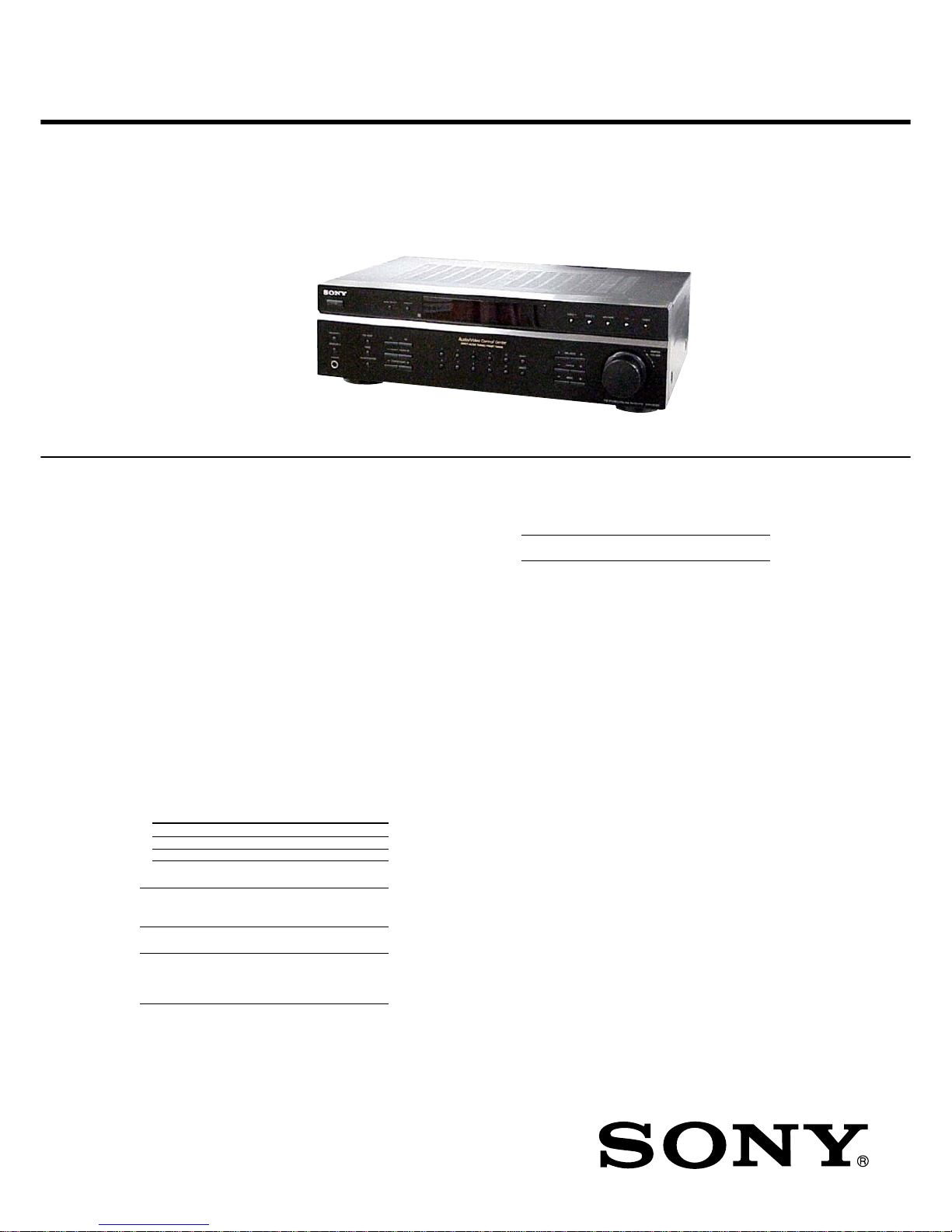
Sony STR DE197 - AV Receiver, STR-DE197 Service Manual
1
SERVICE MANUAL
US Model
Canadian Model
AEP Model
STR-DE197
FM STEREO/FM-AM RECEIVER
AUDIO POWER SPECIFICATIONS
POWER OUTPUT AND TOT AL
HARMONIC DISTORTION:
(Models of area code US only)
With 8 ohm loads, both channels driven, from
20 – 20,000 Hz; rated 100 watts per channel
minimum RMS power, with no more than
0.09 % total harmonic distortion from 250
milliwatts to rated output.
Amplifier section
POWER OUTPUT
Models of area code US, CND
Power Output a t Ster eo Mode
(8 ohms 1 kHz, THD 0.7 %)
125 W + 125 W
1)
Models of ar ea code AEP
Power Output a t Ster eo Mode
(8 ohms 1 kHz, THD 0.7 %)
100 W + 100 W
1)
1) Measur ed under the f ollowing conditions:
Area code Power requir ements
US, CND 120 V A C, 60 Hz
AEP 230 V AC, 50 Hz
Frequenc y response
CD, MD/TAPE, 20 Hz – 50 kHz
VIDEO 1, 2 +0/–0.5 dB (with bass
boost and tone bypassed)
Inputs (Analog)
CD, MD/TAPE, Sensiti vity: 500 mV
VIDEO 1, 2 Impedance: 50 kilohms
S/N
2)
: 85 dB
(A, 500 mV
3)
)
2) INPUT SHOR T (with bass boost and tone b ypassed).
3) W eighted netw ork, input le vel.
SPECIFICATIONS
Outputs (Analog)
MD/TAPE (OUT), V oltage: 500 mV
VIDEO 1 (AUDIO OUT) Impedance: 10 kilohms
Bass Boost: +8 dB at 70 Hz
Tone: ±10 dB at 100 Hz and
10 kHz
FM tuner section
Tuning r ang e 87.5 – 108.0 MHz
Antenna FM wire antenna
Antenna terminals 75 ohms, unbalanced
Inter media te frequenc y 10.7 MHz
Sensiti vity
Mono: 18.3 dBf, 2.2 µV/75 ohms
Stereo: 38.3 dBf, 22.5 µV/75 ohms
Usable sensiti vity 11.2 dBf, 1 µV/75 ohms
S/N
Mono: 76 dB
Stereo: 70 dB
Harmonic distortion at 1 kHz
Mono: 0.3%
Stereo: 0.5%
Separation 45 dB at 1 kHz
Frequenc y response 30 Hz – 15 kHz,
+0.5/–2 dB
Selecti vity 60 dB at 400 kHz
Ver. 1.5 2007. 05
9-877-864-06
2007E04-1
© 2007. 05
Sony Corporation
Home Audio Division
Published by Sony Techno Create Corporation
– Continued on next page –
Photo: Black type
2
STR-DE197
AM tuner section
Tuning range
Models of area code US, CND
With 10-kHz tuning scale: 530 – 1,710 kHz
4)
With 9-kHz tuning scale: 531 – 1,710 kHz
4)
Models of area code AEP
With 9-kHz tuning scale: 531 – 1,602 kHz
Antenna Loop antenna
Intermediate frequency 450 kHz
Usable sensitivity 50 dB/m (at 1,000 kHz or
999 kHz)
S/N 54 dB (at 50 mV/m)
Harmonic distortion 0.5 % (50 mV/m,
400 Hz)
Selectivity
At 9 kHz: 35 dB
At 10 kHz: 40 dB
4) You can change the AM tuning scale to 9 kHz or
10 kHz. After tuning in any AM station, turn off
the receiver. Hold down PRESET TUNING + and
press ?/1. All preset stations will be erased when
you change the tuning scale. To reset the scale to
10 kHz (or 9 kHz), repeat the procedure.
General
Power requirements
Area code Power consumption
US, CND 120 V AC, 60 Hz
AEP 230 V AC, 50/60 Hz
Power consumption
Area code Power consumption
US 190 W
CND 270 VA
AEP 210 W
Power consumption (during standby mode)
0.5 W
AC outlets
Area code AC outlets
US, CND 1 switched, 120 W/1A MAX
AEP 1 switched, 100 W MAX
Dimensions 430 × 132.5 × 302 mm
(17 × 5 1/4 × 11 7/8 inches)
including projecting parts
and controls
Mass (Approx.) 7.0 kg (15 lb 7 oz)
Supplied accessories
FM wire antenna (1)
AM loop antenna (1)
Remote commander RM-U185 (1)
R6 (size-AA) batteries (2)
Design and specifications are subject to change without
notice.
•Abbreviation
CND: Canadian model
1.5 k
Ω
0.15 µF
AC
voltmeter
(0.75 V)
To Exposed Metal
Parts on Set
Earth Ground
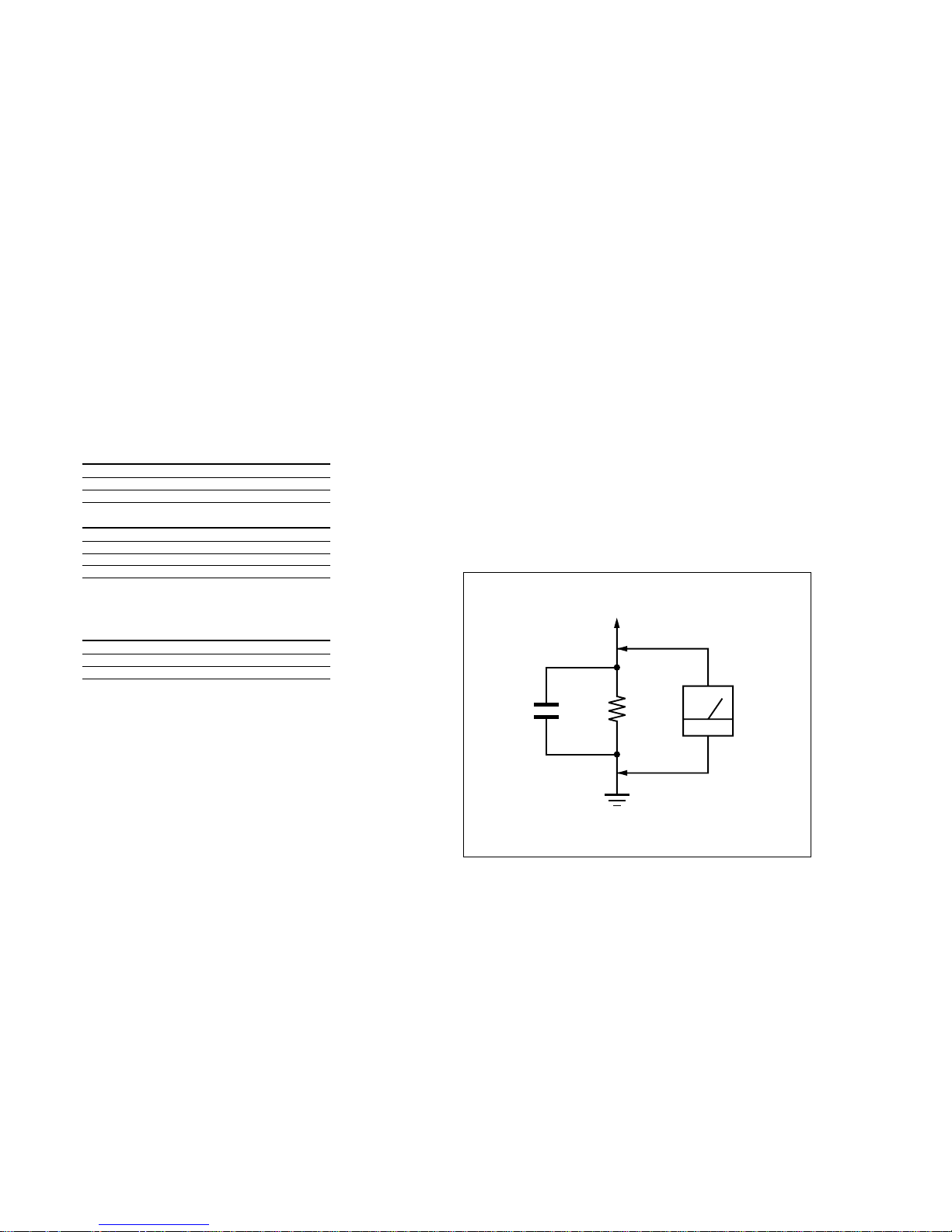
Fig. A. Using an AC voltmeter to check AC leakage.
SAFETY CHECK-OUT
After correcting the original service problem, perform the following
safety check before releasing the set to the customer:
Check the antenna terminals, metal trim, “metallized” knobs, screws,
and all other exposed metal parts for A C leakag e. Check leakage as
described below.
LEAKAGE TEST
The AC leakage from any exposed metal part to earth ground and
from all exposed metal parts to any exposed metal part having a
return to chassis, must not exceed 0.5 mA (500 microamperes).
Leakage current can be measured by any one of three methods.
1. A commercial leakage tester, such as the Simpson 229 or RCA
WT-540A. Follow the manufacturers’ instructions to use these
instruments.
2. A battery-operated AC milliammeter. The Data Precision 245
digital multimeter is suitable for this job.
3. Measuring the voltage drop across a resistor by means of a V OM
or battery-operated A C v oltmeter. The “limit” indication is 0.75
V, so analog meters must have an accurate low-voltage scale. The
Simpson 250 and Sanwa SH-63Trd are examples of a passive
VOM that is suitable. Nearly all battery operated digital
multimeters that have a 2V AC range are suitable. (See Fig. A)
SAFETY-RELATED COMPONENT WARNING!!
COMPONENTS IDENTIFIED BY MARK 0 OR DOTTED LINE
WITH MARK 0 ON THE SCHEMATIC DIAGRAMS AND IN
THE PARTS LIST ARE CRITICAL TO SAFE OPERATION.
REPLACE THESE COMPONENTS WITH SONY P ARTS WHOSE
PART NUMBERS APPEAR AS SHOWN IN THIS MANUAL OR
IN SUPPLEMENTS PUBLISHED BY SONY.
ATTENTION AU COMPOSANT AYANT RAPPORT
À LA SÉCURITÉ!!
LES COMPOSANTS IDENTIFIÉS PAR UNE MARQUE 0 SUR LES
DIAGRAMMES SCHÉMATIQUES ET LA LISTE DES PIÈCES
SONT CRITIQUES POUR LA SÉCURITÉ DE FONCTIONNEMENT .
NE REMPLACER CES COMPOSANTS QUE PAR DES PIÈCES
SONY DONT LES NUMÉROS SONT DONNÉS DANS CE MANUEL
OU DANS LES SUPPLÉMENTS PUBLIÉS PAR SONY.
3
TABLE OF CONTENTS
1. GENERAL
Main unit ................................................................................. 4
Remote button description....................................................... 6
2. DISASSEMBL Y
2-1. Case ..................................................................................... 7
2-2. Front Panel Section ............................................................. 8
2-3. Back Panel........................................................................... 8
2-4. Main Board ......................................................................... 9
3. TEST MODE ..................................................................... 10
4. DIAGRAMS
4-1. IC Pin Description............................................................. 11
4-2. Circuit Boards Location .................................................... 13
4-3. Block Diagram – Main Section –......................................15
4-4. Block Diagram – Power Section – .................................... 16
4-5. Printed Wiring Boards – Main Section – .......................... 17
4-6. Schematic Diagram – Main Section (1/2) – ...................... 18
4-7. Schematic Diagram – Main Section (2/2) – ...................... 19
4-8. Printed Wiring Boards – Panel Section – .......................... 20
4-9. Schematic Diagram – Panel Section – .............................. 21
4-10. IC Block Diagrams............................................................ 22
5. EXPLODED VIEWS
5-1. Case Section ...................................................................... 23
5-2. Front Panel Section ........................................................... 24
5-3. Chassis Section ................................................................. 25
6. ELECTRICAL PARTS LIST ........................................ 26
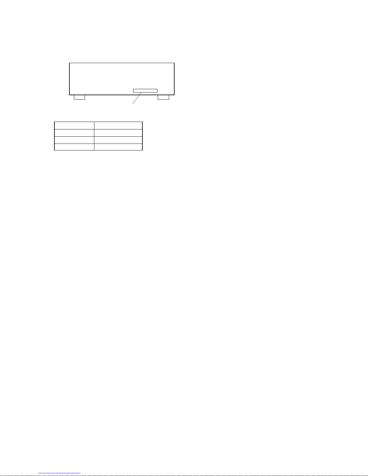
STR-DE197
MODEL IDENTIFICATION
— BACK PANEL —
Part No.
MODEL PART No.
US 4-253-299-0s
AEP 4-253-299-1s
CND 4-253-299-3s
•Abbreviation
CND: Canadian model
4
STR-DE197
SECTION 1
GENERAL
This section is extracted
from instruction manual.
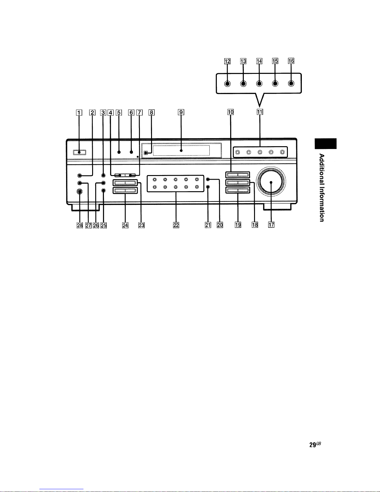
5
STR-DE197
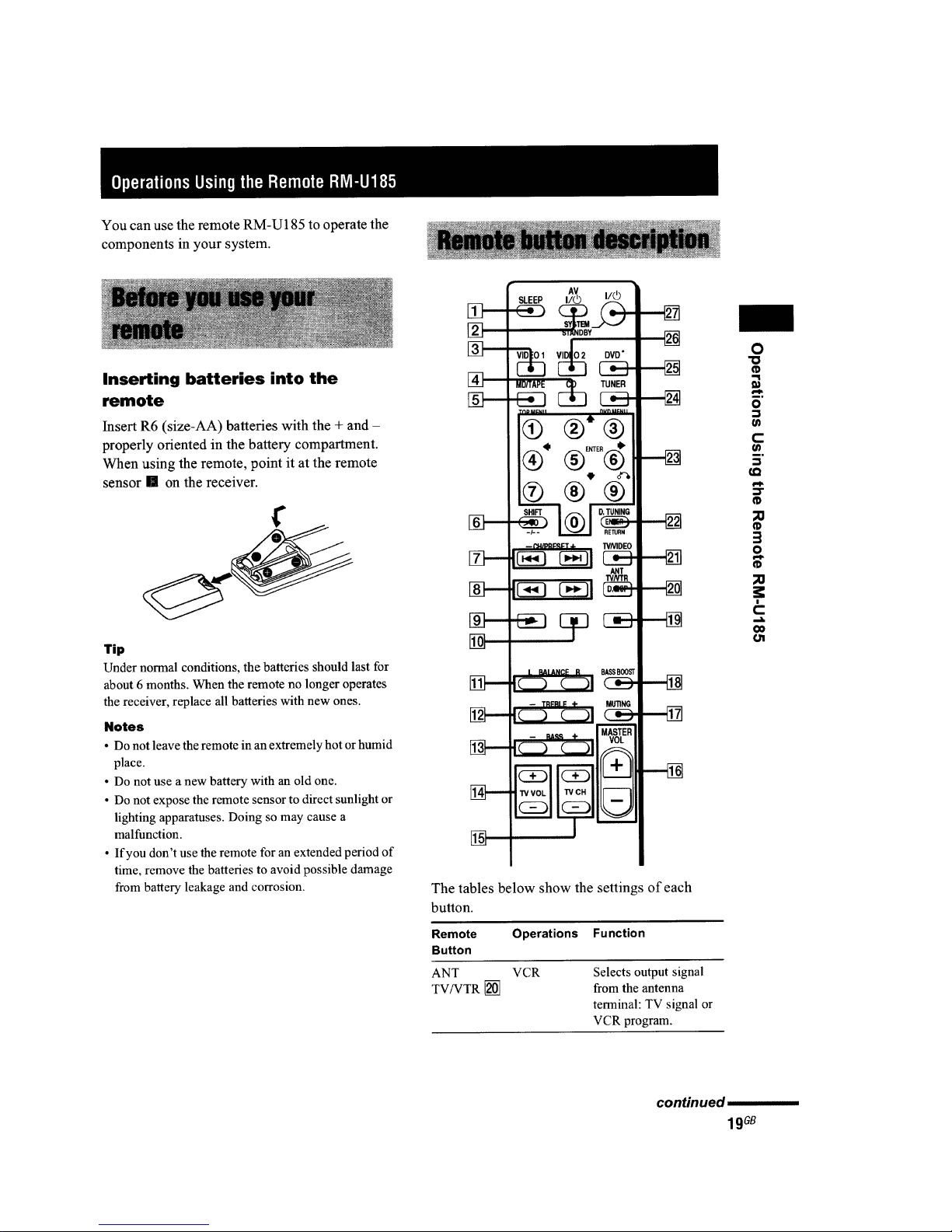
6
STR-DE197
7
STR-DE197
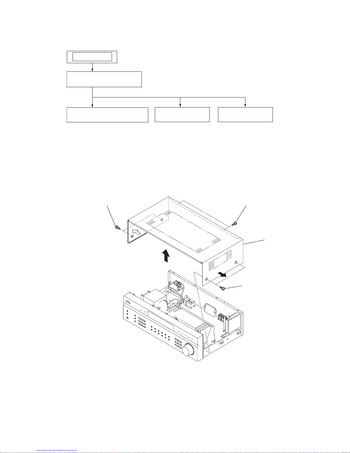
Note : This set can be disassemble according to the following sequence.
SECTION 2
DISASSEMBLY
2-1. CASE
2-1. CASE
(Page 7)
2-2. FRONT PANEL SECTION
(Page 8)
2-3. BACK PANEL
(Page 8)
SET
2-4. MAIN BOARD
(Page 9)
Note : Follow the disassembly procedure in the numerical order given.
1
two screws
(case 3 TP2)
2
two screws
(case 3 TP2)
3
two screws
(case 3 TP2)
4
cas
e
8
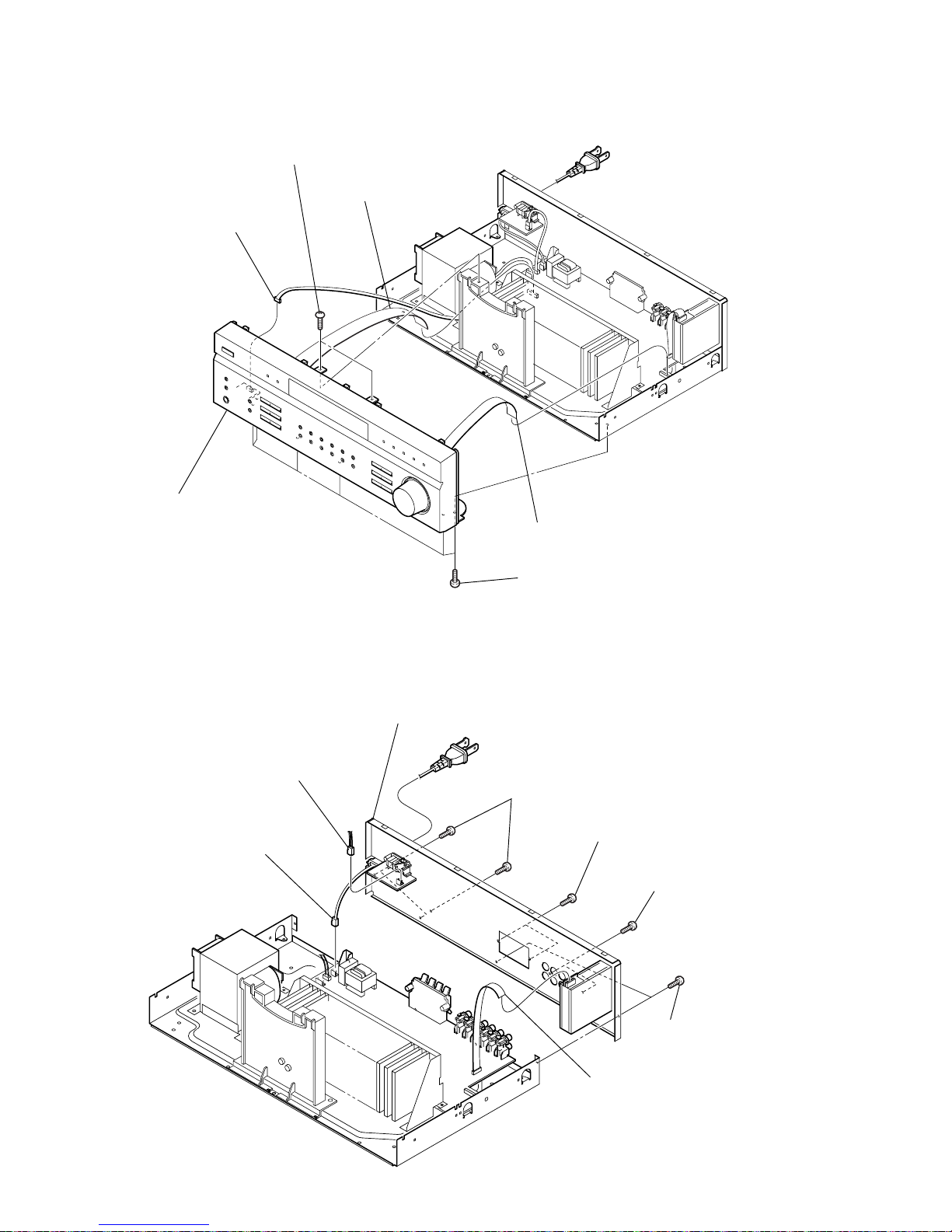
STR-DE197
2-2. FRONT P ANEL SECTION
2-3. BACK P ANEL
6
front panel section
4
two screws
(BVTP3 x 8)
1
CNS2
2
CNS3
3
CNP801
5
six screws
(BVTP3 x 8)
1
connector
2
CNP905
3
CNP901
4
three screws
(BVTP3 x 8)
6
two screws
(BVTP3 x 8)
7
two screws
(BVTP3 x 8)
5
two screws
(BVTP3 x 8)
8
back panel (DE10)
9
STR-DE197
2-4. MAIN BOARD
5
two screws
(+BV SUMITITE (B3))
6
screw
(+BV SUMITITE (B3))
8
MAIN boar
d
7
screw
(+BV SUMITITE (B3))
4
two screws
(+BV SUMITITE (B3))
1
CNP902
3
CNP904
2
CNP903
10
STR-DE197
SECTION 3
TEST MODE
Fluorescent Indicator Tube Test Mode
All fluorescent segments are tested. When this test is activated, all
segments turn on at the same time, then each segment turns on one
after another.
Procedure:
1. While depressing the [VIDEO 1], [VIDEO 2], [MD/TAPE], [CD] and
the [TUNER] buttons simultaneously, press the ?/1 button to
turn on the main power.
2. The FL tube will illuminate in half light on. The following display will be repeated whenever the five function buttons are
pressed.
• Operation of function buttons
3. Press any button other than the function buttons to release the
check mode.
AUTO-BETICAL Check Mode (AEP model)
To auto-scanning and memories of RDS station.
Procedure:
1. While depressing the [MEMORY/ENTER] button, press the
?/1
button to turn on the main power.
2. The message “AUTO-BETICAL SELECT” are scrolled for a
moment and the receiver starts scanning.
AM T uning Interval Selection Mode (US, Canadian model)
Either 9 kHz step or 10 kHz step can be selected for the AM tuning
interval.
Procedure:
1. While depressing the [PRESET TUNING +] button or the [TUN-
ING/CHAR +] button, press the ?/1 button to turn on the main
power.
2. Either the message “9k STEP” or “10k STEP” appears for a
moment and select the desired step.
Software Version Display Mode
The software version is displayed.
Procedure:
1. While depressing the [SPEAKER B] and the [VIDEO 1] buttons
simultaneously, press the ?/1 button to turn on the main power .
2. The destination and the software version are displayed for a
moment.
all light on half light on 1 half light on 2 all light of
f
ex.) US, Canadian model : U
*.**
AEP model : CE *.
**
Area
Software version

11
STR-DE197
SECTION 4
DIAGRAMS
1 to 7 DIG7 to DIG1 O Digit drive signal output to the vacuum fluorescent display (FL201).
8 +5V — Power supply pin (+5 V)
9CLOSerial clock signal output to FM/AM tuner pack.
10 DO O Serial data signal output to FM/AM tuner pack.
11 DI I Serial data signal input from FM/AM tuner pack.
12 CE O Serial chip enable signal output to FM/AM tuner pack.
13 VOL DATA O Serial data signal output to sound control IC.
14 VOL CL O Serial clock signal output to sound control IC.
15 RDS DATA I RDS data signal input from FM/AM tuner pack. (AEP model only)
16 PROTECTOR I Overload detection signal input
17 RESET I Reset signal input
18 TUNED I TUNED indicator detection signal input from FM/AM tuner pack.
19 STEREO I STEREO indicator detection signal input from FM/AM tuner pack.
20 AVSS — Analog ground
21 VERSION I Destination select signal input (Fixed at H: US, Canadian model, L: AEP model)
22 FM SIGNAL OUT I
FM/AM signal meter voltage detection signal input from FM/AM tuner pack.
(AEP model only)
23 to 28 AD6 to AD1 I Function keys signal input
29 AVDD — A/D converter power supply pin (+5 V)
30 AV.REF — A/D converter reference voltage input (+5 V)
31 — — Not used. (Connect to AV.REF pin in this set)
32 OPEN — Not used. (Open)
33 GND — Ground
34 X1 I Master clock input (4.19 MHz)
35 X2 O Master clock output (4.19 MHz)
36 REC SW1 O VIDEO 1 ON/OFF signal output
37 REC SW2 O MD/TAPE ON/OFF signal output
38, 39 VOL A, VOL B I Master volume JOG data input A, B
40 FUNC.MUTE O Not used. (Fixed at L in this set)
41 CK O Serial clock signal output to electronic volume IC.
42 DATA O Serial data signal output to electronic volume IC.
43 STB O Serial data strobe signal output to electronic volume IC.
44 SYS.POWER I System power signal input
45 AC MUTE O A-Class mute signal output
46 RDS INT I RDS clock signal input from FM/AM tuner pack. (AEP model only)
47 STOP I Stop signal input from reset/+5.6V regulator IC.
48 VSS — Ground
49 SIRCS I Sircs signal input from remote control receiver IC.
50 TUNER MUTE O Muting control signal output to FM/AM tuner pack.
51 — — Not used. (Open)
52 +5V — Power supply pin (+5 V)
53 BASS B. LED O BASS BOOST LED drive signal output
54 SPK A LED O SPEAKER A LED drive signal output
55 SPK B LED O SPEAKER B LED drive signal output
4-1. IC PIN DESCRIPTION
• IC201 µPD78045FGF-134-3B9 (SYSTEM CONTROLLER, FL DISPLAY DRIVER)
Pin No. Pin Name I/O Pin Description
12
STR-DE197
56 RY R1 COIL O Power relay (12V) drive signal output
57 RY POWER O AC power relay (9V) drive signal output
58 RY A O Speaker A relay (12V) drive signal output
59 RY B O Speaker B relay (12V) drive signal output
60 RY HP O Phones relay (12V) drive signal output
61 — — Not used. (Open)
62 to 70 S15 to S7 O Segment drive signal output to the vacuum fluorescent display (FL201).
71 VLOAD — Power supply pin (–24 V)
72 to 77 S6 to S1 O Segment drive signal output to the vacuum fluorescent display (FL201).
78 to 80 DIG10 to DIG8 O Digit drive signal output to the vacuum fluorescent display (FL201).
Pin No. Pin Name I/O Pin Description

13
STR-DE197
4-2. CIRCUIT BOARDS LOCATION
AC OUTLET board
MAIN board
FUNCTION KEY boar
d
VOLUME board
DISPLAY board
POWER board
H.PHONE board
14
STR-DE197
THIS NOTE IS COMMON FOR PRINTED WIRING
BOARDS AND SCHEMATIC DIAGRAMS.
(In addition to this, the necessary note is
printed in each block.)
for schematic diagram:
• All capacitors are in µF unless otherwise noted. (p: pF)
50 WV or less are not indicated except for electrolytics
and tantalums.
• All resistors are in Ω and 1/
4
W or less unless otherwise
specified.
•
f
: internal component.
• 2 : nonflammable resistor.
• 1 : fusible resistor.
• C : panel designation.
• A : B+ Line.
• B : B– Line.
•Voltage and waveforms are dc with respect to ground
under no-signal (detuned) conditions.
no mark : FM
•Voltages are taken with a VOM (Input impedance 10 MΩ).
Voltage variations may be noted due to normal production tolerances.
•Waveforms are taken with a oscilloscope.
Voltage variations may be noted due to normal production tolerances.
• Circled numbers refer to waveforms.
• Signal path.
F : TUNER (FM/AM)
L : VIDEO (AUDIO)
J : CD (ANALOG)
• Abbreviation
CND : Canadian model.
for printed wiring boards:
• X : parts extracted from the component side.
•
f
: internal component.
• : Pattern from the side which enables seeing.
• Abbreviation
CND : Canadian model.
C
B
These are omitted.
E
Q
B
These are omitted.
C
Q
Q
E
BCE
Note:
The components identified by mark 0 or dotted
line with mark 0 are criti-
cal for safety.
Replace only with part
number specified.
Note:
Les composants identifiés par
une marque 0 sont critiques
pour la sécurité.
Ne les remplacer que par une
piéce portant le numéro
spécifié.
STR-DE197
15 15
STR-DE197
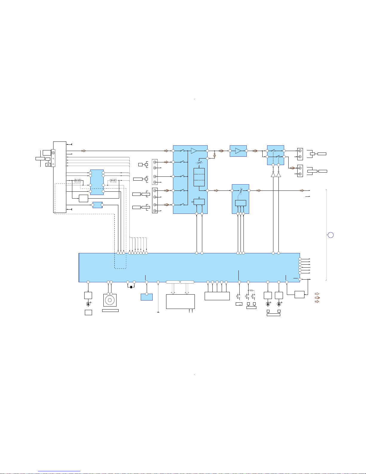
4-3. BLOCK DIAGRAM — MAIN SECTION —
9
7
5
3
1
1422
49 71 2877 - 72,70 - 62 7 - 1,80 - 78 27 26 25 24 44 23 54 1734
35
15 46 19 18 50 12 10 11 9 13 37 36
60
58
59
16
56
57
47
13 5
41 42 43
32 3 1 1 2
4 3
3
10 8
12 11
5 6
2 3
7
LED
DRIVER
Q204
LED
DRIVER
Q206
55
LED
DRIVER
Q205
KEY MATRIX
FL201
VACUUM
FLUORESCENT
DISPLAY
1
REMOTE
CONTROL
RECEIVER
IC202
29
20 3 2
8 9 1015 14
3853 39
1 3
TREBLE
L
MIDDLE
L
BASS
L
CONTROL
VOLUME
CONTROL
STEREO
TUNED
MUTE
CE
DI
DO
CL
FM SIGNAL OUT
RDS DATA
RDS INT
STEREO
TUNED
TUNER MUTE
CE
DO
DI
CL
VOL CL
VOL DATA
CK
DATA
STB
REC SW2
REC SW1
RY HP
RY A
RY B
PROTECTOR
RY R1 COIL
RY POWER
STOP
ST-R
R-CH
R-CH
R-CH
R-CH
R-CH
R-CH
R-CH
ST-L
HP RELAY
SPK A RELAY
RESET
SPK B RELAY
PROTECTOR SIG
R1 COIL RELAY
POWER RELAY
STOP SIGNAL
RESET
SWITCH
Q201,202
BASS B.LED
VOL A
VOL B
X1
X2
VLOAD
AD1
AD2
AD3
AD4
AD5
SYS.POWER
AD6
SPK A LED
SPK B LED
DIG1
I
DIG10
S1
I
S15
SIRCS
S201 S202 S203
I
/
I
SPEAKER
D205 D206
SPEAKER
AB
X201
4.19MHz
D203
RV201
MASTER VOLUME
BASS
BOOST
AB
S204-213,
215-236,
238,239
SYSTEM CONTROLLER,
FL DRIVER
IC201
J801 (1/2)
J802 (1/2)
-1
L
-2
R
INCD
IC906
LEVEL
SHIFT
IC905
US,CND MODEL
-5
L
-6
R
INMD/TAPE
J801 (2/2)
VIDEO 1,MD/TAPE
SELECT
IC404
AUDIO AMP
IC403
SOUND CONTROL
IC401
-3
L
-4
R
OUT
MD/TAPE
J802 (2/2)
-3
L
-4
R
AUDIO OUT
VIDEO 1
-1
L
-2
R
AUDIO INVIDEO 2
-5
L
-6
R
AUDIO INVIDEO 1
FM 75Ω
COAXIAL
AM
ANTENNA
10V
L CH
R CH
MUTE
CE
CLOCK
DO
TUNED
STEREO
STEREO
TUNED
MUTE
CE
CL
DO
FM SIGNAL
RDS DATA
RDS INT
VDD3.3V
R-CH
+10V
3.3V
LEVEL
SHIFT
-24V F1 F2
REC L
VOL L
OUT L
TUNER
L
CD L
MD L
VIDEO 2
LINL
OUT
VIDEO 1
CLK
DATA
CLK
STB
DATA
ELECTRONIC
VOLUME
IC402
Q424
INV.
Q474
INV.
TN1
FM/AM TUNER PACK
DATA
DI
AEP MODEL
POWER
SECTION
A
LEVEL
SHIFT
Q905,906
US,CND MODEL
• Signal path
: TUNER (FM/AM)
: VIDEO (AUDIO)
: CD (ANALOG)
• R-ch is omitted due to
same as L-ch.
• Abbreviation
CND : Canadian model
(Page 16)
STR-DE197
1616
STR-DE197
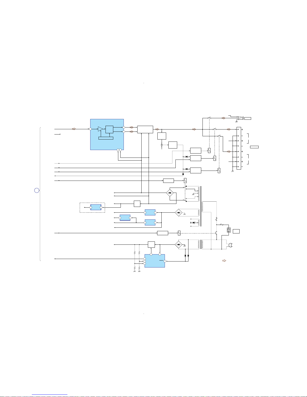
4-4. BLOCK DIAGRAM — POWER SECTION —
6
2
3
DRIVE
POWER AMP
Q701-704
BIAS
14 15
-24V
REG
Q904
+5V REG
IC902
3 1
+10V REG
IC903
3 1
67
8
2
53
RELAY DRIVER
Q783
RELAY DRIVER
Q903
-5V REG
IC907
3 2
+3.3V REG
IC904
3 1
RELAY DRIVER
Q901
+5.6V
REG
Q902
RELAY DRIVER
Q782
RELAY DRIVER
Q781
+B
-B
-24V
+5V
+3.3V
-5V
AEP MODEL
+10V
RY+B
+5.6V
OUT C V+
RESET
VSA
VSC
RESET/+5.6V REG
IC901
VSB/SESIN
F1
-24V
F2
RY982
F902
F901
D913
RY981
RY781
R-CH
RY782
RY783
RECT
D901-904
RECT
D908-911
RECT
D907
T901
POWER
TRANSFORMER
T902
POWER
TRANSFORMER
D905 D906
CNJ901
AC
OUTLET
SWITCHED 120W/1A MAX
AC 120V 60 Hz (US,CND)
SWITCHED 100W MAX
(AEP)
~
AC IN
-B
+B
VCC
VEE
PRE DRIVER
IC601
PRE
DRIVE
IN 1
+VOUT
-VOUT
CURRENT
DET
Q705,706
PROTECT
SWITCH
Q784-786
R-CH
J803
PHONES
TM801
SPEAKERS
IMPEDANCE
USE 8-16Ω
L
R
A
L
R
B
R-CH
R-CH
ST-L
ST-R
HP RELAY
SPK A RELAY
SPK B RELAY
PROTECTOR SIG
R1 COIL RELAY
POWER RELAY
STOP SIGNAL
R-CH
MAIN
SECTION
A
D786
D787
D789
• Signal path
: TUNER (FM/AM)
• R-ch is omitted due to
same as L-ch.
• Abbreviation
CND : Canadian model.
(Page 15)
STR-DE197
17 17
STR-DE197
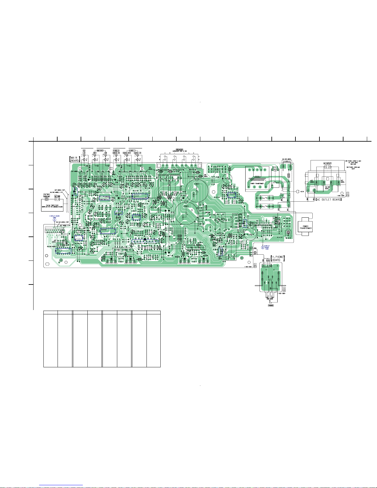
4-5. PRINTED WIRING BOARDS — MAIN SECTION — • Refer to page 13 for Circuit Boards Location and page 14 for Common Note on Printed Wiring Boards.
1
A
B
C
D
E
F
G
234567891011 12 13 14
CNP905
T901
CNJ901
J803
CNP801
IC401
JW485
JW491
JW477
JW415
JW469
JW430
JW470
JW488
JW493
JW489
JW501
JW495
JW498
JW487
JW506
JW428
JW480
JW416
JW504
JW417
JW405
JW473
JW515
TP1
JW410
JW520
JW479
JW490
JW494
JW420
JW448
JW438
JW406
JW503
JW419
JW414
JW418
JW901
JW451
JW457
JW517
JW424
JW518
JW484
JW456
JW507
JW496
JW467
JW455
JW431
JW514
JW513
JW499
JW445
JW478
JWH2
JWH3
JWH5
JW400
JW404
JW411
JW412
JW413
JW421
JW423
JW425
JW427
JW432
JW433
JW434
JW435
JW437
JW439
JW440
JW441
JW442
JW443
JW449
JW452
JW453
JW454
JW458
JW461
JW482
JW483
JW471
JW497
JW500
JWH4
JW450
JW505
JW444
JW481
JW508
JW464
JW426
JW446
JW468
JW486
JW476
JW447
JW502
JW900
JW436
JW492
JW510
JW511
JW459
JW460
JW474
JW475
TP4
JW472
JW465
JW466
JWH1
JW462
JW509
JW512
JW402
JW401
JW403
D915
CC403
R943
Q906
CC455
CC405
CC407
CC457
CC411
CC459
CC409
CC461
CC752
CC702
Q905
R946
C940
RR702
R945
R947
IC905
R942
CC453
CC701
RR752
RR751
RR701
C941
CC401
CC451
CC751
R944
IC907
R697
Q754Q753
R755
Q706
R762
IC902
R428
C413
C419
Q701
R602
R702
R654
R763
R713
J801
R453
R456
Q786
C905
C912
C464
R471
Q752
D907
C929
IC402
J802
R454
IC901
C915
Q704
C914
R403
R902
RY981
TM801
C414
D784
T902
D751
R416
F901
C906
RY982
CNP902
R903
R905
C903
D905
Q703
Q702
R711
C424
R790
R709
C653
C604
C603
R753
R918
B901
R455
R467
R458
C910
R482
C704
R407
C930
C924
C465
R701
CNP901
R707
R907
R910
R408
R459
R460
R409
R410
R461
R412
R462
C454
C404
C456
C406
C458
C408
C460
C410
C462
C412
R423
C425
Q474
Q424
C472
C422
C467
R920
R421
C420
C470
R466
R415
R919
R465
C466
C702
R474
R472
C471
R604
C605
C658
C421
R418
C928
R484
R427
R791
R789
R764
D788
R714
D783
Q782
Q783
R783
D701
C654
R710
R784
CNS1
R761
R923
C913
CNP904
CN801
D781
C782
D981
Q901
D787
Q903
Q781
CNS3
C791
EP901
R904
C923
C922
D785
D909
D910
D911
D908
C781
R457
R424
D786
D789
R917
C917
C920
C919
C921
D912
D913
R405
R452
R402
C927
R425
C474
R478
R473
C475
D782
R406
R475
R404
R477
C926
TN1
C476
C607
C908
C701
C751
R792
R793
C463
CNS2
R603
R463
C652
R652
L751
R422
R653
C657
R930
R655
R656
D914
R414
R788
R605
R606
Q784
C402
R901
IC404
R782
R417
C602
R468
Q756
C916
R915
CNP903
Q902
C490
R708
C918
Q705
R929
C902
R914
R916
RY783
R786
C468
R411
R908
R712
D906
R787
C904
Q904
C415
IC904
C931
Q751
R754
L701
R483
R705
R760
R413
C484
C485
R913
R781
C754
IC403
R906
R926
C426
R476
R426
C608
CN905
C469
R758
IC906
R757
C418
R785
R451
C755
C655
R401
RY782
D901
C909
C703
R909
C705
R912
C483
C901
C753
C925
D902
R751
R752
R464
RY781
R706
Q755
Q785
C417
C416
R911
F902
R756
C752
D903
D904
R703
D982
R481
R485
C907
C911
C452
R759
R795
R794
C942
IC601
IC903
R704
JW422
C651
C601
C606
C656
JW516
JW429
JW407
R941
(Page 20)
(Page 20)
D701 D-6
D751 D-6
D781 E-9
D782 C-6
D783 C-6
D784 D-6
D785 D-6
D786 E-9
D787 E-9
D788 D-6
D789 D-10
D901 B-8
D902 B-9
D903 D-9
D904 B-8
D905 B-8
D906 B-8
• Semiconductor Location
Ref. No. Location
D907 D-7
D908 D-11
D909 D-11
D910 D-11
D911 D-11
D912 E-8
D913 D-9
D914 C-4
(D915) D-2
D981 E-9
D982 B-11
IC401 C-3
IC402 D-3
IC403 D-5
IC404 C-5
IC601 E-5
IC901 C-9
IC902 D-9
IC903 C-4
IC904 C-2
(IC905) E-2
IC906 E-2
(IC907) E-8
Q424 C-5
Q474 C-5
Q701 E-4
Q702 F-4
Q703 E-4
Q704 E-4
Q705 E-5
Q706 E-6
Q751 E-7
Q752 E-7
Q753 E-7
Q754 E-8
Q755 E-7
Q756 E-7
Q781 D-9
Q782 E-8
Q783 E-8
Q784 D-6
Q785 D-6
Q786 D-5
Q901 B-8
Q902 B-9
Q903 D-9
Q904 E-8
(Q905) E-2
(Q906) D-2
Ref. No. Location Ref. No. Location Ref. No. Location
( ) : AEP model only
STR-DE197
1818
STR-DE197
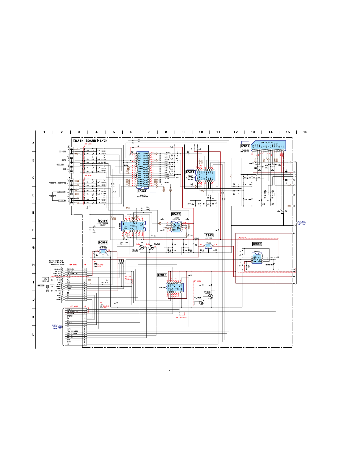
4-6. SCHEMATIC DIAGRAM — MAIN SECTION (1/2) — • Refer to page 14 for Common Note on Schematic Diagram and page 22 for IC Block Diagrams.
IC B/D
IC B/D
IC B/D
LEVEL SHIFT
LEVEL SHIFT
R415
R416
R465
R466
R474
R481
R482
R483
R484
R697
IC906
D914
C406
C408
C412
C421
C426
C456
C458
C462
C469
C471
C476
C484
C485
C606 C656
C924
C926
C942
C414
C415
C464
C465
C416
C417
C466
C467
C418
C468
C927
R602 R652
C410
C460
C413
C420
C463
C470
C425
C490
R926
R403 R404
R409 R410
R453 R454
R459 R460
R464
R401 R402
R405 R406
R407 R408
R411 R412
R451 R452
R455 R456
R457 R458
R461 R462
R475
R417
R418
R423
R467
R468
R472
R473
R421
R422
R477
C474C424
R424
IC601
R414
J801
J802
IC403
IC402
C601 C651
C929
R656R606
C402
C452
C454
C404
C483
R426
R476
R425
R428
R427
R478
R918
R919
R920
C419
R463
R413
R471
C475
C928
C925
C422 C472
R485
C657
C607
R655
R605
R604
R603 R653
R654
R929
R930
C930
IC404
CC451
CC401
CC453
CC403
CC455
CC405
CC457
CC407
CC459
CC409
CC461
CC411
IC401
C658
C608
C603 C653
C654
C604
C652
C602
C605 C655
IC904
IC903
Q474
Q424
IC905R942
R943
R945
C940R944
R941 C941
D915
JW900
C931
R947R946
Q906
Q905
JW901
TN1
CNS1
CNS2
(Page 21)
(Page 19)
STR-DE197
19 19
STR-DE197
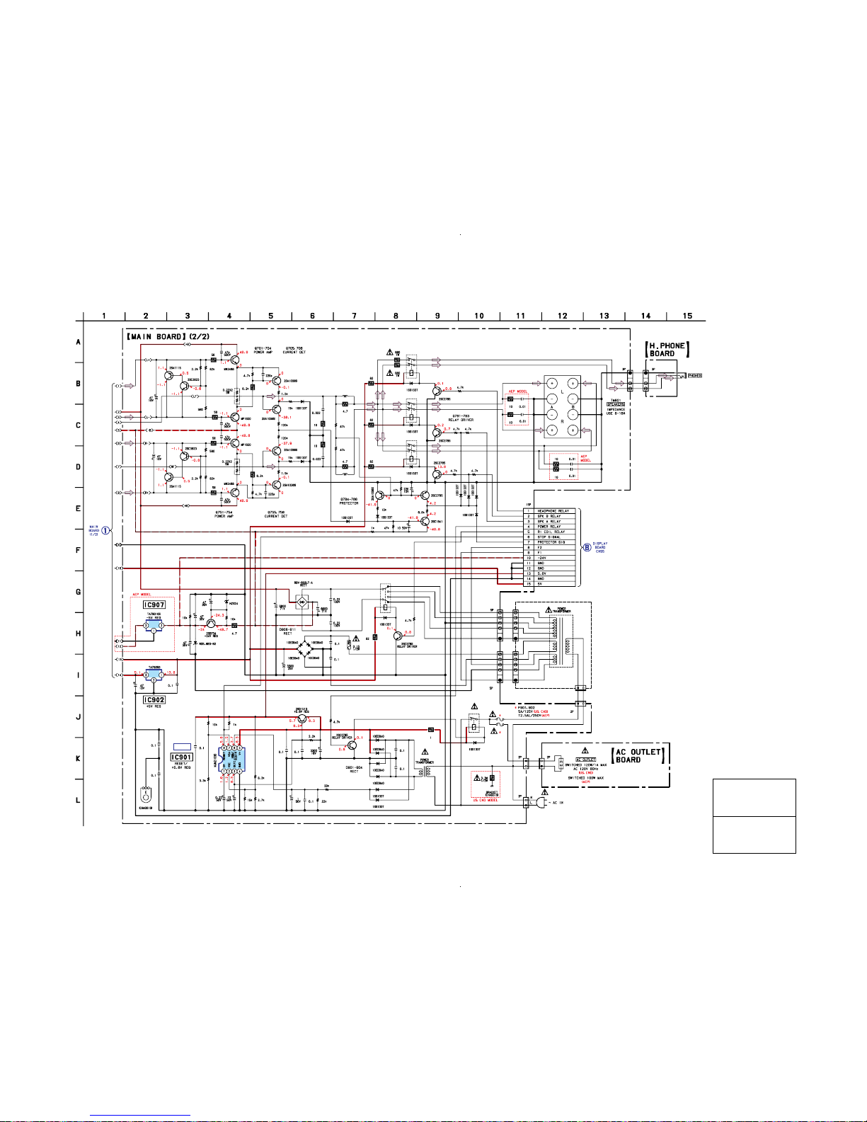
4-7. SCHEMATIC DIAGRAM — MAIN SECTION (2/2) — • Refer to page 14 for Common Note on Schematic Diagram and page 22 for IC Block Diagrams.
IC B/D
Q703
Q704
Q753
Q754
C704
C754
D905
D906
D981
D982
F901
F902
Q701
Q702
Q751
Q752
Q781
Q782
Q783
Q785
Q786
R703
R707
R708
R709
R711
R714
R753
R757
R758
R759
R761
R763
R764
R781
R782
R783
R786
R787
R788
R794
R901
R904
R905
R906
R910
R911
R912
R916
D912
R704
R705
R754
R755
D901
D902
D903
D904
D908
D910
D909
D911
C782
C791
C901
C902
C903
C906
C908
C910
C911
C912
C913
C916
C917
C919
C920
C921
C922
CNP902
CNP904
R710
R760
R791
C905
R917
R923
R789
CNP903
C914
CNS3
D701
D781
D782
D783
D784 D785
D786
D787
D788
C701
R701 R702
C751
R752R751
D751
C705
C755
R762
R712
R713
L751
L701
C923
C909
R909 R908
R907
C907
C904
CNP901
CN905
R902
R784
R785
R795
R793
C781
R790
C915
C918
R913
R914
D789
CN801
RY781
RY782
RY783
R706
RY981
C702
C703
Q705
Q706
Q756
C753
R756
C752
Q755
Q784
RR701 CC701
RR751
CC751
RR702 CC702
RR752
CC752
J803
CNP801
IC907
IC902
Q904
D913
D907
Q903
EP901
IC901
Q902
Q901
RY982
R903
B901
CNJ901
T901
T902
CNP905
R792
R915
TM801
(Page
18)
(Page 21)
The components identified by
mark 0 or dotted line with mark
0 are critical for safety.
Replace only with part number
specified.
Les composants identifiés par
une marque 0 sont critiques
pour la sécurité.
Ne les remplacer que par une
pièce portant le numéro spécifié.
 Loading...