

Page 1
STR-DE1015G
SERVICE MANUAL
US Model
Canadian Model
SPECIFICATIONS
— Continued on next page —
MICROFILM
FM STEREO FM-AM RECEIVER
— 1 —
Page 2
— 2 —
Page 3
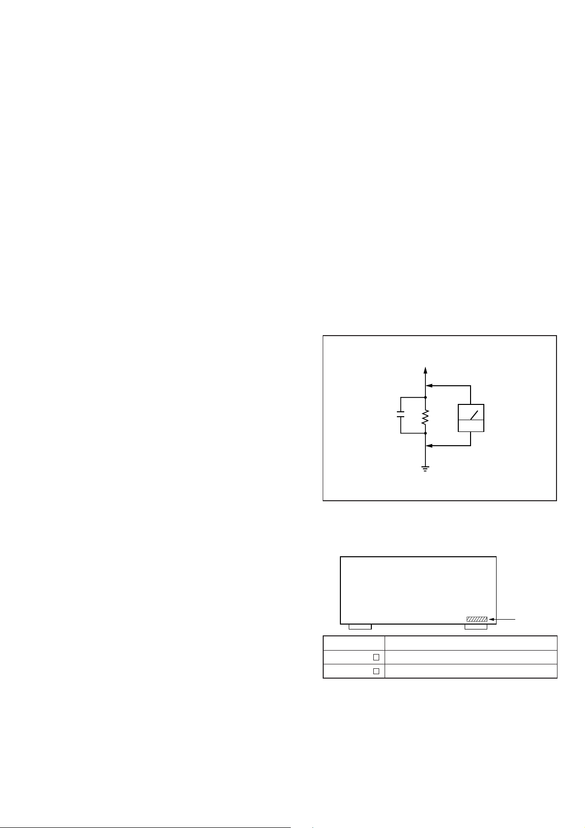
TABLE OF CONTENTS
SAFETY CHECK-OUT
1. SERVICING NOTE
.......................................................... 4
2. GENERAL .......................................................................... 5
3. DISASSEMBLY
3-1. Front Panel .......................................................................... 26
3-2. Balance Board, Display Board and Volume Board............. 26
4. TEST MODE ..................................................................... 27
5. ELECTRICAL ADJUSTMENTS ............................... 28
6. DIAGRAMS
6-1. IC Pin Functions................................................................. 30
6-2. Circuit Boards Location ...................................................... 47
6-3. Block Diagrams
• Input/Output Section........................................................ 49
• Power Amp Section ......................................................... 51
• DA Section....................................................................... 53
• DSP Section ..................................................................... 55
• AC-3 (RF) Section........................................................... 57
• OSD Section .................................................................... 59
• OSD Control Section ....................................................... 61
• Panel Section ................................................................... 63
• Power Section .................................................................. 65
6-4. Printed Wiring Board — Input/Output Section — ............. 68
6-5. Schematic Diagram — Input/Output Section — ................ 71
6-6. Schematic Diagram — Power Amp Section —.................. 75
6-7. Printed Wiring Board — Power Amp Section — ............... 79
6-8. Printed Wiring Board — Digital Section — ....................... 83
6-9. Schematic Diagram — Digital (D/A) Section — ............... 87
6-10. Schematic Diagram — Digital (Control) Section — ....... 91
6-11. Schematic Diagram
— Digital (Dolby AC-3) Section —................................. 95
6-12. Printed Wiring Board — Panel Section —....................... 98
6-13. Schematic Diagram — Panel Section — ....................... 101
6-14. Schematic Diagram — OSD Section — ........................ 105
6-15. Printed Wiring Board — OSD Section —...................... 109
6-16. IC Block Diagrams......................................................... 112
After correcting the original service problem, perform the following safety checks before releasing the set to the customer:
Check the antenna terminals, metal trim, “metallized” knobs, screws,
and all other exposed metal parts for A C leakage. Check leakage as
described below.
LEAKAGE
The AC leakage from any exposed metal part to earth Ground and
from all exposed metal parts to any exposed metal part having a
return to chassis, must not exceed 0.5 mA (500 microampers). Leakage current can be measured by any one of three methods.
1. A commercial leakage tester, such as the Simpson 229 or RCA
WT-540A. Follow the manufacturers’ instructions to use these
instruments.
2. A battery-operated AC milliammeter. The Data Precision 245
digital multimeter is suitable for this job.
3. Measuring the voltage drop across a resistor by means of a VOM
or battery-operated A C v oltmeter. The “limit” indication is 0.75
V, so analog meters must have an accurate low-voltage scale.
The Simpson 250 and Sanwa SH-63Trd are examples of a passive VOM that is suitable. Nearly all battery operated digital
multimeters that have a 2V AC range are suitable. (See Fig. A)
To Exposed Metal
Parts on Set
0.15µF
1.5k
Ω
Earth Ground
AC
voltmeter
(0.75V)
Fig. A. Using an AC voltmeter to check AC leakage.
7. EXPLODED VIEWS
7-1. Case Section...................................................................... 117
7-2. Front panel Section ........................................................... 118
7-3. OSD Board Section........................................................... 119
7-4. Chassis Section ................................................................. 120
8. ELECTRICAL PARTS LIST ...................................... 121
Notes on chip component replacement
• Never reuse a disconnected chip component.
• Notice that the minus side of a tantalum capacitor may be
damaged by heat.
SAFETY-RELATED COMPONENT WARNING !!
COMPONENTS IDENTIFIED BY MARK ! OR DO TTED LINE
WITH MARK ! ON THE SCHEMATIC DIAGRAMS AND IN
THE PARTS LIST ARE CRITICAL TO SAFE OPERATION.
REPLACE THESE COMPONENTS WITH SONY PARTS
WHOSE PART NUMBERS APPEAR AS SHOWN IN THIS
MANUAL OR IN SUPPLEMENTS PUBLISHED BY SONY.
MODEL IDENTIFICATION
— BACK PANEL —
Parts No.
4-989-885-4
4-989-885-5
ATTENTION AU COMPOSANT AYANT RAPPORT
LES COMPOSANTS IDENTIFIÉS P AR UNE MARQUE ! SUR
LES DIAGRAMMES SCHÉMATIQUES ET LA LISTE DES
PIÈCES SONT CRITIQUES POUR LA SÉCURITÉ DE
FONCTIONNEMENT. NE REMPLA CER CES COMPOSANTS
QUE PAR DES PIÈCES SONY DONT LES NUMÉROS
SONT DONNÉS DANS CE MANUEL OU DANS LES
SUPPLÉMENTS PUBLIÉS PAR SONY.
US model
Canadian model
À LA SÉCURITÉ!!
Model
— 3 —
Parts No.
Page 4
SECTION 1
SERVICING NOTE
ALL CLEAR
Mode which erases all the user memories registered in this unit and
sets to setting at shipment.
Procedure:
1. With the power turned OFF, press the POWER button while
pressing the MODE button, AUDIO FUNCTION > and
VIDEO FUNCTION > button simultaneously to turn ON the
power.
2. ALL CLEAR 3/5 will be displayed on the fluorescent indicator
tube, and ALL CLEAR will be executed.
FACTORY SET
Mode which sets the memory of the unit to the setting of adjustment and check at factory. (Not used for servicing.)
Procedure:
1. With the power turned OFF, press the POWER button while
pressing the MODE button and AUDIO FUNCTION > button
simultaneously to turn ON the power.
2. FACTORY SET will be displayed on the fluorescent indicator
tube, and FACTORY SET will be executed.
Note: In case you return the unit to the customer, do not perform
FACTRY SET. If you do it, perform ALL CLEAR.
Fluorescent indicator tube, LED all lit mode
Adjustment of OSD Screen Position
The position of the screen can be adjusted freely to correct the deviation of the OSD screen caused by the monitor type that users are
using.
1. Move the cursor of the remote commander supplied as an accessory, and display the OSD screen.
2. Click the SET UP of the OSD screen.
3. Next click TV SET.
4. Next click GRAPHIC POSITION SET.
5. The screen for adjusting the OSD screen position will be displayed. Adjust the position with the remote commander supplied
as an accessory.
6. Click EXIT to end.
AM Tuning Step 9 kHz/10 kHz Selection
Method:
1. Turn ON the power, set the AUDIO FUNCTION to AM, and
turn OFF the power.
2. While pressing the TUNING + button or PRESET TUNING +
button, press the POWER button.
3. “AM 9K STEP” or “AM 10k STEP” will be displayed on the FL
display tube.
Procedure:
1. With the power turned OFF, press the POWER button while
pressing the MODE button and VIDEO FUNCTION > b utton
simultaneously to turn ON the power.
2. The fluorescent display tubes and LEDs will all light up. Release the buttons in the order of VIDEO FUNCTION > , and
MODE .
3. The Fluorescent indicator tube display changes as follows by
pressing the DPC MODE .
(Pressing the other buttons will exit this mode.)
9
Fluorescent indicator tubes, LEDs are all lit
DIGITAL
12345
AC-3 RF
SOUND FIELD
DISCRETE PRO LOGIC MONO STEREO
• Press DPC MODE button.
9
Partial lighting of fluorescent indicator tube 1, LEDs are OFF *1
• Press DPC MODE button.
9
Partial lighting of fluorescent indicator tube 2, LEDs are OFF *1
MEMORY
• Press DPC MODE button.
9
Fluorescent indicator tube and all LEDs are OFF
• Press DPC MODE button.
9
*1 Those other than the POWER LED go OFF.
4. To exit the mode, press the POWER button to turn OFF the
power.
— 4 —
Page 5
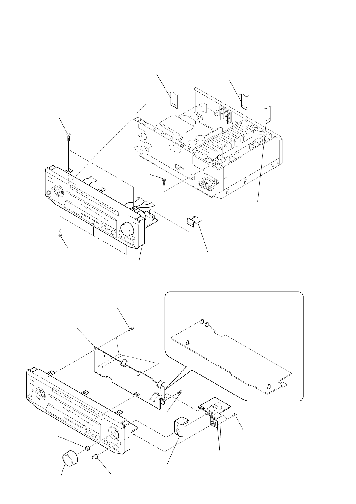
SECTION 3
DISASSEMBLY
Note: Follow the disassembly procedure in the numerical order given.
3-1. FRONT PANEL
3
Flat type wire (19 core)
(CNS701)
1
Three screws
(BVTP3x8)
2
Screw
(BVTP3x8)
4
Flat type wire (CNJ203)
6
Three screws
(BVTP3x8)
7
Front panel
3-2. BALANCE BOARD, DISPLAY BOARD AND VOLUME BOARD
8
0
DISPLAY board
Four screws
(BVTP2.6x8)
9
Remove the four claws.
5
Flat type wire (21 core)
(CN3301)
8
Flat type wire (19 core)
(CNS402)
2
Nut
1
Knob
(Volume)
3
Knob
(Balance)
7
Two screws
(BVTP2.6x8)
6
— 26 —
Bracket
5
BALANCE board and
VOLUME board
4
Two screws
(BVTP2.6x8)
Page 6
SECTION 4
TEST MODE
Self-Diagnosis and Test Mode
This unit is provided with a “self-diagnosis and self-recovery function” which detects DSP errors and automatically recovers the unit,
and a test mode for performing operation checks during repairs.
1. MAIN FUNCTIONS
• DSP self-diagnosis program for servicing and operation check
mode.
2. ENTERING THE TEST MODE
While pressing the MODE button and AUDIO FUNCTION <
button simultaneously in the power OFF state, press the POWER
button.
3. Self-diagnosis Mode for Servicing/Display of DSP
Errors
3-1. Self-diagnosis Mode for Servicing
Before entering the test mode, DSP self-diagnosis program for servicing will be run.
• When an error is detected:
The error message is displayed on the fluorescent display tube.
When several errors occur at the same time, only the last error
detected will be displayed.
4. OPERATION CHECK MODE
Outputs the Lch LD/DVD OPTICAL signal to the FRONT Lch,
REAR Lch, CENTER, and the Rch to the FRONT Rch, REAR Rch,
and CENTER.
5. NOTE AFTER USING THE TEST MODE
Be sure to unplug the AC plug after the test mode is performed.
• When no error is detected:
First, “DSP ERROR” will be displayed, then “DSP NO ERROR”
will be displayed, and the operation check mode will be set.
Table-1:
Error Message/Fluorescent Display Tube
DSP ERROR
When a DSP error is detected, after this display, the contents of “3-2. Display of DSP Operations” will be displayed.
Possible Reasons
3-2. Display of DSP Operations
Display of error Possible cause
1
1 DSP BOOT
2
ERROR
1
2 DSP HREQ
2
ERROR
1
3 DSP VRFY
2
ERROR
4 DSP 1 RPLY
Mostly due to faulty connection (soldering) between
DSP and microprocessor
Faulty DSP clock (X3501 and onwards), faulty DSP
part, etc.
Overrunning of DSP due to heat, microprocessor
bugging, or IC3409 (DIGIT AL board PLL) is faulty
Faulty DSP part, or faulty microprocessor part, etc.
— 27 —
Page 7
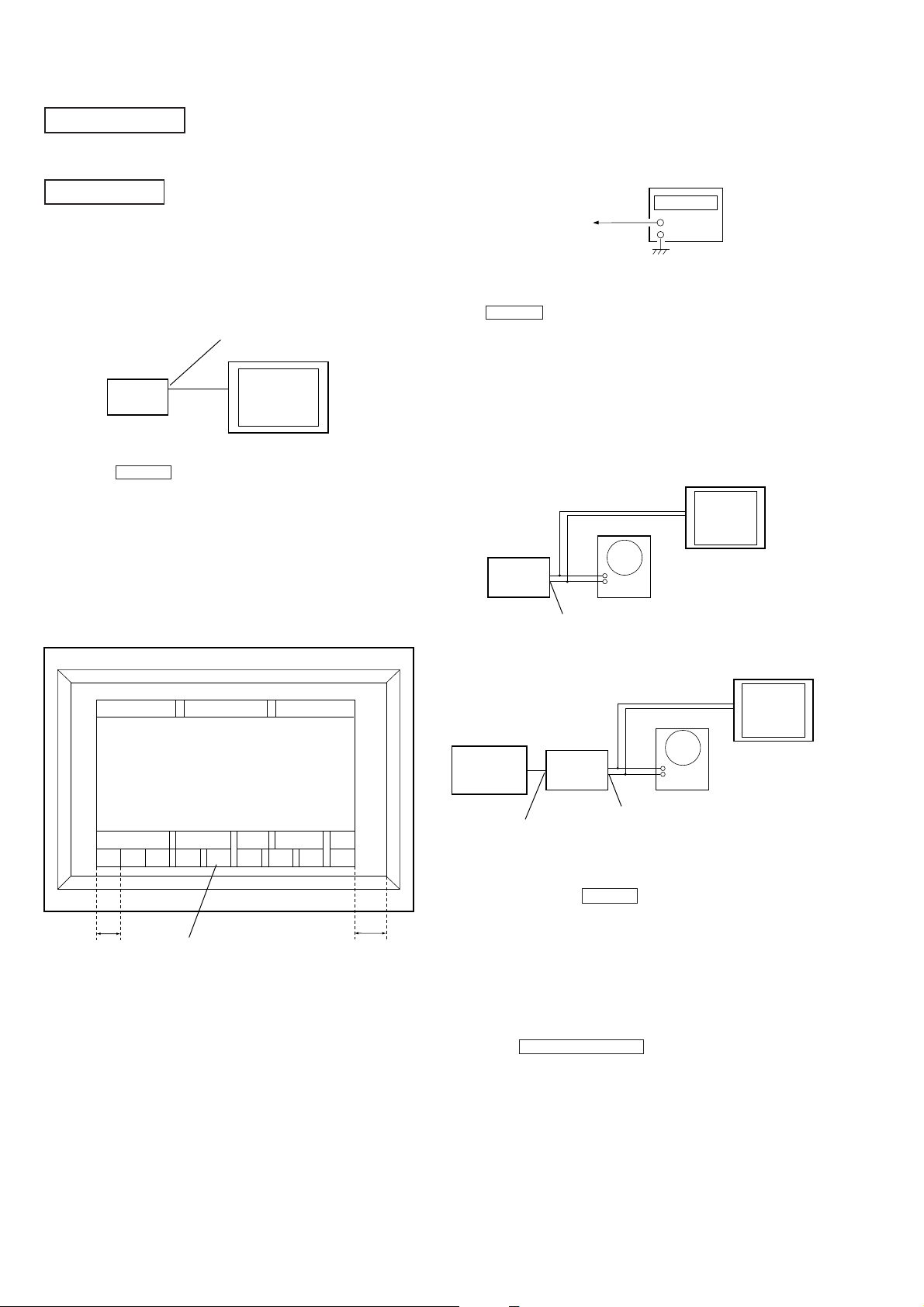
SECTION 5
r
ELECTRICAL ADJUSTMENT
TUNER SECTION
No adjustment is needed due to a tuner unit (TU401).
OSD SECTION
OSD WIDTH Adjustment
Note: Perform “ALL CLEAR” before this adjustment.
(Refer to Servicing note on page 4)
Connection:
MONITOR OUT
SET
Procedure:
1. Press the POWER button and turn ON the power.
2. The OSD function frame will be displayed on the monitor. This
screen will disappear in a few seconds automatically when the
input of codes using the remote commander stops.
If it disappears during adjustments, move the cursor of the remote commander supplied as an accessory. The screen will appear again.
3. While watching the monitor screen, adjust CT201 of the OSD
(V) board so that the following adjustment standard is satisfied.
monitor screen
Monitor
OSD COLOR BURST Adjustment
Connection:
frequency counte
OSD (V) board
JW232
+
–
Procedure:
1. Without anything connected to the external input terminal, press
the POWER button and turn ON the power.
2. Adjust CT202 of the OSD (V) board so that the reading on the
frequency counter becomes 3.579545 MHz ± 10 MHz.
OSD PICTURE Adjustment
Connection:
Connection 1:
Vectorscope
set
MONITOR OUT
Connection 2:
Monitor
FUNCTION SOUND SETUP
F1
A
OSD function frame
INPUT SUB USER
FPFpF)F(F0
F=
F™
F+
B
Adjustment standard:
Adjust so that the width B becomes one and a half times of width A.
1.5A = B
NOTE:
Extra margin is provided in this adjustment in consideration of the
deviation of the screen according to the type of monitor used.
Consequently, the user is able to adjust the position of the screen
freely. (For details, refer to “Adjustment of OSD Screen Position”
in 1. Servicing note. Refer to page 4.)
Monitor
VTR etc.
VIDEO 1 IN
Vectorscope
set
MONITOR OUT
Procedure 1:
1. Without anything connected to the external input terminal (connection 1), press the POWER button and turn ON the power.
2. Check that the OSD function frame screen is displayed on the
monitor. If no OSD function frame screen is displayed, move
the cursor button of the remote commander supplied as an accessory provided to display the screen.
3. Observe the vectorscope, and adjust RV201 of the OSD (V) board
so that the light dots converge in the BLUE area.
4. Connect a dynamic picture video device to the external input
terminal (VIDEO 1 IN jack) of this unit (Connection 2).
5. Press the VIDEO FUNCTION button and set the input source
to VIDEO 1.
6. Move the cursor of the remote commander supplied as an accessory provided, and display the OSD function frame.
7. Observe the vectorscope. Check that the light dots in the BLUE
range and the light dots adjusted at 3 are coinciding.
8. If they do not coincide, disconnect the external video device,
and adjust RV201 of the OSD (V) board again.
9. If the light dots when an external video device is connected and
not connected coincide, it indicates the end of the adjustment.
— 28 —
Page 8
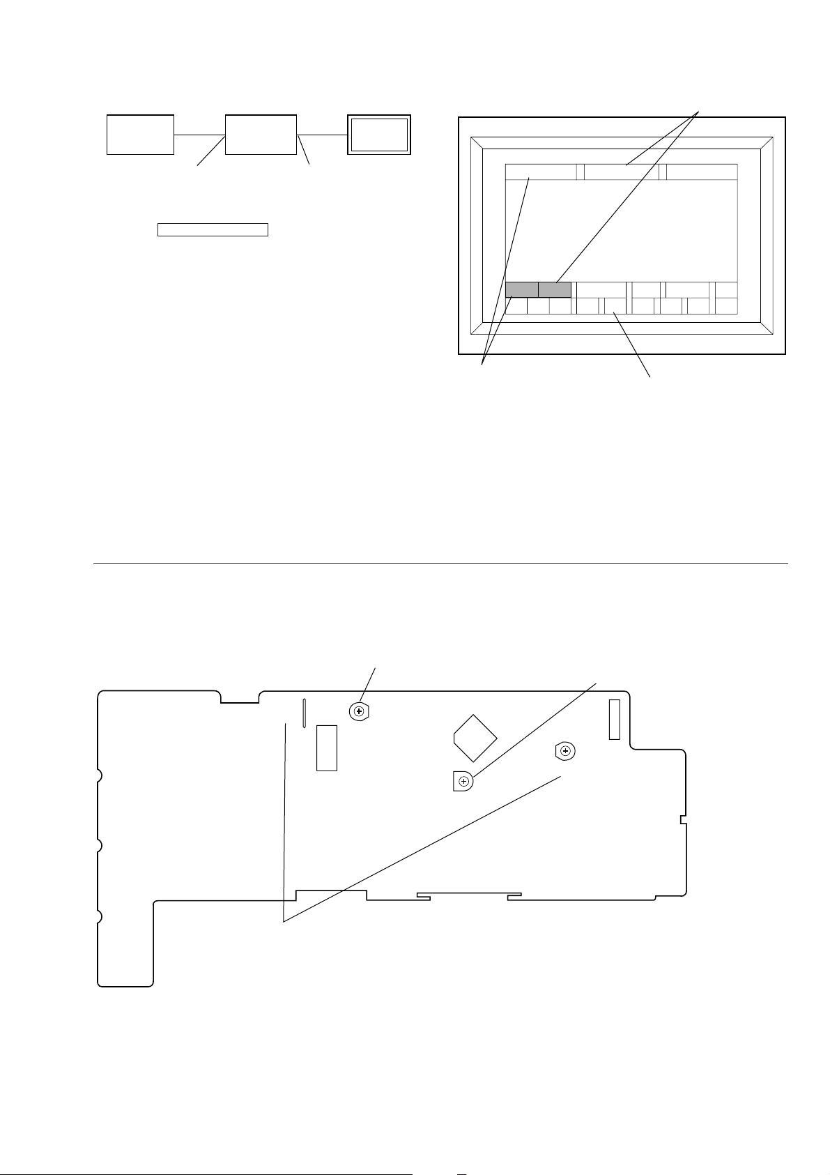
Procedure 2: (When no vectorscope is used)
monitor screen
FUNCTION SOUND SETUP
INPUT SUB USER
F™
F+
F=
FPFpF)F(F0
F1
OSD function frame
Blue area
Green area
Connection:
VTR etc. Monitor
VIDEO 1 IN
set
MONITOR OUT
Monitor
1. Connect a dynamic picture video device to the VIDEO 1 IN
jack of the unit.
2. Press the VIDEO FUNCTION button, and set the input source
to VIDEO 1.
3. Move the cursor of the remote commander supplied as an accessory provided, and display the OSD function frame.
4. Take note of the blue and green screens at the bottom left of the
OSD function frame.
5. Disconnect the video device connected at 1.
6. Adjust RV201 of the OSD (V) board so that the blue and green
parts at the bottom left of the OSD function frame to the same
color as the images checked at 4.
Note) Perform this adjustment when disconnecting the external video de-
vice. If the external video device is connected, there is no meaning
in performing this adjustment due to the use of the color burst of the
external device instead of the internal sync signal.
Adjustment Location
[OSD (V) BOARD] (Component side)
OSD COLOR BURST
JW232
OSD WIDTH
OSD PICTURE
IC215
CT201
CNP202
CT202
IC205
RV201
— 29 —
Page 9

6-1. IC PIN FUNCTIONS
• IC103 Mode controller (MB90673PF)
Pin No. Pin Name
MBUS-V2
1
MBUS-MON
2
MBUS-STATUS-OUT
3
—
4
—
5
—
6
LED STANDBY
7
LED SURR
8
LED TONE
9
10
11
12
13
14
15
16
17
18
19
20
21
22
23
24
25
26
27
28
29
30
31
32
33
34
35
36
37
38
39
40
LED INDEX
VSS
LED CD
LED DAT/MD
LED TAPE
LED TV
LED LD
LED V3
LED V2
LED V1
RX (SIN)
TX (SOUT)
BUSY
FL CLEAR
FL DATA
FL CLK
FL LAT
SIRCS
VCC (A)
+AVR
–AVR
GND (D)
AD KEY IN 1
AD KEY IN 2
VSS (D)
AD KEY IN 3
AD KEY IN 4
AD KEY IN 5
AD VERSION
VOL +
VOL –
SECTION 6
DIAGRAMS
I/O
–
Not used
–
Not used
–
Not used
–
Not used
–
Not used
–
Not used
O
STANDBY indicator drive signal output
O
SURROUND indicator drive signal output
O
TONE indicator drive signal output
O
INDEX indicator drive signal output
–
Ground
O
CD indicator drive signal output
O
DAT/MD indicator drive signal output
O
TAPE indicator drive signal output
O
TV indicator drive signal output
O
LD indicator drive signal output
O
VIDEO3 indicator drive signal output
O
VIDEO2 indicator drive signal output
O
VIDEO1 indicator drive signal output
O
Serial data output to OSD controller
I
Serial data input from OSD controller
I/O
Serial clock input/output with OSD controller
O
FL clear signal output to FL driver “H” : active
O
FL data output to FL diver
O
FL clock output to FL diver
O
FL latch output to FL driver “H” : active
I
Remote control signal input
–
+5V power supply (Back-up)
I
Reference voltage input (+) (+5V)
I
Reference voltage input (–) (Ground)
–
Ground
I
Key input 1
I
Key input 2
–
Ground
I
Key input 3
I
Key input 4
I
Key input 5
I
AD version setting input
O
Volume motor control signal output
O
Volume motor control signal output
Function
Function
• Abbreviation
OSD : On Screen Display
FL : Fluorescent indicator tube
— 30 —
Page 10

Pin No. Pin Name
41
42
43
44
45
46
47
48
49
50
51
52
53
54
55
56
57
58
59
60
61
62
63
64
65
66
67
68
69
70
71
72
73
74
75
76
77
78
79
80
MODE0
MODE1
MODE2
STANBY
STOP
U-RESET
U-SREQ
U-MREQ
U-DATA
U-CLOCK
(GND)
AUBUS IN
AUBUS OUT
(GND)
FUNCTION-B
FUNCTION-A
UP/DOWN-B
UP/DOWN-A
LEFT/RIGHT-B
LEFT/RIGHT-A
—
RESET
VSS (D)
XO
XI
VCC (D)
LED TUNER
LED PHONO
LED MUTE
LED LEARNING
LED D. PASS
LED INPUT
LED VOL
LED BASS B
SP-A
SP-B
PW-SW
—
—
MBUS-V1
I/O
I
Mode setting pin (Fixed at “H”)
I
Mode setting pin (Fixed at “H”)
I
Mode setting pin (Fixed at “L”)
I
Stanby signal input (Fixed at “H”)
I
STOP signal input “L” : active
O
Reset output to system controller “L” : reset
I
Slave data request signal input from system controller
O
Master request signal output to system controller
O
Master data output to system controller
O
Master clock output to system controller
–
Ground
–
Not used
–
Not used
–
Ground
–
Not used
–
Not used
–
Not used
–
Not used
–
Not used
–
Not used
–
Not used (Ground)
I
Reset signal input “L” : reset
–
Ground
O
Clock output (4MHz)
I
Clock input (4MHz)
–
+5V power supply (Back-up)
O
TUNER indicator drive signal output
O
PHONO indicator drive signal output
O
MUTE indicator drive signal output
O
LEARNING indicator drive signal output
O
DIRECT PASS indicator drive signal output
O
INPUT indicator drive signal output
O
Volume indicator drive signal output “H” : active
O
Bass boost indicator drive signal output “H” : active
O
Speaker select control signal output
O
Speaker select control signal output
I
Power on detect signal input
–
Not used
–
Not used
–
Not used
Function
Function
— 31 —
Page 11
• IC205 OSD (MB90095PF-G-186-BND)
Pin No.
1
2
3
4
5
6
7
8
9
10
11
12
13
14
15
16
17
18
19
20
21
22
23
24
25
26
27
28
Pin Name
YIN
CIN
VIN
AVCC
FSCO
VBLK
VCC
EXS
XS
HSYNC
VSYNC
EXHSYN
EXVSYN
GND
EXD
XD
VOB
VOC 2
VOC 1
VOC 0
TEST
S. CLK
S. DATA
CS
VOUT
COUT
YOUT
AGND
I/O
I
Luminous signal input for superimpose displays
I
Chroma signal input for superimpose displays
I
Composite signal input for superimpose displays
–
Power supply (+5V) (Analog)
O
Color burst phase signal output
O
Vertical blanking period output (Not used)
–
Power supply (+5V)
I
External circuit of the clock generator for color burst signals (14.3MHz)
O
External circuit of the clock generator for color burst signals (Not used)
O
H. SYNC/COMPOSIT SYNC singal output
O
V. SYNC signal output (Not used)
I
External H. SYNC signal input
I
External V. SYNC signal input
–
Ground
I
External circuit of the display dot clock generator
O
External circuit of the display dot clock generator
O
Character and background period signal output (Not used)
O
Chroma signal output (Not used)
O
Chroma signal output (Not used)
O
Chroma signal output (Not used)
I
Test pin (Fixed at “H”)
I
Shift clock input for serial transmission
I
Serial data input
I
Chip select input
O
Composite video signal output
O
Chroma signal output
O
Luminous signal output
–
Ground (Analog)
Function
• Abbreviation
OSD : On Screen Display
— 32 —
Page 12
• IC209 OSD Controller (MB90672PF-G-125-BND)
Pin No.
1, 2
3 to 6
7
8
9
10
11
12
13
14
15
16
17
18
19
20
21
22
23
24
25
26
27
28
29
30
31
32
33
34
35
36
37
38
39
40
Pin Name
AD14, AD15
A16 to A19
PCE
PCLK
PDATA OUT
PDATA IN
GND
ALE
RDX
WRLX
WRHX
MONITOR
VIDEO 2
STATUS-OUT
VIDEO 1
RX (SIN)
TX (SOT)
P PRES
TEST 1
DATA (OSD)
CLK (OSD)
LAT (OSD)
—
AVCC
AVR +
AVR –
AVSS
VOLA/D
PREADY
GND
PSTATUS
OK
MEMORY FULL
BACK UP NG
NG
P-IR
I/O
Address bus and data bus input/output
I/O
Address bus output
O
Chip Enable output to RC controller (For communication using personal computers)
O
Clock output to RC controller (For communication using personal computers)
O
Data output to RC controller (For communication using personal computers)
O
Data input from RC controller (For communication using personal computers)
I
Ground
–
Address latch enable output
O
Read strobe output to data bus
O
O
Write strobe output to data bus
O
Control-S input (Monitor) (Fixed at “L”)
I
Control-S input (VIDEO 2)
I
Control-S status output
O
Control-S input (VIDEO 1)
I
Serial data input from mode control (U-ART0 reception)
I
Serial data output to mode control (U-ART0 transmission)
O
Reset output (For communication using personal computers)
O
Test port (Not used)
O
Serial data output to OSD
O
Serial clock output to OSD
O
Latch output to OSD
O
Not used
–
Power supply (+5.6V)
–
Power supply (+5V)
–
–
Ground
–
Volume control signal input (Not used)
I
Learning code reception ready signal input “L” : nothing
I
Ground
–
Infrared rays transmission data status signal input from to RC controller
I
Learning OK signal input from RC controller
I
Memory full signal input from RC controller
I
Back up NG signal input from RC controller
I
Learning NG signal input from RC controller
I
Input to the integral calculus circuit of the remote control reception signal
I
Function
• Abbreviation
RC: Remote Commander
OSD: On Screen Display
— 33 —
Page 13
Pin No.
41
42
43
44
45
46
47
48
49
50
51
52
53
54
55
56
57
58
59
60
61
62
63
64
65
66
67 to 100
Pin Name
MODE 0
MODE 1
MODE 2
HSTX
STOP
IR-IN (A6)
—
—
AUBUS IN
V. SIGNAL
SIRCS-IN
VD
AUBUS OUT
F. SW
VIDEO-MUT
—
—
—
—
IR ON/OFF
BUSY
RESET
GND
XO
XI
VCC
AD00 to AD13
I/O
Mode setting (Fixed at “H”)
I
Mode setting (Fixed at “L”)
I
Mode setting (Fixed at “L”)
I
Hardware standby (Fixed at “H”)
I
Request input of reset interrupt
I
IR sensor remote control input (Not used)
I
Not used
–
Not used
–
S-LINK control A1 signal input
I
H-sync switching signal input
I
SIRCS signal input
I
PAL: 60 [flame/s]/ NTSC: 50 [flame/s] signal detect VD input
I
S-LINK control A1 signal output
O
To control output into monitor (Not used)
O
Image mute output (Not used)
O
Not used
–
Not used
–
Not used
–
Not used
–
IR remote control ON/OFF output “H” off
O
Input/output to communicate with the mode control
I/O
Reset signal input
I
Ground
–
Clock (4 MHz)
O
Clock (4 MHz)
I
Power supply (+5.6V)
–
Address bus and data bus input/output
I/O
Function
— 34 —
Page 14

• IC215 RC Controller (LC86F5864A-5F53)
Pin No.
1
2
3
4
5
6
7
8
9
10
11
12
13
14
15
16
17
18
19
20
21
22
23
24
25
26
27
28
29
30
31
32
33
34
35
36
37
38
39
40
Pin Name
P70/INT0
P71/INT1
P72/INT 2/TOIN
P73/INT 3/TOIN
P30
P31
P32
P33
P34
P35
P36
P37
P40
P41
P42
P43
P44
P45
P46
P47
P50/SDA
P51/SCL
VSS2
VDD2
P20/SDA
P21/SCL
P22/TXD
P23/PXD
P24/UCLK
P25
P26
P27
P00
P01
P02
P03
P04
P05
P06
P07
I/O
I
Chip enable input from OSD controller
I
Chip enable input (For on-board) (Not used)
I
Not used (Fixed at “L”)
I
SIRCS signal input
I
Power supply normality signal input
O
Infrared rays transmission data status signal output to OSD controller “L” nothing
O
Learning NG signal output to OSD controller
O
Back-up NG signal output to OSD controller
O
Memory-full signal output to OSD controller
O
Learning OK signal output to OSD controller
O
Data reception ready signal output to OSD controller
O
Not used (Fixed at “L”)
O
Not used (Fixed at “L”)
O
Not used (Fixed at “L”)
O
Not used (Fixed at “L”)
O
Not used (Fixed at “L”)
O
Not used (Fixed at “L”)
O
Not used (Fixed at “L”)
O
Not used (Fixed at “L”)
O
Not used (Fixed at “L”)
O
Not used (Fixed at “L”)
O
Not used (Fixed at “L”)
–
Ground
–
+5V power supply
O
Not used (Fixed at “L”)
O
Not used (Fixed at “L”)
O
Not used (Fixed at “L”)
O
Not used (Fixed at “L”)
O
Not used (Fixed at “L”)
O
Not used (Fixed at “L”)
O
Not used (Fixed at “L”)
O
Not used (Fixed at “L”)
O
Not used (Fixed at “L”)
O
Not used (Fixed at “L”)
O
Not used (Fixed at “L”)
O
Not used (Fixed at “L”)
O
Not used (Fixed at “L”)
O
Not used (Fixed at “L”)
O
Not used (Fixed at “L”)
O
Not used (Fixed at “L”)
Function
• Abbreviation
RC: Remote Commander
OSD: On Screen Display
— 35 —
Page 15
Pin No.
41
42
43
44
45
46
47
48
49
50
51
52
53
54
55
56
57
58
59
60
61
62
63
64
Pin Name
P10/SOO
P11/SI0/SB0
P12/SCKO
P13/SO1
P14/SI1
P15/SCK1
P16/BUZ
P17/PWM
TEST1
RES
XT1/P74
XT2
VSS1
CF1
CF2
VDD1
P80/AN0
P81/AN1
P82/AN2
P83/AN3
P84/AN4
P85/AN5
P86/AN6
P87/AN7
I/O
O
Serial data output to OSD controller
I
Serial data input to OSD controller
I
Serial clock input from OSD controller
–
Serial data output (For on-board) (Not used)
I
Serial data input (For on-board) (Not used)
I
Serial clock input (For on-board) (Not used)
O
Not used (Fixed at “L”)
O
SIRCS signal output (Carrier = PWM output)
O
Not used
I
Reset input “L” reset
–
Not used (Fixed at “H”)
–
Not used
–
Ground
I
Clock input (6MHz)
O
Clock output (6MHz)
–
+5V power supply
I
Not used (Fixed at “L”)
I
Not used (Fixed at “L”)
I
Not used (Fixed at “L”)
I
Not used (Fixed at “L”)
I
Not used (Fixed at “L”)
I
Not used (Fixed at “L”)
I
Not used (Fixed at “L”)
I
Not used (Fixed at “L”)
Function
• Abbreviation
OSD: On Screen Display
— 36 —
Page 16
• IC3104 A/D Converter (CXD8681M-TP)
Pin No. Pin Name
VRL+
1
VRL–
2
VCML
3
AINL+
4
AINL–
5
ZCAL
6
VD
7
DGND
8
CAL
9
10
11
12
13
14
15
16
17
18
19
20
21
22
23
24
25
26
27
28
RST
SMODE2
SMODE1
LRCK
SCLK
SDATA
FSYNC
MCLK
CMODE
SEL24/20
TEST
BGND
AGND
VA
AINR–
AINR+
VCMR
VRR–
VRR+
I/O
O
O
O
I
I
I
–
–
O
I
I
I
I/O
I/O
O
I/O
I
I
I
I
–
–
–
I
I
O
O
O
Function
Function
L-ch reference voltage (+) output (+3.75V)
L-ch reference voltage (–) output (+1.25V)
L-ch common voltage (+) output (+2.5V)
L-ch analog voltage (+) input
L-ch analog voltage (–) input
Zero calibraton input (Fixed at “H”)
+5.5V power supply (Digital)
Ground (Digital)
Calibration status signal output
Reset input “L” : reset
Serial interface mode selection input (Fixed at “L”)
Serial interface mode selection input (Fixed at “L”)
L/R channel selection clock input/output
Serial data clock input/output
Serial data output
Frame sync clock input/output (Fixed at “H”)
Master clock input (12.288MHz)
Master clock selection input “L” : MCLK : 256Fs, “H” : MCLK : 384Fs (Fixed at “L”)
Output data range selection input “L” : 20 bit, “H” ; 24 bit (Fixed at “H”)
Test pin (Fixed at “L”)
Ground
Ground (Analog)
+5V power supply (Analog)
R-ch analog (–) input
R-ch analog (+) input
R-ch common voltage output (+2.5V)
R-ch reference voltage (–) output (+1.25V)
R-ch reference voltage (+) output (+3.75V)
— 37 —
Page 17

• IC3308 DOLBY AC-3 demodulator (SN-PM4007A)
Pin No. Pin Name
GND
1
VDD
2
RESET
3
OSCON
4
DATA
5
MCK
6
MLTB
7
IDST
8
IDCK
9
10
11
12
13
14
15
16
17
18
19
20
21
22
23
24
25
26
27
28
29
30
31
32
33
34
35
36
37
38
39
40
41
42
43
44
45
46
47
48
49
50
IDO
TM0
ECCK
DEN
DRY
MSYC
TM1
A0
A1
A2
A3
A4
A5
TM2
TM3
XOUT
XIN
NEXT
GND
VDD
A6
A7
GND
VDD
A12
A14
WE
A13
A8
A9
GND
A11
OE
A10
D7
D6
D5
D4
D3
D2
D1
I/O
–
Ground
–
+5V power supply
I
System reset input “L” : reset
I
Oscillation control signal input “H” : ON (Fixed at “H”)
I
Test pin (Fixed at “L”)
I
Test pin (Fixed at “L”)
I
Test pin (Fixed at “L”)
O
Test pin (Not used)
O
Test pin (Not used)
O
Test pin (Not used)
I
Test pin (Fixed at “L”)
O
Test pin (Not used)
O
Test pin (Not used)
O
Test pin (Not used)
O
Test pin (Not used)
I
Test pin (Fixed at “L”)
O
Address data output to SRAM
O
Address data output to SRAM
O
Address data output to SRAM
O
Address data output to SRAM
O
Address data output to SRAM
O
Address data output to SRAM
I
Test pin (Fixed at “L”)
I
Test pin (Fixed at “L”)
O
Test pin (Not used)
I
Test pin (Fixed at “L”)
I
Test pin (Fixed at “L”)
–
Ground
–
+5V power supply
O
Address data output to SRAM
O
Address data output to SRAM
–
Ground
–
+5V power supply
O
Address data output to SRAM
O
Address data output to SRAM
O
Write enable signal output to SRAM “L” : active
O
Address data output to SRAM
O
Address data output to SRAM
O
Address data output to SRAM
–
Ground
O
Address data output to SRAM
O
Output enable output to SRAM
O
Address data output to SRAM
I/O
Data bus input/output with SRAM
I/O
Data bus input/output with SRAM
I/O
Data bus input/output with SRAM
I/O
Data bus input/output with SRAM
I/O
Data bus input/output with SRAM
I/O
Data bus input/output with SRAM
I/O
Data bus input/output with SRAM
Function
Function
— 38 —
Page 18

Pin No. Pin Name
51
52
53
54
55
56
57
58
59
60
61
62
63
64
65
66
67
68
69
70
71
72
73
74
75
76
77
78
79
80
81
82
83
84
85
86
87
88
89
90
91
92
93
94
95
96
97
98
99
100
D0
VDD
GND
TI1
VIN
VOUT
TI2
TI3
TLD8
TCK
TRP
TD0
PD0
TI4
PDDI5
MUTO
TI5
VLDY
DASYO
DAOUT
DAIN
DAIN
TI8
C2F1
C2F0
C1F1
C1F0
MUTI
VDD
GND
AVDD
CPIN
CMIN
AGND
TM4
VDD
DIN
DOUT
DOUTB
C9M
GND
WINGT
SYST0
SYST1
ADST0
ADST1
TM5
BUNRI
AGND
AVDD
Function
I/O
I/O
Data bus input/output with SRAM
–
+5V power supply
–
Ground
I
Test pin (Fixed at “H”)
I
VCXO input (18.432MHz)
O
VCXO output (18.432MHz)
I
Test pin (Fixed at “L”)
I
Test pin (Fixed at “L”)
I
Test pin (Fixed at “L”)
I
Test pin (Fixed at “L”)
O
Test pin (Not used)
O
Test pin (Not used)
O
Output of internal phase comparator (3 state)
I
Test pin (Fixed at “L”)
I
PDO output control input “L” : output ON
O
Mute signal output “H” : mute
I
Test pin (Fixed at “L”)
O
Test pin (Not used)
O
Test pin (Not used)
O
Digital-out signal output (Serial data stream output)
I
Dgital external input Through out to DAOUT when DASEL is “H” (Not used)
I
Digital-out selection input (Fixed at “L”)
I
Test pin (Fixed at “L”)
O
C2 error correction state display Outputs if corrected properly (Not used)
O
C2 error correction state display Outputs number of errors at C2 (Not used)
O
C2 error correction state display Outputs whether error is present at C1 (Not used)
O
C2 error correction state display Outputs number of errors at C1 (Not used)
I
Muting input “H” mute
–
+5V power supply
–
Ground
–
+5V power supply (Analog)
I
Comparator input (+) (QPSK input)
I
Comparator input (–)
–
Ground (Analog)
I
Test pin (Fixed at “L”)
–
+5V power supply
I
Test pin (Fixed at “L”)
O
Comparate output
O
Comparate inverted output
O
9.216MHz output (Not used)
–
Ground
O
Test pin (Not used)
O
Test pin (Not used)
O
Test pin (Not used)
O
Test pin (Not used)
O
Test pin (Not used)
I
Test pin (Fixed at “L”)
I
Test pin (Fixed at “L”)
–
Ground (Analog)
–
+5V power supply (Analog)
Function
— 39 —
Page 19
• IC3311 Digital Audio Interface Receiver (CXD8521M)
10
11
12
13
14
15
16
17
18
19
20
21
22
23
24
I/O
DIN1
1
DIN2
2
E/DOUT
3
VDD
4
R
5
VIN
6
VCO
7
GND
8
CKSEL
9
XMODE
AVOCK
TST1
TST2
SCLK
XLAT
SWDT
SRDT
DQSY
CKOUT
FS128
BCK
LRCK
DA TAO
EROR
I
Data input with built-in amplifier (Responding to the coaxial optical module)
I
Data input (Responding to the optical module)
O
Emphasis, input bi-phase, validity flag output
–
Power supply (+5V)
I
VCO gain control input (Fixed at “H”)
I
VCO freerunning frequency setting input
O
LPF setting of PLL (Fixed at “L”)
–
Ground
I
System clock select input (384fs, 512fs) (Connected to the power supply.)
I
Reset input
I
Clock input for preventing PLL lock failure
I
Test input (Normally “L”)
I
I
Microcomputer IF clock input
I
Microcomputer IF latch/chip enable input
I
Microcomputer IF write data input
O
Microcomputer IF read data output
O
Microcomputer IF Sub-Q sync and ID sync output (Not used)
O
VCO clock output (Freerunning, 384fs, 512fs) (Not used)
O
128fs clock output (Not used)
O
Bit clock output
O
L/R clock output
O
Audio data output
O
PLL lock error mute output
Function
FunctionPin No. Pin Name
• Abbreviation
VCO: Voltage Controlled Oscillator
PLL: Phase Locked Loop
— 40 —
Page 20

• IC3410 DOLBY AC-3 decoder (DSP56009FJ88)
Pin No. Pin Name
AGND
1
MCS0
2
MA15
3
MA14
4
MA13
5
AVCC
6
MA12
7
AGND
8
QVCC
9
10
11
12
13
14
15
16
17
18
19
20
21
22
23
24
25
26
27
28
29
30
31
32
33
34
35
36
37
38
39
40
QGND
MA11
MA10
MA9
MA8
AGND
MA7
AVCC
MA6
MA5
MA4
AGND
MA3
MA2
MA1
MA0
SCK/SCL
EXTAL
QVCC
QGND
PINIT
PGND
PCAP
PVCC
SGND
MISO/SDA
RESET
MODA/IRQA
MODB/IRQB
MODC/NMI
SVCC
I/O
–
Address buffer ground
O
Chip select 0 output to S-RAM (Not used)
O
O
Address data output to S-RAM (Not used)
O
–
Address bus buffer power supply (+5V)
O
Address data output to S-RAM(Not used)
–
Ground for address bus buffer
–
Power supply for internal logic (+5V)
–
Ground for internal logic
O
O
Address data output to S-RAM (Not used)
O
O
Ground for address bus buffer
–
Address data output to S-RAM (Not used)
O
Power supply for address bus buffer (+5V)
–
O
Address data output to S-RAM (Not used)
O
O
Ground for address bus buffer
–
O
O
Address data output to S-RAM (Not used)
O
O
SPI serial clock signal input from system controller
I
External frequency input (3 MHz)
I
Power supply for internal logic (+5V)
–
Ground for internal logic
–
PLL initialize input (Fixed at “L”)
I
Ground for PLL
–
PLL filter input (Connected to 0.01 µF capacitor)
I
Power supply for PLL (+5V)
–
Ground for serial port
–
Master data signal input from system controller
I
Reset signal input from system controller
I
Mode select A (Fixed at “H”)
I
Mode select B (Fixed at “L”)
I
Mode select C (Fixed at “H”)
I
Power supply for serial port (+5V)
–
Function
Function
• Abbreviation
PLL: Phase Locked Loop
— 41 —
Page 21
Pin No. Pin Name
41
42
43
44
45
46
47
48
49
50
51
52
53
54
55
56
57
58
59
60
61
62
63
64
65
66
67
68
69
70
71
72
73
74
75
76
77
78
79
80
MOSI/HA0
SS/HA2
HREQ
SGND
SDO2
SDO1
SDO0
SVCC
SCKT
WST
SCKR
QGND
QVCC
SGND
WSR
SDI1
SDI0
DSO
DSI/OS0
DSCK/OS1
DR
MD7
MD6
MD5
MD4
DGND
MD3
MD2
MD1
DVCC
MD0
DGND
GPIO3
GPIO2
GPIO1
GPIO0
MRD
MWR
MA15/MCS1
MA16/MCS2/MCAS
Function
I/O
O
Master data signal output to system controller
I
SPI slave select signal input from system controller
I
Host request signal input from system controller
–
Ground for serial port
O
Audio serial data 2 signal output (Not used)
O
Audio serial data 1 signal output
O
Audio serial data 0 signal output
–
Power supply for serial port (+5V)
O
Serial clock transmission
O
Word select transmission
I
Serial clock reception
–
Ground for internal logic
–
Power supply for internal logic (+5V)
–
Ground for serial port
I
Word select reception
I
Audio serial data 1 signal input
I
Audio serial data 0 signal input
O
Debug serial signal output (Not used)
I
Debug serial signal input (Not used)
I
Debug serial clock signal input (Not used)
I
Debug request input (Fixed at “H”)
I/O
I/O
Data input/output with S-RAM (Not used)
I/O
I/O
Ground for data bus buffer
–
I/O
Data input/output with S-RAM (Not used)
I/O
I/O
Power supply for data bus buffer (+5V)
–
Data input/output with S-RAM (Not used)
I/O
Ground for data bus buffer
–
I/O
I/O
General DSP input/output (Not used)
I/O
I/O
Write strobe signal output to S-RAM (Not used)
O
Read strobe signal output to S-RAM (Not used)
O
Low address strobe signal output to S-RAM (Not used)
O
Column address strobe signal output to S-RAM (Not used)
O
Function
— 42 —
Page 22
• IC3412 DOLBY Surround Digital Signal Processor (SSP424023FJ88)
Pin No. Pin Name
AGND
1
MCS0
2
MA15
3
MA14
4
MA13
5
AVCC
6
MA12
7
AGND
8
QVCC
9
10
11
12
13
14
15
16
17
18
19
20
21
22
23
24
25
26
27
28
29
30
31
32
33
34
35
36
37
38
39
40
QGND
MA11
MA10
MA9
MA8
AGND
MA7
AVCC
MA6
MA5
MA4
AGND
MA3
MA2
MA1
MA0
SCK/SCL
EXTAL
QVCC
QGND
PINIT
PGND
PCAP
PVCC
SGND
MISO/SDA
RESET
MODA/IRQA
MODB/IRQB
MODC/NMI
SVCC
I/O
–
Address buffer ground
O
Chip select 0 output to S-RAM (Not used)
O
O
Address data output to S-RAM
O
–
Address bus buffer power supply (+5V)
O
Address data output to S-RAM
–
Ground for address bus buffer
–
Power supply for internal logic (+5V)
–
Ground for internal logic
O
O
Address data output to S-RAM
O
O
Ground for address bus buffer
–
Address data output to S-RAM
O
Power supply for address bus buffer (+5V)
–
O
Address data output to S-RAM
O
O
Ground for address bus buffer
–
O
O
Address data output to S-RAM
O
O
SPI serial clock signal input from system controller
I
External frequency input (3 MHz)
I
Power supply for internal logic (+5V)
–
Ground for internal logic
–
PLL initialize input (Fixed at “L”)
I
Ground for PLL
–
PLL filter input (Connected to 0.01 µF capacitor)
I
Power supply for PLL (+5V)
–
Ground for serial port
–
Master data signal input from system controller
I
Reset signal input from system controller
I
Mode select A (Fixed at “H”)
I
Mode select B (Fixed at “L”)
I
Mode select C (Fixed at “H”)
I
Power supply for serial port (+5V)
–
Function
Function
• Abbreviation
PLL: Phase Locked Loop
— 43 —
Page 23
Pin No. Pin Name
41
42
43
44
45
46
47
48
49
50
51
52
53
54
55
56
57
58
59
60
61
62
63
64
65
66
67
68
69
70
71
72
73
74
75
76
77
78
79
80
MOSI/HA0
SS/HA2
HREQ
SGND
SDO2
SDO1
SDO0
SVCC
SCKT
WST
SCKR
QGND
QVCC
SGND
WSR
SDI1
SDI0
DSO
DSI/OS0
DSCK/OS1
DR
MD7
MD6
MD5
MD4
DGND
MD3
MD2
MD1
DVCC
MD0
DGND
GPIO3
GPIO2
GPIO1
GPIO0
MRD
MWR
MA15/MCS1
MA16/MCS2/MCAS
I/O
O
Master data signal output to system controller
I
SPI slave select signal input from system controller
I
Host request signal input from system controller
–
Ground for serial port
O
Audio serial data 2 signal output
O
Audio serial data 1 signal output
O
Audio serial data 0 signal output
–
Power supply for serial port (+5V)
O
Serial clock transmission
O
Word select transmission
I
Serial clock reception
–
Ground for internal logic
–
Power supply for internal logic (+5V)
–
Ground for serial port
I
Word select reception
I
Audio serial data 1 signal input
I
Audio serial data 0 signal input
O
Debug serial signal output (Not used)
I
Debug serial signal input (Not used)
I
Debug serial clock signal input (Not used)
I
Debug request input (Fixed at “H”)
I/O
I/O
Data input/output with S-RAM
I/O
I/O
Ground for data bus buffer
–
I/O
Data input/output with S-RAM
I/O
I/O
Power supply for data bus buffer (+5V)
–
Data input/output with S-RAM
I/O
Ground for data bus buffer
–
I/O
General DSP input/output (Not used)
I/O
I/O
General DSP output to system controller
O
Write strobe signal output to S-RAM
O
Read strobe signal output to S-RAM
O
Low address strobe signal output to S-RAM (Not used)
O
Column address strobe signal output to S-RAM
O
Function
Function
— 44 —
Page 24

• IC3413 System Controller (MB90641APF-G-101-BND)
Pin No. Pin Name
RF ERR
1
RF RESET
2
STOP
3
RDATA
4
WDATA
5
DIRLAT
6
DIRCLK
7
DIRERR
8
ANG/DIG
9
10
11
12
13
14
15
16
17
18
19
20
21
22
23
24
25
26
27
28
29
30
31
32
33
34
35
36
37
38
39
40
41
42
43
44
45
46
47
48
49
50
A/DINT
VSS
HREQ
SS
MOSI
RESET
MISO
CLOCK
HREQ
SS
MOSI
RESET
MISO
VCC
CLOCK
D/AINT
D/ALAT
C
D/ACLK
D/ADATA
—
—
—
—
VCC
VCC
VSS
VSS
LOW FRQ LED
GAIN FRONT 8DB
GAIN FRONT 4DB
GAIN FRONT 2DB
VSS
—
—
—
—
—
STOP
MD0
MD1
I/O
I
Error input from DOLBY AC-3 demodulator “H” : error
O
Reset output to DOLBY AC-3 demodulator “L” : reset
I
Power supply failure detection input
I
Data read signal input from CXD8521M
O
Data write signal output to CXD8521M
O
Latch output to CXD8521M
O
Clock output to CXD8521M
I
Error signal input from CXD8521M “H” : error
O
Analog/Digital switching, Digital at “H”
O
Initialize output to A/D converter
–
Ground
O
Host request signal output to DSP56009FJ88
O
SPI slave select signal output to DSP56009FJ88
O
Master data signal output to DSP56009FJ88
O
Reset signal output to DSP56009FJ88 “L” : reset
I
Master data signal input from DSP56009FJ88
O
SPI serial clock output to DSP56009FJ88
O
Host request signal output to SSP424023FJ88
O
SPI slave select signal output to SSP424023FJ88
O
Master data signal output to SSP424023FJ88
O
Reset signal output to SSP424023FJ88 “L” : reset
I
Master data signal input from SSP424023FJ88
–
+5V power supply
O
SPI serial clock output to SSP424023FJ88
O
Initialize output to CXD8505BQ “L” : initialize
O
Latch output to CXD8505BQ
–
Connect to Capacitor
O
Clock output to CXD8505BQ
O
Data output to CXD8505BQ
O
Initialize output “L” : initialize (Not used)
–
Not used
–
Not used
–
Not used
–
+5V power supply
–
+5V power supply
–
Ground
–
Ground
I
Low frequency LED signal input from SSP424023FJ88
O
Front speaker 8dB gain signal output
O
Front speaker 4dB gain signal output
O
Front speaker 2dB gain signal output
–
Ground
–
Not used
–
Not used
–
Not used
–
Not used
–
Not used
I
Power supply failure detection input
I
Mode select input (Fixed at “H”)
I
Mode select input (Fixed at “H”)
Function
Function
— 45 —
Page 25

Pin No. Pin Name
51
52
53
54
55
56
57
58
59
60
61
62
63
64
65
66
67
68
69
70
71
72
73
74
75
76
77
78
79
80
81
82
83
84
85
86
87
88
89
90
91
92
93
94
95
96
97
98
99
100
MD2
STANDBY
—
DISPMR
DISPDATA
SLVDATA/REQ
DISPCLK
LAT
DAT A
CLK
DATAIN
AUTSTOP
STEREO
—
—
HIFI/ES
PROTEC
VIDEO-A
VIDEO-B
VIDEO-E
VIDEO-INH
FUNMUTE
TUNERMUTE
SURR-MUTE
AC-MUTE
RM-MUTE
RESET
RY-FRONT/A
RY-FRONT/B
RY FRONT
VSS
XIN
XOUT
VCC
RY-PREAMP
RY-CENTER
RY-REAR
RY-HP
RY-4/8
RY-POWER
—
—
—
RY-DIRECT-PASS
—
—
—
DIG-IN2
DIG-IN1
DIG-IN0
I/O
I
Mode select input (Fixed at “L”)
I
Power on detect input (Fixed at “H”)
–
Not used
I
Master request signal input from mode controller
I
Master data input from mode controller
O
Slave data request signal output to mode controller
I
Master clock input from mode controller
O
Latch output to ATT (Rear, Center, woofer)
O
Signal data output to ATT (Rear, Center, woofer)
O
Signal clock output to ATT (Rear, Center, woofer)
O
Serial data output to tuner
O
Auto stop signal output to tuner
O
Stereo ID output to tuner
–
Not used
–
Not used
–
Not used (Fixed at “H”)
O
Protector signal output
O
Video-input switching signal output
O
Video-input switching signal output
O
Video control E signal output
O
Video-out inhibit signal output “L” : inhibit
O
Function muting signal output “H” : mute
O
Tuner muting signal output “H” : mute
O
Surround muting signal output “H” : mute
O
Mute signal output to Front/Rear power amp
O
–20dB muting signal output “H” : mute
I
Reset signal input “L” : reset
O
Not used
O
Not used
O
Front speaker relay switching output “H” : ON
–
Ground
I
System clock input (4MHz)
O
System clock output (4MHz)
–
+5V power supply
–
Not used
O
Center speaker/Super woofer relay switching output “H” : ON
O
Rear speaker relay switching output “H” : ON
O
Headphones relay switching output “H” : ON
O
Not used
O
Power relay switching output “H” : ON
–
Not used
–
Not used
–
Not used
–
Direct pass relay switching output “H” : ON
–
Not used
–
Not used
–
Not used
O
Digital-input selection signal output
O
Digital-input selection signal output
O
Digital-input selection signal output
Function
— 46 —
Page 26

d
6-2. CIRCUIT BOARDS LOCATION
S-A-P board
REAR AMP board
SW board
PS board
SP (2F) board
AUDIO2F board
SURR-AUDIO2F boar
SECONDARY board
DISPLAY board
(including L.B SW board)
BALANCE board
VOLUME board
JOINT (OSD) board
OSD (V) board
JOINT (B) board
L.B SW board
VIDEO3 board
— 47 —
OSD (S) board
MEMORY board
Page 27

SP SW board
d
HEADPHONE board
AMP JOINT (F) board
AMP JOINT (B) board
SUR boar
AMP board
DIGITAL board
— 48 —
Page 28

6-3. BLOCK DIAGRAMS
— INPUT/OUTPUT SECTION —
ANTENNA
FM 75Ω
COAXIAL
AM
CD IN
PHONO IN
DAT/MD
REC OUT
DAT/MD
IN
TAPE
REC OUT
TAPE
IN
VIDEO 3
INPUT AUDIO
TV/DBS
AUDIO IN
LD/DVD
AUDIO IN
VIDEO 2
AUDIO OUT
VIDEO 2
AUDIO IN
VIDEO 1
AUDIO OUT
VIDEO 1
AUDIO IN
09
TM401
J302 (1/2)
L
R
L
R
L
R
J302 (2/2)
J303
L
R
L
R
L
R
J299
L
R
J305
L
R
L
R
L
R
L
R
L
R
L
R
J304
FM/AM TUNER
TU401
STEREO STEREO
22
A STOP
IC302 (1/2)
2
3
IC302 (2/2)
2
5
3
6
T MUT
CLOCK
DATA
EQ AMP
EQ AMP
21
202
9
IFD
84
7
CE
6
17
L ch
19
R ch
1
7
(75)
AM ANT
AUTO STOP
T MUTE
IF DATA IN
3
2
1
AUDIO IN/OUT SELECTOR
3
1 4
21
28
30 27
29
5
6 8
7
26
25 23
24
9
10
21
22
AUDIO SELECTOR
1
2
30
29
6
7
24
25
9
10
21
22
IC303
A
DSP SECTION
(Page 55)
IC301
S LAT
S DATA
S CLK
STR-DE1015G
L
R
R-CH
CENTER
R-CH
S WOOFER
REAR L
REAR R
CENTER
S WOOFER
REAR L
REAR R
L
R
VOL UP
VOL DOWN
VOL LED
SORCE L
RY DPASS
FMUTE
3
SCLK
2
SDATA
1
SLAT
RV401
MASTER
VOLUME
RV402
BALANCE
RY401
MUTE
Q401
R-CH
MUTE
SWITCH
Q411
AMP
IC304
6
5
11
20
1
13
S LAT
2
14
S DATA
3
15
S CLK
4
27
8
23
11
20
1
13
2
14
3
15
RELAY
DRIVE
Q410
7
• R-CH is ommited.
(Same as L-CH)
• Signal path
: FM
: AM
: CD
: TAPE
: DAT/MD
: TAPE (REC)
: DAT/MD (REC)
: PHONO
: AUDIO
: SURROUND
M
B
DA SECTION
(Page 54)
C
POWER AMP SECTION
(Page 51)
D
PANEL SECTION
(Page 63)
E
DA SECTION
(Page 53)
F
DSP SECTION
(Page 56)
— 49 —
— 50 —
Page 29

STR-DE1015G
— POWER AMP SECTION —
INPUT/OUTPUT
SECTION
(Page 50)
G
POWER SECTION
(Page 65)
09
CENTER RY
SURR RY
RY HP
PRT INPUT
AC MUTE
SP/A RY
SP/B RY
RY602
RY501
RY502
RY601
RY701
H
DSP SECTION
(Page 55)
I
PANEL SECTION
(Page 64)
REAR
REAR
RY503
SURR
CENTER
WOOFER
TM501
TM701
• Signal path
: FM
: SURROUND
L/R DRIVER
IC501
2
DRIVE
3
DRIVE
MUTE
BUFFER
IC601
BUFFER
–VE OUT
+VE OUT
4
5
9
10
11
12
CENTER
21
5
6
CENTER
MUTE
SWITCH
CENTER
6
PRE DRIVE
PRE DRIVE
8
1
L
R
Q503, 504
C
SL/SR DRIVER
IC701
2
DRIVE
3
4
REAR L
REAR R
S WOOFER
REAR
6
PRE DRIVE
REAR
MUTE
SWITCH
Q701, 703
WOOFER
LS
PRE DRIVE
8
DRIVE
1
MUTE
PRE AMP
IC602
3
2
REAR
5
REAR
9
10
11
12
1
POWER AMP
Q504–507
POWER AMP
Q554–557
POWER AMP
Q604–607
POWER AMP
Q704–707
POWER AMP
Q754–757
PROTECTOR
Q508
PROTECTOR
Q558
PROTECTOR
Q608
PROTECTOR
Q708
PROTECTOR
Q758
OVER LOAD SW
Q509–511
OVER LOAD SW
Q559–561
INVERTER
Q611
OVER LOAD SW
Q609, 610
OVER LOAD SW
Q709, 710
BUFFER
Q547–549
PRT INPUT
D507, 508
RY HP
SP/A RY
SP/B RY
CENTER RY
SURR RY
HEADPHONE
RELAY DRIVE
Q601
FRONT
A RELAY DRIVE
Q546
FRONT
B RELAY DRIVE
Q596
CENTER
RELAY DRIVE
Q645
SURR
RELAY DRIVE
Q745
WOOFER
RELAY DRIVE
Q544
J501
WOOFER
AUDIO OUT
J701
PHONES
L
A
R
L
B
R
CENTER
L
REAR
R
CNJ701
WIRELESS
REAR SPEAKER
FRONT SPEAKERS
SURROUND
SPEAKERS
— 51 —
— 52 —
Page 30

— DA SECTION —
STR-DE1015G
J
AC-3 (RF)
SECTION
(Page 58)
K
DSP
SECTION
(Page 56)
L
DSP
SECTION
(Page 55)
E
INPUT/OUTPUT
SECTION
(Page 50)
M
DSP SECTION
(Page 55)
09
DAO
DIG-IN0
DIG-IN1
DIG-IN2
DIRCLK
DIRLAT
DIWDAT
DIRDAT
DIRERR
DIRRST
ADINT
SORCE L
SELECTOR
DIGITAL
LD/DVD IN
OPTICAL
CD IN
OPTICAL
DAT/MD
OPTICAL
EXTAL
IN
3
OUT
INPUT
IC3301
DIGITAL
3
OUT
INPUT
IC3302
DIGITAL
3
OUT
INPUT
IC3303
PRE BUFFER
IC3101
6
• FRONT R-CH is ommited. (Same as FRONT L-CH).
• REAR L-CH, R-CH and SUPER WOOFER part were ommited.
(Same as CENTER)
• Signal path
: FM
: Digital in
: Digital out
: RF (AC-3)
: SURROUND
IC3313
3 5
D1 OUT
1
D3
15
D4
14
D5
4
D0
ABC
11 10 9
PRE BUFFER
IC3102
2
7
6
1
7
DIGITAL AUDIO
INTERFACE RECEIVER
IC3311
DATAO
DIN2
2
E/D
OUT
AVOCK
LRCK
BCK
SCLK
14
15
XLAT
SWDT
16
SRDT
17
EROR
24
XMODE
10
A/D CONVERTER
IC3104
AINL+
4 15
SDATA
AINL–
5 13
LRCK
SCLK
RST
10
MCLK
17
CLOCK COUNTER
IC3108
2QD
1CLK
1
1QB
BUFFER
IC3107
2
7
23
3
11
22
21
14
8
4
3
6
X3501
12.288MHz
SELECTOR
IC3414 (1/2)
10
B2A2Y2
11
1
VIN
DIGITAL
OUTPUT
IC3304
3
2
6
5
SELECTOR
IC3414 (2/2)
B0
A0
B1
A1
DSP SECTION
(Page 55)
9 DATA
BCKO
LRCKO
DAT/MD
OUT
OPTICAL
Y0
4
7
Y1
S
1
P
SOA
SOC
Q
DSP SECTION
(Page 56)
BUFFER
IC3417
LRCK
10
13
BCK
4
1
9 1
CLOCK COUNTER
IC3407
2QC 1CLK
PHASE
COMPARATOR
IC3409
R
8
7
S
8
6
PD OUT
DIGITAL FILTER, D/A CONVERTER (FRONT)
DATAI
40
DIGITAL
LRCKI
FILTER
39
BCKI
38
CLOCK
GENERATOR
XIN
DIGITAL FILTER, D/A CONVERTER
(CENTER, SUPER WOOFER)
DATAI
40
DIGITAL
LRCKI
FILTER
39
BCKI
38
128FSO
PLL
Q701–705
CLOCK
GENERATOR
L3401
47
3 13
IC3401
MODE
IC3402
MODE
D/A
CONVERTER
ATT
D/A
CONVERTER
ATT
BUFFER
IC3408
SHIFT
SHIFT
LATCH
LATCH
L1 (–)
L2 (+)
L1 (+)
L2 (–)
L1 (–)
L2 (+)
L1 (+)
L2 (–)
61
2
63
4
INIT
3736353410
61
2
63
4
XIN
10
INIT
37363534
8
10
IC3501
L. P. F.
IC3502
MIX
H. P. F.
AMP
AMP
IC3505
7
IC3506
L. P. F.
AMP
IC3514
7
5
6
R-CH
IC3507
ATT
IC3516
CENTER
H. P. F.
CENTER
5dB
2
IN1
SUPER
WOOFER
CENTER
1dB
8
OUT
SUPER WOOFER
18 1917
REAL L
REAL R
MIX
AMP
5dB
5
5
OUT1
1dB
7
IN1
WOOFER
REAR
REAR
CLK
DI
CE
ATT
SHIFT
LATCH
INIT
MUTE
GAIN
FRONT
L
R
CENTER
S WOOFER
REAL L
REAL R
CLK
DATA
LAT
DADAT
DACLK
DALAT
DAINT
ANADIG
N
DSP
SECTION
(Page 56)
B
INPUT/OUTPUT
SECTION
(Page 50)
O
DSP
SECTION
(Page 56)
— 53 —
— 54 —
Page 31

STR-DE1015G
— DSP SECTION —
P
DA
SECTION
(Page 53)
M
DA
SECTION
(Page 53)
L
DA
SECTION
(Page 53)
R
AC-3 (RF)
SECTION
(Page 58)
S
PANEL
SECTION
(Page 63)
A
INPUT/OUTPUT
SECTION
(Page 49)
H
POWER AMP
SECTION
(Page 52)
T
POWER
SECTION
(Page 65)
09
DATA
BCKO
LRCKO
EXTAL
DIRDAT
DIWDAT
DIRLAT
DIRCLK
DIRERR
DIRRST
ADINT
AC. RST
MUTO
MRST
STOP
U-MREQ
U-DATA
U-SREQ
U-CLOCK
IF DATA IN
AUTO STOP
T MUTE
STEREO
AC MUTE
RY HP
PRT INPUT
SURR RY
CENTER RY
RY POWER
IF
AUTOS
TMUTE
STEREO
RY HP
PROT
RY R
RY CNT
BCK
LRCK
RDATA
4
WDATA
5
6
DIRLAT
DIRCLK
7
DIRERR
8
A/D INT
10
RF RES
2
RF ERR
1
48
STOP
RESET
77
STOPIN
3
54
DISP MR
DISP DATA
55
SLV DATA/REQ
56
DISP CLK
57
57
•
56
SCKR
51
WSR
55
IC3425 (1/2)
SDI0
SDI1
DIGITAL SIGNAL PROCESSOR
IC3410
AUDIO
MEMORY
PLL
SCK/SCL
EXTAL
27
5
3
17 16 14 13 12 15
I/F
DIGITAL SIGNAL
PROCESSOR
HOST
I/F
MOSI/HAO
SS/HA2
MISO/SDA
413526
MISO
MOSI
CLOCK
DIGITAL SIGNAL PROCESSOR
IC3412
SDO0
SS/HA2
HREQ
SS
CONTROL
SDO2
SDO1
36
HREQ
SURR MUTE
RM MUTE
74 76
MUTE
D3407
RESET
RESET
GPIO0
7643
47
45
46
LDW FRQ IEQ
D3402
REAR
MEMORY
I/F
MRD
MWR
24 29 12
CE
MCAS
MD0 MD7
80 71 • 69–67 • 65-62 25–22 • 20–18 • 16 • 14–11 • 7 • 5–378773526
13–15 • 17–21 23 • 25–28 • 31 • 2
D0 D7
A16
R/W
S RAM
IC3411
SYSTEM CONTROL
IC3413
39 40
Q3307–3314
SWITCH
Q3406
MA0 MA15
A0 A15
GAIN FRONT 8dB
GAIN FRONT 4dB
GAIN FRONT 2dB
41
MUTE
8dB
ATT
4dB
GAIN SWITCH
Q3501–3503
2dB
V-E
VIDEO E
MUTE
Q3511,3512,
3515,3516
V-B
VIDEO B
V-A
68
VIDEO A
DIG-IN2
98 99 100
DIG-IN1
DIG-IN0
726970
FUNMUTE
SWITCH
D/AINT
D/ALAT
D/ACLK
D/ADATA
ANG/DIG
Q3315
LAT
58
DATA
59
CLK
60
25
26
28
29
9
• REAR is ommited.
• Signal path
: Digital in
47
SDO0
•
46
SDO1
SCKT
49
WST
50
HREQ
RESET
364342
SS
HREQ
RESET
DATA IN
61
AUT STOP
62
TUNER MUTE
73
STEREO
63
RY HP
88
PROTEC
67
RY REAR
87
RY CENTER
86
RY POWER
90
AC MUTE
75
IF
AUTOS
TMUTE
STEREO
RY HP
PROT
RY R
RY CNT
LRCK
BCK
57
•
56
51
55
49
50
IC3425 (2/2)
SDI0
SDI1
SCKR
WSR
SCKT
WST
MEMORY
RY FRONT
8280
X3401
4MHz
PLL
XIN
27
EXTAL
7
1
XOUT
83
AUDIO
I/F
DIGITAL SIGNAL
PROCESSOR
HOST
I/F
MOSI/HAO
SCK/SCL
MISO/SDA
42
41
24 22 20 19 18 21 38
MISO
MOSI
CLOCK
RY DIRECT
PASS
94
SOA
SOC
V-E
V-A
V-B
RY DPASS
FMUTE
SLAT
SDATA
SCLK
LAT
DATA
CLK
DAINT
DALAT
DACLK
DADAT
ANADIG
DIG-IN0
DIG-IN1
DIG-IN2
MUTE
GAIN FRONT
Q
DA
SECTION
(Page 53)
U
OSD
SECTION
(Page 59)
F
INPUT/OUTPUT
SECTION
(Page 50)
O
DA
SECTION
(Page 54)
K
DA SECTION
(Page 53)
N
DA SECTION
(Page 54)
: VIDEO
SWITCH
Q3407
D3409,3410
RY F
V
PANEL
SECTION
(Page 64)
— 55 —
— 56 —
Page 32

— AC-3 (RF) SECTION —
J3302
LD/DVD
IN
AC-3 RF
BUFFER
Q3301
BUFFER
Q33
6
IC3305 (1/2)
IC3305 (2/2)
L.P.F.
21
STR-DE1015G
DIGITAL SIGNAL PROCESSOR
(AC-3 RF DEMODULATOR)
ERROR
CORRECTOR
IC3308
DAI
CONTROL
DIVIDER
DIGITAL
OUT
DAOUT
70
DAO
J
DA
SECTION
(Page 53)
FILTER
BUFFER
7
Q3302
FL3301
1
6
4
9
+
Q3306
CPIN
DEMODULATION S/P
82
XIN
26
DIGITAL
PLL
L.P.F.
D3303
IC3306 (2/2)
X3302
18.432MHz
Q3304
AMP
Q3305
1
+
–
AMP
IC3306 (1/2)
3
2
• Signal path
: RF (AC-3)
09
PDO67
PHASE
63
COMPARATOR
VOUT
56
DIVIDER
55
VIN
X LOCK
MUTI
78
ADDRESS
89
DOUTB
DOUT
88
WE
OE
D0 - D7
51–44
36 42
27 22
GENERATOR
A0
17–22•30•31•38•39•43•41•34•37•35
11–13 • 15–19
D0 D7
OE
WE
S RAM
IC3309
10–3•25•24•21•23•2•26•1
A0 A14
CPU
INTERFACE
A14
RESET
MUTO
PDDIS
3
AC. RST
R
DSP
SECTION
(Page 55)
66
65
MUTO
— 57 —
— 58 —
Page 33

STR-DE1015G
— OSD SECTION —
VIDEO3 INPUT VIDEO
U
DSP SECTION
(Page 56)
LD/DVD VIDEO IN
TV/DBS VIDEO IN
VIDEO2 VIDEO IN
VIDEO1 VIDEO IN
VIDEO SELECTOR
J211
J299
J209
J210
V–A
V–B
V–E
V–A
V–B
V–E
IC211
3
5
7
12
16
DECODER
11
6
15
9
8
BUFFER
14
Q215,218
BUFFER
10
Q216,219
1
X204
503kHz
OSD SWITCH
IC202 (1/2)
1
2
3
5
9
10
11
2
VIDEO1 VIDEO OUT
VIDEO2 VIDEO OUT
CLAMP
Q202,203
15
10
VIDEO AMP
4
SYNC SEPARATOR
IC210
32fH
LOCK
VCO
AFC
SYNC
V. SEP
SEP
Q221
DET
Y OUT BUFFER
Q207,210
ON SCREEN DISPLAY (OSD)
H/V
SEPARATOR
SERIAL INPUT
CONTROL
232422
IC205
ANALOG
SWITCH
VIDEO SIGNAL
GENERATOR
NTSC/PAL
SIGNAL
GENERATOR
2
3
1
10
8
9
5
12
13
4FSC
CLOCK
OSC
DOT CLOCK
OSC
15 16
CT201
OSD WIDTH
27
26
25
5
8
SYNC GATE
IC206(2/2)
1
2
3
C OUT BUFFER
Q206
VIDEO OUT BUFFER
Q214,217
PLL
IC214
V IN
37
34
FSC
27
CK
35
BGP
Y
C
PS
33
XO
32
XI
31
J204
MONITOR
S VIDEO
OUT
J210
MONITOR OUT
RV201
OSD PICTURE
X203
14.3MHz
CT202
OSD COLOR BURST
LAT (OSD)
DATA (OSD)
CLK (OSD)
V SIGNAL
J205
LD/DVD
S VIDEO IN
J299
VIDEO 3
INPUT
S VIDEO
J207 (1/2)
VIDEO 1
S VIDEO
IN
09
Z
OSD SECTION
(Page 62)
X206
503kHz
OSD SWITCH
IC202 (2/2)
10
11
2
11
12
14
13
Y/C SYNC SEPARATOR
IC213
32fH
LOCK
VCO
DET
AFC
SYNC
V. SEP
SEP
AMP
Q200
8
9
5
S VIDEO/VIDEO
SELECTOR
IC208
12
14
13
+5V
5
4
3
2
15
1
9–11
12
13
9
10
SYNC GATE
IC206 (1/2)
4
11 6
5
8
VD
• Signal path
: VIDEO
: Y
: CHROMA
— 60 —
S VIDEO Y SELECTOR
IC204
3
Y
C
Y
C
Y
C
7
16
6
V-E
S VIDEO C SELECTOR
3
7
16
6
V-E
DECODER
8
V-B
IC203
DECODER
8
V-B
1
14
9
15
11
V-A
1
14
9
15
11
V-A
BUFFER
Q208, 211
BUFFER
Q1
J207 (2/2)
Y
C
VIDEO 1
S VIDEO
OUT
— 59 —
Page 34

— OSD CONTROL SECTION —
STR-DE1015G
SIRCS SELECT
IC223
94
J214
MONITOR
CTRL–S IN
RAM
IC221
I/O 1
A12
17
AD0–AD15
15
18
13
11
19
15
11
12
19
16
09
21
I/O 8
I/O 8
I/O 1
RAM
IC222
•
23
I
25
•
10
I
2
A0
22
OE
27
WE
26
CS2
A12
21
•
23
I
25
•
2
I
10
A0
22
OE
26
CS2
27
WE
I
•
•
I
•
•
I
•
I
OUT
IN
ST OUT
SWITCH
Q225,226
A16–A18
6
21
29
31
36
37
39
+5V
PROGRAM ROM
A0
I
•
I
A14
A15
I
A17
A1–A12
REMOTE CONTROL RECEIVER
IC220
11
SWITCH
Q205,209
BUFFER
Q217
SWITCH
Q222,223
IC101
13
OUT
19
D0
AD0–AD15
I
12
•
10
I
3
D15
20
OE
2
CE
2
•
5
•
6
•
9
•
15
•
16
•
19
19
•
16
•
15
•
12
•
2
•
5
•
6
INTERFACE
IC216
1Q
8Q
INTERFACE
IC218
8
IC219
INVERTER
BUFFER
IC201
3
1
2
6
7
5
181719 50 52 25 24 26
51
3
•
AD0–AD15
4
•
7
•
8
•
18
•
17
•
14
11
G
18
•
17
•
14
•
13
•
3
•
4
•
7
•
8
11
G
9
A16–A18
67
AD0
STATUS OUT
I
80
•
1
•
2
AD15
A16
3
I
A18
5
12
ALE
14
WRLX
13
RDX
15
WRHX
6
A19
VIDEO 2
VIDEO 1
V SIGNAL
VD
OSD CONTROLLER
IC209
XO
X201 4MHz
CLK(OSD)
DATA(OSD)
XI
6564
LAT(OSD)
PDATA EN
AUBUS OUT
BUSY
RX(S IN)
TX(S OUT)
STOP
RESET
PSTATUS
AUBUS IN
IR ON/OFF
61
20
21
45
RESET SW
62
Q201
35
22
CK
36
I
39
NG
•
PCE
7
I
10
INVERTER
IC219
13
40
P-IR
49
AMP
53
Q220
SWITCH
60
Q204
5
P30
6
P31
50
RES
1
P70
•
P32
7
I
10
P35
•
SOO
41
SIO
I
43
SCKO
8
4
WAVEFORM SHAPER
IC104
8
54
CF 1
CF 2
PWMP73
48
+5V
D140
13
55
RC CONTROLLER
IC215
D124–131,
137,138
LED DRIVE
Q102
IR AMP
Q230
X205
6MHz
+5V
+5V
V SIGNAL
VD
CLK (OSD)
DATA (OSD)
LAT (OSD)
BUSY
RX
TX
STOP
CHECK
Z
OSD SECTION
(Page 60)
J213
VIDEO 2
CTRL–S OUT
J212
VIDEO 1
CTRL–S OUT
W
PANEL SECTION
(Page 63)
J202
S LINK
CTRL A1
J203
IR OUT
— 61 —
— 62 —
Page 35

STR-DE1015G
— PANEL SECTION —
X
POWER
SECTION
(Page 65)
D
INPUT/OUTPUT
SECTION
(Page 50)
S
DSP
SECTION
(Page 55)
W
OSD
SECTION
(Page 62)
Y
POWER
SECTION
(Page 65)
09
VOL UP
VOL DOWN
VOLLED
U-SREQ
U-MREQ
U-DATA
U-CLOCK
MRST
STOP
STOP
CHECK
BUSY
STOP
F1
F2
FLUORESCENT INDICATOR TUBE
FL101
KEY
LAT
33
D.IN
CLR
CLK
342426
AD KEY IN2
FL DRIVER
IC107, 108
29
17–26 • 16–8
3
DOUT
LSCLCLK
DIN
302954
24252326
FL-LAT
FL-CLK
FL-DATA
FL-CLEAR
XO
XI
AD KEY IN4
SIRCS
2732
64 65
X101
4MHz
AD KEY IN5
36
37 77
KEY
MATRIX
S123–136S101–122
PW-SW
S151
POWER
D118
BASS BOOST
LED
DRIVER
VOLUME+
VOLUME–
LED VOL
U-SREQ
U-MREQ
U-DATA
U-CLOCK
Q123
74
LED BASS.B
U-RESET
STOP
46 45 62
VOLUME
MOTOR DRIVER
IC106
8
DRIVER
7
LED
DRIVER
Q103
RX
RX
TX
TX
BUSY
39
3
40
2
73
47
48
49
50
MODE CONTROLLER
IC103
RESET
RESET
SWITCH
Q101
5–20 • 41–59
P1–P35 1G–19G
AD KEY IN144AD KEY IN3
MATRIX
SP-A
SP-B
LED
RX (SIN)
TX (SOUT)
(BUSY)
75
76
7
10
•
12
19
•
67
•
68
•
70
72
20
21
22
RX
TX
BUSY
SPEAKERS
B OFF
A
LED DRIVE
Q106–108,
Q110–121
S155
A+B
D101–111,
D113, 115–117,
D135
RY F
SP/B.RY
SP/A.RY
DSP
SECTION
(Page 56)
I
POWER AMP
SECTION
(Page 52)
V
— 63 —
— 64 —
Page 36

— POWER SECTION —
S501
IMPEDANCE
SELECTOR
STR-DE1015G
+B
+B REG SW
Q617, 618
+B REG
Q614
09
X
PANEL SECTION
(Page 63)
T
DSP SECTION
(Page 55)
Y
PANEL SECTION
(Page 63)
G
POWER AMP SECTION
(Page 51)
+5V
+5V
F1
F2
RY POWER
+5.6V
+5V
+5V
+5V
+5V
+5V
+5V
STOP
LS
+5V REG
IC207
+5V REG
IC217
D133
D134
D142
D204
D205
D403
+35V
+12V
–12V
+19V
+18V
+12V
–B
–B REG SW
Q615, 616
+5V
–5V
–5V
+5V REG
IC3105
–5V REG
IC3106
–5V REG
IC3307
–B REG
Q612, 613
+35V REG
Q801
+18V REG
Q748
+12V REG
IC801
+12V REG
IC802
–12V REG
IC803
+5.6V REG
Q902
POWER CONTROL
IC901
3
OUT C
2
VSC
8
RESET
SENS
V+
IN
5
6
+5V(D)
+5V(A)
MAIN RECT
D801, 851
RECT
D802–805
POWER RELAY DRIVE
Q901
RECT
D901–904
D806
+5V REG
IC402
+5V REG
IC401
F951
F950
RECT
D402
F2
F1
POWER TRANSFORMER
T901
POWER TRANSFORMER
T902
RY901
F901
CNJ901
AC OUTLET
SWITCHED
120W/1A MAX.
CNP901
AC IN
120V–240V
50/60Hz
— 65 —
— 66 —
Page 37

Page 38

Page 39

Page 40

Page 41

Page 42

Page 43

Page 44

Page 45

Page 46

Page 47

Page 48

Page 49

6-16. IC BLOCK DIAGRAMS
• INPUT/OUTPUT SECTION
IC301, 303 LC7822
1
IN
2
3
OUT
4
5
IN
6
7
OUT
8
9
IN
10
OUT
11
12
VEE
CE
13
DI
14
CL
15
CONTROL
LEVEL SHIFT
LATCH
SHIFT RESISTOR
30
IN
29
28
OUT
27
26
IN
25
24
OUT
23
22
IN
IN
21
20
OUT
19
VDD
RESET
18
17
S
16
VSS
IC501 uPC2581V
PROTECTOR
REG DRIVE
1
2 3 4 5 6 7 8 9 10 11 12 13 14 15
MUTE
+VOUT1
–VOUT1
COMP1
PRE
DRIVE
NF1
BIAS CIRCUIT
IN1
GND
PRE
DRIVE
IN2
• DIGITAL (D/A) SECTION
IC3401, 3402, 3403 CXD8505BQ
INVI
MUTER
DRIVE
NF2
COMP2
–VOUT2
+VOUT2
VCC1
VCC2
VEE
52
MUTEL
TEST1
53
54
TEST2
55
DD
2
DFV
56
DD
L
DV
57
SS
L
DV
58
VSUB(C)L
59
V
DD
2
DD
V
60
INVO2
50
“O” DETECT
MUTE
CIRCUIT
INVO1
O
O
O
S
S
S
256F
128F
512F
TIMING
CIRCUIT
ATT
FIR1
IIR
MODE
INAF
DFVSSVSUB(D)L
VSUB(D)R
FIR1
BCKI
LRCKI
DATAI
S/P
ATT
IIR
LATCH
INIT
SHIFT
SYSM
ATT
3334353637383940414244 43454647484951
XSEL
32
31
20/16
30
SPLM
29
DD
1
DFV
28
DD
R
DV
27
SS
R
DV
26
VSUB(C)R
25
VDD2
24
DD
V
• DIGITAL (CONTROL) SECTION
IC3104 CXD8681M-TP
1
VREF+
VREF-
VCOML
AINL+
AINLZCAL
DGND
SMODE 2
SMODE 1
LRCK
SCLK
VOLTAGE
REFERENCE
2
3
4
DELTA-SIGMA
MODULATOR
5
6
7
VD
CAL
RST
DECIMATOR
8
9
CONTROLLER
10
11
12
13
14
SERIAL OUTPUT
INTERFACE
VOLTAGE
REFERENCE
DELTA-SIGMA
MODULATOR
DECIMATION
CALIBRATION
IC3108, 3407 TC74HC393AF
14 13 12 11 10 9 8
VCC
1 2 3 4 5 6 7
QA QB QC QD
CLEAR
CLEAR
A
QA QB QC QD
A
GND
FILTER
SRAM
6
2
DD
V
LEVEL SHIFT
LATCH
D
SHIFT REGISTER
C
FIR2
FIR3
L.I.P
(X8)
7
VSUB(A)L
AC, DC
DITHER
GENERATOR
8
DD
XV
91011 12 13 14 15
XOUT
30
NC
29
R 5dB IN
28
RCT 1
27
RCT 2
R 5dB OUT
26
25
NC
24
R 1dB IN
23
R 1dB OUT
22
RVM
21
V
CC
20
NC
19
CE
18
DI
17
CL
16
NC
L1(–)
61
62
V
IC3313 TC74HC151AF
1
28
VREF+
27
VREF-
26
VCOMR
25
AINR+
24
AINR-
23
VA
AGND
22
21
BGND
20
TEST
19
SEL24
18
CMODE
17
MCLK
16
FSYNC
15
SDATA
D3
D2
D1
D0
Y
XY
OE
GND
D3D2
2
3
D1
4
D0
5
Y
6
W
7
SC
8
CC
V
16
D4
15
D4
14
D5
D5
13
D6
D6
12
D7
D7
11
A
A
10
B
B
9
C
IC3409 TC5081AP
PHASE
COMPARATOR
1 2 3 4 5 6 7 8 9
AIN
AOUT
PDOUT
PHASE OUT
S
N. C.
R
GND
VDD
SS
L1(+)
63
VSS2
64
PLM PLM
1
2
34
2
SS
SS
V
V
L2(+)
L2(–)
IC3516, 3517 LC7535M
1
NC
2
L 5dB IN
3
LCT 1
4
LCT 2
5
L 5dB OUT
6
NC
7
L 1dB IN
8
L 1dB OUT
9
LVM
10
VEE
11
NC
12
S
13
V
DD
14
SS
V
15
NC
CONTROL
3rd order
NOISE SHAPER
5
DD
V
CLOCK
FIR2
FIR3
L.I.P
3rd order
(X8)
NOISE SHAPER
SSXVSS
XIN
XV
VSUB(A)R
DD
DD2
V
V
16 17 18 19
SS
V
R2(–)
R2(+)
23
R1(–)
22
SS
V
21
R1(+)
20
SS
2
V
SS2
V
— 112 —
— 113 —
Page 50

• OSD SECTION
IC202 uPD4053BC
VDDB. COM
16
1
B1
A. COM
15
14
2
3
B0
C1
13
4
A1
C. COM
IC205 MB90095PF-186-BND
GND
A0
A
B
C
12
5
C0
10
11
6
INH
9
7
8
EE
SS
V
V
YIN
CIN
VIN
AVCC
FSCO
VBLK
VCC
EXS
HSYNC
VSYNC
EXHSYN
EXVSYN
GND
1
2
3
4
5
6
7
8
XS
9
10
11
12
13
14
TO BLOCK
H/V
SEPARATOR
4FSC
CLOCK
OSC
NTSC/PAL
SIGNAL
GENERATOR
DISPLAY
MEMORY
CONTROL
VRAM
TO BLOCK
ANALOG
SWITCH
VIDEO
SIGNAL
GENERATOR
OUTPUT
CONTROL
CONTROL
CGROM
DOT CLOCK
OSC
SERIAL
INPUT
28
YOUT
27
COUT
26
25
VOUT
CS
24
23
S.DATA
22
S.CLK
TEST
21
VOC0
20
19
VOC1
VOC2
18
17
VOB
XD
16
EXD
15
VIDEO IN
F.B CLAMP
SYNC OUT
VD OUT
GND
EXC
IC210, 213 LA7217
NC
1
SYNC
2
SEP
3
4
V.SEP
5
6
COUNT
DOWN
LOCK
DET
AFC
32FH
VCO
14
13
12
11
10
9
87
NC
Vcc
AFC CTL
VCO OUT
VCO IN
HD OUT
DET OUT
MONITOR OUT
GND
IN5
GND
IN4
CTL E
IN3
CTL D
IC203, 204, 211 SN761200
6dB
1
2
3
4
5
6
7
8
6dB
DECODER
DECODER
IN1
16
15
CTL A
14
V OUT1
13
VCC
IN2
12
CTL B
11
V OUT2
10
CTL C
9
— 114 —
Page 51

IC214 MB3512PFQ
W
VCC
36 35 33 32 31 30 29 28 27 26 2534
BGP
FSC
PS
XO
XI
XFO
XFI
PDF
CX
GND
C-B/
CC
A
A
CC
GND
(STAGE)
SVF
SVIN
SS-OUT
VIN
VIN
PLL-B
GND
GND
H
L
B/W DET
121110987654321
C-B/W
L
H
C AMP
Y AMP
24
23
22
21
20
19
18
17
16
15
14
13
GND
(STAGE)
V
CC
V-SW
B/W
A
37
38
-F
39
40
-F
41
42
43
44
45
46
47
48
CC
A
CC
PEDESTAL
CLAMP
SYNC
SEPARATER
SW3
(Y.SW)
AND
CC
V
X'tal
PHASE
SHIFT
PHASE DET
L
H
L
PEDESTAL
BGP
CLAMP
FSC
PHASE
SHIFT
PS
PHASE DET
XO
L
H
X'tal
XI
XFO
4fsc
AMP
4fsc
AMP
XFI
PDF
CK
OC
OUTPUT
CONTROL
GND
IC216, 218 SN74HC373AN
1
1Q
2
1D
3
2Q
4
2D
5
3Q
6
3D
7
4Q
8
9
4D
10
Q
OE
D
C
C
Q
OE
D
Q
OE
C
D
Q
C
OE
D
20
VCC
8Q
Q
OE
C
C
OE
OE
C
D
D
C
OE
Q
19
D
D
Q
Q
18
17
16
15
14
13
12
11
8D
7D
7Q
6Q
6D
5D
5Q
C
(ENABLE)
— 115 —
Page 52

• PANEL SECITON
IC107 TD62C950RF
D
CK
OUT1
OUT20
H V
P GND
L GND
STB
S IN
V
1
20
CC
21
22
23
24
CL
NC
25
26
27
NC
28
NC
29
DD
30
QD
ST
Q
Q
CK
D
IC108 MSC1164GS-K
HVO1
CLK
DIN
CHG
NC
32 31 30 29 28 27 26 25 24 23 22 21 20 19 18 17
D
CK
20 BIT
SHIFT
REGISTER
Q
20 BIT
LATCH
CK
GND
GATE
CIRCUIT
Vhv
OUTPUT
CIRCUIT
HVO2
HVO3
HVO4
HVO5
HVO6
HVO7
D
HVO8
ST
HVO9
Q
HVO10
OUT40
60
OUT21
41
40
CC
H V
39
P GND
38
L GND
37
NC
36
CHG
35
NC
34
CK
NC
33
32
S OUT
V
DD
31
NC
NC
DOUT
LS
CL
IC106 BA6208
SWITCH
SWITCH
1 2 3 4 5 6 7
NC
INPUT 1
NC
INPUT 2
MOTOR
MOTOR
REG
GND
DRIVE
DRIVE
Vcc
16151413121110987654321
CC
V
HVO20
HVO19
HVO18
HVO17
HVO16
HVO15
HVO14
HVO13
HVO12
HVO11
• POWER AMP SECTION
IC901 NJM2103D
8
RESET
+
–
VSA
7
6
VSB/SESIN
V+
5
+
–
OUTPUT 2
8
OUTPUT1
CR
1
9
NC
OUTC
GND
+
–
3
4
2
VSC
VREF
Q
R S
+
–
— 116 —
Page 53

SECTION 7
EXPLODED VIEWS
NOTE:
• Items marked “*” are not stocked since they are
seldom required for routine service. Some delay
should be anticipated when ordering these items.
• The mechanical parts with no reference number in
the exploded views are not supplied.
7-1. CASE SECTION
1
#2
#2
• Hardware (# mark) list and accessories and packing materials are given in the last of this parts list.
• Abbreviation
CND : Canadian model
3
#1
2
#1
#1
The components identified by
mark ! or dotted line with mark
! are critical for safety.
Replace only with part number
specified.
Les composants identifiés par une
marque ! sont critiques pour la
sécurité.
Ne les remplacer que par une
piéce portant le numéro spécifié.
CNP901
#1
#1
#1
4
#1
#1
#1
T901
#1
#1
5
Front panel
6
6
7
6
Ref. No. Part No. Description Remark
* 1 1-665-783-11 SECONDARY BOARD
* 2 4-989-885-41 PANEL, BACK (US)
* 2 4-989-885-51 PANEL, BACK (CND)
* 3 3-703-244-00 BUSHING (2104), CORD
4 4-947-010-01 SCREW, FEEDER FIXED
5 4-985-642-01 CUSHION
— 117 —
Ref. No. Part No. Description Remark
6 3-704-366-01 SCREW (CASE)(M3X8)
* 7 4-982-682-01 CASE (414532)
! CNP901 1-769-743-11 CORD, POWER
! T901 1-431-281-11 TRANSFORMER, POWER (US)
! T901 1-431-282-11 TRANSFORMER, POWER (CND)
Page 54

7-2. FRONT PANEL SECTION
not supplied
67
60
62
60
68
63
60
not
supplied
FL101
66
69
52
56
51
Supplied with RV401
53
54
not supplied
65
55
64
61
60
59
58
57
Ref. No. Part No. Description Remark Ref. No. Part No. Description Remark
51 4-991-066-01 EMBLEM, VISION TOUCH
52 4-957-383-01 KNOB (F14)
53 X-4947-074-1 KNOB (R48) ASSY
54 4-980-639-01 KNOB (R14)
55 X-4948-454-1 PANEL ASSY, FRONT
56 3-008-600-11 EMBLEM (5-AR), SONY
* 57 4-989-878-01 BRACKET (VOL)
* 58 1-665-815-11 BALANCE BOARD
* 59 1-665-774-11 VOLUME BOARD
60 4-951-620-01 SCREW (2.6X8), +BVTP
61 1-773-107-11 WIRE (FLAT TYPE)(19 CORE)(90mm)
62 1-773-116-11 WIRE (FLAT TYPE)(19 CORE)(170mm)
63 1-775-173-11 WIRE (FLAT TYPE)(17 CORE)(410mm)
64 1-773-174-11 WIRE (FLAT TYPE)(21 CORE)(420mm)
* 65 1-665-780-11 SW BOARD
* 66 1-665-814-11 L. B SW BOARD
* 67 1-665-775-11 SP SW BOARD
* 68 A-4398-253-A DISPLAY BOARD, COMPLETE
* 69 4-921-941-01 CUSHION (FL)
FL101 1-517-671-11 INDICATOR TUBE, FLUORESCENT
— 118 —
Page 55

7-3. OSD BOARD SECTION
105
113
117
#1
101
#1
not supplied
#1
115
114
116
not supplied
#1
109
#1
109
109
#1
105
110
107
112
111
108
106
#1
#1
not supplied
102
not supplied
Ref. No. Part No. Description Remark Ref. No. Part No. Description Remark
* 101 1-665-779-11 HEADPHONE BOARD
* 102 1-665-777-11 VIDEO3 BOARD
* 103 4-954-051-41 HOLDER, PC BOARD
* 104 A-4403-422-A DIGITAL BOARD, COMPLETE
105 1-773-279-11 WIRE (FLAT TYPE)(29 CORE)(90mm)
106 1-773-174-11 WIRE (FLAT TYPE)(21 CORE)(420mm)
* 107 1-665-776-11 SUR-AUDIO2F BOARD
* 108 1-665-786-11 AUDIO2F BOARD
* 109 3-703-353-07 SUPPORT, PC BOARD
* 110 1-665-796-11 MEMORY BOARD
* 111 1-666-632-11 JOINT (B) BOARD
* 112 A-4398-271-A OSD (V) BOARD, COMPLETE
* 113 A-4398-272-A OSD (S) BOARD, COMPLETE
* 114 A-4398-261-A PS BOARD, COMPLETE
* 115 1-665-787-11 S-A-P BOARD
* 116 A-4398-262-A SP (2F) BOARD, COMPLETE
* 117 1-666-159-11 JOINT (OSD) BOARD
103
104
— 119 —
Page 56

7-4. CHASSIS SECTION
Q606
151
Q607
Q556
Q557
Q555
Q605
#1
Q507
Q505
Q506
#1
Q757
151
Q756
Q707
Q706
#1
not supplied
#1
#1
#1
159
152
not supplied
#3
#1
#1
153
#3
#1
#3
not
supplied
#1
158
#3
#1
157
not
supplied
not supplied
158
#1
157
#1
154
156
#1
not supplied
155
#1
#1
not supplied
Ref. No. Part No. Description Remark Ref. No. Part No. Description Remark
151 3-905-609-01 SCREW (TRANSISTOR)
* 152 A-4398-267-A AMP BOARD, COMPLETE
* 153 A-4398-258-A REAR AMP BOARD, COMPLETE
* 154 A-4398-266-A SUR BOARD, COMPLETE
* 155 1-665-792-11 AMP JOINT (B) BOARD
* 156 1-665-791-11 AMP JOINT (F) BOARD
157 X-4947-208-1 FOOT ASSY (F50150S)
158 4-977-358-11 CUSHION (8X12.5)
159 3-831-441-99 CUSHION, STOPPER
Q505 8-729-209-15 TRANSISTOR 2SD2012
Q506 8-749-010-25 IC MN2488-OPY-M
Q507 8-749-010-26 IC MP1620-OPY-M
Q555 8-729-209-15 TRANSISTOR 2SD2012
Q556 8-749-010-25 IC MN2488-OPY-M
Q557 8-749-010-26 IC MP1620-OPY-M
Q605 8-729-209-15 TRANSISTOR 2SD2012
Q606 8-749-010-25 IC MN2488-OPY-M
Q607 8-749-010-26 IC MP1620-OPY-M
Q706 8-749-010-25 IC MN2488-OPY-M
Q707 8-749-010-26 IC MP1620-OPY-M
Q756 8-749-010-25 IC MN2488-OPY-M
Q757 8-749-010-26 IC MP1620-OPY-M
— 120 —
Page 57

SECTION 8
ELECTRICAL PARTS LIST
Note:
The components identified by
mark ! or dotted line with mark
! are critical for safety.
Replace only with part number
specified.
Les composants identifiés par une
marque ! sont critiques pour la
sécurité.
Ne les remplacer que par une
piéce portant le numéro spécifié.
When indicating parts by reference
number, please include the board
name.
Ref. No. Part No. Description Remark Ref. No. Part No. Description Remark
* A-4398-267-AAMP BOARD, COMPLETE
**************************
7-685-872-09SCREW +BVTT 3X8 (S)
< CAPACITOR >
•Due to standardization, replacements in the parts list
may be different from the parts specified in the
diagrams or the components used on the set.
•-XX, -X mean standardized parts, so they may have
some difference from the original one.
•Items marked “*” are not stocked since they are
seldom required for routine service. Some delay
should be anticipated when ordering these items.
•RESISTORS
All resistors are in ohms
METAL: Metal-film resistor
METAL OXIDE: Metal Oxide-film resistor
F : nonflammable
D506 8-719-987-63DIODE 1N4148M
D507 8-719-987-63DIODE 1N4148M
D508 8-719-987-63DIODE 1N4148M
D512 8-719-987-63DIODE 1N4148M
D545 8-719-987-63DIODE 1N4148M
•SEMICONDUCTORS
In each case, u: µ, for example:
uA...: µA..., uPA...: µPA..., uPB...: µPB...,
uPC...: µPC..., uPD...: µPD...
•CAPACITORS
uF : µF
•COILS
uH : µH
•Abbreviation
CND: Canadian model
AMP
C520 1-126-967-11ELECT 47uF 20% 16V
C521 1-107-597-11CERAMIC 22PF 10% 500V
C522 1-107-597-11CERAMIC 22PF 10% 500V
C523 1-162-286-31CERAMIC 220PF 10% 50V
C524 1-126-964-11ELECT 10uF 20% 50V
C525 1-136-157-00FILM 0.022uF 5% 50V
C526 1-136-153-00FILM 0.01uF 5% 50V
C570 1-126-967-11ELECT 47uF 20% 16V
C571 1-107-597-11CERAMIC 22PF 10% 500V
C572 1-107-597-11CERAMIC 22PF 10% 500V
C573 1-162-286-31CERAMIC 220PF 10% 50V
C574 1-126-964-11ELECT 10uF 20% 50V
C575 1-136-157-00FILM 0.022uF 5% 50V
C576 1-136-153-00FILM 0.01uF 5% 50V
C590 1-126-935-11ELECT 470uF 20% 6.3V
C598 1-126-965-11ELECT 22uF 20% 50V
C620 1-126-967-11ELECT 47uF 20% 16V
C621 1-107-597-11CERAMIC 22PF 10% 500V
C622 1-107-597-11CERAMIC 22PF 10% 500V
C623 1-162-286-31CERAMIC 220PF 10% 50V
C803 1-109-932-11ELECT 10000uF 20% 71V
C804 1-109-932-11ELECT 10000uF 20% 71V
C807 1-126-967-11ELECT 47uF 20% 16V
C808 1-126-967-11ELECT 47uF 20% 16V
C810 1-126-967-11ELECT 47uF 20% 16V
C811 1-126-952-11ELECT 1000uF 20% 35V
C812 1-126-951-11ELECT 470uF 20% 35V
C817 1-126-967-11ELECT 47uF 20% 50V
C818 1-126-967-11ELECT 47uF 20% 50V
D546 8-719-987-63DIODE 1N4148M
D547 8-719-987-63DIODE 1N4148M
D548 8-719-815-85DIODE 1S1585
D549 8-719-815-85DIODE 1S1585
D551 8-719-987-63DIODE 1N4148M
D552 8-719-010-06DIODE UZ-2.2BS
D553 8-719-010-06DIODE UZ-2.2BS
D554 8-719-987-63DIODE 1N4148M
D555 8-719-987-63DIODE 1N4148M
D556 8-719-987-63DIODE 1N4148M
D601 8-719-987-63DIODE 1N4148M
D602 8-719-010-06DIODE UZ-2.2BS
D603 8-719-010-06DIODE UZ-2.2BS
D604 8-719-987-63DIODE 1N4148M
D608 8-719-987-63DIODE 1N4148M
D611 8-719-987-63DIODE 1N4148M
D647 8-719-987-63DIODE 1N4148M
D648 8-719-987-63DIODE 1N4148M
D651 8-719-987-63DIODE 1N4148M
D711 8-719-987-63DIODE 1N4148M
D716 8-719-987-63DIODE 1N4148M
D807 8-719-002-73DIODE UZL-36M
< GROUND TERMINAL >
*EB701 1-537-738-21TERMINAL, EARTH
*EB702 1-537-738-21TERMINAL, EARTH
*EB703 1-537-738-21TERMINAL, EARTH
< IC >
< CONNECTOR >
CNP7011-564-320-00PIN, CONNECTOR (B2P-VH) 2P
CNP7021-695-091-11PIN, CONNECTOR (PC BOARD) 15P
CNS5021-770-404-11HOUSING, CONNECTOR (PC BOARD) 11P
CNS6021-770-404-11HOUSING, CONNECTOR (PC BOARD) 11P
CNS7011-569-323-11SOCKET, CONNECTOR 19P
< DIODE >
D501 8-719-987-63DIODE 1N4148M
D502 8-719-010-06DIODE UZ-2.2BS
D503 8-719-010-06DIODE UZ-2.2BS
D504 8-719-987-63DIODE 1N4148M
D505 8-719-987-63DIODE 1N4148M
IC801 8-759-391-87IC BA78M12P
IC802 8-759-391-87IC BA78M12P
IC803 8-759-604-45IC M5F79M12
< COIL >
L501 1-420-872-00COIL, AIR-CORE
L551 1-420-872-00COIL, AIR-CORE
< TRANSISTOR >
Q504 8-729-119-76TRANSISTOR 2SA1175-HFE
Q505 8-729-209-15TRANSISTOR 2SD2012
Q506 8-749-010-25IC MN2488-OPY-M
Q507 8-749-010-26IC MP1620-OPY-M
— 121 —
Page 58

AMP
AMP JOINT (B)
Ref. No. Part No. Description Remark
Q508 8-729-140-82 TRANSISTOR 2SA988-PAFAEA
Q509 8-729-281-53 TRANSISTOR 2SC1815-GR
Q510 8-729-900-63 TRANSISTOR DTA124ES
Q511 8-729-900-63 TRANSISTOR DTA124ES
Q546 8-729-119-79 TRANSISTOR 2SC2785-FEK
Q547 8-729-140-84 TRANSISTOR 2SC1841-PAFAEA
Q548 8-729-119-79 TRANSISTOR 2SC2785-FEK
Q549 8-729-140-82 TRANSISTOR 2SA988-PAFAEA
Q554 8-729-119-76 TRANSISTOR 2SA1175-HFE
Q555 8-729-209-15 TRANSISTOR 2SD2012
Q556 8-749-010-25 IC MN2488-OPY-M
Q557 8-749-010-26 IC MP1620-OPY-M
Q558 8-729-140-82 TRANSISTOR 2SA988-PAFAEA
Q559 8-729-281-53 TRANSISTOR 2SC1815-GR
Q560 8-729-900-63 TRANSISTOR DTA124ES
Q561 8-729-900-63 TRANSISTOR DTA124ES
Q596 8-729-119-79 TRANSISTOR 2SC2785-FEK
Q604 8-729-119-76 TRANSISTOR 2SA1175-HFE
Q605 8-729-209-15 TRANSISTOR 2SD2012
Q606 8-749-010-25 IC MN2488-OPY-M
Q607 8-749-010-26 IC MP1620-OPY-M
Q608 8-729-140-82 TRANSISTOR 2SA988-PAFAEA
Q610 8-729-119-79 TRANSISTOR 2SC2785-FEK
Q612 8-729-281-53 TRANSISTOR 2SC1815-GR
Q613 8-729-281-53 TRANSISTOR 2SC1815-GR
Q614 8-729-201-53 TRANSISTOR 2SA1015-GR
Q615 8-729-900-36 TRANSISTOR DTC124ES
Q616 8-729-900-36 TRANSISTOR DTC124ES
Q617 8-729-900-36 TRANSISTOR DTC124ES
Q618 8-729-900-63 TRANSISTOR DTA124ES
Q801 8-729-209-15 TRANSISTOR 2SD2012
< RESISTOR >
R521 1-249-437-11 CARBON 47K 5% 1/4W
R522 1-249-421-11 CARBON 2.2K 5% 1/4W F
R523 1-249-414-11 CARBON 560 5% 1/4W F
! R524 1-249-408-11 CARBON 180 5% 1/4W F
! R525 1-249-408-11 CARBON 180 5% 1/4W F
! R526 1-233-352-41 ENCAPSULATED COMPONENT
R527 1-247-850-11 CARBON 6.2K 5% 1/4W
R528 1-249-419-11 CARBON 1.5K 5% 1/4W F
R529 1-247-866-11 CARBON 30K 5% 1/4W
R530 1-249-421-11 CARBON 2.2K 5% 1/4W F
R531 1-249-433-11 CARBON 22K 5% 1/4W
R532 1-249-437-11 CARBON 47K 5% 1/4W
! R533 1-249-393-11 CARBON 10 5% 1/4W F
! R534 1-249-389-11 CARBON 4.7 5% 1/4W F
R535 1-249-431-11 CARBON 15K 5% 1/4W
R536 1-249-441-11 CARBON 100K 5% 1/4W
R539 1-249-427-11 CARBON 6.8K 5% 1/4W F
R540 1-249-417-11 CARBON 1K 5% 1/4W F
R541 1-249-429-11 CARBON 10K 5% 1/4W
R547 1-249-425-11 CARBON 4.7K 5% 1/4W F
Ref. No. Part No. Description Remark
R573 1-249-414-11 CARBON 560 5% 1/4W F
! R574 1-249-408-11 CARBON 180 5% 1/4W F
! R575 1-249-408-11 CARBON 180 5% 1/4W F
! R576 1-233-352-41 ENCAPSULATED COMPONENT
R577 1-247-850-11 CARBON 6.2K 5% 1/4W
R578 1-249-419-11 CARBON 1.5K 5% 1/4W F
R579 1-247-866-11 CARBON 30K 5% 1/4W
R580 1-249-421-11 CARBON 2.2K 5% 1/4W F
R581 1-249-433-11 CARBON 22K 5% 1/4W
R582 1-249-437-11 CARBON 47K 5% 1/4W
! R583 1-249-393-11 CARBON 10 5% 1/4W F
! R584 1-249-389-11 CARBON 4.7 5% 1/4W F
R585 1-249-431-11 CARBON 15K 5% 1/4W
R586 1-249-429-11 CARBON 10K 5% 1/4W
R587 1-249-425-11 CARBON 4.7K 5% 1/4W F
! R588 1-249-393-11 CARBON 10 5% 1/4W F
R597 1-249-425-11 CARBON 4.7K 5% 1/4W F
R621 1-249-437-11 CARBON 47K 5% 1/4W
R622 1-249-421-11 CARBON 2.2K 5% 1/4W F
R623 1-249-414-11 CARBON 560 5% 1/4W F
! R624 1-249-408-11 CARBON 180 5% 1/4W F
! R625 1-249-408-11 CARBON 180 5% 1/4W F
! R626 1-233-352-41 ENCAPSULATED COMPONENT
R627 1-247-850-11 CARBON 6.2K 5% 1/4W
R628 1-249-419-11 CARBON 1.5K 5% 1/4W F
R632 1-249-437-11 CARBON 47K 5% 1/4W
! R640 1-216-450-00 METAL OXIDE 82 5% 2W F
R641 1-249-441-11 CARBON 100K 5% 1/4W
! R642 1-215-889-00 METAL OXIDE 330 5% 2W F
R643 1-249-441-11 CARBON 100K 5% 1/4W
! R644 1-215-890-11 METAL OXIDE 470 5% 2W F
R645 1-249-441-11 CARBON 100K 5% 1/4W
R650 1-249-425-11 CARBON 4.7K 5% 1/4W F
R651 1-249-429-11 CARBON 10K 5% 1/4W
R652 1-249-393-11 CARBON 10 5% 1/4W F
! R739 1-215-868-00 METAL OXIDE 680 5% 1W F
! R789 1-215-868-00 METAL OXIDE 680 5% 1W F
! R802 1-249-381-11 CARBON 1 5% 1/4W F
R803 1-247-843-11 CARBON 3.3K 5% 1/4W
< RELAY >
RY501 1-515-920-11 RELAY (24V)
RY502 1-515-920-11 RELAY (24V)
RY602 1-515-793-11 RELAY
< TERMINAL >
* TM501 1-537-699-11 TERMINAL BOARD (SP)(FRONT SPEAKERS)
**************************************************************
* 1-665-792-11 AMP JOINT (B) BOARD
*******************
< CONNECTOR >
R548 1-249-429-11 CARBON 10K 5% 1/4W
! R549 1-249-393-11 CARBON 10 5% 1/4W F
R550 1-249-429-11 CARBON 10K 5% 1/4W
R571 1-249-437-11 CARBON 47K 5% 1/4W
R572 1-249-421-11 CARBON 2.2K 5% 1/4W F
— 122 —
CNP601 1-770-553-11 CONNECTOR, BOARD TO BOARD 11P
CNP602 1-770-553-11 CONNECTOR, BOARD TO BOARD 11P
**************************************************************
The components identified by
mark ! or dotted line with mark
! are critical for safety.
Replace only with part number
specified.
Les composants identifiés par
une marque ! sont critiques pour
la sécurité.
Ne les remplacer que par une
piéce portant le numéro spécifié.
Page 59

AMP JOINT (F)
Ref. No. Part No. Description Remark Ref. No. Part No. Description Remark
* 1-665-791-11 AMP JOINT (F) BOARD
*******************
* A-4403-422-A DIGITAL BOARD, COMPLETE
AUDIO2F
BALANCE DIGITAL
***************************
< CONNECTOR >
CNP501 1-770-553-11 CONNECTOR, BOARD TO BOARD 11P
CNP502 1-770-553-11 CONNECTOR, BOARD TO BOARD 11P
**************************************************************
* 1-665-786-11 AUDIO2F BOARD
**************
< CAPACITOR >
C398 1-162-282-31 CERAMIC 100PF 10% 50V
C399 1-162-294-31 CERAMIC 0.001uF 10% 50V
< CONNECTOR >
CNS302 1-695-093-11 SOCKET, CONNECTOR 9P
< IC >
IC303 8-759-805-14 IC LC7822
< JACK >
J304 1-766-394-11 JACK, PIN 6P
(VIDEO 1 AUDIO IN/OUT, VIDEO 2 AUDIO IN)
J305 1-766-394-11 JACK, PIN 6P
(VIDEO 2 AUDIO OUT, LD/DVD AUDIO IN, TV/DBS AUDIO IN)
< RESISTOR >
< CAPACITOR >
C3101 1-126-964-11 ELECT 10uF 20% 50V
C3102 1-126-964-11 ELECT 10uF 20% 50V
C3103 1-130-467-00 MYLAR 470PF 5% 50V
C3104 1-130-467-00 MYLAR 470PF 5% 50V
C3105 1-126-964-11 ELECT 10uF 20% 50V
C3106 1-165-319-11 CERAMIC CHIP 0.1uF 50V
C3107 1-106-351-00 MYLAR 2200PF 5% 200V
C3108 1-165-319-11 CERAMIC CHIP 0.1uF 50V
C3110 1-104-665-11 ELECT 100uF 20% 25V
C3111 1-164-222-11 CERAMIC CHIP 0.22uF 25V
C3112 1-126-964-11 ELECT 10uF 20% 50V
C3113 1-126-964-11 ELECT 10uF 20% 50V
C3114 1-164-222-11 CERAMIC CHIP 0.22uF 25V
C3115 1-126-967-11 ELECT 47uF 20% 16V
C3116 1-165-319-11 CERAMIC CHIP 0.1uF 50V
C3117 1-164-232-11 CERAMIC CHIP 0.01uF 50V
C3118 1-163-235-11 CERAMIC CHIP 22PF 5% 50V
C3119 1-163-235-11 CERAMIC CHIP 22PF 5% 50V
C3120 1-165-319-11 CERAMIC CHIP 0.1uF 50V
C3121 1-165-319-11 CERAMIC CHIP 0.1uF 50V
C3122 1-104-665-11 ELECT 100uF 20% 25V
C3151 1-126-964-11 ELECT 10uF 20% 50V
C3152 1-126-964-11 ELECT 10uF 20% 50V
C3153 1-130-467-00 MYLAR 470PF 5% 50V
C3154 1-130-467-00 MYLAR 470PF 5% 50V
R318 1-249-417-11 CARBON 1K 5% 1/4W F
R319 1-249-417-11 CARBON 1K 5% 1/4W F
R320 1-249-417-11 CARBON 1K 5% 1/4W F
R321 1-249-417-11 CARBON 1K 5% 1/4W F
R322 1-249-417-11 CARBON 1K 5% 1/4W F
R323 1-249-417-11 CARBON 1K 5% 1/4W F
R368 1-249-417-11 CARBON 1K 5% 1/4W F
R369 1-249-417-11 CARBON 1K 5% 1/4W F
R370 1-249-417-11 CARBON 1K 5% 1/4W F
R371 1-249-417-11 CARBON 1K 5% 1/4W F
R372 1-249-417-11 CARBON 1K 5% 1/4W F
R373 1-249-417-11 CARBON 1K 5% 1/4W F
R398 1-249-417-11 CARBON 1K 5% 1/4W F
R399 1-249-425-11 CARBON 4.7K 5% 1/4W F
**************************************************************
* 1-665-815-11 BALANCE BOARD
*************
< VARIABLE RESISTOR >
RV402 1-225-447-11 RES, VAR, CARBON 100K/100K (BALANCE)
**************************************************************
C3155 1-126-964-11 ELECT 10uF 20% 50V
C3156 1-165-319-11 CERAMIC CHIP 0.1uF 50V
C3157 1-106-351-00 MYLAR 2200PF 5% 200V
C3158 1-165-319-11 CERAMIC CHIP 0.1uF 50V
C3160 1-104-665-11 ELECT 100uF 20% 25V
C3161 1-164-222-11 CERAMIC CHIP 0.22uF 25V
C3162 1-126-964-11 ELECT 10uF 20% 50V
C3163 1-126-964-11 ELECT 10uF 20% 50V
C3164 1-164-222-11 CERAMIC CHIP 0.22uF 25V
C3166 1-165-319-11 CERAMIC CHIP 0.1uF 50V
C3301 1-163-251-11 CERAMIC CHIP 100PF 5% 50V
C3302 1-165-319-11 CERAMIC CHIP 0.1uF 50V
C3303 1-165-319-11 CERAMIC CHIP 0.1uF 50V
C3304 1-163-023-00 CERAMIC CHIP 0.015uF 5% 50V
C3305 1-163-275-11 CERAMIC CHIP 0.001uF 5% 50V
C3307 1-165-319-11 CERAMIC CHIP 0.1uF 50V
C3308 1-165-319-11 CERAMIC CHIP 0.1uF 50V
C3309 1-165-319-11 CERAMIC CHIP 0.1uF 50V
C3310 1-165-319-11 CERAMIC CHIP 0.1uF 50V
C3311 1-165-319-11 CERAMIC CHIP 0.1uF 50V
C3314 1-165-319-11 CERAMIC CHIP 0.1uF 50V
C3315 1-163-275-11 CERAMIC CHIP 0.001uF 5% 50V
C3316 1-163-275-11 CERAMIC CHIP 0.001uF 5% 50V
C3320 1-163-037-11 CERAMIC CHIP 0.022uF 10% 25V
C3321 1-165-319-11 CERAMIC CHIP 0.1uF 50V
— 123 —
C3322 1-163-248-11 CERAMIC CHIP 75PF 5% 50V
C3323 1-163-275-11 CERAMIC CHIP 0.001uF 5% 50V
C3324 1-165-319-11 CERAMIC CHIP 0.1uF 50V
C3325 1-165-319-11 CERAMIC CHIP 0.1uF 50V
Page 60

DIGITAL
Ref. No. Part No. Description Remark Ref. No. Part No. Description Remark
C3326 1-164-232-11 CERAMIC CHIP 0.01uF 50V
C3327 1-136-921-11 FILM 1uF 5% 50V
C3328 1-136-921-11 FILM 1uF 5% 50V
C3330 1-165-319-11 CERAMIC CHIP 0.1uF 50V
C3331 1-104-665-11 ELECT 100uF 20% 25V
C3332 1-165-319-11 CERAMIC CHIP 0.1uF 50V
C3333 1-126-967-11 ELECT 47uF 20% 16V
C3334 1-130-495-00 MYLAR 0.1uF 5% 50V
C3336 1-165-319-11 CERAMIC CHIP 0.1uF 50V
C3337 1-163-099-00 CERAMIC CHIP 18PF 5% 50V
C3338 1-163-085-00 CERAMIC CHIP 2PF 50V
C3339 1-126-964-11 ELECT 10uF 20% 50V
C3340 1-164-232-11 CERAMIC CHIP 0.01uF 50V
C3341 1-164-232-11 CERAMIC CHIP 0.01uF 50V
C3342 1-165-319-11 CERAMIC CHIP 0.1uF 50V
C3345 1-165-319-11 CERAMIC CHIP 0.1uF 50V
C3346 1-165-319-11 CERAMIC CHIP 0.1uF 50V
C3347 1-165-319-11 CERAMIC CHIP 0.1uF 50V
C3348 1-165-319-11 CERAMIC CHIP 0.1uF 50V
C3351 1-165-319-11 CERAMIC CHIP 0.1uF 50V
C3352 1-165-319-11 CERAMIC CHIP 0.1uF 50V
C3353 1-165-319-11 CERAMIC CHIP 0.1uF 50V
C3354 1-165-319-11 CERAMIC CHIP 0.1uF 50V
C3355 1-165-319-11 CERAMIC CHIP 0.1uF 50V
C3401 1-104-665-11 ELECT 100uF 20% 25V
C3402 1-104-665-11 ELECT 100uF 20% 25V
C3403 1-104-665-11 ELECT 100uF 20% 25V
C3404 1-104-665-11 ELECT 100uF 20% 25V
C3407 1-165-319-11 CERAMIC CHIP 0.1uF 50V
C3408 1-165-319-11 CERAMIC CHIP 0.1uF 50V
C3409 1-163-275-11 CERAMIC CHIP 0.001uF 5% 50V
C3410 1-130-483-00 MYLAR 0.01uF 5% 50V
C3411 1-163-249-11 CERAMIC CHIP 82PF 5% 50V
C3412 1-163-227-11 CERAMIC CHIP 10PF 0.5PF 50V
C3413 1-163-229-11 CERAMIC CHIP 12PF 5% 50V
C3414 1-165-319-11 CERAMIC CHIP 0.1uF 50V
C3415 1-165-319-11 CERAMIC CHIP 0.1uF 50V
C3416 1-163-251-11 CERAMIC CHIP 100PF 5% 50V
C3417 1-163-251-11 CERAMIC CHIP 100PF 5% 50V
C3418 1-165-319-11 CERAMIC CHIP 0.1uF 50V
C3419 1-104-665-11 ELECT 100uF 20% 25V
C3420 1-165-319-11 CERAMIC CHIP 0.1uF 50V
C3421 1-165-319-11 CERAMIC CHIP 0.1uF 50V
C3422 1-165-319-11 CERAMIC CHIP 0.1uF 50V
C3423 1-165-319-11 CERAMIC CHIP 0.1uF 50V
C3424 1-165-319-11 CERAMIC CHIP 0.1uF 50V
C3425 1-163-251-11 CERAMIC CHIP 100PF 5% 50V
C3426 1-163-251-11 CERAMIC CHIP 100PF 5% 50V
C3427 1-165-319-11 CERAMIC CHIP 0.1uF 50V
C3429 1-165-319-11 CERAMIC CHIP 0.1uF 50V
C3430 1-165-319-11 CERAMIC CHIP 0.1uF 50V
C3431 1-165-319-11 CERAMIC CHIP 0.1uF 50V
C3432 1-165-319-11 CERAMIC CHIP 0.1uF 50V
C3433 1-165-319-11 CERAMIC CHIP 0.1uF 50V
C3434 1-163-251-11 CERAMIC CHIP 100PF 5% 50V
C3435 1-163-251-11 CERAMIC CHIP 100PF 5% 50V
C3436 1-165-319-11 CERAMIC CHIP 0.1uF 50V
C3438 1-165-319-11 CERAMIC CHIP 0.1uF 50V
C3439 1-165-319-11 CERAMIC CHIP 0.1uF 50V
C3440 1-165-319-11 CERAMIC CHIP 0.1uF 50V
C3441 1-126-964-11 ELECT 10uF 20% 50V
C3442 1-163-243-11 CERAMIC CHIP 47PF 5% 50V
C3443 1-165-319-11 CERAMIC CHIP 0.1uF 50V
C3444 1-126-933-11 ELECT 100uF 20% 16V
C3447 1-165-319-11 CERAMIC CHIP 0.1uF 50V
C3471 1-165-319-11 CERAMIC CHIP 0.1uF 50V
C3472 1-130-490-11 MYLAR 0.039uF 5% 50V
C3475 1-165-319-11 CERAMIC CHIP 0.1uF 50V
C3476 1-165-319-11 CERAMIC CHIP 0.1uF 50V
C3477 1-165-319-11 CERAMIC CHIP 0.1uF 50V
C3478 1-165-319-11 CERAMIC CHIP 0.1uF 50V
C3479 1-163-227-11 CERAMIC CHIP 10PF 0.5PF 50V
C3480 1-164-232-11 CERAMIC CHIP 0.01uF 50V
C3481 1-126-965-11 ELECT 22uF 20% 50V
C3482 1-165-319-11 CERAMIC CHIP 0.1uF 50V
C3483 1-165-319-11 CERAMIC CHIP 0.1uF 50V
C3484 1-163-275-11 CERAMIC CHIP 0.001uF 5% 50V
C3485 1-165-319-11 CERAMIC CHIP 0.1uF 50V
C3486 1-165-319-11 CERAMIC CHIP 0.1uF 50V
C3487 1-165-319-11 CERAMIC CHIP 0.1uF 50V
C3488 1-165-319-11 CERAMIC CHIP 0.1uF 50V
C3489 1-165-319-11 CERAMIC CHIP 0.1uF 50V
C3490 1-163-275-11 CERAMIC CHIP 0.001uF 5% 50V
C3491 1-165-319-11 CERAMIC CHIP 0.1uF 50V
C3492 1-126-965-11 ELECT 22uF 20% 50V
C3493 1-164-232-11 CERAMIC CHIP 0.01uF 50V
C3494 1-165-319-11 CERAMIC CHIP 0.1uF 50V
C3495 1-163-227-11 CERAMIC CHIP 10PF 0.5PF 50V
C3496 1-165-319-11 CERAMIC CHIP 0.1uF 50V
C3497 1-165-319-11 CERAMIC CHIP 0.1uF 50V
C3498 1-165-319-11 CERAMIC CHIP 0.1uF 50V
C3499 1-165-319-11 CERAMIC CHIP 0.1uF 50V
C3500 1-165-319-11 CERAMIC CHIP 0.1uF 50V
C3501 1-165-319-11 CERAMIC CHIP 0.1uF 50V
C3502 1-165-319-11 CERAMIC CHIP 0.1uF 50V
C3503 1-110-339-11 MYLAR 220PF 5% 50V
C3504 1-110-339-11 MYLAR 220PF 5% 50V
C3505 1-110-339-11 MYLAR 220PF 5% 50V
C3506 1-165-319-11 CERAMIC CHIP 0.1uF 50V
C3507 1-126-964-11 ELECT 10uF 20% 50V
C3508 1-163-227-11 CERAMIC CHIP 10PF 0.5PF 50V
C3509 1-110-339-11 MYLAR 220PF 5% 50V
C3510 1-130-477-00 MYLAR 0.0033uF 5% 50V
C3511 1-130-469-00 MYLAR 680PF 5% 50V
C3512 1-110-339-11 MYLAR 220PF 5% 50V
C3513 1-165-319-11 CERAMIC CHIP 0.1uF 50V
C3514 1-165-319-11 CERAMIC CHIP 0.1uF 50V
C3515 1-110-339-11 MYLAR 220PF 5% 50V
C3516 1-165-319-11 CERAMIC CHIP 0.1uF 50V
C3517 1-110-339-11 MYLAR 220PF 5% 50V
C3518 1-110-339-11 MYLAR 220PF 5% 50V
C3519 1-130-477-00 MYLAR 0.0033uF 5% 50V
C3520 1-130-469-00 MYLAR 680PF 5% 50V
C3521 1-165-319-11 CERAMIC CHIP 0.1uF 50V
C3525 1-126-964-11 ELECT 10uF 20% 50V
— 124 —
Page 61

DIGITAL
Ref. No. Part No. Description Remark
C3526 1-163-227-11 CERAMIC CHIP 10PF 0.5PF 50V
C3527 1-126-964-11 ELECT 10uF 20% 50V
C3531 1-126-964-11 ELECT 10uF 20% 50V
C3532 1-165-319-11 CERAMIC CHIP 0.1uF 50V
C3533 1-110-339-11 MYLAR 220PF 5% 50V
C3534 1-165-319-11 CERAMIC CHIP 0.1uF 50V
C3535 1-110-339-11 MYLAR 220PF 5% 50V
C3536 1-110-339-11 MYLAR 220PF 5% 50V
C3537 1-165-319-11 CERAMIC CHIP 0.1uF 50V
C3538 1-165-319-11 CERAMIC CHIP 0.1uF 50V
C3539 1-110-339-11 MYLAR 220PF 5% 50V
C3540 1-130-477-00 MYLAR 0.0033uF 5% 50V
C3541 1-165-319-11 CERAMIC CHIP 0.1uF 50V
C3542 1-130-469-00 MYLAR 680PF 5% 50V
C3543 1-110-339-11 MYLAR 220PF 5% 50V
C3544 1-165-319-11 CERAMIC CHIP 0.1uF 50V
C3545 1-130-469-00 MYLAR 680PF 5% 50V
C3546 1-130-477-00 MYLAR 0.0033uF 5% 50V
C3547 1-165-319-11 CERAMIC CHIP 0.1uF 50V
C3548 1-165-319-11 CERAMIC CHIP 0.1uF 50V
C3549 1-110-339-11 MYLAR 220PF 5% 50V
C3550 1-165-319-11 CERAMIC CHIP 0.1uF 50V
C3551 1-110-339-11 MYLAR 220PF 5% 50V
C3552 1-110-339-11 MYLAR 220PF 5% 50V
C3553 1-110-339-11 MYLAR 220PF 5% 50V
C3554 1-165-319-11 CERAMIC CHIP 0.1uF 50V
C3555 1-110-339-11 MYLAR 220PF 5% 50V
C3556 1-110-339-11 MYLAR 220PF 5% 50V
C3557 1-165-319-11 CERAMIC CHIP 0.1uF 50V
C3558 1-165-319-11 CERAMIC CHIP 0.1uF 50V
C3559 1-110-339-11 MYLAR 220PF 5% 50V
C3560 1-130-477-00 MYLAR 0.0033uF 5% 50V
Ref. No. Part No. Description Remark
C3586 1-165-319-11 CERAMIC CHIP 0.1uF 50V
C3587 1-126-965-11 ELECT 22uF 20% 50V
C3588 1-126-965-11 ELECT 22uF 20% 50V
C3589 1-165-319-11 CERAMIC CHIP 0.1uF 50V
C3600 1-126-965-11 ELECT 22uF 20% 50V
C3605 1-126-965-11 ELECT 22uF 20% 50V
C3606 1-126-965-11 ELECT 22uF 20% 50V
C3607 1-126-965-11 ELECT 22uF 20% 50V
C3608 1-126-965-11 ELECT 22uF 20% 50V
C3609 1-126-965-11 ELECT 22uF 20% 50V
C3621 1-165-319-11 CERAMIC CHIP 0.1uF 50V
C3650 1-130-467-00 MYLAR 470PF 5% 50V
C3653 1-130-467-00 MYLAR 470PF 5% 50V
C3656 1-130-467-00 MYLAR 470PF 5% 50V
C3659 1-130-467-00 MYLAR 470PF 5% 50V
C3662 1-130-467-00 MYLAR 470PF 5% 50V
C3665 1-130-467-00 MYLAR 470PF 5% 50V
< CONNECTOR >
CN3301 1-569-309-11 SOCKET, CONNECTOR (L TYRE) 21P
CN3302 1-569-309-11 SOCKET, CONNECTOR (L TYRE) 21P
CN3303 1-691-767-11 PLUG (MICRO CONNECTOR) 5P
CN3304 1-691-768-11 PLUG (MICRO CONNECTOR) 6P
< DIODE >
D3303 8-719-061-62 DIODE KV1851
D3401 8-719-951-05 DIODE KV1560
D3402 8-719-801-78 DIODE 1SS184
D3404 8-719-801-78 DIODE 1SS184
D3407 8-719-820-05 DIODE 1SS181
D3409 8-719-801-78 DIODE 1SS184
D3410 8-719-801-78 DIODE 1SS184
C3561 1-130-469-00 MYLAR 680PF 5% 50V
C3562 1-165-319-11 CERAMIC CHIP 0.1uF 50V
C3563 1-110-339-11 MYLAR 220PF 5% 50V
C3564 1-165-319-11 CERAMIC CHIP 0.1uF 50V
C3565 1-130-477-00 MYLAR 0.0033uF 5% 50V
C3566 1-130-469-00 MYLAR 680PF 5% 50V
C3567 1-165-319-11 CERAMIC CHIP 0.1uF 50V
C3568 1-110-339-11 MYLAR 220PF 5% 50V
C3569 1-110-339-11 MYLAR 220PF 5% 50V
C3570 1-165-319-11 CERAMIC CHIP 0.1uF 50V
C3571 1-165-319-11 CERAMIC CHIP 0.1uF 50V
C3572 1-110-339-11 MYLAR 220PF 5% 50V
C3573 1-126-964-11 ELECT 10uF 20% 50V
C3574 1-126-964-11 ELECT 10uF 20% 50V
C3575 1-126-964-11 ELECT 10uF 20% 50V
C3576 1-126-964-11 ELECT 10uF 20% 50V
C3577 1-126-964-11 ELECT 10uF 20% 50V
C3578 1-126-964-11 ELECT 10uF 20% 50V
C3579 1-126-964-11 ELECT 10uF 20% 50V
C3580 1-126-964-11 ELECT 10uF 20% 50V
C3581 1-126-964-11 ELECT 10uF 20% 50V
C3582 1-126-964-11 ELECT 10uF 20% 50V
C3583 1-126-964-11 ELECT 10uF 20% 50V
C3584 1-126-964-11 ELECT 10uF 20% 50V
C3585 1-165-319-11 CERAMIC CHIP 0.1uF 50V
< FERRITE BEAD >
FB3401 1-410-397-21 FERRITE BEAD INDUCTOR
FB3402 1-410-397-21 FERRITE BEAD INDUCTOR
FB3403 1-410-397-21 FERRITE BEAD INDUCTOR
FB3404 1-410-397-21 FERRITE BEAD INDUCTOR
FB3405 1-414-813-21 MICRO INDUCTOR
FB3406 1-414-813-21 MICRO INDUCTOR
FB3407 1-414-813-21 MICRO INDUCTOR
< FILTER >
FL3301 1-233-866-11 FILTER, BAND PASS
< IC >
IC3101 8-759-636-55 IC M5218AFP
IC3102 8-759-636-55 IC M5218AFP
IC3103 8-759-636-55 IC M5218AFP
IC3104 8-759-463-77 IC CXD8681M-TP
IC3105 8-759-604-35 IC M5F78M05L
IC3106 8-759-045-17 IC NJM79L05UA
IC3107 8-759-242-70 IC TC7WU04F
IC3108 8-759-233-26 IC TC74HC393AF-TP1
IC3301 8-749-923-05 IC TORX178 (DIGITAL LD/DVD IN OPTICAL)
IC3302 8-749-923-05 IC TORX178 (DIGITAL CD IN OPTICAL)
— 125 —
Page 62

DIGITAL
Ref. No. Part No. Description Remark Ref. No. Part No. Description Remark
IC3303 8-749-923-05 IC TORX178 (DIGITAL DAT/MD IN OPTICAL)
IC3304 8-749-923-04 IC TOTX178 (DIGITAL DAT/MD OUT OPTICAL)
IC3305 8-759-262-03 IC MC14577CF
IC3306 8-759-636-55 IC M5218AFP
IC3307 8-759-045-17 IC NJM79L05UA
Q3306 8-729-216-22 TRANSISTOR 2SA1162-G
Q3307 8-729-027-43 TRANSISTOR DTC114EKA-T146
Q3308 8-729-216-22 TRANSISTOR 2SA1162-G
Q3309 8-729-027-43 TRANSISTOR DTC114EKA-T146
Q3310 8-729-216-22 TRANSISTOR 2SA1162-G
IC3308 8-759-463-68 IC SN-PM4007A
IC3309 8-759-441-94 IC IDT71256SA20Y-TL
IC3311 8-759-326-72 IC CXD8521M
IC3313 8-759-236-17 IC TC74HC151AF-TP1
IC3314 8-759-242-70 IC TC7WU04F (TA)
IC3401 8-759-370-62 IC CXD8505BQ
IC3402 8-759-370-62 IC CXD8505BQ
IC3403 8-759-370-62 IC CXD8505BQ
IC3407 8-759-233-26 IC TC74HC393AF-TP1
IC3408 8-759-233-64 IC TC74HCU04AF
IC3409 8-759-250-81 IC TC5081AP
IC3410 8-759-446-37 IC DSP56009FJ88F
IC3411 8-759-436-44 IC IDT71024S20Y-TL
IC3412 8-759-446-40 IC SSP424023FJ88
IC3413 8-759-460-87 IC MB90641APF-G-101-BND
IC3414 8-759-232-65 IC TC74HC157AF
IC3417 8-759-233-64 IC TC74HCU04AF
IC3425 8-759-242-70 IC TC7WU04F
IC3501 8-759-636-55 IC M5218AFP
IC3502 8-759-636-55 IC M5218AFP
IC3503 8-759-636-55 IC M5218AFP
IC3504 8-759-636-55 IC M5218AFP
IC3505 8-759-636-55 IC M5218AFP
IC3506 8-759-636-55 IC M5218AFP
IC3507 8-759-636-55 IC M5218AFP
Q3311 8-729-027-43 TRANSISTOR DTC114EKA-T146
Q3312 8-729-216-22 TRANSISTOR 2SA1162-G
Q3313 8-729-027-43 TRANSISTOR DTC114EKA-T146
Q3314 8-729-216-22 TRANSISTOR 2SA1162-G
Q3315 8-729-027-43 TRANSISTOR DTC114EKA-T146
Q3401 8-729-232-11 TRANSISTOR 2SK302-GR-TE85L
Q3402 8-729-232-11 TRANSISTOR 2SK302-GR-TE85L
Q3403 8-729-230-49 TRANSISTOR 2SC2712-YG
Q3404 8-729-230-49 TRANSISTOR 2SC2712-YG
Q3405 8-729-230-49 TRANSISTOR 2SC2712-YG
Q3406 8-729-230-49 TRANSISTOR 2SC2712-YG
Q3407 8-729-027-43 TRANSISTOR DTC114EKA-T146
Q3501 8-729-107-46 TRANSISTOR 2SC3624A-L15
Q3502 8-729-107-46 TRANSISTOR 2SC3624A-L15
Q3503 8-729-107-46 TRANSISTOR 2SC3624A-L15
Q3504 8-729-107-46 TRANSISTOR 2SC3624A-L15
Q3505 8-729-107-46 TRANSISTOR 2SC3624A-L15
Q3506 8-729-107-46 TRANSISTOR 2SC3624A-L15
Q3511 8-729-107-46 TRANSISTOR 2SC3624A-L15
Q3512 8-729-107-46 TRANSISTOR 2SC3624A-L15
Q3513 8-729-107-46 TRANSISTOR 2SC3624A-L15
Q3514 8-729-107-46 TRANSISTOR 2SC3624A-L15
Q3515 8-729-107-46 TRANSISTOR 2SC3624A-L15
Q3516 8-729-107-46 TRANSISTOR 2SC3624A-L15
Q3517 8-729-107-46 TRANSISTOR 2SC3624A-L15
IC3508 8-759-636-55 IC M5218AFP
IC3509 8-759-636-55 IC M5218AFP
IC3510 8-759-636-55 IC M5218AFP
IC3511 8-759-636-55 IC M5218AFP
IC3512 8-759-636-55 IC M5218AFP
IC3513 8-759-636-55 IC M5218AFP
IC3514 8-759-636-55 IC M5218AFP
IC3515 8-759-636-55 IC M5218AFP
IC3516 8-759-463-71 IC LC7535M-TP
IC3517 8-759-463-71 IC LC7535M-TP
< JACK >
J3302 1-779-701-11 JACK, PIN 1P (DIGITAL LD/DVD IN AC-3 RF)
< COIL >
L3301 1-410-391-11 INDUCTOR CHIP 68uH
L3401 1-426-850-11 COIL (RF)
L3402 1-410-381-11 INDUCTOR CHIP 10uH
L3403 1-410-381-11 INDUCTOR CHIP 10uH
L3404 1-410-381-11 INDUCTOR CHIP 10uH
L3405 1-410-381-11 INDUCTOR CHIP 10uH
< TRANSISTOR >
Q3301 8-729-230-49 TRANSISTOR 2SC2712-YG
Q3302 8-729-230-49 TRANSISTOR 2SC2712-YG
Q3303 8-729-216-22 TRANSISTOR 2SA1162-G
Q3304 8-729-230-49 TRANSISTOR 2SC2712-YG
Q3305 8-729-230-49 TRANSISTOR 2SC2712-YG
Q3518 8-729-107-46 TRANSISTOR 2SC3624A-L15
Q3519 8-729-107-46 TRANSISTOR 2SC3624A-L15
Q3520 8-729-107-46 TRANSISTOR 2SC3624A-L15
Q3521 8-729-107-46 TRANSISTOR 2SC3624A-L15
Q3522 8-729-107-46 TRANSISTOR 2SC3624A-L15
< RESISTOR >
R3100 1-216-065-00 METAL CHIP 4.7K 5% 1/10W
R3101 1-216-065-00 METAL CHIP 4.7K 5% 1/10W
R3102 1-216-065-00 METAL CHIP 4.7K 5% 1/10W
R3103 1-216-065-00 METAL CHIP 4.7K 5% 1/10W
R3104 1-216-053-00 METAL CHIP 1.5K 5% 1/10W
R3105 1-216-017-91 METAL GLAZE 47 5% 1/10W
R3106 1-216-065-00 METAL CHIP 4.7K 5% 1/10W
R3107 1-216-053-00 METAL CHIP 1.5K 5% 1/10W
R3108 1-216-017-91 METAL GLAZE 47 5% 1/10W
R3109 1-216-065-00 METAL CHIP 4.7K 5% 1/10W
R3110 1-216-065-00 METAL CHIP 4.7K 5% 1/10W
R3111 1-216-073-00 METAL CHIP 10K 5% 1/10W
R3112 1-216-027-00 METAL CHIP 120 5% 1/10W
R3113 1-216-073-00 METAL CHIP 10K 5% 1/10W
R3114 1-216-025-91 METAL GLAZE 100 5% 1/10W
R3115 1-216-025-91 METAL GLAZE 100 5% 1/10W
R3116 1-216-121-91 METAL GLAZE 1M 5% 1/10W
R3117 1-216-041-00 METAL CHIP 470 5% 1/10W
R3118 1-216-025-91 METAL GLAZE 100 5% 1/10W
R3119 1-216-025-91 METAL GLAZE 100 5% 1/10W
— 126 —
Page 63

DIGITAL
Ref. No. Part No. Description Remark
R3120 1-216-025-91 METAL GLAZE 100 5% 1/10W
R3121 1-216-043-91 METAL GLAZE 560 5% 1/10W
R3123 1-216-041-00 METAL CHIP 470 5% 1/10W
R3124 1-216-041-00 METAL CHIP 470 5% 1/10W
R3150 1-216-065-00 METAL CHIP 4.7K 5% 1/10W
R3151 1-216-065-00 METAL CHIP 4.7K 5% 1/10W
R3152 1-216-065-00 METAL CHIP 4.7K 5% 1/10W
R3153 1-216-065-00 METAL CHIP 4.7K 5% 1/10W
R3154 1-216-053-00 METAL CHIP 1.5K 5% 1/10W
R3155 1-216-017-91 METAL GLAZE 47 5% 1/10W
R3156 1-216-065-00 METAL CHIP 4.7K 5% 1/10W
R3157 1-216-053-00 METAL CHIP 1.5K 5% 1/10W
R3158 1-216-017-91 METAL GLAZE 47 5% 1/10W
R3159 1-216-065-00 METAL CHIP 4.7K 5% 1/10W
R3160 1-216-065-00 METAL CHIP 4.7K 5% 1/10W
R3161 1-216-073-00 METAL CHIP 10K 5% 1/10W
R3162 1-216-027-00 METAL CHIP 120 5% 1/10W
R3163 1-216-073-00 METAL CHIP 10K 5% 1/10W
R3301 1-216-022-00 METAL CHIP 75 5% 1/10W
R3302 1-216-295-91 CONDUCTOR, CHIP (2012)
R3303 1-216-081-00 METAL CHIP 22K 5% 1/10W
R3304 1-216-065-00 METAL CHIP 4.7K 5% 1/10W
R3305 1-216-029-00 METAL CHIP 150 5% 1/10W
R3306 1-216-065-00 METAL CHIP 4.7K 5% 1/10W
R3310 1-216-022-00 METAL CHIP 75 5% 1/10W
R3311 1-216-022-00 METAL CHIP 75 5% 1/10W
R3313 1-216-022-00 METAL CHIP 75 5% 1/10W
R3314 1-216-022-00 METAL CHIP 75 5% 1/10W
R3316 1-216-073-00 METAL CHIP 10K 5% 1/10W
R3317 1-216-049-91 METAL GLAZE 1K 5% 1/10W
R3318 1-216-049-91 METAL GLAZE 1K 5% 1/10W
R3319 1-216-073-00 METAL CHIP 10K 5% 1/10W
R3320 1-216-043-91 METAL GLAZE 560 5% 1/10W
R3321 1-216-024-00 METAL GLAZE 91 5% 1/10W
R3322 1-216-049-91 METAL GLAZE 1K 5% 1/10W
R3323 1-216-049-91 METAL GLAZE 1K 5% 1/10W
R3324 1-216-049-91 METAL GLAZE 1K 5% 1/10W
R3325 1-216-065-00 METAL CHIP 4.7K 5% 1/10W
R3326 1-216-029-00 METAL CHIP 150 5% 1/10W
R3327 1-216-049-91 METAL GLAZE 1K 5% 1/10W
R3328 1-216-049-91 METAL GLAZE 1K 5% 1/10W
R3329 1-216-049-91 METAL GLAZE 1K 5% 1/10W
R3330 1-216-049-91 METAL GLAZE 1K 5% 1/10W
R3331 1-216-055-00 METAL CHIP 1.8K 5% 1/10W
R3332 1-216-073-00 METAL CHIP 10K 5% 1/10W
R3333 1-216-073-00 METAL CHIP 10K 5% 1/10W
R3334 1-216-065-00 METAL CHIP 4.7K 5% 1/10W
R3335 1-216-065-00 METAL CHIP 4.7K 5% 1/10W
R3336 1-216-049-91 METAL GLAZE 1K 5% 1/10W
R3337 1-216-061-00 METAL CHIP 3.3K 5% 1/10W
R3338 1-216-049-91 METAL GLAZE 1K 5% 1/10W
R3339 1-216-071-00 METAL CHIP 8.2K 5% 1/10W
R3340 1-216-081-00 METAL CHIP 22K 5% 1/10W
R3341 1-216-097-91 METAL GLAZE 100K 5% 1/10W
R3342 1-216-063-91 METAL GLAZE 3.9K 5% 1/10W
R3343 1-216-065-00 METAL CHIP 4.7K 5% 1/10W
R3344 1-216-093-00 METAL CHIP 68K 5% 1/10W
R3345 1-216-073-00 METAL CHIP 10K 5% 1/10W
Ref. No. Part No. Description Remark
R3346 1-216-073-00 METAL CHIP 10K 5% 1/10W
R3347 1-216-089-91 METAL GLAZE 47K 5% 1/10W
R3348 1-216-027-00 METAL CHIP 120 5% 1/10W
R3349 1-216-089-91 METAL GLAZE 47K 5% 1/10W
R3350 1-216-089-91 METAL GLAZE 47K 5% 1/10W
R3351 1-216-017-91 METAL GLAZE 47 5% 1/10W
R3352 1-216-025-91 METAL GLAZE 100 5% 1/10W
R3353 1-216-025-91 METAL GLAZE 100 5% 1/10W
R3354 1-216-073-00 METAL CHIP 10K 5% 1/10W
R3355 1-216-073-00 METAL CHIP 10K 5% 1/10W
R3356 1-216-081-00 METAL CHIP 22K 5% 1/10W
R3357 1-216-049-91 METAL GLAZE 1K 5% 1/10W
R3358 1-216-049-91 METAL GLAZE 1K 5% 1/10W
R3359 1-216-049-91 METAL GLAZE 1K 5% 1/10W
R3360 1-216-049-91 METAL GLAZE 1K 5% 1/10W
R3361 1-216-049-91 METAL GLAZE 1K 5% 1/10W
R3362 1-216-073-00 METAL CHIP 10K 5% 1/10W
R3363 1-216-049-91 METAL GLAZE 1K 5% 1/10W
R3364 1-216-049-91 METAL GLAZE 1K 5% 1/10W
R3365 1-216-049-91 METAL GLAZE 1K 5% 1/10W
R3366 1-216-073-00 METAL CHIP 10K 5% 1/10W
R3367 1-216-049-91 METAL GLAZE 1K 5% 1/10W
R3368 1-216-049-91 METAL GLAZE 1K 5% 1/10W
R3369 1-216-041-00 METAL CHIP 470 5% 1/10W
R3370 1-216-049-91 METAL GLAZE 1K 5% 1/10W
R3371 1-216-049-91 METAL GLAZE 1K 5% 1/10W
R3372 1-216-073-00 METAL CHIP 10K 5% 1/10W
R3373 1-216-049-91 METAL GLAZE 1K 5% 1/10W
R3374 1-216-049-91 METAL GLAZE 1K 5% 1/10W
R3375 1-216-049-91 METAL GLAZE 1K 5% 1/10W
R3376 1-216-049-91 METAL GLAZE 1K 5% 1/10W
R3377 1-216-049-91 METAL GLAZE 1K 5% 1/10W
R3378 1-216-049-91 METAL GLAZE 1K 5% 1/10W
R3379 1-216-049-91 METAL GLAZE 1K 5% 1/10W
R3380 1-216-049-91 METAL GLAZE 1K 5% 1/10W
R3381 1-216-049-91 METAL GLAZE 1K 5% 1/10
R3382 1-216-049-91 METAL GLAZE 1K 5% 1/10W
R3383 1-216-089-91 METAL GLAZE 47K 5% 1/10W
R3384 1-216-057-00 METAL CHIP 2.2K 5% 1/10W
R3385 1-216-049-91 METAL GLAZE 1K 5% 1/10W
R3386 1-216-049-91 METAL GLAZE 1K 5% 1/10W
R3387 1-216-073-00 METAL CHIP 10K 5% 1/10W
R3388 1-216-073-00 METAL CHIP 10K 5% 1/10W
R3389 1-216-073-00 METAL CHIP 10K 5% 1/10W
R3390 1-216-073-00 METAL CHIP 10K 5% 1/10W
R3391 1-216-073-00 METAL CHIP 10K 5% 1/10W
R3392 1-216-073-00 METAL CHIP 10K 5% 1/10W
R3393 1-216-073-00 METAL CHIP 10K 5% 1/10W
R3394 1-216-073-00 METAL CHIP 10K 5% 1/10W
R3395 1-216-073-00 METAL CHIP 10K 5% 1/10W
R3396 1-216-073-00 METAL CHIP 10K 5% 1/10W
R3397 1-216-073-00 METAL CHIP 10K 5% 1/10W
R3398 1-216-073-00 METAL CHIP 10K 5% 1/10W
R3399 1-216-073-00 METAL CHIP 10K 5% 1/10W
R3400 1-216-049-91 METAL GLAZE 1K 5% 1/10W
R3401 1-216-057-00 METAL CHIP 2.2K 5% 1/10W
R3402 1-216-049-91 METAL GLAZE 1K 5% 1/10W
— 127 —
Page 64

DIGITAL
Ref. No. Part No. Description Remark Ref. No. Part No. Description Remark
R3403 1-216-073-00 METAL CHIP 10K 5% 1/10W
R3404 1-216-073-00 METAL CHIP 10K 5% 1/10W
R3405 1-216-295-91 CONDUCTOR, CHIP (2012)
R3406 1-216-295-91 CONDUCTOR, CHIP (2012)
R3407 1-216-295-91 CONDUCTOR, CHIP (2012)
R3408 1-216-073-00 METAL CHIP 10K 5% 1/10W
R3409 1-216-071-00 METAL CHIP 8.2K 5% 1/10W
R3410 1-216-097-91 METAL GLAZE 100K 5% 1/10W
R3411 1-216-049-91 METAL GLAZE 1K 5% 1/10W
R3412 1-216-049-91 METAL GLAZE 1K 5% 1/10W
R3413 1-216-295-91 CONDUCTOR, CHIP (2012)
R3414 1-216-295-91 CONDUCTOR, CHIP (2012)
R3415 1-216-295-91 CONDUCTOR, CHIP (2012)
R3416 1-216-049-91 METAL GLAZE 1K 5% 1/10W
R3417 1-216-017-91 METAL GLAZE 47 5% 1/10W
R3418 1-216-049-91 METAL GLAZE 1K 5% 1/10W
R3419 1-216-065-00 METAL CHIP 4.7K 5% 1/10W
R3421 1-216-073-00 METAL CHIP 10K 5% 1/10W
R3422 1-216-295-91 CONDUCTOR, CHIP (2012)
R3423 1-216-295-91 CONDUCTOR, CHIP (2012)
R3424 1-216-065-00 METAL CHIP 4.7K 5% 1/10W
R3425 1-216-065-00 METAL CHIP 4.7K 5% 1/10W
R3426 1-216-065-00 METAL CHIP 4.7K 5% 1/10W
R3427 1-216-065-00 METAL CHIP 4.7K 5% 1/10W
R3428 1-216-295-91 CONDUCTOR, CHIP (2012)
R3429 1-216-065-00 METAL CHIP 4.7K 5% 1/10W
R3430 1-216-065-00 METAL CHIP 4.7K 5% 1/10W
R3431 1-216-295-91 CONDUCTOR, CHIP (2012)
R3432 1-216-065-00 METAL CHIP 4.7K 5% 1/10W
R3433 1-216-065-00 METAL CHIP 4.7K 5% 1/10W
R3434 1-216-295-91 CONDUCTOR, CHIP (2012)
R3435 1-216-065-00 METAL CHIP 4.7K 5% 1/10W
R3436 1-216-065-00 METAL CHIP 4.7K 5% 1/10W
R3437 1-216-065-00 METAL CHIP 4.7K 5% 1/10W
R3438 1-216-065-00 METAL CHIP 4.7K 5% 1/10W
R3439 1-216-295-91 CONDUCTOR, CHIP (2012)
R3440 1-216-065-00 METAL CHIP 4.7K 5% 1/10W
R3441 1-216-065-00 METAL CHIP 4.7K 5% 1/10W
R3442 1-216-295-91 CONDUCTOR, CHIP (2012)
R3443 1-216-065-00 METAL CHIP 4.7K 5% 1/10W
R3444 1-216-065-00 METAL CHIP 4.7K 5% 1/10W
R3445 1-216-073-00 METAL CHIP 10K 5% 1/10W
R3446 1-216-295-91 CONDUCTOR, CHIP (2012)
R3447 1-216-041-00 METAL CHIP 470 5% 1/10W
R3448 1-216-295-91 CONDUCTOR, CHIP (2012)
R3449 1-216-295-91 CONDUCTOR, CHIP (2012)
R3450 1-216-295-91 CONDUCTOR, CHIP (2012)
R3451 1-216-295-91 CONDUCTOR, CHIP (2012)
R3452 1-216-065-00 METAL CHIP 4.7K 5% 1/10W
R3453 1-216-065-00 METAL CHIP 4.7K 5% 1/10W
R3454 1-216-073-00 METAL CHIP 10K 5% 1/10W
R3455 1-216-065-00 METAL CHIP 4.7K 5% 1/10W
R3456 1-216-065-00 METAL CHIP 4.7K 5% 1/10W
R3457 1-216-065-00 METAL CHIP 4.7K 5% 1/10W
R3458 1-216-065-00 METAL CHIP 4.7K 5% 1/10W
R3459 1-216-073-00 METAL CHIP 10K 5% 1/10W
R3460 1-216-308-00 METAL CHIP 4.7 5% 1/10W
R3461 1-216-295-91 CONDUCTOR, CHIP (2012)
R3462 1-216-295-91 CONDUCTOR, CHIP (2012)
R3465 1-216-065-00 METAL CHIP 4.7K 5% 1/10W
R3466 1-216-065-00 METAL CHIP 4.7K 5% 1/10W
R3479 1-216-097-91 METAL GLAZE 100K 5% 1/10W
R3480 1-216-121-91 METAL GLAZE 1M 5% 1/10W
R3501 1-216-057-00 METAL CHIP 2.2K 5% 1/10W
R3502 1-216-049-91 METAL GLAZE 1K 5% 1/10W
R3503 1-216-073-00 METAL CHIP 10K 5% 1/10W
R3504 1-216-073-00 METAL CHIP 10K 5% 1/10W
R3505 1-216-071-00 METAL CHIP 8.2K 5% 1/10W
R3506 1-216-071-00 METAL CHIP 8.2K 5% 1/10W
R3507 1-216-295-91 CONDUCTOR, CHIP (2012)
R3508 1-216-073-00 METAL CHIP 10K 5% 1/10W
R3509 1-216-071-00 METAL CHIP 8.2K 5% 1/10W
R3510 1-216-295-91 CONDUCTOR, CHIP (2012)
R3511 1-216-049-91 METAL GLAZE 1K 5% 1/10W
R3512 1-216-057-00 METAL CHIP 2.2K 5% 1/10W
R3513 1-216-295-91 CONDUCTOR, CHIP (2012)
R3514 1-216-049-91 METAL GLAZE 1K 5% 1/10W
R3515 1-216-057-00 METAL CHIP 2.2K 5% 1/10W
R3516 1-216-073-00 METAL CHIP 10K 5% 1/10W
R3517 1-216-073-00 METAL CHIP 10K 5% 1/10W
R3518 1-216-071-00 METAL CHIP 8.2K 5% 1/10W
R3519 1-216-071-00 METAL CHIP 8.2K 5% 1/10W
R3520 1-216-295-91 CONDUCTOR, CHIP (2012)
R3521 1-216-062-00 METAL CHIP 3.6K 5% 1/10W
R3522 1-216-073-00 METAL CHIP 10K 5% 1/10W
R3523 1-216-054-00 METAL GLAZE 1.6K 5% 1/10W
R3524 1-216-061-00 METAL CHIP 3.3K 5% 1/10W
R3525 1-216-055-00 METAL CHIP 1.8K 5% 1/10W
R3526 1-216-049-91 METAL GLAZE 1K 5% 1/10W
R3527 1-216-065-00 METAL CHIP 4.7K 5% 1/10W
R3528 1-216-065-00 METAL CHIP 4.7K 5% 1/10W
R3529 1-216-065-00 METAL CHIP 4.7K 5% 1/10W
R3530 1-216-081-00 METAL CHIP 22K 5% 1/10W
R3531 1-216-081-00 METAL CHIP 22K 5% 1/10W
R3532 1-216-121-91 METAL GLAZE 1M 5% 1/10W
R3533 1-216-109-00 METAL CHIP 330K 5% 1/10W
R3534 1-216-109-00 METAL CHIP 330K 5% 1/10W
R3535 1-216-062-00 METAL CHIP 3.6K 5% 1/10W
R3536 1-216-061-00 METAL CHIP 3.3K 5% 1/10W
R3537 1-216-055-00 METAL CHIP 1.8K 5% 1/10W
R3538 1-216-049-91 METAL GLAZE 1K 5% 1/10W
R3539 1-216-073-00 METAL CHIP 10K 5% 1/10W
R3540 1-216-054-00 METAL GLAZE 1.6K 5% 1/10W
R3541 1-216-065-00 METAL CHIP 4.7K 5% 1/10W
R3542 1-216-065-00 METAL CHIP 4.7K 5% 1/10W
R3543 1-216-065-00 METAL CHIP 4.7K 5% 1/10W
R3544 1-216-097-91 METAL GLAZE 100K 5% 1/10W
R3545 1-216-121-91 METAL GLAZE 1M 5% 1/10W
R3546 1-216-121-91 METAL GLAZE 1M 5% 1/10W
R3547 1-216-121-91 METAL GLAZE 1M 5% 1/10W
R3548 1-216-121-91 METAL GLAZE 1M 5% 1/10W
R3549 1-216-073-00 METAL CHIP 10K 5% 1/10W
R3550 1-216-081-00 METAL CHIP 22K 5% 1/10W
R3551 1-216-121-91 METAL GLAZE 1M 5% 1/10W
R3552 1-216-073-00 METAL CHIP 10K 5% 1/10W
— 128 —
Page 65

DIGITAL
Ref. No. Part No. Description Remark
R3553 1-216-081-00 METAL CHIP 22K 5% 1/10W
R3554 1-216-295-91 CONDUCTOR, CHIP (2012)
R3555 1-216-073-00 METAL CHIP 10K 5% 1/10W
R3556 1-216-073-00 METAL CHIP 10K 5% 1/10W
R3557 1-216-071-00 METAL CHIP 8.2K 5% 1/10W
R3558 1-216-071-00 METAL CHIP 8.2K 5% 1/10W
R3559 1-216-295-91 CONDUCTOR, CHIP (2012)
R3560 1-216-049-91 METAL GLAZE 1K 5% 1/10W
R3561 1-216-057-00 METAL CHIP 2.2K 5% 1/10W
R3562 1-216-295-91 CONDUCTOR, CHIP (2012)
R3563 1-216-049-91 METAL GLAZE 1K 5% 1/10W
R3564 1-216-057-00 METAL CHIP 2.2K 5% 1/10W
R3565 1-216-295-91 CONDUCTOR, CHIP (2012)
R3566 1-216-073-00 METAL CHIP 10K 5% 1/10W
R3567 1-216-073-00 METAL CHIP 10K 5% 1/10W
R3568 1-216-071-00 METAL CHIP 8.2K 5% 1/10W
R3569 1-216-071-00 METAL CHIP 8.2K 5% 1/10W
R3570 1-216-295-91 CONDUCTOR, CHIP (2012)
R3571 1-216-073-00 METAL CHIP 10K 5% 1/10W
R3572 1-216-071-00 METAL CHIP 8.2K 5% 1/10W
R3573 1-216-071-00 METAL CHIP 8.2K 5% 1/10W
R3574 1-216-295-91 CONDUCTOR, CHIP (2012)
R3575 1-216-049-91 METAL GLAZE 1K 5% 1/10W
R3576 1-216-057-00 METAL CHIP 2.2K 5% 1/10W
R3577 1-216-295-91 CONDUCTOR, CHIP (2012)
R3578 1-216-121-91 METAL GLAZE 1M 5% 1/10W
R3579 1-216-073-00 METAL CHIP 10K 5% 1/10W
R3580 1-216-081-00 METAL CHIP 22K 5% 1/10W
R3581 1-216-121-91 METAL GLAZE 1M 5% 1/10W
R3582 1-216-073-00 METAL CHIP 10K 5% 1/10W
R3583 1-216-081-00 METAL CHIP 22K 5% 1/10W
R3584 1-216-295-91 CONDUCTOR, CHIP (2012)
R3586 1-216-295-91 CONDUCTOR, CHIP (2012)
R3587 1-216-295-91 CONDUCTOR, CHIP (2012)
R3588 1-216-073-00 METAL CHIP 10K 5% 1/10W
R3589 1-216-073-00 METAL CHIP 10K 5% 1/10W
R3590 1-216-073-00 METAL CHIP 10K 5% 1/10W
R3591 1-216-295-91 CONDUCTOR, CHIP (2012)
R3592 1-216-295-91 CONDUCTOR, CHIP (2012)
R3594 1-216-071-00 METAL CHIP 8.2K 5% 1/10W
R3595 1-216-073-00 METAL CHIP 10K 5% 1/10W
R3596 1-216-097-91 METAL GLAZE 100K 5% 1/10W
R3597 1-216-065-00 METAL CHIP 4.7K 5% 1/10W
R3598 1-216-065-00 METAL CHIP 4.7K 5% 1/10W
R3599 1-216-041-00 METAL CHIP 470 5% 1/10W
R3600 1-216-041-00 METAL CHIP 470 5% 1/10W
R3601 1-216-041-00 METAL CHIP 470 5% 1/10W
R3602 1-216-041-00 METAL CHIP 470 5% 1/10W
R3603 1-216-065-00 METAL CHIP 4.7K 5% 1/10W
R3604 1-216-065-00 METAL CHIP 4.7K 5% 1/10W
R3605 1-216-041-00 METAL CHIP 470 5% 1/10W
R3606 1-216-041-00 METAL CHIP 470 5% 1/10W
R3607 1-216-065-00 METAL CHIP 4.7K 5% 1/10W
R3608 1-216-065-00 METAL CHIP 4.7K 5% 1/10W
R3609 1-216-041-00 METAL CHIP 470 5% 1/10W
R3610 1-216-041-00 METAL CHIP 470 5% 1/10W
R3611 1-216-065-00 METAL CHIP 4.7K 5% 1/10W
R3612 1-216-065-00 METAL CHIP 4.7K 5% 1/10W
Ref. No. Part No. Description Remark
R3613 1-216-041-00 METAL CHIP 470 5% 1/10W
R3614 1-216-041-00 METAL CHIP 470 5% 1/10W
R3615 1-216-065-00 METAL CHIP 4.7K 5% 1/10W
R3616 1-216-065-00 METAL CHIP 4.7K 5% 1/10W
R3617 1-216-041-00 METAL CHIP 470 5% 1/10W
R3618 1-216-041-00 METAL CHIP 470 5% 1/10W
R3619 1-216-065-00 METAL CHIP 4.7K 5% 1/10W
R3620 1-216-065-00 METAL CHIP 4.7K 5% 1/10W
R3621 1-216-097-91 METAL GLAZE 100K 5% 1/10W
R3622 1-216-097-91 METAL GLAZE 100K 5% 1/10W
R3623 1-216-097-91 METAL GLAZE 100K 5% 1/10W
R3627 1-216-065-00 METAL CHIP 4.7K 5% 1/10W
R3628 1-216-065-00 METAL CHIP 4.7K 5% 1/10W
R3631 1-216-079-00 METAL CHIP 18K 5% 1/10W
R3632 1-216-056-00 METAL GLAZE 2K 5% 1/10W
R3633 1-216-079-00 METAL CHIP 18K 5% 1/10W
R3634 1-216-056-00 METAL GLAZE 2K 5% 1/10W
R3635 1-216-079-00 METAL CHIP 18K 5% 1/10W
R3636 1-216-056-00 METAL GLAZE 2K 5% 1/10W
R3637 1-216-079-00 METAL CHIP 18K 5% 1/10W
R3638 1-216-056-00 METAL GLAZE 2K 5% 1/10W
R3639 1-216-079-00 METAL CHIP 18K 5% 1/10W
R3640 1-216-056-00 METAL GLAZE 2K 5% 1/10W
R3641 1-216-079-00 METAL CHIP 18K 5% 1/10W
R3642 1-216-056-00 METAL GLAZE 2K 5% 1/10W
R3650 1-216-065-00 METAL CHIP 4.7K 5% 1/10W
R3651 1-216-065-00 METAL CHIP 4.7K 5% 1/10W
R3652 1-216-073-00 METAL CHIP 10K 5% 1/10W
R3653 1-216-295-91 CONDUCTOR, CHIP (2012)
R3654 1-216-073-00 METAL CHIP 10K 5% 1/10W
R3655 1-216-295-91 CONDUCTOR, CHIP (2012)
R3656 1-216-065-00 METAL CHIP 4.7K 5% 1/10W
R3657 1-216-065-00 METAL CHIP 4.7K 5% 1/10W
R3658 1-216-073-00 METAL CHIP 10K 5% 1/10W
R3659 1-216-295-91 CONDUCTOR, CHIP (2012)
R3660 1-216-073-00 METAL CHIP 10K 5% 1/10W
R3661 1-216-295-91 CONDUCTOR, CHIP (2012)
R3662 1-216-073-00 METAL CHIP 10K 5% 1/10W
R3663 1-216-295-91 CONDUCTOR, CHIP (2012)
R3664 1-216-073-00 METAL CHIP 10K 5% 1/10W
R3665 1-216-065-00 METAL CHIP 4.7K 5% 1/10W
R3666 1-216-065-00 METAL CHIP 4.7K 5% 1/10W
R3667 1-216-073-00 METAL CHIP 10K 5% 1/10W
R3668 1-216-295-91 CONDUCTOR, CHIP (2012)
R3669 1-216-073-00 METAL CHIP 10K 5% 1/10W
R3670 1-216-295-91 CONDUCTOR, CHIP (2012)
R3671 1-216-073-00 METAL CHIP 10K 5% 1/10W
R3672 1-216-295-91 CONDUCTOR, CHIP (2012)
R3673 1-216-065-00 METAL CHIP 4.7K 5% 1/10W
R3674 1-216-065-00 METAL CHIP 4.7K 5% 1/10W
R3675 1-216-073-00 METAL CHIP 10K 5% 1/10W
R3676 1-216-295-91 CONDUCTOR, CHIP (2012)
R3677 1-216-073-00 METAL CHIP 10K 5% 1/10W
R3678 1-216-295-91 CONDUCTOR, CHIP (2012)
R3679 1-216-065-00 METAL CHIP 4.7K 5% 1/10W
R3680 1-216-065-00 METAL CHIP 4.7K 5% 1/10W
R3681 1-216-073-00 METAL CHIP 10K 5% 1/10W
— 129 —
Page 66

DIGITAL DISPLAY
Ref. No. Part No. Description Remark Ref. No. Part No. Description Remark
R3682 1-216-295-91 CONDUCTOR, CHIP (2012)
R3683 1-216-073-00 METAL CHIP 10K 5% 1/10W
R3684 1-216-295-91 CONDUCTOR, CHIP (2012)
R3701 1-216-097-91 METAL GLAZE 100K 5% 1/10W
R3702 1-216-097-91 METAL GLAZE 100K 5% 1/10W
R3703 1-216-295-91 CONDUCTOR, CHIP (2012)
R3704 1-216-295-91 CONDUCTOR, CHIP (2012)
R3706 1-216-295-91 CONDUCTOR, CHIP (2012)
< VARIABLE RESISTOR >
RV3301 1-241-765-11 RES, ADJ, CARBON 22K
D101 8-719-313-45 DIODE SEL6810A-TH10 (PHONO)
D102 8-719-313-45 DIODE SEL6810A-TH10 (TUNER)
D103 8-719-313-45 DIODE SEL6810A-TH10 (CD)
D104 8-719-313-45 DIODE SEL6810A-TH10 (DAT/MD)
D105 8-719-313-45 DIODE SEL6810A-TH10 (TAPE)
D106 8-719-313-45 DIODE SEL6810A-TH10 (TV/DBS)
D107 8-719-313-45 DIODE SEL6810A-TH10 (LD/DVD)
D108 8-719-313-45 DIODE SEL6810A-TH10 (VIDEO 3)
D109 8-719-313-45 DIODE SEL6810A-TH10 (VIDEO 2)
D110 8-719-313-45 DIODE SEL6810A-TH10 (VIDEO 1)
< DIODE >
< VIBRATOR >
X3302 1-767-434-11 VIBRATOR, CRYSTAL (18.432MHz)
X3401 1-767-359-11 VIBRATOR, CERAMIC (4MHz)
X3501 1-767-576-11 VIBRATOR, CRYSTAL (12.288MHz)
**************************************************************
* A-4398-253-A DISPLAY BOARD, COMPLETE
****************************
* 4-921-941-01 CUSHION (FL)
* 4-990-797-01 HOLDER (FL)
< CAPACITOR >
C101 1-164-159-11 CERAMIC 0.1uF 50V
C102 1-164-159-11 CERAMIC 0.1uF 50V
C103 1-164-159-11 CERAMIC 0.1uF 50V
C104 1-164-159-11 CERAMIC 0.1uF 50V
C105 1-164-159-11 CERAMIC 0.1uF 50V
C106 1-164-159-11 CERAMIC 0.1uF 50V
C107 1-164-159-11 CERAMIC 0.1uF 50V
C108 1-126-796-11 ELECT 22uF 20% 50V
C109 1-162-282-31 CERAMIC 100PF 10% 50V
C110 1-126-786-11 ELECT 47uF 20% 16V
C111 1-126-786-11 ELECT 47uF 20% 16V
C112 1-162-282-31 CERAMIC 100PF 10% 50V
C113 1-126-786-11 ELECT 47uF 20% 16V
C115 1-104-905-11 CAPACITOR 0.22F 5.5V
C116 1-164-159-11 CERAMIC 0.1uF 50V
C117 1-164-159-11 CERAMIC 0.1uF 50V
C118 1-162-294-31 CERAMIC 0.001uF 10% 50V
C129 1-164-159-11 CERAMIC 0.1uF 50V
C135 1-126-795-11 ELECT 10uF 20% 50V
C140 1-126-786-11 ELECT 47uF 20% 16V
C141 1-164-159-11 CERAMIC 0.1uF 50V
C142 1-164-159-11 CERAMIC 0.1uF 50V
D111 8-719-313-45 DIODE SEL6810A-TH10 (DIRECT PASS)
D113 8-719-313-43 DIODE SEL6210S-TH10 (LEARNING SENSOR)
D115 8-719-313-45 DIODE SEL6810A-TH10 (SUR)
D116 8-719-313-45 DIODE SEL6810A-TH10 (EQ)
D117 8-719-313-45 DIODE SEL6810A-TH10 (INDEX)
D124 8-719-053-79 DIODE SE1003-C-TP
D125 8-719-053-79 DIODE SE1003-C-TP
D126 8-719-053-79 DIODE SE1003-C-TP
D127 8-719-053-79 DIODE SE1003-C-TP
D128 8-719-053-79 DIODE SE1003-C-TP
D129 8-719-053-79 DIODE SE1003-C-TP
D130 8-719-053-79 DIODE SE1003-C-TP
D131 8-719-053-79 DIODE SE1003-C-TP
D133 8-719-987-63 DIODE 1N4148M
D134 8-719-024-99 DIODE 11ES2-NTA2B
D135 8-719-057-97 DIODE SEL5923A-TP15 (DISCRETE)
D136 8-719-987-63 DIODE 1N4148M
D137 8-719-053-79 DIODE SE1003-C-TP
D138 8-719-053-79 DIODE SE1003-C-TP
D139 8-719-987-63 DIODE 1N4148M
D140 8-719-118-33 PHOTO DIODE PH302D
D142 8-719-987-63 DIODE 1N4148M
D143 8-719-987-63 DIODE 1N4148M
D144 8-719-987-63 DIODE 1N4148M
< FLUORESCENT INDICATOR >
FL101 1-517-671-11 INDICATOR TUBE, FLUORESCENT
< IC >
IC101 8-759-462-46 IC TPS831
IC103 8-759-457-56 IC MB90673PF-G-206-BND
IC104 8-759-240-69 IC TC4069UBP
IC106 8-759-962-08 IC BA6208
IC107 8-759-075-35 IC TD62C950RF
IC108 8-759-999-53 IC MSC1164GS-K
< CONNECTOR >
CNP101 1-779-365-11 CONNECTOR, PC BOARD (PLUG) 8P
CNS102 1-770-397-11 HOUSING, CONNECTOR (PC BOARD) 4P
CNS103 1-779-366-11 CONNECTOR, BOARD TO BOARD 4P
CNS104 1-569-308-11 SOCKET, CONNECTOR (L TYRE) 19P
CNS105 1-569-324-11 SOCKET, CONNECTOR 21P
CNS107 1-568-438-11 SOCKET, CONNECTOR 17P
< COIL >
L101 1-410-509-11 INDUCTOR 10uH
L102 1-410-509-11 INDUCTOR 10uH
< TRANSISTOR >
Q101 8-729-900-36 TRANSISTOR DTC124ES
Q102 8-729-140-96 TRANSISTOR 2SC4094
Q103 8-729-900-36 TRANSISTOR DTC124ES
Q106 8-729-900-36 TRANSISTOR DTC124ES
Q107 8-729-900-36 TRANSISTOR DTC124ES
— 130 —
Page 67

DISPLAY HEADPHONE JOINT (B) JOINT (OSD)
Ref. No. Part No. Description Remark
Q108 8-729-900-36 TRANSISTOR DTC124ES
Q110 8-729-900-36 TRANSISTOR DTC124ES
Q111 8-729-900-36 TRANSISTOR DTC124ES
Q112 8-729-900-36 TRANSISTOR DTC124ES
Q113 8-729-900-36 TRANSISTOR DTC124ES
Q114 8-729-900-36 TRANSISTOR DTC124ES
Q115 8-729-900-36 TRANSISTOR DTC124ES
Q116 8-729-900-36 TRANSISTOR DTC124ES
Q117 8-729-900-36 TRANSISTOR DTC124ES
Q118 8-729-900-36 TRANSISTOR DTC124ES
Q119 8-729-900-36 TRANSISTOR DTC124ES
Q120 8-729-900-36 TRANSISTOR DTC124ES
Q121 8-729-900-36 TRANSISTOR DTC124ES
Q122 8-729-900-36 TRANSISTOR DTC124ES
Q123 8-729-900-36 TRANSISTOR DTC124ES
< RESISTOR >
R101 1-249-437-11 CARBON 47K 5% 1/4W
R102 1-249-429-11 CARBON 10K 5% 1/4W
R115 1-247-807-31 CARBON 100 5% 1/4W
R116 1-247-807-31 CARBON 100 5% 1/4W
R117 1-247-807-31 CARBON 100 5% 1/4W
R118 1-249-417-11 CARBON 1K 5% 1/4W F
R119 1-249-417-11 CARBON 1K 5% 1/4W F
R120 1-249-417-11 CARBON 1K 5% 1/4W F
R121 1-249-417-11 CARBON 1K 5% 1/4W F
R122 1-249-425-11 CARBON 4.7K 5% 1/4W F
R123 1-249-425-11 CARBON 4.7K 5% 1/4W F
R124 1-249-425-11 CARBON 4.7K 5% 1/4W F
R125 1-249-425-11 CARBON 4.7K 5% 1/4W F
R126 1-249-425-11 CARBON 4.7K 5% 1/4W F
R127 1-249-425-11 CARBON 4.7K 5% 1/4W F
R128 1-249-417-11 CARBON 1K 5% 1/4W F
R130 1-249-429-11 CARBON 10K 5% 1/4W
R131 1-249-419-11 CARBON 1.5K 5% 1/4W F
R141 1-249-441-11 CARBON 100K 5% 1/4W
R142 1-249-441-11 CARBON 100K 5% 1/4W
Ref. No. Part No. Description Remark
R191 1-249-417-11 CARBON 1K 5% 1/4W F
R192 1-249-419-11 CARBON 1.5K 5% 1/4W F
R193 1-249-421-11 CARBON 2.2K 5% 1/4W F
R194 1-249-425-11 CARBON 4.7K 5% 1/4W F
R195 1-249-411-11 CARBON 330 5% 1/4W
R196 1-249-413-11 CARBON 470 5% 1/4W F
R197 1-249-415-11 CARBON 680 5% 1/4W F
R198 1-249-417-11 CARBON 1K 5% 1/4W F
R199 1-249-419-11 CARBON 1.5K 5% 1/4W F
RR10 1-249-425-11 CARBON 4.7K 5% 1/4W F
< SWITCH >
S123 1-762-751-11 SWITCH, TACTILE (DPC MODE <)
S124 1-762-751-11 SWITCH, TACTILE (DPC MODE >)
S125 1-762-751-11 SWITCH, TACTILE (DISPLAY)
S126 1-762-751-11 SWITCH, TACTILE (FM MODE)
S127 1-762-751-11 SWITCH, TACTILE (FM/AM)
S128 1-762-751-11 SWITCH, TACTILE (SHIFT)
S129 1-762-751-11 SWITCH, TACTILE (DPC MODE ∧)
S130 1-762-751-11 SWITCH, TACTILE (DPC MODE ∨)
S131 1-762-751-11 SWITCH, TACTILE (PRESET TUNING –)
S132 1-762-751-11 SWITCH, TACTILE (TUNING –)
S133 1-762-751-11 SWITCH, TACTILE (PRESET TUNING +)
S134 1-762-751-11 SWITCH, TACTILE (TUNING +)
S151 1-762-751-11 SWITCH, TACTILE (POWER)
< VIBRATOR >
X101 1-567-819-11 VIBRATOR, CERAMIC (4MHz)
**************************************************************
* 1-665-779-11 HEADPHONE BOARD
***************
< CONNECTOR >
* CNP702 1-564-518-11 PLUG, CONNECTOR 3P
! R143 1-215-861-00 METAL OXIDE 47 5% 1W F
R144 1-249-393-11 CARBON 10 5% 1/4W F
R145 1-247-895-00 CARBON 470K 5% 1/4W
R146 1-247-903-00 CARBON 1M 5% 1/4W
R147 1-249-433-11 CARBON 22K 5% 1/4W
R148 1-247-903-00 CARBON 1M 5% 1/4W
R149 1-249-435-11 CARBON 33K 5% 1/4W
R150 1-249-393-11 CARBON 10 5% 1/4W F
! R153 1-249-385-11 CARBON 2.2 5% 1/6W F
! R154 1-249-385-11 CARBON 2.2 5% 1/6W F
R155 1-249-411-11 CARBON 330 5% 1/4W
R156 1-249-411-11 CARBON 330 5% 1/4W
R157 1-249-411-11 CARBON 330 5% 1/4W
R158 1-249-411-11 CARBON 330 5% 1/4W
R159 1-249-411-11 CARBON 330 5% 1/4W
R164 1-249-429-11 CARBON 10K 5% 1/4W
R165 1-249-429-11 CARBON 10K 5% 1/4W
R166 1-249-429-11 CARBON 10K 5% 1/4W
R188 1-249-411-11 CARBON 330 5% 1/4W
R189 1-249-413-11 CARBON 470 5% 1/4W F
R190 1-249-415-11 CARBON 680 5% 1/4W F
— 131 —
< JACK >
J701 1-568-519-41 JACK, LARGE TYPE (PHONES)
**************************************************************
* 1-666-632-11 JOINT (B) BOARD
***************
< CONNECTOR >
CNP213 1-750-180-11 PIN, CONNECTOR (PC BOARD) 5P
CNP216 1-750-180-11 PIN, CONNECTOR (PC BOARD) 5P
**************************************************************
* 1-666-159-11 JOINT (OSD) BOARD
CNP211 1-695-089-11 PIN, CONNECTOR (PC BOARD) 11P
CNP212 1-695-089-11 PIN, CONNECTOR (PC BOARD) 11P
**************************************************************
The components identified by
mark ! or dotted line with mark
! are critical for safety.
Replace only with part number
specified.
*****************
< CONNECTOR >
Les composants identifiés par
une marque ! sont critiques pour
la sécurité.
Ne les remplacer que par une
piéce portant le numéro spécifié.
Page 68

L.B SW MEMORY OSD (S)
Ref. No. Part No. Description Remark Ref. No. Part No. Description Remark
* 1-665-814-11 L.B SW BOARD
************
C217 1-126-967-11 ELECT 47uF 20% 16V
C221 1-126-964-11 ELECT 10uF 20% 50V
< DIODE >
D118 8-719-313-45 DIODE SEL6810A-TH10 (BASS BOOST)
< RESISTOR >
R160 1-249-411-11 CARBON 330 5% 1/4W
< SWITCH >
S135 1-762-751-11 SWITCH, TACTILE (BASS BOOST)
**************************************************************
* 1-665-796-11 MEMORY BOARD
********************
< CAPACITOR >
C288 1-164-159-11 CERAMIC 0.1uF 50V
C289 1-164-159-11 CERAMIC 0.1uF 50V
C290 1-126-967-11 ELECT 47uF 20% 16V
C291 1-164-159-11 CERAMIC 0.1uF 50V
C294 1-164-159-11 CERAMIC 0.1uF 50V
< CONNECTOR >
CNS205 1-568-844-11 SOCKET, CONNECTOR 29P
< IC >
IC216 8-759-916-94 IC SN74HC373AN
IC218 8-759-916-94 IC SN74HC373AN
IC220 8-759-485-58 IC MX23C4096-12-97C
IC221 8-759-289-94 IC LH5160TF
IC222 8-759-289-94 IC LH5160TF
C222 1-162-294-31 CERAMIC 0.001uF 10% 50V
C225 1-162-306-11 CERAMIC 0.01uF 20% 16V
C227 1-126-964-11 ELECT 10uF 20% 50V
C229 1-126-960-11 ELECT 1uF 20% 50V
C232 1-162-306-11 CERAMIC 0.01uF 20% 16V
C238 1-126-967-11 ELECT 47uF 20% 16V
C239 1-164-159-11 CERAMIC 0.1uF 50V
C245 1-164-159-11 CERAMIC 0.1uF 50V
C246 1-164-159-11 CERAMIC 0.1uF 50V
C261 1-102-074-00 CERAMIC 0.001uF 10% 50V
C269 1-164-159-11 CERAMIC 0.1uF 50V
C270 1-124-252-00 ELECT 0.33uF 20% 50V
C274 1-126-967-11 ELECT 47uF 20% 16V
C275 1-126-967-11 ELECT 47uF 20% 16V
C276 1-104-905-11 CAPACITOR 0.22F 5.5V
C277 1-162-306-11 CERAMIC 0.01uF 20% 16V
C278 1-126-960-11 ELECT 1uF 20% 50V
C280 1-164-159-11 CERAMIC 0.1uF 50V
C295 1-164-159-11 CERAMIC 0.1uF 50V
C297 1-126-923-11 ELECT 220uF 20% 10V
C2001 1-126-967-11 ELECT 47uF 20% 16V
C2238 1-102-074-00 CERAMIC 0.001uF 10% 50V
< CONNECTOR >
CNJ203 1-568-440-11 SOCKET, CONNECTOR 17P
CNJ204 1-568-844-11 SOCKET, CONNECTOR 29P
* CNJ214 1-564-509-11 PLUG, CONNECTOR 6P
CNS211 1-695-094-11 SOCKET, CONNECTOR 11P
CNS213 1-750-179-11 SOCKET, CONNECTOR 5P
< DIODE >
< COIL >
L204 1-410-521-11 INDUCTOR 100uH
L205 1-410-521-11 INDUCTOR 100uH
< RESISTOR >
R227 1-249-417-11 CARBON 1K 5% 1/4W F
R264 1-249-417-11 CARBON 1K 5% 1/4W F
R2012 1-249-429-11 CARBON 10K 5% 1/4W
R2013 1-249-429-11 CARBON 10K 5% 1/4W
R2014 1-249-429-11 CARBON 10K 5% 1/4W
**************************************************************
* A-4398-272-A OSD (S) BOARD, COMPLETE
***********************
< CAPACITOR >
C204 1-164-159-11 CERAMIC 0.1uF 50V
C205 1-164-159-11 CERAMIC 0.1uF 50V
C207 1-162-306-11 CERAMIC 0.01uF 20% 16V
C209 1-164-159-11 CERAMIC 0.1uF 50V
C210 1-126-960-11 ELECT 1uF 20% 50V
C214 1-164-159-11 CERAMIC 0.1uF 50V
C215 1-164-159-11 CERAMIC 0.1uF 50V
C216 1-164-159-11 CERAMIC 0.1uF 50V
D202 8-719-987-63 DIODE 1N4148M
D203 8-719-987-63 DIODE 1N4148M
D204 8-719-987-63 DIODE 1N4148M
D205 8-719-024-99 DIODE 11ES2-NTA2B
D210 8-719-987-63 DIODE 1N4148M
< IC >
IC201 8-759-135-80 IC uPC358C
IC203 8-759-061-95 IC SN761200N
IC204 8-759-061-95 IC SN761200N
IC207 8-759-708-05 IC NJM78L05A
IC209 8-759-426-13 IC MB90672PF-G-125-BND
IC215 8-759-488-36 IC LC86F5864A-5F53
IC217 8-759-604-35 IC M5F78M05L
IC219 8-759-917-18 IC SN74HCU04AN
IC223 8-759-388-26 IC NJM2129D
< JACK >
J202 1-563-330-11 JACK (S-LINK CTRL A1)
J204 1-537-943-11 TERMINAL, S (MONITOR S VIDEO OUT)
J205 1-537-943-11 TERMINAL, S (LD/DVD S VIDEO IN)
J207 1-691-964-11 CONNECTOR (ROUND TYPE)
(VIDEO 1 S VIDEO IN/OUT)
J212 1-563-330-11 JACK (VIDEO 1 CTRL S OUT)
J213 1-563-330-11 JACK (VIDEO 2 CTRL S OUT)
J214 1-563-330-11 JACK (MONITOR CTRL S IN)
— 132 —
Page 69

OSD (V)OSD (S)
Ref. No. Part No. Description Remark
< COIL >
L203 1-410-521-11 INDUCTOR 100uH
L288 1-410-521-11 INDUCTOR 100uH
L289 1-410-521-11 INDUCTOR 100uH
< TRANSISTOR >
Q1 8-729-119-76 TRANSISTOR 2SA1175-HFE
Q201 8-729-900-36 TRANSISTOR DTC124ES
Q204 8-729-141-30 TRANSISTOR 2SC3623A-LK
Q205 8-729-119-76 TRANSISTOR 2SA1175-HFE
Q208 8-729-620-05 TRANSISTOR 2SC2603-EF
Q209 8-729-620-05 TRANSISTOR 2SC2603-EF
Q211 8-729-119-76 TRANSISTOR 2SA1175-HFE
Q212 8-729-620-05 TRANSISTOR 2SC2603-EF
Q220 8-729-620-05 TRANSISTOR 2SC2603-EF
Q222 8-729-119-76 TRANSISTOR 2SA1175-HFE
Q223 8-729-620-05 TRANSISTOR 2SC2603-EF
Q225 8-729-119-76 TRANSISTOR 2SA1175-HFE
Q226 8-729-119-76 TRANSISTOR 2SA1175-HFE
< RESISTOR >
R1 1-249-413-11 CARBON 470 5% 1/4W F
R2 1-249-413-11 CARBON 470 5% 1/4W F
R6 1-247-843-11 CARBON 3.3K 5% 1/4W
R7 1-249-429-11 CARBON 10K 5% 1/4W
R208 1-249-419-11 CARBON 1.5K 5% 1/4W F
R209 1-249-429-11 CARBON 10K 5% 1/4W
R214 1-249-429-11 CARBON 10K 5% 1/4W
R215 1-249-403-11 CARBON 68 5% 1/4W
R218 1-249-403-11 CARBON 68 5% 1/4W
R219 1-249-403-11 CARBON 68 5% 1/4W
R220 1-249-409-11 CARBON 220 5% 1/4W
R221 1-249-414-11 CARBON 560 5% 1/4W F
R222 1-249-414-11 CARBON 560 5% 1/4W F
R223 1-249-409-11 CARBON 220 5% 1/4W
R224 1-249-433-11 CARBON 22K 5% 1/4W
R225 1-249-427-11 CARBON 6.8K 5% 1/4W F
R228 1-249-411-11 CARBON 330 5% 1/4W
R229 1-249-417-11 CARBON 1K 5% 1/4W F
R231 1-249-417-11 CARBON 1K 5% 1/4W F
R234 1-249-426-11 CARBON 5.6K 5% 1/4W
Ref. No. Part No. Description Remark
R293 1-249-429-11 CARBON 10K 5% 1/4W
R294 1-249-425-11 CARBON 4.7K 5% 1/4W F
R295 1-249-425-11 CARBON 4.7K 5% 1/4W F
R297 1-247-843-11 CARBON 3.3K 5% 1/4W
R298 1-249-429-11 CARBON 10K 5% 1/4W
R299 1-249-417-11 CARBON 1K 5% 1/4W F
! R2001 1-215-857-11 METAL OXIDE 10 5% 1W F
R2008 1-249-429-11 CARBON 10K 5% 1/4W
R2015 1-247-807-31 CARBON 100 5% 1/4W
R2016 1-249-429-11 CARBON 10K 5% 1/4W
R2017 1-249-429-11 CARBON 10K 5% 1/4W
R2018 1-249-429-11 CARBON 10K 5% 1/4W
R2019 1-249-429-11 CARBON 10K 5% 1/4W
R2020 1-247-807-31 CARBON 100 5% 1/4W
R2031 1-247-807-31 CARBON 100 5% 1/4W
R2032 1-247-807-31 CARBON 100 5% 1/4W
R2033 1-247-807-31 CARBON 100 5% 1/4W
R2034 1-247-807-31 CARBON 100 5% 1/4W
R2035 1-247-807-31 CARBON 100 5% 1/4W
R2036 1-247-807-31 CARBON 100 5% 1/4W
R2037 1-247-807-31 CARBON 100 5% 1/4W
R2038 1-247-807-31 CARBON 100 5% 1/4W
R2039 1-247-807-31 CARBON 100 5% 1/4W
R2040 1-247-807-31 CARBON 100 5% 1/4W
R2041 1-247-807-31 CARBON 100 5% 1/4W
R2042 1-247-807-31 CARBON 100 5% 1/4W
R2043 1-247-807-31 CARBON 100 5% 1/4W
R2044 1-247-807-31 CARBON 100 5% 1/4W
R2045 1-247-807-31 CARBON 100 5% 1/4W
R2046 1-247-807-31 CARBON 100 5% 1/4W
R2047 1-247-807-31 CARBON 100 5% 1/4W
R2048 1-247-807-31 CARBON 100 5% 1/4W
R2049 1-247-807-31 CARBON 100 5% 1/4W
R2050 1-247-807-31 CARBON 100 5% 1/4W
R2051 1-247-807-31 CARBON 100 5% 1/4W
R2052 1-247-807-31 CARBON 100 5% 1/4W
R2053 1-247-807-31 CARBON 100 5% 1/4W
< TEST PIN >
* TP204 1-560-062-00 PIN, CONNECTOR 4P
TP205 1-691-766-11 PLUG (MICRO CONNECTOR) 4P
R235 1-249-429-11 CARBON 10K 5% 1/4W
R238 1-249-403-11 CARBON 68 5% 1/4W
R240 1-249-403-11 CARBON 68 5% 1/4W
R241 1-249-417-11 CARBON 1K 5% 1/4W F
R244 1-249-419-11 CARBON 1.5K 5% 1/4W F
R245 1-249-417-11 CARBON 1K 5% 1/4W F
R248 1-249-403-11 CARBON 68 5% 1/4W
R249 1-249-413-11 CARBON 470 5% 1/4W F
R251 1-249-403-11 CARBON 68 5% 1/4W
R255 1-249-430-11 CARBON 12K 5% 1/4W
R256 1-249-417-11 CARBON 1K 5% 1/4W F
R257 1-249-403-11 CARBON 68 5% 1/4W
R284 1-247-843-11 CARBON 3.3K 5% 1/4W
R286 1-247-903-00 CARBON 1M 5% 1/4W
R291 1-249-429-11 CARBON 10K 5% 1/4W
R292 1-249-393-11 CARBON 10 5% 1/4W F
— 133 —
< VIBRATOR >
X201 1-567-819-11 VIBRATOR, CERAMIC (4MHz)
X205 1-567-776-41 VIBRATOR, CERAMIC (6MHz)
**************************************************************
* A-4398-271-A OSD (V) BOARD, COMPLETE
***********************
< CAPACITOR >
C200 1-126-964-11 ELECT 10uF 20% 50V
C203 1-102-518-11 CERAMIC 33PF 5% 50V
C206 1-102-852-91 CERAMIC 47PF 5% 50V
C208 1-126-964-11 ELECT 10uF 20% 50V
C211 1-162-290-31 CERAMIC 470PF 10% 50V
The components identified by
mark ! or dotted line with mark
! are critical for safety.
Replace only with part number
specified.
Les composants identifiés par
une marque ! sont critiques pour
la sécurité.
Ne les remplacer que par une
piéce portant le numéro spécifié.
Page 70

OSD (V)
Ref. No. Part No. Description Remark Ref. No. Part No. Description Remark
C212 1-126-933-11 ELECT 100uF 20% 10V
C213 1-164-159-11 CERAMIC 0.1uF 50V
C224 1-162-294-31 CERAMIC 0.001uF 10% 50V
C226 1-126-964-11 ELECT 10uF 20% 50V
C231 1-102-106-00 CERAMIC 100PF 10% 50V
C235 1-164-095-11 CERAMIC 0.01uF 10% 16V
C236 1-102-958-00 CERAMIC 20PF 5% 50V
C237 1-102-074-00 CERAMIC 0.001uF 10% 50V
C241 1-102-958-00 CERAMIC 20PF 5% 50V
C242 1-164-095-11 CERAMIC 0.01uF 10% 16V
C243 1-126-963-11 ELECT 4.7uF 20% 50V
C244 1-102-508-91 CERAMIC 10PF 0.5PF 50V
C247 1-162-282-31 CERAMIC 100PF 10% 50V
C248 1-126-960-11 ELECT 1uF 20% 50V
C249 1-136-162-00 FILM 0.056uF 5% 50V
C250 1-136-157-00 FILM 0.022uF 5% 50V
C251 1-164-159-11 CERAMIC 0.1uF 50V
C252 1-126-967-11 ELECT 47uF 20% 16V
C253 1-126-960-11 ELECT 1uF 20% 50V
C254 1-102-106-00 CERAMIC 100PF 10% 50V
D206 8-719-987-63 DIODE 1N4148M
< IC >
IC202 8-759-140-53 IC uPD4053BC
IC205 8-759-459-81 IC MB90095PF-G-186-BND
IC206 8-759-916-12 IC SN74HC00AN
IC208 8-759-140-53 IC uPD4053BC
IC210 8-759-341-79 IC LA7217
IC211 8-759-061-95 IC SN761200
IC213 8-759-341-79 IC LA7217
IC214 8-759-093-25 IC MB3512PFQ
< JACK >
J203 1-563-330-11 JACK (IR OUT)
J209 1-766-400-11 JACK, PIN 2P (VIDEO 2 VIDEO IN/OUT)
J210 1-766-399-11 JACK, PIN 3P
(VIDEO 1 VIDEO IN/OUT, MONITOR OUT)
J211 1-766-400-11 JACK, PIN 2P
(TV/DBS VIDEO IN, LD/DVD VIDEO IN)
C255 1-136-169-00 FILM 0.22uF 5% 50V
C256 1-126-960-11 ELECT 1uF 20% 50V
C257 1-126-960-11 ELECT 1uF 20% 50V
C258 1-126-960-11 ELECT 1uF 20% 50V
C259 1-162-306-11 CERAMIC 0.01uF 20% 16V
C260 1-162-293-31 CERAMIC 820PF 10% 50V
C262 1-126-960-11 ELECT 1uF 20% 50V
C263 1-102-106-00 CERAMIC 100PF 10% 50V
C264 1-126-964-11 ELECT 10uF 20% 50V
C265 1-126-964-11 ELECT 10uF 20% 50V
C266 1-126-964-11 ELECT 10uF 20% 50V
C267 1-126-960-11 ELECT 1uF 20% 50V
C268 1-126-967-11 ELECT 47uF 20% 16V
C271 1-126-960-11 ELECT 1uF 20% 50V
C272 1-136-162-00 FILM 0.056uF 5% 50V
C273 1-164-159-11 CERAMIC 0.1uF 50V
C279 1-126-964-11 ELECT 10uF 20% 50V
C283 1-136-157-00 FILM 0.022uF 5% 50V
C284 1-162-306-11 CERAMIC 0.01uF 20% 16V
C285 1-126-960-11 ELECT 1uF 20% 50V
C286 1-162-293-31 CERAMIC 820PF 10% 50V
C287 1-126-967-11 ELECT 47uF 20% 16V
C292 1-162-282-31 CERAMIC 100PF 10% 50V
C293 1-126-964-11 ELECT 10uF 20% 50V
C296 1-126-923-11 ELECT 220uF 20% 10V
< CONNECTOR >
CNP202 1-691-766-11 PLUG (MICRO CONNECTOR) 4P
* CNP214 1-564-509-11 PLUG, CONNECTOR 6P
CNS212 1-695-094-11 SOCKET, CONNECTOR 11P
CNS216 1-750-179-11 SOCKET, CONNECTOR 5P
< COIL >
L201 1-410-513-11 INDUCTOR 22uH
< TRANSISTOR >
Q200 8-729-119-76 TRANSISTOR 2SA1175-HFE
Q202 8-729-620-05 TRANSISTOR 2SC2603-EF
Q203 8-729-620-05 TRANSISTOR 2SC2603-EF
Q206 8-729-119-76 TRANSISTOR 2SA1175-HFE
Q207 8-729-620-05 TRANSISTOR 2SC2603-EF
Q210 8-729-620-05 TRANSISTOR 2SC2603-EF
Q214 8-729-620-05 TRANSISTOR 2SC2603-EF
Q215 8-729-620-05 TRANSISTOR 2SC2603-EF
Q216 8-729-620-05 TRANSISTOR 2SC2603-EF
Q217 8-729-119-76 TRANSISTOR 2SA1175-HFE
Q218 8-729-119-76 TRANSISTOR 2SA1175-HFE
Q219 8-729-119-76 TRANSISTOR 2SA1175-HFE
Q221 8-729-119-76 TRANSISTOR 2SA1175-HFE
Q230 8-729-620-05 TRANSISTOR 2SC2603-EF
< RESISTOR >
R200 1-249-417-11 CARBON 1K 5% 1/4W F
R205 1-247-807-31 CARBON 100 5% 1/4W
R206 1-247-807-31 CARBON 100 5% 1/4W
R207 1-249-409-11 CARBON 220 5% 1/4W F
R210 1-249-424-11 CARBON 3.9K 5% 1/4W F
R211 1-249-437-11 CARBON 47K 5% 1/4W
R212 1-249-418-11 CARBON 1.2K 5% 1/4W F
R213 1-249-421-11 CARBON 2.2K 5% 1/4W F
R216 1-249-437-11 CARBON 47K 5% 1/4W
R217 1-249-437-11 CARBON 47K 5% 1/4W
< TRIMMER >
CT201 1-141-227-00 CAP, TRIMMER 20PF
CT202 1-141-227-00 CAP, TRIMMER 20PF
< DIODE >
D201 8-719-987-63 DIODE 1N4148M
R226 1-249-433-11 CARBON 22K 5% 1/4W
R230 1-249-411-11 CARBON 330 5% 1/4W
R232 1-249-409-11 CARBON 220 5% 1/4W F
R233 1-249-426-11 CARBON 5.6K 5% 1/4W
R237 1-249-429-11 CARBON 10K 5% 1/4W
R239 1-249-403-11 CARBON 68 5% 1/4W F
R242 1-249-433-11 CARBON 22K 5% 1/4W
— 134 —
Page 71

OSD (V)
PS
Ref. No. Part No. Description Remark
R243 1-249-419-11 CARBON 1.5K 5% 1/4W F
R246 1-247-843-11 CARBON 3.3K 5% 1/4W
R247 1-249-403-11 CARBON 68 5% 1/4W F
R250 1-249-417-11 CARBON 1K 5% 1/4W F
R252 1-249-414-11 CARBON 560 5% 1/4W F
R253 1-249-417-11 CARBON 1K 5% 1/4W F
R254 1-249-430-11 CARBON 12K 5% 1/4W
R258 1-249-414-11 CARBON 560 5% 1/4W F
R259 1-249-417-11 CARBON 1K 5% 1/4W F
R260 1-249-425-11 CARBON 4.7K 5% 1/4W F
R261 1-249-433-11 CARBON 22K 5% 1/4W
R262 1-247-883-00 CARBON 150K 5% 1/4W
R263 1-249-414-11 CARBON 560 5% 1/4W F
R265 1-249-414-11 CARBON 560 5% 1/4W F
R266 1-249-403-11 CARBON 68 5% 1/4W F
R267 1-249-424-11 CARBON 3.9K 5% 1/4W F
R268 1-249-403-11 CARBON 68 5% 1/4W F
R269 1-249-403-11 CARBON 68 5% 1/4W F
R270 1-249-426-11 CARBON 5.6K 5% 1/4W
R271 1-249-426-11 CARBON 5.6K 5% 1/4W
R272 1-249-426-11 CARBON 5.6K 5% 1/4W
R274 1-249-403-11 CARBON 68 5% 1/4W F
R275 1-249-403-11 CARBON 68 5% 1/4W F
R276 1-249-419-11 CARBON 1.5K 5% 1/4W F
R277 1-249-419-11 CARBON 1.5K 5% 1/4W F
R278 1-249-419-11 CARBON 1.5K 5% 1/4W F
R279 1-249-403-11 CARBON 68 5% 1/4W F
R280 1-249-403-11 CARBON 68 5% 1/4W F
R281 1-249-403-11 CARBON 68 5% 1/4W F
R282 1-249-403-11 CARBON 68 5% 1/4W F
R283 1-249-403-11 CARBON 68 5% 1/4W F
R287 1-247-807-31 CARBON 100 5% 1/4W
R288 1-249-430-11 CARBON 12K 5% 1/4W
R289 1-249-430-11 CARBON 12K 5% 1/4W
R290 1-249-430-11 CARBON 12K 5% 1/4W
R296 1-247-843-11 CARBON 3.3K 5% 1/4W
R2000 1-249-437-11 CARBON 47K 5% 1/4W
R2002 1-249-417-11 CARBON 1K 5% 1/4W F
Ref. No. Part No. Description Remark
* A-4398-261-A PS BOARD, COMPLETE
***********************
7-685-872-09 SCREW +BVTT 3X8 (S)
< CAPACITOR >
C901 1-136-157-00 FILM 0.022uF 5% 50V
C902 1-136-157-00 FILM 0.022uF 5% 50V
C903 1-126-768-11 ELECT 2200uF 20% 16V
C904 1-126-960-11 ELECT 1uF 20% 50V
C905 1-126-959-11 ELECT 0.47uF 20% 50V
C906 1-124-464-11 ELECT 0.22uF 20% 50V
C913 1-164-159-11 CERAMIC 0.1uF 50V
< CONNECTOR >
! CNJ901 1-540-060-11 OUTLET, AC (POLAR)(AC OUTLET)
CNP903 1-564-321-00 PIN, CONNECTOR 2P
CNP905 1-695-087-11 PIN, CONNECTOR (PC BOARD) 7P
< DIODE >
D901 8-719-024-99 DIODE 11ES2-NTA2B
D902 8-719-024-99 DIODE 11ES2-NTA2B
D903 8-719-024-99 DIODE 11ES2-NTA2B
D904 8-719-024-99 DIODE 11ES2-NTA2B
D905 8-719-987-63 DIODE 1N4148M
D906 8-719-987-63 DIODE 1N4148M
D907 8-719-987-63 DIODE 1N4148M
< GROUND TERMINAL >
* EB900 1-537-738-21 TERMINAL, EARTH
< FUSE >
! F901 1-533-311-11 FUSE, GLASS CYLINDRICAL(DIA.5)(8.0A, 125V)
< FUSE HOLDER >
FH901 1-533-217-31 HOLDER, FUSE
FH951 1-533-217-31 HOLDER, FUSE
R2003 1-247-883-00 CARBON 150K 5% 1/4W
R2004 1-249-424-11 CARBON 3.9K 5% 1/4W F
R2005 1-249-414-11 CARBON 560 5% 1/4W F
R2007 1-249-409-11 CARBON 220 5% 1/4W F
R2009 1-249-409-11 CARBON 220 5% 1/4W F
R2010 1-249-409-11 CARBON 220 5% 1/4W F
R2011 1-249-409-11 CARBON 220 5% 1/4W F
R2023 1-249-417-11 CARBON 1K 5% 1/4W F
< VARIABLE RESISTOR >
RV201 1-241-766-11 RES, ADJ, CERMET 47K
< TEST PIN >
* TP203 1-560-061-00 PIN, CONNECTOR 3P
< VIBRATOR >
X203 1-527-722-00 VIBRATOR, CRYSTAL(14.3MHz)
X204 1-579-583-11 VIBRATOR, CERAMIC (503kHz)
**************************************************************
— 135 —
< IC >
IC901 8-759-333-83 IC NJM2103D
< TRANSISTOR >
Q901 8-729-119-79 TRANSISTOR 2SC2785-FEK
Q902 8-729-209-15 TRANSISTOR 2SD2012
< RESISTOR >
! R901 1-202-725-00 SOLID 3.3M 10% 1/2W
R902 1-249-429-11 CARBON 10K 5% 1/4W
R903 1-249-425-11 CARBON 4.7K 5% 1/4W F
R904 1-249-417-11 CARBON 1K 5% 1/4W F
R905 1-249-428-11 CARBON 8.2K 5% 1/4W F
R906 1-249-421-11 CARBON 2.2K 5% 1/4W F
R908 1-249-433-11 CARBON 22K 5% 1/4W
R909 1-249-439-11 CARBON 68K 5% 1/4W
R910 1-249-437-11 CARBON 47K 5% 1/4W
R912 1-249-430-11 CARBON 12K 5% 1/4W
The components identified by
mark ! or dotted line with mark
! are critical for safety.
Replace only with part number
specified.
Les composants identifiés par
une marque ! sont critiques pour
la sécurité.
Ne les remplacer que par une
piéce portant le numéro spécifié.
Page 72

PS
Ref. No. Part No. Description Remark Ref. No. Part No. Description Remark
! RY901 1-515-999-11 RELAY, POWER
! T902 1-431-430-11 TRANSFORMER, POWER
REAR AMP S-A-P SECONDARY
< RELAY >
< TRANSFORMER >
Q708 8-729-140-82 TRANSISTOR 2SA988-PAFAEA
Q754 8-729-119-76 TRANSISTOR 2SA1175-HFE
Q755 8-729-141-30 TRANSISTOR 2SC3623A-LK
Q756 8-749-010-25 IC MN2488-OPY-M
Q757 8-749-010-26 IC MP1620-OPY-M
Q758 8-729-140-82 TRANSISTOR 2SA988-PAFAEA
**************************************************************
* A-4398-258-A REAR AMP BOARD, COMPLETE
*****************************
< CAPACITOR >
C701 1-126-964-11 ELECT 10uF 20% 50V
C702 1-162-282-31 CERAMIC 100PF 10% 50V
C703 1-102-233-00 CERAMIC 33PF 10% 500V
C705 1-126-933-11 ELECT 100uF 20% 10V
C720 1-126-967-11 ELECT 47uF 20% 16V
C721 1-107-597-11 CERAMIC 22PF 10% 500V
C722 1-107-597-11 CERAMIC 22PF 10% 500V
C723 1-162-286-31 CERAMIC 220PF 10% 50V
C751 1-126-964-11 ELECT 10uF 20% 50V
C752 1-162-282-31 CERAMIC 100PF 10% 50V
C753 1-102-233-00 CERAMIC 33PF 10% 500V
C755 1-126-933-11 ELECT 100uF 20% 10V
C770 1-126-967-11 ELECT 47uF 20% 16V
C771 1-107-597-11 CERAMIC 22PF 10% 500V
C772 1-107-597-11 CERAMIC 22PF 10% 500V
C773 1-162-286-31 CERAMIC 220PF 10% 50V
C793 1-126-923-11 ELECT 220uF 20% 10V
C798 1-128-560-11 ELECT 22uF 20% 100V
C799 1-128-560-11 ELECT 22uF 20% 100V
< CONNECTOR >
< RESISTOR >
R701 1-249-417-11 CARBON 1K 5% 1/4W F
R702 1-249-439-11 CARBON 68K 5% 1/4W
R703 1-249-439-11 CARBON 68K 5% 1/4W
R704 1-247-807-31 CARBON 100 5% 1/4W
R721 1-249-437-11 CARBON 47K 5% 1/4W
R722 1-249-421-11 CARBON 2.2K 5% 1/4W F
R723 1-249-414-11 CARBON 560 5% 1/4W F
! R724 1-249-408-11 CARBON 180 5% 1/4W F
! R725 1-249-408-11 CARBON 180 5% 1/4W F
! R726 1-233-352-41 ENCAPSULATED COMPONENT
R727 1-247-850-11 CARBON 6.2K 5% 1/4W
R728 1-249-419-11 CARBON 1.5K 5% 1/4W F
R732 1-249-437-11 CARBON 47K 5% 1/4W
R751 1-249-417-11 CARBON 1K 5% 1/4W F
R752 1-249-439-11 CARBON 68K 5% 1/4W
R753 1-249-439-11 CARBON 68K 5% 1/4W
R754 1-247-807-31 CARBON 100 5% 1/4W
R771 1-249-437-11 CARBON 47K 5% 1/4W
R772 1-249-421-11 CARBON 2.2K 5% 1/4W F
R773 1-249-414-11 CARBON 560 5% 1/4W F
! R774 1-249-408-11 CARBON 180 5% 1/4W F
! R775 1-249-408-11 CARBON 180 5% 1/4W F
! R776 1-233-352-41 ENCAPSULATED COMPONENT
R777 1-247-850-11 CARBON 6.2K 5% 1/4W
R778 1-249-419-11 CARBON 1.5K 5% 1/4W F
CNP704 1-564-320-00 PIN, CONNECTOR (B2P-VH) 2P
* CNP705 1-564-242-00 PIN, CONNECTOR 5P
CNP706 1-564-320-00 PIN, CONNECTOR (B2P-VH) 2P
CNS704 1-564-510-11 PLUG, CONNECTOR 7P
< DIODE >
D701 8-719-987-63 DIODE 1N4148M
D702 8-719-010-06 DIODE UZ-2.2BS
D703 8-719-010-06 DIODE UZ-2.2BS
D704 8-719-987-63 DIODE 1N4148M
D751 8-719-987-63 DIODE 1N4148M
D752 8-719-010-06 DIODE UZ-2.2BS
D753 8-719-010-06 DIODE UZ-2.2BS
D754 8-719-987-63 DIODE 1N4148M
< IC >
IC701 8-759-326-52 IC uPC2581V
< TRANSISTOR >
Q701 8-729-900-80 TRANSISTOR DTC114ES
Q703 8-729-422-57 TRANSISTOR UN4111
Q704 8-729-119-76 TRANSISTOR 2SA1175-HFE
Q705 8-729-141-30 TRANSISTOR 2SC3623A-LK
Q706 8-749-010-25 IC MN2488-OPY-M
Q707 8-749-010-26 IC MP1620-OPY-M
R782 1-249-437-11 CARBON 47K 5% 1/4W
R790 1-249-417-11 CARBON 1K 5% 1/4W F
R794 1-249-425-11 CARBON 4.7K 5% 1/4W F
! R798 1-249-393-11 CARBON 10 5% 1/4W F
! R799 1-249-393-11 CARBON 10 5% 1/4W F
**************************************************************
* 1-665-787-11 S-A-P BOARD
CNP703 1-695-089-11 PIN, CONNECTOR (PC BOARD) 11P
CNS702 1-695-096-11 SOCKET, CONNECTOR 15P
CNS905 1-695-092-11 SOCKET, CONNECTOR 7P
**************************************************************
* 1-665-783-11 SECONDARY BOARD
C801 1-104-664-11 ELECT 47uF 20% 25V
C805 1-137-424-11 FILM 0.22uF 10% 100V
C806 1-137-424-11 FILM 0.22uF 10% 100V
C850 1-137-416-11 FILM 0.01uF 10% 100V
C851 1-137-416-11 FILM 0.01uF 10% 100V
The components identified by
mark ! or dotted line with mark
! are critical for safety.
Replace only with part number
specified.
— 136 —
***********
< CONNECTOR >
***************
< CAPACITOR >
Les composants identifiés par
une marque ! sont critiques pour
la sécurité.
Ne les remplacer que par une
piéce portant le numéro spécifié.
Page 73

SP (2F)SECONDARY
Ref. No. Part No. Description Remark
< CONNECTOR >
* CNP801 1-564-905-11 PIN, CONNECTOR 9P
CNP811 1-691-765-11 PLUG (MICRO CONNECTOR) 3P
< DIODE >
D801 8-719-302-38 DIODE RBV-602-01
D802 8-719-024-99 DIODE 11ES2-NTA2B
D803 8-719-024-99 DIODE 11ES2-NTA2B
D804 8-719-024-99 DIODE 11ES2-NTA2B
D805 8-719-024-99 DIODE 11ES2-NTA2B
D806 8-719-014-66 DIODE UZP-5.6B
D851 8-719-302-38 DIODE RBV-602-01
< FUSE >
! F950 1-533-311-11 FUSE, GLASS CYLINDRICAL(DIA.5)(8.0A, 125V)
! F951 1-533-311-11 FUSE, GLASS CYLINDRICAL(DIA.5)(8.0A, 125V)
< FUSE HOLDER >
FH905 1-533-217-31 HOLDER, FUSE
FH906 1-533-217-31 HOLDER, FUSE
FH955 1-533-217-31 HOLDER, FUSE
FH956 1-533-217-31 HOLDER, FUSE
<MICRO FUSE>
! PS901 1-533-909-11 FUSE, MICRO (4A/125V)
! PS902 1-533-909-11 FUSE, MICRO (4A/125V)
! PS903 1-533-909-11 FUSE, MICRO (4A/125V)
< TRANSFORMER >
! T901 1-431-281-11 TRANSFORMER, POWER (US)
! T901 1-431-282-11 TRANSFORMER, POWER (CND)
Ref. No. Part No. Description Remark
D607 8-719-987-63 DIODE 1N4148M
D649 8-719-987-63 DIODE 1N4148M
D705 8-719-987-63 DIODE 1N4148M
D706 8-719-987-63 DIODE 1N4148M
D707 8-719-002-06 DIODE UZL-18L
D749 8-719-987-63 DIODE 1N4148M
< JACK >
J501 1-770-377-31 JACK, PIN 1P (WOOFER AUDIO OUT)
< COIL >
L601 1-420-872-00 COIL, AIR-CORE
L701 1-420-872-00 COIL, AIR-CORE
L751 1-420-872-00 COIL, AIR-CORE
< TRANSISTOR >
Q544 8-729-119-79 TRANSISTOR 2SC2785-FEK
Q609 8-729-281-53 TRANSISTOR 2SC1815-GR
Q610 8-729-900-63 TRANSISTOR DTA124ES
Q611 8-729-900-63 TRANSISTOR DTA124ES
Q645 8-729-119-79 TRANSISTOR 2SC2785-FEK
Q709 8-729-281-53 TRANSISTOR 2SC1815-GR
Q710 8-729-900-63 TRANSISTOR DTA124ES
Q745 8-729-119-79 TRANSISTOR 2SC2785-FEK
Q748 8-729-209-15 TRANSISTOR 2SD2012
< RESISTOR >
R543 1-249-429-11 CARBON 10K 5% 1/4W
R544 1-249-425-11 CARBON 4.7K 5% 1/4W F
! R545 1-249-393-11 CARBON 10 5% 1/4W F
R546 1-249-425-11 CARBON 4.7K 5% 1/4W F
R629 1-247-866-11 CARBON 30K 5% 1/4W
**************************************************************
* A-4398-262-A SP (2F) BOARD, COMPLETE
****************************
< CAPACITOR >
C624 1-126-964-11 ELECT 10uF 20% 50V
C625 1-136-157-00 FILM 0.022uF 5% 50V
C626 1-136-153-00 FILM 0.01uF 5% 50V
C706 1-126-951-11 ELECT 470uF 20% 35V
C707 1-104-664-11 ELECT 47uF 20% 25V
C724 1-126-964-11 ELECT 10uF 20% 50V
C725 1-136-157-00 FILM 0.022uF 5% 50V
C726 1-136-153-00 FILM 0.01uF 5% 50V
C775 1-136-157-00 FILM 0.022uF 5% 50V
< CONNECTOR >
CNJ701 1-774-136-11 CONNECTOR, ROUND TYPE 6P
(WIRELESS REAR SPEAKER)
CNP603 1-564-320-00 PIN, CONNECTOR (B2P-VH) 2P
CNS703 1-695-094-11 SOCKET, CONNECTOR 11P
< DIODE >
D543 8-719-987-63 DIODE 1N4148M
D605 8-719-987-63 DIODE 1N4148M
D606 8-719-987-63 DIODE 1N4148M
— 137 —
R630 1-249-421-11 CARBON 2.2K 5% 1/4W F
R631 1-249-433-11 CARBON 22K 5% 1/4W
! R633 1-249-393-11 CARBON 10 5% 1/4W F
! R634 1-249-389-11 CARBON 4.7 5% 1/4W F
R635 1-249-431-11 CARBON 15K 5% 1/4W
R636 1-249-433-11 CARBON 22K 5% 1/4W
R647 1-249-429-11 CARBON 10K 5% 1/4W
R648 1-249-425-11 CARBON 4.7K 5% 1/4W F
! R649 1-249-393-11 CARBON 10 5% 1/4W F
R729 1-247-866-11 CARBON 30K 5% 1/4W
R730 1-249-421-11 CARBON 2.2K 5% 1/4W F
R731 1-249-433-11 CARBON 22K 5% 1/4W
! R733 1-249-393-11 CARBON 10 5% 1/4W F
! R734 1-249-389-11 CARBON 4.7 5% 1/4W F
R735 1-249-431-11 CARBON 15K 5% 1/4W
R737 1-249-417-11 CARBON 1K 5% 1/4W
R738 1-247-887-00 CARBON 220K 5% 1/4W
R746 1-249-417-11 CARBON 1K 5% 1/4W F
R747 1-249-429-11 CARBON 10K 5% 1/4W
R748 1-249-425-11 CARBON 4.7K 5% 1/4W F
R749 1-249-393-11 CARBON 10 5% 1/4W F
! R783 1-249-393-11 CARBON 10 5% 1/4W F
! R784 1-249-389-11 CARBON 4.7 5% 1/4W F
R787 1-249-417-11 CARBON 1K 5% 1/4W
R788 1-247-887-00 CARBON 220K 5% 1/4W
The components identified by
mark ! or dotted line with mark
! are critical for safety.
Replace only with part number
specified.
Les composants identifiés par
une marque ! sont critiques pour
la sécurité.
Ne les remplacer que par une
piéce portant le numéro spécifié.
Page 74

SP (2F) SP SW SUR
Ref. No. Part No. Description Remark
< RELAY >
RY503 1-515-793-11 RELAY
RY601 1-515-920-11 RELAY (24V)
RY701 1-515-920-11 RELAY (24V)
< SWITCH >
S501 1-692-196-11 SWITCH, SLIDE (IMPEDANCE SELECTOR)
< TERMINAL >
TM701 1-537-881-11 TERMINAL BOARD (6P)(SURROUND SPEAKERS)
**************************************************************
* 1-665-775-11 SP SW BOARD
***********
< CONNECTOR >
* CNS101 1-695-808-11 CONNECTOR, PC BOARD 8P
< DIODE >
D152 8-719-987-63 DIODE 1N4148M
D153 8-719-987-63 DIODE 1N4148M
< SWITCH >
Ref. No. Part No. Description Remark
C409 1-130-495-00 MYLAR 0.1uF 5% 50V
C410 1-130-495-00 MYLAR 0.1uF 5% 50V
C457 1-126-964-11 ELECT 10uF 20% 50V
C458 1-164-159-11 CERAMIC 0.1uF 50V
C501 1-126-964-11 ELECT 10uF 20% 50V
C502 1-164-070-11 CERAMIC 100PF 5% 50V
C503 1-107-601-11 CERAMIC 33PF 5% 500V
C504 1-164-040-11 CERAMIC 4PF 0.25PF 50V
C505 1-126-933-11 ELECT 100uF 20% 16V
C551 1-126-964-11 ELECT 10uF 20% 50V
C552 1-164-070-11 CERAMIC 100PF 5% 50V
C553 1-107-601-11 CERAMIC 33PF 5% 500V
C554 1-164-040-11 CERAMIC 4PF 0.25PF 50V
C555 1-126-933-11 ELECT 100uF 20% 16V
C593 1-126-923-11 ELECT 220uF 20% 10V
C594 1-128-560-11 ELECT 22uF 20% 100V
C595 1-128-560-11 ELECT 22uF 20% 100V
C601 1-126-964-11 ELECT 10uF 20% 50V
C602 1-162-282-31 CERAMIC 100PF 10% 50V
C603 1-102-989-00 CERAMIC 68PF 5% 500V
C604 1-164-040-11 CERAMIC 4PF 0.25PF 50V
C605 1-126-967-11 ELECT 47uF 20% 16V
C606 1-102-989-00 CERAMIC 68PF 5% 500V
C607 1-126-964-11 ELECT 10uF 20% 50V
S136 1-762-751-11 SWITCH, TACTILE (DPC MODE)
S155 1-762-268-11 SWITCH, ROTARY (SPEAKERS)
**************************************************************
* A-4398-266-A SUR BOARD, COMPLETE
************************
< CAPACITOR >
C301 1-126-963-11 ELECT 4.7uF 20% 50V
C302 1-162-282-31 CERAMIC 100PF 10% 50V
C303 1-126-967-11 ELECT 47uF 20% 16V
C304 1-130-480-00 MYLAR 0.0056uF 5% 50V
C305 1-106-347-00 MYLAR 1500PF 5% 200V
C306 1-126-960-11 ELECT 1uF 20% 50V
C307 1-164-159-11 CERAMIC 0.1uF 50V
C351 1-126-963-11 ELECT 4.7uF 20% 50V
C352 1-162-282-31 CERAMIC 100PF 10% 50V
C353 1-126-967-11 ELECT 47uF 20% 16V
C354 1-130-480-00 MYLAR 0.0056uF 5% 50V
C355 1-106-347-00 MYLAR 1500PF 5% 200V
C356 1-126-960-11 ELECT 1uF 20% 50V
C357 1-164-159-11 CERAMIC 0.1uF 50V
C394 1-126-967-11 ELECT 47uF 20% 16V
C395 1-126-967-11 ELECT 47uF 20% 16V
C396 1-164-070-11 CERAMIC 100PF 5% 50V
C397 1-162-294-31 CERAMIC 0.001uF 10% 50V
C401 1-128-547-11 ELECT 6800uF 20% 16V
C402 1-126-935-11 ELECT 470uF 20% 16V
C403 1-126-935-11 ELECT 470uF 20% 16V
C404 1-130-495-00 FILM 0.1uF 5% 50V
C405 1-130-495-00 FILM 0.1uF 5% 50V
C407 1-126-964-11 ELECT 10uF 20% 50V
C408 1-164-159-11 CERAMIC 0.1uF 50V
< CONNECTOR >
CNP250 1-691-765-11 PLUG (MICRO CONNECTOR) 3P
CNP303 1-695-088-11 PIN, CONNECTOR (PC BOARD) 9P
CNS401 1-569-323-11 SOCKET, CONNECTOR 19P
CNS403 1-569-324-11 SOCKET, CONNECTOR 21P
CNS404 1-691-765-11 PLUG (MICRO CONNECTOR) 3P
CNS405 1-691-767-11 PLUG (MICRO CONNECTOR) 5P
CNS406 1-691-768-11 PLUG (MICRO CONNECTOR) 6P
CNS501 1-770-404-11 HOUSING, CONNECTOR (PC BOARD) 11P
CNS502 1-770-404-11 HOUSING, CONNECTOR (PC BOARD) 11P
CNS601 1-770-404-11 HOUSING, CONNECTOR (PC BOARD) 11P
< DIODE >
D401 8-719-987-63 DIODE 1N4148M
D402 8-719-025-03 DIODE RBA-402-SL
D403 8-719-024-99 DIODE 11ES2-NTA2B
< GROUND TERMINAL >
* EB401 1-537-738-21 TERMINAL, EARTH
* EB402 1-537-738-21 TERMINAL, EARTH
< IC >
IC301 8-759-805-14 IC LC7822
IC302 8-759-636-74 IC M5218AP-22
IC304 8-759-636-74 IC M5218AP-22
IC401 8-759-231-53 IC TA7805S
IC402 8-759-231-53 IC TA7805S
IC501 8-759-326-52 IC uPC2581V
IC601 8-749-011-16 IC STK350-230
IC602 8-759-636-74 IC M5218AP-22
— 138 —
Page 75

SUR SUR-AUDIO2F SW
Ref. No. Part No. Description Remark
< JACK >
J302 1-766-394-11 JACK, PIN 6P
(DAT/MD RECOUT, CD IN, PHONO IN)
J303 1-766-394-11 JACK, PIN 6P (DAT/MD IN, TAPE RECOUT/IN)
< TRANSISTOR >
Q401 8-729-141-30 TRANSISTOR 2SC3623A-LK
Q410 8-729-620-05 TRANSISTOR 2SC2603-EF
Q411 8-729-119-76 TRANSISTOR 2SA1175-HFE
Q451 8-729-141-30 TRANSISTOR 2SC3623A-LK
Q503 8-729-422-57 TRANSISTOR UN4111
Q512 8-729-900-80 TRANSISTOR DTC114ES
< RESISTOR >
R301 1-249-409-11 CARBON 220 5% 1/4W F
R302 1-249-441-11 CARBON 100K 5% 1/4W
R303 1-249-441-11 CARBON 100K 5% 1/4W
R304 1-249-416-11 CARBON 820 5% 1/4W F
R305 1-247-897-11 CARBON 560K 5% 1/4W
R306 1-249-437-11 CARBON 47K 5% 1/4W
R307 1-249-441-11 CARBON 100K 5% 1/4W
R308 1-247-807-31 CARBON 100 5% 1/4W
R310 1-249-417-11 CARBON 1K 5% 1/4W F
R311 1-249-417-11 CARBON 1K 5% 1/4W F
R312 1-249-417-11 CARBON 1K 5% 1/4W F
R313 1-249-417-11 CARBON 1K 5% 1/4W F
R314 1-249-417-11 CARBON 1K 5% 1/4W F
R315 1-249-437-11 CARBON 47K 5% 1/4W
R351 1-249-409-11 CARBON 220 5% 1/4W F
R352 1-249-441-11 CARBON 100K 5% 1/4W
R353 1-249-441-11 CARBON 100K 5% 1/4W
R354 1-249-416-11 CARBON 820 5% 1/4W F
R355 1-247-897-11 CARBON 560K 5% 1/4W
R356 1-249-437-11 CARBON 47K 5% 1/4W
R357 1-249-441-11 CARBON 100K 5% 1/4W
R358 1-247-807-31 CARBON 100 5% 1/4W
R360 1-249-417-11 CARBON 1K 5% 1/4W F
R361 1-249-417-11 CARBON 1K 5% 1/4W F
R362 1-249-417-11 CARBON 1K 5% 1/4W F
Ref. No. Part No. Description Remark
R504 1-249-411-11 CARBON 330 5% 1/4W
R551 1-249-417-11 CARBON 1K 5% 1/4W F
R552 1-249-439-11 CARBON 68K 5% 1/4W
R553 1-249-439-11 CARBON 68K 5% 1/4W
R554 1-249-411-11 CARBON 330 5% 1/4W
R590 1-249-417-11 CARBON 1K 5% 1/4W F
! R592 1-249-381-11 CARBON 1 5% 1/4W F
! R593 1-249-381-11 CARBON 1 5% 1/4W F
R594 1-249-425-11 CARBON 4.7K 5% 1/4W F
R601 1-249-417-11 CARBON 1K 5% 1/4W F
R602 1-249-439-11 CARBON 68K 5% 1/4W
R603 1-247-807-31 CARBON 100 5% 1/4W
R604 1-249-439-11 CARBON 68K 5% 1/4W
R605 1-249-413-11 CARBON 470 5% 1/4W F
R606 1-249-439-11 CARBON 68K 5% 1/4W
R607 1-249-417-11 CARBON 1K 5% 1/4W F
R608 1-249-431-11 CARBON 15K 5% 1/4W
< RELAY >
RY401 1-515-614-11 RELAY
< TERMINAL >
TM401 1-694-265-11 TERMINAL BOARD, ANT (ANTENNA)
< FM/AM TUNER >
TU401 1-233-592-11 ENCAPSULATED COMPONENT
**************************************************************
* 1-665-776-11 SUR-AUDIO2F BOARD
*****************
< CONNECTOR >
CNP302 1-695-088-11 PIN, CONNECTOR (PC BOARD) 9P
CNS303 1-695-093-11 SOCKET, CONNECTOR 9P
**************************************************************
* 1-665-780-11 SW BOARD
********
R363 1-249-417-11 CARBON 1K 5% 1/4W F
R364 1-249-417-11 CARBON 1K 5% 1/4W F
R365 1-249-437-11 CARBON 47K 5% 1/4W
R396 1-249-417-11 CARBON 1K 5% 1/4W F
R397 1-249-425-11 CARBON 4.7K 5% 1/4W F
R412 1-249-425-11 CARBON 4.7K 5% 1/4W F
R449 1-249-425-11 CARBON 4.7K 5% 1/4W F
R450 1-249-441-11 CARBON 100K 5% 1/4W
R462 1-249-425-11 CARBON 4.7K 5% 1/4W F
R483 1-249-441-11 CARBON 100K 5% 1/4W
R484 1-249-429-11 CARBON 10K 5% 1/4W
R486 1-249-437-11 CARBON 47K 5% 1/4W
R490 1-249-433-11 CARBON 22K 5% 1/4W
R491 1-249-429-11 CARBON 10K 5% 1/4W
R492 1-249-416-11 CARBON 820 5% 1/4W F
R501 1-249-417-11 CARBON 1K 5% 1/4W F
R502 1-249-439-11 CARBON 68K 5% 1/4W
R503 1-249-439-11 CARBON 68K 5% 1/4W
— 139 —
< CONNECTOR >
CNP103 1-770-397-11 HOUSING, CONNECTOR(PC BOARD)4P
< RESISTOR >
R169 1-249-411-11 CARBON 330 5% 1/4W
R170 1-249-413-11 CARBON 470 5% 1/4W F
R171 1-249-415-11 CARBON 680 5% 1/4W F
R172 1-249-417-11 CARBON 1K 5% 1/4W F
R173 1-249-419-11 CARBON 1.5K 5% 1/4W F
R174 1-249-421-11 CARBON 2.2K 5% 1/4W F
R175 1-249-425-11 CARBON 4.7K 5% 1/4W F
R176 1-249-411-11 CARBON 330 5% 1/4W
R177 1-249-413-11 CARBON 470 5% 1/4W F
R178 1-249-415-11 CARBON 680 5% 1/4W F
R179 1-249-417-11 CARBON 1K 5% 1/4W F
R180 1-249-419-11 CARBON 1.5K 5% 1/4W F
R181 1-249-421-11 CARBON 2.2K 5% 1/4W F
The components identified by
mark ! or dotted line with mark
! are critical for safety.
Replace only with part number
specified.
Les composants identifiés par
une marque ! sont critiques pour
la sécurité.
Ne les remplacer que par une
piéce portant le numéro spécifié.
Page 76

STR-DE1015G
SW
Ref. No. Part No. Description Remark
R182 1-249-411-11 CARBON 330 5% 1/4W
R183 1-249-413-11 CARBON 470 5% 1/4W F
R184 1-249-415-11 CARBON 680 5% 1/4W F
R185 1-249-417-11 CARBON 1K 5% 1/4W F
R186 1-249-419-11 CARBON 1.5K 5% 1/4W F
R187 1-249-421-11 CARBON 2.2K 5% 1/4W F
S105 1-762-751-11 SWITCH, TACTILE (DIRECT PASS)
S106 1-762-751-11 SWITCH, TACTILE (GENRE)
S107 1-762-751-11 SWITCH, TACTILE (SET UP)
S108 1-762-751-11 SWITCH, TACTILE (MODE)
S113 1-762-751-11 SWITCH, TACTILE (AUDIO FUNCTION <)
S114 1-762-751-11 SWITCH, TACTILE (SOUND FIELD ON/OFF)
S115 1-762-751-11 SWITCH, TACTILE (AUDIO FUNCTION >)
S120 1-762-751-11 SWITCH, TACTILE (VIDEO FUNCTION <)
S121 1-762-751-11 SWITCH, TACTILE (INPUT MODE)
S122 1-762-751-11 SWITCH, TACTILE (VIDEO FUNCTION >)
**************************************************************
* 1-665-777-11 VIDEO3 BOARD
C299 1-164-159-11 CERAMIC 0.1uF 50V
VIDEO3
VOLUME
< SWITCH >
************
< CAPACITOR >
Ref. No. Part No. Description Remark
MISCELLANEOUS
*************
61 1-773-107-11 WIRE (FLAT TYPE)(19 CORE)(90mm)
62 1-773-116-11 WIRE (FLAT TYPE)(19 CORE)(170mm)
63 1-775-173-11 WIRE (FLAT TYPE)(17 CORE)(410mm)
64 1-773-174-11 WIRE (FLAT TYPE)(21 CORE)(420mm)
105 1-773-279-11 WIRE (FLAT TYPE)(29 CORE)(90mm)
106 1-773-174-11 WIRE (FLAT TYPE)(21 CORE)(420mm)
! CNP901 1-769-743-11 CORD, POWER
FL101 1-517-671-11 INDICATOR TUBE, FLUORESCENT
Q505 8-729-209-15 TRANSISTOR 2SD2012
Q506 8-749-010-25 IC MN2488-OPY-M
Q507 8-749-010-26 IC MP1620-OPY-M
Q555 8-729-209-15 TRANSISTOR 2SD2012
Q556 8-749-010-25 IC MN2488-OPY-M
Q557 8-749-010-26 IC MP1620-OPY-M
Q605 8-729-209-15 TRANSISTOR 2SD2012
Q606 8-749-010-25 IC MN2488-OPY-M
Q607 8-749-010-26 IC MP1620-OPY-M
Q706 8-749-010-25 IC MN2488-OPY-M
Q707 8-749-010-26 IC MP1620-OPY-M
Q756 8-749-010-25 IC MN2488-OPY-M
Q757 8-749-010-26 IC MP1620-OPY-M
! T901 1-431-281-11 TRANSFORMER, POWER (US)
! T901 1-431-282-11 TRANSFORMER, POWER (CND)
< JACK >
J299 1-764-190-11 JACK, PIN 3P (VIDEO 3 INPUT)
< RESISTOR >
R297 1-249-403-11 CARBON 68 5% 1/4W F
R298 1-249-403-11 CARBON 68 5% 1/4W F
R299 1-249-403-11 CARBON 68 5% 1/4W F
R316 1-249-417-11 CARBON 1K 5% 1/4W F
R366 1-249-417-11 CARBON 1K 5% 1/4W F
**************************************************************
* 1-665-774-11 VOLUME BOARD
************
< CONNECTOR >
CNP102 1-770-388-11 PIN, CONNECTOR (PC BOARD) 4P
CNS402 1-569-323-11 SOCKET, CONNECTOR 19P
< RESISTOR >
R499 1-249-411-11 CARBON 330 5% 1/4W
< VARIABLE RESISTOR >
RV401 1-225-445-11 RES, VAR, CARBON 100KX6 (MASTER VOLUME)
**************************************************************
**************************************************************
ACCESSORIES & PACKING MATERIALS
*******************************
1-475-133-11 REMOTE COMMANDER (RM-H501)
1-475-324-11 RAY-CATCHER UNIT (WITH PLUG)
1-501-374-11 ANTENNA, LOOP
1-751-619-11 CORD, CONNECTION (VIDEO 1.5m)
1-777-172-11 CORD, CONNECTION (CONTROL A1)
3-810-765-11 MANUAL,COMMONNESS INSTRUCTION
(ENGLISH)(US)
3-810-765-21 MANUAL,COMMONNESS INSTRUCTION
(ENGLISH,FRENCH,GERMAN,SPANISH,DUTCH,
SWEDISH,ITALIAN,PORTUGUESE,CHINESE)
(CND)
3-860-819-11 MANUAL, INSTRUCTION (ENGLISH)
3-860-819-22 MANUAL, INSTRUCTION (FRENCH)(CND)
4-983-536-01 COVER, BATTERY (For RM-H501)
**************************************************************
*************
HARDWARE LIST
*************
#1 7-685-646-79 SCREW +BVTP 3X8 TYPE2 TT(B)
#2 7-685-881-09 SCREW +BVTT 4X8 (S)
#3 7-685-872-09 SCREW +BVTT 3X8 (S)
Sony Corporation
Home A&V Products Company9-920-943-11
— 140 —
The components identified by
mark ! or dotted line with mark
! are critical for safety.
Replace only with part number
specified.
Published by General Engineering Dept.
Les composants identifiés par
une marque ! sont critiques pour
la sécurité.
Ne les remplacer que par une
piéce portant le numéro spécifié.
97G0925-1
Printed in Japan © 1997. 7
(Shibaura)
 Loading...