


www.DataSheet4U.com
ARM966E-S™ 16/32-Bit Flash MCU with Ethernet, USB, CAN,
AC motor control, 4 timers, ADC, RTC, DMA
Features
■ 16/32-bit 96 MHz ARM9E based MCU
– ARM966E-S RISC core: Harvard archi-
tecture, 5-stage pipeline, Tightly-Coupled
Memories (SRAM and Flash)
– STR91xFA implementation of core adds
high-speed burst Flash memory interface,
instruction prefetch queue, branch cache
– Up to 96 MIPS directly from Flash memory
– Single-cycle DSP instructions are supported
– Binary compatible with 16/32-bit ARM7 code
■ Dual burst Flash memories, 32-bits wide
– 256KB/512KB Main Flash, 32KB 2nd Flash
– Sequential Burst operation up to 96 MHz
– 100K min erase cycles, 20 yr min retention
■ SRAM, 32-bits wide
– 64K or 96K bytes, optional battery backup
■ 9 programmable DMA channels
– One for Ethernet, 8 programmable channels
■ Clock, reset, and supply management
– Two supplies required. Core: 1.8 V +/-10%,
I/O: 2.7 to 3.6 V
– Internal oscillator operating with external
4-25 MHz crystal
– Internal PLL up to 96MHz
– Real-time clock provides calendar functions,
tamper detection, and wake-up functions
– Reset Supervisor monitors voltage supplies,
watchdog timer, wake-up unit, ext. reset
– Brown-out monitor for early warning interrupt
– Run, Idle, and Sleep Mode as low as 50 uA
■ Operating temperature -40 to +85°C
■ Vectored interrupt controller (VIC)
– 32 IRQ vectors, 30 intr pins, any can be FIQ
– Branch cache minimizes interrupt latency
■ 8-channel, 10-bit A/D converter (ADC)
– 0 to 3.6V range, 0.7 usec conversion
– DMA capability
STR91xFA
PRELIMINARY DATA
LQFP80 12 x12mm LQFP128 14 x 14mm
LFBGA144 10 x 10 x 1.7
■ 10 Communication interfaces
– 10/100 Ethernet MAC with DMA and MII port
– USB Full-speed (12 Mbps) slave device
– CAN interface (2.0B Active)
– 3 16550-style UARTs with IrDA protocol
– 2 Fast I
– 2 channels for SPI™, SSI™, or Microwire™
■ External Memory Interface (EMI)
– 8- or 16-bit data
– Up to 24-bit addressing
– Static Async modes for LQFP128 packages
– Additional Burst Synchronous modes for
LFBGA144 packages
■ Up to 80 I/O pins (muxed with interfaces)
– 5 V tolerant, 16 have high sink current
(8 mA)
– Bit-wise manipulation of pins within a port
■ 16-bit standard timers (TIM)
– 4 timers each with 2 input capture, 2 output
compare, PWM and pulse count modes
■ 3-Phase induction motor controller (IMC)
– 3 pairs of PWM outputs, adjustable centers
– Emergency stop, dead-time gen, tach input
■ JTAG interface with boundary scan
– ARM EmbeddedICE® RT for debugging
– In-System Programming (ISP) of Flash
■ Embedded trace module (ARM ETM9)
– Hi-speed instruction tracing, 9-pin interface
2
C™, 400 kHz
May 2007 Rev 1 1/78
This is preliminary information on a new product now in development or undergoing evaluation. Details are subject to change without notice.
78www.st.com

www.DataSheet4U.com
STR91xFA
Contents
1 Description . . . . . . . . . . . . . . . . . . . . . . . . . . . . . . . . . . . . . . . . . . . . . . . . . . . 6
2 Functional overview . . . . . . . . . . . . . . . . . . . . . . . . . . . . . . . . . . . . . . . . . . . 7
2.1 System-in-a-Package (SiP) . . . . . . . . . . . . . . . . . . . . . . . . . . . . . . . . . . . . . . . 7
2.2 Package choice . . . . . . . . . . . . . . . . . . . . . . . . . . . . . . . . . . . . . . . . . . . . . . . . 7
2.3 ARM966E-S CPU core . . . . . . . . . . . . . . . . . . . . . . . . . . . . . . . . . . . . . . . . . . 7
2.4 Burst Flash memory interface . . . . . . . . . . . . . . . . . . . . . . . . . . . . . . . . . . . . . 7
2.4.1 Pre-Fetch Queue (PFQ) . . . . . . . . . . . . . . . . . . . . . . . . . . . . . . . . . . . . . . . . . 7
2.4.2 Branch Cache (BC) . . . . . . . . . . . . . . . . . . . . . . . . . . . . . . . . . . . . . . . . . . . . . 8
2.4.3 Management of literals . . . . . . . . . . . . . . . . . . . . . . . . . . . . . . . . . . . . . . . . . . 8
2.5 SRAM (64K or 96K Bytes) . . . . . . . . . . . . . . . . . . . . . . . . . . . . . . . . . . . . . . 10
2.5.1 Arbitration . . . . . . . . . . . . . . . . . . . . . . . . . . . . . . . . . . . . . . . . . . . . . . . . . . . 10
2.5.2 Battery backup . . . . . . . . . . . . . . . . . . . . . . . . . . . . . . . . . . . . . . . . . . . . . . . 10
2.6 DMA data movement . . . . . . . . . . . . . . . . . . . . . . . . . . . . . . . . . . . . . . . . . . 10
2.7 Non-volatile memories . . . . . . . . . . . . . . . . . . . . . . . . . . . . . . . . . . . . . . . . . 10
2.7.1 Primary Flash memory . . . . . . . . . . . . . . . . . . . . . . . . . . . . . . . . . . . . . . . . . 11
2.7.2 Secondary Flash memory . . . . . . . . . . . . . . . . . . . . . . . . . . . . . . . . . . . . . . . 11
2.8 One-time-programmable (OTP) memory . . . . . . . . . . . . . . . . . . . . . . . . . . . 11
2.8.1 Product ID and revision level . . . . . . . . . . . . . . . . . . . . . . . . . . . . . . . . . . . . . 11
2.9 Vectored interrupt controller (VIC) . . . . . . . . . . . . . . . . . . . . . . . . . . . . . . . . 12
2.9.1 FIQ handling . . . . . . . . . . . . . . . . . . . . . . . . . . . . . . . . . . . . . . . . . . . . . . . . . 12
2.9.2 IRQ handling . . . . . . . . . . . . . . . . . . . . . . . . . . . . . . . . . . . . . . . . . . . . . . . . . 12
2.9.3 Interrupt sources . . . . . . . . . . . . . . . . . . . . . . . . . . . . . . . . . . . . . . . . . . . . . . 13
2.10 Clock control unit (CCU) . . . . . . . . . . . . . . . . . . . . . . . . . . . . . . . . . . . . . . . . 14
2.10.1 Master clock sources . . . . . . . . . . . . . . . . . . . . . . . . . . . . . . . . . . . . . . . . . . . 14
2.10.2 Reference clock (RCLK) . . . . . . . . . . . . . . . . . . . . . . . . . . . . . . . . . . . . . . . . 15
2.10.3 AHB clock (HCLK) . . . . . . . . . . . . . . . . . . . . . . . . . . . . . . . . . . . . . . . . . . . . . 15
2.10.4 APB clock (PCLK) . . . . . . . . . . . . . . . . . . . . . . . . . . . . . . . . . . . . . . . . . . . . . 15
2.10.5 Flash memory interface clock (FMICLK) . . . . . . . . . . . . . . . . . . . . . . . . . . . . 15
2.10.6 Baud rate clock (BRCLK) . . . . . . . . . . . . . . . . . . . . . . . . . . . . . . . . . . . . . . . 16
2.10.7 External memory interface bus clock (BCLK) . . . . . . . . . . . . . . . . . . . . . . . . 16
2.10.8 USB interface clock . . . . . . . . . . . . . . . . . . . . . . . . . . . . . . . . . . . . . . . . . . . . 16
2.10.9 Ethernet MAC clock . . . . . . . . . . . . . . . . . . . . . . . . . . . . . . . . . . . . . . . . . . . . 16
2/78

www.DataSheet4U.com
STR91xFA
2.11 Flexible power management . . . . . . . . . . . . . . . . . . . . . . . . . . . . . . . . . . . . . 17
2.12 Voltage supplies . . . . . . . . . . . . . . . . . . . . . . . . . . . . . . . . . . . . . . . . . . . . . . 18
2.13 System supervisor . . . . . . . . . . . . . . . . . . . . . . . . . . . . . . . . . . . . . . . . . . . . 19
2.10.10 External RTC calibration clock . . . . . . . . . . . . . . . . . . . . . . . . . . . . . . . . . . . 16
2.10.11 Operation example . . . . . . . . . . . . . . . . . . . . . . . . . . . . . . . . . . . . . . . . . . . . 16
2.11.1 Run mode . . . . . . . . . . . . . . . . . . . . . . . . . . . . . . . . . . . . . . . . . . . . . . . . . . . 17
2.11.2 Idle mode . . . . . . . . . . . . . . . . . . . . . . . . . . . . . . . . . . . . . . . . . . . . . . . . . . . . 17
2.11.3 Sleep mode . . . . . . . . . . . . . . . . . . . . . . . . . . . . . . . . . . . . . . . . . . . . . . . . . . 18
2.12.1 Independent A/D converter supply and reference voltage . . . . . . . . . . . . . . . 18
2.12.2 Battery supply . . . . . . . . . . . . . . . . . . . . . . . . . . . . . . . . . . . . . . . . . . . . . . . . 18
2.13.1 Supply voltage brownout . . . . . . . . . . . . . . . . . . . . . . . . . . . . . . . . . . . . . . . . 19
2.13.2 Supply voltage dropout . . . . . . . . . . . . . . . . . . . . . . . . . . . . . . . . . . . . . . . . . 19
2.13.3 Watchdog timer . . . . . . . . . . . . . . . . . . . . . . . . . . . . . . . . . . . . . . . . . . . . . . . 19
2.13.4 External RESET_INn pin . . . . . . . . . . . . . . . . . . . . . . . . . . . . . . . . . . . . . . . . 20
2.13.5 Power-up . . . . . . . . . . . . . . . . . . . . . . . . . . . . . . . . . . . . . . . . . . . . . . . . . . . . 20
2.13.6 JTAG debug command . . . . . . . . . . . . . . . . . . . . . . . . . . . . . . . . . . . . . . . . . 20
2.13.7 Tamper detection . . . . . . . . . . . . . . . . . . . . . . . . . . . . . . . . . . . . . . . . . . . . . . 20
2.14 Real-time clock (RTC) . . . . . . . . . . . . . . . . . . . . . . . . . . . . . . . . . . . . . . . . . . 20
2.15 JTAG interface . . . . . . . . . . . . . . . . . . . . . . . . . . . . . . . . . . . . . . . . . . . . . . . . 21
2.15.1 In-system-programming . . . . . . . . . . . . . . . . . . . . . . . . . . . . . . . . . . . . . . . . . 22
2.15.2 Boundary scan . . . . . . . . . . . . . . . . . . . . . . . . . . . . . . . . . . . . . . . . . . . . . . . 22
2.15.3 CPU debug . . . . . . . . . . . . . . . . . . . . . . . . . . . . . . . . . . . . . . . . . . . . . . . . . . 22
2.15.4 JTAG security bit . . . . . . . . . . . . . . . . . . . . . . . . . . . . . . . . . . . . . . . . . . . . . . 23
2.16 Embedded trace module (ARM ETM9, v. r2p2) . . . . . . . . . . . . . . . . . . . . . . 23
2.17 Ethernet MAC interface with DMA . . . . . . . . . . . . . . . . . . . . . . . . . . . . . . . . 24
2.18 USB 2.0 slave device interface with DMA . . . . . . . . . . . . . . . . . . . . . . . . . . . 24
2.18.1 Packet buffer interface (PBI) . . . . . . . . . . . . . . . . . . . . . . . . . . . . . . . . . . . . . 25
2.18.2 DMA . . . . . . . . . . . . . . . . . . . . . . . . . . . . . . . . . . . . . . . . . . . . . . . . . . . . . . . 25
2.18.3 Suspend mode . . . . . . . . . . . . . . . . . . . . . . . . . . . . . . . . . . . . . . . . . . . . . . . 25
2.19 CAN 2.0B interface . . . . . . . . . . . . . . . . . . . . . . . . . . . . . . . . . . . . . . . . . . . . 25
2.20 UART interfaces with DMA . . . . . . . . . . . . . . . . . . . . . . . . . . . . . . . . . . . . . . 26
2.20.1 DMA . . . . . . . . . . . . . . . . . . . . . . . . . . . . . . . . . . . . . . . . . . . . . . . . . . . . . . . 26
2.21 I2C interfaces with DMA . . . . . . . . . . . . . . . . . . . . . . . . . . . . . . . . . . . . . . . . 27
2.21.1 DMA . . . . . . . . . . . . . . . . . . . . . . . . . . . . . . . . . . . . . . . . . . . . . . . . . . . . . . . 27
2.22 SSP interfaces (SPI, SSI, and Microwire) with DMA . . . . . . . . . . . . . . . . . . . 27
2.22.1 DMA . . . . . . . . . . . . . . . . . . . . . . . . . . . . . . . . . . . . . . . . . . . . . . . . . . . . . . . 28
3/78

www.DataSheet4U.com
STR91xFA
2.23 General purpose I/O . . . . . . . . . . . . . . . . . . . . . . . . . . . . . . . . . . . . . . . . . . . 28
2.24 A/D converter (ADC) with DMA . . . . . . . . . . . . . . . . . . . . . . . . . . . . . . . . . . . 29
2.24.1 DMA . . . . . . . . . . . . . . . . . . . . . . . . . . . . . . . . . . . . . . . . . . . . . . . . . . . . . . . 29
2.25 Standard timers (TIM) with DMA . . . . . . . . . . . . . . . . . . . . . . . . . . . . . . . . . . 29
2.25.1 DMA . . . . . . . . . . . . . . . . . . . . . . . . . . . . . . . . . . . . . . . . . . . . . . . . . . . . . . . 30
2.26 Three-phase induction motor controller (IMC) . . . . . . . . . . . . . . . . . . . . . . . 30
2.27 External memory interface (EMI) . . . . . . . . . . . . . . . . . . . . . . . . . . . . . . . . . 30
3 Related documentation . . . . . . . . . . . . . . . . . . . . . . . . . . . . . . . . . . . . . . . . 34
4 Pin description . . . . . . . . . . . . . . . . . . . . . . . . . . . . . . . . . . . . . . . . . . . . . . . 35
4.1 LFBGA144 ball connections . . . . . . . . . . . . . . . . . . . . . . . . . . . . . . . . . . . . . 37
4.2 Default pin functions . . . . . . . . . . . . . . . . . . . . . . . . . . . . . . . . . . . . . . . . . . . 38
5 Memory mapping . . . . . . . . . . . . . . . . . . . . . . . . . . . . . . . . . . . . . . . . . . . . . 44
5.1 Buffered and non-buffered writes . . . . . . . . . . . . . . . . . . . . . . . . . . . . . . . . . 44
5.2 System (AHB) and peripheral (APB) buses . . . . . . . . . . . . . . . . . . . . . . . . . 44
5.3 SRAM . . . . . . . . . . . . . . . . . . . . . . . . . . . . . . . . . . . . . . . . . . . . . . . . . . . . . . 44
5.4 Two independent Flash memories . . . . . . . . . . . . . . . . . . . . . . . . . . . . . . . . 45
5.4.1 Default configuration . . . . . . . . . . . . . . . . . . . . . . . . . . . . . . . . . . . . . . . . . . . 45
5.4.2 Optional configuration . . . . . . . . . . . . . . . . . . . . . . . . . . . . . . . . . . . . . . . . . . 45
6 Electrical characteristics . . . . . . . . . . . . . . . . . . . . . . . . . . . . . . . . . . . . . . 48
6.1 Absolute maximum ratings . . . . . . . . . . . . . . . . . . . . . . . . . . . . . . . . . . . . . . 48
6.2 Operating conditions . . . . . . . . . . . . . . . . . . . . . . . . . . . . . . . . . . . . . . . . . . . 49
6.2.1 Operating conditions at power-up / power-down . . . . . . . . . . . . . . . . . . . . . . 49
6.3 LVD electrical characteristics . . . . . . . . . . . . . . . . . . . . . . . . . . . . . . . . . . . . 50
6.3.1 LVD delay timing . . . . . . . . . . . . . . . . . . . . . . . . . . . . . . . . . . . . . . . . . . . . . . 50
6.4 DC electrical characteristics . . . . . . . . . . . . . . . . . . . . . . . . . . . . . . . . . . . . . 51
6.5 AC electrical characteristics . . . . . . . . . . . . . . . . . . . . . . . . . . . . . . . . . . . . . 52
6.6 RESET_INn and power-on-reset characteristics . . . . . . . . . . . . . . . . . . . . . 54
6.7 Main oscillator electrical characteristics . . . . . . . . . . . . . . . . . . . . . . . . . . . . 54
6.8 RTC oscillator electrical characteristics . . . . . . . . . . . . . . . . . . . . . . . . . . . . 54
6.9 PLL electrical characteristics . . . . . . . . . . . . . . . . . . . . . . . . . . . . . . . . . . . . 55
6.10 SRAM characteristics . . . . . . . . . . . . . . . . . . . . . . . . . . . . . . . . . . . . . . . . . . 55
4/78

www.DataSheet4U.com
STR91xFA
6.11 Flash memory characteristics . . . . . . . . . . . . . . . . . . . . . . . . . . . . . . . . . . . . 56
6.12 EMC characteristics . . . . . . . . . . . . . . . . . . . . . . . . . . . . . . . . . . . . . . . . . . . 57
6.13 External memory bus timings . . . . . . . . . . . . . . . . . . . . . . . . . . . . . . . . . . . . 59
6.14 ADC electrical characteristics . . . . . . . . . . . . . . . . . . . . . . . . . . . . . . . . . . . . 63
6.15 Communication interface electrical characteristics . . . . . . . . . . . . . . . . . . . . 65
6.12.1 Functional EMS (Electro Magnetic Susceptibility) . . . . . . . . . . . . . . . . . . . . . 57
6.12.2 Electro Magnetic Interference (EMI) . . . . . . . . . . . . . . . . . . . . . . . . . . . . . . . 57
6.12.3 Absolute Maximum Ratings (Electrical Sensitivity) . . . . . . . . . . . . . . . . . . . . 58
6.12.4 Electro-Static Discharge (ESD) . . . . . . . . . . . . . . . . . . . . . . . . . . . . . . . . . . . 58
6.12.5 Static and Dynamic Latch-Up . . . . . . . . . . . . . . . . . . . . . . . . . . . . . . . . . . . . 58
6.12.6 Designing hardened software to avoid noise problems . . . . . . . . . . . . . . . . . 58
6.12.7 Electrical Sensitivities . . . . . . . . . . . . . . . . . . . . . . . . . . . . . . . . . . . . . . . . . . 59
6.15.1 10/100 Ethernet MAC electrical characteristics . . . . . . . . . . . . . . . . . . . . . . . 65
6.15.2 USB electrical interface characteristics . . . . . . . . . . . . . . . . . . . . . . . . . . . . . 67
6.15.3 CAN interface electrical characteristics . . . . . . . . . . . . . . . . . . . . . . . . . . . . . 67
6.15.4 I2C electrical characteristics . . . . . . . . . . . . . . . . . . . . . . . . . . . . . . . . . . . . . 68
6.15.5 SPI electrical characteristics . . . . . . . . . . . . . . . . . . . . . . . . . . . . . . . . . . . . . 69
7 Package mechanical data . . . . . . . . . . . . . . . . . . . . . . . . . . . . . . . . . . . . . . 71
7.1 Thermal characteristics . . . . . . . . . . . . . . . . . . . . . . . . . . . . . . . . . . . . . . . . . 74
8 Ordering information . . . . . . . . . . . . . . . . . . . . . . . . . . . . . . . . . . . . . . . . . . 75
9 Revision history . . . . . . . . . . . . . . . . . . . . . . . . . . . . . . . . . . . . . . . . . . . . . . 77
5/78
www.DataSheet4U.com
Description STR91xFA
1 Description
STR91xFA is a series of ARM-powered microcontrollers which combines a 16/32-bit
ARM966E-S RISC processor core, dual-bank Flash memory, large SRAM for data or code, and
a rich peripheral set to form an ideal embedded controller for a wide variety of applications such
as point-of-sale terminals, industrial automation, security and surveillance, vending machines,
communication gateways, serial protocol conversion, and medical equipment. The ARM966E-S
core can perform single-cycle DSP instructions, good for speech processing, audio algorithms,
and low-end imaging.
This datasheet provides STR91xFA ordering information, functional overview, mechanical
information, and electrical device characteristics.
For complete information on STR91xFA memory, registers, and peripherals, please refer to the
STR91xFA Reference Manual.
For information on programming the STR91xFA Flash memory please refer to the STR9 Flash
Programming Reference Manual
For information on the ARM966E-S core, please refer to the ARM966E-S Rev. 2 Technical
Reference Manual.
Table 1. Device summary
Features
Flash
Kbytes
RAM Kbytes
Peripheral
functions
Packages
STR910FA STR911FA STR912FA
M32X6 W32X6 Z32H6 M42X6 M44X6 W42X6 W44X6 W34X6 W42X6 W44X6 Z42H6 Z44H6
256
+32
64 96 64 96
CAN,
40 I/Os
LQFP80LQFP
CAN, EMI,
80 I/Os
LFBGA
128
144
256
+32
USB, CAN,
512
+32
40 I/Os
LQFP80 LQFP128 LQFP128 LFBGA144
256
+32
USB, CAN,
EMI, 80 I/Os
512
+32
512
+32
256
+32
Ethernet, USB, CAN,
512
+32
EMI,80 I/Os
256
+32
512
+32
6/78

www.DataSheet4U.com
STR91xFA Functional overview
2 Functional overview
2.1 System-in-a-Package (SiP)
The STR91xFA is a SiP device, comprised of two stacked die. One die is the ARM966E-S CPU
with peripheral interfaces and analog functions, and the other die is the burst Flash. The two die
are connected to each other by a custom high-speed 32-bit burst memory interface and a serial
JTAG test/programming interface.
2.2 Package choice
STR91xFA devices are available in 128-pin (14 x 14 mm) 80-pin (12 x 12 mm) LQFP and
LFBGA144 (10 x 10 mm) packages. Refer to the Table 1 on page 6 and to Table 35 on page 75
for a list of available peripherals for each of the package choices.
2.3 ARM966E-S CPU core
The ARM966E-S core inherently has separate instruction and data memory interfaces (Harvard
architecture), allowing the CPU to simultaneously fetch an instruction, and read or write a data
item through two Tightly-Coupled Memory (TCM) interfaces as shown in Figure 1. The result is
streamlined CPU Load and Store operations and a significant reduction in cycle count per
instruction. In addition to this, a 5-stage pipeline is used to increase the amount of operational
parallelism, giving the most performance out of each clock cycle.
Ten DSP-enhanced instruction extensions are supported by this core, including single-cycle
execution of 32x16 Multiply-Accumulate, saturating addition/subtraction, and count leadingzeros.
The ARM966E-S core is binary compatible with 32-bit ARM7 code and 16-bit Thumb
2.4 Burst Flash memory interface
A Burst Flash memory interface (Figure 1) has been integrated into the Instruction TCM
(I-TCM) path of the ARM966E-S core. Also in this path is an 8-instruction Pre-Fetch Queue
(PFQ) and a 15-entry Branch Cache (BC), enabling the ARM966E-S core to perform up to 96
MIPS while executing code directly from Flash memory. This architecture provides high
performance levels without a costly instruction SRAM, instruction cache, or external SDRAM.
Eliminating the instruction cache also means interrupt latency is reduced and code execution
becomes more deterministic.
2.4.1 Pre-Fetch Queue (PFQ)
As the CPU core accesses sequential instructions through the I-TCM, the PFQ always looks
ahead and will pre-fetch instructions, taking advantage any idle bus cycles due to variable
length instructions. The PFQ will fetch 32-bits at a time from the Burst Flash memory at a rate
of up to 96 MHz.
®
code.
7/78

www.DataSheet4U.com
Functional overview STR91xFA
2.4.2 Branch Cache (BC)
When instruction addresses are not sequential, such as a program branch situation, the PFQ
would have to flush and reload which would cause the CPU to stall if no BC were present.
Before reloading, the PFQ checks the BC to see if it contains the desired target branch
address. The BC contains up to fifteen of the most recently taken branch addresses and the
first eight instructions associated with each of these branches. This check is extremely fast,
checking all fifteen BC entries simultaneously for a branch address match (cache hit). If there is
a hit, the BC rapidly supplies the instruction and reduces the CPU stall. This gives the PFQ time
to start pre-fetching again while the CPU consumes these eight instructions from the BC. The
advantage here is that program loops (very common with embedded control applications) run
very fast if the address of the loops are contained in the BC.
In addition, there is a 16th branch cache entry that is dedicated to the Vectored Interrupt
Controller (VIC) to further reduce interrupt latency by eliminating the stall latency typically
imposed by fetching the instruction that reads the interrupt vector address from the VIC.
2.4.3 Management of literals
Typical ARM architecture and compilers do not place literals (data constants) sequentially in
Flash memory with the instructions that use them, but instead the literals are placed at some
other address which looks like a program branch from the PFQ’s point of view. The STR91xFA
implementation of the ARM966E-S core has special circuitry to prevent flushing the PFQ when
literals are encountered in program flow to keep performance at a maximum.
8/78
www.DataSheet4U.com
STR91xFA Functional overview
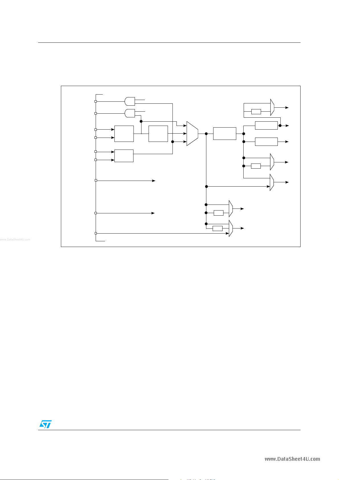
Figure 1. STR91xFA block diagram
1.8V
GND
3.0 or 3.3V
GND
VBATT
4 MHz to 2
MHz XTAL
EMI Ctrl
USB Bus
To Ethernet
PHY (MII) **
5
16 GPIO
EMI bus*** or
Ethernet**
or 16 GPIO
STR91xA
STR91x
CORE SUPPLY, VDD
CORE GND, VSS
I/O SUPPLY, VDDQ
I/O GND, VSSQ
BACKUP
SUPPLY
RTC
16
64K or 96K
Byte
SRAM
Arbiter
Data TCM
Interface
Control Logic / BIU and Write Buffer
Programmable Vectored
Programmable Vectored
Interrupt Controllers
Interrupt Controller
PLL, Power Management,
and Supervisory Reset
External Memory
Interface (EMI)***,
Muxed Address/Data
Programmable DMA
Controller (8 ch.)
USB* Full Speed, 10
Endpoints with FIFOs
Ethernet**
MAC, 10/100
Stacked Burst Flash Memory Die
Main Flash 256K,
or 512K Bytes
ARM966E-S
RISC CPU Core
AMBA / AHBA Interface
AHB
AHB
APB
Request
from
UART,
I2C,
SPI,
Timers,
Ext Re
Dedicated
DMA
ADC
JTAG ISP
Burst Interface
Burst Interface
Pre-Fetch Que
and Branch
Cache
Instruction
TCM
Interface
APB
to
32
q
2nd Flash
32K Bytes
JTAG
Debug
and
ETM
Real Time Clock
Wake Up
(4) 16-bit Timers,
CAPCOM, PWM
Motor Control,
3-ph Induction
(3) UART w/ IrDA
(2) I2C
(80) GPIO****
(2) SPI
CAN 2.0B
8 Channel 10-bit
ADC
Watchdog Tmr
ETM
JTAG
32.768 kHz
XTAL
48
MUX to 48 GPIO
AVDD
AVREF*
AVSS
* USB not available on STR910
** Ethernet MAC not available on STR910 and STR911
*** EMI not available on LQFP80
**** Only 40 GPIOs on LQFP80
9/78

www.DataSheet4U.com
Functional overview STR91xFA
2.5 SRAM (64K or 96K Bytes)
A 32-bit wide SRAM resides on the CPU’s Data TCM (D-TCM) interface, providing single-cycle
data accesses. As shown in Figure 1, the D-TCM shares SRAM access with the Advanced
High-performance Bus (AHB). Sharing is controlled by simple arbitration logic to allow the DMA
unit on the AHB to also access to the SRAM.
2.5.1 Arbitration
Zero-wait state access occurs for either the D-TCM or the AHB when only one of the two is
requesting SRAM. When both request SRAM simultaneously, access is granted on an
interleaved basis so neither requestor is starved, granting one 32-bit word transfer to each
requestor before relinquishing SRAM to the other. When neither the D-TCM or the AHB are
requesting SRAM, the arbiter leaves access granted to the most recent user (if D-TCM was last
to use SRAM then the D-TCM will not have to arbitrate to get access next time).
The CPU may execute code from SRAM through the AHB. There are no wait states as long as
the D-TCM is not contending for SRAM access and the AHB is not sharing bandwidth with
peripheral traffic. The ARM966E-S CPU core has a small pre-fetch queue built into this
instruction path through the AHB to look ahead and fetch instructions during idle bus cycles.
2.5.2 Battery backup
When a battery is connected to the designated battery backup pin (VBATT), SRAM contents
are automatically preserved when the normal operating voltage on VDD pins is lost or sags
below threshold. Automatic switchover to SRAM can be disabled by firmware if it is desired that
the battery will power only the RTC and not the SRAM during standby.
2.6 DMA data movement
DMA channels on the Advanced High-performance Bus (AHB) take full advantage of the
separate data path provided by the Harvard architecture, moving data rapidly and largely
independent of the instruction path. There are two DMA units, one is dedicated to move data
between the Ethernet interface and SRAM, the other DMA unit has eight programmable
channels with 16 request signals to service other peripherals and interfaces (USB, SSP, I2C,
ADC, UART, Timers, EMI, and external request pins). Both single word and burst DMA transfers
are supported. Memory-to-memory transfers are supported in addition to memory-peripheral
transfers. DMA access to SRAM is shared with D-TCM accesses, and arbitration is described
in Section 2.5.1. Efficient DMA transfers are managed by firmware using linked list descriptor
tables. Of the 16 DMA request signals, two are assigned to external inputs. The DMA unit can
move data between external devices and resources inside the STR91xFA through the EMI bus.
2.7 Non-volatile memories
There are two independent 32-bit wide Burst Flash memories enabling true read-while-write
operation. The Flash memories are single-voltage erase/program with 20 year minimum data
retention and 100K minimum erase cycles. The primary Flash memory is much larger than the
secondary Flash.
Both Flash memories are blank when devices are shipped from ST. The CPU can boot only
from Flash memory (configurable selection of which Flash bank).
10/78

www.DataSheet4U.com
STR91xFA Functional overview
Flash memories are programmed half-word (16 bits) at a time, but are erased by sector or by
full array.
2.7.1 Primary Flash memory
Using the STR91xFA device configuration software tool and 3rd party Integrated Developer
Environments, it is possible to specify that the primary Flash memory is the default memory
from which the CPU boots at reset, or otherwise specify that the secondary Flash memory is
the default boot memory. This choice of boot memory is non-volatile and stored in a location
that can be programmed and changed only by JTAG In-System Programming. See Section 5:
Memory mapping, for more detail.
The primary Flash memory has equal length 64K byte sectors. Devices with 256 Kbytes of
primary Flash have four sectors and 512K devices have eight sectors.
2.7.2 Secondary Flash memory
The smaller of the two Flash memories can be used to implement a bootloader, capable of
storing code to perform robust In-Application Programming (IAP) of the primary Flash memory.
The CPU executes code from the secondary Flash, while updating code in the primary Flash
memory. New code for the primary Flash memory can be downloaded over any of the
interfaces on the STR91xFA (USB, Ethernet, CAN, UART, etc.)
Additionally, the Secondary Flash memory may also be used to store small data sets by
emulating EEPROM though firmware, eliminating the need for external EEPROM memories.
This raises the data security level because passcodes and other sensitive information can be
securely locked inside the STR91xFA device.
The secondary Flash memory is 32 Kbytes and has four equal length sectors of 8 Kbytes each.
Both the primary Flash memory and the secondary Flash memory can be programmed with
code and/or data using the JTAG In-System Programming (ISP) channel, totally independent of
the CPU. This is excellent for iterative code development and for manufacturing.
2.8 One-time-programmable (OTP) memory
There are 32 bytes of OTP memory ideally suited for serial numbers, security keys, factory
calibration constants, or other permanent data constants. These OTP data bytes can be
programmed only one time through either the JTAG interface or by the CPU, and these bytes
can never be altered afterwards. As an option, a “lock bit” can be set by the JTAG interface or
the CPU which will block any further writing to the this OTP area. The “lock bit” itself is also
OTP. If the OTP array is unlocked, it is always possible to go back and write to an OTP byte
location that has not been previously written, but it is never possible to change an OTP byte
location if any one bit of that particular byte has been written before. The last two OTP bytes are
reserved for the STR91xFA product ID and revision level.
2.8.1 Product ID and revision level
OTP bytes 31 and 30 are programmed at ST factory before shipment and may be read by
firmware to determine the STR91xFA product type and silicon revision so it can optionally take
action based on the silicon on which it is running. Byte 31 contains the the major family
identifier of "9" (for STR9) in the high-nibble location, and the minor family identifier in the lownibble location. Today the low-nibble contains "1", but future family members may have other
11/78
www.DataSheet4U.com
Functional overview STR91xFA
values indicating memory size or other differentiating features. Byte 30 contains the silicon
revision level indicator. See Ta bl e 2 for values related to the two revisions of STR9 production
devices. See the Errata Sheet documents for STR91xF and STR91xFA for details of external
identification of silicon revisions.
Table 2. Product ID and revision level values
Production salestype Silicon revision OTP byte 31 OTP byte 30
STR91xFxxxxx Rev D 91h 03h
STR91xFAxxxxx Rev G 91h 20h
2.9 Vectored interrupt controller (VIC)
Interrupt management in the STR91xFA is implemented from daisy-chaining two standard ARM
VIC units. This combined VIC has 32 prioritized interrupt request channels and generates two
interrupt output signals to the CPU. The output signals are FIQ and IRQ, with FIQ having higher
priority.
2.9.1 FIQ handling
FIQ (Fast Interrupt reQuest) is the only non-vectored interrupt and the CPU can execute an
Interrupt Service Routine (ISR) directly without having to determine/prioritize the interrupt
source, minimizing ISR latency. Typically only one interrupt source is assigned to FIQ. An FIQ
interrupt has its own set of banked registers to minimize the time to make a context switch. Any
of the 32 interrupt request input signals coming into the VIC can be assigned to FIQ.
2.9.2 IRQ handling
IRQ is a vectored interrupt and is the logical OR of all 32 interrupt request signals coming into
the 32 IRQ channels. Priority of individual vectored interrupt requests is determined by
hardware (IRQ channel Intr 0 is highest priority, IRQ channel Intr 31 is lowest).
However, inside the same VIC (primary or secondary VIC), CPU firmware may re-assign
individual interrupt sources to individual hardware IRQ channels, meaning that firmware can
effectively change interrupt priority levels as needed within the same VIC (from priority 0 to
priority 16).
Note: Note: VIC0 (primary VIC) interrupts always have higher priority than VIC1 (secondary VIC)
interrupts
When the IRQ signal is activated by an interrupt request, VIC hardware will resolve the IRQ
interrupt priority, then the ISR reads the VIC to determine both the interrupt source and the
vector address to jump to the service code.
The STR91xFA has a feature to reduce ISR response time for IRQ interrupts. Typically, it
requires two memory accesses to read the interrupt vector address from the VIC, but the
STR91xFA reduces this to a single access by adding a 16th entry in the instruction branch
cache, dedicated for interrupts. This 16th cache entry always holds the instruction that reads
the interrupt vector address from the VIC, eliminating one of the memory accesses typically
required in traditional ARM implementations.
12/78
www.DataSheet4U.com
STR91xFA Functional overview
2.9.3 Interrupt sources
The 32 interrupt request signals coming into the VIC on 32 IRQ channels are from various
sources; 5 from a wake-up unit and the remaining 27 come from internal sources on the
STR91xFA such as on-chip peripherals, see Ta b le 3 . Optionally, firmware may force an
interrupt on any IRQ channel.
One of the 5 interrupt requests generated by the wake-up unit (IRQ25 in Ta b le 3 ) is derived
from the logical OR of all 32 inputs to the wake-up unit. Any of these 32 inputs may be used to
wake up the CPU and cause an interrupt. These 32 inputs consist of 30 external interrupts on
selected and enabled GPIO pins, plus the RTC interrupt, and the USB Resume interrupt.
Each of 4 remaining interrupt requests generated by the wake-up unit (IRQ26 in Ta bl e 3 ) are
derived from groupings of 8 interrupt sources. One group is from GPIO pins P3.2 to P3.7 plus
the RTC interrupt and the USB Resume interrupt; the next group is from pins P5.0 to P5.7; the
next group is from pins P6.0 to P6.7; and last the group is from pins P7.0 to P7.7. This allows
individual pins to be assigned directly to vectored IRQ interrupts or one pin assigned directly to
the non-vectored FIQ interrupt.
Table 3. VIC IRQ Channels
IRQ Channel
hardware
priority
0 (high priority) VIC0.0 WatchDog Timeout in WDT mode, Terminal Count in Counter Mode
1 VIC0.1 CPU Firmware Firmware generated interrupt
2 VIC0.2 CPU Core Debug Receive Command
3 VIC0.3 CPU Core Debug Transmit Command
4 VIC0.4 TIM Timer 0 Logic OR of ICI0_0, ICI0_1, OCI0_0, OCI0_1, Timer overflow
5 VIC0.5 TIM Timer 1 Logic OR of ICI1_0, ICI1_1, OCI1_0, OCI1_1, Timer overflow
6 VIC0.6 TIM Timer 2 Logic OR of ICI2_0, ICI2_1, OCI2_0, OCI2_1, Timer overflow
7 VIC0.7 TIM Timer 3 Logic OR of ICI3_0, ICI3_1, OCI3_0, OCI3_1, Timer overflow
8 VIC0.8 USB Logic OR of high priority USB interrupts
9 VIC0.9 USB Logic OR of low priority USB interrupts
10 VIC0.10 CCU Logic OR of all interrupts from Clock Control Unit
11 VIC0.11 Ethernet MAC
12 VIC0.12 DMA
13 VIC0.13 CAN Logic OR of all CAN interface interrupt sources
14 VIC0.14 IMC Logic OR of 8 Induction Motor Control Unit interrupts
15 VIC0.15 ADC End of AtoD conversion interrupt
16 VIC1.0 UART0 Logic OR of 5 interrupts from UART channel 0
17 VIC1.1 UART1 Logic OR of 5 interrupts from UART channel 1
18 VIC1.2 UART2 Logic OR of 5 interrupts from UART channel 2
19 VIC1.3 I2C0
20 VIC1.4 I2C1
21 VIC1.5 SSP0 Logic OR of all interrupts from SSP channel 0
22 VIC1.6 SSP1 Logic OR of all interrupts from SSP channel 1
23 VIC1.7 BROWNOUT LVD warning interrupt
24 VIC1.8 RTC Logic OR of Alarm, Tamper, or Periodic Timer interrupts
VIC input
channel
Logic Block Interrupt Source
Logic OR of Ethernet MAC interrupts via its own dedicated
DMA channel.
Logic OR of interrupts from each of the 8 individual DMA
channels
Logic OR of transmit, receive, and error interrupts of I2C
channel 0
Logic OR of transmit, receive, and error interrupts of I2C
channel 1
13/78
www.DataSheet4U.com
Functional overview STR91xFA
Table 3. VIC IRQ Channels
IRQ Channel
hardware
priority
25 VIC1.9 Wake-Up (all)
26 VIC1.10 Wake-up Group 0
27 VIC1.11 Wake-up Group 1 Logic OR of 8 interrupts from pins P5.0 to P5.7
28 VIC1.12 Wake-up Group 2 Logic OR of 8 interrupts from pins P6.0 to P6.7
29 VIC1.13 Wake-up Group 3 Logic OR of 8 interrupts from pins P7.0 to P7.7
30 VIC1.14 USB USB Bus Resume Wake-up (also input to wake-up unit)
31 (low priority) VIC1.15 PFQ-BC
VIC input
channel
Logic Block Interrupt Source
Logic OR of all 32 inputs of Wake-Up unit (30 pins, RTC, and
USB Resume)
Logic OR of 8 interrupt sources: RTC, USB Resume, pins
P3.2 to P3.7
Special use of interrupts from Prefetch Queue and Branch
Cache
2.10 Clock control unit (CCU)
The CCU generates a master clock of frequency f
generates individually scaled and gated clock sources to each of the following functional blocks
within the STR91xFA.
● CPU, f
●
●
●
●
●
●
CPUCLK
Advanced High-performance Bus (AHB), f
Advanced Peripheral Bus (APB), f
Flash Memory Interface (FMI), f
External Memory Interface (EMI), f
UART Baud Rate Generators, f
USB, f
USB
2.10.1 Master clock sources
The master clock in the CCU (f
firmware control, the CPU can switch between the three CCU inputs without introducing any
glitches on the master clock output. Inputs to the CCU are:
● Main Oscillator (f
crystal connected to STR91xFA pins X1_CPU and X2_CPU, or an external oscillator
device connected to pin X1_CPU.
● PLL (f
). The PLL takes the 4 to 25 MHz oscillator clock as input and generates a master
PLL
clock output up to 96 MHz (programmable). By default, at power-up the master clock is
sourced from the main oscillator until the PLL is ready (locked) and then the CPU may
switch to the PLL source under firmware control. The CPU can switch back to the main
oscillator source at any time and turn off the PLL for low-power operation. The PLL is
always turned off in Sleep mode.
● RTC (f
RTC
X2_RTC, or an external oscillator connected to pin X1_RTC to constantly run the real-time
clock unit. This 32.768 kHz clock source can also be used as an input to the CCU to run
the CPU in slow clock mode for reduced power.
OSC
). A 32.768 kHz external crystal can be connected to pins X1_RTC and
. From this master clock the CCU also
MSTR
HCLK
PCLK
FMICLK
BCLK
BAUD
) is derived from one of three clock input sources. Under
MSTR
). The source for the main oscillator input is a 4 to 25 MHz external
14/78
www.DataSheet4U.com
STR91xFA Functional overview
As an option, there are a number of peripherals that do not have to receive a clock sourced
from the CCU. The USB interface can receive an external clock on pin P2.7, TIM timers TIM0/
TIM1 can receive an external clock on pin P2.4, and timers TIM2/TIM3 on pin P2.5.
Figure 2. Clock control
JRTCLK
MII_PHYCLK
X1_CPU
X1_CPU
X1_RTC
X2_RTC
EXTCLK_T0T1
EXTCLK_T2T3
USB_CLK48M
32.768 kHz
25MHz
4-25MHz
48MHz
Main
OSC
RTC
OSC
Timer 0 & 1
External clock
Timer 2 & 3
External clock
2.10.2 Reference clock (RCLK)
RTCSEL
f
OSC
32.768 kHz
f
RTC
PHYSEL
PLL
f
PLL
Master CLK
f
MSTR
(1,2,4,8,16,1024)
1/2
1/2
RCLK
DIV
RCLK
BRCLK
To UA RT
USBCLK
To US B
1/2
AHB DIV
(1,2,4)
APB DIV)
(1,2,4,8)
1/2
EMI_BCLK
HCLK
PCLK
FMICLK
CPUCLK
The main clock (f
) can be divided to operate at a slower frequency reference clock (RCLK)
MSTR
for the ARM core and all the peripherals. The RCLK provides the divided clock for the ARM
core, and feeds the dividers for the AHB, APB, External Memory Interface, and FMI units.
2.10.3 AHB clock (HCLK)
The RCLK can be divided by 1, 2 or 4 to generate the AHB clock. The AHB clock is the bus
clock for the AHB bus and all bus transfers are synchronized to this clock. The maximum HCLK
frequency is 96 MHz.
2.10.4 APB clock (PCLK)
The RCLK can be divided by 1, 2, 4 or 8 to generate the APB clock. The APB clock is the bus
clock for the APB bus and all bus transfers are synchronized to this clock. Many of the
peripherals that are connected to the AHB bus also use the PCLK as the source for external
bus data transfers. The maximum PCLK frequency is 48 MHz.
2.10.5 Flash memory interface clock (FMICLK)
The FMICLK clock is an internal clock derived from RCLK, defaulting to RCLK frequency at
power up. The clock can be optionally divided by 2. The FMICLK determines the bus bandwidth
15/78

www.DataSheet4U.com
Functional overview STR91xFA
between the ARM core and the Flash memory. Typically, codes in the Flash memory can be
fetched one word per FMICLK clock in burst mode. The maximum FMICLK frequency is
96MHz.
2.10.6 Baud rate clock (BRCLK)
The baud rate clock is an internal clock derived from f
MSTR
UART peripherals for baudrate generation. The frequency can be optionally divided by 2.
2.10.7 External memory interface bus clock (BCLK)
The BCLK is an internal clock that controls the EMI bus. All EMI bus signals are synchronized
to the BCLK. The BCLK is derived from the HCLK and the frequency can be configured to be
the same or half that of the HCLK. Refer to Table 12 on page 53 for the maximum BCLK
frequency (f
). The BCLK clock is available on the LFBGA package as an output pin.
BCLK
2.10.8 USB interface clock
Special consideration regarding the USB interface: The clock to the USB interface must operate
at 48 MHz and comes from one of three sources, selected under firmware control:
● CCU master clock output of 48 MHz.
● CCU master clock output of 96 MHz. An optional divided-by-two circuit is available to
produce 48 MHz for the USB while the CPU system runs at 96MHz.
● STR91xFA pin P2.7. An external 48 MHz oscillator connected to pin P2.7 can directly
source the USB while the CCU master clock can run at some frequency other than 48 or
96 MHz.
2.10.9 Ethernet MAC clock
Special consideration regarding the Ethernet MAC: The external Ethernet PHY interface device
requires it’s own 25 MHz clock source. This clock can come from one of two sources:
● A 25 MHz clock signal coming from a dedicated output pin (P5.2) of the STR91xFA. In this
case, the STR91xFA must use a 25 MHz signal on its main oscillator input in order to pass
this 25 MHz clock back out to the PHY device through pin P5.2. The advantage here is that
an inexpensive 25 MHz crystal may be used to source a clock to both the STR91xFA and
the external PHY device.
● An external 25 MHz oscillator connected directly to the external PHY interface device. In
this case, the STR91xFA can operate independent of 25 MHz.
that is used by the three on-chip
2.10.10 External RTC calibration clock
The RTC_CLK can be enabled as an output on the JRTCK pin. The RTC_CLK is used for RTC
oscillator calibration. The RTC_CLK is active in Sleep mode and can be used as a system wake
up control clock.
2.10.11 Operation example
As an example of CCU operation, a 25 MHz crystal can be connected to the main oscillator
input on pins X1_CPU and X2_CPU, a 32.768 kHz crystal connected to pins X1_RTC and
X2_RTC, and the clock input of an external Ethernet PHY device is connected to STR91xFA
output pin P5.2. In this case, the CCU can run the CPU at 96 MHz from PLL, the USB interface
16/78

www.DataSheet4U.com
STR91xFA Functional overview
at 48 MHz, and the Ethernet interface at 25 MHz. The RTC is always running in the background
at 32.768 kHz, and the CPU can go to very low power mode dynamically by running from
32.768 kHz and shutting off peripheral clocks and the PLL as needed.
2.11 Flexible power management
The STR91xFA offers configurable and flexible power management control that allows the user
to choose the best power option to fit the application. Power consumption can be dynamically
managed by firmware and hardware to match the system’s requirements. Power management
is provided via clock control to the CPU and individual peripherals.
Clocks to the CPU and peripherals can be individually divided and gated off as needed. In
addition to individual clock divisors, the CCU master clock source going to the CPU, AHB, APB,
EMI, and FMI can be divided dynamically by as much as 1024 for low power operation.
Additionally, the CCU may switch its input to the 32.768 kHz RTC clock at any time for low
power.
The STR91xFA supports the following three global power control modes:
● Run Mode: All clocks are on with option to gate individual clocks off via clock mask
registers.
● Idle Mode: CPU and FMI clocks are off until an interrupt, reset, or wake-up occurs. Pre-
configured clock mask registers selectively allow individual peripheral clocks to continue
run during Idle Mode.
● Sleep Mode: All clocks off except RTC clock. Wake up unit remains powered, PLL is
forced off.
A special mode is used when JTAG debug is active which never gates off any clocks even if the
CPU enters Idle or Sleep mode.
2.11.1 Run mode
This is the default mode after any reset occurs. Firmware can gate off or scale any individual
clock. Also available is a special Interrupt Mode which allows the CPU to automatically run full
speed during an interrupt service and return back to the selected CPU clock divisor rate when
the interrupt has been serviced. The advantage here is that the CPU can run at a very low
frequency to conserve power until a periodic wake-up event or an asynchronous interrupt
occurs at which time the CPU runs full speed immediately.
2.11.2 Idle mode
In this mode the CPU suspends code execution and the CPU and FMI clocks are turned off
immediately after firmware sets the Idle Bit. Various peripherals continue to run based on the
settings of the mask registers that exist just prior to entering Idle Mode. There are 3 ways to exit
Idle Mode and return to Run Mode:
● Any reset (external reset pin, watchdog, low-voltage, power-up, JTAG debug command)
● Any interrupt (external, internal peripheral, RTC alarm or interval)
● Input from wake-up unit on GPIO pins
Note: It is possible to remain in Idle Mode for the majority of the time and the RTC can be
programmed to periodically wake up to perform a brief task or check status.
17/78

www.DataSheet4U.com
Functional overview STR91xFA
2.11.3 Sleep mode
In this mode all clock circuits except the RTC are turned off and main oscillator input pins
X1_CPU and X2_CPU are disabled. The RTC clock is required for the CPU to exit Sleep Mode.
The entire chip is quiescent (except for RTC and wake-up circuitry). There are three means to
exit Sleep Mode and re-start the system:
● Some resets (external reset pin, low-voltage, power-up, JTAG debug command)
● RTC alarm
● Input from wake-up unit
2.12 Voltage supplies
The STR91xFA requires two separate operating voltage supplies. The CPU and memories
operate from a 1.65V to 2.0V on the VDD pins, and the I/O ring operates at 2.7V to 3.6V on the
VDDQ pins.
2.12.1 Independent A/D converter supply and reference voltage
The ADC unit on 128-pin and 144-ball packages has an isolated analog voltage supply input at
pin AVDD to accept a very clean voltage source, independent of the digital voltage supplies.
Additionally, an isolated analog supply ground connection is provided on pin AVSS only on 128pin and 144-ball packages for further ADC supply isolation. On 80-pin packages, the analog
voltage supply is shared with the ADC reference voltage pin (as described next), and the
analog ground is shared with the digital ground at a single point in the STR91xFA device on pin
AVSS_VSSQ.
A separate external analog reference voltage input for the ADC unit is available on 128-pin and
144-ball packages at the AVREF pin for better accuracy on low voltage inputs. For 80-pin
packages, the ADC reference voltage is tied internally to the ADC unit supply voltage at pin
AVREF_AVDD, meaning the ADC reference voltage is fixed to the ADC unit supply voltage.
See Table 7: Operating conditions, for restrictions to the relative voltage levels of VDDQ, AVDD,
AVREF, and AVREF_AVDD.
2.12.2 Battery supply
An optional stand-by voltage from a battery or other source may be connected to pin VBATT to
retain the contents of SRAM in the event of a loss of the V
automatically switch its supply from the internal V
of V
drops below that of VBATT.
DD
The VBATT pin also supplies power to the RTC unit, allowing the RTC to function even when
the main digital supplies (V
possible to select whether or not to power from VBATT only the RTC unit, or power the RTC unit
and the SRAM when the STR91xFA device is powered off.
DD
and V
supply. The SRAM will
DD
source to the VBATT pin when the voltage
DD
) are switched off. By configuring the RTC register, it is
DDQ
18/78

www.DataSheet4U.com
STR91xFA Functional overview
2.13 System supervisor
The STR91xFA monitors several system and environmental inputs and will generate a global
reset, a system reset, or an interrupt based on the nature of the input and configurable settings.
A global reset clears all functions on the STR91xFA, a system reset will clear all but the Clock
Control Unit (CCU) settings and the system status register. At any time, firmware may reset
individual on-chip peripherals. System supervisor inputs include:
● GR: CPU voltage supply (V
● GR: I/O voltage supply (V
● GR: Power-Up condition
● SR: Watchdog timer timeout
● SR: External reset pin (RESET_INn)
● SR: JTAG debug reset command
Note: GR: means the input causes Global Reset, SR: means the input causes System Reset
The CPU may read a status register after a reset event to determine if the reset was caused by
a watchdog timer timeout or a voltage supply drop out. This status register is cleared only by a
power up reset.
2.13.1 Supply voltage brownout
) drop out or brown out
DD
) drop out or brown out
DDQ
Each operating voltage source (VDD and V
Detect (LVD) circuitry. The LVD will generate an early warning interrupt to the CPU when
voltage sags on either V
DD
or V
applications because the system can perform an orderly shutdown before the batteries become
too weak. The voltage trip point to cause a brown out interrupt is typically 0.25V above the LVD
dropout thresholds that cause a reset.
CPU firmware may prevent all brown-out interrupts by writing to interrupt mask registers at runtime.
2.13.2 Supply voltage dropout
LVD circuitry will always cause a global reset if the CPU’s VDD source drops below it’s fixed
threshold of 1.4V.
However, the LVD trigger threshold to cause a global reset for the I/O ring’s V
to one of two different levels, depending if V
3.0V to 3.6V. If V
V
operation is 3.0V and 3.6V, the LVD threshold is 2.7V. The choice of trigger level is made
DDQ
by STR91xFA device configuration software from STMicroelectronics or IDE from 3rd parties,
and is programmed into the STR91xFA device along with other configurable items through the
JTAG interface when the Flash memory is programmed.
CPU firmware may prevent some LVD resets if desired by writing a control register at run-time.
Firmware may also disable the LVD completely for lowest-power operation when an external
LVD device is being used.
operation is at 2.7V to 3.3V, the LVD dropout trigger threshold is 2.4V. If
DDQ
) is monitored separately by the Low Voltage
DDQ
voltage inputs. This is an advantage for battery powered
DDQ
source is set
will be operated in the range of 2.7V to 3.3V, or
DDQ
DDQ
2.13.3 Watchdog timer
The STR91xFA has a 16-bit down-counter (not one of the four TIM timers) that can be used as
a watchdog timer or as a general purpose free-running timer/counter. The clock source is the
19/78

www.DataSheet4U.com
Functional overview STR91xFA
peripheral clock from the APB, and an 8-bit clock pre-scaler is available. When enabled by
firmware as a watchdog, this timer will cause a system reset if firmware fails to periodically
reload this timer before the terminal count of 0x0000 occurs, ensuring firmware sanity. The
watchdog function is off by default after a reset and must be enabled by firmware.
2.13.4 External RESET_INn pin
This input signal is active-low with hystereses (V
reset signals on the circuit board (such as closure to ground from a push-button) may be
connected directly to the RESET_INn pin, but an external pull-up resistor to V
present as there is no internal pullup on the RESET_INn pin.
A valid active-low input signal of t
reset within the STR91xFA. There is also a RESET_OUTn pin on the STR91xFA that can drive
other system components on the circuit board. RESET_OUTn is active-low and has the same
timing of the Power-On-Reset (POR) shown next, t
2.13.5 Power-up
The LVD circuitry will always generate a global reset when the STR91xFA powers up, meaning
internal reset is active until V
condition has a duration of t
0x0000.0000 in Flash memory. It is not possible for the CPU to boot from any other source
other than Flash memory.
2.13.6 JTAG debug command
When the STR91xFA is in JTAG debug mode, an external device which controls the JTAG
interface can command a system reset to the STR91xFA over the JTAG channel.
2.13.7 Tamper detection
). Other open-drain, active-low system
RHYS
must be
DDQ
duration on the RESET_INn pin will cause a system
RINMIN
.
POR
and VDD are both above the LVD thresholds. This POR
DDQ
, after which the CPU will fetch its first instruction from address
POR
On 128-pin and 144-ball STR91xFA devices only, there is a tamper detect input pin,
TAMPER_IN, used to detect and record the time of a tamper event on the end product such as
malicious opening of an enclosure, unwanted opening of a panel, etc. The activation mode of
the tamper pin is programmable to one of two modes. One is Normally Closed/Tamper Open,
the other mode will detect when a signal on the tamper input pin is driven from low-to-high, or
high-to-low depending on firmware configuration. Once a tamper event occurs, the RTC time
(millisecond resolution) and the date are recorded in the RTC unit. Simultaneously, the SRAM
standby voltage source will be cut off to invalidate all SRAM contents. Tamper detection control
and status logic are part of the RTC unit.
2.14 Real-time clock (RTC)
The RTC combines the functions of a complete time-of-day clock (millisecond resolution) with
an alarm programmable up to one month, a 9999-year calender with leap-year support,
periodic interrupt generation from 1 to 512 Hz, tamper detection (described in Section 2.13.7),
and an optional clock calibration output on the JRTCK pin. The time is in 24 hour mode, and
time/calendar values are stored in binary-coded decimal format.
The RTC also provides a self-isolation mode that is automatically activated during power down.
This feature allows the RTC to continue operation when V
20/78
and VDD are absent, as long as
DDQ

www.DataSheet4U.com
STR91xFA Functional overview
an alternate power source, such as a battery, is connected to the VBATT input pin. The current
drawn by the RTC unit on the VBATT pin is very low in this standby mode, I
RTC_STBY
.
2.15 JTAG interface
An IEEE-1149.1 JTAG interface on the STR91xFA provides In-System-Programming (ISP) of
all memory, boundary scan testing of pins, and the capability to debug the CPU.
STR91xFA devices are shipped from ST with blank Flash memories. The CPU can only boot
from Flash memory (selection of which Flash bank is programmable). Firmware must be initially
programmed through JTAG into one of these Flash memories before the STR91xFA is used.
Six pins are used on this JTAG serial interface. The five signals JTDI, JTDO, JTMS, JTCK, and
JTRSTn are all standard JTAG signals complying with the IEEE-1149.1 specification. The sixth
signal, JRTCK (Return TCK), is an output from the STR91xFA and it is used to pace the JTCK
clock signal coming in from the external JTAG test equipment for debugging. The frequency of
the JTCK clock signal coming from the JTAG test equipment must be at least 10 times less than
the ARM966E-S CPU core operating frequency (f
CPUCLK
output from the STR91xFA and is input to the external JTAG test equipment to hold off
transitions of JTCK until the CPU core is ready, meaning that the JTAG equipment cannot send
the next rising edge of JTCK until the equipment receives a rising edge of JRTCK from the
STR91xFA. The JTAG test equipment must be able to interpret the signal JRTCK and perform
this adaptive clocking function. If it is known that the CPU clock will always be at least ten times
faster than the incoming JTCK clock signal, then the JRTCK signal is not needed.
). To ensure this, the signal JRTCK is
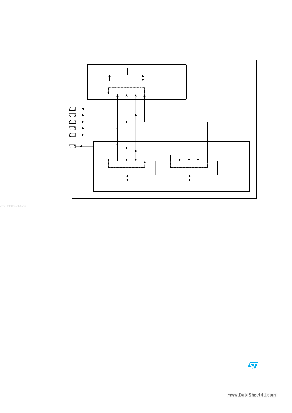
The two die inside the STR91xFA (CPU die and Flash memory die) are internally daisy-chained
on the JTAG bus, see Figure 3 on page 22. The CPU die has two JTAG Test Access Ports
(TAPs), one for boundary scan functions and one for ARM CPU debug. The Flash memory die
has one TAP for program/erase of non-volatile memory. Because these three TAPs are daisychained, only one TAP will converse on the JTAG bus at any given time while the other two
TAPs are in BYPASS mode. The TAP positioning order within this JTAG chain is the boundary
scan TAP first, followed by the ARM debug TAP, followed by the Flash TAP. All three TAP
controllers are reset simultaneously by one of two methods:
● A chip-level global reset, caused only by a Power-On-Reset (POR) or a Low Voltage
Detect (LVD).
● A reset command issued by the external JTAG test equipment. This can be the assertion
of the JTAG JTRSTn input pin on the STR91xFA or a JTAG reset command shifted into the
STR91xFA serially.
This means that chip-level system resets from watchdog time-out or the assertion of
RESET_INn pin do not affect the operation of any JTAG TAP controller. Only global resets
effect the TAPs.
21/78
www.DataSheet4U.com
Functional overview STR91xFA
Figure 3. JTAG chaining inside the STR91xFA
JTDO
JTRSTn
JTCK
JTMS
JTDI
JRTCK
MAIN FLASH SECONDARY FLASH
JTAG TAP CONTROLLER #3
TDO TMS TCK
TMS TCK TDO
TDI
JTAG TAP CONTROLLER #1
BOUNDARY SCAN
TRST
TDI
TRST
BURST FLASH
MEMORY DIE
JTAG
Instruction
regi ster length
is 8 bits
TDI
TRST
JTAG TAP CONTROLLER #2
CPU DEBUG
TCK
TMS
TDO
STR91xx
ARM966ES DIE
JTAG
Instruction
register length:
5 bits for TAP #1
4 bits for TAP #2
2.15.1 In-system-programming
The JTAG interface is used to program or erase all memory areas of the STR91xFA device. The
pin RESET_INn must be asserted during ISP to prevent the CPU from fetching invalid
instructions while the Flash memories are being programmed.
Note that the 32 bytes of OTP memory locations cannot be erased by any means once
programmed by JTAG ISP or the CPU.
2.15.2 Boundary scan
Standard JTAG boundary scan testing compliant with IEEE-1149.1 is available on the majority
of pins of the STR91xFA for circuit board test during manufacture of the end product.
STR91xFA pins that are not serviced by boundary scan are the following:
● JTAG pins JTCK, JTMS, JTDI, JTDO, JTRSTn, JRTCK
● Oscillator input pins X1_CPU, X2_CPU, X1_RTC, X2_RTC
● Tamper detect input pin TAMPER_IN (128-pin and 144-pin packages only)
2.15.3 CPU debug
The ARM966E-S CPU core has standard ARM EmbeddedICE-RT logic, allowing the
STR91xFA to be debugged through the JTAG interface. This provides advanced debugging
features making it easier to develop application firmware, operating systems, and the hardware
22/78

www.DataSheet4U.com
STR91xFA Functional overview
itself. Debugging requires that an external host computer, running debug software, is connected
to the STR91xFA target system via hardware which converts the stream of debug data and
commands from the host system’s protocol (USB, Ethernet, etc.) to the JTAG EmbeddedICERT protocol on the STR91xFA. These protocol converters are commercially available and
operate with debugging software tools.
The CPU may be forced into a Debug State by a breakpoint (code fetch), a watchpoint (data
access), or an external debug request over the JTAG channel, at which time the CPU core and
memory system are effectively stopped and isolated from the rest of the system. This is known
as Halt Mode and allows the internal state of the CPU core, memory, and peripherals to be
examined and manipulated. Typical debug functions are supported such as run, halt, and
single-step. The EmbeddedICE-RT logic supports two hardware compare units. Each can be
configured to be either a watchpoint or a breakpoint. Breakpoints can also be data-dependent.
Debugging (with some limitations) may also occur through the JTAG interface while the CPU is
running full speed, known as Monitor Mode. In this case, a breakpoint or watchpoint will not
force a Debug State and halt the CPU, but instead will cause an exception which can be tracked
by the external host computer running monitor software. Data can be sent and received over
the JTAG channel without affecting normal instruction execution. Time critical code, such as
Interrupt Service Routines may be debugged real-time using Monitor Mode.
2.15.4 JTAG security bit
This is a non-volatile bit (Flash memory based), which when set will not allow the JTAG
debugger or JTAG programmer to read the Flash memory contents.
Using JTAG ISP, this bit is typically programmed during manufacture of the end product to
prevent unwanted future access to firmware intellectual property. The JTAG Security Bit can be
cleared only by a JTAG “Full Chip Erase” command, making the STR91xFA device blank and
ready for programming again. The CPU can read the status of the JTAG Security Bit, but it may
not change the bit value.
2.16 Embedded trace module (ARM ETM9, v. r2p2)
The ETM9 interface provides greater visibility of instruction and data flow happening inside the
CPU core by streaming compressed data at a very high rate from the STR91xFA though a
small number of ETM9 pins to an external Trace Port Analyzer (TPA) device. The TPA is
connected to a host computer using USB, Ethernet, or other high-speed channel. Real-time
instruction flow and data activity can be recorded and later formatted and displayed on the host
computer running debugger software, and this software is typically integrated with the debug
software used for EmbeddedICE-RT functions such as single-step, breakpoints, etc. Tracing
may be triggered and filtered by many sources, such as instruction address comparators, data
watchpoints, context ID comparators, and counters. State sequencing of up to three triggers is
also provided. TPA hardware is commercially available and operates with debugging software
tools.
The ETM9 interface is nine pins total, four of which are data lines, and all pins can be used for
GPIO after tracing is no longer needed. The ETM9 interface is used in conjunction with the
JTAG interface for trace configuration. When tracing begins, the ETM9 engine compresses the
data by various means before broadcasting data at high speed to the TPA over the four data
lines. The most common ETM9 compression technique is to only output address information
when the CPU branches to a location that cannot be inferred from the source code. This means
23/78

www.DataSheet4U.com
Functional overview STR91xFA
the host computer must have a static image of the code being executed for decompressing the
ETM9 data. Because of this, self-modified code cannot be traced.
2.17 Ethernet MAC interface with DMA
STR91xFA devices in 128-pin and 144-ball packages provide an IEEE-802.3-2002 compliant
Media Access Controller (MAC) for Ethernet LAN communications through an industry
standard Medium Independent Interface (MII). The STR91xFA requires an external Ethernet
physical interface device (PHY) to connect to the physical LAN bus (twisted-pair, fiber, etc.).
The PHY is connected to the STR91xFA MII port using as many as 18 signals (see pins which
have signal names MII_* in Ta bl e 5 ).
The MAC corresponds to the OSI Data Link layer and the PHY corresponds to the OSI Physical
layer. The STR91xFA MAC is responsible for:
● Data encapsulation, including frame assembly before transmission, and frame parsing/
error detection during and after reception.
● Media access control, including initiation of frame transmission and recover from
transmission failure.
The STR91xFA MAC includes the following features:
● Supports 10 and 100 Mbps rates
● Tagged MAC frame support (VLAN support)
● Half duplex (CSMA/CD) and full duplex operation
● MAC control sublayer (control frames) support
● 32-bit CRC generation and removal
● Several address filtering modes for physical and multicast address (multicast and group
addresses)
● 32-bit status code for each transmitted or received frame
● Internal FIFOs to buffer transmit and receive frames. Transmit FIFO depth is 4 words (32
bits each), and the receive FIFO is 16 words deep.
A 32-bit burst DMA channel residing on the AHB is dedicated to the Ethernet MAC for highspeed data transfers, side-stepping the CPU for minimal CPU impact during transfers. This
DMA channel includes the following features:
● Direct SRAM to MAC transfers of transmit frames with the related status, by descriptor
chain
● Direct MAC to SRAM transfers of receive frames with the related status, by descriptor
chain
● Open and Closed descriptor chain management
2.18 USB 2.0 slave device interface with DMA
The STR91xFA provides a USB slave controller that implements both the OSI Physical and
Data Link layers for direct bus connection by an external USB host on pins USBDP and
USBPN. The USB interface detects token packets, handles data transmission and reception,
and processes handshake packets as required by the USB 2.0 standard.
The USB slave interface includes the following features:
24/78