

Sony SSUS-501 Service manual
SS-US501/SW-US501/UZ-US501
This system incorporates Dolby* Digital and Pro Logic Surround and
the DTS** Digital Surround System.
* Manufactured under license from Dolby Laboratories.
Dolby , Pro Logic , and the double-D symbol are trademarks of
Dolby Laboratories.
**Manufactured under license from Digital Theater Systems, Inc. DTS and
DTS Digital Surround are registered trademarks of Digital Theater Systems, Inc.
SERVICE MANUAL
Ver 1.0 2004.01
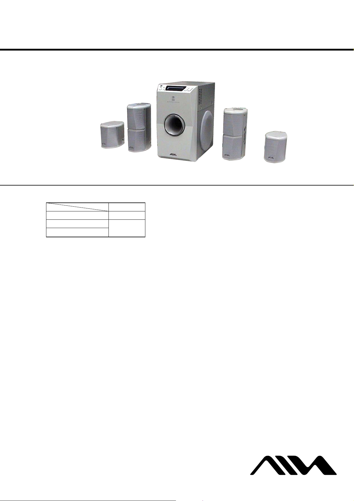
SS-US501
(SURROUND)
• UZ-US501 consists of the following models respectively.
Subwoofer SW-US501
Front/Center Speakers
Surround Speakers
SS-US501
(FRONT/CENTER)
UZ-US501
SS-US501
SW-US501
(SUBWOOFER)
SS-US501
(FRONT/CENTER)
US Model
AEP Model
UK Model
E Model
SS-US501
(SURROUND)
For the U.S.A. model
AUDIO POWER SPECIFICATIONS
POWER OUTPUT AND TOTAL
HARMONIC DISTORTION:
With 4 ohms loads subwoofer driven, from
20 - 200 Hz; rated 20 watts minimum RMS
power, with no more than 0.8% total
harmonic distortion from 250 milliwatts to
rated output.
SW-US501 (Subwoofer)
Max. output
Subwoofer: 30 W (4 ohms)
Front: 14 W + 14 W (8 ohms)
Dual center*: 14 W (4 ohms + 4 ohms)
Surround*: 14 W + 14 W (8 ohms)
* Depending on the sound field settings and the
source, there may be no sound output.
Speaker system Bass reflex type
Speaker unit 130 mm (5
Dimensions (approx.)
Mass (approx.) 5.8 kg (12 lb 13 oz)
SS-US501 (Front/Center speakers)
Speaker system Front: Closed box type
cone type
160 × 300 × 300 mm
(6
(w/h/d, not including the
projecting parts)
Center: Uni directional type
1
/8 in.) dia.
3
/8 × 11 7/8 × 11 7/8 in.)
SPECIFICATIONS
3
Speaker unit Front: 58 mm (2
Rated impedance
Dimensions (approx.)
Mass (approx.) 650g (1 lb 7 oz) × 2
Length of cable 3 m (9 ft.)
SS-US501 (Surround speakers)
Speaker system Closed box type
Speaker unit 58 mm (2
Rated impedance 8 ohms
Dimensions (approx.)
Mass (approx.) 350g (13 oz) × 2
Length of cable 8 m (24 ft.)
cone type
Center: 48 mm (1
cone type
Front: 8 ohms
Center: 4 ohms + 4 ohms
85 × 200 × 125 mm
3
(3
/8 × 7 7/8 × 5 in.)
(w/h/d, not including the
projecting parts)
3
85 × 106 × 125 mm
3
/8 × 4 1/4 × 5 in.)
(3
(w/h/d, not including the
projecting parts)
/8 in.) dia.
15
/16 in.) dia.
/8 in.) dia. cone type
USB ACTIVE SPEAKER SYSTEM
General
Power requirements
U.S.A. model: 120 V AC, 60 Hz
Other model: 220-240 V AC,
Power consumption
U.S.A. model: 75 W
Other model: 75 W
Operating temperature 5ßC to 35ßC
Operating humidity 5 % to 90 %
Supplied accessories
Design and specifications are subject to change
without notice.
50/60 Hz
1.2 W
(at the Power Saving Mode)
0.3 W
(at the Power Saving Mode)
USB cable 1.8 m
(5.9 ft.) (1)
Remote commander
(remote) RM-Z7S101 (1)
CD-ROM WinDVD (1)
Operating Instructions
(this book) (1)
9-877-530-01 Sony Corporation
2004A05-1 Aiwa Original Products
C 2004.01 Published by Sony Engineering Corporation
SS-US501/SW-US501/UZ-US501
r
Notes on chip component replacement
•Never reuse a disconnected chip component.
• Notice that the minus side of a tantalum capacitor may be damaged by heat.
SAFETY CHECK-OUT
After correcting the original service problem, perform the following safety check before releasing the set to the customer:
Check the antenna terminals, metal trim, “metallized” knobs,
screws, and all other exposed metal parts for AC leakage.
Check leakage as described below.
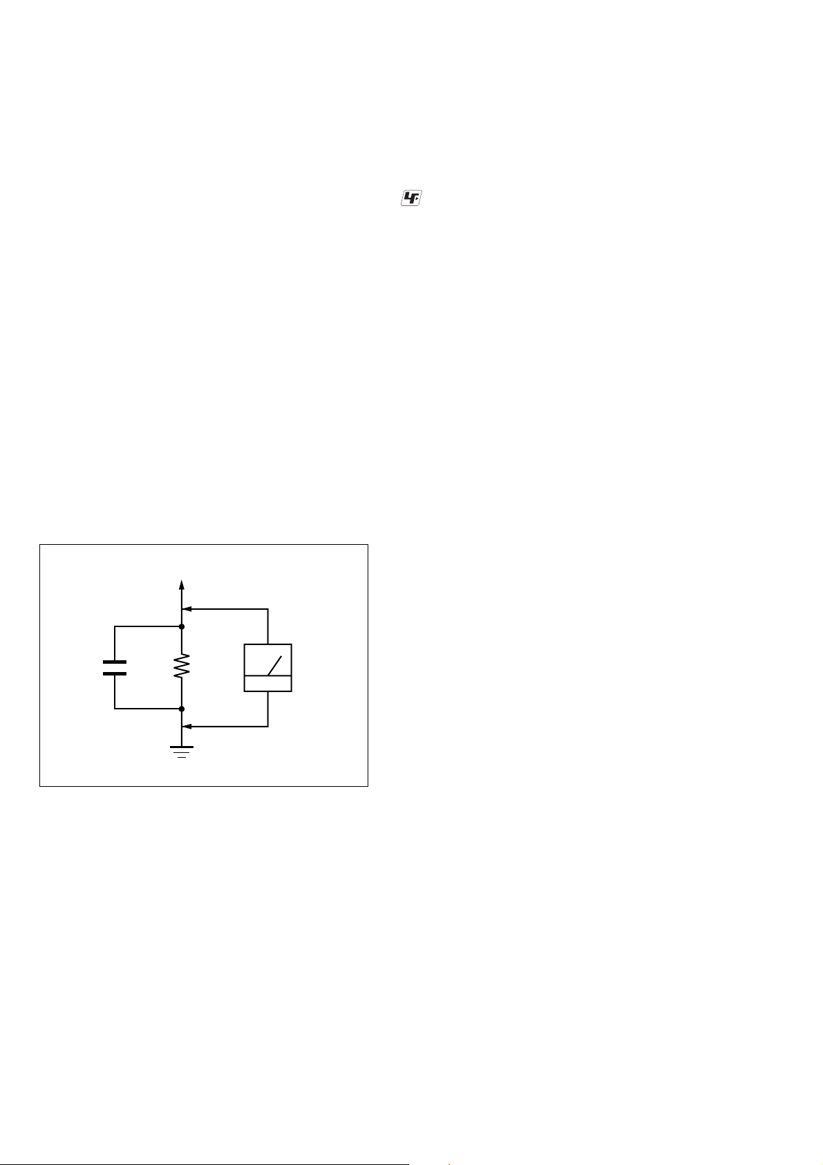
LEAKAGE TEST
The AC leakage from any exposed metal part to earth ground and
from all exposed metal parts to any exposed metal part having a
return to chassis, must not exceed 0.5 mA (500 microamperes.).
Leakage current can be measured by any one of three methods.
1. A commercial leakage tester, such as the Simpson 229 or RCA
WT -540A. Follo w the manufacturers’ instructions to use these
instruments.
2. A battery-operated AC milliammeter . The Data Precision 245
digital multimeter is suitable for this job.
3. Measuring the voltage drop across a resistor by means of a
VOM or battery-operated AC voltmeter. The “limit” indication is 0.75 V, so analog meters must have an accurate lowvoltage scale. The Simpson 250 and Sanwa SH-63Trd are e xamples of a passive VOM that is suitable. Nearly all battery
operated digital multimeters that have a 2 V A C range are suitable. (See Fig. A)
UNLEADED SOLDER
Boards requiring use of unleaded solder are printed with the leadfree mark (LF) indicating the solder contains no lead.
(Caution: Some printed circuit boards may not come printed with
the lead free mark due to their particular size)
: LEAD FREE MARK
Unleaded solder has the following characteristics.
• Unleaded solder melts at a temperature about 40 ˚C higher than
ordinary solder.
Ordinary soldering irons can be used but the iron tip has to be
applied to the solder joint for a slightly longer time.
Soldering irons using a temperature regulator should be set to
about 350 ˚C.
Caution: The printed pattern (copper foil) may peel away if the
heated tip is applied for too long, so be careful!
• Strong viscosity
Unleaded solder is more viscou-s (sticky, less prone to flow)
than ordinary solder so use caution not to let solder bridges occur such as on IC pins, etc.
• Usable with ordinary solder
It is best to use only unleaded solder but unleaded solder may
also be added to ordinary solder.
To Exposed Metal
Parts on Set
AC
1.5 k
0.15 µF
Fig. A. Using an AC voltmeter to check AC leakage.
Ω
Earth Ground
voltmete
(0.75 V)
SAFETY-RELATED COMPONENT WARNING!!
COMPONENTS IDENTIFIED BY MARK 0 OR DOTTED
LINE WITH MARK 0 ON THE SCHEMATIC DIAGRAMS
AND IN THE PARTS LIST ARE CRITICAL TO SAFE
OPERATION. REPLACE THESE COMPONENTS WITH
SONY PARTS WHOSE PART NUMBERS APPEAR AS
SHOWN IN THIS MANU AL OR IN SUPPLEMENTS PUBLISHED BY SONY.
2
SS-US501/SW-US501/UZ-US501
SECTION 1
SERVICING NOTE
TABLE OF CONTENTS
1. SERVICING NOTE................................................. 3
2. GENERAL .................................................................. 4
3. DISASSEMBLY
3-1. Disassembly Flow ........................................................... 6
3-2. Top Chassis ..................................................................... 6
3-3. DIGITAL Board .............................................................. 7
3-4. Front Cabinet Section ..................................................... 7
4. TEST MODE ............................................................. 8
5. DIAGRAMS
5-1. Block Diagram – MAIN Section –................................ 9
5-2. Block Diagram
– DISPLAY/POWER SUPPLY Section – ...................... 10
5-3. Note for Printed Wiring Boards and
Schematic Diagrams ....................................................... 11
5-4. Printed Wiring Board – DIGITAL Board –................... 12
5-4. Schematic Diagram – DIGITAL Board (1/5) – ............. 13
5-5. Schematic Diagram – DIGITAL Board (2/5) – ............. 14
5-6. Schematic Diagram – DIGITAL Board (3/5) – ............. 15
5-7. Schematic Diagram – DIGITAL Board (4/5) – ............. 16
5-9. Schematic Diagram – DIGITAL Board (5/5) – ............. 17
5-10. Printed Wiring Board – DISPLAY Board – .................. 18
5-11. Schematic Diagram – DISPLAY Board – ..................... 19
5-12. Printed Wiring Board – AMP Board – .......................... 20
5-13. Schematic Diagram – AMP Board – ............................. 21
5-14. Printed Wiring Board
– SUB Board (Except US model) –................................ 22
5-15. Schematic Diagram
– SUB Board (Except US model) –................................ 22
6. EXPLODED VIEWS
6-1. Overall Section................................................................ 33
6-2. Front Cabinet Section ..................................................... 34
6-3. Main Section ................................................................... 35
6-4. Rear Chassis Section....................................................... 36
6-5. Front/Surround Speaker Section..................................... 37
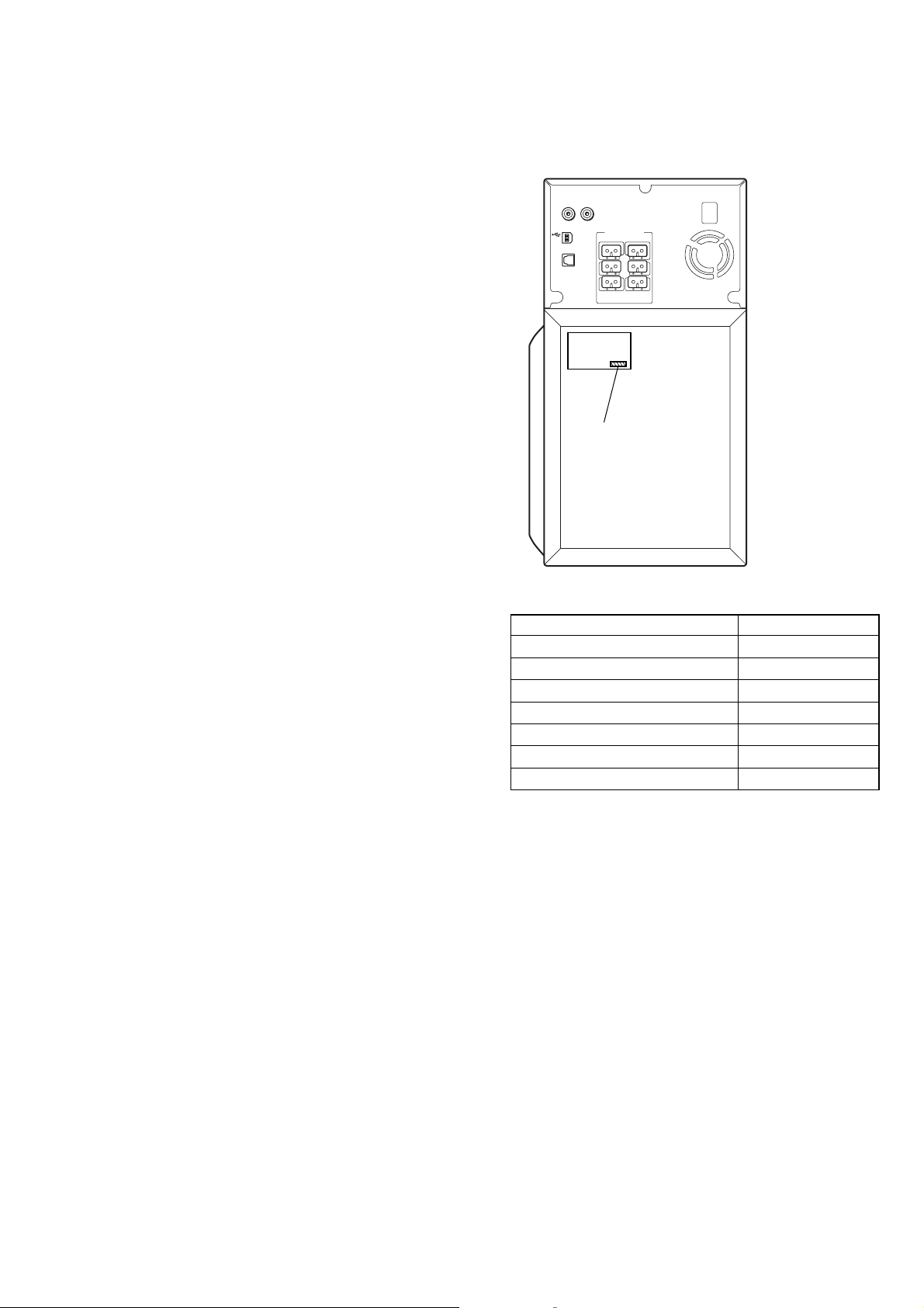
• MODEL IDENTIFICATION
– Rear View –
ANALOG IN
RL
SPEAKER
USB
OPTICAL IN
RL
FRONT
CENTER
SURROUND
PART No.
MODEL PART No.
UK model (WHITE) 4-254-202-0
Singapore model 4-254-615-0
Hong Kong model 4-254-915-0
AEP model (BLACK) 4-255-268-0
UK model (BLACK) 4-255-269-0
US model 4-255-394-0
AEP model (WHITE) 4-255-469-0
[]
[]
[]
[]
[]
[]
[]
7. ELECTRICAL PARTS LIST .............................. 38
3
SS-US501/SW-US501/UZ-US501
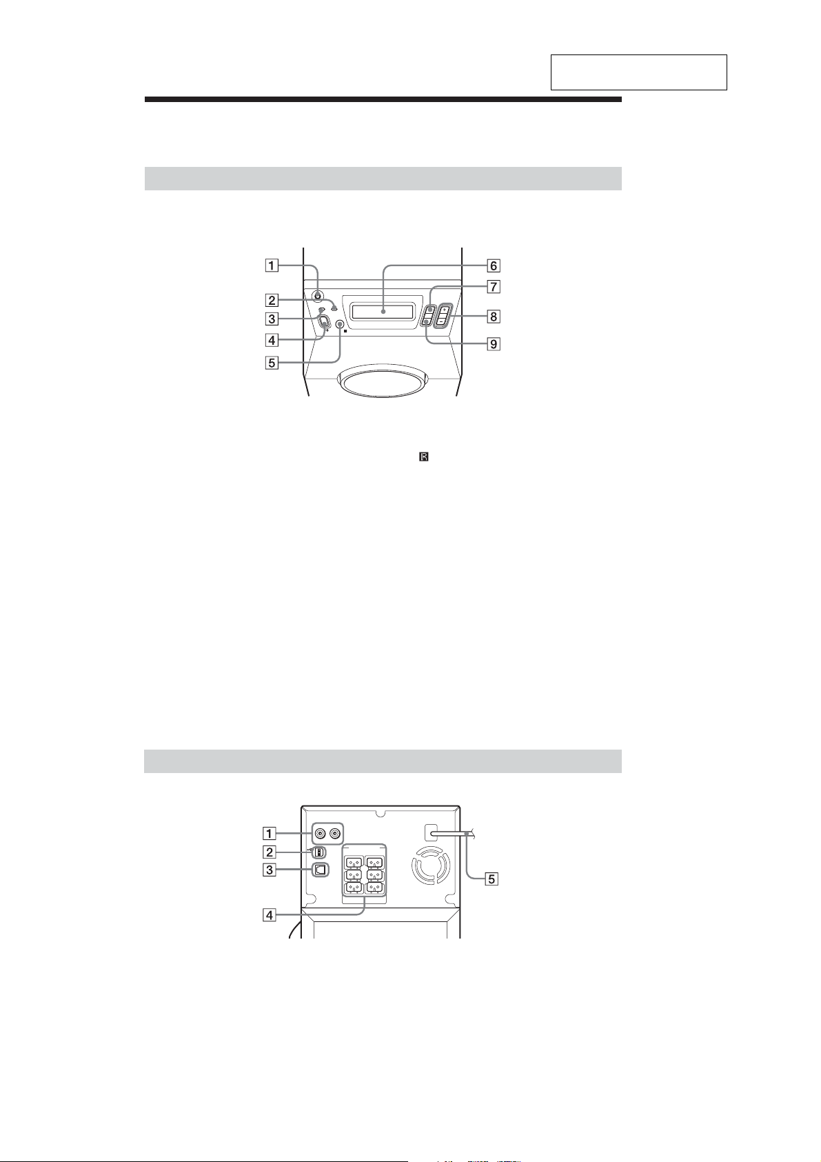
Index to Parts and Controls
Subwoofer (Front Panel)
SECTION 2
GENERAL
PHONES
AUTO POWER
S-MODE
This section is extracted from
instruction manual.
VOLUME
INPUT
1 HEADPHONE jack
Connect headphones here.
2 AUTO POWER indicator
When the system is in the AUTO
POWER ON mode, the indicator lights
up green.
3 ?/1 (POWER) indicator
When turned on, lights up green.
When turned off, lights up red (STANDBY MODE).
4 ?/1 (POWER)
Turns on and off the power of the
system.
Subwoofer (Rear Panel)
USB
OPTICAL IN
ANALOG IN
R
SURROUND
CENTER
L
FRONT
SPEAKER
R
5
Receives the remote control signals.
6 Display
Indicates the speaker setting, input
signal, sound field mode, etc.
7 INPUT
Select the input signal.
8 VOLUME +/−
Adjust the volume and select settings.
9 S-MODE
Adjust the sound field mode and select
settings.
L
(remote sensor)
1 ANALOG IN (L/R) jacks
Connect to the audio output of a TV,
VCR, etc.
2 USB jack
Connect to the computer.
3 OPTICAL IN jack
Connect to the DIGITAL OUT
(OPTICAL IN) jack of a DVD player,
etc.
4 SPEAKER jacks
Connect to the supplied satellite
speakers.
5 AC power cord (mains lead)
4
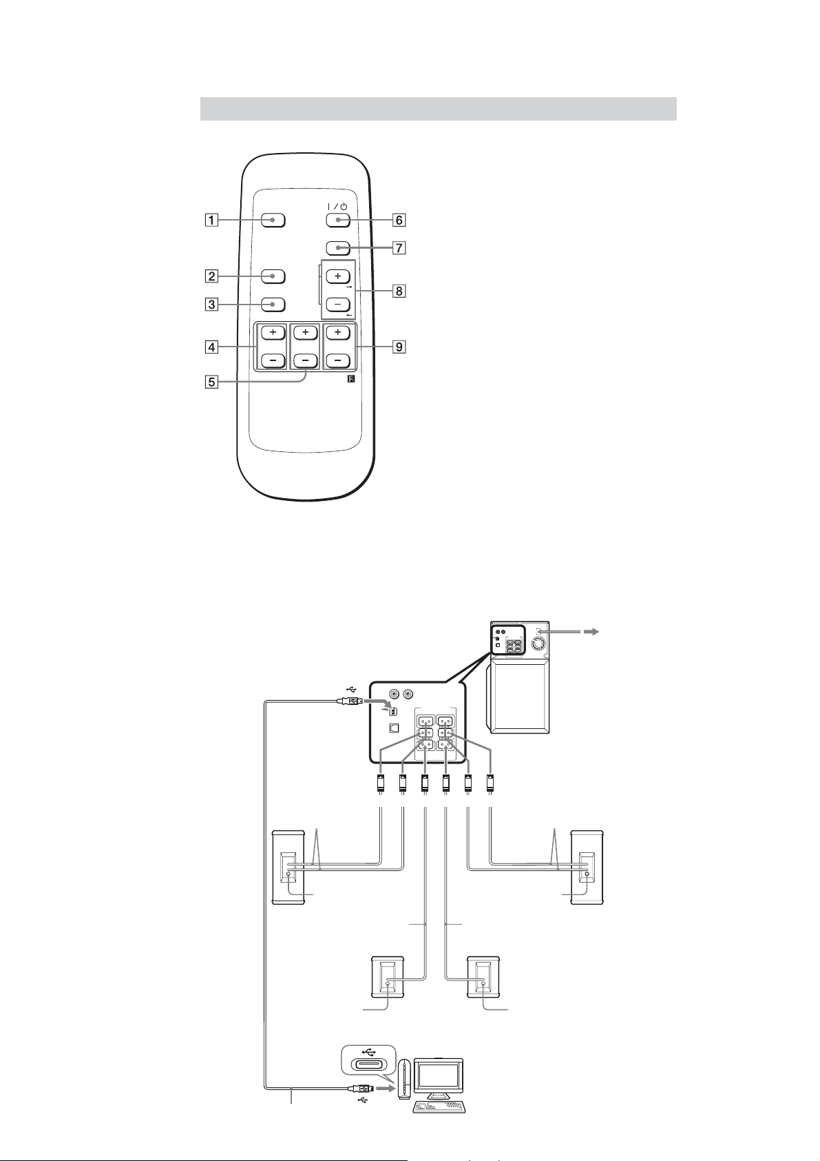
Remote
MUTING
TEST TONE
S-MODE
SET UP
SHIFT
SS-US501/SW-US501/UZ-US501
1 MUTING, TEST TONE
Mutes the sound.
Pressing this button while pressing
SHIFT will sound the test tone.
2 S-MODE, SET UP
INPUT
VOLUME
SELECT
SELECT
WOOFER
CENTERSURR
Selects the sound field mode.
Pressing this button while pressing
SHIFT will select the system menu.
3 SHIFT
Switches the function of the buttons on
the remote.
4 SURR +/−
Adjust the surround speakers volume.
5 CENTER +/−
Adjust the center speaker volume.
6 ?/1 (POWER)
Turns on and off the system.
7 INPUT
Selects the input signal.
8 VOLUME +/− , SELECT C/c
Makes the speaker settings or adjusts the
volume of the system.
Pressing this button while pressing
SHIFT will set the system setup
parameters.
9 WOOFER +/−
Adjust the subwoofer volume.
Connection
Front /Center
speaker (R)
Subwoofer (this system)
ANALOG IN
L
R
SPEAKER
R
L
USB
FRONT
CENTER
OPTICAL IN
SURROUND
A
To USB por t
Speaker cords Speaker cords
Center (R)
Front (R)
Hole for attaching the floor
stand (not supplied)
Surround speaker (R) Surround speaker (L)
ANALOG IN
L
R
SPEAKER
R
CENTER
L
FRONT
Hole for attaching the floor
stand (not supplied)
USB
OPTICAL IN
SURROUND
RedGreen WhiteGray Blue Purple
Speaker cord Speaker cord
Center (L)
Front (L)
Front/Center
speaker (L)
To wall outlet
(mains)
Hole for attaching
the floor stand
(not supplied)
To USB port
USB cable (supplied)
To your computer
Hole for attaching
the floor stand
(not supplied)
5
SS-US501/SW-US501/UZ-US501
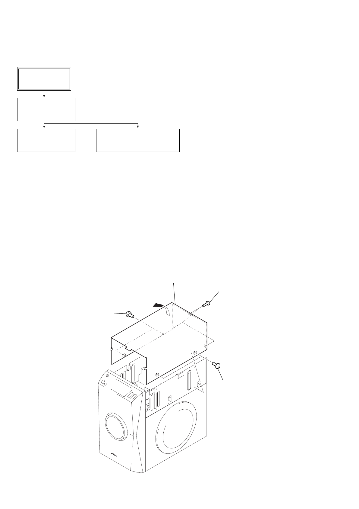
• This set can be disassembled in the order shown below.
3-1. DISASSEMBLY FLOW
Set
3-2. TOP CHASSIS
(Page 6)
SECTION 3
DISASSEMBLY
3-3. DIGITAL BOARD
(Page 7)
Note: Follow the disassembly procedure in the numerical order given.
3-4. FRONT CABINET SECTION
(Page 7)
3-2. TOP CHASSIS
4
top chassis
3
three screws
(BVTP3
×
10)
2
two case screws
1
two case screws
6
3-3. DIGITAL BOARD
)
6
Insert a flat-tip screwdriver into a recess
in the bottom of the set
to raise the front cabinet section a little.
7
Insert the jig
(J-2051-238-A)
into a space made by
inserting the screwdriver,
and raise the front cabinet
section gradually.
8
front cabinet section
boss
boss
boss
1
wire (flat type) (21 core)
(CN801)
2
screw
(BVTP3
×
8)
5
screw
(BVTP3
×
8)
4
screw
(BVTP3
×
8)
3
harnness
Note : Take care not to damage the set by applying an excessive force.
4
1
wire (flat type)
(21 core) (CN801)
5
connector
(CN602)
connector
(CN601)
2
screw
(BVTP3
SS-US501/SW-US501/UZ-US501
3
harness
×
8)
7
two screws
6
(BVTP3
screw
(BVTT3
×
10
×
8)
9
DIGITAL board
3-4. FRONT CABINET SECTION
8
two screws
(BVTP3
×
8)
7
SS-US501/SW-US501/UZ-US501
SECTION 4
TEST MODE
[TEST MODE]
Procedure:
1. Press the I/1 button on the main set once while pressing the
[S-MODE] button on the remote commander (RM-Z7S101)
and the [INPUT] button on the main set.
2. When the test mode is activated, “USB” and “VOL” are
displayed on the liquid crystal display.
3. Press the [VOLUME +] button on the main set, and the display
on liquid crystal display will change over from “VOL” to
“LCD”, “SWP” “ALLOC”, version number, and “VOL” in
this order (in reverse order if the [VOLUME
main set is pressed).
4. Press the [INPUT] button on the main set, and the displayed
test item will start (except version display).
5. Press the I/1 button to turn the power OFF, and the test mode
will be deactivated and the cold reset will be executed.
Test Items:
Item Description
VOLUME TEST The display on liquid crystal display changes
over from “VOL” to “0”, “10”, “20”, “30”, “40”,
and “VOL” in this order, and along with the
change of display, the volume is also changed.
LCD TEST The liquid crystal display all blink, and after 5
seconds, they return to original state.
SWAP (DSP TEST) The input signal is outputted to 5.1ch speakers.
This mode is deactivated if the [INPUT] button
on the main set is pressed again.
KEY ALLOC TEST If the button displayed on the liquid crystal
display is pressed, the next button is displayed.
When all buttons are pressed, the original display
is restored.
Version Display The version number of microcomputer software
is displayed.
-
] button on the
Note: During the test mode, the APC (auto pow er control) turns ON, and
it turns OFF if the [INPUT] button on the main set is not pressed for
5 seconds.
8
SECTION 5
DIAGRAMS
SS-US501/SW-US501/UZ-US501
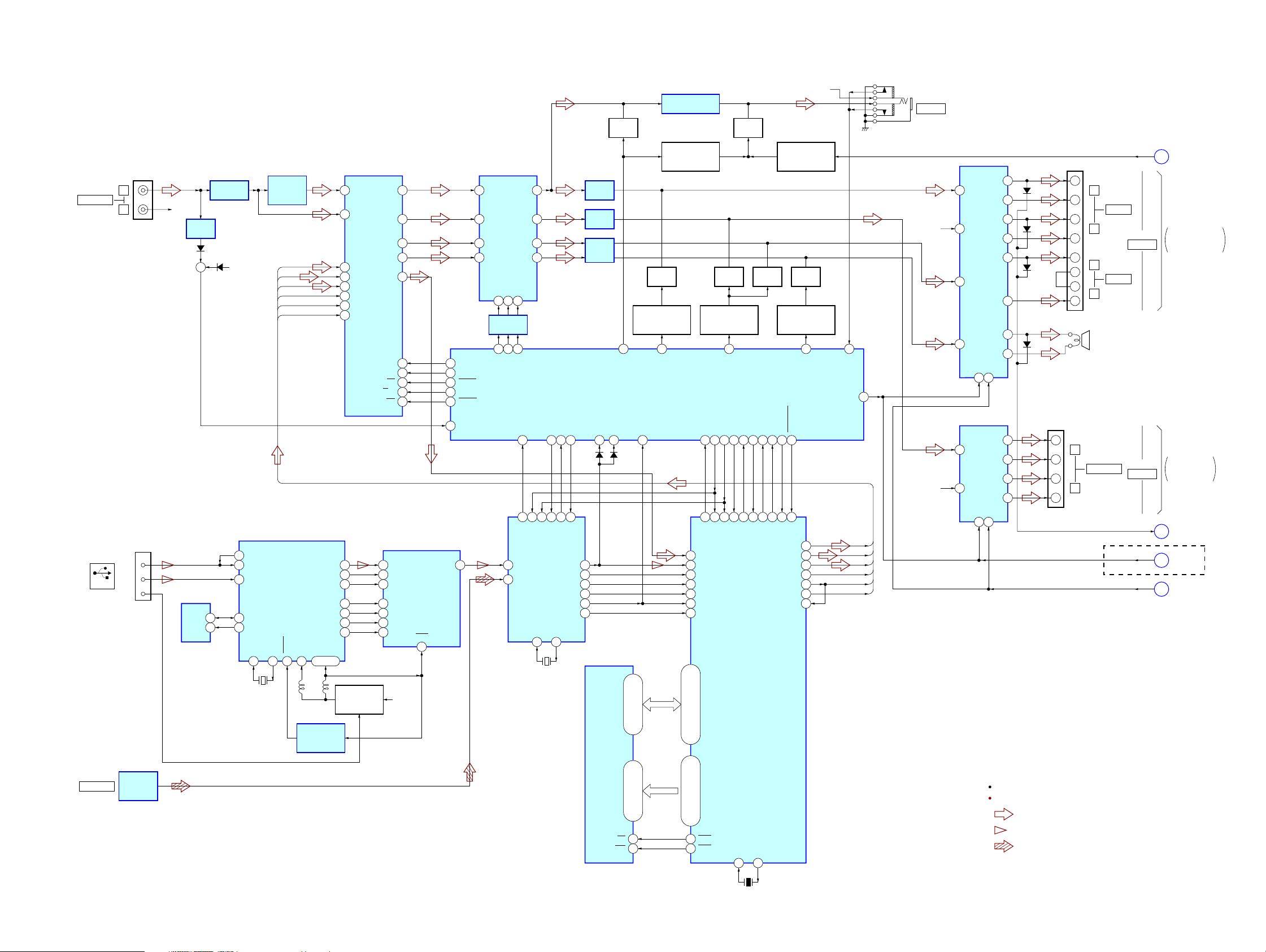
5-1. BLOCK DIAGRAM – MAIN Section –
ANALOG IN
J502
L
R-CHR
D503
BUFFER
IC505
+
LINE AMP
IC508
D504
R-CH
LOW-PASS
FILTER
IC507
SD1
SD3
SD2
BCK
LRCK
MCLKI
CODEC,
A/D, D/A CONVERTER,
IC805
30 4LIN+ LINA
29 LIN–
6 SDTI1
7 SDTI2
8 SDTI3
4 BCLK
5 LRCK
39 MCLKI
27L-OUT 3LOUTA
25SL-OUT
24C-OUT
23SW-OUT
9SDTO
43CDTI
42CCLK
41CS
3S/M
17PD
ELECTRICAL VOLUME
10 LINC
7 LINB
22 RINB
LEVEL SHIFT
1 CO-DI
2 CO-CLK
100 CO-CS
98 CO-S/MUTE
99 CO-PD
IC604
DATA14CK16STB
15
IC601
70
69
VOL-CLK68VOL-STB
VOL-DATA
9LOUTC
6LOUTB
23ROUTB
SYSTEM CONTROLLER
IC802 (1/2)
PRE AMP
IC607
PRE AMP
IC606
PRE AMP
IC608
MUTING
Q613
65
HP MUTE
HEADPHONE AMP
CONTROL SWITCH
Q821, 822
MUTING
Q608
MUTING
CONTROL SWITCH
Q605, 606
27
MUTE-FL, FR
IC605
MUTING
MUTING
Q700
MUTING
Q603
MUTING
CONTROL SWITCH
Q601, 602
28
MUTE-SL, SR, C
MUTING
Q611
R-CH
MUTING
CONTROL SWITCH
Q710, 711
MUTING
Q612
MUTING
CONTROL SWITCH
Q609, 610
29
MUTE-SW
66
HP S/W
44AMP-MUTE
J701
PHONES
R-CH
11
12
POWER AMP
15
14
IC401
MUTE
22
4
ST-BY
HP MUTING
9
D451
7
5
D452
3
17
D453
19
21
D454
23
+
–
+
–
+
–
+
–
L
FRONT
R
L
CENTER
R
SP101
(SUB WOOFER)
J404 (1/2)
SPEAKER
(Page 10)
A
TO FRONT/CENTER
SPEAKER (L)/(R)
(SS-US501)
USB
VBUS
81 AUDIO DEC
USB CODEC
IC501
J501
2
D+
3
D–
4
EEPROM
IC504
SDA
SCL
6 PUR
7 DP
8 DM
41 SDA
5
42 SCL
6
XTALI10MRST
51
50
X501
6MHz
XTALO
AVDD
2
RESET SIGNAL
GENETATOR
36DOUT1 18TX+ 16DATA 25SDO3
34BCK
35LRCK
44MCLKO
15P3.1
24P1.0
19P3.4
DVDD
9, 21, 37
USB ON/OFF
SWITCH
Q501, 502
IC510
DIGITAL AUDIO
TRANSMITTER
IC502
13 SDATA 3 DIN0 30 SDI2
11 SCLK
12 SYNC
6 MCLK
5 CLK0
4 CLK1
3 L
USB
+3.3V
RST
15
DIGITAL AUDIO
INTERFACE RECEIVER
IC801
24
35DO36DI38CL37
4 DIN1
DIR-DO
22
12.288MHz
DIR-XST
DIR-CE
20
19
17
CE
XSTATE
XIN21XOUT
X803
DIR-XMODE
23
D804
48
XMODE
14BCK
15LRCK
13CKOUT
34ERROR
24AUDIO
DIR-AD
22
S-RAM
IC810
DIGITAL DEC
85
D807
D0 – D15A0 – A15
7 – 10, 13 – 16,
DIR-ERR
18
29 – 32, 35 – 38
DSP-DO
DIG-DI
DIG-CLK
DSP-CS
6
35
18 SDI1
29 BCKI2
28 LRCKI2
22 KFSIO
59 EXLOCK
69 GP8
98, 80 – 77, 75 – 72
108, 107, 105 – 102, 99,
14
7
8
13
32
33
34
36
HCS
HDIN
HCLK
HDOUT
AUDIO DIGITAL
SIGNAL PROCESSOR
IC808
D0 – D15A0 – A15
DSP-HACN
DSP-PLOCK
DSP-BST
17
15
7
56
BST
HACN
PLOCK
DSP-GP9
16
12
68
113
GP9
DSP-PM
DSP-RST
11
2
PM
XRST
AMP
IC402
MUTE
1
15
16
11
12
ST-BY
4
2
SURROUND
R-CH
23SDO1
24SDO2
20BCKO
19LRCKO
14SCKOUT
67GP10
SD1
SD2
SD3
BCK
LRCK
MCLK
7
+
L
–
SURROUND
+
R
J404 (2/2)
SPEAKER
TO SURROUND
SPEAKER (L)/(R)
(SS-US501)
–
MTR CTL
(EXCEPT US)
AMP MUTING
STANDBY
B
C
D
(Page 10)
(Page 10)
(Page 10)
OPTICAL IN
OPTICAL
RECEIVER
IC503
5 – 1, 44 – 42,
27 – 24, 21 – 18
6CS
82 – 85, 66 – 64
112, 110, 109, 97 – 92,
44 CS0
45 WE017WE
99
MCLK112MCLK2
9
X804
13.5MHz
R-ch is omitted due to same as L-ch.
SIGNAL PATH
: AUDIO
: USB
: OPTICAL IN
SS-US501/SW-US501/UZ-US501
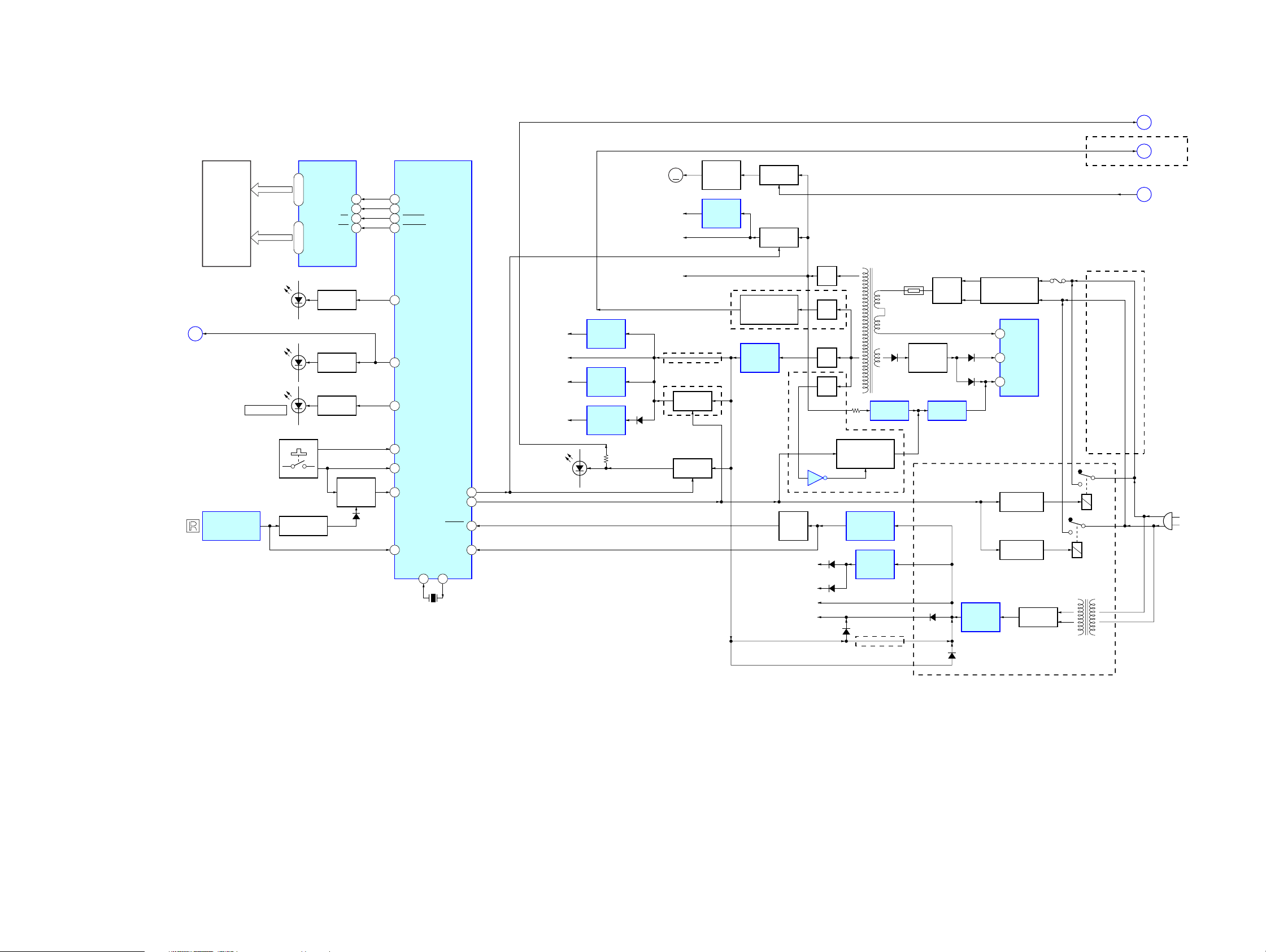
(AC IN)
RECT
D992 – 995
T902
SUB POWER
TRANSFORMER
+5.6V
REGULATOR
IC991
RESET SIGNAL
GENETATOR
IC803
RESET
SWITCH
Q804
RY992
RELAY DRIVE
Q992
RY991
RELAY DRIVE
Q991
F901
LINE FILTER
LF901(EXCEPT US),
LF902
RECT
D902
TH901
3
POWER CONTROL
IC901
D
4
VCC
1
FB/OCP
D906 D907
D905
+20V
REGULATOR
Q901
ISOLATOR
PC901
SWITCHING
IC902
T901
MAIN POWER
TRANSFORMER
(US)
(EXCEPT US)
+3.3V
REGULATOR
IC804
D821
D +3.3V
D822
µCOM +3.3V
µCOM +5V
LED B+
D811, 812
D802, 803
RECT
D911
RECT
D920
RECT
D909
B+ SWITCH
Q451, 452
+10V
REGULATOR
Q453
FAN401
(FAN)
M
B+ SWITCH
Q904, 905
AU +15V
AUDIO +5V
POWER/SURROUND AMP
(IC401, 402) B+
+5V
REGULATOR
IC906
POWER ON/OFF
CONTROL SWITCH
Q902, 906
IC903
(US)
RECT
D914
MUTING
CONTROL SWITCH
Q915
(EXCEPT US)
+5V
REGULATOR
IC905
+2.5V
+2.5V
REGULATOR
IC807
READY +3.3V
READY +5V
+3.3V
REGULATOR
IC806
USB +3.3V
+3.3V
REGULATOR
IC506
B+ SWITCH
Q910, 911
(US)
B+ SWITCH
Q907, 908
(EXCEPT US)
D813
D702, 703
(LCD BACK LIGHT)
( US)
D946
46P-CONT
62READY-H
39X138
X2
X801
16MHz
34
90STOP
RESET
S701 – 705
KEY ACTIVE
SWITCH
Q801, 803
82
KEY1
93
INT
91
SIRCS
83
V/R
D806
SIRCS BUFFER
Q802
REMOTE CONTROL
RECEIVER
IC702
67
APC LED
LED DRIVE
Q702
D705
AUTO POWER
73
STAND BY LED
LED DRIVE
Q705
D707
(STANDBY)
71
POWER LED
LED DRIVE
Q703
D706
(POWER ON)
54 LCD-DATA
8SD
53 LCD-CLK7SCK
56 LCD-CS
9CS
35 LCD-C/D10C/D
11 – 14
COM0 – COM3
15 – 32
SEG0 – SEG17
LCD701
LIQUID
CRYSTAL
DISPLAY
LIQUID CRYSTAL
DISPLAY DRIVER
IC701
SYSTEM CONTROLLER
IC802 (2/2)
D
(Page 9)
STANDBY
B
(Page 9)
MTR CTL
C
(Page 9)
AMP MUTING
(EXCEPT US)
A
(Page 9)
HP MUTING
5-2. BLOCK DIAGRAM – DISPLAY/POWER SUPPLY Section –
1010
SS-US501/SW-US501/UZ-US501
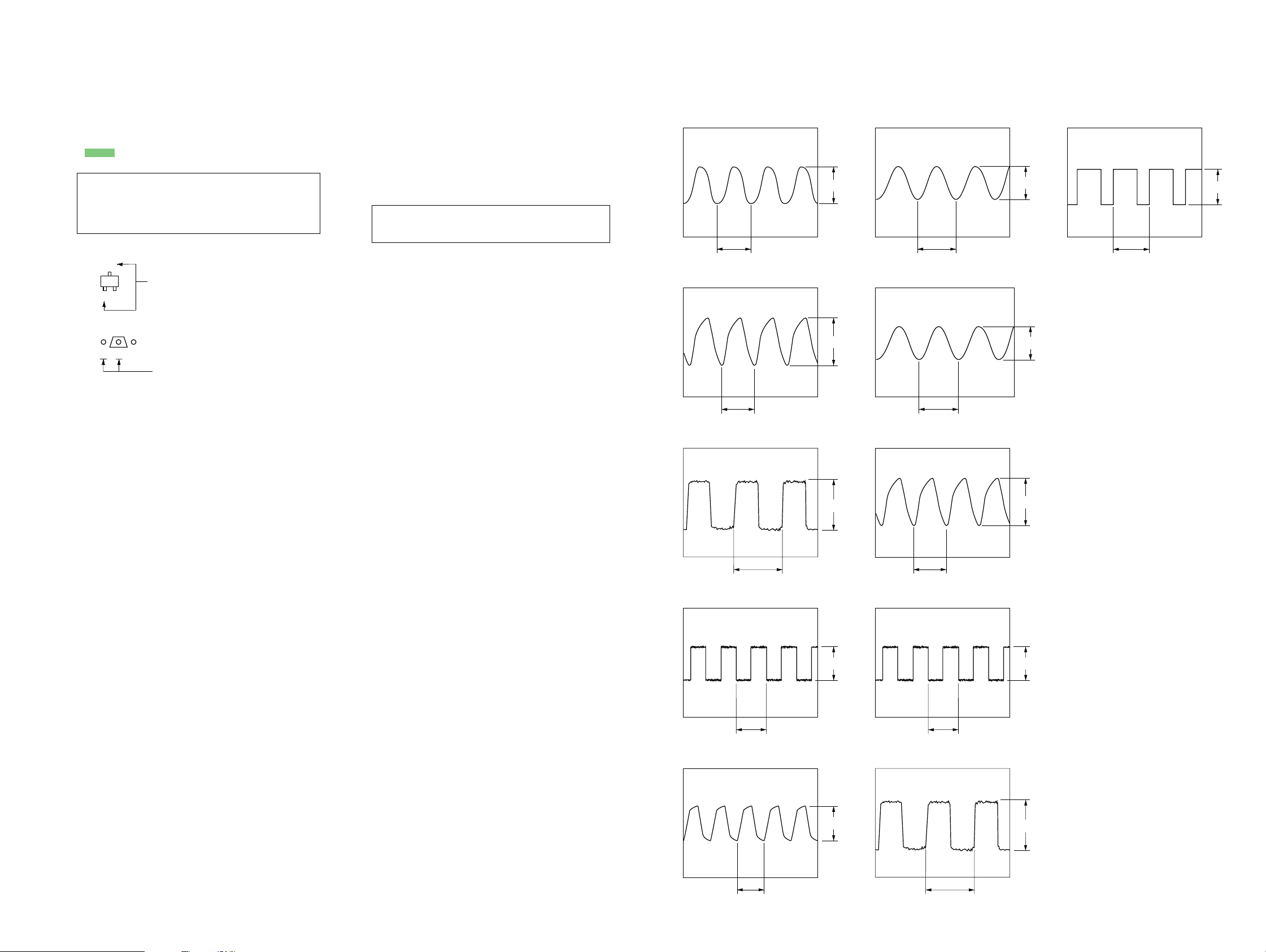
p
p
3.2 Vp-p
326 ns
p
p
p
p
p
p
p
5-3. NOTE FOR PRINTED WIRING BOARDS AND SCHEMATIC DIAGRAMS
Note on Printed Wiring Boards:
• X : parts extracted from the component side.
• Y : parts extracted from the conductor side.
f
•
• : Pattern from the side which enables seeing.
(The other layers' patterns are not indicated.)
Caution:
Pattern face side: Parts on the pattern face side seen from
(Conductor Side) the pattern face are indicated.
Parts face side: Parts on the parts face side seen from
(Component Side) the parts face are indicated.
• Indication of transistor.
: internal component.
C
Q
B
E
B
These are omitted.
Q
CE
These are omitted.
Note on Schematic Diagram:
• All capacitors are in µF unless otherwise noted. pF: µµF
50 WV or less are not indicated except for electrolytics
and tantalums.
• All resistors are in Ω and 1/
specified.
f
•
• 2 : nonflammable resistor.
• C : panel designation.
Note: The components identified by mark 0 or dotted line
• A : B+ Line.
•Voltages and waveforms are dc with respect to ground
•Voltages are taken with a V OM (Input impedance 10 MΩ).
•Waveforms are taken with a oscilloscope.
• Circled numbers refer to waveforms.
• Signal path.
: internal component.
with mark 0 are critical for safety.
Replace only with part number specified.
under no-signal conditions.
no mark : ANALOG
(): USB
[]: OPTICAL
Voltage variations may be noted due to normal production tolerances.
Voltage variations may be noted due to normal production tolerances.
F : AUDIO
N : USB
J : OPTICAL IN
4
W or less unless otherwise
•Waveforms
– DIGITAL Board –
1 IC501 t; (XTALO) (USB mode)
167 ns
2 IC801 qd (CKOUT)
81.4 ns
3 IC801 qf (BCK)
3.1 Vp-
3.1 Vp-
6 IC802 ek (X2)
62.5 ns
7 IC808 qs (MCLK2)
74.1 ns
8 IC808 qf (SCKOUT)
2.3 Vp-
2.6 Vp-
– DISPLAY Board –
qa IC701 2 (OSC2)
3.3 Vp-p
27.4 µs
4 IC801 qg (LRCK)
20.8 µs
5 IC801 wa (XOUT)
3.3 Vp-
3 Vp-
3.6 Vp-
81.4 ns
9 IC808 ql (LRCKO)
3.3 Vp-
20.8 µs
q; IC808 w; (BCKO)
3.4 Vp-
81.4 ns
326 ns
1111
SS-US501/SW-US501/UZ-US501
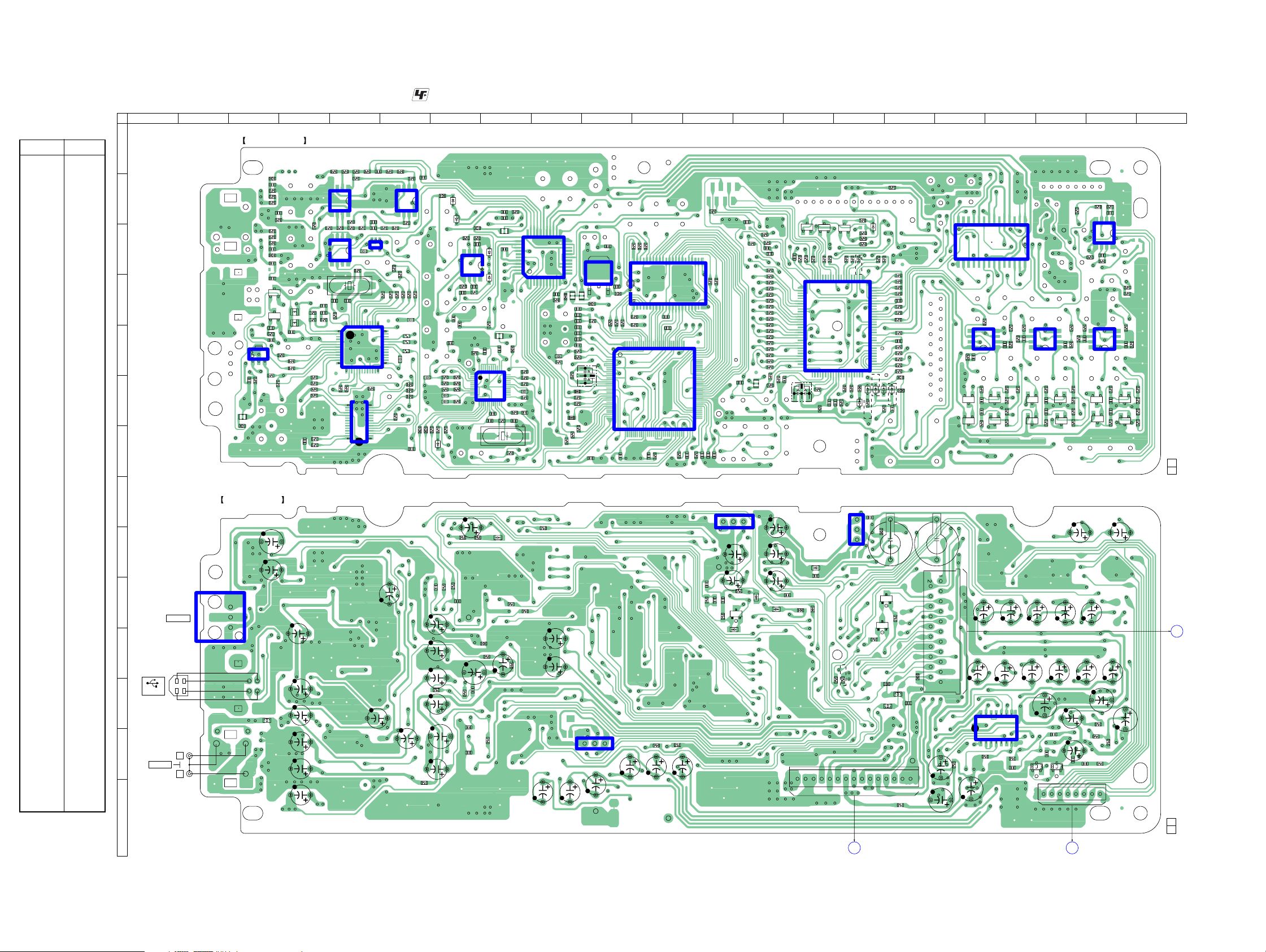
5-4. PRINTED WIRING BOARD – DIGITAL Board – :Uses unleaded solder.
• Semiconductor
Location
Ref. No. Location
D503 C-8
D504 D-8
D802 F-15
D803 F-15
D804 G-7
D805 K-13
D806 C-15
D807 I-8
D808 F-15
D811 F-15
D812 F-16
D813 B-7
D814 B-7
D820 I-14
D821 J-13
D822 J-13
IC501 E-5
IC502 F-5
IC503 J-2
IC504 C-5
IC505 C-7
IC506 C-5
IC507 B-6
IC508 B-5
IC510 E-3
IC601 L-18
IC604 C-18
IC605 C-20
IC606 E-19
IC607 E-20
IC608 E-17
IC801 F-8
IC802 D-15
IC803 H-13
IC804 I-15
IC805 C-9
IC806 M-10
IC807 C-10
IC808 F-11
IC810 D-11
Q501 D-3
Q502 D-3
Q601 F-18
Q602 F-18
Q603 F-19
Q604 F-19
Q605 F-20
Q606 F-20
Q607 F-20
Q608 F-20
Q609 F-17
Q610 F-17
Q611 F-18
Q612 F-18
Q613 M-19
Q614 M-19
Q801 C-15
Q802 C-14
Q803 C-14
Q804 J-13
Q821 J-16
Q822 J-15
1 2 3 4 5 6 7 8 9 10 11 12 13 14 15 16 17 18 19 20 21
A
B
C
D
E
F
G
H
I
IC503
J
IC503
OPTICAL IN
K
J501
124
3
USB
L
M
J502
ANALOG IN
L
R
N
DIGITAL BOARD
FB503
C519
C512
C550
R501
C505
13
FL507
FB508
IC510
R590
C560
R580
DIGITAL BOARD
C561
C534
1
3
L505
FB504
C515
R529
R525
R524
C531
R577
R526
R527
R528
C514
Q501
E
1
0
5
L
Q502
2
0
5
E
L
C504
R503
R504
R505
R508
R509
R543
R506
R544
C518
(CONDUCTOR SIDE)
(COMPONENT SIDE)
R569
R570
R571
R573
14
R578
IC508
85
R564
R561
R560
R562
14
IC504
85
R581
X501
C502
C507
C506
R511
1
0
3
5
1
C
5
R
R510
R512
1
R551
R552
C837
C503
C525
C532
C533
C528
IC501
13
0
2
5
R
1
2
5
R
15
28
IC502
R575
R576
R572
C529
C526
R568
R563
C527
13
IC506
54
C570
R579
4052
2614
R531
14
1
C510
C509
C530
R574
14
FB828
D813
IC507
R597
C831
FB831
R596
D814
R553 R555
4
IC505
5
R559
C583
C857
C859
C842
R808
R809
R806
R807
R805
R804
C835
C834
R803
FB832
IC801
R812
R811
R813
D804
R814
R802
R801
C833
C879
C581
C850
C580
85
R565
R567
R517
R516
R518
R519
R537
R514
R515
C508
39
R532
R533
R534
C511
27
R591
R592
R593
R594
C513
C843
C858
C523
C520
C584
C524
C849
R557
C826
FB826
R824
1
12
C838
C817
R816
C860
C582
R595
1
8
C551
R558
FB830
FL806
33 23
C552
34
C884
3
0
5
D
D504
44
111
R838
FL804
C844
C836
D807
R542
R598
C847
FB834
3748
R823
36
R821
R820
C840
25
R819
2413
R818
C832
R815
C839
X803
R817
R822
R826
C540
R539
IC805
C885
R827
R810
C856
22
12
FL822
C890
FB823
C814
2
9
8
C
2
2
8
C
C811
R830
1
3
8
R
6
3
8
5
R
3
8
R
C894
C888
C855
FL821
1
4
2
8
C
C891
C823
R829
R828
X804
FB821
R832
R833
FB824
4
3
8
R
C862
13
IC807
FB822
R842
IC806
C854
0
1
1
R
IC810
IC808
R840
R122
C852
R107
221
C881
C893
221
91120
90
61
6131
9
9
8
R839
R841
C
C897
IC803
C807
R864
R121
C851
C801
R845
8
9
1
1
1
1
R
R
C804
C813
C895
13
C896
C803
C882
R871
C815
Q804
E
R865
D805
R104
R844
C830
C602
R846
R847
R848
R849
R850
R851
R852
R853
R854
R855
R856
R857
R858
R859
R860
R861
R862
R866
R863
C818
R108
FL802
C845
C819
C802
D821
C805
D822
R895
Q803
Q802
Q801
E
E
C848
R106
R899
R105
R898
R893
1
E
R894
(EXCEPT US)
R891
R892
D806
R897
R896
R888
R890
81100
80
IC802
30
X801
R867
C806
R870
C827
FB809
IC804
D820
C880
FB805
FB808
(US)
R889
CN602
51
5031
R869
D802
R868
D811
FB801
R873
D808
(US)
C820
3
FB804
1
Q822
R120
R825
AMP BOARD
C
CNP423
1
2
1
1
1
1
R
R
C887
C889
3
FB825
7
6
5
1
1
1
1
1
1
R
R
R
R113
R114
1
30
C812
C898
C853
R605
R887
R886
R885
R884
R883
C810
R882
R881
R880
R879
C809
R874
R875
R876
R877
R878
FB803
(EXCEPT US)
FB810
(EXCEPT US)
D812
D803
6
8
8
R872
C
++
C808
Q821
E
R843
E
FB806
FB807
L802
L801
C651
151
R670
14 1
CN801
20
21
IC604
15 28
R644
C870
IC608
5
8
R645
Q610
Q609
C636
C635
R661
Q612
C643
C642
Q611
R659
C637
14 8
4
1
C632
R642
R636
5
R643
8
R637
C624
C634
R664
R663
R662
Q602
R660
Q601
R658
C625C633
C623
IC601
17
R601
R629
R628
C607
C613
C670
C601
Q613 Q614
IC606
R649
C639
C638
R647
C609
C604
C606
R630
R684
R632
R634
5
4
R640
R635
8
1
C622
R641
C630
IC607
R651
Q604
EEEE
Q603
C620
Q606
R650
E
R648
Q605
R646
C619
C631
C621
C629
C681
C616
R685
R682
C680
C605
R602
C603
CN601
AMP BOARD
B
CNP401
C618
R633
R655
C640
R653
R680
81
(Page 20)(Page 20)
R631
C617
14
IC605
85
R638
4
C627
1
R639
EEEEEE
Q608
C641
E
Q607
1-860-901-11(11)
C644
C626
C608
1-860-901-
R665
R666
R657
R656
R654
R652
A
DISPLAY
BOARD
CN702
(Page 18)
11
(11)
1212
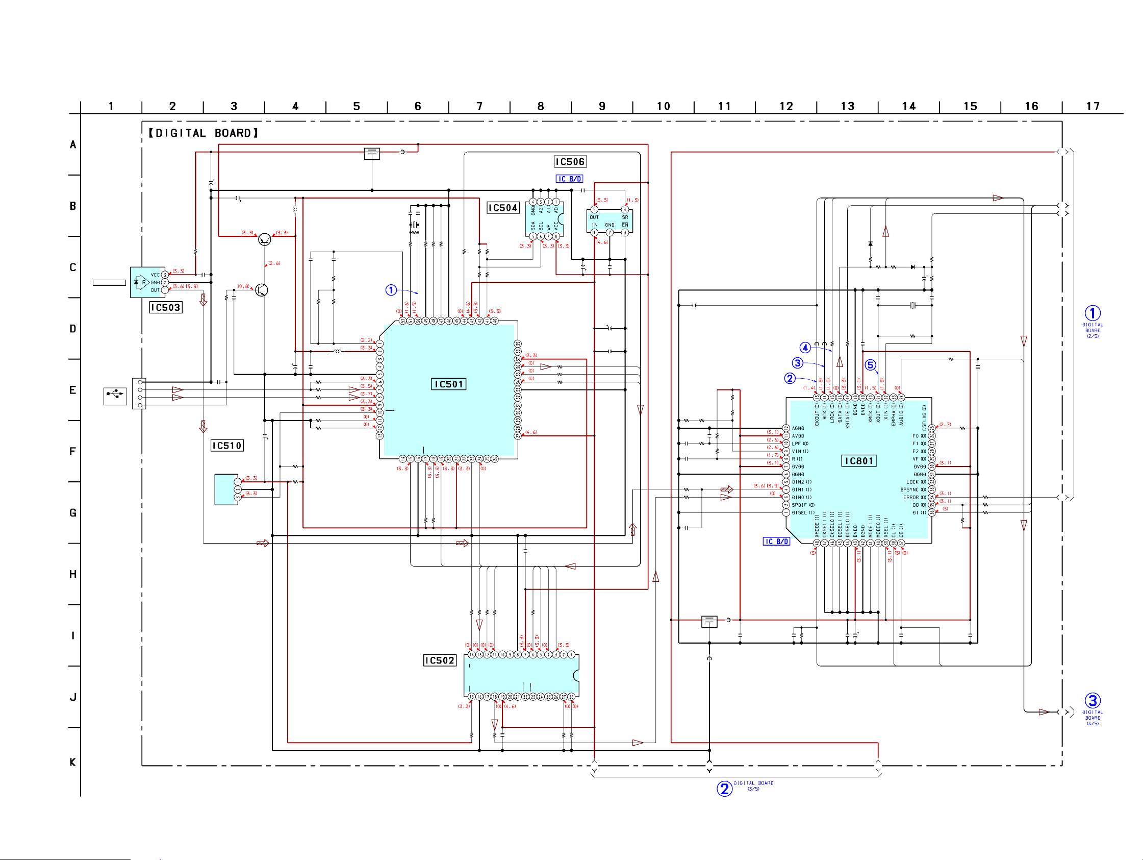
5-5. SCHEMATIC DIAGRAM – DIGITAL Board (1/5) – • See page 11 for Waveforms. • See page 23 for IC Block Diagrams. • See page 26 for IC Pin Function Description.
(1/5)
SS-US501/SW-US501/UZ-US501
IC503
OPTICAL IN
FL507
C561
470
16V
C837
47
35V
Q501
R501
220k
C505
0.1
RESET SIGNAL
GENERATOR
IC510
M62703ML
Q501,502
USB ON/OFF
SWITCH
VIN
GND
RST
2SA1182
C550
0.1
R580
IC503
TORX141L
OPTICAL
RECEIVER
GND
1
J501
USB
D+
D-
VBUS
4
10
C560
0.1
L501
4.7µH
C502 C501
100p 0.001
R512
Q502
2SC2712
C503
47
35V
C534
1
50V
R590
1k
R506
0
2.2k
R511R510
910910
L502
4.7µH
C504
0.1
R503
1.5k
R504
22
R505
22
4.7k
R508
4.7k
R509
PLLFILO
AVDD
PWMO
PLLO
DVSS
PUR
DP
DM
DVDD
MRST
TEST
EXTEN
RSTO
FB508
C507
18p
C506
18p
X501
0
6MHz
R581
1M
R579
R513
220
PLL
FILI
AVSS
XTALI
XTALO
DVSS
P3.1
P3.0
XINT
4.7k
R520
0
0
R514
R515
MCLKI2
USB CODEC
TUSB3200ACPAH
P3.3
4.7k
R521
MCLK
EEPROM
IC504
AT24C64N
R517
R516R537
4.7k100
4.7k
R519R518
100100
SDIN1
SCL
CLKI
DVSS
CLKO2
M
M
IC501
P3.5
P3.4
DVDD
SDA
CLKO
DVDD5
M
NC
PLLOEN
CRESET
DOUT2
DVDD
DOUT1
LRCK
BCK
DVSS
P1.7
P1.6
P1.5
P1.4
P1.3
DVDD5
P1.2
P1.1
P1.0
+3.3V REGULATOR
C509
4.7
50V
R532
R533
R534
C570
0.1
75
100
100
IC506
TPS78833DBVR
BCK
LRCK
CKOUT
C508
0.1
C862
47p
C510
22
25V
C511
0.1
SDATA
SYNC
SCLK
R804 R805
22k 10k
C834 R803
0.1 100
C833
0.1
R802
100
R801
100
C879
33p
R807
4.7k
R806
1k
R809
C835
1k
0.01
R808
4.7k
FB831
FB832
100
R811
820
D804
1SS355
R813 R814 R816
1k 100 1k
0.1
100
C836
R812
DIGITAL AUDIO
INTERFACE RECEIVER
IC801
LC89056W
822
SDI2
D807
1SS355
C838 C839
47p 22p
X803
12.288MHz
885
R810
100
C817
R817
1
1M
50V
R815
1M
AUDIO
R818
100
C832
100p
R819
1k
100
R820
100
R821
824
100
R822
R823
10k
DI
A1
A2
A3
A4
(Page 14)
C513
CLK0
L
DIGITAL
AUDIO
TRANSMITTER
IC502
DIT4096
CLK1
SCLK
SYNC
SDATA
0
4.7k
4.7k
0
R591
R531
R593
R592
/S
M
SCLK
SYNC
SDATA
ST
TX+
TX-
DGND
R
0.1
L
CLK0
CLK1
MCLK
0
R594
T0
T1
VIO
FM
FM
DGND
DAT
ONO
M
VDD
M
AUDIO
L
CLK
M
PH
EM
CSS
CLK1
CLK0
COPY/C
ODE
M
U
V
BLS
BLSM
R551 R552C518R544R543
4.7k 10k0.1100100
B1
FB830
FL804
FB834
C831
0.01 0.01 10k 0.1
B2
C844 R824 C842
XMODE
C843
220
10V
C847
0.001
CL
C840
0.1
CE
C1
(Page 16)
B3
(Page 15)
1313
SS-US501/SW-US501/UZ-US501
5-6. SCHEMATIC DIAGRAM – DIGITAL Board (2/5) – • See page 11 for Waveform. • See page 26 for IC Pin Function Description.
(2/5)
A1
VR
881
KEY
885
R888
R894
100k
(EXCEPT US)
R890
47k
10k
R887
10k
(US)
R825
1k
R886
R885
R884
R883
R879
R878
R877
R876
R875
R874
100
C809
0.1
(Page 13)
Q801
D806
R897
1SS355
100k
Q802
2SC2712
A2
A3
R105
1k
898
R106
1k
899
900
802
100p
100p
100p
C848
C830
C602
DI
CL
R826
100
CE
820
822
XMODE
824
A4
C801
0.1
SIRCS
BUFFER
R899
1k
R844
1k
1k
R845
R104
100k
806
807
808
811
812
813
814
815
816
817
827
828
829
100
R846
100
R847
100
R848
100
R849
100
R850
100
R851
100
R852
100
R853
1k
R854
1k
R855
100
R856
1k
R857
1k
R107
1k
R858
1k
R859
1k
R860
1k
R861
1k
R862
DTA114TKA-T
R896
100k
R898
470k
Q803
2SC2712
Q801,803
KEY ACTIVE
SWITCH
R895
47k
SIRCS
R892 R891
100k 100k
47k
R893
SYSTEM CONTROLLER
IC802
µPD703033BYGF
-M53-3BA-A
HEAD PHONE BUS
HP MUTE
(Page 17)
CN801
HP.L
A-GND
HP.R
HP S/W
856
855
100k
100k
100k
100k
STND
R882
1k
R881
1k
R880
1k
100
1k
1k
1k
1k
C870
0.22F
5.5V
PWR
870
869
868
APC
HP S/W
862
856
855
854
853
C810
0.1
R889
10k
FB808
D821
1SS355
854
853801
SIRCS
APC
VR
KEY
STND
PWR
1µH
L802
FB807
FB806
1µH
L801
Q821
SRA2203S/F
Q821,822
MUTING
CONTROL
R120
100k
C802
SWITCH
Q822
2SC2712
22
25V
HP.L
GND
HP.R
HP.SW
HP-MUTE
LCD-CS
LCD-C/D
LCD-DATA
LCD-CLK
SIRCS
APC LED
V/R
KEY
STAND BY LED
POWER ON LED
STAND BY 5.6V
BACK LIGHT
D-3.3V
GND
READY 3.3V
GND(SHIELD)
R843
1k
21P
(Page 19)
D2
D1
(Page 15)
C805
Q804
2SC2712
RESET
SWITCH
R871
100
C845
22
25V
(EXCEPT US)
D811 D812
1SS355 1SS355
1SS355
D802
(US)
R873
0
FB801
R863
1k
0.1
C804
R108
0.001
1k
D
R865 C815
10k 0.22
D805
R864C882
1SS355
47k0.01
T
S
R
C807
0.1
RESET SIGNAL
N
IN
G
V
C819
1
50V
GENERATOR
IC803
PST592C
R872
100
C818
1
R866
10k
R868 R869
X801
16MHz
844
C806
0.1
C827
0.1
100 100
846
D808 R870
1SS355 100
C803
220
10V
FB805 D822
+3.3V REGULATOR
C808
0.22F
5.5V
C886C880 D820
0.11 1SS355
R867
1M
FB809
FB804
IC804
S-81233SGY
1SS355
FL802
C820
0.1
5.6V UNSW FOR SUB
FB810
STAND BY 5.6V
DIGITAL 5.6V-SW
FB803
1SS355
D803
829
828
827
AU 15V S/W
SW-MUTE
SL, SR, C-MUTE
FL,FR-MUTE
(Page 17)
E2
E1
E3
E4
E5
(Page 16)
1414
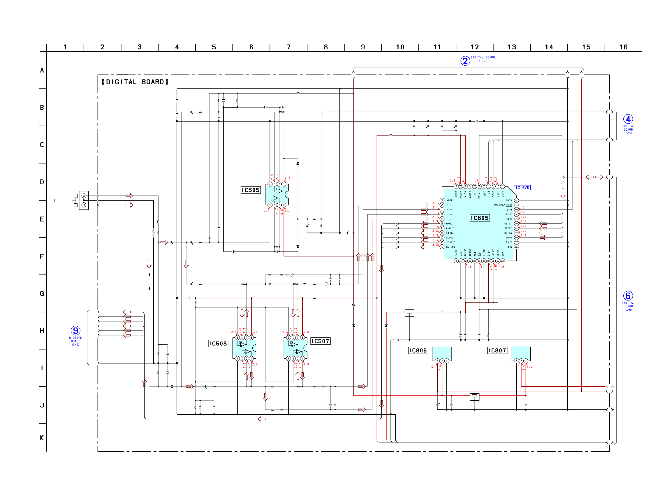
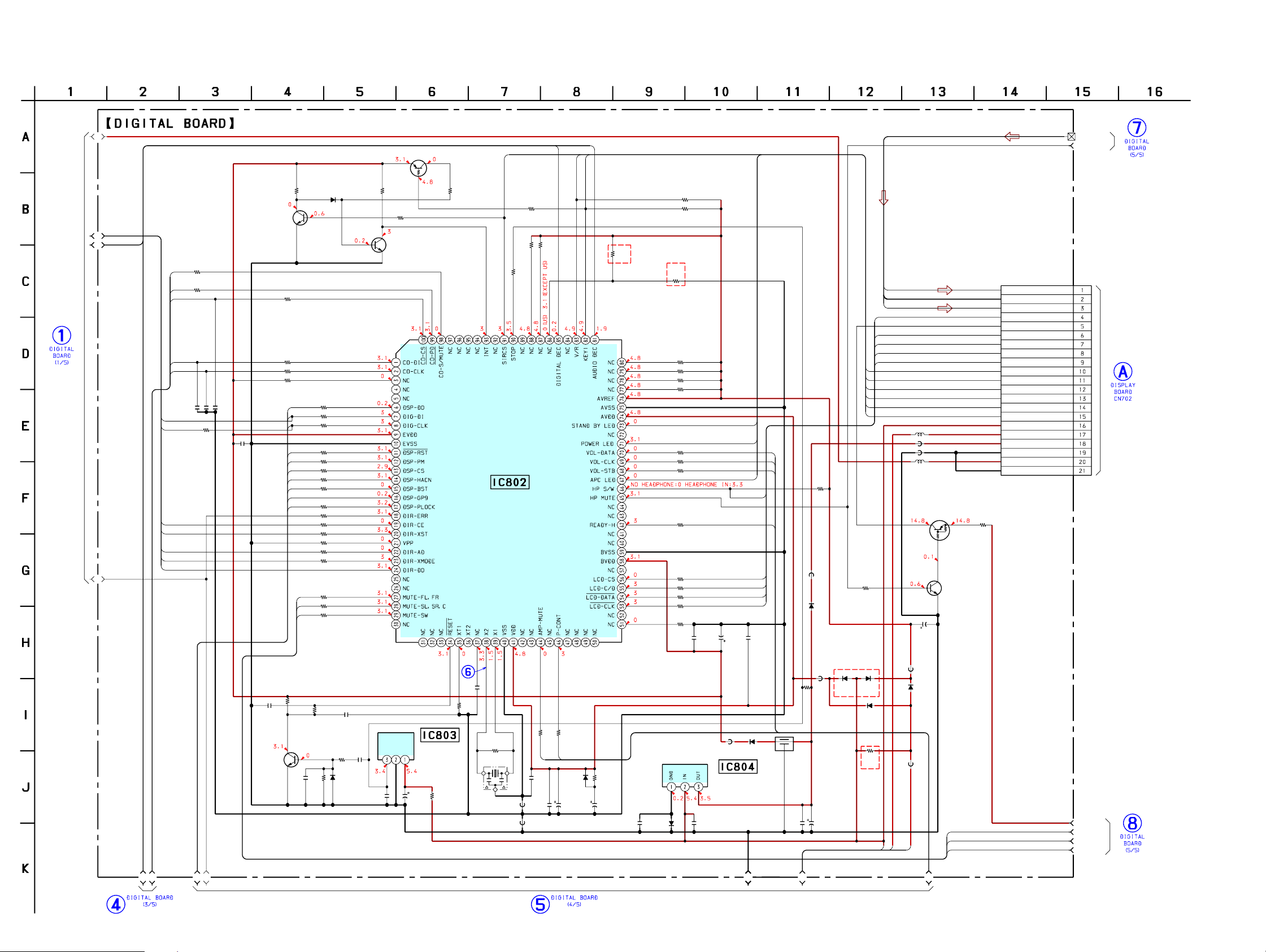
5-7. SCHEMATIC DIAGRAM – DIGITAL Board (3/5) – • See page 23 for IC Block Diagram.
(3/5)
SS-US501/SW-US501/UZ-US501
(Page 13)
B3
B1
B2
ANALOG IN
C540
C512
0.1
C519
0.1
J502
2P
R
L
µH
4.7
R526
10k
L505
R527
0
FB503
C520
C523
1
50V
R595
100k
R553
10k150V
C580
220p
C582
220p
R596R559
100k10k
R539
1
4.7k
50V
BUFFER
IC505
NJM4565M
C581 C552
0.1 0.001
GND
R558
330k
C551C583
0.0010.1
R542
4.7k
R555
330k
D503
1SS355
VDD
C524
1
50V
D504
1SS355
881
R838
10
R598
0
R557
220k
C584
100
10V
C856
C-28
C855
C-27
C854
C-26
C853
C-25
C852
C-24
C851
C-23
C860
C859 C857
470
0.1 0.1
16V
4.7 50V
4.7 50V
4.7 50V
4.7 50V
4.7 50V
4.7 50V
C858
22
25V
C884
0.1
CODEC,
A/D,D/A CONVERTER
IC805
AK4527B
SOUT
899
801
802
900
LRCKO
SDT11
SDT12
SDT13
898
BCKO
SDI1
D1
D2
F1
(Page 14)
(Page 17)
A-GND
R562 R563
R524
10k
R525
0
SW
C
SL
SR
L
R
C-23
C-24
C-25
C-26
C-27
C-28
C514R528
220p22k
C515R529
220p22k
FB504
C525
22
R560
25V
47k
R578
C533
4.7k
100
10V
VDD
LINE AMP
IC508
NJM4565M
R569 R570
C528
47k 22k
22
25V
C532
R577
4.7k
C531
10
0.1
50V
GND
220 100
R564
10k
R573
10k
R571 R572
220 100
R565 R567 R568R561 C527
10k 220 10022k 470p
R597
47
VDD
LOW-PASS
GND
R574
10k
FILTER
NJM4565M
IC507
C526
0.001
FB828
FL806
FB826
(Page 16)
D814D813
1SS3551SS355
C850
C826
0.1
T
D
U
N
IN
O
G
V
IC806
S-81233SGY
R576R575
100220
C529
C530
0.001
470p
V
C888
22
25V
C849
470
0.1
16V
C887
0.1
FL821
R827
C885
100k
0.1
T
D
U
N
IN
+2.5V REGULATOR+3.3V REGULATOR
TA48M025F
IC807
O
V
V
G
F2
F3
C890
0.1
F4
READY 5.6V
A-GND
A-GND
AUDIO 5V
F5
1515
 Loading...