Sony SSTSL-10 Service manual
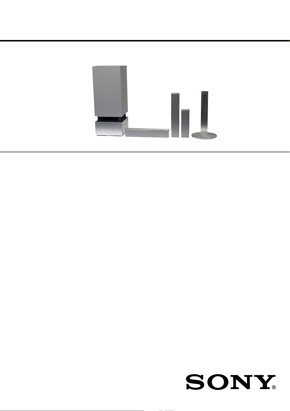
SA-WSLF10/
SS-CTL10/TSL10/TSL11
SERVICE MANUAL
Ver. 1.0 2005.03
SA-WSLF10 SS-CTL10 SS-TSL10 SS-TSL11 STAND ASSY
• SA-WSLF10 is the subwoofer in DAV-LF10.
• SS-CTL10 is the center speaker in DAV-LF10.
• SS-TSL10 is the front speaker in DAV-LF10.
• SS-TSL11 is the surround speaker in DAV-LF10.
US Model
E Model
Australian Model
This system incorporates with Dolby* Digital and Dolby Pro Logic (II)
adaptive matrix surround decoder and the DTS** Digital Surround
System.
* Manufactured under license from Dolby Laboratories.
“Dolby”, “Pro Logic”, and the double-D symbol are trademarks of
Dolby Laboratories.
**Manufactured under license from Digital Theater Systems, Inc.
“DTS”, “DTS-ES”, and “DTS Digital Surround” are trademarks of
Digital Theater Systems, Inc.
For the US model
AUDIO POWER SPECIFICATIONS
POWER OUTPUT AND
TOTAL HARMONIC
DISTORTION: With 4 ohm loads, both
Amplifier section SA-WSLF10
Stereo mode (rated) 86 W + 86 W (4 ohms at
Surround mode (reference) music power output
*Depending on the sound field settings and the source,
there may be no sound output.
Inputs VIDEO/SAT:
channels driven, fro m
200 – 20,000 Hz; rated
65 watts per channel
minimum RMS power,
with no more than 0.7 %
total harmonic distortion
from 250 milli watts to
rated output.
1 kHz, THD 10 %)
86
W (each)
Front:
(with SS-TSL10)
86
Center*:
(with SS-CTL10)
Surround*:
(with SS-TSL11)
Subwoofer*:
(with SA-WSLF10)
Sensitivity: 300 mV
Impedance: 50 kilohms
W
86
85
W
W × 2
SPECIFICATIONS
Phones Accepts low-and high-
impedance headphones.
Tuner section SA-WSLF10
System PLL quartz-locked digital
synthesizer system
FM tuner section
Tuning range
North American models: 87.5 – 108.0 MHz
(100 kHz step)
Other models: 87.5 – 108.0 MHz
(50 kHz step)
Antenna (aerial) FM wire antenna (aerial)
Antenna (aerial) terminals 75 ohms, unbalanced
Intermediate frequency 10.7 MHz
AM tuner section
Tuning range
North American models: 530 – 1,710 kHz (with the
interval set at 10 kHz)
531 – 1,710 kHz (with the
interval set at 9 kHz)
Other models: 530 – 1,710 kHz (with the
interval set at 10 kHz)
531 – 1,602 kHz (with the
interval set at 9 kHz)
Antenna (aerial) AM loop antenna (aerial)
Intermediate frequency 450 kHz
Video section SA-WSLF10
Outputs Video: 1 Vp-p 75 ohms
Inputs
Speakers
Fro
nt SS-TSL10
Speaker system Two-way bass reflex,
Speaker unit 50 mm (2 inches) dia. cone
Rated impedance 4 ohms
Dimensions (approx.) 68 × 380 × 53 mm (2
S video:
Y: 1 Vp-p 75 ohms
C: 0.286 Vp-p 75 ohms
COMPONENT:
Y: 1 Vp-p 75 ohms
P
B/CB
, PR/CR: 0.7 Vp-p
75 ohms
Video: 1 Vp-p 75 ohms
magnetically shielded
type × 2, 25 mm (1 inch)
dia. balance-dome-type
tweeter
3
1
/8 inches) (w/h/d)
15 × 2
220 × (398 – 530) × 220
3
mm (8
/4 × (15 3/4 – 20 7/8)
3
/4 inches) (w/h/d ) with
× 8
stand
– Continued on next page –
/4 ×
SPEAKER SYSTEM
9-879-563-01
2005C05-1
© 2005.03
Sony Corporation
Audio Group
Published by Sony Engineering Corporation
SA-WSLF10/SS-CTL10/TSL10/TSL11
r
Mass (approx.) 1.3 kg (2 lb 14 oz)
Center SS-CTL10
Speaker system Two-way bass reflex,
Speaker unit 50 mm (2 inches) dia. cone
Rated impedance 4 ohms
Dimensions (approx.) 68 × 380 × 53 mm (2
Mass (approx.) 1.3 kg (2 lb 14 oz)
Surround SS-TSL11
Speaker system Two-way bass reflex,
Speaker unit 50 mm (2 inches) dia. cone
Rated impedance 4 ohms
Dimensions (approx.) 68 × 240 × 53 mm (2
Mass (approx.) 1.0 kg (2 lb 4 oz)
Subwoofer SA-WSLF10
Speaker system Bass reflex
Speaker unit 180 mm (7
Rated impedance 4 ohms × 2
Dimensions (approx.) 241 × 606 × 241 mm
Mass (approx.) 14 kg (30 lb 14 oz)
Power requirements
North American models: 120 V AC, 60 Hz
Taiwan model: 120 V AC, 50/60 Hz
Other models: 220-240 V AC, 50/60 Hz
Power consumption 120 W
2.7 kg (6 lb) with stand
magnetically sh ie lded
type ×2, 25 mm (1 inch )
dia. balance-dome-type
tweeter
3
1
/8 inches) (w/h/d)
15 × 2
magnetically sh ie lded
type ×2, 25 mm (1 inch )
dia. balance-dome-type
tweeter
1
/2 × 2 1/8 inches) (w/h/d)
9
1
cone type
1
/2 × 23 7/8 × 9 1/2
(9
inches) (w/h/d)
0.3 W (at the Power Saving
mode)
/4 ×
3
/4 ×
/8 inches) dia.
Notes on chip component replacement
• Never reuse a disconnected chip component.
• Notice that the minus side of a tantalum capacitor may be
damaged by heat.
SAFETY CHECK-OUT
After correcting the original service problem, perform the following
safety check before releasing the set to the customer:
Check the antenna terminals, metal trim, “metallized” knobs, screws,
and all other exposed metal parts for AC leakage.
Check leakage as described below.
LEAKAGE TEST
The AC leakage from any exposed metal part to earth ground and
from all exposed metal parts to any exposed metal part having a
return to chassis, must not exceed 0.5 mA (500 microamperes.).
Leakage current can be measured by any one of three methods.
1. A commercial leakage tester , such as the Simpson 229 or RCA
WT -540A. Follow the manuf acturers’ instructions to use these
instruments.
2. A battery-operated A C milliammeter . The Data Precision 245
digital multimeter is suitable for this job.
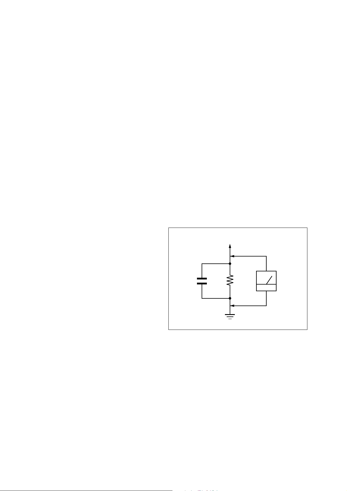
3. Measuring the voltage drop across a resistor by means of a
VOM or battery-operated AC voltmeter . The “limit” indication
is 0.75 V, so analog meters must have an accurate lo w-voltage
scale. The Simpson 250 and Sanwa SH-63Trd are examples
of a passive VOM that is suitable. Nearly all battery operated
digital multimeters that have a 2 V AC range are suitable. (See
Fig. A)
To Exposed Metal
Parts on Set
Design and specifications are subject to change
without notice.
AC
0.15 µF
1.5 k
Ω
voltmete
(0.75 V)
Earth Ground
Fig. A. Using an AC voltmeter to check AC leakage.
SAFETY-RELATED COMPONENT WARNING!!
COMPONENTS IDENTIFIED BY MARK 0 OR DOTTED LINE
WITH MARK 0 ON THE SCHEMATIC DIAGRAMS AND IN
THE PARTS LIST ARE CRITICAL TO SAFE OPERATION.
REPLACE THESE COMPONENTS WITH SONY PARTS WHOSE
PART NUMBERS APPEAR AS SHOWN IN THIS MANUAL OR
IN SUPPLEMENTS PUBLISHED BY SONY.
2
SA-WSLF10/SS-CTL10/TSL10/TSL11
SECTION 1
SERVICING NOTES
TABLE OF CONTENTS
1. SERVICING NOTES ............................................... 3
2. GENERAL ................................................................... 6
3. DISASSEMBLY ......................................................... 7
4. ELECTRICAL ADJUSTMENT ............................ 8
5. DIAGRAMS
5-1. Block Diagram – AUDIO DSP Section –........................ 9
5-2. Block Diagram – AUDIO Section –................................ 10
5-3. Block Diagram
– VIDEO/POWER SUPPLY Section – ........................... 11
5-4. Printed Wiring Board
– MAIN Board (Component Side) – ............................... 14
5-5. Printed Wiring Board
– MAIN Board (Conductor Side) – ................................. 15
5-6. Schematic Diagram – MAIN Board (1/4) – .................... 16
5-7. Schematic Diagram – MAIN Board (2/4) – .................... 17
5-8. Schematic Diagram – MAIN Board (3/4) – .................... 18
5-9. Schematic Diagram – MAIN Board (4/4) – .................... 19
5-10. Printed Wiring Board
– S-MASTER Board (Component Side) – ...................... 20
5-11. Printed Wiring Board
– S-MASTER Board (Conductor Side) –........................ 21
5-12. Schematic Diagram – S-MASTER Board (1/4) – ........... 22
5-13. Schematic Diagram – S-MASTER Board (2/4) – ........... 23
5-14. Schematic Diagram – S-MASTER Board (3/4) – ........... 24
5-15. Schematic Diagram – S-MASTER Board (4/4) – ........... 25
5-16. Printed Wiring Board – TX Board –................................ 26
5-17. Schematic Diagram – TX Board – .................................. 27
5-18. Printed Wiring Board – VIDEO I/O Board – .................. 28
5-19. Schematic Diagram – VIDEO I/O Board – ..................... 29
5-20. Printed Wiring Boards
– COMPONENT/SPK-OUT Boards –............................ 30
5-21. Schematic Diagram
– COMPONENT/SPK-OUT Boards –............................ 31
5-22. Printed Wiring Boards – POWER SUPPLY Section –.... 32
5-23. Schematic Diagram – POWER SUPPLY Section – ........ 33
UNLEADED SOLDER
Boards requiring use of unleaded solder are printed with the leadfree mark (LF) indicating the solder contains no lead.
(Caution: Some printed circuit boards may not come printed with
the lead free mark due to their particular size)
: LEAD FREE MARK
Unleaded solder has the following characteristics.
• Unleaded solder melts at a temperature about 40 ˚C higher
than ordinary solder.
Ordinary soldering irons can be used but the iron tip has to be
applied to the solder joint for a slightly longer time.
Soldering irons using a temperature regulator should be set to
about 350 ˚C.
Caution: The printed pattern (copper foil) may peel away if
the heated tip is applied for too long, so be careful!
• Strong viscosity
Unleaded solder is more viscou-s (sticky, less prone to flow)
than ordinary solder so use caution not to let solder bridges
occur such as on IC pins, etc.
• Usable with ordinary solder
It is best to use only unleaded solder but unleaded solder may
also be added to ordinary solder.
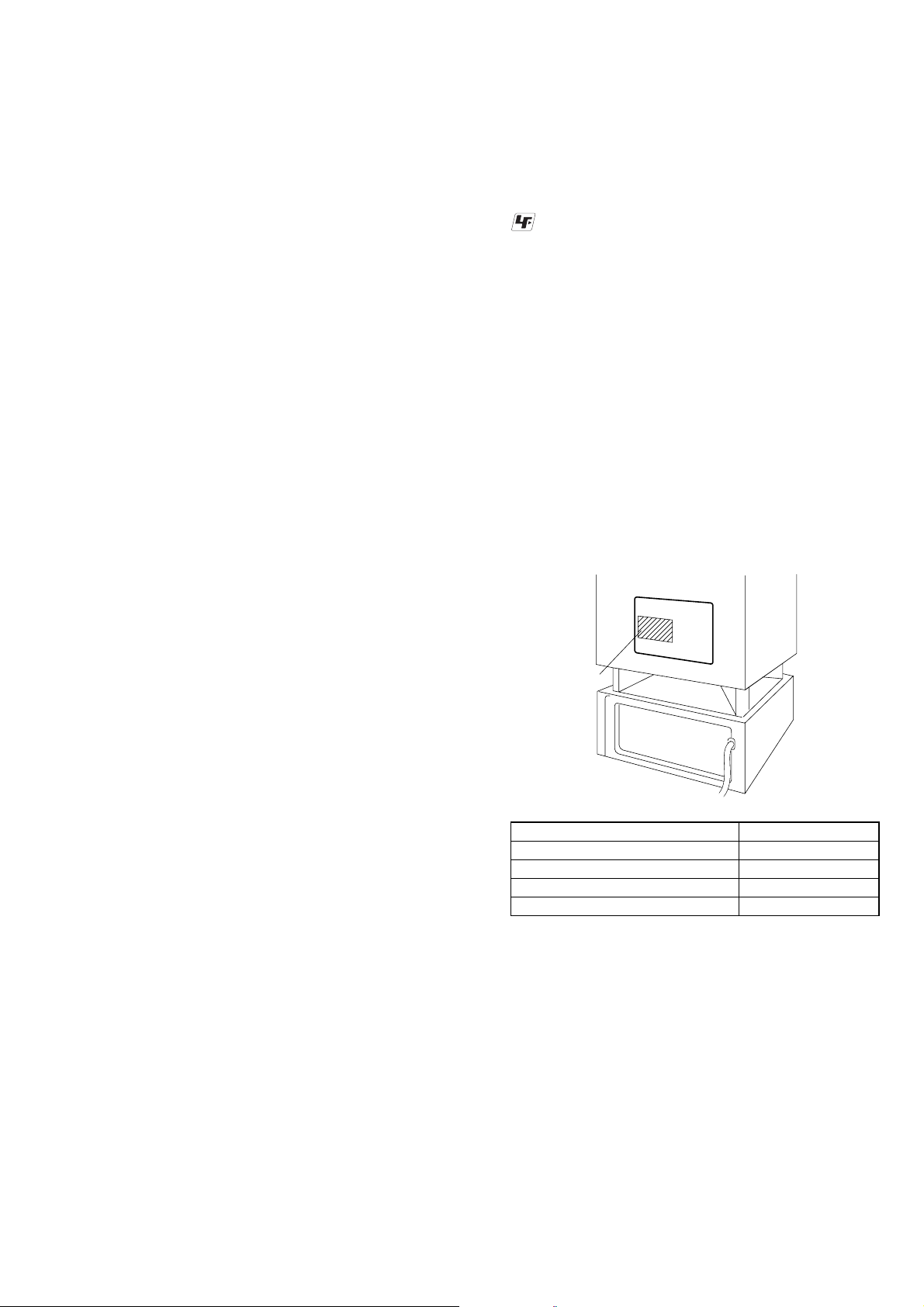
MODEL IDENTIFICATION
– Rear View –
Part No.
6. EXPLODED VIEWS
6-1. Overall Section (SA-WSLF10) ....................................... 44
6-2. AMP Assy Section (SA-WSLF10).................................. 45
6-3. MAIN Board Section (SA-WSLF10).............................. 46
6-4. SS-CTL10/TSL10/TSL11 Section .................................. 47
6-5. Stand Section ................................................................... 48
7. ELECTRICAL PARTS LIST................................ 49
MODEL PART No.
US model 2-590-864-0[]
Taiwan model 2-590-866-0[]
Singapore model 2-590-867-0[]
Australian model 2-591-603-0[]
3
SA-WSLF10/SS-CTL10/TSL10/TSL11
• The units that are required for the system operation check during repair service
Units required for
Unit.
need to
checking
Super audio CD/
DVD player : HCD-LF10
Sub woofer :
SA-WSLF10
Front speaker :
SS-TSL10
Center speaker :
SS-CTL10
Surround speaker :
SS-TSL11
Remote commander :
RM-SP320
*1 Only the defective unit. *2 Either one of them.
Units with a mark: The units that are required for the system operation check during repair service
However, there can be a case that some units of the system need to not be brought into repair shop depending on the unit. that became defective.
operation
Super audio CD/
DVD player :
check
HCD-LF10
a
a
a
a
Sub woofer :
SA-WSLF10
a
a
a
a
Front speaker :
SS-TSL10
a*1
a*2
Center
speaker :
SS-CTL10
a
Surround
speaker :
SS-TSL11
a*1
Remote
commander :
RM-SP320
a
a
a
a
a
Remote
sensor :
DIR-R4
Surround
amplifier :
TA-SB500WR
a
a
a
aaaa
IR transmitter :
DIR-T1
IR receiver :
DIR-R1
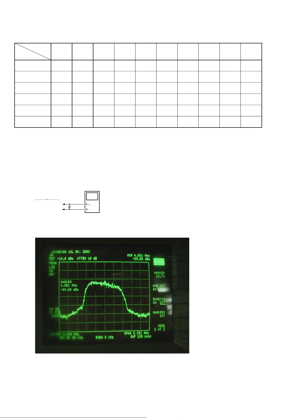
THE CHECK METHOD OF THE OUTPUT SIGNAL FROM TX BOARD
Procedure:
1. A spectrum analyzer is connected to pin 1 and pin 2 of the output connector (CN803) of TX board.
digital
voltmeter
TX board
pin
10 Ω (0.5%)
1
2
CN803 pin
2. Conf irm that it is spectrum as shown in a f igure with the spectrum analyzer . It is normal if the signal of a 3MHz to 6MHz zone (a center
is 4.5MHz) can be checked.
3. When the output signal from TX board is normal, pin 8 (SDATA), pin 4 (LRCKO) and pin 5 (BCKO) of the input signal connector
(CN801) are investigated.
4
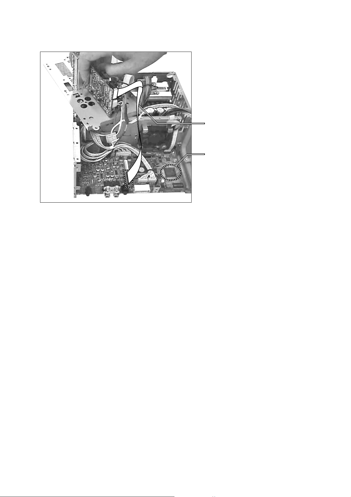
SERVICING POSITION (MAIN Board)
SA-WSLF10/SS-CTL10/TSL10/TSL11
Connect the MAIN board and the VIDEO I/O board
using the extension cable and check the MAIN board.
J-2501-245-A
(1mm/23P/L300)
IC525 on the MAIN board
CAUTION:
Keep your eyes 10 cm or more away from the infrared laser unit (DIR-T1).
Do not view directly the laser beam.
5
SA-WSLF10/SS-CTL10/TSL10/TSL11
SECTION 2
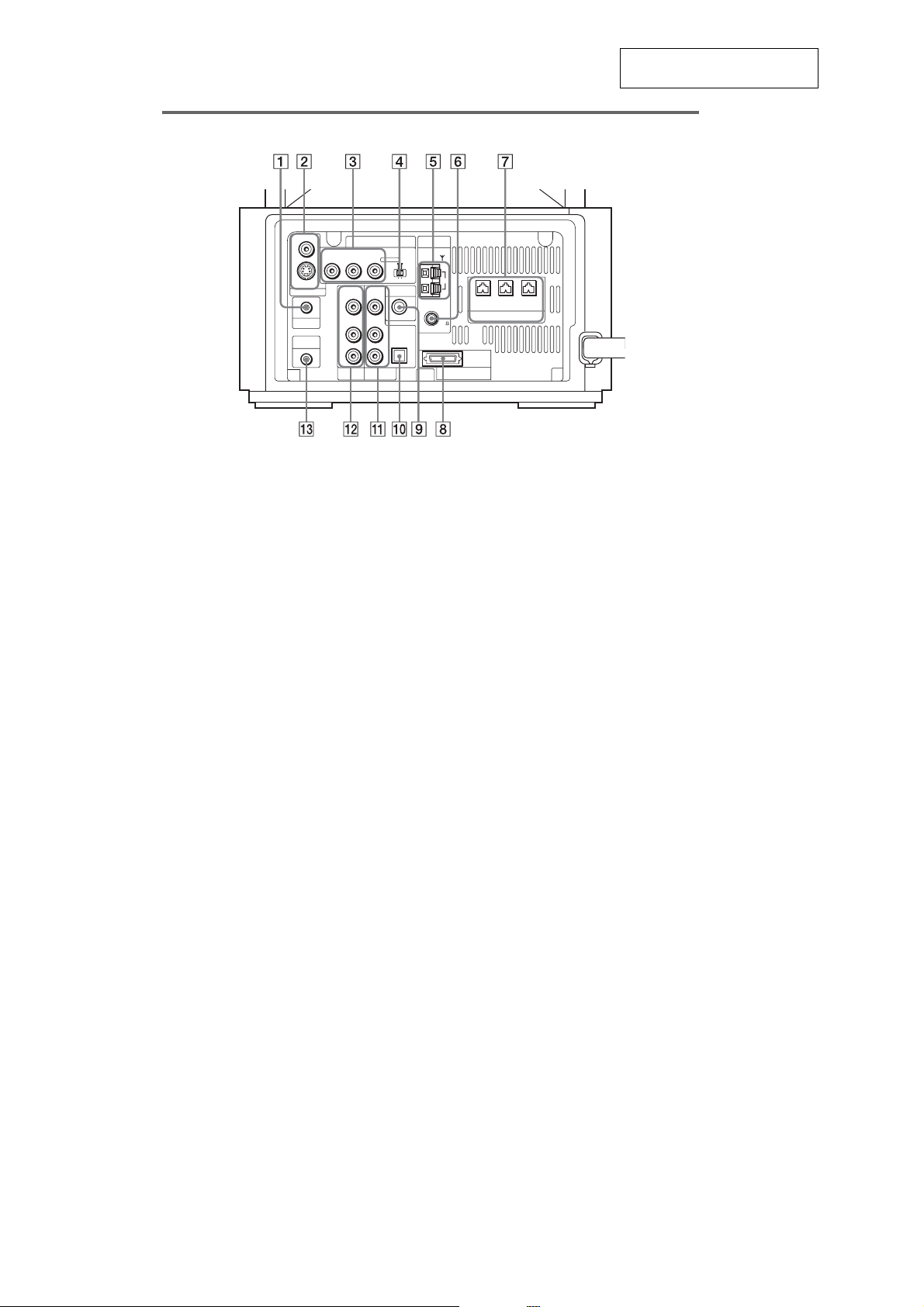
Subwoofer (Rear Panel)
GENERAL
This section is extracted from
instruction manual.
VIDEO
S VIDEO (DVD ONLY)
MONITOR OUTPUT
PHONES
DIR-R4
COMPONENT VIDEO OUT ANTENNA
PB/CBPR/CRSCAN SELECT
Y
VIDEO
VIDEO DIR-T1
IN
IN
AUDIO
AUDIO
IN
IN
OPTICAL
LL
R
VIDEO
DIGITAL IN
R
SAT
A PHONES jack
B MONITOR OUTPUT (VIDEO/S VIDEO)
jacks
C COMPONENT VIDEO OUT jacks
D COMPONENT VIDEO OUT/SCAN
SELECT switch
E AM terminals
F FM 75Ω COAXIAL jack
G SPEAKER jacks
INTERLACESELECTABLE
AM
CENTER FRONT L
FRONT R
(FOR SS-TSL10 , SS-CTL10)
FM
75
COAXIAL
SYSTEM CONNECTOR
SPEAKER
FOR HCD-LF10
H SYSTEM CONNECTOR jack
I DIR-T1 jack
J SAT OPTICAL DIGITAL IN jack
K SAT (VIDEO IN/AUDIO IN (L/R)) jacks
L VIDEO (VIDEO IN/AUDIO IN (L/R)) jacks
M DIR-R4 jack
6
SA-WSLF10/SS-CTL10/TSL10/TSL11
SECTION 3
DISASSEMBLY
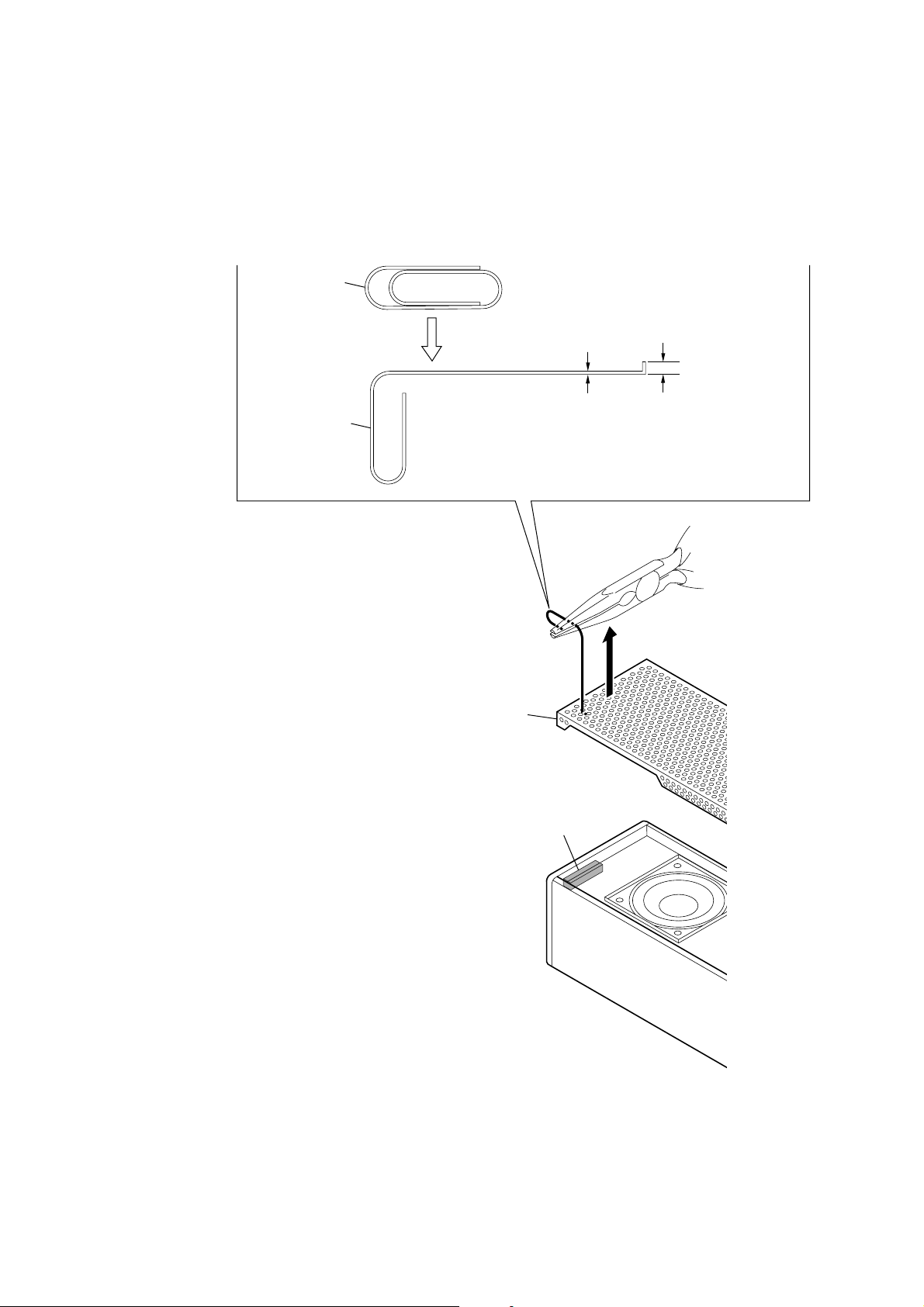
HOW TO REMOVE THE FRONT GRILLE (SS-CTL10/TSL10/TSL11)
Raise the front grille gently through the following procedure.
1
Prepare one clip (thickness φ0.8 mm).
2
Bend the leading end by about 3 mm.
3
Insert the clip into a hole in the front grille and raise the front grille.
clip
φ
0.8mm
clip
3mm
Note: The front grille has been stuck with the rubber.
(The sticking location is different depending on the speaker.)
front grille
rubber
7
SA-WSLF10/SS-CTL10/TSL10/TSL11
p
e
SECTION 4
ELECTRICAL ADJUSTMENT
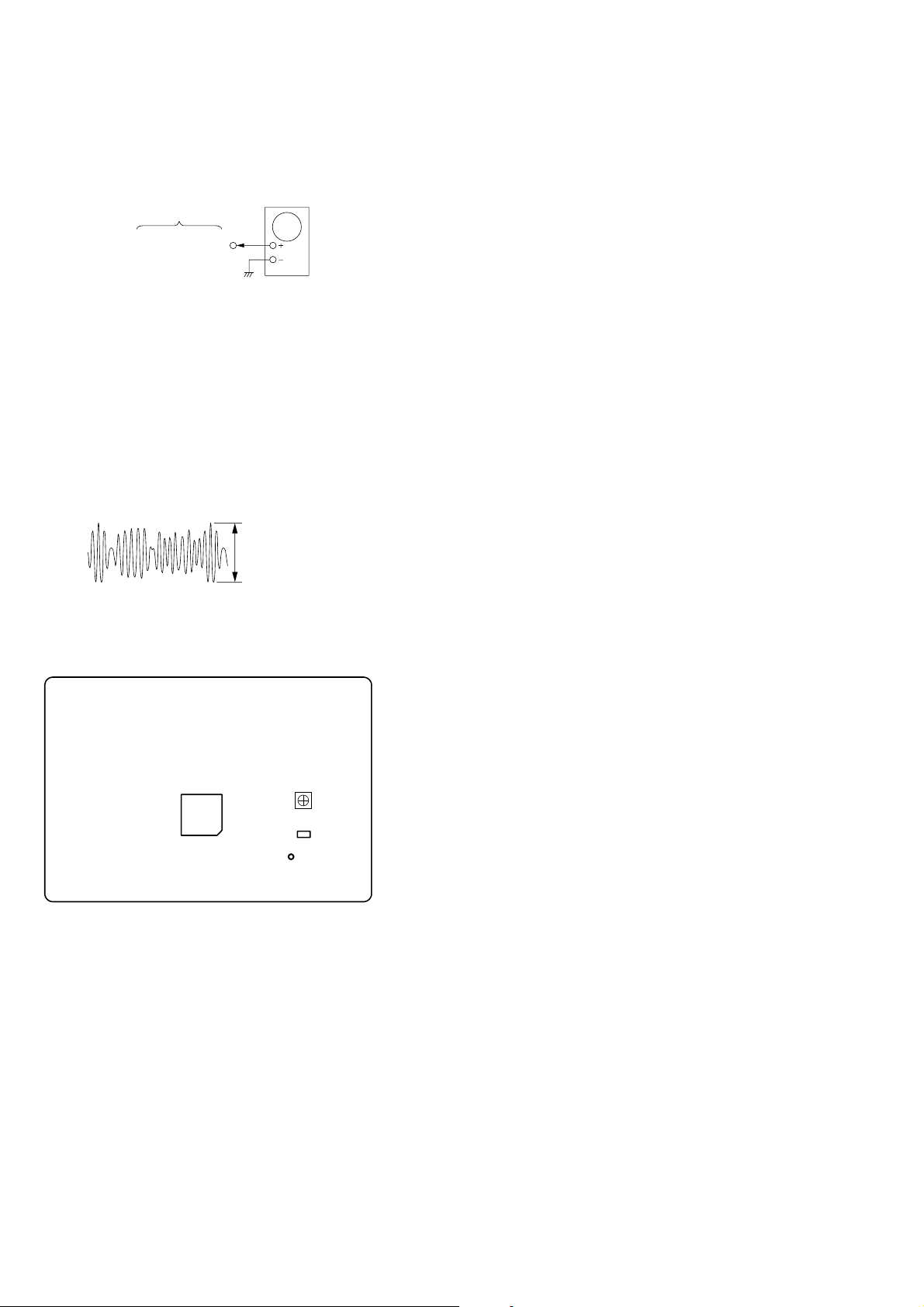
DIAT SIGNAL RF LEVEL ADJUSTMENT
This adjustment is performed in order to adjust the transmission
distance of RF signal for DIAT communication.
Connection:
TX board
TP815
(RF AMP OUT)
Procedure:
1. Connect the oscilloscope to TP815 (RF AMP OUT) and GND
on the TX board.
2. Connect DIR-T1 to DIR-T1 jack (J908).
3. Adjust RV801 on the TX board so that the center of waveform
becomes trigger level 1.05 Vp-p.
(*Trigger position: –4 DIV)
4. Confirm trigger is locked.
5. Adjust RV801 on the TX board so that the center of waveform
becomes 2.2 to 2.4 Vp-p.
oscilloscop
VOLT/DIV : 500 mV
TIME/DIV : 500 ns
level : 2.2 to 2.4 Vp-
RF Signal Reference Waveform
Adjustment Location:
– TX BOARD (Component Side) –
IC804
RV801
DIAT Signal
RF Level Adjustment
IC805
TP815
(RF AMP OUT)
8
SECTION 5
DIAGRAMS
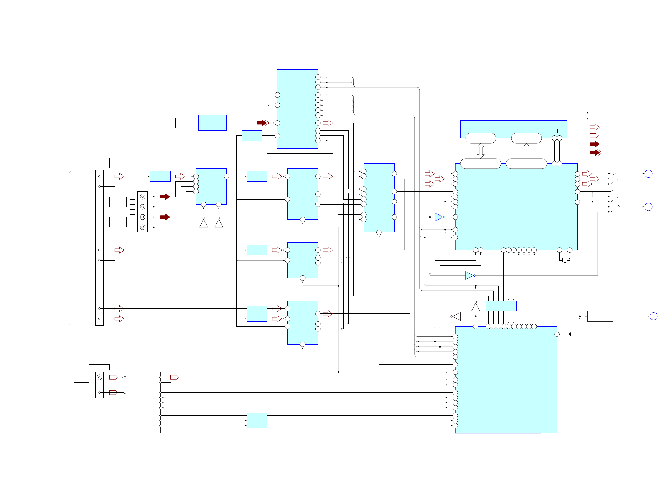
5-1. BLOCK DIAGRAM – AUDIO DSP Section –
CN502 (1/3)
SYSTEM
CONNECTOR
(FROM HCD-LF10)
FRONT-L
FRONT-R
SURROUND-L
SURROUND-R
9
10
11
12
R-CH
VIDEO
AUDIO IN
SAT
AUDIO IN
R-CH
L
R
L
R
J501
LINE AMP
IC509
R-CH
R-CH
OPTICAL
DIGITAL IN
DIGITAL OPTICAL
12 X0 13X
14 X1
15 X2
13 X3
Q504 Q503
RECEIVER
IC501
SELECTOR
IC503
A
10
SA-WSLF10/SS-CTL10/TSL10/TSL11
DIGITAL AUDIO
INTERFACE RECEIVER
IC519
24AUDIO (O)
34ERROR (O)
17XSTATE (O)
X500
24.576MHz
LEVEL SHIFT
IC514
LINE AMP
IC510
B
9
LINE AMP
IC508
22 XIN (I)
21 XOUT (O)
4DIN1 (I)
20 XMCK (O)
A/D CONVERTER
1 12LIN
15 SCKI
A/D CONVERTER
1 12LIN
15 SCKI
IC513
7
IC512
7
DOUT
LRCK
PDWN
DOUT
LRCK
PDWN
35DO (O)
36DI (I)
38CL (I)
37CE (I)
48XMODE (I)
16DATA (0)
14BCK (0)
15LRCK (0)
13CKOUT (0)
11BCK
10
11BCK
10
AUDIO
ERROR
XSTATE
DIR_DO
DIR_HDIN
DIR_HCLK
DIR_CE
DIR_XMODE
21A
31B
52A
62B
11 3A
10 3B
14 4A
13 4B
SELECTOR
IC522
/BA
1
S-RAM
IC527
D0 – D15 A0 – A15
7 – 10, 13 – 16,
29 – 32, 35 – 38
5 – 1, 44 – 42,
27 – 24, 21 – 18
WEWE0
CSCE0
17
6
R-ch is omitted due to same as L-ch.
SIGNAL PATH
: AUDIO
: TUNER
: AUX IN (AUDIO)
: DIGITAL IN
108, 107, 105 – 102,
99, 98, 80 – 77, 75 – 72
D0 – D15
HDIN33HCLK
34
IC521
IC530
18 SDI1
114 S D I 3
30 SDI2
17 BCKI1
29 BCKI2
15 LRCKI1
28 LRCKI2
22 KFSIO
69 GP8
59 EXLOCK
41Y
72Y
93Y
124Y
AUDIO
ERROR
112, 110, 109, 97 – 92,
82 – 85, 66 – 64
A0 – A15
AUDIO DIGITAL
SIGNAL PROCESSOR
IC525
HCSDSP_CS
HDOUTDSP_DO
HACNDSP_HACN
BSTDSP_BST
GP9DSP_GP9
36
35
32
56
68
113
PMDSP_PM
XRSTDSP_RESET
2
45
44
MCLK1
9
X501
13.9MHz
12
23SDO1
25SDO3
24SDO2
20BCKO
19LRCKO
MCLK2
SDO1
SDO2
SDO3
BCKO
BCKO
LRCKO
LRCKO
SCK
SDO1, SDO3,
BCKO, LRCKO, SCK
SDO2,
BCKO, LRCKO
A
(Page 10)
B
(Page 11)
CENTER
SW (LFE)
FM 75Ω
COAXIAL
AM
13
11
ANTENNA
TUNER UNIT
FM ANT
AM ANT
L-CH
R-CH
MUTE
TUNED
STEREO
A/D CONVERTER
IC511
1
LINE AMP
IC507
R-CH
DI
CK
CE
DO
LEVEL SHIFT
IC520
LIN
2RIN
15 SCKI
PDWN
7
DOUT
LRCK
12
11BCK
10
XSTATE
DIR_DO
DIR_HDIN
DIR_HCLK
DIR_CE
DIR_XMODE
Q514
Q515
25 DIR_DO
7DIG_DI
8DIG_CLK
20 DIR_CE
24 DIR_XMODE
3DIR/ADC_2
66 ADC_PDOWN
48 AV_SEL1
47 AV_SEL0
54 TUN_DO
55 TUN_CLK
53 TUN_CE
57 TU_MUTE
52 TUN_DI
51 TUNED
56 TU_STEREO
23
DIR_ANADIG
18
LEVEL SHIFT
IC524
14
6
15
19
DIR_ERR
DIR_XSTAT
IC526 (1/3)
17
22
DIR_ZERO
SYSTEM CONTROLLER
MUTIG SWITCH
Q516
16
13
12
91UNMUTE
D503
AMP_SOFT MUTE
C
(Page 10)
SA-WSLF10/SS-CTL10/TSL10/TSL11
99
SA-WSLF10/SS-CTL10/TSL10/TSL11
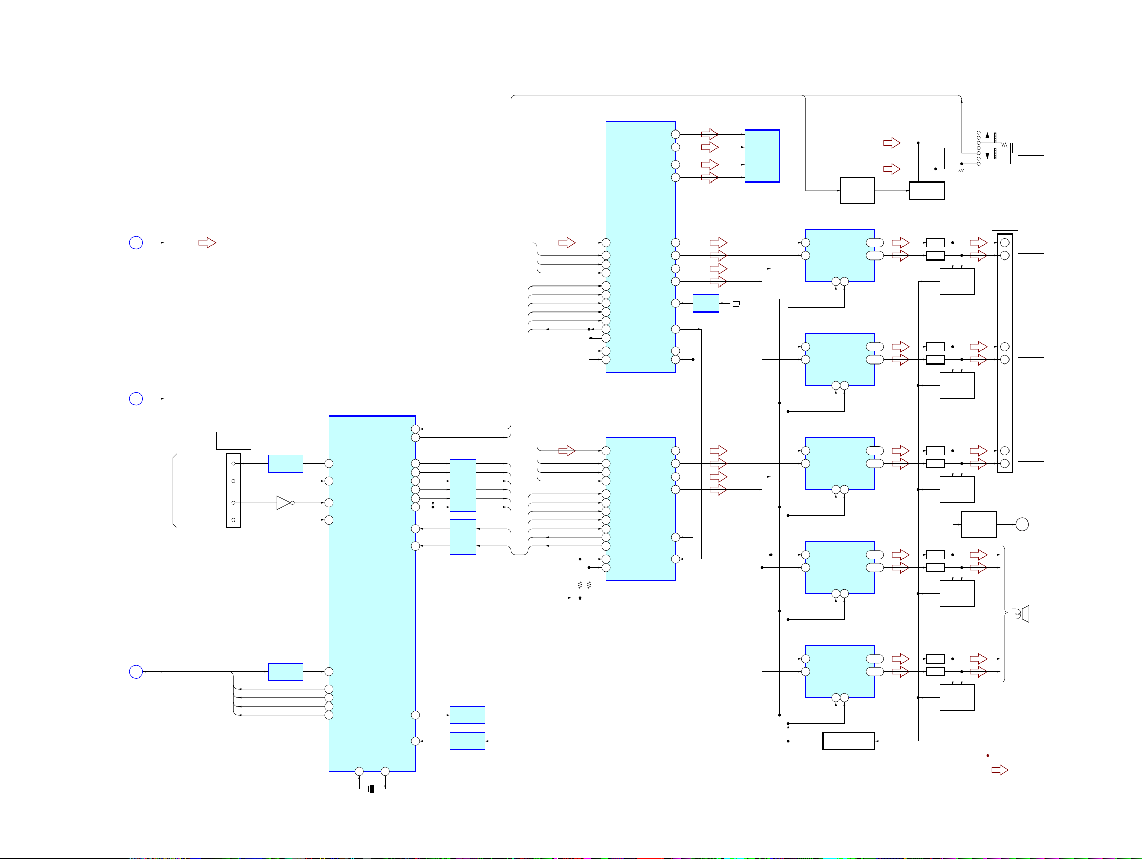
5-2. BLOCK DIAGRAM – AUDIO Section –
STREAM PROCESSOR
IC108
HPOUTL1
HPOUTL2
HPOUTR1
HPOUTR2
HPMUTE
45
43
41
39
HEADPHONE
AMP
IC301
MUTING
CONTROL
Q517
MUTING
Q903 – 906
HPSW
J903
PHONES
(Page 9)
(Page 9)
(Page 11)
SDO1, SDO3,
BCKO, LRCKO, SCKO
A
AMP_SOFTMUTE
C
(FROM HCD-LF10)
CSOD, SDATA,
SCLK, XLAT, XRST
D
UCOM-DO
UCOM-DI
CABLE_DETECT2
AMPMICOM_RESET
CN502 (2/3)
SYSTEM
CONNECTOR
19
18
20
22
CSOD
SDATA
SCLK
XLAT
XRST
LEVEL SHIFT
IC506 (1/2)
Q508
LEVEL SHIFT
IC523 (1/3)
1
DAMP_DATA
100
IF_DATA_IN
98
STOP_IN
34
RESET
SYSTEM CONTROLLER
DIAT_CSOD
95
DIAT_DO
4
DIAT_CLK
5
DIAT_CS
96
DIAT_XRST
97
DAMP_HP_MUTE
DAMP_DATA
DAMP_CLK
DAMP_CS1
DAMP_CS3
DAMP_RST
DAMP_MUTS
OVERFLOW_1
OVERFLOW_2
IC526 (2/3)
DRICE_RST
HP_SW
POWER DRIVER
IC101
SDO1
SCK
BCKO
LRCKO
SCDT
SHIFT
LATCH1
INIT
SOFTMUTE
OVF
65
60
98
99
29
31
26
28
85
86
43
LEVEL
SHIFT
IC529
(1/2)
LEVEL
SHIFT
IC523
(2/3)
LEVEL SHIFT
IC529 (2/2)
HPSW
HPMUTE
SCDT
SHIFT
LATCH1
LATCH3
INIT
SOFTMUTE
OVF
OVF2
SDO3
SCK
BCKO
LRCKO
SCDT
SHIFT
LATCH3
INIT
SOFTMUTE
OVF
OVF2
AMP +3.3V
31 DATA
36 XFSIN
30 BCK
29 LRCK
21 SCDT
22 SCSHIFT
23 SCLATCH
27 INIT
19 SOFTMUTE
25 OVF FLAGR
24 OVF FLAGL
18 NSPMUTE
20 PGMUTE
STREAM PROCESSOR
IC110
31 DATA
36 XFSIN
30 BCK
29 LRCK
21 SCDT
22 SCSHIFT
23 SCLATCH
27 INIT
19 SOFTMUTE
25 OVF FLAGR
24 OVF FLAGL
18 NSPMUTE
20 PGMUTE
OUTR1 6
OUTR2 4
OUTL1 11
OUTL2 9
XFSOIN
XFSOOUT 14
FSOCKO
FSOI
OUTR1 6
OUTR2 4
OUTL1 11
OUTL2 9
FSOI
XFSOIN 48
PWM_BP
2
PWM_AP
17
OSC
48
IC305
X450
49.152MHz
2
37
38
38
17
2
17
2
17
2
17
PWM_BP
PWM_AP
PWM_BP
PWM_AP
PWM_BP
PWM_AP
PWM_BP
PWM_AP
OUT_B
OUT_A
/SD
/RST
13
4
POWER DRIVER
IC102
OUT_B
OUT_A
/SD
/RST
13
4
POWER DRIVER
IC105
OUT_B
OUT_A
/SD
/RST
13
4
POWER DRIVER
IC106
OUT_B
OUT_A
/SD
/RST
13
4
POWER DRIVER
IC107
OUT_B
OUT_A
/SD
/RST
13
4
29, 30
25, 26
29, 30
25, 26
29, 30
25, 26
29, 30
25, 26
29, 30
25, 26
L.P.F.
L.P.F.
L.P.F.
L.P.F.
L.P.F.
L.P.F.
L.P.F.
L.P.F.
L.P.F.
L.P.F.
OVER LOAD
DETECT
Q101, 102
OVER LOAD
DETECT
Q103, 104
OVER LOAD
DETECT
Q109, 110
OVER LOAD
DETECT
Q111, 112
OVER LOAD
DETECT
Q113, 114
FAN MOTOR
Q303, 304
DRIVER
J906
SPEAKER
+
–
+
–
+
–
FRONT L
FRONT R
CENTER
M301
M
(FAN)
(SUB WOOFER)
SP901
SA-WSLF10/SS-CTL10/TSL10/TSL11
DRI_OCP
X139X2
38
X502
20MHz
44
LEVEL SHIFT
IC523 (3/3)
PROTECT DETECT
Q301
SIGNAL PATH
: AUDIO
1010
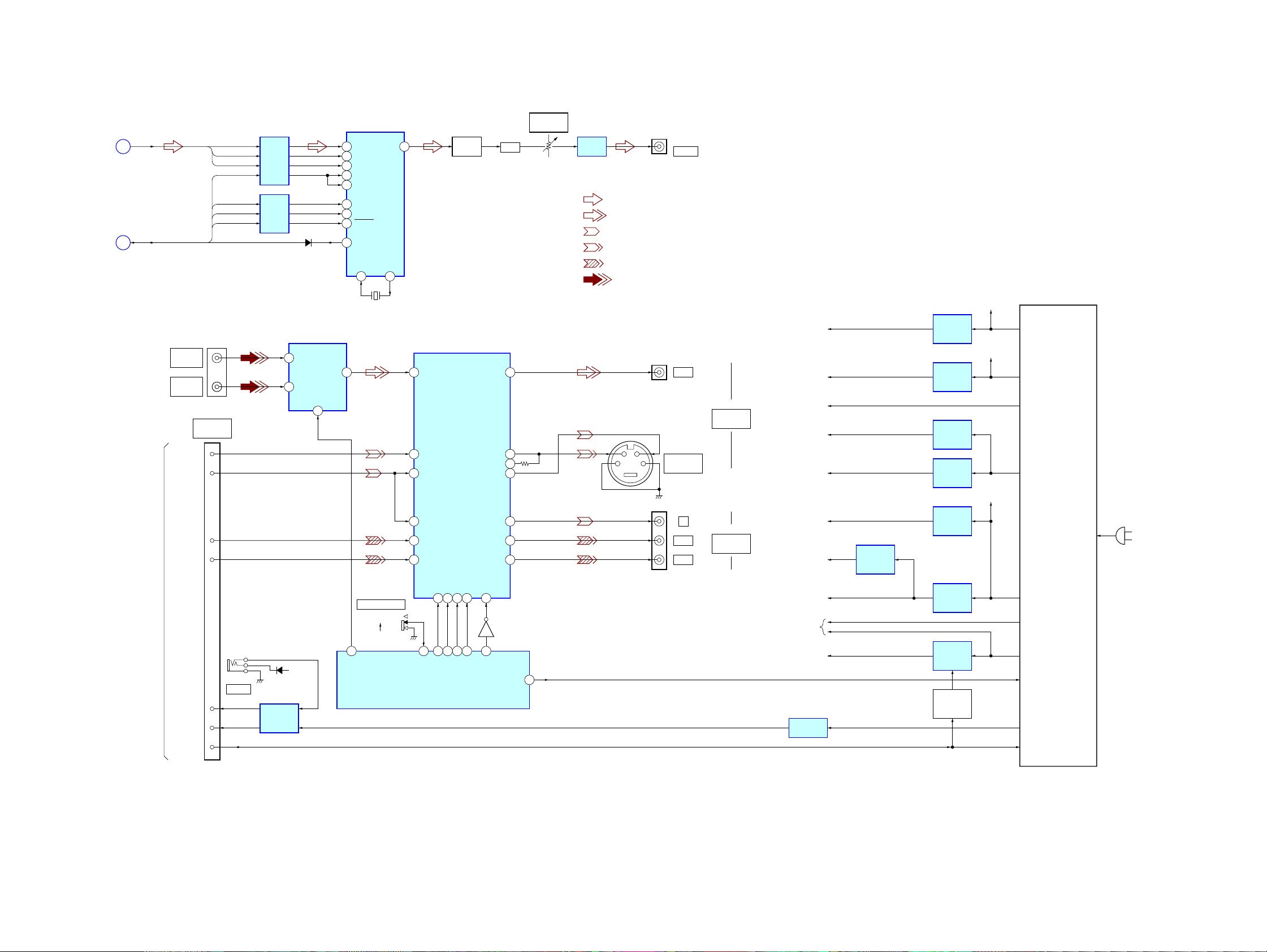
5-3. BLOCK DIAGRAM – VIDEO/POWER SUPPLY Section –
SA-WSLF10/SS-CTL10/TSL10/TSL11
(Page 9)
(Page 10)
SDO2, BCKO, LRCKO
B
CSOD, SDATA,
SCLK, XLAT, XRST
D
VIDEO
VIDEO IN
SAT
VIDEO IN
C/CVBS
CB/R
CR/R
J904
CN502 (3/3)
SYSTEM
CONNECTOR
3
1
Y/G
7
5
SDO2
BCKO
LRCKO
XRST
SDATA
SCLK
XLAT
CSOD
LEVEL
SHIFT
IC802
LEVEL
SHIFT
IC803
1
3
D800
SELECTOR
IC903
IN1
IN2
2
YOUT
SW1
RF MODULATOR,
D/A CONVERTER
IC804
48
DTIN
DAAOUT
50
BCK
49
LRCK
64
XRST
41
APS
15
SWDT
13
SCLK
14
XCSEN
16
CSOD
OSCI57OSCO
X801
24.756MHz
7
RV801
DIAT SIGNAL
RF LEVEL
21
BUFFER
Q801
L.P.F.
RF AMP
IC805
J908
DIR-T1
• SIGNAL PATH
: AUDIO
: VIDEO
: Y
: CHROMA
: COMPONENT VIDEO
59
VIDEO AMP, 75Ω DRIVER
IC902
4
2
6
10
12
14
CVBSIN
CIN
YIN
CYIN
CBIN
CRIN
CVBS OUT
C OUT
S-DCOUT
YOUT
CYOUT
CBOUT
CROUT
23
26
27
21
20
18
16
: AUX IN (VIDEO)
VIDEO
CY
S VIDEO
(DVD ONLY)
Y
PB/CB
PR/CR
J907
MONITOR
OUTPUT
J909
COMPONENT
VIDEO OUT
+1.8V
+2.6V
+5V
+5V
+9V
+2.5V
+2.5V
REGULATOR
IC801
+1.8V
REGULATOR
IC303
+2.6V
REGULATOR
IC528
+5V
REGULATOR
IC515
+5V
REGULATOR
IC516
+9V
REGULATOR
IC517
AMP +3.3V
+3.3V
+12V
3.3V
3.3V
E5.6V+5.6V
6.2V
SWITCHING
REGULATOR
(AC IN)
(FROM HCD-LF10)
SIRCS
AC-DETECT
P. CONT1
MUTE1
70
50
IP_SW
3
13
61
AV_SEL3
MUTE25YC-MIX25S1
69
AV_SEL4
S901
SCAN SELECT
INTERLACE
SELECTABLE
72
J502
DIR-T4
23
16
17
D502
LEVEL SHIFT
IC506 (2/2)
+5.6V
AV_SEL5
IC526 (3/3)
SYSTEM CONTROLLER
62
YC-MIX
VS/WIDE
I/P
9
63
I/P_SEL
Q913
P-PWM
+9V
POWER DRIVER
B+
+15V
11
DETECTOR
IC531
+9V
REGULATOR
IC518
+15V
REGULATOR
IC800
REGULATOR
CONTROL
Q506, 801
12V
12V
18V – 30V
V-CONT
AC-DET
ON/OFF
(STANDBY/POWER)
SA-WSLF10/SS-CTL10/TSL10/TSL11
1111
SA-WSLF10/SS-CTL10/TSL10/TSL11
d
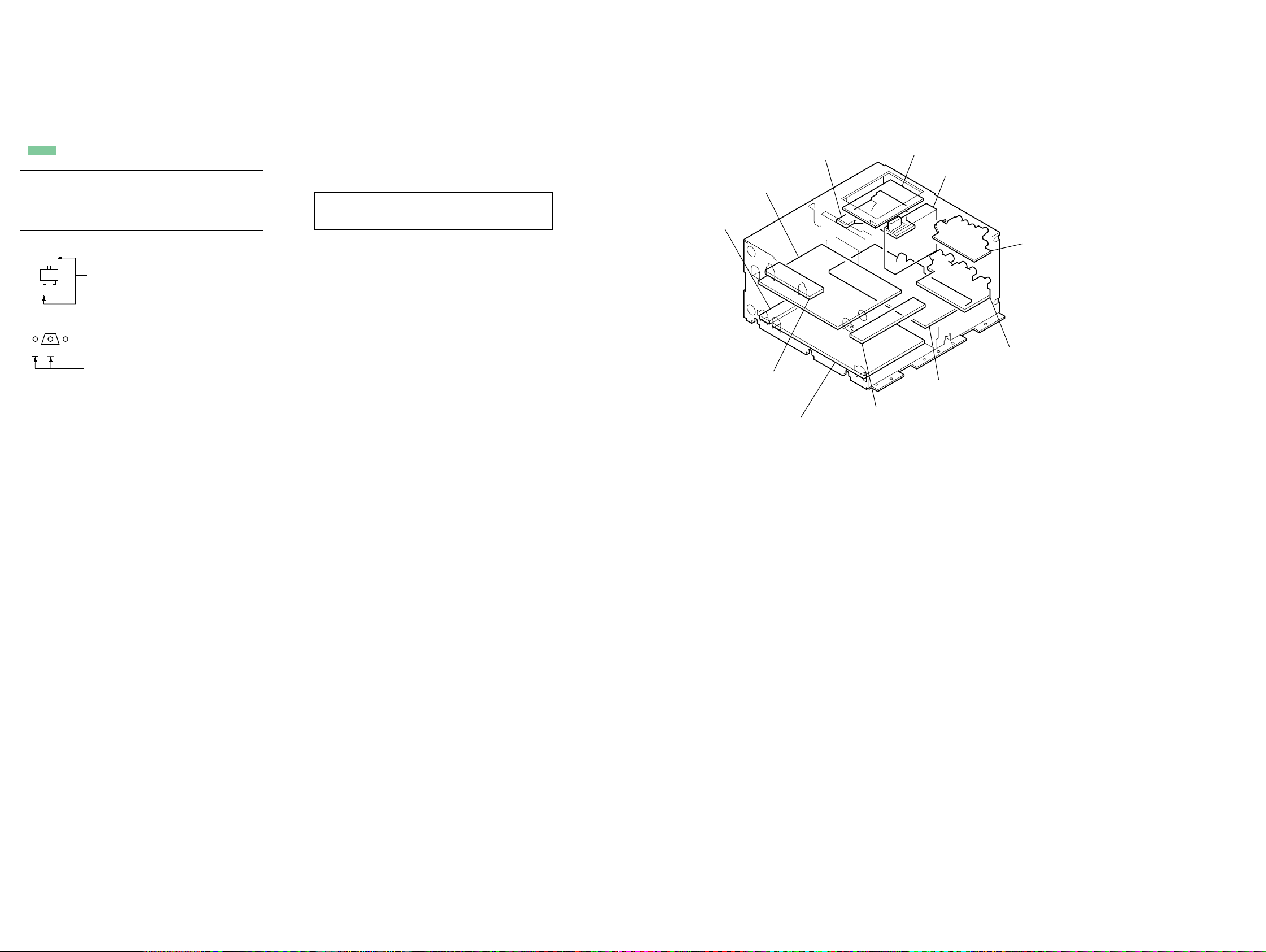
• Note for Printed Wiring Boards and Schematic Diagrams
Note on Printed Wiring Board:
• X : parts extracted from the component side.
• Y : parts extracted from the conductor side.
f
•
• : Pattern from the side which enables seeing.
(The other layers' patterns are not indicated.)
Caution:
Pattern face side: Parts on the pattern face side seen from
(Conductor Side) the pattern face are indicated.
Parts face side: Parts on the parts face side seen from
(Component Side) the parts face are indicated.
• Indication of transistor
: internal component.
C
Q
B
E
Q
B
CE
These are omitted.
These are omitted.
Note on Schematic Diagram:
• All capacitors are in µF unless otherwise noted. (p: pF)
50 WV or less are not indicated except for electrolytics
and tantalums.
• All resistors are in Ω and 1/
specified.
• f : internal component.
• C : panel designation.
Note: The components identified by mark 0 or dotted line
with mark 0 are critical for safety.
Replace only with part number specified.
• A : B+ Line.
• H : adjustment for repair.
• Voltages and waveforms are dc with respect to ground
under no-signal (detuned) conditions.
no mark : DVD PLAY
(): TUNER (FM/AM)
• Voltages are taken with a V OM (Input impedance 10 MΩ).
Voltage var iations may be noted due to normal production tolerances.
• Waveforms are taken with a oscilloscope.
Voltage var iations may be noted due to normal production tolerances.
• Circled numbers refer to waveforms.
• Signal path.
F : AUDIO
L : VIDEO
E : Y
a : CHROMA
r : COMPONENT VIDEO
f : AUX IN (AUDIO)
h : DIGITAL IN
i : AUX IN (VIDEO)
• Abbreviation
AUS: Australian model
SP : Singapore model
TW : Taiwan model
4
W or less unless otherwise
• Circuit Boards Location
S-MASTER board
PLF board
15V-RELAY board
SPK-OUT board
SWITCHING REGULATOR
TX board
TUNER UNIT
COMPONENT boar
VIDEO I/O board
MAIN board
15V-REG board
SA-WSLF10/SS-CTL10/TSL10/TSL11
1212
SA-WSLF10/SS-CTL10/TSL10/TSL11
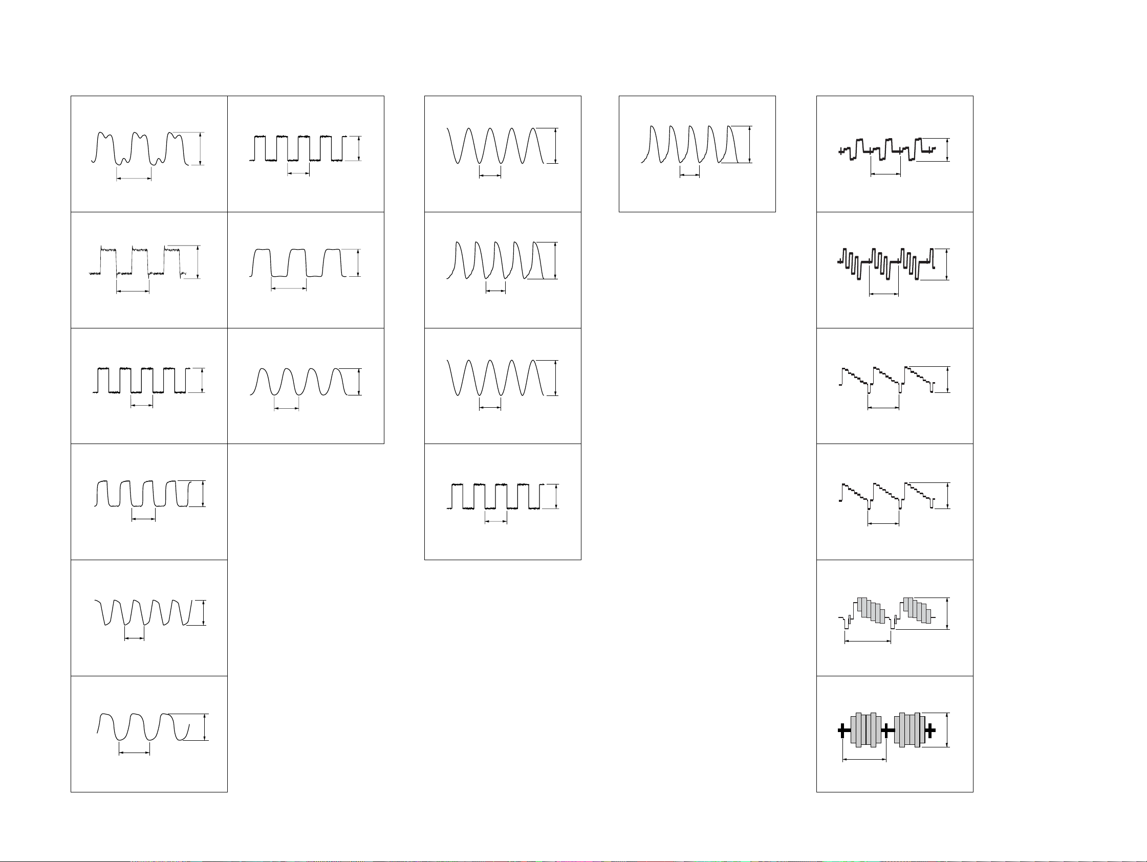
• Waveform
– MAIN Board – – S-MASTER Board – – VIDEO I/O Board –
IC519 qd (CKOUT (O))
1
IC525 ql (LRCKO)
7
qa
IC305 2
– TX Board –
IC804 tl (OSCO)
wa
IC902 qh (CROUT)
ea
(DVD play mode)
40.6 ns
2 V/DIV, 10 ns/DIV
IC519 qf (BCK (O))
2
163 ns
2 V/DIV, 50 ns/DIV
IC519 qg (LRCK (O))
3
10.4 µs
2 V/DIV, 5 µs/DIV
IC519 w; (XMCK (O))
4
3.8 Vp-p
3.8 Vp-p
3.7 Vp-p
IC525 w; (BCKO)
8
IC526 ek (X2)
9
20.8 µs
2 V/DIV, 10 µs/DIV
326 ns
2 V/DIV, 100 ns/DIV
50 ns
1 V/DIV, 20 ns/DIV
3.6 Vp-p
3.5 Vp-p
1.9 Vp-p
20.4 ns
500 mV/DIV, 10 ns/DIV
IC305 4
qs
20.4 ns
1 V/DIV, 10 ns/DIV
IC108 qf (XFSOOUT)
qd
20.4 ns
1 V/DIV, 10 ns/DIV
IC108 ej (FSOCKO)
qf
1.6 Vp-p
3.8 Vp-p
3.2 Vp-p
40.6 ns
1 V/DIV, 20 ns/DIV
2.8 Vp-p
500 mV/DIV, 20 µs/DIV
IC902 qk (CBOUT)
es
(DVD play mode)
500 mV/DIV, 20 µs/DIV
IC902 w; (CYOUT)
ed
(DVD play mode)
500 mV/DIV, 20 µs/DIV
IC902 wa (YOUT)
ef
(DVD play mode)
H
1.4 Vp-p
1.4 Vp-p
H
2.1 Vp-p
H
2 V/DIV, 50 ns/DIV
IC519 wa (XOUT (O))
5
40.8 ns
2 V/DIV, 20 ns/DIV
IC525 qs (MCLK2)
6
72.2 ns
2 V/DIV, 20 ns/DIV
81 ns
3.4 Vp-p
3.8 Vp-p
3.4Vp-p
20.8 µs
2 V/DIV, 10 µs/DIV
3.8 Vp-p
500 mV/DIV, 20 µs/DIV
IC902 wd (CVBS)
eg
(DVD play mode)
500 mV/DIV, 10 µs/DIV
IC902 wh (COUT)
eh
(DVD play mode)
H
500 mV/DIV, 10 µs/DIV
2.1 Vp-p
H
2.4 Vp-p
H
1.6 Vp-p
SA-WSLF10/SS-CTL10/TSL10/TSL11
1313
SA-WSLF10/SS-CTL10/TSL10/TSL11
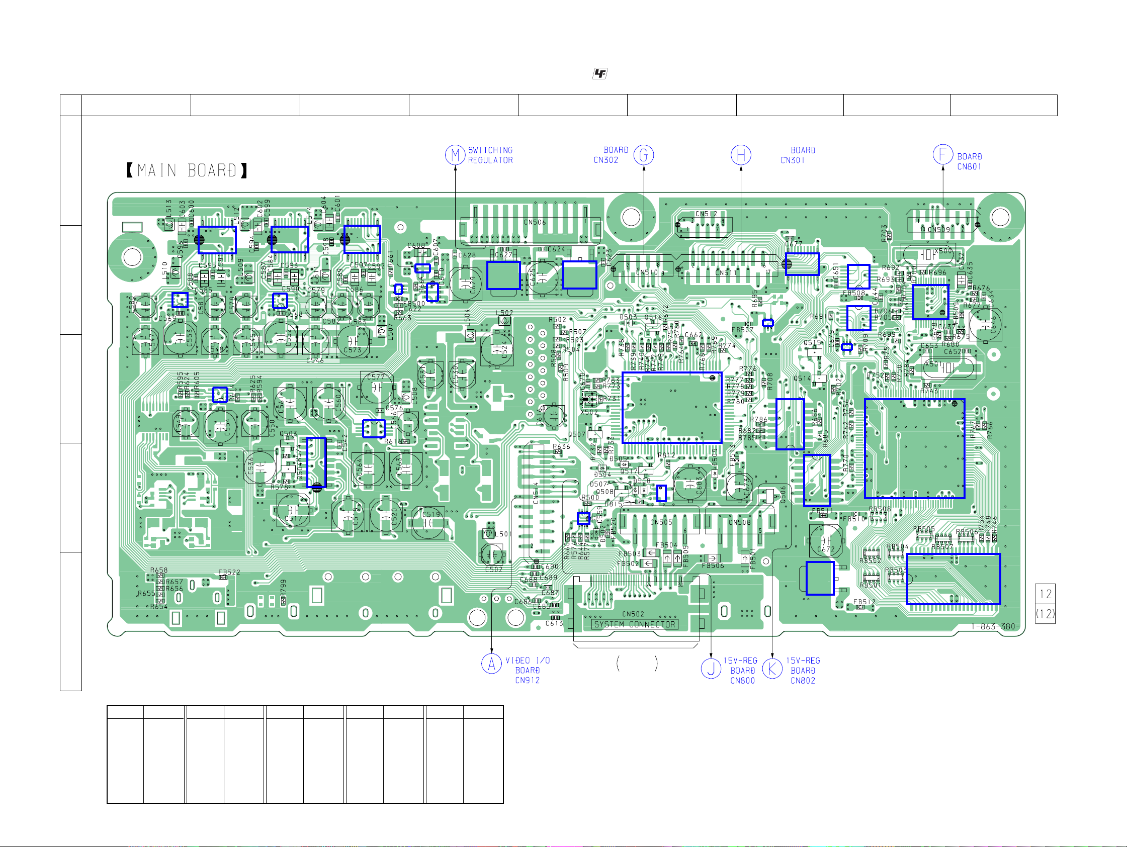
5-4. PRINTED WIRING BOARD – MAIN Board (Component Side) –
A
12
(COMPONENT SIDE)
IC512
20
1
11
10
IC511
20
1
11
10
34567
IC513
20
11
1
10
B
C
IC508
5
8
4
1
IC509
4
5
8
1
4
5
8
1
IC507
E
E
IC503
9
16
1
8
1
45
IC510
D
• See page 12 for Circuit Boards Location. : Uses unleaded solder.
S-MASTER S-MASTER
(Page 32)
(Page 21)
IC515
5
1
4
3
5
1
IC514
4
3
1
6
3
4
IC516
3
2
IC518
1
13
2
IC517
E
30
31
EXCEPT
AEP,UK,RU
IC526
8
E
50
21
20
1
4
51
E
IC531
5
E
1
3
4
IC506
58
(FOR CHECK)
1
100
8 9
TX
(Page 21)
1120
IC523
87
1
10
IC529
IC522
4
5
3
1
IC521
7
8
81
80
14
IC520
1
1
E
IC530
E
14
14
1
89
1
3
45
31
1
16
30
24
25
37
36
IC519
IC525
E
7
IC524
8
60
61
13
48
(Page 26)
12
1
1
90
120
91
E
• Semiconductor Location
Ref. No. LocationRef. No. Location
D502 D-5
D503 B-6
D504 D-5
D505 D-5
D507 D-6
D508 D-6
D509 D-6
IC503 D-3
SA-WSLF10/SS-CTL10/TSL10/TSL11
IC506 D-5
IC507 B-2
IC508 B-1
IC509 C-2
IC510 C-3
IC511 B-2
IC512 B-2
IC513 B-3
IC514 B-3
Ref. No. Location Ref. No. Location Ref. No. Location
IC515 B-4
IC516 B-4
IC517 B-5
IC518 B-4
IC519 B-8
IC520 C-7
IC521 B-7
IC522 B-8
IC523 B-8
IC524 D-7
IC525 D-8
IC526 C-6
IC527 E-9
IC528 E-7
IC529 B-7
IC530 C-8
IC531 D-6
Q503 C-2
Q504 D-3
Q506 D-7
Q507 C-5
Q508 D-5
Q514 C-7
Q515 C-7
Q516 B-6
Q517 D-6
(Page 28)
3
2
1
44 23
IC527
122
IC528
TO
HCD-LF10
(Page 32) (Page 32)
1414
SA-WSLF10/SS-CTL10/TSL10/TSL11
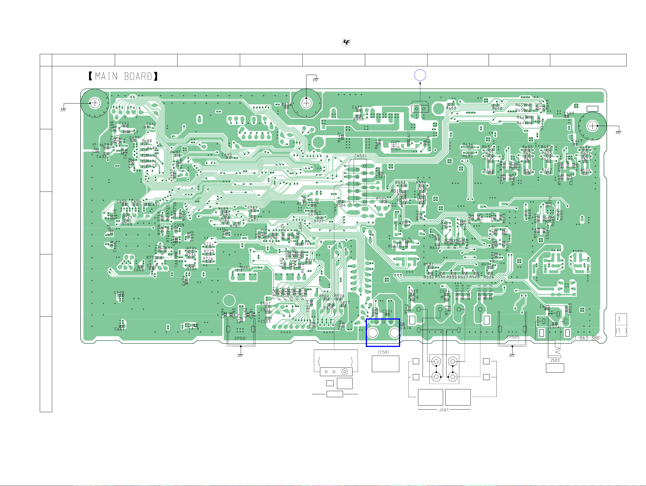
5-5. PRINTED WIRING BOARD – MAIN Board (Conductor Side) –
12
34567
(CONDUCTOR SIDE)
A
(CHASSIS)
B
• See page 12 for Circuit Boards Location. : Uses unleaded solder.
(CHASSIS)
CN507
1
2
10
11
TX
BOARD
P
CN802
12
8 9
(Page 26)
(CHASSIS)
C
D
E
13
IC501
TUNER UNIT
(CHASSIS) (CHASSIS)
SUPPLIED WITH THE
ASSEMBLED BLOCK
FM 75Ω
AM
COAXIAL
ANTENNA
OPTICAL
DIGITAL IN
L
R
AUDIO IN
SAT
L
R
VIDEO
AUDIO IN
2
2
DIR-T4
SA-WSLF10/SS-CTL10/TSL10/TSL11
1515
SA-WSLF10/SS-CTL10/TSL10/TSL11
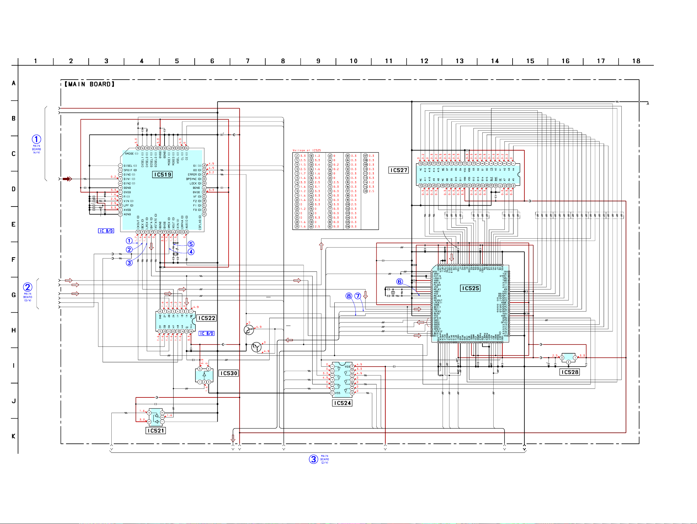
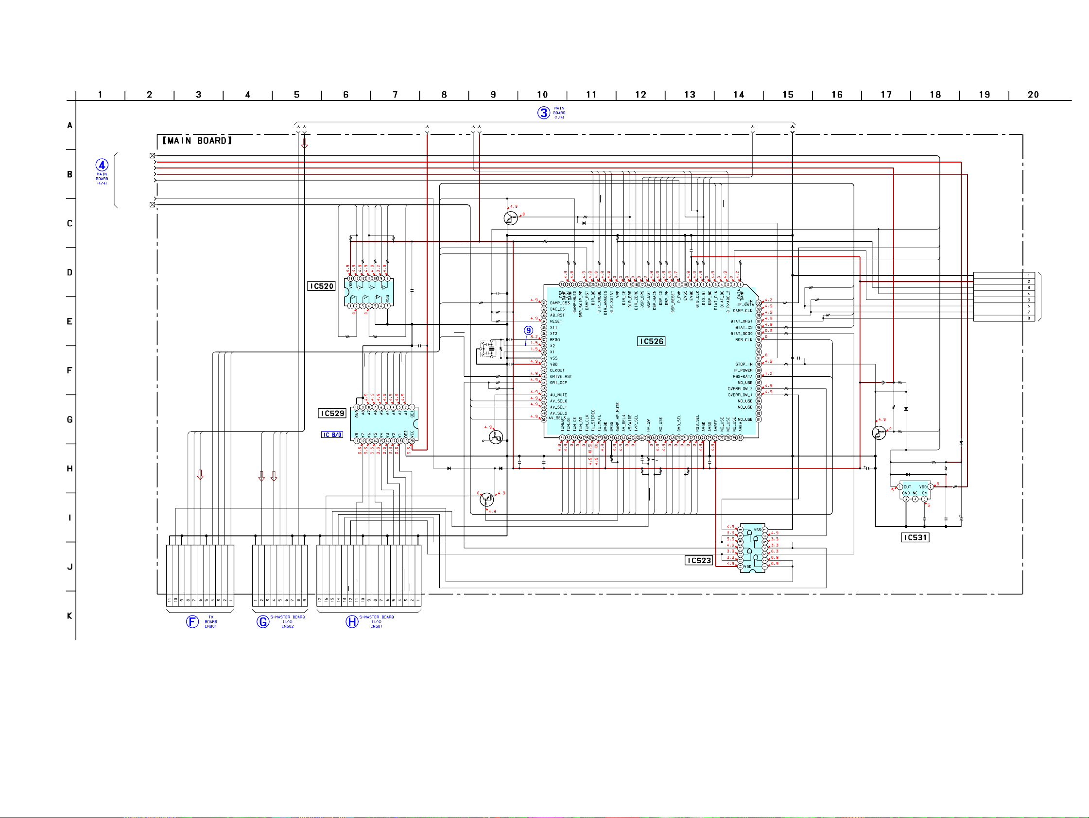
5-6. SCHEMATIC DIAGRAM – MAIN Board (1/4) –
(1/4)
D3.3V
DGND
R678
C637
4.7k
0.01
(Page 19)
R675
100
R677
R674 C632
100 10
5.6k
R692
R703
47
R704 R693
47
R695
68
1
C636
0.01
0.01
C633
33k
R673
0.1
C634
4.7k
R676
0.01
C635
0.1
C630
0.1
C631
1k
100
R679
R681
DIGITAL AUDIO
INTERFACE RECEIVER
100
100
100
R683
R684
R688
R690
FB507
V
LEVEL SHIFT
IC521
SN74LVC1G125DCKR
(Page
18)
OPT IN
C/SW_DATA
SL/SR_DATA
FL/FR_DATA
ADBCK
ADLRCK
AD_MCK
• See page 13 for Waveforms. • See page 34 for IC Block Diagrams. • See page 38 for IC Pin Function Description.
DIR_XMODE
DIR_HCLK
Q514,515
INVERTER
Q514
DTC124EKA-
T146
Q515
DTC124EKA-
T146
DIR_HDIN
DIR/ADC_2
DIR_CE
DIR_DO
DIR/ADC
DIR_ERR
DIR_XSTATE
DIR_ZERO
4
S-RAM
IC527
IS61LV6416-10TLT
RB506
100
100
100
100
C663
R746
R748
R754
0.1
DSP_PM
C657
DSP_XRST
C653
12p
LRCKO
BCKO
SDO1(FL/FR)
SDO2(SL/SR)
SDO3(FC/SW)
R724
100
R725
100
R726
100
LEVEL SHIFT
IC524
TC74HCT7007AF
(EL)
R735
100
R736
100
R734
100
DSP_HACN
DSP_HDOUT
DSP_GP9
R766
4.7k
0.1
C656
R747
R749
4.7k
C652
12p
R784
X501
680
13.9MHz
R750
100
R751
100
R752
100
C650
5
0.1
10k
C655
0.1
R743
1M
0.1
R767
C658
10k
0.1
R758
10k
DSP_HDIN
IC519
LC89056W-E
100
C645
0.1
G
C638R680
0.110k
R696
1M
R707
270
24.576MHz
0.1
R700
C642
3.3k
5p
R702
R699
R691
SELECTOR
IC522
SN74LV157APWR
C644
0.1
C679
0.1
V
GNC
IC530
MC74VHC1GU04DFT1
R698
100
R697
100
C641
7p
X500
C639
FB509
C646
220
4V
R705
100
R706
3.3k
C647
0.1
1k
100
100
FB508
R709
22
INVERTER
3
2
C659
0.1
R762R756
100100
R765
10k
R759R757 R763
4.7k4.7k 4.7k
DSP_HCLK
C661
0.01
AUDIO DIGITAL
SIGNAL PROCESSOR
CXD9720BQ
(OPEN_OK)
R761
10k
DSP_CS
C615
0
(CHASSIS)
FB512
C660
0.01
RB504
RB505
RB507
100
C666
0.1
IC525
(OPEN_OK)
(OPEN_OK)
(OPEN_OK)
C664
0.1
C667
0.1
R772
R770
10k
10k
R771
4.7k
DSP_BST
6
100
100
C668
C669
0.1
FB511
FB510
7
100
100
RB503
RB502
0.1
R775
100
IC528
NJM2391DL1-26
(TE1)
OI
G
C674
C672 C676
0.1
220
4V
+2.6V REGULATOR
100
100
RB501
RB508
0.1
SA-WSLF10/SS-CTL10/TSL10/TSL11
(Page 17)
1616
SA-WSLF10/SS-CTL10/TSL10/TSL11
5-7. SCHEMATIC DIAGRAM – MAIN Board (2/4) –
(2/4)
PANEL_IF
E5.6V
D5V
AC_DET
V_CONT
(Page 19)
ANALOG_CONT
PCONT1
T
T
A
T
A
LK
S
L
A
C
R
X
_
X
_
T
_D
_
T
T
T
IA
IA
IA
D
IA
D
D
D
)
O
O
R
K
K
C
C
/S
L
B
R
L
2(S
0
D
S
)
)
O
O
W
K
K
/FR
C
C
/S
L
B
R
L
(F
(FC
1
3
0
0
D
D
S
S
• See page 13 for Waveforms. • See page 34 for IC Block Diagrams. • See page 38 for IC Pin Function Description.
(Page 16)
1
2
LEVEL SHIFT
TC74HCT7007AF
IC520
(EL)
LEVEL SHIFT
IC529
SN74LV541APWR
5
K
L
C
_
S
D
R
R785
10k
R685 R686
100 100
5
5
3
3
EO
R
E
T
S
_
U
T
I5
I3
O
D
D
D
ED
E
E
_
_
N
R
N
U
U
TU
TU
TE
T
T
S
_
_
_
R786
U
U
T
TU
T
0
0
1
2
8
6
R
10k
00
1
7
8
6
R
R689
100
3
1
E
K
A
ET
S
E
R
_
P
M
A
D
T
T
L
S
S
A
U
C
C
C
_
_
_
D
_
M
P
P
P
P
M
M
M
FT
M
A
A
A
O
A
D
D
D
S
D
_
P
M
A
3
AMP_SOFT MUTE
5
A
T
A
D
_
S
D
R
DAMP_INIT
DAMP_CS1
C640
0.1
DAMP_CS3
DAMP_RESET
C677
0.1
IT
IN
_
P
M
A
D
D504
1SS388
4
5
DTC124EKA-
MUTING
SWITCH
R730
100
R783
10k
R773
100
X502 R731
20MHz 15k
R732
R733
AVSEL0
AVSEL1
AVSEL3
Q507
DTC144EKA-T146
NOT USED
Q517
DTA114EKA-
T146
MUTING
CONTROL
6
E
E
C
O
T
D
D
D
A
_
O
T
/A
M
S
IR
IR
X
X
D
D
_
_
IR
IR
D
D
Q516
T146
C670
0.001
1
8
4
6
C
C649
R727
0.01
100
1k
10k
D505
1SS388
R740
NO_USE
C654C651
0.010.1
1SS355TE-17
R672
10k
D503
10k
R738
100
5
D
E
N
I5
U
T
D
_
_
U
U
T
T
0
0
1
1
4
7
R
R739
100
R744
4.7k
5
O
E
E
R
T
K
E
U
O
E
L
T
D
C
C
M
S
_
_
_
_
_
U
U
U
U
U
T
T
T
T
T
9
E
O
R
P
C
R
R
_
G
E
E
_
Z
_
IR
_
P
D
IR
S
IR
D
D
D
k
0
0
1
0
1
2
4
5
7
4
R
7
R
SYSTEM CONTROLLER
µPD70F3033BYGF-
C684
0.1
R808
10k
E
L
4
ID
E
L
E
S
/W
_
S
S
V
A
V
I/P
T
S
B
_
P
S
D
0
0
1
5
5
7
R
IC526
M68-3BA-A
E
S
U
_
O
N
T
S
N
M
S
C
C
P
_
R
A
_
P
X
H
P
_
S
_
S
P
D
P
D
S
S
D
D
0
0
0
0
1
1
0
4
6
6
7
7
R
R
N
W
E
O
N
D
E
_
IX
P
T
_
M
U
C
-
O
D
C
V
A
Y
R809
1k
R812
10k
N
E
W
L
N
E
D
E
IX
S
_
P
_
T
_
M
D
U
C
_
V
O
C
D
D
V
Y
A
T
K
K
IN
L
L
D
C
C
H
H
H
_
_
_
P
IR
IR
S
D
D
D
7
1
4
.0
8
0
6
7
2
R
6
6
C
5
W
L
S
E
_
S
V
IP
A
k
0
1
1
1
8
R
L
E
5
S
L
W
_
E
S
B
S
_
G
V
R
IP
A
2
K
A
IN
_
T
L
U
D
A
C
C
O
H
_
D
D
D
_
T
_
H
/A
T
P
IA
_
S
IR
IA
P
D
D
D
D
S
D
7
4
9
6
7
R
C665
0.01
IN
P
2
DAMP_DATA
NO_USE
NO_USE
UNMUTE
NO_USE
R774
47
7
AMPMICOM_RESET
IF_DATA_IN
AMPUCOM_DATA
R776
100
DAMP_CLK
R777
C671
0.1
R779
R780
100
R778
100
100
100
RDS_CLK5
RDS_DATA5
DAMP_DATA
DIAT_XRST
DIAT_XLAT
R815
FB513
10k
R816
10k
DTC144EKA-
INVERTER
C673
47
6.3V
D507
1SS355TE-17
R817
CABLE_DET2
1k
(AMP_MICOM)
Q508
T146
AC_DET/CABLE_DET
D508 R801 R802
1SS355TE-17 10k 10k
7
1
E
9
T
0
5
5
5
D
3
S
S
1
R803
10k
C683
C682C681
100
0.10.22
10V
R708
1k
R787
47k
R781
1k
R782
1k
CN512
8P
GND
VDD
VPP
RESET
2PIN
CLK
OUT
(FOR CHECK)
IN
D
D
D
N
N
O
G
G
-
-
S
D
D
C
SA-WSLF10/SS-CTL10/TSL10/TSL11
)
R
/S
O
L
O
K
S
K
C
(
2
C
R
B
L
D
(Page 27)
DETECTOR
IC531
PST3645NR
)
C
N
(
D
N
-G
D
CN510
A
T
A
D
S
9P
T
K
T
L
A
C
L
S
X
D
S
N
CN509
R
G
11P
X
D
O
D
O
K
N
K
C
1
2
3
G
C
R
D
D
D
B
L
D
(Page 22)
E
T
U
D
D
W
N
N
S
M
K
G
G
P
P
C
D
S
D
H
H
D
T
2
F
V
O
3
2
N
F
S
T
T
V
G
E
D
A
A
O
D
R
S
L
L
(Page 22)
E
T
U
M
T
D
1
N
T
G
A
D
L
D
T
T
N
F
IF
D
IT
CN511
G
O
C
H
S
17P
IN
S
S
D
LEVEL SHIFT
IC523
TC74VHCT08AFT
(EL)
1717
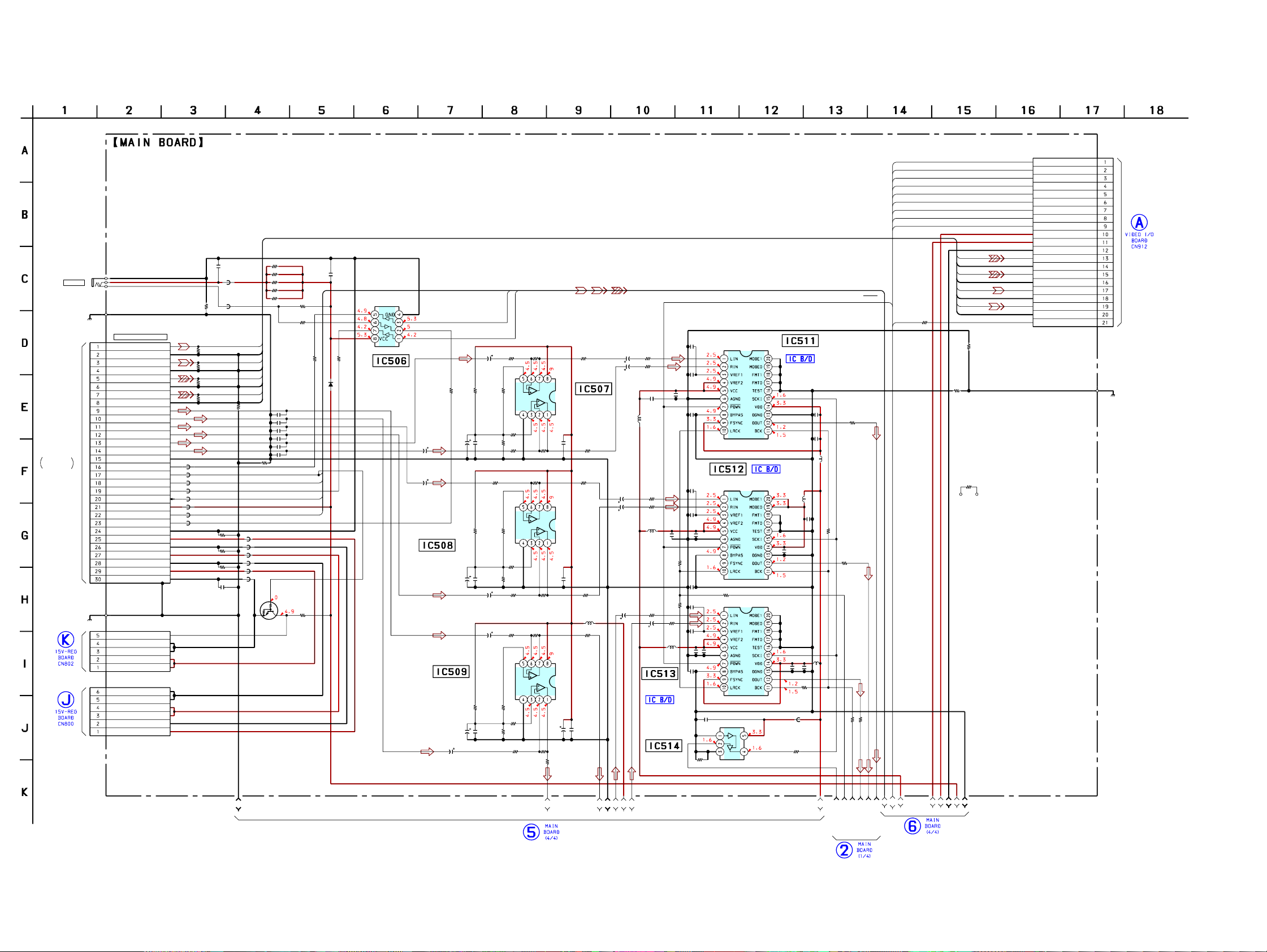
SA-WSLF10/SS-CTL10/TSL10/TSL11
5-8. SCHEMATIC DIAGRAM – MAIN Board (3/4) –
(3/4)
C574
J502
DIR-R4
TO
HCD-LF10
(Page 33)
(Page 33)
(CHASSIS)
(CHASSIS)
EP505
SYSTEM CONNECTOR
Y/G
Y/G_GND
C/CVBS
C_GND
CR/B
CR/B_GND
CB/R
CB/R_GND
FRONT-L
FRONT-R
SURROUND-L
SURROUND-R
CENTER
SW(LFE)
A-GND
AC-DETECT
P.CONT1
UCOM-DI
UCOM-DO
CABLE_DETECT2
EVER5.6V
AMPMICOM_RESET
SIRCS
D.GND
+15V(AUDIO)
A-GND
+15V(DIGITAL)
D-GND
+15V(MOTOR)
M-GND
EP501
CN508
5P
PCONT1
GND(M)
GND(M)
+15V(M)
+15V(M)
CN505
6P
GND(D)
GND(D)
+15V(D)
+15V(D)
GND(A)
+15V(A)
CN502
0.1
FB522
FB523
C605
0
30P
Y/CY/G
R807
75
V-GND
R806
75
V-GND
R805
R804
FB519
FB518
FB517
FB516
FB515
FB520
FB514
FB521
CR/R
75
V-GND
CB/B
75
V-GND
C506
C507
0
C504
0
C503
0
C505
0.1
C
0
CABLE_DET2
FB502
FB503
FB504
FB505
FB506
FB501
R654
R655
R656
R657
R658
C508
AMPMICOM_RESET
DTC124EKA-T146
REGULATOR
• See page 34 for IC Block Diagrams.
470
470
470
470
470
C685
C686
C687
C688
C689
C690
0
IF_DATA_IN
(AMP_MICOM)
Q506
CONTROL
R660
100k
R644
100
1000p
1000p
1000p
1000p
1000p
1000p
R662
10k
C559
0.1
1SS355TE-17
D502
IC506
SN74LVC3G34DCUR
R577R576
100100
LEVEL SHIFT
C546
47
6.3V
C547
47
6.3V
LINE AMP
AC_DET/CABLE_DET
C553
100
10V
LINE AMP
C554
100
10V
C550
47
6.3V
CN514
VOUT_ENE
YC_MIX
RGB_SEL
DVD_SEL
I/P_SEL
VS/WIDE
AVSEL4
AVSEL3
AVSEL5
CR/R
V-GND
CB/B
V-GND
Y/CY/G
V-GND
C
V-GND
C617
0
C609
0
R799
0
C602 R648
10 100
µH
L512 10
100
R650
R649
100
ADC_PDWN
100
R651
R636
0
IP_SW
100
R653
ATA
_D
AMPUCOM
R601R597
C545
47
6.3V
R587
R579R500
0
4.7k100
C552
100
10V
C556 R580
0.1 4.7k
R598
1k
R589
R581
0
4.7k
C557
R582
0.1
4.7k
C548
47
6.3V
C549
47
6.3V
R591
R583
0
4.7k
C558
R584
0.1
4.7k
2.2k1k
GND
R588
0
R606 R610
1k 2.2k
R603
2.2k
GND
R590
0
R607 R612
1k 2.2k
R605
2.2k
R599
1k
GND
R592
0
R608 R614
1k 2.2k
R620
470
VCC
C568
VCC
C569
VCC
C573
LINE AMP
IC507
NJM2140R
R621
0.1
470
R622
470
IC508
NJM2140R
0.1
R623
470
L507
10µH
R624
820
IC509
NJM2140R
100
10V
C570
0.1
R625
820
C578
10
R630
16V
3.3k
R631
C579
3.3k
10
16V
C590
L509
10µH
C580
R632
10
3.3k
16V
R633
C581
3.3k
10
16V
L510
10µH
C583
R634
10
1k
16V
C582
10
16V
A/D
CONVERTER
LEVEL SHIFT
IC514
SN74LVC1G125DCKR
C593
0.11010
C594
1000p
C591
10
R646
100
R643
100
R635
1k
L511
10µH
C587
0.1
C584
C588
0.1
C585
10
C595
C596
1000p
C589
0.1
10
C592
C586
10
C597
0.1 10
C598
1000p
R663
0
A/D CONVERTER
0.1
0.1
C622
G
PCM1802DBR
PCM1802DBR
R642
PCM1802DBR
V
IC511
IC512
100
IC513
A/D CONVERTER
C599
0.1
L513
10µH
C603
10
C600
0.1
C604
C601
0.1
R652
100
FB500
R661
100
µH
L514 10
VOUT-ENE
YC_MIX
RGB_SEL
DVD_SEL
I/P_SEL
VS/WIDE
AVSEL4
AVSEL3
AVSEL5
TV-L/IP_SW
V-GND
V-GND
Y/CY/G
V-GND
V-GND
21P
5V
12V
GND
CR/R
CB/B
(Page 29)
C
(CHASSIS)
SA-WSLF10/SS-CTL10/TSL10/TSL11
10
9
6
5
4
3
2
18
17
(Page 19)
16
15
14
13
12
11
ADBCK
ADLRCK
AD_MCK
C/SW_DATA
FL/FR_DATA
SL/SR_DATA
(Page 19)
1
(Page 16)
1818
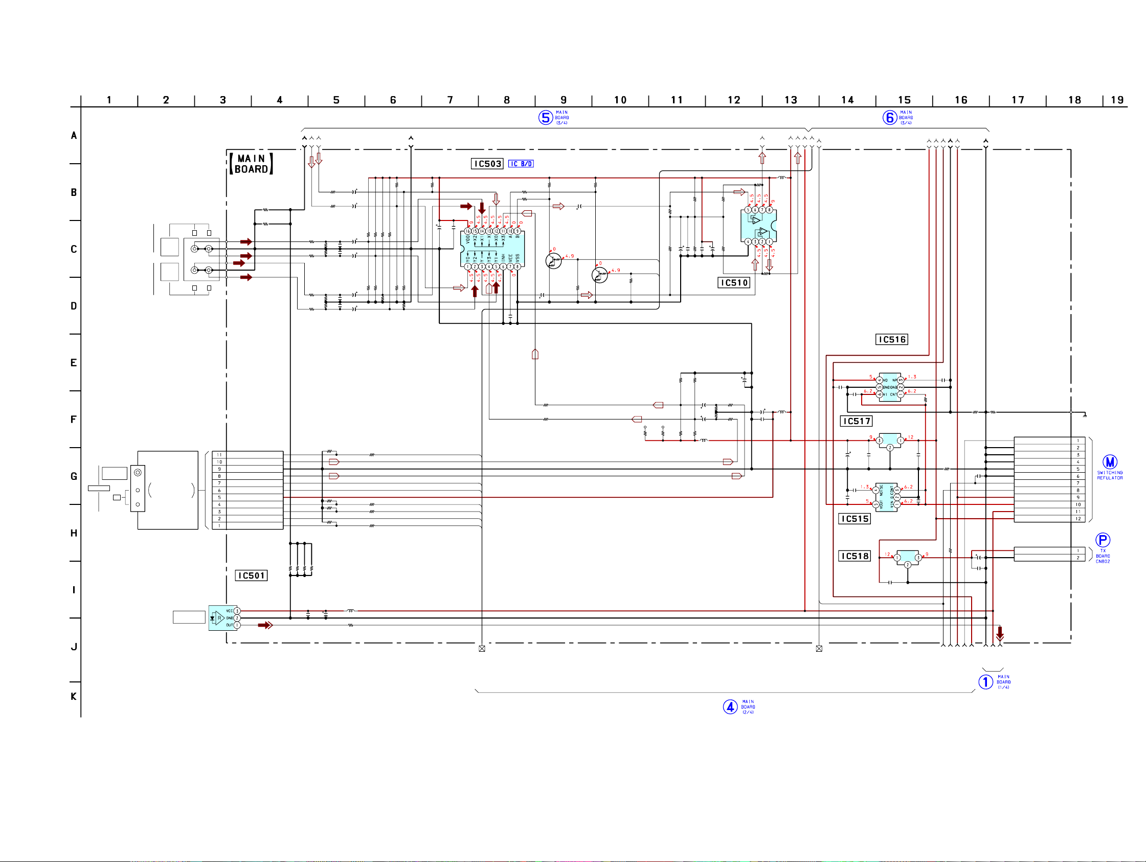
SA-WSLF10/SS-CTL10/TSL10/TSL11
5-9. SCHEMATIC DIAGRAM – MAIN Board (4/4) –
18
(4/4)
C614
0
C613
0
OPTICAL
DIGITAL IN
RL
RL
CN501
11P
MUTE
R-CH
A.GND
L-CH
STEREO
TUNED
CE
DI
DO
CK
0
0
0
C694
C693
C692
DIGITAL OPTICAL
RECEIVER
IC501
TORX141L
C501
0.1
ANTENNA
FM 75Ω
COAXIAL
VIDEO
AUDIO
IN
J501
4P
SAT
AUDIO
IN
TUNER UNIT
SUPPLIED WITH
THE ASSEMBLED
AM
BLOCK
• See page 34 for IC Block Diagrams.
17
16
R595
1k
C561
R594
100 10V
1k
C560
100
10k
10k
10V
527
525
C517
R
R
100
R514R510
C511
10V
47k6.8k
220p
C512R515R511
C518
220p47k6.8k
100
10V
10k
10k
528
C519
R526
R
100
C513
R516R512
10V
220p
47k6.8k
C520
C514R517R513
100
220p47k6.8k
10V
R505
R504
R503
R502
0
C691
C502
22
6.3V
L501
10µH
R501
R506
10k
10k
R508
10k
R509
R507
10k
100
15
R572R567
10k10k
10k
10k
R531
R535
10k
10k
10k
R568
R573
R532
R536
10k
4.7k
4.7k
4.7k
4.7k
C536
100
10V
MC14052
C537
IC503
BDR2
0.1
TU_MUTE
TU_STEREO3
TU_TUNED3
TU_DI3
TU_CLK
TU_DO
TU_CE
SELECTOR
(Page 18)
14
13
12
11
10
9
L508
470
R626R616
2.2k
C577
100
10V
1538 R534
100K 6.8k
NJM4565V
R628
2.2k
LINE AMP
R533R537
6.8k100k
R627
IC510
(TE2)
C616
10
16V
10µH
VCC
GND
R629
470
+5V REGULATOR
TK11250CMCL-G
C612
PCONT1
10
C611
+9V REGULATOR
C625
39
16V 0.1
C607
0.01
C608
10
+5V REGULATOR
IC515
MM1575ANLEG
+9V REGULATOR
1
BA09FP-E2
C624
C524
100
L502
10V
10µH
C521
0.001
Q503
DTC124EKA-
T146
R574
10k
R575R571
10k10k
4.7k
C563
100
10V
Q503,504
INVERTER
AVSEL1
AVSEL0
R578
10k
Q504
DTC124EKA-
T146
R565 R563 R561 R555
10k 10k 33k 33k
R596
47k
16V
0.1
10
4.7k
0.1
C567
C566
R617
47k
R593
R562
C576
R556
33k
33k
C531
22
16V
C530
22
16V
L504
10µH
R569
100
100
R570
C564
100
10V
C542
0.1
R552
0
R547
0
(Page 18)
6
5
4
3
IC516
IC517
IO
G
C623
IC518
BA09FP-E2
IO
G
C627
1
C626
0.1
R664
0
1
R647
0
C610
1
4.7k
R659
2
R641 C606
00
C675
0.1
C629
39
16V
C628
0.1
1
(CHASSIS)
CN506
12VREG-GND
12VREG-GND
VCC(9V)
P-GND
CN507
12P
(Page 33)
2P
AC-DET
A-GND
M-GND
M-GND
D-GND
D-GND
V-CONT
ON/OFF(STANDBY/POWER)
E5.6V9V
6.2V
3.3V
12V
(Page 27)
SA-WSLF10/SS-CTL10/TSL10/TSL11
ANALOG_CONT
D5V
PANEL_IF
PCONT1
V_CONT
E5.6V
AC_DET
D3.3V
DGND
OPT IN
(Page 16)
(Page 17)
1919
 Loading...