

Sony SRSDZ-10 Service manual
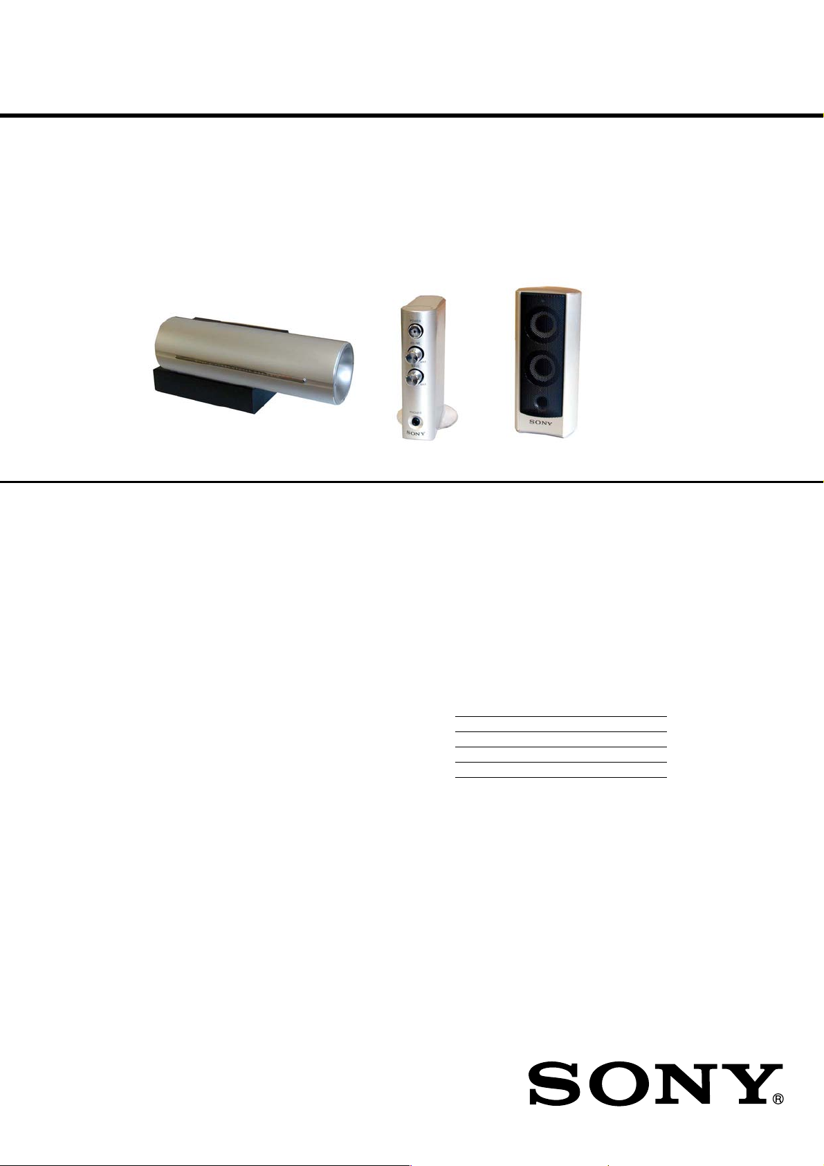
SRS-DZ10
SERVICE MANUAL
Ver. 1.1 2005.05
Subwoofer
Speaker section
Satellite speaker
Speaker system Magnetically shielded
Speaker units 3.9 cm, cone type (Sigma-type) × 2
Enclosure type Bass reflex
Impedance 8 Ω
Cord length 3 m
Subwoofer
Speaker system Active subwoofer, magnetically shielded
Speaker units 7.7 cm, cone type (Sigma-type)
Enclosure type Bass reflex
Impedance 8 Ω
Amplifier section
Rated output 6 W (10% T.H.D., 1 kHz, 8 Ω) (Satellite speaker)
25 W (10% T.H.D., 100 Hz, 8 Ω) (Subwoofer)
Input Stereo mini jack × 1 (INPUT 1)
Stereo mini jack × 1 (INPUT 2)
Input impedance 4.7 kΩ (at 1 kHz)
Output Stereo mini jack × 1 (PHONES)
Control Box
SPECIFICATIONS
US Model
Canadian Model
AEP Model
UK Model
Satellite
Speaker
General
Dimensions (w/h/d) Approx. 30 × 118.5 × 93.2 mm
(1 3/16 × 4 3/4 × 3 3/4 in.) (Control box)
Approx. ø62.8 × 142 mm
(2 1/2 × 5 in.) (Satellite speaker)
Approx. 375 × 151.5 × 183 mm
(14 7/8 × 6 × 7 1/4 in.) (Subwoofer)
Mass Approx. 146.5 g (6 oz.) (Control box)
Approx. 481 g (1 lb. 1 oz.) (Satellite speaker)
Approx. 4.1 kg (9 lb. 1 oz.) (Subwoofer)
Cord length 2 m (Control box to subwoofer)
2 m (Power cord)
Power requirements
Where purchased Operating voltage
U.S.A./Canada 120 V AC, 60 Hz
European countries 220 - 230 V AC, 50 Hz
Other countries 220 - 230 V AC, 50 Hz
Power consumptions 19 W (US, Canadian)
24 W (AEP, UK)
Supplied accessories
Connecting cord, rubber feet
9-879-587-02
2005E02-1
© 2005.05
Design and specifications are subject to change without notice.
ACTIVE SPEAKER SYSTEM
Sony Corporation
Personal Audio Group
Published by Sony Engineering Corporation
SRS-DZ10
SAFETY CHECK-OUT
After correcting the original service problem, perform the following
safety checks before releasing the set to the customer:
Check the antenna terminals, metal trim, “metallized” knobs, screws,
and all other exposed metal parts for AC leakage. Check leakage as
described below.
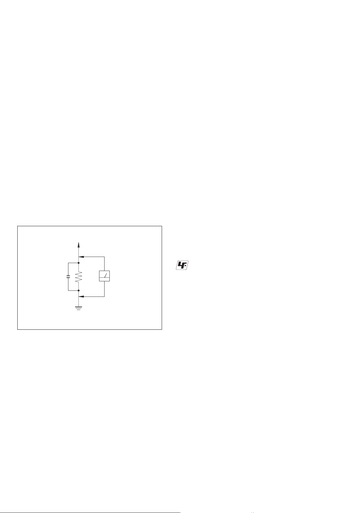
LEAKAGE
The AC leakage from any exposed metal part to earth Ground and
from all exposed metal parts to any exposed metal part having a
return to chassis, must not exceed 0.5 mA (500 microampers).
Leakage current can be measured by any one of three methods.
1. A commercial leakage tester, such as the Simpson 229 or RCA
WT-540A. Follow the manufacturers’ instructions to use these
instruments.
2. A battery-operated AC milliammeter. The Data Precision 245
digital multimeter is suitable for this job.
3. Measuring the voltage drop across a resistor by means of a
VOM or battery-operated AC voltmeter. The “limit” indication
is 0.75 V, so analog meters must have an accurate low-voltage
scale. The Simpson 250 and Sanwa SH-63Trd are examples
of a passive VOM that is suitable. Nearly all battery operated
digital multimeters that have a 2V AC range are suitable. (See
Fig. A)
To Exposed Metal
Par ts on Set
TABLE OF CONTENTS
Specifications ............................................................................ 1
1. GENERAL ................................................................... 3
2. DIAGRAMS
2-1. Printed Wiring Boards – Control Section–...................... 4
2-2. Schematic Diagram – Control Section– .......................... 5
2-3. Printed Wiring Boards– Amplifier Section (Side A) – .... 6
2-4. Printed Wiring Boards– Amplifier Section (Side B) – .... 7
2-5. Schematic Diagram – Amplifier Section– ....................... 8
2-6. Schematic Diagram – Satellite Section– ......................... 9
2-7. Printed Wiring Boards – Satellite Section– ..................... 10
3. EXPLODED VIEWS
3-1. Amplifier Section ............................................................ 10
3-2. Woofer Section ................................................................ 11
3-3. Control Box Section ........................................................ 12
3-4. Satellite Section ............................................................... 13
4. ELECTRICAL PARTS LIST .................................. 14
Unleaded solder
Boards requiring use of unleaded solder are printed with the lead
free mark (LF) indicating the solder contains no lead.
(Caution: Some printed circuit boards may not come printed with
the lead free mark due to their particular size.)
AC
0.15 µF
Fig. A. Using an AC voltmeter to check AC leakage.
1.5 kΩ
Earth Ground
Voltmeter
(0.75 V)
SAFETY-RELATED COMPONENT WARNING!!
COMPONENTS IDENTIFIED BY MARK 0 OR DOTTED LINE
WITH MARK 0 ON THE SCHEMATIC DIAGRAMS AND IN THE
PA RTS LIST ARE CRITICAL TO SAFE OPERATION. REPLACE
THESE COMPONENTS WITH SONY PARTS WHOSE PART
NUMBERS APPEAR AS SHOWN IN THIS MANUAL OR IN
SUPPLEMENTS PUBLISHED BY SONY.
: LEAD FREE MARK
Unleaded solder has the following characteristics.
• Unleaded solder melts at a temperature about 40°C higher than
ordinary solder.
Ordinary soldering irons can be used but the iron tip has to be
applied to the solder joint for a slightly longer time.
Soldering irons using a temperature regulator should be set to
about 350°C.
Caution: The printed pattern (copper foil) may peel away if
the heated tip is applied for too long, so be careful!
• Strong viscosity
Unleaded solder is more viscous (sticky, less prone to flow)
than ordinary solder so use caution not to let solder bridges
occur such as on IC pins, etc.
• Usable with ordinary solder
It is best to use only unleaded solder but unleaded solder may
also be added to ordinary solder.
ATTENTION AU COMPOSANT AYANT RAPPORT
À LA SÉCURITÉ!!
LES COMPOSANTS IDENTIFIÉS PAR UNE MARQUE 0 SUR LES
DIAGRAMMES SCHÉMATIQUES ET LA LISTE DES PIÈCES
SONT CRITIQUES POUR LA SÉCURITÉ DE FONCTIONNEMENT.
NE REMPLACER CES COMPOSANTS QUE PAR DES PIÈCES
SONY DONT LES NUMÉROS SONT DONNÉS DANS CE MANUEL
OU DANS LES SUPPLÉMENTS PUBLIÉS PAR SONY.
2
LOCATING THE CONTROLS
1
42 3
5
6
–
+
–
+
7 8 9
10 11
15
12 1413
–
+
–
+
OUT1+
OUT2+
OUT1-
OUT2-
VCC
VCC
IN1
IN2
OUTPUT 2
S-GND
PW-GND
ST-BY
MUTE
N.C.
N.C.
N.C.
Vref
1
42 3
5
6
–
+
–
+
7 8 9
10 11
15
12 1413
OUT
BOOTDIODE
BOOT
VREG
FEEDCAP
IN
-VCC SIGN
+VCC SIGN
+VCC POW
-VCC POW
-VCC POW
SGN-GND
ST-BY/MUTE
FREQ
N.C.
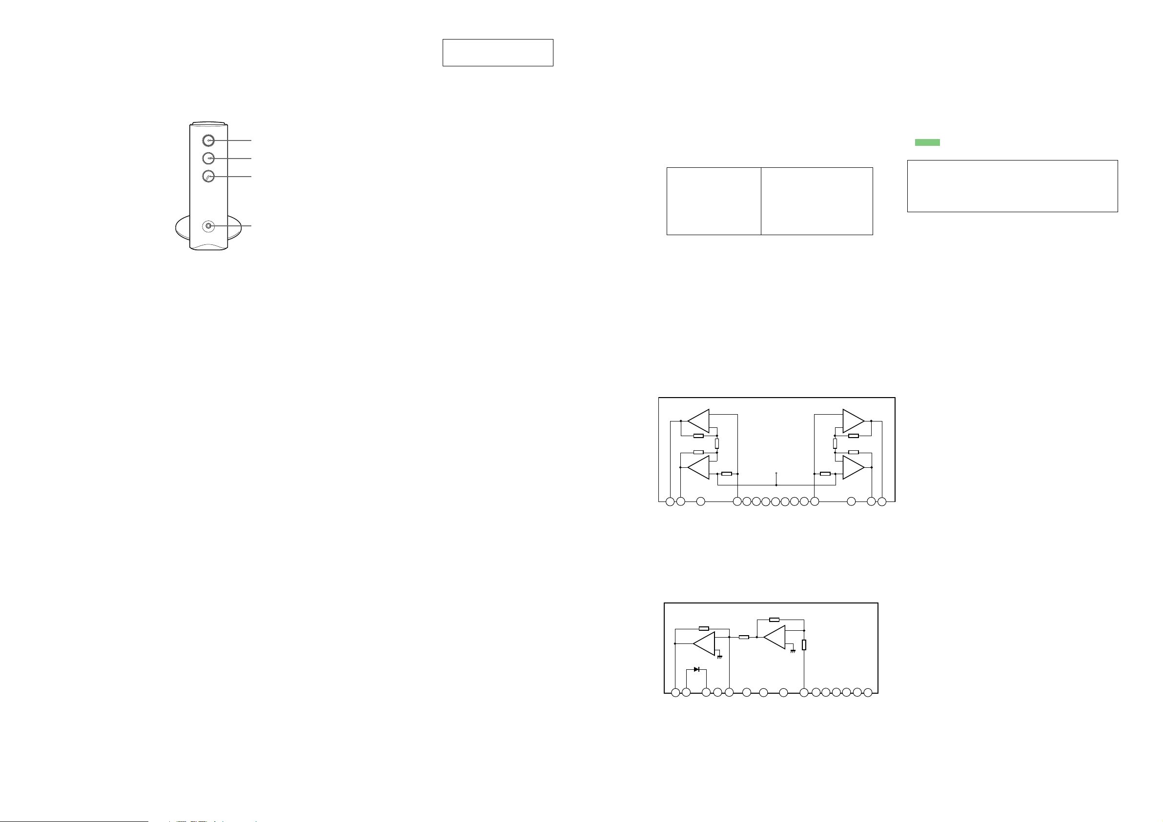
Control Box
POWER
VOLUME
BASS
PHONES
SRS-DZ10
SECTION 1
GENERAL
POWER
MAXMIN
MAXMIN
VOLUME
BASS
PHONES
VOLUME: Controls total volume level.
BASS: Adjusts bass level (Subwoofer).
PHONES: Connect to headphones for personal listening.
This section is extracted
from instruction manual.
THIS NOTE IS COMMON FOR PRINTED WIRING BOARDS AND SCHEMATIC DIAGRAMS.
(In addition to this necessary note is printed in each block.)
For schematic diagrams.
Note:
• All capacitors are in µF unless otherwise noted. (p: pF) 50 WV or
less are not indicated except for electrolytics and tantalums.
• All resistors are in Ω and 1/
• C : panel designation.
Note:
The components identified by mark 0 or dotted
line with mark 0 are criti-
cal for safety.
Replace only with part
number specified.
• A : B+ Line.
• B : B– Line.
•Voltages are dc with respect to ground under no-signal conditions.
• no mark : Power on
•Voltages are taken with a VOM (Input impedance 10 MΩ).
Voltage variations may be noted due to normal production tolerances.
• Signal path.
F : AUDIO
4
W or less unless otherwise specified.
Note:
Les composants identifiés par
une marque 0 sont critiques
pour la sécurité.
Ne les remplacer que par une
piéce portant le numéro
spécifié.
SECTION 2
DIAGRAMS
For printed wiring boards.
Note:
• X : parts extracted from the component side.
• : Pattern from the side which enables seeing.
(The other layers' patterns are not indicated.)
Caution:
Parts face side: Parts on the parts face side seen from
(Side A) the parts face are indicated.
Pattern face side: Parts on the pattern face side seen from
(Side B) the pattern face are indicated.
• IC Block Diagram
IC301 TDA7297
IC302 TDA7482
SRS-DZ10
33
SRS-DZ10
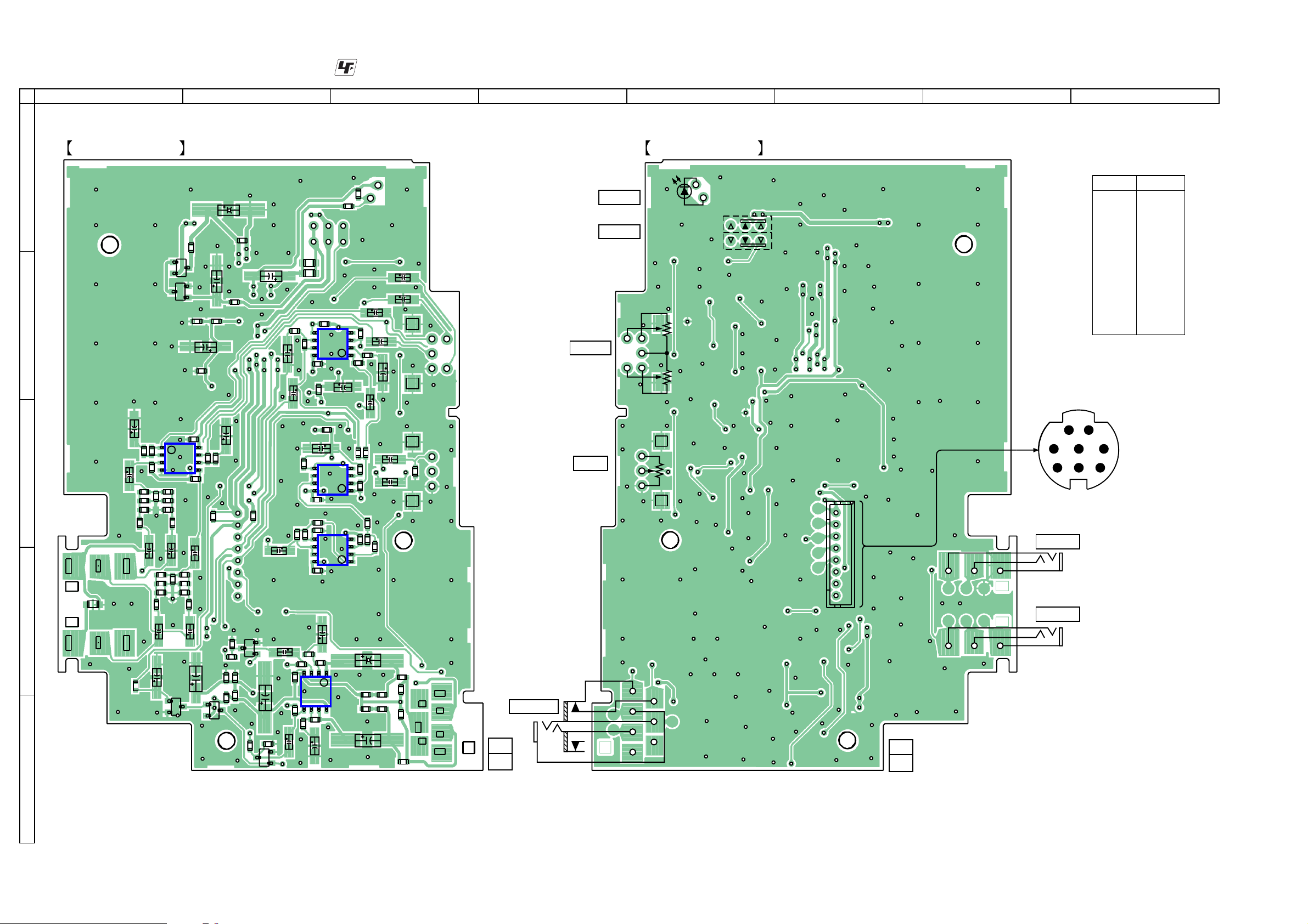
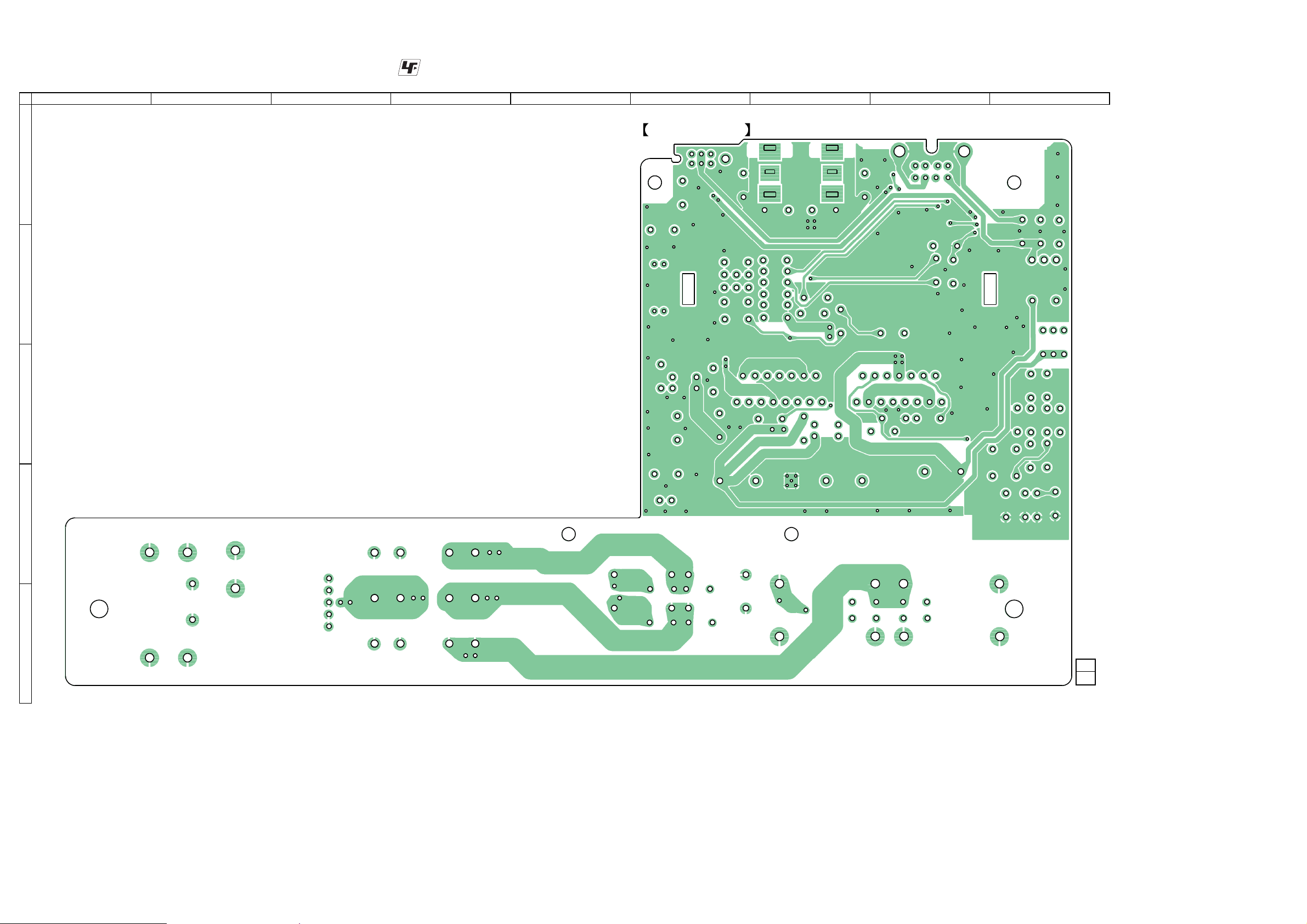
2-1. PRINTED WIRING BOARD – CONTROL SECTION –
1
2
CONTROL BOARD (SIDE A)
A
B
C
D
E
R302
Q103
E
Q104
R207
R132
R134
C151
C131
R203
R131
C322
Q102
IC101
1
R208
4
C201
R103
C316
E
C206
R204
C203
R232
R234
C251
R231
C231
C324
R322
R303
C331
R202
C250
R201
C101
E
C301
C302
8
R233
R102
R133
C150
R101
Q101
R301
5
R107
C323
C103
R211
R210
E
R108
C303
C321
C317
R321
C106
R104
Q205
R316
Q105
C304
C319
R318
R317
R110
C370
C116
C371
E
R212
R111
R118
R119
C111
R351
C368
R313
IC103
C325
C315
C212
C318
R112
R114
E
C112
R109
R325
C334
5
8
5
8
C333
R326
8
C213
R214
4
5
C330
R331
R353
R354
IC102
C332
C326
5
IC105
R213
1
8
R113
C113
: Uses unleaded solder.
3 4 5 6 7
C110
C210
C209
R209
C109
4
C369
R352
R115
1
R219
R307
R306
4
1
C312
4
R312
1
C214
IC104
C114
R218
C211
C336
R332
C310
R323
C313
R215
C215
C115
C216
R310
R216
R116
R217
R117
C309
1-867-133-
11
(11)
JK103
PHONES
RV102
VOLUME
RV103
BASS
D101
POWER
S101
POWER
CONTROL BOARD (SIDE B)
S101
t
OFF ON
–2
RV102
–1
RV103
1-867-133-
CN102
1
8
11
(11)
5
8
JK101
INPUT 1
JK102
INPUT 2
• Semiconductor
Location
Ref. No. Location
D101 A-5
IC101 C-1
IC102 B-3
IC103 C-2
IC104 D-2
IC105 D-3
Q101 E-2
Q102 E-1
Q103 B-1
Q104 B-1
Q105 E-2
Q205 D-2
2
1
4
3
7
6
8
SRS-DZ10
44
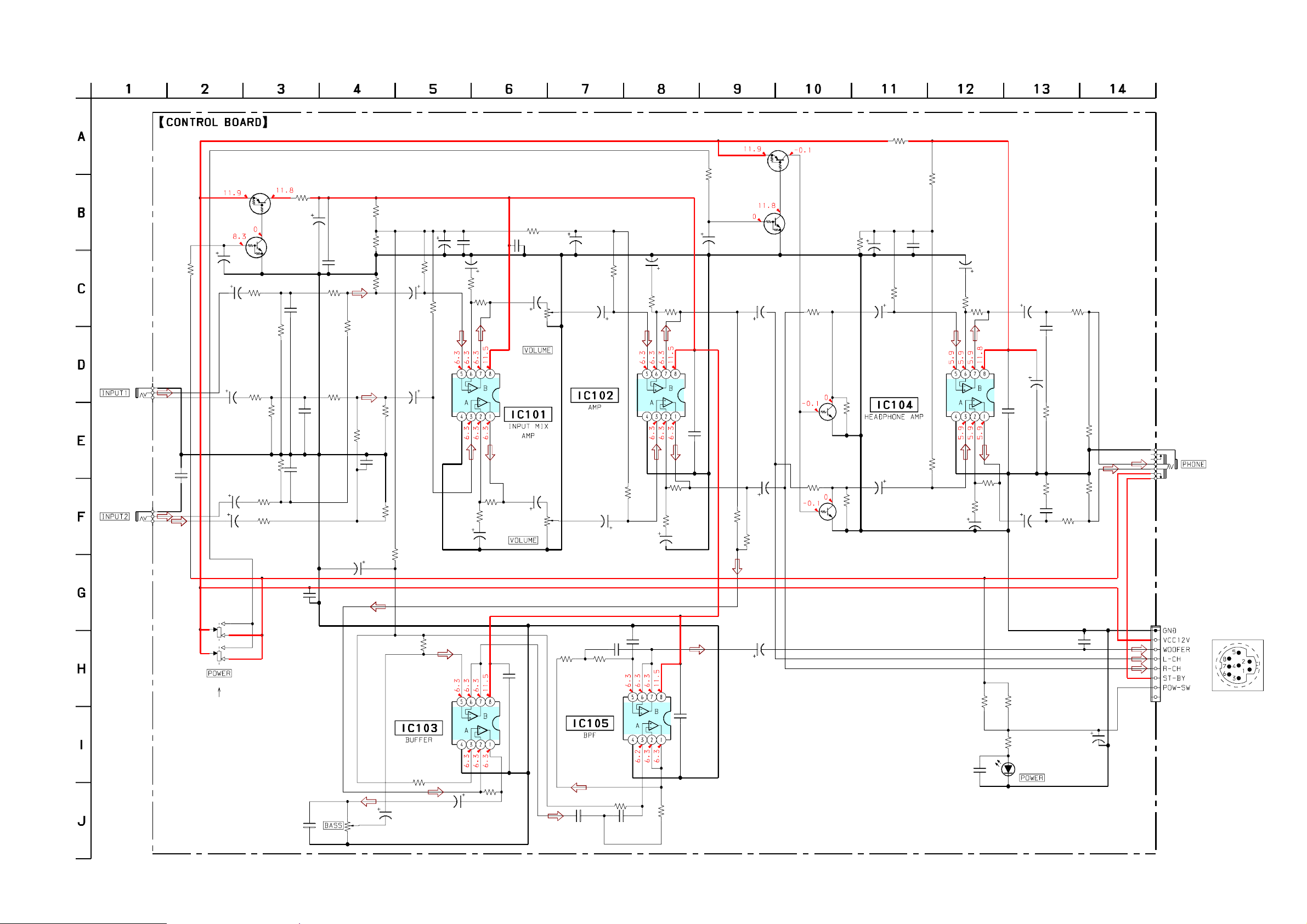
2-2. SCHEMATIC DIAGRAM – CONTROL SECTION –
SRS-DZ10
JK101
JK102
R321
4.7k
10
C324
C321
47
16V
C101
C201
4.7
25V
C131
4.7
25V
C231
4.7
25V
DTA114YKA
+B SWITCH
4.7
25V
Q103
R101
1k
R201
1k
R233
4.7k
R131
1k
R231
1k
R133
4.7k
R134
4.7k
Q104
DTC114YKA
+B SWITCH
R302
C303
220
16V
C150
1000p
C250
1000p
C151
1000p
Q101
DTA114YKA
R322
10k
Q102
0.1
C332
DTC114YKA
MUTE DRIVE
C322
22
16V
C111
4.7
25V
C211
4.7
25V
R306
10k
R307
10k
22
R102
6.8k
R132
6.8k
R202
6.8k
C304
0.1
R301
4.7k
R303
5.6k
C368
10
16V
R103
R232
6.8k
C251
1000p
R234
4.7k
1k
R203
R351
4.7k
R107
1k
22k
C103
C203
4.7
25V
4.7
25V
C301
100
6.3V
R207
22k
R104
1k
R204
C206
16V
10
C302
0.1
1k
C106
16V
R108
10k
10
C331
R208
10k
0.1
R352
4.7k
RV102(1/2)
10kA
IC101
µPC4558G2
RV102(2/2)
10kA
C109
4.7
25V
C209
4.7
25V
C369
10
16V
µPC4558G2
R109
22k
IC102
C110
4.7
25V
C210
4.7
25V
R118
6.8k
R209
22k
C116
C216
10
16V
16V
10
R119
22k
R219
22k
R218
6.8k
MUTE DRIVE
R110
10k
Q105
DTC343TK
MUTE
R210
10k
Q205
DTC343TK
MUTE
R318
4.7k
R111
1.5k
R211
1.5k
R316
22
C316
100
6.3V
R112
22k
C112
4.7
25V
IC104
NJM4580M-(TE2)
C212
4.7
25V
C317
0.1
R212
R317
4.7k
22k
R114
1k
C113
R214
1k
16V
10
C114
R113
C213
10
16V
10k
R213
10k
C319
220
16V
220
6.3V
C318
0.1
R215
C214
220
6.3V
4.7
C115
0.22
R115
4.7
C215
0.22
R117
R216
4.7
220
R116
4.7
R217
220
JK103
SRS-DZ10
S101(1/2)
PUSH-SW
3-2
OFF
ON
C323
100p
S101(2/2)
PUSH-SW
3-2
C309
0.1
RV103
10k
µPC4558G2
C310
4.7
25V
R313
IC103
R332
22k
22k
C336
4.7
25V
C333
0.1
R323
22k
R325
15k
NJM4558M
C312
0.068
IC105
R326
12k
C325
0.22
R312
100k
C313
0.068
C326
0.068
CN102
8P
1
8
R310
15k
C334
0.1
C315
4.7
25V
C330
0.1
R353
4.7
R354
4.7
R331
470
D101
TLG124A
C371
1000p
C370
16V
47
55
SRS-DZ10
2-3. PRINTED WIRING BOARD – AMPLIFIER SECTION (SIDE A) –
1
A
B
2
3 4 5 6 7
: Uses unleaded solder.
8
BOARDAMPLIFIER
(SIDE A)
9
C
D
E
21
1-867-135-
(21)
SRS-DZ10
66
 Loading...