

Sony SPP-Z750PC Service Manual
SRS-Z750/Z750PC
SERVICE MANUAL
Ver 1.0 1998. 07
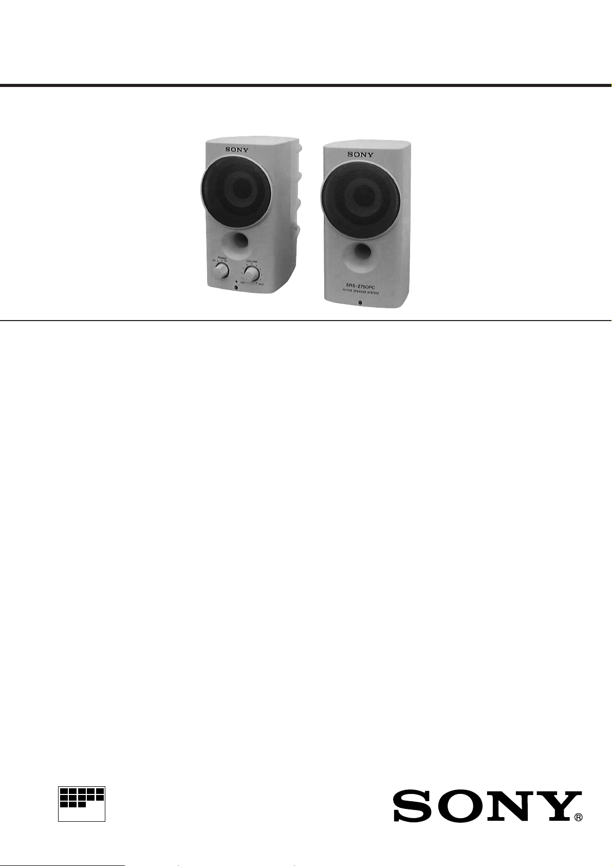
Left
speaker
Photo: SRS-Z750PC
SPECIFICATIONS
Amplifier section
Power output 7.5 W + 7.5 W
Input impedance 4.7 Kilohms (at 1 kHz)
Input Stereo mini jack (INPUT)
(SRS-Z750)
Stereo mini jack × 2 (INPUT 1, 2)
(SRS-Z750PC)
US Model
Canadian Model
AEP Model
UK Model
E Model
Austr alian Model
Right
speaker
Speaker section
System Full-range, bass reflex type
Speaker unit Magnetically shielded ø65 mm
Nominal Impedance 8 ohms
Rated input power 7.5 W
General
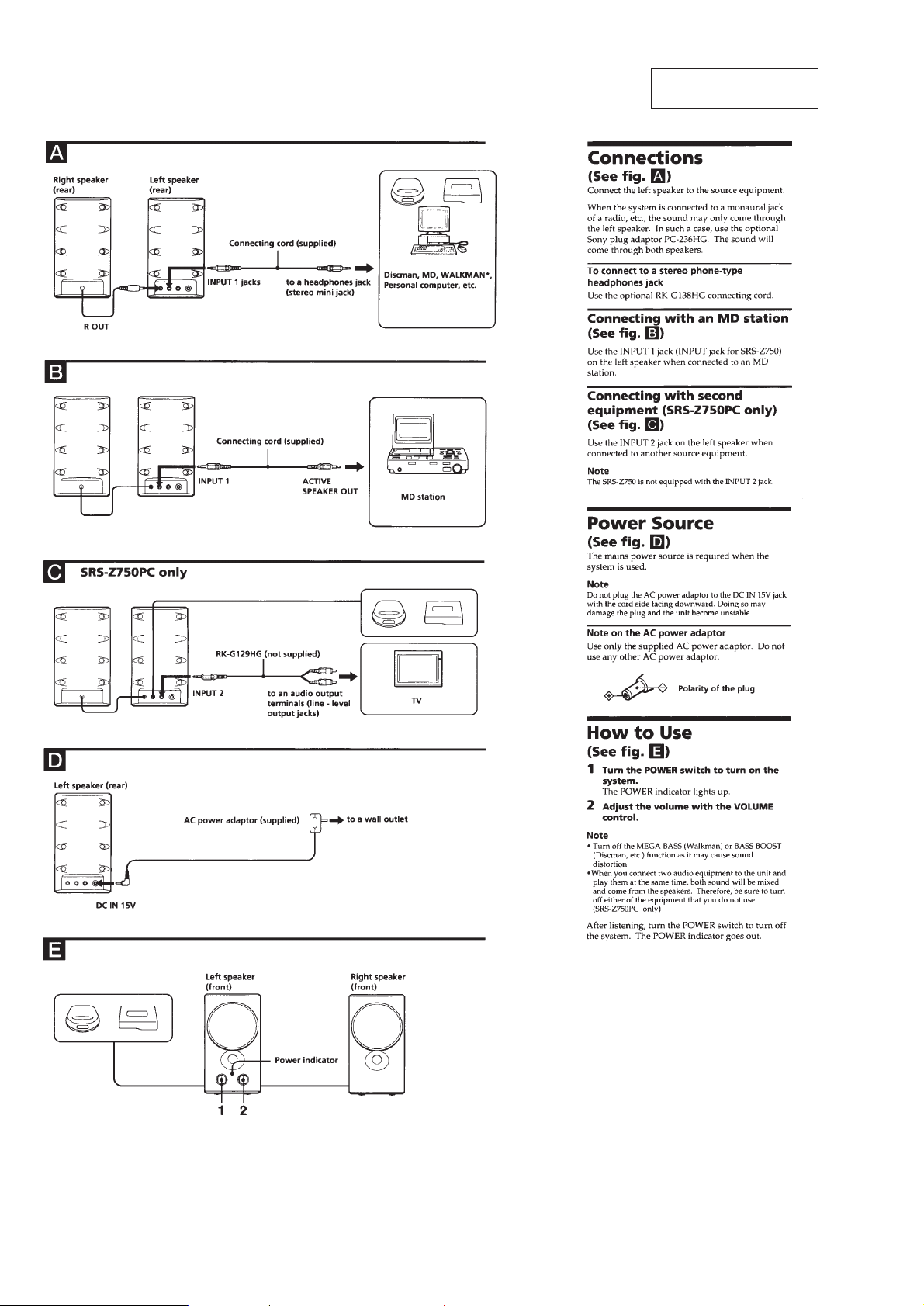
Power requirement DC IN 15 V jack accepts the
Dimensions Approx. 90 × 165 × 155 mm (3 5/8 ×
Mass Left speaker: Approx. 850 g (1 lb. 14 oz.)
Supplied accessories AC power adaptor AC-S1510 (1)
Design and specifications are subject to change without
notice.
The CE mark on the unit is valid only for products
marketed in the European Union.
(2 5/8 inch)
supplied Sony AC power adaptor
(left speaker only)
6 1/2 × 6 1/8 in.) (w/h/d) incl.
projecting parts and controls
Right speaker: Approx. 750 g (1 lb. 10 oz.)
Connecting cord (stereo miniplug
˜ stereo miniplug) (1)
MICROFILM
STEREO ACTIVE SPEAKER SYSTEM
– 1 –
SECTION 1
GENERAL
This section is extracted
from instruction manual.
– 2 –
SECTION 2
DIAGRAMS
SRS-Z750/Z750PC
2-1. PRINTED WIRING BOARD (SRS-Z750)
2-2. SCHEMATIC DIAGRAM (SRS-Z750)
• Semiconductor
Location
Ref. No. Location
D1 D-2
D2 D-3
D3 F-2
D4 F-2
IC1 D-2
Q1 E-3
Q2 E-3
Note:
• X : parts extracted from the component side.
• Y : parts extracted from the conductor side.
• b : Pattern from the side which enables seeing.
Note:
• All capacitors are in µF unless otherwise noted. pF: µµF
50 WV or less are not indicated except for electrolytics
and tantalums.
• All resistors are in Ω and 1/
specified.
4
W or less unless otherwise
• C : panel designation.
• U : B+ Line.
• Power voltage is dc 15 V and fed with regulated dc power
supply from external power voltage jack.
• Voltage is dc with respect to ground under no-signal
condition.
• V oltages are taken with a VOM (Input impedance 10 MΩ).
Voltage variations may be noted due to normal production tolerances.
• Signal path.
F : AUDIO
• IC Block Diagram
IC1 LA4663
RIPPLE FILTER/
STARTING TIME
IN1
PRE GND
IN2
STANDBY
SIGNAL MUTE
VCC1
VCC2
+OUT2
POWER GND2
–OUT2
–OUT1
POWER GND1
+OUT1
INPUT
AMP
1
2
3
4
5
6
INPUT
7
AMP
8
9
10
11
12
13
14
+
OUTPUT
–
AMP
+
OUTPUT
–
AMP
– 3 – – 4 –
 Loading...