

Page 1
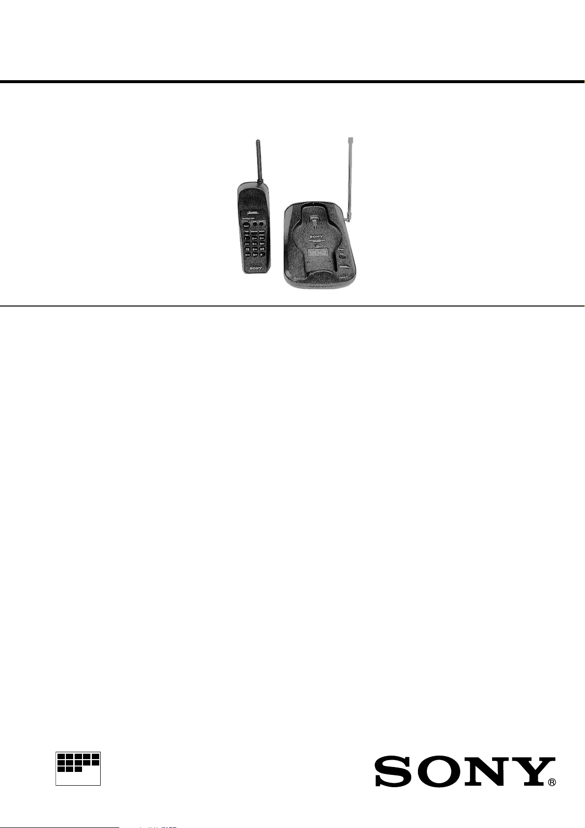
SPP-SS950
SERVICE MANUAL
Ver 1.2 2000. 06
With SUPPLEMENT-1
(9-925-727-81)
SPECIFICATIONS
General
Spread method Direct-Sequence Spread-Spectrum
Access method FDMA-TDD
Frequency band 902 – 928 MHz
Operation channel 20 channels
Supplied Accessories AC power adaptor AC-T37 (1) (US model)
AC power adaptor AC-T47 (1) (E model)
Telephone line cords (2) (US model)
Telephone line cord (1) (E model)
Rechargeable battery pack BP-T18 (1)
Directories (2 sheets)
Wall bracket/stand (1)
Screws (2) (E model)
US Model
E Model
Base unit
Power source DC 9V from AC power adaptor
Battery charging time Approx. 12 hours
Dimensions Approx. 128 × 58 × 208 mm (w/h/d), antenna
excluded
Antenna: 165 mm
Mass Approx. 320 g, wall bracket excluded
Design and specifications are subject to change without notice.
Handset
Power source Rechargeable battery pakc BP-T18
Battery life Standby: Approx. 7 days (RING ON mode)
Approx. 3 weeks (BATT SAVE mode)
Talk: Approx. 4 hours
Dimensions Approx. 58 × 177 × 46 mm (w/h/d), antenna
excluded
Antenna: 72 mm
Mass Approx. 250 g, battery included
CORDLESS TELEPHONE
MICROFILM
Page 2

TABLE OF CONTENTS
SERVICING NOTES
1. GENERAL
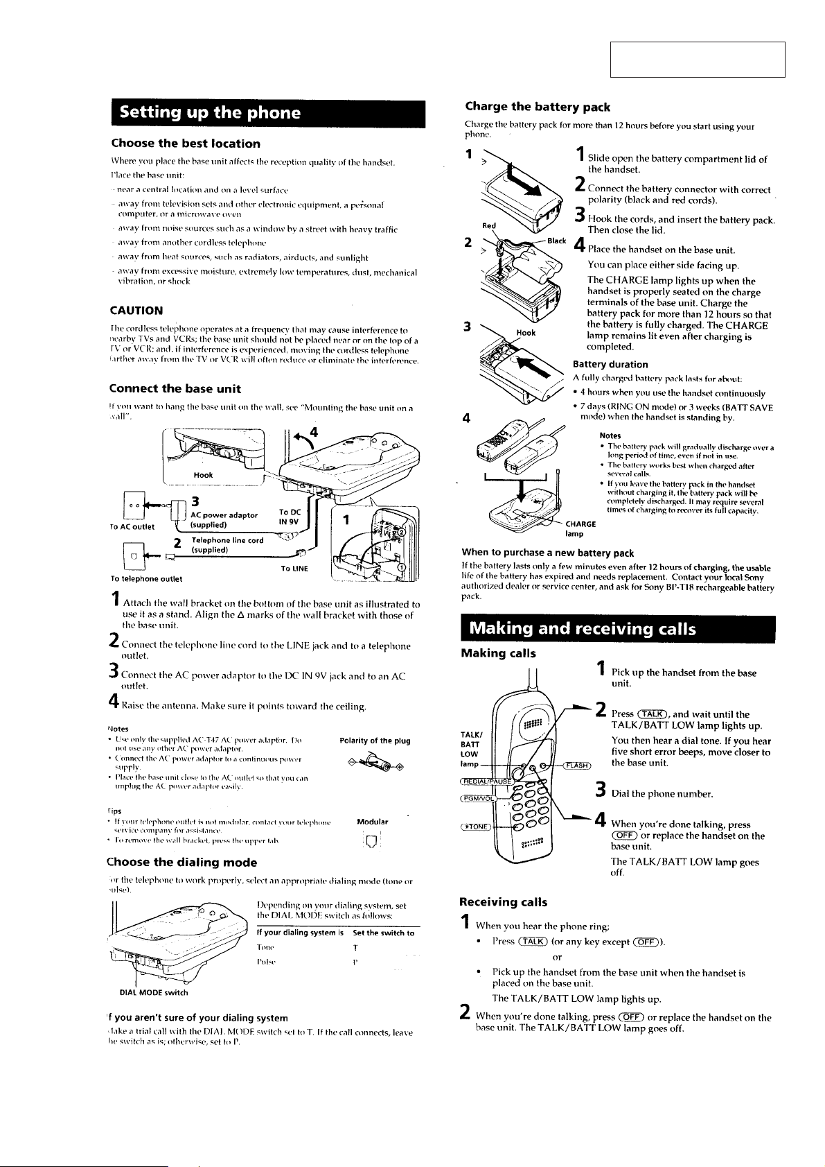
Setting up the phone ........................................................3
Making and receiving calls.............................................. 3
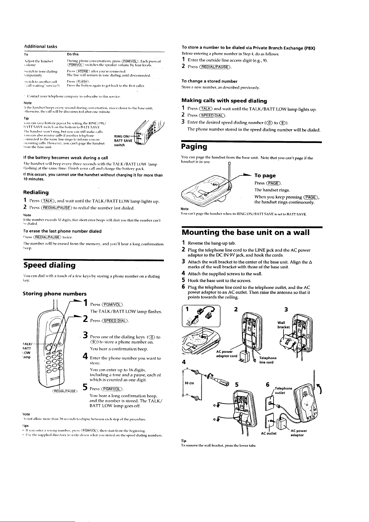
Speed dialing ................................................................... 4
Paging .............................................................................. 4
Mounting the base unit on a wall .................................... 4
2. DISASSEMBLY..........................................................5
3. 900MHz SYSTEM OPERATION
3-1. Access method ................................................................. 7
3-2. Protocol............................................................................7
4. TEST MODE
4-1. Base Unit Test Mode A.................................................... 10
4-2. Base Unit Test Mode B....................................................10
4-3. Handset Test Mode .......................................................... 1 1
5. ELECTRICAL ADJUSTMENTS
5-1. Base Unit Section ............................................................ 12
5-2. Handset Section ...............................................................13
6. DIAGRAMS
6-1. Schematic Diagram – Base Unit Section –...................... 16
6-2. Printed Wiring board – Base Unit Section – ................... 19
6-3. Printed Wiring Board – Handset Section –...................... 21
6-4. Schematic Diagram – Handset Section – ........................ 23
6-5. IC Pin Function Description ............................................26
Flexible Circuit Board Repairing
• Keep the temperature of the soldering iron around 270 ˚C during
repairing.
• Do not touch the soldering iron on the same conductor of the
circuit board (within 3 times).
• Be careful not to apply force on the conductor when soldering or
unsoldering
Notes on chip component replacement
• Never reuse a disconnected chip component.
• Notice that the minus side of a tantalum capacitor may be dam-
aged by heat.
SAFETY-RELATED COMPONENT WARNING!!
COMPONENTS IDENTIFIED BY MARK ! OR DOTTED LINE
WITH MARK ! ON THE SCHEMATIC DIAGRAMS AND IN
THE PARTS LIST ARE CRITICAL TO SAFE OPERATION.
REPLACE THESE COMPONENTS WITH SONY P ARTS WHOSE
PART NUMBERS APPEAR AS SHOWN IN THIS MANUAL
OR IN SUPPLEMENTS PUBLISHED BY SONY.
7. EXPLODED VIEWS ................................................ 30
8. ELECTRICAL PARTS LIST................................ 32
– 2 –
Page 3
SECTION 1
GENERAL
This section is extracted from
instruction manual.
– 3 –
Page 4
– 4 –
Page 5
SECTION 2
DISASSEMBLY
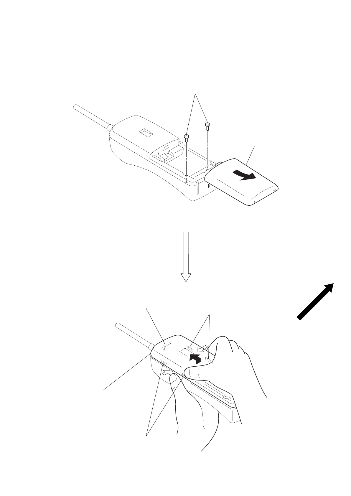
Note: Follow the disassembly procedure in the numerical order given.
REAR CABINET
2
two screws
(BTP 2.6 × 10)
1
Remove the battery case lid
to direction of the arrow A.
A
5
Remove the rear cabinet to
direction of the arrow B.
3
4
claw
two claws
B
3
two claws
– 5 –
Page 6
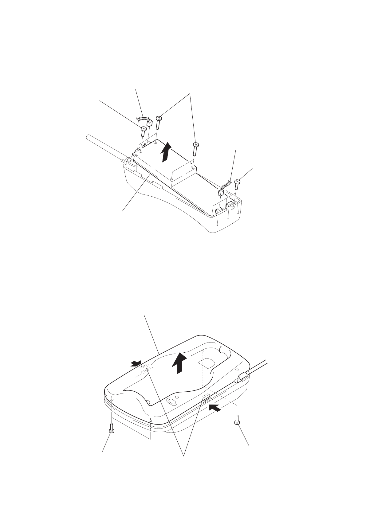
HAND MAIN BOARD
3
screw
(BTP 2.6 × 8)
1
connector
4
HAND MAIN board
2
four screws
(P 3 × 16)
1
connector
3
three screws
(BTP 2.6 × 8)
LOWER CABINET
1
two screws
(BTP 2.6 × 8)
3
lower cabinet
2
two claws
1
two screws
(BTP 2.6 × 8)
– 6 –
Page 7
SECTION 3
900MHz SYSTEM OPERATION
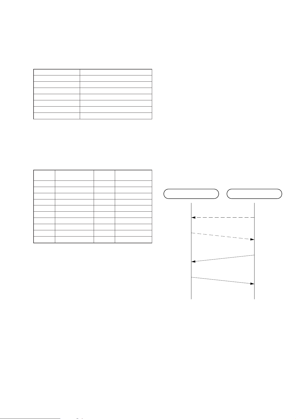
3-1. ACCESS METHOD
1. Transfer format & rate
The transfer format & rate of our system is as follows;
Table 3-1. Transfer method
Access method FDMA-TDD
Channel number 20 channel
Channel spacing 1.2MHz
Modulation method DBPSK
Baseband transfer rate 960Kbps
Spread method Direct Sequence Spread Spectrum
Chip rate 12 chips/bit
Data transfer rate 80 Kbps
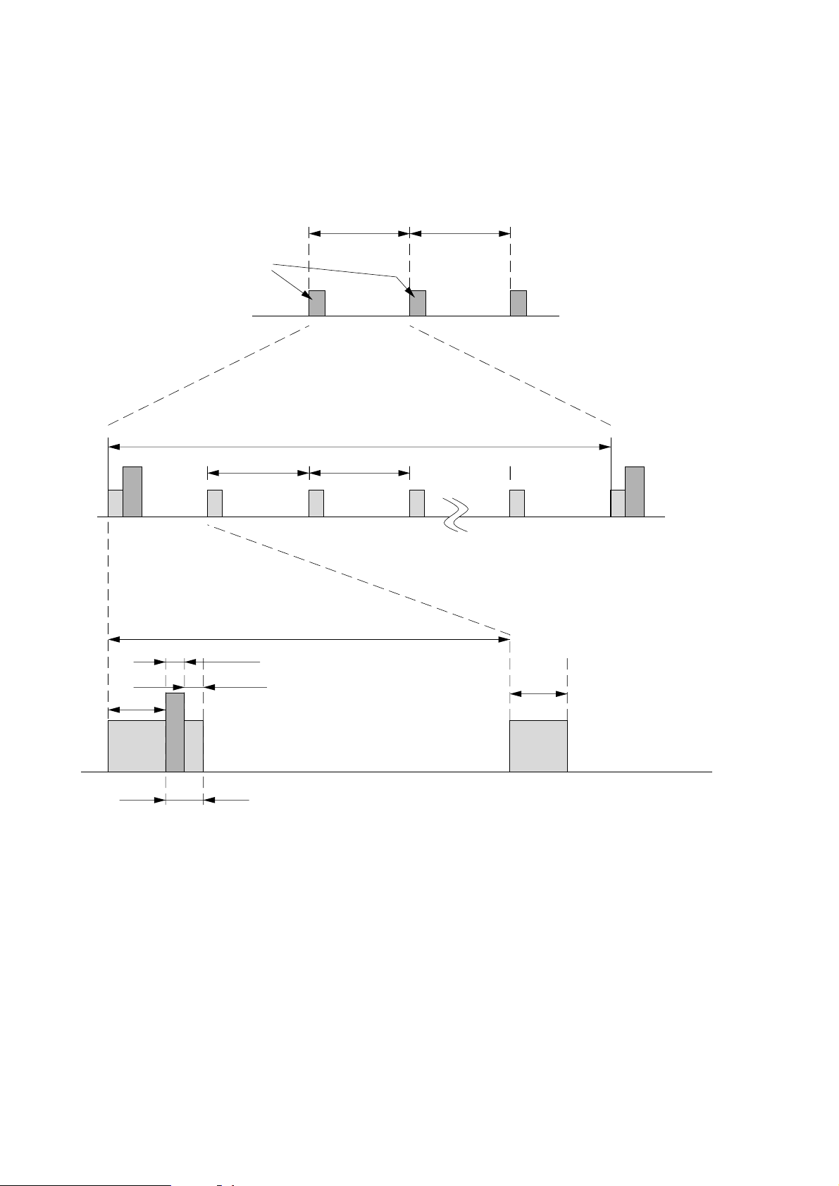
2. Channel Number & Frequencies
RF channels occupy the frequency band 902 – 928 MHz are numbered 1 to 20.
RF channel numbers & center frequencies are specified as follows.
Table 3-2. Channel number & Channel frequency
Channle Channel Center Channel Channel Center
Number Frequency (MHz) Number Frequency (MHz)
1 903.6 11 915.6
2 904.8 12 916.8
3 906.0 13 918.0
4 907.2 14 919.2
5 908.4 15 920.4
6 909.6 16 921.6
7 910.8 17 922.8
8 912.0 18 824.0
9 913.2 19 925.2
10 914.4 20 926.4
3-2. PROTOCAL
1. General
This system realizes the TX/RX superframe by TDD system. The
relation of master/slave dose not decide identification regarding
the protocol between BS and HS, but the initiated side is the master and the requested side is the slave when the RF link has been
established.
2. Initial acquistition
In order to establish the RF link between BS and HS, both of BS
and HS need to have the same system ID. When “power” is applied to this system, the system have to do Initial Acquisition in
order to have the same system ID. It si to exchange a parameter
when the HS is parked on the BS, as soon as the system do System
Parameters Re-initilization.
3. System parameter re-initilization
This System Parameters Re-initilization can realize that the HS is
parked on the BS. So after the BS recoginized to be parked the
HS, the BS calculates a system parameter, and then it outputs this
data from the ARTO port, and then the system establishs the RF
link. In order to establish this link, the HS send the A-Frame to the
BS after the HS received the system parameter, and then the BS
send the A-Frame to the HS. The process of System Parameters
Re-initilization is as follows.
Base Station Handset
(PARK)
(Park Detect)(Park Detect)
System Parameters
A-Frame
System ID
confirmed
A-Frame
Fig. 3-1. System Parameters Re-initialization
System ID
confirmed
– 7 –
Page 8
4. Stand-by Mode Operation
(1) HS
When the HS is the stand-by mode (sleep mode), the HS do the
intermittent operation for power save, because the HS is the battery operation.
This process of stand-by mode operation is as follows.
10 sec
Heart-Beat
10 sec
Heart-Beat Heart-Beat
RX RX RX RX RX
1 sec 1 sec
RX
10 sec
1 sec
2 msec
2 msec 10 msec
10 msec
RXTXRX
Heart Beat
(Exchange A-Frame for Link confirmation purpose)
Fig. 3-2. Stand-by mode operation (HS)
(2) BS
The BS is supplied the power by AC line. While the BS is the
stand-by, the BS is always a wake state. While the BS monitors
the current channel, the BS monitors also the other channel at the
same time
Because if the current channel can not use by some interference,
the system needs the clear channel information as a part of system
parameter for a channel hop.
If the BS can not receive the A-Frame of Heart-beat from the HS,
it become “link error”, and the system become error recovery mode.
RX
– 8 –
Page 9
5. Link Establishment
Accoding to the following Fig. 3-1, the requested side for link
establishment is the master.
The system have to exchange the A-Frame for link establishment,
and each system ID should be the same ID, and then the system
link is established.
The protocol and timing chart of link establishment are as follows.
Master Slave
A-Frame
System ID
confirmed
Fig. 3-3. Link Establishment protocol
A-Frame
V-Frame
V-Frame
V-Frame
V-Frame
System ID
confirmed
Master
Time Slot
Master TX
Master RX
Slave RX
Slave TX
Trip Delay
TX RX TX RX TX
AV
A' V
Fig. 3-4. Link Establishment Timing Chart
6. State Change/Tarmination
After the RF link between HS and BS was established, a movement of each state (State: ON-Hook, OFF-Hook, P A GE, InterCom,
etc) is sent through supervisory bits.
V
VA
VA'
V
V
7. Error Recovery
In case of the following situation, The system becomes “Error
Recovery Mode”.
(1) The system failed to move to “Heart-Beat” during “Stand-by
mode, or failed “link establishment”.
(2) The system failed to keep the link.
– 9 –
Page 10
SECTION 4
TEST MODE
4-1. BASE UNIT TEST MODE A
[Start-up]
1. Set [DIALMODE] switch to the P (PULSE) side.
2. With [PAGE] button kept pressed, reset the POWER ON (connect the A C adapter plug) and return [DIALMODE] switch from
P (PULSE) side to T (TONE) side, then again to the P (PULSE)
side.
3. Release the [PAGE] button, and the Test Mode A will start.
4. When the Test Mode A started, the Dial Test is carried out.
5. If [DIALMODE] switch is changed over from P (PULSE) to T
(TONE) side, the base set goes in Test Mode Idle A status.
[Dial Test]
1. When the Test Mode started, a line is connected.
2. “0” is output with 10pps (PLUSE) signal.
3. After 2 seconds, “1” “4” “8” “#” are output with DTMF
(TONE) signals.
4. Then, the line is placed in the busy status.
[TDD Test Mode on Each Channel]
1. In the Test Mode Idle A status, the statused of respectiv e blocks
are as follows:
Radio block – TDD mode (Master timing, 1CH)
Audio block – Line busy status
2. Each time [PAGE] button is pressed, channels are changed ov er
as follows:
4-2. BASE UNIT TEST MODE B
[Start-up]
1. Set [DIALMODE] switch to the T (TONE) side.
2. With [PAGE] button kept pressed, reset the POWER ON (connect the A C adapter plug) and return [DIALMODE] switc h from
T (TONE) side to P (PULSE) side, then again to the T (TONE)
side.
3. Release the [PAGE] button, and the Test Mode B will start.
4. In the Test Mode B, two kinds of idle statuses can be selected
depending on the[DIALMODE] switch setting.
DIAL MODE switch Idle statuses
T (TONE) side Test Mode Idle B-1 *1
P (PULSE) ise Test Mode Idle B-2 *2
*1: Radio block – TDD mode (Master timing)
Audio block – Line busy status
*2: Radio block – Standby status
Audio block – Line open
[Charging Detection Test, ARTO Pin Output Test, and
EEPROM Clear]
1. In the Test Mode Idle B-1 status, if charging is detected, a rectangular wave of 2.4 kHz is output from the IC751 Pin #¢
(ART0 pin).
2. At this time, the contents of the EEPROM memory are all
clearered.
Test Mode
Idle A → 2CH → 3CH → 4CH → . . . → 20CH
(1CH)
↑
3. On the channels 2 to 20, the statuses of respective blocks are as
follows:
Radio block – TDD mode (Slave timing)
Audio block – Line busy status
[Charging Detection Test, ARTO Pin Output Test, and
EEPROM Clear]
1. In the Test Mode Idle A status, if charging is detected, a rectangular wave of 2.4 kHz is output from the IC751 Pin #¢ (ARTO
pin).
2. At this time, the contents of the EEPROM memory are all
cleared.
[Terminating Signal Detection Test]
1. In the Test Mode Idle B-2 status, if a terminating signal is
detected, H → L → . . . are output from the IC751 Pin *ª in
synchronization with H → L → . . . of terminating signal detected.
[Continuous Receive Mode, Continuous Transmit Mode
and TDD Test Mode with High, Mid, and Low Power]
In the T est Mode Idle B-2 status, each time [PAGE] button is pressed,
the mode changes as follows:
[PAGE] button
pressing times
1 CONT. RECEIVE (1CH, LNA ON, AGC ON)
2 CONT. RECEIVE (10CH, LNA ON, AGC ON)
3 CONT. RECEIVE (20CH, LNA ON, AGC ON)
4 CONT. TRANSMIT (1CH, High power)
5 CONT. TRANSMIT (1CH, Mid power)
6 CONT. TRANSMIT (1CH, Low pwer)
7 CONT. TRANSMIT (10CH, High pwer)
8 CONT. TRANSMIT (10CH, Mid pwer)
9 CONT. TRANSMIT (10CH, Low pwer)
10 CONT. TRANSMIT (20CH, High pwer)
11 CONT. TRANSMIT (20CH, Mid pwer)
12 CONT. TRANSMIT (20CH, Low pwer)
13 TDD Mode (Master timing, 1CH, High power)
14 TDD Mode (Master timing, 1CH, Mid power)
15 TDD Mode (Master timing, 1CH, Low power)
16 Return to Test Mode Idle B-2
* In the statuses of 1 – 15, the audio block is placed in the line busy status.
Radio Block
– 10 –
Page 11

4-3. HAND SET
[Key Matrix Test Mode and LED Test Mode]
[Start-up]
1. With the po wer supplied, press [TALK] [0] [1] keys simultaneously ,
and the Test Mode will start.
2. Immediately after the Test Mode started, the ringer sounds for
500 msec, and the handset goes in Test Mode Idle status.
3. In the Test Mode Idle status, the statuses of respective blocks
are as follows:
Radio block – TDD Mode (Master timing, 1CH)
Audio block – Line busy status
4. In the Test Mode Idle status, respective test modes can be executed by key input properly.
5. In respective test modes, the Test Mode Idle status is resumed
by entering “0 1 #” keys.
6. In any mode, if “0 0 #” keys are entered, the Test Mode is cancelled and normal operating condition is resumed.
[Continuous Receive Mode]
1. Enter “1 1 #” keys, and the Continuous Receive (1CH, LHA
ON, AGC ON) mode is activated.
2. Each time [*] key is pressed, channels are changed over as follows:
1CH → 2CH → 3CH → 4CH → . . . → 20CH
↑
[Continuous T ransmit mode]
1. Enter “2 1 #” keys, and the Continuous Transmit (1CH, High
power) mode is activated.
2. Enter “2 2 #” key to activate Continuous Transmit (1CH, Mid
power) mode.
3. Enter “2 3 #” key to activate Continuous Transmit (1CH, Low
power) mode.
4. In respective modes, each time [*] key is pressed, channels are
changed over as follows:
1CH → 2CH → 3CH → 4CH → . . . → 20CH
↑
• Key Matrix Test mode
1. Enter “5 1 #” keys, and the Key Matrix Test mode is activated.
2. If pressing the keys in the order shown below, an acknowledge
tone is output. Or, if pressing other keys, and error tone will be
output.
[TALK] → [OFF] → [FLASH] → [PGM/VOL] → [SPEEDDIAL] →
[REDIAL/PAUSE] → [1] → [2] → [3] → [4] → [5] → [6] → [7] →
[8] → [9] → [*] → [0] → [#]
3. When an acknowledge tone or error tone is output, the initial
status of key matrix test and LED test mode is activated. From
this status, the key matrix test and LED test can be executed
with the key input.
• LED Test mode
1. Enter “5 4 #” keys, and the LED Test mode is activated.
2. When LED Test mode started, all LEDs turn on immediately.
[TDD Test Mode on Each Channel]
1. Enter “6 1 #” keys, and the TDD mode (Master timing, 1CH,
Line busy status) is activated.
2. Each time [*] key is pressed, channels are changed over as follows:
1CH → 2CH → 3CH → 4 CH → . . . → 20CH
↑
[EEPROM Clear]
Enter “7 1 #” keys, and the contents of EEPROM memory are all
cleared.
[Loopback T est Mode]
Key input Test mode
31# Code Forward Loopback (L1)
32# ADPCM Forward Loopback (L2)
33# ADPCM → RADIO Loopback
34# ADPCM Reverse Loopback
[TDD Test Mode with High, Mid, and Low Power]
Key input
41#
42#
43#
44#
Radio block
TDD mode (Master timing,
1CH, High power)
TDD mode (Master timing,
1CH, Mid power)
TDD mode (Master timing,
1CH, Low power)
TDD mode (Slave timing)
Audio block
Line busy status
Line busy status
Line busy status
Standby status
– 11 –
Page 12

SECTION 5
L
L
L
ELECTRICAL ADJUSTMENTS
5-1. BASE UNIT SECTION
• Make the set in Test mode (see page 10)
1. Checking RX I&Q Output Level
Setting:
oscilloscope
+
–
SG
Procedure:
1. Place the base unit in the Continous Receive mode (1CH, LNA
ON, AGC ON).
2. Set the SSG frequency to the frequency on 1CH + 300 kHz,
and the RF output level to –95 dBm.
3. Measure the output level of RXIN, RXIP, RXQN and RXQP
with a level meter. At this time, confirm with an oscilloscope
that a sine wave of 300 kHz is output.
4. confirm that the measured output level is –25.2 to –20.5 dBV.
If IC951 was replaced (there is no ID data), the output level
is –30.2 to –25.5 dBV.
5. Also, execute steps 1 through 4 for the channels 10 and 20.
level meter
+
–
TP903: RXIP
TP904: RXIN
TP905: RXQP
TP906: RXQN
TP919: GND
ANTENNA TERMINA
3. Checking TX Output
Setting:
peak power meter
+
–
ANTENNA TERMINA
Procedure:
1. Place the base unit in the Continuous Transmit mode (1CH,
High power).
2. Measure the ANT OUT output of the RF module in the base
unit using a peak power meter.
3. Confirm that the measured output is 17.7 mW (MIN 5.9 mW).
4. Also, execute steps 1 through 4 for the channels 10 and 20.
* For the frequency on each channel, see page 7.
2. Checking TX Center Frequency
Setting :
• short: TP918 ↔ TP919
frequency counter
+
–
ANTENNA TERMINA
Procedure:
1. Short TP918 and TP919 (GND) on the MAIN board in the base
unit.
2. Place the base unit in the Continuous Transmit mode (1CH,
High power).
3. Measure the ANT OUT frequency of the RF module in the base
unit using a frequency counter.
4. Confirm that the measured freuquency is 903.600 MHz ±
27 kHz.
5. Also, execute steps 1 through 4 for the channels 10 and 20.
– 12 –
Page 13

5-2. HANDSET SECTION
L
L
L
• Make the set in Test mode (see page 11)
1. Checking RX I&Q Output Level
Setting:
oscilloscope
+
–
SG
Procedure:
1. Place the handset in the Continuous Receive mode (1CH, LNA,
AGC ON).
2. Set the SSG frequency to the frequency on 1CH + 300 kHz,
and the RF output level to –95 dBm.
3. Measure the output lvel of RXIN, RXIP, RXQN, and RXQP
with a level meter. At this time, confirm with an oscilloscope
that a sine wave of 300 kHz is output.
4. confirm that the measured output level is –23.3 to –20.9 dBV.
If IC502 was replaced (there is no ID data), the output level
is –28.3 to –25.9 dBV.
5. Also, execute steps 1 through 4 for the channels 2 – 20.
level meter
+
–
TP520: RXIP
TP521: RXIN
TP522: RXQP
TP523: RXQP
TP553: GND
ANTENNA TERMINA
3. Checking TX output
Setting:
peak power meter
+
–
ANTENNA TERMINA
Procedure:
1. Place the handset in the Continuous Transmit mode (1CH, High
power).
2. Measure the ANT OUT output of the RF module in the handset
using a peak power meter.
3. Confirm that the measured output is 29 mW (MIN 17.4 mW).
4. Also, execute steps 1 through 4 for the channels 2 – 20.
* for the frequency on each channel, see page 7.
2. Checking TX Center Frequency
Setting:
• short: TP555 ↔ TP553
frequency counter
+
–
ANTENNA TERMINA
Procedure:
1. Short TP555 and TP553 (GND) on the MAIN board in the base
unit.
2. Place the handset in the Continuous Transmit mode (1CH, High
power).
3. Measure the ANT OUT frequency of the RF module in the handset using a frequency counter.
4. Confirm that the measured freuquency is 903.600 MHz ±
27 kHz.
5. Also, execute steps 1 through 4 for the channels 2 – 20.
– 13 –
Page 14

ADJUSTMENT LOCATION:
[BASE MAIN BOARD] (Conductor Side)
ANTENNA TERMINAL
SG : Checking RX I&Q Output level
frequency counter : Checking TX Center Frequency
peak power meter : Checking TX Output
TP918 and TP919 short:
Checking TX Center Frequency
TP903: RXIP
TP904: RXIN
TP905: RXQP
TP906: RXQN
level meter: Checking RX I & Q Output Level
– 14 –
Page 15

[HAND MAIN BOARD] (Conductor Side)
ANTENNA TERMINAL
SG : Checking RX I&Q Output level
frequency counter : Checking TX Center Frequency
peak power meter : Checking TX Output
TP555 and TP553 short:
Checking TX Center Frequency
TP520: RXIP
TP521: RXIN
TP522: RXQP
TP523: RXQN
level meter:
Checking RX I & Q Output Level
– 15 –
Page 16

SPP-SS950
p
• Wavef orm
1 IC751 oj (XTALI)
SECTION 6
DIAGRAMS
4 Vp-
9.6 MHz
– 16 –
– 17 –
– 18 –
Page 17

SPP-SS950
– 19 – – 20 –
Page 18

SPP-SS950
– 21 –
– 22 –
Page 19

• IC Block Diagram
IC401, 701 10497-14
REFCNTL
XCLKONCICLK
RESETB
MCLK
DVSS
DVDD
DATAI
DATAO
25
26
27
28
29
30
31
NC
32
NC
16 BIT
REGISTOR
CONTROL
REGISTOR
16 BIT
REGISTOR
2 345 6 7 8
1
NCNCNCNCNC
• Wavef orm
1 IC501 oj (XTALI)
FRAM
SPKPO
SPKMO
MODULATOR
& FILTER
MODULATOR
& FILTER
AGND
1719 182021222324
VREF
LINEO
MICBIAS
SPP-SS950
16
VOXRNT
VOXSND
15
14
AVDD
LINE-IN
13
AVSS
12
11
MICIN
10
RBIAS
9
NC
9.6 MHz
2.9 Vp-p
– 23 –
– 24 –
– 25 –
Page 20

6-5. IC PIN FUNCTION DESCRIPTION
• BASE MAIN BAORD IC751 C7302-11 (RDSSS9M-ASIC)
Pin No. Pin Name I/O Function
1 KEYPADB5 — Not used
2-4 D0-2 — Not used
5 D3 I DIAL MAKE rate selection input H: 40%, L: 33%
6 D4 I Model selection input H: SPP-SS950
7-9 D5-7 — Not used
10-14 KEY PADI0-4 — Not used
15 KEYPADI5 I PAGE key input
16 VSSC — Ground
17 VDDC — Power supply (+5 V)
18 VDDP — Power supplu (+5 V)
19 VSSC — Ground
20, 21 OSC1, 2 — Not used
22, 23 KEYPADB3, 4 — Not used
24 CDCDATAI I CODEC DATA input
25 CDCDATAO I/O CODEC DATA output
26 CDCMCLK O CODEC master CLK output
27 RESETO O Reset signal output
28 CDCICLK O CODEC interface CLK output
29 VDDP — Power supply (+5 V)
30 VSSP — Ground
31 KEYPADB2 O PAGE key output
32 CDCFRAME O CODEC FRAM output
33 ARTI I ART input
34 ARTO O ART output
35, 36 KEYPADB1, 0 — Not used
37 GPIOB7 O RELAY ON/OFF output H: active
38 VDDP — Power supply (+5 V)
39 LCDCS — Not used
40 VDDC — Power supply (+5 V)
41 VSSC — Ground
42 TEST I Test mode select input L: active
43 LNAATN O LNA gain select output H: low gain
44 RXEN O RX enable output H: active
45 VDDA — Power supply (+5 V)
46 VSSA — Ground
47 VDDA — Power supply (+5V)
48 VSSA — Ground
49 TXDATA O TX DATA output
50 VRP O Analog standard voltage output
51 RXIP I RX input (I positive)
52 RXIN I RX input (I negative)
53 RXQP I RX input (Q positive)
54 RXQN I RX input (Q negative)
55 NC — Not used
56 IBIAS I Analog bias input
57 AGND O Analog ground
– 26 –
Page 21

Pin No. Pin Name I/O Function
58 BATTERY I Battery voltage input (Pull up)
59 AFC — Not used
60 AGC O AGC control output
61 CALLER-ID — Not used
62 PARKP I Charging detection input L: active
63 VDDC — Power supply (+5 V)
64 VSSP — Ground
65 SYNDATA O Synthesizer DATA output
66
SYNTH5MCLK
67, 68 LED3, 4 — Not used
69 LCDRW — Not used
70 LCDRS — Not used
71 SYNCLK O Synthesizer CLK output
72 SYNSTB O Synthesizer strobe output
73 VDDP — Power supply (+5 V)
74 VSSP — Ground
75 SYNEN O Synthesizer power control output H: active
76 NVDI I/O EEPROM SDA input/output
77 NVDO O EEPROM SCL output
78 LED2 — Not used
79 TXEN O TX enable output H: active
80 TXPWRI O PA power select output
81 GPIOB6 I Terminating signal detection input L: active
82 TXRXSEL O TX/RX select output
83 RING OFF — Not used
84 BASEP I HAND/BASE select input H: HAND, L: BASE
85 TXPWRO O PA power select output
86 GPIOB5 — Not used
87 NVCS — Not used
88 AUDPWRP I DTMF/PULSE select switch input H: DTMF, L: PULSE
89 LED1 — Not used
90 VDDC — Power supply (+5 V)
91 VSSC — Ground
92 LCDPWRP — Not used
93 SLEEP — Not used
94 GPIOB4 — Not used
95 NVCLK O Reception muting during dial transmission. L: during dial transmission.
96 RESETI I Power-on reset input. L: active
97 XTALI I 9.6 MHz OSC input
98 XTALO O 9.6 MHz OSC output
99 VDDP — Power supply (+5 V)
100 VSSP — Ground
O Synthesizer REF OSC output
– 27 –
Page 22

• HAND MAIN BOARD IC501 C7302-11 (RDSSS9M-ASIC)
Pin No. Pin Name I/O Function
1 KEYPADB5 — Not used
2-5 D0-3 — Not used
6 D4 I Model selection input H: SPP-SS950
7-9 D5-7 — Not used
10-15 KEY PADI0-5 I Key matrix scan input L: KEY ON
16 VSSC — Ground
17 VDDC — Power supply (+3.6 V)
18 VDDP — Power supplu (+3.6 V)
19 VSSP — Ground
20 OSCI — Not used
21 OSCO — Not used
22 KEYPADB3 O Key matrix scan output
23 KEYPADB4 — Not used
24 CDCDATAI I CODEC DATA input
25 CDCDATAO I/O CODEC DATA output
26 CDCMCLK O CODEC master CLK output
27 RESETO O P ower-on reset output
28 CDCICLK O CODEC interface CLK output
29 VDDP — Power supply (+3.6 V)
30 VSSP — Ground
31 KEYPADB2 O Key matrix scan output
32 CDCFRAME O CODEC FRAM output
33 ARTI I ART input
34 ARTO — Not used
35, 36 KEYPADB1, 0 O Key matrix scan output
37 GPIOB — Not used
38 VDDP — Power supply (+3.6 V)
39 LCDCS — Not used
40 VDDC — Power supply (+3.6 V)
41 VSSC — Ground
42 TEST I Test mode select input L: active
43 LNAATN O LNA gain select output H: low gain
44 RXEN O RX enable output H: active
45 VDDA — Power supply (+3.6 V)
46 VSSA — Ground
47 VDDA — Power supply (+3.6 V)
48 VSSA — Ground
49 TXDATA O TX DATA output
50 VRP O Analog standard voltage output
51 RXIP I RX input (I positive)
52 RXIN I RX input (I negative)
53 RXQP I RX input (Q positive)
54 RXQN I RX input (Q negative)
55 NC — Not used
56 IBIAS I Analog bias input
57 AGND O Analog ground
– 28 –
Page 23

Pin No. Pin Name I/O Function
58 BATTERY I Battery voltage input (Pull up)
59 AFC — Not used
60 AGC O AGC control output
61 CALLER-ID — Not used
62 PARKP I Charging detection input L: active
63 VDDC — Power supply (+3.6 V)
64 VSSP — Ground
65 SYNDATA O Synthesizer DATA output
66
SYNTH5MCLK
67 LCDRS — Not used
68 LED4 — Not used
69, 70 JOG (A), (B) — Not used
71 SYNCLK O Synthesizer CLK output
72 SYNSTB O Synthesizer strobe output
73 VDDP — Power supply (+3.6 V)
74 VSSP — Ground
75 SYNEN O Synthesizer power control output H: active
76 NVDI I/O EEPROM SDA input/output
77 NVDO O EEPROM SCL output
78 LCDRW — Not used
79 TXEN O TX enable output H: active
80 TXPWRI O PA power select output
81 JOG (SW) — Not used
82 TXRXSEL O TX/RX select output
83 RING OFF I RING ON/BATT. SAVE input H: RING ON, L: BATT SAVE
84 BASEP I HAND/BASE select input H: HAND, L: BASE
85 TXPWRO O PA power select output
86 GPIOB5 — Not used
87 NVCS — Not used
88 GPIOA7 — Not used
89 LED1 O TAKE LED output L: LED ON
90 VDDC — Power supply (+3.6 V)
91 VSSC — Ground
92 LCDPWRP — Not used
93 SLEEP — Not used
94 GPIOB4 — Not used
95 NVCLK — Not used
96 RESETI I Power-on reset input L: active
97 XTALI I 96 MHz OSC input
98 XTALO O 96 MHz OSC output
99 VDDP — Power supply (+3.6 V)
100 VSSP — Ground
O Synthesizer REF OSC output
– 29 –
Page 24

SECTION 7
EXPLODED VIEWS
Ver 1.2 2000. 06
NOTE:
• -XX and -X mean standardized parts, so they
may have some difference from the original
one.
• Color Indication of Appearance Parts
Example:
KNOB, BALANCE (WHITE) . . . (RED)
↑↑
Parts Color Cabinet's Color
(1) HANDSET SECTION
SP401
2
• Items marked “*” are not stocked since they
are seldom required for routine service. Some
delay should be anticipated when ordering these
items.
• The mechanical parts with no reference number in the exploded views are not supplied.
• Hardware (# mark) list and accessories and
packing materials are given in the last of the
electrical parts list.
ANT501
#1
3
#3
4
6
#2
#3
#2
1
8
9
10
Ref. No. Part No. Description Remark
1 3-014-528-01 CABINET (FRONT)
2 3-372-738-01 GASKET (RECEIVER) (TWN)
3 3-012-365-01 HOLDER (SP)
4 3-012-363-01 CABINET (REAR)
6 3-954-192-01 LABEL (A), NI-CD RECYCLE
7
#3
12
Ref. No. Part No. Description Remark
9 3-012-366-01 TERMINAL (HAND), CHARGE
* 10 3-935-519-11 CUSHION (BUZZER)
11 3-012-364-01 LID, BATTERY CASE
12 3-935-520-01 CUSHION (BATTERY)
ANT501 1-501-933-11 ANTENNA
11
* 7 A-3622-106-A HAND MAIN BOARD, COMPLETE
8 1-771-137-11 SWITCH, RUBBER KEY
SP401 1-504-829-11 SPEAKER (28MM)
– 30 –
Page 25

(2) BASESET SECTION
56
53
52
60
55
54
#3
#3
59
#1
57
58
#3
ANT901
#3
51
#3
Ref. No. Part No. Description Remark
51 X-3374-536-1 CABINET (LOWER) ASSY
* 52 A-3622-107-A BASE MAIN BOARD, COMPLETE (US)
* 52 A-3622-108-A BASE MAIN BOARD, COMPLETE (E)
53 3-012-378-01 TERMINAL (BASE), CHARGE
54 3-012-376-01 LENS (CHARGE)
55 3-012-373-01 BUTTON (PAGE)
#3
Ref. No. Part No. Description Remark
56 3-012-371-11 CABINET (UPPER)
57 3-012-374-01 HOLDER (HANDSET)
58 3-012-375-01 HOLDER (ANTENNA)
59 3-007-173-01 LABEL (TERMINAL CAUTION) (/S)
ANT901 1-501-932-11 ANTENNA
– 31 –
Page 26

BASE MAIN
SECTION 8
ELECTRICAL PARTS LIST
NOTE:
• Due to standardization, replacements in the
parts list may be different from the parts specified in the diagrams or the components used
on the set.
• -XX and -X mean standardized parts, so they
may have some difference from the original
one.
• RESISTORS
All resistors are in ohms.
METAL: Metal-film resistor.
METAL OXIDE: Metal oxide-film resistor.
F: nonflammable
• Items marked “*” are not stocked since they
are seldom required for routine service.
Some delay should be anticipated when order-
Ref. No. Part No. Description Remark
* A-3622-107-A BASE MAIN BOARD, COMPLETE (US)
* A-3622-108-A BASE MAIN BOARD, COMPLETE (E)
**************************
7-685-134-19 SCREW +BTP 2.6X8 TYPE2 N-S
7-685-646-79 SCREW +BVTP 3X8 TYPE2 N-S (E)
< CAPACITOR >
C101 1-163-809-11 CERAMIC CHIP 0.047uF 10% 25V
! C102 1-162-117-00 CERAMIC 100PF 10% 500V
! C104 1-162-117-00 CERAMIC 100PF 10% 500V
! C105 1-136-193-11 FILM 0.47uF 10% 250V
C109 1-163-251-11 CERAMIC CHIP 100PF 5% 50V
C111 1-115-868-11 ELECT 0.22uF 20% 50V
C112 1-163-243-11 CERAMIC CHIP 47PF 5% 50V
C113 1-107-823-11 CERAMIC CHIP 0.47uF 10% 16V
C115 1-126-960-11 ELECT 1uF 20% 50V
C131 1-163-989-11 CERAMIC CHIP 0.033uF 10% 25V
C137 1-164-182-11 CERAMIC CHIP 0.0033uF 10% 50V
C138 1-126-963-11 ELECT 4.7uF 20% 50V
C191 1-163-235-11 CERAMIC CHIP 22PF 5% 50V
C192 1-163-243-11 CERAMIC CHIP 47PF 5% 50V
C193 1-163-235-11 CERAMIC CHIP 22PF 5% 50V
C194 1-163-243-11 CERAMIC CHIP 47PF 5% 50V
C195 1-163-243-11 CERAMIC CHIP 47PF 5% 50V
C196 1-163-243-11 CERAMIC CHIP 47PF 5% 50V
C197 1-163-017-00 CERAMIC CHIP 0.0047uF 5% 50V
C198 1-163-235-11 CERAMIC CHIP 22PF 5% 50V
C199 1-163-235-11 CERAMIC CHIP 22PF 5% 50V
C601 1-163-033-00 CERAMIC CHIP 0.022uF 50V
C602 1-163-033-00 CERAMIC CHIP 0.022uF 50V
C605 1-163-038-00 CERAMIC CHIP 0.1uF 25V
C606 1-163-009-11 CERAMIC CHIP 0.001uF 10% 50V
C607 1-126-916-11 ELECT 1000uF 20% 6.3V
C608 1-164-505-11 CERAMIC CHIP 2.2uF 16V
C609 1-126-963-11 ELECT 4.7uF 20% 50V
C650 1-163-235-11 CERAMIC CHIP 22PF 5% 50V
C651 1-163-038-00 CERAMIC CHIP 0.1uF 25V
C701 1-163-031-11 CERAMIC CHIP 0.01uF 50V
C702 1-164-222-11 CERAMIC CHIP 0.22uF 25V
C703 1-163-031-11 CERAMIC CHIP 0.01uF 50V
C704 1-126-925-11 ELECT 470uF 20% 10V
C705 1-164-222-11 CERAMIC CHIP 0.22uF 25V
ing these items.
• SEMICONDUCTORS
In each case, u: µ, for example:
uA. . : µA. . uPA. . : µPA. .
uPB. . : µPB. . uPC. . : µPC. .
uPD. . : µPD. .
• CAPACITORS
uF: µF
• COILS
uH: µH
The components identified by mark
! or dotted line with mark ! are
critical for safety.
Replace only with part number
specified.
When indicating parts by reference
number, please include the board.
Ref. No. Part No. Description Remark
C706 1-163-235-11 CERAMIC CHIP 22PF 5% 50V
C707 1-163-235-11 CERAMIC CHIP 22PF 5% 50V
C751 1-163-031-11 CERAMIC CHIP 0.01uF 50V
C754 1-163-031-11 CERAMIC CHIP 0.01uF 50V
C755 1-126-964-11 ELECT 10uF 20% 50V
C756 1-163-031-11 CERAMIC CHIP 0.01uF 50V
C757 1-164-222-11 CERAMIC CHIP 0.22uF 25V
C758 1-164-222-11 CERAMIC CHIP 0.22uF 25V
C759 1-163-031-11 CERAMIC CHIP 0.01uF 50V
C760 1-163-031-11 CERAMIC CHIP 0.01uF 50V
C766 1-163-031-11 CERAMIC CHIP 0.01uF 50V
C767 1-163-235-11 CERAMIC CHIP 22PF 5% 50V
C768 1-163-237-11 CERAMIC CHIP 27PF 5% 50V
C790 1-102-514-11 CERAMIC CHIP 22PF 5% 50V
C791 1-102-514-11 CERAMIC CHIP 22PF 5% 50V
C901 1-163-235-11 CERAMIC CHIP 22PF 5% 50V
C902 1-163-031-11 CERAMIC CHIP 0.01uF 50V
C903 1-163-031-11 CERAMIC CHIP 0.01uF 50V
C904 1-163-031-11 CERAMIC CHIP 0.01uF 50V
C951 1-163-031-11 CERAMIC CHIP 0.01uF 50V
< CONNECTOR >
* CN651 1-506-985-11 PIN, CONNECTOR (PC BOARD) 3P
* CN901 1-779-773-11 PIN, CONNECTOR (PC BOARD)
* CN902 1-779-774-11 PIN, CONNECTOR (PC BOARD)
< DIODE >
D100 8-719-991-33 DIODE 1SS133T-77
D101 8-719-991-33 DIODE 1SS133T-77
! D102 8-719-109-89 DIODE RD5.6ESB2
! D103 8-719-109-89 DIODE RD5.6ESB2
! D104 8-719-991-33 DIODE 1SS133T-77
D105 8-719-157-36 DIODE RD6.8M-B
D108 8-719-914-42 DIODE DA204K
D109 8-719-914-42 DIODE DA204K
D110 8-719-914-42 DIODE DA204K
D652 8-719-991-33 DIODE 1SS133T-77
D653 8-719-991-33 DIODE 1SS133T-77
D654 8-719-050-05 DIODE SLR-325VRT31 (CHARGE)
< IC >
IC101 8-759-909-71 IC BA4558F
– 32 –
Page 27

BASE MAIN
Ref. No. Part No. Description Remark
IC601 8-759-482-72 IC uPC29M05HF
IC602 8-759-519-46 IC S-80730AN-DT-S
IC701 8-759-475-69 IC 10497-14
IC751 8-759-475-70 IC C7302-11
IC951 8-759-487-03 IC S-24C01AFJA-TB-01
< JACK >
J601 1-778-380-11 JACK,DC(POLARITY UNIFIED TYPE)(DC IN 9V)
< JUMPER RESISTOR >
JR11 1-216-296-00 CONDUCTOR, CHIP (3216)
JR12 1-216-296-00 CONDUCTOR, CHIP (3216)
JR13 1-216-296-00 CONDUCTOR, CHIP (3216)
JR14 1-216-296-00 CONDUCTOR, CHIP (3216)
JR15 1-216-296-00 CONDUCTOR, CHIP (3216)
JR16 1-216-296-00 CONDUCTOR, CHIP (3216)
JR17 1-216-296-00 CONDUCTOR, CHIP (3216)
JR18 1-216-296-00 CONDUCTOR, CHIP (3216)
JR19 1-216-296-00 CONDUCTOR, CHIP (3216)
JR20 1-216-296-00 CONDUCTOR, CHIP (3216)
JR21 1-216-296-00 CONDUCTOR, CHIP (3216)
JR24 1-216-296-00 CONDUCTOR, CHIP (3216)
JR25 1-216-296-00 CONDUCTOR, CHIP (3216)
JR26 1-216-296-00 CONDUCTOR, CHIP (3216)
JR27 1-216-296-00 CONDUCTOR, CHIP (3216)
JR28 1-216-296-00 CONDUCTOR, CHIP (3216)
JR29 1-216-295-00 CONDUCTOR, CHIP (2012)
< COIL >
L101 1-410-470-11 INDUCTOR 10uH
L102 1-410-470-11 INDUCTOR 10uH
L601 1-410-468-11 INDUCTOR 6.8uH
L602 1-410-468-11 INDUCTOR 6.8uH
L750 1-412-945-11 INDUCTOR 3.3uH
< MODULAR JACK >
! MJ101 1-766-250-11 JACK, MODULAR (2C) 6P (LINE)
< PHOTO COUPLER >
! PH101 8-719-156-73 PHOTO COUPLER PS2501-1LA
< TRANSISTOR >
Q101 8-729-120-28 TRANSISTOR 2SC1623-L5L6
Q102 8-729-120-28 TRANSISTOR 2SC1623-L5L6
Q103 8-729-120-28 TRANSISTOR 2SC1623-L5L6
Q171 8-729-016-90 TRANSISTOR 2SA1179R-M5M6-TB
Q651 8-729-922-26 TRANSISTOR 2SD1758F5-Q
Q652 8-729-026-49 TRANSISTOR 2SA1037AK-T146-R
Q653 8-729-120-28 TRANSISTOR 2SC1623-L5L6
Q750 8-729-120-28 TRANSISTOR 2SC1623-L5L6
Q751 8-729-120-28 TRANSISTOR 2SC1623-L5L6
Q952 8-729-120-28 TRANSISTOR 2SC1623-L5L6
< RESISTOR >
R9 1-216-041-00 METAL CHIP 470 5% 1/10W
! R101 1-215-864-00 METAL OXIDE 150 5% 1W F
! R103 1-215-877-11 METAL OXIDE 22K 5% 1W F
Ref. No. Part No. Description Remark
R104 1-216-057-00 METAL CHIP 2.2K 5% 1/10W
R105 1-216-085-00 METAL CHIP 33K 5% 1/10W
R107 1-216-021-00 METAL CHIP 68 5% 1/10W
R108 1-216-053-00 METAL CHIP 1.5K 5% 1/10W
R109 1-216-049-11 METAL GLAZE 1K 5% 1/10W
R110 1-216-073-00 METAL CHIP 10K 5% 1/10W
R111 1-216-073-00 METAL CHIP 10K 5% 1/10W
R112 1-216-097-00 METAL GLAZE 100K 5% 1/10W
R115 1-216-061-00 METAL CHIP 3.3K 5% 1/10W
R121 1-216-025-00 METAL GLAZE 100 5% 1/10W
! R125 1-215-869-11 METAL OXIDE 1K 5% 1W F
R126 1-216-065-00 METAL CHIP 4.7K 5% 1/10W
R127 1-216-089-00 METAL GLAZE 47K 5% 1/10W
R128 1-216-097-00 METAL GLAZE 100K 5% 1/10W
R129 1-216-081-00 METAL CHIP 22K 5% 1/10W
R130 1-216-025-00 METAL CHIP 100 5% 1/10W
R132 1-216-065-00 METAL CHIP 4.7K 5% 1/10W
R134 1-216-065-00 METAL CHIP 4.7K 5% 1/10W
R135 1-216-101-00 METAL CHIP 150K 5% 1/10W
R137 1-216-101-00 METAL CHIP 150K 5% 1/10W
R139 1-216-073-00 METAL CHIP 10K 5% 1/10W
R141 1-216-025-00 METAL CHIP 100 5% 1/10W
R156 1-216-049-11 METAL GLAZE 1K 5% 1/10W
R173 1-216-073-00 METAL CHIP 10K 5% 1/10W
R175 1-216-061-00 METAL CHIP 3.3K 5% 1/10W
R190 1-216-025-00 METAL GLAZE 100 5% 1/10W
R191 1-216-025-00 METAL GLAZE 100 5% 1/10W
R601 1-216-069-00 METAL CHIP 6.8K 5% 1/10W
R651 1-249-411-11 CARBON 330 5% 1/4W
R653 1-249-393-11 CARBON 10 5% 1/4W F
R654 1-216-105-00 METAL GLAZE 220K 5% 1/10W
R655 1-216-101-00 METAL CHIP 150K 5% 1/10W
R656 1-216-097-00 METAL GLAZE 100K 5% 1/10W
R657 1-216-041-00 METAL CHIP 470 5% 1/10W
R658 1-216-089-00 METAL GLAZE 47K 5% 1/10W
R659 1-216-101-00 METAL CHIP 150K 5% 1/10W
R701 1-414-981-11 INDUCTOR CHIP 680nH
R702 1-218-754-11 METAL CHIP 120K 0.50% 1/10W
R703 1-216-009-00 METAL CHIP 22 5% 1/10W
R750 1-216-813-11 METAL CHIP 220 5% 1/16W
R751 1-216-073-00 METAL CHIP 10K 5% 1/10W
R752 1-216-073-00 METAL CHIP 10K 5% 1/10W (E)
R754 1-216-045-00 METAL CHIP 680 5% 1/10W
R755 1-216-073-00 METAL CHIP 10K 5% 1/10W
R759 1-216-057-00 METAL CHIP 2.2K 5% 1/10W
R760 1-216-073-00 METAL CHIP 10K 5% 1/10W
R761 1-216-041-00 METAL CHIP 470 5% 1/10W
R762 1-216-073-00 METAL CHIP 10K 5% 1/10W
R764 1-216-041-00 METAL CHIP 470 5% 1/10W
R765 1-216-001-00 METAL CHIP 10 5% 1/10W
R766 1-218-754-11 METAL CHIP 120K 0.50% 1/10W
R767 1-216-097-00 METAL GLAZE 100K 5% 1/10W
R768 1-216-049-11 METAL GLAZE 1K 5% 1/10W
R769 1-216-065-00 METAL CHIP 4.7K 5% 1/10W
R771 1-216-121-00 METAL GLAZE 1M 5% 1/10W
R772 1-216-025-00 METAL GLAZE 100 5% 1/10W
R781 1-216-041-00 METAL CHIP 470 5% 1/10W
– 33 –
The components identified by
mark ! or dotted line with
mark ! are critical for safety.
Replace only with part number
specified.
Page 28

BASE MAIN HAND MAIN
Ref. No. Part No. Description Remark
R782 1-216-041-00 METAL CHIP 470 5% 1/10W
R787 1-216-041-00 METAL CHIP 470 5% 1/10W
R790 1-216-041-00 METAL CHIP 470 5% 1/10W
R792 1-216-041-00 METAL CHIP 470 5% 1/10W
R793 1-216-041-00 METAL CHIP 470 5% 1/10W
R794 1-216-041-00 METAL CHIP 470 5% 1/10W
R798 1-216-049-11 METAL GLAZE 1K 5% 1/10W
R800 1-216-041-00 METAL CHIP 470 5% 1/10W
R801 1-216-041-00 METAL CHIP 470 5% 1/10W
R802 1-216-041-00 METAL CHIP 470 5% 1/10W
R803 1-216-041-00 METAL CHIP 470 5% 1/10W
R804 1-216-097-00 METAL GLAZE 100K 5% 1/10W
R902 1-216-041-00 METAL CHIP 470 5% 1/10W
R913 1-216-041-00 METAL CHIP 470 5% 1/10W
R914 1-216-041-00 METAL CHIP 470 5% 1/10W
R954 1-216-073-00 METAL CHIP 10K 5% 1/10W
R955 1-216-089-00 METAL GLAZE 47K 5% 1/10W
R956 1-216-089-00 METAL GLAZE 47K 5% 1/10W
R957 1-216-073-00 METAL CHIP 10K 5% 1/10W
< RF UNIT >
RFU901 1-475-242-11 RF UNIT
< RELAY >
! RY101 1-755-150-11 RELAY
< SPARK GAP >
Ref. No. Part No. Description Remark
C403 1-163-031-11 CERAMIC CHIP 0.01uF 50V
C404 1-164-222-11 CERAMIC CHIP 0.22uF 25V
C405 1-163-023-00 CERAMIC CHIP 0.015uF 5% 50V
C406 1-164-161-11 CERAMIC CHIP 0.0022uF 10% 50V
C407 1-163-235-11 CERAMIC CHIP 22PF 5% 50V
C409 1-163-235-11 CERAMIC CHIP 22PF 5% 50V
C410 1-163-235-11 CERAMIC CHIP 22PF 5% 50V
C411 1-163-235-11 CERAMIC CHIP 22PF 5% 50V
C412 1-165-320-11 CERAMIC CHIP 0.47uF 10% 16V
C413 1-164-222-11 CERAMIC CHIP 0.22uF 25V
C414 1-163-235-11 CERAMIC CHIP 22PF 5% 50V
C415 1-163-243-11 CERAMIC CHIP 47PF 5% 50V
C416 1-163-243-11 CERAMIC CHIP 47PF 5% 50V
C417 1-163-235-11 CERAMIC CHIP 22PF 5% 50V
C420 1-102-514-11 CERAMIC CHIP 22PF 5% 50V
C421 1-102-514-11 CERAMIC CHIP 22PF 5% 50V
C422 1-163-235-11 CERAMIC CHIP 22PF 5% 50V
C423 1-163-235-11 CERAMIC CHIP 22PF 5% 50V
C424 1-163-235-11 CERAMIC CHIP 22PF 5% 50V
C425 1-163-235-11 CERAMIC CHIP 22PF 5% 50V
C501 1-163-235-11 CERAMIC CHIP 22PF 5% 50V
C502 1-163-237-11 CERAMIC CHIP 27PF 5% 50V
C505 1-163-031-11 CERAMIC CHIP 0.01uF 50V
C506 1-163-031-11 CERAMIC CHIP 0.01uF 50V
C507 1-162-974-11 CERAMIC CHIP 0.01uF 50V
C508 1-163-031-11 CERAMIC CHIP 0.01uF 50V
C509 1-124-779-00 ELECT CHIP 10uF 20% 16V
SG101 1-517-224-11 GAP, DISCHARGE (E)
< SWITCH >
SW951 1-692-991-11 SWITCH, SLIDE (DIAL MODE)
SW952 1-572-381-21 SWITCH, KEY BOARD (PAGE)
< TRANSFORMER >
! T101 1-429-648-11 TRANSFORMER, LINE
< VIBRATOR >
X752 1-767-566-21 VIBRATOR, CRYSTAL (9.6MHz)
************************************************************
* A-3622-106-A HAND MAIN BOARD, COMPLETE
**************************
7-685-134-19 SCREW +BTP 2.6X8 TYPE2 N-S
< BUZZER >
BZ401 1-544-603-11 BUZZER
< CAPACITOR >
C301 1-126-206-11 ELECT CHIP 100uF 20% 6.3V
C302 1-163-031-11 CERAMIC CHIP 0.01uF 50V
C303 1-163-031-11 CERAMIC CHIP 0.01uF 50V
C305 1-163-031-11 CERAMIC CHIP 0.01uF 50V
C307 1-163-031-11 CERAMIC CHIP 0.01uF 50V
C308 1-164-005-11 CERAMIC CHIP 0.47uF 25V
C401 1-163-031-11 CERAMIC CHIP 0.01uF 50V
C402 1-126-206-11 ELECT CHIP 100uF 20% 6.3V
C510 1-163-031-11 CERAMIC CHIP 0.01uF 50V
C511 1-164-222-11 CERAMIC CHIP 0.22uF 25V
C512 1-164-222-11 CERAMIC CHIP 0.22uF 25V
C513 1-163-031-11 CERAMIC CHIP 0.01uF 50V
C514 1-162-919-11 CERAMIC CHIP 22PF 5% 50V
C516 1-163-251-11 CERAMIC CHIP 100PF 5% 50V
C523 1-163-031-11 CERAMIC CHIP 0.01uF 50V
C585 1-163-031-11 CERAMIC CHIP 0.01uF 50V
< CONNECTOR >
CN301 1-766-180-11 PIN, CONNECTOR (PC BOARD) 2P
* CN302 1-506-985-11 PIN, CONNECTOR (PC BOARD) 3P
* CN401 1-506-984-11 PIN, CONNECTOR (PC BOARD) 2P
* CN501 1-779-773-11 PIN, CONNECTOR (PC BOARD)
* CN502 1-779-774-11 PIN, CONNECTOR (PC BOARD)
< DIODE >
D301 8-719-938-75 DIODE SB05-05CP
D302 8-719-938-75 DIODE SB05-05CP
D303 8-719-938-75 DIODE SB05-05CP
D304 8-719-938-75 DIODE SB05-05CP
D305 8-719-914-43 DIODE DAN202K
D306 8-719-066-61 DIODE RD5.6P-T1
D308 8-719-105-91 DIODE RD5.6M-B2
D401 8-719-914-43 DIODE DAN202K
D402 8-719-914-43 DIODE DAN202K
D404 8-719-105-91 DIODE RD5.6M-B2
D501 8-719-051-89 DIODE SML-010VT-T87 (TALK/BATT LOW)
D505 8-719-914-42 DIODE DA204K (TALK)
– 34 –
The components identified by
mark ! or dotted line with
mark ! are critical for safety.
Replace only with part number
specified.
Page 29

HAND MAIN
Ref. No. Part No. Description Remark
< IC >
IC301 8-759-519-46 IC S-80730AN-DT-S
IC401 8-759-475-69 IC 10497-14
IC501 8-759-475-70 IC C7302-11
IC502 8-759-487-02 IC S-24C02AFJA-TB-01
< JUMPER RESISTOR >
JR1 1-216-296-00 CONDUCTOR, CHIP (3216)
JR2 1-216-296-00 CONDUCTOR, CHIP (3216)
JR3 1-216-296-00 CONDUCTOR, CHIP (3216)
JR4 1-216-296-00 CONDUCTOR, CHIP (3216)
JR7 1-216-295-00 CONDUCTOR, CHIP (2012)
JR8 1-216-295-00 CONDUCTOR, CHIP (2012)
JR11 1-216-295-00 CONDUCTOR, CHIP (2012)
JR12 1-216-295-00 CONDUCTOR, CHIP (2012)
JR13 1-216-296-00 CONDUCTOR, CHIP (3216)
JR14 1-216-296-00 CONDUCTOR, CHIP (3216)
JR15 1-216-296-00 CONDUCTOR, CHIP (3216)
JR18 1-216-296-00 CONDUCTOR, CHIP (3216)
JR20 1-216-296-00 CONDUCTOR, CHIP (3216)
JR21 1-216-029-00 METAL CHIP 150 5% 1/10W
JR22 1-216-295-00 CONDUCTOR, CHIP (2012)
JR23 1-216-295-00 CONDUCTOR, CHIP (2012)
Ref. No. Part No. Description Remark
R413 1-216-025-00 METAL GLAZE 100 5% 1/10W
R414 1-216-025-00 METAL GLAZE 100 5% 1/10W
R415 1-216-061-00 METAL CHIP 3.3K 5% 1/10W
R501 1-216-121-00 METAL GLAZE 1M 5% 1/10W
R502 1-216-025-00 METAL GLAZE 100 5% 1/10W
R506 1-216-001-00 METAL CHIP 10 5% 1/10W
R507 1-218-754-11 METAL CHIP 120K 0.50% 1/10W
R508 1-218-754-11 METAL CHIP 120K 0.50% 1/10W
R509 1-218-756-11 METAL CHIP 150K 0.50% 1/10W
R510 1-216-073-00 METAL CHIP 10K 5% 1/10W
R511 1-216-121-00 METAL GLAZE 1M 5% 1/10W
R512 1-216-049-11 METAL GLAZE 1K 5% 1/10W
R513 1-216-821-11 METAL CHIP 1K 5% 1/16W
R527 1-216-073-00 METAL CHIP 10K 5% 1/10W
R528 1-216-097-00 METAL GLAZE 100K 5% 1/10W
R529 1-216-073-00 METAL CHIP 10K 5% 1/10W
R534 1-216-295-00 CONDUCTOR, CHIP (2012)
R539 1-216-295-00 CONDUCTOR, CHIP (2012)
R541 1-216-295-00 CONDUCTOR, CHIP (2012)
R542 1-216-296-00 CONDUCTOR, CHIP (3216)
R544 1-216-817-11 METAL CHIP 470 5% 1/16W
R545 1-216-817-11 METAL CHIP 470 5% 1/16W
R546 1-216-821-11 METAL CHIP 1K 5% 1/16W
R547 1-216-864-11 METAL CHIP 0 5% 1/16W
< COIL >
L501 1-410-198-51 INDUCTOR CHIP 3.3uH
< MICROPHONE >
MIC401 1-542-118-11 MICROPHONE, ELECTRET CONDENSER
< TRANSISTOR >
Q301 8-729-120-28 TRANSISTOR 2SC1623-L5L6
Q302 8-729-026-49 TRANSISTOR 2SA1037AK-T146-R
Q303 8-729-120-28 TRANSISTOR 2SC1623-L5L6
Q502 8-729-120-28 TRANSISTOR 2SC1623-L5L6
Q503 8-729-026-49 TRANSISTOR 2SA1037AK-T146-R
Q504 8-729-120-28 TRANSISTOR 2SC1623-L5L6
Q505 8-729-120-28 TRANSISTOR 2SC1623-L5L6
< RESISTOR >
R301 1-216-093-00 METAL CHIP 68K 5% 1/10W
R302 1-216-085-00 METAL CHIP 33K 5% 1/10W
R303 1-216-097-00 METAL GLAZE 100K 5% 1/10W
R304 1-216-069-00 METAL CHIP 6.8K 5% 1/10W
R305 1-216-073-00 METAL CHIP 10K 5% 1/10W
R308 1-216-089-00 METAL GLAZE 47K 5% 1/10W
R309 1-216-073-00 METAL CHIP 10K 5% 1/10W
R310 1-216-049-11 METAL GLAZE 1K 5% 1/10W
R311 1-216-097-00 METAL GLAZE 100K 5% 1/10W
R312 1-216-089-00 METAL GLAZE 47K 5% 1/10W
R548 1-216-295-00 CONDUCTOR, CHIP (2012)
R549 1-216-295-00 CONDUCTOR, CHIP (2012)
R550 1-216-295-00 CONDUCTOR, CHIP (2012)
R551 1-216-041-00 METAL CHIP 470 5% 1/10W
R552 1-216-041-00 METAL CHIP 470 5% 1/10W
R554 1-216-817-11 METAL CHIP 470 5% 1/16W
R555 1-216-817-11 METAL CHIP 470 5% 1/16W
R556 1-216-817-11 METAL CHIP 470 5% 1/16W
R557 1-216-041-00 METAL CHIP 470 5% 1/10W
R558 1-216-041-00 METAL CHIP 470 5% 1/10W
R560 1-216-041-00 METAL CHIP 470 5% 1/10W
R561 1-216-295-00 CONDUCTOR, CHIP (2012)
R570 1-216-073-00 METAL CHIP 10K 5% 1/10W
R573 1-216-073-00 METAL CHIP 10K 5% 1/10W
R583 1-216-045-00 METAL CHIP 680 5% 1/10W
R584 1-216-833-11 METAL CHIP 10K 5% 1/16W
R585 1-216-813-11 METAL CHIP 220 5% 1/16W
R586 1-216-073-00 METAL CHIP 10K 5% 1/10W
R590 1-216-041-00 METAL CHIP 470 5% 1/10W
R591 1-216-041-00 METAL CHIP 470 5% 1/10W
< RF UNIT >
RFU501 1-475-242-21 RF UNIT
< SWITCH >
S501 1-692-991-11 SWITCH, SLIDE (RING ON/BATT SAVE)
S502 1-570-909-11 SWITCH, TACTIL (REFLOW TYPE) (TALK)
R401 1-216-017-00 METAL GLAZE 47 5% 1/10W
R402 1-218-754-11 METAL CHIP 120K 0.50% 1/10W
R403 1-216-053-00 METAL CHIP 1.5K 5% 1/10W
R405 1-414-481-11 INDUCTOR CHIP 68nH
R409 1-216-029-00 METAL CHIP 150 5% 1/10W
R410 1-216-097-00 METAL GLAZE 100K 5% 1/10W
< VIBRATOR >
X501 1-767-566-21 VIBRATOR, CRYSTAL (9.6MHz)
************************************************************
– 35 –
Page 30

SPP-SS950
Ref. No. Part No. Description Remark
MISCELLANEOUS
***************
8 1-771-137-11 SWITCH, RUBBER KEY
ANT501 1-501-933-11 ANTENNA
ANT901 1-501-932-11 ANTENNA
SP401 1-504-829-11 SPEAKER (28MM)
************************************************************
**************
HARDWARE LIST
**************
#1 7-685-650-79 SCREW +P 3X16 TYPE2 NON-SLIT
#2 7-685-135-19 SCREW +B 2.6X10
#3 7-685-134-19 SCREW +BTP 2.6X8 TYPE2 N-S
************************************************************
ACCESSORIES & PACKING MATERIALS
********************************
! 1-467-081-21 ADAPTOR, AC (AC-T37) (US)
! 1-467-498-21 ADAPTOR, AC (AC-T47) (E)
1-528-489-11 BATTERY PACK (BP-T18)
1-696-453-21 CORD (WITH MODULAR PLUG) (LINE) (22cm)
1-696-454-11 CORD (WITH MODULAR PLUG) (LINE) (2m15cm)
3-012-379-01 CASE, WALL HOOK
3-860-219-11 MANUAL, INSTRUCTION
3-860-219-21 MANUAL, INSTRUCTION
3-860-219-31 MANUAL, INSTRUCTION
3-936-680-01 LABEL (ADRESS)
X-3368-367-1 SCREW ASSY (E)
(ENGLISH, SPANISH) (US)
(ENGLISH, SPANISH) (E)
(RUSSIAN, CHINESE) (E)
The components identified by
mark ! or dotted line with
mark ! are critical for safety.
Replace only with part number
specified.
9-925-727-11
Sony Corporation
Personal & Mobile Communication Company
– 36 –
Printed in Singapore © 1997. 8
97H057027-1
Published by Quality Assurance Dept.
Page 31

SERVICE MANUAL
1998. 09
SUPPLEMENT-1
File this supplement with the service manual.
Subject:
Argentine model Addition
SPP-SS950
US Model
E Model
(ENG-98016)
Argentine model is almost the same as E model.
The difference parts from E model are described in this service manual.
Please refer to SPP-SS950 service manual previously issued for the other infomation.
• DIFFERENCE PARTS LIST
Page E model Argentine model
Ref. No. Part No. Description Remark
36
1-467-498-21 AC ADAPTOR (AC-T47)
Ref. No. Part No. Description Remark
1-418-223-11 AC ADAPTOR (AC-T126)
9-925-727-81
Sony Corporation
Personal & Mobile Communication Company
Printed in Japan © 1998. 9
98IXX002-1
Published by Quality Assurance Dept.
 Loading...