

Page 1
SPP-68
SERVICE MANUAL
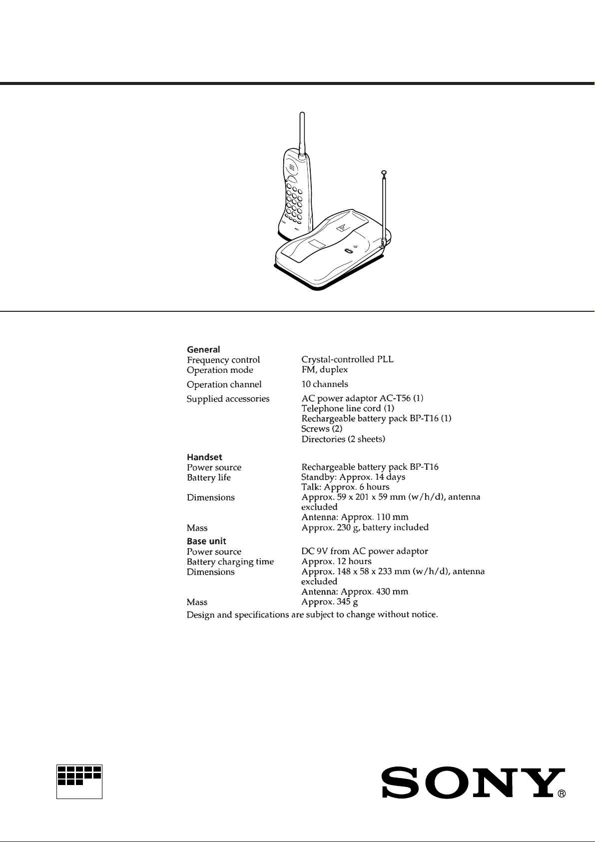
SPECIFICATIONS
E Model
MICROFILM
CORDLESS TELEPHONE
Page 2

TABLE OF CONTENTS
1. SERVICING NOTES ................................................ 3
2. GENERAL
Setting up the phone ....................................................... 4
Making and receiving calls ............................................. 4
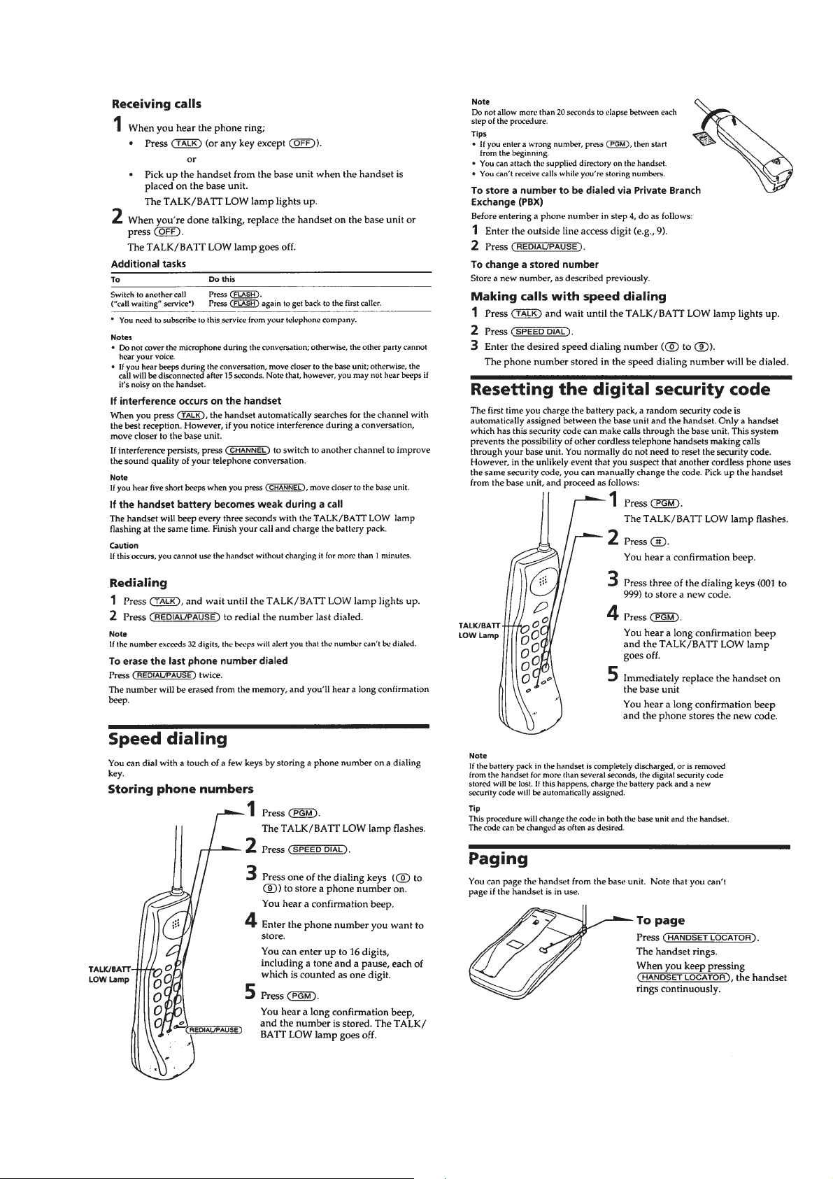
Speed dialing ................................................................... 5
Resetting the digital security code.................................. 5
Paging .............................................................................. 5
3. DISASSEMBLY ......................................................... 6
Flexible Circuit Board Repairing
• Keep the temperature of the soldering iron around 270 ˚C during repairing.
• Do not touch the soldering iron on the same conductor of the
circuit board (within 3 times).
• Be careful not to apply force on the conductor when soldering
or unsoldering.
Notes on chip component replacement
• Never reuse a disconnected chip component.
• Notice that the minus side of a tantalum capacitor may be damaged by heat.
4. TEST MODE
4-1. Base Unit Section............................................................ 8
4-2. Handset Section............................................................... 10
5. ELECTRICAL ADJUSTMENTS
5-1. Base Unit Section............................................................ 13
5-2. Handset Section............................................................... 14
6. DIAGRAMS
6-1. Block Diagram – BASE UNIT Section –...................... 19
6-2. Block Diagram – HANDSET Section –........................ 21
6-3. Notes for Printed Wiring Board and
Schematic Diagram ......................................................... 23
6-4. Printed Wiring Boards – BASE UNIT Section – .......... 25
6-5. Schematic Diagram – BASE UNIT Section –................ 27
6-6. Printed Wiring Board – HANDSET Section –.............. 29
6-7. Schematic Diagram – HANDSET Section –................. 31
6-8. IC Pin Function Description ........................................... 33
7. EXPLODED VIEWS ................................................ 35
8. ELECTRICAL PARTS LIST ............................... 37
SAFETY-RELATED COMPONENT WARNING!!
COMPONENTS IDENTIFIED BY MARK ! OR DOTTED
LINE WITH MARK ! ON THE SCHEMATIC DIA GRAMS
AND IN THE PARTS LIST ARE CRITICAL TO SAFE
OPERATION. REPLACE THESE COMPONENTS WITH
SONY PARTS WHOSE PART NUMBERS APPEAR AS
SHOWN IN THIS MANU AL OR IN SUPPLEMENTS PUBLISHED BY SONY.
– 2 –
Page 3
SECTION 1
SERVICING NOTES
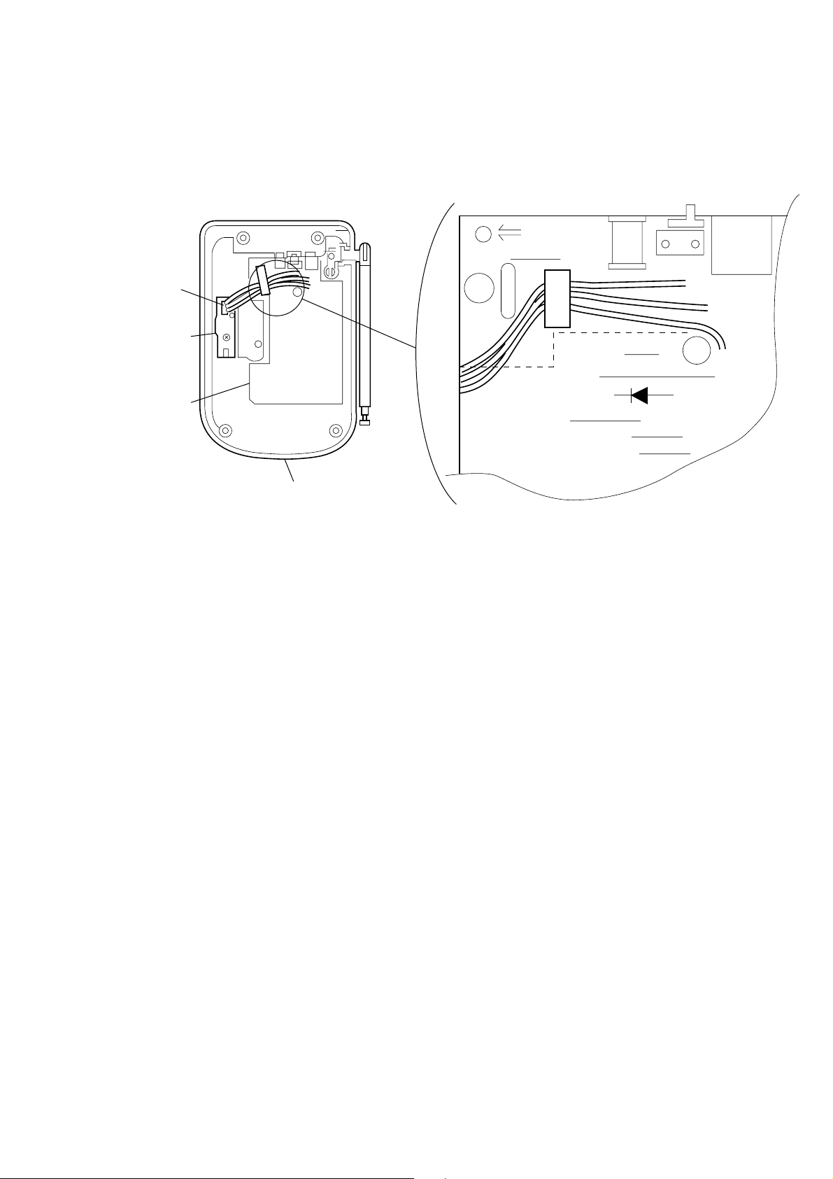
PREVENT ELECTROSTATIC DESTRUCTION
• To prevent electrostatic destruction in replacing the main board, etc., fasten the CN602 cable as shown below.
JW5
CN602
SUB board
BASE MAIN board
cabinet lower
C502
X501
JW12
JW6
JW10
D101
JW7
C303
JW3
– 3 –
Page 4
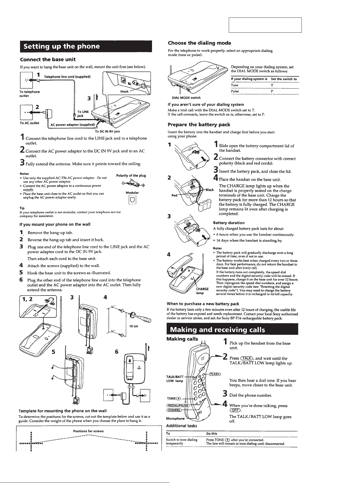
SECTION 2
GENERAL
This section is extracted from
instruction manual.
– 4 –
Page 5
– 5 –
Page 6
SECTION 3
d
y
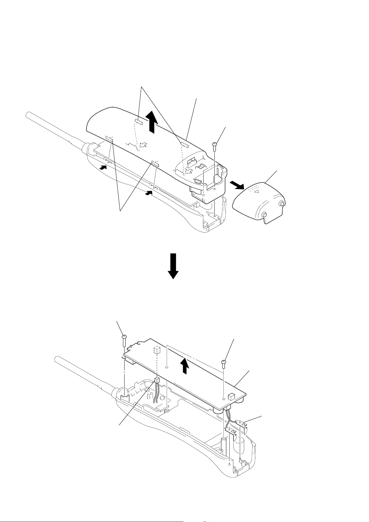
DISASSEMBLY
Note: Follow the disassembly procedure in the numerical order given.
• HANDSET
REAR CABINET
3
two claws
A
4
Removal the rear cabinet to
direction of the arrow
2
two screws
(BTP2.6
A
.
×
8)
1
battery case li
HAND MAIN BOARD
1
screw
(BTP2.6
3
two claws
×
12)
2
two screws
(BTP2.6
×
8)
3
HAND MAIN board
5
connector
(CN101)
– 6 –
4
terminal ass’
(charge)
Page 7
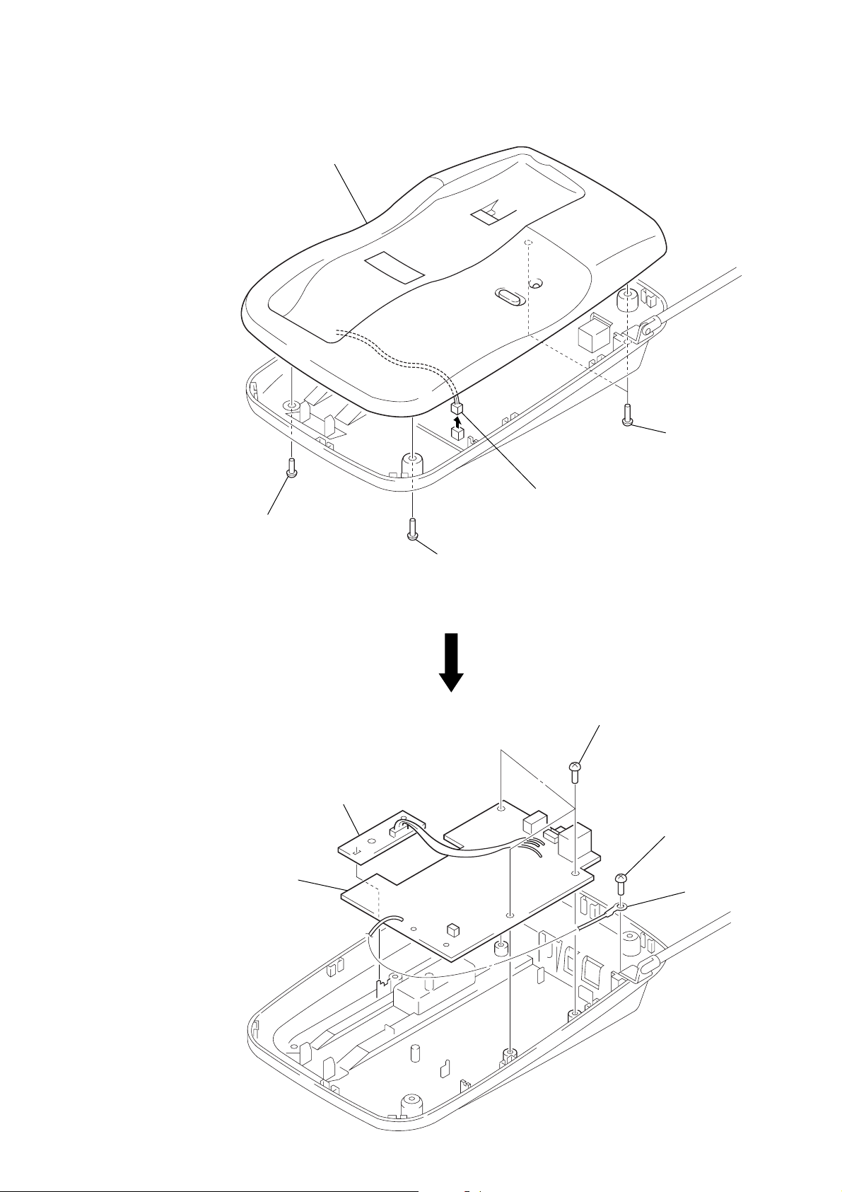
• BASESET
l
BASESET (UPPER) ASS’Y
1
2
baseset (upper) ass’y
screw
(P3
×
10)
1
screw
(P3
×
10)
3
connector
(CN301)
1
two screws
(P3
×
10)
BASE MAIN BOARD
4
BASE MAIN board
4
SUB board
1
three screws
(BTP2.6
×
8)
2
screw
(BTP2.6
3
ring termina
×
8)
– 7 –
Page 8
SECTION 4
)
TEST MODE
4-1. BASE UNIT SECTION
<Enter the Test Mode>
Manual T est Mode
1. Set the [DIALMODE] switch to “P” (pulse).
2. While pressing the [PAGE] key, switch on the power supply
(Reset start).
3. With the [PAGE] key, still held down, switch the [DIALMODE]
switch “P” (pulse) n “T” (tone) n “P” (pulse).
4. When you release the [PAGE] key, test mode starts.
5. Frist dial “0” at 10 pps. Then ouput “1”, “4”, “8” and “#”
with DTMF.
6. Set to TX ON. Goes to external line state in 1 CH.
• Release the Test Mode
1. Pull out the AC adapter and turn off the power.
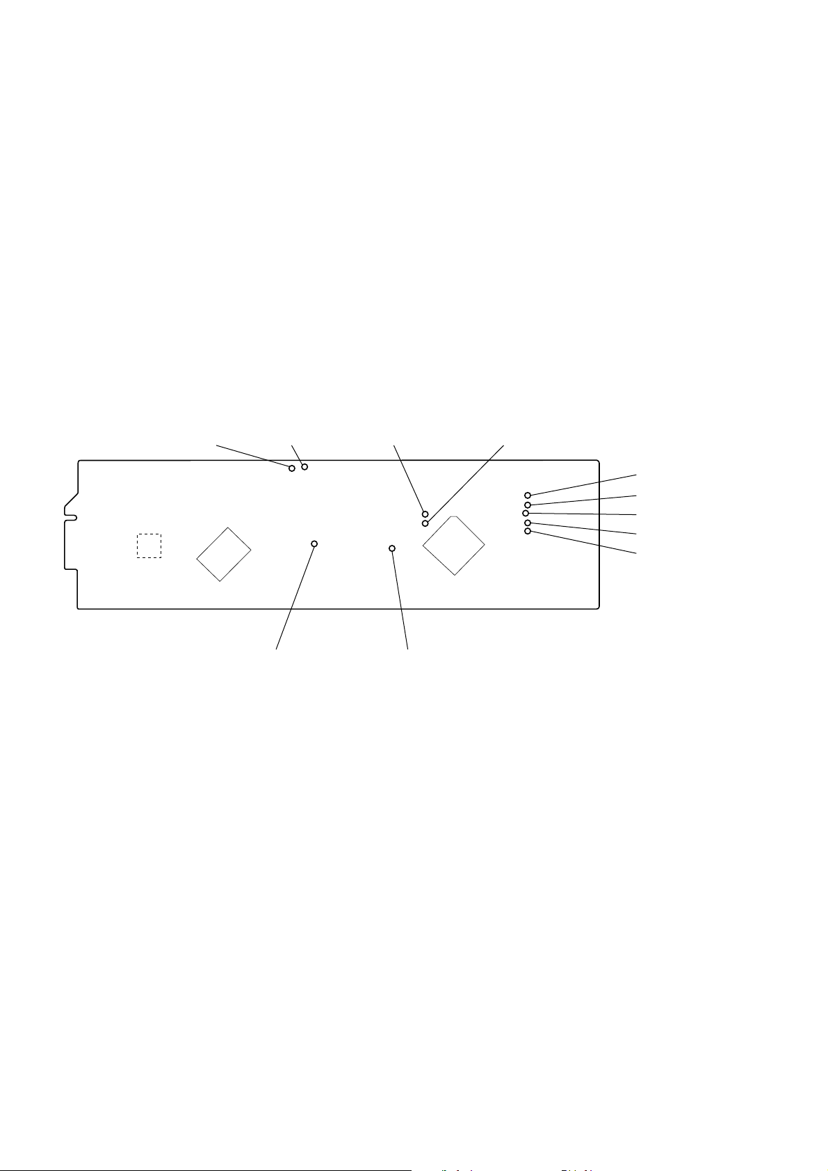
[BASE MAIN Board] (Conductor side)
Machine Test Mode
1. With one of the CH setting terminals in “H” input state, cause
Reset of Power ON. Equipment enters machine test mode.
2. Setting of CH according to logic input with CH setting terminal.
3. ON/OFF of TX is according to the input logic of the Dial Mode
terminal.
• Release the Test Mode
1. Pull out the AC adapter and turn off the power.
2. Remove the short plug and turn on the power again.
TP61 (M1)
TP62 (M2)
TP63 (M3)
TP66 (TEST2)
TP21 (CHG DET)
TP46 (PAGE)
MJ201
TP47 (DIAL MODE
TP106 (5V)
IC501
TP67 (TEST1)
TP64 (M4)
TP65 (TEST3)
IC101
CF101
– 8 –
Page 9
Channel Setting
During startup in machine test mode, make the following channel settings by loading the terminal input data.
Pin No. @£ @¢ @∞ @§ TX Frequency RX Frequency
Channel M1 (TP61) M2 (TP62) M3 (TP63) M4 (TP64) (MHz) (MHz)
CH1 H L L L 43.720 48.760
CH2 L H L L 43.740 48.840
CH3 H H L L 43.820 48.860
CH4 L L H L 43.840 48.920
CH5 43.920 49.020
CH6 43.960 49.080
CH7 44.120 49.100
CH8 44.160 49.160
CH9 44.180 49.200
CH10 44.200 49.240
CH11 44.320 49.280
CH12 44.360 49.360
CH13 44.400 49.400
CH14 H L H L 44.460 49.460
CH15 L H H L 44.480 49.500
CH16 H H H L 46.610 49.670
CH17 L L L H 46.630 49.845
CH18 46.670 49.860
CH19 46.710 49.770
CH20 46.730 49.875
CH21 46.770 49.830
CH22 46.830 49.890
CH23 H L L H 46.870 49.930
CH24 L H L H 46.930 49.990
CH25 H H L H 46.970 49.970
TEST1 L L H H 43.780 48.800
TEST2 H L H H 43.890 48.970
TEST3 L H H H 46.800 49.910
TEST4 H H H H 46.900 49.950
Machine Test Mode Input/Output
1. Input (Input ports for other than main tasks)
Pin Name Pin No. Function Logic
M1 (TP61) @£
M2 (TP62) @¢
M3 (TP63) @∞
M4 (TP64) @§
DIAL MODE (TP47) !¶ Setting the TX ON/OFF H (T); OFF, L (P): ON
PAGE (TP46) !§ Machine: Dial data “5” is output to Key input with “L” input. The first time there is
TEST 1 (TP67) TEST 2 (TP66) TEST 3 (TP65)
@ª @• @¶
L L L If RSSI (H) is, detected: Light ON If RSSI (H) is, detected: Light ON
L L H If RSSI (L) is, detected: Light ON If RSSI (L) is, detected: Light ON
L H L If TX LOCK is detected: Light OFF If TX LOCK is detected: Light OFF
L H H If RX LOCK is detected: Light OFF If RX LOCK is detected: Light OFF
H L L BEEP output
H L H ID CODE output
H H L If RING is detected: Light ON If RING is detected: Light ON
H H H If PAGE KEY is input: Light ON If PAGE KEY is input: Light ON
Setting the CH (channel) Refer to channel setting
Manual: Channel increment Incrementing of channels in order from 16 to 25.
DTMF/DP exchange output of “5” with DTMF.
Operation with CHARGE LED Operation with TX ON
2. Output (Output ports for other than main tasks)
Pin Name Pin No. Function H Logic L Logic
CHARGE DET !• State in section 1. Input Refer to Section 1. Input
– 9 –
Page 10
4-2. HANDSET SECTION
)
)
)
)
)
<Enter the Test Mode>
Manual T est Mode
1. Enter the test mode by pressing [0] key while pressing the [1]
key and [TALK] when in idle condition.
(Key operation: [0] n [1] n [TALK] )
2. The RINGER will ring for 500msec when the test mode is
started.
3. Measurement mode of consumption current. (42# state. Refer
to 2-3)
4. Use key input to carry out the various settings.
5. Use port inputs to set output from LED terminals.
• Release the Test Mode
1. Press the [0], [0] and [#] key.
2. Turn OFF the power. (Remove the battery and replace them)
[HAND MAIN Board] (Conductor side)
L102
IC101
Machine Test Mode
1. When power on reset is applied while a H (high) is input to the
TEST SW (TP43) terminal (IC501 pin $º), the RING (Level
H, 500 msec) sounds.
2. Following that, at a timing in which the TEST SW terminal
has “H” (High) input, there is output of “L” by the CH (Channel) setting control terminal. Then there is PLL setting to the
CH which was read to with the CH setting terminal according
to that “L” output.
3. Set the TX setting to TX OFF.
4. The TX channel is used by voice, not by data.
5. Use port inputs to set output from LED terminals
• Release the Test Mode
1. Turn off the power.
2. Remove the short plug and turn on the power.
TP44 (TEST ACT)TP43 (TEST SW)TP36 (H)TP35 (TALK LED)
TP13 (ROW 5
TP14 (ROW 4
TP15 (ROW 3
IC501
TP16 (ROW 2
TP17 (ROW 1
TP55 (KEY LED)
TP33 (TEST CH)
– 10 –
Page 11

Channel Setting
During startup in machine test mode, make the following channel settings by loading the terminal input data.
Pin No. #¢ #£ #™ #¡ @ª RX Frequency TX Frequency
Channel ROW 5 (TP13) RO W 4 (TP14) ROW 3 (TP15) ROW 2 (TP16) RO W 1 (TP17) (MHz) (MHz)
CH1HLLLL 43.720 48.760
CH2 H L L L H 43.740 48.840
CH3 H L L H L 43.820 48.860
CH4 H L L H H 43.840 48.920
CH5 H L H L L 43.920 49.020
CH6 H L H L H 43.960 49.080
CH7 H L H H L 44.120 49.100
CH8 H L H H H 44.160 49.160
CH9 H H L L L 44.180 49.200
CH10 H H L L H 44.200 49.240
CH11 H H L H L 44.320 49.280
CH12 H H L H H 44.360 49.360
CH13 H H H L L 44.400 49.400
CH14 H H H L H 44.460 49.460
CH15 H H H H L 44.480 49.500
CH16 L L H H L 46.610 49.670
CH17 L L H H H 46.630 49.845
CH18 L H L L L 46.670 49.860
CH19 L H L L H 46.710 49.770
CH20 L H L H L 46.730 49.875
CH21 L H L H H 46.770 49.830
CH22 L H H L L 46.830 49.890
CH23 L H H L H 46.870 49.930
CH24 L H H H L 46.930 49.990
CH25 L H H H H 46.970 49.970
TEST1 L L L H L 43.780 48.800
TEST2 L L L H H 43.890 48.970
TEST3 L L H L L 46.800 49.910
TEST4 L L H L H 46.900 49.950
Machine Test Mode Input/Output
1. Input (Input ports for other than main tasks)
Pin Name Pin No. Function Logic
ROW 1 (TP17) @ª
ROW 2 (TP16) #¡
ROW 3 (TP15) #™ Setting the CH (channel) Refer to channel setting
ROW 4 (TP14) #£
ROW 5 (TP13) #¢
TEST CH (TP33) 1 Control terminal for setting the CH (channel) H: OFF, L: ON
TEST SW (TP43) $º Start up of test mode H: Start, L: No start
TEST ACT (TP44) $¢
During test mode, causes start of intermittent operation
with external input.
H: Intermittent start
2. Output (Output ports for other than main tasks)
Pin Name Pin No. Function H Logic L Logic
TALK LED (TP35) $•
KEY LED (TP55) 2
Various input/output monitor output (default: RSSI(H)
detection).
During test mode: All lights lit, However, does not include
measurement of consumption current.
No detection Detection
No light Light
– 11 –
Page 12

Key processing (Setting the manual test mode)
1. (Upper position) (Lower Position) Set with #.
2. 3X# can be substituted with X
.
Upper
position
Lower
position RF AF
0 QUIT 10ch 20ch Batt Alarm H A L T G KEY TEST
1 1ch 11ch 21ch CHARG DET Gg G G G
2 2ch 12ch 22ch GggGG
3 3ch 13ch 23ch gg G G G
4 4ch 14ch 24ch RX LOCK gggGG
5 5ch 15ch 25ch TX LOCK gg g g G
6 6ch 16ch T1ch RSSI (H) ggggg
7 7ch 17ch T2ch RSSI (L) – – – – –
8 8ch 18ch T3ch DATA TX – – – – –
9 9ch 19ch T4ch – – – – –
Purpose CH setting only
Application
0123 7
SIGOUT General
control operation
The standard is external line communication
state.
State for standard electrical adjustment process.
Condition
suveillance Measurement mode of consumption
with TALK current.
LED.
TX
RX RX
4
MIC Lk
• By pressing the CH key there is increment of the channel. However, this does not include the test channel.
• Control of the power source during 38# DATA TX is (TX&RX
RF&RX AF=ON) in 44# state.
• Control of the power source during the 70# key check mode is
41# state (TX OFF).
• For CH setting, SIGOUT control and power source control (with
the exception of above-mentioned 38# state) the state can be set
independently.
Example: In 15 c h, the order for carrying out TX modulation
level and RSSI (H) sensitivity setting is as follows:
The following are possible:15# n 44# n 36#
36# n 15# n 44#
44# n 36# n 15#
g: ON, G: OFF
Lk: KEY LED
– 12 –
Page 13

SECTION 5
d
d
d
level meter
600
Ω
+
–
PBX tester or
TP105
TP104
BASE MAIN
board
F.B.
DC 48 V
ELECTRICAL ADJUSTMENTS
5-1. BASE UNIT SECTION
• Apply 9 V dc from regulated DC power supply.
• Set to base unit machine test mode. (See page 8)
• Switch position:
SW302 (DIAL MODE): P (pulse)
TX Section Adjustment
• Perform the adjustment at T3CH (28CH: 46.8 MHz) as a rule.
Note: The electrolytic capacitor (10 µF/10 V) connected TP23 (DET) to
GND. (Only TX section adjustment)
BASE MAIN board
TP23 (DET)
10 µF
set
1. TX VT Adjustment
Setting:
digital voltmeter
+
–
+
BASE MAIN boar
TP6 (TX VT)
TP19 (GND)
RX Section Adjustment
1. RX Level Adjustment
• Perform the adjustment at T3CH (28CH: 49.910 MHz) as a rule.
Setting :
FM RF SSG
BASE MAIN boar
TP2
TP3 (RF GND)
Procedure :
1. FM RF SSG condition :
Carrier frequency : 49.910 MHz
Modulation frequency: 1 kHz
Deviation : 3 kHz
Output level : 60 dBµV (1 mV) (EMF)
2. Adjust the FL101 for the maximum reading on the level meter .
Also check that the output level is within the specified values.
Procedure :
1. The digital voltmeter connected TP6 (TX VT) to TP19 (GND).
2. Adjust the L52 for 2.2 ± 0.05 V reading on the digital voltmeter.
Adjustment Location: BASE MAIN board (See page 16)
Specified value: – 2.6 to – 10.6 dBV
Adjustment Location: BASE MAIN board (See page 16)
2. RX VT Adjustment
Setting:
digital voltmeter
BASE MAIN boar
+
–
TP5 (RX VT)
TP19 (GND)
Procedure :
1. The digital voltmeter connected TP5 (RX VT) to TP19 (GND).
2. Adjust the L101 for 2.4 ± 0.05 V reading on the digital voltmeter.
Adjustment Location: BASE MAIN board (See page 16)
– 13 –
Page 14

3. RSSI (H) Sensitivity Adjustment
d
T
d
)
• Perform the adjustment at T3CH (28CH: 49.910 MHz) as a rule.
Setting :
5-2. HANDSET SECTION
• Apply 4 V dc from regulated DC power supply.
• Set to handset machine test mode. (See page 10)
AF ocillator
output: 20 Hz
FM RF SSG
BASE MAIN boar
TP2
TP3 (RF GND)
Procedure :
1. FM RF SSG condition :
Carrier frequency : 49.910 MHz
Modulation frequency: 20 Hz (EXT)
Deviation : AM 50%
Output level : 60 dBµV (1mV) (EMF)
2. Use the oscilloscope to confirm the FM RF SSG input (AF)
signal waveform and RSSI signal, and use the RV101 so that
they are synchronized matched (duty is synchronized).
oscilloscope
(DC range)
BASE MAIN boar
+
–
RSSI WAVEFORM
TP9 (SIG OUT)
TP19
TX Section Adjustment
• Perform the adjustments at T1CH (26CH: 43.780 MHz) as a
rule.
1. TX VT Adjustment
Setting:
digital voltmeter
+
–
Procedure:
1. The digital voltmeter connected TP6 (TX VT) to TP3 (RX
GND).
2. Adjust the L52 for 0.9 V ± 0.05 V reading on the digital
voltmeter.
Adjustment Location: HAND MAIN board (See page 17)
TP6 (TX VT)
TP3 (RX GND
RSSI output waveform
0V
Adjust so that they
synchronize at 0V.
RF signal EX
signal 20Hz
Adjustment Location: BASE MAIN board (See page 16)
– 14 –
Page 15

RX Section Adjustment
d
RSSI WAVEFORM
RSSI output waveform
RF signal EXT
signal 20Hz
0V
Adjust so that they
synchronize at 0V.
)
1. RX Level Adjustment
• Perform the adjustment at T1CH (26CH: 43.780 MHz) as a rule.
Setting :
FM RF SSG
HAND MAIN board
TP2
TP3 (RX GND)
3. RSSI (H) Sensitivity Adjustment
• Perform the adjustment at T1CH (26CH: 43.780 MHz) as a
rule.
Setting :
AF ocillator
output: 20 Hz
FM RF SSG
HAND MAIN board
TP2
TP3 (RX GND)
Procedure :
1. FM RF SSG condition :
Carrier frequency : 43.780 MHz
Modulation : 1 kHz
Deviation : 3 kHz
Output level : 60 dBµV (1 mV) (EMF)
2. Adjust the FL101 for the maximum reading on the level meter .
Also check that the output level is within the specified values.
level meter
HAND MAIN boar
+
–
TP27 (SP)
TP26 (SP)
Specified value: –16.6 to –8.6 dBV
Adjustment Location: HAND MAIN board (See page 17)
2. RX VT Adjustment
Setting:
digital voltmeter
+
–
TP5 (RX VT)
TP3 (RX GND
Procedure:
1. The digital voltmeter connected TP5 (RX VT) to TP3 (RX
GND).
2. Adjust the L102 for 0.8 V ± 0.05 V reading on the digital
voltmeter.
Procedure :
1. FM RF SSG condition :
Carrier frequency : 43.780 MHz
Modulation frequency : 20 Hz (EXT)
Deviation : AM 50%
Output level : 2 dBµV (1.259 µV) (EMF)
2. Use the oscilloscope to confirm the FM RF SSG input (AF)
signal waveform and RSSI signal, and use the RV101 so that
they are synchronized matched (duty is synchronized).
oscilloscope
(DC range)
HAND MAIN board
+
–
TP9 (SIG IN)
TP3 (RX GND)
Adjustment Location: HAND MAIN board (See page 17)
Adjustment Location: HAND MAIN board (See page 17)
– 15 –
Page 16

Adjustment Location :
t
[BASE MAIN Board] (Component Side)
FL101 RX Level Adjustment
L101 RX VT Adjustment
L52 TX VT Adjustment
[BASE MAIN Board] (Conductor Side)
TP2
TP3 (RF GND)
RV101 RSSI (H) Sensitivity Adjustmen
TP5
(RX VT)
TP6 (TX VT)
IC101
TP9 (SIG OUT)
IC501
CF101
TP19 (GND)
TP105
TP104
MJ201
– 16 –
Page 17

Adjustment Location :
[HAND MAIN Board] (Component Side)
L102 RX VT Adjustment
FL101 RX Level Adjustment
[HAND MAIN Board] (Conductor Side)
TP26 (SP)
TP27 (SP)
TP3 (RX GND)
TP2
RV101 RSSI (H) Sensitivity Adjustment
L52 TX VT Adjustment
L102
TP5
(RX VT)
IC101
TP6 (TX VT)
IC501
TP9
(SIGIN)
– 17 –
Page 18

SECTION 6
DIAGRAMS
6-1. BLOCK DIAGRAM – BASE UNIT Section –
MIX, IF AMP, LIMITER AMP,
ANT1
TELESCOPIC
ANTENNA
RX FREQUENCY:
49.67 – 49.99MHz
B.P.F.
TX FREQUENCY:
46.61 – 46.97MHz
B.P.F.
BPF51
BPF1
(RX VCO)
RX SYSTEM B+
RF AMP
Q1
L101
RX VT
TX AMP
Q51
B.P.F.
BPF2
43
44
42
46
41
L52
(TX VCO)
TX VT
PLL, EXPANDER/COMPRESSOR
LO OUT
LO IN
CONTR
PD OUT
VCC2
TX VCO
Q52
IC101 (1/2)
MIX1
IN1
40
IC101
1ST
MIX
RX
VCO
RX
PLL
MODULATOR
MIX1
D51
OUT
38
10.68MHz
9
47
CF102
FIL OUT
PD
OUT
SPP-68
D205
RECT
HOOK ON/OFF
SWITCH
PH202
HOOK ON/OFF
Q201
• SIGNAL PATH
: RX
: TX
: BELL
RINGER
DETECT
PH201
MJ201
LINE
FL101
(DET)
RX LEVEL
28
MIX2
MIX2
IN
36
2ND
MIX
LOCAL
OSCILLATOR
TX
SPLATTER
TX
PLL
OUT
CF101
460kHz
34
LO1
LO2
FIL IN
3
4
IF
IN
32
X101
10.22MHz
AMP
IF
11
QUADRATURE
DETECTOR
RSSI
COMP
OUT
QUAD
TX
MUTE
CARRIER
DETECTOR
AF
OUT
L.P.F.
SIG
OUT
RSSI
H/L
COMPRESSOR/
LIMITER
27
22
RV101
RSSI (H)
SENSITIVITY
MIC
IN
MIC AMP
1410
IC101 (2/2)
PRE
IN
15
COMP
IN
24
PREAMP
DATA
COMP
EXPANDER
DA OUT
23
CPU
INTERFACE
DATA
CLK
CLK
DATA
LATCH
8567
LATCH
RX
MUTE
EXP
OUT
AMP
SIDE TONE
CANCEL
AMP
OUT
AMP
OUT
19
20
T201
LINE TRANSFORMER
+
LINE TX
DRIVE
Q203
SWITCH CONTROL
AMP
IN
17
+
D101
RECEIVER
18
TEL AMP
Q202
TVCOIN
1
X501
4.048MHz
10
9
OSC1
OSC2
PAGE
16
05
S301
PAGE
DIALMODE
17 12
SW302
DIAL MODE
T
P
7
TX-DATA
SYSTEM CONTROLLER
IC501
19
RSSI H/L
5
SIG-IN
6
H-MUTE
CLK
DATA
LATCH
2
3
CHG-DET
TX +B CTRL
DATA
CLK
RESET
1
STB
RESET
SWITCH
Q302
TX SYSTEM B+
B+
21
POW-DET
DTMF
VOLTAGE
DETECT
IC301
B+ SWITCH
Q54
REGULATOR
Q301
REGULATOR
Q601
4 20
RX-DATA
18 22 14
DP
–
30
RING
J301
DC IN 9V
+
D401
POWER
CHARGE/IN USE
– 19 – – 20 –
REGULATOR
CHARGE DETECT
Q401
CHARGE
Q402
CURRENT
LIMITER
Q403
+
CHARGE
TERMINAL
–
Page 19

SPP-68
6-2. BLOCK DIAGRAM – HANDSET Section –
MIX, IF AMP, LIMITER AMP,
ANT2
RX FREQUENCY:
46.61 – 46.97MHz
B.P.F.
TX FREQUENCY:
49.67 – 49.99MHz
RX SYSTEM B+
B.P.F.
BPF51
BPF1
L102
(RX VCO)
RX VT
RF AMP
Q1
D101
TX AMP
Q51
B.P.F.
BPF2
43
44
42
46
41
L52
(TX VCO)
TX VT
PLL, EXPANDER/COMPRESSOR
LO OUT
LO IN
CONTR
PD OUT
VCC2
TX VCO
Q52
IC101 (1/2)
MIX1
IN1
40
IC101
1ST
MIX
RX
VCO
RX
PLL
MODULATOR
D51
MIX1
OUT
38
CF102
10.66MHz
FIL OUT
9
PD
OUT
47
TVCOIN
1
FL101
(DET)
RX LEVEL
• SIGNAL PATH
: RX
: TX
: BELL
28
MIX2
MIX2
IN
36
2ND
MIX
LOCAL
OSCILLATOR
TX
SPLATTER
TX
PLL
OUT
CF101
460kHz
34
LO1
LO2
FIL IN
3
4
IF
IN
32
X101
10.22MHz
AMP
IF
11
QUADRATURE
DETECTOR
RSSI
COMP
OUT
QUAD
TX
MUTE
CARRIER
DETECTOR
AF
OUT
L.P.F.
SIG
OUT
RSSI
H/L
COMPRESSOR/
LIMITER
27
22
MIC AMP
RV101
RSSI (H)
SENSITIVITY
MIC
IN
1410
MIC1
IC101 (2/2)
PRE
IN
15
COMP
IN
24
PREAMP
DATA
COMP
EXPANDER
DA OUT
23
CPU
INTERFACE
DATA
CLK
CLK
DATA
LATCH
8567
LATCH
RX
MUTE
EXP
OUT
AMP
BATTERY
DETECT
BATTERY LOW
SWITCHING
Q502
AMP
OUT
AMP
OUT
BATT
19
20
IN
33
SP1
B+
BUZZER
DRIVE
Q301
BZ301
(BUZZER)
AMP
IN
17
RECEIVER
18
DET
OUT
21
B+
X501
4.048MHz
MIC
45
3 37
46
SIG-IN
H-MUTE
RSSI H/L
TX +B CTRL
13
HOLD/RESET
SWITCH
Q501
HOLD
12
B+
17
20
OSC1
OSC2
48
D501
TALK/
BATT LOW
05
LED
9
10
TX-DATA
TX-DATA
SYSTEM CONTROLLER
ROW1 – ROW5
29, 31 – 34
KEY MATRIX
(SEET KEY)
IC501
COL0 – COL3
24 – 27
COL3
28
8
RX-DATA
DATA
5
PLL-DATA
D502
CLK
7
PLL-CLK
D504
LATCH
4
PLL-STB
22
ACT3
RESET
21
MAIN
GROUND
TX SYSTEM B+
23
ACT4
BATT-LOW
RESET
SWITCH
Q201
GROUND ISOLATION
SWITCHING
B+
Q202
B+ SWITCH
Q54
VOLTAGE
DETECT
IC201
POWER
GROUND
11
BEEP
47
BATT-DET
D202
CHG-DET
38
+
CHARGE
TERMINAL
–
BT901
RECHARGEABLE
BATTERY PACK
(BP-T16)
– 21 – – 22 –
Page 20

6-3. NOTES FOR PRINTED WIRING BOARD AND SCHEMATIC DIAGRAM
Note on Schematic Diagram:
• All capacitors are in µF unless otherwise noted. pF: µµF
50 WV or less are not indicated except for electrolytics
and tantalums.
• All resistors are in Ω and 1/
specified.
¢
•
• C : panel designation.
• U : B+ Line.
• H : adjustment for repair.
• Power voltage is dc 9 V and fed with regulated dc power
• Power voltage is dc 12 V and fed with regulated dc power
• Power voltage is dc 3.6 V and fed with regulated dc power
• Voltages and wav eforms are dc with respect to ground in
• Voltages are taken with a VOM (Input impedance 10 M Ω).
• Waveforms are taken with a oscilloscope.
• Circled numbers refer to waveforms.
• Signal path.
: internal component.
supply from external power voltage jack (J301 on the
BASE MAIN board).
supply from modular jack (MJ201 on the BASE MAIN
board) with 100 Ω in series.
supply from battery jack (CN201 on the HAND MAIN
board).
test mode.
Voltage variations may be noted due to normal production tolerances.
Voltage variations may be noted due to normal production tolerances.
N : RX
O : TX
P : bell
: Impossible to measure
∗
4
W or less unless otherwise
Note on Printed Wiring Boards:
• X : parts extracted from the component side.
• Y : parts extracted from the conductor side.
¢
•
• b : Pattern from the side which enables seeing.
(The other layers' patterns are not indicated.)
Caution:
Pattern face side: Parts on the pattern face side seen from
(Conductor Side) the pattern face are indicated.
Parts face side: Parts on the parts face side seen from
(Component Side) the parts face are indicated.
: internal component.
• Waveforms
– BASE MAIN Board –
1 IC101 3 (Test Mode)
1.4 Vp-p
97.8 ns
2 IC501 9 (OSC2) (Tset Mode)
3.1 Vp-p
247 ns
– HAND MAIN Board –
1 IC101 3 (Test Mode)
97.8 ns
2 IC501 @º (OSC2) (Tset Mode)
247 ns
680 mVp-p
3.6 Vp-p
– 23 –
– 24 –
Page 21

SPP-68
6-4. PRINTED WIRING BOARDS – BASE UNIT Section –
• Semiconductor
Location
Ref. No. Location
D1 H-3
D51 I-7
D101 C-4
D201 B-2
D203 C-2
D204 C-2
D205 C-1
D301 C-3
D401 E-2
D501 D-7
D602 C-3
IC101 F-5
IC301 A-7
IC501 B-6
PH201 C-3
PH202 D-2
Q1 H-3
Q51 I-5
Q52 I-6
Q54 I-5
Q201 E-2
Q202 D-4
Q203 D-1
Q301 C-4
Q302 A-6
Q401 I-1
Q402 F-2
Q403 F-2
– 25 – – 26 –
Page 22

6-5. SCHEMATIC DIAGRAM – BASE UNIT Section – • See page 24 for Waveforms.
SPP-68
– 27 – – 28 –
Page 23

SPP-68
6-6. PRINTED WIRING BOARD – HANDSET Section –
• Semiconductor Location
(Conductor Side)
Ref. No. Location
D51 A-3
D101 C-3
D202 B-13
D301 A-13
D501 D-6
D502 A-10
D504 A-11
IC101 B-4
IC201 D-13
IC501 B-10
Ref. No. Location
Q1 C-2
Q51 A-1
Q52 A-2
Q54 B-1
Q201 D-9
Q202 C-13
Q301 A-13
Q501 C-8
Q502 C-8
– 29 – – 30 –
Page 24

6-7. SCHEMATIC DIAGRAM – HANDSET Section – • See page 24 for Waveforms.
SPP-68
– 31 – – 32 –
Page 25

6-8. IC PIN FUNCTION DESCRIPTION
• BASE MAIN BOARD IC501 SB662106A-4J90-TLM (SYSTEM CONTROLLER)
Pin No. Pin Name I/O Function
1 STB O PLL serial data latch pulse signal output to the TB31223F (IC101)
2 DATA O PLL serial data output to the TB31223F (IC101)
3 CLK O
4 RX-DATA I
5 SIG-IN I
6 H-MUTE O
7 TX-DATA O Transmit data output terminal
8 VSS —
9 OSC2 O
10 OSC1 I
11 VDD —
12 RESET I
13 TEST I
14 POW-DET I
15 MBR I
16 PAGE I
17 DIALMODE I
18 CHG-DET I
19 RSSI H/L O
20 DP O
21 DTMF O
22 TX +B CTRL O Power on/off control signal output of the transmit system “L”: power on
23 to 26 M1 to M4 I
27 TEST3 I
28 TEST2 I
29 TEST1 I
30 RING I
PLL serial data transfer clock signal output to the TB31223F (IC101)
Receive data input from the TB31223F (IC101)
Squelch signal (carrier detection signal) input from the TB31223F (IC101)
“L”: carrier present, “H”: no carrier
Halt muting on/off control signal output for the receiving data “L”: muting on
Ground terminal
Main system clock output terminal (4.048 MHz)
Main system clock input terminal (4.048 MHz)
Power supply terminal (+5V)
System reset signal input from the reset signal generator (Q302 and IC301) “L”: reset
For several hundreds msec. after the power supply rises, “L” is input, then it changes to “H”
Test terminal (fixed at “L”)
Power down detection signal input from the voltage detector (IC301) “L”: power down
Setting terminal for the make 30% or 40% select “L”: 40%, “H”: 30%
Fixed at “H” in this set
PAGE switch (S301) input terminal When key pressing: “L”
Detect signal input of the should dial in pulse mode or tone mode “L”: pulse, “H”: tone
Charge on/off detection signal input terminal “L”: charge on
RSSI sensitivity H/L selection signal output to the TB31223F (IC101) “L”: low sensitivity
Hook on/off control signal output terminal “H”: hook on
DTMF tone signal output terminal
Channel setting terminal for the test mode Normally: fixed at “L”
Setting terminal for the test mode-3
Setting terminal for the test mode-2
Setting terminal for the test mode-1
Detect signal input of the ringer coming “L”: ringer coming
• HAND MAIN BOARD IC501 SH66358C-4J91 (SYSTEM CONTROLLER)
Pin No. Pin Name I/O Function
1 TEST CH O
2 KEY LED O
3 SIG-IN I
4 PLL-STB O PLL serial data latch pulse signal output to the TB31223F (IC101)
5 PLL-DATA O PLL serial data output to the TB31223F (IC101)
6NCO
7 PLL-CLK O
8 RX-DATA I
9, 10 TX-DATA O Transmit data output terminal
11 BEEP O
12 HOLD I
13 TX +B CTRL O
14 RX +B CTRL O
15 TEST I
16 VSS —
17 OSC1 I
18, 19 NC O
20 OSC2 O
21 RESET I
22 ACT3 O
23 ACT4 O
24 to 27 COL0 to COL3 I
28 MIC O
29 ROW1 O
30 NC O
31 to 34 ROW2 to ROW5 O
35, 36 NC O
37 BATT-LOW I
38 CHG-DET I
39 VDD —
40 TEST SW I
41 — I
42, 43 NC O
44 TEST ACT I
45 RSSI H/L O
46 H-MUTE O
47 BATT-DET I
48 LED O
Test mode channel control output terminal “H” active
LED drive signal output of the key illumination LED “L”: LED on Not used (open)
Squelch signal (carrier detection signal) input from the TB31223F (IC101)
“L”: carrier present, “H”: no carrier
Not used (open)
PLL serial data transfer clock signal output to the TB31223F (IC101)
Receive data input from the TB31223F (IC101)
Buzzer drive signal output terminal
Hold control signal input terminal “L”: hold Used for the released standby
Power on/off control signal output of the transmit system “L”: power on
Power on/off control signal output of the receiver system “L”: power on Not used (open)
Test terminal (fixed at “L”)
Ground terminal
Main system clock input terminal (4.048 MHz)
Not used (open)
Main system clock output terminal (4.048 MHz)
System reset signal input from the reset signal generator (Q201 and IC201) “L”: reset
For several hundreds msec. after the power supply rises, “L” is input, then it changes to “H”
Intermittent reception activation control output terminal “L” active
Intermittent reception activation control output terminal “L” active
Key return signal input from the key matrix When key pressing: “L”
Microphone bias control signal output terminal
Key send signal output to the key matrix
Not used (open)
Key send signal output to the key matrix
Not used (open)
Battery voltage detection signal input from the TB31223F (IC101) “L”: power down
Charge on/off detection signal input terminal “H”: charge on
Power supply terminal (+3.6V)
Start-up of the test mode “L”: no start, “H”: start Normally: fixed at “L”
Not used (fixed at “L”)
Not used (open)
During test mode, causes start of intermittent operation with external input
“H”: intermittent start Normally: fixed at “L”
RSSI sensitivity H/L selection signal output to the TB31223F (IC101) “L”: low sensitivity
Halt muting on/off control signal output for the receiving data “L”: muting on
Power down detection input terminal “L”: power down
LED drive signal output of the TALK/BATT LOW LED (D501) “L”: LED on
– 33 –
– 34 –
Page 26

SECTION 7
EXPLODED VIEWS
NOTE:
• -XX and -X mean standardized parts, so they
may have some difference from the original
one.
• Color Indication of Appearance Parts
Example:
KNOB, BALANCE (WHITE) . . . (RED)
↑↑
Parts Color Cabinet's Color
(1) HANDSET SECTION
ANT2
SP1
• Items marked “*” are not stocked since they
are seldom required for routine service. Some
delay should be anticipated when ordering
these items.
6
5
4
#1
• The mechanical parts with no reference number in the exploded views are not supplied.
• Hardware (# mark) list and accessories and
packing materials are given in the last of the
electrical parts list.
7
#2
#1
3
11
2
13
14
1
Ref. No. Part No. Description Remark
1 3-935-513-01 CABINET (FRONT)
2 3-939-071-01 SPONGE (MICROPHONE)
* 3 3-935-522-01 CUSHION (SP) (2)
* 4 3-935-516-03 HOLDER (SPEAKER)
5 3-939-070-01 TERMINAL, ANTENNA
#1
8
12
10
Ref. No. Part No. Description Remark
9 3-370-982-01 FOOT (H) (TWN), RUBBER
10 3-935-520-01 CUSHION (BATTERY)
11 3-935-518-01 CUSHION (MICROPHONE)
12 3-935-517-01 TERMINAL ASSY, CHARGE
13 1-762-664-11 SWITCH, RUBBER KEY
9
* 6 A-3672-609-A HAND MAIN BOARD, COMPLETE
7 3-935-514-01 CABINET (REAR)
8 3-935-515-01 LID, BATTERY CASE
* 14 3-935-519-11 CUSHION (BUZZER)
ANT2 1-501-839-11 ANTENNA (HANDSET)
SP1 1-505-333-11 SPEAKER (2.1cm)
– 35 –
Page 27

(2) BASESET SECTION
59
52
58
#1
#1
54
53
55
Sub board
(included in
56
(including sub board)
56
)
ANT1
#1
#1
not
supplied
51
Ref. No. Part No. Description Remark
51 3-936-691-01 CABINET (LOWER)
52 3-936-695-01 TERMINAL (CHARGE)
53 3-027-558-21 CABINET (UPPER)
54 3-936-692-01 BUTTON (PAGE)
55 3-936-693-01 LENS
#3
#3
57
Ref. No. Part No. Description Remark
* 56 A-3672-611-A BASE MAIN BOARD, COMPLETE
57 3-936-696-21 FOOT, RUBBER
58 3-007-173-01 LABEL (TERMINAL CAUTION) (/S)
59 3-936-694-01 CLAW (WALL HOOK)
ANT1 1-501-511-11 ANTENNA, TELESCOPIC (BASESET)
– 36 –
Page 28

SECTION 8
ELECTRICAL PARTS LIST
BASE MAIN
NOTE:
• Due to standardization, replacements in the
parts list may be different from the parts specified in the diagrams or the components used
on the set.
• -XX and -X mean standardized parts, so they
may have some difference from the original
one.
• RESISTORS
All resistors are in ohms.
METAL: Metal-film resistor.
METAL OXIDE: Metal oxide-film resistor.
F: nonflammable
Ref. No. Part No. Description Remark Ref. No. Part No. Description Remark
* A-3672-611-A BASE MAIN BOARD, COMPLETE
**************************
< BAND PASS FILTER >
BPF1 1-239-916-11 FILTER, BAND PASS
BPF2 1-233-692-11 FILTER, BAND PASS
BPF51 1-239-918-11 FILTER, BAND PASS
< CAPACITOR >
C2 1-163-031-11 CERAMIC CHIP 0.01MF 50V
C3 1-163-037-11 CERAMIC CHIP 0.022uF 10% 25V
C7 1-163-021-11 CERAMIC CHIP 0.01uF 10% 50V
C51 1-163-009-11 CERAMIC CHIP 0.001uF 10% 50V
C52 1-163-037-11 CERAMIC CHIP 0.022uF 10% 25V
C53 1-163-021-11 CERAMIC CHIP 0.01uF 10% 50V
C54 1-163-009-11 CERAMIC CHIP 0.001uF 10% 50V
C55 1-163-113-00 CERAMIC CHIP 68PF 5% 50V
C56 1-163-033-00 CERAMIC CHIP 0.022uF 50V
C57 1-163-235-11 CERAMIC CHIP 22PF 5% 50V
C58 1-163-235-11 CERAMIC CHIP 22PF 5% 50V
C59 1-163-227-11 CERAMIC CHIP 10PF 0.5PF 50V
C60 1-163-227-11 CERAMIC CHIP 10PF 0.5PF 50V
C61 1-163-231-11 CERAMIC CHIP 15PF 5% 50V
C62 1-163-251-11 CERAMIC CHIP 100PF 5% 50V
C63 1-162-587-11 CERAMIC CHIP 0.039uF 10% 25V
C64 1-164-004-11 CERAMIC CHIP 0.1uF 10% 25V
C65 1-164-337-11 CERAMIC CHIP 2.2uF 16V
C66 1-163-021-11 CERAMIC CHIP 0.01uF 10% 50V
C67 1-163-037-11 CERAMIC CHIP 0.022uF 10% 25V
C68 1-163-031-11 CERAMIC CHIP 0.01uF 50V
C69 1-163-009-11 CERAMIC CHIP 0.001uF 10% 50V
C70 1-163-099-00 CERAMIC CHIP 18PF 5% 50V
C71 1-163-224-11 CERAMIC CHIP 7PF 0.25PF 50V
C101 1-165-319-11 CERAMIC CHIP 0.1uF 50V
C102 1-163-239-11 CERAMIC CHIP 33PF 5% 50V
C103 1-163-106-00 CERAMIC CHIP 36PF 5% 50V
C105 1-163-243-11 CERAMIC CHIP 47PF 5% 50V
C106 1-163-137-00 CERAMIC CHIP 680PF 5% 50V
C107 1-165-319-11 CERAMIC CHIP 0.1uF 50V
C108 1-126-964-11 ELECT 10uF 20% 50V
C109 1-163-021-11 CERAMIC CHIP 0.01uF 10% 50V
C110 1-163-035-00 CERAMIC CHIP 0.047uF 50V
C111 1-164-161-11 CERAMIC CHIP 0.0022uF 10% 100V
• Items marked “*” are not stocked since they
are seldom required for routine service.
Some delay should be anticipated when ordering these items.
• SEMICONDUCTORS
In each case, u: µ, for example:
uA. . : µA. . uPA. . : µPA. .
uPB. . : µPB. . uPC. . : µPC. .
uPD. . : µPD. .
• CAPACITORS
uF: µF
• COILS
uH: µH
C112 1-163-037-11 CERAMIC CHIP 0.022uF 10% 25V
(Including SUB BOARD)
C113 1-163-009-11 CERAMIC CHIP 0.001uF 10% 50V
C114 1-163-809-11 CERAMIC CHIP 0.047uF 10% 25V
C115 1-163-021-11 CERAMIC CHIP 0.01uF 10% 50V
C116 1-163-021-11 CERAMIC CHIP 0.01uF 10% 50V
C117 1-163-989-11 CERAMIC CHIP 0.033uF 10% 25V
C118 1-163-021-11 CERAMIC CHIP 0.01uF 10% 50V
C122 1-163-235-11 CERAMIC CHIP 22PF 5% 50V
C123 1-165-319-11 CERAMIC CHIP 0.1uF 50V
C125 1-163-077-00 CERAMIC CHIP 0.1uF 10% 25V
C127 1-163-033-00 CERAMIC CHIP 0.022uF 50V
C128 1-126-964-11 ELECT 10uF 20% 50V
C129 1-163-031-11 CERAMIC CHIP 0.01uF 50V
C130 1-126-791-11 ELECT 10uF 20% 16V
C131 1-165-319-11 CERAMIC CHIP 0.1uF 50V
C133 1-163-241-11 CERAMIC CHIP 39PF 5% 50V
C134 1-126-791-11 ELECT 10uF 20% 16V
C135 1-163-031-11 CERAMIC CHIP 0.01uF 50V
C136 1-163-035-00 CERAMIC CHIP 0.047uF 50V
C137 1-126-791-11 ELECT 10uF 20% 16V
C138 1-165-319-11 CERAMIC CHIP 0.1uF 50V
C201 1-136-193-11 FILM 0.47uF 10% 250V
C202 1-104-664-11 ELECT 47uF 20% 16V
C204 1-164-346-11 CERAMIC CHIP 1uF 16V
C205 1-163-019-00 CERAMIC CHIP 0.0068uF 10% 50V
C206 1-163-031-11 CERAMIC CHIP 0.01uF 50V
C209 1-163-037-11 CERAMIC CHIP 0.022uF 10% 25V
C210 1-126-960-11 ELECT 1uF 20% 50V
C211 1-163-034-00 CERAMIC CHIP 0.033uF 50V
C212 1-126-961-11 ELECT 2.2uF 20% 50V
C213 1-126-961-11 ELECT 2.2uF 20% 50V
C301 1-163-033-00 CERAMIC CHIP 0.022uF 50V
C303 1-126-964-11 ELECT 10uF 20% 50V
C304 1-164-336-11 CERAMIC CHIP 0.33uF 25V
C305 1-163-033-00 CERAMIC CHIP 0.022uF 50V
C306 1-163-033-00 CERAMIC CHIP 0.022uF 50V
C401 1-163-031-11 CERAMIC CHIP 0.01uF 50V
C502 1-126-934-11 ELECT 220uF 20% 10V
C503 1-163-031-11 CERAMIC CHIP 0.01uF 50V
C504 1-163-104-00 CERAMIC CHIP 30PF 5% 50V
C505 1-163-137-00 CERAMIC CHIP 680PF 5% 50V
C506 1-163-104-00 CERAMIC CHIP 30PF 5% 50V
C604 1-163-033-00 CERAMIC CHIP 0.022uF 50V
The components identified by
mark ! or dotted line with mark
! are critical for safety.
Replace only with part number
specified.
When indicating parts by reference
number, please include the board.
– 37 –
Page 29

BASE MAIN
Ref. No. Part No. Description Remark
< FILTER >
CF101 1-760-418-11 FILTER, CERAMIC (460kHz)
CF102 1-767-129-81 FILTER, CERAMIC (10.68MHz)
< CONNECTOR >
* CN301 1-506-984-11 PIN, CONNECTOR (PC BOARD) 2P
* CN602 1-506-985-11 PIN, CONNECTOR (PC BOARD) 3P
< DIODE >
D1 8-719-991-33 DIODE 1SS133T-77
D51 8-719-055-14 DIODE KV1832CTR3
D101 8-719-991-33 DIODE 1SS133T-77
D201 8-719-991-33 DIODE 1SS133T-77
D203 8-719-109-89 DIODE RD5.6ESB2
D204 8-719-109-89 DIODE RD5.6ESB2
D205 8-719-820-97 DIODE U05G4B48
D301 8-719-109-97 DIODE RD6.8ES-B2
D401 8-719-059-87 LED SLR-342VRTB7
(POWER CHARGE/IN USE)
D501 8-719-991-33 DIODE 1SS133T-77
D602 8-719-109-89 DIODE RD5.6ESB2
< FILTER >
FL101 1-409-671-11 COIL, IFT
< IC >
Ref. No. Part No. Description Remark
< COIL >
L1 1-414-108-11 INDUCTOR 0.68uH
L51 1-408-958-21 INDUCTOR 1uH
L52 1-411-884-11 COIL, OSC
L101 1-409-798-11 COIL, OSC
L501 1-408-958-21 INDUCTOR 1uH
< MODULAR JACK >
MJ201 1-766-250-11 JACK, MODULAR (2C) 6P (LINE)
< PHOTO COUPTER >
PH201 8-719-156-73 PHOTO COUPLER PS2501-1LA
PH202 8-719-024-09 PHOTO COUPLER PS2532-1
< TRANSISTOR >
Q1 8-729-031-85 TRANSISTOR 2SC4365-34-TB
Q51 8-729-031-85 TRANSISTOR 2SC4365-34-TB
Q52 8-729-031-86 TRANSISTOR 2SC3142-J3J4-TB
Q54 8-729-026-49 TRANSISTOR 2SA1037AK-T146-R
Q201 8-729-120-28 TRANSISTOR 2SC1623-L5L6
Q202 8-729-106-68 TRANSISTOR 2SD1615A-GP
Q203 8-729-032-66 TRANSISTOR 2SC5069-TD
Q301 8-729-106-68 TRANSISTOR 2SD1615A-GP
Q302 8-729-120-28 TRANSISTOR 2SC1623-L5L6
Q401 8-729-120-28 TRANSISTOR 2SC1623-L5L6
Q402 8-729-106-68 TRANSISTOR 2SD1615A-GP
Q403 8-729-120-28 TRANSISTOR 2SC1623-L5L6
IC101 8-759-361-65 IC TB31223F
IC301 8-759-273-93 IC S-80740AL-A4-T1
IC501 8-759-487-52 IC SB662106A-4J90-TLM
< JACK >
J301 1-778-380-11 JACK, DC (POLARITY UNIFIED TYPE)
< SHORT >
JR1 1-216-295-00 SHORT 0
JR2 1-216-295-00 SHORT 0
JR3 1-216-296-00 SHORT 0
JR4 1-216-295-00 SHORT 0
JR5 1-216-296-00 SHORT 0
JR7 1-216-296-00 SHORT 0
JR8 1-216-296-00 SHORT 0
JR9 1-216-296-00 SHORT 0
JR10 1-216-295-00 SHORT 0
JR11 1-216-295-00 SHORT 0
JR12 1-216-296-00 SHORT 0
JR15 1-216-295-00 SHORT 0
JR16 1-216-295-00 SHORT 0
JR17 1-216-296-00 SHORT 0
JR18 1-216-296-00 SHORT 0
JR19 1-216-296-00 SHORT 0
JR20 1-216-295-00 SHORT 0
JR21 1-216-295-00 SHORT 0
JR22 1-216-295-00 SHORT 0
< RESISTOR >
R1 1-216-061-00 METAL CHIP 3.3K 5% 1/10W
R2 1-216-019-00 METAL CHIP 56 5% 1/10W
R3 1-216-025-00 RES, CHIP 100 5% 1/10W
R4 1-216-037-00 METAL CHIP 330 5% 1/10W
R51 1-216-057-00 METAL CHIP 2.2K 5% 1/10W
(DC IN 9V)
R52 1-216-073-00 METAL CHIP 10K 5% 1/10W
R53 1-216-037-00 METAL CHIP 330 5% 1/10W
R54 1-216-025-00 RES, CHIP 100 5% 1/10W
R55 1-216-057-00 METAL CHIP 2.2K 5% 1/10W
R57 1-216-085-00 METAL CHIP 33K 5% 1/10W
R58 1-216-049-11 RES, CHIP 1K 5% 1/10W
R63 1-216-085-00 METAL CHIP 33K 5% 1/10W
R64 1-216-073-00 METAL CHIP 10K 5% 1/10W
R65 1-216-069-00 METAL CHIP 6.8K 5% 1/10W
R66 1-216-115-00 METAL CHIP 560K 5% 1/10W
R68 1-216-097-00 RES, CHIP 100K 5% 1/10W
R69 1-216-057-00 METAL CHIP 2.2K 5% 1/10W
R101 1-216-095-00 METAL CHIP 82K 5% 1/10W
R102 1-216-105-00 RES, CHIP 220K 5% 1/10W
R103 1-216-105-00 RES, CHIP 220K 5% 1/10W
R104 1-216-105-00 RES, CHIP 220K 5% 1/10W
R105 1-216-118-00 RES, CHIP 750K 5% 1/10W
R106 1-216-095-00 METAL CHIP 82K 5% 1/10W
R107 1-216-081-00 METAL CHIP 22K 5% 1/10W
R111 1-216-109-00 METAL CHIP 330K 5% 1/10W
R112 1-216-097-00 RES, CHIP 100K 5% 1/10W
R113 1-216-065-00 RES, CHIP 4.7K 5% 1/10W
R114 1-216-081-00 METAL CHIP 22K 5% 1/10W
– 38 –
Page 30

BASE MAIN HAND MAIN
Ref. No. Part No. Description Remark
R115 1-216-089-00 RES, CHIP 47K 5% 1/10W
R116 1-216-091-00 METAL CHIP 56K 5% 1/10W
R118 1-216-073-00 METAL CHIP 10K 5% 1/10W
R119 1-216-246-00 RES, CHIP 100K 5% 1/8W
R123 1-216-109-00 METAL CHIP 330K 5% 1/10W
R126 1-216-057-00 METAL CHIP 2.2K 5% 1/10W
R136 1-216-073-00 METAL CHIP 10K 5% 1/10W
R142 1-216-081-00 METAL CHIP 22K 5% 1/10W
R151 1-216-073-00 METAL CHIP 10K 5% 1/10W
R201 1-215-861-00 METAL OXIDE 47 5% 1W
R202 1-215-877-11 METAL OXIDE 22K 5% 1W
R204 1-216-069-00 METAL CHIP 6.8K 5% 1/10W
R206 1-216-174-00 RES, CHIP 100 5% 1/8W
R207 1-216-049-11 RES, CHIP 1K 5% 1/10W
R208 1-216-053-00 METAL CHIP 1.5K 5% 1/10W
R209 1-216-065-00 RES, CHIP 4.7K 5% 1/10W
R210 1-216-041-00 METAL CHIP 470 5% 1/10W
R211 1-216-178-00 RES, CHIP 150 5% 1/8W
R212 1-216-176-11 RES, CHIP 120 5% 1/8W
R213 1-216-178-00 RES, CHIP 150 5% 1/8W
R215 1-216-085-00 METAL CHIP 33K 5% 1/10W
R216 1-215-859-00 METAL OXIDE 22 5% 1W
R217 1-216-037-00 METAL CHIP 330 5% 1/10W
R301 1-216-033-00 METAL CHIP 220 5% 1/10W
R305 1-216-097-00 RES, CHIP 100K 5% 1/10W
R306 1-216-097-00 RES, CHIP 100K 5% 1/10W
R307 1-216-113-00 METAL CHIP 470K 5% 1/10W
R308 1-216-097-00 RES, CHIP 100K 5% 1/10W
R309 1-216-097-00 RES, CHIP 100K 5% 1/10W
R310 1-216-065-00 RES, CHIP 4.7K 5% 1/10W
R401 1-216-190-00 RES, CHIP 470 5% 1/8W
R402 1-216-025-00 RES, CHIP 100 5% 1/10W
R403 1-216-005-00 METAL CHIP 15 5% 1/10W
R404 1-216-005-00 METAL CHIP 15 5% 1/10W
R405 1-216-025-00 RES, CHIP 100 5% 1/10W
R406 1-216-073-00 METAL CHIP 10K 5% 1/10W
R408 1-216-041-00 METAL CHIP 470 5% 1/10W
R409 1-216-017-00 RES, CHIP 47 5% 1/10W
R411 1-216-065-00 RES, CHIP 4.7K 5% 1/10W
R503 1-216-073-00 METAL CHIP 10K 5% 1/10W
R505 1-216-049-11 RES, CHIP 1K 5% 1/10W
R506 1-216-049-11 RES, CHIP 1K 5% 1/10W
R507 1-216-049-11 RES, CHIP 1K 5% 1/10W
R508 1-216-097-00 RES, CHIP 100K 5% 1/10W
R509 1-216-117-00 METAL CHIP 680K 5% 1/10W
R510 1-216-246-00 RES, CHIP 100K 5% 1/8W
R513 1-216-075-00 METAL CHIP 12K 5% 1/10W
R514 1-216-073-00 METAL CHIP 10K 5% 1/10W
R515 1-216-057-00 METAL CHIP 2.2K 5% 1/10W
R522 1-216-097-00 RES, CHIP 100K 5% 1/10W
R523 1-216-097-00 RES, CHIP 100K 5% 1/10W
R524 1-216-097-00 RES, CHIP 100K 5% 1/10W
R525 1-216-097-00 RES, CHIP 100K 5% 1/10W
R526 1-216-097-00 RES, CHIP 100K 5% 1/10W
R527 1-216-097-00 RES, CHIP 100K 5% 1/10W
R528 1-216-097-00 RES, CHIP 100K 5% 1/10W
R604 1-216-029-00 METAL CHIP 150 5% 1/10W
Ref. No. Part No. Description Remark
< VARIABLE RESISTOR >
RV101 1-223-387-21 RES, ADJ, CARBON 330K
< SWITCH >
S301 1-571-977-11 SWITCH, TACTIL (PAGE)
SW302 1-692-991-11 SWITCH, SLIDE (DIAL MODE)
< TRANSFORMER >
T201 1-431-832-11 TRANSFORMER, LINE
< VIBRATOR >
X101 1-760-325-11 VIBRATOR, CRYSTAL (10.22MHz)
X501 1-760-324-11 VIBRATOR, CRYSTAL (4.048MHz)
************************************************************
* A-3672-609-A HAND MAIN BOARD, COMPLETE
***************************
3-935-517-01 TERMINAL ASSY, CHARGE
3-935-518-01 CUSHION (MICROPHONE)
3-939-070-01 TERMINAL, ANTENNA
< BAND PASS FILTER >
BPF1 1-239-918-11 FILTER, BAND PASS
BPF2 1-233-667-11 FILTER, BAND PASS
BPF51 1-239-916-11 FILTER, BAND PASS
< BUZZER >
BZ301 1-544-603-11 BUZZER
< CAPACITOR >
C2 1-163-031-11 CERAMIC CHIP 0.01uF 50V
C3 1-163-033-00 CERAMIC CHIP 0.022uF 50V
C4 1-163-021-11 CERAMIC CHIP 0.01uF 10% 50V
C51 1-163-009-11 CERAMIC CHIP 0.001uF 10% 50V
C52 1-163-037-11 CERAMIC CHIP 0.022uF 10% 25V
C53 1-163-021-11 CERAMIC CHIP 0.01uF 10% 50V
C54 1-163-009-11 CERAMIC CHIP 0.001uF 10% 50V
C55 1-163-243-11 CERAMIC CHIP 47PF 5% 50V
C56 1-163-033-00 CERAMIC CHIP 0.022uF 50V
C57 1-163-235-11 CERAMIC CHIP 22PF 5% 50V
C58 1-163-235-11 CERAMIC CHIP 22PF 5% 50V
C59 1-163-227-11 CERAMIC CHIP 10PF 0.5PF 50V
C60 1-163-227-11 CERAMIC CHIP 10PF 0.5PF 50V
C61 1-163-241-11 CERAMIC CHIP 39PF 5% 50V
C62 1-163-243-11 CERAMIC CHIP 47PF 5% 50V
C63 1-162-587-11 CERAMIC CHIP 0.039uF 10% 25V
C64 1-164-004-11 CERAMIC CHIP 0.1uF 10% 25V
C65 1-164-337-11 CERAMIC CHIP 2.2uF 16V
C66 1-163-021-11 CERAMIC CHIP 0.01uF 10% 50V
C67 1-164-004-11 CERAMIC CHIP 0.1uF 10% 25V
C69 1-163-031-11 CERAMIC CHIP 0.01uF 50V
C101 1-165-319-11 CERAMIC CHIP 0.1uF 50V
C102 1-163-241-11 CERAMIC CHIP 39PF 5% 50V
C103 1-163-239-11 CERAMIC CHIP 33PF 5% 50V
C105 1-163-243-11 CERAMIC CHIP 47PF 5% 50V
C106 1-163-137-00 CERAMIC CHIP 680PF 5% 50V
– 39 –
Page 31

HAND MAIN
Ref. No. Part No. Description Remark
C107 1-165-319-11 CERAMIC CHIP 0.1uF 50V
C108 1-126-964-11 ELECT 10uF 20% 50V
C109 1-163-021-11 CERAMIC CHIP 0.01uF 10% 50V
C110 1-163-037-11 CERAMIC CHIP 0.022uF 10% 25V
C111 1-163-023-00 CERAMIC CHIP 0.015uF 5% 50V
C112 1-163-021-11 CERAMIC CHIP 0.01uF 10% 50V
C113 1-163-809-11 CERAMIC CHIP 0.047uF 10% 25V
C115 1-164-161-11 CERAMIC CHIP 0.0022uF 10% 100V
C116 1-163-021-11 CERAMIC CHIP 0.01uF 10% 50V
C117 1-163-989-11 CERAMIC CHIP 0.033uF 10% 25V
C118 1-163-021-11 CERAMIC CHIP 0.01uF 10% 50V
C119 1-163-033-00 CERAMIC CHIP 0.022uF 50V
C120 1-163-033-00 CERAMIC CHIP 0.022uF 50V
C121 1-165-319-11 CERAMIC CHIP 0.1uF 50V
C122 1-163-235-11 CERAMIC CHIP 22PF 5% 50V
C123 1-165-319-11 CERAMIC CHIP 0.1uF 50V
C125 1-165-319-11 CERAMIC CHIP 0.1uF 50V
C127 1-163-033-00 CERAMIC CHIP 0.022uF 50V
C128 1-126-791-11 ELECT 10uF 20% 16V
C129 1-163-031-11 CERAMIC CHIP 0.01uF 50V
C130 1-126-791-11 ELECT 10uF 20% 16V
C131 1-165-319-11 CERAMIC CHIP 0.1uF 50V
C132 1-126-791-11 ELECT 10uF 20% 16V
C133 1-165-319-11 CERAMIC CHIP 0.1uF 50V
Ref. No. Part No. Description Remark
< DIODE >
D51 8-719-055-14 DIODE KV1832CTR3
D101 8-719-055-14 DIODE KV1832CTR3
D202 8-719-938-75 DIODE SB05-05CP
D301 8-719-914-43 DIODE DAN202K
D501 8-719-059-87 LED SLR-342VRTB7 (TALK/BATT LOW)
D502 8-719-914-43 DIODE DAN202K
D504 8-719-941-04 DIODE SB007-03CP
< FILTER >
FL101 1-409-671-11 COIL, IFT (460kHz)
< IC >
IC101 8-759-361-65 IC TB31223F
IC201 8-759-082-66 IC S-80727AL-AQ-T1
IC501 8-759-487-53 IC SH66358C-4J91
< SHORT/RESISTOR >
JR101 1-216-296-00 SHORT 0
JR102 1-216-296-00 SHORT 0
JR103 1-216-296-00 SHORT 0
JR104 1-216-296-00 SHORT 0
JR105 1-216-296-00 SHORT 0
C134 1-126-924-11 ELECT 330uF 20% 6.3V
C136 1-163-237-11 CERAMIC CHIP 27PF 5% 50V
C137 1-163-009-11 CERAMIC CHIP 0.001uF 10% 50V
C138 1-163-009-11 CERAMIC CHIP 0.001uF 10% 50V
C140 1-126-791-11 ELECT 10uF 20% 16V
C141 1-163-021-11 CERAMIC CHIP 0.01uF 10% 50V
C142 1-163-809-11 CERAMIC CHIP 0.047uF 10% 25V
C143 1-162-638-11 CERAMIC CHIP 1uF 16V
C148 1-163-009-11 CERAMIC CHIP 0.001uF 10% 50V
C202 1-164-336-11 CERAMIC CHIP 0.33uF 25V
C204 1-163-809-11 CERAMIC CHIP 0.047uF 10% 25V
C205 1-163-033-00 CERAMIC CHIP 0.022uF 50V
C207 1-163-809-11 CERAMIC CHIP 0.047uF 10% 25V
C208 1-163-809-11 CERAMIC CHIP 0.047uF 10% 25V
C210 1-163-009-11 CERAMIC CHIP 0.001uF 10% 50V
C501 1-164-161-11 CERAMIC CHIP 0.0022uF 10% 100V
C505 1-163-017-00 CERAMIC CHIP 0.0047uF 5% 50V
C511 1-163-104-00 CERAMIC CHIP 30PF 5% 50V
C513 1-163-104-00 CERAMIC CHIP 30PF 5% 50V
C514 1-163-031-11 CERAMIC CHIP 0.01uF 50V
C515 1-107-682-11 CERAMIC CHIP 1uF 10% 16V
C516 1-163-009-11 CERAMIC CHIP 0.001uF 10% 50V
< FILTER >
CF101 1-760-418-11 FILTER, CERAMIC (460kHz)
CF102 1-767-129-81 FILTER, CERAMIC (10.66MHz)
< CONNECTOR >
* CN101 1-506-984-11 PIN, CONNECTOR (PC BOARD) 2P
CN201 1-766-180-11 PIN, CONNECTOR (PC BOARD) 2P
* CN202 1-506-984-11 PIN, CONNECTOR (PC BOARD) 2P
JR106 1-216-296-00 SHORT 0
JR108 1-216-296-00 SHORT 0
JR110 1-216-296-00 SHORT 0
JR111 1-216-296-00 SHORT 0
JR112 1-216-296-00 SHORT 0
JR113 1-216-296-00 SHORT 0
JR114 1-216-296-00 SHORT 0
JR115 1-216-296-00 SHORT 0
JR116 1-216-296-00 SHORT 0
JR117 1-216-296-00 SHORT 0
JR119 1-216-296-00 SHORT 0
JR124 1-216-296-00 SHORT 0
JR127 1-216-296-00 SHORT 0
JR128 1-216-296-00 SHORT 0
JR129 1-216-296-00 SHORT 0
JR130 1-216-296-00 SHORT 0
JR133 1-216-222-00 RES, CHIP 10K 5% 1/8W
JR134 1-216-296-00 SHORT 0
JR135 1-216-296-00 SHORT 0
JR136 1-216-296-00 SHORT 0
JR137 1-216-296-00 SHORT 0
JR138 1-216-296-00 SHORT 0
JR140 1-216-296-00 SHORT 0
< COIL >
L1 1-408-958-21 INDUCTOR 1uH
L2 1-408-958-21 INDUCTOR 1uH
L52 1-411-883-11 COIL, OSC
L102 1-409-670-11 COIL, OSC
< MICROPHONE >
MIC1 1-542-118-11 MICROPHONE, ELECTRET CONDENSER
– 40 –
Page 32

HAND MAIN SUB
Ref. No. Part No. Description Remark
< TRANSISTOR >
Q1 8-729-031-86 TRANSISTOR 2SC3142-J3J4-TB
Q51 8-729-031-85 TRANSISTOR 2SC4365-34-TB
Q52 8-729-031-86 TRANSISTOR 2SC3142-J3J4-TB
Q54 8-729-026-49 TRANSISTOR 2SA1037AK-T146-R
Q201 8-729-120-28 TRANSISTOR 2SC1623-L5L6
Q202 8-729-028-27 FET 2SK2009 (TE85L)
Q301 8-729-026-49 TRANSISTOR 2SA1037AK-T146-R
Q501 8-729-026-49 TRANSISTOR 2SA1037AK-T146-R
Q502 8-729-026-49 TRANSISTOR 2SA1037AK-T146-R
< RESISTOR >
R1 1-216-061-00 METAL CHIP 3.3K 5% 1/10W
R2 1-216-033-00 METAL CHIP 220 5% 1/10W
R3 1-216-025-00 RES, CHIP 100 5% 1/10W
R4 1-216-049-11 RES, CHIP 1K 5% 1/10W
R5 1-216-041-00 METAL CHIP 470 5% 1/10W
R51 1-216-017-00 RES, CHIP 47 5% 1/10W
R52 1-216-073-00 METAL CHIP 10K 5% 1/10W
R53 1-216-037-00 METAL CHIP 330 5% 1/10W
R54 1-216-025-00 RES, CHIP 100 5% 1/10W
R55 1-216-053-00 METAL CHIP 1.5K 5% 1/10W
R57 1-216-085-00 METAL CHIP 33K 5% 1/10W
R58 1-216-049-11 RES, CHIP 1K 5% 1/10W
R63 1-216-085-00 METAL CHIP 33K 5% 1/10W
R64 1-216-073-00 METAL CHIP 10K 5% 1/10W
R65 1-216-069-00 METAL CHIP 6.8K 5% 1/10W
R66 1-216-112-00 RES, CHIP 430K 5% 1/10W
R68 1-216-097-00 RES, CHIP 100K 5% 1/10W
R69 1-216-057-00 METAL CHIP 2.2K 5% 1/10W
R101 1-216-093-00 METAL CHIP 68K 5% 1/10W
R102 1-216-105-00 RES, CHIP 220K 5% 1/10W
Ref. No. Part No. Description Remark
R203 1-216-097-00 RES, CHIP 100K 5% 1/10W
R204 1-216-097-00 RES, CHIP 100K 5% 1/10W
R205 1-216-073-00 METAL CHIP 10K 5% 1/10W
R301 1-216-057-00 METAL CHIP 2.2K 5% 1/10W
R501 1-216-073-00 METAL CHIP 10K 5% 1/10W
R502 1-216-073-00 METAL CHIP 10K 5% 1/10W
R503 1-216-073-00 METAL CHIP 10K 5% 1/10W
R504 1-216-073-00 METAL CHIP 10K 5% 1/10W
R505 1-216-073-00 METAL CHIP 10K 5% 1/10W
R506 1-216-097-00 RES, CHIP 100K 5% 1/10W
R507 1-216-041-00 METAL CHIP 470 5% 1/10W
R508 1-216-097-00 RES, CHIP 100K 5% 1/10W
R509 1-216-097-00 RES, CHIP 100K 5% 1/10W
R510 1-216-097-00 RES, CHIP 100K 5% 1/10W
R511 1-216-097-00 RES, CHIP 100K 5% 1/10W
R512 1-216-049-11 RES, CHIP 1K 5% 1/10W
R513 1-216-049-11 RES, CHIP 1K 5% 1/10W
R514 1-216-049-11 RES, CHIP 1K 5% 1/10W
R515 1-216-073-00 METAL CHIP 10K 5% 1/10W
R518 1-216-073-00 METAL CHIP 10K 5% 1/10W
R519 1-216-073-00 METAL CHIP 10K 5% 1/10W
R520 1-216-121-00 RES, CHIP 1M 5% 1/10W
R521 1-216-097-00 RES, CHIP 100K 5% 1/10W
R522 1-216-129-00 METAL CHIP 2.2M 5% 1/10W
R532 1-216-073-00 METAL CHIP 10K 5% 1/10W
R533 1-216-097-00 RES, CHIP 100K 5% 1/10W
R534 1-216-097-00 RES, CHIP 100K 5% 1/10W
R541 1-216-112-00 RES, CHIP 430K 5% 1/10W
R555 1-216-097-00 RES, CHIP 100K 5% 1/10W
< VARIABLE RESISTOR >
RV101 1-223-387-21 RES, ADJ, CARBON 330K
R103 1-216-105-00 RES, CHIP 220K 5% 1/10W
R104 1-216-101-00 METAL CHIP 150K 5% 1/10W
R105 1-216-117-00 METAL CHIP 680K 5% 1/10W
R106 1-216-049-11 RES, CHIP 1K 5% 1/10W
R107 1-216-077-00 METAL CHIP 15K 5% 1/10W
R108 1-216-246-00 RES, CHIP 100K 5% 1/8W
R109 1-216-097-00 RES, CHIP 100K 5% 1/10W
R110 1-216-097-00 RES, CHIP 100K 5% 1/10W
R111 1-216-109-00 METAL CHIP 330K 5% 1/10W
R112 1-216-093-00 METAL CHIP 68K 5% 1/10W
R113 1-216-083-00 METAL CHIP 27K 5% 1/10W
R114 1-216-093-00 METAL CHIP 68K 5% 1/10W
R115 1-216-081-00 METAL CHIP 22K 5% 1/10W
R116 1-216-097-00 RES, CHIP 100K 5% 1/10W
R118 1-216-073-00 METAL CHIP 10K 5% 1/10W
R119 1-216-121-00 RES, CHIP 1M 5% 1/10W
R123 1-216-073-00 METAL CHIP 10K 5% 1/10W
R126 1-216-037-00 METAL CHIP 330 5% 1/10W
R127 1-216-085-00 METAL CHIP 33K 5% 1/10W
R128 1-216-085-00 METAL CHIP 33K 5% 1/10W
R130 1-216-081-00 METAL CHIP 22K 5% 1/10W
R141 1-216-206-00 RES, CHIP 2.2K 5% 1/8W
R142 1-216-057-00 METAL CHIP 2.2K 5% 1/10W
R201 1-216-295-00 SHORT 0
R202 1-216-113-00 METAL CHIP 470K 5% 1/10W
< VIBRATOR >
X101 1-760-326-11 VIBRATOR, CRYSTAL (10.2MHz)
X501 1-760-324-11 VIBRATOR, CRYSTAL (4.048MHz)
************************************************************
SUB BOARD
**********
(Included in BASE MAIN BOARD, COMPLETE)
< CAPACITOR >
C601 1-163-033-00 CERAMIC CHIP 0.022uF 50V
C603 1-164-336-11 CERAMIC CHIP 0.33uF 25V
< DIODE >
D601 8-719-110-17 DIODE RD10ESB2
< TRANSISTOR >
Q601 8-729-106-68 TRANSISTOR 2SD1615A-GP
< RESISTOR >
R601 1-216-045-00 METAL CHIP 680 5% 1/10W
R602 1-249-415-11 CARBON 680 5% 1/4W
R603 1-249-415-11 CARBON 680 5% 1/4W
************************************************************
– 41 –
Page 33

SPP-68
Ref. No. Part No. Description Remark
MISCELLANEOUS
**************
13 1-762-664-11 SWITCH, RUBBER KEY
ANT1 1-501-511-11 ANTENNA, TELESCOPIC (BASESET)
ANT2 1-501-839-11 ANTENNA (HANDSET)
SP1 1-505-333-11 SPEAKER (2.1cm)
************************************************************
**************
HARDWARE LIST
**************
#1 7-685-134-19 SCREW +BTP 2.6X8 TYPE2 N-S
#2 7-685-136-19 SCREW +BTP 2.6X12 TYPE2 N-S
#3 7-685-647-79 SCREW +P 3X10 TYPE2 NON-SLIT
************************************************************
ACCESSORIES & PACKING MATERIALS
********************************
! 1-475-210-11 ADAPTOR, AC (AC-T56)
1-528-710-12 BATTERY, NICKEL CADMIUM(BP-T16)
1-696-454-11 CORD (WITH MODULAR PLUG) (LINE)
(2m15cm)
3-864-806-11 MANUAL, INSTRUCTION (ENGLISH, CHINESE)
3-936-680-01 LABEL (ADRESS)
Ref. No. Part No. Description Remark
X-3368-367-1 SCREW ASSY
The components identified by mark ! or dotted
line with mark ! are critical for safety.
Replace only with part number specified.
Sony Corporation
Personal & Mobile Communication Company9-926-018-11
– 42 –
Published by Quality Assurance Dept.
Printed in Japan © 1998. 9
98I0521-1
 Loading...