

Sony SLM1, SDM-N80 Service Manual
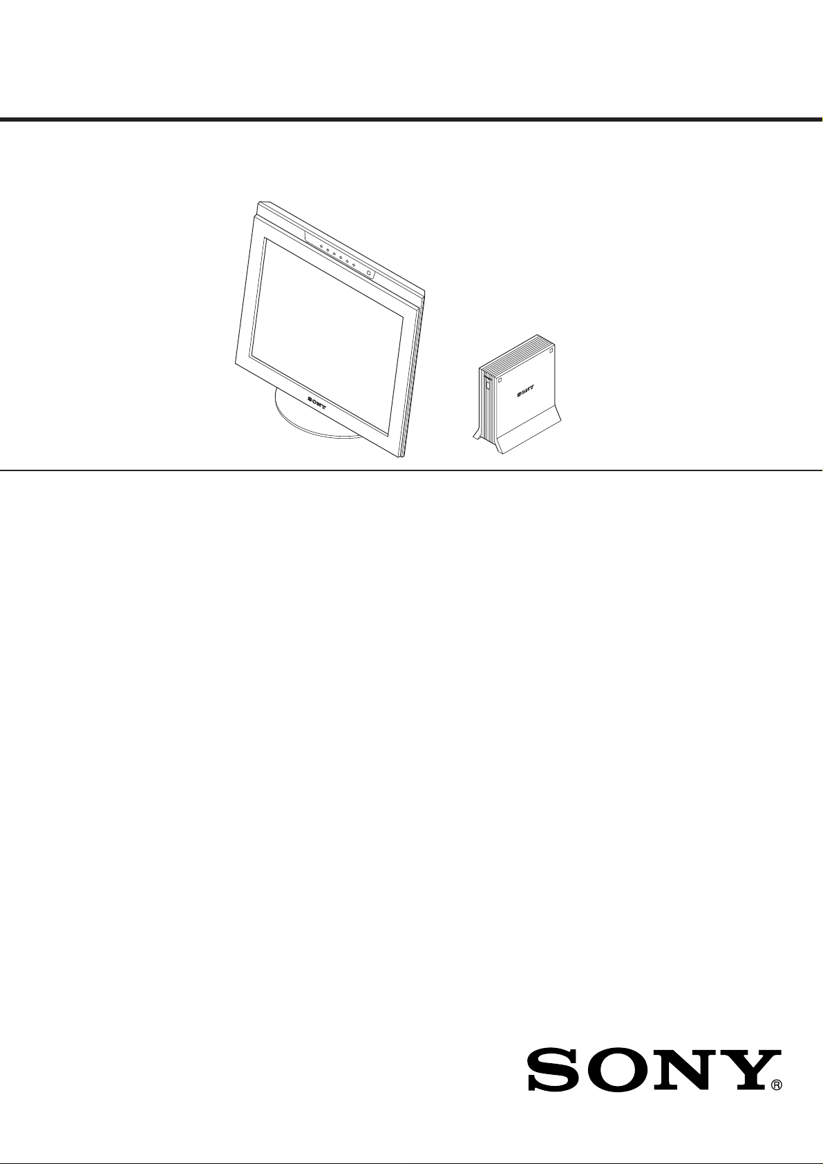
SDM-N80
p
SERVICE MANUAL
SPECIFICATIONS
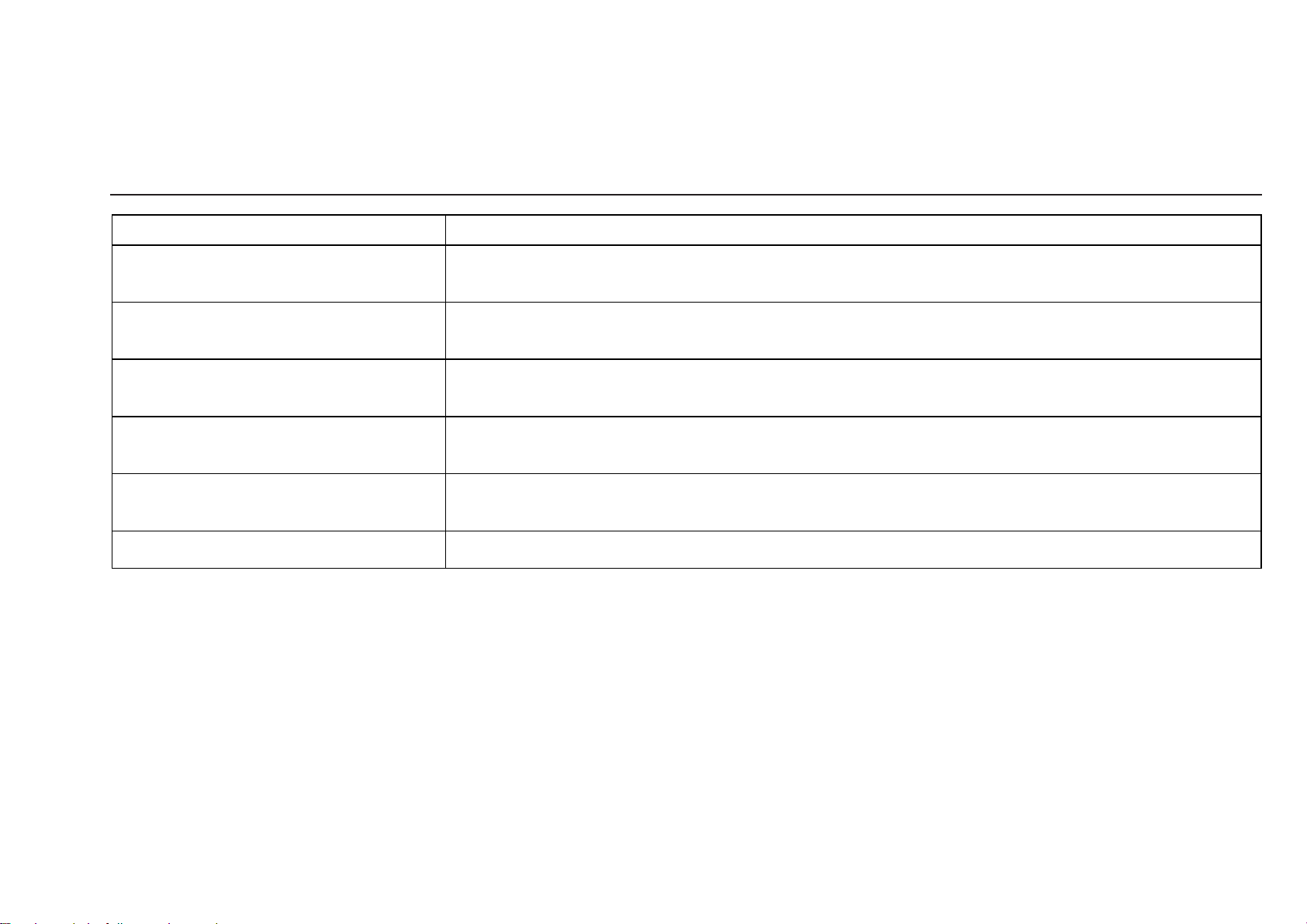
LCD panel Panel type: a-Si TFT Active Matrix
Picture size: 18.1 inch (46 cm)
Input signal format RGB operating frequency*
Horizontal: 28 – 107 kHz (analog
RGB signal)
28-92 kHz (digital RGB signal)
Vertical: 48 – 85 Hz**
Resolution** Horizontal: Max.1280 dots
Vertical: Max.1024 lines
Video input connector Analog RGB: HD15
Digital/analog RGB: DVI-I 29 pins
Input signal levels Analog RGB video signal
0.700 Vp-p, 75
SYNC signal
TTL level, 2 k
positive or negative
(Separate horizontal andvertical,
or composite sync)
0.3 Vp-p, 75
(Sync on green)
Digital RGB (DVI) video signal
TMDS (Single link)
Audio output 1 W × 2
Headphones jack Stereo minijack
Accepts impedance of 16 – 48
AUDIO IN jacks Stereo minijack × 2
Accepts impedance of 47 k
ts level 0.5 Vrms
Acce
Ω, positive
Ω,
Ω
,negative
Ω
Ω
Power requirements 100 – 240 V, 50 – 60 Hz, 0.7 – 0.4 A
Power consumption Max. 67 W
Operating temperature 5 – 35
Dimensions (w/h/d) Display (upright):
Mass Display:
Plug & Play DDC2B
* Recommended horizontal and vertical timing condition
Horizontalsyncwidth duty should be more than 4.8% oftotal
horizontal time or 0.8 µs, whichever is larger.
Horizontal blanking width should be more than 2.5 µsec.
Vertical blanking width should be more than 450 µsec.
**A 1600 × 1200 resolution signal is acceptable only when it is a
digital RGB signal and its vertical frequency is 60 Hz.
Design and specifications are subject to change without notice.
US Model
Canadian Model
AEP Model
Chassis No. SCC-L37A-A
SLM1
°
C
Approx. 432 400 195 mm
1
/
8
(17
Media engine:
Approx. 94 × 212 × 204 mm
3
/
4
× 8
(3
Approx. 6.5 kg (14 lb 5 oz)
Media engine:
Approx. 1.5 kg (3 lb 5 oz)
CHASSIS
3
3
/
4
× 8
/4inches)
× 7
1
/8inches)
× 15
3
/
8
TFT LCD COLOR COMPUTER DISPLAY

1.5 k
Ω
0.15 µF
AC
Voltmeter
(0.75 V)
To Exposed Metal
Parts on Set
Earth Ground
SAFETY CHECK-OUT
After correcting the original service problem, perform the following safety
checks before releasing the set to the customer:
1. Check the area of your repair for unsoldered or poorly-soldered
connections. Check the entire board surface for solder splashes and
bridges.
2. Check the interboard wiring to ensure that no wires are “pinched” or
contact high-wattage resistors.
3. Check that all control knobs, shields, covers, ground straps, and
mounting hardware have been replaced. Be absolutely certain that you
have replaced all the insulators.
4. Look for unauthorized replacement parts, particularly transistors, that
were installed during a previous repair. Point them out to the customer
and recommend their replacement.
5. Look for parts which, though functioning, show obvious signs of
deterioration. Point them out to the customer and recommend their
replacement.
6. Check the line cords for cracks and abrasion. Recommend the
replacement of any such line cord to the customer.
7. Check the B+ and HV to see if they are specified values. Make sure your
instruments are accurate; be suspicious of your HV meter if sets always
have low HV.
8. Check the antenna terminals, metal trim, “metallized” knobs, screws, and
all other exposed metal parts for AC Leakage. Check leakage as
described below.
LEAKAGE TEST
The AC leakage from any exposed metal part to earth ground and from all
exposed metal parts to any exposed metal part having a return to chassis,
must not exceed 0.5 mA (500 microamperes).
Leakage current can be measured by any one of three methods.
1. A commercial leakage tester, such as the Simpson 229 or RCA WT540A. Follow the manufacturers’ instructions to use these instruments.
2. A battery-operated AC milliammeter. The Data Precision 245 digital
multimeter is suitable for this job.
3. Measuring the voltage drop across a resistor by means of a VOM or
battery-operated AC voltmeter. The “limit” indication is 0.75 V, so
analog meters must have an accurate low-voltage scale. The Simpson 250
and Sanwa SH-63Trd are examples of a passive VOMs that are suitable.
Nearly all battery operated digital multimeters that have a 2 V AC range
are suitable. (See Fig. A)
Fig. A. Using an AC voltmeter to check AC leakage.
SDM-N80 (E) 2

WARNING!!
NEVER TURN ON THE POWER IN A CONDITION IN WHICH THE
DEGAUSS COIL HAS BEEN REMOVED.
SAFETY-RELATED COMPONENT WARNING!!
COMPONENTS IDENTIFIED BY SHADING AND MARK ¡ ON THE
SCHEMATIC DIAGRAMS, EXPLODED VIEWS AND IN THE
PARTS LIST ARE CRITICAL FOR SAFE OPERATION. REPLACE
THESE COMPONENTS WITH SONY PARTS WHOSE PART
NUMBERS APPEAR AS SHOWN IN THIS MANUAL OR IN
SUPPLEMENTS PUBLISHED BY SONY. CIRCUIT ADJUSTMENTS THAT ARE CRITICAL FOR SAFE OPERATION ARE
IDENTIFIED IN THIS MANUAL. FOLLOW THESE PROCEDURES
WHENEVER CRITICAL COMPONENTS ARE REPLACED OR IMPROPER OPERATION IS SUSPECTED.
AVERTISSEMENT!!
NE JAMAIS METTRE SOUS TENSION QUAND LA BOBINE DE
DEMAGNETISATION EST ENLEVÉE.
ATTENTION AUX COMPOSANTS RELATIFS À LA SÉCURITÉ!!
LES COMPOSANTS IDENTIFIÉS PAR UNE TRAME ET UNE
MARQUE ¡ SONT CRITIQUES POUR LA SÉCURITÉ. NE LES
REMPLACER QUE PAR UNE PIÈCE PORTANT LE NUMÉRO
SPECIFIÉ. LES RÉGLAGES DE CIRCUIT DONT L’IMPORTANCE EST
CRITIQUE POUR LA SÉCURITÉ DU FONCTIONNEMENT SONT
IDENTIFIÉS DANS LE PRÉSENT MANUEL. SUIVRE CES
PROCÉDURES LORS DE CHAQUE REMPLACEMENT DE
COMPOSANTS CRITIQUES, OU LORSQU’UN MAUVAIS
FONCTIONNEMENT EST SUSPECTÉ.
SDM-N80 (E) 3
POWER SAVING FUNCTION
This monitor meets the power-saving guidelines set by VESA,ENERGYSTAR, and NUTEK. If the monitor is connected to a computer
or video graphics board that is DPMS (Display Power Management Signaling) compliant, the monitor will automatically enter the power
saving mode. It automatically enters the low power consumption mode when the user sensor detects the absence of a user.
Power consumption state Power consumption AC power indicator (power) indicator
normal operation W green green
1 low power consumption mode W* green green and orange alternate
2 power saving mode W* orange orange
(power): off W red off
AC power: off 0 W off off
*Figures reflectpower consumption when the computer connected to the USB upstream connector on the monitor is turned off.
< 67
< 8.5
< 1.3
< 1
SDM-N80 (E) 4

1 Low power consumption mode (user sensor)
2 Power saving mode
When the user sensor in the monitor detects the absence of a user,
the monitor enters low power consumption mode after about 20
seconds.The icon of user sensor appears and flashes on the screen
before the monitor enters this mode. In low power consumption
mode, the monitor is in a power saving state and shuts off power
to all circuitry (except for that of the sensors) regardless of the
setting of the computer.
The monitor returns to normal operation mode when the presence
of a user is detected by the user sensor.
When the monitor enters the power saving mode (as set according
to the computer’s settings), the power saving mode takes
precedence over the low power consumption mode. In this case,
the monitor stays in the power saving mode regardless of the
presence or absence of a user.
To return the monitor to normal operation mode, reset the
computer’s power saving mode.
If the user sensor does not seem to function properly, refer to the
instructions on the next page.
DPMS defines the active off state according to the state of the
sync signals supplied from the computer. This monitor’s power
consumption is input at approximately 1.3 W or less in this state
if the power saving function is set to ON.
When your computer enters the power saving mode, the input
signal is cut and NO INPUT SIGNAL appears on the screen.
After a few seconds, the monitor enters power saving mode.
Power saving
Sync signal state
state
active off (deep sleep)* horizontal: off / vertical: off
* “Deep sleep” is a power saving mode defined by the Environmental
Protection Agency.
Notes
• The p ower saving function may not work normally depending on the
pattern of supplied sync signals. In such a case, set the power saving
function to OFF.
• When you connect a computer whose power is connected to the USB
upstream connector on the monitor, the monitor will not enter the
power saving mode.
SDM-N80 (E) 5
DIAGNOSIS
Failre
+B failure
Horizontal / Vertical Deflection
failure, Thermal protector
ABL protector
HV failure
Aging / Self Test
Out of scan range
Aging mode: In the NO INPUT SIGNAL state with the POWER SAVE MODE in OFF state, press the MENU continuously for 10
seconds.
Amber → Off
(0.5 sec) (0.5 sec)
Amber → Off
(1.5 sec) (0.5 sec)
Amber → Off
(0.5 sec) (1.5 sec)
Amber → Off → Amber → Off
(0.25 sec) (0.25 sec) (0.25 sec) (1.25 sec)
Amber → Off → Green → Off
(0.5 sec) (0.5 sec) (0.5 sec) (0.5 sec)
Green (OSD indication)
Power LED
SDM-N80 (E) 6
TIMING SPECIFICATION
MODE AT PRODUCTION
RESOLUTION
CLOCK
– HORIZONTAL –
H-FREQ
H. TOTAL
H. BLK
H. FP
H. SYNC
H. BP
H. ACTIV
– VERTICAL –
V. FREQ (Hz)
V. T OTA L
V. BLK
V. F P
V. SYNC
V. B P
V. ACTIV
– SYNC –
INT (G)
EXT (H/V) /POLARITY
EXT (CS) /POLARITY
NIT/NON INT
MODE 0 MODE 1 MODE 2 MODE 3 MODE 4 MODE 5 MODE 6 MODE 7 MODE 8
640 X 480 640 X 480 640 X 480 640 X 480 720 X 400 720 X 400 720 X 480 800 X 600
25.175 MHz 30.240 MHz 31.500 MHz 36.000 MHz 28.350 MHz 35.500 MHz 31.505 MHz 36.000 MHz
31.469 kHz 35.000 kHz 37.500 kHz 43.269 kHz 31.500 kHz 37.927 kHz #DIV/01 35.162 kHz 35.156 kHz
usec usec usec usec usec usec usec usec usec
31.778 28.571 26.667 23.111 31.746 26.366 #DIV/01 28.44 28.444
6.356 7.407 6.349 5.333 6.349 6.085 #DIV/01 5.586 6.222
0.636 2.116 0.508 1.556 0.635 1.014 #DIV/01 1.079 0.667
3.813 2.116 2.032 1.556 3.81 2.028 #DIV/01 1.27 2
1.907 3.175 3.81 2.222 1.905 3.042 #DIV/01 3.282 3.556
25.422 21.164 20.317 17.778 25.397 20.282 #DIV/01 22.854 22.222
59.940 Hz 66.667 Hz 75.000 Hz 85.008 Hz 70.156 Hz 85.039 Hz #DIV/01 59.901 Hz 56.250 Hz
lines lines lines lines lines lines lines lines lines
525 525 500 509 449 446 #DIV/01 587 625
45 45 20 29 49 46 #DIV/01 107 25
10 3 1 1 12 1 #DIV/01 12 1
233333#DIV/01 2 2
33 39 16 25 34 42 #DIV/01 93 22
480 480 480 480 400 400 #DIV/01 480 600
NO NO NO NO NO NO NO NO NO
YES N/N YES N/N YES N/N YES N/N YES N/P YES N/P YES YES N/N YES N/N
NO NO NO NO NO NO NO NO NO
NON INT NON INT NON INT NON INT NON INT NON INT NON INT NON INT NON INT
SDM-N80 (E) 7

MODE AT PRODUCTION
RESOLUTION
CLOCK
– HORIZONTAL –
H-FREQ
H. TOTAL
H. BLK
H. FP
H. SYNC
H. BP
H. ACTIV
– VERTICAL –
V. FREQ (Hz)
V. T OTA L
V. BLK
V. F P
V. SYNC
V. B P
V. ACTIV
– SYNC –
INT (G)
EXT (H/V) /POLARITY
EXT (CS) /POLARITY
NIT/NON INT
MODE 9 MODE 10 MODE 11 MODE 12 MODE 13 MODE 14 MODE 15 MODE 16 MODE 17
800 X 600 800 X 600 800 X 600 800 X 600 848 X 480 832 X 624 1024 X 768 1024 X 768 1024 X 768
40.000 MHz 49.500 MHz 56.250 MHz 57.299 MHz 49.847 MHz 57.285 MHz 65.000 MHz 75.000 MHz 78.750 MHz
37.879 kHz 46.875 kHz 53.674 kHz 54.675 kHz 45.900 kHz 49.727 kHz 48.363 kHz 56.476 kHz 60.023 kHz
usec usec usec usec usec usec usec usec usec
26.4 21.333 18.631 18.29 21.787 20.11 20.677 17.707 16.66
6.4 5.172 4.409 4.328 4.815 5.586 4.923 4.053 3.657
1 0.323 0.569 0.558 1.083 0.559 0.369 0.32 0.203
3.2 1.616 1.138 1.117 1.204 1.117 2.092 1.813 1.219
2.2 3.232 2.702 2.653 2.488 3.91 2.462 1.92 2.235
20 16.162 14.222 13.962 17.012 14.524 15.754 13.653 13.003
60.317 Hz 75.000 Hz 85.061 Hz 86.648 Hz 88.269 Hz 74.553 Hz 60.004 Hz 70.069 Hz 75.029 Hz
lines lines lines lines lines lines lines lines lines
628 625 631 631 520 667 806 806 800
28 25 31 31 40 43 38 38 32
111193331
433363663
23 21 27 27 25 37 29 29 28
600 600 600 600 480 624 768 768 768
NO NO NO NO NO NO NO NO NO
YES P/P NO P/P YES P/P YES P/P YES P/P YES N/N YES N/N YES N/N YES P/P
NO NO NO NO NO NO NO NO NO
NON INT NON INT NON INT NON INT NON INT NON INT NON INT NON INT NON INT
SDM-N80 (E) 8

MODE AT PRODUCTION
RESOLUTION
CLOCK
– HORIZONTAL –
H-FREQ
H. TOTAL
H. BLK
H. FP
H. SYNC
H. BP
H. ACTIV
– VERTICAL –
V. FREQ (Hz)
V. T OTA L
V. BLK
V. F P
V. SYNC
V. B P
V. ACTIV
– SYNC –
INT (G)
EXT (H/V) /POLARITY
EXT (CS) /POLARITY
NIT/NON INT
MODE 18 MODE 19 MODE 20 MODE 21 MODE 22 MODE 23 MODE 24 MODE 25 MODE 26
1024 X 768 1152 X 864 1152 X 864 1152 X 870 1120 X 750 1152 X 900 1152 X 900 1170 X 584 1024 X 800
94.500 MHz 108.000 MHz 121.500 MHz 100.000 MHz 78.430 MHz 92.940 MHz 105.590 MHz 46.200 MHz 92.940 MHz
68.677 kHz 67.500 kHz 77.487 kHz 68.681 kHz 50.019 kHz 61.795 kHz 71.732 kHz 31.216 kHz 70.838 kHz
usec usec usec usec usec usec usec usec usec
14.561 14.815 12.905 14.56 19.992 16.182 13.941 32.035 14.117
3.725 4.148 3.424 3.04 5.712 3.787 3.031 6.71 3.099
0.508 0.593 0.527 0.32 2.193 0.323 0.152 0.801 0.258
1.016 1.185 1.053 1.28 1.428 1.377 0.909 2.792 1.033
2.201 2.37 1.844 1.44 2.091 2.087 1.97 3.117 1.808
10.836 10.667 9.481 11.52 14.28 12.395 10.91 25.325 11.018
84.997 Hz 75.000 Hz 86.057 Hz 75.062 Hz 60.047 Hz 65.950 Hz 76.068 Hz 50.026 Hz 84.031 Hz
lines lines lines lines lines lines lines lines lines
808 900 911 915 833 937 943 624 843
40 36 47 45 83 37 43 40 43
1113272232
3333104838
36 32 43 39 46 31 33 34 33
768 864 864 870 750 900 900 584 800
NO NO NO NO NO NO NO NO NO
YES P/P YES P/P NO P/P YES N/N YES N/N YES N/N YES N/N YES N/N YES N/N
NO NO NO NO NO NO NO NO NO
NON INT NON INT NON INT NON INT NON INT NON INT NON INT NON INT NON INT
SDM-N80 (E) 9
MODE AT PRODUCTION
RESOLUTION
CLOCK
– HORIZONTAL –
H-FREQ
H. TOTAL
H. BLK
H. FP
H. SYNC
H. BP
H. ACTIV
– VERTICAL –
V. FREQ (Hz)
V. T OTA L
V. BLK
V. F P
V. SYNC
V. B P
V. ACTIV
– SYNC –
INT (G)
EXT (H/V) /POLARITY
EXT (CS) /POLARITY
NIT/NON INT
MODE 27 MODE 28 MODE 29 MODE 30 MODE 31 MODE 32 MODE 33 MODE 34 MODE 35
1280 X 960 1280 X 960 1280 X 1024 1280 X 1024 1280 X 1024 1280 X 1024 1024 X 768
108.000 MHz 148.500 MHz 108.000 MHz 135.000 MHz 157.500 MHz 148.000 MHz 80.000 MHz
60.000 kHz 85.938 kHz 63.981 kHz 79.976 kHz 91.146 kHz 81.319 kHz 60.241 kHz - -
usec usec usec usec usec usec usec usec usec
16.667 11.636 15.63 12.504 10.971 12.297 16.6 - -
4.815 3.017 3.778 3.022 2.844 3.649 3.8 - -
0.889 0.431 0.444 0.119 0.406 0.27 0.4 - -
1.037 1.077 1.037 1.067 1.016 1.378 1.2 - -
2.889 1.508 2.296 1.837 1.422 2 2.2 - -
11.852 8.62 11.852 9.481 8.127 8.649 12.8 - -
60.000 Hz 85.002 Hz 60.020 Hz 75.025 Hz 85.024 Hz 77.006 Hz 74.927 Hz - -
lines lines lines lines lines lines lines lines lines
1000 1011 1066 1066 1072 1056 804 - -
40 51 42 42 48 32 36 - -
1111133- -
3333333- -
36 47 38 38 44 26 30 - -
960 960 1024 1024 1024 1024 768 - -
NO NO NO NO NO YES NO - -
YES P/P YES P/P YES P/P YES P/P YES P/P NO YES N/N - -
NO NO NO NO NO NO NO - -
NON INT NON INT NON INT NON INT NON INT NON INT NON INT - -
SDM-N80 (E) 10

MODE AT PRODUCTION
RESOLUTION
CLOCK
– HORIZONTAL –
H-FREQ
H. TOTAL
H. BLK
H. FP
H. SYNC
H. BP
H. ACTIV
– VERTICAL –
V. FREQ (Hz)
V. T OTA L
V. BLK
V. F P
V. SYNC
V. B P
V. ACTIV
– SYNC –
INT (G)
EXT (H/V) /POLARITY
EXT (CS) /POLARITY
NIT/NON INT
MODE 36 MODE 37 MODE 38 MODE 39 MODE 40 MODE 41 MODE 42 MODE 43 MODE 44
1280 X 1024 800 X 600 1024 X 768 1280 X 1024 1600 X 1200 1600 X 1200 1600 X 1200 1600 X 1200 1600 X 1200
135.000 MHz 50.000 MHz 71.640 MHz 100.000 MHz 162.000 MHz 175.500 MHz 189.000 MHz 202.500 MHz 229.500 MHz
81.130 kHz 48.077 kHz 53.946 kHz 60.680 kHz 75.000 kHz 81.250 kHz 87.500 kHz 93.750 kHz 106.250 kHz
usec usec usec usec usec usec usec usec usec
12.326 20.8 18.537 16.48 13.333 12.308 11.429 10.667 9.412
2.844 4.8 4.243 3.68 3.457 3.191 2.963 2.765 2.44
0.237 1.12 0.223 0.24 0.395 0.365 0.339 0.316 0.279
0.474 2.4 2.457 1.12 1.185 1.094 1.016 0.948 0.837
2.133 1.28 1.563 2.32 1.877 1.732 1.608 1.501 1.325
9.481 16 14.294 12.8 9.877 9.117 8.466 7.901 6.972
76.107 Hz 72.188 Hz 66.110 Hz 57.030 Hz 60.000 Hz 65.000 Hz 70.000 Hz 75.000 Hz 85.000 Hz
lines lines lines lines lines lines lines lines lines
1066 666 816 1064 1250 1250 1250 1250 1250
42 66 48 40 50 50 50 50 50
2378311111
864333333
32 23 36 34 46 46 46 46 46
1024 600 768 1024 1200 1200 1200 1200 1200
NO NO NO NO NO NO NO NO NO
YES N/N YES N/N YES N/N YES N/N YES P/P YES P/P YES P/P YES P/P YES P/P
NO NO NO NO NO NO NO NO NO
NON INT NON INT NON INT NON INT NON INT NON INT NON INT NON INT NON INT
SDM-N80 (E) 11

TABLE OF CONTENTS
Section Title Page Section Title Page
1. DISASSEMBLY
1-1. Rear Section Removal .......................................... 1-1
1-2. B Board Removal ................................................. 1-2
1-3. LCD Module Removal ......................................... 1-3
1-4. U Board, H Board Removal ................................. 1-4
1-5. US Board Removal .............................................. 1-5
1-6. Case (L)/(R) Assembly Removal.......................... 1-6
1-7. A Board Removal ................................................. 1-7
1-8. H2 Board Removal .............................................. 1-8
1-9. Q Board, Switching Regulator Removal .............. 1-9
2. ADJUSTMENTS ...................................................... 2-1
3. DIAGRAMS
3-1. Block Diagrams .................................................... 3-1
(1) Schematic Diagrams of
A (a, b, c, d, e, f) Board ....................... 3-9
(2) Schematic Diagrams of
B (a, b, c, d, e, f) Board ....................... 3-16
(3) Schematic Diagrams of H (a, b, c) Board .... 3-23
(4) Schematic Diagram of H2 Board ......................... 3-27
(5) Schematic Diagram of Q Board ........................... 3-29
(6) Schematic Diagram of U Board ............................ 3-31
(7) Schematic Diagram of US Board.......................... 3-33
3-5. Semiconductors .................................................... 3-35
4. EXPLODED VIEWS .............................................. 4-1
4-1. LCD Display ........................................................ 4-2
4-2. Media Engine ....................................................... 4-3
4-3. Packing Materials ................................................. 4-4
3-2. Frame Schematic Diagram.................................... 3-5
3-3. Circuit Boards Location........................................ 3-6
3-4. Schematic Diagrams and Printed Wiring
Boards ................................................................... 3-7
5. ELECTRICAL PARTS LIST ............................... 5-1
SDM-N80 (E) 12
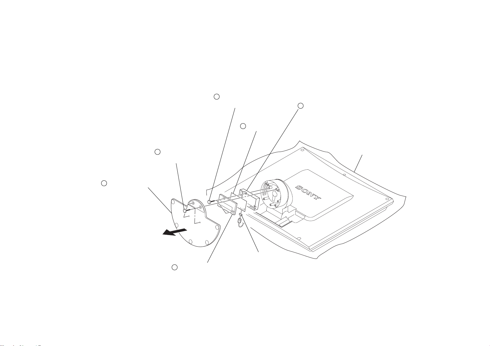
1-1. REAR SECTION REMOVAL
5
Two screws
(+BVTP 4X10)
SECTION 1
DISASSEMBLY
2
Remove the P hinge
cover (upper) in the
direction of arrow.
CN1203
1
Screw (M3)
3
Washer (M3)
6
Rear section
4
Screw
(+BVTP 3X14)
5
Two screw
(+BVTP 4X10)
Cushion
SDM-N80 (E) 1-1

1-2. B BOARD REMOVAL
2
3
Two screws
(+PSW 3X10)
CN1503
Heat sink
1
Two screws
(M3X4)
4
Three screws
(M3X4)
CN1302
CN1501
CN1451
CN1502
CN1301
CN1204
CN1300
CN1303
5
B board
Cushion
SDM-N80 (E) 1-2
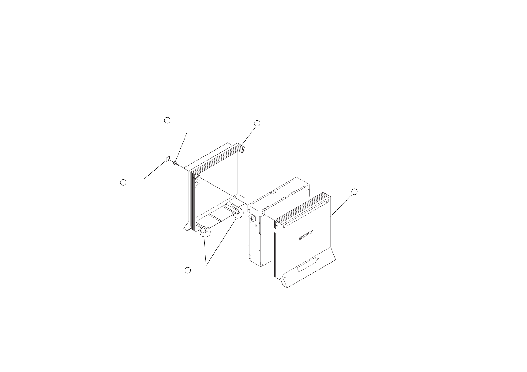
1-3. LCD MODULE REMOVAL
1
Two screws
(+BVTP 4X14)
2
Two harnesses
5
LCD MODULE (TFT)
3
Two screws
(+BVTP 4X14)
Cushion
4
Harness
SDM-N80 (E) 1-3
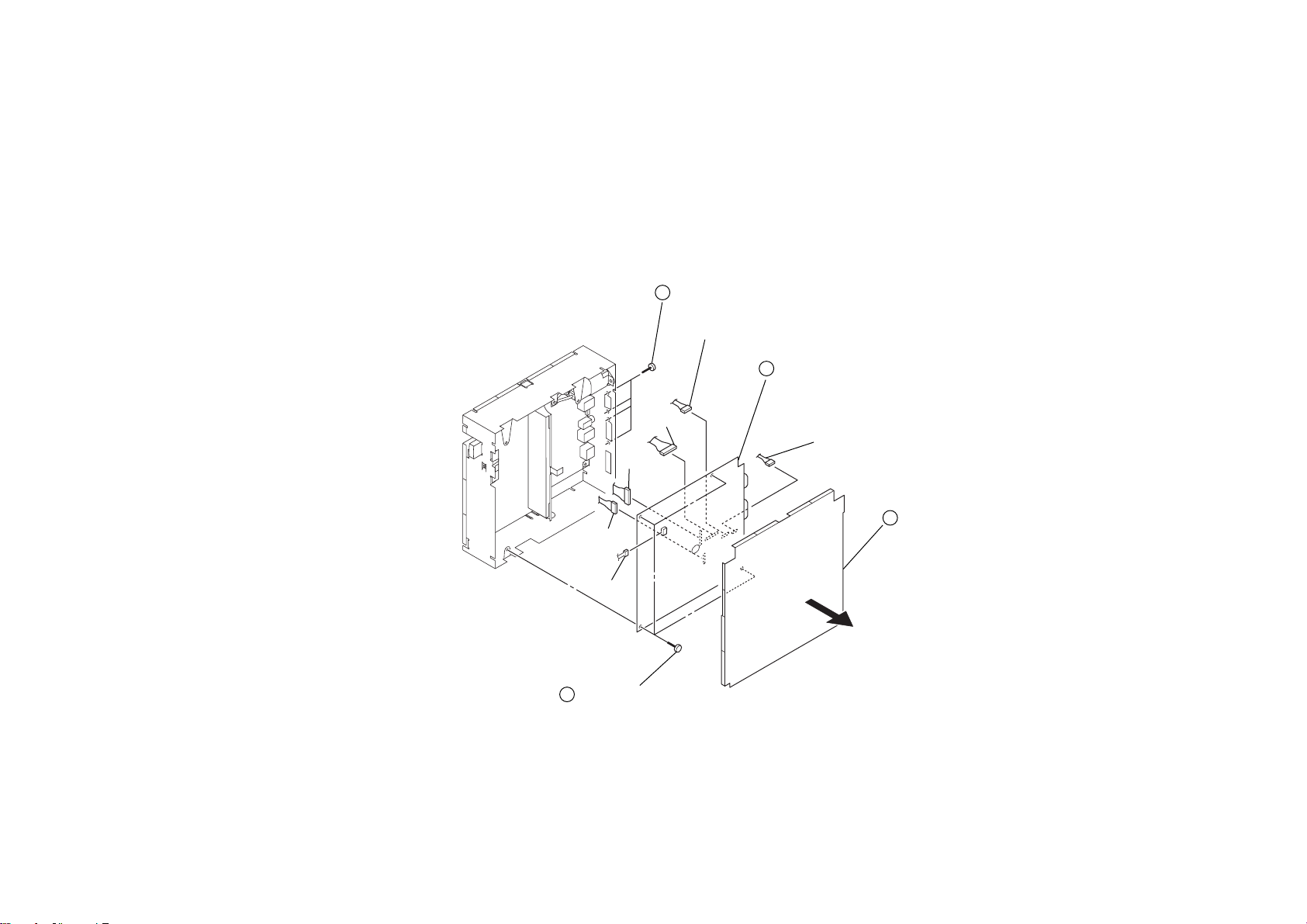
1-4. U BOARD, H BOARD REMOVAL
3
Two screws
(+BVTP 3X10)
5
H board
CN001
4
Harness
1
Screw (washer head)
(+P 3X12)
CN1701
2
U board
Cushion
SDM-N80 (E) 1-4
1-5. US BOARD REMOVAL
3
Two screws
(+BVTP 3X10)
6
US board
5
Shield case (USB)
2
Stand (bottom) cover
assembly
1
Four screws
(+BVTP 4X10)
4
Shield lid (USB)
Cushion
CN1101
SDM-N80 (E) 1-5
1-6. CASE (L)/(R) ASSEMBLY REMOVAL
2
Two screws
(+BVTP 3X14)
1
Sheet
4
Case (L) assembly
5
Case (R) assembly
3
Two claws
SDM-N80 (E) 1-6
1-7. A BOARD REMOVAL
CN501
CN302
CN502
3
Four hexagon screws
CN601
CN604
4
A board
CN602
1
Shield (R)
2
Four screws
(+BTP 3X6)
SDM-N80 (E) 1-7

1-8. H2 BOARD REMOVAL
3
Dowel
CN95
2
Screw (+BTP 3X6)
2
Shield (R)
4
H2 board
SDM-N80 (E) 1-8
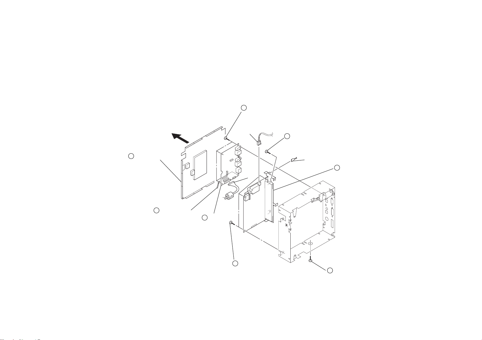
1-9. Q BOARD, SWITCHING REGULATOR REMOVAL
2
Four screws
(+BTP 3X6)
1
Shield (L)
3
Wire holder
4
Q board
CN1
CN960
7
Three screws
(+BTP 3X6)
6
Screw (+BTP 3X6)
GND
8
Switching regulator
5
Screw (+BTP 3X6)
SDM-N80 (E) 1-9

SECTION 2
Computer for jig
Audio input
to USB upstream
to INPUT 1
to INPUT 2
USB checker
Analog signal
generator
(VG-819, etc)
Digital signal
generator
(VG-828, etc)
USB mouse
[Measuring instrument position]
H/ L side:
C/ O side:
H Center
V Center
V Center
H Center
ADJUSTMENTS
Connect the personal computer, monitor, and signal generator as shown below, and control the monitor.
• Adjustment conditions
(1) impressed voltage:10%UP than rating voltage
(2) time: 30 minutes or more
(3) temperature: 25 ± 3˚C
(4) Brightness: Aging mode
• Adjustment of preset mode
Check the screen in the following five modes of the preset frequencies.
< Signal mode >
1. MODE 0 (640x480 60Hz)
2. MODE 11 (800x600 85Hz)
3. MODE 18 (1024x768 85Hz)
4. MODE 29 (1280x1024 60Hz)
5. MODE 40 (1600x1200 60Hz)
1.Generate the crosshatch signal.
2.Observing the ends, check that both ends can be seen or a white line at the end is not far away
from the edge of display area.
Note: Deviation up to 2 dots is allowable.
OK if either left or right side satisfies the above specification.
• Adjustment of white balance (Analog input 1)
SDM-N80 (E) 2-1

1.Adjustment of 9300K
(1) Receive MODE 29 (1280x1024 60Hz) 80IRE with the input 1. Set SOURCEID1=00h.
(2) Set R_USER_DRV=235.
Set R_USER_BKG=132.
(3) Make adjustment with G/B_USER_DRV to set the chromaticity within the specification.
x adjustment ..... Make adjustment with B_USER_DRV.
(The value y also changes.)
B_USER_DRV UP Values x and y decrease.
B_USER_DRV DOWN Values x and y increase.
y adjustment ..... Make adjustment with G_USER_DRV.
G_USER_DRV UP Value y increases.
G_USER_DRV DOWN Value y decreases.
Spec: 9300K (x, y) = (0.285, 0.298)
Within 3JND at 80IRE
9300K (x, y) = (0.277, 0.287)
Within 4JND at 20IRE
Note: Make adjustment up to ± 0.002.
(4) Make the signal 20IRE all white to check that it is within the specification.
(5) Input a gray scale to check the picture quality.
(5) (4) If out of specification, adjust the B/G_USER_BKG so as to satisfy the specification.
(6) Input a gray scale to check the picture quality.
2. Adjustment of 6500K
(1) Receive MODE 29 (1280x1024 60Hz) 80IRE with the input 1. Set SOURCEID1=01h.
(2) Set R_USER_DRV=235.
Set R_USER_BKG=132.
(3) Make adjustment with G/B_USER_DRV to set the chromaticity within the specification.
x adjustment ..... Make adjustment with B_USER_DRV.
(The value y also changes.)
B_USER_DRV UP Values x and y decrease.
B_USER_DRV DOWN Values x and y increase.
y adjustment ..... Make adjustment with G_USER_DRV.
G_USER_DRV UP Value y increases.
G_USER_DRV DOWN Value y decreases.
Spec: 6500K (x, y) = (0.314, 0.328)
Within 3JND at 80IRE
6500K (x, y) = (0.298, 0.317)
Within 4JND at 20IRE
Note: Make adjustment up to ± 0.002.
(4) Make the signal 20IRE all white to check that it is within the specification.
(5) Input a gray scale to check the picture quality.
(5) (4) If out of specification, adjust the G/B_USER_BKG so as to satisfy the specification.
(6) Input a gray scale to check the picture quality.
3. Adjustment of 5000K
(1) Receive MODE 29 (1280x1024 60Hz) 80IRE with the input 1. Set SOURCEID1=02h.
(2) Set R_USER_DRV=235.
Set R_USER_BKG=135.
(3) Make adjustment with G/B_USER_DRV to set the chromaticity within the specification.
x adjustment ..... Make adjustment with B_USER_DRV.
(The value y also changes.)
B_USER_DRV UP Values x and y decrease.
B_USER_DRV DOWN Values x and y increase.
y adjustment ..... Make adjustment with G_USER_DRV.
G_USER_DRV UP Value y increases.
G_USER_DRV DOWN Value y decreases.
Spec: 5000K (x, y) = (0.345, 0.358)
Within 3JND at 80IRE
5000K (x, y) = (0.316, 0.335)
Within 4JND at 20IRE
Note: Make adjustment up to ± 0.002.
(4) Make the signal 20IRE all white to check that it is within the specification.
(5) Input a gray scale to check the picture quality.
(5) (4) If out of specification, adjust the G/B_USER_BKG so as to satisfy the specification.
(6) Input a gray scale to check the picture quality.
4. Data copy to USER
Set SOURCEID1=03h and copy the data of R/G/B USER DRV and R/G/B USER BKG of
SOURCEID1=01h (Adjustment of 6500K).
5. Data copy to analog 2 input
(1) 9300K data copy
Set SOURCEID1=20h and copy the data of R/G/B USER DRV and R/G/B USER BKG of
SOURCEID1=00h (Adjustment of 9300K).
(2) 6500K data copy
Set SOURCEID1=21h and copy the data of R/G/B USER DRV and R/G/B USER BKG of
SOURCEID1=01h (Adjustment of 6500K).
(3) 5000K data copy
Set SOURCEID1=22h and copy the data of R/G/B USER DRV and R/G/B USER BKG of
SOURCEID1=02h (Adjustment of 5000K).
(4) USER data copy
Set SOURCEID1=23h and copy the data of R/G/B USER DRV and R/G/B USER BKG of
SOURCEID1=01h (Adjustment of 6500K).
SDM-N80 (E) 2-2

• Adjustment of white balance (Digital input)
1.Adjustment of 9300K
(1) Receive MODE 29 (1280x1024 60Hz) 80IRE with digital input. Set SOURCEID1=10h.
(2) Set R_USER_DRV=230.
Set R_USER_BKG=132.
(3) Make adjustment with G/B_USER_DRV to set the chromaticity within specification.
x adjustment ..... Make adjustment with B_USER_DRV.
(The value y also changes.)
B_USER_DRV UP Values x and y decrease.
B_USER_DRV DOWN Values x and y increase.
y adjustment ..... Make adjustment with G_USER_DRV.
G_USER_DRV UP Value y increases.
G_USER_DRV DOWN Value y decreases.
Spec: 9300K (x, y) = (0.285, 0.298)
Within 3JND at 80IRE
9300K (x, y) = (0.277, 0.287)
Within 4JND at 20IRE
Note: Make adjustment up to ± 0.002.
(4) Make the signal 20IRE all white to check that it is within the specification.
(5) Input a gray scale to check the picture quality.
(5) (4) If out of specification, adjust the R/B_USER_BKG so as to satisfy the specification.
(6) Input a gray scale to check the picture quality.
2.Adjustment of 6500K
(1) Receive MODE 29 (1280x1024 60Hz) 80IRE with digital input. Set SOURCEID1=11h.
(2) Set R_USER_DRV=220.
Set R_USER_BKG=128.
(3) Make adjustment with G/B_USER_DRV to set the chromaticity within the specification.
x adjustment ..... Make adjustment with B_USER_DRV.
(The value y also changes.)
B_USER_DRV UP Values x and y decrease.
B_USER_DRV DOWN Values x and y increase.
y adjustment ..... Make adjustment with G_USER_DRV.
G_USER_DRV UP Value y increases.
G_USER_DRV DOWN Value y decreases.
Spec: 6500K (x, y) = (0.314, 0.328)
Within 3JND at 80IRE
6500K (x, y) = (0.298, 0.317)
Within 4JND at 20IRE
Note: Make adjustment up to ± 0.002.
(4) Make the signal 20IRE all white to check that it is within the specification.
(5) Input a gray scale to check the picture quality.
(5) (4) If out of specification, adjust the G/B_USER_BKG so as to satisfy the specification.
(6) Input a gray scale to check the picture quality.
3. Adjustment of 5000K
(1) Receive MODE 29 (1280x1024 60Hz) 80IRE with the digital input. Set SOURCEID1=12h.
(2) Set R_USER_DRV=215.
Set R_USER_BKG=130.
(3) Make adjustment with R/B_USER_DRV to set the chromaticity within the specification.
x adjustment ..... Make adjustment with B_USER_DRV.
(The value y also changes.)
B_USER_DRV UP Values x and y decrease.
B_USER_DRV DOWN Values x and y increase.
y adjustment ..... Make adjustment with G_USER_DRV.
G_USER_DRV UP Value y increases.
G_USER_DRV DOWN Value y decreases.
Spec: 5000K (x, y) = (0.345, 0.358)
Within 3JND at 80IRE
5000K (x, y) = (0.316, 0.335)
Within 4JND at 20IRE
Note: Make adjustment up to ± 0.002.
(4) Make the signal 20IRE all white to check that it is within the specification.
(5) Input a gray scale to check the picture quality.
(5) (4) If out of specification, adjust the G/B_USER_BKG so as to satisfy the specification.
(6) Input a gray scale to check the picture quality.
4. Data copy to USER
Set SOURCEID1=13h and copy the data of R/G/B USER DRV and R/G/B USER BKG of
SOURCEID1=11h (Adjustment of 6500K).
SDM-N80 (E) 2-3

• User Sensor Adjustment
(4)After several seconds, check that IR_STATUS is 140 or less.
If IR_STATUS is not less than 140, write smaller value to
(1)After clearing up to the position of 2m in front of the set, place an object
for sensor detection in front of the set.
< Condition >
The panel must be vertical.
Object: A4 size paper for instance
Position: Flush with right end of the screen at the height of set stand
Distance: 1m from the screen
(TOP VIEW)
SET
1m
Object for detection
(SIDE VIEW)
SET
Object for detection
1m
IRLED_PW1.
(5) Raise IRLED_PW1 by 3 steps, and after about 2 seconds, check if
IR_STATUS is 160 or more.
If IR_STATUS is not more than 160, raise further the IRLED by 3
steps.
Repeat this until the IR_STATUS exceeds 160.
(6)When IR_STATUS exceeded 160, write value attained by adding 30 to
the IRLED_PW1 value to the following:
IRLED_PW1
IRLED_PW2
IRLED_PW3
(7)Write 0 to AUTO_PW for service saving.
(2)Set the AUTO_PW_SW to “1”.
(3)Write 40 to IRLED_PW1.
SDM-N80 (E) 2-4
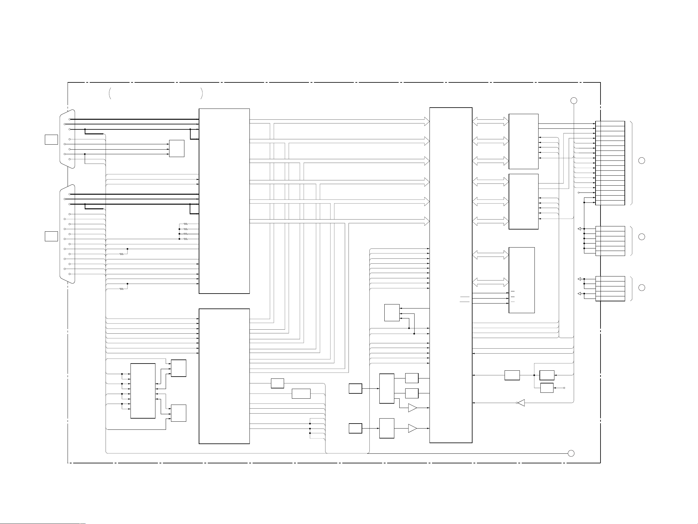
3-1. BLOCK DIAGRAMS
SECTION 3
DIAGRAMS
CN101
INPUT1
(HD15)
CN201
INPUT2
(DVI-I)
A (1/2)
GREEN1
DDCGND1
H1
V1
GREEN2
DDCGND2
SDA2
SCL2
H2
V2
RXC–
RXC+
RX0–
RX0+
RX1–
RX1+
RX2–
RX2+
A/D CONVERTER, TMDS RECEIVER, DDC,
SCAN CONVERETER, GVIF TRANSMITTER
139
133
124
IC203
ROM
IC202
ROM
132
141
136
126
135
100
101
103
105
106
108
143
111
112
113
6
9
10
98
99
90
89
87
86
84
83
81
80
ADPDN
SDA_SC
SCL_SC
GCLK
GFBK
GSOG
GHS_A
GCOAST
GHSFOUT
G_SEPIN
H1_ADIN
H2_ADIN
CLAMP
GBLKSPL
RXC–
RXC+
RX0–
RX0+
RX1–
RX1+
RX2–
RX2+
DDC_WP
SDA2
SCL2
ANALOG
DIGITAL
V2
10
12
13
2
3
9
5
6
OI1
OI2
OI3
OI4
C2
C3
C4
C1
SELECTOR
IC201
5
SDA
6
SCL
7
VCLK
IC101
ROM
7
VCLK
6
SCL
5
SDA
1
IO1
11
IO4
4
IO2
8
IO3
5
SDA
6
SCL
7
VCLK
A/D CONVERTER
R/CrN1
B/CbIN1
G/YIN1
SOGIN1
XPOWER SAVE
SDA
SCL
R/CrIN2
B/CbIN2
G/YIN2
SOGIN2
XCLK
CLK
1/2XCLK
1/2CLK
DSYNC/DIVOUT
SOGOUT
HOLD
EVEN/ODD
G/YOUT
SYNCIN1
SYNCIN2
CLPIN
TMDS RECEIVER
RXC–
RXC+
RX0–
RX0+
RX1–
RX1+
RX2–
RX2+
IC102
IC204
21, 22, 24 – 28, 31 208, 213 – 216, 221 – 223
GRE0 – 7 GRE0 – 7
RA0 – 7
34 – 41 190 – 192, 197 – 200, 207
GRO0 – 7 GRO0 – 7
RB0 – 7
45, 44, 51 – 53 26, 51, 52, 77, 78, 102, 109, 110
GBE0 – 7 GBE0 – 7
BA0 – 7
56 – 58, 60 – 64 23, 24, 48, 49, 74, 75, 99, 100
GBO0 – 7 GBO0 – 7
BB0 – 7
68 – 75 128, 133, 135, 181 – 184, 189
GGE0 – 7 GGE0 – 7
GA0 – 7
78, 81 – 85,
87, 88
GGO – 7 GGO0 – 7
GB0 – 7
30 – 37
QE16 – 23
GRE0 – 7
69 – 75, 77
QQ16 – 23
GRO0 – 7
10 – 17
QE0 – 7
GBE0 – 7
49 – 56
QQ0 – 7
GBO0 – 7
20 – 27
QE8 – 15
GGE0 – 7
59 – 66
QE8 – 15
GG0 – 7
PDO
SCDT
PD
ODCK
DE
VSYNC
HSYNC
9
8
2
44
46
SW
Q201
INVERTER
Q310
PDO
SCDT
PD
GCLK
GPEN
GVS_D
H348
GHS_D
GFBK
X401
21.6MHz
V347
X402
21.6MHz
GHS
GVS
GHSFOUT
GBLKSPL
GFBK
GCLK
GSOG
GPEN
GCOART
SDA_SC
SCL_SC
PRE_PXOFF
PRE_ADCPD
BL_MUTE
AU_MUTE
PX_WD
IC406
PLL CLOCK
MULTIPLIER
1
X1
IC407
PLL CLOCK
MULTIPLIER
1
X1 CLK
103, 104, 111, 112, 117 – 120
IC408
ROM
WP
SCL
SDA
S1
S0
CLK
IC401
SCAN CONVERTER
GRE0 –7
GRO0 – 7
GBE0 –7
GBO0 –7
GGE0 –7
GGO0 –7
144
GHS
159
GVS
166
GHSFOUT
141
GBLKSPL
136
GFBK
158
GCLK
151
GSOG
152
GPEN
142
GCOART
7
6
5
5
5
SW
Q406
SW
Q405
IC409
83
PORTA4
53
PORTA0
54
PORTA1
4
PORTB3
58
PORTB4
31
PORTB5
5
PORTB6
32
PORTB7
34
26
341
65
DCKEXT
315
32
MCKEXT
DRE0 – 7
DBE0 – 7
DGE0 – 7
DRO0 – 7
DBO0 – 7
DGO0 – 7
A1 – 18
D0 – 15
PORTA2
ROMOE
ROMWE
DENG
DCLK
DHS
DVS
RXD
TXD
RESET
PORTA5
231, 237 – 240,
248, 273, 274
DRE0 – 7
292, 295,
317 – 319, 322,
323, 349
DBE0 – 7
245, 270, 272,
297, 300, 324,
350, 351
DGE0 – 7
260, 286,
310 – 312,
337 – 339
DRO0 – 7
254, 279, 303,
305 – 307,
330, 332
DBO0 – 7
256, 257, 282,
283, 309, 333,
334, 336
DGO0 – 7
209 – 212, 217,
219, 220, 233,
235, 242 – 244,
249, 251, 275,
276, 301, 327
130, 131, 139,
140, 145, 146,
153 – 156, 163,
164, 169,
170 – 172
264
287
263
289
79
80
105
29
16 – 23
2 – 5,
44 – 47
6 – 11,
14, 15
16, 23
2 – 5,
44 – 47
6 – 11,
14, 15
3 – 11,
34 – 42
15 – 22,
24 – 31
GVIF TRANSMITTER
R0 – 7
B0 – 7
G0 – 7
R0 – 7
B0 – 7
G0 – 7
GVIF TRANSMITTER
IC410
FLASH ROM
A0 – 17A1 – 18
DQ0 – 15D0 – 15
227
WP
14186
QE
43185
WE
IC405
INVERTER
IC309 (1/3)
IC601
IC602
SDATAN
SDATAP
DE
SFTCLK
HSYNC
VSYNC
CE
SDATAN
SDATAP
DE
SFTCLK
HSYNC
VSYNC
CE
31
30
40
DCLK
41
42
43
26
GVIF_ON
31
30
40
DCLK
41
42
43
26
DENG
DCLK
INVERTER
Q404
IC404
RESET
DEN
DHS
DVS
DEN
DHS
DVS
DHS
DVS
GVIF_ON
DVS
RXD
TXD
RX_RSTN
RESET_SC
+3.3V
PANEL_MODE
1
CPU_ST
PANEL_MODE
SUB_SCL
SUB_SDA
AUDIO_R
AUDIO_L
USB POWER
D–
D+
HOTPLUG
+5V
+18V
+4V
+6V
CN603
SDATAN-B
4
SDATAP-B
6
SDATAN-A
9
SDATAP-A
11
B-CPU-ST
15
PANEL MODE
16
SCL
17
SDA
18
AUDIO-R
24
AUDIO-L
26
USB POWER
31
USB SIG–
33
USB SIG+
35
HOTPLUG
36
STBY6V
13
PANEL/DVIF 18V
2
BL18V
38
CN604
+18V
1
+18V
2
+18V
3
+18V
4
+18V
5
+18V
6
CN502
CONV_4V
1
CONV_4V
2
CONV_4C
3
CONV_6V
7
CONV_6V
8
A
TO B BOARD
CN1201
B
TO Q BOARD
CN961
C
TO Q BOARD
CN963
2
B-SS3558<U/C>-BD1-EPS05
SDM-N80 (E) 3-1

A (2/2)
IC302
CPU
1
µ-COM, SYNC_IRQ GENERATOR,
SYNC SEPARATOR, INPUT SELECT
H1 75
H2 76
V1
V2
GREEN1 97
GREEN2 98
GHS 65
GVS 23
CLAMP 82
G_SEPIN 83
GHS_A 84
GHS_D
GVS_D
H1
H2
H3
V1
V2
V3
H1_ADIN
H2_ADIN
DDC_GND1 113
DDC_GND2 114
ADPDN 101
SCDT 77
PDO 100
PD 99
DDC_WP 102
PRE_PXOFF 40
PRE_ADCPD 41
BL_MUTE 50
AU_MUTE 51
PX_WD 52
ANALOG 61
SYNC_IRQ
GENERATOR
IC103,
Q101 – Q128
SYNC
SEPARATOR
IC301, IC308
IC314, Q304
H_SEPIN
V_SEPIN
INPUT
SELECT
IC310 – IC313
INVERTER
Q305
SYNC_IRQ1
SYNC_IRQ2
COMP1
COMP2
HIN
VIN
POLH
EXIH
POLV
EXIV
65
IC309
(2/3)
IC304
EEP ROM
X302
32.768kHz
X301
4MHz
7
WC
6
SCL
5
SDA
85
58
74
73
92
93
103
55
56
57
SYNC1_IRQ
SYNC2_IRQ
COMP1
COMP2
HIN
VSIN
SYNC_SEP1
SYNC_SEP2
SYNC_SEP3
SYNC_SEP4
ANA_DIG
X0A
X1A
X0
X1
INPUT_SEL
EEP_WP
EEP_SCL
EEP_SDA
DDC_GND1
DDC_GND2
ADP_DN
SCDT
PDD
PD
DDC_WP
P73/DA0
P74/DA1
P84/AN4
P85/AN5
P86/AN6
DIGITAL
VSOUT
PANEL_DET2
PANEL_MODE
RESET_SC
GVIF_ON
SUB_SDA
SUB_SCL
SUB_IRQ
P_MEM
SC_SEL
SC_RX
SC_TX
ECS_RX
ECS_TX
WDT
HST
RESET
WDT_STOP
TCK
TAUX
MD2
MD0
USB_SEL
HUBON
USB1_EXIST
USB2_EXIST
AUDIO_SEL
LED_GREEN
LED_RED
POWER_ON
PON_4
PON_6
PON_13
PON_S33
24
HOTPLUG
53
PANEL_MODE
60
RESET_SC
116
GVIF_ON
81
SVB_SDA
70
SVB_SCL
71
72
112
14
12
13
9
10
118
86
90
117
11
95
87
89
69
66
64
67
68
110
109
111
106
107
108
105
DVS
CPU_ST
+6V
IC305 D-FF
3
1CK
11
2CK
5
1Q
SW
Q307
3
+5V
2
IO IO IO IO
IC501
+5V REG
1PR
2PR
IC303 RESET/WDT
3
8
IC509
+
1
–
+5V
1D
CLK
RSTN
2
4
10
RCT
SW
Q306
IC502
+3.3V REG
INVERTER
Q302
6
SW
Q501, 502
INVERTER
Q303
FLASH SW
Q301
+4V
+3.3V +4V +3.3V +4V
+5V
+2.5V
IC504
+3.3 REG
IC503, IC505
+3.3V REG
4
Y
IC306
TXD
45
IC307
6
2
A
1
OE
+3.3V +6V +5V +4V
RXD
IC309
(3/3)
3
1
2
IOIO
IC507, IC508
+5V REG
+2.5V REG
9
8
10 9
IC506
8
11
13
12
POWER_ON
M_RSTN
M_RSTN
PON_4
PON_6
PON_13
+2.5V
+6V
POWER_ON
PON_4
PON_6
PON_13
ANALOG
DIGITAL
D+
D–
USB POWER
AUDIO_R
AUDIO_L
+5V
+6V
STBY_6V
1
STBY_6V
2
POWERON
5
PON_4
6
PON_6
7
PON_13
8
ANALOG
12
DIGITAL
13
RXD
10
TXD
11
PX_RSTN
10
RXD
7
TXD
8
TVPP1
3
TRES
4
TCK
6
TAUS
5
TAUX3
2
TMODE
1
D+
7
D–
6
US_P_CONT
5
HUBON
4
USB_SEL
3
UP2_EXIST
2
UP1_EXIST
1
AUDIO_R
1
AUDIO_L
3
AUDIO_SEL
5
LED_GREEN
2
LED_RED
3
STBY 5V
1
CONV_4V
1
CONV_4V
2
CONV_4V
3
CONV_6V
7
CONV_6V
8
CN501
CN301
CN602
CN601
CN302
CN502
D
TO Q BOARD
CN962
FLASH
E
TO Q BOARD
CN903
F
TO Q BOARD
CN932
G
TO Q BOARD
CN963
CN95
LED_GREEN
LED_RED
STBY 5V
+5V
G
R
LED DRIVE
Q96
3
2
+5V
4
LED DRIVE
Q95
H2 (AC POWER LED)
D95
AC
POWER
2
B-SS3558<U/C>-BD2-EPS05
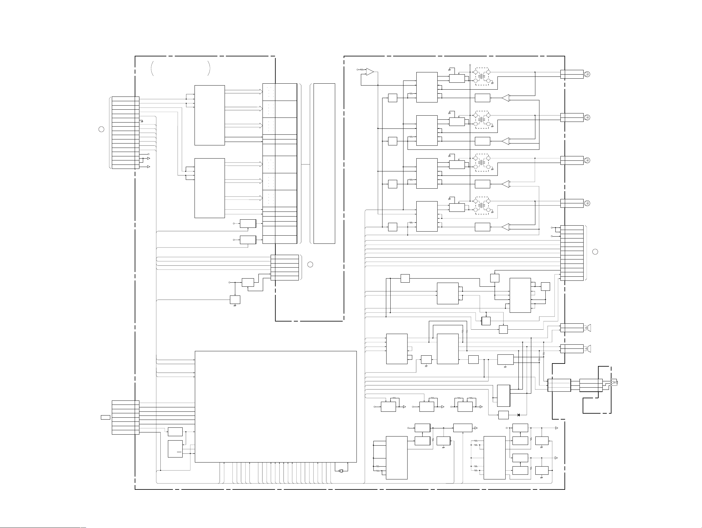
SDM-N80 (E) 3-2
A
TO A BOARD
CN603
FLASH
CN1201
SDATAN-A
SDATAP-A
SDATAN-B
SDATAP-B
B-CPU-ST
PANEL MODE
SCL
SDA
AUDIO_R
AUDIO_L
USB_POWER
USB SIG–
USB SIG+
HOT PLUG
PANEL /DVIF 18V
BL18V
STBY6V
CN1402
TMODE
TAUX3
TAUX
TCX
RXD
TXD
TVPP1
TRES
B
9
11
4
6
15
16
17
18
24
26
USB POWER
31
33
35
36
2
38
13
1
2
5
6
7
8
3
4
SUB µ-COM, GVIF RECEIVER,
D/D CONVERTER, INVERTER,
AUDIO, SENSOR AMP
B_CPU_ST
SCL
SDA
AUDIO_R
AUDIO_L
USB D–
USB D+
+5V
+18V
+6V
BL_ON_P
PON_P12
PROTECT
USB POWER
USB D–
USB D+
USB DET
B_CPU_ST
BL_ON_P
SDA
SCL
FLASH SW
Q1401
6
RCT
3
CK
8
RST
IC1401
RESET/ WDT
RESET
IC1201 GVIF RECEIVER
42
REFRQN
41
SDATAN
40
SDATAP
39
REFRQP
IC1202 GVIF RECEIVER
42
REFRQN
41
SDATAN
40
SDATAP
39
REFRQP
48
P71/IRQ1
92
P07/IRQ1
28
P50/SDA0/SOT0
29
P51/SCL0/SIN0
49
MD0
51
MD2
85
P00/AD00
18
P40/SCK
20
P42/SIN
19
P41/SOT
76
FLASH SW
52
HSTX
78
PA2
77
RSTX
SFTCLK
SFTCLK
99PON_P12
DE
DE
P16/AD14
18, 19, 22 – 25, 30, 31
R OLD0 – 7R0 –7
6, 7, 10 – 15
G OLD0 – 7G0 –7
2 – 5, 58, 59, 62, 63
B OLD0 – 7B0 –7
51
50
18, 19, 22 – 25, 30, 31
R NEW0 – 7R0 –7
6, 7, 10 – 15
G NEW0 – 7G0 –7
2 – 5, 58, 59, 62, 63
B NEW0 – 7B0 –7
51
50
+5V
+12V
+18V
SW
Q1204
P21/A17
P20/A16
P80/TIN0
2H_PWLEDR
1H_PWLEDG
59USB DET
BL ON SW
Q1205
+12V SW
Q1202, 1203
+18V SW
Q1201
P23/A19
P22/A18
4H_IRLED2
3H_IRLED1
P24/A20
5HP_STAT
P27/A23
9H_LEDCLK
8MUTE
A7 A8
A10 A11
A13 A14
A17 A18
A20 A21
A23 A24
A27 A28
A30 A31
A37 A38
A40 A41
A43 A44
A46 A47
B7 B8
B10 B11
B13 B14
B17 B18
B20 B21
B23 B24
B27 B28
B30 B31
B37 B38
B40 B41
B43 B44
B46 B47
A1 – A3
B1 – B3
P30/ALE
10H_LEDDATA
CN1204
RA0
RA7
GA0
GA7
BA0
BA7
A33 CLKA
A35 DEA
RB0
RB7
GB0
GB7
BB0
BB7
B33 CLKB
B35 DEB
A5
BLON_P
VCC
CN1203
PROTECT
2
USB POWER CONT
3
USB D–
4
USB D+
5
USB 18V
1
USB DET
8
IC1402 SUB-CPU
P63/AN3
P61/AN1
P60/AN0
P31/RDX
44H_BRTDET
41IROUT
39BL_STAT
38BL ON
ı
ı
ı
ı
ı
ı
P67/AN7
P65/AN5
46H_KEY
P86/IN2
P70/IRQ0
65H_REM
47H_PWKEY
H
TO US BOARD
CN1101
P96/PPG4
P94/PPG2
P92/PPG0
73H_PPG4
71H_PPG2
69PWM
DISPLAY
P11/AD09
P10/AD08
94AUSDA
93PROTECT
LCD
P12/AD10
95AUSCL
P13/AD11
P17/AD15
96PON_5AU
100PON_G33R
X0
82X183
X1401
4MHz
IC1300
+5V
3
+
1
2
–
SW
Q1308
SW
Q1306
SW
Q1304
BL ON
PWM
BL_STAT
H_PWKEY
H_KEY
H_PWLEDG
H_PWLEDR
H_LEDCLK
H_LEDDATA
H_BRTDET
H_PPG2
H_PPG4
IROUT
H_IRLED1
H_IRLED2
AUDIO_R
AUDIO_L
SDA
SCL
RESET
HP_STAT
MUTE
AUDIO_ON
PON_5AU
PON_G33R
AUDIO ON
SW
Q1301
AMP
Q1452
IC1502
AUDIO CONTROL
6
R_OUT
IN_R
11
L_IN
L_OUT
19
BOUT_R
SDA
20
SCL
BIN_R
BOUT_L
BIN_L
IO
16
11
13
12
+9V+18V
IC1503
+9V REG
310
NON1 OUT2
6
DT1
NON2
VREF
DT2
INV2
FB2
IC1310
INVERTER CONTROLLER
12
ENA
14
CT
5
ADJ
1
REF
INVERTER CONTROLLER
12
ENA
14
CT
5
ADJ
1
REF
INVERTER CONTROLLER
12
ENA
14
CT
5
ADJ
1
REF
INVERTER CONTROLLER
12
ENA
14
CT
5
ADJ
1
REF
16
17
15
14
13
12
IC1204, IC1205
+18V +5V
SWITCHING
Q1615
Q1610, 1611
14
1110G1
NDA
PDA
7
CMP
6
FB
3
LCLMP
2
HCLMP
IC1307
1110G1
NDA
PDA
7
CMP
6
FB
3
LCLMP
2
HCLMP
IC1305
1110G1
NDA
PDA
7
CMP
6
FB
3
LCLMP
2
HCLMP
IC1302
1110G1
NDA
PDA
7
CMP
6
FB
3
LCLMP
2
HCLMP
3
IN1+
5
IN2+
POWER AMP
6
IN_A–
15
IN_B–
1
RESET
SDOWN
Q1505
+3.3V REG
+3.3V+5V
PROTECT
Q1612
IO
AMP
G2
G2
G2
G2
IC1452 AMP
IC1501
S1 S2
SWITCHING
Q1312
S1 S2
SWITCHING
Q1311
S1 S2
SWITCHING
Q1310
S1 S2
SWITCHING
Q1309
IN1–
OUT1
OUT2
IN2–
3
OUT_A+
5
OUT_A–
18
OUT_B+
16
OUT_B–
20
HP_IN
IO
AUDIO +5V SW
Q1613, 1614
PROTECT
D1
D2
D1
D2
D1
D2
D1
D2
IC1203
+5V REG
AUDIO ON
+18V
HP SW
Q1506
T1303
4 8
2
CLAMP SW
Q1307
T1302
4 8
2
CLAMP SW
Q1305
T1301
4 8
2
CLAMP SW
Q1303
T1300
4 8
2
CLAMP SW
Q1300
Q1455
+5V+6V
IC1651 SW CONTROLLERIC1601 SW CONTROLLER
6
4
5
16
11
13
12
AMP
DT1
INV1
FB1
VREF
DT2
INV2
FB2
6
6
6
6
BUFF
Q1451
7
1
IC1309
(2/2)
7
IC1309
(1/2)
1
IC1304
(2/2)
7
IC1304
(1/2)
1
AMP
Q1456
MUTE SW
Q1503, 1504,
1508
IC1505 AMP
INB–
INA–
OUTB
OUTA
LATCH
Q1512
+18V
10
OUT2
14
NON2
OUT1
NON1
–
+
–
+
–
+
–
+
3
5
10
13
14
7
3
6
5
2
3
6
5
2
3
IC1451 AMP
IN1+
IN2+
IN3+
IN4+
OUT4
6
2
SWITCHING
Q1660, 1661
SWITCHING
Q1680, 1681
Q1665
AMP
Q1685
AMP
6
IN2–
7
OUT2
12
IN4+
8
OUT3
9
IN3–
1
OUT1
2
IN1–
PROTECT
Q1662
PROTECT
Q1682
PROTECT
B-SS3558<U/C>-BD3-EPS05
BUFF
Q1454
+5V
+12V
3
2
5
CN1503
R OUT
L OUT
HP_STAT
+12V
+5V
1
2
1
2
1
2
1
2
2
3
4
7
8
9
10
11
12
16
15
13
14
1
2
1
2
CN1303
HOT-4
COOL-4
CN1302
HOT-3
COOL-3
CN1301
HOT-2
COOL-2
CN1300
HOT-1
COOL-1
CN1451
5V (STBY)
5V (SENS)
12V
PWKEY
KEY
PWLED_G
PWLED_R
LEDCLK
LEDDATA
BRT DET
IRDET
IRLED1
IRLED2
CN1501
ROUT+
ROUT–
CN1502
LOUT+
LOUT–
LCD
BACK LIGHT
LCD
BACK LIGHT
LCD
BACK LIGHT
LCD
BACK LIGHT
I
TO H1 BOARD
CN001
(SPEAKER R)
(SPEAKER L)
CN1701
R OUT
L OUT
HP_STAT
U
(PHONE)
3
2
5
CN1700
(HEADPHONE)
SDM-N80 (E) 3-3
Q
D/D CONVERTER,
AUDIO IN,
USB CONTROL
CN902
3
2
1
CN901
3
2
1
CN930
INPUT1
AUDIO IN
CN931
INPUT2
AUDIO IN
AC IN
IC906
USB SELCTOR
1
10E
3
20E
5
2A
2
1A
9
3A
12
4A
AUDIO_L INPUT SELECT
1
V1
3
V2
AUDIO_R INPUT SELECT
1
V1
3
V2
SWITCHING
REGULATOR
11
DT2
13
INV2
12
FB2
REF
6
DT1
4
INV1
5
FB1
IC960 SW CONTROLLER
30E
40E
1B
4B
2B
3B
IC931
IC932
10
13
3
11
6
8
SW1
V_OUT
SW1
V_OUT
OUT2
NON2
OUT1
NON1
INVERTER
Q902
+3.3V
2
7
2
7
J961
ECS
POWER_ON
10
AMP
Q962, 963
14
7
AMP
Q966, 967
3
X901
12MHz
IO
IC902
RESET
8 7 6
5 4 3
2 1
CN960
+18V
8
+18V
7
+18V
6
STBY 6V
1
2
5
3
1
25
24
41
40
37
6
2
+18V
+6V
+18V
XOUT
XIN
DM0
DP0
RST
–IN2
–IN1
SWITCHING
Q964
SWITCHING
Q965
IC901
USB HUB
IC930
ISOLATOR
13
R1IN
14
T1OUT
2
V+
10
POW_1
43
DM1
42
DP1
7
OUT2
1
OUT1
IC965
RS232 DRIVER
R1OUT
T1IN
S960
ANALOG
DIGITAL
+5V
OI
IC963
+5V REG
POWER SW
Q901
+3.3V +5V
OI
IC903
+3.3V REG
+18V
IC961
+12V REG
+12V
OI
12
11
+6V
CONV_4V
1
CONV_4V
2
CONV_4V
3
CONV_6V
7
CONV_6V
8
USB_SEL
3
US_P_CONT
5
D–
6
D+
7
UP1_EXIST
1
UP2_EXIST
2
HUB ON
4
AUDIO_SEL
5
AUDIO_L
3
AUDIO_R
1
18V
1
18V
2
18V
3
18V
4
18V
5
18V
6
PON_12
8
STBY 6V
1
STBY 6V
2
RXD
10
TXD
11
ANALOG
12
DIGITAL
13
POWER_ON
5
CN963
CN903
CN932
CN961
CN962
G
TO A BOARD
CN502
E
TO A BOARD
CN602
F
TO A BOARD
CN601
B
TO A BOARD
CN604
D
TO A BOARD
CN501
I
TO B BOARD
CN1451
H
TO B BOARD
CN1203
CN001
LEDCLK
LEDDATA
PWKEY
PWLED_G
PWLED_R
KEY
BRTDET
IRDET
5V (STBY)
5V (SENS)
12V
IRLED2
IRLED1
CN1101
PROTECT
USB D–
USB D+
USB POWER CONT
USB 18V
10
14
12
11
13
19
18
17
9
5
6
7
8
+5V
2
4
5
3
1
+5V
+12V
IN1
AMP
Q016
IR SENSOR
Q015
LED DRIVE
Q013
LED DRIVE
Q011, 012
(USB CONTROL)
US
+5.5V
IC1103 SW CONTROLLER
14
12
16
6
4
5
3
CLOCK
2
+5V
+5V
KEY
+12V
D011 – D013
IR LED
7
3
DATA
+3.3V
SWITCHING
Q1106
BUFF
Q1101, 1102
PWKEY
LED_G
LED_R
IC011
AMP
3
7
OUT1
OUT2
IN2
35
OUT
VCC
IC011
LIGHT SENSOR
D013
D011, 012
PROTECT
Q1105
IC1105 +3.3V REG
IO IO
NON2
DT2
VREF
DT1
INV1
FBI
OUT1
NON1
+12V
Q0
4
D22
D21
TP001
MENU
D021, 022
MENU
IC1104
RESET
D35
D25
D025+D026
–
D035UPD036
DOWN
+5.5V
X1101
12MHz
Q2
Q6
Q3
6
TP002
TP003
–/
DOWN
IC031, 032, 041, 051, 052, 061, 071,
D027
VOLUME
41
DM0
40
DP0
37
RST
25
XOUT
24
XIN
Q1
5
7
10
D36 D23 D24 D28
D26 D37
TP004
+/
UP
BRIGHT
DET OUT
072, 081, Q001 – 006
D023
BRIGHT
IC1101
UBS HUB
DP1
DM1
DVR-1
POW_1
POW_2
DVR-2
DM2
DP2
Q4
8
D024
CONTRAST
42
43
31
10
11
32
3
2
TP005
CONTRAST
POWER SW
Q1104
POWER SW
Q1103
Q8
12
D028
INPUT
D37
OK
9
Q5
TP006
INPUT/
1
15
16
11
12
5
D38
CONTROL
Q10
14
+5V
A
V OUT1
V OUT2
Q9
13
D39D27
OK
D38
IN-1
D39
IN-2
IC1106 REGULATOR
FLG1
VC1
VC1
VC2
VC2
FLG2
IC36
LED
+5V
D001
G
S001
LED_R
LED_G
PWKEY
D001, S001
POWER
H
(USER CONTROL)
3
7
B-SS3558<U/C>-BD4-EPS05
CN1102
3
2
1
CN1103
1
2
3
SDM-N80 (E) 3-4

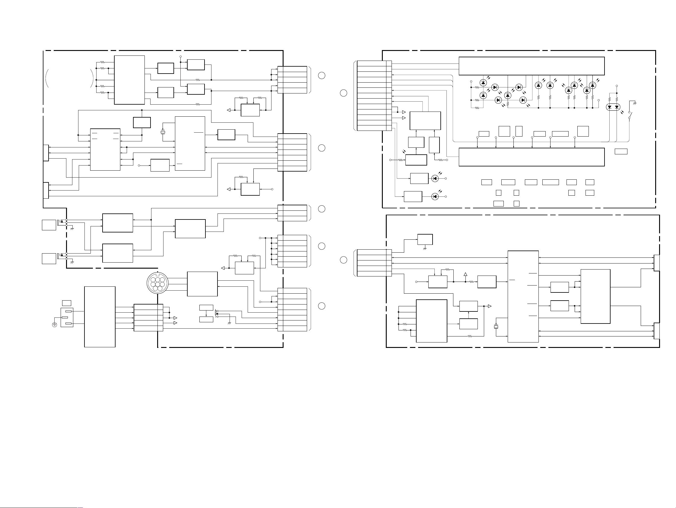
3-2. FRAME SCHEMATIC DIAGRAM
CN101
HD15P
INPUT1
CN201
DVI-I
INPUT1
FLASH
CN603
38P
PANEL/GVIF GND
1
PANEL/GVIF 18V
2
GVIF-GND
3
4
SDATAN-B
5
SDATAGND-A
6
SDATAP-B
7
GVIF-GND
8
GVIF-GND
9
SDATAN-A
10
SDATAGND-B
11
SDATAP-A
12
GVIF-GND
13
STBY5V
14
A/D CONVERTER, SYNC_IRQ GENERATOR,
A
TMDS RECEIVER, DDC, µ-COM, INPUT SELECT,
SYNC SEPARATOR, SCAN CONVERTER,
()
GVIF TRANSMITTER
CN301
10P
1
TMODE
2
TAUX3
3
TVPP1
4
TRES
5
TAUS
6
TCK
7
RXD
8
TXD
9
GND
10
PX_RSTN
A1
B1
A2
B2
A3
B3
A4
B4
A5
B5
A6
B6
A7
B7
A8
B8
A9
B9
A10
B10
A11
B11
A12
B12
A13
B13
A14
B14
A15
B15
A16
B16
A17
B17
A18
B18
A19
B19
A20
B20
A21
B21
A22
B22
A23
B23
A24
B24
A25
B25
A26
B26
A27
B27
A28
B28
A29
B29
A30
B30
A31
B31
A32
B32
A33
B33
A34
B34
A35
B35
CN401
70P
GND
A19
GND
A18
GND
A17
GND
A16
A15
A14
A13
A12
A11
A10
A9
A8
A7
A6
A5
A4
A3
A2
A1
A0
GND
BHENN
GND
ROMOEN
GND
ROMOEN
3.3V
ROMWEN
3.3V
ROMWEN
3.3V
CS2
3.3V
CS3
GND
RESETN
GND
NMI
GND
FCEN
GND
BOOTWE
GND
VPPEN
D15
D14
D13
D12
D11
D10
D9
D8
D7
D6
D5
D4
D3
D2
D1
D0
NC
NC
6V
6V
6V
6V
CN501
13P
STBY_6V
STBY_6V
GND
GND
POWERON
PON_4
PON_6
PON_13
GND
RXD
TXD
ANALOG
DIGITAL
CN502
10P
CONV_4V
CONV_4V
CONV_4V
GND
GND
GND
CONV_6V
CONV_6V
GND
GND
CN604
12P
+18V
+18V
+18V
+18V
+18V
+18V
GND
GND
GND
GND
GND
GND
CN601
AUDIO_R
AUDIO_GND
AUDIO_L
AUDIO_GND
AUDIO_SEL
CN602
UP1_EXIST
UP2_EXIST
USB_SEL
HUBON
US_P_CONT
CN302
4P
STBY5V
LED_GREEN
LED_RED
GND
1
2
3
4
5
6
7
8
9
10
11
12
13
1
2
3
4
5
6
7
8
9
10
1
2
3
4
5
6
7
8
9
10
11
12
5P
1
2
3
4
5
8P
1
2
3
4
5
6
D-
7
D+
8
GND
1
2
3
4
STBY 6V
2
STBY 6V
3
GND
4
GND
5
POWER_ON
6
PON_4
7
PON_6
8
PON_12
9
GND
10
RXD
11
TXD
12
ANALOG
13
DIGITAL
1
CONV_4V
2
CONV_4V
3
CONV_4V
4
GND
5
GND
6
GND
7
CONV_6V
8
CONV_6V
9
GND
10
GND
CN961
1
18V
2
18V
3
18V
4
18V
5
18V
6
18V
7
GND
8
GND
9
GND
10
GND
11
GND
12
GND
CN932
1
AUDIO_R
2
AUDIO_GND
3
AUDIO_L
4
AUDIO_GND
5
AUDIO_SEL
CN903
1
UP1_EXIST
2
UP2_EXIST
3
USB_SEL
4
HUB ON
5
US_P_CONT
6
D-
7
D+
8
GND
STBY 5V
4
LED_GREEN
3
LED_RED
2
1
GND
CN963
10P
12P
5P
8P
CN95
4P
CN962
13P
1
CN-SENS
15
B-CPU-ST
16
PANEL MODE
17
SCL
18
SDA
19
GND
20
AUDIO-GND1
21
AUDIO-GND1
22
AUDIO-GND1
23
AUDIO-GND1
24
AUDIO-R
25
AUDIO-GND2
26
AUDIO-L
IEEE1394 TPB*
27
IEEE1394 TPB*
28
IEEE1394 TPA*
29
IEEE1394 TPA*
30
31
USB POWER
USB POWER GND
32
33
USB SIG-
USB SHIELD GND
34
35
USB SIG+
36
HOT PLUG
37
BL GND
BL18V
38
Q
D/D CONVERTER,
AUDIO IN,
()
USB CONTROL
8 7 6
J961
5 4 3
ECS
2 1
CN930
3P
INPUT1
AUDIO IN
CN931
3P
INPUT2
AUDIO IN
CN960
8P
8
+18V
+18V
+18V
GND
GND
GND
POWER_ON
STBY 6V
7
6
5
4
3
2
1
SWITCHING
REGULATOR
AC IN
H2
(AC POWER LED)
FLASH
CN603
38P
PANEL/GVIF GND
1
PANEL/GVIF 18V
2
GVIF-GND
3
4
SDATAN-B
5
SDATAGND-A
6
SDATAP-B
7
GVIF-GND
8
GVIF-GND
9
SDATAN-A
10
SDATAGND-B
11
SDATAP-A
12
GVIF-GND
13
STBY5V
14
CN-SENS
15
B-CPU-ST
16
PANEL MODE
17
SCL
18
SDA
19
GND
20
AUDIO-GND1
21
AUDIO-GND1
22
AUDIO-GND1
23
AUDIO-GND1
24
AUDIO-R
25
AUDIO-GND2
26
AUDIO-L
IEEE1394 TPB*
27
IEEE1394 TPB*
28
IEEE1394 TPA*
29
IEEE1394 TPA*
30
31
USB POWER
USB POWER GND
32
33
USB SIG-
USB SHIELD GND
34
35
USB SIG+
36
HOT PLUG
37
BL GND
BL18V
38
CN1402
10P
TMODE
1
1
TAUX3
2
2
TVPP1
3
3
TRES
4
4
TAUX
5
5
TCK
6
6
RXD
7
7
TXD
8
8
GND
9
9
SUB5V
10
10
20P
CN1451
12V
5V(STBY)
5V(SENS)
PON_5KY
123456789
19
20
12V
CN001
(20P)
PON_5KY
5V(STBY)
5V(SENS)
GND
GND
PWLED_G
PWLED_R
LEDDATA
IRLED1
IRLED2
IRDET
LEDCLK
PWKEY
KEY
101112131415161718
101112131415161718
GND
GND
KEY
PWKEY
H
(USER CONTROL)
PWLED_G
PWLED_R
LEDCLK
LEDDATA
IRLED1
IRLED2
IRDET
H_AGND
BRTDET
H_AGND
BRTDET
H_AGND
H_AGND
CN1700
(HEAD PHONE)
SUB µ-COM, GVIF RECEIVER,
B
D/D CONVERTER,
(
INVERTER, AUDIO, SENSOR AMP
8P
H_REV1
H_REV2
20
19
123456789
H_REV1
H_REV2
CN1203
USB 18V
1234567
1234567
8P
USB 18V
CN1101
US
(USB CONTROL)
U
(PHONE)
USB POWER CONT
USB D-
USB D+
PROTECT
USB D-
USB D+
PROTECT
USB POWER CONT
CN1701
7P
S-GND
S-GND
L OUT
R OUT
HP_STAT
(SPEAKER R)
(SPEAKER L)
USB SHIELD GND
USB GND
USB GND
USB SHIELD GND
GND
GND
USB DET
8
8
USB DET
7
6
5
4
3
2
1
)
1
2
3
4
5
1
2
1
2
CN1503
5P
GND
L OUT
R OUT
GND
HP-STAT
CN1501
ROUT+
ROUT-
CN1502
2P WHITE
LOUT+
LOUT-
2P RED
CN1204
FX10A-100S
A1
VCC
B1
VCC
A2
VCC
B2
VCC
A3
VCC
B3
VCC
A4
GND
B4
GND
A5
BLON-P
B5
WHT
A6
GND
B6
GND
A7
RA7
B7
RB7
A8
RA6
B8
RB6
A9
GND
B9
GND
A10
RA5
B10
RB5
A11
RA4
B11
RB4
A12
GND
B12
GND
A13
RA3
B13
RB3
A14
RA2
B14
RB2
A15
GND
B15
GND
A16
GND
B16
GND
A17
RA1
B17
RB1
A18
RA0
B18
RB0
A19
GND
B19
GND
A20
GA7
B20
GB7
A21
GA6
B21
GB6
A22
GND
B22
GND
A23
GA5
B23
GB5
A24
GA4
B24
GB4
A25
GND
B25
GND
A26
GND
B26
GND
A27
GA3
B27
GB3
A28
GA2
B28
GB2
A29
GND
B29
GND
A30
GA1
B30
GB1
A31
GA0
B31
GB0
A32
GND
B32
GND
A33
CLKA
B33
CLKB
A34
GND
B34
GND
A35
DEA
B35
DEB
A36
GND
B36
GND
A37
BA7
B37
BB7
A38
BA6
B38
BB6
A39
GND
B39
GND
A40
BA5
B40
BB5
A41
BA4
B41
BB4
A42
GND
B42
GND
A43
BA3
B43
BB3
A44
BA2
B44
BB2
A45
GND
B45
GND
A46
BA1
B46
BB1
A47
BA0
B47
BB0
A48
GND
B48
GND
A49
GND
B49
GND
A50
GND
B50
GND
CN1300
2P
BHS
1
HOT-1
2
COOL-1
CN1301
2P
BHS
1
HOT-2
2
COOL-2
CN1302
2P
BHS
1
HOT-3
2
COOL-3
CN1303
2P
BHS
1
HOT-4
2
COOL-4
B-SSS3558<U/C>-KESSENZU-EPS05
LCD
BACK LIGHT
LCD
BACK LIGHT
LCD
BACK LIGHT
LCD
BACK LIGHT
LCD
DISPLAY
SDM-N80 (E) 3-5
 Loading...