

Page 1
Sony Corporation
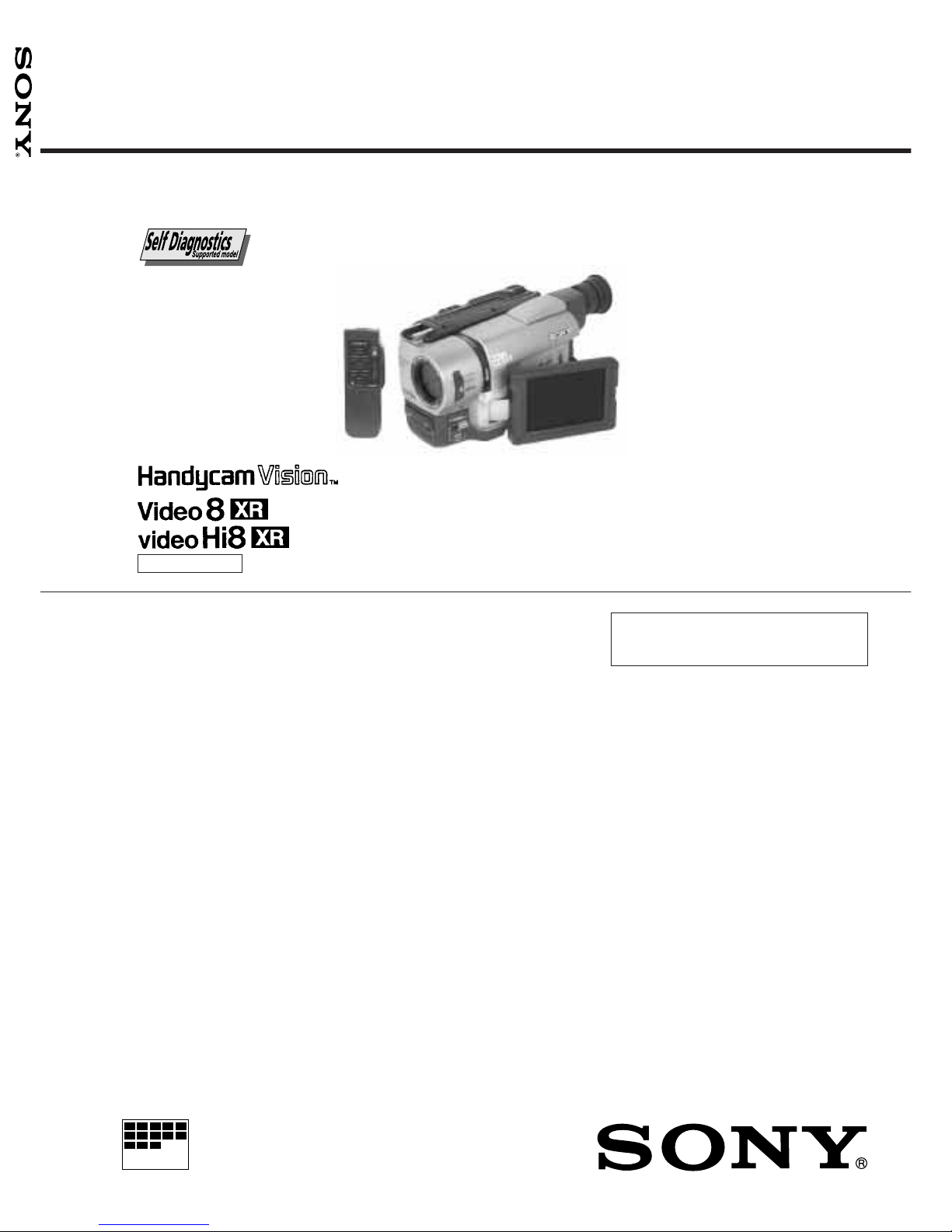
CCD-TRV3E/TRV13E/TRV23E/TRV45E/TRV55E/TRV65E/TRV69E/TRV75/TRV75PK/TRV715
SERVICE MANUAL
CCD-TRV3E/TRV13E/TRV23E/TRV45E/TRV55E/
TRV65E/TRV69E/TRV75/TRV75PK/TRV715
RMT-708/717
SERVICE MANUAL
MICROFILM
For MECHANISM ADJUSTMENTS, refer to
the “8mm Video MECHANICAL ADJUSTMENT
MANUAL VII” (9-973-801-11).
SPECIFICATIONS
US Model
Canadian Model
CCD-TRV75/TRV715
E Model
CCD-TRV3E/TRV23E/TR V45E/
TRV55E/TRV75/TRV75PK
AEP Model
CCD-TRV13E/TRV65E/TRV69E
UK Model
East European Model
North European Model
Russian Model
CCD-TRV13E/TRV65E
Hong Kong Model
CCD-TRV3E/TRV23E/TRV45E/TR V55E
Tourist Model
CCD-TRV3E/TRV55E/TRV75
Australian Model
CCD-TRV3E/TRV23E/TRV45E
Chinese Model
CCD-TRV3E/TRV23E/TR V45E/
TRV55E/TRV65E
HVIDEO CAMERA RECORDER
hVIDEO CAMERA RECORDER
— Continued on next page —
B MECHANISM
Photo : CCD-TRV55E
: RMT-708
CCD-TRV65E/TRV69E/TRV75/TRV75PK/TRV715
Video camera recorder
System
Video recording system
CCD-TRV75/TRV75PK/TRV715 : 4
rotary heads (SP/LP independent heads)
CCD-TRV3E/TRV13E/TRV23E/
TRV45E/TRV55E/TRV65E/TRV69E :
2 Rotary heads
Helical scanning FM system
Audio recording system
Rotary heads, FM system
Video signal
CCD-TRV75/TRV75PK/TRV715 :
NTSC color, EIA standards
CCD-TRV3E/TRV13E/TRV23E/
TRV45E/TRV55E/TRV65E/TRV69E :
PAL color CCIR standards
Usable cassette
8mm video format cassette
CCD-TRV3E/TRV13E/TRV23E/
TRV45E/TRV55E : standard 8
CCD-TRV65E/69E/TRV75/TRV75PK/
TRV715 : Hi8 or standard 8
Recording / Playback time
CCD-TRV75/TRV75PK/TRV715 :
(using 120 min. cassette)
SP mode: 2 hours
LP mode: 4 hours
CCD-TRV3E/TRV13E/TRV23E/
TRV45E/TRV55E/TRV65E/TRV69E :
(using 90 min. cassette)
SP mode: 1 hours and 30 minutes
LP mode: 3 hours
Fastforward/rewind time
CCD-TRV75/TRV75PK/TRV715 :
(using 120 min. cassette) Approx. 5 min.
CCD-TRV3E/TRV13E/TRV23E/
TRV45E/TRV55E/TRV65E/TRV69E :
(using 90 min. cassette) Approx. 5 min.
Image device
CCD (Charge Coupled Device)
Viewfinder
Electronic viewfinder
Monochrome
Lens
Combined power zoom lens
Filter diameter 17/16 in. (37 mm)
CCD-TRV13E (AEP,UK) :
16 x (Optical), 32 x (Digital)
CCD-TRV13E (EE,NE,RU) :
16 x (Optical), 160 x (Digital)
CCD-TRV65E (AEP,UK)/TRV75 (US,
CND)/TRV715 :
18 x (Optical), 72 x (Digital)
CCD-TRV23E/TRV45E/TRV55E/
TRV65E (EE,NE,RU,E,AUS,HK,CN)/
TRV75 (E, JE)/TRV75PK :
18 x (Optical), 220 x (Digital)
Focal distance
CCD-TRV3E/13E : 3/16 - 2 5/8 in.
(4.1 - 65.6 mm)
CCD-TRV23E/TRV45E/TRV55E/
TRV65E/TRV69E/TRV75/TRV75PK/
TRV715 : 3/16 - 8 in. (4.1 - 73.8 mm)
When converted to a 35 mm still camera
CCD-TRV3E/TRV13E :
1 9/16 - 24 7/8 in. (39.4 - 630 mm)
CCD-TRV23E :
1 9/16 - 28 in. (39.4 - 709 mm)
CCD-TRV45E/TRV55E/TRV65E/
TRV69E/TRV75/TRV75PK/TRV715 :
1 7/8 - 33 1/2 in. (47.2 - 850 mm)
Color temperature
Auto
Minimum illumination*
* Minimum illumination expresses the
light level a camcoder requires to
produce a picture.
CCD-TRV23E : 0.4 lux (F 1.4)
CCD-TRV3E/13E : 0.4 lux (F1.4)
(*Visible minimum low light 0.2 lux)
* Visible minimum low light expresses
the light level to produce a visible
signal.
CCD-TRV45E/TRV55E/TRV65E/
TRV69E/TRV75/TRV75PK/TRV715 :
0.7 lux (F 1.4)
CCD-TRV23E/TRV45E/TRV55E/
TRV65E/TRV69E/TRV75/TRV75PK/
TRV715 :
0 lux (in NightShot mode)*
* Object invisible for the dark can be
shot with infrared lighting.
Illumination range
CCD-TRV3E/TRV13E/TRV23E :
0.4 lux to 100,000 lux
CCD-TRV45E/TRV55E/TRV65E/
TRV69E/TRV75/TRV75PK/TRV715 :
0.7 lux to 100,000 lux
Recommended illumination
More than 100 lux
LCD screen
Picture
CCD-TRV3E/TRV13E/TRV23E/
TRV65E/TRV69E :
2.5 inches measured diagonally
2 x 1 1/2 in.(50.3 x 37.4 mm)
CCD-TRV45E/TRV55E :
3.5 inches measured diagonally
2 7/8 x 2 in.(72.4 x 50.4 mm)
CCD-TRV3E/TRV13E/TRV23E/TRV45E/TRV55E
Page 2

Mass (Approx.)
9.8 oz (280 g) excluding power cord
(Main lead)
Design and specifications are subject to
change without notice.
• Abbreviation
CND : Canadian Model
EE : East European Model
NE : North European Model
RU : Russian Model
CN : Chinese Model
HK : Hong Kong Model
AUS : Australian Model
JE : Tourist Model
Dimentions (Approx.)
CCD-TRV3E/TRV13E/TR V23E/
TRV65E/TRV69E :
4 1/4 x 4 1/4 x 8 1/4 in.
(107 x 107 x 209 mm)(w/h/d)
CCD-TRV45E/TRV55E/TRV75/
TRV75PK/TRV715 :
4 1/2 x 4 3/8 x 8 1/2 in.
(114 x 111 x 214 mm)(w/h/d)
Mass (Approx.)
CCD-TRV3E/TRV13E/TRV23E :
1 lb 15 oz (890 g)
CCD-TRV65E/TRV69E :
1 lb 15 oz (900 g)
CCD-TRV45E/TRV55E :
2 lb 1 oz (950 g)
CCD-TRV75/TRV75PK/TRV715 :
2 lb 1oz (940 g)
excluding the battery pack, lithium
battery, cassette and shoulder strap
2 lb 3 oz (1 kg)
including the battery pack NP-F330,
lithium battery CR2025, cassette and
shoulder strap
Microphone
CCD-TRV3E/TRV13E/TRV23E :
Monaural type
CCD-TRV45E/TRV55E/TRV65E/
TRV69E/TRV75/TRV75PK/TRV715 :
Stereo type
Supplied accessories
See page 4.
AC power adaptor
Power requirements
100 -240 V AC, 50/60 Hz
Power consumption
23 W
Output voltage
DC OUT: 8.4 V, 1.5 A in operating
mode
Operating temperature
32°F to 104°F(0°C to 40°C)
Storage temperature
-4°F to +140°F(-20°C to +60°C)
Dimentions (Approx.)
5 x 1 9/16 x 2 1/2 in. (125 x 39 x 62
mm)(w/h/d) excluding projecting parts
Earphone jack(CCD-TRV3E/
TRV13E/TRV23E only)
Monaural minijack (ø 3.5 mm)
LANC control jack
Stereo mini-minijack (ø 2.5 mm)
MIC jack
Mini jack, 0.388mV low impedance
with 2.5 to 3.0 V DC, output impedance
6.8 kilohms (ø 3.5 mm)
CCD-TRV3E/TRV13E/TRV23E :
Monaural type
CCD-TRV45E/TRV55E/TRV65E/
TRV69E/TRV75/TRV75PK/TRV715 :
Stereo type
Speaker
Dynamic speaker
Intelligent accessory shoe(CCD-
TRV45E/TRV55E/TRV65E/TRV69E/
TRV75/TRV75PK/TRV715 only)
8-pin connector
General
Power requirements
7.2 V (battery pack)
8.4 V (AC power adaptor)
Averege power
consumption(when using the
battery pack)
During camera recording using
LCD
CCD-TRV3E/TRV13E : 3.1 W
CCD-TRV23E : 3.2 W
CCD-TRV65E/TRV69E : 3.3 W
CCD-TRV45E/TRV55E : 3.5 W
CCD-TRV75/TRV75PK/TRV715 :
3.4 W
Viewfinder
CCD-TRV3E/TRV13E : 2.5 W
CCD-TRV23E/TRV75/TRV75PK/
TRV715 : 2.6 W
CCD-TRV45E/TRV55E/TRV65E/
TRV69E : 2.7 W
Operating temperature
32°F to 104°F(0°C to 40°C)
Storage temperature
-4°F to +140°F(-20°C to +60°C)
CCD-TRV75/TRV75PK/TRV715 :
3 inches measured diagonally
2 3/8 x 1 3/4 in.(59.5 x 43.2 mm)
On-screen display
TN LCD/TFT active matrix method
T otal dot number
CCD-TRV3E/TRV13E/TRV23E :
61,380 (279 x 220)
CCD-TRV65E/TRV69E :
84.260 (380 x 220)
CCD-TRV45E/TRV55E :
105,380 (479 x 220)
CCD-TRV75/TRV75PK/TRV715 :
89,622 (383 x 234)
Input and output connectors
S video input/output(CCD-TRV65E
(CN)/TRV75/TRV75PK/TRV715 only)
S video output(CCD-TRV65 (AEP,
UK, EE, NE, RU)/TRV69E only)
4-pin mini DIN
Luminance signal :
1 Vp-p, 75 ohms, unbalanced
CCD-TRV75/TRV75PK/TRV715 :
Chrominance signal :
0.286 Vp-p, 75 ohms, unbalanced
CCD-TRV65E (CN) :
Chrominance signal :
0.3 Vp-p, 75 ohms, unbalanced
Video input(CCD-TRV45E/TRV55E/
TRV65E (CN)/TRV75/TRV75PK/
TRV715 only)/output
Phono jack, 1 Vp-p, 75 ohms, unbalanced
Audio input (CCD-TRV45E/TRV55E/
TRV65E (CN)/TRV75/TRV75PK/
TRV715 only)/output
CCD-TRV13E/TRV13E/TRV23E :
Monaural, Phone jack, 327 mV
CCD-TRV45E/TRV55E/TRV69E/
TRV75/TRV75PK/TRV715 : Phono
jacks (2: stereo L and R) 327 mV, (at
output impedance 47 kilohms)
impedance less than 2.2 kilohms
RFU DC OUT
Special minijack, DC 5V
Headphone jack(CCD-TRV45E/
TRV55E/TRV65E/TRV69E/TRV75/
TRV75PK/TR V715 only)
Stereo minijack (ø 3.5 mm)
ATTENTION AU COMPOSANT AYANT RAPPORT
À LA SÉCURITÉ!!
LES COMPOSANTS IDENTIFIÉS P AR UNE MARQUE ! SUR LES
DIAGRAMMES SCHÉMATIQUES ET LA LISTE DES PIÈCES SONT
CRITIQUES POUR LA SÉCURITÉ DE FONCTIONNEMENT. NE
REMPLACER CES COMPOSANTS QUE P AR DES PIÈCES SONY
DONT LES NUMÉROS SONT DONNÉS DANS CE MANUEL OU
DANS LES SUPPLÉMENTS PUBLIÉS PAR SONY.
SAFETY-RELATED COMPONENT WARNING !!
COMPONENTS IDENTIFIED BY MARK ! OR DOTTED LINE WITH
MARK ! ON THE SCHEMATIC DIAGRAMS AND IN THE PARTS
LIST ARE CRITICAL TO SAFE OPERATION. REPLACE THESE
COMPONENTS WITH SONY PARTS WHOSE PART NUMBERS
APPEAR AS SHOWN IN THIS MANUAL OR IN SUPPLEMENTS
PUBLISHED BY SONY.
1. Check the area of your repair for unsoldered or poorly-soldered
connections. Check the entire board surface for solder splashes
and bridges.
2. Check the interboard wiring to ensure that no wires are “pinched”
or contact high-wattage resistors.
3. Look for unauthorized replacement parts, particularly transistors,
that were installed during a previous repair. Point them out to
the customer and recommend their replacement.
4. Look for parts which, though functioning, show obvious signs
of deterioration. Point them out to the customer and recommend
their replacement.
5. Check the B+ voltage to see it is at the values specified.
6. Flexible Circuit board Repairing
• Keep the temperature of the soldering iron around 270 °C during
repairing.
• Do not touch the soldering iron on the same conductor of the
circuit board (within 3 times).
• Be careful not to apply force on the conductor when soldering
or unsoldering.
SAFETY CHECK-OUT
After correcting the original service problem, perform the following
safety checks before releasing the set to the customer:
– 2 –
Page 3
– 3 –
CCD-
TRV715
US,CND
NTSC
RMT-708¬G
18X
72X
760H¬¬
5heads
Stereo¬¬¬GG3 inch¬¬GG¬¬
CCD-
TRV69E
AEP
PAL
RMT-717¬G
18X
72X
760H¬¬
3heads
Stereo¬GGGG2.5 inch¬¬G¬¬¬
CCD-
TRV65E
AEP,UK,EE,
NE,RU
PAL
RMT-708¬G
18X
72X(Note 2)
760H¬¬
3heads
Stereo¬GGGG2.5 inch¬¬GG¬¬
CCD-
TRV13E
AEP,UK,EE
NE,RU
PALGG¬16X
32X (Note 1)
510HGG
3heads
MonoGGGGG2.5 inchGGGGGG
CCD-
TRV3E
E,AUS,HK,
CN,JE
PALGG¬16X
100X
510HGG
3heads
MonoGGGGG2.5 inchGGGGGG
CCD-
TRV75
US,CND
NTSC
RMT-708¬G
18X
72X
760H¬¬
5heads
Stereo¬¬¬GG3 inch¬¬GG¬¬
CN
PAL
RMT-708¬G
18X
220X
760H¬¬
3heads
Stereo¬¬GGG2.5 inch¬¬GG¬¬
CCD-
TRV55E
E,HK,CN,JEPAL
RMT-708G¬
18X
220X
760H¬¬
3heads
Stereo¬¬G¬¬3.5 inch¬¬GG¬¬
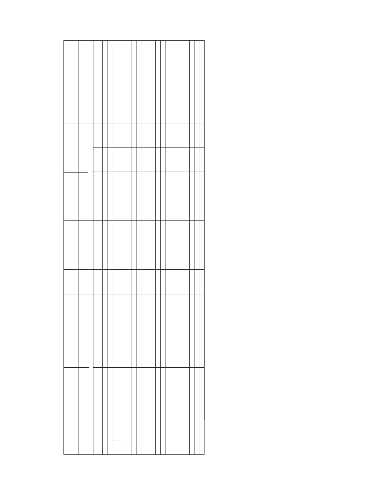
Table for difference of function
Model
Destination
Classification
Color System
Remote commander
Hi8
Standard 8
Lens Optical
Digital
CCD
Night shot
Steady shot
5heads/3heads
Audio System
TBC&DNR
VTR REC
Laser Link
Photo mode
Digital effect
LCD
Monitor IN
Intelligent Accessory Shoe
Normal Accessory Shoe
Time code
Display window indicator backlight
Manual Focus
CCD-
TRV23E
E,HK,AUS,
CN
PAL
RMT-708G¬
18X
220X
510H¬G
3heads
MonoGGGG¬2.5 inchGG¬GG¬
CCD-
TRV45E
E,HK,AUS,
CN
PAL
RMT-708G¬
18X
220X
760H¬¬
3heads
StereoG¬GGG3.5 inch¬¬GG¬¬
Remark
16X : LSV601A, 18X : LSV600A
¬ : LSV600A
¬ : with SE-66/67 board SE451,452,IC451
¬ : with VC-195 board IC204
¬ : with FK-8500 block S005,007
¬ : with VC-195 board IC751
¬ : VC-195 board IC204 is CXD3131
¬ : VC-195 board IC204 is CXD3131
2.5 inch : PD-92 board, 3/3.5 inch : PD-93 board
¬ : with VC-195 board X151
¬ : with VC-195 board CN909
¬ : with VC-195 board IC701
¬ : with CF-50/51 board Q003,005
¬ : with MF-8500/MR-8500
Note1 : EE,NE,RU model is 160X
Note2 : EE,NE,RU model is 220X
• Abbre viation
CND : Canadian Model
EE : East European Model
NE : North European Model
RU : Russian Model
HK : Hong Kong Model
AUS : Australian Model
JE : Tourist Model
CN : Chinese Model
TYPE A TYPE B TYPE C TYPE D TYPE E TYPE F
CCD-
TRV75/
TRV75PK
E,JE/E
NTSC
RMT-708¬G
18X
220X
760H¬¬
5heads
Stereo¬¬¬GG3 inch¬¬GG¬¬
Page 4
– 4 –
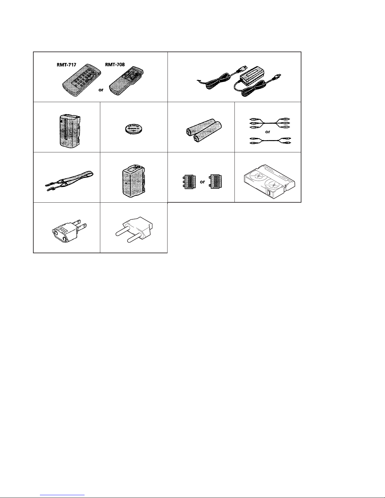
Supplied accessories
1 Wireless Remote Commander (1)
RMT-717 : CCD-TRV69E
RMT-708 : Except CCD-TRV69E
2 AC-L10A/L10B/L10C AC power adaptor
3 NP-F330 Battery pack (1)
4 CR2025 Lithium Battery (1)
The lithium battery is already installed in your camcorder.
5 Size AA (R6) battery for Remote Commander
(2)
6 A / V connecting cable (1)
Stereo : Except CCD-TRV3E/TRV13E/TRV23E
Monaural : CCD-TRV3E/TRV13E/TRV23E
7 Shoulder strap (1)
8 Battery case (1)
CCD-TRV75 : US, CND
1
4
8
7
3
2
56
90
• Abbreviation
CND : Canadian Model
EE : East European Model
NE : North European Model
RU : Russian Model
HK : Hong Kong Model
AUS : Australian Model
JE : Tourist Model
CN : Chinese Model
!¡
9 21 pin adaptor (1)
VMC-91 : CCD-TRV65E : AEP, EE, NE, RU, UK/TRV69E
VMC-89 : CCD-TRV13E
!º 8mm tape
CCD-TRV75 : US/TRV715 : US
!¡ 2 pin conversion adaptor (1)
CCD-TRV3E : E, HK/TRV23E : E, HK/TRV45E : E, HK/
TRV55E : E, HK/TRV75 : E/TRV75PK
!™ 2 pin conversion adaptor (1)
CCD-TRV3E : JE/TRV55E : JE/TRV75 : JE
!™
Page 5
– 5 –
Battery terminal
‘
DC IN terminal
Battery SIG terminal
Battery switch
Battery terminal
’
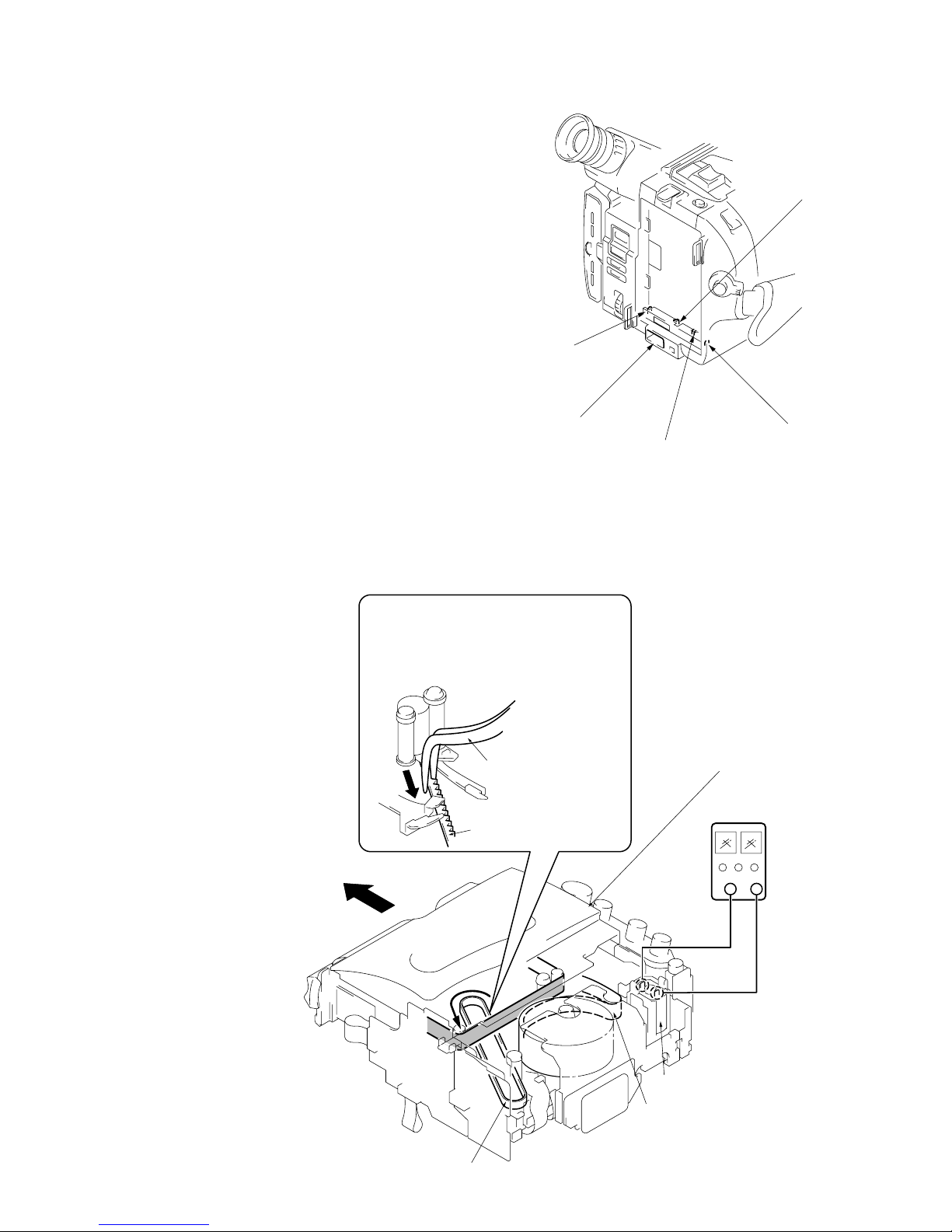
SERVICE NOTE
6
Pull the timing belt in the direction of arrow A
with a pinsette while pressing the cassette lid
(take care not to damage) to adjust the
bending of a tape.
7
Let go your hold the cassette
lid and rise the cassette
compartment to take out a cassette.
A
Pinsette
Timing belt
Press the cassette lid not to rise the
cassette compartment
+
–
[DC power supply]
(+5V)
Loading motor
Adjust the bending of a tape
Timing belt
1 Refer to 2-1-1. to remove the front panel assembly.
2 Refer to 2-1-2. to remove the cabinet (R) assembly.
3 Refer to 2-1-11. to remove the battery panel assembly.
4 Refer to 2-1-13. to remove the cabinet (L) assembly.
5 Add +5V from the DC POWER SUPPLY and unload with a
pressing the cassette lid.
2. TO T AKE OUT A CASSETTE WHEN NOT EJECT (FORCE EJECT)
1. POWER SUPPL Y DURING REPAIRS
In this unit, about 10 seconds after power is supplied (8.4V) to the
battery terminal using the service power cord (J-6082-223-A), the
power is shut off so that the unit cannot operate.
This following three methods are available to prevent this. Take
note of which to use during repairs.
Method 1.
Connect the servicing remote commander RM-95 (J-6082-053-B)
to the LANC jack, and set the remote commander switch to the
“ADJ” side .
Method 2.
Press the battery switch of the battery terminal using adhesive tape,
etc.
Method 3.
Use the DC IN terminal. (Use the AC power adaptor.)
Page 6
– 6 –
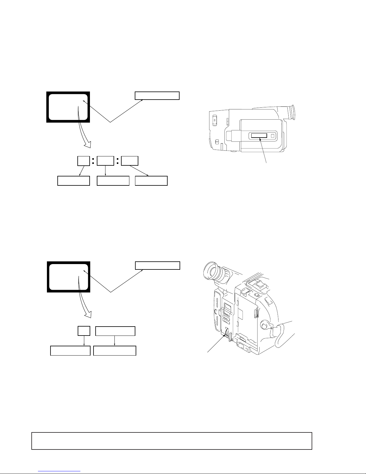
Note: The self-diagnosis display data will be backed up by the coin-type lithium battery. When this coin-type lithium battery is
disconnected, the self-diagnosis data will be lost by initialization.
1. Self-diagnosis Function
When problems occur while the unit is operating, the self-diagnosis
function starts working, and displays on the viewfinder or Display
window what to do. This function consists of two display; selfdiagnosis display and service mode display.
Details of the self-diagnosis functions are provided in the Instruction
manual.
SELF-DIAGNOSIS FUNCTION
2. Self-diagnosis display
When problems occur while the unit is operating, the counter of the
viewfinder or Display window shows a 4-digit display consisting
of an alphabet and numbers, which blinks at 3.2 Hz. This 5-character
display indicates the “repaired by:”, “block” in which the problem
occurred, and “detailed code” of the problem.
3. Service Mode Display
The service mode display shows up to six self-diagnosis codes shown in the past.
3-1. Display Method
While pressing the “STOP” key, set the switch from OFF to “VTR or PLAYER”, and continue pressing the “STOP” key for 5 seconds
continuously. The service mode will be displayed, and the counter will show the backup No. and the 5-character self-diagnosis codes.
3-2. Switching of Backup No.
By rotating the control dial, past self-diagnosis codes will be shown in order. The backup No. in the [] indicates the order in which the
problem occurred. (If the number of problems which occurred is less than 6, only the number of problems which occurred will be shown.)
[1] : Occurred first time [4] : Occurred fourth time
[2] : Occurred second time [5] : Occurred fifth time
[3] : Occurred third time [6] : Occurred the last time
3-3. End of Display
Turning OFF the power supply will end the service mode display.
Viewfinder
Display window
Blinks at 3.2 Hz
Refer to page7
Self-diagnosis Code table
C : Corrected by customer
H : Corrected by dealer
E : Corrected by service engineer
Repairede by :
Block
Detailed Code
Indicates the appropriate step to be taken
E. g.
31 ... Reload the tape.
32 ... Turn on power again.
C
3 1 1 1
C : 3 1 : 1 1
C : 3 1 : 1 1
Viewfinder
Display window
Lights up
Order of previous errors
Backup No.
Self-diagnosis codes
[3]
C : 3 1 : 1 1
3 C : 3 1 : 1 1
[3] C : 3 1 : 1 1
Display window
Control dial
Page 7
– 7 –
Remove the cassette, and insert it again after one hour.
Clean with the optional cleaning cassette.
Use the InfoLITHIUM battery.
Load the tape again, and perform operations from the beginning.
Load the tape again, and perform operations from the beginning.
Load the tape again, and perform operations from the beginning.
Load the tape again, and perform operations from the beginning.
Load the tape again, and perform operations from the beginning.
Load the tape again, and perform operations from the beginning.
Load the tape again, and perform operations from the beginning.
Load the tape again, and perform operations from the beginning.
Load the tape again, and perform operations from the beginning.
Load the tape again, and perform operations from the beginning.
Load the tape again, and perform operations from the beginning.
Load the tape again, and perform operations from the beginning.
Load the tape again, and perform operations from the beginning.
Remove the battery or power cable, connect, and perform operations
from the beginning.
Remove the battery or power cable, connect, and perform operations
from the beginning.
Remove the battery or power cable, connect, and perform operations
from the beginning.
Remove the battery or power cable, connect, and perform operations
from the beginning.
Remove the battery or power cable, connect, and perform operations
from the beginning.
Remove the battery or power cable, connect, and perform operations
from the beginning.
Remove the battery or power cable, connect, and perform operations
from the beginning.
Remove the battery or power cable, connect, and perform operations
from the beginning.
Remove the battery or power cable, connect, and perform operations
from the beginning.
Remove the battery or power cable, connect, and perform operations
from the beginning.
Remove the battery or power cable, connect, and perform operations
from the beginning.
Remove the battery or power cable, connect, and perform operations
from the beginning.
Remove the battery or power cable, connect, and perform operations
from the beginning.
Inspect the lens block focus reset sensor (Pin !ª of CN551 of VC-195
board) when focusing is performed when the focus dial is rotated in the
focus manual mode and the focus motor drive circuit (IC552 of VC-195
board) when the focusing is not performed.
Note : Use the remote commander RM-95 only for the model without
the focus dial.
Inspect the lens block zoom reset sensor (Pin @¡ of CN551 of VC-195
board) when zooming is performed when the zoom lens is operated and
the zoom motor drive circuit (IC552 of VC195 boar d) when zooming is
not performed.
Inspect pitch angular velocity sensor (SE451 of SE-66/67 board)
peripheral circuits.
Inspect yaw angular velocity sensor (SE452 of SE-66/67 board)
peripheral circuits.
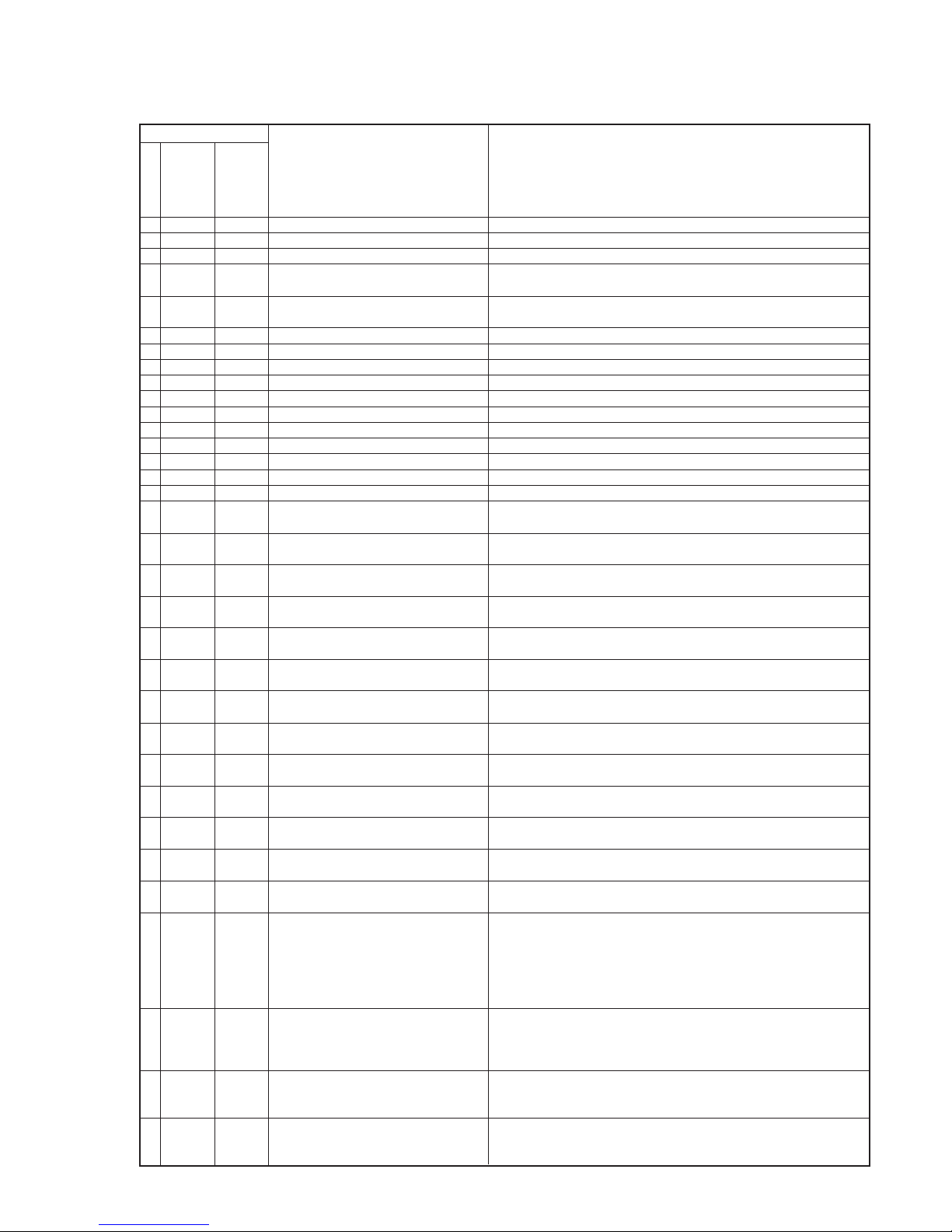
4. Self-diagnosis Code T able
Condensation.
Video head is dirty.
Non-standard battery is used.
LO AD direction. Loading does not
complete within specified time
UNLOAD direction. Loading does not
complete within specified time
T reel side tape slacking when unloading.
S reel side tape slacking when unloading.
T reel fault
S reel fault
FG fault when starting capstan
FG fault during normal capstan operations
FG fault when starting drum
PG fault when starting drum
FG fault during normal drum operations
PG fault during normal drum operations
Phase fault during normal drum operations
LO AD direction loading motor time-out
UNLOAD direction loading motor time-
out
T reel side tape slacking when unloading.
S reel side tape slacking when unloading.
T reel fault
S reel fault
FG fault when starting capstan
FG fault during normal capstan operations
FG fault when starting drum
PG fault when starting drum
FG fault during normal drum operations
PG fault during normal drum operations
Phase fault during normal drum operations
Difficult to adjust f ocus
(Cannot initialize focus.)
Zoom operations fault
(Cannot initialize zoom lens.)
Handshake correction function does not
work well.(With pitch angular velocity
sensor output stopped)
Handshake correction function does not
work well.(With y aw angular velocity
sensor output stopped)
Self-diagnosis Code
Repaired by:
Block
Function
Detailed
Code
Symptom/State Correction
C
C
C
C
C
C
C
C
C
C
C
C
C
C
C
C
C
C
C
C
C
C
C
C
C
C
C
C
C
E
E
E
E
21
22
23
31
31
31
31
31
31
31
31
31
31
31
31
31
32
32
32
32
32
32
32
32
32
32
32
32
32
61
61
62
62
00
00
00
10
11
20
21
22
23
30
31
40
41
42
43
44
10
11
20
21
22
23
30
31
40
41
42
43
44
00
10
00
01
Page 8

– 8 –
SERVICE NOTE
1. Power Supply During Repairs ......................................... 5
2. To Take out a Cassette when not Eject (Force Eject)....... 5
Self-Diagnosis Function
1. Self-diagnosis function ....................................................6
2. Self-diagnosis Display ..................................................... 6
3. Service Mode Display......................................................6
3-1. Display Method................................................................ 6
3-2. Switching of Backup No.................................................. 6
3-3. End of Display ................................................................. 6
4. Self-diagnosis Code Table ............................................... 7
1. GENERAL
Using this manual ......................................................................1-1
Checking supplied accessories ..................................................1-1
Installing and Charging the battery pack ...................................1-1
Inserting a cassette.....................................................................1-2
Camera recording ......................................................................1-2
Hints for better Shooting ...........................................................1-4
Checking the recorded picture ...................................................1-5
Playing back a tape ....................................................................1-5
Searching for the end of the picture ..........................................1-6
Using alternative power sources................................................1-6
Changing the mode settings ......................................................1-7
Shooting with backlighting .......................................................1-8
Using the FADER function .......................................................1-8
Shooting in the dark (NightShot) ..............................................1-9
Using the wide mode function...................................................1-9
Using the PROGRAM AE function...........................................1-9
Focusing manually...................................................................1-10
Enjoying picture effect ............................................................1-10
Adjusting the exposure ............................................................1-11
Superimposing a title ...............................................................1-11
Making your own titles............................................................1-12
Recording with the date/time...................................................1-12
Optimizing the recording condition.........................................1-12
Releasing the STEADY SHOT function .................................1-13
Watching on a TV screen.........................................................1-13
Editing onto another tape.........................................................1-13
Recording from a VCR or TV .................................................1-14
Changing the lithium battery in the camcoder ........................1-14
Resetting the date and time......................................................1-14
Simple setting of clock by time difference..............................1-15
Usable cassettes and playback modes .....................................1-15
Tips for using the battery pack ................................................1-15
Maintenance information and precautions ..............................1-16
Using your camcorder abroad .................................................1-17
Self-diagnosis display..............................................................1-17
Identifying the parts.................................................................1-18
Warning Indicators ..................................................................1-20
TABLE OF CONTENTS
2. DISASSEMBLY
2-1. Removal of Front Panel Block .........................................2-1
2-2. Removal of Cabinet (R) Block .........................................2-2
2-3. Removal of EVF Block-1................................................. 2-2
2-4. Removal of LCD Block (3/3.5 inch) ................................2-2
2-5. Removal of LCD Block (2.5 inch) ...................................2-2
2-6. Remov al of CF-51 (CF-50) Board and Control Switch Block
(MR-8500)/(MF-8500) .................................................... 2-3
2-7. Removal of EVF Block-2................................................. 2-3
2-8. Removal of Cabinet (L) Block and
Battery Panel Block .........................................................2-4
2-9. Removal of Cassette Lid Assembly .................................2-4
2-10. Removal of Control Switch Block (FK-8500) .................2-4
2-11. Removal of Zoom Lens Block .........................................2-5
2-12. Removal of DD-105 Board and PJ-84 (PJ-83) Board......2-5
2-13. Removal of VC-195 and SE-67 (SE-66) Board ............... 2-5
2-14. Service Position ............................................................... 2-6
2-15. Circuit Board Location..................................................... 2-7
3. BLOCK DIAGRAMS
3-1. Overall Block Diagram ....................................................3-1
3-2. Camera/Video 1 Block Diagram ......................................3-5
3-3. VTR/Camera Control Block Diagram .............................3-9
3-4. Servo Block Diagram .....................................................3-12
3-5. Mode Control Block Diagram........................................3-15
3-6. Audio Block Diagram ....................................................3-19
3-7. LCD (CCD-TR V23E/TRV45E/TRV55E/TRV65E/TRV69E/
TR V75/TR V75PK/TRV715) Block Diagram ......................3-23
3-8. LCD (CCD-TR V3E/TRV13E) Block Diagram ...................3-26
3-9. B/W EVF Block Diagram ..............................................3-29
3-10. Power Block Diagram ....................................................3-33
Page 9

– 9 –
4. PRINTED WIRING BOARDS AND SCHEMATIC
DIAGRAMS
4-1. Frame Schematic Diagram (1) ...........................................4-1
• Frame Schematic Diagram (2) ........................................4-4
4-2. Printed Wiring Boards and Schematic Diagrams...............4-7
• CD-197/198 (CCD Imager)
(2.5 Inch LCD, 3 Inch/3.5 Inch LCD Model) Board.......4-8
• VC-195 (Camera, Y/C Processor, IN/OUT,
REC/PB Head Amp, Servo/System Control, Servo,
Audio, IR Transmiter, Mode Control) Board ................4-10
• VC-195 (Camera 1) Board ............................................4-17
• VC-195 (Camera 2) Board ............................................4-19
• VC-195 (Y/C Process) Board........................................4-23
• VC-195 (IN/OUT) Board ..............................................4-27
• VC-195 (REC/PB Head Amp) Board............................4-31
• VC-195 (Servo/System Control) Board ........................4-35
• VC-195 (Servo) Board ..................................................4-38
• VC-195 (Audio) Board..................................................4-41
• VC-195 (IR Transmiter) Board .....................................4-46
• VC-195 (Mode Control) Board .....................................4-49
• SE-67/66 (Steady Shot)
(2.5 Inch, 3 Inch/3.5 Inch LCD Model) Board..............4-52
• PJ-83/84 (AV IN/OUT)
(2.5 Inch, 3 Inch/3.5 Inch LCD Model) Board..............4-55
• MA-331 (Stereo Mic, Laser Link)
(2.5 Inch LCD Model) Board ........................................4-58
• MA-312 (Stereo Mic, Laser Link)
(3 Inch/3.5 Inch LCD Model) Board.............................4-59
• CF-50 (Control (2.5 Inch LCD Model)) Board .............4-64
• CF-51 (Control (3 Inch/3.5 Inch LCD Model)) Board..4-73
• Control Switch Block (FK-8500/SS-8500) ...................4-77
• PD-92 (RGB Decorder, LCD Drive, Back Light LCD
(2.5 Inch LCD Model)) Board.......................................4-78
• PD-92 (RGB Decorder) Board ......................................4-81
• PD-92 (LCD Drive) Board ............................................4-84
• PD-92 (Back Light) Board ............................................4-87
• PD-92 (LCD) Board ......................................................4-88
• PD-93 (RGB Decorder, LCD Drive, Back Light LCD
(3 Inch/3.5 Inch LCD Model)) Board ...........................4-90
• PD-93 (RGB Decorder) Board ......................................4-93
• PD-93 (LCD Drive) Board ............................................4-96
• PD-93 (Back Light) Board ............................................4-99
• PD-93 (LCD) Board ....................................................4-100
• VF-99 (B/W EVF (B/W EVF Model)) Board.............4-103
• DD-105 (Power) Board ...............................................4-108
5. ADJUSTMENTS
5-1. CAMERA SECTION ADJUSTMENTS ..........................5-1
1-1. Preparations before Adjustment (Camera Section) ..........5-1
1-1-1. List of Service Tools ................................................. 5-1
1-1-2. Preparations ...............................................................5-2
1-1-3. Precautions ................................................................5-5
1. Setting the Switch .....................................................5-5
2. Adjusting Procedure ..................................................5-5
3. Subject .......................................................................5-5
1-1-4. Adjusting Remote Commander .................................5-6
1. Using the adjusting remote commander ....................5-6
2. Precautions upon using the adjusting
remote commander ....................................................5-6
1-1-5. Data Processing .........................................................5-7
1-2. Initialization of D, E, F Page Data....................................5-8
1. Initialization of D, E, F Page Data ............................5-8
2. Modification of D, E, F Page Data...........................5-8
3. D Page Table .............................................................5-9
4. F Page Table ............................................................5-10
5. E Page Table ............................................................5-12
1-3. Camera System Adjustments .......................................... 5-14
1. G-CAM flip Adjustment ......................................... 5-14
2. Hall Adjustment ......................................................5-15
3. Flange Back Adjustment .........................................5-16
3-1. Flange Back Adjustment (1) ................................... 5-16
3-2. Flange Back Adjustment (2) ................................... 5-16
4. Flange Back Check .................................................5-17
5. Picture Frame Setting ..............................................5-17
6. Color Reproduction Adjustment ............................. 5-18
7. IRIS IN/OUT Adjustment .......................................5-19
8. MAX GAIN Adjustment .........................................5-19
9. Auto White Balance Standard Data Input ...............5-20
10. Auto White Balance Adjustment.............................5-20
11. White Balance Check ..............................................5-21
12. Angular Velocity Sensor Sensitivity Adjustment ....5-22
(CCD-TRV45E/TRV55E/TRV65E/TRV69E/TRV75/
TRV75PK/TRV715)
1-4. Monochrome Electronic Viewfinder
System Adjustments .......................................................5-23
1-4-1. Horizontal Slant Check ...........................................5-23
1-4-2. Centering Adjustment ............................................. 5-23
1-4-3. Focus Adjustment ....................................................5-23
1-4-4. Aberration Adjustment ............................................5-24
1-4-5. Horizontal Amplitude Adjustment (VF-99 board) ..5-24
1-4-6. Vertical Amplitude Adjustment (VF-99 board)....... 5-25
1-4-7. Brightness Adjustments (VF-99 board) ..................5-25
1-4-8. Horizontal Amplitude, Vertical Amplitude,
Focus Check ............................................................5-25
1-5. LCD System Adjustment ................................................ 5-26
1. LCD initial data input ............................................. 5-26
2. VCO adjustment (PD-92/93 board) ........................ 5-27
3. D range adjustment (PD-92/93 board) ....................5-27
4. Bright adjustment (PD-92/93 board).......................5-28
5. Contrast adjustment (PD-92/93 board) ...................5-28
6. V-COM level adjustment (PD-92/93 board) ........... 5-29
7. Color adjustment (PD-92/93 board) ........................5-29
8. V-COM adjustment (PD-92/93 board)....................5-30
9. White balance adjustment (PD-92/93 board) ..........5-30
5-2. MECHANICAL SECTION ADJUSTMENT .................5-31
2-1. Operating without a Cassette ..........................................5-31
2-2. Tape path Adjustment .....................................................5-31
1. Preparations for adjustments ...................................5-31
Page 10

– 10 –
5-3. VIDEO SECTION ADJUSTMENTS.............................5-32
3-1. Preparations before Adjustment..............................5-32
3-1-1. Equipments to be Used ...........................................5-32
3-1-2. Precautions on Adjusting ........................................5-33
3-1-3. Adjusting Connectors..............................................5-33
3-1-4. Connecting the Equipments ....................................5-34
3-1-5. Alignment T ape .......................................................5-34
3-1-6. Input/Output Level and Impedance.........................5-36
3-1-7. Recording Mode (Standard 8/Hi8) switching
(Hi8 model) .............................................................5-36
3-1-8. Service Mode ..........................................................5-36
1. Test mode setting.....................................................5-36
2. Emergency memory address ...................................5-37
2-1. EMG CODE (Emergency Code) .............................5-37
2-2. MSW Codes ............................................................5-38
3. Bit value discrimination ..........................................5-39
4. Switch check (1)......................................................5-39
5. Switch check (2)......................................................5-40
6. Headphone jack check ............................................5-40
7. Input/output selection check ...................................5-40
8. LED, LCD (display window) check........................5-41
9. Record of use check ................................................5-41
3-2. System Control System Adjustment .......................5-42
1. Initialization of D, E, F Page Data ..........................5-42
2. Battery End Adjustment (VC-195 board) ...............5-42
3-3. Servo System Adjustments ......................................5-43
1. CAP FG Offset Adjustment (VC-195 board)..........5-43
2. Switching Position Adjustment (VC-195 board) ....5-43
3. NTSC LP Mode Switching Position Adjustment
(VC-195 board) (CCD-TR V75/TR V75PK/TRV715)....5-44
3-4. Video System Adjustments .....................................5-44
1. 28 MHz Origin Oscillation Adjustment
(VC-195 board) .......................................................5-44
2. AFC f0 Adjustment (VC-195 board) ...................... 5-45
3. Filter f0 Adjustment (VC-195 board)...................... 5-45
4. Y OUT Level Adjustment (VC-195 board) .............5-46
5. C OUT Level Adjustment (VC-195 board) .............5-46
6. RP Filter f0 Adjustment (VC-195 board)................5-47
7. Hi8 REC Y Current Adjustment
(VC-195 board) (CCD-TRV65E/TRV69E/TRV75/
TRV75PK/TRV715)................................................5-48
8. Standerd8 REC Y Current Adjustment
(VC-195 board) (CCD-TRV3E/TRV13E/TRV23E/
TRV45E/TRV55E) ..................................................5-49
9. Hi8 REC L Level Adjustment
(VC-195 board) (CCD-TRV65E/TRV69E/TRV75/
TRV75PK/TRV715)................................................5-50
10. Standerd8 REC L Level Adjustment
(VC-195 board) (CCD-TRV3E/TRV13E/TRV23E/
TRV45E/TRV55E) ..................................................5-51
11. REC C Current Adjustment (VC-195 board) ..........5-52
3-5. IR Transmitter Adjustments
(CCD-TRV75/TRV75PK/TR V715) ........................5-53
1. IR Video Carrier Frequency Adjustment
(VC-195 board) .......................................................5-53
2. IR Video Deviation Adjustment (VC-195 board)....5-53
3. IR Audio Deviation Adjustment (VC-195 board) ...5-54
3-6. Stereo Audio System Adjustment
(CCD-TR V45E/TR V55E/TR V65E/TR V69E/TRV75/
TR V75PK/TR V715)................................................5-55
1. 1.5 MHz Deviation Adjustment (VC-195 board)....5-57
2. 1.7 MHz Deviation Adjustment (VC-195 board)....5-57
3. BPF f0 Adjustment (VC-195 board) .......................5-58
3-7. Monaural Audio System Adjustment
(CCD-TR V3E/TR V13E/TR V23E) ..........................5-58
1. 1.5 MHz Deviation Adjustment (VC-195 board)....5-59
2. BPF Adjustment (VC-195 board) ...........................5-59
3-8. Arrangement Diagram for Adjustment Parts ...........5-60
6. REPAIR P ARTS LIST
6-1. Exploded Vie ws ....................................................... 6-1
6-1-1. Cabinet (L) Block Assembly....................................6-1
6-1-2. Front Panel Block Assembly....................................6-2
6-1-3. Cabinet (R) Block Assembly
(TRV45E/TRV55E/TRV75/TRV75PK/TRV715) ....6-3
6-1-4. Cabinet (R) Block Assembly
(TRV3E/TRV13E/TRV23E/TRV65E/TRV69E)......6-4
6-1-5. LCD Block Assembly (3/3.5 Inch)
(TRV45E/TRV55E/TRV75/TRV75PK/TRV715) ....6-5
6-1-6. LCD Block Assembly (2.5 Inch)
(TRV3E/TRV13E/TRV23E/TRV65E/TRV69E)......6-6
6-1-7. EVF Block Assembly (B/W EVF) ...........................6-7
6-1-8. Main Boards Assembly ............................................6-8
6-1-9. Battery Panel and CCD Block Assembly ................6-9
6-1-10. Device Lens (LSV-600A/LSV-601A) ....................6-10
6-1-11. Cassette Compartment Assembly ..........................6-11
6-1-12. LS Chassis Assembly............................................. 6-12
6-1-13. Mechanism Chassis Assembly............................... 6-13
6-2. Electrical Parts List ................................................6-14
Page 11
Page 12
Page 13
Page 14
Page 15
Page 16
Page 17
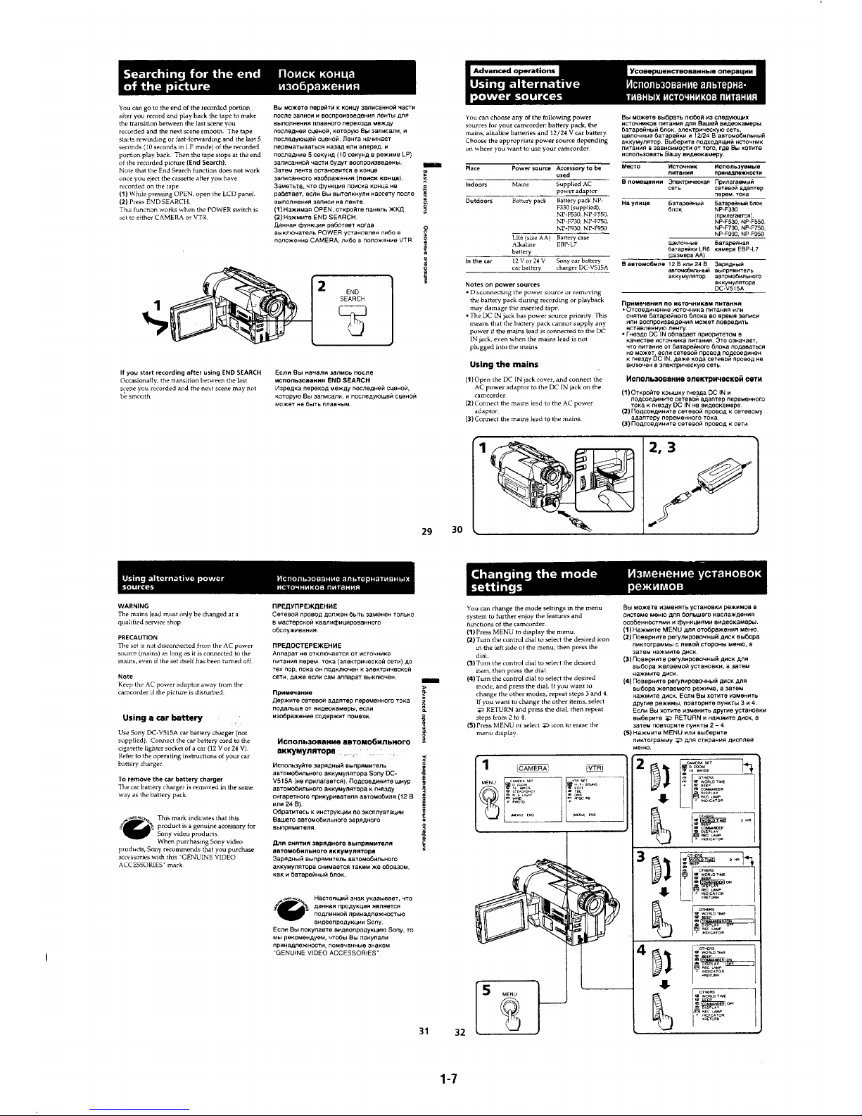
Page 18
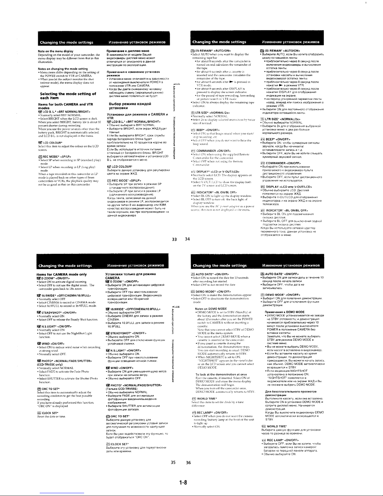
Page 19
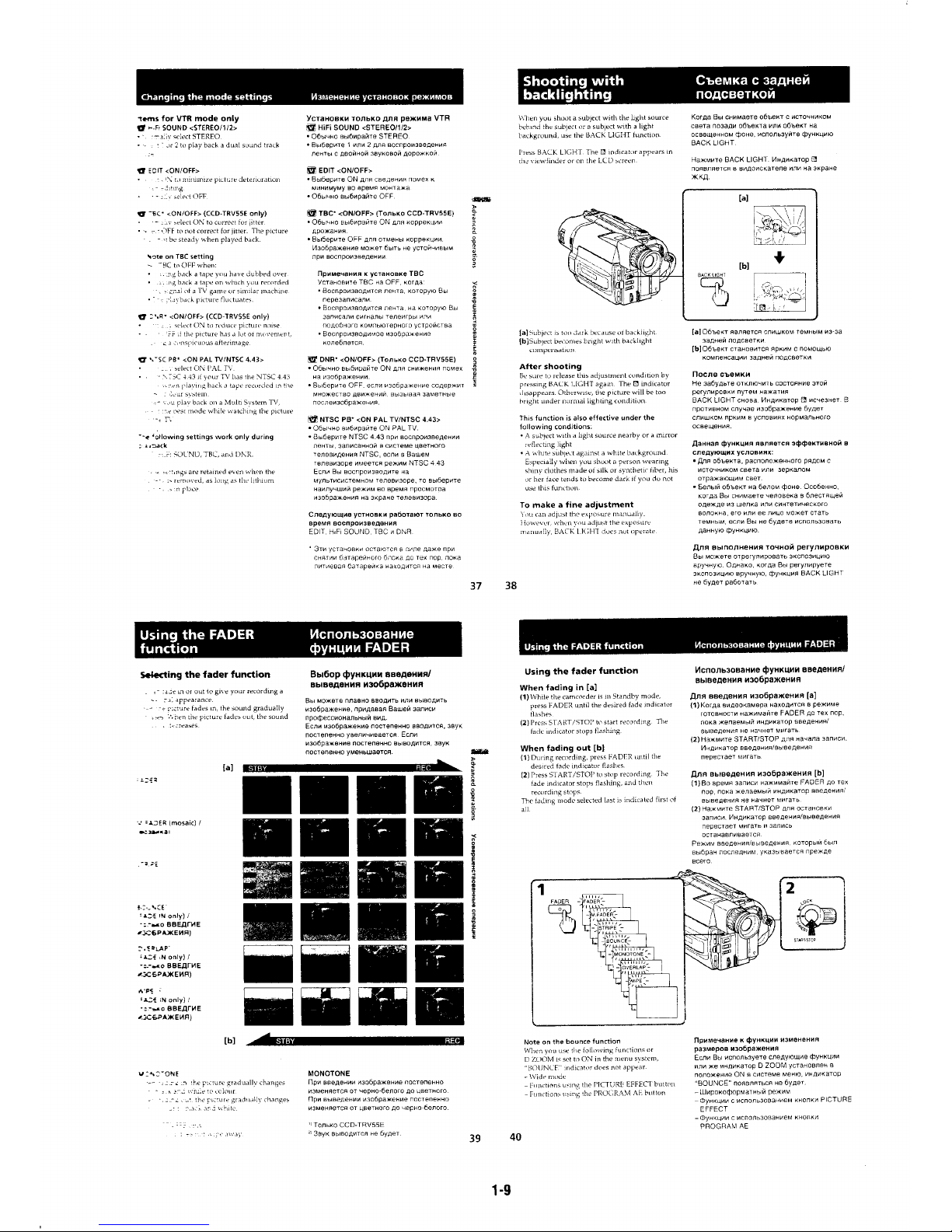
Page 20
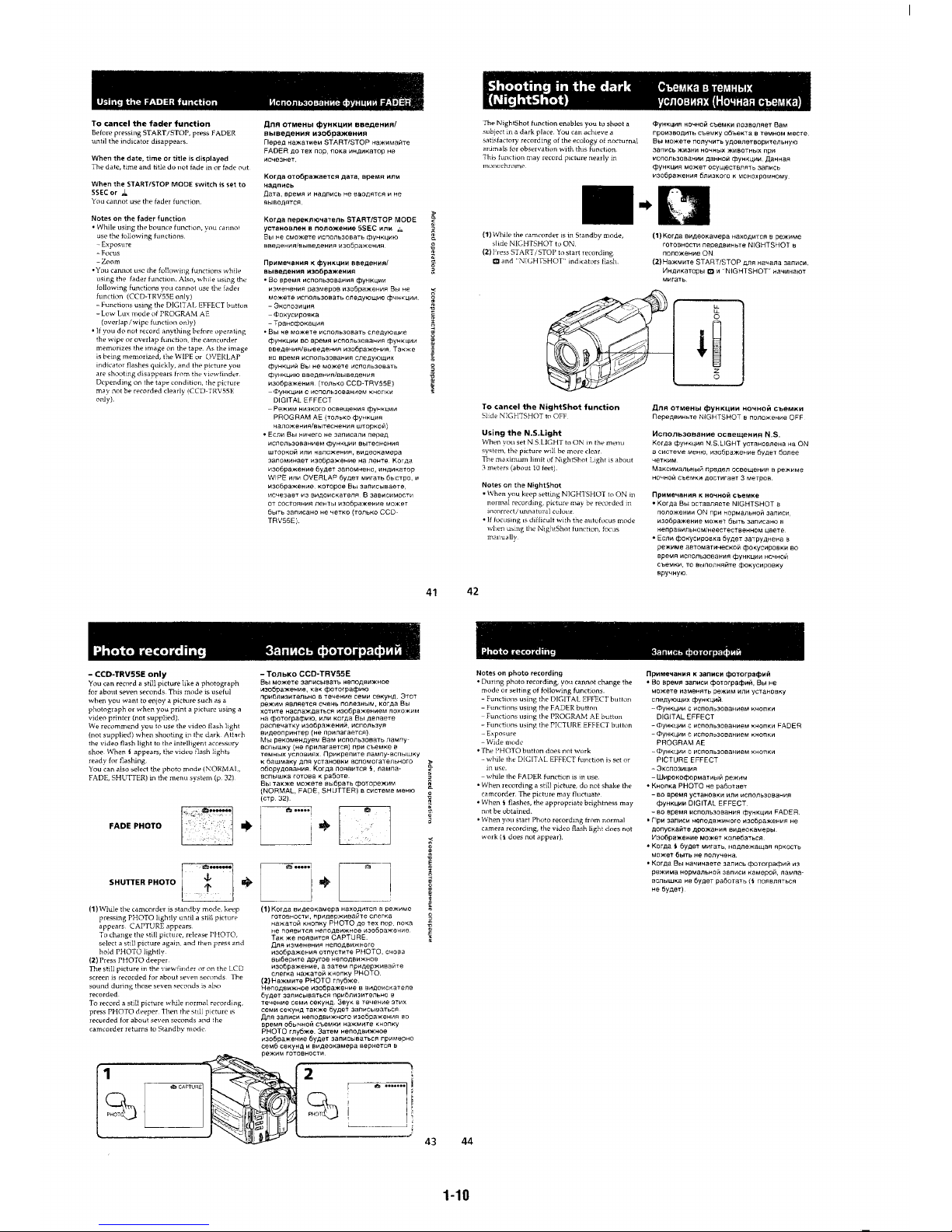
Page 21
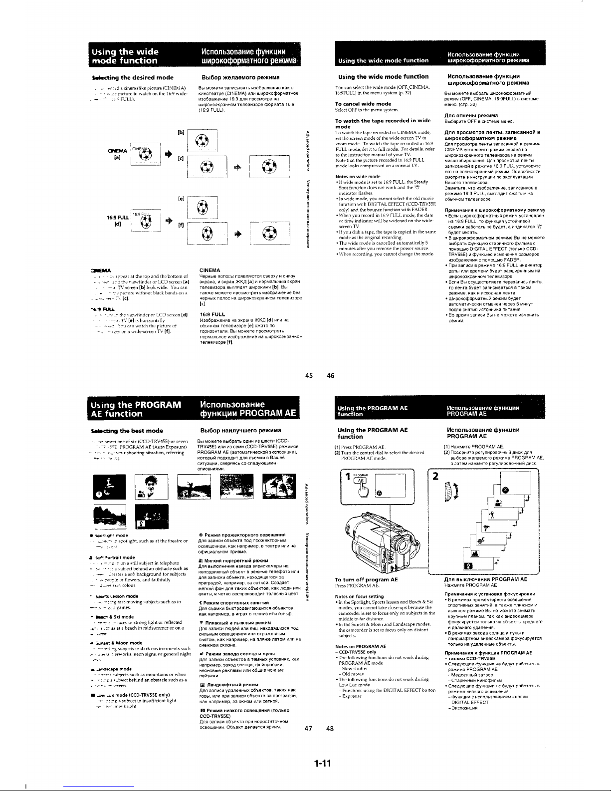
Page 22
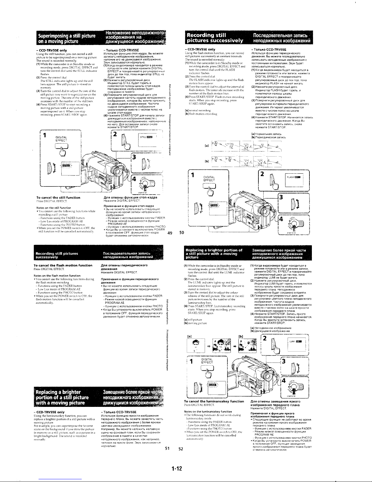
Page 23
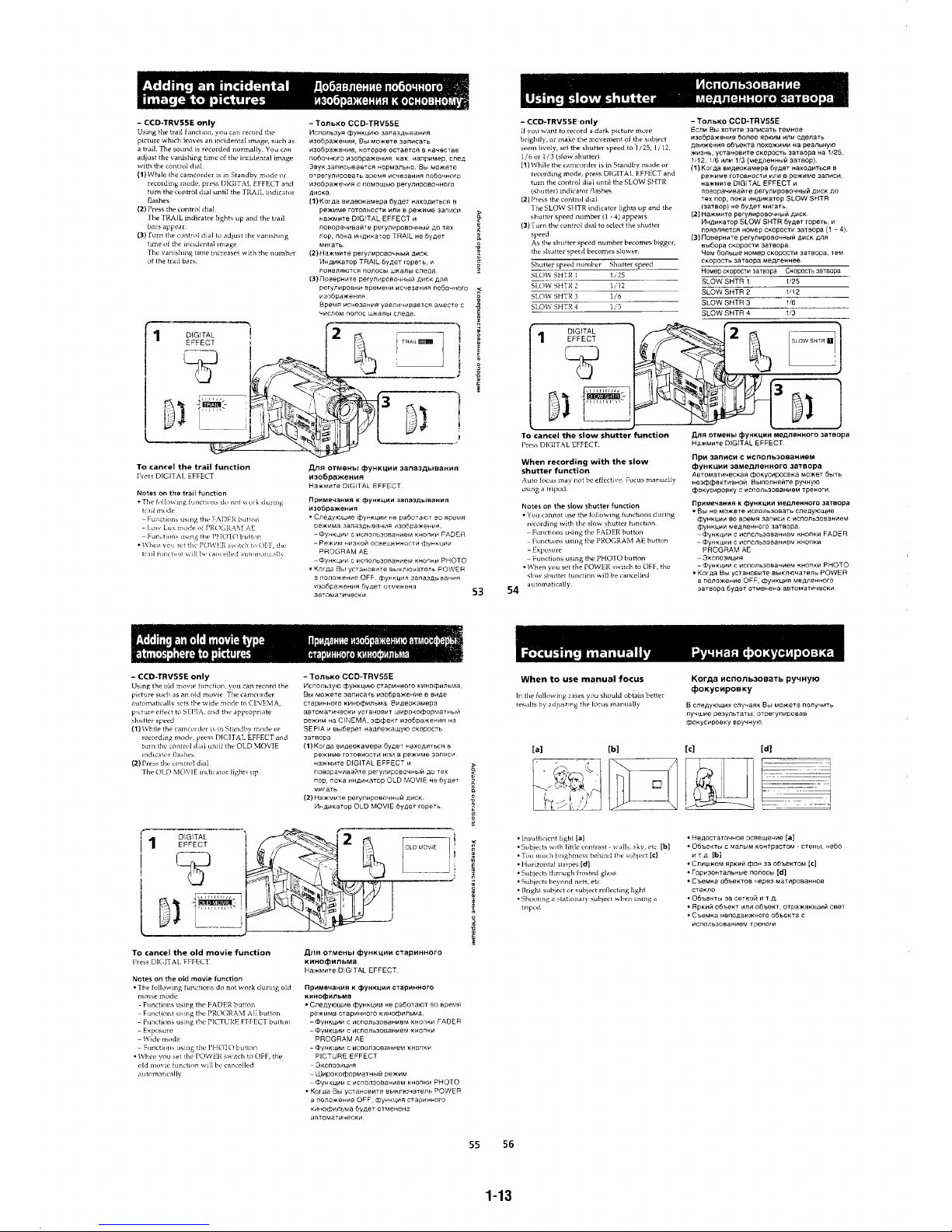
Page 24
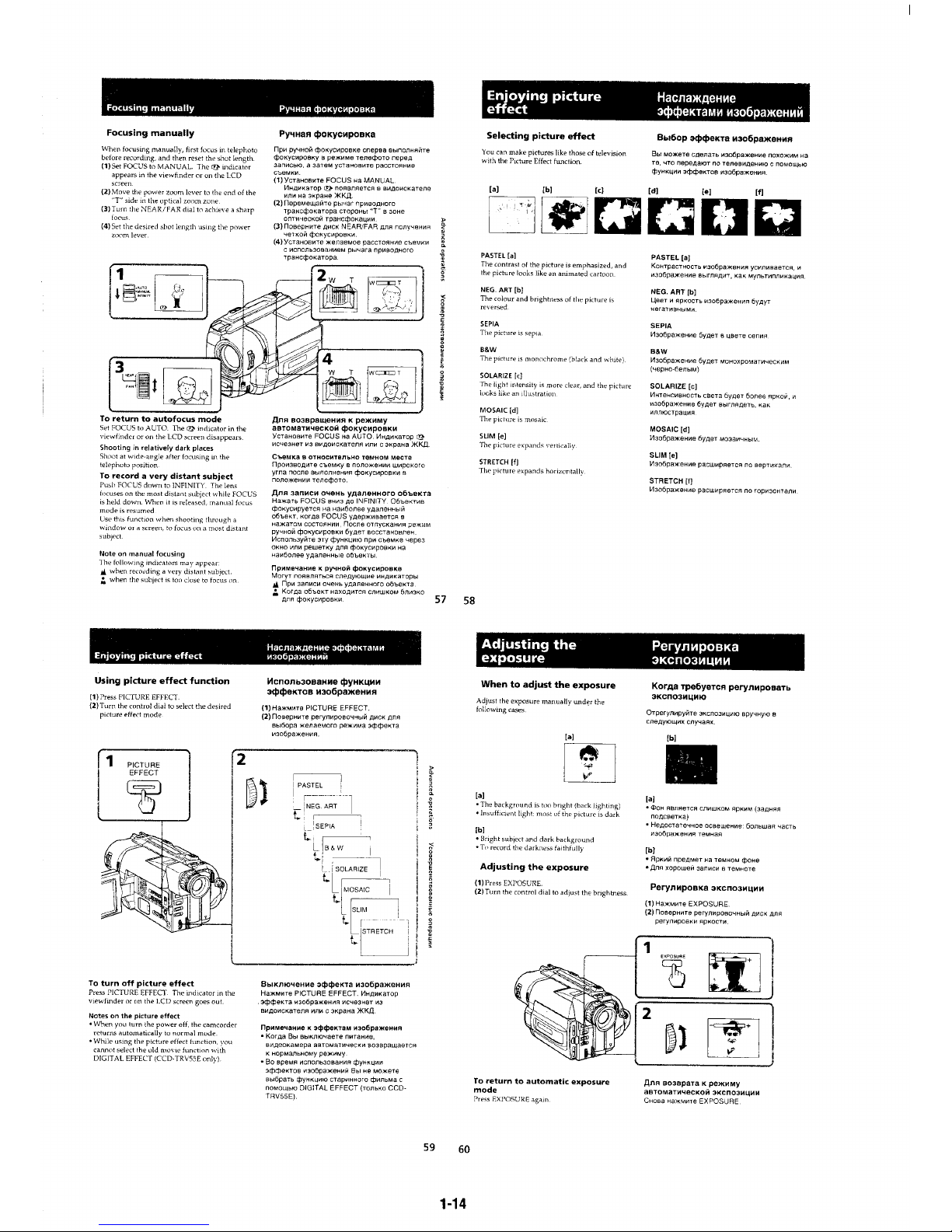
Page 25
Page 26
Page 27
Page 28
Page 29
Page 30
Page 31
Page 32
Page 33
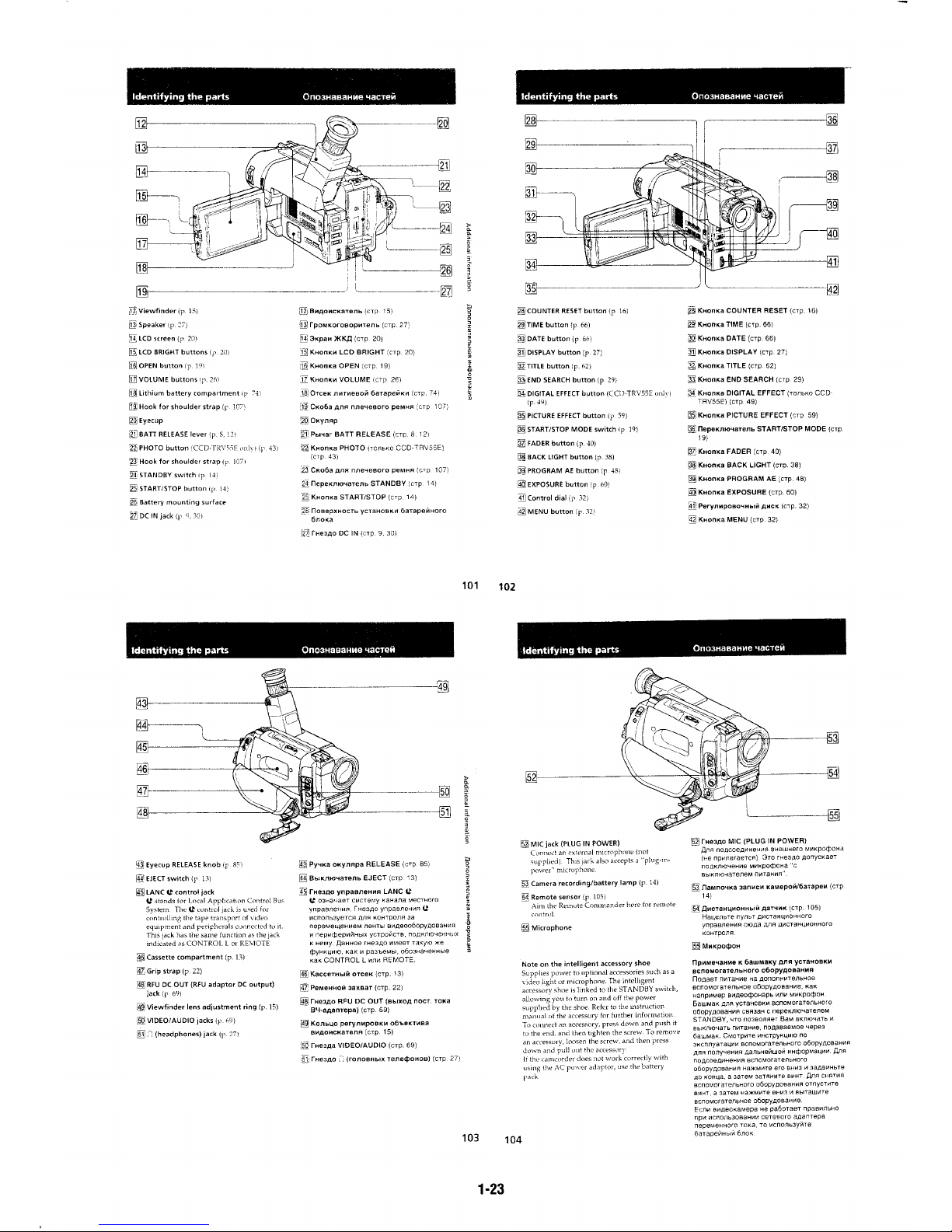
Page 34
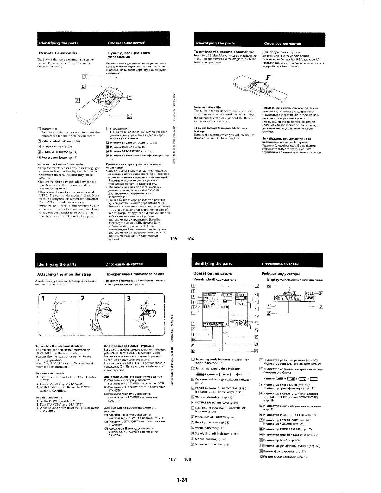
Page 35
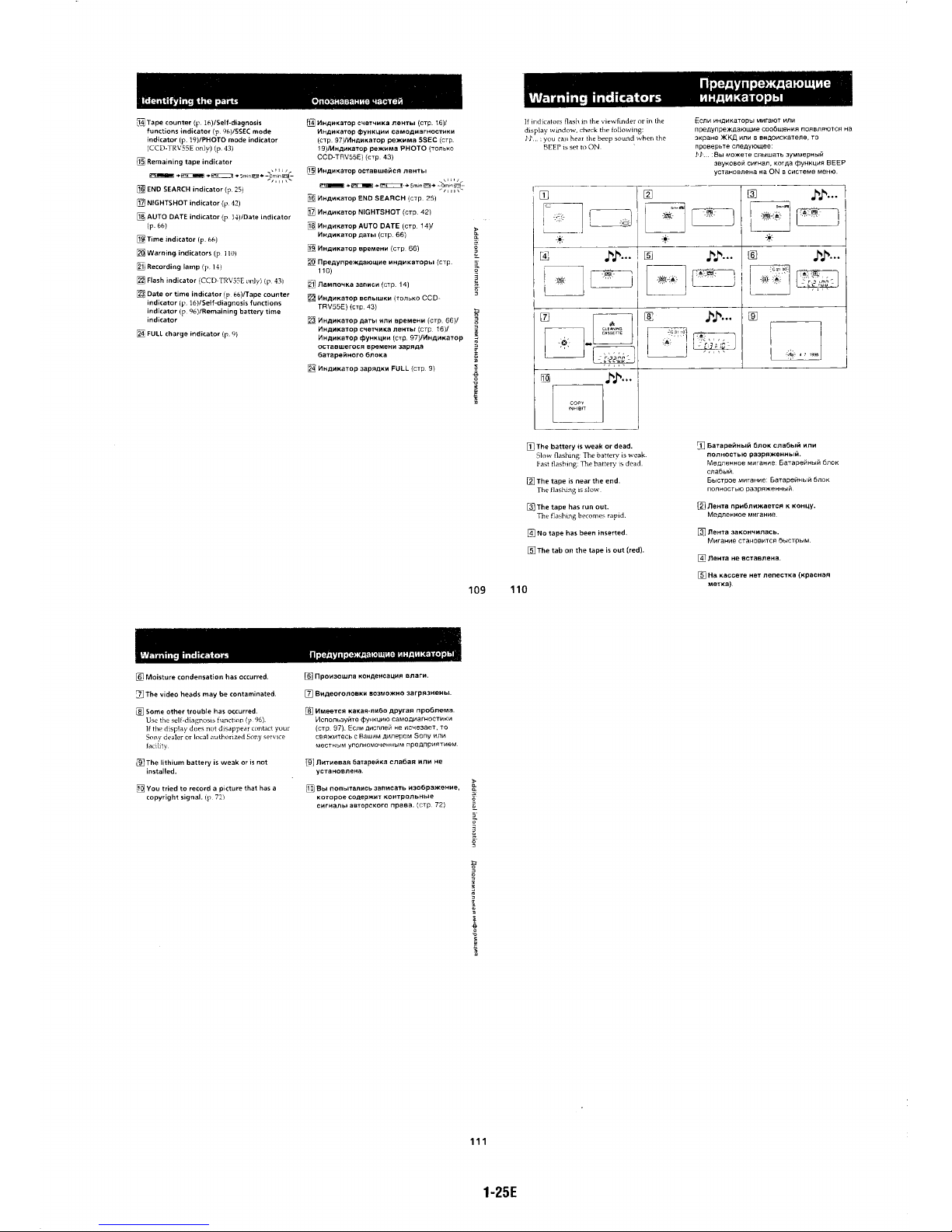
Page 36
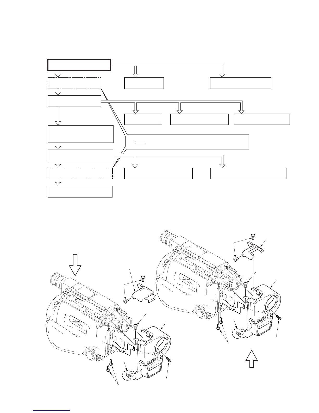
2-1
SECTION 2
DISASSEMBLY
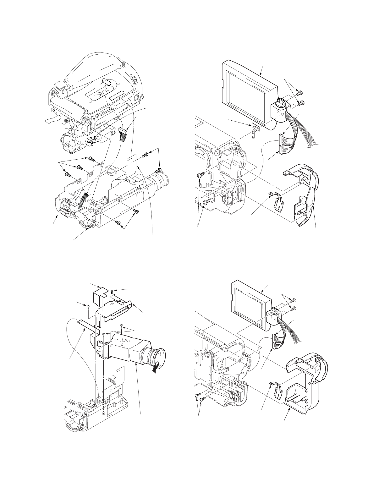
2-1. REMOVAL OF FRONT PANEL BLOCK
The equipment can be removed using the following procedure.
NOTE : Follow the disassembly procedure in the numerical order given.
CCD-TRV3E/TRV13E/TRV23E/TRV45E/TRV55E/TRV65E/
TRV69E/TRV75/TRV75PK/TRV715
VIDEO CAMERA RECORDER
2-1. FRONT PANEL BLOCK
2-7. EVF BLOCK-2
(VF-99 BOARD)
2-2. CABINET (R) BLOCK
2-8. CABINET (L) AND BATTERY
PANEL BLOCK
2-6. CF-51 (CF-50) BOARD AND
CONTROL SWITCH BLOCK
(MR-8500) / (MF-8500)
2-10. CONTROL SWITCH BLOCK
(FK-8500)
2-11. ZOOM LENS BLOCK
2-13. VC-195/SE-67 (SE-66)
BOARDS
2-3. EVF BLOCK-1 2-4.LCD BLOCK (3-3.5INCH) 2-5.LCD BLOCK (2.5INCH)
2-9. CASSETTE LID ASSEMBLY
2-12. DD-105/PJ-84 (PJ-83) BOARDS
The means that each model has different operating procedure.
7
FP-629 flexible board
CN303, 20P
1
Two screws (M2x4)
5
Two screws (M2x4)
3
Screw (M2x4)
4
Screw (M2x4)
2
Cabinet (S)
Claw
6
Front panel bloc
k
EXCEPT TRV3E/TRV13E
TRV3E/TRV13E
7
FP-629 flexible board
CN303, 20P
1
Two screws (M2x4)
5
Two screws (M2x4)
3
Screw (M2x4)
4
Screw (M2x4)
2
Cabinet (N)
Claw
6
Front panel block
Page 37
2-2
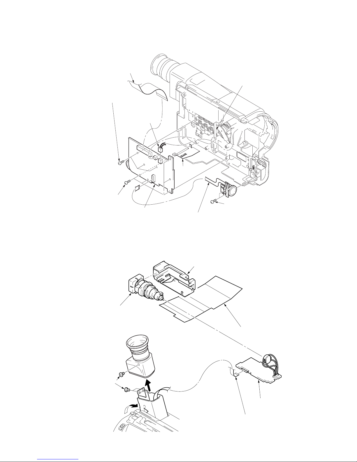
2-2. REMOVAL OF CABINET (R) BLOCK
2-3. REMOVAL OF EVF BLOCK-1
2-4. REMOVAL OF LCD BLOCK (3/3.5 INCH)
2-5. REMOVAL OF LCD BLOCK (2.5 INCH)
1
Two screws (M2x4)
2
Two screws
(M2x4)
6
Connector
CN933,11P
Pin
5
Flat cable (FFC-236)
CN001, 50P
4
Cabinet (R) block
3
Three screws
(M2x4)
Hole (Night shot lever)
5
VF base
3
Tapping screw
4
Tapping screw
7
Three
tapping screw
6
Tilt-up the EVF block
to the direction of arrow.
2
VF flexible retainer sheet
1
Flate cable(FCC-235)
CN008,4P
4
Connector
CN006,6P
6
Four tapping screws
7
LCD block
8
Hinge ground plate
1
Five tapping screws
3
IR knob
2
IR cover
5
Connector
CN005,12P
4
Connector
CN006,6P
6
Four tapping screws
7
LCD block
1
Five tapping screws
3
IR knob
2
IR cover
5
Connector
CN005,12P
Page 38
2-3
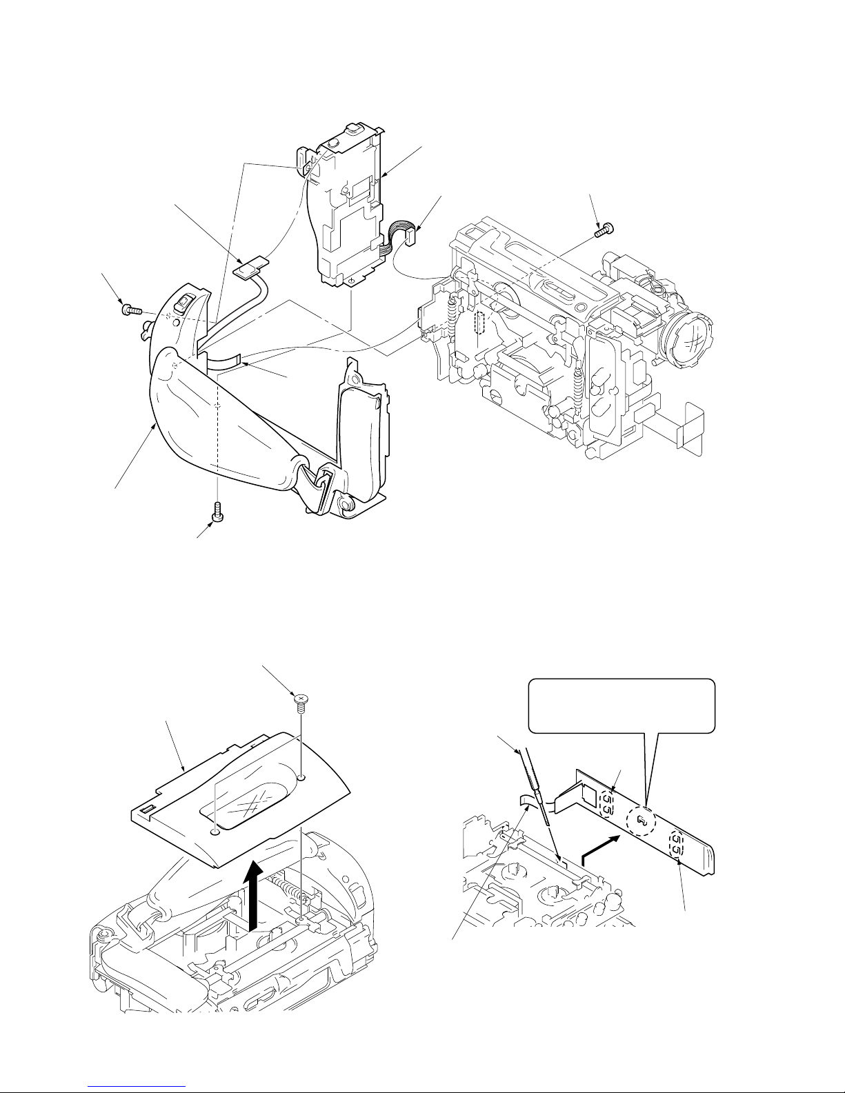
2-6. REMOVAL OF CF-51 (CF-50) BOARD AND
CONTOROL SWITCH BLOCK (MR-8500)/(MF-
8500)
2
Control switch block (MF-8500)
CN002,8P (Manual focus model)
(CCD-TRV45E/TRV55E/TRV75/TRV75PK/TRV715 only)
2
Control switch block (MR-8500)
CN002,8P (Manual focus model)
(CCD-TRV23E/TRV65E/TRV769E only)
3
Five tapping
screws
5
CF-50 board (2.5 inch model)
5
CF-51 board (3/3.5 inch model)
1
Two tapping
screws
6
Ground
plate
4
Three tapping
screws
7
Connector
CN003,2P
8
Flat cable (FFC-236)
CN001, 50P
9
Flate cable (FCC-235)
CN008,4P
2-7. REMOVAL OF EVF BLOCK-2
8
VF-99 board
7
CRT assembly
6
CRT holder assmebly
4
VF electrostatic sheet
1
Tilt-up the EVF block to the direction of arrow A.
5
Flexible flat cable(FCC-235
)
CN901,4P
2
Three screws (M2x3)
3
Remove the EVF rear cabinet assembly
to the direction of arrow
B
.
A
B
Page 39
2-4
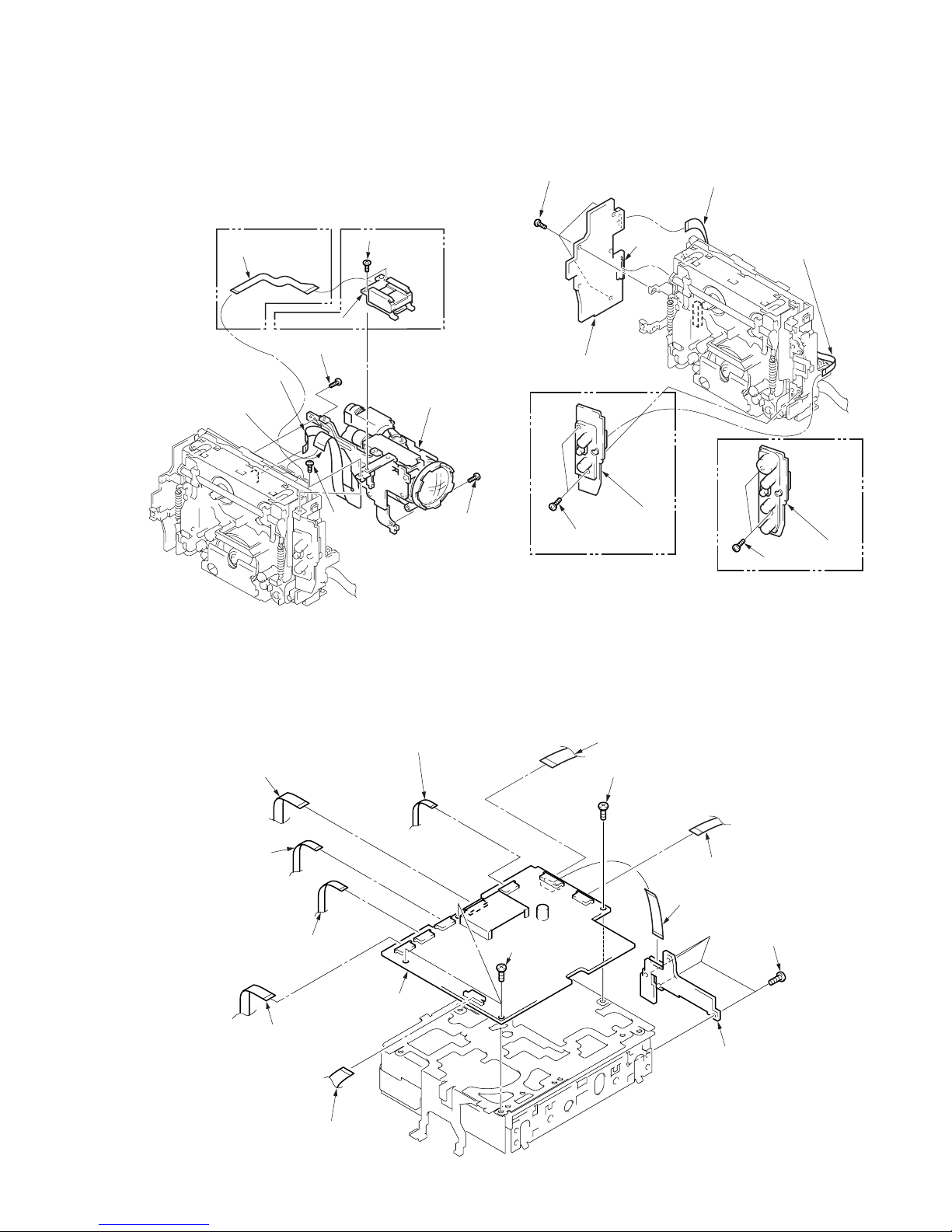
2-8. REMOVAL OF CABINET (L) BLOCK AND BATTERY PANEL BLOCK
2-9. REMOVAL OF CASSETTE LID ASSEMBLY 2-10. REMOVAL OF CONTROL SWITCH BLOCK
(FK-8500)
7
Cabinet(L)block
8
Flexible connector
CN934,12P
2
Screw (M2x4)
6
Screw (M2x3)
4
Battery panel block
1
Connector
CN801,7P
3
Screw (M2x4)
5
Control switch block
Two claws
Two claws
Screwdriver(
-
)
1
Remove the Control switch block
(FK-8500) in the direction of arrow
with pushing the claw.
2
Flexible connector
CN935, 10P
1
Two screws (M2x4)
2
Cassette lid assembly
Page 40
2-5
2-11. REMOV AL OF ZOOM LENS BLOCK 2-12. REMOVAL OF DD-105 BOARD AND
PJ-84 (PJ-83) BOARD
5
FP-623 flexible board
CN501, 16P
6
Lens flexible board
CN551, 23P
4
Zoom lens block
7
Two screws
(M2x3)
8
Shoe bracket
9
FP-633
flexible board
3
Screw (M2x3)
1
Screw
(M2x3)
2
Screw
(M2x3
)
Normal Accessory shoe : CCD-TRV23E
Inteligent Accessory shoe : CCD-TRV45E/
TRV55E/TRV65E/TRV69E/TRV75/TRV75PK/
TRV715
Normal Accssory
shoe
Inteligent Accssory
shoe
1
FP-622 flexible board
CN932,16P
4
FP-621 flexible board
CN902,12P
2
Three screws (M2 x 3)
5
Two screws (M2 x 4)
5
Two screws (M2 x 4)
3
DD-105 board
6
PJ-84 board
6
PJ-83 board
CN931,48P
CCD-TRV3E/TRV13E/
TRV23E
EXCEPT CCD-TRV3E/
TRV13E/TRV23E
2-13. REMOV AL OF VC-195 AND SE-67 (SE-66) BOARD
1
FP-220 flexible board
CN105, 8P from loading motor
7
FP-629 flexible board
8
FP-621 flexible board
CN902,12P
9
FP-620 flexible board
CN904,10P
6
FP-622 flexible board
CN912,16P
5
FP-221 flexible board
CN102, 15P
4
FP-248 flexible board
CN103, 12P
3
Flexible board
CN104, 10P
from drum motor
2
Flexible board
CN101, 16P
from video head
!¡
Screw (M2x3)
!º
Three screws (M2x3)
!£
Four screws (M2x3)
!¢
SE-67/SE-66 board
!™
VC-195 board
Page 41
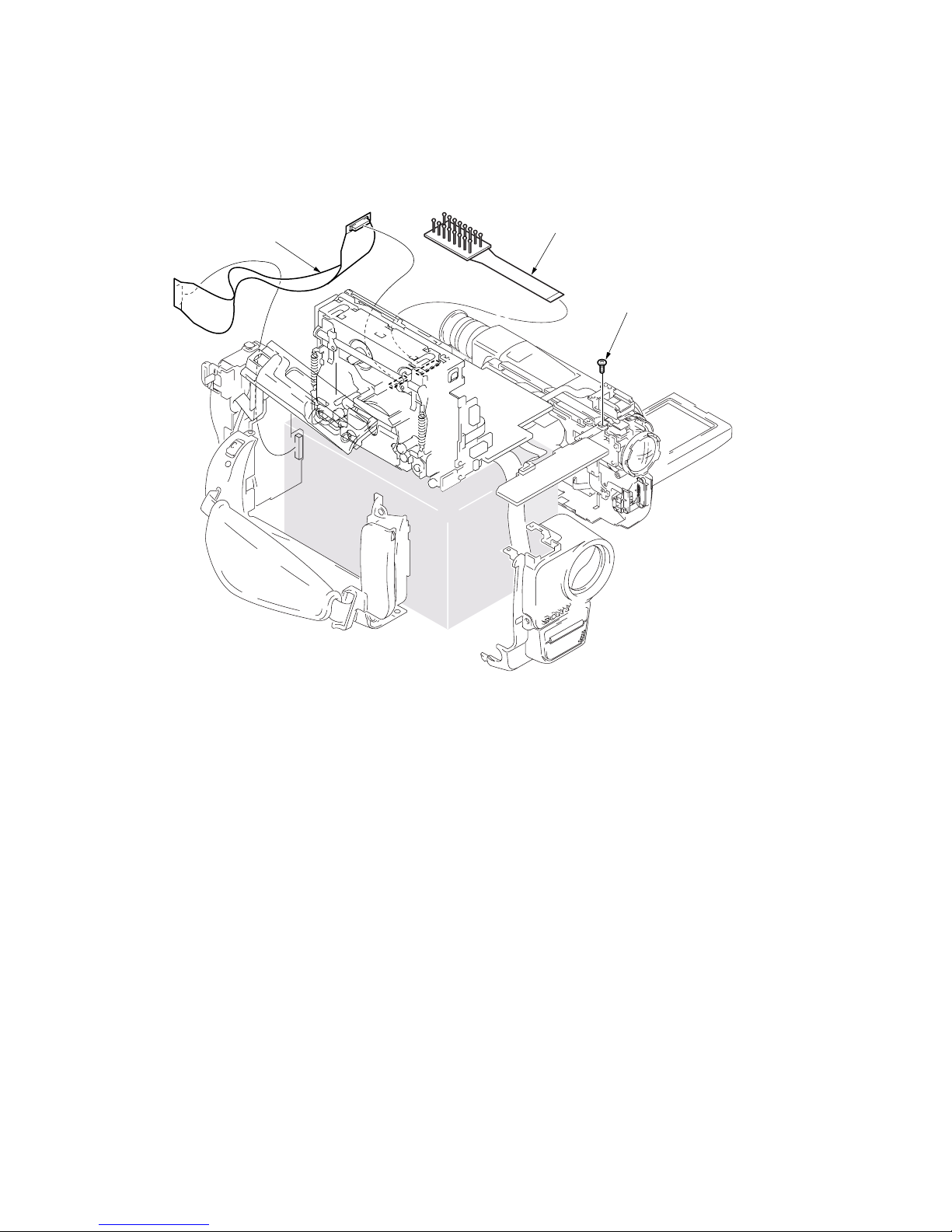
2-6
2-14. SERVICE POSITION
PREPARATION; Refer to the previous section “DISASSEMBLY”, and connect as shown in the figure after each parts has been removed.
Screw(M2x4)
J-6082-188-A
EXTENSION CORD
J-6082-382-A
CPC-7 Jig
Page 42
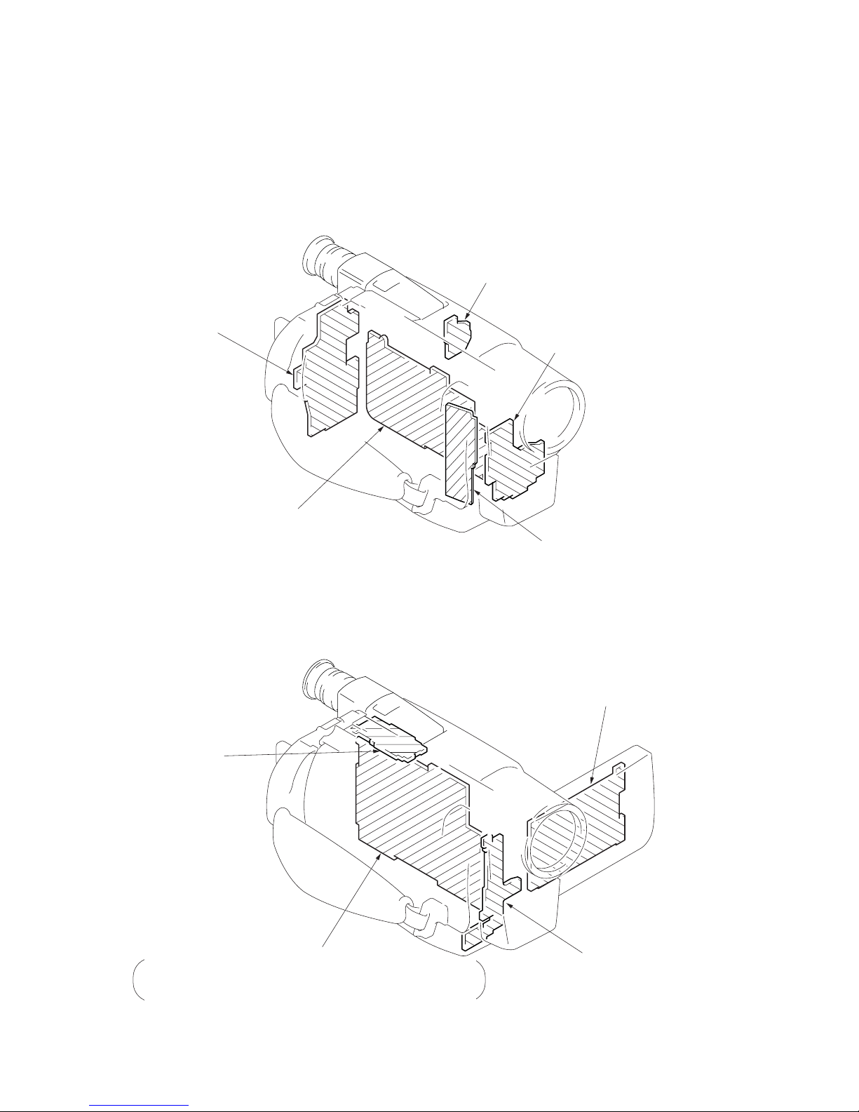
2-7
2-15. CIRCUIT BOARDS LOCATION
2.5 INCH LCD MODEL : CCD-TRV3E/TRV13E/TRV23E/
TRV65E/TRV69E
3 INCH LCD MODEL : CCD-TRV75/TRV75PK/TRV715
3.5 INCH LCD MODEL : CCD-TRV45E/TRV55E
E
CD-197 (2.5 INCH LCD MODEL)
CD-198 (3 INCH/3.5 INCH LCD MODEL)
(CCD IMAGER)
PJ-83 (2.5 INCH LCD MODEL)
PJ-84 (3 INCH/3.5 INCH LCD MODEL)
(AV IN/OUT)
MA-331 (2.5 INCH LCD MODEL)
MA-312 (3 INCH/3.5 INCH LCD MODEL)
(STEREO MIC, LASER LINK)
CF-50 (2.5 INCH LCD MODEL)
CF-51 (3 INCH/3.5 INCH LCD MODEL)
(CONTROL)
DD-105
(POWER)
VC-195
CAMERA, Y/C PROCESSOR,VIDEO IN/OUT,
REC/PB HEAD AMP,SERVO/SYSTEM CONTROL,
SERVO, AUDIO, IR TRANSMITTER, MODE CONTROL
VF-99
(B/W EVF)
SE-66 (2.5 INCH LCD MODEL)
SE-67 (3 INCH/3.5 INCH LCD MODEL)
(STEADY SHOT)
PD-92 (2.5 INCH LCD MODEL)
PD-93 (3 INCH/3.5 INCH LCD MODEL)
(RGB DECODER, LCD, LCD DRIVE, BACK LIGHT)
Page 43
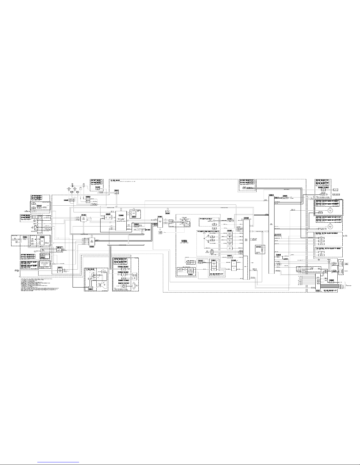
CCD-TRV3E/TRV13E/TRV23E/TRV45E/TRV55E/TRV65E/
TRV69E/TRV75/TRV75PK/TRV715
SECTION 3
BLOCK DIAGRAMS
3-1. OVERALL BLOCK DIAGRAM
3-1 3-2
3-3
3-4
Page 44
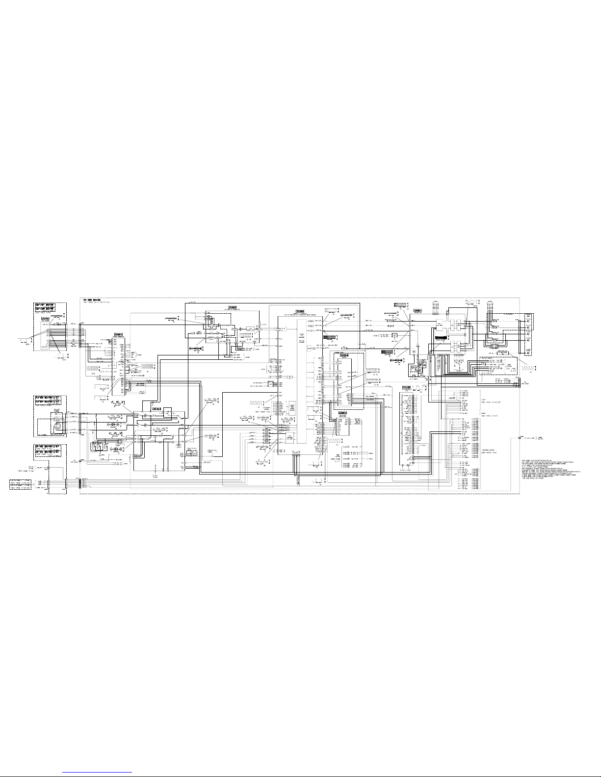
CCD-TRV3E/TRV13E/TRV23E/TRV45E/TRV55E/TRV65E/
TRV69E/TRV75/TRV75PK/TRV715
3-5
3-6 3-7
3-8
3-2. CAMERA/VIDEO 1 BLOCK DIAGRAM
H
7Vp-p
IC401
1 2
,
H
7Vp-p
IC401
3 4
H
1.3Vp-p
IC401
7
H
0.46Vp-p
IC151
3
H
0.32Vp-p
IC151
5
H
1.8Vp-p
IC151
60
H
1.4Vp-p
IC151
64
H
IC151 29 (
2.1Vp-p
)
H
1.4Vp-p
IC151
17
H
1.8Vp-p
IC151
25
H
IC151 62 (
1.6Vp-p
)
: 28.636 MHz
: 28.375 MHz
2.3Vp-p
IC501
CAMERA REC
5
NTSC
PAL
: 14.32 MHz
: 14.18 MHz
2.3Vp-p
IC501
CAMERA REC
11 12
NTSC
PAL
,
H
3Vp-p
IC501
44
CAMERA REC
3.2Vp-p
IC502
2 10
CAMERA REC
H
1.3Vp-p
IC502
26
CAMERA REC
H
0.4Vp-p
IC502
36
PB
—
0.14usec
V
3Vp-p
IC501
45
CAMERA REC
H
0.34Vp-p
IC202
3
CAMERA REC
H
0.84Vp-p
IC202
6
CAMERA REC
V
3Vp-p
IC202
81
CAMERA REC
3.2Vp-p
IC201
8
CAMERA REC
H
3Vp-p
IC202
80
PB
H
0.5Vp-p
IC202
13
CAMERA REC
H
0.4Vp-p
IC202
16
CAMERA REC
H
0.18Vp-p
IC202
23
CAMERA REC
H
0.18Vp-p
IC202
26
CAMERA REC
H
0.9Vp-p
IC202
33
CAMERA REC
V
0.4Vp-p
IC202
40
PB
IC202
66
3.58 MHz
3.1Vp-p
CAMERA REC
7.16 MHz
V
3Vp-p
IC201
19
CAMERA REC
H
3Vp-p
IC201
20
CAMERA REC
0.14usec
3.5Vp-p
IC204
12 15
CAMERA REC
—
3.5Vp-p
IC204
23 30
CAMERA REC
—
0.14usec
H
0.3Vp-p
IC001
3
CAMERA REC
2V
0.3Vp-p
IC001
TRIG : IC001
5 21
CAMERA REC
H
0.4Vp-p
IC001
7
PB
V
0.4Vp-p
IC001
11
PB
V
0.4Vp-p
IC001
17
PB
2V
2.9Vp-p
IC001
21
CAMERA REC
2V
3Vp-p
IC001
44 48
CAMERA REC
,
7Vp-p
Q001
C
CAMERA REC
4.12 MHz
Page 45
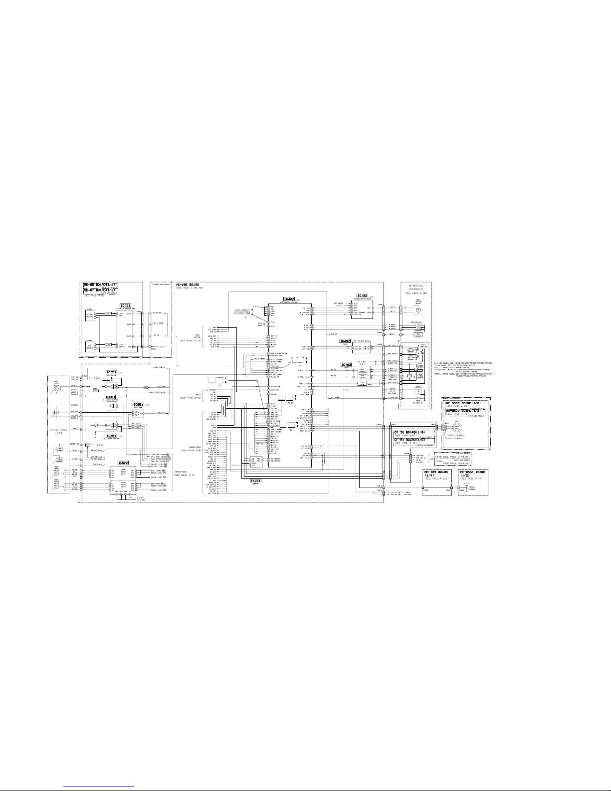
CCD-TRV3E/TRV13E/TRV23E/TRV45E/TRV55E/TRV65E/
TRV69E/TRV75/TRV75PK/TRV715
3-9
3-10
3-11
3-3. VTR/CAMEARA CONTROL BLOCK DIAGRAM
IC402
1
20 MHz
1.7Vp-p
4V
3Vp-p
IC402
48
2V
3Vp-p
IC402
55 57
,
2V
3Vp-p
IC402
47
13usec
3Vp-p
IC402
70
Page 46
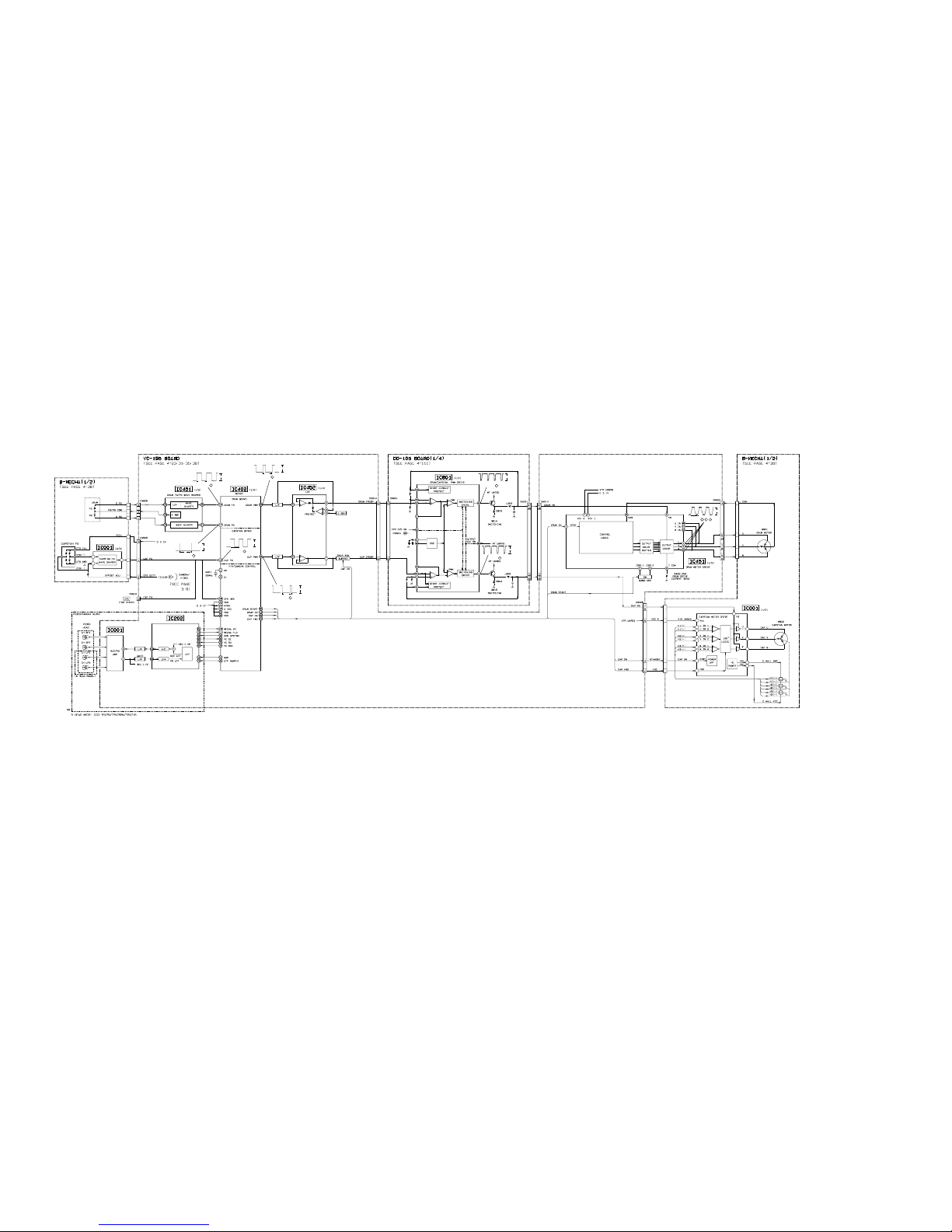
CCD-TRV3E/TRV13E/TRV23E/TRV45E/TRV55E/TRV65E/
TRV69E/TRV75/TRV75PK/TRV715
3-12
3-13 3-14
3-4. SERVO BLOCK DIAGRAM
3Vp-p
IC402
68
13usec
13usec
3Vp-p
IC402
69
1.2msec
3Vp-p
IC402
115
2.8msec
3Vp-p
IC402
116
2V
3Vp-p
IC402
117
5.6msec
1.2Vp-p
IC451 1 2 29,,
IC801 4
507 kHz
0.76Vp-p
IC801 64
506 kHz
0.76Vp-p
Page 47
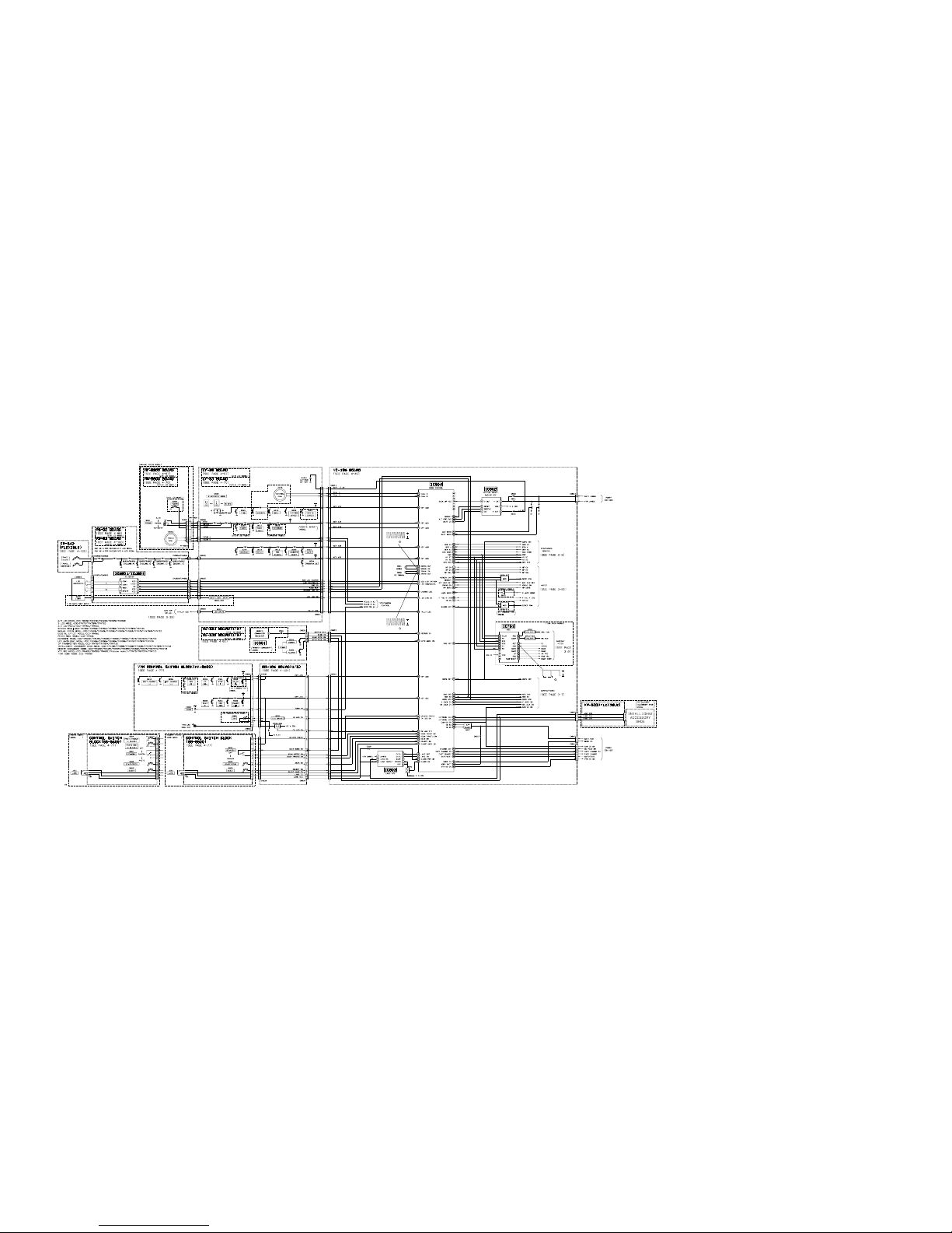
CCD-TRV3E/TRV13E/TRV23E/TRV45E/TRV55E/TRV65E/
TRV69E/TRV75/TRV75PK/TRV715
3-15 3-16
3-17
3-18
3-5. MODE CONTROL BLOCK DIAGRAM
CCD-TRV3E/TRV13E/TRV23E/TRV45E/TRV55E/TRV65E/
TRV69E/TRV75/TRV75PK/TRV715
IC604
41
20 MHz
1.5Vp-p
IC604
52
32 kHz
2.6Vp-p
H
3Vp-p
IC701
16
CAMERA REC
Page 48
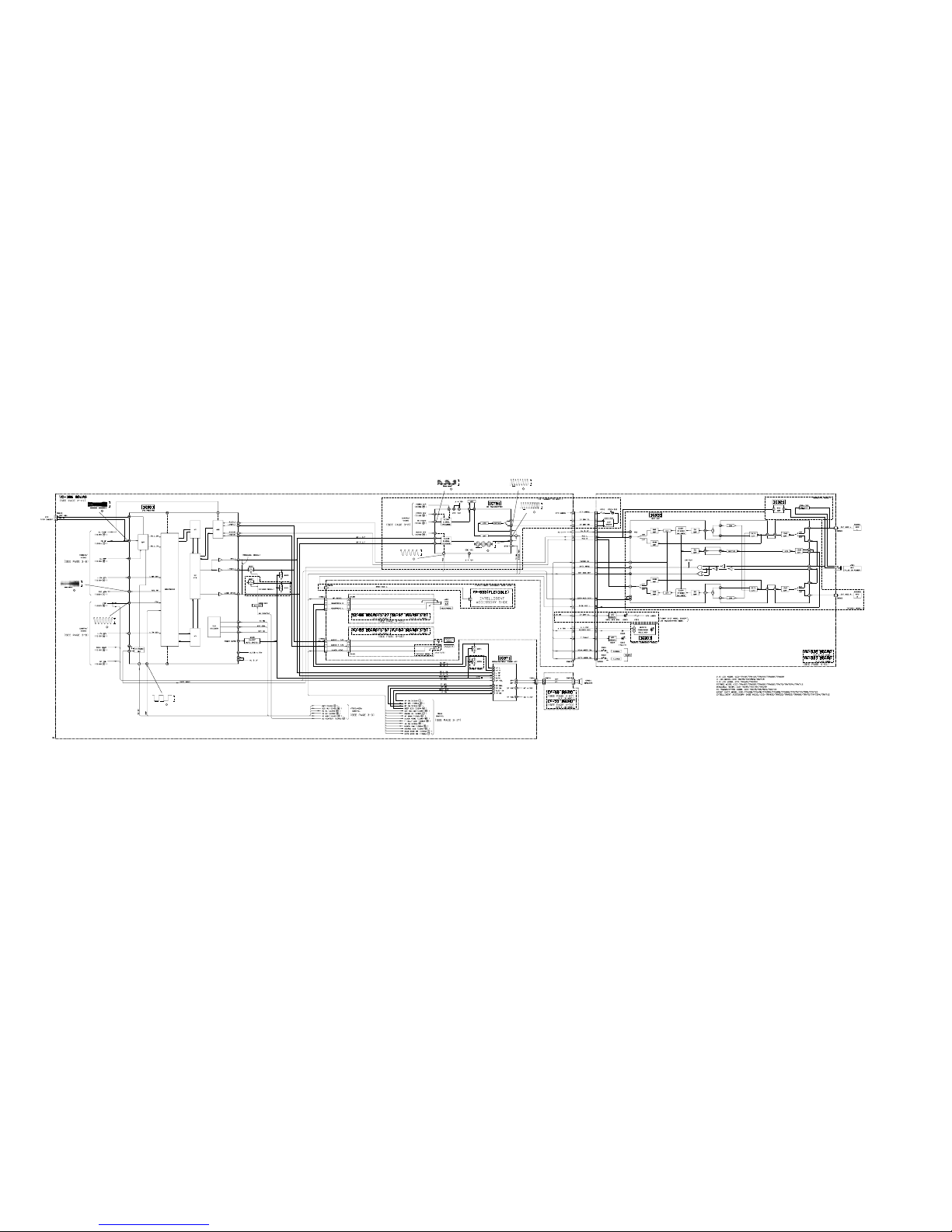
CCD-TRV3E/TRV13E/TRV23E/TRV45E/TRV55E/TRV65E/
TRV69E/TRV75/TRV75PK/TRV715
3-6. AUDIO BLOCK DIAGRAM
3-19
3-20 3-21
3-22
IC751
7
3.58 MHz
0.25Vp-p
2usec
0.5Vp-p
IC751
15
0.09usec
0.34Vp-p
IC751
16
0.09usec
0.7Vp-p
IC751
22
H
0.5Vp-p
IC751
41
2V
2.9Vp-p
IC301
21
CAMERA REC
V
0.4Vp-p
IC301
24
PB
V
0.36Vp-p
IC301
29
CAMERA REC
IC301
32
3.58 MHz
0.26Vp-p
CAMERA REC
Page 49
CCD-TRV3E/TRV13E/TRV23E/TRV45E/TRV55E/TRV65E/
TRV69E/TRV75/TRV75PK/TRV715
3-23
3-24
3-25
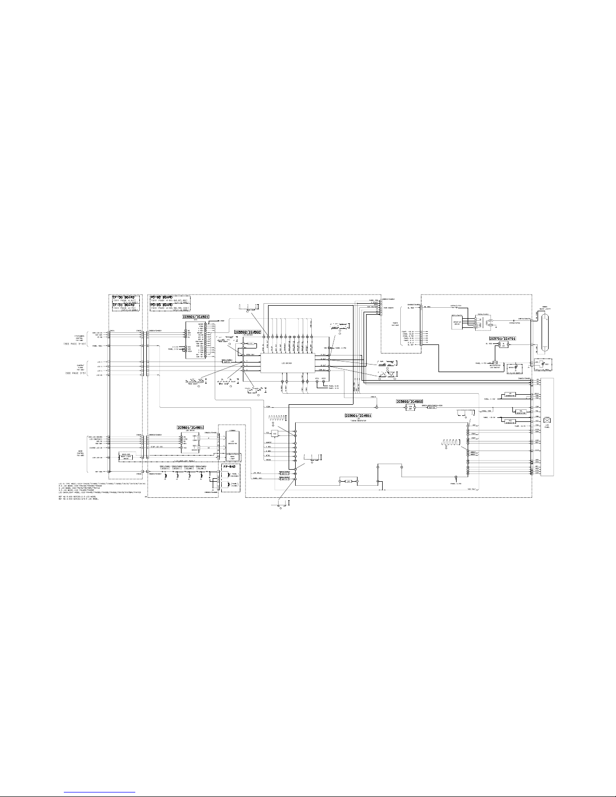
3-7. LCD (CCD-TRV23E/TRV45E/TRV55E/TRV65E/TRV69E/TRV75/TRV75PK/TRV715) BLOCK DIAGRAM
H
0.44Vp-p
IC4502/5502
8
H
0.2Vp-p
IC4502/5502
9
H
0.2Vp-p
IC4502/5502
10
H
0.7Vp-p
IC4502/5502
13
H
IC4502/5502
16
4.7Vp-p
H
IC4601/5601 4
4.7Vp-p
Approx. 3.7 MHz
IC4601 24
4.7Vp-p
20msec
IC4601/5601
34
4.7Vp-p
H
IC4601/560137
4.7Vp-p
IC4601 26
Approx.7.5MHz : 4.7Vp-p
IC5601 26
Approx.5.8MHz : 4.1Vp-p
2H
IC4502
20
2.2Vp-p
IC5502
20
4.2Vp-p
IC5502
22
2H
IC4502
22
2.3Vp-p
4.2Vp-p
2H
IC4502
24
2.3Vp-p
IC5502
24
4.2Vp-p
Approx.2.9 MHz
IC5601 24
4.7Vp-p
Page 50
CCD-TRV3E/TRV13E/TRV23E/TRV45E/TRV55E/TRV65E/
TRV69E/TRV75/TRV75PK/TRV715
3-26
3-27 3-28
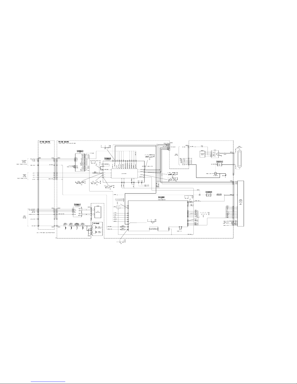
3-8. LCD (CCD-TRV3E/TRV13E) BLOCK DIAGRAM
H
0.44Vp-p
IC4502/5502
8
H
0.2Vp-p
IC4502/5502
9
H
0.2Vp-p
IC4502/5502
10
H
0.7Vp-p
IC4502/5502
13
H
IC4502/5502
16
3Vp-p
H
IC4601/5601 4
3Vp-p
20msec
IC4601/5601
34
3Vp-p
H
IC4601/560137
3Vp-p
IC4601 26
Approx. 9.5MHz : 3.3Vp-p
IC5601 26
Approx. 5.8MHz : 3.2Vp-p
2H
IC4502
20
3.3Vp-p
IC5502
20
3.6Vp-p
IC5502
22
2H
IC4502
22
3.3Vp-p
3.6Vp-p
2H
IC4502
24
3.3Vp-p
IC5502
24
3.6
Vp-p
24
Approx. 4.8 MHz
IC4601 24
3Vp-p
Approx. 2.9 MHz
IC5601
3.4Vp-p
Page 51
CCD-TRV3E/TRV13E/TRV23E/TRV45E/TRV55E/TRV65E/
TRV69E/TRV75/TRV75PK/TRV715
3-29 3-30
3-31
3-32
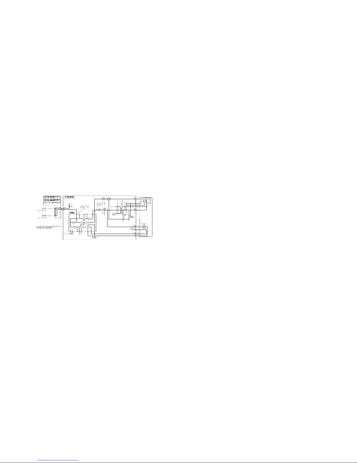
3-9. B/W EVF BLOCK DIAGRAM
CCD-TRV3E/TRV13E/TRV23E/TRV45E/TRV55E/TRV65E/
TRV69E/TRV75/TRV75PK/TRV715
H
1Vp-p
IC901
11
H
2.2Vp-p
IC901
13
Page 52
CCD-TRV3E/TRV13E/TRV23E/TRV45E/TRV55E/TRV65E/
TRV69E/TRV75/TRV75PK/TRV715
3-33
3-34 3-35
3-36 E
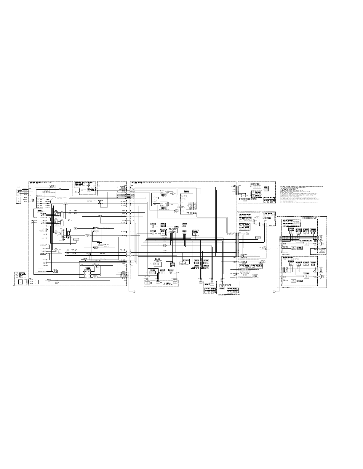
3-10. POWER BLOCK DIAGRAM
Page 53
CCD-TRV3E/TRV13E/TRV23E/TRV45E/TRV55E/TRV65E/
TRV69E/TRV75/TRV75PK/TRV715
4-1
4-2
4-3
SECTION 4
PRINTED WIRING BOARDS AND SCHEMATIC DIAGRAMS
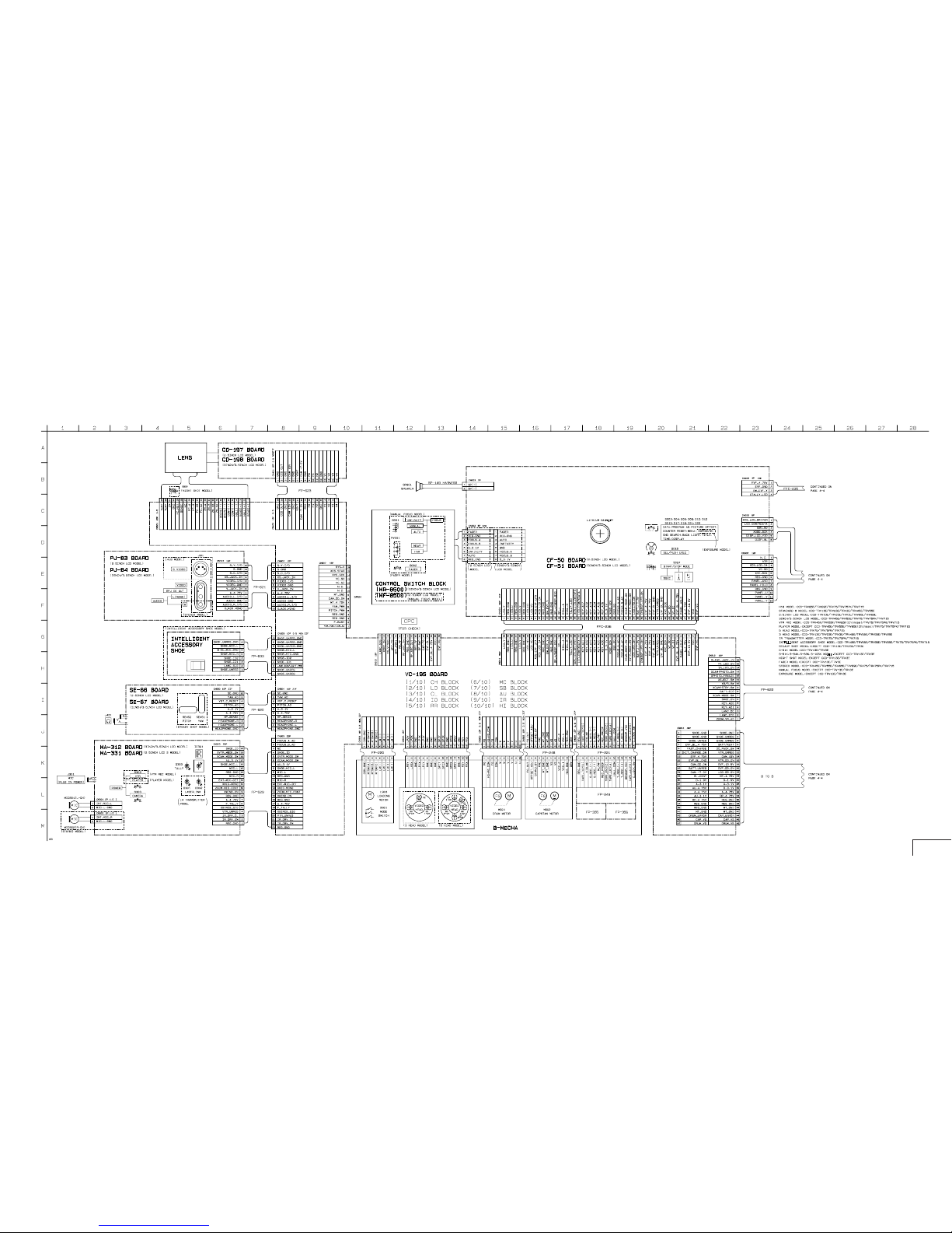
4-1. FRAME SCHEMATIC DIAGRAM (1)
FRAME
Page 54
CCD-TRV3E/TRV13E/TRV23E/TRV45E/TRV55E/TRV65E/
TRV69E/TRV75/TRV75PK/TRV715
4-4
4-5 4-6
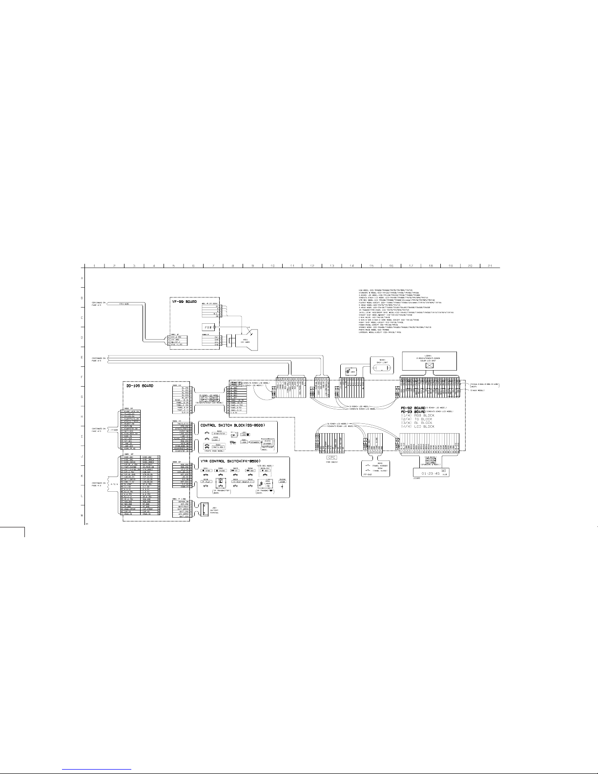
FRAME SCHEMATIC DIAGRAM (2)
FRAME
Page 55
CCD-TRV3E/TRV13E/TRV23E/TRV45E/TRV55E/TRV65E/
TRV69E/TRV75/TRV75PK/TRV715
• For printed wiring boards.
• b: Pattern from the side which enable seeing.
(The other layer's patterns are not indicated.)
• Circled numbers refer to waveforms.
• Through hole is omitted.
• There are few cases that the part printed on diagram isn’t
mounted in this model.
• Chip parts.
Transistor Diode
• For schematic diagrams.
• All capacitors are in µF unless otherwise noted. pF: µµF.
50 V or less are not indicated except for electrolytics and tantalums.
• Chip resistor are 1/16W unless otherwise noted.
kΩ : 1000Ω, MΩ : 1000kΩ.
• Caution when replacing chip parts.
New parts must be attached after removal of chip.
Be careful not to heat the minus side of tantalum capacitor, because
it is damaged by the heat.
• Some chip part will be indicated as follows.
Example C541 L452
22U 10UH
TA A 2520
• Constants of resistors, capasitors, ICs and etc with XX indicate
tha they are not used. In such cases, the unused circuits may be
indicated.
• Parts with differ according to the model/destination. Refer to
the mount table for each function.
• All variable and adjustable resistors have characteristic curve B,
unless otherwise noted.
• Signal name
XEDIT n EDIT PB/XREC n PB/REC
• 2 :non flammable resistor.
• 1 :fusible resistor.
• H :panel designation.
• A :B+ Line
• B :B– Line
• J : IN/OUT direction of (+, –) B LINE.
• C :adjustment for repair.
• Circled numbers refer to waveforms.
4-8 4-9
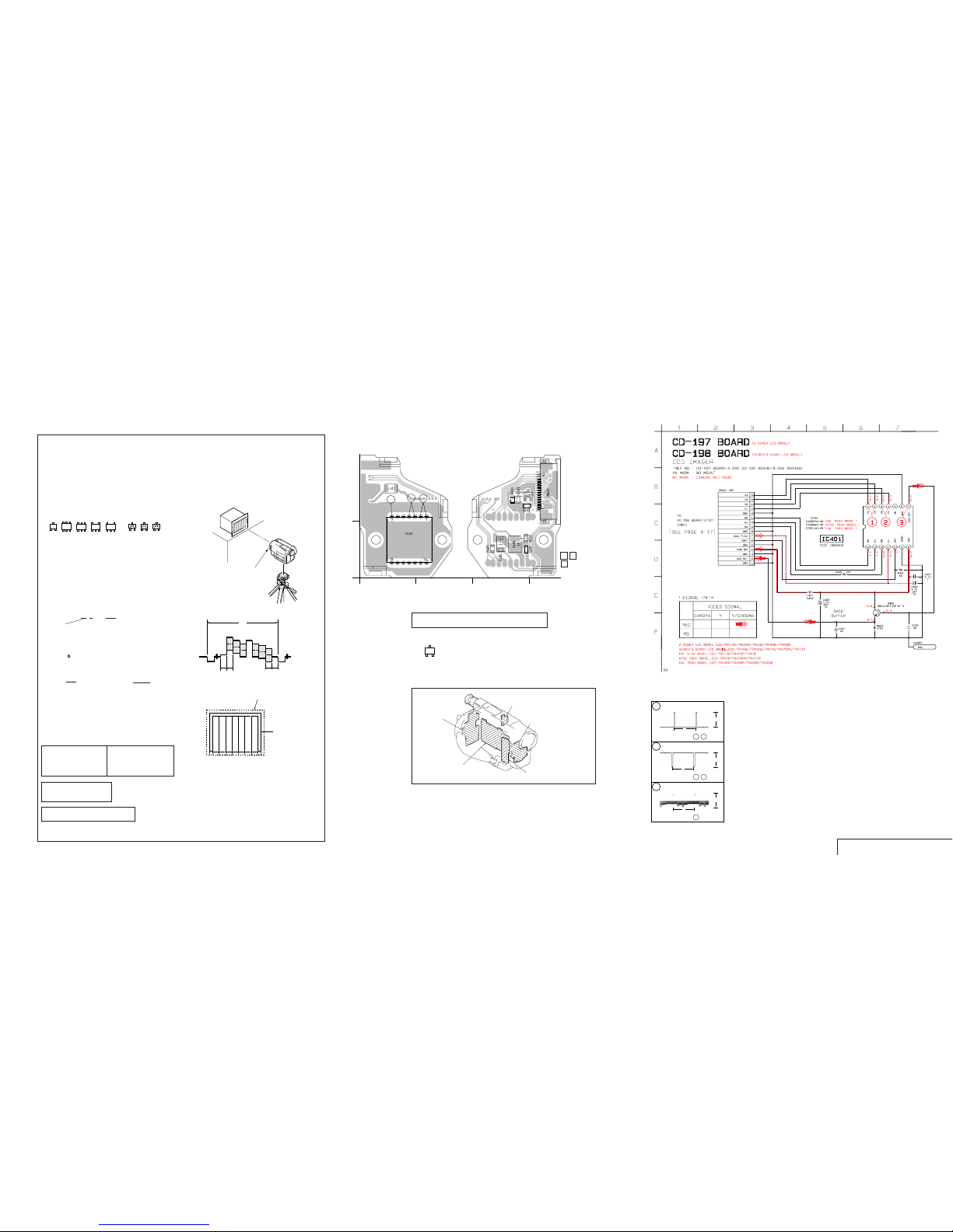
CD-197/198 (CCD IMAGER) (2.5 INCH LCD, 3 INCH/3.5 INCH LCD MODEL) PRINTED
WIRING BOARD
– Ref No. CD-197 BOARD: 4,000 series, CD-198 BOARD: 9,000 series –
CCD IMAGER
CD-197/198 (2.5INCH, 3 INCH/3.5 INCH LCD MODEL
Note on the CCD imager replacement
• The CCD imager is not mounted for the already mounted
CD-197/198 board supplied as the repair parts.
When replacing the CD-197/198 board, remove the CCD
imager from the old board and install on the new board.
• Perform all adjustments of the camera block when the CCD
imager has been replaced.
• Handle the CCD imager with attention such as MOS IC as it
may be broken by static electricity in the structure.
Also, prevent the receiving light section from dust attached
and strong light.
• For Printed Wiring Boards.
• Chip transistor
There are few cases that the part isn't mounted in this model is
printed on this diagram.
C
Q
BE
CD-197/
CD-198 BOARD
C401 A-3
C403 B-3
C405 A-3
C406 A-3
C407 B-3
CN401 B-4
IC401 A-1
L401 B-1
Q402 B-3
R401 A-3
R404 B-3
R405 A-3
4-2. PRINTED WIRING BOARDS AND SCHEMATIC DIAGRAMS
THIS NOTE IS COMMON FOR PRINTED WIRING BOARDS AND SCHEMATIC DIAGRAMS.
(In addition to this, the necessary note is printed in each block.)
• Measuring conditions voltage value and waveform.
• The object is color bar chart of pattern box.
• Voltages and dc between ground and measurement points.
Readings are taken with a digital multimeter (DC 10MΩ).
• Voltages variations may be noted due to normal production
tolerances.
1.Connection
2.Adjust the distance so that the output waveform of Fig. a and the
Fig. b can be obtain.
Fig. b (Picture on monitor TV)
Fig. a (Video output terminal output waveform)
Pattern box
1.5m
Kinds of capacitor
(
Â
External dimensions (mm)
Â
Temperature
chracteristics
Les composants identifiés par
une marque ! sont critiques
pour la sécurité.
Ne les remplacer que par une
piéce portant le numéro spécifié.
The components identified by
mark !or dotted line with mark
! are critical for safety.
Replace only with part number
specified.
When indicating parts by reference number, please include the
board name.
4-7
Lens reference plane
surface lmaging surface
of CCD imager
(IC401 on CD-197/198 board)
Electron beam
scanned frame
CRT picture frame
Yellow
Cyan
Green
White
Magenta
Red
Blue
A
B
B
A
A=B
H
Yellow
Cyan
Green
White
Magenta
Red
Blue
C
Q
BE
546
132
Q
564
312
Q
54
312
Q
21
Q
534
3
21
3213
21
CD-197/198 BOARD
CAMERA REC
H
7Vp-p
IC401
1 2
1
2
3
,
H
7Vp-p
IC401
3 4
H
1.3Vp-p
IC401
7
,
Refer to page 3 as for “Table for difference
of functions” of models and classification.
1234
A
B
09
CD-197/198 BOARD (SIDE B) CD-197/198 BOARD (SIDE A)
1-668-9451-668-936-
12
12 22
1
2
3
CD-197 (2.5 INCH LCD MODEL)
CD-198 (3 INCH/3.5 INCH LCD MODEL)
(CCD IMAGER)
PJ-83 (2.5 INCH LCD MODEL)
PJ-84 (3 INCH/3.5 INCH LCD MODEL)
(AV IN/OUT)
MA-331 (2.5 INCH LCD MODEL)
MA-312 (3 INCH/3.5 INCH LCD MODEL)
(STEREO MIC, LASER LINK)
CF-50 (2.5 INCH LCD MODEL)
CF-51 (3 INCH/3.5 INCH LCD MODEL)
(CONTROL)
DD-105
(POWER)
Page 56
CCD-TRV3E/TRV13E/TRV23E/TRV45E/TRV55E/TRV65E/
TRV69E/TRV75/TRV75PK/TRV715
4-10
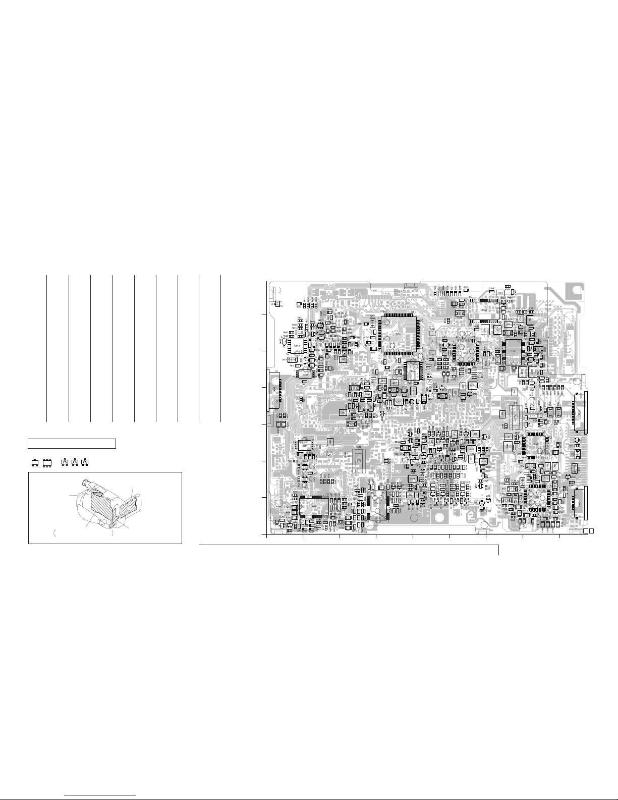
CAMERA, Y/C PROCESSOR, IN/OUT, REC/PB HEAD AMP, SERVO/SYSTEM CONTROL, SERVO, AUDIO, IR TRANSMITTER, MODE CONTROL
VC-195 (SIDE B)
4-12
4-11
VC-195 (CAMERA, Y/C PROCESSOR, IN/OUT, REC/PB HEAD AMP, SERVO/SYSTEM CONTROL, SERVO, AUDIO, IR TRANSMITTER, MODE CONTROL) PRINTED WIRING BOARD
– Ref No. VC-195 BOARD: 1,000 series –
C213 D-5
C217 D-4
C218 D-4
C227 D-5
C229 E-5
C232 D-3
C233 D-5
C234 D-5
C235 D-3
C236 D-3
C239 E-4
C241 E-3
C243 F-3
C244 F-3
C245 D-4
C246 D-4
C247 D-4
C249 E-4
C252 F-3
C301 B-9
C312 C-9
C371 E-8
C372 E-8
C378 F-7
C380 E-7
C381 E-7
C382 F-8
C383 E-8
C384 E-8
C385 E-8
C387 F-8
C388 E-8
C402 C-1
C413 B-2
C451 A-3
C452 A-3
C453 A-3
C454 A-3
C455 A-3
C456 A-4
C457 A-3
C458 A-4
C459 A-4
C460 A-4
C461 A-3
C462 A-4
C463 A-3
C464 B-3
C465 B-4
C466 B-3
C467 B-3
C468 B-3
C469 B-4
C470 B-4
C471 B-4
C473 A-1
C474 A-2
C475 A-2
C476 A-2
C477 A-2
C478 A-2
C479 A-2
C480 A-2
C481 A-1
C482 A-2
C483 A-2
C484 A-2
C485 A-1
C504 E-6
C505 E-6
C506 E-7
C507 E-6
C508 E-6
C509 E-7
C510 E-6
C514 E-5
C515 E-5
C518 F-5
C553 G-6
C554 G-7
C556 G-7
C557 G-5
C558 G-5
C559 F-7
C563 F-6
C564 F-7
C566 G-7
C569 G-6
C572 F-6
C603 F-1
C607 E-2
C610 F-2
C611 F-2
C613 E-1
C625 E-2
C626 E-2
C627 F-2
C630 F-3
C634 F-3
C636 F-2
C704 F-7
C714 F-8
C715 F-8
C751 B-6
C752 A-7
C753 A-7
C754 A-7
C755 A-7
C756 A-7
C757 A-7
C758 A-8
C759 B-6
C760 B-6
C761 B-8
C762 B-8
C763 B-8
C764 B-8
C765 A-8
C766 A-8
C767 B-8
C768 B-8
C769 A-8
C770 A-8
C771 B-8
C772 A-8
C773 B-8
C774 A-8
C775 A-8
C776 B-8
C777 A-8
C778 B-9
C781 B-8
CN904 A-9
CN907 D-9
CN910 D-1
D001 C-4
D201 D-3
D202 D-3
D371 E-8
D502 F-5
D601 E-2
D602 E-2
D604 F-2
D608 F-1
D609 F-2
D611 E-2
D910 G-1
FB202 E-4
FB203 E-4
FB204 F-3
FB205 F-3
FB206 D-4
FB501 E-5
FB502 E-6
FB503 E-5
FB504 E-5
FB505 E-5
FB506 E-5
IC152 C-8
IC201 E-5
IC204 F-4
IC371 E-7
IC401 C-2
IC403 B-2
IC404 B-2
IC451 A-4
IC452 A-2
IC501 E-6
IC552 G-6
IC602 E-2
IC751 A-8
L002 B-4
L003 B-4
L007 C-6
L008 C-6
L010 C-6
L011 C-6
L014 C-5
L015 C-5
L017 C-5
L019 B-6
L152 D-8
L153 D-7
L154 D-7
L156 C-7
L201 D-3
L202 D-4
L203 D-6
L204 D-4
L205 D-6
L206 D-3
L207 E-4
L209 E-4
L402 C-2
L501 E-6
L552 F-7
L553 G-7
L602 E-3
L701 F-7
L702 F-7
L704 F-8
L751 B-8
L752 B-8
L753 B-8
Q003 A-5
Q004 A-6
Q005 A-5
Q006 A-5
Q007 A-6
Q008 B-6
Q009 B-6
Q010 B-5
Q011 B-5
Q012 B-5
Q016 B-5
Q017 B-6
Q018 C-5
Q019 C-6
Q021 B-6
Q023 C-6
Q025 C-6
Q026 C-6
Q030 C-5
Q031 C-5
Q032 C-7
Q035 C-4
Q037 C-4
Q038 C-5
Q039 C-5
Q041 B-5
Q042 C-4
Q151 D-8
Q202 D-3
Q203 D-3
Q204 D-5
Q205 E-5
Q208 D-6
Q217 D-4
Q218 D-4
Q306 B-9
Q307 C-9
Q311 A-6
Q312 A-7
Q451 B-3
Q452 B-4
Q453 B-4
VC-195 BOARD
(SIDE B)
C002 A-5
C003 A-5
C008 A-4
C009 B-5
C011 B-5
C012 B-5
C013 B-6
C014 B-6
C015 B-5
C016 B-5
C017 B-5
C019 B-5
C020 B-6
C022 B-5
C025 B-6
C038 B-6
C040 B-6
C042 B-5
C043 B-5
C048 B-6
C050 C-6
C051 B-5
C054 B-5
C056 B-5
C058 B-6
C060 C-5
C066 B-6
C067 C-6
C068 C-6
C069 C-5
C070 C-6
C072 C-6
C074 C-6
C076 C-5
C077 C-5
C080 C-5
C083 C-5
C086 C-4
C087 C-4
C090 C-6
C152 D-8
C157 E-8
C158 D-8
C159 C-8
C174 D-8
C175 D-8
C176 D-8
C182 D-8
C183 D-8
C190 D-8
C191 C-7
C192 C-7
C202 D-3
C203 D-3
C204 D-4
C205 E-4
C206 D-4
C207 D-3
C208 D-3
C209 D-6
C210 D-6
C211 D-3
C212 D-3
Q454 A-1
Q455 A-1
Q551 G-7
Q607 F-2
Q619 E-3
Q620 F-2
Q705 F-7
R001 A-6
R002 A-6
R008 A-4
R009 A-5
R010 B-6
R011 B-5
R012 B-5
R013 B-6
R014 B-4
R015 B-5
R016 B-6
R017 B-6
R018 B-5
R019 B-5
R020 B-4
R021 B-5
R023 B-6
R025 B-6
R029 B-5
R031 B-5
R040 B-5
R041 B-5
R042 B-5
R047 B-5
R048 B-5
R049 B-6
R050 B-6
R051 B-6
R056 B-6
R058 B-6
R066 B-6
R067 C-6
R068 C-7
R069 C-5
R069 C-6
R070 C-6
R076 C-6
R077 C-6
R078 C-6
R079 C-6
R080 C-6
R083 C-5
R084 C-5
R087 C-5
R088 C-5
R090 C-5
R094 C-5
R095 C-7
R097 C-5
R100 C-5
R104 C-5
R105 C-6
R106 C-6
R109 B-4
R110 B-5
• For Printed Wiring Boards.
• This board is four-layer print board. However, the patterns of
layers 2 to 3 have not been included in the diagram.
• Chip transistor Chip diode
There are few cases that the part isn't mounted in this model is
printed on this diagram.
3213213
21
R112 C-7
R152 D-8
R154 D-8
R157 D-8
R179 D-8
R180 D-8
R183 E-8
R184 E-8
R202 D-3
R203 D-4
R204 D-3
R205 D-3
R206 D-4
R208 D-3
R210 D-3
R211 D-3
R212 D-6
R214 D-5
R215 D-5
R216 D-5
R217 E-4
R223 D-3
R224 D-3
R226 D-4
R240 D-4
R244 D-3
R246 D-3
R247 D-3
R248 E-3
R249 E-3
R250 F-3
R254 D-1
R255 E-5
R257 D-4
R304 B-9
R305 C-9
R329 A-6
R330 A-7
R371 D-8
R372 D-8
R373 D-9
R374 D-8
R375 D-8
R376 D-8
R377 E-8
R378 E-8
R379 E-7
R382 E-8
R383 E-8
R384 E-7
R385 F-8
R386 F-8
R386 F-8
R388 E-8
R389 E-8
R403 C-2
R404 C-3
R415 B-2
R416 B-2
R417 B-2
R418 B-2
R426 C-2
R427 B-2
R428 B-2
R429 B-1
R430 B-1
R432 C-2
R433 C-2
R434 C-2
R452 A-3
R453 A-3
R454 A-3
R455 A-3
R456 A-3
R457 A-3
R459 A-3
R460 A-3
R461 A-3
R462 A-3
R463 A-3
R467 A-2
R468 A-2
R469 A-2
R470 A-2
R471 A-2
R472 A-3
R473 A-1
R475 A-1
R477 A-2
R479 A-2
R480 A-2
R481 A-2
R482 A-2
R483 A-1
R484 A-1
R485 A-1
R486 B-1
R487 A-1
R504 E-6
R505 E-6
R508 E-5
R510 E-5
R511 E-5
R512 F-5
R527 E-5
R552 G-6
R555 G-7
R563 G-5
R564 G-6
R566 G-5
R567 G-6
R570 F-5
R579 G-6
R582 G-6
R603 F-2
R604 F-2
R608 F-2
R612 E-1
R618 F-1
R619 F-1
R620 F-1
R621 F-1
R622 F-2
R624 F-1
R625 F-2
R627 E-2
R628 E-2
R629 F-1
R630 F-2
R631 G-2
R632 G-1
R633 E-2
R634 E-2
R635 E-2
R636 E-2
R637 G-2
R638 G-2
R639 G-2
R640 F-2
R641 F-3
R642 F-2
R643 F-2
R644 F-2
R645 E-2
R646 F-2
R647 F-2
R648 F-2
R649 F-2
R651 F-2
R652 F-3
R653 F-3
R654 F-3
R655 F-2
R662 E-3
R663 F-3
R665 F-3
R678 F-3
R686 E-2
R687 E-2
R689 F-3
R690 F-2
R691 E-2
R692 F-1
R704 G-8
R705 G-7
R716 G-8
R717 F-8
R718 F-7
R719 F-8
R723 F-7
R752 A-7
R753 A-7
R754 B-6
R755 B-6
R757 A-7
R758 A-7
R759 A-7
R760 B-8
R761 A-8
R762 A-8
R763 A-8
R764 B-8
R765 B-8
R766 A-8
R767 B-8
R768 A-8
R770 A-8
R771 A-8
R772 A-8
R773 B-8
R774 B-9
R775 A-8
R921 B-1
R922 D-1
R923 D-1
R924 D-1
R925 D-1
R926 G-7
R927 G-7
RB12 C-8
RB151 D-8
TH401 B-4
X151 D-7
X401 B-3
X501 F-5
C
Q
BE
546
132
Q
123456789
A
B
C
D
E
F
G
09
VC-195 BOARD (SIDE B)
1-668-928-
11 21
63
64
65
66
67
56
5758
28
29
25
26
27
1
2 3
4
5
6
CCD-TRV3E/TRV13E/TRV23E/TRV45E/TRV55E/TRV65E/
TRV69E/TRV75/TRV75PK/TRV715
VC-195
CAMERA, Y/C PROCESSOR, IN/OUT,
REC/PB HEAD AMP, SERVO/SYSTEM CONTROL,
SERVO, AUDIO, IR TRANSMITTER, MODE CONTROL
VF-99
(B/W EVF)
SE-66 (2.5 INCH LCD MODEL)
SE-67 (3 INCH/3.5 INCH LCD MODEL)
(STEADY SHOT)
PD-92 (2.5 INCH LCD MODEL)
PD-93 (3 INCH/3.5 INCH LCD MODEL)
(RGB DECODER, LCD, LCD DRIVE, BACK LIGHT)
Page 57
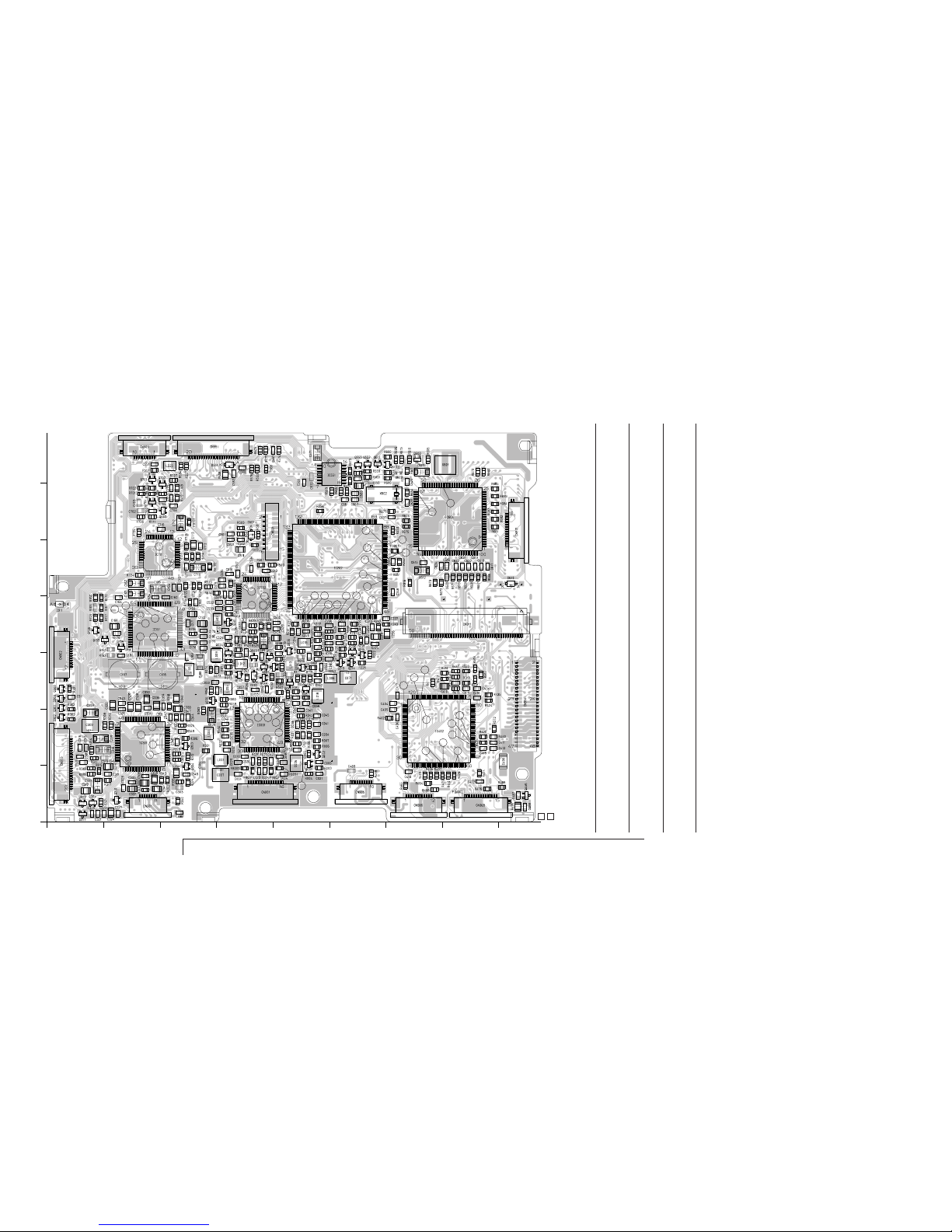
CCD-TRV3E/TRV13E/TRV23E/TRV45E/TRV55E/TRV65E/
TRV69E/TRV75/TRV75PK/TRV715
4-15
CAMERA, Y/C PROCESSOR, IN/OUT, REC/PB HEAD AMP, SERVO/SYSTEM CONTROL, SERVO, AUDIO, IR TRANSMITTER, MODE CONTROL
VC-195 (SIDE A)
4-144-13
VC-195 BOARD
(SIDE A)
C001 A-13
C004 A-14
C004 B-13
C005 B-14
C006 B-14
C007 A-13
C010 B-13
C018 B-14
C021 A-14
C023 A-13
C024 A-13
C026 B-13
C027 B-13
C028 B-12
C029 B-13
C030 B-14
C031 B-13
C032 B-13
C033 B-14
C034 B-14
C035 C-14
C036 B-13
C037 B-14
C039 B-14
C041 B-14
C045 B-14
C046 C-14
C047 B-14
C049 C-14
C052 C-13
C053 C-14
C055 C-13
C057 C-13
C059 C-12
C061 C-13
C062 C-14
C065 C-14
C071 C-15
C073 C-13
C075 C-13
C078 C-14
C079 C-13
C081 C-14
C082 C-14
C084 D-14
C085 C-14
C088 C-14
C089 C-13
C156 E-12
C160 D-12
C161 E-12
C162 E-11
C163 E-11
C164 D-11
C166 D-12
C168 D-11
C169 D-12
C170 D-11
C171 D-12
C172 D-12
C173 D-12
C177 D-12
C178 D-12
C179 D-12
C180 D-12
C181 C-11
C184 D-11
C185 C-12
C186 E-11
C187 C-11
C188 C-12
C189 C-12
C201 E-16
C214 D-14
C215 D-15
C219 D-15
C220 D-14
C221 D-14
C222 D-14
C223 D-15
C224 D-15
C225 D-15
C226 D-16
C228 D-15
C230 D-14
C237 D-16
C245 D-15
C248 E-16
C250 D-15
C303 A-12
C304 A-12
C306 B-10
C307 A10
C308 B-10
C309 B-10
C310 B-10
C311 C-10
C312 A10
C313 B-10
C314 A-11
C315 B-10
C316 B-10
C317 A-11
C318 B-10
C319 B-11
C320 A10
C321 A10
C322 C-11
C323 A-11
C324 A-11
C324 A-12
C325 C-11
C326 C-11
C327 A-11
C328 C-11
C330 C-11
C331 C-11
C332 A-11
C333 A-11
C334 C-12
C335 A-11
C336 C-11
C337 A-11
C338 B-12
C339 A-11
C340 C-12
C341 A-11
C342 B-12
C343 C-11
C344 B-12
C345 A-12
C346 B-12
C347 B-12
C348 A-12
C349 B-12
C404 C-16
C405 B-16
C406 B-16
C410 C-17
C411 B-17
C412 B-17
C414 C-17
C415 C-17
C416 C-17
C417 C-16
C418 A-16
C419 B-17
C420 C-17
C472 A-17
C486 A-12
C487 A-18
C488 A-18
C489 A-15
C490 B-18
C501 F-13
C502 E-13
C503 E-13
C511 E-13
C512 D-13
C513 E-13
C516 E-13
C517 E-13
C519 E-13
C520 E-13
C521 E-13
C522 D-13
C523 D-13
C524 D-13
C525 D-13
C526 D-13
C527 D-13
C528 D-14
C529 D-14
C530 D-14
C531 D-13
C532 D-13
C533 D-13
C534 E-13
C535 E-13
C551 G-11
C552 G-13
C555 G-15
C560 F-14
C561 F-15
C562 F-15
C565 F-15
C567 G-14
C568 G-13
C570 G-14
C571 G-14
C604 F-17
C605 G-16
C612 E-16
C615 E-16
C616 E-17
C617 E-17
C618 E-17
C619 E-17
C620 E-17
C621 E-17
C622 E-17
C623 E-17
C624 E-16
C628 F-16
C629 F-16
C637 F-16
C702 F-11
C703 F-11
C705 F-12
C706 F-12
C707 F-12
C708 F-12
C709 F-11
C710 E-12
C711 E-12
C712 E-12
C713 E-12
C716 F-12
C717 F-12
CN001 A-13
CN501 F-14
CN551 G-12
CN901 A-11
CN902 C-10
CN903 B-10
CN905 A-15
CN906 A-16
CN908 A-17
CN909 G-11
CN911 D-17
CN912 F-18
CN914 B-18
D002 C-13
D501 F-13
D551 G-13
D610 E-18
D911 D-10
FB001 A-13
FB002 A-13
FB003 A-13
FB004 A-14
FB201 E-16
FB701 F-12
FB702 E-12
IC001 B-13
IC151 D-11
IC202 E-15
IC301 B-11
IC402 B-16
IC502 D-13
IC551 G-15
IC701 E-11
L001 B-13
L004 B-12
L005 C-13
L006 C-15
L009 C-13
L012 C-13
L013 C-14
L016 D-14
L018 C-14
L155 C-12
L502 D-13
L555 G-12
Q001 B-14
Q002 B-14
Q020 C-12
Q022 C-14
Q024 C-13
Q027 C-13
Q028 C-13
Q029 C-13
Q033 C-14
Q034 C-14
Q036 D-14
Q040 C-14
Q043 C-13
Q044 C-13
Q153 D-11
Q154 D-11
Q156 D-10
Q213 C-15
Q214 C-15
Q215 C-15
Q216 C-15
Q301 C-10
Q302 B-10
Q303 B-12
Q304 A-12
Q305 A10
Q308 C-10
Q309 C-10
Q310 A-11
Q329 A-11
Q371 A10
Q372 A10
Q456 A-18
Q501 D-13
Q553 G-15
Q608 G-16
Q609 G-16
Q610 G-16
Q611 G-15
Q701 G-11
Q702 F-12
Q703 F-12
Q704 F-11
R003 A-14
R004 A-14
R005 B-14
R006 B-14
R007 B-14
R026 B-13
R027 B-13
R032 B-13
R033 B-14
R034 B-13
R035 B-14
R037 B-14
R038 B-14
R039 B-14
R043 C-13
R045 B-14
R046 C-14
R052 C-14
R055 C-14
R057 C-14
R059 C-13
R060 C-13
R062 B-12
R063 C-14
R064 C-14
R065 C-14
R072 C-13
R073 C-13
R074 C-12
R075 C-13
R081 D-13
R082 D-13
R085 C-13
R092 C-14
R093 C-13
R096 C-14
R098 D-14
R099 C-14
R101 D-14
R102 C-14
R103 C-14
R107 C-14
R113 C-14
R161 D-11
R162 C-11
R165 D-10
R166 D-10
R167 D-10
R170 D-10
R175 D-12
R176 D-12
R177 D-10
R178 D-10
R218 D-14
R219 D-15
R220 D-15
R222 C-15
R225 C-15
R227 D-14
R228 D-14
R229 D-14
R230 D-15
R231 D-15
R232 C-15
R233 D-14
R234 D-15
R236 D-14
R237 D-14
R238 D-15
R239 D-15
R241 D-14
R242 D-15
R243 D-16
R251 E-16
R252 E-16
R253 F-16
R256 F-14
R302 C-10
R303 B-10
R306 B-12
R308 B-11
R309 B-12
R310 B-11
R311 B-10
R312 B-12
R313 A10
R314 B-10
R315 A10
R316 A10
R317 A-11
R318 C-12
R319 A-11
R321 A10
R322 A-12
R323 B-12
R325 B-12
R326 A-12
R327 C-1
R328 B-12
R331 B-12
R343 A-12
R350 A-12
R402 B-16
R405 A-16
R406 A-16
R407 A-16
R409 A-16
R410 A-17
R411 C-16
R412 C-17
R413 C-17
R414 C-17
R419 C-17
R420 B-17
R421 B-17
R424 C-17
R425 A-17
R431 C-17
R435 C-17
R440 B-17
R441 C-17
R458 A-15
R464 A-16
R465 A-16
R466 A-16
R474 A-17
R476 A-17
R488 A-18
R490 A-18
R501 F-13
R502 F-13
R503 F-13
R507 E-13
R509 E-13
R513 D-13
R514 E-13
R521 D-13
R522 D-13
R523 D-13
R524 D-13
R525 D-13
R526 D-13
R527 B-17
R529 E-12
R551 G-11
R552 G-15
R553 G-13
R554 G-12
R556 G-13
R557 G-12
R558 F-15
R559 G-15
R560 G-15
R561 G-15
R562 G-15
R565 F-15
R568 G-13
R569 F-15
R571 F-15
R573 G-15
R574 G-14
R575 G-13
R576 G-13
R577 G-13
R605 G-16
R606 G-16
R610 G-16
R611 G-16
R613 G-16
R614 G-16
R650 F-16
R666 E-17
R667 E-17
R668 E-17
R669 E-17
R670 E-17
R671 E-17
R672 E-16
R673 E-16
R675 F-16
R676 F-16
R679 G-17
R680 G-17
R681 F-17
R682 F-17
R683 F-17
R684 F-17
R685 F-17
R693 F-17
R695 G-16
R696 G-16
R701 F-11
R702 F-11
R703 F-11
R706 F-11
R707 G-12
R708 F-12
R709 F-12
R710 F-12
R711 F-11
R712 E-12
R713 E-12
R714 E-12
R715 E-12
R720 E-12
R721 E-12
R722 E-12
R724 E-11
R725 F-11
R726 F-11
R916 E-16
R917 C-17
R918 C-17
R919 C-17
R920 C-17
X601 G-17
X602 F-15
47
34
59
62
60
61
30
31
32
33
32
34
33
44
9
7
8
35
36
37
38
39
40
41
43
42
10 11
12 13
14
15
16
17
24
23
22
21
20
19
18
68
69
46
49
48
50
51
52
55
54
53
45
10 11 12 13 14 15 16 17 18
A
B
C
D
E
F
G
09
VC-195 BOARD (SIDE A)
1-668-928-
11 21
CCD-TRV3E/TRV13E/TRV23E/TRV45E/TRV55E/TRV65E/
TRV69E/TRV75/TRV75PK/TRV715
Page 58
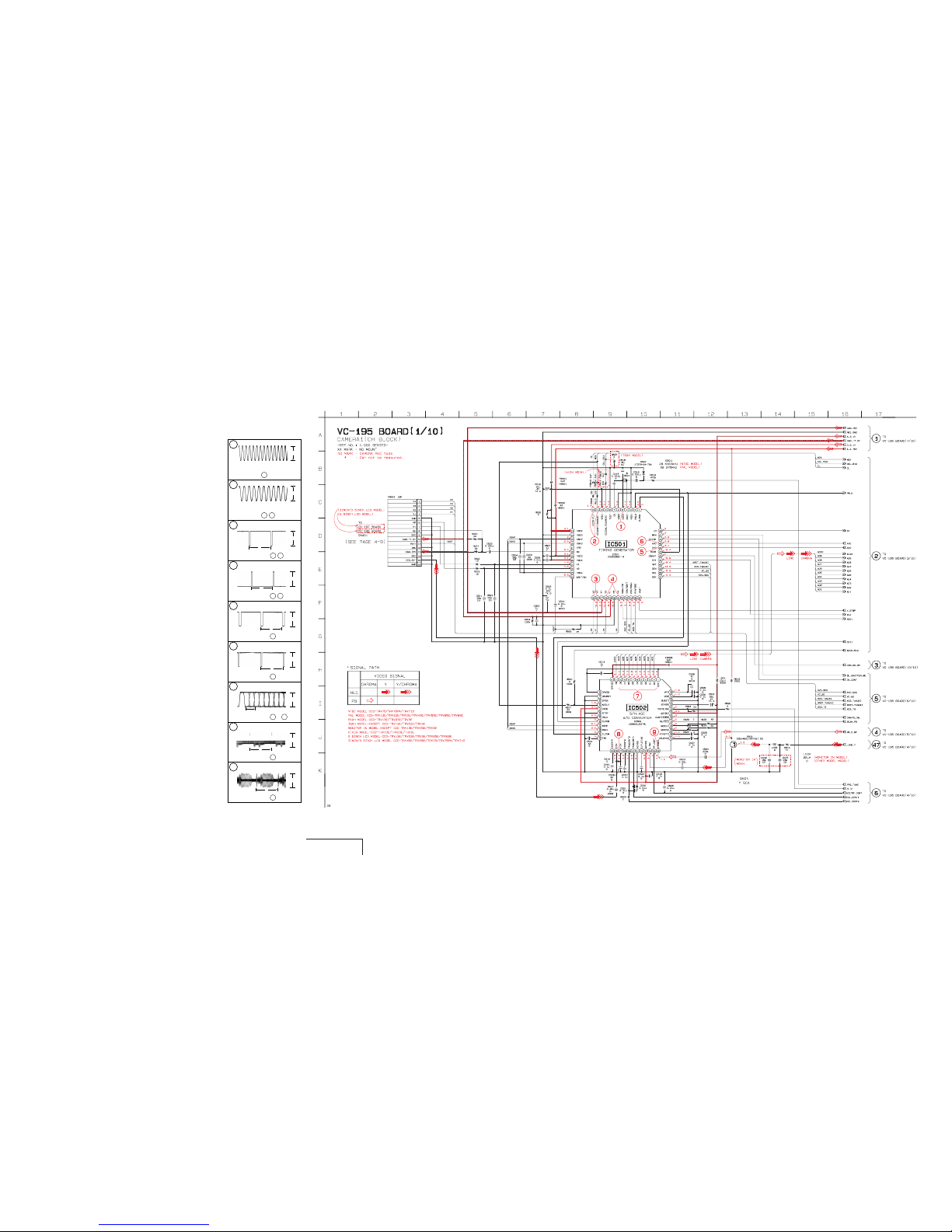
CCD-TRV3E/TRV13E/TRV23E/TRV45E/TRV55E/TRV65E/
TRV69E/TRV75/TRV75PK/TRV715
4-16
4-17
4-18
VC-195 BOARD (1/10)
1
2
3
4
5
6
7
8
9
: 28.636 MHz
: 28.375 MHz
2.3Vp-p
IC501
CAMERA REC
5
NTSC
PAL
: 14.32 MHz
: 14.18 MHz
2.3Vp-p
IC501
CAMERA REC
11 12
NTSC
PAL
,
H
7Vp-p
IC501
25
CAMERA REC
26
,
H
7Vp-p
IC501
28
CAMERA REC
31
,
H
3Vp-p
IC501
44
CAMERA REC
V
3Vp-p
IC501
45
CAMERA REC
3.2Vp-p
IC502
2 10
CAMERA REC
H
1.3Vp-p
IC502
26
CAMERA REC
H
0.4Vp-p
IC502
36
PB
—
0.14usec
CAMERA (1)
VC-195 (1/10)
CCD-TRV3E/TRV13E/TRV23E/TRV45E/TRV55E/TRV65E/
TRV69E/TRV75/TRV75PK/TRV715
Page 59
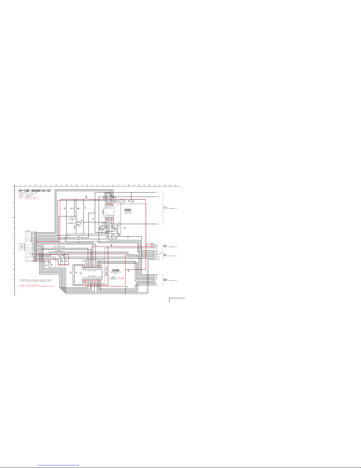
CCD-TRV3E/TRV13E/TRV23E/TRV45E/TRV55E/TRV65E/
TRV69E/TRV75/TRV75PK/TRV715
4-19 4-20
4-21
4-22
CAMERA (2)
VC-195 (2/10)
• For schematic diagrams.
• Refer to page 4–11 for Printed Wiring Board.
CCD-TRV3E/TRV13E/TRV23E/TRV45E/TRV55E/TRV65E/
TRV69E/TRV75/TRV75PK/TRV715
Page 60
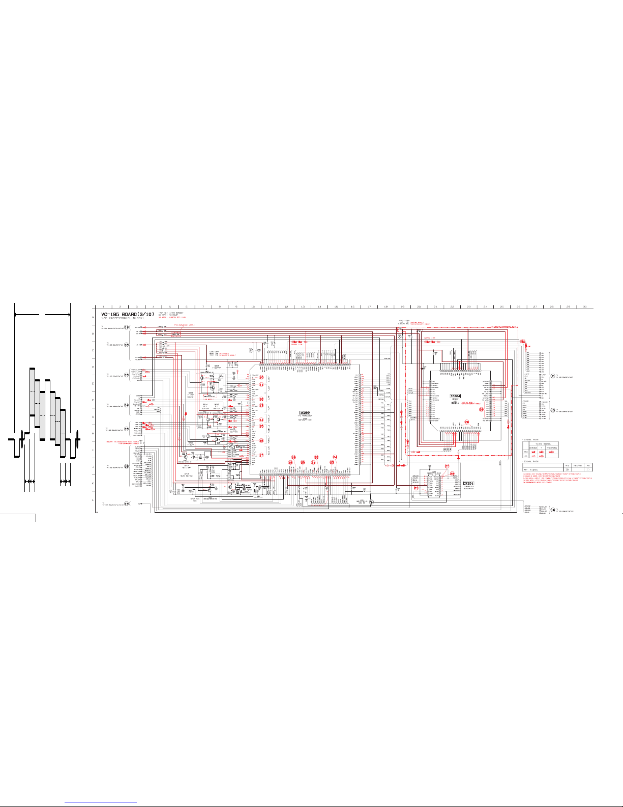
CCD-TRV3E/TRV13E/TRV23E/TRV45E/TRV55E/TRV65E/
TRV69E/TRV75/TRV75PK/TRV715
4-23
Y/C PROCESSOR
VC-195 (3/10)
A
B
B
A
A=B
H
Yellow
Cyan
Green
White
Magenta
Red
Blue
• For schematic diagrams.
• Refer to page 4–11 for Printed Wiring Board.
4-24 4-25 4-26
Page 61
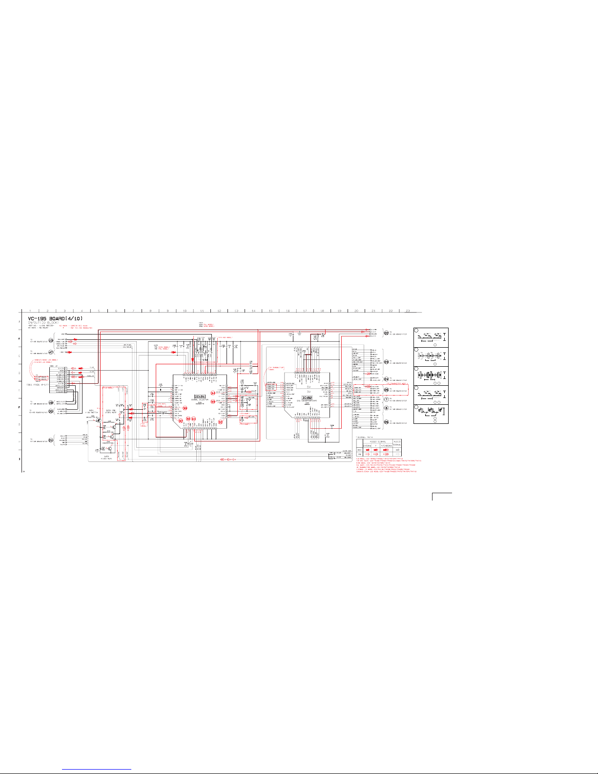
CCD-TRV3E/TRV13E/TRV23E/TRV45E/TRV55E/TRV65E/
TRV69E/TRV75/TRV75PK/TRV715
4-27 4-28
4-29 4-30
IN/OUT
VC-195 (4/10)
• For schematic diagrams.
• Refer to page 4–11 for Printed Wiring Board.
CCD-TRV3E/TRV13E/TRV23E/TRV45E/TRV55E/TRV65E/
TRV69E/TRV75/TRV75PK/TRV715
VC-195 BOARD (4/10)
CAMERA REC
H
0.46Vp-p
IC151
3
H
0.32Vp-p
IC151
5
30
31
32
33
34
H
IC151 29
IC151 62
(
2.1Vp-p
)
(
1.6Vp-p
)
H
1.4Vp-p
IC151
17 64
,
H
1.8Vp-p
IC151
25 60
,
Page 62
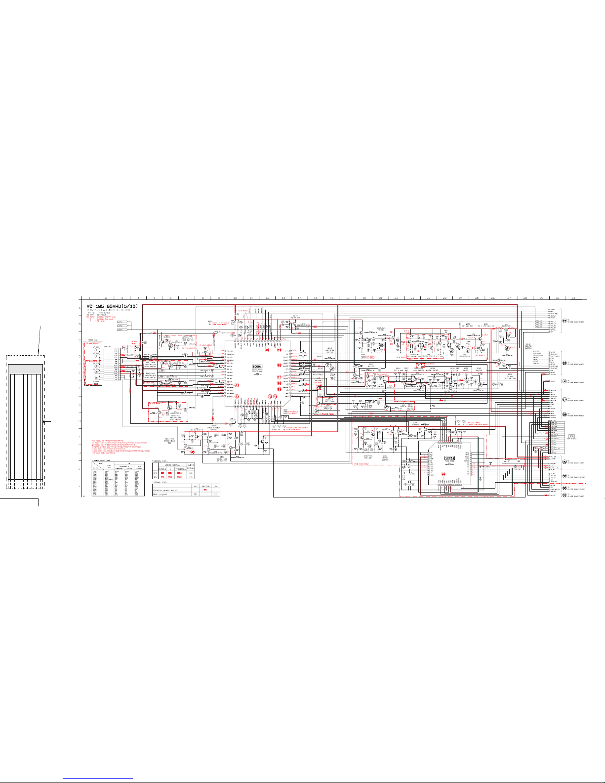
CCD-TRV3E/TRV13E/TRV23E/TRV45E/TRV55E/TRV65E/
TRV69E/TRV75/TRV75PK/TRV715
Electron beam
scanned frame
CRT picture frame
Yellow
Cyan
Green
White
Magenta
Red
Blue
4-31
REC/PB HEAD AMP
VC-195 (5/10)
4-32 4-33 4-34
• For schematic diagrams.
• Refer to page 4–11 for Printed Wiring Board.
Page 63
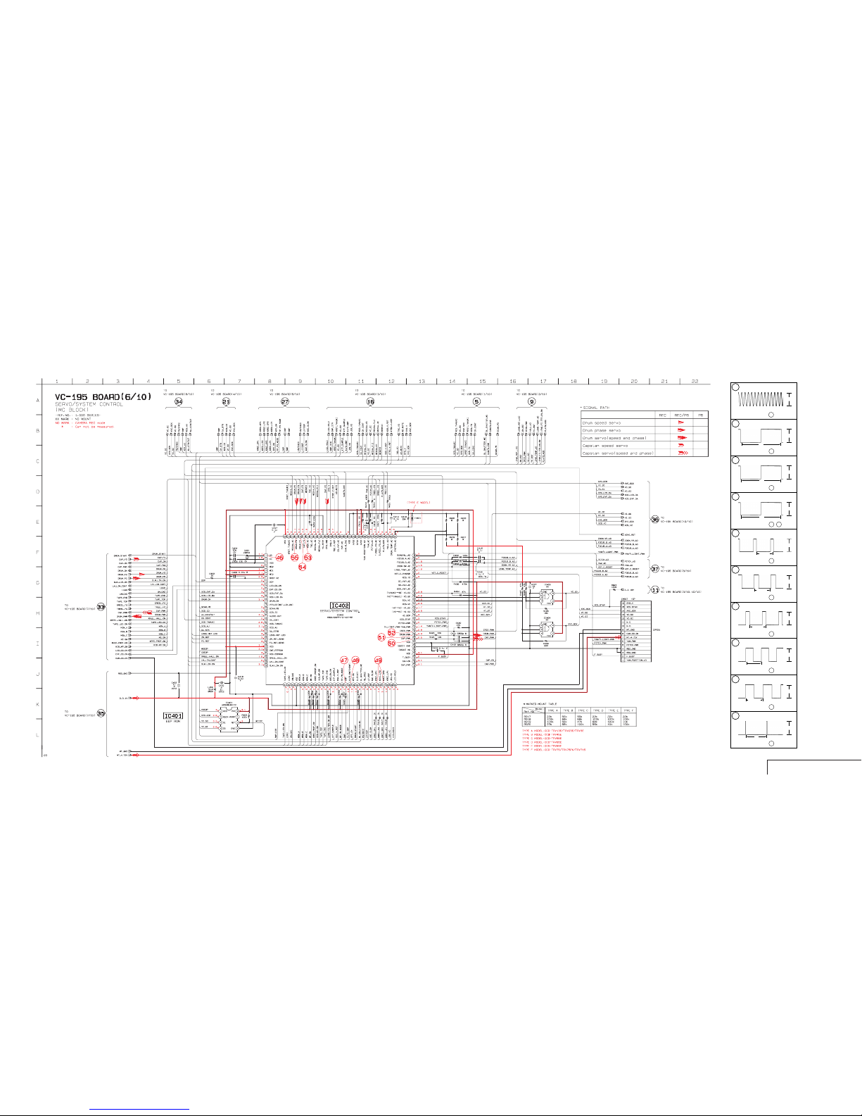
CCD-TRV3E/TRV13E/TRV23E/TRV45E/TRV55E/TRV65E/
TRV69E/TRV75/TRV75PK/TRV715
4-37
• For schematic diagrams.
• Refer to page 4–11 for Printed Wiring Board.
VC-195 BOARD (6/10)
CAMERA REC
2V
3Vp-p
IC402
47
4V
3Vp-p
IC402
48
2V
3Vp-p
IC402
55 57
3Vp-p
IC402
68
13usec
3Vp-p
IC402
69
13usec
3Vp-p
IC402
70
46
47
48
49
50
51
52
53
54
55
IC402
1
20 MHz
1.7Vp-p
1.2msec
3Vp-p
IC402
115
2.8msec
3Vp-p
IC402
116
2V
3Vp-p
IC402
117
,
13usec
SERVO/SYSTEM CONTROL
VC-195 (6/10)
4-35
4-36
Page 64
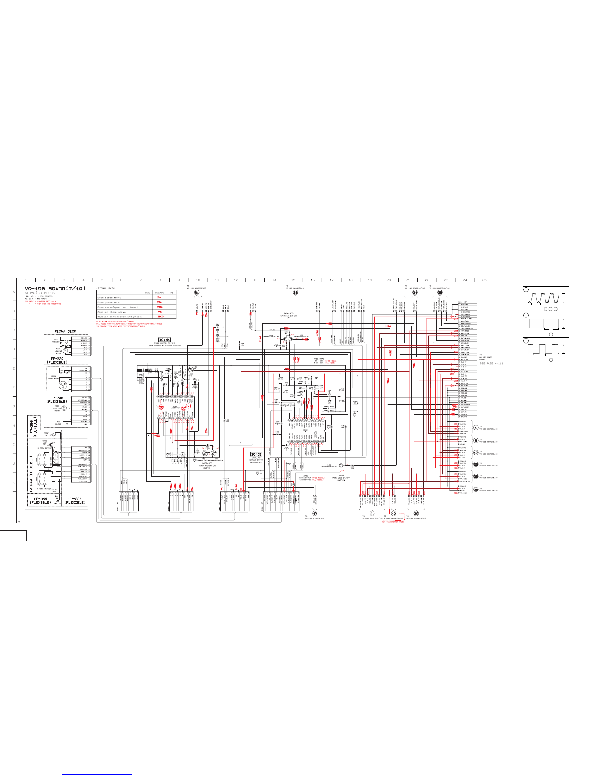
CCD-TRV3E/TRV13E/TRV23E/TRV45E/TRV55E/TRV65E/
TRV69E/TRV75/TRV75PK/TRV715
4-38
4-39 4-40
• For schematic diagrams.
• Refer to page 4–11 for Printed Wiring Board.
SERVO
VC-195 (7/10)
VC-195 BOARD (7/10)
CAMERA REC
2V
3Vp-p
IC451
11
2.8msec
3Vp-p
IC451
18
5.6msec
1.2Vp-p
IC451 1 2 29
56
57
58
,,
Page 65
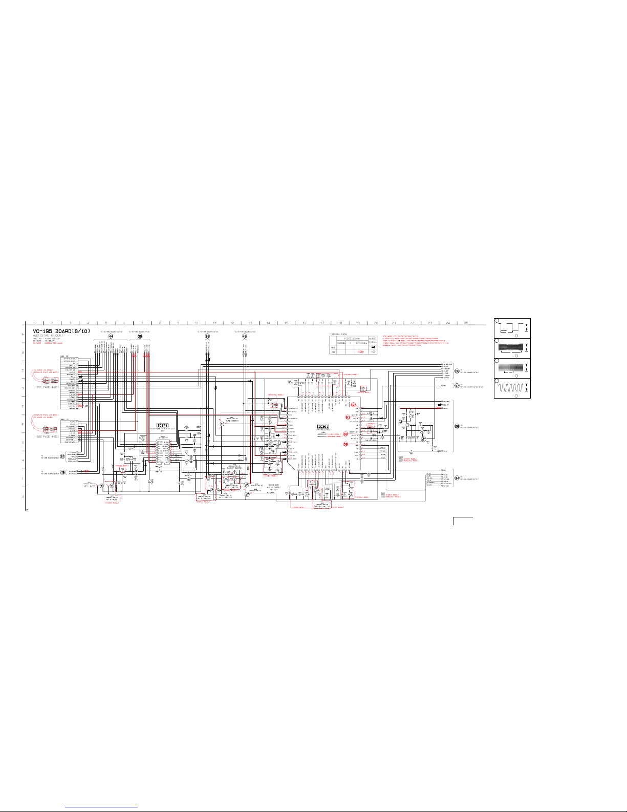
CCD-TRV3E/TRV13E/TRV23E/TRV45E/TRV55E/TRV65E/
TRV69E/TRV75/TRV75PK/TRV715
4-41 4-42
4-43
4-44
AUDIO
VC-195 (8/10)
VC-195 BOARD (8/10)
59
60
61
62
IC301 32
3.58 MHz
0.26Vp-p
2V
2.9Vp-p
IC301
21
CAMERA REC
V
0.4Vp-p
IC301
24
PB
V
0.36Vp-p
IC301
29
CAMERA REC
CAMERA REC
• For schematic diagrams.
• Refer to page 4–11 for Printed Wiring Board.
CCD-TRV3E/TRV13E/TRV23E/TRV45E/TRV55E/TRV65E/
TRV69E/TRV75/TRV75PK/TRV715
Page 66
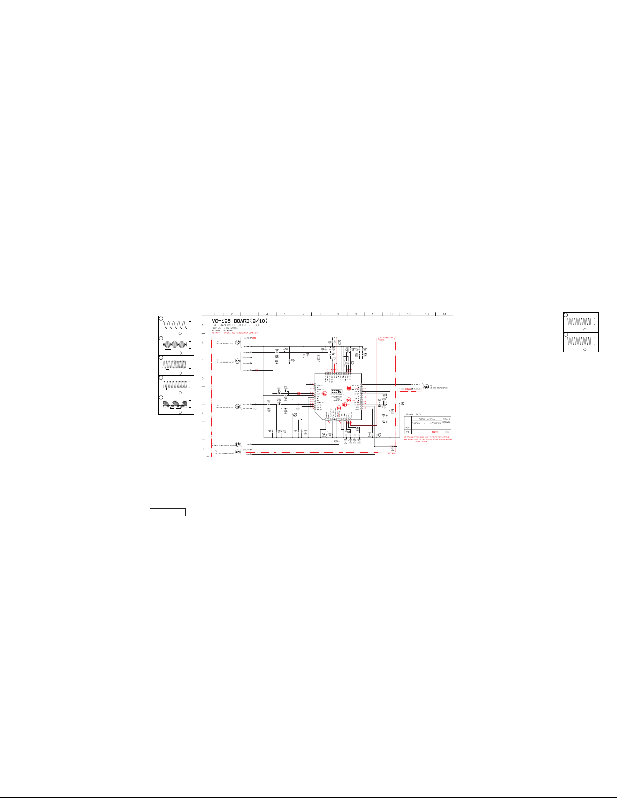
CCD-TRV3E/TRV13E/TRV23E/TRV45E/TRV55E/TRV65E/
TRV69E/TRV75/TRV75PK/TRV715
4-45
4-46
4-47
4-48
VC-195 BOARD (10/10)
68
69
IC604 41
20 MHz
1.5Vp-p
IC604 52
32 kHz
2.6Vp-p
VC-195 BOARD (9/10)
PB
2usec
0.5Vp-p
IC751
15
0.09usec
0.34Vp-p
IC751
16
0.09usec
0.7Vp-p
IC751
22
H
0.5Vp-p
IC751
41
63
64
65
66
67
IC751 7
3.58 MHz
0.25Vp-p
• For schematic diagrams.
• Refer to page 4–11 for Printed Wiring Board.
IR TRANSMITTER
VC-195 (9/10)
CCD-TRV3E/TRV13E/TRV23E/TRV45E/TRV55E/TRV65E/
TRV69E/TRV75/TRV75PK/TRV715
Page 67
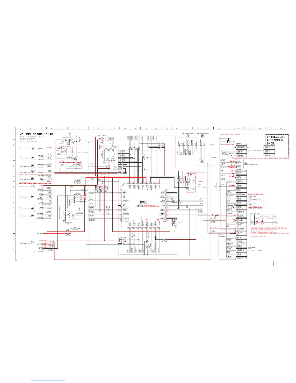
CCD-TRV3E/TRV13E/TRV23E/TRV45E/TRV55E/TRV65E/
TRV69E/TRV75/TRV75PK/TRV715
4-49 4-50
4-51
• For schematic diagrams.
• Refer to page 4–11 for Printed Wiring Board.
• Refer to page 4–48 for Waveforms.
MODE CONTROL
VC-195 (10/10)
Page 68
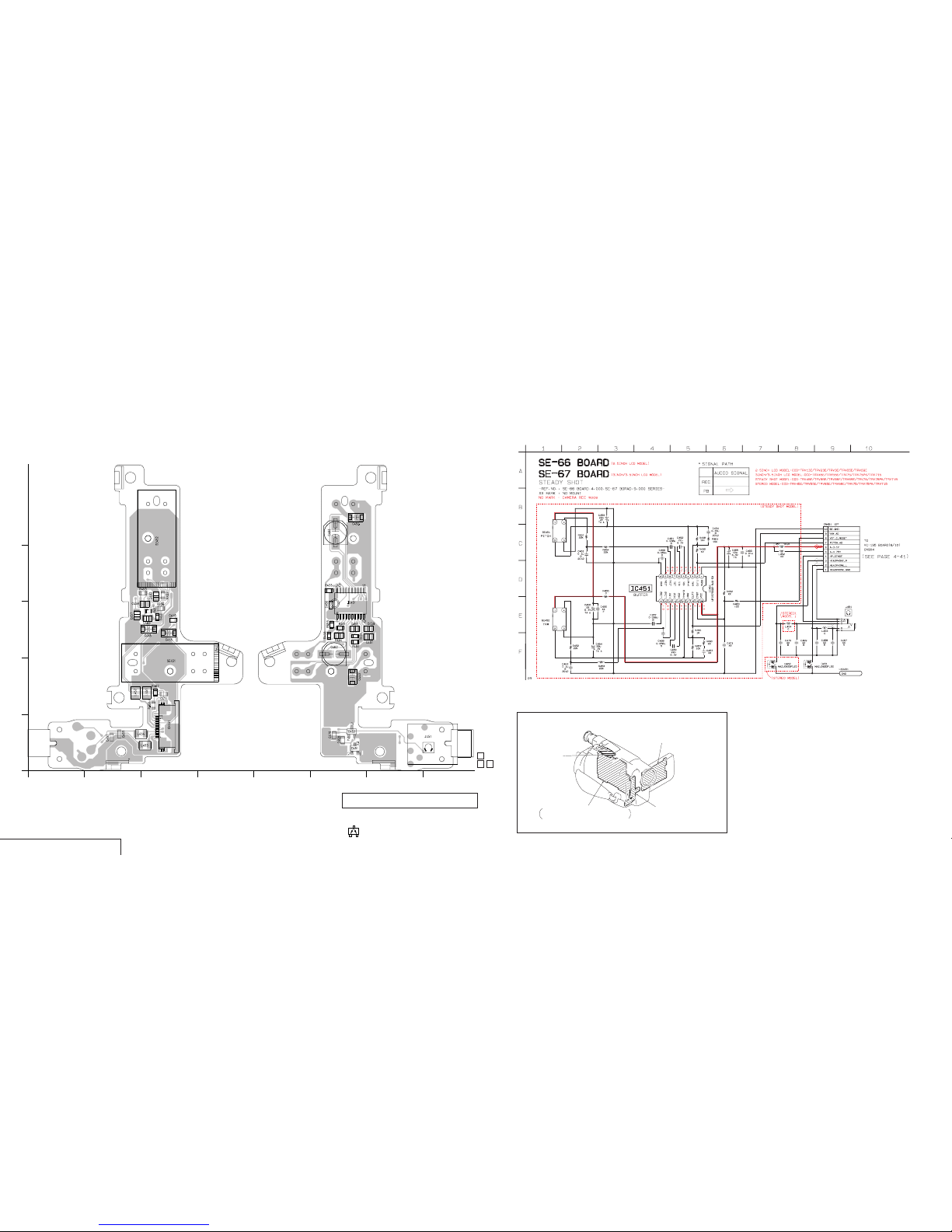
CCD-TRV3E/TRV13E/TRV23E/TRV45E/TRV55E/TRV65E/
TRV69E/TRV75/TRV75PK/TRV715
4-52
4-53 4-54
STEADY SHOT
SE-66/67 (2.5 INCH LCD, 3 INCH/3.5 INCH LCD MODEL
SE-66/67 (STEADY SHOT) (2.5 INCH LCD, 3 INCH/3.5 INCH LCD MODEL) PRINTED WIRING BOARD
– Ref No. SE-66 BOARD: 4,000 series, SE-67 BOARD: 9,000 series –
SE-66
SE-67 BOARD
C451 C-6
C452 D-3
C453 B-6
C454 E-6
C455 C-3
C456 C-3
C457 C-2
C458 C-3
C459 C-6
C460 E-6
C461 C-6
C462 C-6
C463 C-3
C464 C-6
C465 C-3
C466 C-6
C467 A-2
C468 A-6
C469 A-2
C470 A-6
C471 B-3
CN451 A-3
D451 A-6
D452 A-6
IC451 C-6
J451 A-8
L451 B-3
L452 B-2
L453 A-3
L454 A-2
R451 C-6
R452 D-3
R453 D-3
R454 C-6
R455 D-6
R456 C-3
R457 C-3
R458 C-6
R459 C-6
R460 C-3
R461 C-6
R462 B-3
R463 B-3
SE451 B-3
SE452 D-3
• For Printed Wiring Boards.
• Chip diode
3
21
There are few cases that the part isn't mounted in this model is
printed on this diagram.
12345678
A
B
C
D
E
09
SE-66 BOARD (SIDE B)
SE-67 BOARD (SIDE B)
SE-66 BOARD (SIDE A)
SE-67 BOARD (SIDE A)
1-668-947-
1-668-938-
12 22
12
VC-195
CAMERA, Y/C PROCESSOR, IN/OUT,
REC/PB HEAD AMP, SERVO/SYSTEM CONTROL,
SERVO, AUDIO, IR TRANSMITTER, MODE CONTROL
VF-99
(B/W EVF)
SE-66 (2.5 INCH LCD MODEL)
SE-67 (3 INCH/3.5 INCH LCD MODEL)
(STEADY SHOT)
PD-92 (2.5 INCH LCD MODEL)
PD-93 (3 INCH/3.5 INCH LCD MODEL)
(RGB DECODER, LCD, LCD DRIVE, BACK LIGHT)
Page 69
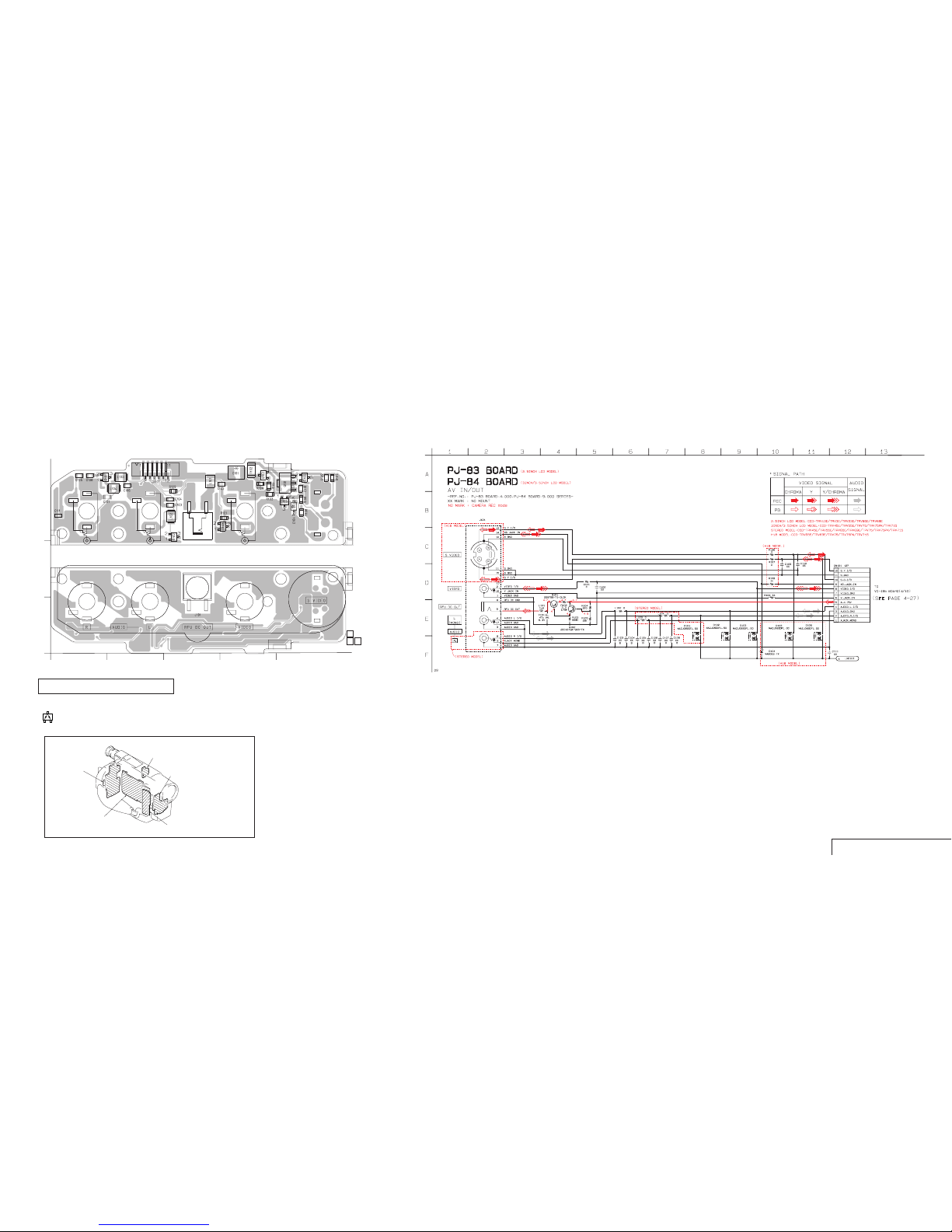
CCD-TRV3E/TRV13E/TRV23E/TRV45E/TRV55E/TRV65E/
TRV69E/TRV75/TRV75PK/TRV715
PJ-83
PJ-84 BOARD
C101 C-4
C102 C-4
C103 C-3
C104 C-3
C105 C-1
C106 C-2
C107 C-1
C108 C-1
C109 C-5
C110 C-5
C111 C-1
CN101 C-2
D101 C-1
D102 C-3
D103 C-4
D105 C-5
D106 C-5
D107 C-5
J101 A-3
L101 C-3
L102 C-3
L103 C-2
L104 C-2
Q101 C-5
Q102 C-4
R101 C-4
R102 C-4
R103 C-4
R104 C-4
R105 C-4
R106 C-5
R107 C-5
R108 C-5
R109 C-3
4-55 4-56
4-57
AV IN/OUT
PJ-83/84 (2.5 INCH LCD, 3 INCH/3.5 INCH LCD MODEL
PJ-83/84 (AV IN/OUT) (2.5 INCH LCD, 3 INCH/3.5 INCH LCD MODEL) PRINTED WIRING BOARD
– Ref No. PJ-83 BOARD: 4,000 series, PJ-84 BOARD: 9,000 series –
• For Printed Wiring Boards.
• Chip diode
There are few cases that the part isn't mounted in this model is
printed on this diagram.
3
21
1234 5
A
B
C
09
PJ-83 BOARD (SIDE B)
PJ-84 BOARD (SIDE B)
PJ-83 BOARD (SIDE A)
PJ-84 BOARD (SIDE A)
1-668-9371-668-946-
12
12 22
CD-197 (2.5 INCH LCD MODEL)
CD-198 (3 INCH/3.5 INCH LCD MODEL)
(CCD IMAGER)
PJ-83 (2.5 INCH LCD MODEL)
PJ-84 (3 INCH/3.5 INCH LCD MODEL)
(AV IN/OUT)
MA-331 (2.5 INCH LCD MODEL)
MA-312 (3 INCH/3.5 INCH LCD MODEL)
(STEREO MIC, LASER LINK)
CF-50 (2.5 INCH LCD MODEL)
CF-51 (3 INCH/3.5 INCH LCD MODEL)
(CONTROL)
DD-105
(POWER)
Page 70
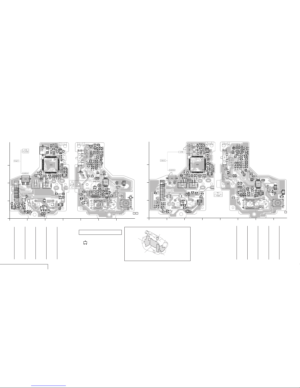
CCD-TRV3E/TRV13E/TRV23E/TRV45E/TRV55E/TRV65E/
TRV69E/TRV75/TRV75PK/TRV715
STEREO MIC, LASER LINK
MA-331 (2.5 INCH LCD MODEL), MA312 (3 INCH/3.5 INCH LCD MODEL)
4-58
4-59
4-60
MA-331 (STEREO MIC, LASER LINK) (2.5 INCH LCD MODEL) PRINTED WIRING BOARDS
– Ref No. MA-331 BOARD: 4,000 series –
12345678
A
B
C
D
09
MA-312 BOARD (SIDE B) MA-312 BOARD (SIDE A)
1-668-940-
12
MA-312 (STEREO MIC, LASER LINK) (3 INCH/3.5 INCH LCD MODEL) PRINTED
WIRING BOARD
– Ref No. MA-312 BOARD: 9,000 series –
• For Printed Wiring Boards.
• Chip transistor
There are few cases that the part isn't mounted in this model is
printed on this diagram.
C
Q
BE
1234567
A
B
C
D
09
MA-331 BOARD (SIDE B) MA-331 BOARD (SIDE A)
1-668-949-
12 22
MA-331 BOARD
C301 A-3
C302 A-3
C303 A-1
C304 A-2
C305 A-2
C306 A-1
C321 B-5
C322 B-5
C323 B-5
C324 B-6
C325 B-6
C326 B-6
C327 B-5
C328 B-6
C329 B-6
C330 C-7
C331 B-6
C332 B-6
C333 C-3
C334 C-3
C335 C-3
C336 D-3
C337 C-4
C338 C-3
C339 C-3
C340 C-5
C341 C-3
C342 C-4
C343 C-3
C344 B-5
C345 C-5
C346 D-4
C347 C-3
C348 D-3
C349 D-3
C350 D-3
C351 D-3
C352 D-3
C353 D-3
C354 D-5
C355 D-5
C356 C-2
C357 C-2
C358 D-5
C359 C-5
C360 C-2
C361 C-2
C362 D-5
C363 D-6
C364 D-6
C365 D-5
C366 D-5
C367 D-6
C368 D-6
C369 C-6
C370 D-6
C371 C-2
C372 D-3
C373 D-5
C374 B-6
C375 D-5
C376 B-7
C377 B-6
C378 C-6
CN301 B-2
CN302 B-3
CN303 B-1
D301 A-6
D302 A-6
D303 B-5
D305 B-7
D307 D-5
D308 B-7
D309 A-5
D322 B-5
D323 B-6
IC301 A-7
IC321 C-6
IC322 D-3
J310 B-5
L301 B-1
Q301 A-5
Q302 A-1
Q303 A-2
Q304 B-3
Q305 A-1
Q321 B-5
Q322 B-6
R301 A-5
R302 A-1
R303 A-2
R304 A-3
R305 A-2
R306 B-7
R307 B-1
R308 D-3
R309 D-3
R310 B-3
R311 A-1
R312 B-5
R313 B-5
R314 A-1
R315 A-1
R321 C-5
R322 B-3
R323 A-4
R324 C-5
R325 B-5
R326 B-5
R327 B-5
R328 B-5
R329 B-5
R330 B-6
R331 B-6
R332 B-6
R333 B-6
R334 B-6
R335 C-4
R336 C-4
R337 C-3
R338 D-3
R339 C-5
R340 C-3
R341 C-5
R342 C-3
R343 C-5
R344 C-5
R345 D-3
R346 C-3
R347 D-3
R348 D-5
R349 D-5
R350 D-5
R351 D-5
R352 C-2
R353 D-5
R354 D-5
R355 D-5
R356 D-6
R357 D-6
R358 D-5
R359 C-2
R360 C-6
R361 D-5
R362 D-6
R363 D-5
R364 D-5
R365 C-5
R366 C-5
R367 C-5
R368 D-5
S301 D-4
S302 D-2
S303 C-1
MA-312 BOARD
C301 A-3
C302 A-3
C303 A-1
C304 A-1
C305 A-3
C306 B-8
C321 B-6
C322 B-6
C323 B-6
C324 B-6
C325 B-7
C326 B-7
C327 B-6
C328 B-6
C329 B-6
C330 C-7
C331 B-7
C332 B-6
C333 C-4
C334 C-4
C335 C-4
C336 D-4
C337 C-4
C338 C-4
C339 C-3
C340 C-6
C341 C-6
C342 C-4
C343 C-4
C344 C-3
C345 C-3
C346 D-4
C347 C-3
C348 D-3
C349 D-3
C350 D-4
C351 D-4
C352 D-4
C353 D-3
C354 D-5
C355 D-6
C356 C-3
C357 C-3
C358 C-6
C359 D-6
C360 C-3
C361 C-2
C362 D-6
C363 D-6
C364 D-6
C365 D-6
C366 D-6
C367 D-6
C368 D-6
C369 C-6
C370 D-6
C371 D-5
C372 D-5
C373 D-5
C374 C-6
C375 D-5
C376 B-8
C377 B-3
C378 C-6
CN301 B-2
CN302 B-3
CN303 B-1
D301 A-6
D302 A-7
D303 B-5
D305 B-8
D307 D-3
D308 B-7
D321 C-5
D322 B-3
D323 B-7
F301 B-2
IC301 A-8
IC321 B-7
IC332 C-3
J301 B-5
L301 B-2
Q301 A-2
R329 B-6
R330 B-6
R331 B-6
R332 B-7
R333 B-7
R334 B-6
R335 C-4
R336 D-4
R337 C-4
R338 D-4
R339 C-5
R340 C-2
R341 C-5
R342 C-3
R343 C-5
R344 C-5
R345 D-3
R346 C-3
R347 D-3
R348 D-3
R349 D-5
R350 D-5
R351 C-6
R351 D-6
R352 C-3
R353 D-6
R354 D-6
R355 D-6
R356 D-6
R358 D-6
Q302 A-1
Q303 A-2
Q304 B-3
Q305 A-1
Q321 B-6
Q322 B-6
R301 A-2
R302 B-1
R303 A-1
R304 A-3
R305 A-3
R306 B-8
R307 B-7
R308 D-4
R309 D-4
R310 B-3
R311 B-1
R312 A-6
R313 B-6
R314 A-1
R315 A-1
R321 C-5
R322 B-3
R323 B-3
R324 B-6
R325 B-6
R326 B-6
R327 B-6
R328 B-6
R359 C-2
R360 C-6
R361 D-6
R362 D-6
R363 D-6
R364 D-6
R365 C-6
R366 C-6
R367 C-6
R368 D-5
S301 D-5
S302 D-3
S303 C-2
CD-197 (2.5 INCH LCD MODEL)
CD-198 (3 INCH/3.5 INCH LCD MODEL)
(CCD IMAGER)
PJ-83 (2.5 INCH LCD MODEL)
PJ-84 (3 INCH/3.5 INCH LCD MODEL)
(AV IN/OUT)
MA-331 (2.5 INCH LCD MODEL)
MA-312 (3 INCH/3.5 INCH LCD MODEL)
(STEREO MIC, LASER LINK)
CF-50 (2.5 INCH LCD MODEL)
CF-51 (3 INCH/3.5 INCH LCD MODEL)
(CONTROL)
DD-105
(POWER)
Page 71
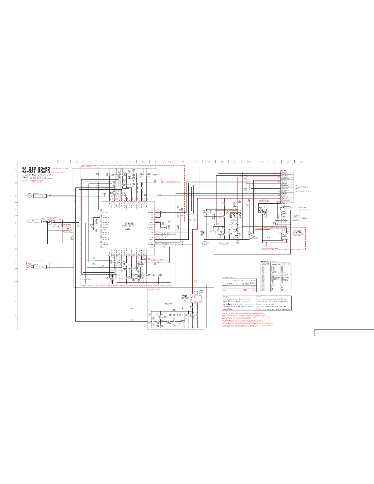
CCD-TRV3E/TRV13E/TRV23E/TRV45E/TRV55E/TRV65E/
TRV69E/TRV75/TRV75PK/TRV715
4-62
4-61
4-63 STEREO MIC, LASER LINK
MA-331 (2.5 INCH LCD MODEL), MA312 (3 INCH/3.5 INCH LCD MODEL)
Page 72
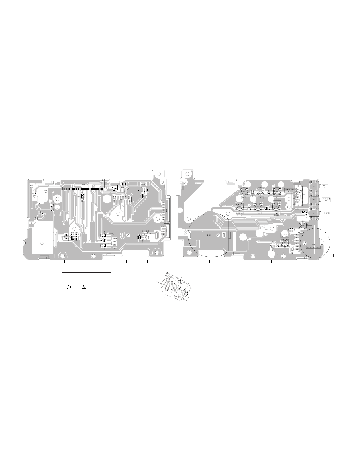
CCD-TRV3E/TRV13E/TRV23E/TRV45E/TRV55E/TRV65E/
TRV69E/TRV75/TRV75PK/TRV715
CF-50 BOARD
BH001 B-10
C001 B-6
C002 B-6
CN001 D-3
CN002 A-5
CN003 D-6
CN005 C-7
CN006 B-7
CN007 C-5
CN008 D-5
D001 D-6
D003 D-12
D004 A-13
D005 B-7
D006 B-6
D007 A-14
D008 B-6
D009 B-1
D102 A-4
Q001 D-5
Q002 C-1
Q003 B-3
Q005 B-2
R001 B-1
R002 B-13
R003 B-3
R005 A-13
R006 C-3
R007 D-3
R008 D-3
R009 D-1
R013 A-13
R015 C-14
R016 D-12
R019 C-14
R020 C-12
R023 B-14
R025 D-1
R026 C-12
R029 C-2
R031 B-4
R032 C-11
R036 C-2
R038 B-4
R039 C-2
R041 A-4
R049 B-3
R050 B-3
R051 B-3
R052 B-3
R053 A-4
S003 D-11
S004 C-15
S006 A-13
S008 D-13
S010 B-14
S012 C-15
S013 C-13
S015 A-15
S017 D-15
S018 C-12
S021 D-12
S022 C-11
S024 D-24
CF-50 (CONTROL (2.5 INCH LCD MODEL)) PRINTED WIRING BOARD
– Ref No. CF-50 BOARD: 4,000 series –
CONTROL
CF-50 (2.5 INCH LCD MODEL)
• For Printed Wiring Boards.
• Chip transistor Chip diode
There are few cases that the part isn't mounted in this model is
printed on this diagram.
C
Q
BE
1234567891011
A
B
C
D
09
CF-50 BOARD (SIDE B)
1-668-950-
12 22
12 13 14 15
CF-50 BOARD (SIDE A)
3
21
CD-197 (2.5 INCH LCD MODEL)
CD-198 (3 INCH/3.5 INCH LCD MODEL)
(CCD IMAGER)
PJ-83 (2.5 INCH LCD MODEL)
PJ-84 (3 INCH/3.5 INCH LCD MODEL)
(AV IN/OUT)
MA-331 (2.5 INCH LCD MODEL)
MA-312 (3 INCH/3.5 INCH LCD MODEL)
(STEREO MIC, LASER LINK)
CF-50 (2.5 INCH LCD MODEL)
CF-51 (3 INCH/3.5 INCH LCD MODEL)
(CONTROL)
DD-105
(POWER)
4-64 4-65
4-66
Page 73
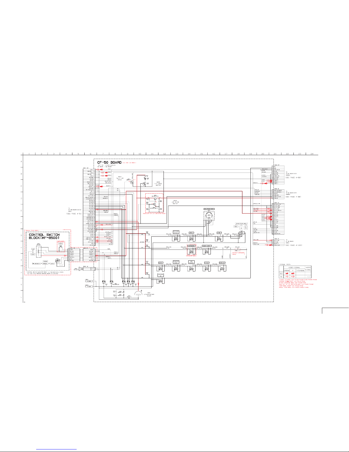
CCD-TRV3E/TRV13E/TRV23E/TRV45E/TRV55E/TRV65E/
TRV69E/TRV75/TRV75PK/TRV715
4-67 4-68
4-69
CONTROL
CF-50 (2.5 INCH LCD MODEL)
Page 74
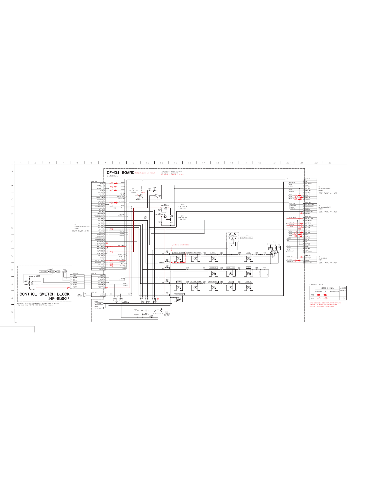
CCD-TRV3E/TRV13E/TRV23E/TRV45E/TRV55E/TRV65E/
TRV69E/TRV75/TRV75PK/TRV715
4-724-71
4-70
CONTROL
CF-51 (3 INCH/3.5 INCH LCD MODEL)
Page 75
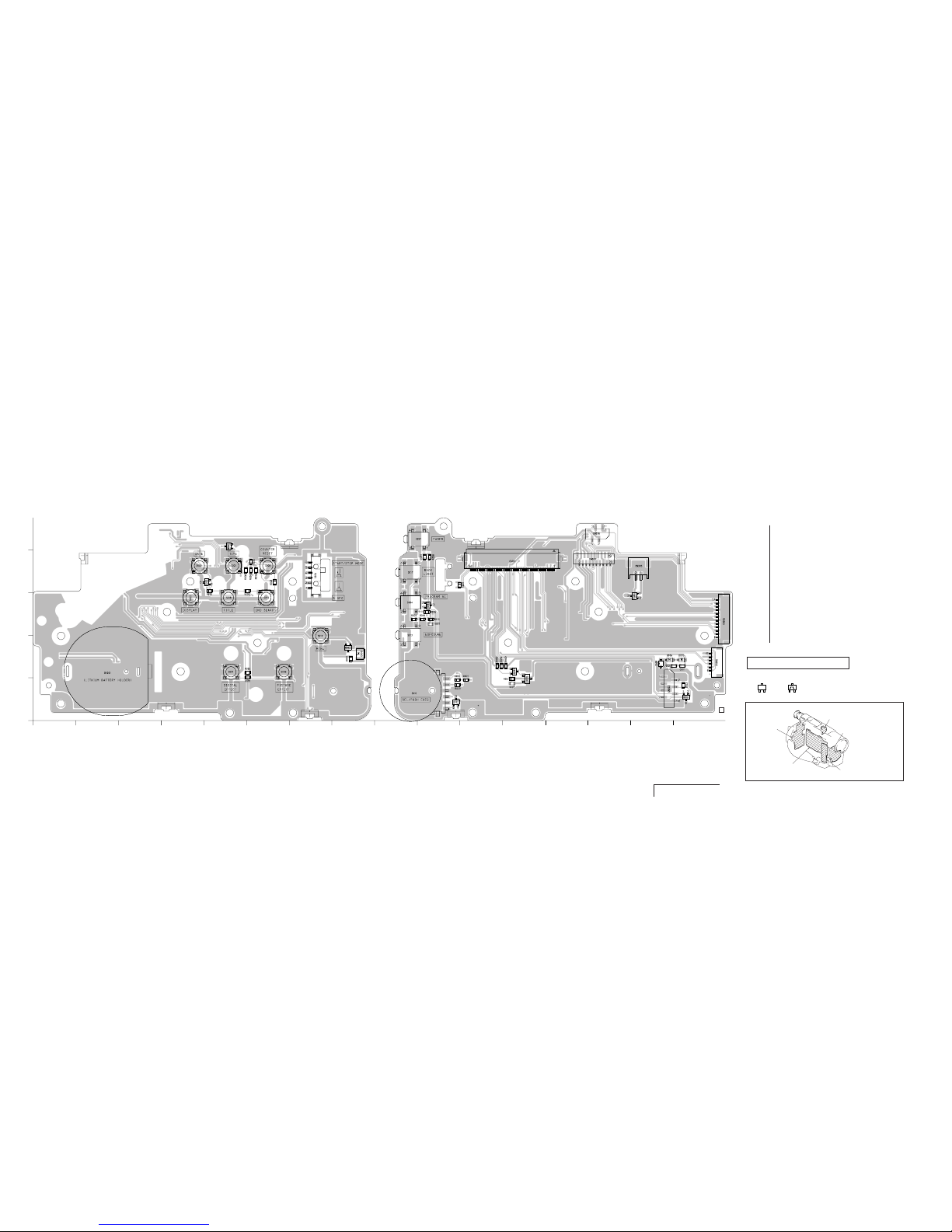
CCD-TRV3E/TRV13E/TRV23E/TRV45E/TRV55E/TRV65E/
TRV69E/TRV75/TRV75PK/TRV715
4-73 4-74
4-75
4-76
CONTROL
CF-51 (3 INCH/3.5 INCH LCD MODEL)
CF-51 (CONTROL (3 INCH/3.5 INCH LCD MODEL) PRINTED WIRING BOARD
– Ref No. CF-51 BOARD: 9,000 series –
• For Printed Wiring Boards.
• Chip transistor Chip diode
There are few cases that the part isn't mounted in this model is
printed on this diagram.
C
Q
BE
CF-51 BOARD
BH001 B-2
C001 B-16
C002 B-15
CN001 D-12
CN002 A-15
CN003 D-15
CN005 C-16
CN006 B-16
CN007 D-14
CN008 E-14
D001 C-15
D003 D-5
D004 C-10
D005 B-16
D006 B-15
D007 A-10
D008 B-15
D009 B-8
D012 A-16
Q001 E-5
Q002 B-8
Q003 B-12
Q005 A-12
R001 B-8
R003 A-12
R005 B-5
R006 D-6
R007 C-10
R008 D-6
R009 C-10
R013 B-5
R015 C-10
R018 D-6
R019 C-10
R020 D-6
R022 A-11
R023 A-10
R029 A-10
R031 D-10
R038 D-5
R038 D-10
R039 D-10
R041 A-16
R049 B-12
R050 B-11
R051 A-12
R052 B-11
S001 B-5
S002 C-4
S003 D-4
S004 C-9
S006 B-6
S008 D-6
S010 B-7
S012 C-9
S013 C-6
S015 A-9
S017 D-9
S018 C-5
S021 D-5
S024 D-7
S025 C-9
S027 E-10
3
21
1234567891011
A
B
C
D
E
09
CF-51 BOARD (SIDE B) CF-51 BOARD (SIDE A)
1-668-941-
12
12 13 14 15 16
CCD-TRV3E/TRV13E/TRV23E/TRV45E/TRV55E/TRV65E/
TRV69E/TRV75/TRV75PK/TRV715
CD-197 (2.5 INCH LCD MODEL)
CD-198 (3 INCH/3.5 INCH LCD MODEL)
(CCD IMAGER)
PJ-83 (2.5 INCH LCD MODEL)
PJ-84 (3 INCH/3.5 INCH LCD MODEL)
(AV IN/OUT)
MA-331 (2.5 INCH LCD MODEL)
MA-312 (3 INCH/3.5 INCH LCD MODEL)
(STEREO MIC, LASER LINK)
CF-50 (2.5 INCH LCD MODEL)
CF-51 (3 INCH/3.5 INCH LCD MODEL)
(CONTROL)
DD-105
(POWER)
Page 76
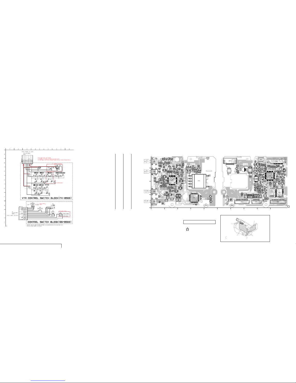
CCD-TRV3E/TRV13E/TRV23E/TRV45E/TRV55E/TRV65E/
TRV69E/TRV75/TRV75PK/TRV715
4-78 4-79
4-80
PD-92 (RGB DECODER, LCD DRIVE, BACK LIGHT, LCD (2.5 INCH LCD MODEL)) PRINTED WIRING BOARD
– Ref No. PD-92 BOARD: 10,000 series –
CONTROL SWITCH BLOCK, RGB DECODER, LCD DRIVE, BACK LIGHT, LCD
PD-92 (2.5 INCH LCD MODEL)
FK-8500, SS-8500
4-77
PD-92 BOARD
C5501 B-10
C5502 B-10
C5503 C-2
C5504 C-10
C5505 C-10
C5506 B-2
C5507 C-3
C5508 B-2
C5509 C-3
C5510 C-1
C5511 C-2
C5512 C-1
C5513 C-1
C5514 C-2
C5515 C-2
C5516 C-2
C5517 C-1
C5518 C-3
C5519 B-2
C5520 C-3
C5601 A-2
C5602 A-2
C5603 B-10
C5604 C-9
C5605 C-9
C5607 B-9
C5608 C-9
C5609 B-10
C5610 C-9
C5611 B-8
C5612 C-10
C5613 B-8
C5614 C-10
C5615 C-10
C5616 C-9
C5618 D-9
C5619 D-2
C5620 D-10
C5622 C-10
C5623 C-2
C5624 B-3
C5625 B-2
C5633 B-9
C5634 B-9
C5701 C-8
C5702 C-8
C5703 C-3
C5704 C-7
C5705 C-6
C5706 C-4
C5801 C-4
C5821 C-1
CN5501 D-9
CN5601 D-10
CN5701 D-6
CN5801 C-8
CN5802 C-7
CN5803 C-8
CN5804 C-10
CN5805 C-6
D5601 B-10
D5602 B-9
D5603 B-10
D5605 B-9
D5604 C-10
D5701 C-5
D5702 C-5
D5703 D-5
D5704 C-7
IC5501 B-10
IC5502 C-2
IC5601 C-9
IC5602 C-8
IC5701 C-4
IC5801 C-4
L5501 C-3
L5502 A-2
L5503 A-2
L5601 A-2
L5603 C-9
L5604 A-2
L5605 C-9
L5701 C-7
Q5501 C-2
Q5601 B-9
Q5602 B-9
Q5603 B-10
Q5604 C-10
Q5605 C-8
Q5606 C-9
Q5607 C-9
Q5608 C-8
Q5609 B-9
Q5701 C-3
Q5702 C-4
R5501 B-2
R5502 B-2
R5504 B-2
R5505 B-2
R5506 B-2
R5507 B-2
R5508 B-1
R5508 B-2
R5509 B-1
R5510 B-3
R5511 B-3
R5512 B-1
R5513 B-2
R5516 B-2
R5517 B-1
R5518 B-1
R5519 C-3
R5520 C-3
R5521 B-2
R5522 B-2
R5523 C-3
R5526 C-1
R5527 B-1
R5528 C-3
R5529 C-1
R5530 B-1
R5531 C-2
R5532 C-3
R5533 B-1
R5537 D-8
R5541 D-2
R5542 D-3
R5544 C-2
R5546 C-2
R5546 D-2
R5602 C-2
R5603 D-8
R5604 D-3
R5605 C-1
R5606 C-10
R5607 A-2
R5609 C-9
R5610 B-10
R5612 C-9
R5614 C-9
R5615 C-9
R5616 B-10
R5617 B-9
R5618 C-9
R5619 B-9
R5620 B-9
R5621 C-9
R5622 B-8
R5623 B-8
R5624 B-9
R5625 C-10
R5626 C-9
R5627 C-10
R5628 C-10
R5629 B-9
R5630 B-9
R5631 C-9
R5632 B-9
R5634 B-9
R5635 C-10
R5636 B-10
R5637 C-10
R5638 C-10
R5639 C-1
R5640 C-8
R5641 C-3
R5642 C-10
R5644 C-9
R5645 C-10
R5646 C-10
R5647 D-2
R5648 C-3
R5648 D-10
R5651 D-2
R5652 D-2
R5653 D-9
R5654 D-9
R5657 C-9
R5658 D-9
R5659 D-10
R5660 D-10
R5661 D-10
R5663 C-9
R5664 D-10
R5665 D-1
R5665 D-10
R5667 D-1
R5668 D-1
R5669 D-1
R5670 D-1
R5671 D-9
R5672 D-9
R5673 D-1
R5674 D-2
R5676 D-1
R5678 D-9
R5679 D-2
R5680 D-2
R5681 D-2
R5682 D-1
R5683 D-2
R5684 D-2
R5685 D-3
R5686 D-3
R5688 C-9
R5692 C-9
R5694 B-9
R5695 B-9
R5695 D-10
R5697 C-10
R5698 B-9
R5698 D-9
R5701 C-5
R5702 C-5
R5703 C-4
R5704 C-4
R5705 C-4
R5706 C-4
R5707 C-7
R5708 D-4
R5709 D-7
R5710 D-4
R5801 C-1
R5802 C-1
R5803 A-1
R5804 A-1
R5805 C-6
R5806 A-1
R5807 B-7
R5808 B-9
R5809 C-7
R5810 B-9
R5811 C-4
R5812 C-4
S5801 D-1
S5802 C-1
S5803 B-1
S5804 A-1
T5701 C-4
• For Printed Wiring Boards.
• This board is four-layer print board. However, the patterns of
layers 2 to 3 have not been included in the diagram.
• Chip transistor
There are few cases that the part isn't mounted in this model is
printed on this diagram.
C
Q
BE
12345678910
A
B
C
D
09
PD-92 BOARD (SIDE B) PD-92 BOARD (SIDE A)
1-668-951-
11
15
1
2
45
6
7
8
3
9
10
11
12
13
14
VC-195
CAMERA, Y/C PROCESSOR, IN/OUT,
REC/PB HEAD AMP, SERVO/SYSTEM CONTROL,
SERVO, AUDIO, IR TRANSMITTER, MODE CONTROL
VF-99
(B/W EVF)
SE-66 (2.5 INCH LCD MODEL)
SE-67 (3 INCH/3.5 INCH LCD MODEL)
(STEADY SHOT)
PD-92 (2.5 INCH LCD MODEL)
PD-93 (3 INCH/3.5 INCH LCD MODEL)
(RGB DECODER, LCD, LCD DRIVE, BACK LIGHT)
Page 77
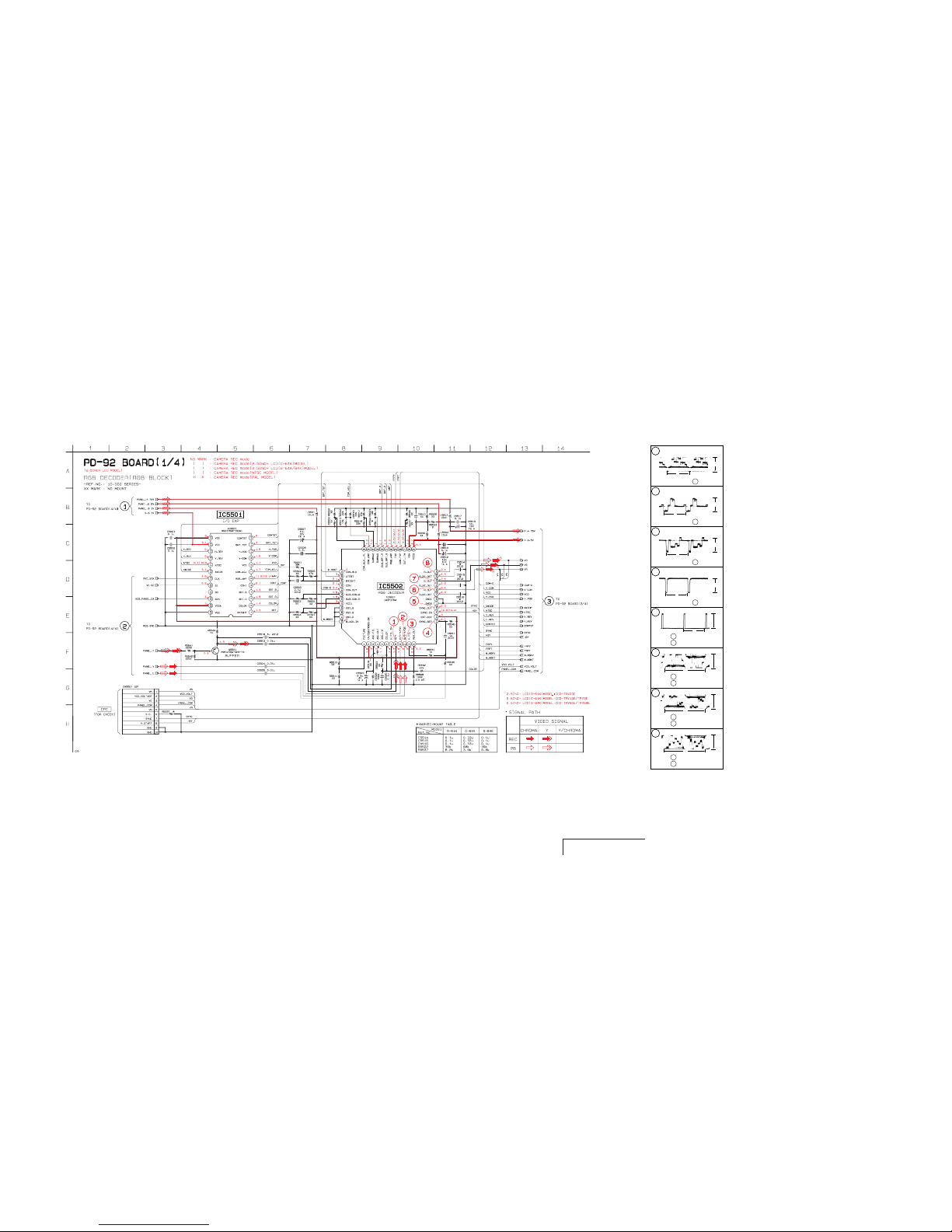
CCD-TRV3E/TRV13E/TRV23E/TRV45E/TRV55E/TRV65E/
TRV69E/TRV75/TRV75PK/TRV715
4-81
4-82
4-83
RGB DECODER
PD-92 (1/4) (2.5 INCH LCD MODEL)
PD-92 BOARD (1/4)
CAMERA REC
H
0.44Vp-p
IC5502
8
H
0.2Vp-p
IC5502
9
H
0.2Vp-p
IC5502
10
H
0.7Vp-p
IC5502
13
1
2
3
4
5
6
7
8
H
IC5502
16
IC5502
16
(
C-61K MODEL
:
3Vp-p
)
(
S-61K MODEL
:
4.7Vp-p
)
2H
IC5502
20
IC5502
20
(
C-61K MODEL
:
3.6Vp-p
)
(
S-61K MODEL
:
4.2Vp-p
)
2H
IC5502
22
IC5502
22
(
C-61K MODEL
:
3.6Vp-p
)
(
S-61K MODEL
:
4.2Vp-p
)
2H
IC5502
24
IC5502
24
(
C-61K MODEL
:
3.6Vp-p
)
(
S-61K MODEL
:
4.2Vp-p
)
CCD-TRV3E/TRV13E/TRV23E/TRV45E/TRV55E/TRV65E/
TRV69E/TRV75/TRV75PK/TRV715
Page 78
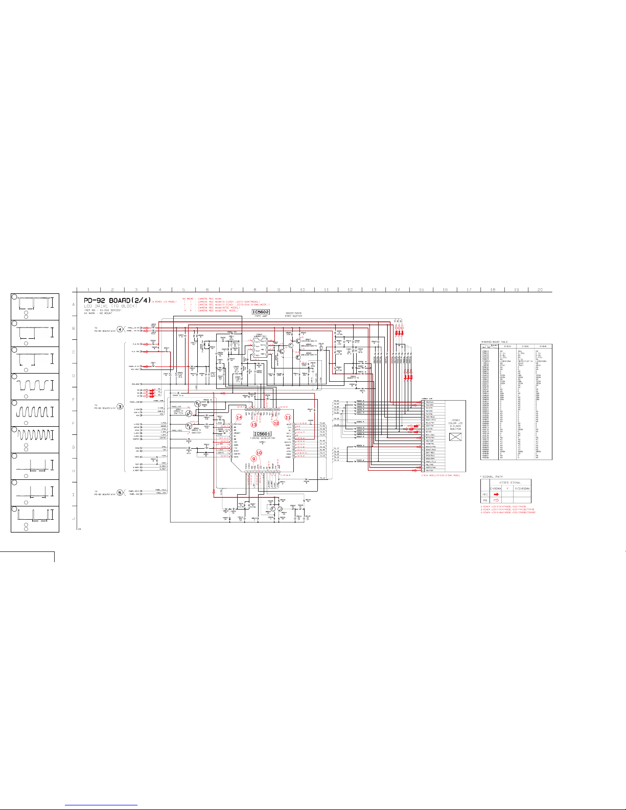
CCD-TRV3E/TRV13E/TRV23E/TRV45E/TRV55E/TRV65E/
TRV69E/TRV75/TRV75PK/TRV715
4-84
4-85 4-86
PD-92 BOARD (2/4)
CAMERA REC
9
10
10
11
11
12
13
13
14
H
IC5601
4
IC5601
4
(
C-61K
:
3Vp-p
)
(
S-61K
:
4.7Vp-p
)
V
IC5601
5
(
C-61K
:
3Vp-p
)
20msec
IC5601
5
(
S-61K
:
4.7Vp-p
)
Approx. 2.9MHz
Approx. 2.9MHz
Approx. 5.8MHz
IC5601
24
(
C-61K
:
3.4Vp-p
)
IC5601
24
(
S-61K
:
4.7Vp-p
)
IC5601
26
IC5601
26
(
C-61K : 3.2Vp-p
)
(
S-61K : 4.1Vp-p
)
V
IC5601
34
(
C-61K
:
3Vp-p
)
20msec
IC5601
34
(
S-61K
:
4.7Vp-p
)
H
IC5601
37
IC5601
37
(
C-61K
:
3Vp-p
)
(
S-61K
:
4.7Vp-p
)
LCD DRIVE
PD-92 (2/4) (2.5 INCH LCD MODEL)
• For schematic diagrams.
• Refer to page 4–79 for Printed Wiring Board.
Page 79
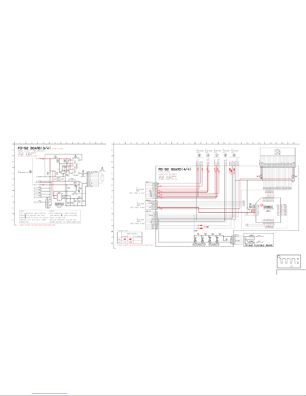
CCD-TRV3E/TRV13E/TRV23E/TRV45E/TRV55E/TRV65E/
TRV69E/TRV75/TRV75PK/TRV715
4-87 4-88 4-89
• For schematic diagrams.
• Refer to page 4–79 for Printed Wiring Board.
• For schematic diagrams.
• Refer to page 4–79 for Printed Wiring Board.
BACK LIGHT, LCD
PD-92 (3/4, 4/4) (2.5 INCH LCD MODEL)
PD-92 BOARD (4/4)
CAMERA REC
15
IC5801 2
24.17 kHz
2.9Vp-p
Page 80
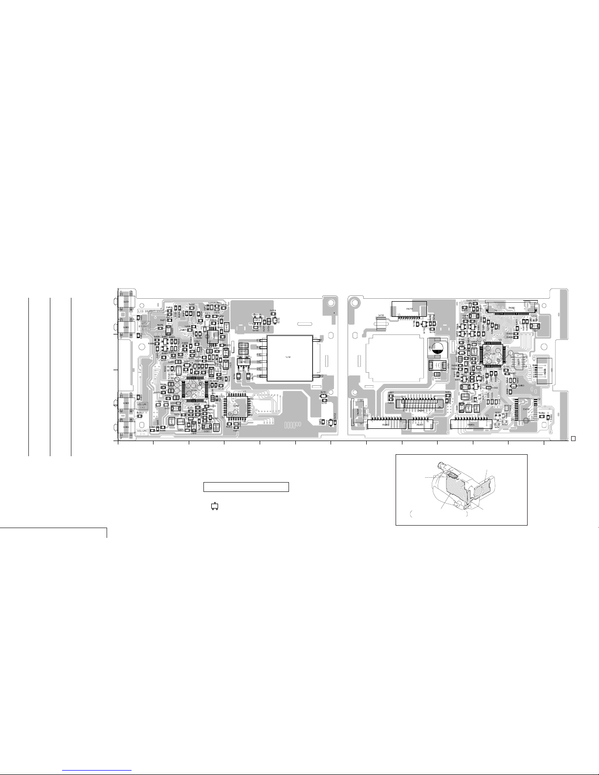
CCD-TRV3E/TRV13E/TRV23E/TRV45E/TRV55E/TRV65E/
TRV69E/TRV75/TRV75PK/TRV715
PD-93 (RGB DECODER, LCD DRIVE, BACK LIGHT, LCD (3 INCH/3.5 INCH LCD MODEL) PRINTED WIRING BOARD
– Ref No. PD-93 BOARD: 10,000 series –
RGB DECODER, LCD DRIVE, BACK LIGHT, LCD
PD-93 (3 INCH/3.5 INCH LCD MODEL)
4-90
4-91
4-92
• For Printed Wiring Boards.
• This board is four-layer print board. However, the patterns of
layers 2 to 3 have not been included in the diagram.
• Chip transistor
There are few cases that the part isn't mounted in this model is
printed on this diagram.
PD-93 BOARD
C4501 B-2
C4502 B-2
C4503 B-11
C4504 B-11
C4505 B-11
C4506 B-3
C4507 A-3
C4508 B-11
C4509 B-3
C4510 A-3
C4511 B-2
C4512 A-2
C4513 B-2
C4514 B-2
C4515 B-2
C4516 B-2
C4517 A-2
C4518 A-11
C4519 A-3
C4520 C-3
C4601 A-10
C4602 B-11
C4603 C-2
C4604 D-3
C4605 C-3
C4607 C-10
C4608 C-10
C4609 B-12
C4610 C-11
C4611 C-3
C4612 B-12
C4613 C-3
C4614 C-2
C4615 C-2
C4616 D-4
C46181 D-11
C4619 D-3
C4620 D-3
C4621 D-12
C4622 D-2
C4623 D-10
C4624 C-4
C4625 C-4
C4633 C-10
C4634 C-11
C4701 C-9
C4702 B-10
C4703 C-4
C4704 D-5
C4705 D-8
C4706 D-4
C4707 C-4
C4801 A-4
CN4501 C-12
CN4601 D-12
CN4701 D-9
CN4801 B-9
CN4802 A-8
CN4803 A-9
CN4804 A-10
CN4805 A-7
CN4806 B-12
D4601 C-2
D4602 C-10
D4603 B-12
D4605 C-10
D4614 D-12
D4701 B-6
D4702 A-6
D4704 D-5
IC4501 A-12
IC4502 B-3
IC4601 C-11
IC4602 C-3
IC4701 D-4
IC4801 A-4
L4501 A-3
L4502 A-2
L4601 A-10
L4603 B-11
L4604 A-11
L4605 C-11
L4701 C-9
Q4501 A-11
Q4601 B-11
Q4602 B-11
Q4603 C-2
Q4604 C-2
Q4605 D-10
Q4606 D-10
Q4607 D-10
Q4608 D-10
Q4609 B-11
Q4701 C-4
Q4702 D-9
R4501 B-11
R4502 B-3
R4503 B-4
R4504 B-3
R4505 B-11
R4506 B-3
R4507 B-3
R4508 A-3
R4509 A-3
R4510 B-3
R4511 B-3
R4512 A-3
R4513 A-3
R4514 C-3
R4516 A-3
R4516 C-3
R4517 A-3
R4518 A-3
R4519 B-3
R4520 B-3
R4521 A-3
R4522 A-3
R4523 C-3
R4526 A-3
R4527 A-3
R4528 B-3
R4529 A-3
R4530 A-2
R4531 C-2
R4532 A-12
R4533 A-2
R4534 B-2
R4535 B-2
R4536 B-2
R4537 C-2
R4541 A-11
R4542 A-11
R4544 A-11
R4545 C-2
R4546 B-2
R4602 C-3
R4603 D-10
R4604 D-11
R4605 A-2
R4606 A-2
R4607 A-1
R4608 C-2
R4609 B-11
R4610 C-2
R4612 B-11
R4613 B-11
R4614 C-10
R4615 B-11
R4616 B-12
R4617 B-11
R4619 B-11
R4620 C-3
R4621 C-10
R4622 C-3
R4623 C-3
R4624 C-11
R4625 B-11
R4626 C-3
R4627 B-11
R4628 C-2
R4629 C-3
R4630 C-11
R4631 C-3
R4632 B-11
R4634 C-11
R4635 C-2
R4636 C-2
R4637 C-3
R4638 C-2
R4639 C-2
R4640 D-3
R4641 C-3
R4642 C-2
R4643 D-3
R4644 D-3
R4645 C-2
R4646 C-2
R4647 C-3
R4648 C-3
R4651 D-3
R4652 D-3
R4653 D-2
R4654 D-2
R4657 D-11
R4658 D-11
R4659 D-11
R4660 D-11
R4661 D-11
R4663 D-11
R4664 D-3
R4665 D-3
R4666 D-3
R4667 D-3
R4668 C-12
R4669 D-12
R4670 D-2
R4671 D-3
R4672 D-10
R4673 D-12
R4674 D-3
R4676 D-2
R4677 D-11
R4678 D-2
R4678 D-3
R4680 D-2
R4681 D-2
R4682 D-3
R4683 D-3
R4683 D-11
R4684 D-3
R4685 C-10
R4686 D-10
R4692 B-11
R4693 C-10
R4694 C-10
R4695 C-3
R4696 D-12
R4697 D-12
R4698 D-3
R4701 B-6
R4702 A-7
R4703 B-4
R4703 D-9
R4704 B-4
R4705 D-9
R4706 D-9
R4707 D-5
R4708 D-5
R4710 D-9
R4801 D-1
R4802 C-1
R4803 B-1
R4804 A-1
R4806 A-6
R4806 A-12
R4807 B-8
R4808 B-11
R4809 B-8
R4810 B-11
R4811 A-4
R4812 A-4
S4801 D-1
S4802 D-1
S4803 B-1
S4804 A-1
T4701 C-5
C
Q
BE
1234567891011
A
B
C
D
09
PD-93 BOARD (SIDE B) PD-93 BOARD (SIDE A)
1-668-952-
11
12 13
15
1
2
3
5
6
7
8
4
9
10
11
12
13
14
VC-195
CAMERA, Y/C PROCESSOR, IN/OUT,
REC/PB HEAD AMP, SERVO/SYSTEM CONTROL,
SERVO, AUDIO, IR TRANSMITTER, MODE CONTROL
VF-99
(B/W EVF)
SE-66 (2.5 INCH LCD MODEL)
SE-67 (3 INCH/3.5 INCH LCD MODEL)
(STEADY SHOT)
PD-92 (2.5 INCH LCD MODEL)
PD-93 (3 INCH/3.5 INCH LCD MODEL)
(RGB DECODER, LCD, LCD DRIVE, BACK LIGHT)
Page 81
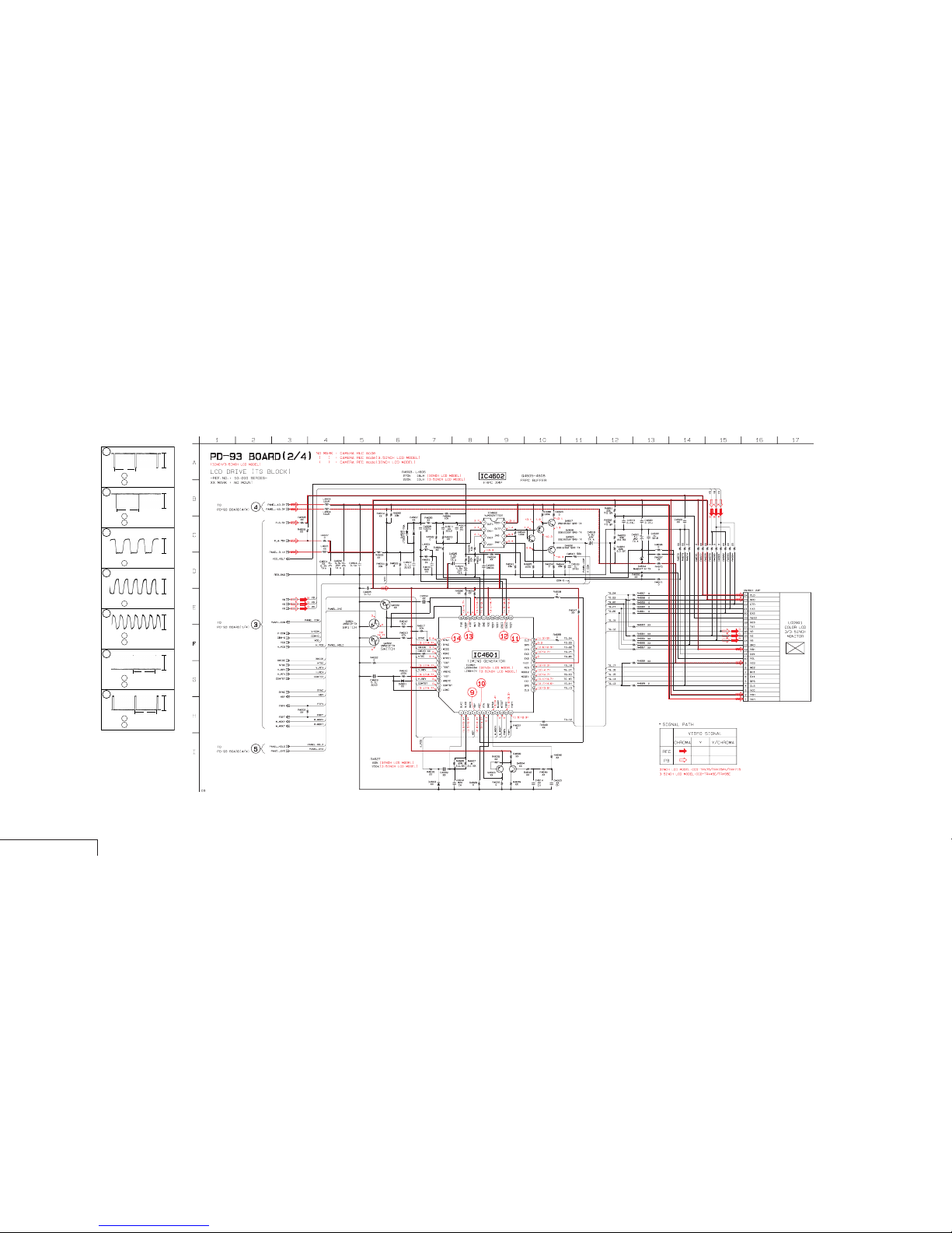
CCD-TRV3E/TRV13E/TRV23E/TRV45E/TRV55E/TRV65E/
TRV69E/TRV75/TRV75PK/TRV715
4-96
4-97
4-98
LCD DRIVE
PD-93 (2/4) (3 INCH/3.5 INCH LCD MODEL)
PD-93 BOARD (2/4)
CAMERA REC
9
10
11
11
12
13
14
V
IC4601
34
IC4601
34
(
3.5 INCH LCD : 3Vp-p
)
(
3 INCH LCD : 4.7Vp-p
)
H
IC4601
37
IC4601
37
(
3.5 INCH LCD : 3Vp-p
)
(
3 INCH LCD : 4.7Vp-p
)
H
IC4601
4
IC4601
4
(
3.5 INCH LCD : 3Vp-p
)
(
3 INCH LCD : 4.7Vp-p
)
V
IC4601
5
IC4601
5
(
3.5 INCH LCD : 3Vp-p
)
(
3 INCH LCD : 4.7Vp-p
)
Approx.3.7 MHz
IC4601
24
(
3 INCH LCD
:
4.7Vp-p
)
Approx.4.8 MHz
IC4601
24
(
3.5 INCH LCD
: 3
Vp-p
)
IC4601
26
IC4601
26
(
3.5 INCH LCD
Approx.9.5MHz / 3.3Vp-p
)
(
3 INCH LCD
Approx.7.5MHz / 4.7Vp-p
)
• For schematic diagrams.
• Refer to page 4–90 for Printed Wiring Board.
Page 82
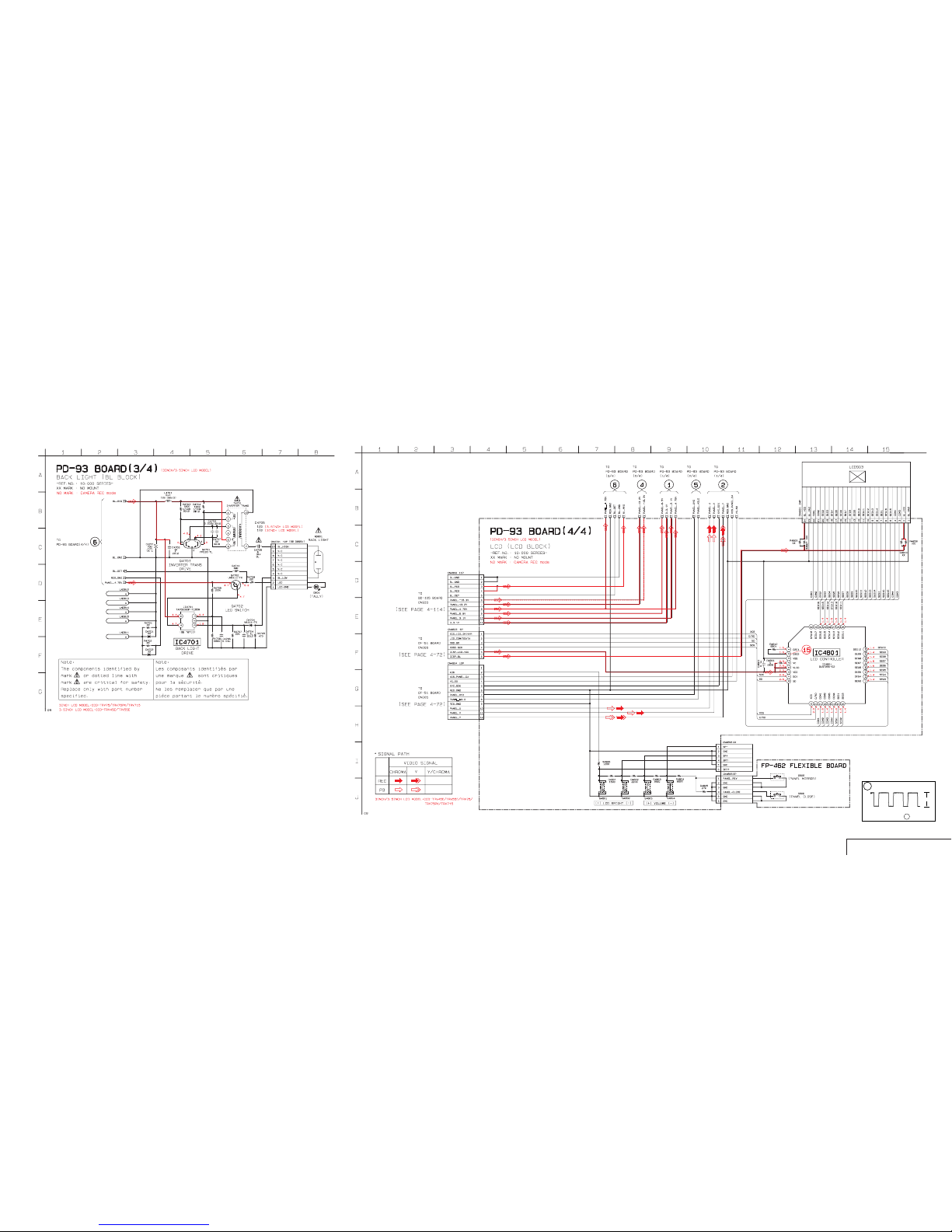
CCD-TRV3E/TRV13E/TRV23E/TRV45E/TRV55E/TRV65E/
TRV69E/TRV75/TRV75PK/TRV715
4-99 4-100 4-101
BACK LIGHT, LCD
PD-93 (3/4, 4/4) (3 INCH/3.5 INCH LCD MODEL)
• For schematic diagrams.
• Refer to page 4–90 for Printed Wiring Board.
• For schematic diagrams.
• Refer to page 4–90 for Printed Wiring Board.
PD-93 BOARD (4/4)
CAMERA REC
15
IC4801 2
24.48 kHz
2.9Vp-p
Page 83
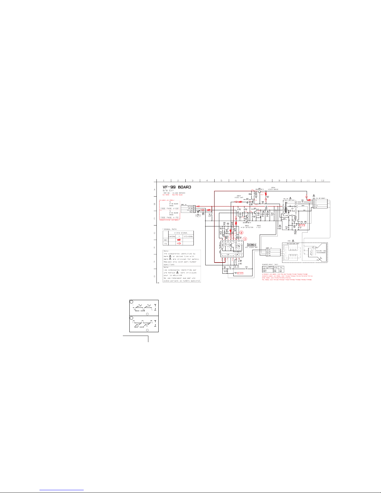
CCD-TRV3E/TRV13E/TRV23E/TRV45E/TRV55E/TRV65E/
TRV69E/TRV75/TRV75PK/TRV715
4-102
4-103 4-104
CCD-TRV3E/TRV13E/TRV23E/TRV45E/TRV55E/TRV65E/
TRV69E/TRV75/TRV75PK/TRV715
B/W EVF
VF-99 (B/W EVF MODEL)
VF-99 BOARD
CAMERA REC
H
1Vp-p
IC901
11
H
2.2Vp-p
IC901
13
1
2
Page 84
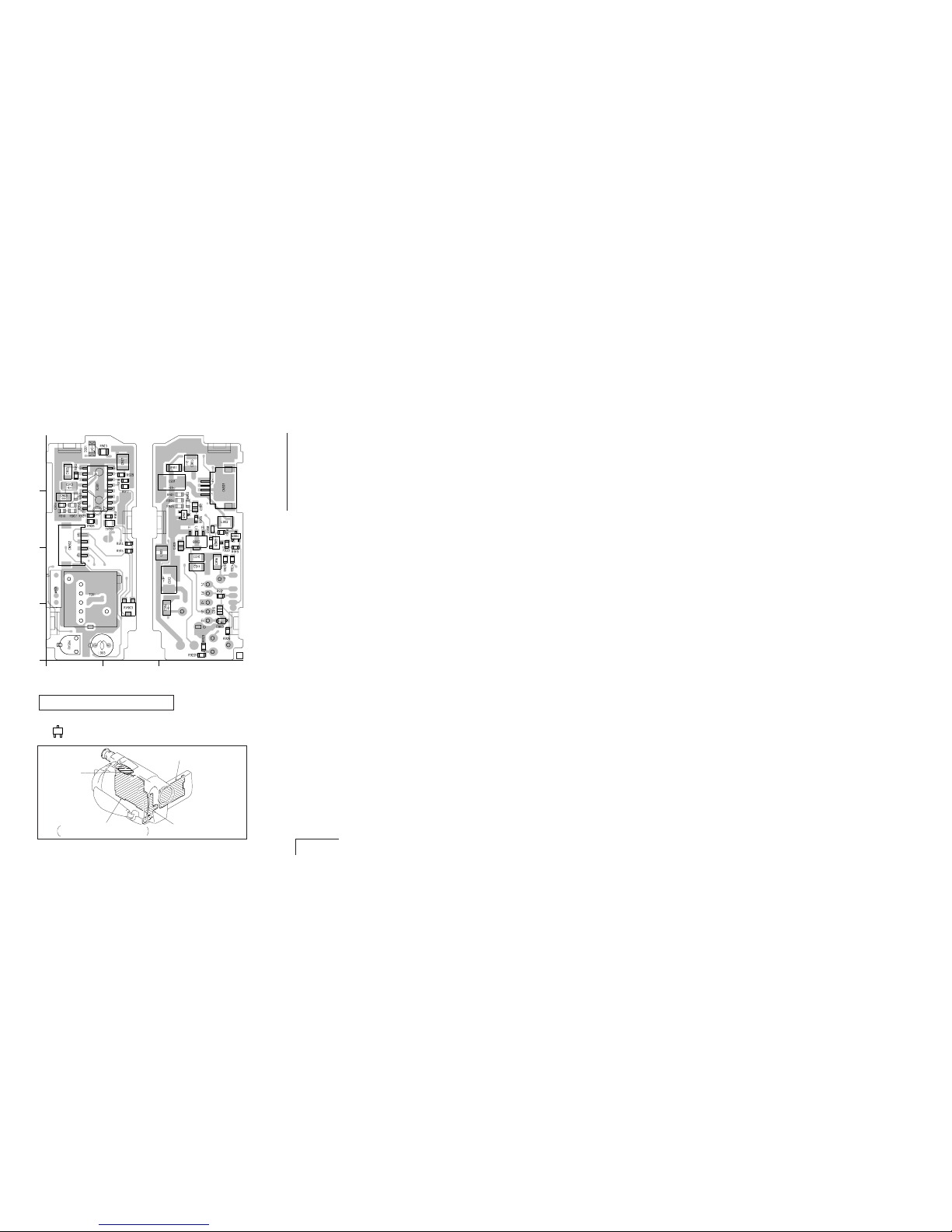
CCD-TRV3E/TRV13E/TRV23E/TRV45E/TRV55E/TRV65E/
TRV69E/TRV75/TRV75PK/TRV715
4-105 4-106 4-107
VF-99 (B/W EVF) PRINTED WIRING BOARD
– Ref No. VF-99 BOARD: 10,000 series –
• For Printed Wiring Boards.
• This board is four-layer print board. However, the patterns of
layers 2 to 3 have not been included in the diagram.
• Chip transistor
There are few cases that the part isn't mounted in this model is
printed on this diagram.
Q
C
BE
VF-99 BOARD
C901 D-3
C902 C-3
C903 C-1
C904 C-1
C905 D-3
C906 D-1
C907 D-2
C908 C-3
C909 C-3
C910 B-3
C911 B-3
C912 B-3
C913 D-1
C914 A-3
C915 A-3
C916 B-3
CN901 D-3
CN902 C-1
D901 D-1
D903 A-3
IC901 D-1
L901 B-3
L902 C-3
L903 A-1
Q901 C-3
Q902 C-3
Q903 C-3
Q904 C-3
R901 C-3
R902 C-3
R903 D-2
R904 C-3
R905 C-3
R906 C-3
R907 C-1
R908 C-1
R909 C-1
R910 C-1
R911 D-3
R912 D-1
R913 C-2
R914 C-2
R915 B-2
R916 D-2
R917 D-2
R918 C-3
R919 B-3
R920 C-3
R921 B-3
R922 A-3
R923 A-3
R924 B-3
R925 B-3
R926 A-3
R927 C-1
R928 C-1
R928 D-2
RV903 A-2
RV904 A-1
T901 B-1
TH901 C-2
W901 B-1
B/W EVF
VF-99
12 3
A
B
C
D
09
VF-99 BOARD (SIDE A) VF-99 BOARD (SIDE B)
1-660-357-
11
1
2
CCD-TRV3E/TRV13E/TRV23E/TRV45E/TRV55E/TRV65E/
TRV69E/TRV75/TRV75PK/TRV715
VC-195
CAMERA, Y/C PROCESSOR, IN/OUT,
REC/PB HEAD AMP, SERVO/SYSTEM CONTROL,
SERVO, AUDIO, IR TRANSMITTER, MODE CONTROL
VF-99
(B/W EVF)
SE-66 (2.5 INCH LCD MODEL)
SE-67 (3 INCH/3.5 INCH LCD MODEL)
(STEADY SHOT)
PD-92 (2.5 INCH LCD MODEL)
PD-93 (3 INCH/3.5 INCH LCD MODEL)
(RGB DECODER, LCD, LCD DRIVE, BACK LIGHT)
Page 85
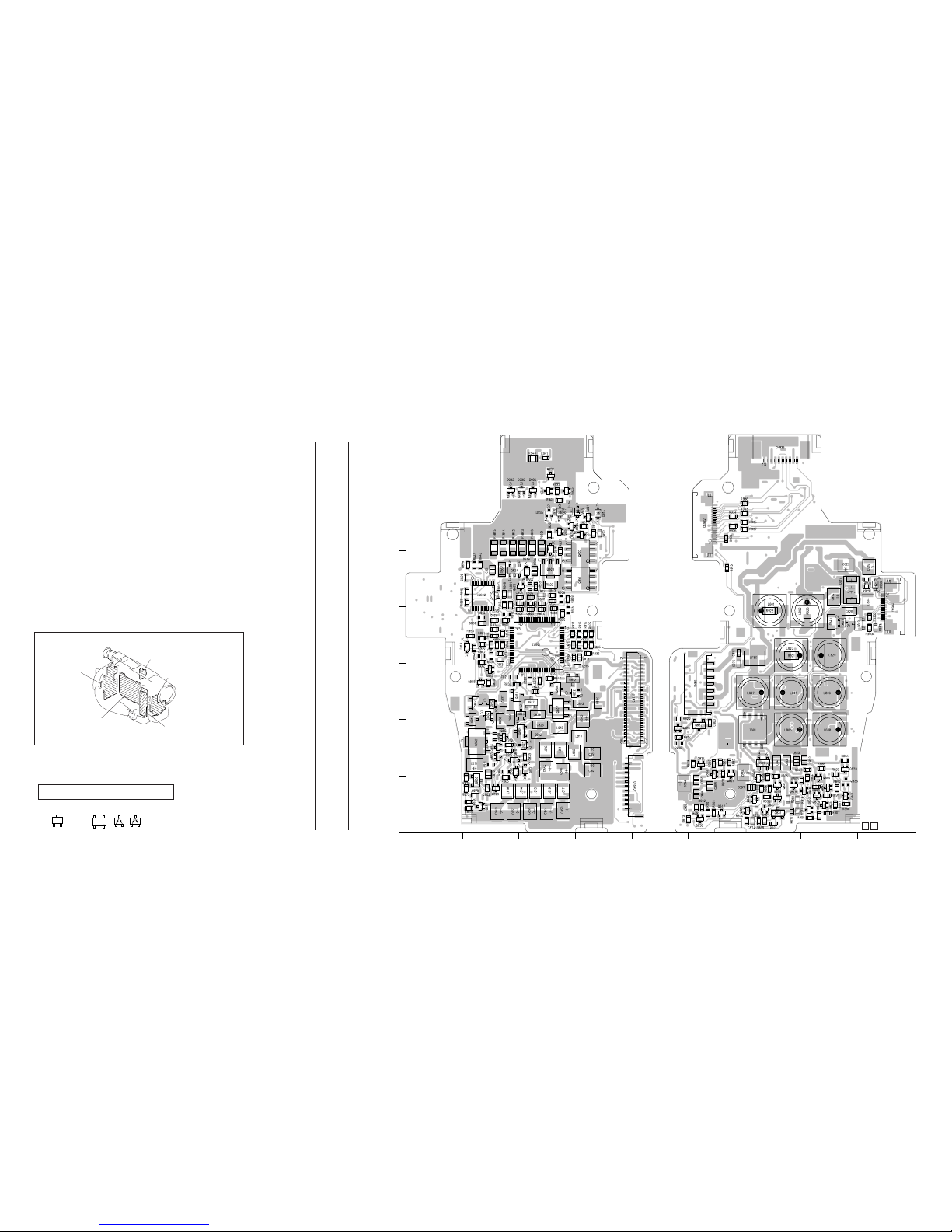
CCD-TRV3E/TRV13E/TRV23E/TRV45E/TRV55E/TRV65E/
TRV69E/TRV75/TRV75PK/TRV715
4-108 4-109
4-110
POWER
DD-105
DD-105 (POWER) PRINTED WIRING BOARD
– Ref No. DD-105 BOARD: 2,000 series –
DD-105 BOARD
C801 E-3
C802 E-3
C803 D-3
C804 E-3
C805 E-3
C806 E-3
C807 E-2
C808 E-3
C809 D-2
C810 D-3
C811 D-2
C812 D-4
C813 D-2
C814 E-8
C815 C-4
C816 E-9
C817 E-8
C819 C-3
C820 C-3
C821 C-2
C822 E-8
C823 C-4
C824 C-2
C825 B-3
C826 D-8
C827 E-2
C828 E-2
C829 E-2
C830 D-2
C831 E-2
C832 B-3
C833 B-3
C834 C-4
C836 B-2
C837 C-2
C838 C-3
C840 D-8
C841 B-4
C843 C-4
C844 A-3
C846 B-3
C847 B-7
C848 B-7
C849 A-2
C850 A-3
C851 B-4
C852 B-8
C853 B-7
C854 B-3
C855 A-3
C856 E-3
C857 A-2
C860 A-6
C861 A-7
C862 A-2
C863 B-6
C864 A-5
C866 A-6
C867 A-7
C868 B-6
C869 A-6
C871 B-2
C872 F-4
C873 A-2
C874 A-7
C875 B-2
C876 C-6
C877 D-6
C885 A-6
CN801 C-6
CN931 C-5
CN932 F-6
CN933 A-4
CN934 D-9
CN935 G-7
D801 B-3
D802 C-3
D803 C-2
D804 C-2
D805 C-3
D806 B-2
D807 D-8
D809 B-7
D810 B-2
D812 B-3
D813 F-4
D814 F-4
D815 F-3
D816 E-3
D817 F-3
D818 D-2
D819 E-3
D838 E-9
D932 G-2
D933 F-4
D934 G-3
D935 F-3
D936 G-3
FB931 D-9
FB932 E-9
FB933 D-9
FB934 D-9
IC801 D-3
IC802 E-2
R823 D-7
R824 D-2
R825 D-4
R826 D-4
R827 E-3
R828 F-3
R829 D-2
R830 D-2
R831 F-4
R832 D-4
R833 D-2
R834 D-2
R835 D-4
R836 D-4
R837 D-2
R838 D-3
R839 C-2
R840 C-3
R841 C-3
R842 E-2
R843 C-2
R849 E-2
R850 E-2
R852 D-2
R853 D-2
R854 D-2
R854 D-2
R859 E-3
R864 E-3
R865 A-2
R866 B-2
R867 E-2
R868 A-2
R870 A-7
R871 A-7
R872 B-6
R873 A-5
R874 B-5
R875 A-2
R876 B-5
R877 A-7
R878 A-2
R879 B-6
R880 B-6
R881 B-6
R882 B-6
R883 A-8
R884 B-8
R885 B-7
R887 B-8
R888 B-8
R889 A-7
R890 A-7
R891 A-8
R892 A-8
R893 B-8
R894 A-7
R895 A-6
R896 A-8
R897 A-8
R898 A-7
R899 A-7
R900 A-6
R901 A-6
R902 A-6
R903 A-8
R904 A-8
R905 A-8
R906 A-8
R907 A-8
R908 B-2
R910 B-2
R911 B-2
R912 B-2
R913 E-6
R914 D-2
R915 E-2
R916 A-7
R917 A-7
R918 A-2
R919 A-7
R920 A-7
R924 C-5
R932 G-3
R933 F-7
R934 F-6
R935 F-7
R936 F-6
R937 F-7
R938 F-7
R939 F-6
R940 F-3
R941 G-3
R942 E-9
R943 G-3
T801 B-7
L801 D-7
L802 D-7
L803 D-8
L804 E-9
L805 B-7
L806 C-8
L807 C-7
L808 B-8
L809 C-7
L810 B-4
L811 B-3
L812 B-3
L813 B-3
L814 A-3
L815 A-3
L816 B-3
L817 A-3
L818 A-2
L819 A-3
L820 D-8
LF801 D-7
PS801 F-3
PS802 F-2
PS803 F-3
PS804 F-2
PS805 F-2
PS806 F-3
Q801 F-4
Q802 E-4
Q803 E-3
Q804 F-3
Q805 F-3
Q806 C-2
Q807 C-3
Q808 C-3
Q809 B-3
Q810 C-2
Q812 C-3
Q813 C-2
Q814 C-2
Q815 C-2
Q817 C-3
Q819 D-8
Q820 E-3
Q823 A-2
Q824 E-2
Q826 A-7
Q827 A-2
Q828 B-5
Q829 B-6
Q830 B-6
Q831 A-7
Q832 B-6
Q833 A-2
Q834 B-6
Q835 A-8
Q836 A-8
Q837 A-7
Q838 A-8
Q839 B-8
Q840 A-8
Q841 A-7
Q842 A-7
Q843 A-7
Q844 A-8
Q845 A-8
Q846 A-7
Q847 A-6
Q848 A-8
Q849 A-7
Q850 A-8
Q851 E-4
Q852 B-2
Q853 B-2
Q854 B-2
Q855 B-2
Q856 A-6
Q932 G-3
Q933 G-3
Q934 G-3
R801 E-2
R802 E-3
R803 E-3
R804 D-3
R805 D-3
R807 E-3
R808 E-2
R808 E-3
R809 D-3
R810 E-2
R811 D-2
R812 D-2
R813 F-4
R814 D-4
R815 D-3
R816 D-4
R817 D-3
R818 D-2
R819 D-2
R820 D-3
R821 D-2
R822 E-3
R822 D-7
R822 D-8
• For Printed Wiring Boards.
• This board is four-layer print board. However, the patterns of
layers 2 to 3 have not been included in the diagram.
• Chip transistor Chip diode
There are few cases that the part isn't mounted in this model is
printed on this diagram.
Q
C
BE
43
21
D
123456789
A
B
C
D
E
F
G
09
DD-105 BOARD (SIDE B) DD-105 BOARD (SIDE A)
1-668-929-
12 22
1
2
3
21
3
21
CCD-TRV3E/TRV13E/TRV23E/TRV45E/TRV55E/TRV65E/
TRV69E/TRV75/TRV75PK/TRV715
CD-197 (2.5 INCH LCD MODEL)
CD-198 (3 INCH/3.5 INCH LCD MODEL)
(CCD IMAGER)
PJ-83 (2.5 INCH LCD MODEL)
PJ-84 (3 INCH/3.5 INCH LCD MODEL)
(AV IN/OUT)
MA-331 (2.5 INCH LCD MODEL)
MA-312 (3 INCH/3.5 INCH LCD MODEL)
(STEREO MIC, LASER LINK)
CF-50 (2.5 INCH LCD MODEL)
CF-51 (3 INCH/3.5 INCH LCD MODEL)
(CONTROL)
DD-105
(POWER)
Page 86
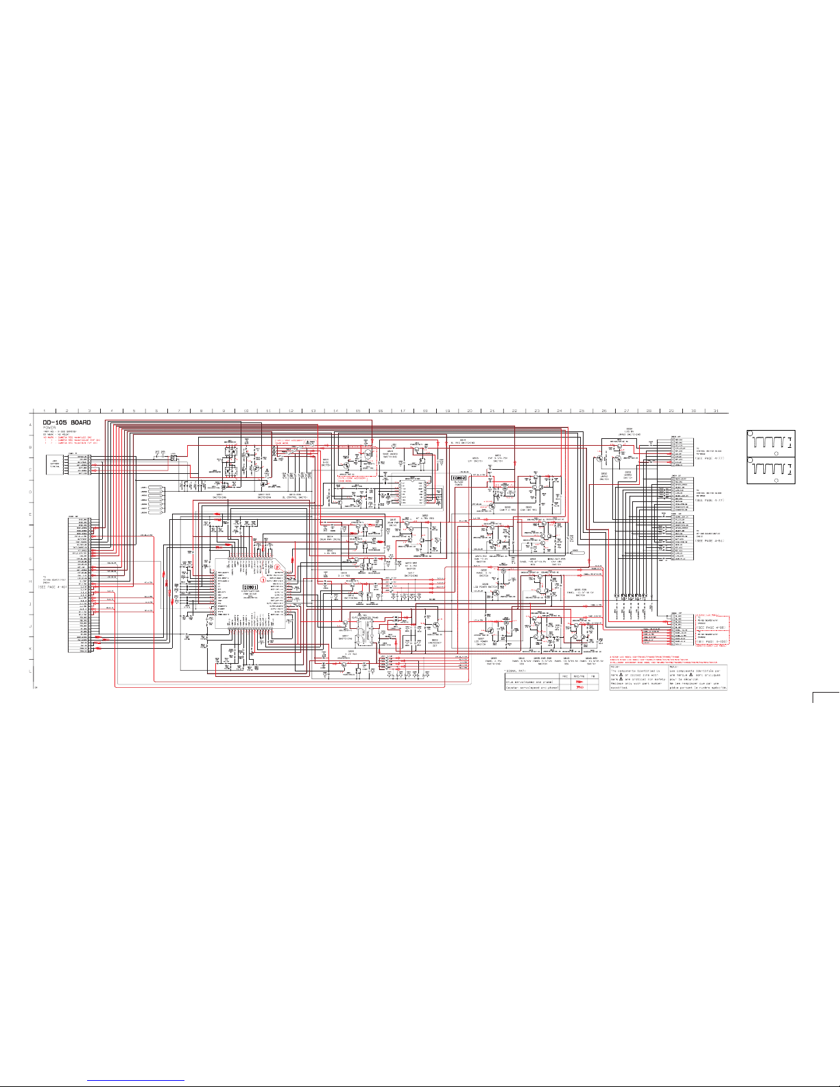
CCD-TRV3E/TRV13E/TRV23E/TRV45E/TRV55E/TRV65E/
TRV69E/TRV75/TRV75PK/TRV715
4-111 4-112
4-113
4-114E
POWER
DD-105
DD-105 BOARD
CAMERA REC
1
2
IC801 4
507 kHz
0.76Vp-p
IC801 64
506 kHz
0.76Vp-p
Page 87
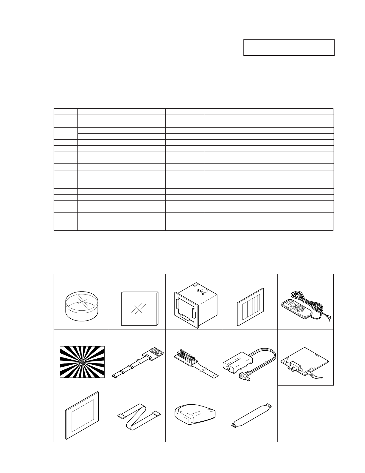
5-1
Parts Code
J-6080-058-A
J-6080-808-A
J-6080-818-A
J-6082-200-A
J-6020-250-A
J-6082-053-B
J-6080-875-A
J-6082-311-A
J-6082-382-A
J-6082-223-A
J-6082-312-A
J-6080-621-A
J-6082-357-A
J-6082-383-A
J-6082-188-A
Name
Filter for color temperature correction
(C14)
ND filter 1.0
ND filter 0.3
Pattern box PTB-450
Color chart for pattern box
Adjusting remote commander
(RM-95-remodeled partly) (Note 1)
Siemens star
Multi CPC jig
CPC-7 jig
Power code (Note 2)
AFM DEV jig
Clear chart
Extension cable (16P, 0.5 mm)
IR receiver jig
Extension cable (48P, 0.8 mm)
Ref. No.
J-1
J-2
J-3
J-4
J-5
J-6
J-7
J-8
J-9
J-10
J-11
J-12
J-13
J-14
Note 1: If the micro processor IC in the adjusting remote
commander is not the new micro processor (UPD7503GC56-12), the pages cannot be switched. In this case, replace
with the new micro processor (8-759-148-35).
SECTION 5
ADJUSTMENTS
Refer to page 3 as Table for distinction
functions of models and classification
5-1. CAMERA SECTION ADJUSTMENTS
1-1. PREPARATIONS BEFORE ADJUSTMENT
(CAMERA SECTION)
1-1-1. List of Service Tools
• Oscilloscope
• Adjusting driver
Usage
Auto white balance adjustment/check
White balance adjustment/check
White balance check
White balance check
For checking the flange back
For adjusting LCD block
For adjusting the video section
For connecting the battery terminal and DC power supply
For adjusting the deviation
For extension between the CD-197/198 board (CN401) and
VC-195 board (CN501)
For adjusting the IR transmitter
For extension between the DD-105 board (CN931) and
VC-195 board (CN914)
• Color monitor
• Regulated power supply
• Vectorscope
• Digital voltmeter
Note 2: Connect the adjusting remote commander to the LANC
jack, and set the HOLD switch to the “ADJ” side , or press
the battery switch of the battery terminal using adhesive
tape, etc.
Fig. 5-1-1.
J-1 J-2
J-3
J-4 J-5
J-7J-6 J-8 J-9 J-10
J-11 J-12 J-13 J-14
CCD-TRV3E/TRV13E/TRV23E/TRV45E/TR V55E/TRV65E/
TRV69E/TRV75/TR V75PK/TR V715
Page 88
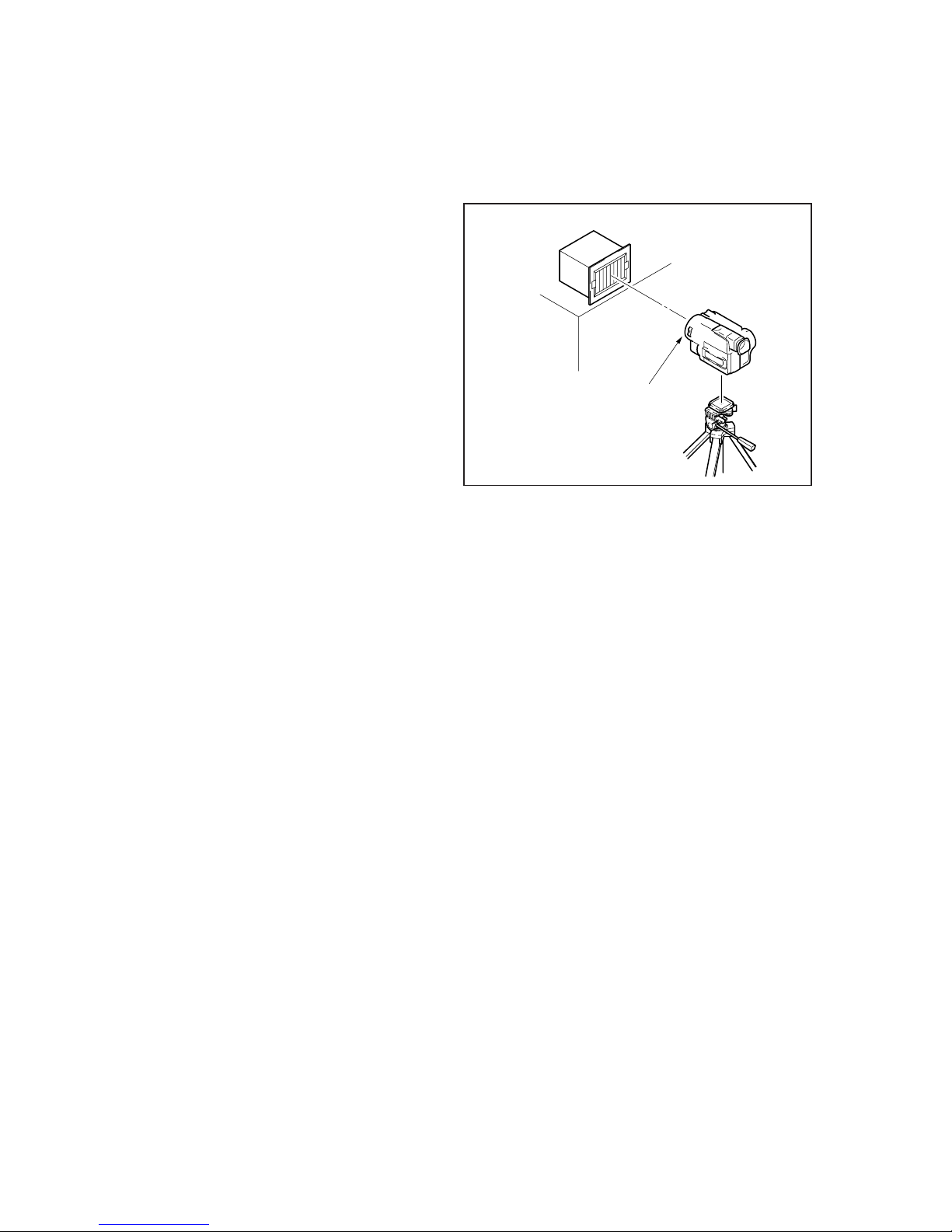
5-2
1-1-2. Preparations
Note 1: For details of how remove the cabinet and boards, refer to
“2. DISASSEMBLY”.
Note 2: When performing only the adjustments, the lens block and
boards need not be disassembled.
1) Connect the equipment for adjustments according to Fig. 5-1-3,
4.
2) By setting the “Forced Camera Power ON mode”, the camera
power can be turned ON even if the front panel b lock (MA-312/
331 board, power switch, microphone unit) has been removed.
When removing the front panel block disconnect the following
connector.
1. VC-195 board CN903 (23P 0.5mm)
3) The intelligent accessory shoe (Intelligent accessory shoe model)
or video light (Video light model) need not be assembled. If
removing it. disconnect the following connector.
1. VC-195 board CN909 (10P, 0.5mm)
Note 3: As removing the cabinet (R) (removing the VC-195 board
CN911) means removing the lithium 3V power supply
(CF-50/51 board) , data such as date, time, user-set menus
will be lost. After completing adjustments, reset these data.
If the cabinet (R) has been removed, the self-diagnosis
data, data on history of use (total drum rotation time etc. )
will be lost. Before removing, note down the self-diagnosis
data and data on the history use. (Refer to the “Service
Mode” of “VIDEO SECTION ADJUSTMENT” for the
data on the history use.)
Note 4: Setting the “Forced Camera Power ON” Mode
1)Select page: 0, address: 01, and set data: 01.
2)Select page: D, address: 10, set data: 01, and press the
PAUSE button of the adjusting remote commander.
The above procedure will enable the camera power to
be turned on with the front panel block removed. After
completing adjustments, be sure to exit the “Forced
Camera Power ON Mode”.
Note 5: Exiting the “Forced Camera Power ON” Mode
1)Select page: 0, address: 01, and set data: 01.
2)Select page: D, address: 10, set data: 00, and press the
PAUSE button of the adjusting remote commander.
3)Select page: 0, address: 01, and set data: 00.
Fig. 5-1-2.
Pattern box
1.5m
Front of lens
Page 89
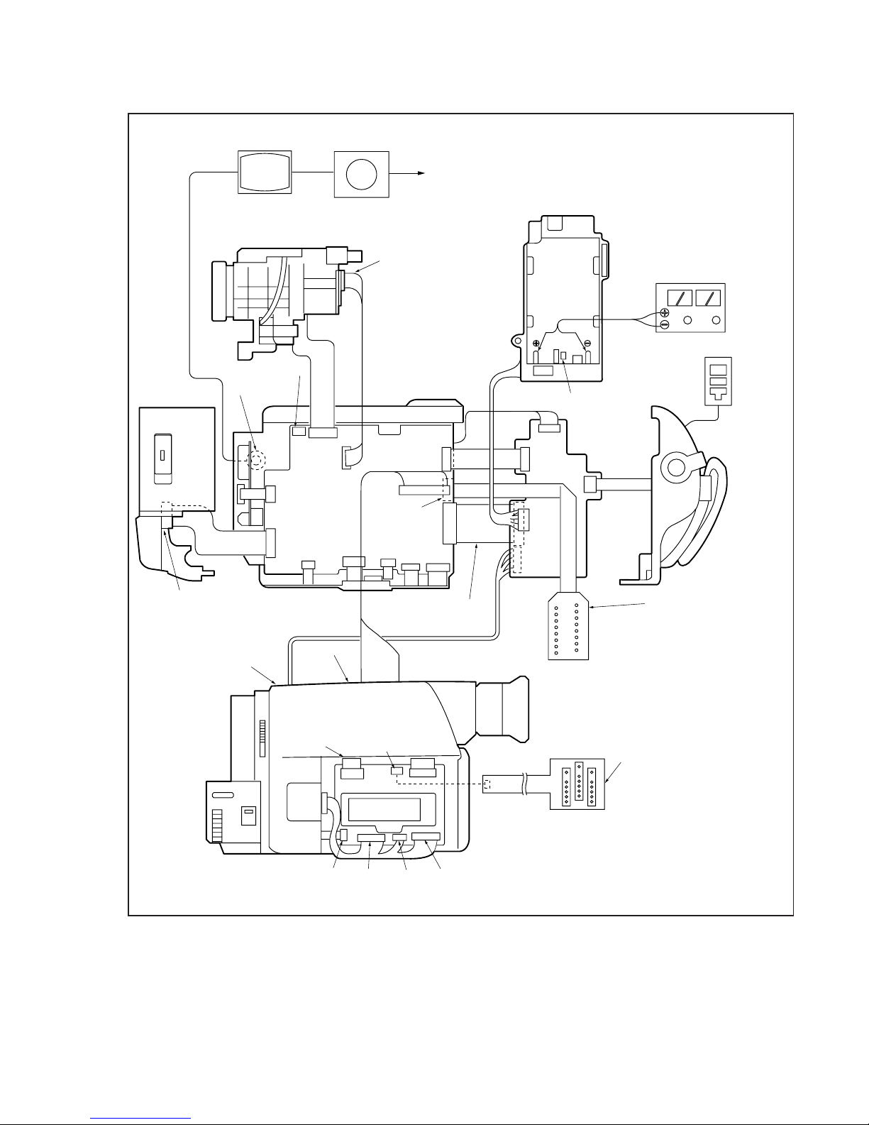
5-3
2.5 INCH LCD MODEL
Fig. 5-1-3.
Color monitor Vector scope
Terminated at 75
Ω
Lens block
CD-197 board
CN401
Extension cable(16P)
(J-6082-357-A)
Need not connected
VIDEO terminal
CN909
CN551
CN902
CN903
CN901
CN001
CN905
CN906
CN908
CN914
CN910
CN911
CN912
Battery switch
MA-331 board CN303
Extension cable(48P)
(J-6082-188-A)
CF-50
board
CN001
PD-92 board
CN580
PD-92 board
CN5701
CN5501
CN5001
CN5805
CN5802
CN5803
CN5804
Multi CPC jig
(J-6082-311-A)
Must be connected when
performing the LCD system
adjustments.
CPC-7 jig
(J-6082-382-A)
Must be connected when
performing the VIDEO system.
CN935
CN932
CN934
CN801
CN931
CN933
DD-105
board
LANC
jack
Adjusting
remote
commande
r
Regulaterd power supply
(8.4
±
0.1 Vdc)
Battery
terminal
(Note 2)
VC-195
board
CN501
Note 1 :2.5” LCD model : CCD-TRV3E/TRV13E/TRV23E/
TRV65E/TRV69E
Note 2 :Connect the adjusting remote commander to the LANC
jack, and set the HOLD switch to the “ADJ” side, or
press the battery switch of the battery terminal using
adhesive tape, etc. or use the AC power adaptor.
Page 90
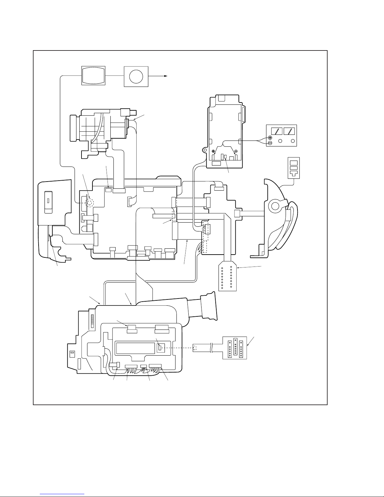
5-4
3/3.5 INCH LCD MODEL
Fig. 5-1-4.
Color monitor Vector scope
Terminated at 75
Ω
Lens block
CD-198 board
CN401
Extension cable(16P)
(J-6082-357-A)
Need not connected
VIDEO terminal
CN909
CN551
CN902
CN903
CN901
CN001
CN905
CN906
CN908
CN914
CN910
CN911
CN912
MA-312 board
CN303
Extension cable(48P)
(J-6082-188-A)
CF-51
board
CN001
PD-93 board
CN580
PD-93 board
CN4701
CN4501
CN4601
CN4805
CN4802 CN4803
CN4804
Multi CPC jig
(J-6082-311-A)
Must be connected when
performing the LCD system.
CPC-7 jig
(J-6082-382-A)
Must be connected when
performing the VIDEO system.
CN935
CN932
CN934
CN801
CN931
CN933
DD-105
board
LANC
jack
Adjusting
remote
commande
r
Regulaterd power supply
(8.4
±
0.1 Vdc)
Battery
terminal
(Note 2)
CN501
VC-195
board
Battery switch
Note 1 :3” LCD model : CCD-TRV75/TRV75PK/TRV715
3.5”LCD MODEL ; CCD-TRV45E/TRV55E
Note 2 :Connect the adjusting remote commander to the LANC
jack, and set the HOLD switch to the “ADJ” side , or
press the battery switch of the battery terminal using
adhesive tape, etc. or use the AC power adaptor.
Page 91
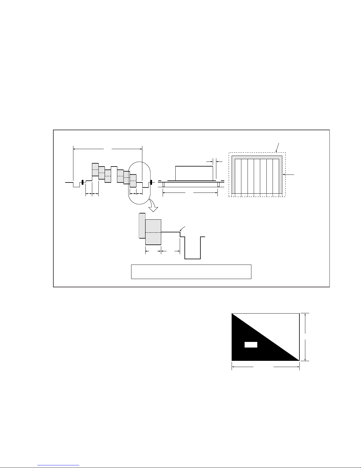
5-5
1-1-3.Precaution
1. Setting the Switch
Unless otherwise specified, set the switches as follows and perform
adjustments without loading cassette.
1. POWER switch (MA-312/331 board) ....................CAMERA
2. NIGHT SHOT switch (Lens Block)................................ OFF
(Night shot model)
3. DEMO MODE (Menu display) ....................................... OFF
4. DIGITAL ZOOM (Menu display)................................... OFF
5. STEADY SHOT (Menu display) .................................... OFF
6. DISPLAY (Menu display) ................................. V-OUT/LCD
7. FOCUS switch (MF-8500/MR-8500) ................... MANUAL
(Manual Focus model)
8. PROGRAM AE (CF-50/51 board) ..................................Auto
9. BACK LIGHT (CF-50/51 board) .................................... OFF
10. PICTURE EFECT (CF-50/51 board) .............................. OFF
11. 16 : 9 WIDE (Menu display)........................................... OFF
2. Adjusting Procedure
Adjust in the given order.
Fig. 5-1-5.
3. Subject
1) Color bar chart (Standard picture frame)
Adjust the picture frame as shown in Fig. 5-1-5. if adjustments
are performed using the color bar chart.
(Standard picture frame)
2) White pattern (Standard picture frame)
Remove the color bar chart from the pattern box, and insert a
clear chart in its place. (Do not perform zoom operations during
this time.)
3) Chart for flange back adjustment
Combine a white A0 size (1189 mm x 841 mm) paper to a black
one, and make the chart shown in Fig. 5-1-6.
Fig. 5-1-6.
Note : Use the non-reflecting and non-glazing vellum paper
whose size is more than A0, and make the boundary
between white and black to be smoothly flat.
Color bar chart standard picture trame
H
AB
A=B
B
A
0
±
0.1 msec
V
Enlargement
Difference in level
AB
Electronic beam
scanning frame
CRT picture fram
e
Fig. b. (TV monitor picture)
Yellow
Cyan
Green
White
Magenta
Red
Blue
Yellow
Cyan
Green
White
Magenta
Red
Blue
Fig. a. (Video output terminal
output wavefom)
Adjust the camera zoom and direction to obtain the output wavefom
shown in Fig. a and the TV monitor display shown in Fig. b.
841 mm
1189 mm
White
Black
Page 92
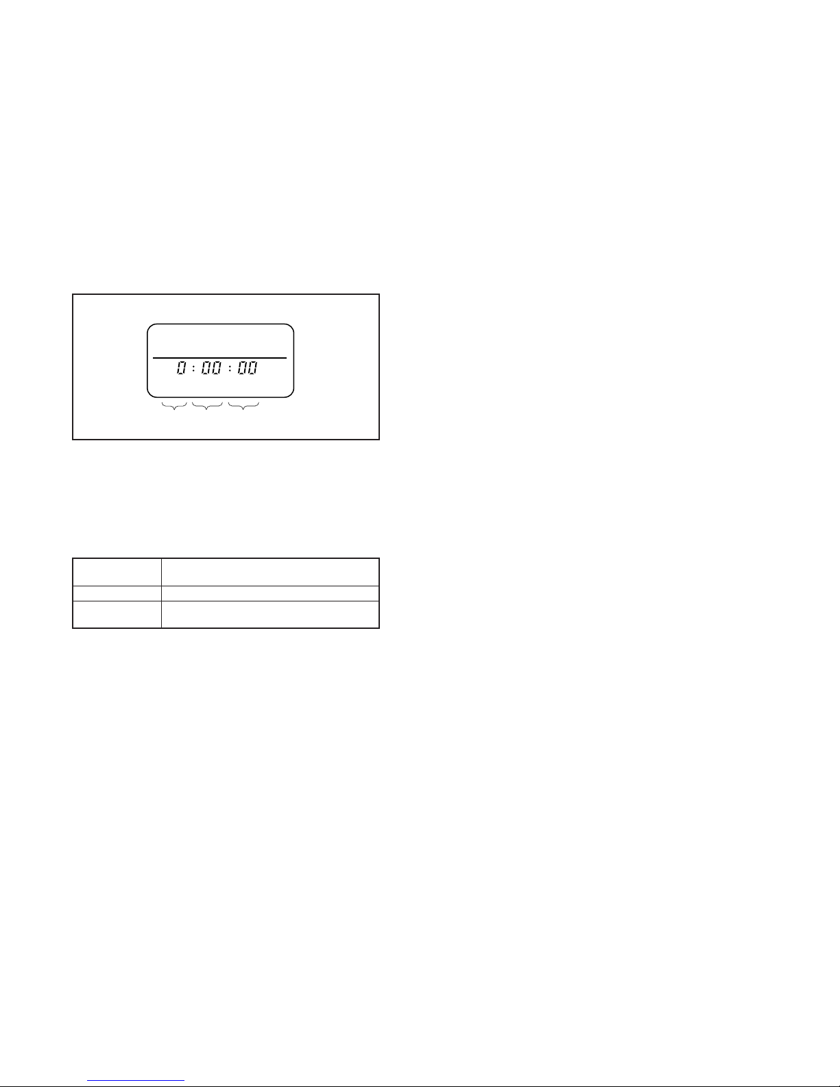
5-6
1-1-4. Adjusting Remote Commander
The adjusting remote commander is used for changing the
calculation coefficient in signal processing, EVR data, etc. The
adjusting remote commander performs bi-directional
communication with the unit using the remote commander signal
line (LANC). The resultant data of this bi-directional communication
is written in the non-volatile memory.
1. Using the adjusting remote commander
1) Connect the adjusting remote commander to the LANC terminal.
2) Adjust the HOLD switch of the adjusting remote commander to
“HOLD” (SERVICE position).
If it has been properly connected, the LCD on the adjusting remote
commander will display as shown in Fig. 5-1-7.
Fig. 5-1-7.
3) Operate the adjusting remote commander as follows.
• Changing the page
The page increases when the EDIT SEARCH+ button is
pressed, and decreases when the EDIT SEARCH– button is
pressed. There are altogether 16 pages, from 0 to F.
Table 5-1-1.
• Changing the address
The address increases when the FF ()) button is pressed,
and decreases when the REW (0) button is pressed. There
are altogether 256 addresses, from 00 to FF.
• Changing the data (Data setting)
The data increases when the PLAY (() button is pressed,
and decreases when the STOP (p) button is pressed.
There are altogether 256 data, from 00 to FF.
• Writing the adjustment data
The PAUSE button must be pressed to write the adjustment
data (D, E, F page) in the nonvolatile memory.
(The new adjustment data will not be recorded in the nonv olatile
memory if this step is not performed.)
4) Select page: 0, address: 01, and set the data to 01, and enables
Page D and E, F to be adjusted.
5) After completing all adjustments, set data: 00 to page: 0, address:
01 and turn off the main power supply (8.4V) once.
2. Precautions upon using the adjusting remote
commander
Mishandling of the adjusting remote commander may erase the
correct adjustment data at times. T o prev ent this, it is recommended
that all adjustment data be noted down before beginning adjustments
and new adjustment data after each adjustment.
Page Data
Address
0123456789ABCDEF
0 123456789A b c d E F
0123456789101112131415
Hexadecimal
notation
LCD Display
Decimal notation
conversion value
Page 93
5-7
Hexadecimal notation-Decimal notation
Note: ( ) indicate the adjusting remote commander display.
(Example) In the case that the DDS display and the adjusting remote commander display are BD (bd).
As the upper digit of the hexadecimal notation is B (b), and the lower digit is D (d), the intersection “189" of the 1
and 2 in the above table is the decimal notation to be calculated.
The lower digits of the
hexadecimal notation
0123456789ABCDEF
(
A)(b)(c)(d)(E)(F)
The upper digits of the
hexadecimal notation
0
1
2
3
4
5
6
7
8
9
A (
A)
B (
b)
C (
c)
D (
d)
E (
E)
F (
F)
0123456789101112131415
16 17 18 19 20 21 22 23 24 25 26 27 28 29 30 31
32 33 34 35 36 37 38 39 40 41 42 43 44 45 46 47
48 49 50 51 52 53 54 55 56 57 58 59 60 61 62 63
64 65 66 67 68 69 70 71 72 73 74 75 76 77 78 79
80 81 82 83 84 85 86 87 88 89 90 91 92 93 94 95
96 97 98 99 100 101 102 103 104 105 106 107 108 109 110 111
112 113 114 115 116 117 118 119 120 121 122 123 124 125 126 127
128 129 130 131 132 133 134 135 136 137 138 139 140 141 142 143
144 145 146 147 148 149 150 151 152 153 154 155 156 157 158 159
160 161 162 163 164 165 166 167 168 169 170 171 172 173 174 175
176 177 178 179 180 181 182 183 184 185 186 187 188 189 190 191
192 193 194 195 196 197 198 199 200 201 202 203 204 205 206 207
208 209 210 211 212 213 214 215 216 217 218 219 220 221 222 223
224 225 226 227 228 229 230 231 232 233 234 235 236 237 238 239
240 241 242 243 244 245 246 247 248 249 250 251 252 253 254 255
n
1n
1-1-5. Data Processing
The calculation of the DDS display and the adjusting remote
commander display data (hexadecimal notation) are required for
obtaining the adjustment data of some adjustment items. In this case,
after converting the hexadecimal notation to decimal notation,
calculate and convert the r esult to hexadecimal notation, and use it
as the adjustment data. Table 5-1-2. indicates the hexadecimal
notation-the decimal notation calculation table.
Table 5-1-2.
2
Page 94
5-8
1-2. INITIALIZATION OF D, E, F PAGE DATA
1. Initializing the D,E,F Page Data
Note 1: If “Initializing the D, E, F Page Data” is performed,
all data of the D page, E page and F page will be
initialized. (It is impossible to initialize a single
page.)
Note 2: If the D,E,F page data has been initialized, “Modification
of D, E, F Page Data” and all adjustments need to be
performed again.
Note 3: < > : NTSC model (CCD-TRV75/TRV75PK/TRV715)
[ ] : PAL model (CCD-TRV3E/TRV13E/TRV23E/
TRV45E/TRV55E/TRV65E/TRV69E)
Initializing Method:
1) Select page: 0, address: 01, and set data: 01.
2) Select page: 2, address: 00, and set data: 55 <NTSC> or
data : 51 [PAL].
3) Select page: 2, address: 01, set data: 55<NTSC> or data : 51
[PAL], and press the PAUSE button of the adjusting remote
commander.
4) Select page: 2, address: 02, and check that the data is 01.
5) Select page: 3, address: 00, and set data: 29.
6) Select page: 3, address: 01, set data: 29, and press the PAUSE
button of the adjusting remote commander.
7) Select page: 0, address: 01, and set data: 00.
8) Perform “Modification of D,E,F Page Data”.
Adjusting page D
Adjusting Address 00 to 6F
Adjusting page F
Adjusting Address 00 to FF
Adjusting page E
Adjusting Address 00 to FF
2. Modification of D, E, F Page Data
If the D, E, F page data has been initialized, change the data of the
“Fixed data-2” address shown in the following tables by manual
input.
Modifying Method:
1) Before changing the data, select page: 0, address: 01, and set
data: 01.
2) New data for changing are not shown in the tables because they
are different in destination. When changing the data, copy the
data built in the same model.
Note : If copy the data built in the different model, the camcorder
may not operate.
3) When changing the data, press the PA USE b utton of the adjusting
remote commander each time when setting new data to write the
data in the non-volatile memory.
4) Check that the data of adjustment addresses is the initial value.
If not, change the data to the inital value.
5) After compleating “Modification of D , E, F Paga Data” select
page: 0, address: 01, and set data: 00. Also perform all
adjustments.
Page 95
5-9
Address Initial Value Remark
NTSC PA L
00 to 0F
10 00 00 Fixed data-1
11 00 00 (Initialized data)
12 00 00
13 Fixed data-2
14 (Modified data, copy the data
15 built in the same model.)
16
17
18
19
1A
1B
1C
1D
1E
1F
20
21
22
23
24
25
26
27
28
29
2A Fixed data-1
2B (Initialized data)
2C
2D
2E Fixed data-2
2F
30 88 88 Battery end adj.
31 8D 8D
32 A8 A8
33 BD BD
34 C8 C8
35 Fixed data-2
36 (Modified data, copy the data
37 built in the same model.)
38
39
3A
3B
3C
3D
3E
3F
40
41
42
43
44
45
46
47
48
49
4A
Address Initial V alue Remark
NTSC PAL
4B Fixed data-1
4C (Initialized data)
4D
4E
4F
50 Fixed data-2
51 (Modified data, copy the data
52 built in the same model.)
53
54
55
56
57
58
59
5A
5B
5C
5D
5E
5F
60 Fixed data-1
61 (Initialized data)
62
63
64
65
66
67
68
69
6A
6B
6C
6D
6E
6F
3. D Page Table
Note1 :
Fixed data-1 : Initialized data.
(Refer to “1. Initializing the D,E,F Page Data”.)
Fixed data-2 : Modified data.
(Refer to “2. Modification of D, E, F Pa ge Data”).
Page 96
5-10
4. F Page table
Note 1:
Fixed data-1 : Initialized data.
( Refer to “1. Initializing the D,E,F Page Data”.)
Fixed data-2 : Modified data.
(Refer to “2. Modification of D, E, F Page Data”).
Note 2: There are three models classified by CCD imager types as
shown below , and the initial value of adjustment is dif ferent
according to the model.
NTSC 760H model : CCD-TRV75/TRV75PK/TRV715
PAL 760H model : CCD-TR V45E/TRV55E/TRV65E/TRV69E
PAL 510H model : CCD-TRV3E/TRV13E/TRV23E
Note 3 :There are three models classified by VTR formats as shown
below, and the initial value of adjustment is different
according to the model.
NTSC Hi8 model : CCD-TRV75/TRV75PK/TRV715
PAL Hi8 model : CCD-TRV65E/TRV69E
PAL Standard8 model : CCD-TRV3E/TRV13E/TRV23E/
TRV45E/TRV55E
Address Initial Value Remark
NTSC PAL
Address Initial Value Remark
NTSC PA L
00 to 0F
10 00 00 Emergency memory address
11 00 00
12 00 00
13 00 00
14 00 00
15 00 00
16 00 00
17 00 00
18 00 00
19 00 00
1A 00 00
1B 00 00
1C Fixed data-2
1D
1E
1F
20
21 D2 <D2>,
G-CAM flip adj.
[D0]
< > : CCD-TRV3E/TRV13E/TRV23E
[ ] : CCD-TRV45E/TRV55E/TRV65E/TRV69E
22 Fixed data-2
23
24 Fixed data-1
25 (Color reproduction adj.)
26 Fixed data-2
27
28
29 Fixed data-1
2A
2B Fixed data-2
2C A0 A0 28MHz origin osc. adj.
2D Fixed data-2
2E Fixed data-1
2F 80 80 Hall adj.
30 80 80
31 08 18/08 Max gain adj.
Note 2 : 510H model/ 760H model
32 Fixed data-1
33
34 1B 1B Color reproduction adj.
35 Fixed data-1
36 42 42 Color reproduction adj.
37 Fixed data-1
38
39
3A 89 89 Auto white balance adj.
3B 59 59
3C 38 38 IRIS IN/OUT adj.
3D 41 41
3E 25 25 Flange back adj.
3F 00 00
40 19 19
41 00 00
42 35 35
43 52 52 Angular velocity sensor
44 52 52 sensitivity adj.
45 7A 7A 1.5MHz deviation adj.
46 8D 8D 1.7MHz deviation adj.
47 7A 7A BPF f0 adj.
48 Fixed data-1
49 6B 6B Y OUT level adj.
4A 40 40 AFC f0 adj.
4B 9A 9A C OUT level adj.
4C Fixed data-1
4D 7B 7B Filter f0 adj.
4E 60 60 RP filter f0 adj.
4F Fixed data-1
50
51
52
53 40 40 REC Y current adj.
54 40 40 Addresses 57 to 5A are fixed
55 5F 40 data addresses.
56 5F 40 Note 3 : Hi8 model/ Standard8 model
57 A0 A1/80
58 80 95/80
59 90 A1/80
5A 80 95/80
5B 50 50 REC L level adj.
5C 50 50 Addresses 63 to 64 are fixed
5D 43 50 data addresses.
5E 43 50
5F 66 66
60 66 66
61 67 66
62 67 66
63 7C 7A/80 Note 3 : Hi8 model/ Standard8 model
64 78 7A/80
65 80 80 REC C current adj.
66 41 41 IR video deviation Adj.
67 33 33 IR audio deviation Adj.
68 C7 C7 IR video carrier freq. Adj.
69 3C 3C CAP FG offset adj.
6A Fixed data-2
6B Fixed data-1
6C
6D
6E
6F
70 3B 3B AWB standard data input adj.
71 FF FF
72 56 56
73 7D 7D
74 Fixed data-1
75
76 1B 1B Flange back adj.
77 54 54
78 25 25
79 80 80
7A 10 10
7B FF FF
Page 97
5-11
Address Initial Value Remark
NTSC PAL
Address Initial Value Remark
NTSC PA L
7C 0A 0A Switching position adj.
7D 00 00
7E 0A 0A
7F 00 00
80 Fixed data-2
81
82 Fixed data-1
83
84 Fixed data-2
85 Fixed data-1
86 Fixed data-2
87 Fixed data-1
88
89
8A
8B
8C
8D
8E Fixed data-2
8F Fixed data-1
90
91
92
93
94 Fixed data-2
95
96 Fixed data-1
97
98 Fixed data-2
99 Fixed data-1
9A Fixed data-2
9B Fixed data-1
9C Fixed data-2
9D Fixed data-1
9E Fixed data-2
9F Fixed data-1
A0 Fixed data-2
A1
A2
A3
A4
A5 Fixed data-1
A6 Fixed data-2
A7
A8
A9
AA Fixed data-1
AB
AC Fixed data-2
AD Fixed data-1
AE Fixed data-2
AF Fixed data-1
B0
B1
B2
B3
B4
B5
B6
B7
B8
B9
BA
BB
BC
BD
BE Fixed data-2
BF
C0 Fixed data-1
C1
C2
C3
C4
C5 Fixed data-2
C6 Fixed data-1
C7
C8 Fixed data-2
C9
CA Fixed data-1
CB
CC
CD
CE
CF
D0
D1
D2
D3
D4
D5
D6
D7
D8
D9 Fixed data-2
DA Fixed data-1
DB
DC Fixed data-2
DD Fixed data-1
DE
DF
E0
E1
E2
E3 Fixed data-2
E4
E5 Fixed data-1
E6 Fixed data-2
E7 Fixed data-1
E8
E9
EA
EB Fixed data-2
EC
ED Fixed data-1
EE
EF
F0
F1
F2 Fixed data-2
F3 Fixed data-1
F4
F5 FF FF Color reproduction adj.
F6 F6 F4
F7 Fixed data-1
F8
F9
FA
FB
FC
FD
FE
FF
Page 98
5-12
Address Initial Value Remark
NTSC PA L
Address Initial V alue Remark
NTSC PAL
38 Fixed data-2
39
3A
3B Fixed data-1
3C
3D
3E
3F
40
41
42
43
44
45
46
47
48
49
4A
4B
4C
4D
4E
4F Fixed data-2
50 Fixed data-1
51 Fixed data-2
52
53 Fixed data-1
54
55
56
57
58
59 Fixed data-2
5A
5B Fixed data-1
5C Fixed data-2
5D Fixed data-1
5E
5F
60 Fixed data-2
61
62
63
64
65
66
67
68 Fixed data-1
69
6A
6B Fixed data-2
6C
6D Fixed data-1
6E Fixed data-2
6F
70
71
72 Fixed data-1
73 Fixed data-2
74 Fixed data-1
75 Fixed data-2
76 to 99 Fixed data-1
5. E Page T able
Note 1:
Fixed data-1 :Initialized data.
( Refer to “1. Initializing the D,E,F Page Data”.)
Fixed data-2 :Modified data.
(Refer to “2. Modification of D, E, F Page Data”).
Note 2: See “1-5. LCD SYSTEM ADJUSTMENT”.
00 Fixed data-1
01
02
03
04
05
06
07
08
09
0A
0B
0C
0D
0E
0F
10
11
12
13
14 Fixed data-2
15 Fixed data-1
16
17
18
19
1A
1B
1C
1D
1E
1F
20
21
22
23
24
25
26
27
28
29
2A
2B Fixed data-2
2C
2D
2E
2F Fixed data-1
30
31
32
33
34
35
36
37
Page 99
5-13
Address Initial Value Remark
NTSC PA L
Address Initial Value Remark
NTSC PAL
D9 Note 2 Note2 Fixed data (NTSC model)
Color adj. (LCD) (PAL model)
DA Fixed data-1
DB Fixed data-2
DC Fixed data-1
DD
DE
DF
E0
E1
E2
E3
E4
E5
E6
E7
E8
E9
EA Fixed data-2
EB
EC Fixed data-1
ED
EE
EF Fixed data-2
F0 Fixed data-1
F1
F2
F3 Fixed data-2
F4 Fixed data-1
F5
F6
F7
F8
F9
FA
FB
FC to FF
9A Fixed data-2
9B Fixed data-1
9C Fixed data-2
9D Fixed data-1
9E
9F
A0 Fixed data-2
A1
A2
A3
A4 Fixed data-1
A5
A6
A7
A8
A9
AA
AB
AC
AD
AE
AF
B0
B1
B2
B3
B4
B5
B6
B7
B8
B9
BA
BB
BC Fixed data-2
BD
BE
BF Note2 Note2 Fixed data (NTSC model)
VCO adj. (LCD) (PAL model)
C0 Fixed data-2
C1
C2 Fixed data-1
C3
C4
C5
C6
C7 Fixed data-2
C8
C9
CA
CB
CC Fixed data-1
CD
CE
CF Note 2 Note2 Bright adj. (LCD)
D0 Note 2 Note2 Color adj. (LCD)
D1 Note 2 Note2 White balance adj. (LCD)
D2 Note 2 Note2 White balance adj. (LCD)
D3 Note 2 Note2 Contrast adj. (LCD)
D4 Note 2 Note2 D range adj. (LCD)
D5 Note 2 Note2 V-COM level adj. (LCD)
D6 Note 2 Note2 VCO adj. (LCD)
D7 Note 2 Note2 V-COM adj. (LCD)
D8 Fixed data-1
Page 100
5-14
1-3. CAMERA SYSTEM ADJUSTMENTS
Before perform the camera system adjustments, Check that the
specified value of “28MHz Origin Oscillation Adjustment”, “Y OUT
level Adjustment” and “C OUT level Adjustment” of “VIDEO
SYSTEM ADJUSTMENT” are satisfied.
1. G-CAM flip Adjustment
Set the color reproduction conditions to optimum.
Subject Color bar chart standard picture frame
Measurement Point Display data of page 1 of the adjusting
remote commander (Note 1)
Measuring Instrument
Adjustment Page F
Adjustment Address 21
Note 1. Displayed data of page 1 of the adjusting remote
commander.
1 :
XX : XX
n S2
n S1
Note 2. [ ] : Except CCD-TRV3E/TRV13E/TRV23E
< > : CCD-TRV3E/TRV13E/TRV23E
Adjusting method:
1) Select page: 0, address: 01, and set data: 01.
2) Select page: 0, address: 03, and set data: 16.
3) Select page: F, address: 21, set data: [D2] <D0>, and press the
PAUSE button of the adjusting remote commander.
4) Select page 1 of the adjusting remote commander, and compare
the higher 2 digits (S1) and lower 2 digits (S2) of the 4-degits
display data.
When S1<S2
Perform steps 5) onwards.
When S1 S2
Perform steps “Processing after Completing Adjustments”.
5) Select page: F, address: 21, set data: [52] <50>, and press the
PAUSE button of the adjusting remote commander.
Processing after Completing Adjustments
1) Select page: 0, address: 03, and set data: 00.
2) Select page: 0, address: 01, and set data: 00.
 Loading...