

Page 1

Intel Mini PCI Wireless Card Specification Revision 1.0c July 2, 2002
Intel Mini PCI Wireless Card
Specification
(Supplement to Mini PCI Specification)
Lonnie McAlister
Intel Confidential Page 1 of 13
Page 2

Intel Mini PCI Wireless Card Specification Revision 1.0c July 2, 2002
THIS SPECIFICATION IS PROVIDED "AS IS" WITH NO WARRANT IES WHATSOEVER,
INCLUDING ANY WARRANTY OF MERCHANTABILITY, NONINFRINGEMENT, FITNESS FOR
ANY PARTICULAR PURPOSE, OR ANY WARR ANT Y OTHERWISE ARISING OUT OF ANY
PROPOSAL, SPECIFICATION OR SAMPLE. Intel disclaims all liability, including liability for
infringement of any proprietary rights, relating to use of information in this specification. No license, express
or implied, by estoppel or otherwise, to any intellectual property rights is granted herein.
This document is an intermediate draft for comment only and is subject to change without notice. Readers
should not design products based on this document.
Copyright © Intel Corporation (appropriate year). *Third-party brands and names are the property of their
respective owners.
Intel Confidential Page 2 of 13
Page 3

Intel Mini PCI Wireless Card Specification Revision 1.0c July 2, 2002
Table of Contents
1. DOCUMENT REVISION HISTORY.................................................................................4
2. REFERENCES..............................................................................................................4
3. PURPOSE....................................................................................................................4
4. B
5. M
6. MINI PCI SYSTEM CONNECTOR PINS .......................................................................5
7. LED INDICATORS AND SWITCH..................................................................................7
8. MECHANICAL ............................................................................................................10
ACKGROUND OF THIS MINI PCI SPECIFICATION ADDENDUM..................................4
INI PCI V1.0 DEFINED FUNCTION-SPECIFIC CONNECTORS ..................................5
6.1 Sparks/Calexico Mini PCI Pino ut Dev iat ion to Sys tem Conn ec tor Pins :.....................6
6.1.1 LEDs....................................................................................................................6
6.2 Other Deviations on the Mini PCI edge connector ...................................................7
7.1 WLAN LINK Indicator ............................................................................................7
7.2 WLAN Activity Indicator.........................................................................................8
7.3 Radio Transmitter Disable Switch...........................................................................8
7.4 Spectrum Indication Control Signal.........................................................................9
7.5 Bluetooth Coexistence ........................................................................................10
8.1 PCB Card Design................................................................................................10
8.2 Antenna Connection............................................................................................11
Intel Confidential Page 3 of 13
Page 4

Intel Mini PCI Wireless Card Specification Revision 1.0c July 2, 2002
1. Document Revision History
Revision Date Comments
0.1 Dec 28, 2001 First draft
0.8 Jan. 08, 2002 Released to Engineering
0.85 Feb. 11, 2002
0.90 11 March 11,
2002
0.95 March 14, 2002 Updated Mini PCI edge connector
0.99 March 18, 2002 Draft release. Need Dual LED circuit
1.0 April 12, 2002 Updated LED reference circuit.
1.0b May 20, 2002 Updated edge connector pin-out for
• Updated for OEM customizations:
• Added antenna mechanical
tolerances for type 3A and type 3B
card.
•
Updated pinout table
Updated LED configuration (again)
deviations section. Simplified LED
function description.
implementation yet.
Updated H/W Kill switch implementation
Bluetooth co-existence
Updated manufacturing bevel design
requirements
2. References
This addendum is based upon the Mini PCI Specification, Revision 1.0, October 25th, 1999.
Additional information can be found in the PCI 2.2 specification.
3. Purpose
This document is intended for PC OEM custom ers designing for a wireles s Mini PCI solution the
opportunity to review Int el’s Calexico Mini PCI pin ou t connections, mechanical requirements, and
custom interfaces and be able to design their platform(s) to support the Calexico Mini PCI card.
4. Background of this Mini PCI Specification Addendum
The Mini PCI specification is an industry-standard specification whose intent is to provide
system/platform designers and card d esigner s with t he abili ty to us e a stan dards -based i nterf ace to
design to while stil l prov iding s ome f lexibilit y/options in system and car d designs. The or iginal Min i
PCI specification did achieve its goal but at the time only LAN and modem technologies were
envisioned for this form-factor. Since the release of the first Mini PCI specification, wireless
technology has appear ed in the market and is now appearing on Mini PCI cards, which intr oduces
unique challenges to both the s ystem and card m anufacturers. The purpos e of this document is to
define the “custom ” pinout configuration used by Calexico to ach ieve the proper perf ormance and
unique feature set that Intel is providing with this generation of wireless Mini PCI card.
Intel Confidential Page 4 of 13
Page 5

Intel Mini PCI Wireless Card Specification Revision 1.0c July 2, 2002
_
5. Mini PCI v1.0 Defined Function-Specific Connectors
The MPCI specific ation defines function-s pecific connector s on the MPCI card for Wired LAN and
Modem functionality.
• The function-specific LAN connector. This is a 14-pin connector.
• The function-specific Modem connector. This is a 2-pin connector.
After reviewing next generation board layouts as well as the customer drive for more and more
capability while dr i ving s maller form fac tors , the 1 4 pin I/O connector will no lo nger be supported on
Intel wireless Mini PCI cards going f orward. Intel will continue t o support the tw o-pin connec tor for
support of an AC’97 modem.
6. Mini PCI System Connector Pins
The Mini PCI edge connec tor pinout definition as described in the Mini PCI Speci fication, Revisio n
1.0, is shown below. T he Intel wireless Mini PCI card will com ply to this pinout for c ompatibility
purposes except for deviations as noted in this section.
Table 1: Mini PCI Card Type III System Connector Pinout
Pin Signal Pin Signal Pin Signal Pin Signal
1
KEY KEY 65
3
5
7
9
11
13
15
17
19
21
23
25
27
29
31
33
35
37
39
41
43
45
47
49
51
53
TIP
8PMJ-3
8PMJ-6
8PMJ-7
8PMJ-8
LED1_GRNP
LED1_GRNN
CHSGND
INTB#
3.3V
RESERVED
GROUND
CLK
GROUND
REQ#
3.3V
AD[31]
AD[29]
GROUND
AD[27]
AD[25]
RESERVED
C/BE[3]#
AD[23]
GROUND
AD[21]
AD[19]
2
4
6
8
10
12
14
16
18
20
22
24
26
28
30
32
34
36
38
40
42
44
46
48
50
52
54
RING
8PMJ-1
8PMJ-2
8PMJ-4
8PMJ-5
LED2_YELP
LED2_YELN
RESERVED
5V
INTA#
RESERVED
3.3VAUX
RST#
3.3V
GNT#
GROUND
PME#
RESERVED
AD[30]
3.3V
AD[28]
AD[26]
AD[24]
IDSEL
GROUND
AD[22]
AD[20]
63 3.3V 64
CLKRUN#
67
SERR#
69
GROUND
71
PERR#
73
C/BE[1]#
75
AD[14]
77
GROUND
79
AD[12]
81
AD[10]
83
GROUND
85
AD[08]
87
AD[07]
89
3.3V
91
AD[05]
93
RESERVED
95
AD[03]
97
5V
99
AD[01]
101
GROUND
103
AC_SYNC
105
AC_SDATA_IN
107
AC_BIT_CLK
109
AC_CODEC_ID1#
111
MOD_AUDIO_MON
113
AUDIO_GND
115
SYS_AUDIO_OUT
117
SYS
AUDIO_OUT
66
68
70
72
74
76
78
80
82
84
86
88
90
92
94
96
98
100
102
104
106
108
110
112
114
116
118
FRAME#
TRDY#
STOP#
3.3V
DEVSEL#
GROUND
AD[15]
AD[13]
AD[11]
GROUND
AD[09]
C/BE[0]#
3.3V
AD[06]
AD[04]
AD[02]
AD[00]
RESERVED_WIP
4
RESERVED_WIP
4
GROUND
M66EN
AC_SDATA_OUT
AC_CODEC_ID0#
AC_RESET#
RESERVED
GROUND
SYS_AUDIO_IN
SYS_AUDIO_IN
Intel Confidential Page 5 of 13
Page 6

Intel Mini PCI Wireless Card Specification Revision 1.0c July 2, 2002
A
A
GND GND
55
57
59
61
6.1 Sparks/Calexico Mini PCI Pinout Deviation to System Connector Pins:
6.1.1 LEDs
PIN Old Signal Name New Signal Name Signal Definition .
11 LED1_GRNP LED_WLAN_LINK
12 LED2_YELP LED_WLAN_ACT
13 LED1_GRNN
14 LED2_YELN
36 RESERVED
43 RESERVED
GROUND
AD[17]
C/BE[2]#
IRDY#
56
58
60
62
PAR
AD[18]
AD[16]
GROUND
HW_RadioXMIT_OFF
#
WLAN_Radio_State#
(spectrum
identification)
Channel_Clk
BT_priority
Channel_Data
11b_activity
119
AUDIO_GND
121
RESERVED
123
VCC5VA
Active-high LED drive signal provides an
indication of acc ess point ass ociation. This s ignal
will blink slowly every 3 seconds until association
occurs at which time it will be HIGH until
association is lost. During initia li za tio n or whi le t he
radios are in reset, the signal will be LOW.
Note: 0 ohm series res istor provides connection
to the Mini PCI edge connector
Active-high LED drive signal provides an
indication of data activity. This signal will blink
rapidly when data traffic is occurring. During
initialization, or while the radios are in reset, or if
the client is not associated with an acc ess poin t the
signal will be LOW.
Note: 0 ohm series res istor provides connection
to the Mini PCI edge connector
ctive low input from a hardware switch to the
card to disable the radio from transmitting.
See further description in this document.
Note: 0 ohm series res istor provides connection
to the Mini PCI edge connector
This signal is an indication of which frequency
spectrum the wireless client is transmitting in.
During initialization or while the radios are in reset,
this signal will be LOW.
Note: 0 ohm series res istor provides connection
to the Mini PCI edge connector
ctive high input from the Bluetooth module to
the card
Note: 0 ohm series res istor provides connection
to the Mini PCI edge connector
Active high output from the miniPCI card to the
Bluetooth module.
Note: 0 ohm series res istor provides connection
to the Mini PCI edge connector
120
122
124
AUDIO_GND
MPCIACT#
3.3VAUX
Intel Confidential Page 6 of 13
Page 7

Intel Mini PCI Wireless Card Specification Revision 1.0c July 2, 2002
6.2 Other Deviations on the Mini PCI edge connector
Additional modifications are being d one to the Intel wireless Mini PCI card to eliminat e potential
cross-talk on to t he OEM bas e board. T o that end, Intel is buf fering the f ollowing interfac es with 0
ohm resistors which can be either populated or de-populated depending on the customer need.
These interfaces include:
Pins 11-14 (LED and RF control)
Pins 103 – 120 (AC Link)
7. LED Indicators and Switch
The Mini PCI specification calls for the support of two LEDs which are used for the wired LAN
function. These LEDs indicate LINK and Activity. Even though in the wireless space these
functions are not quit e th e sam e, the y do prov ide a p ar allel m eanin g. Bel ow is t he defin ition of the
two LEDs being supported in this specification. In addition to support f or LINK and Activity, two
additional features are provided to support a hardware kill switch for the RF radio as well as a
control signal that can be used to identify which spectrum of operation the radio is operating in.
Additional information is discussed in the following paragraphs.
7.1 WLAN LINK Indicator
The LED WLAN_LINK output s ignal from Pin11 of th e MPCI system connector indicates wireless
LAN association. Frequency of LED blink rate is dependent upon the state of the adapter in
association with the network. If the WLAN client is as soc iate d with an ac ces s poin t, the L ED will be
solid ON (High). If the clie nt is not as sociat ed, the L ED wil l blink slowly and reg ularl y (at the rate of
1 flash per every 3 seconds).
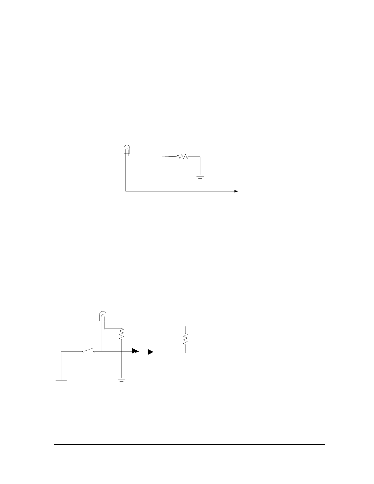
The MPCI specification states that the card will provide a 7mA source current for 3.3V LED
operation. Termination for the LED is as s umed to be on the O EM motherboard. Bel o w is a t ypica l
termination circuit for this LED:
470
Positive
terminal of LED
The operation of the LED is:
• Blinking regularly @ 3Sec intervals (3.3V) = Wireless client is not associated with the
network.
• Solid ON (3.3V) = Wireless client is associated with the network.
• OFF (low) = The WLAN card is does not have power or the wireless NIC is held in
RESET
Intel Confidential Page 7 of 13
Page 8
Intel Mini PCI Wireless Card Specification Revision 1.0c July 2, 2002
7.2 WLAN Activity Indicator
The LED_WLAN_ACT output signal fr om Pin12 of the M PCI system connector indicates wireless
LAN data activity. W hen the wireless client is as sociated, data traff ic will commence. The rate of
blink is determined b y the am ount of data activit y between th e access point and the wireless clie nt,
but will be fast enough at all times as to be clearly distinguishable between beacon activit y (re:
LINK) versus data traffic.
If the WLAN client is not associated with an access point, the LED will be solid OFF (Low).
The MPCI specification states that the card will provide a 7mA source current for 3.3V LED
operation. Termination for the LE D is as s umed to be on the O EM motherboard. Bel o w is a typical
termination circuit for this LED:
470
Positive
terminal of LED
The operation of the LED is:
• Rapidly blinking (3.3V) = Wireless client is passing data traffic to the access point.
• OFF (low) = The WLAN card is does not have power or the RF_Kill switch is active.
NOTE: The RF_Kill signal over rides Activity and drives this signal off (LOW)
7.3 Radio Transmitter Disable Switch
The HW_RadioXMIT_OFF# input sig na l o n Pi n13 of the Mini PCI system connector pro vi des t o the
OEM the opportunity to use a har dware implem entation to disable the RF portions of the Calexico
Mini PCI card. The OEM recommended circuit for implementation is shown in the diagram below.
3.3V
RF_Kill#
Mini PCI Card
The Mini PCI card will provide support circuitry necessary to clean up the drive signal (i.e.: debounce circuits and pull-up resistor) from the OEM platform.
Intel Confidential Page 8 of 13
Page 9
Intel Mini PCI Wireless Card Specification Revision 1.0c July 2, 2002
The Intel Mini PCI c ard will also “remember” the last switch position implemented. The las t user
setting (radio enable d or disabled, whether through software or har dware) should be “sticky” and
will be remembered by the Mini PCI card’s hardware/software across suspends, boots, power
cycles, etc. (driven via GPIO and firmware controlled). This will be accomplished with registry
entries for easy software tracking.
The operation of the Signal is:
• ON (3.3V) = The radio transmitter is ON (powered and enabled).
• OFF (low) = The radio transmitter is turned OFF, and made incapable of transmitting
unless the user performs some action to change the state of the radio (such as manually
changing the switch)
Note: The control of the radio tr ansmitter is an AND of the s oftware and hardware mec hanisms.
The radio transm itter must remain disable d unless BOTH the sof tware and hardware settin gs are
enabled for the radio transmitter.
SW Setting HW Switch Radio Transmitter Function
Enable Enable/High Enabled
Enable Disable/Low Disabled
Disable Enable/High Disabled
Disable Disable/Low Disabled
Note: The LINK and Activit y LE Ds (Pins 1 1 an d 12) s h oul d reflect normal operat io n of the Mi ni PCI
card unless the RF_Kill s witch and/or sof tware control pins are enab led. If either
the software control or RF_Kill hardware switches are enabled, both LINK and
Activity signals will be OFF (low).
7.4 Spectrum Indication Control Signal
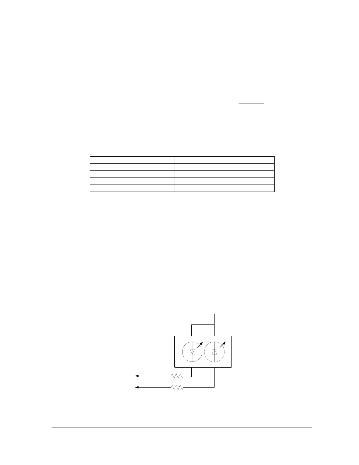
This CMOS driver is int ended to provide a control signal to a dual c olor LED. Depending on the
spectrum of radio op eration, this control signal will direct current flow through t he dual color LED
providing visual indication of which spectrum the wireless client is currently transmitting in. The
recommended OEM dual color LED implementation is shown below (note: an additional dualcolored LED circuit will be required for LINK/Association):
+3.3V
ACTIVITY
470
Spectrum Cntrl
The operation of the Spectrum Control signal is:
• ON (3.3V) = The radio 5.2GHz transmitter is ON and transmitting.
470
Intel Confidential Page 9 of 13
Page 10

Intel Mini PCI Wireless Card Specification Revision 1.0c July 2, 2002
• OFF (low) = The radio 2.4GHz transmitter is ON and transmitting.
7.5 Bluetooth Coexistence
Bluetooth priority information and 802.11b channel information are exchanged over a 2-wire
interface. The BT_Pr iority Signal and the Channe l_Clk Signal are multiplex on the same physical
interface with each signal transmitted in real-time and a coordinated manor. The Channel_Data
Signal transfers the cur r ent 802.1 1b c han ne l in us e , and indicates long- ter m channel inactivity, e.g.,
sleep modes to the Bluetooth module.
8. Mechanical
Intel’s Mini PCI cards s hould be design ed for the sm allest f orm-f actor pos sible to ensure m axim um
OEM platform c ompatibilit y. The target f orm-f actor is the Min i PCI type 3 B form -factor. If the car d
grows for additiona l capabil ity, max imum allowable c ard size if the Mini PCI type 3A f orm-f actor as
defined in the Mini PCI rev. 1.0 specification.
Due to OEM demand, the Hir ose U.FL-R-SMT (or equivalent) connector will be used on all Intel
Mini PCI cards to mate with cable connector U.FL- LP-066. The U.FL-R- SMT connector, thou gh it
meets the RF requirements for operation, vi ol ates the Mini PCI Z-dim ens ion by 0.1mm. Notificatio n
of this spec violation will be worked via the OEM channel using product mechanical specifications.
Mini PCI card shie lding re quir em ents wil l be rev iewed on a pr oject- by-proj ect b asis . No res tricti ons
will be placed upon the design team for RF shielding outside of Z-height restrictions.
8.1 PCB Card Design
The purpose of this Guide line is to insure the card properl y seats into a Mini-PCI Type III system
connector.
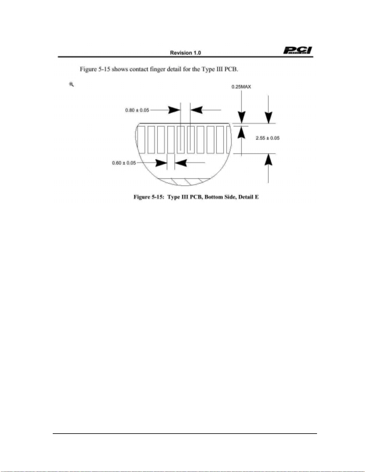
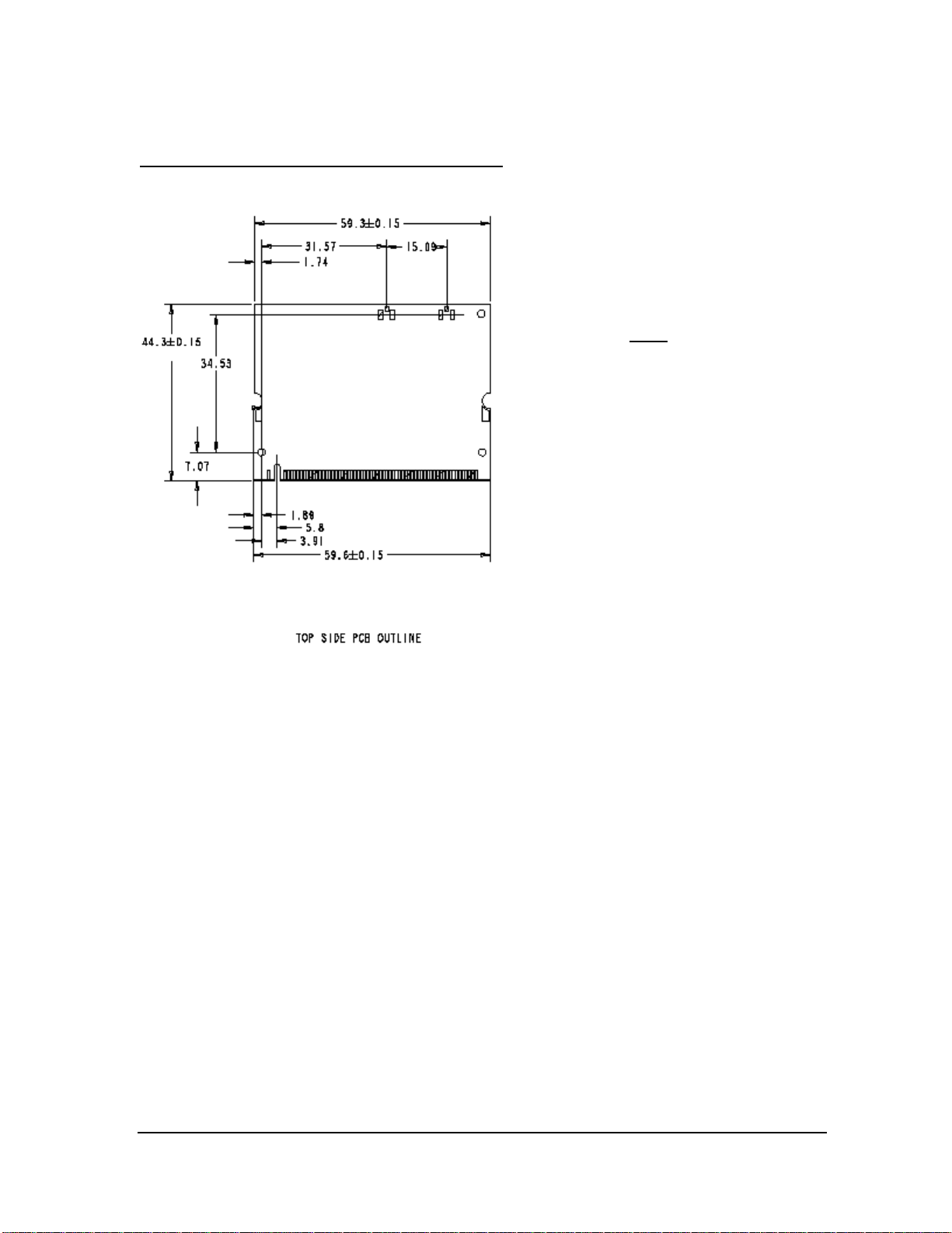
Connector Interface
Below is the m echanical information for the Min i PCI edge connector as it is s pecified within the
Mini PCI rev. 1.0 specification. The following sections detail Intel’s modifications from this
specification to improve the contact reliability for our customers.
Intel Confidential Page 10 of 13
Page 11
Intel Mini PCI Wireless Card Specification Revision 1.0c July 2, 2002
8.2 Antenna Connection
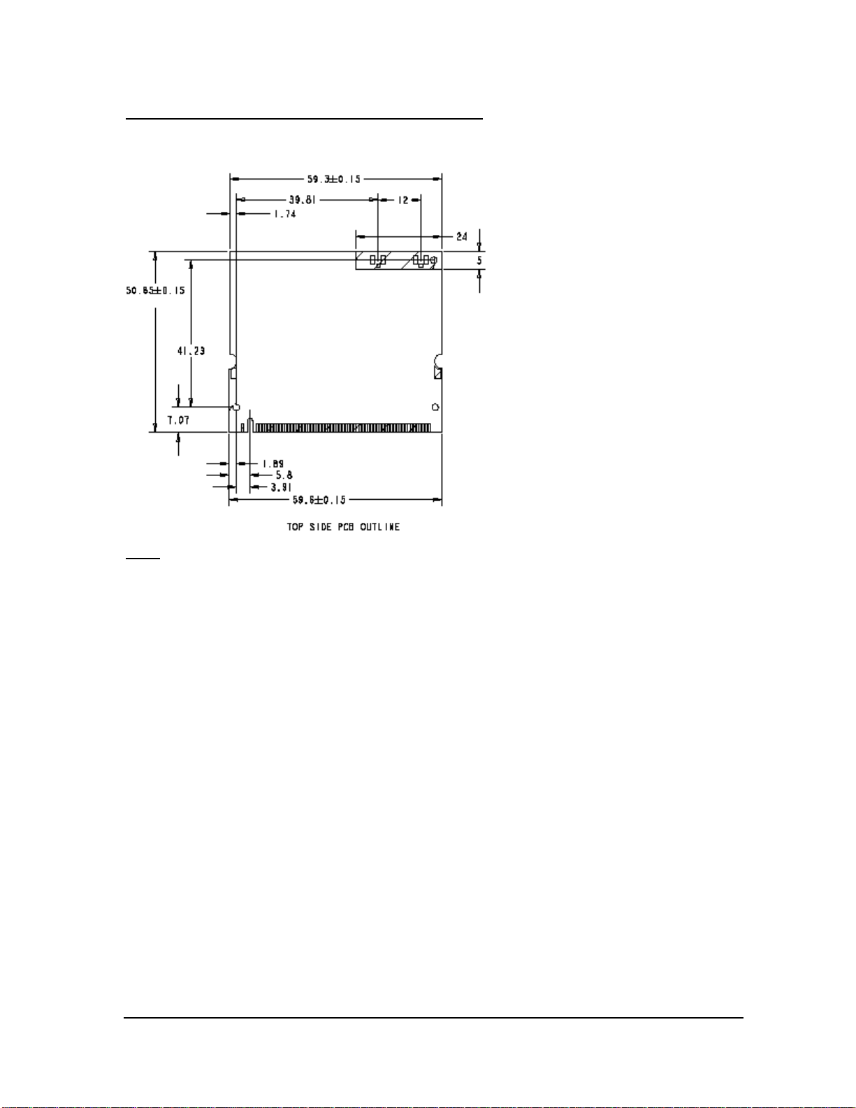
Antenna connector location s for both th e type 3 A and type 3B Mini P CI cards ar e illus trated b elow.
Intel’s 802.11 cards offer a diver sity antenna sc heme which allo ws for receivin g or transmitting on
either antenna. T he diagram shows a primary and s econdary antenna con nection which ref ers to
the default transmit antenna established by firmware.
Hirose style UL-F connec tor for attachment bet ween the Mini PCI card to the c o-ax c able attach ing
the antenna elements. The mechanical information is shown in figure X. Please note the
mechanical Z-dimension exceeds the current Mini PCI specification by 0.1mm. The OEM must
make allowances for this in their chassis design.
The figures belo w specify the Pr imary and Sec ondary antenn a connector loc ations on the type 3A
and type 3B Mini PCI car ds. Note tolerances f or anten na c on nec tor p lac ement for the type 3A c ard
will be +/- 1.0mm in the Y-dim ension only. X-dim ension tolerance is +/- 1.0mm. For the type 3B
card the tolerance will b e in creas ed for addition al des ign f lexib ilit y. Tolera nces for the type 3 B card
will be +/- 2.0mm in the Y-dim ension and in t he X-dimens ion tolerance is +/- 1.0mm. Com ponent
keep-out zone around the connectors for both form-factors will be a 5.0mm radius.
Intel Confidential Page 11 of 13
Page 12
Intel Mini PCI Wireless Card Specification Revision 1.0c July 2, 2002
Type 3A Mini PCI Antenna Connector Placement
Notes:
Dimensions in mm.
M refers to the MAIN.
A refers to the Auxiliary.
Intel Confidential Page 12 of 13
Page 13
Intel Mini PCI Wireless Card Specification Revision 1.0c July 2, 2002
Type 3B Mini PCI Antenna Connector Placement
Notes:
Dimensions in mm.
M refers to the MAIN.
A refers to the Auxiliary.
The card’s Prim ary and Secondary connectors will be clearl y silk-screened on the PCB as noted
above.
Intel Confidential Page 13 of 13
 Loading...