

Sony NW-E002F,NW-E005F,NW-E003F Service Manual
SERVICE MANUAL
Sony Corporation
Connect Business Division
Published by Sony Techno Create Corporation
US Model
Canadian Model
NW-E002F/E003F/E005F
AEP Model
NW-E002F/E003F
E Model
Chinese Model
Tourist Model
NW-E002F/E003F/E005F
DIGITAL MUSIC PLAYER
9-887-213-06
2006K16-1
© 2006.11
Ver. 1.5 2006.11
SPECIFICATIONS
NW-E002F/E003F/E005F
US and foreign patents licensed from
Dolby Laboratories.
HOME
Supported bit rates
MP3: 32 to 320 kbps variable bit rate-compliant
WMA: 32 to 192 kbps variable bit rate-compliant
ATRAC: 48/64/66 (ATRAC3)*/96/105 (ATRAC3)*/
128/132 (ATRAC3)/160/192/256/320/352 kbps
* CD recording cannot be done using SonicStage software
in ATRAC3 at 66/105 kbps.
Sampling frequency*
MP3: 32, 44.1, 48 kHz
WMA: 44.1 kHz
ATRAC: 44.1 kHz
* Sampling frequency may not correspond to all encoders.
Frequency response
20 to 20,000 Hz (single signal measurement)
FM Frequency range
87.5 to 108.0 MHz
IF (FM)
375 kHz
Antenna
Headphone cord antenna
Interface
Headphone: Stereo mini
Hi-speed USB (USB 2.0 compliant)
Operating temperature
5°C to 35°C (67°F to 95°F)
Power source
• Built-in rechargeable lithium-ion battery
• USB power (from a computer through the USB
connector of the player)
Battery life (continuous playback)*
ATRAC format: Approximately 28 hours (Playback at 132 kbps)
ATRAC format: Approximately 25 hours (Playback at 128 kbps)
ATRAC format: Approximately 27 hours (Playback at 48 kbps)
MP3 format: Approximately 27 hours (Playback at 128 kbps)
WMA format: Approximately 19 hours (Playback at 128 kbps)
FM radio reception: Approximately 8 hours
Dimension (w/h/d)
24.8 × 79.0 × 13.6 mm (1 × 3 1/8 × 9/16 inches)
(w/h/d, projecting parts not included)
Mass
Approx. 25 g (0.9 oz)
Audio compression technology
– MPEG-1 Audio Layer-3 (MP3)
– Windows Media Audio (WMA)
– Adaptive Transform Acoustic Coding (ATRAC)
Maximum recordable number of songs and time (Approx.)*
* When transferring four-minute songs.
NW-E002F NW-E003F
Bit rate Songs Time Songs Time
48 kbps 340 22 hr. 40 min. 685 45 hr. 00 min.
64 kbps 255 17 hr. 00 min. 515 34 hr. 20 min.
96 kbps 170 11 hr. 20 min. 345 23 hr. 00 min.
128 kbps 125 8 hr. 20 min. 260 17 hr. 20 min.
132 kbps 120 8 hr. 00 min. 250 16 hr. 40 min.
160 kbps 100 6 hr. 40 min. 205 13 hr. 40 min.
192 kbps 85 5 hr. 40 min. 170 11 hr. 20 min.
256 kbps 64 4 hr. 10 min. 130 8 hr. 40 min.
320 kbps 51 3 hr. 20 min. 100 6 hr. 40 min.
352 kbps 46 3 hr. 00 min. 94 6 hr. 10 min.
NW-E005F
Bit rate Songs Time
48 kbps 1,350 90 hr. 00 min.
64 kbps 1,000 66 hr. 40 min.
96 kbps 690 46 hr. 00 min.
128 kbps 520 34 hr. 40 min.
132 kbps 500 33 hr. 20 min.
160 kbps 415 27 hr. 40 min.
192 kbps 345 23 hr. 00 min.
256 kbps 260 17 hr. 20 min.
320 kbps 205 13 hr. 40 min.
352 kbps 185 12 hr. 20 min.
Capacity
Supplied accessories
(User available capacity)*
512 MB (Approx. 482 MB = 505,724,928 bytes)
1 GB (Approx. 968 MB = 1,015,726,080 bytes)
2 GB (Approx. 1.89 GB = 2,035,974,144 bytes)
* Available storage capacity of the player may vary.
A portion of the memory is used for data management
functions.
Headphones (1)
CD-ROM* (1)
- SonicStage software
- Operation Guide (PDF file)
Quick Start Guide (1)
* Do not attempt to play this CD-ROM in an audio CD
player.
Design and specifications are subject to change without
notice.
2
NW-E002F/E003F/E005F
TABLE OF CONTENTS
1. GENERAL ................................................................... 5
2. DISASSEMBLY
2-1. Disassembly Flow ........................................................... 6
2-2. Cabinet (Top) ................................................................... 7
2-3. Cabinet (Low) Assy ......................................................... 7
2-4. MAIN Board-1 ................................................................ 8
2-5. MAIN Board-2 ................................................................ 9
2-6. Battery (A) Assy.............................................................. 9
2-7. Organic EL Indicator Module ......................................... 10
3. TEST MODE ............................................................... 11
4. DIAGRAMS
4-1. Block Diagram ................................................................ 13
4-2. Printed Wiring Boards
– MAIN, SWITCH Board (Side A) –.............................. 14
4-3. Printed Wiring Boards
– MAIN, SWITCH Board (Side B) –.............................. 15
4-4. Schematic Diagram – MAIN Board (1/3) – ................... 16
4-5. Schematic Diagram – MAIN Board (2/3) – ................... 17
4-6. Schematic Diagram
– MAIN Board (3/3), SWITCH Board –......................... 18
5. EXPLODED VIEWS
5-1. Overall-1.......................................................................... 26
5-2. Overall-2.......................................................................... 27
5-3. Overall-3.......................................................................... 28
5-4. Overall-4.......................................................................... 29
6. ELECTRICAL PARTS LIST .................................. 30
UNLEADED SOLDER
Boards requiring use of unleaded solder are printed with the leadfree mark (LF) indicating the solder contains no lead.
(Caution: Some printed circuit boards may not come printed with
the lead free mark due to their particular size)
: LEAD FREE MARK
Unleaded solder has the following characteristics.
• Unleaded solder melts at a temperature about 40 °C higher
than ordinary solder.
Ordinary soldering irons can be used but the iron tip has to be
applied to the solder joint for a slightly longer time.
Soldering irons using a temperature regulator should be set to
about 350 °C.
Caution: The printed pattern (copper foil) may peel away if
the heated tip is applied for too long, so be careful!
• Strong viscosity
Unleaded solder is more viscou-s (sticky, less prone to flow)
than ordinary solder so use caution not to let solder bridges
occur such as on IC pins, etc.
• Usable with ordinary solder
It is best to use only unleaded solder but unleaded solder may
also be added to ordinary solder.
Flexible Circuit Board Repairing
• Keep the temperature of the soldering iron around 270 °C
during repairing.
• Do not touch the soldering iron on the same conductor of the
circuit board (within 3 times).
• Be careful not to apply force on the conductor when soldering
or unsoldering.
• Microsoft, Windows, Windows NT and Windows Media are trademarks or
registered trademarks of Microsoft Corporation in the United States and/or
other countries.
• Adobe and Adobe Reader are trademarks or registered trademarks of Adobe
Systems Incorporated in the United States and/or other countries.
• MPEG Layer-3 audio coding technology and patents licensed from
Fraunhofer IIS and Thomson.
• IBM and PC/AT are registered trademarks of International Business
Machines Corporation.
• Macintosh is a trademark of Apple Computer, Inc..
• Pentium is a trademark or a registered trademark of Intel Corporation.
• CD and music-related data from Gracenote, Inc., copyright © 2000-2004
Gracenote.
Gracenote CDDB
®
Client Software, copyright 2000-2004 Gracenote. This
product and service may practice one or more of the following U.S. Patents:
#5,987,525; #6,061,680; #6,154,773, #6,161,132, #6,230,192, #6,230,207,
#6,240,459, #6,330,593, and other patents issued or pending. Services
supplied and/or device manufactured under license for following Open
Globe,Inc. United States Patent 6,304,523. Gracenote and CDDB are
registered trademarks of Gracenote.
The Gracenote logo and logotype, and the “Powered by Gracenote” logo are
trademarks of Gracenote.
Notes on chip component replacement
• Never reuse a disconnected chip component.
• Notice that the minus side of a tantalum capacitor may be
damaged by heat.
Ver. 1.1
3
NW-E002F/E003F/E005F
Fig-1
Fig-2
NOTES ON ARRANGE THE OEL MODULE FLEXIBLE CABLE
pre-fold
SHEET (OEL-FPC), ADHESIVE
Remove protection sheet.
folding line
segment portion
SPACER (OEL)
1. Pre-fold the flexible cable as in Fig-1.
3. Make sure it does not cover the segment portion as in Fig-2.
2. Affix at the center of folding line and remove release SHEET (OEL-FPC), ADHESIVE.
Fold and press fit at the area of SHEET (OEL-FPC), ADHESIVE.
Remove protection sheet from OLED.
3mm
4.5mm
TABLE OF DESTINATION AND COLOR VARIATION
USNW-E002F
NW-E003F
BLACK SILVER PINK VIOLET GREEN BLUE
CND
AEP
E
KR
MX
US
CND
AEP
CEV
E
KR
MX
CEV
CN
JE
JE
CN
NW-E005F US
CND
E
KR
MX
JE
CN
• Abbreviation
CEV : Poland, Czech, Greece and Turkey models
CN : Chinese model
CND : Canadian model
KR : Korean model
MX : Mexican model
JE : Tourist model
Ver. 1.4
4
NW-E002F/E003F/E005F
Fig-1
Fig-3
Fig-4
Fig-2
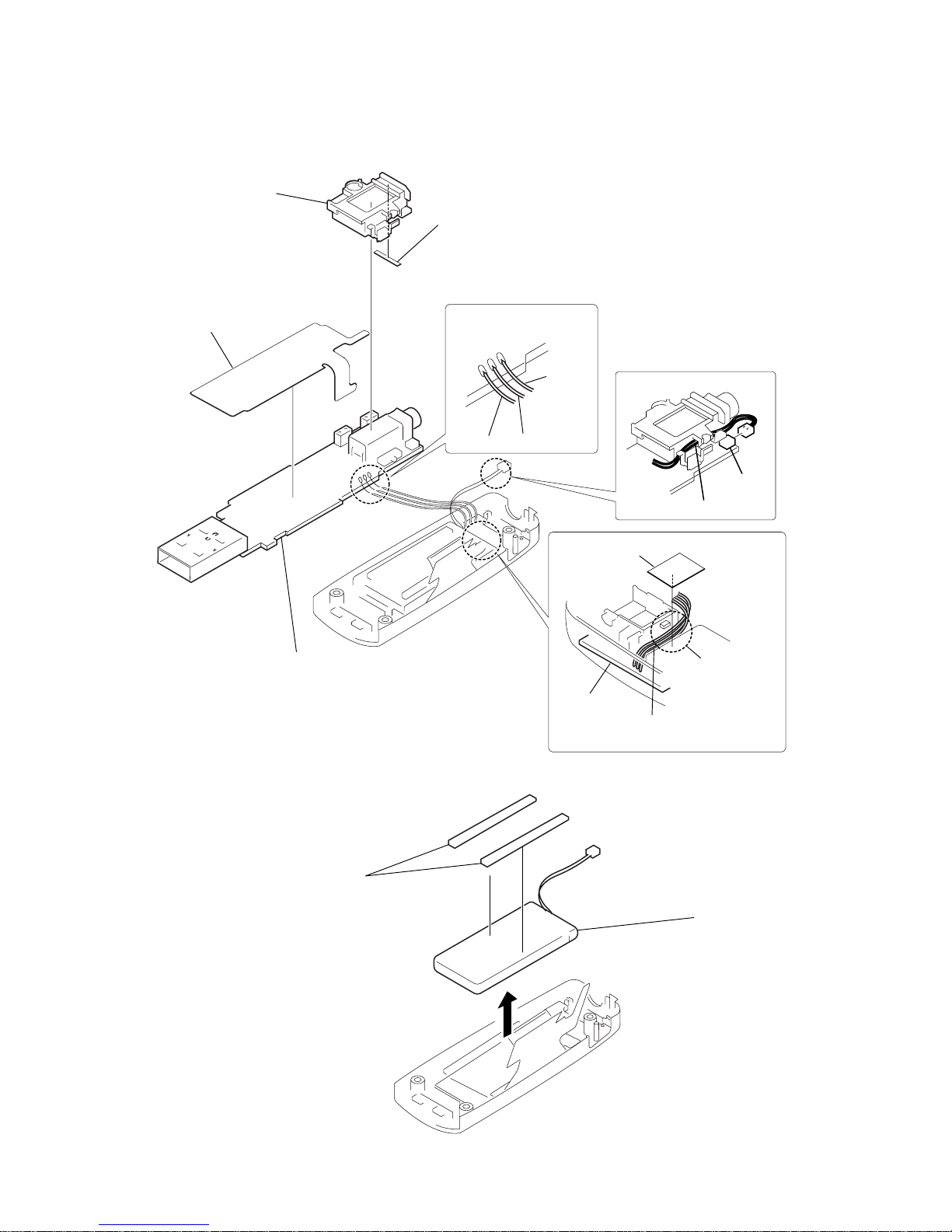
NOTES ON ARRANGE THE BATTERY WIRES AND SW PWB WIRES
HP GUIDE
HP GUIDE
BA TTERY WIRES
BA TTERY WIRES
BA TTERY WIRES
SW PWB WIRES
SW PWB WIRES
RIB
BA TTERY WIRES
1. Arrange BATTERY WIRES as in Fig-1 and Fig-2.
2. Arrange SW PWB WIRES to arrow direction (Fig-3) and attach the HP GUIDE.
3. Arrange BATTERY WIRES and SW PWB WIRES under the RIB as Fig-4 then attach the battery.
NOTES ON REPLACEMENT OF Ref. No. 15 (CABINET (MID) ASSY)
Ref. No. 15 has both the suffix-1 and the suffix-2 on part number.
Please confirm by the following two methods at replacement.
1. Whether it has Ref. No. 30 (HP GUIDE SHEET) or not.
• The one with Ref. No. 30 t Using the suffix-2 of Ref. No. 15.
• The one not with Ref. No. 30 t Using the suffix-1 of Ref. No.15.
2. Distinguish by the following serial number.
Suffix-2 is adopted since the following serial number.
NW-E002F : from 5076285
NW-E003F : from 5070762 t Using the suffix-2 of Ref. No. 15.
NW-E005F : from 5022246
Ver. 1.3
CAUTION
Danger of explosion if battery is incorrectly replaced.
Replace only with the same or equivalent type.
5
NW-E002F/E003F/E005F
SECTION 1
GENERAL
This section is extracted
from instruction manual.
6
NW-E002F/E003F/E005F
SECTION 2
DISASSEMBLY
Note: This set can be disassembled in the order shown below.
2-1. DISASSEMBLY FLOW
2-3. CABINET (LOW) ASSY
(Page 7)
2-4. MAIN BOARD-1
(Page 8)
2-5. MAIN BOARD-2
(Page 9)
2-6. BATTERY (A) ASSY
(Page 9)
2-7. ORGANIC EL INDICATOR
MODULE (Page 10)
2-2. CABINET (TOP)
(Page 7)
SET
Ver. 1.1
7
NW-E002F/E003F/E005F
Note: Follow the disassembly procedure in the numerical order given.
2-2. CABINET (TOP)
2-3. CABINET (LOW) ASSY
3
screw
2
sheet (VOL)
1
USB cover assy
5
cabinet (top)
4
eight claws
1
two screw
s
(M1.4)
4
four claws
2
rib
3
USB holder
9
cabinet (low) assy
5
sheet (HP)
6
button (VOL)
When installing knob (hold)
insert it in the groove.
knob (hold)
8
three adhesive sheets (cabinet)
7
spacer (lower)
8
NW-E002F/E003F/E005F
2-4. MAIN BOARD-1
3
two screws (B1.4)
1
two sheets immunity
2
sheet immunity
7
sheet (conductive)
4
two claws
6
sheet (static-C)
5
USB stay
9
connector (2P) (CN401)
8
Peel off the sheet (static-B).
0
button (F/R) ass
y
MAIN board
flat side
qa
organic EL indicator module
(39core) (CN601)
qs
Remove the MAIN board section
in the direction of the arrow.
9
NW-E002F/E003F/E005F
2-5. MAIN BOARD-2
2-6. BA TTERY (A) ASSY
6
Remove soldering from
the three points.
7
MAIN board
2
sheet (static)
3
HP guide
4
adhesive sheet (H.P)
5
cushion (wire)
red
white
blue
Note: Be careful not to damage
the harnesses.
Attach the cushon
(wire) after folding
back the harness.
SWITCH board
CN401
1
Remove the harness.
1
tow sheets
(BATT)
2
battery (A) assy
10
NW-E002F/E003F/E005F
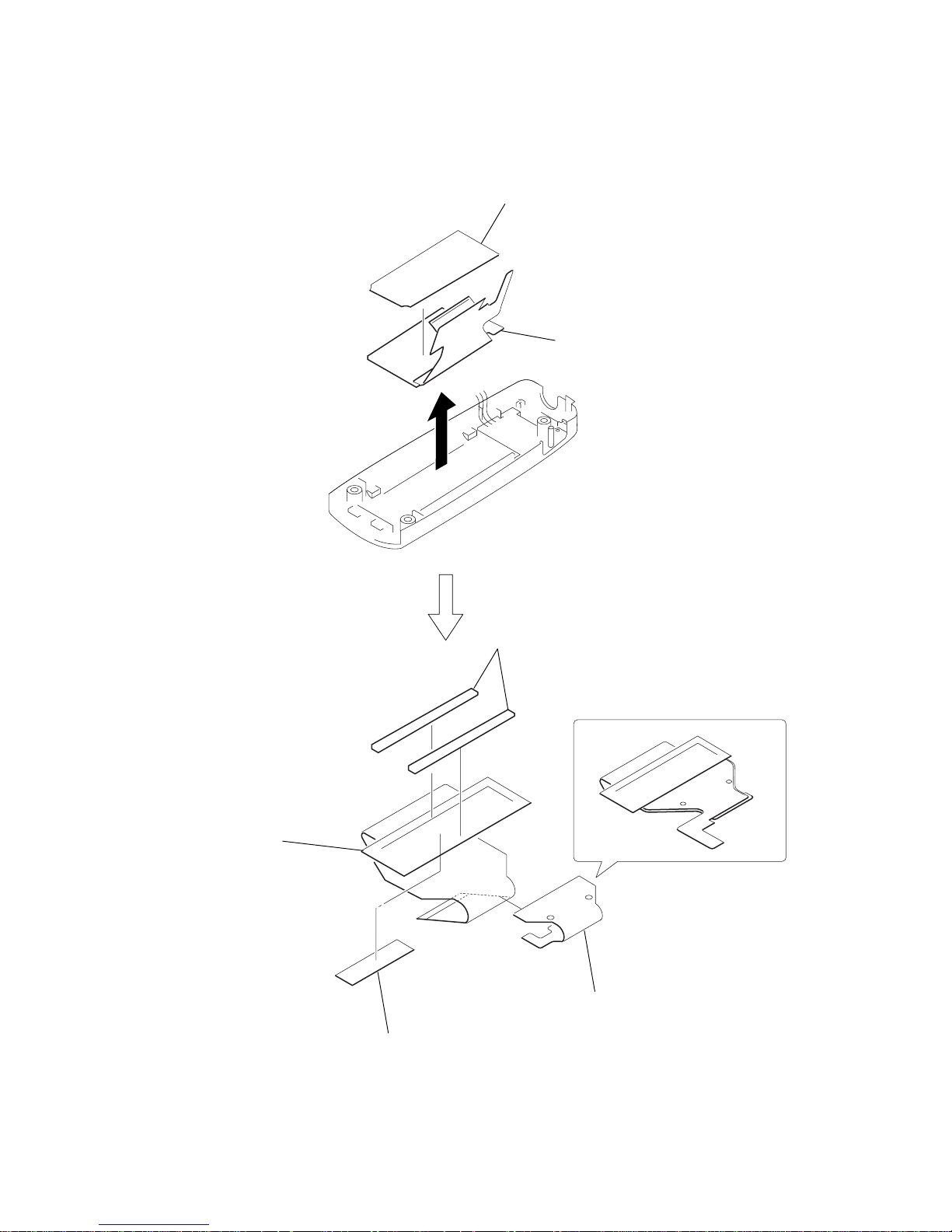
2-7. ORGANIC EL INDICATOR MODULE
1
sheet (OEL)
3
two spacers
2
OEL module sub assy
6
organic EL indicator module
5
adhesive sheet (OEL-FPC)
4
sheet (static-B)
Ver. 1.2
11
NW-E002F/E003F/E005F
SECTION 3
TEST MODE
1. HOW TO ENTER THE TEST MODE
1. Set the HOLD . switch in the HOLD ON position.
2. While keeping pressing the Nx and
HOME
buttons
in the HOLD ON position, press the RESET switch.
3. Then the characters “TEST MODE INITIALIZE..” is
displayed momentarily, and then the following indication is
displayed on screen.
“TEST MODE”
“0.8.04.00 [JP]”
2. HOW TO CHANGE THE TEST MODE
1. While the machine is in the TEST mode, set the HOLD .
switch from the ON to OFF position, or OFF to ON position.
2. Then test mode toggles and the following indication toggles
as shown below.
“TEST MODE (HOLD:OFF)” and
“TEST MODE (HOLD:ON)”
3. SYSTEM PARAMETER INITIALIZE
1. While the machine is in the TEST mode, press the
HOME
button.
2. Then the system parameter is initialized and the following
indication is displayed on screen.
“System Parameter Initialized.”
4. ALL KEY CHECK MODE
1. While the machine is in the TEST mode, press the Nx
button, and then the following indication is displayed on screen.
“ALL KEY CHECK”
“0x0001(ALL=0x00f3)”
2. Press the
HOME
button, then the hexadecimal number
2h is added and the following indication is displayed.
“0x0003(ALL=0x00f3)”
3. Press the – button, then the hexadecimal number 10h is added
and the following indication is displayed.
“0x0013(ALL=0x00f3)”
4. Press the + button, then the hexadecimal number 20h is added
and the following indication is displayed.
“0x0033(ALL=0x00f3)”
5. Press the > button, then the hexadecimal number 40h is
added and the following indication is displayed.
“0x0073(ALL=0x00f3)”
6. Press the . button, then the hexadecimal number 80h is
added then “0x00f3(ALL=0x00f3)” “KEYCHECK OK!”
displayed momentarily, and the machine exits the All Key
Check Mode and the Test Mode.
7. While the machine is in any step of step 2 to step 5 of the All
Key Check mode, press the Nx button.
8. Then “key check Canceled..” displayed momentarily, and the
All Key Check mode is stopped.
9. Re-press the Nx button, back to the original step the All
Key Check mode.
5. CHARGE CURRENT SELECT
1. While the machine is in the TEST MODE (HOLD:ON), press
the > button, the charge current and the indication toggles
as shown below.
“CHG: 100mA” and “CHG: 500mA”
6. CHARGE ON/OFF SELECT
1. While the machine is in the TEST MODE (HOLD:ON), insert
to the USB port on PC.
2. Press the . button, then the charge ON/OFF and the
indication toggles as shown below.
“CHG: start..” and “CHG: stop..”
7. BEEP ON/OFF CHECK
1. While the machine is in the TEST MODE (HOLD:ON), press
the + button.
2. Then the beep ON/OFF and the indication toggles as shown
below.
“BEEP: OFF” and “BEEP: ON”
3. When switch is set to “BEEP: OFF” from “BEEP: ON”, check
that the beep sound comes from headphone jack.
8. DISPLAY CHECK
1. While the machine is in the TEST MODE (HOLD:ON), press
the – button.
2. Then brightness of entire screen changes in the following order,
each time the – button is pressed.
Entire screen shows full brightness. (ALL ON)
Entire screen shows black screen. (ALL OFF)
Entire screen shows half brightness. (HALF ON)
9. TUNER ON/OFF CHECK
1. While the machine is in the TEST MODE (HOLD:OFF), press
the > button.
2. Then tuner ON/OFF and the indication toggles as shown below .
“Tuner: ON” and “Tuner: OFF”
3. When “Tuner: ON” mode, check that the FM broadcast is
output from headphone jack.
10. FM RECEPTION FREQUENCY CHECK
1. While the machine is in the TEST MODE (HOLD:OFF), press
the . button.
2. Press the . button. Each time the . button is pressed,
the frequencies are checked and the following indication is
displayed as shown below.
“TUNER Freq. t CENTER (91.00MHz)”
“TUNER Freq. t MAX (107.75MHz)”
“TUNER Freq. t MIN (76.00MHz)”
11. SLEEP CHECK
1. While the machine is in the TEST MODE (HOLD:OFF), press
the + button.
2. Then “SLEEP IN” displayed momentarily, and the machine
enters the sleep mode.
3. While the machine is in the sleep mode, press any button.
4. Then “SLEEP OUT” displayed momentarily, the machine exits
the sleep mode and enters the test mode of the pressed key.
12. INFORMATION CHECK
1. While the machine is in the TEST MODE (HOLD:OFF), press
the – button to enter the information mode.
2. Each time the – button is pressed, various information are
checked in the following order.
“VERSION: 0.8.04.00”
“BOOTs VERSION: 0.4”
“SHIMUKE: JP”
“HWCONF: m:02h v:0h”
“Storage: 512MB”
“TUNER: YES”
“SVN VERSION: 1600:1601S”
13. HOW TO EXIT THE TEST MODE
Press the RESET switch in any state to exit the test mode.
12
NW-E002F/E003F/E005F
SECTION 4
DIAGRAMS
Note on Schematic Diagram:
• All capacitors are in µF unless otherwise noted. (p: pF) 50 WV
or less are not indicated except for electrolytics and tantalums.
• All resistors are in Ω and 1/
4
W or less unless otherwise speci-
fied.
•%: indicates tolerance.
• C : panel designation.
• : B+ Line.
•Voltages and waveforms are dc with respect to ground under
no-signal (detuned) conditions.
no mark : PLAY
•Voltages are taken with a VOM (Input impedance 10 MΩ).
Voltage v ariations may be noted due to normal production tolerances.
•Waveforms are taken with a oscilloscope.
Voltage v ariations may be noted due to normal production tolerances.
• Circled numbers refer to waveforms.
• Signal path.
J : PLAY BACK
F : FM
Note on Printed Wiring Board
• X : parts extracted from the component side.
• Y : parts extracted from the conductor side.
• : Pattern from the side which enables seeing.
Caution:
Parts face side: Parts on the parts face side seen from
(Side A) the parts face are indicated.
Pattern face side: P arts on the pattern face side seen from
(Side B) the pattern face are indicated.
• These boards are multi-layer printed board.
However, the patterns of intermediate-layer have not been included in the diagram.
*
Replacement of IC101, IC201 on MAIN board requires
a special tool.
• Lead Layouts
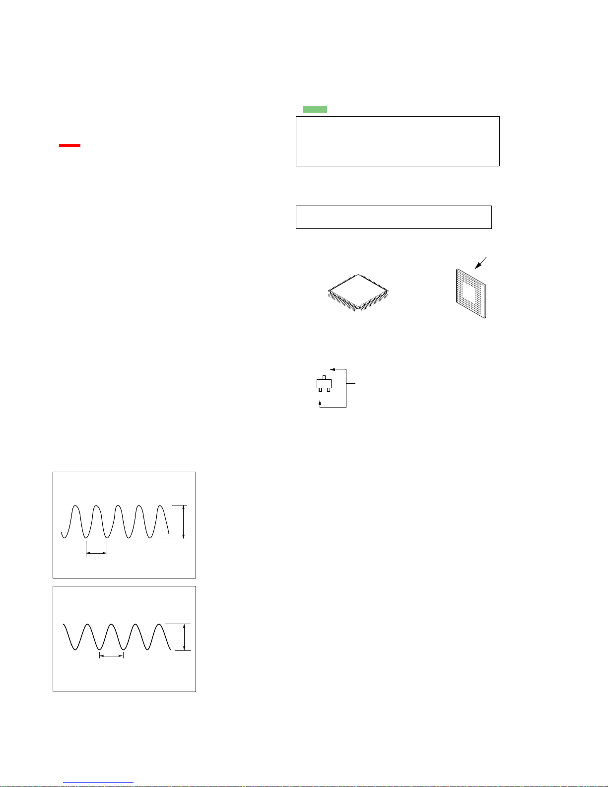
• Indication of transistor.
surface
CSP (Chip Size Package)Lead layout of conventional IC
C
B
These are omitted.
E
Q
• Waveforms
– MAIN Board –
1
IC101 <zz, (TEX)
200 mV/DIV, 40 ns/DIV
0.8 Vp-p
83.3 ns
2
IC101 <zzb (EXTAL)
22.2 ns
0.8 Vp-p
200 mV/DIV, 10 ns/DIV
1313
NW-E002F/E003F/E005F
NW-E002F/E003F/E005F
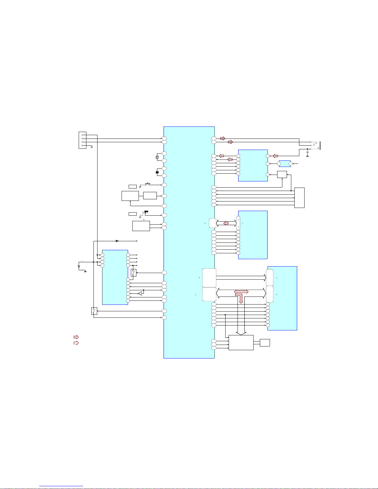
4-1. BLOCK DIAGRAM
• Signal Path
: PLAY BACK
: FM
CN101
USB
CONNECTOR
VBUS
DATA-
GND
DATA+
TUNER
IC2702
DM
126
125
118
119
DP
X101
12MHz
RESET
HOLD
ON OFF
TX
TEX
AOUT R
6
AOUT L
5
DA
7
LA
8
CL
9
STO
ANT
13
2
HPOUTL
HPOUTR
115
116
X102
45.1584MHz
XTAL
259
CRST1A
39
GPION1/INT9
EXTAL
1VCC
10X1
VDD IO2.8
J101
RECHARGEABLE
BATTERY
Li-ion
1PCS, 3.7V 700mA
IC601
POWER CONTROL
D601
IC2701
13
DRIVE
Q401
36
33
SIO/GPIOG1
SCKO
134
132
CS4/GPIOA25
235
SCS0/GPIOG2
SO0/GPIOG0
133
135
MICINL
MICINR
186
183
136
9
1 - 8
88
138
87
248
I/O1
I/O8
NAND FLASH ROM
IC1301
CLE
16
10
ALE
17
16
XWE
18
17
XWP
19
18
R/B1
7
15
XRE
8
11
XCE1
9
29
32
41
.
44
236
204 - 211,
222 - 229
31,32
37-41
44,45
48,49
51-53
55,56
DQ0
DQ15
32MB FLASH ROM & 4MB SRAM
IC201
161 - 176,
195 - 199
1
5-8
12-17
19-21
23-27
29,34
A0
A20
A1
A21
ORGANIC EL
INDICATOR
MODULE
XOE
36
231
XCE1F
35
265
XRSTF
10
237
XWE
4
232
XCE1S
43
239
XUB
9
238
XLB
2
233
91
90
GATE
Q2701
RTC
X801
38
GPION0/INT8
77
AN0
FUNCTION
KEY
S501 - 504
40
GPION2/INT10
FUNCTION
KEY
41
GPION3/INT11
89
GPIOF2
102
MSDIO2/GPIOE3
103
MSDIO3/GPIOE4
101
MSDIO1/GPIOE2
29
RST2OUT
127
VBUS/GPIOD0
230
WAIT/GPIOA20
84
AN7
USB IN2
4
USB IN1
VDD AD 2.0
VDD CORE 1.2
VDD IO 2.8
3
BAT1
7
BAT2
8
OUT AD 17
28LX CORE
VDD USB 3.3
OUT USB3.3
35
VDD UNREG
24LX IO
26OUT CORE
2USB H/L
9XCHG STAT
10XCHG EN
20IU3
30EN
40USB POK
Q601,602
Q604
Q605
IC101
SYSTEM CONTROLLER
NAND FLASH INTERFACE
USB INTERFACE
A/D, D/A CONVERTER
SERIAL INTERFACE
S101
S505
+2.7V
REG
(
(
HEADPHONES
JACK
(
(
Q501, 502
SWITCH
D0/GPIOA4
D15/GPIOA19
SDDAT3/INT5/GPIOF4
SDDAT2/INT4/GPIOF3
RE/GPIOA26
CS0/GPIOA21
RST
WE/GPIOA27
CS1/GPIOA22
UB/GPIOA29
LB/GPIOA28
CS2/GPIOA23
NCLE/GPIOC8
NALE/GPIOC9
NWE/GPIOC15
NWP/GPIOC16
NRB0/GPIOC17
NRE/GPIOC14
NCE0/GPIOC10
NAND0/GPIOC0
NAND7/GPIOC7
SI1/GPIOH1
SCK1
DREQ/INT2/GPIOF1
OSCIN
INT1/GPIOF0
1414
NW-E002F/E003F/E005F
NW-E002F/E003F/E005F
4-2. PRINTED WIRING BOARDS – MAIN, SWITCH BOARD (SIDE A) –
:Uses unleaded solder.
• Semiconductor
Location
Ref. No.
Location
D601 D-11
IC101 C-4
IC1301 C-8
IC2701 E-9
Q501 E-4
Q502 E-3
Q602 E-9
Q2701 E-8
*
IC101
IC1301
IC2701
*
CSP
(Chip Size Package)
MAIN BOARD
(SIDE A)
BLUE
WHITE
RED
4
USB
CONNECTOR
1
(
(
E
E
1
16
34
6
12 7
E
GS
D
G
2
1
S
D
SWITCH BOARD
(SIDE A)
HOLD
1-870-341-
(11)
RECHARGEABLE
BATTERY Li-ion
1PCS, 3.7V
700mA
OFF ON
.
>
11
1-870-355-
(11)
21
E005F
E003F/E005F
E005F
E003F/E005F
CN101
C115
C155
R126
C118
R111
R2115
C120
C119
R110
C162
LF101
C102
C104
JL102
R510
VDR106
JL103
Q502
Q501
C114
JL101
R514
R101
R515
C107
R102
C123
C110
R103
R114
R513
C124
VDR108
C620
R112
JL108
JL110
JL109
C619
R802
FB104
VDR105
VDR107
C159
C125
R113
C126
C136
C153
R1303
C801
JL801 JL802
X101
C156
R129
R1301
X102
R122
C154
R124
C111C134
R120
R1302
R1305
C152
C144
R1306
C150
C137
C1301 R1304
R803
C140
C139
R507
R511
R506
R504
R801
Q2701
X801
R2709
Q602
R2707
C2701
C2702
R602
R2704
JL504
JL503
JL505
D601
R501
C501
VDR501
R505
S505
R512
R503
R509
R502
R508
S504
S503
CN601
JL903
JL901
JL902
1
A
B
C
D
E
F
G
H
I
J
2 3 4 5 6 7 8 9 10 11 12 13 14 15
*
Replacement of IC101 on MAIN board requires a
special tool.
 Loading...