

Page 1
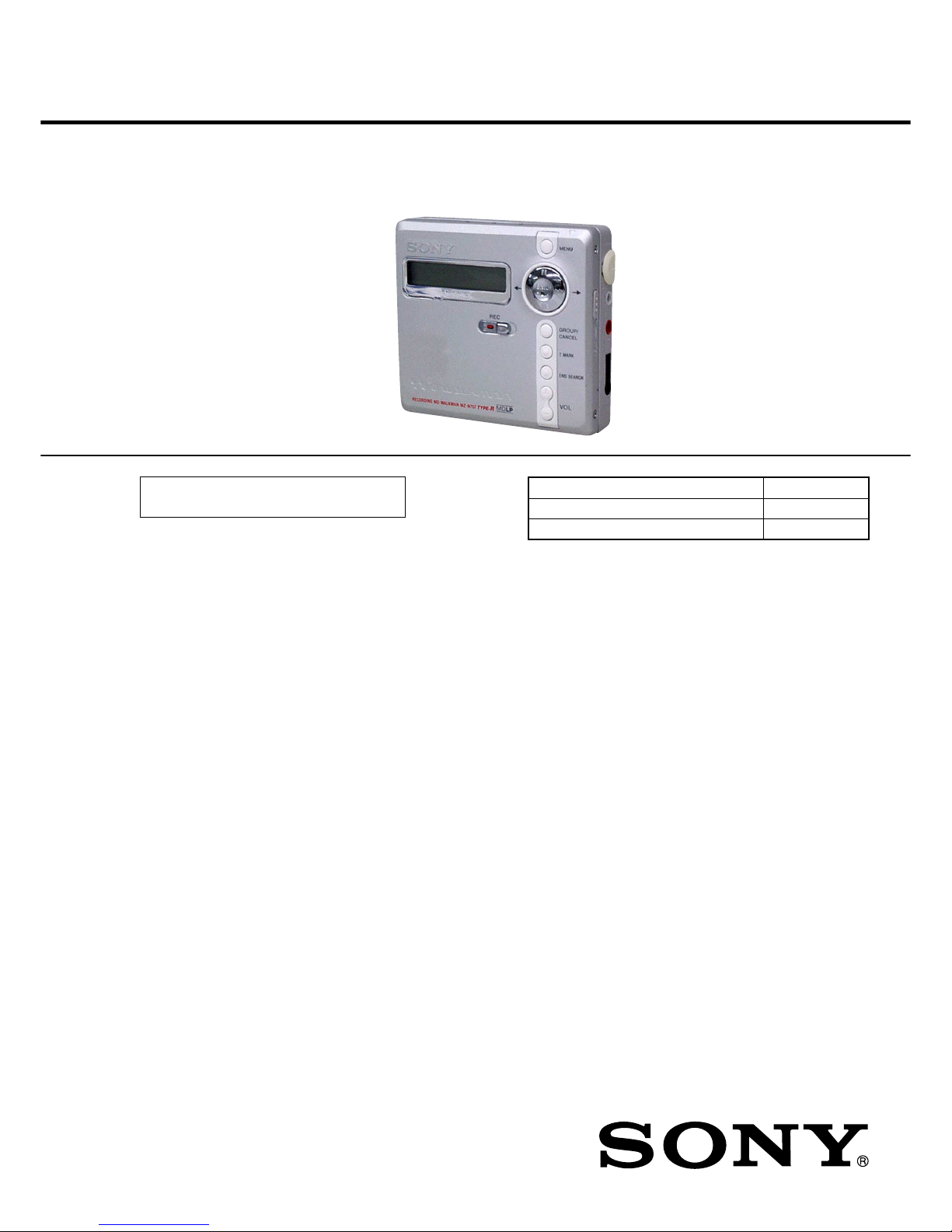
SERVICE MANUAL
PORTABLE MINIDISC RECORDER
US Model
Canadian Model
AEP Model
UK Model
SPECIFICATIONS
MZ-N707
US and foreign patents licensed from Dolby
Laboratories.
– Continued on next page –
Model Name Using Similar Mechanism NEW
Mechanism Type MT-MZN707-177
Optical Pick-up Name LCX-5R
Ver 1.0 2002. 01
9-873-458-01 Sony Corporation
2002A0500-1 Personal Audio Company
C 2002.1 Published by Sony Engineering Corporation
• OpenMG, “MagicGate”, “MagicGate Memory Stick”, “Memory Stick”,
VAIO,MusicClip and their logos are trademarks of Sony Corporation.
• “WALKMAN” is a trademark of Sony Corporation.
• Microsoft,Windows,Windows NT and Windows Media are trademarks
or registered trademarks of Microsoft Corporation in the United States
and/or other countries.
• IBM and PC/AT are registered trademarks of International Business
Machines Corporation.
• Macintosh is a trademark of Apple Computer,Inc.in the United States
and/or other countries.
• All other trademarks are trademarks of their respective owners. ™ and
® marks are omitted in this manual.
MD Recorder
Audio playing system
MiniDisc digital audio system
Laser diode properties
Material: GaAlAs MQW
Wavelength:
λ = 790 nm
Emission duration: continuous
Laser output: less than 44.6 µW
(This output is the valu e measure d at a dist ance
of 200 mm from the lens surface o n the optic a l
pick-up block with 7 mm aperture.)
Recording and playback time
When using MDW-80
Maximum 160 min. in monaural
Maximum 320 min. in stere o
Revolutions
Approx. 380 rpm to 2,700 rpm (CLV)
Error correction
ACIRC (Advanced Cross Interleave Reed
Solomon Code)
Sampling frequency
44.1 kHz
Sampling rate converter
Input: 32 kHz/44.1 kHz/48 kHz
Coding
ATRAC (Adaptive TRansform Acoustic
Coding)
ATR AC3 — LP2
ATR AC3 — LP4
Page 2
2
MZ-N707
Modulation system
EFM (Eight to Fourteen Modulation)
Number of channels
2 stereo channels
1 monaural channel
Frequency response
20 to 20,000 Hz ± 3 dB
Wow and Flutter
Below measurable limit
Inputs
Microphone: stereo mini-ja ck , minimum input
level 0.35 mV
Line in: stereo mini- jack, minimum input level
49 mV
Optical (Digital) in: optical (digital) mini-jack
Output
i: stereo mini-jack, m aximum output level
5mW+5mW, load impedance 16 ohm (except US model)
5mW+5mW, load impedance 24 ohm (US model)
General
Power requirements
Sony AC Power Adaptor connected at the DC
IN 3 V jack (country model in parenthese s):
120 V AC, 60 Hz (USA, Canada)
230 V AC, 50/60 Hz (Continental Europe)
230 - 240 V AC, 50 Hz (U.K.)
Nickel Cadmium rechargeable battery NCWMAA (supplied)
LR6 (size AA) alkaline battery (not supplied)
Dimensions
Approx. 81 × 74.4 × 27.7 mm (w/h/d) (31/4 × 3
× 1
1
/8 in.) without projections.
Mass
Approx. 116 g (4.1 oz) the recorder only
Supplied accessories
NC-WMAA Nickel Cadmium rechargeable battery (1)
AC power adaptor (1)
Headphones/ear phones with a remote cont rol (1)
Battery charging stand (1)
Optical cable (1)
USB cable (1)
CD-ROM (1)*
Carrying case with a belt clip (1) (except US model)
Battery carrying case (1)
Carrying pouch (1) (US and Canadian models)
Car connecting pack (1) (US and Canadian models)
Blank Minidisc (1) (US and Canadian models)
Design and specifications are subject to change
without notice.
Car battery cord (1) (US and Canadian models)
∗ Do not play a CD-ROM on an audio CD player.
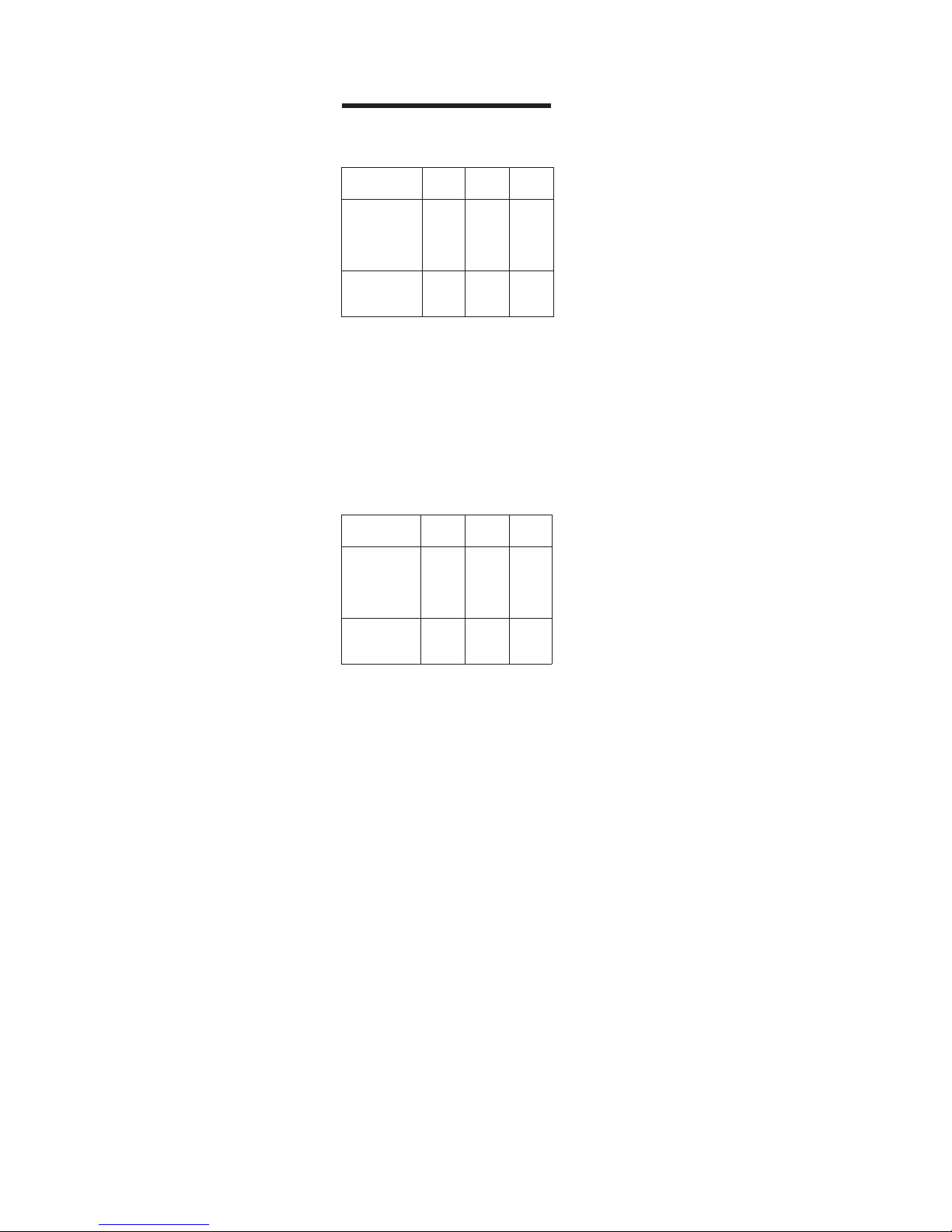
Battery life
1)
When recording
2)
(Unit: approx.hours)(JEITA3))
1)
The battery life may be shorter due to operating
conditions, the temperature of the location, and
varieties of batteries.
2)
When you record, use a fully charged
rechargeable batter y. Reco rd ing time may
differ according to the alkaline batteries.
3)
Measured in accordance wit h the JEITA (Japan
Electronics and Information Technolo gy
Industries Association) standard.
Batteries SP
Stereo
LP2
Stereo
LP4
Stereo
NC-WMAA
Nickel
Cadmium
rechargeable
battery
4)
4)
When using a 100% fully charged rechargeable
battery.
4 6 7.5
LR6 (SG)
Sony alkaline
dry battery
5)
5)
When using a Sony LR6 (SG) “STAMINA”
alkaline dry battery (produced in Japa n) .
91316
When playing
(Unit: approx.hours)(JEITA1))
Batteries SP
Stereo
LP2
Stereo
LP4
Stereo
NC-WMAA
Nickel
Cadmium
rechargeable
battery
2)
15 16 20
LR6 (SG)
Sony alkaline
dry battery
3)
42 48 56
1)
Measured in accordance with the JEITA
(Japan Electronics and Information
Technology Industries Associat io n ) stan d ard .
2)
When using a 100% fully charged
rechargeable battery.
3)
When using a Sony LR6 (SG) “STAMINA”
alkaline dry battery (produced in Japa n) .
ATTENTION AU COMPOSANT AYANT RAPPORT
À LA SÉCURITÉ!
LES COMPOSANTS IDENTIFIÉS PAR UNE MARQ UE 0
SUR LES DIAGRAMMES SCHÉMA TIQUES ET LA LISTE
DES PIÈCES SONT CRITIQUES POUR LA SÉCURITÉ
DE FONCTIONNEMENT. NE REMPLACER CES COMPOSANTS QUE PAR DES PIÈCES SONY DONT LES
NUMÉROS SONT DONNÉS DANS CE MANUEL OU
DANS LES SUPPLÉMENTS PUBLIÉS PAR SONY.
SAFETY-RELATED COMPONENT WARNING!!
COMPONENTS IDENTIFIED BY MARK 0 OR DOTTED
LINE WITH MARK 0 ON THE SCHEMATIC DIAGRAMS
AND IN THE PARTS LIST ARE CRITICAL TO SAFE
OPERATION. REPLACE THESE COMPONENTS WITH
SONY PARTS WHOSE PART NUMBERS APPEAR AS
SHOWN IN THIS MANU AL OR IN SUPPLEMENTS PUBLISHED BY SONY.
Page 3

3
MZ-N707
On power sources
• Use house current, Nickel Cadmium
rechargeable battery, LR6 (SG) battery, or car
battery.
• For use in your house: Use the AC power
adaptor supplied with this r ecor de r. Do not
use any other AC power adaptor since it may
cause the recorder to malfunction.
Polarity of the
plug
TABLE OF CONTENTS
1. SERVICING NOTES............................................... 4
2. GENERAL ................................................................... 5
3. DISASSEMBLY
3-1. Disassembly Flow ........................................................... 6
3-2. Case (Lower) ................................................................... 7
3-3. Upper Panel Section........................................................ 7
3-4. LCD Module, Upper Panel Sub Assy............................. 8
3-5. Mechanism Deck (MT-MZN707-177) ........................... 8
3-6. Set Chassis (5192) Assy.................................................. 9
3-7. MAIN Board ................................................................... 9
3-8. OP Service Assy (LCX-5R)............................................ 10
3-9. Holder Assy ..................................................................... 11
3-10. DC Motor (Sled) (M602) ................................................ 11
3-11. DC SSM18B Motor (Spindle) (M601),
DC Motor (Over Write Head Up/Down) (M603) .......... 12
4. TEST MODE.............................................................. 13
5. ELECTRICAL ADJUSTMENTS......................... 19
6. DIAGRAMS
6-1. Block Diagram – SERVO/USB Section – ...................... 32
6-2. Block Diagram – AUDIO Section – ............................... 33
6-3. Block Diagram – DISPLAY/KEY CONTROL/
POWER SUPPLY Section – ........................................... 34
6-4. Note for Printed Wiring Board and
Schematic Diagrams ....................................................... 35
6-5. Printed Wiring Board
– MAIN Board (Component Side) – ............................. 36
6-6. Printed Wiring Board
– MAIN Board (Conductor Side) – ............................... 37
6-7. Schematic Diagram – MAIN Board (1/4) – .................. 38
6-8. Schematic Diagram – MAIN Board (2/4) – .................. 39
6-9. Schematic Diagram – MAIN Board (3/4) – .................. 40
6-10. Schematic Diagram – MAIN Board (4/4) – .................. 41
6-11. IC Pin Function Description ........................................... 48
7. EXPLODED VIEWS
7-1. Upper Panel, Case (Lower) Section ............................... 55
7-2. Chassis Section ............................................................... 56
7-3. MAIN Board Section ...................................................... 57
7-4. Mechanism Deck Section-1 (MT-MZN707-177)........... 58
7-5. Mechanism Deck Section-2 (MT-MZN707-177)........... 59
8. ELECTRICAL PARTS LIST ............................... 60
CAUTION
Use of controls or adjustments or performance of procedures
other than those specified herein may result in hazardous radiation exposure.
Notes on chip component replacement
• Never reuse a disconnected chip component.
• Notice that the minus side of a tantalum capacitor may be dam-
aged by heat.
Flexible Circuit Board Repairing
• Keep the temperature of the soldering iron around 270 ˚C during repairing.
• Do not touch the soldering iron on the same conductor of the
circuit board (within 3 times).
• Be careful not to apply force on the conductor when soldering
or unsoldering.
UNLEADED SOLDER
Boards requiring use of unleaded solder are printed with the leadfree mark (LF) indicating the solder contains no lead.
(Caution: Some printed circuit boards may not come printed with
the lead free mark due to their particular size)
: LEAD FREE MARK
Unleaded solder has the following characteristics.
• Unleaded solder melts at a temperature about 40 ˚C higher than
ordinary solder.
Ordinary soldering irons can be used but the iron tip has to be
applied to the solder joint for a slightly longer time.
Soldering irons using a temperature regulator should be set to
about 350 ˚C .
Caution: The printed pattern (copper foil) may peel away if the
heated tip is applied for too long, so be careful!
• Strong viscosity
Unleaded solder is more viscous (sticky , less prone to flow) than
ordinary solder so use caution not to let solder bridges occur
such as on IC pins, etc.
• Usable with ordinary solder
It is best to use only unleaded solder but unleaded solder may
also be added to ordinary solder.
Page 4
4
MZ-N707
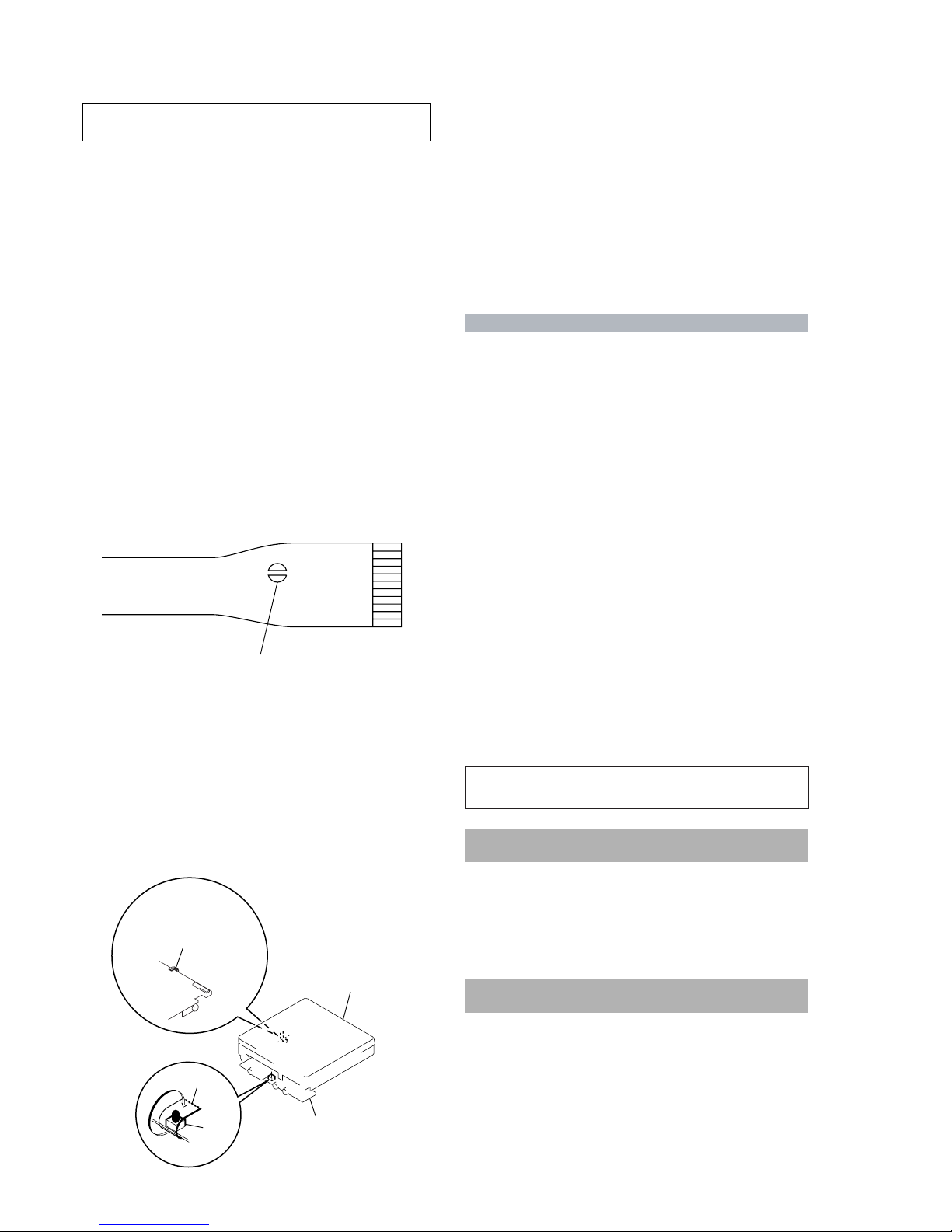
NOTES ON HANDLING THE OPTICAL PICK-UP
BLOCK OR BASE UNIT
The laser diode in the optical pick-up block may suffer electrostatic break-down because of the potential difference generated
by the charged electrostatic load, etc. on clothing and the human
body.
During repair, pay attention to electrostatic break-down and also
use the procedure in the printed matter which is included in the
repair parts.
The flexible board is easily damaged and should be handled with
care.
NOTES ON LASER DIODE EMISSION CHECK
Never look into the laser diode emission from right above when
checking it for adjustment. It is feared that you will lose your sight.
NOTES ON HANDLING THE OPTICAL PICK-UP BLOCK
(LCX-5R)
The laser diode in the optical pick-up block may suffer electrostatic break-down easily. When handling it, perform soldering
bridge to the laser-tap on the flexible board. Also perform measures against electrostatic break-down sufficiently before the operation. The flexible board is easily damaged and should be handled
with care.
OPTICAL PICK-UP FLEXIBLE BOARD
SECTION 1
SERVICING NOTES
• In performing the repair with the power supplied to the set, removing the MAIN board causes the set to be disabled.
In such a case, fix a conve x part of the open/close detect switch
(S806 on MAIN board) with a tape in advance.
Handle the FLEXIBLE board (over write head) with care, as it
has been soldered directly to the MAIN board.
In repairing the component side of MAIN board, connect the
FLEXIBLE board (over write head) and the MAIN board with
the lead wires in advance.
laser-tap
• Replacement of CXD2677-202GA (IC801) used in this set requires a special tool.
• The shipment data will be cleared when the NV is reset. Therefore, change the NV adjusted values following the Change of
NV Adjusted Values immediately after the NV was reset. (See
page 19)
• This set requires the patch data in the nonvolatile memory
(IC804) to be rewritten using the application, when the MAIN
board or nonvolatile memory (IC804) was replaced. (See page
29)
System requirements
• IBM PC/AT or Compatible (The software does not run on Macintosh.)
CPU: MMX™ Pentium
®
233 MHz or higher (Pentium® II 400 MHz or higher is
recommended.)
Hard disk drive space: 60 MB or more (The amount of necessary space depends on
the version of the Windows OS or the size of your audio files.)
RAM: 64 MB or higher (128 MB or higher is recommended for Windows
®
XP Home
Edition/Windows
®
XP Professional.)
CD-ROM drive (capable of digital playback by WDM)
Sound Board
USB port (supports USB 2.0 Full Speed (previously USB 1.1))
• Operating System: Windows
®
98/Windows® 98 Second Edition/Windows® 2000
Professional/Windows
®
Me/Windows® XP Home Edition/Windows® XP
Professional (manufacturer installed)
The NTFS format of Windows
®
2000 Professional, Windows® XP Home Edition, or
Windows
®
XP Professional (manufacturer-installed) is supported only when used
with the standard (factory) settings.
This software is not supported by the following environments.
– Windows
®
95, Windows® NT, or other versions of Windows® NT (such as Server)
– An environment that is an upgrade of the original manufacturer-installed
operating system, as in the following examples:
Windows
®
3.1/Windows® 95 t Windows® 98 (or Windows® 98 Second Edition/
Windows
®
Me)
Windows
®
Me/Windows® 2000 Professional t Windows® XP
– Multi-boot environment with Windows
®
2000 (or Windows® XP) and Windows
®
98 (or Windows® 98 Second Edition/Windows®Me)
• Display: High (16bit) Color or more (800 × 480 dot or more)
• Internet access: for Web registration and EMD services
• Internet access: for software upgrades and CDDB2 use. (US and Canadian models)
• Windows Media Player (version 7.0 or higher) installed for playing WMA files.
Notes
• Trouble-free operation is not assured within a multiple-monitor environment.
• We do not assure trouble-free operation for all computers satisfying the system requirements.
• Trouble-free operation is not guaranteed following the self-conducted upgrade of home-built
PCs or operating systems.
• We do not assure trouble-free operation of the system suspend, sleep, or hibernation function on
all computers.
• For details, refer to “Net MD Help” of the online help.
Note
The optical digital output connector (on computers provided with one) may be disabled
during playback for the protection of copyrights.
Notes on using OpenMG Jukebox with Windows
2000/Windows XP
If your computer is Windows 2000 Professional, Windows XP Home Edition, or
Windows XP Professional, please be aware of the following before instaling OpenMG
Jukebox.
1
With Windows 2000 Professional, you must log on as “Administrators” (or with the
user name “Administrator”) to install OpenMG Jukebox.
2
With Windows XP Home Edition or Windows XP Professional, you must log on
with user name “Computer Administrator” to install OpenMG Jubebox. To check
whether a user name has the attribute of “Computer Administrator” or not, go to
[Control Panel] - [User Account].
Notes on using OpenMG Jukebox with Windows XP/
Windows Me
If Windows XP/Windows Me is installed in your computer, and you perform the
“System Restore” function of the Windows “System Tools,” the songs managed by
OpenMG Jukebox may become corrupted and rendered unplayable.
Therefore, before executing “System Restore,” back up the songs using “OpenMG
Jukebox Backup Tool” first.
Then, after the “System Restore” function is finished, restore the songs using
“OpenMG Jukebox Backup Tool” to ensure the integrity and reliability of song
playback.
For more information about backup, refer to the online Help for OpenMG Jukebox.
Note
When songs become unplayable by executing “System Restore,” an error dialog box may be
displayed. In this case, follow the displayed messages.
upper panel ass
y
MAIN board
tape
S806
FLEXIBLE board
(over write head)
Page 5

5
MZ-N707
SECTION 2
GENERAL
This section is extracted from
instruction manual.
10
Looking at the controls
The recorder
A
GROUP/CANCEL button
B
REC (record) switch
C
Display window
D
OPEN button
E
T MARK button
F
VOL +/– button
The VOL + button has a tactile dot.
G
Terminal for attaching the battery
charging stand
H
DC IN 3V jack
I
END SEARCH button
J
5 position control k ey
X (pause) button
./> (search/AMS) button
ENTER/N* (play) button
x (stop)/CHG ( charge) button
*The N button has a tactile dot.
K
MENU button
L
HOLD switch
M
USB connecting jack
N
Battery compartme nt
O
LINE IN (OPTICAL) jack
P
MIC (PLUG IN POWER) jack
There is a tactile dot left side of the MIC
(PLUG IN POWER) jack.
Q
i (headphones/earp hones) jack
1
3
2
4
5
6
qg
qf
qh
qj
qa
qs
qd
7
8
9
J
ENTER
C
H
G
11
The display window of the recorder
A
Character information display
Displays the disc and track names,
error messages, track numbers, etc.
B
SYNC (synchro-recording) indication
C
Sound indication
D
REC indication
Lights up while recording. When
flashing, the recorder i s in record
standby mode.
E
Battery level indication
Shows approximate battery condition.
F
Disc indication
Shows that the disc is rotating for
recording, playing or editing an MD.
G
Time display
H
Group indication
Lights up when group mode is on.
I
Play mode indication
Shows play mode of the MD.
J
Level meter
Shows the volume of the MD being
played or recorded.
K
REC REMAIN/REMAIN (remaining
time/tracks) in d i cation
Lights up along with the remaining
time of the track, the remaining time
of the MD, or the remaining num ber
of tracks.
L
Recording mode (LP2/LP4/MONO)
indication
132456
7qsqaq;98
12
The headphones/earphones with a remote control
A
DISPLAY button
B
PLAY MODE button
C
RPT/ENT (repeat/en t er) button
D
SOUND button
E
Clip
F
X (pause) button
G
Control (./N>)
N> : play, AMS, FF
. : REW, AMS
Turn or turn and hold to play, fast
forward, rewind, etc.
H
Control (VOL +/–)
Pull and turn to adjust the volume.
I
Display window
J
HOLD switch
K
x (stop) button
May be used as the “Enter” button,
depending on the function.
The display window of the remote control
A
Track number display
B
Character information displ ay
C
Disc indication
D
Play mode indication
E
Battery level indication
F
REC indication
G
SOUND indication
+
–
A B C DE
K
F
IJ
G
H
.
N>
E
GF
A
BCD
Page 6
6
MZ-N707
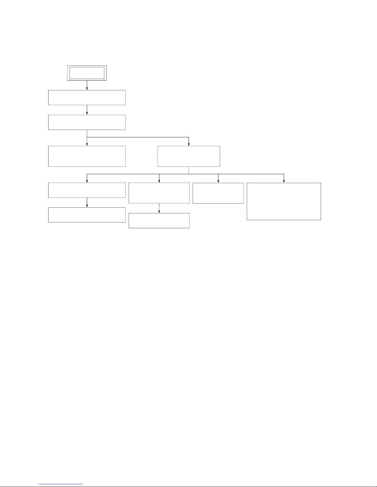
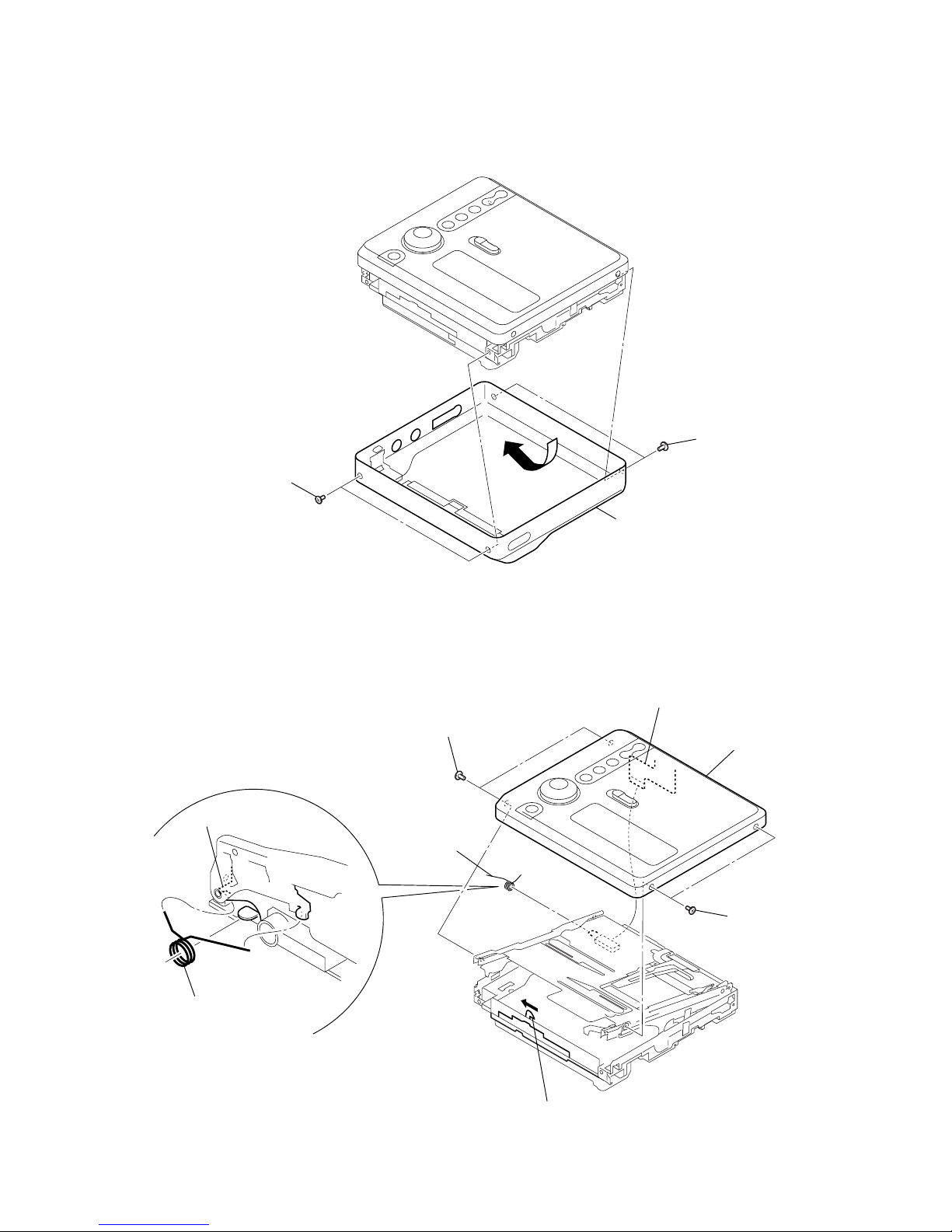
3-2. CASE (LOWER)
(Page 7)
3-3. UPPER PANEL SECTION
(Page 7)
3-4. LCD MODULE,
UPPER PANEL SUB ASSY
(Page 8)
3-5. MECHANISM DECK
(MT-MZN707-177)
(Page 8)
3-6. SET CHASSIS (5192) ASSY
(Page 9)
3-7. MAIN BOARD
(Page 9)
3-8. OP SERVICE ASSY
(LCX-5R)
(Page 10)
3-9. HOLDER ASSY
(Page 11)
3-10. DC MOTOR
(SLED) (M602)
(Page 11)
3-11. DC SSM18B MOTOR
(SPINDLE) (M601),
DC MOTOR (OVER
WRITE HEAD UP/DOWN)
(M603)
(Page 12)
SET
SECTION 3
DISASSEMBLY
• This set can be disassembled in the order shown below.
3-1. DISASSEMBLY FLOW
Page 7
7
MZ-N707
Note: Follow the disassembly procedure in the numerical order given.
3-2. CASE (LOWER)
3-3. UPPER PANEL SECTION
1
two screws
(M1.4)
1
two screws
(M1.4)
2
Remove the case (lower) in th
e
direction of the arrow.
3
two screws
(M1.4)
5
torsion spring
(pop up-L)
3
two screws
(M1.4)
2
Slide the open slider in the direction of the arrow,
and open the upper panel section.
set chassis (5192) assy
torsion spring (pop up-L)
1
flexible board
(CN801)
4
upper panel section
Page 8

8
MZ-N707
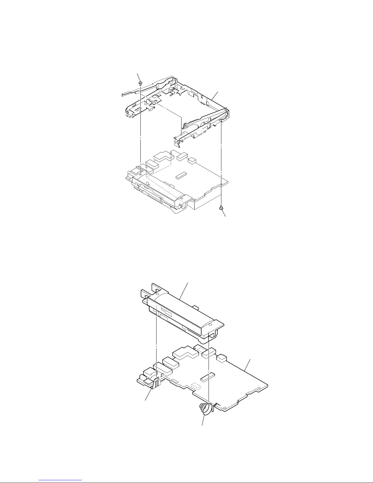
3-4. LCD MODULE, UPPER PANEL SUB ASSY
3-5. MECHANISM DECK (MT-MZN707-177)
1
five screws
(1.7 × 2.5)
2
LCD module
3
compression spring
(button)
Note: On installation, adjust the position of
both switch and knob (hold).
4
button (control A)
knob (hold)
switch
5
upper panel sub ass
y
3
two step screws (MD)
6
mechanism deck
(MT-MZN707-177)
5
flexible board (optical pick-up)
(CN501)
4
2
flexible board (motor)
(CN502)
1
Remove two solders of the
flexible board (over write head).
Page 9
9
MZ-N707
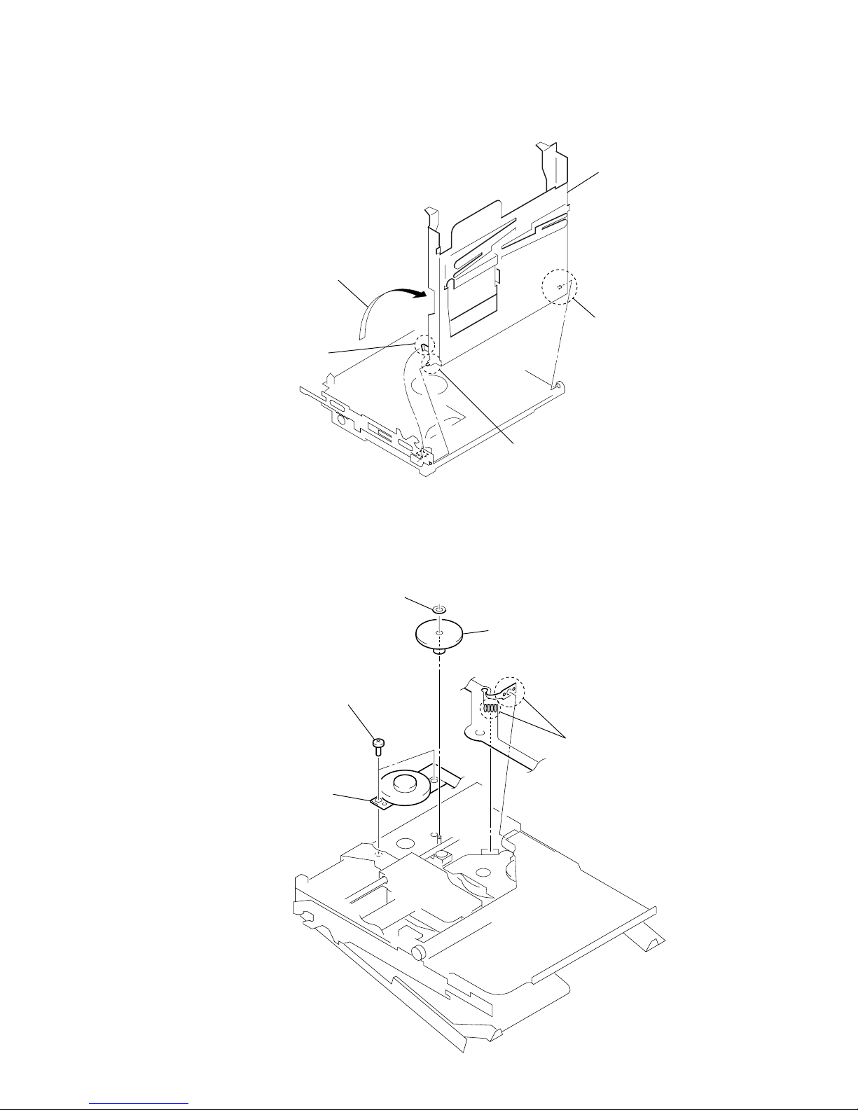
3-6. SET CHASSIS (5192) ASSY
3-7. MAIN BOARD
2
two screws
(1.7 × 2.5)
3
set chassis (5192) assy
1
four screws
(M1.4 × 2)
4
battery case
5
main board
3
battery terminal (–)
2
battery terminal board (+)
Page 10

10
MZ-N707
3-8. OP SERVICE ASSY (LCX-5R)
4
rack spring
3
screw (M1.4)
1
washer (0.8-2.5)
2
gear (SA)
5
screw (M1.4)
6
thrust detent spring
8
Pull off lead screw.
7
over write head section
OP service assy (LCX-5R)
9
Opening the over write head
toward the direction
A
, remove the OP service assy
(LCX-5R) toward the direction
B
.
A
B
Note: Do not open the entire assy forcibly,
when opening the over write head.
Page 11
11
MZ-N707
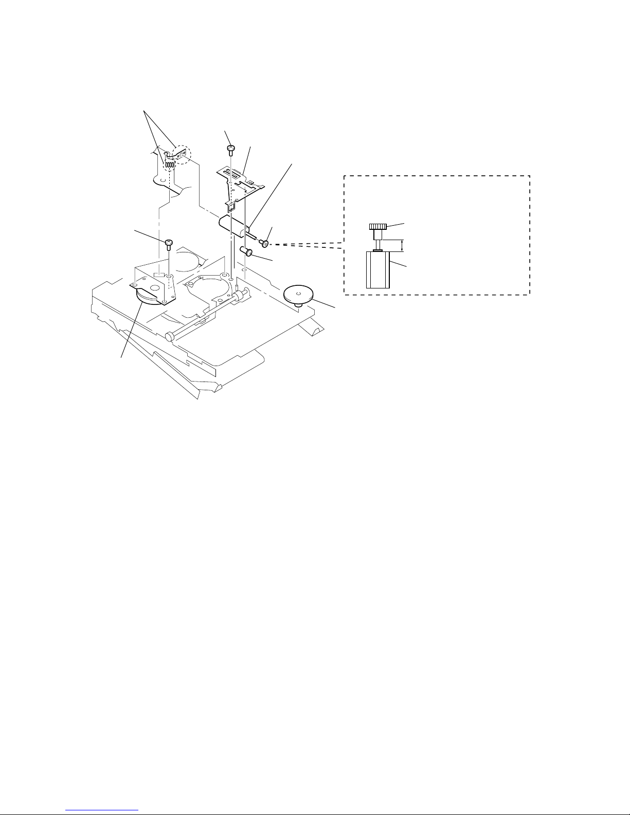
3-9. HOLDER ASSY
3-10. DC MOTOR (SLED) (M602)
4
holder ass
y
3
boss
3
boss
1
convex portion
2
Open the holder assy
2
washer (0.8-2.5)
5
DC motor (sled) (M602)
4
two screws (M1.4)
3
gear (SA)
1
Remove six solders
of the motor flexible board.
Page 12
12
MZ-N707
3-11. DC SSM18B MOTOR (SPINDLE) (M601), DC MOTOR (OVER WRITE HEAD UP/DOWN) (M603)
9
DC SSM18B motor
(spindle) (M601)
8
three tapping screws
2
tapping screw
3
motor cover
6
gear (HA)
4
gear (HB)
5
gear (HC)
DC motor
(over write head up/down)
(M603)
3.15 mm
gear (HA)
Note: Press-fit the gear (HA) up to the position of
the DC motor (over write head up/down)
(M603) as shown below.
7
DC motor (over write head up/down)
(M603)
1
Remove six solders of the
motor flexible board.
Page 13
13
MZ-N707
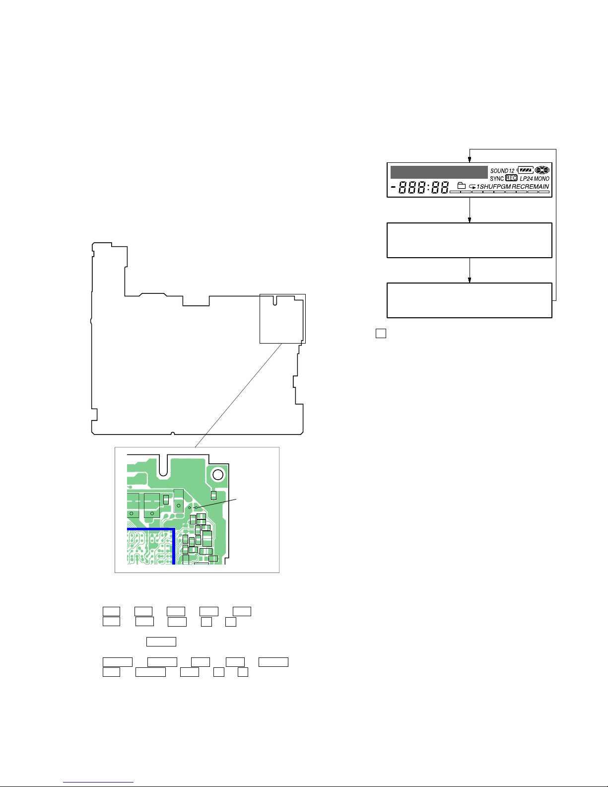
OPERATION IN SETTING THE TEST MODE
• When the test mode becomes active, first the display check mode
is selected.
• Other mode can be selected from the display check mode.
• When the test mode is set, the LCD repeats the following dis-
play.
2 In the normal mode, turn on the [HOLD] switch. While press-
ing the [VOL --] key press the following order:
> t > t . t . t > t
. t > t . t X t X
3 In the normal mode, turn on the [HOLD] switch. While
pressing the x/CHG key, press the keys on the remote
commander with the following order:
N > t N > t . t . t N > t
. t N > t . t X t X
Note: If electrical adjustment (CD and MO overall adjustment) has not
been finished completely , “NV Error” is displayed on LCDs of the
set and the remote commander.
SECTION 4
TEST MODE
OUTLINE
• This set provides the Overall adjustment mode that allows CD
and MO discs to be automatically adjusted when in the test mode.
In this overall adjustment mode, the disc is discriminate between
CD and MO, and each adjustment is automatically executed in
order. If a fault is found, the system displays its location. Also,
the manual mode allows each individual adjustment to be automatically adjusted.
• Operation in the test mode is performed with the set. A key
having no particular description in the text, indicates a set key.
SETTING METHOD OF TEST MODE
There are three different methods to set the test mode:
1 Short SL801 (TEST) on the MAIN board with a solder bridge
(connect pin <zvn of IC801 to the ground). Then, turn on the power .
827
C839
R817
C814
FB801
R821
R823
R824
R858
R825
C822
C816
R822
R857
C817
C809
+
C815
+
C821
+
195
199
178
174
170
203
180
176
172
175
171
169
197
193
191
189
185
187
173
179
177
183
182
207
181
184
186
215
188
209
190
211
213
192
194
1
7
0
4
9
8
9
6
SL801
(TEST)
C625
SL801
(TEST)
– MAIN Board (Conductor Side) –
Microcomputer
version
display
All off
All lit
Set LCD display
Ver 1.100
00 3
• When the X key is pressed and hold down, the display at that
time is held so that display can be checked.
RELEASING THE TEST MODE
For test mode set with the method 1:
Turn off the power and open the solder bridge on SL801 (TEST)
on the MAIN board.
Note: Remove the solders completely. Remaining could be shorted with
the chassis, etc.
For test mode set with the method 2 or 3:
Turn off the power.
Page 14

14
MZ-N707
CONFIGURATION OF TEST MODE
MANUAL MODE
Mode to adjust or check the operation of the set by function.
Normally, the adjustment in this mode is not executed.
However, the Manual mode is used to clear the memory, power
supply adjustment, and laser power check before performing
automatic adjustments in the Overall Adjustment mode.
• Transition Method in Manual Mode
1. Set the test mode (see page 13).
2. Press the > or[VOL +] key activates the manual mode where
the LCD display as shown below.
3. During each test, the optical pick-up moves outward or inward while the
> or . key is pressed for several sec-
onds respectively.
4. Each test item is assigned with a 3-digit item number;
100th place is a major item, 10th place is a medium item, and
unit place is a minor item.
The values adjusted in the test mode are written to the
nonvolatile memory (for the items where adjustment was
made).
Press the x/CHG key
[Manual Mode]
[Servo Adjustment]
[Audio Adjustment]
[Power Supply Adjustment]
[OP Alignment Adjustment]
[Overall Adjustment Mode]
[Sound Skip Check Result Display Mode]
[Key Check Mode]
[Test Mode $Display Check Mode%]
Press the x/CHG key
Press the . or [VOL --] key
Press the N or [REC] key
Press the > or [VOL +] key
[Electrical Offset Adjustment]
Power Supply Adjustment
Auto Item Feed
CD Overall Adjustment/
MO Overall Adjustment
[Self-Diagnosis Result Display Mode]
Press the [MENU] key
Press the
[T MARK] key
The key check quits, or open the upper panel
Press the
x/CHG key
Press the x/CHG key
x/CHG
key
x/CHG
key
[VOL +]
key: 100th place of item number
increase.
[VOL --]
key: 100th place of item number
decrease.
[Major item switching]
[VOL +]
key: 10th place of item number
increase.
[VOL --]
key: 10th place of item number
decrease.
[VOL +]
key: Increases the adjusted
value of the 1st digit
[VOL --]
key: Decreases the adjusted
value of the 1st digit
[Medium item switching]
N
key
N
key
[Minor item switching]
[Adjusted value variation]
X
key: When adjusted value is
changed:
Adjusted value is written.
When adjusted value is
not changed:
That item is adjusted
automatically.
[Adjusted value write]
>
key: Unit place of item number
increase.
.
key:Unit place of item number
decrease.
Manual
0 00
Set LCD display
Page 15

15
MZ-N707
5. The display changes a shown below each time the
[MENU] key is pressed.
However in the power mode (item number 700’s), only the
item is displayed.
6. Quit the manual mode, and press the
x/CHG key to return to
the test mode (display check mode).
OVERALL ADJUSTMENT MODE
Mode to adjust the servo automatically in all items.
Normally, automatic adjustment is executed in this mode at the
repair.
For further information, refer to “SECTION 5 ELECTRICAL
ADJUSTMENTS” (see page 19).
item number
address adjusted value
• Address & Adjusted Value Display
Set LCD display
• Jitter Value & Adjusted Value Display
Set LCD display
• Block Error Value & Adjusted Value Display
Set LCD display
• ADIP Error Value & Adjusted Value Display
Set LCD display
• Focus Drive Value & Adjusted Value Display
Set LCD display
• Item Title Display
Set LCD display
C68S1B
0 11
item number
jitter value adjusted value
0FEJ1B
0 11
item number
block error value adjusted value
063B1B
0 11
item number
ADIP error value adjusted value
081A1B
0 11
item number
Focus drive value adjusted value
000F1B
0 11
item number
item title adjusted value
LrefPw 1B
0 11
SELF-DIAGNOSIS RESULT DISPLAY MODE
This set uses the self-diagnostic function system in which if an
error occurred during the recording or playing, the mechanism
control block and the power supply control block in the
microcomputer detect it and record its cause as history in the
nonvolatile memory.
By checking this history in the test mode, you can analyze a fault
and determine its location.
Total recording time is recorded as a guideline of how long the
optical pickup has been used, and by comparing it with the total
recording time at the time when an error occurred in the selfdiagnosis result display mode, you can determine when the error
occurred.
Clear both self-diagnosis history data and total recording time, if
the optical pickup was replaced.
• Self-Diagnosis Result Display Mode Setting Method
1. Set the test mode (see page 13).
2. In the display check mode, press the [MENU] key activates the
self-diagnosis result display mode where the LCD display as
shown below.
3. Then, each time the
> key is pressed, LCD display descends
by one as shown below. Also, the LCD display ascends by one
when the . key is pressed.
If the
[MENU] key is pressed with this display, the LCD switches
to the simple display mode.
4. Quit the self-diagnosis result display mode, and press the x/
CHG key to return to the test mode (display check mode).
1 ****
0 XX
N ****
0 XX
N1****
0 XX
N2****
0 XX
R_****
0 XX
1
1
XX
: Error code
****
: Total recording time
1 0000
0 XX
history code
error display code
Total recording time
when error occurred
Set LCD display
Page 16

16
MZ-N707
• Description of Indication History
History code number Description
1 The first error
N The last error
N1 One error before the last.
N2 Two errors before the last.
R_ Total recording time
RESET THE ERROR DISPLAY CODE
After servicing, reset the error display code.
• Setting Method of Reset the Error Display Code
1. Set the test mode (see page 13).
2. Press the [MENU] key activates the self-diagnosis result display
mode.
3. To reset the error display code, press the X key (twice) when
the code is displayed (except “R_****”).
(All the data on the 1, N, N1, and N2 will be reset)
• Description of Error Indication Codes
Problem Indication code Meaning of code Simple display Description
No error 00 No error --- No error
01
Illegal access target
Adrs Attempt to access an abnormal address
address was specified
Servo system error 02 High temperature Temp High temperature detected
03 Focus error Fcus Disordered focus or can not read an address
04 Spindle error Spdl Abnormal rotation of disc
TOC error
11 TOC error TOC Faulty TOC contents
12 Data reading error Data Data could not be read at SYNC
Power supply system error 22 Low battery LBat Momentary interruption detected
31 Offset error Ofst Offset error
32
Focus error ABCD
ABCD Focus error ABCD offset error
offset error
Offset system error
33
Tracking error
TE Tracking error Offset error
Offset error
34
X1 tracking error
X1TE X1 tracking error Offset error
Offset error
Disc error 35
MD DATA 2
MD2 MD DATA 2 disc error
disc error
Page 17
17
MZ-N707
• Cause of Sound Skip Error
Cause of error Description of error
EIB Sound error correction error
Play
Stat Decoder status error
Adrs Address access error
BEmp Buffer is empty
BOvr
Buffer is full, and sounds were
dumped
Record
Bful
Buffer capacity becomes less,
and forcible writing occurred
Rtry Retry times over
4. To quit the sound skip check result display mode and to return
to the test mode (display check mode), press the x/CHG key.
• Setting Method of Key Check Mode
1. Set the test mode (see page 13).
2. Press the [T MARK] key activates the key check mode.
3. When each key on the set and on remote commander is pressed,
its name is displayed on the remote commander LCD. (The
operated position is displayed for 4 seconds after the slide
switch is operated. If any other key is pressed during this display, the remote commander LCD switches to its name display)
Example1: When the > key on the set is pressed:
Example2: When the N > key on the remote commander
is pressed:
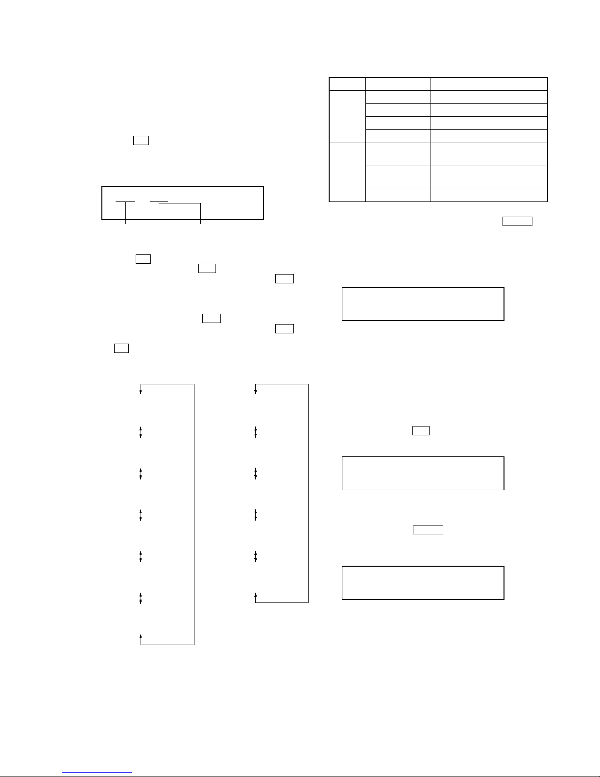
SOUND SKIP CHECK RESULT DISPLAY MODE
This set can display the count of errors that occurred during the
recording/playing for checking.
• Setting Method of Sound Skip Check Result Display
Mode
1. Set the test mode (see page 13).
2. Press the N key or [REC] ke y, and the playing or recording
sound skip result display mode becomes active respectively
where the LCD displays the following.
3. When the
N key is pressed, total error count is displayed on
the LCD, and each time the > key is pressed, the display
item moves down by one as sho wn below . Also, if the . key
is pressed, the display item moves up by one, then if the [REC]
key is pressed, the display in the record mode appears.
When the [REC] key is pressed, total error count is displayed
on the LCD, and each time the > key is pressed, the display
item moves down by one as sho wn below . Also, if the . key
is pressed, the display item moves up by one, then if
the N key is pressed, the display in the play mode appears.
P**R**
0 00
EIB **
0 00
Stat**
0 00
Adrs**
0 00
BEmp**
0 00
######
0 00
P**R**
0 00
BOvr**
0 00
Bful**
0 00
Rtry**
0 00
######
0 00
P**R**
: Total play/record errors (hex.)
**
: Counter of sound skip check each item (hex.)
######
: 6-digit address where sound was skipped last (hex.)
Playing sound skip
result display
Recording sound skip
result display
**
0 04
**
: AD value of the remote commander key
(hexadecimal 00 to FF)
Set LCD display
FF **
0 04
**
: AD value of the remote commander key
(hexadecimal 00 to FF)
Set LCD display
rPLAY **
0 04
**
: AD value of the remote commander key
(hexadecimal 00 to FF)
Set LCD display
P**R**
0 00
Total count of play
system errors (hex.)
Total count of record
system errors (hex.)
Set LCD display
Page 18

18
MZ-N707
4. When all the keys on the set and on the remote commander are
considered as OK, the following displays are shown for 4 seconds.
Example1: When the keys on the set are considered as OK:
Example2: When the keys on the remote commander are con-
sidered as OK:
5. When all keys were checked or if the upper panel is opened,
the key check mode quits and the test mode (display check
mode) comes back.
SET OK **
8 88
**
: AD value of the remote commander key
(hexadecimal 00 to FF)
Set LCD display
RMC OK **
8 88
**
: AD value of the remote commander key
(hexadecimal 00 to FF)
Set LCD display
Page 19
19
MZ-N707
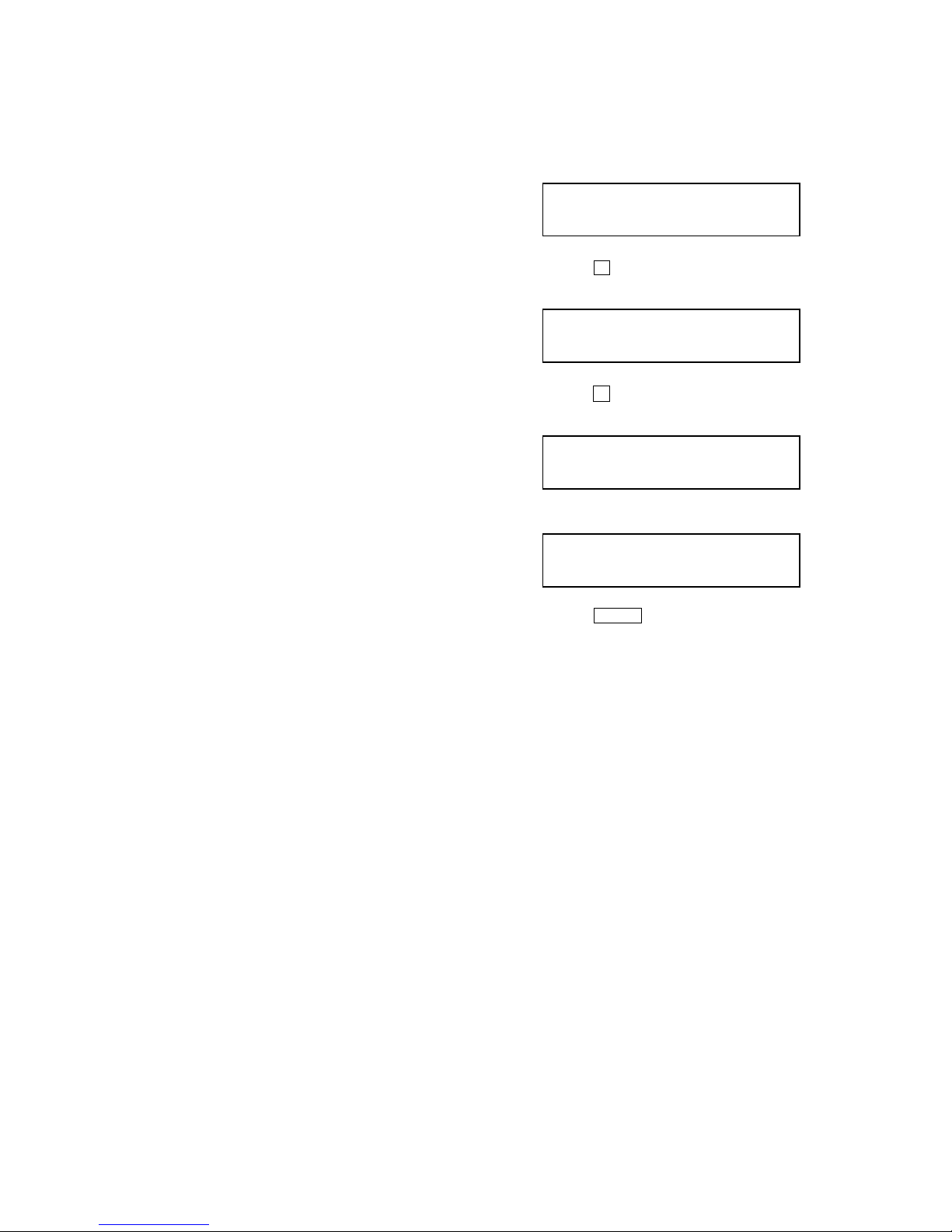
• Setting Method of NV Reset
1. Select the manual mode of the test mode, and set item number
021 NV Reset (see page 14).
2. Press the X key.
3. Press the X key once more.
4. Press the x/CHG key to quit the manual mode, and return
the test mode (display check mode).
• Change of NV Adjusted Values (Version 1.100)
Caution: Change the NV adjustment values according to the mi-
crocomputer version.
In this set, some adjusted values were set in the manual mode at
the shipment, but these will be cleared when the NV is reset.
Therefore, modify the NV adjusted values through the following
procedure immediately after the NV was reset.
1. Item numbers in which the NV adjusted values are to be modi-
fied
– Change ABCD gain [Hpit] initial value (item number 336)
Caution: The ABCD gain [Hpit] initial value must be
changed before the overall adjustment.
– Change BatFlg value (item number 741)
– Change NiRec0 to 4 values (item numbers 771 to 775)
– Change NiPb 0 to 4 values (item numbers 776 to 779, 781)
– Change CL V dri ve voltage limiter (item n umbers 865, 866)
– Change x2 CL V speed gain, +6dB compared to con ventional
(item numbers 867, 868)
– Change x2 CL V phase gain, +3dB compared to con ventional
(item numbers 871, 872)
– Change x2/x1 switching temperature threshold value
(+10°C t +5°C) (item numbers 873, 874)
ResOK?
0 21
Set LCD display
SECTION 5
ELECTRICAL ADJUSTMENTS
Res***
0 21
Set LCD display
Reset!
0 21
r
NV reset (after several seconds)
OUTLINE
• In this set, automatic adjustment of CD and MO can be performed by entering the test mode.
However, before starting automatic adjustment, the memory
clear, power supply adjustment, and laser power check must be
performed in the manual mode.
• A key having no particular description in the text, indicates a
set key.
PRECAUTIONS FOR ADJUSTMENT
1. Adjustment must be done in the test mode only.
After adjusting, release the test mode.
2. Use the following tools and measuring instruments.
• Test CD disc TDYS-1
(Part No. : 4-963-646-01)
• SONY MO disc available on the market
• Digital voltmeter
• Laser power meter LPM-8001
(Part No. : J-2501-046-A)
• Thermometer (using the Temperature Correction)
3. Unless specified otherwise, supply DC 3V from the DC IN
3V jack (J601).
4. Switch position
HOLD switch ............................................... ON
ADJUSTMENT SEQUENCE
1. NV Reset (EEPROM clear)
Manual Mode
r
2. Power Supply Manual Adjustment
Manual Mode
r
3. Temperature Correction (item number: 015)
r
Manual Mode
4. Laser Power Check
r
5. Electrical Offset Adjustment
Caution: This adjustment must be made with
no disc loaded.
r Overall Mode
6. CD Overall Adjustment
r
7. MO Overall Adjustment
r
Manual Mode
8. RESUME Clear
Note: If the version of the microcomputer is 1.000 or later, “3. T empera-
ture Correction” and “2. Power Supply Manual Adjustment” can
be performed continuously in reverse order with pressing the [END
SEARCH]
key in the overall adjustment mode.
NV RESET
Caution: The shipment data will be cleared when the NV is reset.
Therefore, change the NV adjusted values following the
Change of NV Adjusted Values immediately after the
NV was reset.
Change the NV adjustment values according to the microcomputer version.
ResNV CC
0 21
Set LCD display
Page 20
20
MZ-N707
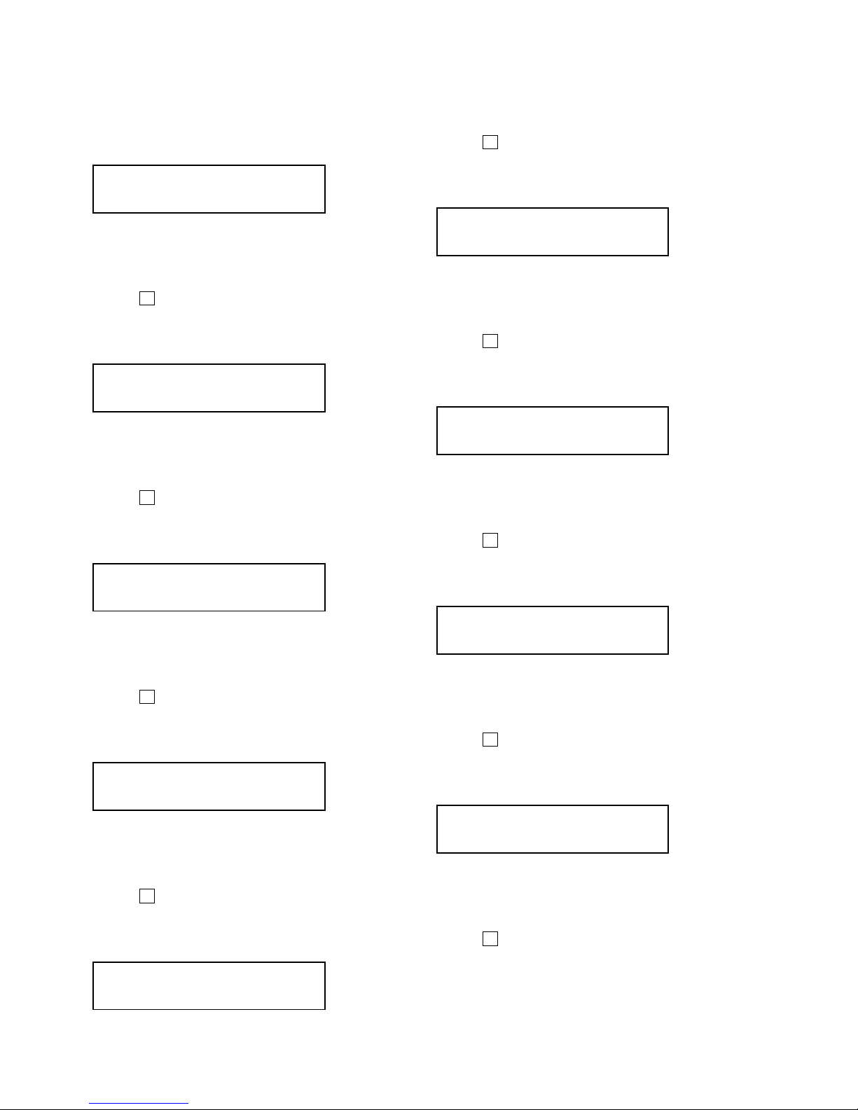
2. NV adjusted values modifying procedure
1) Select manual mode of the test mode, and set item number
336 (see page 14).
2) Adjust with the [VOL +] key (adjusted value up) or [VOL --]
key (adjusted value down) so that the adjusted value becomes
08.
3) Press the X key to write the adjusted value.
4) Select manual mode of the test mode, and set item number
741 (see page 14).
5) Adjust with the [VOL +] key (adjusted value up) or [VOL --]
key (adjusted value down) so that the adjusted value becomes
02.
6) Press the X key to write the adjusted value.
7) Select manual mode of the test mode, and set item number
771 (see page 14).
8) Adjust with the
[VOL +] key (adjusted value up) or [VOL --]
key (adjusted value down) so that the adjusted value becomes
6E.
9) Press the X key to write the adjusted value.
10) Select manual mode of the test mode, and set item number
772 (see page 14).
11) Adjust with the [VOL +] key (adjusted value up) or [VOL --]
key (adjusted value down) so that the adjusted value becomes
7C.
12) Press the X key to write the adjusted value.
13) Select manual mode of the test mode, and set item number
773 (see page 14).
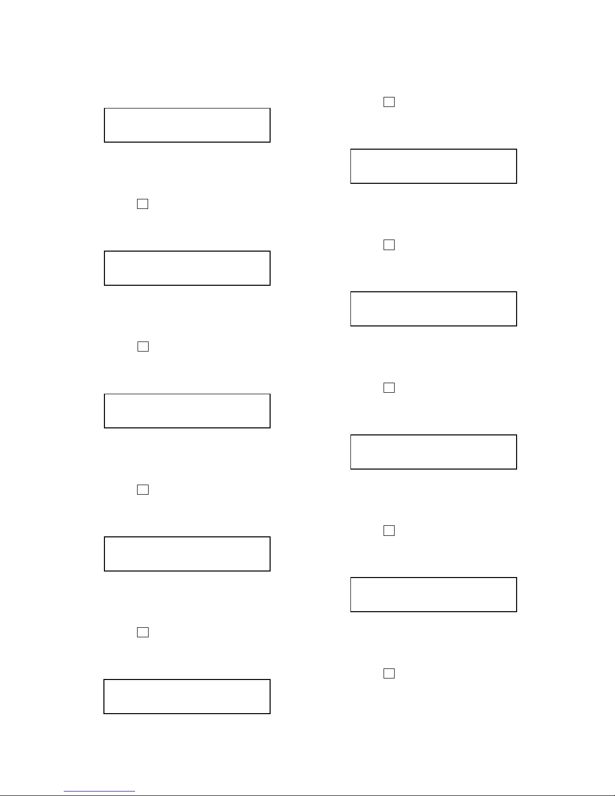
AbcdGn **
3 36
**
: Adjusted value
Set LCD display
BatFlg **
7 41
**
: Adjusted value
Set LCD display
NiRec0 **
7 71
**
: Adjusted value
Set LCD display
NiRec1 **
7 72
**
: Adjusted value
Set LCD display
NiRec2 **
7 73
**
: Adjusted value
Set LCD display
14) Adjust with the [VOL +] key (adjusted value up) or [VOL --]
key (adjusted value down) so tha t the adjusted value becomes
7D.
15) Press the X key to write the adjusted value.
16) Select manual mode of the test mode, and set item number
774 (see page 14).
17) Adjust with the [VOL +] key (adjusted value up) or [VOL --]
key (adjusted value down) so tha t the adjusted value becomes
7F.
18) Press the X key to write the adjusted value.
19) Select manual mode of the test mode, and set item number
775 (see page 14).
20) Adjust with the [VOL +] key (adjusted value up) or [VOL--]
key (adjusted value down) so tha t the adjusted value becomes
81.
21) Press the X key to write the adjusted value.
22) Select manual mode of the test mode, and set item number
776 (see page 14).
23) Adjust with the
[VOL +] key (adjusted value up) or [VOL --]
key (adjusted value down) so tha t the adjusted value becomes
5B.
24) Press the X key to write the adjusted value.
25) Select manual mode of the test mode, and set item number
777 (see page 14).
26) Adjust with the [VOL +] key (adjusted value up) or [VOL --]
key (adjusted value down) so tha t the adjusted value becomes
7B.
27) Press the X key to write the adjusted value.
NiRec3 **
7 74
**
: Adjusted value
Set LCD display
NiRec4 **
7 75
**
: Adjusted value
Set LCD display
NiPb 0 **
7 76
**
: Adjusted value
Set LCD display
NiPb 1 **
7 77
**
: Adjusted value
Set LCD display
Page 21
21
MZ-N707
41) Adjust with the [VOL +] key (adjusted value up) or [VOL --]
key (adjusted value down) so that the adjusted value becomes
B9.
42) Press the X key to write the adjusted value.
43) Select manual mode of the test mode, and set item number
867 (see page 14).
44) Adjust with the [VOL +] key (adjusted value up) or [VOL --]
key (adjusted value down) so that the adjusted value becomes
C9.
45) Press the X key to write the adjusted value.
46) Select manual mode of the test mode, and set item number
868 (see page 14).
47) Adjust with the [VOL +] key (adjusted value up) or [VOL --]
key (adjusted value down) so that the adjusted value becomes
80.
48) Press the X key to write the adjusted value.
49) Select manual mode of the test mode, and set item number
871 (see page 14).
50) Adjust with the
[VOL +] key (adjusted value up) or [VOL--]
key (adjusted value down) so that the adjusted value becomes
CA.
51) Press the X key to write the adjusted value.
52) Select manual mode of the test mode, and set item number
872 (see page 14).
53) Adjust with the [VOL +] key (adjusted value up) or [VOL --]
key (adjusted value down) so that the adjusted value becomes
2D.
54) Press the X key to write the adjusted value.
28) Select manual mode of the test mode, and set item number
778 (see page 14).
29) Adjust with the
[VOL +] key (adjusted value up) or [VOL --]
key (adjusted value down) so tha t the adjusted value becomes
7D.
30) Press the X key to write the adjusted value.
31) Select manual mode of the test mode, and set item number
779 (see page 14).
32) Adjust with the [VOL +] key (adjusted value up) or [VOL --]
key (adjusted value down) so tha t the adjusted value becomes
7F.
33) Press the X key to write the adjusted value.
34) Select manual mode of the test mode, and set item number
781 (see page 14).
35) Adjust with the
[VOL +] key (adjusted value up) or [VOL --]
key (adjusted value down) so tha t the adjusted value becomes
81.
36) Press the X key to write the adjusted value.
37) Select manual mode of the test mode, and set item number
865 (see page 14).
38) Adjust with the [VOL +] key (adjusted value up) or [VOL --]
key (adjusted value down) so tha t the adjusted value becomes
2C.
39) Press the X key to write the adjusted value.
40) Select manual mode of the test mode, and set item number
866 (see page 14).
NiPb 2 **
7 78
**
: Adjusted value
Set LCD display
NiPb 3 **
7 79
**
: Adjusted value
Set LCD display
NiPb 4 **
7 81
**
: Adjusted value
Set LCD display
V3 dat **
8 66
**
: Adjusted value
Set LCD display
V4 num **
8 67
**
: Adjusted value
Set LCD display
V4 dat **
8 68
**
: Adjusted value
Set LCD display
V3 num **
8 65
**
: Adjusted value
Set LCD display
V5 num **
8 71
**
: Adjusted value
Set LCD display
V5 dat **
8 72
**
: Adjusted value
Set LCD display
Page 22
22
MZ-N707
POWER SUPPLY MANUAL ADJUSTMENT
• Adjustment Sequence
Adjustment must be done with the following steps.
1. Vc PWM Duty (L) adjustment (item number: 762)
r
2. Vc PWM Duty (H) adjustment (item number: 763)
r
3. Vl PWM Duty (L) adjustment (item number: 764)
r
4. Vl PWM Duty (H) adjustment (item number: 765)
r
5. Vrec PWM Duty (L) adjustment (item number: 766)
r
6. Vrec PWM Duty (H) adjustment (item number: 767)
• Setting Method of Power Supply Manual Adjustment
1. Make sure that the power supply voltage is 3V.
2. Select the manual mode of the test mode (see page 14).
3. Set item number.
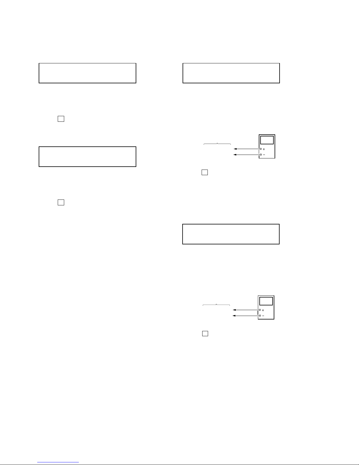
• Adjustment Method of Vc PWM Duty (L)
(item number: 762)
1. Connect a digital voltmeter to the AP912 (VCO) on the MAIN
board, and adjust
[VOL +] key (voltage up) or [VOL --] key (volt-
age down) so that the voltage becomes 2.40 ± 0.05 V.
2. Press the X key to write the adjusted value.
Adjustment and Connection Location:MAIN board
(see page 25)
• Adjustment Method of Vc PWM Duty (H)
(item number: 763)
1. Connect a digital voltmeter to the AP912 (VCO) on the MAIN
board, and adjust
[VOL +] key (voltage up) or [VOL --] key
(voltage down) so that the voltage becomes 2.75 ± 0.05 V.
2. Press the X key to write the adjusted value.
Adjustment and Connection Location:MAIN board
(see page 25)
digital
voltmete
r
MAIN board
AP912 (VCO)
AP602 (GND)
digital
voltmete
r
MAIN board
AP912 (VCO)
AP602 (GND)
VclPWM **
7 62
**
: Adjusted value
Set LCD display
VchPWM **
7 63
**
: Adjusted value
Set LCD display
55) Select manual mode of the test mode, and set item number
873 (see page 14).
56) Adjust with the [VOL +] key (adjusted value up) or [VOL --]
key (adjusted value down) so that the adjusted value becomes
BB.
57) Press the X key to write the adjusted value.
58) Select manual mode of the test mode, and set item number
874 (see page 14).
59) Adjust with the [VOL +] key (adjusted value up) or [VOL --]
key (adjusted value down) so that the adjusted value becomes
05.
60) Press the X key to write the adjusted value.
V6 num **
8 73
**
: Adjusted value
Set LCD display
V6 dat **
8 74
**
: Adjusted value
Set LCD display
Page 23
23
MZ-N707
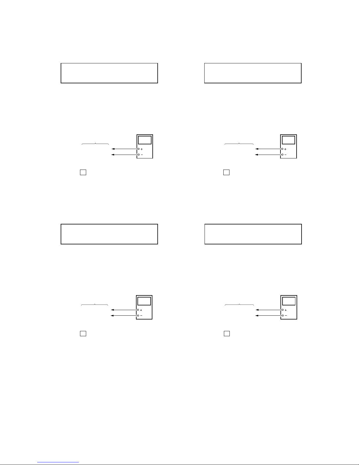
• Adjustment Method of Vl PWM Duty (L)
(item number: 764)
1. Connect a digital voltmeter to the AP913 (VLO) on the MAIN
board, and adjust [VOL +] key (voltage up) or [VOL --] key
(voltage down) so that the voltage becomes 2.30 ± 0.01 V.
2. Press the X key to write the adjusted value.
Adjustment and Connection Location:MAIN board
(see page 25)
• Adjustment Method of Vl PWM Duty (H)
(item number: 765)
1. Connect a digital voltmeter to the AP913 (VLO) on the MAIN
board, and adjust
[VOL +] key (voltage up) or [VOL --] key
(voltage down) so that the voltage becomes 2.55 ± 0.01 V.
2. Press the X key to write the adjusted value.
Adjustment and Connection Location:MAIN board
(see page 25)
digital
voltmete
r
MAIN board
AP913 (VLO)
AP602 (GND)
VLpwmL **
7 64
**
: Adjusted value
Set LCD display
digital
voltmete
r
MAIN board
AP913 (VLO)
AP602 (GND)
VLpwmH **
7 65
**
: Adjusted value
Set LCD display
• Adjustment Method of Vrec PWM Duty (L)
(item number: 766)
1. Connect a digital voltmeter to the TP (VREC) on the MAIN
board, and adjust [VOL +] key (voltage up) or [VOL --] key
(voltage down) so that the voltage becomes 1.13 ± 0.02 V.
2. Press the X key to write the adjusted value.
Adjustment and Connection Location:MAIN board
(see page 25)
• Adjustment Method of Vrec PWM Duty (H)
(item number: 767)
1. Connect a digital voltmeter to the TP (VREC) on the MAIN
board, and adjust
[VOL +] key (voltage up) or [VOL --] key
(voltage down) so that the voltage becomes 1.65 to 1.75 V.
2. Press the X key to write the adjusted value.
Adjustment and Connection Location:MAIN board
(see page 25)
digital
voltmete
r
MAIN board
TP (VREC)
AP602 (GND)
RECpwL **
7 66
**
: Adjusted value
Set LCD display
digital
voltmete
r
MAIN board
TP (VREC)
AP602 (GND)
RECpwH **
7 67
**
: Adjusted value
Set LCD display
Page 24
24
MZ-N707
TEMPERATURE CORRECTION
• Adjustment Method of Temperature Correction
1. Select the manual mode of test mode, and set the item number
015 (see page 14).
2. Measure the ambient temperature.
3. Adjust with [VOL +], [VOL --] key so that the adjusted value
(hexadecimal value) becomes the ambient temperature.
(Initial value: 19h = 25 °C, Adjusting range: 80h to 7fh (–128
°C to +127 °C)
4. Press the X key to write the adjusted value.
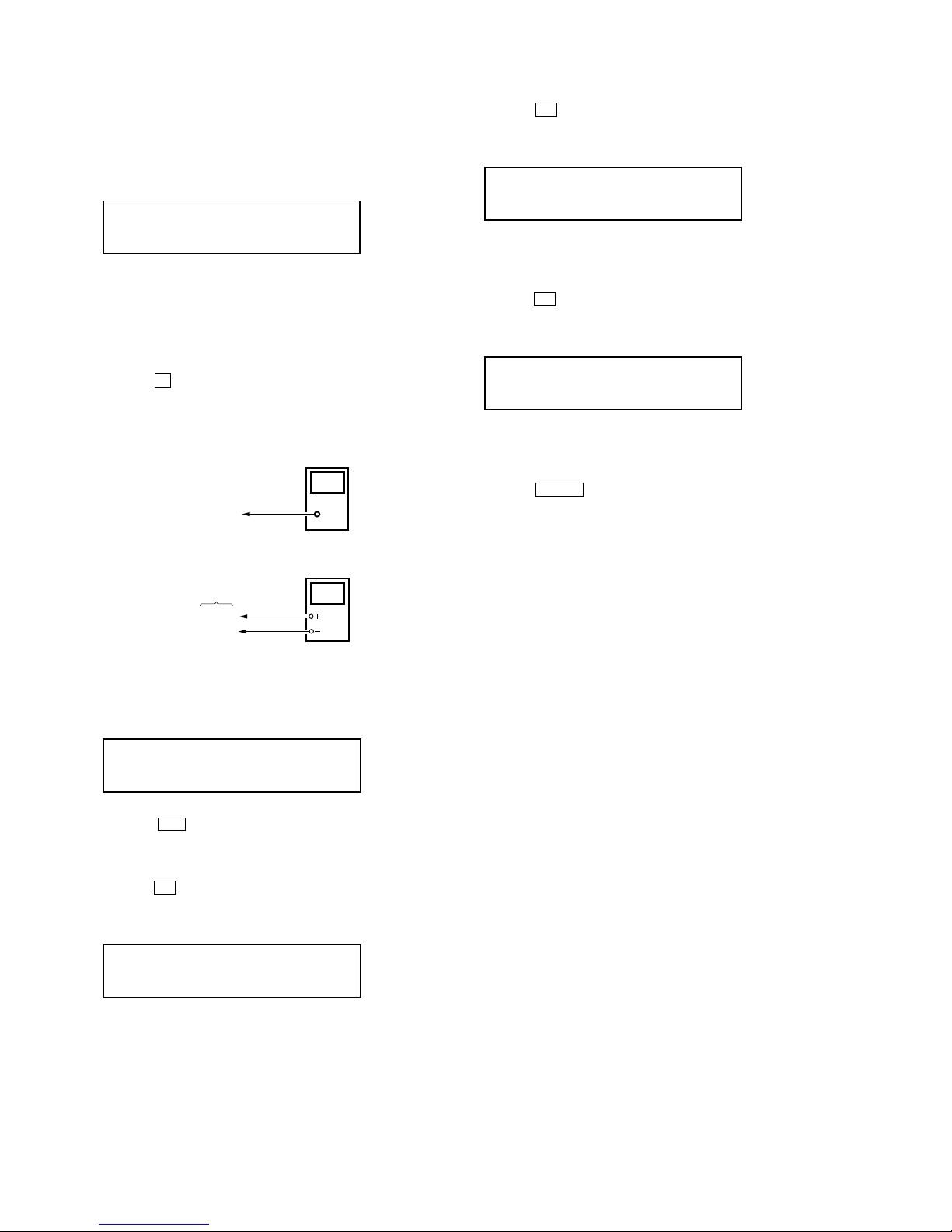
LASER POWER CHECK
• Connection
• Checking Method
1. Select the manual mode of test mode (see page 14), and set
the laser power adjusting mode (item number 010).
2. Press the
. key continuously until the optical pick-up
moves to the most inward track.
3. Open the cover and set the laser power meter on the objectiv e
lens of the optical pick-up.
4. Press the N key , and set the laser MO read adjustment mode
(item number 011).
5. Check that the laser power meter reading is 0.81 ± 0.08 mW.
6. Check that the voltage both ends (TP (+) and TP (–)) of resistor R521 at this time is below 44 mV.
7. Press the
N key, and set the laser CD read adjustment mode
(item number 012).
8. Check that the laser power meter reading is 0.97 ± 0.10 mW.
9. Check that the voltage both ends (TP (+) and TP (–)) of resistor R521 at this time is below 44 mV.
10. Press the N key , and set the laser MO write adjustment mode
(item number 013).
11. Check that the laser power meter reading is 4.95 ± 0.50 mW.
12. Check that the voltage both ends (TP (+) and TP (–)) of resistor R521 at this time is below 80 mV.
13. Press the x/CHG key to quit the manual mode, and activate
the test mode (display check mode).
Checking and Connection Location: MAIN board
(see page 25)
digital voltmeter
MAIN board
laser
power meter
Optical pick-up
objective lens
TP (+)
TP (–)
Laser
0 10
Set LCD display
LrefPw **
0 11
Set LCD display
HrefPw **
0 12
Set LCD display
SetTmp **
0 15
**
: Adjusted value
Set LCD display
WritPw **
0 13
Set LCD display
Page 25
25
MZ-N707
C914
C513
C527
C514
C523
C910
C909
C915
C917
R946
C912
R920
R615
R906
R626
R604
R605
C506
C507
R505
R517
C504C530
R916
R921
R948
R908
R907
C924
C928
R927
C515
C516
R911
R624
859
C824
C805
R861
R804
R836
C639
R621
R606
R622
R608
C607
C633
R620
C613 C614
R612
C629
C621
R614
R613
C619
C616
C618
R826
C804
R852
R864
R810
C826
C838
R801
C802
R834
R835
R843
FB806
C832 C833 R838
R
529
+
24
+
C901
+
C902
+
C911
+
C919
+
C926
+
C603
+
C622
+
L602
L801
C609
+
C632
+
D901
A
D606
AK
D608
KA
ECB
Q901
IC901
14
56
43
942
IC501
22 23
Q904
B
C
E
Q602
Q605
114
15
28
56
43
2942
IC601
14
85
Q604
58
41
X802
Q801
B1
B2
E
C1
C2
*
IC801
143
139
147
130
128
124
120
103
142
138
134
137
126
122
151
140
131
133
123
125
135
105
107
109
111
141
113
136
132
129
119
121
127
115
118
117
99
101
116
96
97
114
112
93
91
108
110
87
89
104
106
83
85
100
102
79
75
94
98
81
76
92
95
77
78
88
90
59
74
84
86
57
65
80
82
72
67
63
61
10
41
45
49
53
55
71
69
39
43
47
51
54
707366
68
15
14
44
48
52
58
62
64
22
20
42
46
50
56
60
2
14
85
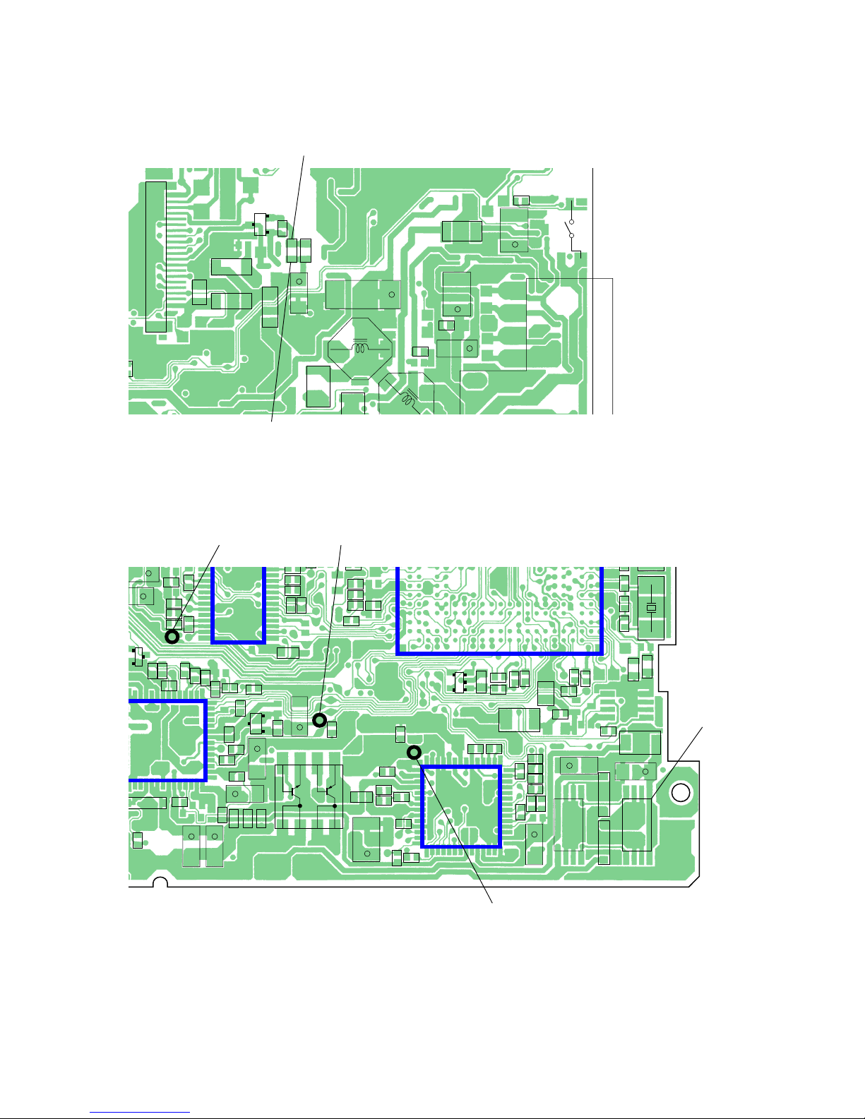
AP602
(GND)
AP913 (VLO) AP912 (VCO)
AP602 (GND)
TP (VREC)
C803
R853
L902
L901
C913
R105
F801
C204
+
C104
+
C316
+
C630
+
L905
06
L502
L501
L904
R521
R522
C518
R519
C904
+
CN501
1
20
Q501
E
C
B
S806
(OPEN/CLOSE DETECT)
J302
TP (−)
TP (+)
– MAIN Board (Component Side) –
– MAIN Board (Conductor Side) –
Adjustment/checking and Connection Location:
Page 26
26
MZ-N707
Note: Adjust the CD first, when performing adjustment.
• Electrical Offset Adjusting Method
Caution: The electrical offset adjustment must be made with no
disc loaded.
1. Make sure that the power supply voltage is 3 V.
2. Set the test mode (see page 13).
3. Press the . or [VOL --] key to activate the overall adjustment
mode.
4. Press the [MENU] key.
5. Electrical offset adjustment is over, if the following display
appears.
x/CHG key
> key
. key
Overall adjustment mode
(Title display)
CD overall
adjusting
CD overall
adjustment
OK
MO overall
adjusting
MO overall
adjustment
OK
CD overall
adjustment
NG
MO overall
adjustment
NG
All item
OK
Protect switch
ON
Protect switch
OFF
[MENU] key
NG item exists
or
NG item exists
or
x/CHG key
[END SEARCH] key
[Test mode $display check mode%]
N key
N key
Electrical
offset
adjustment
Temperature
correction
and
Power supply
adjustment
auto item feed
x/CHG key
x/CHG key
x/CHG key
x/CHG key
x/CHG key
x/CHG key
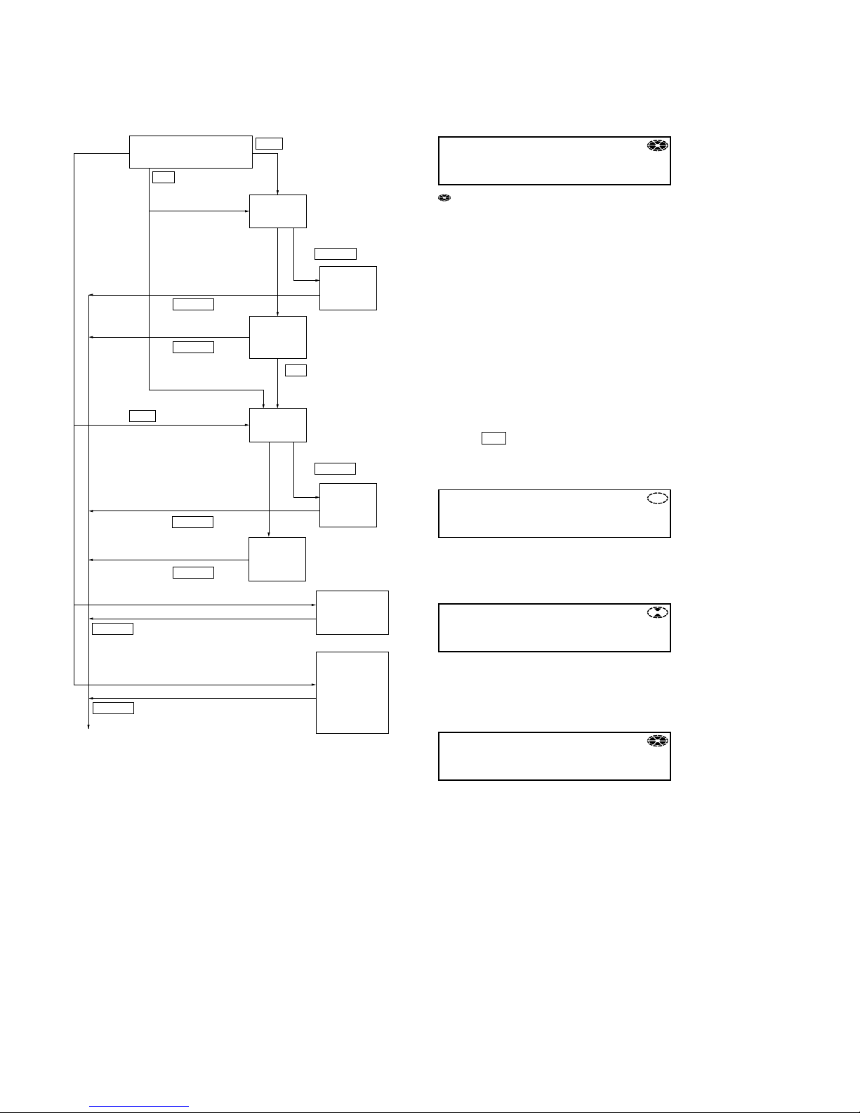
OVERALL ADJUSTMENT MODE
• Configuration of Overall Adjustment Mode
• Overall Adjustment Mode (Title Display)
Assy**
0 00
: (Disc mark) At end of power supply adjustment: Outside lit
At end of electrical offset adj.: Inside lit
**
: Left side = MO overall adjustment information
F*
: MO overall adjustment completed
1*
: Manual adjustment exists (overall adj. not completed)
0*
: Not adjusted
Rifht side = CD overall adjustment information
*F
: CD overall adjustment completed
*1
: Manual adjustment exists (overall adj. not completed)
*0
: Not adjusted
Set LCD display
Assy11
0 00
Set LCD display
Ofst**
0 35
Set LCD display
OfstOK
0 00
Set LCD display
Page 27
27
MZ-N707
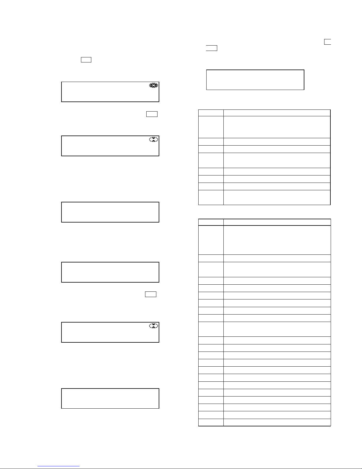
• Adjustment Method of CD and MO Overall Adjustment
Mode
1. Set the test mode (see page 13).
2. Press the . or [VOL --] key to activate the overall adjust-
ment mode.
3. Insert CD disc in the set, and press thethe . key to set the
CD overall adjustment mode. Automatic adjustments are made.
4. In case of CD overall adjustment NG, reset the NV (see page
19), then readjust from the temperature correction (see page
24).
5. If OK through the CD overall adjustments, then perform MO
overall adjustments.
6. Insert MO disc in the set, and press the > key to set the
MO overall adjustment mode. Automatic adjustments are
made.
7. In case of MO overall adjustment NG, reset the NV (see page
19), then readjust from the temperature correction (see page
24).
• CD and MO Overall Adjustment Items
1. CD overall adjustment items
Item No. Description
312
313 CD electrical offset adjustment
314
321 CD tracking error gain adjustment
328 CD TWPP gain adjustment
324
CD
tracking error
offset adjustment
332
336 CD ABCD gain adjustment
344 CD focus gain adjustment
345 CD tracking gain adjustment
521
CD two-axis sensitivity adjustment
522
2. MO overall adjustment items
Item No. Description
112
113
MO electrical offset adjustment
114
118
221 Low reflective CD tracking error gain adjustment
224
Low reflective CD tracking error offset adjustment
232
236 Low reflective CD ABCD gain adjustment
244 Low reflective CD focus gain adjustment
245 Low reflective CD tracking gain adjustment
121 MO tracking error gain adjustment
122 MO TON offset adjustment
134 MO TWPP gain adjustment
131
MO triple speed read TWPP offset adjustment
132
136 MO ABCD gain adjustment
144 MO focus gain adjustment
145 MO tracking gain adjustment
138 MO RF gain adjustment
434 MO write TWPP gain adjustment
431 MO write TWPP offset adjustment
432 MO tracking error offset adjustment
436 MO write ABCD gain adjustment
445 MO write tracking gain adjustment
411 MO normal speed read TWPP offset adjustment
412 MO tracking error offset adjustment
448 20 sec full recording
Assy11
0 00
Set LCD display
CD RUN
X XX
XXX
: Item number for which an adjustment is being executed.
Set LCD display
*** NG
0 00
**
: NG item number.
Set LCD display
CD OK
0 00
Set LCD display
MO RUN
X XX
XXX
: Item number for which an adjustment is being executed.
Set LCD display
*** NG
0 00
**
: NG item number.
Set LCD display
8. If OK through the MO overall adjustments, press the x/
CHG key to return to the test mode and terminate the overall
adjustment mode.
MO OK
0 00
Set LCD display
Page 28
28
MZ-N707
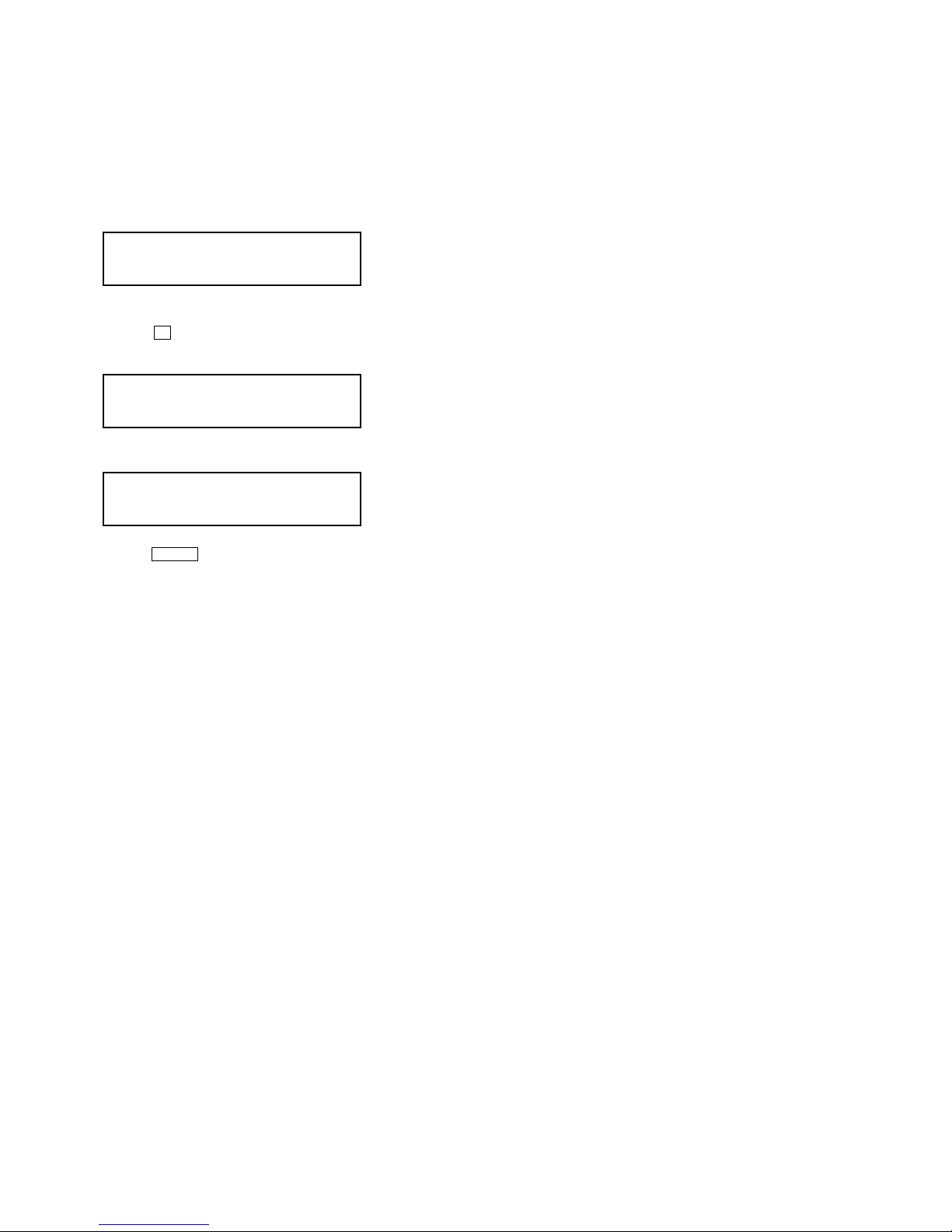
RESUME CLEAR
Perform the Resume clear when all adjustments completed.
• Resume Clear Setting Method
1. Select the manual mode of the test mode, and set item number
043 (see page 14).
2. Press the X key.
3. Press the x/CHG key to return to the test mode (display check
mode).
Res***
0 43
Set LCD display
ResClr
0 43
r
Resume clear complete
###S00
0 43
###
: Address
Set LCD display
Page 29
29
MZ-N707
REWRITING THE PATCH DATA AT REPLACEMENT OF MAIN BOARD OR NONVOLATILE MEMORY
(IC804)
This set requires the patch data in the nonvolatile memory (IC804) to be rewritten using the application, when the MAIN board or
nonvolatile memory (IC804) was replaced.
Caution: The application that meets the microcomputer version in this set must be used when rewriting the patch data. Rewriting the
patch data using the application not suitable for the microcomputer version could cause the set to malfunction.
For a checking method of the microcomputer version, see “SECTION 4 TEST MODE” (page 13).
• Preparation
1. USB cable (attached to the set)
2. Personal computer in which the Net MD Driver has been installed. (For further information, see “System requirements” (page 4) in
“SECTION 1 SERVICING NOTES”)
3. Application “PatchWriter” for patch data rewriting
• How to Get the Application “PatchWriter” for Patch Data Rewriting
Contact our service technical support division to get the application.
• Pre-check
1. Check the microcomputer version in this set. (For a checking method of the microcomputer version, see “SECTION 4 TEST MODE”
(page 13).)
2. Check that the Net MD Driver has been installed in the personal computer.
3. Make sure that the set is in the Normal mode.
Note: Do not rewrite the patch data in the Test mode.
• Rewriting the Patch Data
1. Connect the set to the personal computer with the USB cable.
2. Start the application “PatchWriter”.
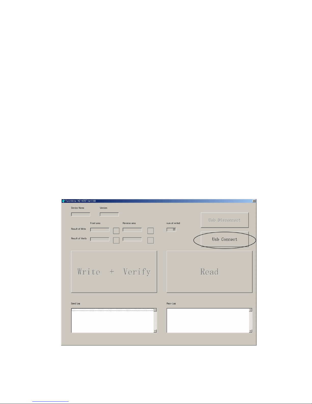
3. Make sure that the following window opens.
4. Click the [Usb Connect] button.
Page 30
30
MZ-N707
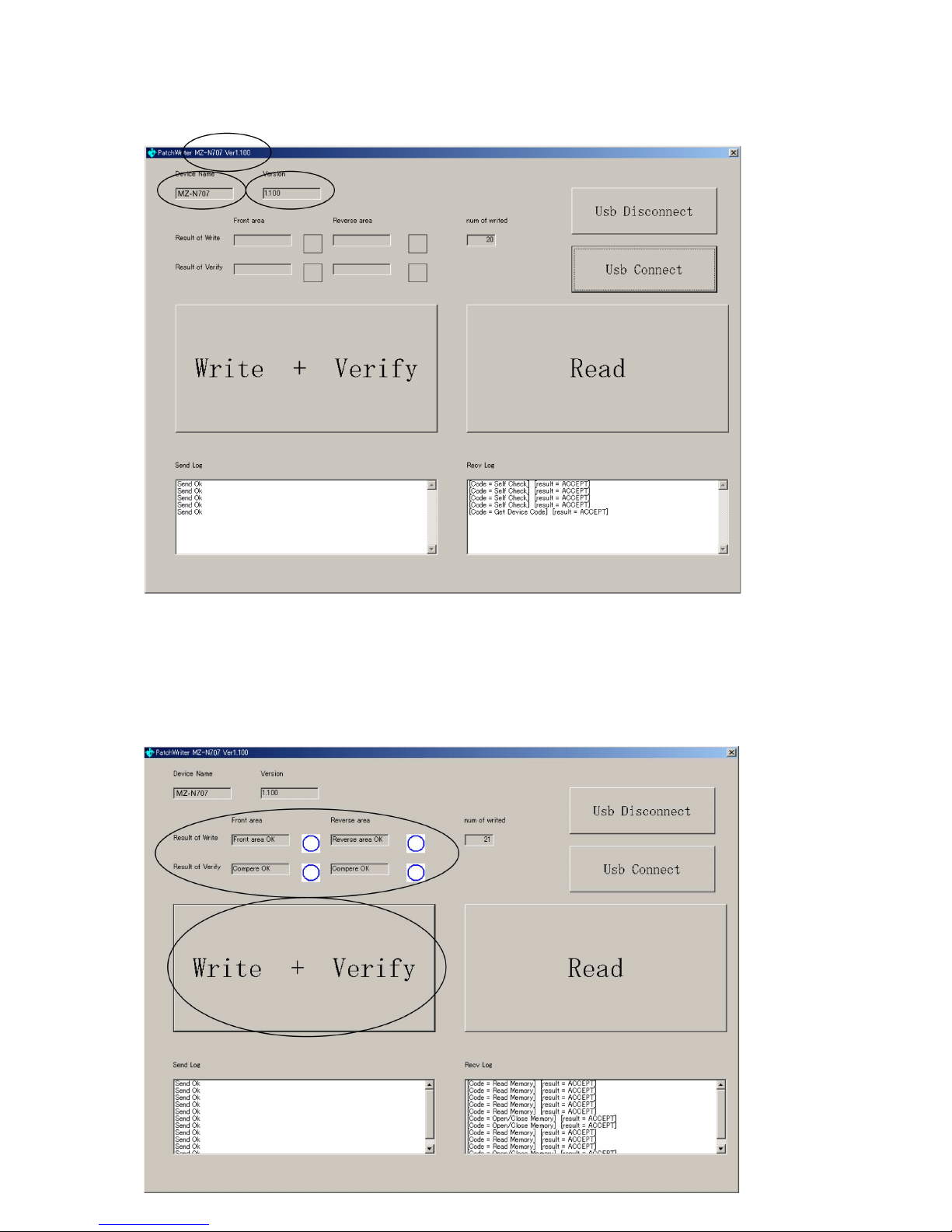
5. Confirm that the model and version indicated on the title bar coincide with the codes displayed in the Device Name block and the
Version block in the window.
6. Click the [Write + Verify] button.
The patch data writing and the verify processing will be executed automatically in the following order:
1) Writing to patch area (front area)
2) Writing to patch area (reverse area)
3) Verifying patch area (front area)
4) Verifying patch area (reverse area)
7. The operation will terminate with the a mark given to all areas.
If the
× mark is given to any area, the nonvolatile memory will be faulty.
Page 31
MZ-N707
3131
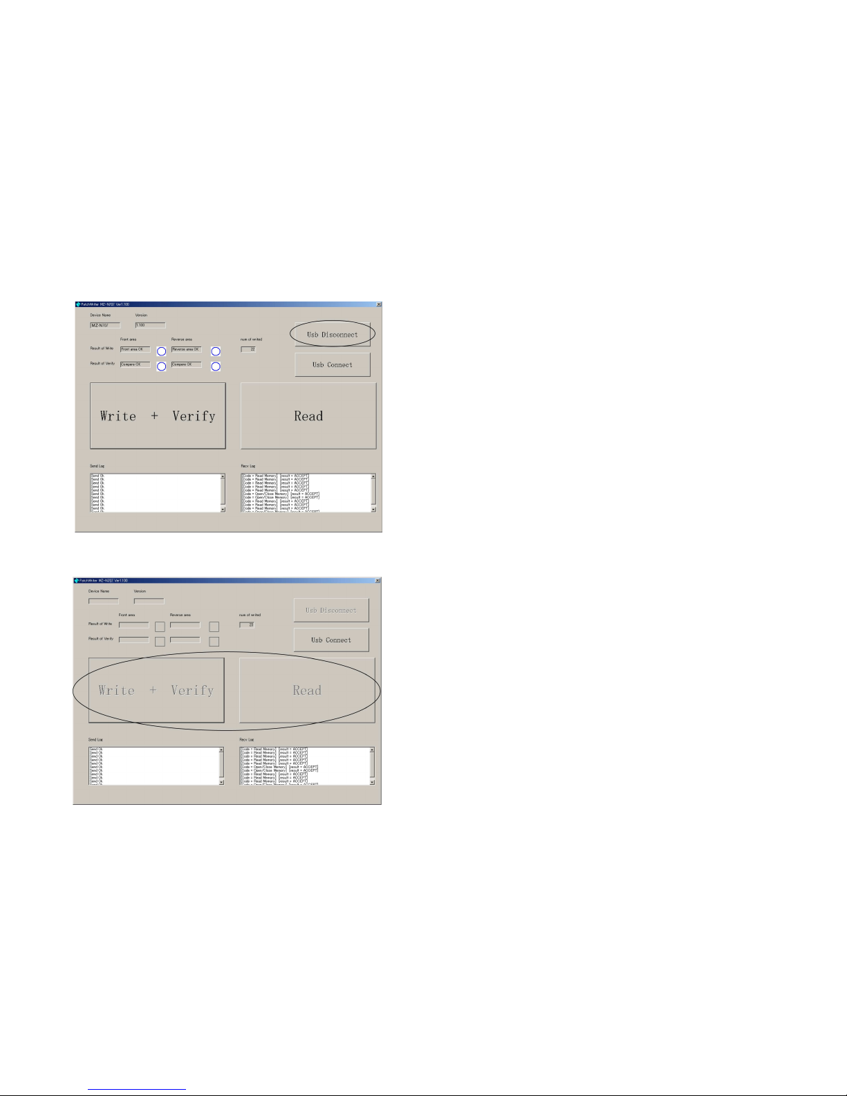
8. Click the [Usb Disconnect] button.
9. Confirm that the window becomes as shown below where the [Write + Verify] button and [Read] button are inactive.
10. Disconnect the USB cable from the personal computer and the set.
Page 32
MZ-N707
3232
33
29
28
41
42
1
44
21
31
25
43
24
23
4
8
9
10
11
12
14
5
6
13
7
18
19
JX JY JX
IX IY
IY
IX
JX
JY
A
B
C
D
MON
IX
ABCD
OPTICAL PICK-UP BLOCK
(LCX-5R)
HR601
OVER
WRITE
HEAD
S0
S1
D
D-C
PD-NI
PD-O
C
B
A
VREF
A-C
JY
JX
IX
IY
RF AMP,
FOCUS/
TRACKING
ERROR
AMP
TPP/WPP
APC
S-MONITER
RF OUT
PEAK
BOTM
ABCD
FE
ADIP IN
TE
ADFG
PD-I
VC
SBUS
SCK
S-MON
XRST
PEAK
/BOTM
RF AMP, FOCUS/TRACKING ERROR AMP
IC501
M603
OVER WRITE
HEAD
UP/DOWN
+
–
+
–
+
–
+
–
+
–
+
–
+
–
+
–
+
–
AUTOMATIC
POWER
CONTROL
Q501
20
LD
SERIAL
INTERFACE
TRK+
FCS+
FCS–
FCS+
TRK–
TRK+
TRK–
163
169
170
171
172
181
202
174
108
75
180
28
80
81
27
26
206
35
33
41
38
37
42
25
30
31
1 2 3 5 6
142 141 140 145 143
4
7
CHARGE
PUMP 2
27
28
CHARGE
PUMP 1
225
226
216
217
218
212
76
222
220
221
219
84
210
209
207
208
16
15
27
28
11
13
32
30
214
215
26
41
44
42
43
1
2
6
4
52 53 54
48 74
35
37
24
39
25
23
45
46
56
55
8
18
19
20
17
230
190
195
155
LD-A
(TRACKING)
(FOCUS)
2-AXIS
DEVICE
OVER WRITE
HEAD DRIVE
Q604, 605
MM
EFM
PRE DRIVER
H-BRIDGE
PRE DRIVER
SYSTEM CONTROL (1/2)
HB
HA
OUTA
OUTB
VREF
C1H
C1L
C2H
C2L
VRECIN2
CLK
EFM
VRECIN1
VRECO
B+
SW
RECONOERI
FI
MODE3
MODE2
MODE1
HD CON2
HD CON1
EFMO
OVER WRITE HEAD DRIVE
IC601 (1/2)
RFI
PEAK
BOTM
ABCD
FE
TE
ADFG
VC
VREF MON
XRF RST
SE
SSB CLK
PD S0
PD S1
SSB DATA
APCREF
SYSTEM CONTROLLER,
DIGITAL SIGNAL PROCESSOR,
16M BIT D-RAM
IC801 (1/3)
• SIGNAL PATH
: PLAYBACK
: REC (ANALOG IN)
: REC (DIGITAL IN)
: USB CHECK OUT
B
C
D
DIN1
ADDT
AOUTL
156AOUTR
134UDP
ADDT
AOUTL,
AOUTR
AOUTL
CLK
SLCU
SLCV
SPCU
SPCV
SPCW
SLD MON U
SLD MON V
CLV MON U
CLV MON V
CLV MON W
SPRD
SPDL MON
SLDW
SFDR
SLDV
SLDR
SLD MON
FRDR
FFDR
TRDR
TFDR
SPDV
SPDW
XRST MTR DRV
RI1
FI1
RI2
FI2
WI2
PWM2
VI2
UI2
VI1
WI1
CPWO1
CPVO1
CPUO1
CLV MON W
CLV MON V
CLV MON U
OE
UI1
PWM1
RO1
FO1
RO2
FO2
FCS–
FCS+
TRK–
TRK+
COM2
VO1
WO1
UO2
VO2
CPVI2
WO2
CPUI2
CPWI2
CPUO2
CPVO2
UO1
CPUI1
CPVI1
CPWI1
COM1
TRACKING
COIL DRIVE
FOCUS
COIL DRIVE
SPINDLE
VOLTAGE MONITOR
SLED
MOTOR
DRIVE
SPINDLE
MOTOR
DRIVE
FOCUS/TRACKING
COIL DRIVE,
SPINDLE/SLED
MOTOR DRIVE
IC551
BIAS
M601
(SPINDLE)
U
WV
M602
(SLED)
U
WV
47
CPWO2
SLD MON U
SLD MON V
SLD MON W
SLED VOLTAGE
MONITER
AOUTR
227SLCW
SLD MON W
213 SPFD
234 MNT3
OFTRK
135UPUEN
133UDM
32DATA+
DATA–
CN701 (1/2)
(USB CONNECTOR)
138UOSCO
137UOSCI
X802
48MHz
A
DIN1
FCS–
(Page 34)
(Page 33)
(Page 33)
(Page 33)
SECTION 6
DIAGRAMS
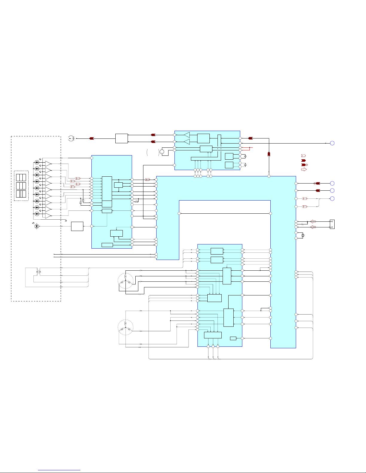
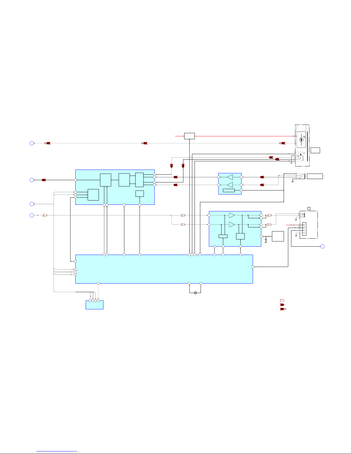
6-1. BLOCK DIAGRAM – SERVO/USB Section –
Page 33
MZ-N707
3333
VC B+
F801
F
RMC KEY
RVDD
DTCK
KEY-R
RGND
(LINE IN JACK)
OPTICAL
RECEIVER
J302
i
J301
LINE IN
(OPTICAL)
J303
MIC
(PLUG IN POWER)
• SIGNAL PATH
: PLAYBACK
: REC (ANALOG IN)
: REC (DIGITAL IN)
3
1214
9
1
2
24
4
23
22
21
15 17
49 69 93
XHP
STBY
3758 36 38198
151
197
45
46
47
171234
B+ SWITCH
Q302
VIF B+
REGULATOR
MUTING
MIC AMP
IC303
IN1
IN2
STBY
OUT2
OUT1
HP/LINE
SWITCH
HEADPHONE AMP
IC302
OUT L
OUT R
OUTB BEEP
OUTA BEEP
IN L
IN R
HP/L
MUTE
BEEP
BEEP
MUTE
XJAC DET
XOPT CTL
FS256
XBCK
OSCO
OSCI
XCS NV1
SDI0
SCK0
SDO0
OPT DET
XMIC DET
RMC DTCK
SYSTEM CONTROLLER,
DIGITAL SIGNAL PROCESSOR,
16M BIT D-RAM
IC801 (2/3)
150
X801
45.1584MHz
SI0
SO0
SCK0
SDI0
SDO0
SCK0
SCK0
SDO0
AOUTL,
AOUTR
ADDT
DIN1
SDO0, SCK0
XCS
SK
DI
DO
B
A
C
E
EEPROM
IC804
2
4
1
3
10
15
14
13
9
GAIN
AMP
CLOCK
DIVIDER
AUDIO
I/F
CONTROL
CONTROL
REGISTER
I/F
A/D
CONVERTER
&
HPF
RIN1
RIN2
LIN1
LIN2
A/D CONVERTER
IC301
SDTO
CCLK
CSN
CDTI
12
LRCK
BCLK
16
PDN11MCLK
196
LRCK
148
XPD ADC
147 XCS ADC
AOUTL
AOUTR
18
120
13
REFERENCE
VOLTAGE
SWITCHING
Q301
VREF IN
+
(Page 32)
(Page 32)
(Page 34)
(Page 32)
(Page 34)
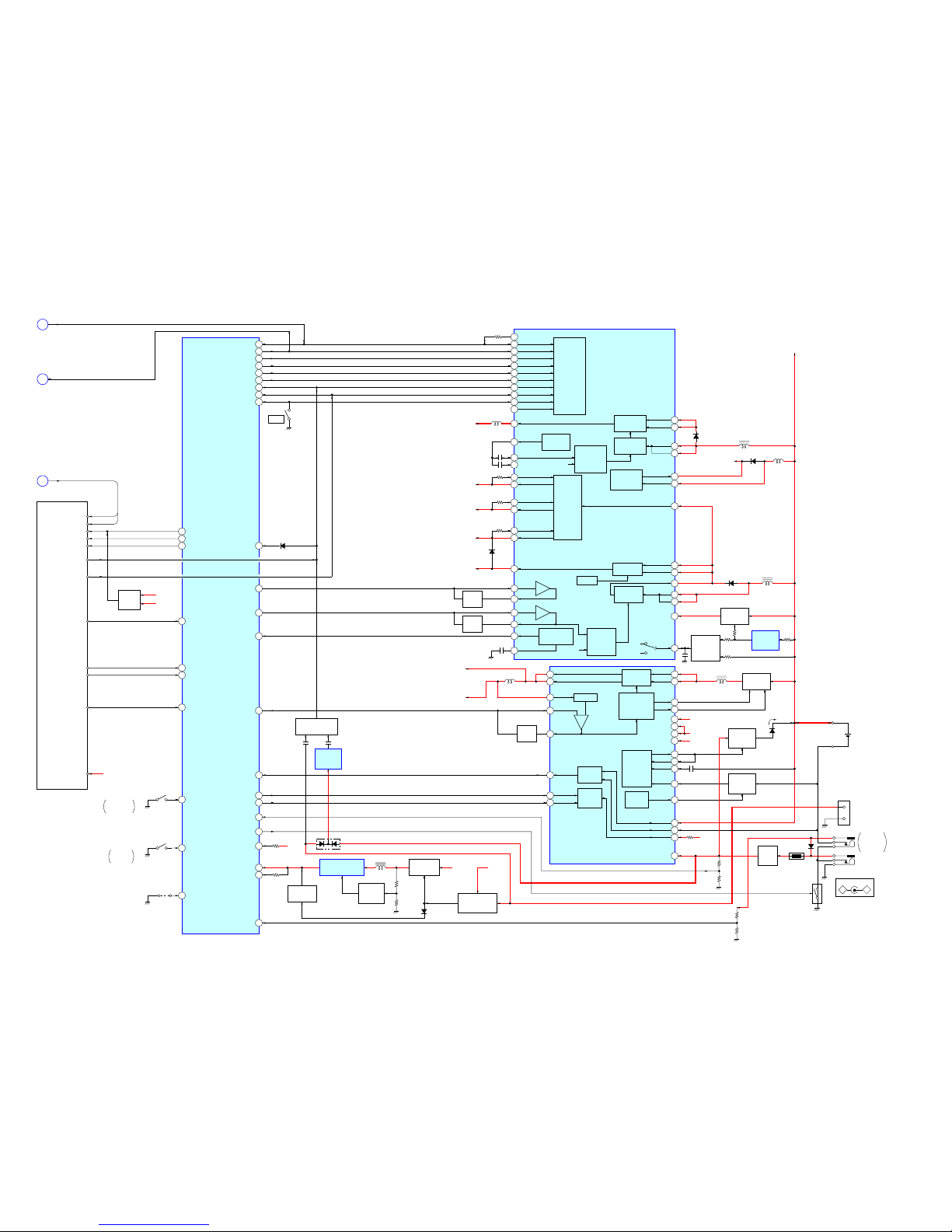
6-2. BLOCK DIAGRAM – AUDIO Section –
Page 34
MZ-N707
3434
7
4
56
52
54
55
1
2
3
5
116
211
64
89
88
85
113
114
115
10
49
24
25
39
44
38
42
40
41
35
22
23
26
46
47
50
28
32
34
11
14
10
15
22
16
19
20
51
54
55
21
8
9
26
49
47
46
45
43
44
56
50
48
33
36
45
18
19
16
12
11
9
27
53
+–
30
31
104
29
107
90
91
112
66
186
82
109
110
39
67
68
102
83
146
77
VB
HEADPHONE AMP (IC302),
MOTOR/COIL DRIVER (IC551)
B+
POWER CONTROL
IC901
SWITCHING
REGURATOR
SYSTEM
CONTROL
BANDGAP
REFERENCE
SERIES
PASS
REGULATOR
REGURATOR
STEP-UP
DC/DC
CONVERTER
STEP-UP
PRE DRIVER
&
PWM
D902
D903
L902
L905
VG
MOTOR/COIL
DRIVER (IC551)
B+
VL
VL
VG
LG
VC2
VC
VC
VOUT
L1
L1
VB
L2
L2
RF2
VRMC
XWK3
CLK
CLK SEL
FFCLR
SLEEP
VLON
XWK1
XWK2
XWK4
VAIFON
VLO
VREF
DTC2
DTC1
VDFB
VIFFB
VIF
VAFB
VA
VCO
INM2
INM1
RF2
RF1
XRST
CRST
DTC1
VD
D904
L904
SYSTEM CONTROLLER,
DIGITAL SIGNAL
PROCESSOR,
16M BIT D-RAM
IC801 (3/3)
RMC KEY
CLK
SDO0, SCK0
VL
RF AMP (501)
LASER APC CIRCUIT
B+
VD
SYSTEM CONTROLLER (IC801)
B+
VIF
A/D CONVERTER (IC301),
SYSTEM CONTROLLER (IC801),
EEPROM (IC804)
B+
VA
A/D CONVERTER (IC301),
SYSTEM CONTROLLER (IC801)
B+
VC
MIC AMP (IC303),
RF AMP (IC501),
MOTOR/COIL DRIVER (IC551),
REMOTE CONTROL CIRCUIT
B+
RMC KEY
FS4
CLK SEL
FFCLR
SLEEP
VLON
WK DET
REC KEY
HALF LOCK SW
OPEN
S805
VIF B+
VB B+
XCS LCD
LCD STB
LCD RST
F
D
E
SDO0
SCK0
SD0
SCK
RST
STB
CS
REC
PAUSE
SE1 KEY 1
SE1 KEY 2
DVDD
HOLD
XWK1
VIF B+
SWITCH & LCD MUDULE
SL801
(TEST)
S803
PROTECT
DETECT
S806
OPEN/CLOSE
DETECT
OPEN CLOSE SW
PROTECT
XTEST
CHG MON
CHG GAIN
CHG
HIDC MON
GND SW
VB MON
PAUSE KEY
SET KEY 1
SET KEY 2
XHOLD SW
VB B+
VL PWM
VC PWM
XRST
VREC PWM
RESET
SWITCH
Q801
NOISE
FILTER
NOISE
FILTER
NOISE
FILTER
L602
VRECO
OVER WRITE HEAD DRIVE
(IC601) B+
SWITCH
SWITCHING
REGULATOR
RESET SIGNAL
GENERATOR
SWITCHING
REGULATOR
CHARGE
CONTROL
CHARGE
MONITOR
POWER
CONTROL
IC601 (2/2)
STEP-UP DOWN
PRE DRIVER
&
PWM
STEP-UP
PRE DRIVER
&
PWM
BATTERY
CHARGER
&
REGULATOR
SYSTEM
CONTROL
(2/2)
VRECO1
VRECO2
VREC
INM1
RF1
CHGMON
GAIN
CHG
L1 1
L1 2
DW BT
DW TP
VIO
VC2
VC
RF2
INM2
INP2
RS
CHG SW
VB
BATM
DREG
DCIN
VIF
B+
VC B+
VIF B+
L601
L901
D901
D603
B+ SWITCH
Q603
CHARGE
CONTROL
Q602 (2/2)
CHARGE
CONTROL
Q602 (1/2)
LINE
FILTER
T601
CHARGE
RECHARGEABLE
BATTERY
NC-WMAA
1PC. 1.2V
OR
DRY BATTERY
SIZE "AA"
(IEC DESIGNATION LR6)
1PC. 1.5V
–
+
DC IN 3V
J601
GROUND
LINE
SWITCHING
Q601
TH601
REGULATOR
SWITCH
36
VG
VG B+
(Page 33)
(Page 32)
(Page 33)
131SUSPEND
D804
6
B+ SWITCH
Q903, 904
SWITCHING
Q901, 902
VOLTAGE
DETECTOR
IC902
VB
VC
VSTB
VREC
OVER WRITE HEAD DRIVE
CIRCUIT B+
132USBIFVDD
111VBUS DET
SWITCHING
Q706
DC/DC CONVERTER
D703, IC702, Q704
VOLTAGE
DETECT
Q703
B+ SWITCH
Q701
105STAND DET
VB B+ VA B+
USB
ON/OFF SWITCH
Q705
D701
L701
D604
J602
FOR
CHARGING
STAND
CN701 (2/2)
(USB CONNECTOR)
1
5
VBUS
GND
WAKE UP SWITCH
Q608
VOLTAGE
DETECTER
IC604
D610
6-3. BLOCK DIAGRAM – DISPLAY/KEY CONTROL/POWER SUPPLY Section –
Page 35
MZ-N707
3535
Note on Schematic Diagram:
• All capacitors are in µF unless otherwise noted. pF: µµF
50 WV or less are not indicated except for electrolytics
and tantalums.
• All resistors are in Ω and 1/
4
W or less unless otherwise
specified.
• % : indicates tolerance.
• C : panel designation.
• A : B+ Line.
• Total current is measured with MD installed.
• Power voltage is dc 3 V and fed with regulated dc power
supply from DC IN 3 V jack (J601).
• Voltages and wav eforms are dc with respect to ground in
playback mode.
no mark : PLAYBACK
( ) : REC
〈〈 〉〉 : USB
∗
: Impossible to measure
• Voltages are taken with a VOM (Input impedance 10 MΩ).
Voltage variations may be noted due to normal production tolerances.
• Waveforms are taken with a oscilloscope.
Voltage variations may be noted due to normal production tolerances.
• Circled numbers refer to waveforms.
• Signal path.
E : PLAYBACK
j : REC (ANALOG IN)
l : REC (DIGITAL IN)
F : USB CHECK OUT
• The voltage and waveform of CSP (chip size package)
cannot be measured, because its lead layout is different
form that of conventional IC.
• Abbreviation
FR : French model
6-4. NOTE FOR PRINTED WIRING BOARD AND SCHEMATIC DIAGRAMS
Note on Printed Wiring Board:
• X : parts extracted from the component side.
• Y : parts extracted from the conductor side.
• : Pattern from the side which enables seeing.
(The other layers' patterns are not indicated.)
Caution:
Pattern face side: Parts on the pattern face side seen from
(Conductor Side) the pattern face are indicated.
Parts face side: Parts on the parts face side seen from
(Component Side) the parts face are indicated.
• MAIN board is four-layer printed board.
However, the patterns of layers 2 and 3 have not been
included in this diagrams.
* Replacement of IC801 used in this set requires a spe-
cial tool.
• Lead Layouts
surfac
e
Lead layout of conventional IC CSP (chip size package)
Note: The components identified by mark 0 or dotted line
with mark 0 are critical for safety.
Replace only with part number specified.
* Replacement of IC801 used in this set requires a spe-
cial tool.
Page 36
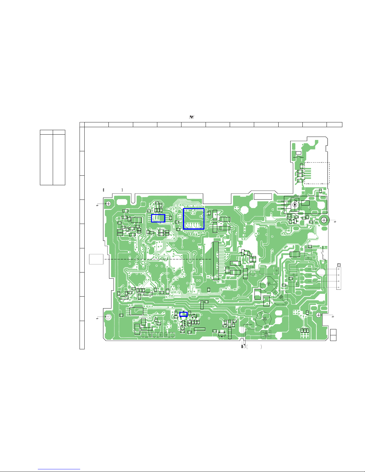
MZ-N707
3636
R317
R320
R302
C803
R853
L902
L901
L601
R936
R914
C913
R603
R602
C605
R915
R947
R917
R105
F801
C330
C111
R319
R316
C211
FB704
FB703
FB702
FB701
J301(1/2)
LINE IN
(OPTICAL)
OPTICAL
RECEIVER
C204
+
C104
+
C316
+
C630
+
L905
L906
C206
R849
R850
R851
L553
L551
L502
L501
L904
L554L552
R521
R522
C518
R519
C904
+
R601
D601
KA
D904
KA
D603
KA
C604
R623
C634
R625
C635
R607
C606
C512
C521
C522
C823
R815
R831
R707
R830
R845
R846
R705
R847
C801
L802
C818
FB802
FB804
C812
R808
R809
R807
R816
FB803
C811
C810
C813
C829
C828
R814
C830
C628
R610
C615
R609
FB805
R863
R855
C825
R803
R802
R832
R839
R840
R844
C834
C608
1
1
14
42
56 43
15 28
29
4
8
5
IC804
IC551
1
4
8
5
D804
KA
D607
KA
D803
AK
C624
+
C612+C611
+
CN501
1
20
OPTICAL
PICK-UP BLOCK
(LCX-5R)
T601
J302 (1/2)
RVDD
DTCK
KEY-R
RGND
ECB
Q302
Q501
E
C
B
S
D
G
Q601
AKA
D610
132
IC604
Q608
B1
B2
E
C1
C2
(11)
11
1-682-873-
S806
(OPEN/CLOSE DETECT)
MAIN BOARD
(COMPONENT SIDE)
C920
CN701
(1/2)
(USB CONNECTOR)
S805
5
1
Q603
OPEN
(CHASSIS)
(CHASSIS)
(CHASSIS)
(CHASSIS)
J602
FOR
CHARGING STAND
A
B
C
D
E
F
G
H
I
1 2 3 4 5 6 7 8 9 10 11
C636
R308
TP (−)
TP (+)
6-5. PRINTED WIRING BOARD – MAIN Board (Component Side) – :Uses unleaded solder.
• Semiconductor
Location
Ref. No. Location
D601 I-7
D603 I-5
D607 I-3
D610 H-5
D803 G-3
D804 H-2
D904 H-5
IC551 D-5
IC604 H-5
IC804 D-4
Q302 D-9
Q501 F-7
Q601 I-6
Q603 H-3
Q608 I-5
Page 37
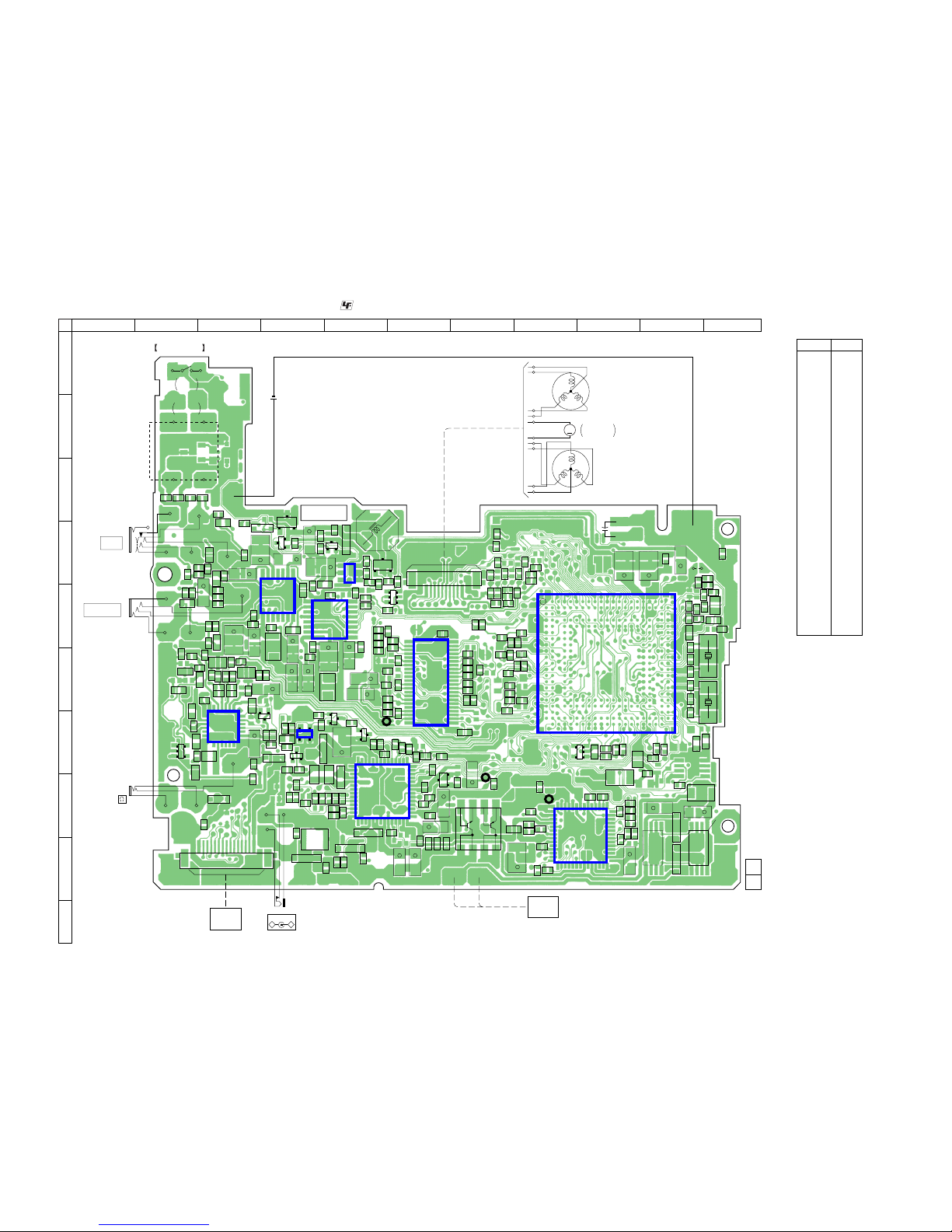
MZ-N707
3737
R704 C340 C321 C325
R111
R703
C110
C210
C117
R112
R318
C327
R218C218
C310
R205
R202
FB306
R211
C116
R212
C326
R102
R118
C118
FB305
C217
C216
C319
C309
C212
C336
R311
FB301
FB303
FB302
C103
C102
R101
R103
R201
R203
C101
C201
C315
C105
C205
FB304
R106
R303
C311
R107 R207
R104 R204
R306
R315
R309
R924
R923
C914
C508
R714
C509
C510
C511
C513
C527
C514
C523
C910
C909
C915
C917
R946
C916
C312
R919
R918
R925
C106
C331
C627 R928
R910
C918
C907
C927
C912
R920
R909
C601
C602
C623
R616
R615
R906
R626
R604
R605
R941
R206
C334
C922
C905
R903
R922
C906
R905
C908
C921
R902
R507
R501
R502
R503
C307
C505
C506
C507
R505
R517
C531
C502
C306
C302
C503C504C530
R916
R921
C501
R948
R908
R907
C924
C928
R927
C515
C516
R305
R304
C308
R709C703
R712
R701
R310
R307
R702
R706R715
R708
C112
R711
R710
C702
R911
R624
C202
C203
C561
C551
R561
R562
C557
C558
C563
R560
R551
R552
C631
R553
C567
C564
C566
C562
C565
C559
R829
R805
R828
C820
C841
C840
R860
R841
R833
C519
C819
C806
R859
C824
C805
R861
R804
R836
C639
R621
R606
R622
R608
C607
C633
R620
C613 C614
R612
C629
C621
R614
R613
C619
C616
C618
R826
C804
R852
R864
R810
C826
C838
R801
C802
R834
R835
R843
FB806
C832 C833 R838 R806 C808 C807
R827
C839
R817
C814
FB801
R821
R823
R824
R858
R825
C822
C816
R822
R857
C817
C323
+
C318
+
C301
+
C324
+
C332
+
C213
+
C704
+
C322
+
C113
+
C317
+
C335
+
C305
+
C529
+
C314
+
C524
+
L303
L301
C320
+
C903
+
C701
+
C901
+
C902
+
C911
+
C919
+
C926
+
C603
+
C622
+
L602
L801
C609
+
C632
+
C809
+
C815
+
C821
+
D701
KA
D902
D903
AK
KA
D101
KA
D201
KA
D602
AK
D604
KA
D901
KA
D703
KA
D606
AK
D608
KA
1
6
18
13
712
24 19
IC302
IC303
IC301
D301
135
4
TH601
ECB
Q301
Q903
BCE
12
43
IC902
ECB
Q902
ECB
Q901
GDS
Q701
Q703
BCE
1
1
135
4
8
16
9
7
148
IC702
Q706
BCE
Q704
BE
C
Q705
E1
B1
C2
C1
B2
E2
IC901
114
15
28
56
43
29 42
IC501
1
22
44
23
Q904
B
C
E
Q602
Q605
114
15
28
56
43
2942
IC601
14
85
Q604
58
41
X802 X801
Q801
B1
B2
E
C1
C2
*
IC801
195
199
178
174
170
166
164
158
156
152
148
143
139
147
130
128
124
120
103
203
180
176
172
168
162
160
154
150
146
142
138
134
137
126
122
175
171
169
167
163
159
155
157
145
151
140
131
133
123
125
135
105
107
197
193
109
111
191
189
141
113
185
187
173
179
177
201
165
161
153
149
144
136
132
129
119
121
127
115
118
183
182
207
181
117
99
101
116
184
186
215
188
96
97
114
112
209
190
211
213
93
91
108
110
192
194
217
204
87
89
104
106
198
196
221
219
83
85
100
102
202
200
226
224
79
75
94
98
206
205
227
225
81
76
92
95
210
208
243
241
77
78
88
90
214
212
237
1
59
74
84
86
218
216
230
228
57
65
80
82
222
220
3
5
4
72
67
63
61
231
223
242
9
11
6
21
25
31
34
10
41
45
49
53
55
71
69
235
239
244
7
8
245
27
33
37
39
43
47
51
54
70
73
232
229
66
68
234
233
240
17
18
19
16
36
28
26
29
32
15
14
44
48
52
58
62
64
238
236
23
12
40
24
35
38
30
13
22
20
42
46
50
56
60
2
MAIN BOARD
(CONDUCTOR SIDE)
J301(2/2)
LINE IN
(OPTICAL)
(LINE IN JACK)
J303
MIC
(PLUG IN POWER)
DC IN 3V
–
+
J601
CN801
115
SWITCH
&
LCD MODULE
HR601
OVER WRITE
HEAD
TP610 TP611
(11)
11
1-682-873-
CN502
110
1
M
10
U
U
N
VW
N
VW
M602
(SLED)
M601
(SPINDLE)
M603
OVER WRITE
HEAD UP/DOWN
L701
SL801
(TEST)
SL506
SL505
RECHARGEABLE BATTERY
NC-WMAA
1PC. 1.2V
OR
DRY BATTERY
SIZE "AA"
(IEC DESIGNATION LR6)
1PC. 1.5V
14
85
S803
PROTECT
DETECT
J302
(2/2)
+
CN701 (2/2)
USB
CONNECTOR
(SHIELD)
A
B
C
D
E
F
G
H
I
J
1 2 3 4 5 6 7 8 9 10 11
C625
AP913
(VLO)
AP912
(VCO)
AP602
(GND)
TP
(VREC)
D101 G-4
D201 H-3
D301 G-2
D602 I-4
D604 I-5
D606 H-10
D608 I-10
D701 D-4
D703 D-5
D901 H-5
D902 G-4
D903 H-5
IC301 E-5
IC302 G-3
IC303 E-4
IC501 F-6
IC601 H-9
IC702 D-5
IC801 F-9
IC901 H-5
IC902 G-4
Q301 G-4
Q602 H-7
Q604 I-10
Q605 I-10
Q701 D-4
Q703 D-4
Q704 D-5
Q705 E-6
Q706 D-5
Q801 G-9
Q901 G-5
Q902 G-5
Q903 G-4
Q904 H-6
6-6. PRINTED WIRING BOARD – MAIN Board (Conductor Side) – :Uses unleaded solder.
• Semiconductor
Location
Ref. No. Location
Page 38
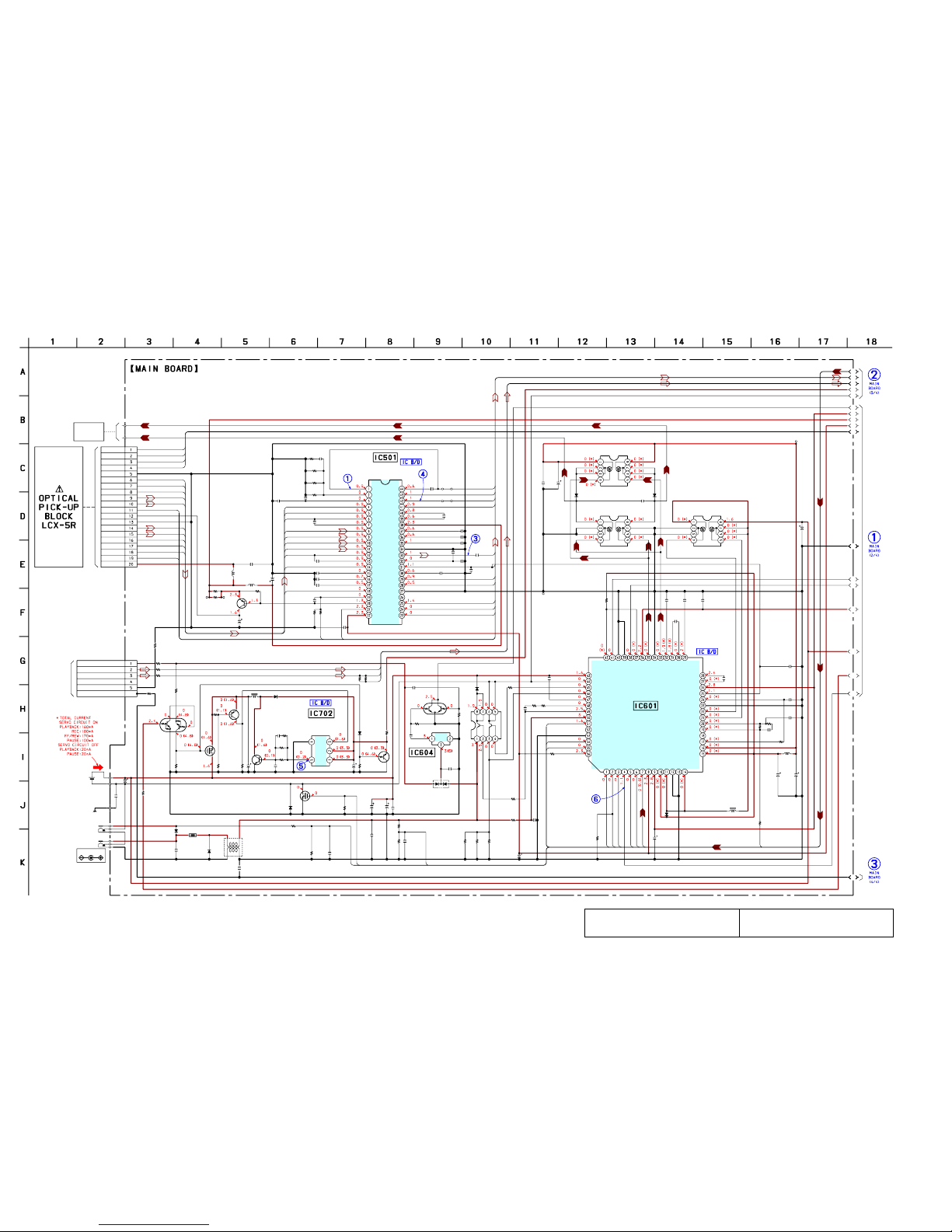
MZ-N707
3838
R507C501
R501
R522
C509
R601
C524
C604
C611
R602
R603 C605
D602
TH601
C505 C515
C508
C510
C511
C513
C514
C516
C519
C606
R608
R621
R607
C633
R620
C619
C618
C613 C616
C614
C615
D608
Q605
D606
C608
Q604
C607
C518
C531
C527
C503
R502
R503
R505 R517
IC604
C634
C628
R623
Q608
R714
R705
R707
R712
R701
R709C703
R703
Q704
Q706
R706 R702
C701
L701
C702
C704
C631
C603
C629
C630
C601
C627
R622
C602
R605R626R604
Q602
J601
C639
C609
D603
C622 C624
L501
R519
C502
C506
C507
C504
C530
C523
D607
C612
L502
R521
R612
R613
C621
C632
R614
D601
R606
CN501
TP611
TP610
SL506
SL505
R609
R610
L602
L601
C529
C635
C636
D610
R625
R624
R711D701
R710
D703
R708
R704
FB702
C623R616
R615
CN701
R715
FB701
FB703
FB704
C625
D604
TPTP
AP602
TP
1k 100p
47k
1
2200p
1M
10
6.3V
0.01
10
6.3V
220k
100k 1000p
MA2YD15
0.01
0.1
0.1
10p
10p
10p
0.022
0.1
4700p
100p
220k
10k
220
0.1
10k
0.1
0.1
0.1 0.1
0.1
100p
MA2YD17
HAT2050T
MA2YD17
0.1
HAT2051T
100p
4.7
0.01
0.047
2200p
220k
470k
10k
0.5%1k0.5%
XC61FS1YXXMR
0.1
0.01
100k
XP1210
0
2.2k
4.7k
4.7k
1k
1001000p
470k
FMMT617
UN9115
100k 470k
22
6.3V
2200p
47
10V
220
4V
100
6.3V
100p
220
6.3V
0.01
0.1
100k
0.1
12.21
ZDT6718
0.1
47
4V
MA2YD15
474V10
6.3V
100k
0.022
0.022
0.022
2200p
2200p
1
MA2YD15
10
6.3V
1
470k
2.2k
0.01
10
6.3V
10k
MA2YD15
470
20P
1
1%
22k
10
6.3V
0.1
0.1
RB715W
100k
10
0MA729
2.2k
MA2YD15
470k
0
0
1000p1k
2.2k
5P
47k
0
0
0
1000p
MA2YD15
(-)(+)
(GND)
(VREC)
A1
A2
A3
A4
A5
A6
A7
A8
A9
A10
A11
A12
B1
B2
B3
B4
B5
C1
MODE1
M
ODE2
MODE3
EFM
ADIP
TRK-
TRK+
FCS-
FCS+
BOTM
PEAK
RFI
ABCD
FE
TE
A1
A2
A3
A4
A5
A6
A7
A8
A9
A10
A2
A3
A1
A4
A5
A6
A7
A8
A9
A10
SDAT
SCLK
XRST
PDS1
PDS0
VMON
SMON
AREF
CHGG
CHGM
VRP
HMON
GSW
HC2
HC1
UDM
UDP
UEN
CHG
SDET
VB
BATM
CHGSW
RS
INP2
INM2
RF2
DCIN
CHGMON
SVREF
GND
GAIN
CHG
DREG
SW
RECON
OE
CLK
RI
FI
EFM
VIO
VC
VRECO1
L1 1
PGND1
L1 2
C1
C1
C2
C2
E2
B2
E1
B1
S
DC IN 3V
TE
REXT
VREF
C
D
D-C
Iy
Ix
Jx
Jy
A
A-C
B
TON-C
CIG
CDN
PD-O
DVDD
-LPF
WPP
PD-NI
PD-I
ADFG
(1/4)
S
GND
EXT
PGND2
D2
S2
G2
D1
S1
G1
D2S2D1
S1
G1 G2
D2S2D1
S1
G1 G2
Q604,605
OVER WRITE
HEAD DRIVE
Q608
WAKE UP
SWITCH
-1-2
I
GO
VOLTAGE
DETECTOR
Q602
CHARGE
CONTROL
SWITCHING
DC/DC
CONVERTER
(CHASSIS)
-1
-2
(USB CONNECTOR)
D703,Q704
10µH
10µH
22µH
10µH
10µH
IC501
SN761057ADBT
RF AMP,
FOCUS/TRACKING ERROR AMP
S-MON
FE
ABCD
OFC-1
OFC-2
AVCC
PS
LP
EQ
AGND
RFOUT
CCSL2
VC
PEAK
BOTM
DGND
OFTRK
SCK
SBUS
ADIP
-IN
075
VREF
XRST
Q501
2SA1577
AUTOMATIC
CONTROL
POWER
Q705
UMD12N
USB ON/OFF
SWITCH
Q601
SI2302DS
SWITCHING
GROUND LINE
VOUT
VDD
CE
Q701
KP151A12A2MR
B+ SWITCH
Q703
2SB1462J
VOLTAGE
DETECT
IC702
XC6367A361MR
DC/DC
CONVERTER
T601
LINE FILTER
RECHARGEABLE BATTERYRECHARGEABLE BATTERY
DRY BATTERY
SIZE"AA"
1PC. 1.5V
NC-WMAA
1PC. 1.2V
OR
(IEC DESIGNATION LR6)
J602
(FOR CHARGING STAND)
GND
VBUS
DATA-
DATA+
ID
(SHIELD)
TRK-
TRK+
FCS-
FCS+
AGND
VREF
C
D
S0
LD-A
LD-K
A
B
MON
SI
AVCC
Iy
Ix
Jx
Jy
HR601
OVER WRITE
HEAD
Q603
TS8K1
B+ SWITCH
VRECIN1
OUTA
PGND2
PGND2
OUTB
VRECIN2
VG
HB
PGND3
HA
VG3
C2L
VG2
C2H
C1H
C1L
VC2
VREF
CVREF
GND
DW BT
DW TP
RF1
INM1
INP1
DTC
VREC
VRECO2
IC601
XPC18A22AFCR2
POWER CONTROL,
OVER WRITE HEAD DRIVE
6-7. SCHEMATIC DIAGRAM – MAIN Board (1/4) –• See page 42 for Waveforms. • See page 43 for IC Block Diagrams.
The components identified by mark 0 or dotted
line with mark 0 are critical for safety.
Replace only with part number specified.
Les composants identifiés par une marque 0 sont
critiques pour la sécurité. Ne les remplacer que
par une pièce portant le numéro spécifié.
(Page 40)
(Page 39)
(Page 41)
Page 39
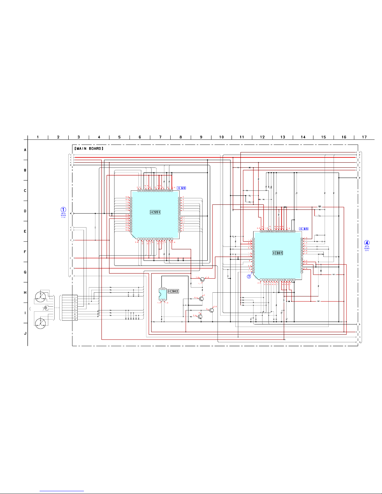
MZ-N707
3939
R905
C922
C906
C921
C908
C905R903
R902
R941
D903
L904
C903
L902
R909 R910
D901
C914
R920
R911
C512
C919
C920
D902
L905
C561
R922
C521
C522
C551
C918
R914
R906
R917
R936
C926
C910
C907
R924
R923
R925
Q903
Q904
R921
R916
R907
R908
C928
C913C912
C909
C562
C565
C563
C566
C567
C564
R551
R552
R553
Q902
Q901
R560
R561
R562
R927
C924
D904
R915
C911
R947
R918
C917
C915
L906
CN502
L901
IC901
R948
C902C901
R946
L551
L552
L553L554
R928
R919
C916
C927
C557 C558 C559
C904
AP913
AP912
2.2k
1000p
0.01
0.1
0.1
0.12.2k
470k
22k
MA729
100
6.3V
10k 10k
MA2YD15
0.1
10k
0.5%
470
0.1
10 6.3V
10 6.3V
MA2YD15
0.1
22k
0.1
0.1
0.1
2.2
100
0
4.7k
0.5%
22k
0.5%
10
6.3V
1000p
2.2
220k
220k
220k
2SD2216J-R
2SA1745
470k
220k
1M
100k
0.1
4700p1000p
1000p
0.022
0.01
0.022
0.01
0.01
0.022
10k
10k
10k
2SD2216J-R
2SD2216J-R
2.2k
2.2k
2.2k
1M
1000p
MA111-TX
2.2k
0.5%
10
6.3V
1k
0.5%
10k
0.5%
0.1
0.1
10P
XPC18A32FCR2
100k
0.5%
10
6.3V
10
6.3V
10k
0.5%
0
0
00
100k
47k
0.5%
1
0.1
0.047 0.047 0.047
22
6.3V
(VLO)
(VCO)
A1
A2
A3
A4
A5
A6
A7
A8
A9
A10
A11
A12
D1
D2
D3
D4
D5
D6
D7
D8
D9
D10
D11
V
L
O
N
FCS- FCS+
T
R
K
-
T
R
K
+
C1
C2
C3
C
1
C
2
C
3
C
4
C
5
C
6
C4
C5
C6
D1
D2
D3
D5
D6
D7
D4
D8
XRST
SCW
SCV
SCU
SP
SMU
SMV
SMW
XMD
CMW
CMV
CMU
CP
CCU
C
C
V
C
C
W
R
E
C
K
H
A
L
F
W
D
E
T
CSEL
FF
SL
ZZ1ZZ2ZZ3
VCP VLP
P
GN
D2
NC
VD
VC2
XRST
CRST
RSTREF
VREF
VB
GND
CLKSEL
VAIFON
FFCLR
SLEEP
CLK
V
LON
XW
K
1
XW
K
2
X
W
K
4
XW
K
3
V
STB
VR
M
C
G
N
D
VL
V
LO
VL
L
2
PG
N
D2
UI2
PWM2
CPUO2
CPVO2
CPWO2
OE
GND1
VC
VG
CPWO1
CPVO1
CPUO1
PWM1
UI1
V
I1
W
I1
PGN
D
W
1
W
O
1
VM
VW
1
VO
1
PG
N
D
UV
1
U
O1
VM
U
1
VM
R
1
R
O
1
PG
N
D1
FO
1
VM
F1
(2/4)
GN
D
N
C
VD
D
O
UT
V
U
N
W
(SLED)
(SPINDLE)
M602
V
U
N
W
M601
1
10
POWER CONTROL
B+ SWITCH
Q903,904
Q901,902
SWITCHING
10µH
100µH
100µH
10µH
22µH
IC551
SC111258FCR2
FOCUS/TRACKING COIL DRIVE,
SPINDLE/SLED MOTOR DRIVE
W
M
F2
FO
2
PG
N
D
2
R
O
2
VM
R
2
V
M
U
2
U
O2
P
G
N
D
UV
2
V
O
2
V
M
V
W
2
W
O
2
PG
N
D
W
2
W
I2
V
I2
FI1
RI1
COM1
CPUI1
CPVI1
CPWI1
GND2
NC
CPWI2
CPVI2
CPUI2
COM2
RI2
FI2
IC902
XC61CN0802NR
VOLTAGE
DETECTOR
NC
L2
PGND2
LG
VG
INM2
RF2
DTC2
DTC1
INM1
RF1
L1
VGFB
VDRF
P
GN
D1
N
C
L1
V
COU
T
VC
V
CO
VC
G
ND
V
IFFB
VD
FB
VA
FB
VA
V
IF
PG
N
D1
D1
D2
D3
TF1
TR1
FR1
FF1
D5
D6
D7
D4
D8
SLEDN
SLEDU
SLEDV
SLEDW
HD DRV-
HD DRV+
CLVW
CLVV
CLVU
CLVN
M603
OVER WRITE
HEAD UP/DOWN
6-8. SCHEMATIC DIAGRAM – MAIN Board (2/4) –• See page 42 for Waveform. • See page 43 for IC Block Diagrams.
(Page 38)
(Page 40)
Page 40
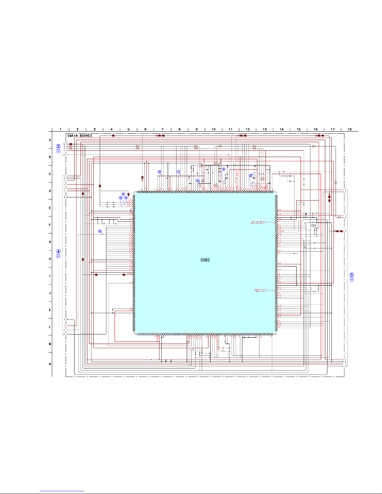
MZ-N707
4040
L802
R
8
4
4
R
8
4
6
R
8
45
R
8
0
6
C841 C820
R829
C819C840
R828
C801
C834 D804
R839
R815
R816
R831
FB802
FB803
FB804
FB806
C833
C
8
32
X
8
0
2
S
L
8
0
1
C806
C821
C822
C808
C809
C
8
2
8
C
8
2
9
C
8
1
0
C
8
1
1
C
8
1
2
C
8
1
3
R
8
0
8
R
8
0
9
R
8
1
4
R823
C
8
1
6
R
8
2
2
R825
R858
R857
R824
C817
C
8
1
5
C814
R
8
1
7
R859
C824
R833
R805
R860
R804
C805
R861
C839
R807
C838
D
80
3
R803
R840C825
C802
C804
R801
R847
R841
R836
C803
R821
FB801
R832
L801
S805
C818
C
8
0
7
X
8
0
1
R
8
43
R
8
3
8
R
8
2
7
R834
R852
R835
R802
0
22
22
4
7
0
4700p 0.01
4.7k
0.5% 0.0220.01
2.2k
0.5%
0.1
0.01 MA729
1M
0
0
0
0
0
0
0
10p
1
0
p
4
8
M
H
z
0.047
47
6.3V 0.1
10p
22
6.3V
1
1
1
1
0
.0
1
0
.4
7
1
0
k
1
0
0
k
1
0
220
0
.1
1
k
2.2M
1M
1k
2.2k
1
4
7
6
.3
V
470p
1
0
0
k
1k
0.047
2.2k
2.2k
1k
2.2k
0.047
1k
1000p
10
4.7
M
A
80
6
8
-
T
X
47k
0.5%
100100p
0.01
0.1
220k
0
0
0
0.01
220k
0
470k
0
0.1
1
0
p
4
5
.1
5
8
4
M
H
z
0
4
7
0
0
100k
0.5%
68k
0.5%
470k
0.5%
4.7k
0.5%
B1
B2
B3
B4
B5
D1
D2
D3
D4
D5
D6
D7
D8
D9
D10
D11
E1
E2
E3
E4
E5
E8
E9
E10
E11
U
D
M
U
D
P
U
E
N
V
R
P
R
F
I
VMON
PDS1
PDS0
XRST
S
D
A
T
S
C
L
K
V
L
P
V
C
P
A
R
E
F
A
D
IP
T
E
S
M
O
N
V
M
O
N
F
E
A
B
C
D
B
O
T
M
P
E
A
K
E
F
M
H
C
2
H
C
1
M
O
D
E
1
M
O
D
E
2
M
O
D
E
3
HMON
CHGM
SDET
CHG
CHGG
GSW
HALF
RECK
WDET
XRST
FF
SL
VLON
C
S
E
L
Z
Z
1
XMD
CCU
SCU
SMW
SMV
SMU
SCW
SCV
SP
SCU
CMW
CMV
CMU
CCW
CCV
CP
CCU
FR1
FF1
TF1
TR1
SK2
SK1
LR
PAUSE
XHOLD
NV
LS
XL
S
D
I0
S
D
O
0
S
C
K
0
B
1
B
2
XS
MUTE
X
O
C
T
L
B
E
E
P
X
M
D
E
T
X
J
D
E
T
O
P
D
E
T
DTCK
ADDT
LRCK
FS256
DIN1 XPD XCS
XBCK
RECP
TX
MNT3
MNT2
MNT1
MNT0
EFMO
SLCW
SLCV
SLCU
SLDW
SLDV
SFDR
SRDR
FRDR
FFDR
TFDR
TRDR
APCREF
ADFG
FS256
XBCK
ADDT
DADT
NC
NC
A
O
U
T
S
E
L
D
R
A
M
V
S
S
1
D
R
A
M
V
D
D
1
NCNCNC
NCNCNC
NC
D
R
A
M
V
D
D
0
D
R
A
M
V
S
S
0
NCNCNCNCNC
NC
N
C
NC
NC
N
C
D
V
S
S
0
D
V
D
D
0
O
F
T
R
K
S
S
B
D
A
T
A
S
S
B
C
L
K
V
R
E
C
P
W
M
V
L
P
W
M
V
C
P
W
M
N
C
IF
V
D
D
0
IF
V
S
S
0
O
P
T
D
E
T
X
J
A
C
K
D
E
T
X
M
IC
D
E
T
O
P
E
N
C
L
O
S
E
S
W
S
E
T
C
O
D
E
0
S
E
T
C
O
D
E
1
S
E
T
C
O
D
E
2
S
E
T
C
O
D
E
3
X
P
A
T
C
H
S
I0
S
O
0
S
C
K
0
X
G
U
M
O
N
B
E
E
P
T
E
S
T
1
T
E
S
T
0
K
D
I
K
D
O
T
R
S
T
X
O
P
T
C
T
L
V
G
C
T
L
K
R
B
K
C
L
K
K
C
S
T
S
B
S
S
B
C
T
L
R
E
C
O
P
R
L
E
D
G
N
D
S
W
2
CLK SEL
IFVSS3
IFVDD3
NC
DVDD3
DVSS3
NC
NC
FS4
SPRD
SPFD
SPDV
SPDW
SPCU
SPCW
SPCV
DVSS4
DVDD4
IFVDD4
IFVSS4
SENS
LRCKI/XELT
XBCKI/ECK
DATAI/EDT
XERQ
A11
XOE
XWE
TSTDR3
EVA
FLASHVDD
FLASHVSS
ITO
(3/4)
N
C
(V
D
P
W
M
)
NC
NC
NC
NC
NC
NC
NC
NC
(
T
E
S
T
)
OPEN
LRCK
10µH
M
O
D
E
1
M
O
D
E
2
M
O
D
E
3
H
D
C
O
N
1
H
D
C
O
N
2
X
T
E
S
T
X
C
S
A
D
C
X
P
D
A
D
C
P
B
V
D
D
V
D
IO
S
C
O
S
C
I
O
S
C
O
V
S
IO
S
C
D
A
V
D
D
V
R
E
F
L
V
R
E
F
R
D
A
V
S
S
A
S
Y
O
A
S
Y
I
A
V
D
1
B
IA
S
R
F
I
A
V
S
1
P
C
O
F
IL
I
F
IL
O
C
L
T
V
P
E
A
K
B
O
T
M
A
B
C
D
F
E
A
U
X
1
V
C
A
D
IO
A
D
R
T
A
V
D
2
A
V
S
2
A
D
R
B
S
E
T
E
D
C
H
G
A
P
C
C
K
R
F
D
T
R
F
X
L
R
F
D
V
S
S
2
D
V
D
D
2
X
T
S
L
D
IN
1
N
C
NC
M
IT
Y
S
U
S
P
E
N
D
U
S
B
IF
V
D
D
U
D
M
U
D
P
U
P
U
E
N
U
S
B
O
S
C
V
D
D
U
O
S
C
I
U
O
S
C
O
U
S
B
O
S
C
V
S
S
A
O
U
T
L
A
O
U
T
R
LCD STB
PROTECT
SLEEP
FFCLR
CHG GAIN
XRST
VB MON
CHG MON
VREF MON
SET KEY 1
SET KEY 2
HIDC MON
WK DET
REC KEY
HALF LOCK SW
RMC KEY
AVDD
AVSS
JOG A
JOG B
XHP STBY
PD S0
PD S1
PAUSE KEY
SLD MON
VLON
DVSS1
DVDD1
CHG CTL
CHGI CTL
IFVSS2
IFVDD2
T MARK SW
NC
NC
VBUS DET
TSMVDD
RMC DTCK
TSLVDD
NC
NC
TAT
TAN
NAR
IDO
SAK
XMUTE
STAND DET
LCD RST
XUDP UP ON
XCS NV2
XCS LCD
SENSE
MIC
GND SW
MUTE
CS RTC
XCS NV1
IFVDD1
IFVSS1
XRST MTR DRV
XRF RST
SPDL MON
XHOLD SW
NC
IC801
CXD2677-202GA
CSP(Chip Size Package)
∗
SYSTEM CONTROLLER,
16M BIT D-RAM
DIGITAL SIGNAL PROCESSOR,
S803
PROTECT
DETECT
S806
OPEN/CLOSE
DETECT
6-9. SCHEMATIC DIAGRAM – MAIN Board (3/4) –• See page 42 for Waveforms.
(Page
38)
(Page
39)
(Page
41)
Page 41
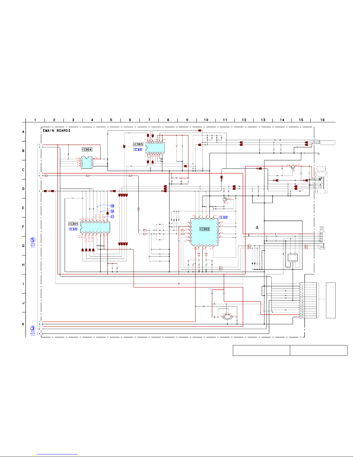
MZ-N707
4141
R118 R218
C203
C202
C103
C102
C826
L301
C302C306
C305
R304
R305
C308
R211 R111
R212
R112
C211 C111
C340 C321
R302 C330
R307
R317
C218 C118
C112
C212
C217
C117
R102 R202
C324
R319
C327
C317 C318
C309
C323
C213
C113
R830
C823
IC804
R849
R850
R851
FB805
R810
R863
R855 R853
R309
C312
C334
C206
C106
C319
FB301
D301
C336
R105 R205
C204
C205
R206
C105
R106
C104
C201
R201
R203
R103
R101
C314
R320
R303
R207
R107
R104
R204
R315
R306
C110
C210
R318C325 C326
R316
C316
C307
C335
C301
R310
R864
C322
C332
C311
R311
C830
C216C116
C101
IC301
J303
CN801
FB303
FB304
FB302
J302
C331
F801
D101
D201
IC303
R826
FB306
FB305
C310 R308
L303
C315
Q301
C320
22k
0.5%
22k
0.5%
2200p
4700p
2200p
4700p
0.22
0.10.1
2.2
6.3V
1k
1k
0.1
22k
0.5%
22k
0.5%
47k
0.5%
47k
0.5%
100p 100p
0.1 0.1
1k 0.1
100
100
2200p 2200p
1
1
0.47
0.47
10k
0.5%
10k
0.5%
10
6.3V
1k
1000p
22
6.3V476.3V
0.047
10
6.3V
47
4V
47
4V
1M
0.1
AK6417AM
0
0
0
0
100k
100k
00
220k
2.2
0.1
1000p
1000p
0.01
NNCD6.8H
220p
4.7k 4.7k
220
2.5V
0.22
10
0.22
10
220
2.5V
22k
47k
47k
22k
10
6.3V
10k
47
10k
10k
10k
22k
1
1
1k1000p 1000p
100k
10
4V
0.1
10
6.3V
47
6.3V
0
100k
47 6.3V
10 6.3V
0.1
1M
0.1
1000p1000p
AK5354VT
15P
0
0
0
1000p
0.25A
125V
02DZ2.4-Z
02DZ2.4-Z
NJM2173AV
0
0
1000p 0
1
SC4738FL
4.7
4V
C1
E1
E2
E3
E4
E5
E8
E9
E10
E11
BEEP
M
U
T
E
SCK0
SDO0
SDI0
DIN1
A
D
D
T
X
B
C
K
F
S
2
5
6
L
R
C
K
S
C
K
0
S
D
O
0
SDO0
X
M
D
E
T
ZZ1
ZZ2
ZZ3
OPDET
XJDET
XOCTL
NV
PAUSE
SK2
SK1
XHOLD
LS
XL
SCK0
LR
X
S
B2
B1
X
P
D
X
C
S
D
T
C
K
∗
∗
∗
∗
XCS
SK
DI
DO
(CHASSIS)
L
IN
1
R
IN
1
L
IN
2
R
IN
2
VC
O
M
A
G
N
D
VA
V
D
PAUSE
XWK1
SET KEY 1
REC
CS
STB
SDO
SCK
DVDD
RST
(4/4)
SET KEY 2
DGND1
HOLD
S GND
DGND2
B
+
OUT L
PW
G
N
D
O
U
T
R
AGC IN
D
ET
VREF INSTB
TCMT
VCC
IN R
IN L
OUTB BEEP
OUTA BEEP
O
U
T1
IN
1
D
C
C
U
T
1
M
IC
V
+
1
R
EG
G
N
D
NOISE
SWITCH
LCD
MODULE
&
-1 -2
4.7k
10k
22k
(FR)
(EXCEPT US,FR)
(US)
∗
R104,204
(US)
∗
C101,201
(EXCEPT US)
MIC AMP
EEPROM
A/D CONVERTER
REFERENCE
SWITCHING
VOLTAGE
10µH
10µH
VCC
XBUSY
RST
GND
V
+
G
V
IN
2
O
U
T2
D
C
C
U
T2
M
IC
V
+2
STBY
MIC
(PLUG IN POWER)
J301
LINE IN
(OPTICAL)
OPTICAL
RECEIVER
LINE IN
JACK
Q302
2SA2018TL
B+ SWITCHB+ SWITCH
RVDD
DTCK
KEY-R
RGND
HP-GND
HP-L
HP-R
IC302
TA2131FL
HEADPHONE AMP
BST
NF2
LPF2
NF1
LPF1
VREF
M
U
T
E
BE
EP
G
N
D
BS
T S
W
Q801
XP1501
RESET SWITCH
P
D
N
C
S
N
C
C
L
K
C
D
TI
LR
C
K
M
C
L
K
BC
LK
S
D
TO
2.2
0.47
6-10. SCHEMATIC DIAGRAM – MAIN Board (4/4) –• See page 42 for Waveforms. • See page 43 for IC Block Diagrams.
The components identified by mark 0 or dotted
line with mark 0 are critical for safety.
Replace only with part number specified.
Les composants identifiés par une marque 0 sont
critiques pour la sécurité. Ne les remplacer que
par une pièce portant le numéro spécifié.
(Page 40)
(Page 38)
Page 42
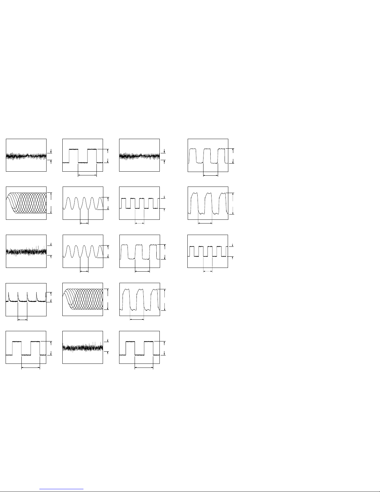
MZ-N707
4242
720 mVp-p
10
µ
s
100 mVp-p
1 Vp-p
• Waveforms
1 IC501 1 (TE)
200 mVp-p
4 IC501 rs (FE)
6 IC601 4 (CLK)
1 Vp-p
5.67 ns
5 IC702 5 (EXT) (USB mode)
7 IC901 th (CLK)
8 IC801 <zc, (UOSCO) (USB mode)
1.9 Vp-p
20.8 ns
1 Vp-p
5.67 ns
9 IC801 <zbz (OSCO)
3 Vp-p
22.1 ns
3 IC501 ed (RF OUT)
200 mVp-p
0 IC801 <znc (RFI)
qa IC801 <zmx (FE)
qs IC801 <z,z (TE)
1 Vp-p
100 mVp-p
qd IC801 <z.n (LRCK) (REC mode)
2 Vp-p
22.7
µ
s
qf IC801 <z.m (XBCK) (REC mode)
qg IC801 <z., (FS256) (REC mode)
2.2 Vp-p
354 ns
2.5 Vp-p
88.6 ns
qh IC801 <xzz (FS4)
1 Vp-p
5.67 ns
ql IC301 qs (LRCK) (REC mode)
2 Vp-p
22.7
µ
s
qk IC301 qa (MCLK) (REC mode)
2.5 Vp-p
88.6 ns
qj IC301 0 (BCLK) (REC mode)
2.2 Vp-p
354 ns
Page 43
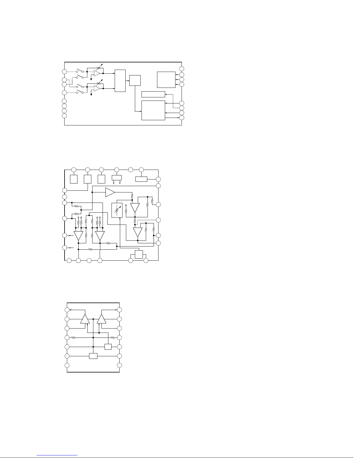
43
MZ-N707
1
2
3
4
5
6
7
AMP1
14
13
12
11
10
9
8
AMP2
REG
GV
OUT1
DC CUT1
IN1
MIC V+1
REG
NOISE
GND
OUT2
DC CUT2
IN2
MIC V+2
GV
STBY
V+
8
7
6
5
ADC
CONTROL
REGISTER
I/F
AUDIO I/F
CONTROLLER
HPF
CLOCK DIVIDER
VD
VA
AGND
VCOM
1
2
3
4
LIN1
LIN2
RIN1
RIN2
16 PDN
15 CSN
14 CCLK
13 CDTI
11 MCLK
10 BCLK
9 SDTO
12 LRCK
IPGA
• IC Block Diagrams
IC301 AK5354VT-E2
IC302 TA2131FL (EL)
IC303 NJM2173AV (TE2)
V REF
MTSWBST
SW
BEEP
19
20
21
22
23
24
18 17 16 15 14 13
PW
SW
12
11
10
8
7
BST1
9
BST2
654321
BST
AGC
PW
B
PW
A
ADD
MT TC
VCC1
INB
INA
BEEP
OUTB
BEEP
OUTA
VCC2
OUTA
PWR
GND
OUTB
DET
GC IN
BST OUT
BST NF2
LPF2
BST NF1
LPF1
VREF
VREF IN
GND
BEEP IN
BST SW
MT SW
PW SW
Page 44
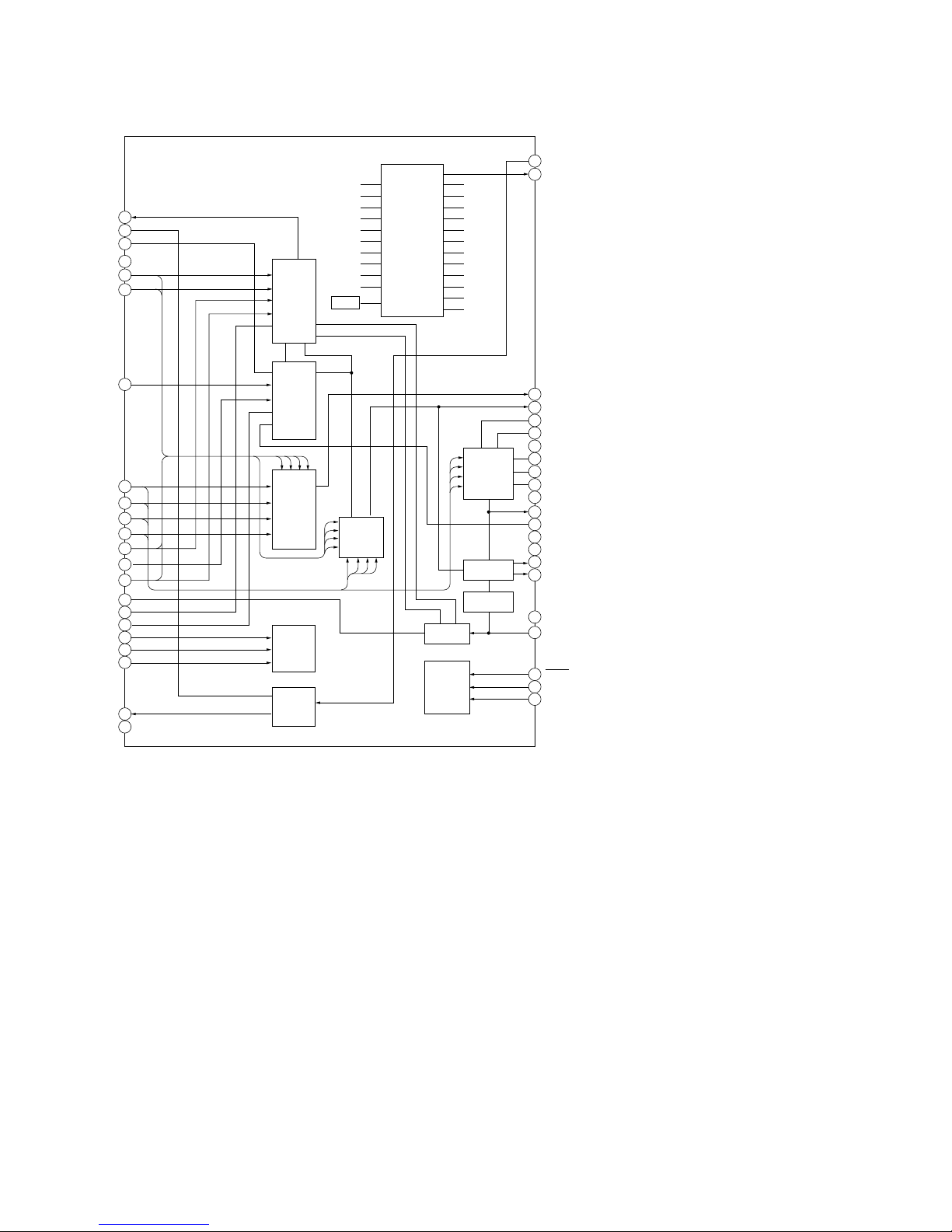
44
MZ-N707
1
TE
REXT
Wpp LPF
VREF
C
D
D-C
Iy
Ix
Jx
Jy
A
A-C
B
ADIP-IN
FE
ABCD
OFC-C1
OFC-C2
PS
LP
EQ
AGND
RF
CCSL2
VC
RESET
SCK
SBUS
VREF075
PEAK
BOTM
DGND
OFTRK
S-MON
TON-C
CIG
CDN
ADFG
DVDD
PD-NI
PD-I
PD-O
43
44
TWpp
PK/BTM
Aw
CSLO
VREF075
A-C
D-C
Malfa
Mij
AwBPF
Dw
DwBPF
42
39
AVCC
38
37
36
35
34
31
30
29
28
27
26
25
24
23
40
41
2
3
4
5
6
7
8
9
10
11
12
13
14
15
16
17
18
19
20
21
22
A+B+C+D
I+J
NPP
TON
CSL
Aw+Dw
TON Peak
TON Botm
ADIP
TE
TEMP
33
32
S-MONITOR
TE
RF
FE
APC
ADIP
T-ON
SERIAL
I/F
PEAK/BOTM
OF TRK
ABCD
Tpp/Wpp
IC501 SN761057A
Page 45
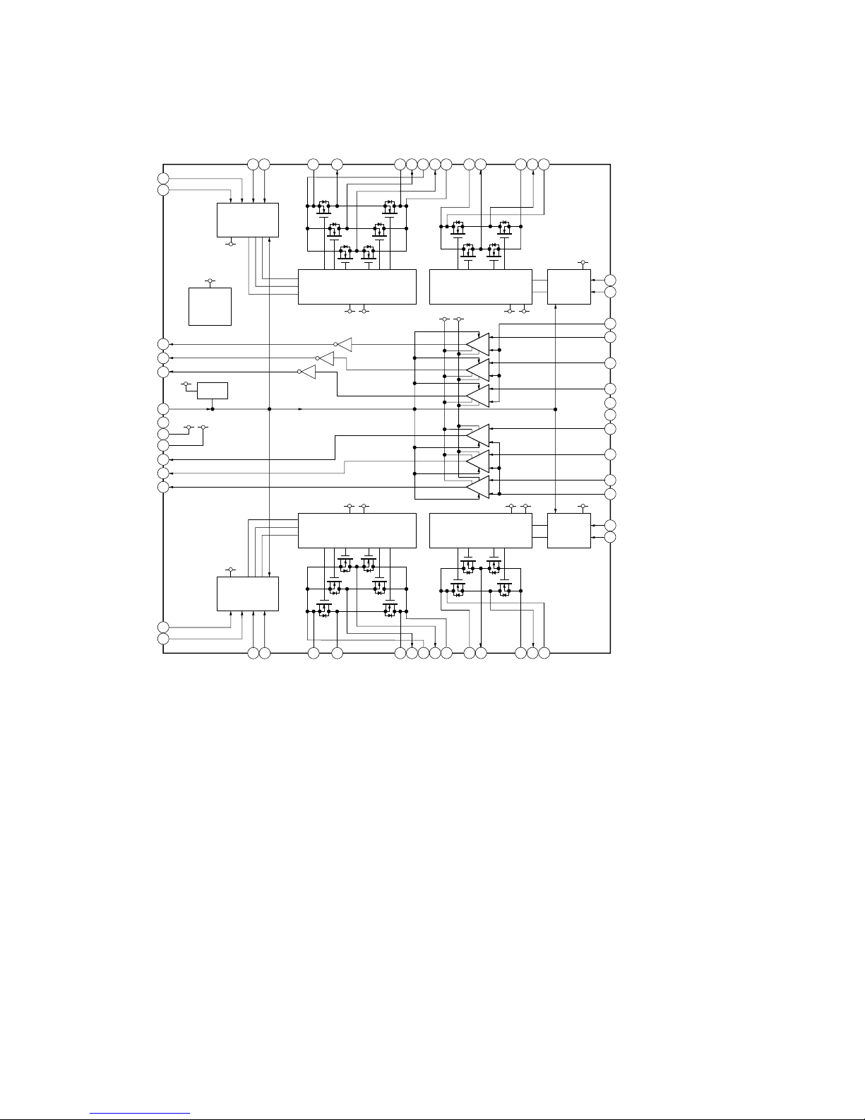
45
MZ-N707
IC551 SC111258FCR2
VC VG
VC
43
48
47
44
45
46
49
50
51
52
53
54
55
56
1 2 3 4 5
42 41 39 373840
6
35 34 3336 31 30 2932
8 9 107 12 13
14
15
11
26
27
28
24
23
22
21
20
25
17
16
18
19
UI2
OE
CPWO2
PWM2
CPUO2
CPVO2
GND1
VC
VG
CPWO1
CPVO1
CPUO1
PWM1
UI1
VI1
WI1
PGNDW1
WO1
VMVW1
VO1
UO1
VMU1
VMR1
PGNDUV1
PGND1
FO1
VMF1
RO1
FI1
COM2
RI2
FI2
CPVI2
CPWI2
NC
GND2
CPWI1
CPUI2
COM1
RI1
CPUI1
CPVI1
VI2
WI2
WO2
VO2
VMVW2
PGNDW2
UO2
VMU2
VMR2
PGNDUV
2
PGND2
FO2
VMF2
RO2
3PHASE
CONTROL
CH1
3PHASE
PRE DRIVER
CH1
H-BRIDGE
PRE DRIVER
CH1
H-BRIDGE
CONTROL
CH1
+
–
+
V
W
–
U
+
–
3PHASE
CONTROL
CH2
3PHASE
PRE DRIVER
CH2
H-BRIDGE
PRE DRIVER
CH2
H-BRIDGE
CONTROL
CH2
+
–
+
V
U
–
W
+
–
BIAS
VC LOW
VOLTAGE
DETECTOR
VG
VG
VC
VC
VG
VC
VG
VC
VC
VG
VC
VG
VC
VC
VC
Page 46
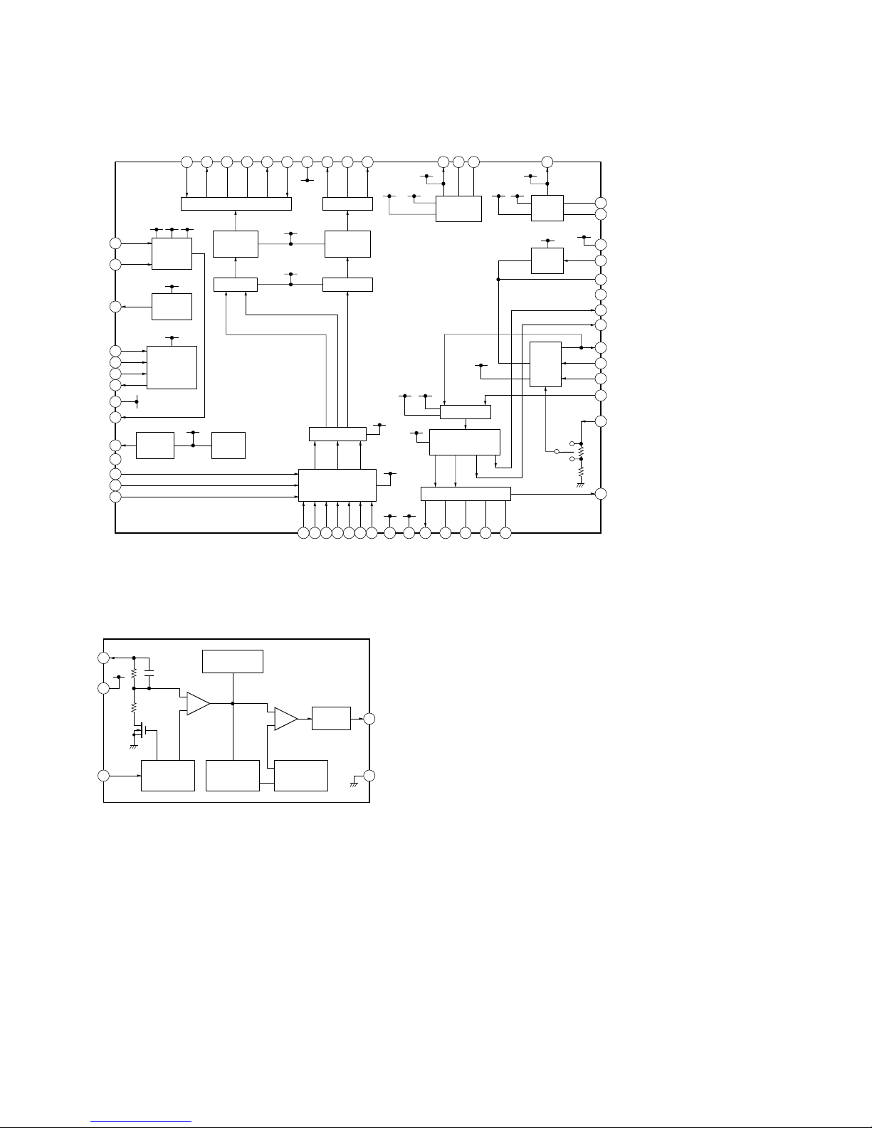
46
MZ-N707
+
–
1
2
3
+
–
VREF WITH
SOFT START,
CE
RAMP WAVE
GENERATOR,
OSC
PWM/PFM
CONTROLLER
PHASE
COMPENSATION
BUFFER,
DRIVER
5
4
VOUT
VDD
CE
GND
EXT
ERROR
AMP
PWM
COMPARATOR
IC601 XPC18A22AFCR2
IC702 XC6367A361MR
2930313233343536373839404142
43
44
45
46
47
48
49
50
51
52
54
55
56
1532 3 4 5 6 7 8 9 10 11 12 13 14
15
16
17
18
19
20
21
22
24
23
25
26
27
28
VB
BATM
CHGSW
RS
INP2
INM2
RF2
DCIN
CHGMON
SVREF
GAIN
CHG
DREG
GND
SW
RECON
OE
CLK
RI
FI
EFM
VIO
VC
RECO1
LI1
PGND1
PGND1
LI1
VRECO2
VREC
DTC
INP1
INM1
RF1
DW TP
DW BT
CVREF
GND
VREF
VC2
C1L
C1H
VG2
C2L
C2H
VG3
HA
PGND3
HB
VG
VRECIN
2
OUTB
PGND2
PGND2
OUTA
VRECIN1
OUTPUT SW
CONTROL
OUTPUT SW
CONTROL
PWM
SYSTEM
OUTPUT SW
CHARGE
CONTROL
DC IN
DETECT
DC IN
BANDGAP
HI-BRIDGE
PRE DRIVER
EFM
PRE DRIVER
CHARGE
PUMP 2
CHARGE
PUMP 1
VREF
BUFFER
SET-UP DOWN
PRE DRIVER
LEVEL
SHIFT
VC AMP
CHARGE
MONITOR
X2/X4
BATTERY
CHARGER
&
REGULATOR
VC VG DC IN
DC IN
DC IN
DC IN
DC IN
VIO
VIO VC
VC
VC
VC
VC2
VC2 VG
VC
VG
VG2
SW
VG2
VG3
VG3VG2
VG
VC
VG3
Page 47
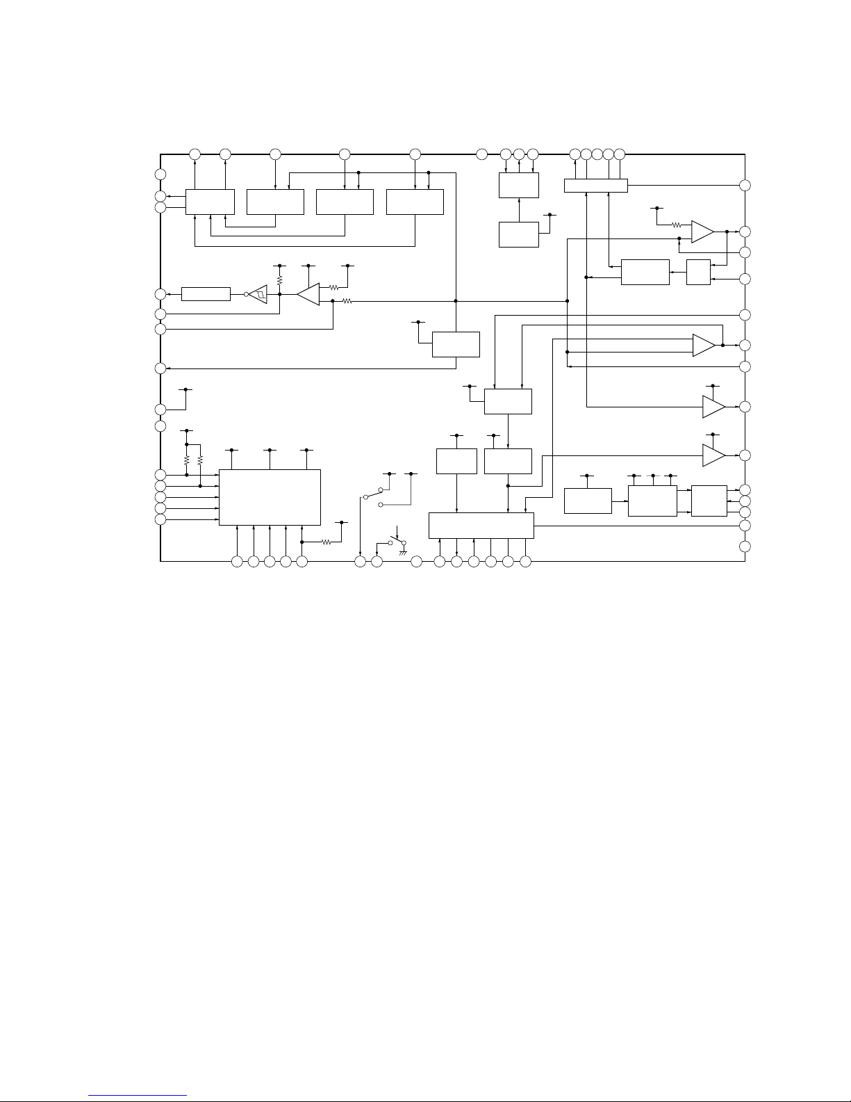
47
MZ-N707
IC901 XPC18A32FCR2
42 41 40 39 38 36 35 34 33 32 31 30 2937
28
27
26
25
24
23
22
21
20
19
18
17
16
15
1413121110987654321
56
55
54
53
52
51
50
49
48
47
46
45
44
43
+
–
+
–
CLK
SLEEP
FFCLR
VAIFON
CLKSEL
GND
VB
VREF
RSTREF
CRST
XRST
VC2
VD
NC
GND2
GND2
L2
VL
VLO
VL
GND
VRMC
VSTB
XWK4
XWK3
XWK2
XWK1
VLON
L1
RF1
INM1
DTC1
DTC2
RF2
INM2
PWM1
PWM2
VG
LG
PGND2
L2
NC
VIF
VA
VAFB
VDFB
VIFFB
VC
VCO
VC
VC OUTL1NC
PGND1
PGND1
GND
SERIES PASS
REGULATOR VA
SERIES PASS
REGULATOR VD
POWER
SWITCH 2
STEP-UP
PRE DRIVER
STEP-UP
PRE DRIVER
POWER
SWITCH 1
OUTPUT
SW
PWM
START-UP
PWM
OUTPUT SW
SERIES PASS
REGULATOR VIF
BANDGAP
REFERENCE
OUTPUT SW
SYSTEM
CONTROL
STEP-UP
DC/DC
CONVERTER
OUTPUT
SW
OUTPUT SW
OUTPUT SW
VC VC VC
VC
VC
VC
VSTB
VSTB
VB
VG
VG
VB VB VC VG
VG
VG
VC
VB
VG
VC
FFCLR
VB VC
Page 48
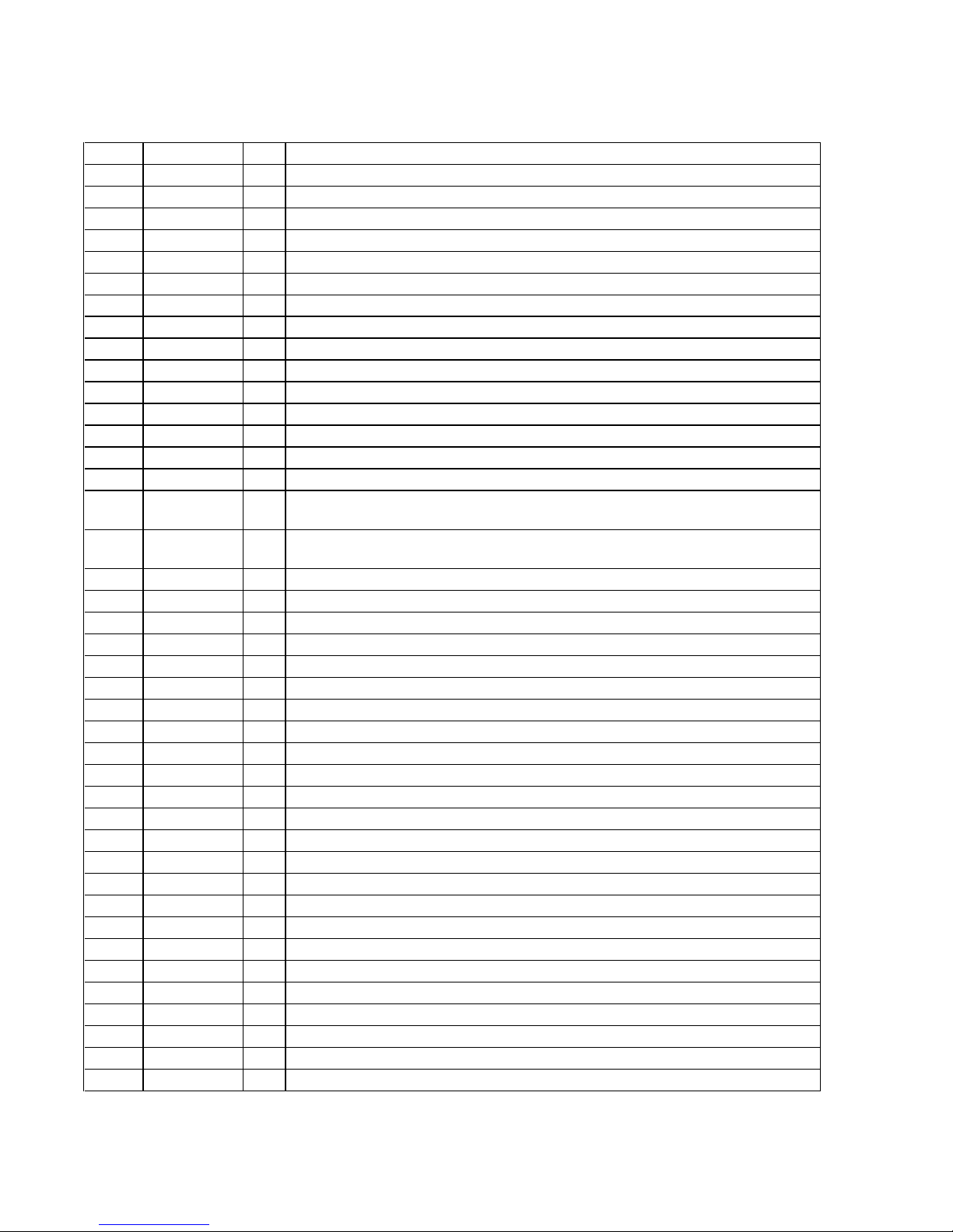
48
MZ-N707
6-11. IC PIN FUNCTION DESCRIPTION
• IC501 SN761057A (RF AMP, FOCUS/TRACKING ERROR AMP)
Pin No. Pin Name I/O Description
1 TE O Tracking error signal output to the system controller
2 REXT — Connect terminal to the external resistor for the ADIP amplifier control
3 WPP-LPF — Connect terminal to the external capacitor for the TPP/WPP low-pass filter
4 VREF O Reference voltage output terminal
5 C I Signal (C) input from the optical pickup detector
6 D I Signal (D) input from the optical pickup detector
7 D-C I Signal (D) input from the optical pickup detector (AC input)
8 IY I I-V converted RF signal (IY) input from the optical pickup detector
9 IX I I-V converted RF signal (IX) input from the optical pickup detector
10 JX I I-V converted RF signal (JX) input from the optical pickup detector
11 JY I I-V converted RF signal (JY) input from the optical pickup detector
12 A I Signal (A) input from the optical pickup detector
13 A-C I Signal (A) input from the optical pickup detector (AC input)
14 B I Signal (B) input from the optical pickup detector
15 TON-C — Connect terminal to the external capacitor for TON hold
16 CIG —
Connect terminal to the external capacitor for the low-pass filter of NPP divider
denominator
17 CDN —
Connect terminal to the external capacitor for the low-pass filter of CSL divider
denominator
18 PD-NI I Light amount monitor input terminal (non-invert input)
19 PD-I I Reference PWM signal input for the laser automatic power control from the system controller
20 PD-O O Light amount monitor output terminal
21 ADFG O ADIP duplex FM signal (22.05kHz ± 1kHz) output to the system controller
22 DVDD — Power supply terminal (+2.3V) (digital system)
23 SBUS I/O SSB serial data input/output with the system controller
24 SCK I SSB serial clock signal input from the system controller
25 XRST I Reset signal input from the system controller “L”: reset
26 OFTRK I Off track signal input terminal Not used
27 DGND — Ground terminal (digital system)
28 BOTM O Bottom hold signal output of the light amount signal (RF/ABCD) to the system controller
29 PEAK O Peak hold signal output of the light amount signal (RF/ABCD) to the system controller
30 VREF075 — Connect terminal to the external capacitor for the internal reference voltage
31 VC O Middle point voltage (+1.2V) generation output terminal
32 CCSL2 — Connect terminal to the external capacitor for the TPP/WPP low-pass filter
33 RF OUT O Playback EFM RF signal output to the system controller
34 AGND — Ground terminal (analog system)
35 to 37 EQ, LP, PS — Connect terminal to the external capacitor for the RF equalizer
38 AVCC — Power supply terminal (+2.3V) (analog system)
39, 40 OFC-2, OFC-1 — Connect terminal to the external capacitor for the RF AC coupling
41 ABCD O Light amount signal (ABCD) output to the system controller
42 FE O Focus error signal output to the system controller
43 S-MON O Servo signal monitor output to the system controller
44 ADIP-IN I ADIP duplex FM signal (22.05kHz ± 1kHz) input terminal Not used
Page 49
49
MZ-N707
• IC801 CXD2677-202GA (SYSTEM CONTROLLER, DIGITAL SIGNAL PROCESSOR, 16M BIT D-RAM)
Pin No.
Pin Name
I/O Description
1
NC
O
Load address strobe signal output terminal for D-RAM Not used
2
NC
I
Test input terminal for D-RAM Not used
3 to 7
NC
O
Address signal output terminal for D-RAM Not used
8, 9
NC
I/O
Two-way data bus terminal for D-RAM Not used
10, 11
DRAMVDD0, 1
—
Power supply terminal (for D-RAM) (+2.4V)
12, 13
DRAMVSS0, 1
—
Ground terminal (for D-RAM)
14, 15
NC
I/O
Two-way data bus terminal for D-RAM Not used
16 to 19
NC
O
Address signal output terminal for D-RAM Not used
20
NC
O
Column address strobe signal output terminal for D-RAM Not used
21
NC
I
Test input terminal for D-RAM Not used
22, 23
NC
O
Address signal output terminal for D-RAM Not used
24
DVSS0
—
Ground terminal (for the DSP block)
25
DVDD0
—
Power supply terminal (for the DSP block) (+1.5V)
26
OFTRK
I
Off track signal input from the DSP monitor (3)
27
SSB DATA I/O SSB data input/output with the RF amplifier and the remote commander attached headphone
28
SSB CLK O SSB clock output to the RF amplifier
29
VREC PWM O
PWM signal output for the Over write head drive power supply voltage control to the power
control
30
VL PWM O PWM signal output for the laser power supply voltage control to the power control
31
VC PWM O PWM signal output for the system power supply voltage control to the power control
32
NC (VD PWM) O VD power supply voltage control signal output terminal Not used
33
NC
—
Not used
34
IFVDD0
—
Power supply terminal (for the microcomputer I/F block) (+2.3V)
35
IFVSS0
—
Ground terminal (for the microcomputer I/F block)
36
OPT DET I DIN plug detection signal input terminal “H”: DIN plug
37
XJACK DET I LINE IN plug detection signal input terminal “L”: LINE or OPT plug
38
XMIC DET I Microphone plug detection signal input terminal “L”: microphone plug
39
OPEN CLOSE
SW
I
Open/close detection switch of the upper panel input terminal
“L”: when upper panel close
40, 41
SET CODE0, 1 I Input terminal for the set (open in this set)
42, 43
SET CODE2, 3 I Input terminal for the set (fixed at “L” in this set)
44
XPATCH I Patch function detection signal input terminal “L”: patch function Not used
45
SI0 I Serial data input from the nonvolatile memory
46
SO0 O
Serial data output to the nonvolatile memory, A/D converter and liquid crystal display element
module
47
SCK0 O
Serial clock signal output to the nonvolatile memory, A/D converter and liquid crystal display
element module
48
XGUM ON I
Rechargeable battery detection switch input terminal “L”: there is rechargeable battery
Not used
49
BEEP O Beep sound control signal output to the headphone amplifier
50, 51
TEST1, TEST0 I Input terminal for the main test (normally fixed at “L”)
52
KDO
O
Data output terminal Not used
53
KRB
I
Ready/busy signal input terminal Not used
54
KCLK
O
Clock signal output terminal Not used
55
KCS
O
Chip select signal output terminal Not used
56
KDI
I
Data input terminal Not used
Page 50

50
MZ-N707
Pin No.
Pin Name
I/O Description
57
TRST
I
Input terminal for the test mode set (normally fixed at “L”)
58
XOPT CTL O Power supply ON/OFF control signal output for the DIN PD drive
59
VG CTL O VG power supply voltage control signal output terminal Not used
60
AOUT SEL O HP/LINE changeover signal output terminal Not used
61
REC OPR LED O LED ON/OFF control signal output terminal Not used
62
TSB SSB CTL O TSB/SSB changeover control signal output Not used
63
GND SW2 O Battery for Cradle ON/OFF switch control signal output terminal Not used
64
CLK SEL O System clock select signal output to the power control
65 MIC SENSE O
Mic sensitivity control signal output to the mic amplifier
“L”: Low sensitivity “H”: High sensitivity (normally: “H”) Not used
66 GND SW O GND changeover control signal output terminal
67 XCS LCD O Chip select signal output to the liquid crystal display element module
68 LCD STB O Strobe signal output to the liquid crystal display element module
69 MUTE O Analog muting control signal output for the headphone amplifier “H”: muting ON
70 CS RTC O Chip select signal output terminal Not used
71 XCS NV1 O Chip select signal (1) output to the nonvolatile memory
72 IFVDD1
—
Power supply terminal (for the microcomputer I/F block) (+2.3V)
73 IFVSS1
—
Ground terminal (for the microcomputer I/F block)
74
XRST MTR
DRV
O Reset control signal output to the motor driver “L”: reset
75 XRF RST O Reset control signal output to the RF amplifier “L”: reset
76 SPDL MON I Spindle servo monitor signal input terminal
77 XHOLD SW I HOLD switch input terminal “L”: hold ON
78, 79 JOG A, B I Jog dial pulse input terminal Not used
80, 81 PD S0, PD S1 O PD IC mode changeover signal output to the optical pick up
82 PAUSE KEY I Pause key input terminal from the switch & liquid crystal display element module
83 PROTECT I Detection input terminal of the record check claw from the protect detection switch “H”: protect
84 SLD MON I Sled servo monitor signal input terminal
85 VLON O Power supply control signal output for the laser diode drive to the power control
86 DVSS1
—
Ground terminal (for the DSP block)
87 DVDD1
—
Power supply terminal (for the DSP block) (+1.5V)
88 SLEEP O System sleep control signal output to the power control “H”: sleep ON
89 FFCLR O Input latch output for the start switching to the power control
90 CHG GAIN O Charge gain control signal output to the power control
91 CHG CTL O Charge ON/OFF control signal output to the power control “H”: charge ON
92 CHGI CTL O Charge current control signal output terminal Not used
93 XHP STBY
O
Power supply control signal output for the head phone
94 XCS NV2 O Chip select signal (2) output terminal Not used
95 IFVSS2
—
Ground terminal (for the microcomputer I/F block)
96 IFVDD2
—
Power supply terminal (for the microcomputer I/F block) (+2.3V)
97 T MARK SW I T MARK (track mark) switch input terminal “L”: track mark detection Not used
98 NC O LED ON/OFF control signal output terminal for CHG (charge display) Not used
99 NC I Initial switch detection input terminal Not used
100 NC
—
Not used
101 XUDP UP ON O Pullup resistor changeover control signal output terminal Not used
102 LCD RST O Reset control signal output to the liquid crystal display element module “L”: reset
103 XMUTE O Analog muting control signal output terminal “L”: muting ON Not used
Page 51

51
MZ-N707
Pin No.
Pin Name
I/O Description
104 XRST
I
System reset signal input from the power control “L”: reset
105 STAND DET I Charging stand detection signal input terminal
106 VB MON
I
Voltage monitor input terminal (A/D input) of the UNREG power supply
107 CHG MON
I
Charge voltage monitor input (A/D input) from the power control
108 VREF MON I Clear reference voltage monitor input terminal (A/D input) from the RF amplifier
109, 110 SET KEY 1, 2 I Key input terminal (A/D input) from the switch & liquid crystal display element module
111 VBUS DET I USB power supply voltage detection signal input terminal
112 HIDC MON
I
HIGH DC voltage monitor input terminal (A/D input)
113 WK DET
I
Set key and USB start switching detection signal input terminal (A/D input)
114 REC KEY
I
REC key input terminal (A/D input)
115
HALF LOCK
SW
I
Open button detection switch input terminal (A/D input)
Input “L” when the open button is pressed. Input “H” in other cases.
116 RMC KEY
I
Key input terminal (A/D input) from the remote commander attached headphone
117 AVDD
—
Power supply terminal (for the microcomputer analog) (+2.8V)
118 AVSS
—
Ground terminal (for the microcomputer analog)
119 TSMVDD
—
Power supply terminal (for the TSB master communication) (+2.8V)
120 RMC DTCK I/O Serial data input/output with the remote commander attached headphone
121 TSLVDD
—
Power supply terminal (for the I/F to TSB slave) (+2.3V)
122, 123 NC
—
Not used
124 TAT
—
Not used
125 TAN
—
Not used
126 NAR
—
Not used
127 ID0
—
Not used
128 SAK
—
Not used
129 IT0
—
Not used
130 MITY
—
Ground terminal Not used
131 SUSPEND
O
USB suspend signal output terminal
132 USBIFVDD
—
Power supply terminal (for USB I/F) (+3.3V)
133 UDM I USB data (-) input terminal
134 UDP I USB data (+) input terminal
135 UPUEN O USB pullup resistor connection control output terminal
136 USBOSCVDD
—
Power supply terminal (for the USB oscillation circuit) (+2.4V)
137 UOSCI I Clock (48MHz) input terminal for the USB
138 UOSCO O Clock (48MHz) output terminal for the USB
139 USBOSCVSS
—
Ground terminal (for the USB oscillation circuit)
140 to
142
MODE1 to 3 O Power supply control signal output for the over write head to the over write head drive
143 HD CON 1 O Over write head control signal output to the over write head drive
144 PBVDD
—
Power supply terminal (+2.3V)
145 HD CON 2 O Over write head control signal output to the over write head drive
146 XTEST I Input terminal for test mode set (normally: open) “L”: test mode
147 XCS ADA O Chip select signal output to the A/D converter
148 XPD ADA O Power supply control signal output for the drive to the A/D converter
149 VDIOSC
—
Power supply terminal (for the OSC cell) (+2.4V)
150 OSCI
I
System clock (45.1584MHz) input terminal
151 OSCO
O
System clock (45.1584MHz) output terminal
152 VSIOSC — Ground terminal (for the OSC cell)
Page 52

52
MZ-N707
Pin No.
Pin Name
I/O Description
153 DAVDD
—
Power supply terminal (for the built-in D/A converter) (+2.4V)
154 VREFL I Reference voltage input terminal (for the built-in D/A converter L-CH)
155 AOUTL
O
Built-in D/A converter (L-CH) output terminal
156 AOUTR
O
Built-in D/A converter (R-CH) output terminal
157 VREFR
I
Reference voltage input terminal (for the built-in D/A converter R-CH)
158 DAVSS
—
Ground terminal (for the built-in D/A converter)
159 ASYO
O
Playback EFM duplex signal output terminal
160 ASYI I Playback EFM comparison slice level input terminal
161 AVD1
—
Power supply terminal (for the DSP asymmetry system analog) (+2.4V)
162 BIAS
I
Bias current input terminal for the playback EFM comparison
163 RFI
I
Playback EFM the RF signal input from the RF amplifier
164 AVS1
—
Ground terminal (for the DSP asymmetry system analog)
165 PCO O Phase comparison output terminal for the playback EFM system master PLL
166 FILI
I
Filter input terminal for the playback EFM system master PLL
167 FILO O Filter output terminal for the playback EFM system master PLL
168 CLTV I Internal VCO control voltage input terminal for the playback EFM system master PLL
169 PEAK
I
Peak hold signal input of the light amount signal (RF/ABCD) from the RF amplifier
170 BOTM
I
Bottom hold signal input of the light amount signal (RF/ABCD) from the RF amplifier
171 ABCD I Light amount signal (ABCD) input from the RF amplifier
172 FE I Focus error signal input from the Focus error amplifier
173 AUX1 I Support signal (I
3
signal/temperature signal) input terminal (A/D input)
174 VC I Middle point voltage (+1.1V) input terminal
175 ADIO O Monitor output terminal of A/D converter input signal Not used
176 ADRT I A/D converter the upper limit voltage input terminal (fixed at “H” in this set)
177 AVD2
—
Power supply terminal (for the DSP servo analog system) (+2.4V)
178 AVS2
—
Ground terminal (for the DSP servo analog system)
179 ADRB
I
A/D converter the lower limit voltage input terminal (fixed at “L” in this set)
180 SE
I
Servo signal monitor input terminal (A/D input) from the RF amplifier
181 TE
I
Tracking error signal input from the Tracking error amplifier
182 DCHG
—
Connecting terminal with the analog power supply of the low impedance (fixed at “H” in this set)
183 APC
I
Error signal input for the laser automatic power control (fixed at “H” in this set)
184 CKRF O Clock output terminal for the RF amplifier control Not used
185 DTRF O Data output terminal for the RF amplifier control Not used
186 XLRF O Latch signal output terminal for the RF amplifier control Not used
187 DVSS2
—
Ground terminal (for the DSP block)
188 DVDD2
—
Power supply terminal (for the DSP block) (+1.5V)
189 XTSL
I
Input terminal for the frequency set up of the system clock
“L”: 45.1584MHz, “H”: 22.5792MHz (fixed at “L” in this set)
190 DIN1
I
Input terminal of the record system digital audio signal
191 to
193
NC O D/A converter PWM signal output terminal Not used
194 DADT O Audio data output terminal Not used
195 ADDT
I
Data input from the external A/D converter
196 LRCK O L/R sampling clock signal (44.1KHz) output to the external A/D converter
197 XBCK O Bit clock signal (2.8224MHz) output to the external A/D converter
198 FS256
O
11.2896MHz clock signal output to the external A/D converter
199 NC
I
Ground terminal Clock signal input from the external VCO Not used
Page 53

53
MZ-N707
Pin No.
Pin Name
I/O Description
200 DVSS3
—
Ground terminal (for the DSP block)
201 DVDD3
—
Power supply terminal (for the DSP block) (+1.5V)
202 ADFG
I
ADIP duplex FM signal (20.05±1kHz) input from the RF amplifier
203 NC
O
Filter cut off control signal output terminal Not used
204 IFVDD3
—
Power supply terminal (for the microcomputer I/F block) (+2.3V)
205 IFVSS3
—
Ground terminal (for the microcomputer I/F block)
206 APCREF O Reference PWM signal output for the laser automatic power control to the RF amplifier
207 TRDR O Tracking servo drive PWM signal output (–) to the coil driver
208 TFDR O Tracking servo drive PWM signal output (+) to the coil driver
209 FFDR O Focus servo drive PWM signal output (+) to the coil driver
210 FRDR O Focus servo drive PWM signal output (–) to the coil driver
211 FS4 O 176.4kHz clock signal output to the power control
212 SPRD O Spindle motor drive control signal output (U) to the motor driver
213 SPFD O Spindle servo drive PWM signal output to the motor driver
214 SPDV O Spindle motor drive control signal output (V) to the motor driver
215 SPDW O Spindle motor drive control signal output (W) to the motor driver
216 SPCU I Spindle motor drive comparison signal input (U) from the motor driver
217 SPCV I Spindle motor drive comparison signal input (V) from the motor driver
218 SPCW I Spindle motor drive comparison signal input (W) from the motor driver
219 SRDR O Sled motor drive control signal output (U) to the motor driver
220 SFDR O Sled servo drive PWM signal output to the motor driver
221 SLDV O Sled motor drive control signal output (V) to the motor driver
222 SLDW O Sled motor drive control signal output (W) to the motor driver
223 DVSS4
—
Ground terminal (for the DSP block)
224 DVDD4
—
Power supply terminal (for the DSP block) (+1.5V)
225 SLCU I Sled motor drive comparison signal input (U) from the motor driver
226 SLCV I Sled motor drive comparison signal input (V) from the motor driver
227 SLCW I Sled motor drive comparison signal input (W) from the motor driver
228 IFVDD4
—
Power supply terminal (for the microcomputer I/F block) (+2.3V)
229 IFVSS4
—
Ground terminal (for the microcomputer I/F block)
230 EFMO O EFM encode data output for the record to the over write head drive
231 to
233
MNT0 to 2 O DSP monitor (0) to (2) output terminal Not used
234 MNT3 O Off track signal output from the DSP monitor (3)
235 SENSE O DSP internal status (DSP SENS monitor) signal output terminal Not used
236 TX O Record data output enable signal output monitor terminal of the DSP Not used
237 RECP O Laser power changeover signal output terminal Not used
238 LRCKI/XELT
I
Input terminal for the PCM data I/F/ ATRAC data I/F Not used
239 XBCKI/ECK
I
Input terminal for the PCM data I/F/ ATRAC data I/F Not used
240 DATAI/EDT
I
Input terminal for the PCM data I/F/ ATRAC data I/F Not used
241 XERQ
I
Input terminal for the ATRAC data I/F Not used
242 A11
O
Address signal output terminal for D-RAM Not used
243 XOE
O
Output enable signal output terminal for D-RAM Not used
244 XWE
O
Data write enable signal output terminal for D-RAM Not used
245 TSTDR3
I
Test input terminal for D-RAM Not used
246 EVA I
EVA/FLASH chip discrimination input terminal “L”: FLASH chip, “H”: EVA chip
(fixed at “L” in this set)
Page 54

54
MZ-N707
Pin No.
Pin Name
I/O Description
247 FLASHVDD
—
Power supply terminal (for the built-in flash memory) (+2.4V)
248 FLASHVSS
—
Ground terminal (for the built-in flash memory)
249 to
256
NC
—
Not used
Page 55
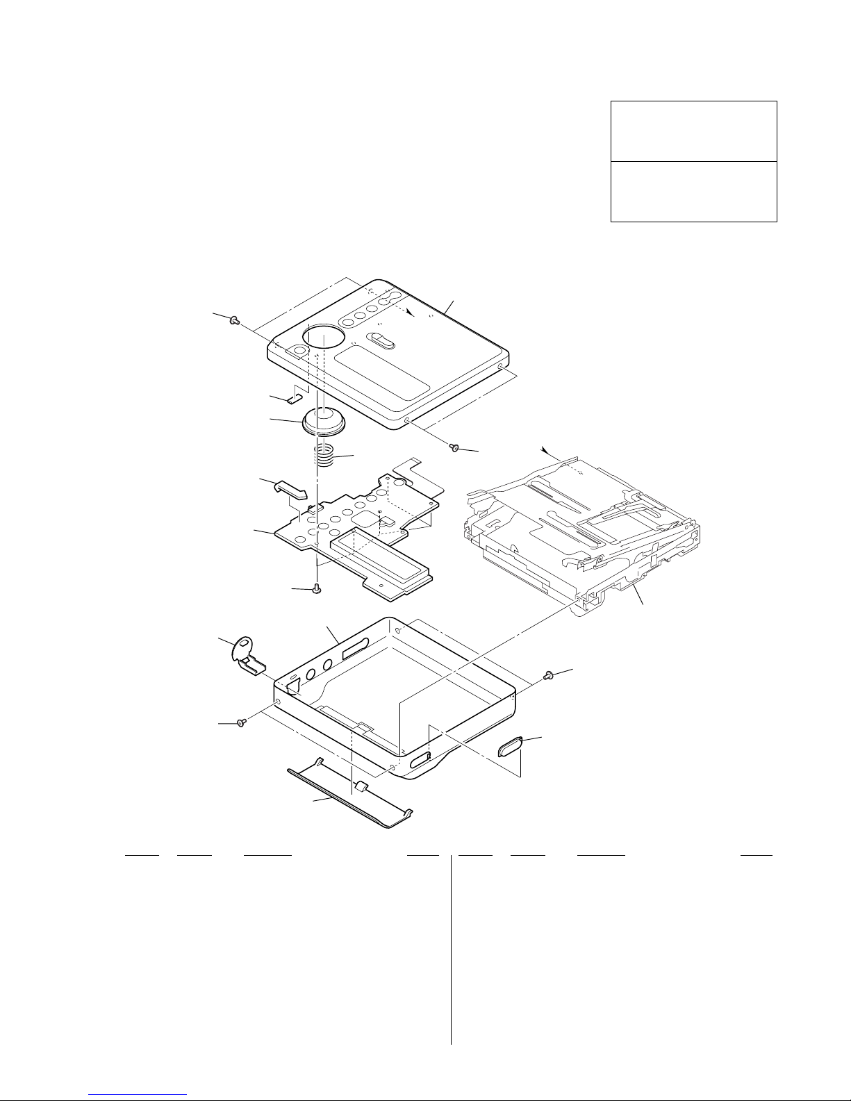
55
MZ-N707
7-1. UPPER PANEL, CASE (LOWER) SECTION
SECTION 7
EXPLODED VIEWS
• Items marked “*” are not stocked since they
are seldom required for routine service. Some
delay should be anticipated when ordering
these items.
• The mechanical parts with no reference number in the exploded views are not supplied.
• Accessories are given in the last of the electrical parts list.
NOTE:
• -XX and -X mean standardized parts, so they
may have some difference from the original
one.
• Color Indication of Appearance Parts
Example:
KNOB, BALANCE (WHITE) . . . (RED)
↑↑
Parts Color Cabinet's Color
• Abbreviation
CND: Canadian model
FR : French model
Les composants identifiés par une
marque 0 sont critiquens pour la
sécurité.
Ne les remplacer que par une pièce
portant le numéro spécifié.
The components identified by mark
0 or dotted line with mark 0 are
critical for safety.
Replace only with part number
specified.
Ref. No. Part No. Description Remark
Ref. No. Part No. Description Remark
1 X-3381-803-1 PANEL (S) SUB ASSY, UPPER (SILVER)
1 X-3381-804-1 PANEL (L) SUB ASSY, UPPER (BLUE)
1 X-3381-805-1 PANEL (B) SUB ASSY, UPPER (BLACK)
2 3-234-449-17 SCREW (M1.4) (for BLACK)
2 3-234-449-19 SCREW (M1.4) (for BLUE, SILVER)
3 3-237-094-01 SPRING (BUTTON), COMPRESSION
4 1-804-543-11 LCD MODULE
5 3-318-382-91 SCREW (1.7X2.5), TAPPING
6 3-237-098-01 CASE (LOWER) (SILVER) (AEP, UK, FR)
6 3-237-098-11 CASE (LOWER) (SILVER) (US, CND)
6 3-237-098-21 CASE (LOWER) (BLUE) (AEP, UK, FR)
6 3-237-098-31 CASE (LOWER) (BLUE) (US, CND)
6 3-237-098-41 CASE (LOWER) (BLACK) (AEP, UK, FR)
6 3-237-098-51 CASE (LOWER) (BLACK) (US, CND)
7 3-237-100-01 CAP (P) (for BLUE, SILVER)
7 3-237-100-11 CAP (P) (for BLACK)
8 3-237-099-01 BUTTON (OPEN)
9 3-225-636-21 LID, BATTERY CASE (SILVER)
9 3-225-636-31 LID, BATTERY CASE (BLUE)
9 3-225-636-41 LID, BATTERY CASE (BLACK)
10 3-238-582-01 SHEET (GROUND)
11 3-239-790-01 SPACER (UP)
12 3-237-093-01 BUTTON (CONTROL B)
chassis section
1
2
11
12
10
3
4
5
6
7
2
9
8
2
2
Page 56
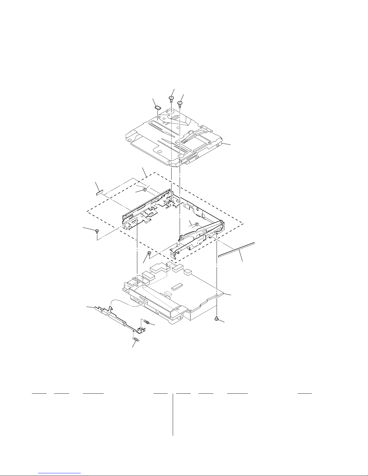
56
MZ-N707
7-2. CHASSIS SECTION
Ref. No. Part No. Description Remark
Ref. No. Part No. Description Remark
51 3-237-072-01 SCREW (MD), STEP
52 3-238-127-01 SPACER (HOLDER)
53 X-3381-652-1 CHASSIS (5192) ASSY, SET
54 3-237-075-01 SPRING (POP UP-L), TORSION
55 3-237-083-01 SPRING (POP UP-R), TORSION
56 3-239-791-01 SHEET (FULCRUM PLATE LA)
57 3-318-382-91 SCREW (1.7X2.5), TAPPING
58 3-237-080-01 SLIDER, OPEN
59 3-237-082-01 SPRING (LOCK), TENSION
60 3-237-081-01 SPRING (LIMITTER), COMPRESSION
61 3-335-797-01 SCREW (M1.4X2), TOOTHED LOCK
62 3-239-800-01 SHEET (FULCRUM PLATE RA)
MT-MZN707-177
main board sectio
n
51
51
52
53
56
62
54
57
57
58
59
60
61
55
Page 57
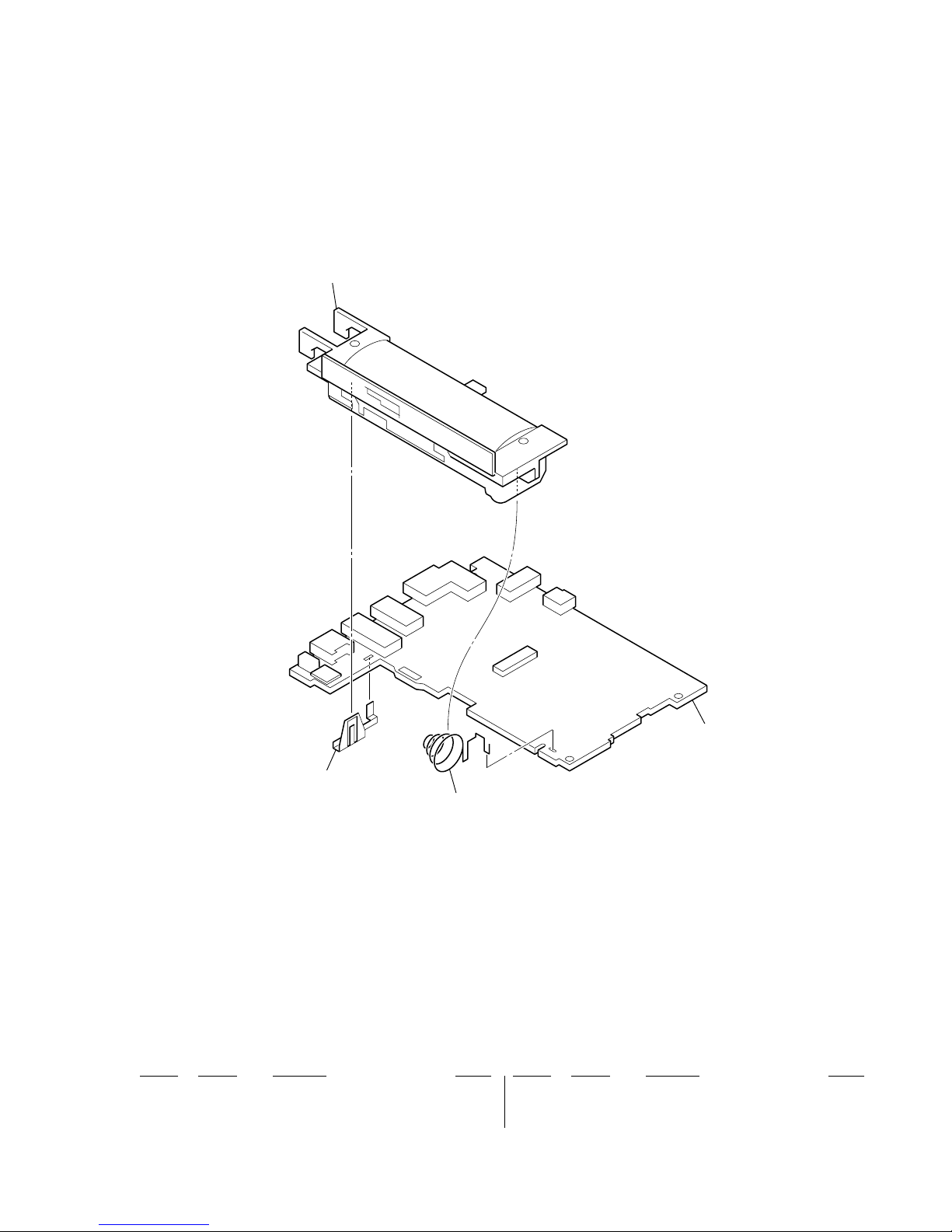
57
MZ-N707
7-3. MAIN BOARD SECTION
Ref. No. Part No. Description Remark
Ref. No. Part No. Description Remark
101 3-237-079-01 CASE, BATTERY
102 3-237-073-01 TERMINAL BOARD (+), BATTERY
103 3-237-074-01 TERMINAL (–), BATTERY
* 104 X-3381-933-1 MAIN BOARD, COMPLETE (EXCEPT US, FR)
* 104 X-3381-967-1 MAIN BOARD, COMPLETE (US)
* 104 X-3382-202-1 MAIN BOARD, COMPLETE (FR)
101
102
103
104
Page 58
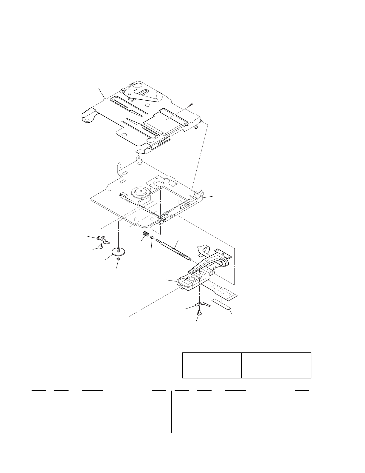
58
MZ-N707
7-4. MECHANISM DECK SECTION-1
(MT-MZN707-177)
The components identified by
mark 0 or dotted line with
mark 0 are critical for safety .
Replace only with part number specified.
Les composants identifiés par une
marque 0 sont critiques pour la
sécurité.
Ne les remplacer que par une pièce
portant le numéro spécifié.
Ref. No. Part No. Description Remark
Ref. No. Part No. Description Remark
301 X-3381-219-1 HOLDER ASSY
302 3-224-779-02 SPRING, THRUST DETENT
303 3-225-996-01 SCREW (M1.4) (EG), PRECISION PAN
304 4-222-216-01 GEAR (SA)
305 3-338-645-31 WASHER (0.8-2.5)
306 4-222-208-01 GEAR (SB)
307 3-043-237-02 BEARING (N)
308 4-222-203-02 SCREW, LEAD
0 309 X-3381-589-1 SERVICE ASSY, OP (LCX-5R)
310 3-049-336-03 SPRING (S), RACK
311 3-225-996-06 SCREW (M1.4) (EG), PRECISION PAN
mechanism deck section-
2
301
not supplied
311
310
309
308
307
305
304
303
302
306
Page 59
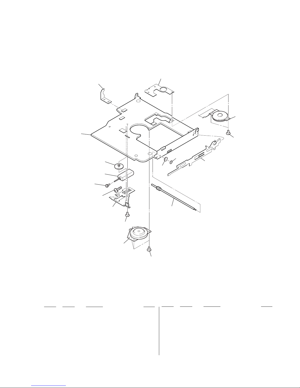
59
MZ-N707
7-5. MECHANISM DECK SECTION-2
(MT-MZN707-177)
Ref. No. Part No. Description Remark
Ref. No. Part No. Description Remark
351 3-225-278-11 SCREW, TAPPING
352 3-235-838-01 COVER, MOTOR
353 3-235-836-01 GEAR (HB)
354 3-222-544-01 GEAR (HA)
355 3-235-835-01 GEAR (HC)
356 3-235-834-01 CHASSIS
357 3-235-830-01 PLATE, RATCHET
358 X-3379-529-4 BASE ASSY, MOTOR
359 3-225-996-07 SCREW (M1.4) (EG), PRECISION PAN
360 3-235-839-01 LEVER (RACK)
361 3-338-645-31 WASHER (0.8-2.5)
362 4-222-222-01 GEAR (RACK)
363 A-3174-089-A SHAFT BLOCK ASSY, SUB
M601 8-835-744-01 MOTOR, DC SSM18B (SPINDLE)
(WITH TURN TABLE)
M602 1-763-727-11 MOTOR, DC (SLED) (WITH GEAR)
M603 1-763-400-21 MOTOR, DC (OVER WRITE HEAD UP/DOWN)
M601
M603
351
351
363
362
361
360
359
352
353
354
355
356
357
358
M60
2
Page 60

60
MZ-N707
SECTION 8
ELECTRICAL PARTS LIST
Ref. No. Part No. Description Remark Ref. No. Part No. Description Remark
MAIN
* X-3381-933-1 MAIN BOARD, COMPLETE (EXCEPT US, FR)
* X-3381-967-1 MAIN BOARD, COMPLETE (US)
* X-3382-202-1 MAIN BOARD, COMPLETE (FR)
*********************
< CAPACITOR >
C101 1-107-823-11 CERAMIC CHIP 0.47uF 10% 16V
(US)
C101 1-125-889-11 CERAMIC CHIP 2.2uF 10% 10V
(EXCEPT US)
C102 1-164-941-11 CERAMIC CHIP 0.0047uF 10% 16V
C103 1-164-939-11 CERAMIC CHIP 0.0022uF 10% 50V
C104 1-135-868-11 TANTALUM CHIP 220uF 20% 2.5V
C105 1-115-467-11 CERAMIC CHIP 0.22uF 10% 10V
C106 1-164-937-11 CERAMIC CHIP 0.001uF 10% 50V
C110 1-125-837-11 CERAMIC CHIP 1uF 10% 6.3V
C111 1-164-874-11 CERAMIC CHIP 100PF 5% 50V
C112 1-125-837-11 CERAMIC CHIP 1uF 10% 6.3V
C113 1-131-862-11 TANTALUM CHIP 47uF 20% 4V
C116 1-164-937-11 CERAMIC CHIP 0.001uF 10% 50V
C117 1-125-891-11 CERAMIC CHIP 0.47uF 10% 10V
C118 1-164-939-11 CERAMIC CHIP 0.0022uF 10% 50V
C201 1-107-823-11 CERAMIC CHIP 0.47uF 10% 16V
(US)
C201 1-125-889-11 CERAMIC CHIP 2.2uF 10% 10V
(EXCEPT US)
C202 1-164-941-11 CERAMIC CHIP 0.0047uF 10% 16V
C203 1-164-939-11 CERAMIC CHIP 0.0022uF 10% 50V
C204 1-135-868-11 TANTALUM CHIP 220uF 20% 2.5V
C205 1-115-467-11 CERAMIC CHIP 0.22uF 10% 10V
C206 1-164-937-11 CERAMIC CHIP 0.001uF 10% 50V
C210 1-125-837-11 CERAMIC CHIP 1uF 10% 6.3V
C211 1-164-874-11 CERAMIC CHIP 100PF 5% 50V
C212 1-125-837-11 CERAMIC CHIP 1uF 10% 6.3V
C213 1-131-862-11 TANTALUM CHIP 47uF 20% 4V
C216 1-164-937-11 CERAMIC CHIP 0.001uF 10% 50V
C217 1-125-891-11 CERAMIC CHIP 0.47uF 10% 10V
C218 1-164-939-11 CERAMIC CHIP 0.0022uF 10% 50V
C301 1-110-569-11 TANTALUM CHIP 47uF 20% 6.3V
C302 1-107-820-11 CERAMIC CHIP 0.1uF 16V
C305 1-135-149-21 TANTALUM CHIP 2.2uF 20% 10V
C306 1-107-820-11 CERAMIC CHIP 0.1uF 16V
C307 1-125-777-11 CERAMIC CHIP 0.1uF 10% 10V
C308 1-125-777-11 CERAMIC CHIP 0.1uF 10% 10V
C309 1-119-923-11 CERAMIC CHIP 0.047uF 10% 10V
NOTE:
• Due to standardization, replacements in the
parts list may be different from the parts specified in the diagrams or the components used
on the set.
• -XX and -X mean standardized parts, so they
may have some difference from the original
one.
• RESISTORS
All resistors are in ohms.
METAL: Metal-film resistor.
METAL OXIDE: Metal oxide-film resistor.
F: nonflammable
• Items marked “*” are not stocked since they
are seldom required for routine service.
Some delay should be anticipated when ordering these items.
• SEMICONDUCTORS
In each case, u: µ, for example:
uA. . : µA. . uPA. . : µPA. .
uPB. . : µPB. . uPC. . : µPC. .
uPD. . : µPD. .
• CAPACITORS
uF: µF
• COILS
uH: µH
C310 1-164-937-11 CERAMIC CHIP 0.001uF 10% 50V
C311 1-125-777-11 CERAMIC CHIP 0.1uF 10% 10V
C312 1-125-889-11 CERAMIC CHIP 2.2uF 10% 10V
C314 1-135-259-11 TANTALUM CHIP 10uF 20% 6.3V
C315 1-125-837-11 CERAMIC CHIP 1uF 10% 6.3V
C316 1-135-201-11 TANTALUM CHIP 10uF 20% 4V
C317 1-119-750-11 TANTALUM CHIP 22uF 20% 6.3V
C318 1-110-569-11 TANTALUM CHIP 47uF 20% 6.3V
C319 1-164-943-11 CERAMIC CHIP 0.01uF 10% 16V
C320 1-135-151-21 TANTALUM CHIP 4.7uF 20% 4V
C321 1-125-777-11 CERAMIC CHIP 0.1uF 10% 10V
C322 1-110-569-11 TANTALUM CHIP 47uF 20% 6.3V
C323 1-135-259-11 TANTALUM CHIP 10uF 20% 6.3V
C324 1-135-259-11 TANTALUM CHIP 10uF 20% 6.3V
C325 1-164-937-11 CERAMIC CHIP 0.001uF 10% 50V
C326 1-164-937-11 CERAMIC CHIP 0.001uF 10% 50V
C327 1-164-937-11 CERAMIC CHIP 0.001uF 10% 50V
C330 1-107-820-11 CERAMIC CHIP 0.1uF 16V
C331 1-164-937-11 CERAMIC CHIP 0.001uF 10% 50V
C332 1-135-259-11 TANTALUM CHIP 10uF 20% 6.3V
C334 1-125-777-11 CERAMIC CHIP 0.1uF 10% 10V
C335 1-135-259-11 TANTALUM CHIP 10uF 20% 6.3V
C336 1-164-933-11 CERAMIC CHIP 220PF 10% 50V
C340 1-125-777-11 CERAMIC CHIP 0.1uF 10% 10V
C501 1-164-874-11 CERAMIC CHIP 100PF 5% 50V
C502 1-107-819-11 CERAMIC CHIP 0.022uF 10% 16V
C503 1-164-939-11 CERAMIC CHIP 0.0022uF 10% 50V
C504 1-164-939-11 CERAMIC CHIP 0.0022uF 10% 50V
C505 1-164-943-11 CERAMIC CHIP 0.01uF 10% 16V
C506 1-107-819-11 CERAMIC CHIP 0.022uF 10% 16V
C507 1-107-819-11 CERAMIC CHIP 0.022uF 10% 16V
C508 1-125-777-11 CERAMIC CHIP 0.1uF 10% 10V
C509 1-164-939-11 CERAMIC CHIP 0.0022uF 10% 50V
C510 1-164-850-11 CERAMIC CHIP 10PF 0.5PF 50V
C511 1-164-850-11 CERAMIC CHIP 10PF 0.5PF 50V
C512 1-125-777-11 CERAMIC CHIP 0.1uF 10% 10V
C513 1-164-850-11 CERAMIC CHIP 10PF 0.5PF 50V
C514 1-107-819-11 CERAMIC CHIP 0.022uF 10% 16V
C515 1-125-777-11 CERAMIC CHIP 0.1uF 10% 10V
C516 1-125-777-11 CERAMIC CHIP 0.1uF 10% 10V
C518 1-127-760-11 CERAMIC CHIP 4.7uF 10% 6.3V
C519 1-164-941-11 CERAMIC CHIP 0.0047uF 10% 16V
C521 1-125-777-11 CERAMIC CHIP 0.1uF 10% 10V
• Abbreviation
CND: Canadian model
FR : French model
Les composants identifiés par une
marque 0 sont critiquens pour la
sécurité.
Ne les remplacer que par une pièce
portant le numéro spécifié.
The components identified by
mark 0 or dotted line with mark
0 are critical for safety.
Replace only with part number
specified.
When indicating parts by reference
number, please include the board.
Page 61

Ref. No. Part No. Description Remark
Ref. No. Part No. Description Remark
61
MZ-N707
C522 1-125-777-11 CERAMIC CHIP 0.1uF 10% 10V
C523 1-125-837-11 CERAMIC CHIP 1uF 10% 6.3V
C524 1-135-259-11 TANTALUM CHIP 10uF 20% 6.3V
C527 1-119-923-11 CERAMIC CHIP 0.047uF 10% 10V
C529 1-165-851-11 TANTALUM CHIP 10uF 20% 6.3V
C530 1-164-939-11 CERAMIC CHIP 0.0022uF 10% 50V
C531 1-164-943-11 CERAMIC CHIP 0.01uF 10% 16V
C551 1-125-777-11 CERAMIC CHIP 0.1uF 10% 10V
C557 1-119-923-11 CERAMIC CHIP 0.047uF 10% 10V
C558 1-119-923-11 CERAMIC CHIP 0.047uF 10% 10V
C559 1-119-923-11 CERAMIC CHIP 0.047uF 10% 10V
C561 1-125-777-11 CERAMIC CHIP 0.1uF 10% 10V
C562 1-107-819-11 CERAMIC CHIP 0.022uF 10% 16V
C563 1-107-819-11 CERAMIC CHIP 0.022uF 10% 16V
C564 1-107-819-11 CERAMIC CHIP 0.022uF 10% 16V
C565 1-164-943-11 CERAMIC CHIP 0.01uF 10% 16V
C566 1-164-943-11 CERAMIC CHIP 0.01uF 10% 16V
C567 1-164-943-11 CERAMIC CHIP 0.01uF 10% 16V
C601 1-164-943-11 CERAMIC CHIP 0.01uF 10% 16V
C602 1-125-777-11 CERAMIC CHIP 0.1uF 10% 10V
C603 1-128-964-11 TANTALUM CHIP 100uF 20% 6.3V
C604 1-164-943-11 CERAMIC CHIP 0.01uF 10% 16V
C605 1-164-937-11 CERAMIC CHIP 0.001uF 10% 50V
C606 1-164-874-11 CERAMIC CHIP 100PF 5% 50V
C607 1-164-874-11 CERAMIC CHIP 100PF 5% 50V
C608 1-125-777-11 CERAMIC CHIP 0.1uF 10% 10V
C609 1-131-862-11 TANTALUM CHIP 47uF 20% 4V
C611 1-135-259-11 TANTALUM CHIP 10uF 20% 6.3V
C612 1-135-259-11 TANTALUM CHIP 10uF 20% 6.3V
C613 1-125-777-11 CERAMIC CHIP 0.1uF 10% 10V
C614 1-125-777-11 CERAMIC CHIP 0.1uF 10% 10V
C615 1-137-760-11 CAP-CHIP 100PF 5% 100V
C616 1-125-777-11 CERAMIC CHIP 0.1uF 10% 10V
C618 1-125-777-11 CERAMIC CHIP 0.1uF 10% 10V
C619 1-125-777-11 CERAMIC CHIP 0.1uF 10% 10V
C621 1-164-943-11 CERAMIC CHIP 0.01uF 10% 16V
C622 1-131-862-11 TANTALUM CHIP 47uF 20% 4V
C623 1-164-937-11 CERAMIC CHIP 0.001uF 10% 50V
C624 1-165-851-11 TANTALUM CHIP 10uF 20% 6.3V
C625 1-164-937-11 CERAMIC CHIP 0.001uF 10% 50V
C627 1-125-777-11 CERAMIC CHIP 0.1uF 10% 10V
C628 1-164-943-11 CERAMIC CHIP 0.01uF 10% 16V
C629 1-164-874-11 CERAMIC CHIP 100PF 5% 50V
C630 1-128-829-11 TANTALUM CHIP 220uF 20% 6.3V
C631 1-124-413-31 ELECT 220uF 20% 4V
C632 1-135-259-11 TANTALUM CHIP 10uF 20% 6.3V
C633 1-125-777-11 CERAMIC CHIP 0.1uF 10% 10V
C634 1-125-777-11 CERAMIC CHIP 0.1uF 10% 10V
C635 1-125-777-11 CERAMIC CHIP 0.1uF 10% 10V
C636 1-125-777-11 CERAMIC CHIP 0.1uF 10% 10V
C639 1-125-777-11 CERAMIC CHIP 0.1uF 10% 10V
C701 1-137-739-11 TANTALUM 22uF 20% 6.3V
C702 1-164-939-11 CERAMIC CHIP 0.0022uF 10% 50V
C703 1-164-937-11 CERAMIC CHIP 0.001uF 10% 50V
C704 1-137-934-11 TANTALUM CHIP 47uF 20% 10V
C801 1-125-777-11 CERAMIC CHIP 0.1uF 10% 10V
C802 1-164-943-11 CERAMIC CHIP 0.01uF 10% 16V
C803 1-164-943-11 CERAMIC CHIP 0.01uF 10% 16V
C804 1-125-777-11 CERAMIC CHIP 0.1uF 10% 10V
C805 1-119-923-11 CERAMIC CHIP 0.047uF 10% 10V
C806 1-119-923-11 CERAMIC CHIP 0.047uF 10% 10V
C807 1-164-850-11 CERAMIC CHIP 10PF 0.5PF 50V
C808 1-164-850-11 CERAMIC CHIP 10PF 0.5PF 50V
C809 1-137-739-11 TANTALUM 22uF 20% 6.3V
C810 1-125-837-11 CERAMIC CHIP 1uF 10% 6.3V
C811 1-125-837-11 CERAMIC CHIP 1uF 10% 6.3V
C812 1-164-943-11 CERAMIC CHIP 0.01uF 10% 16V
C813 1-125-891-11 CERAMIC CHIP 0.47uF 10% 10V
C814 1-164-935-11 CERAMIC CHIP 470PF 10% 50V
C815 1-110-569-11 TANTALUM CHIP 47uF 20% 6.3V
C816 1-125-777-11 CERAMIC CHIP 0.1uF 10% 10V
C817 1-109-982-11 CERAMIC CHIP 1uF 10% 10V
C818 1-125-777-11 CERAMIC CHIP 0.1uF 10% 10V
C819 1-107-819-11 CERAMIC CHIP 0.022uF 10% 16V
C820 1-164-943-11 CERAMIC CHIP 0.01uF 10% 16V
C821 1-137-740-11 TANTALUM 47uF 20% 6.3V
C822 1-125-777-11 CERAMIC CHIP 0.1uF 10% 10V
C823 1-107-820-11 CERAMIC CHIP 0.1uF 16V
C824 1-119-923-11 CERAMIC CHIP 0.047uF 10% 10V
C825 1-164-874-11 CERAMIC CHIP 100PF 5% 50V
C826 1-115-467-11 CERAMIC CHIP 0.22uF 10% 10V
C828 1-125-837-11 CERAMIC CHIP 1uF 10% 6.3V
C829 1-125-837-11 CERAMIC CHIP 1uF 10% 6.3V
C830 1-125-777-11 CERAMIC CHIP 0.1uF 10% 10V
C832 1-164-850-11 CERAMIC CHIP 10PF 0.5PF 50V
C833 1-164-850-11 CERAMIC CHIP 10PF 0.5PF 50V
C834 1-164-943-11 CERAMIC CHIP 0.01uF 10% 16V
C838 1-117-720-11 CERAMIC CHIP 4.7uF 10V
C839 1-164-937-11 CERAMIC CHIP 0.001uF 10% 50V
C840 1-164-943-11 CERAMIC CHIP 0.01uF 10% 16V
C841 1-164-941-11 CERAMIC CHIP 0.0047uF 10% 16V
C901 1-165-851-11 TANTALUM CHIP 10uF 20% 6.3V
C902 1-165-851-11 TANTALUM CHIP 10uF 20% 6.3V
C903 1-128-964-11 TANTALUM CHIP 100uF 20% 6.3V
C904 1-119-750-11 TANTALUM CHIP 22uF 20% 6.3V
C905 1-125-777-11 CERAMIC CHIP 0.1uF 10% 10V
C906 1-164-943-11 CERAMIC CHIP 0.01uF 10% 16V
C907 1-125-889-11 CERAMIC CHIP 2.2uF 10% 10V
C908 1-125-777-11 CERAMIC CHIP 0.1uF 10% 10V
C909 1-164-937-11 CERAMIC CHIP 0.001uF 10% 50V
C910 1-164-937-11 CERAMIC CHIP 0.001uF 10% 50V
C911 1-135-259-11 TANTALUM CHIP 10uF 20% 6.3V
C912 1-164-937-11 CERAMIC CHIP 0.001uF 10% 50V
C913 1-164-941-11 CERAMIC CHIP 0.0047uF 10% 16V
C914 1-125-777-11 CERAMIC CHIP 0.1uF 10% 10V
C915 1-125-777-11 CERAMIC CHIP 0.1uF 10% 10V
C916 1-125-837-11 CERAMIC CHIP 1uF 10% 6.3V
C917 1-125-777-11 CERAMIC CHIP 0.1uF 10% 10V
C918 1-125-889-11 CERAMIC CHIP 2.2uF 10% 10V
C919 1-135-259-11 TANTALUM CHIP 10uF 20% 6.3V
C920 1-117-919-11 TANTALUM CHIP 10uF 20% 6.3V
C921 1-125-777-11 CERAMIC CHIP 0.1uF 10% 10V
C922 1-164-937-11 CERAMIC CHIP 0.001uF 10% 50V
C924 1-164-937-11 CERAMIC CHIP 0.001uF 10% 50V
C926 1-165-851-11 TANTALUM CHIP 10uF 20% 6.3V
MAIN
Page 62
Ref. No. Part No. Description Remark
Ref. No. Part No. Description Remark
62
MZ-N707
MAIN
C927 1-125-777-11 CERAMIC CHIP 0.1uF 10% 10V
C928 1-125-777-11 CERAMIC CHIP 0.1uF 10% 10V
< CONNECTOR >
CN501 1-573-360-21 CONNECTOR, FFC/FPC 20P
CN502 1-573-350-11 CONNECTOR, FFC/FPC 10P
CN701 1-816-036-21 CONNECTOR (SQUARE TYPE) (USB) 5P
(USB CONNECTOR)
CN801 1-573-355-11 CONNECTOR, FFC/FPC 15P
< DIODE >
D101 8-719-056-72 DIODE 02DZ2.4-Z (TPH3)
D201 8-719-056-72 DIODE 02DZ2.4-Z (TPH3)
D301 6-500-116-01 DIODE NNCD6.8H-T1
D601 8-719-081-33 DIODE MA2YD1500LS0
D602 8-719-081-33 DIODE MA2YD1500LS0
D603 8-719-081-33 DIODE MA2YD1500LS0
D604 8-719-081-33 DIODE MA2YD1500LS0
D606 8-719-081-35 DIODE MA2YD1700LS0
D607 8-719-081-33 DIODE MA2YD1500LS0
D608 8-719-081-35 DIODE MA2YD1700LS0
D610 8-719-082-45 DIODE RB715W-TL
D701 8-719-420-51 DIODE MA729-TX
D703 8-719-081-33 DIODE MA2YD1500LS0
D803 8-719-017-58 DIODE MA8068-TX
D804 8-719-420-51 DIODE MA729-TX
D901 8-719-081-33 DIODE MA2YD1500LS0
D902 8-719-081-33 DIODE MA2YD1500LS0
D903 8-719-420-51 DIODE MA729-TX
D904 8-719-404-50 DIODE MA111-TX
< FUSE >
0F801 1-576-439-21 FUSE (SMD) 0.25A 125V
< FERRITE BEAD/RESISTOR >
FB301 1-500-329-21 FERRITE
FB302 1-216-864-11 METAL CHIP 0 5% 1/16W
FB303 1-216-864-11 METAL CHIP 0 5% 1/16W
FB304 1-216-864-11 METAL CHIP 0 5% 1/16W
FB305 1-216-864-11 METAL CHIP 0 5% 1/16W
FB306 1-469-084-21 FERRITE
FB701 1-216-864-11 METAL CHIP 0 5% 1/16W
FB702 1-216-864-11 METAL CHIP 0 5% 1/16W
FB703 1-216-864-11 METAL CHIP 0 5% 1/16W
FB704 1-216-864-11 METAL CHIP 0 5% 1/16W
FB801 1-216-864-11 METAL CHIP 0 5% 1/16W
FB802 1-216-864-11 METAL CHIP 0 5% 1/16W
FB803 1-216-864-11 METAL CHIP 0 5% 1/16W
FB804 1-216-864-11 METAL CHIP 0 5% 1/16W
FB805 1-216-864-11 METAL CHIP 0 5% 1/16W
FB806 1-216-864-11 METAL CHIP 0 5% 1/16W
< IC >
IC301 8-759-694-88 IC AK5354VT-E2
IC302 8-759-598-15 IC TA2131FL (EL)
IC303 8-759-825-56 IC NJM2173AV (TE2)
IC501 6-701-391-01 IC SN761057A
IC551 6-700-680-01 IC SC111258FCR2
IC601 6-701-477-01 IC XPC18A22AFCR2
IC604 6-700-958-01 IC XC61FS1YXXMR
IC702 6-702-333-01 IC XC6367A361MR
@ IC801 8-752-930-27 IC CXD2677-202GA
IC804 8-759-593-47 IC AK6417AM-E2
IC901 8-759-698-61 IC XPC18A32FCR2
IC902 6-701-978-01 IC XC61CN0802NR
< JACK >
J301 1-815-950-11 JACK (LINE IN (OPTICAL))
J302 1-793-288-43 JACK (i)
J303 1-794-084-12 JACK (MIC (PLUG IN POWER))
J601 1-785-383-11 JACK, DC (POLARITY UNIFIED TYPE)
(DC IN 3V)
J602 1-815-912-21 JACK, DC (FOR CHARGING STAND)
< COIL/SHORT >
L301 1-414-398-11 INDUCTOR 10uH
L303 1-414-398-11 INDUCTOR 10uH
L501 1-414-398-11 INDUCTOR 10uH
L502 1-414-398-11 INDUCTOR 10uH
L551 1-216-296-11 SHORT 0
L552 1-216-296-11 SHORT 0
L553 1-216-296-11 SHORT 0
L554 1-216-296-11 SHORT 0
L601 1-428-912-21 CHOKE COIL 10uH
L602 1-414-398-11 INDUCTOR 10uH
L701 1-469-952-21 CHOKE COIL 22uH
L801 1-216-296-11 SHORT 0
L802 1-469-535-21 INDUCTOR 10uH
L901 1-419-953-21 CHOKE COIL 100uH
L902 1-419-949-21 CHOKE COIL 22uH
L904 1-414-398-11 INDUCTOR 10uH
L905 1-469-426-21 INDUCTOR 100uH
L906 1-469-367-21 INDUCTOR 10uH
< TRANSISTOR >
Q301 8-729-037-52 TRANSISTOR 2SC4738F-Y/GR (TPL3)
Q302 8-729-051-23 TRANSISTOR 2SA2018TL
Q501 8-729-922-10 TRANSISTOR 2SA1577-T106-QR
Q601 8-729-046-45 FET SI2302DS-T1
Q602 8-729-046-44 TRANSISTOR ZDT6718TA
Q603 8-729-053-71 FET TS8K1TB
Q604 8-729-046-43 FET HAT2051T-EL
Q605 8-729-046-42 FET HAT2050T-EL
Q608 8-729-426-51 TRANSISTOR XP1210-TXE
Q701 8-729-053-03 FET XP151A12A2MR
Q703 8-729-037-86 TRANSISTOR 2SB1462J-R (TX).SO
Q704 8-729-041-51 TRANSISTOR FMMT617TA
Q705 8-729-047-48 TRANSISTOR UMD12N-TR
Q706 8-729-037-63 TRANSISTOR UN9115J-(TX).SO
Q801 8-729-429-44 TRANSISTOR XP1501-TXE
Q901 8-729-037-92 TRANSISTOR 2SD2216J-R (TX).SO
Q902 8-729-037-92 TRANSISTOR 2SD2216J-R (TX).SO
Q903 8-729-037-92 TRANSISTOR 2SD2216J-R (TX).SO
Q904 8-729-034-59 TRANSISTOR 2SA1745-6.7-TL
The components identified by
mark 0 or dotted line with
mark 0 are critical for safety .
Replace only with part number specified.
Les composants identifiés par une
marque 0 sont critiques pour la
sécurité.
Ne les remplacer que par une pièce
portant le numéro spécifié.
@ Replacement of CXD2677-202GA (IC801)
used in this set requires a special tool.
Page 63

Ref. No. Part No. Description Remark
Ref. No. Part No. Description Remark
63
MZ-N707
< RESISTOR >
R101 1-218-969-11 RES-CHIP 22K 5% 1/16W
R102 1-208-707-11 METAL CHIP 10K 0.5% 1/16W
R103 1-218-973-11 RES-CHIP 47K 5% 1/16W
R104 1-218-961-11 RES-CHIP 4.7K 5% 1/16W
(FR)
R104 1-218-965-11 RES-CHIP 10K 5% 1/16W
(EXCEPT US, FR)
R104 1-218-969-11 RES-CHIP 22K 5% 1/16W
(US)
R105 1-218-961-11 RES-CHIP 4.7K 5% 1/16W
R106 1-208-635-11 RES-CHIP 10 5% 1/16W
R107 1-218-965-11 RES-CHIP 10K 5% 1/16W
R111 1-208-715-11 METAL CHIP 22K 0.5% 1/16W
R112 1-208-927-11 METAL CHIP 47K 0.5% 1/16W
R118 1-208-715-11 METAL CHIP 22K 0.5% 1/16W
R201 1-218-969-11 RES-CHIP 22K 5% 1/16W
R202 1-208-707-11 METAL CHIP 10K 0.5% 1/16W
R203 1-218-973-11 RES-CHIP 47K 5% 1/16W
R204 1-218-961-11 RES-CHIP 4.7K 5% 1/16W
(FR)
R204 1-218-965-11 RES-CHIP 10K 5% 1/16W
(EXCEPT US, FR)
R204 1-218-969-11 RES-CHIP 22K 5% 1/16W
(US)
R205 1-218-961-11 RES-CHIP 4.7K 5% 1/16W
R206 1-208-635-11 RES-CHIP 10 5% 1/16W
R207 1-218-965-11 RES-CHIP 10K 5% 1/16W
R211 1-208-715-11 METAL CHIP 22K 0.5% 1/16W
R212 1-208-927-11 METAL CHIP 47K 0.5% 1/16W
R218 1-208-715-11 METAL CHIP 22K 0.5% 1/16W
R302 1-218-953-11 RES-CHIP 1K 5% 1/16W
R303 1-218-937-11 RES-CHIP 47 5% 1/16W
R304 1-218-953-11 RES-CHIP 1K 5% 1/16W
R305 1-218-953-11 RES-CHIP 1K 5% 1/16W
R306 1-218-969-11 RES-CHIP 22K 5% 1/16W
R307 1-218-941-11 RES-CHIP 100 5% 1/16W
R308 1-218-990-11 SHORT 0
R309 1-218-981-11 RES-CHIP 220K 5% 1/16W
R310 1-218-990-11 SHORT 0
R311 1-218-989-11 RES-CHIP 1M 5% 1/16W
R315 1-218-965-11 RES-CHIP 10K 5% 1/16W
R316 1-218-977-11 RES-CHIP 100K 5% 1/16W
R317 1-218-941-11 RES-CHIP 100 5% 1/16W
R318 1-218-953-11 RES-CHIP 1K 5% 1/16W
R319 1-218-953-11 RES-CHIP 1K 5% 1/16W
R320 1-218-965-11 RES-CHIP 10K 5% 1/16W
R501 1-218-973-11 RES-CHIP 47K 5% 1/16W
R502 1-218-981-11 RES-CHIP 220K 5% 1/16W
R503 1-218-985-11 RES-CHIP 470K 5% 1/16W
R505 1-208-707-11 METAL CHIP 10K 0.5% 1/16W
R507 1-218-953-11 RES-CHIP 1K 5% 1/16W
R517 1-208-683-11 METAL CHIP 1K 0.5% 1/16W
R519 1-218-977-11 RES-CHIP 100K 5% 1/16W
R521 1-218-446-11 METAL CHIP 1 5% 1/10W
R522 1-218-446-11 METAL CHIP 1 5% 1/10W
R551 1-218-965-11 RES-CHIP 10K 5% 1/16W
R552 1-218-965-11 RES-CHIP 10K 5% 1/16W
R553 1-218-965-11 RES-CHIP 10K 5% 1/16W
R560 1-218-957-11 RES-CHIP 2.2K 5% 1/16W
R561 1-218-957-11 RES-CHIP 2.2K 5% 1/16W
R562 1-218-957-11 RES-CHIP 2.2K 5% 1/16W
R601 1-218-989-11 RES-CHIP 1M 5% 1/16W
R602 1-218-981-11 RES-CHIP 220K 5% 1/16W
R603 1-218-977-11 RES-CHIP 100K 5% 1/16W
R604 1-218-446-11 METAL CHIP 1 5% 1/10W
R605 1-218-446-11 METAL CHIP 1 5% 1/10W
R606 1-218-949-11 RES-CHIP 470 5% 1/16W
R607 1-218-945-11 RES-CHIP 220 5% 1/16W
R608 1-218-981-11 RES-CHIP 220K 5% 1/16W
R609 1-219-724-11 METAL CHIP 1 1% 1/4W
R610 1-218-969-11 RES-CHIP 22K 5% 1/16W
R612 1-218-985-11 RES-CHIP 470K 5% 1/16W
R613 1-218-957-11 RES-CHIP 2.2K 5% 1/16W
R614 1-218-965-11 RES-CHIP 10K 5% 1/16W
R615 1-218-957-11 RES-CHIP 2.2K 5% 1/16W
R616 1-218-953-11 RES-CHIP 1K 5% 1/16W
R620 1-218-965-11 RES-CHIP 10K 5% 1/16W
R621 1-218-965-11 RES-CHIP 10K 5% 1/16W
R622 1-218-977-11 RES-CHIP 100K 5% 1/16W
R623 1-218-977-11 RES-CHIP 100K 5% 1/16W
R624 1-216-797-11 METAL CHIP 10 5% 1/16W
R625 1-218-977-11 RES-CHIP 100K 5% 1/16W
R626 1-216-789-11 METAL CHIP 2.2 5% 1/16W
R701 1-218-953-11 RES-CHIP 1K 5% 1/16W
R702 1-218-985-11 RES-CHIP 470K 5% 1/16W
R703 1-218-985-11 RES-CHIP 470K 5% 1/16W
R704 1-218-990-11 SHORT 0
R705 1-218-957-11 RES-CHIP 2.2K 5% 1/16W
R706 1-218-977-11 RES-CHIP 100K 5% 1/16W
R707 1-218-961-11 RES-CHIP 4.7K 5% 1/16W
R708 1-218-985-11 RES-CHIP 470K 5% 1/16W
R709 1-218-941-11 RES-CHIP 100 5% 1/16W
R710 1-218-957-11 RES-CHIP 2.2K 5% 1/16W
R711 1-216-864-11 METAL CHIP 0 5% 1/16W
R712 1-218-961-11 RES-CHIP 4.7K 5% 1/16W
R714 1-218-990-11 SHORT 0
R715 1-218-973-11 RES-CHIP 47K 5% 1/16W
R801 1-218-981-11 RES-CHIP 220K 5% 1/16W
R802 1-208-903-11 METAL CHIP 4.7K 0.5% 1/16W
R803 1-208-927-11 METAL CHIP 47K 0.5% 1/16W
R804 1-218-957-11 RES-CHIP 2.2K 5% 1/16W
R805 1-218-957-11 RES-CHIP 2.2K 5% 1/16W
R806 1-218-949-11 RES-CHIP 470 5% 1/16W
R807 1-208-635-11 RES-CHIP 10 5% 1/16W
R808 1-218-965-11 RES-CHIP 10K 5% 1/16W
R809 1-218-977-11 RES-CHIP 100K 5% 1/16W
R810 1-218-977-11 RES-CHIP 100K 5% 1/16W
R814 1-208-635-11 RES-CHIP 10 5% 1/16W
R815 1-218-990-11 SHORT 0
R816 1-218-990-11 SHORT 0
R817 1-218-977-11 RES-CHIP 100K 5% 1/16W
R821 1-218-981-11 RES-CHIP 220K 5% 1/16W
R822 1-218-953-11 RES-CHIP 1K 5% 1/16W
R823 1-218-945-11 RES-CHIP 220 5% 1/16W
R824 1-218-957-11 RES-CHIP 2.2K 5% 1/16W
MAIN
Page 64
Ref. No. Part No. Description Remark
Ref. No. Part No. Description Remark
64
MZ-N707
R825 1-220-804-11 RES-CHIP 2.2M 5% 1/16W
R826 1-218-990-11 SHORT 0
R827 1-216-864-11 METAL CHIP 0 5% 1/16W
R828 1-208-691-11 METAL CHIP 2.2K 0.5% 1/16W
R829 1-208-699-11 METAL CHIP 4.7K 0.5% 1/16W
R830 1-218-989-11 RES-CHIP 1M 5% 1/16W
R831 1-218-990-11 SHORT 0
R832 1-218-985-11 RES-CHIP 470K 5% 1/16W
R833 1-218-957-11 RES-CHIP 2.2K 5% 1/16W
R834 1-208-935-11 METAL CHIP 100K 0.5% 1/16W
R835 1-208-951-11 METAL CHIP 470K 0.5% 1/16W
R836 1-218-990-11 SHORT 0
R838 1-218-949-11 RES-CHIP 470 5% 1/16W
R839 1-218-989-11 RES-CHIP 1M 5% 1/16W
R840 1-216-809-11 METAL CHIP 100 5% 1/16W
R841 1-218-990-11 SHORT 0
R843 1-216-864-11 METAL CHIP 0 5% 1/16W
R844 1-218-990-11 SHORT 0
R845 1-208-643-11 RES-CHIP 22 5% 1/16W
R846 1-208-643-11 RES-CHIP 22 5% 1/16W
R847 1-218-990-11 SHORT 0
R849 1-218-990-11 SHORT 0
R850 1-218-990-11 SHORT 0
R851 1-218-990-11 SHORT 0
R852 1-208-931-11 METAL CHIP 68K 0.5% 1/16W
R853 1-218-990-11 SHORT 0
R855 1-218-990-11 SHORT 0
R857 1-218-953-11 RES-CHIP 1K 5% 1/16W
R858 1-218-989-11 RES-CHIP 1M 5% 1/16W
R859 1-218-953-11 RES-CHIP 1K 5% 1/16W
R860 1-218-953-11 RES-CHIP 1K 5% 1/16W
R861 1-218-953-11 RES-CHIP 1K 5% 1/16W
R863 1-218-977-11 RES-CHIP 100K 5% 1/16W
R864 1-218-977-11 RES-CHIP 100K 5% 1/16W
R902 1-218-985-11 RES-CHIP 470K 5% 1/16W
R903 1-218-957-11 RES-CHIP 2.2K 5% 1/16W
R905 1-218-957-11 RES-CHIP 2.2K 5% 1/16W
R906 1-218-990-11 SHORT 0
R907 1-218-989-11 RES-CHIP 1M 5% 1/16W
R908 1-218-977-11 RES-CHIP 100K 5% 1/16W
R909 1-218-965-11 RES-CHIP 10K 5% 1/16W
R910 1-218-965-11 RES-CHIP 10K 5% 1/16W
R911 1-218-949-11 RES-CHIP 470 5% 1/16W
R914 1-218-941-11 RES-CHIP 100 5% 1/16W
R915 1-208-691-11 METAL CHIP 2.2K 0.5% 1/16W
R916 1-218-981-11 RES-CHIP 220K 5% 1/16W
R917 1-208-699-11 METAL CHIP 4.7K 0.5% 1/16W
R918 1-208-707-11 METAL CHIP 10K 0.5% 1/16W
R919 1-208-927-11 METAL CHIP 47K 0.5% 1/16W
R920 1-208-707-11 METAL CHIP 10K 0.5% 1/16W
R921 1-218-985-11 RES-CHIP 470K 5% 1/16W
R922 1-218-969-11 RES-CHIP 22K 5% 1/16W
R923 1-218-981-11 RES-CHIP 220K 5% 1/16W
R924 1-218-981-11 RES-CHIP 220K 5% 1/16W
R925 1-218-981-11 RES-CHIP 220K 5% 1/16W
R927 1-218-989-11 RES-CHIP 1M 5% 1/16W
R928 1-218-977-11 RES-CHIP 100K 5% 1/16W
R936 1-208-715-11 METAL CHIP 22K 0.5% 1/16W
R941 1-218-969-11 RES-CHIP 22K 5% 1/16W
R946 1-208-707-11 METAL CHIP 10K 0.5% 1/16W
R947 1-208-683-11 METAL CHIP 1K 0.5% 1/16W
R948 1-208-935-11 METAL CHIP 100K 0.5% 1/16W
< SWITCH >
S803 1-771-867-11 SWITCH, PUSH (1 KEY) (PROTECT DETECT)
S805 1-762-946-12 SWITCH, PUSH (1 KEY) (OPEN)
S806 1-762-805-21 SWITCH, PUSH (1 KEY)
(OPEN/CLOSE DETECT)
< EMI FILTER >
T601 1-416-405-21 EMI FILTER
< THERMISTOR >
TH601 1-804-616-21 THERMISTOR, POSITIVE
< VIBRATOR >
X801 1-795-024-11 VIBRATOR, CRYSTAL (45.1584MHz)
X802 1-795-443-21 VIBRATOR, CRYSTAL (48MHz)
**************************************************************
MISCELLANEOUS
**************
4 1-804-543-11 LCD MODULE
0 309 X-3381-589-1 SERVICE ASSY, OP (LCX-5R)
M601 8-835-744-01 MOTOR, DC SSM18B (SPINDLE)
(WITH TURN TABLE)
M602 1-763-727-11 MOTOR, DC (SLED) (WITH GEAR)
M603 1-763-400-21 MOTOR, DC (OVER WRITE HEAD UP/DOWN)
************************************************************
ACCESSORIES
************
1-251-824-12 CONNECTING PACK, CAR (CPA-7) (US, CND)
1-476-211-22 REMOTE CONTROL UNIT (RM-MC10L/B)
(AEP, UK, FR)
1-476-303-11 REMOTE CONTROL UNIT (RM-MZ4R)
(US, CND)
0 1-476-857-11 ADAPTOR, AC (AC-ES305) (AEP, FR)
0 1-476-858-11 ADAPTOR, AC (AC-ES305) (UK)
0 1-476-859-11 ADAPTOR, AC (AC-ES305) (US, CND)
1-756-145-21 BATTERY, NICKEL CADMIUM (AEP, UK, FR)
1-756-145-31 BATTERY, NICKEL CADMIUM (US, CND)
0 1-756-229-11 STAND, CHARGE
1-816-206-11 CONNECTOR, LIGHT
1-823-519-11 CORD, CONNECTION (USB CABLE)
3-223-571-01 CASE, BATTERY CARRYING
3-228-300-11 CASE, BELT CLIP CARRYING (EXCEPT US)
3-234-038-11 MANUAL, INSTRUCTION (ENGLISH) (AEP, UK)
3-234-038-21 MANUAL, INSTRUCTION (FRENCH) (AEP, FR)
3-234-038-31 MANUAL, INSTRUCTION
(GERMAN, DUTCH, ITALIAN) (AEP)
3-234-038-41 MANUAL, INSTRUCTION
(SPANISH, PORTUGUESE) (AEP)
3-234-038-51 MANUAL, INSTRUCTION (SWEDISH, FINNISH)
(AEP)
MAIN
The components identified by
mark 0 or dotted line with
mark 0 are critical for safety .
Replace only with part number specified.
Les composants identifiés par une
marque 0 sont critiques pour la
sécurité.
Ne les remplacer que par une pièce
portant le numéro spécifié.
Page 65

Ref. No. Part No. Description Remark
Ref. No. Part No. Description Remark
65
MZ-N707
3-234-038-61 MANUAL, INSTRUCTION (ENGLISH, FRENCH)
(US, CND)
3-237-042-11 SOFT (CD-ROM), APPLICATION (US, CND)
3-237-042-21 SOFT (CD-ROM), APPLICATION (AEP, UK, FR)
3-239-304-11 MANUAL, INSTRUCTION (How to Install)
(Simple Burner) (ENGLISH) (US, CND)
3-239-304-21 MANUAL, INSTRUCTION (How to Install)
(Simple Burner) (FRENCH) (CND)
3-239-305-11 CARD (OPERATING INSTRUCTION)
(Simple Burner) (ENGLISH) (US, CND)
3-239-305-21 CARD (OPERATING INSTRUCTION)
(Simple Burner) (FRENCH) (CND)
3-239-307-11 MANUAL, INSTRUCTION (OpenMG Jukebox)
(ENGLISH) (US, CND, AEP, UK)
3-239-307-21 MANUAL, INSTRUCTION (OpenMG Jukebox)
(FRENCH) (CND, AEP, FR)
3-239-307-31 MANUAL, INSTRUCTION (OpenMG Jukebox)
(GERMAN) (AEP)
3-239-307-41 MANUAL, INSTRUCTION (OpenMG Jukebox)
(SPANISH) (AEP)
3-239-307-51 MANUAL, INSTRUCTION (OpenMG Jukebox)
(DUTCH) (AEP)
3-239-307-61 MANUAL, INSTRUCTION (OpenMG Jukebox)
(SWEDISH) (AEP)
3-239-307-71 MANUAL, INSTRUCTION (OpenMG Jukebox)
(ITALIAN) (AEP)
3-239-307-81 MANUAL, INSTRUCTION (OpenMG Jukebox)
(PORTUGUESE) (AEP)
3-239-307-91 MANUAL, INSTRUCTION (OpenMG Jukebox)
(FINNISH) (AEP)
3-241-715-01 POUCH, CAR CARRYING (US, CND)
8-954-007-94 HEADPHONE MDR-027SP (US)
8-954-008-91 RECEIVER, EAR MDR-E808SP (EXCEPT US)
Page 66
MZ-N707
REVISION HISTORY
Clicking the version allows you to jump to the revised page.
Also, clicking the version at the upper right on the revised page allows you to jump to the next revised
page.
Ver. Date Description of Revision
1.0 2002.01 New
 Loading...