

Page 1
SERVICE MANUAL
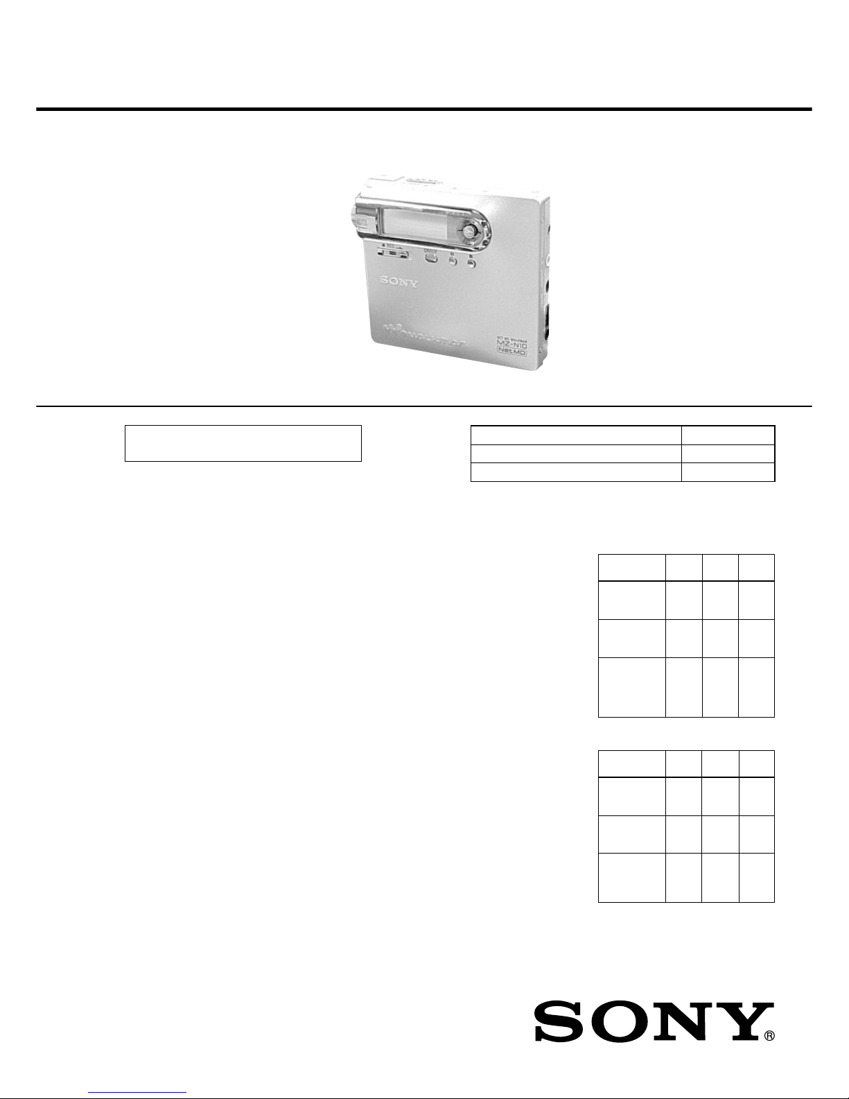
MZ-N10
Ver 1.2 2003. 02
US Model
Canadian Model
AEP Model
UK Model
E Model
Australian Model
Chinese Model
Tourist Model
PORTABLE MINIDISC RECORDER
9-874-284-03 Sony Corporation
2003B1600-1 Personal Audio Company
C 2003.02 Published by Sony Engineering Corporation
– Continued on next page –
US and foreign patents licensed from Dolby
Laboratories.
Model Name Using Similar Mechanism NEW
Mechanism Type MT-MZN10-181
Optical Pick-up Name ABX-1R
SPECIFICATIONS
Audio playing system
MiniDisc digital audio system
Laser diode properties
Material: GaAlAs
Wavelength: λ = 790 nm
Emission duration: continuous
Laser output: less than 44.6 µW
(This output is the value measured at a distance
of 200 mm from the lens surface on the optical
pick-up block with 7 mm aperture.)
Recording and playback time (when
using MDW-80)
Maximum 160 min. in monaural
Maximum 320 min. in LP4 stereo
Revolutions
350 rpm to 3,600 rpm (CLV)
Error correction
ACIRC (Advanced Cross Interleave Reed
Solomon Code)
Sampling frequency
44.1 kHz
Sampling rate converter
Input: 32 kHz/44.1 kHz/48 kHz
Coding
ATRAC (Adaptive TRansform Acoustic
Coding)
ATRAC3 — LP2/LP4
Modulation system
EFM (Eight to Fourteen Modulation)
Frequency response
20 to 20,000 Hz ± 3 dB
When recording
(Unit: approx.hours)(JEITA4))
Batteries SP
Stereo
LP2
Stereo
LP4
Stereo
Built-in
rechargeable
battery
5)
8.5 11 14
LR6 (SG)
Sony alkaline
dry battery
6)
7.5 10 11.5
Built-in
rechargeable
battery
5)
+ One LR6
(SG)
6)
15 20 26.5
When playing
(Unit: approx.hours)(JEITA)
Batteries SP
Stereo
LP2
Stereo
LP4
Stereo
Built-in
rechargeable
battery
17 20 24
LR6 (SG)
Sony alkaline
dry battery
27 32 36
Built-in
rechargeable
battery + One
LR6 (SG)
42 52 58
Battery operation time
3)
Inputs
1)
MIC: stereo mini-jack
(minimum input level 0.25 mV)
Line in: stereo mini-jack for analog input
(minimum input level 49 mV)
optical (digital) mini-jack for optical
(digital) input
Outputs
i/LINE OUT2): stereo mini-jack (dedicated
remote control jack)/194 mV (10 kΩ)
Maximum output (DC)
2)
Headphones:
2.0 mW + 2.0 mW (16 Ω) (European
models)
5 mW + 5 mW (16 Ω) (Other models)
Power requirements
Sony AC Power Adaptor connected at the DC
IN 6V jack:
120 V AC, 60 Hz (Models for USA, Canada,
Mexico and Taiwan)
230 - V AC, 50/60 Hz (Models for continental
Europe, Singapore and Thailand)
240 V AC, 50 Hz (Model for Australia)
220 V AC, 50 Hz (Model for China)
230 - V AC, 50 Hz (Models for U.K. and
Hong Kong)
100 - 240 V AC, 50/60 Hz (Other models)
The recorder:
Lithium-ion rechargeable battery (Built-in)
LIP-3WMB, 3.7 V, 340 mAh, Li-ion
LR6 (size AA) alkaline battery
USB cradle:
AC power adaptor DC 6V
SILVER MODEL
Page 2
2
MZ-N10
CAUTION
Use of controls or adjustments or performance of procedures
other than those specified herein may result in hazardous radiation exposure.
Notes on chip component replacement
•Never reuse a disconnected chip component.
• Notice that the minus side of a tantalum capacitor may be damaged by heat.
Flexible Circuit Board Repairing
•Keep the temperature of the soldering iron around 270 ˚C during repairing.
• Do not touch the soldering iron on the same conductor of the
circuit board (within 3 times).
• Be careful not to apply force on the conductor when soldering
or unsoldering.
UNLEADED SOLDER
Boards requiring use of unleaded solder are printed with the leadfree mark (LF) indicating the solder contains no lead.
(Caution: Some printed circuit boards may not come printed with
the lead free mark due to their particular size)
: LEAD FREE MARK
Unleaded solder has the following characteristics.
• Unleaded solder melts at a temperature about 40 ˚C higher than
ordinary solder.
Ordinary soldering irons can be used but the iron tip has to be
applied to the solder joint for a slightly longer time.
Soldering irons using a temperature regulator should be set to
about 350 ˚C .
Caution: The printed pattern (copper foil) may peel away if the
heated tip is applied for too long, so be careful!
• Strong viscosity
Unleaded solder is more viscous (sticky, less prone to flow) than
ordinary solder so use caution not to let solder bridges occur
such as on IC pins, etc.
• Usable with ordinary solder
It is best to use only unleaded solder but unleaded solder may
also be added to ordinary solder.
On power sources
• Use house current, nikel metal hydride rechargeable battery,
LR6 (SG) battery, or car battery.
• For use in your house: For the supplied battery charging
stand, use the AC power adaptor supplied with this recorder.
Do not use any other AC power adaptor since it may cause
the recorder to malfunction
Polarity of the
plug
SAFETY-RELATED COMPONENT WARNING!!
COMPONENTS IDENTIFIED BY MARK 0 OR DOTTED
LINE WITH MARK 0 ON THE SCHEMATIC DIAGRAMS
AND IN THE PARTS LIST ARE CRITICAL TO SAFE
OPERATION. REPLACE THESE COMPONENTS WITH
SONY PARTS WHOSE PART NUMBERS APPEAR AS
SHOWN IN THIS MANUAL OR IN SUPPLEMENTS PUBLISHED BY SONY.
Optical cable (1)
CD-ROM (SonicStage Ver. 1.5) (1)*
Carrying pouch/carrying case with a belt clip (except USA model) (1)
Recordable MD (USA and Canada models only) (1)
∗Do not play a CD-ROM on an audio CD player.
Headphones/earphones with a remote control (1)
Dimensions
Approx. 78.5 × 73.3 × 13.8 mm (w/h/d)
(3
1
/8× 3 ×9/16 in.) (excluding projecting parts
and controls)
Mass
Approx. 84 g (3 oz) (including the built-in
rechargeable battery)
1)
The LINE IN (OPT) jack is used to connect
either a digital (optical) cable or a line
(analog) cable.
2)
The i/LINE OUT jack connects either
headphones/earphones or a line cable.
3)
Measured in accordance with JEITA.
US and foreign patents licensed from Dolby
Laboratories.
Design and specifications are subject to change
without notice.
4)
Measured in accordance with the JEITA
(Japan Electronics and Information
Technology Industries Association) standard.
5)
When using a 100% fully charged
built-in
lithiun-ion
rechargeable battery.
6)
When using a Sony LR6 (SG) “STAMINA”
alkaline dry battery (produced in Japan).
Supplied accessories
AC power adaptor (1)
USB cradle (1)
Dedicated USB cable (1)
Dry battery case (1)
• SonicStage, OpenMG and the OpenMG
logo, MagicGate, Memory Stick and the
MagicGate Memory Stick logo,
Memory Stick and the Memory Stick
logo, Net MD and the Net MD logo are
trademarks of Sony Corporation.
• Microsoft, Windows, Windows NT and
Windows Media are trademarks or
registered trademarks of Microsoft
Corporation in the United States and /or
other countries.
• IBM and PC/AT are registered
trademarks of International Business
Machines Corporation.
• Macintosh is a trademark of Apple
Computer, Inc. in the United States and/
or other countries.
• MMX and Pentium are trademarks or
registered trademarks of Intel
Corporation.
• All other trademarks and registered
trademarks are trademarks or registered
trademarks of their respective holders.
• ™ and ® marks are omitted in this
manual.
Ver 1.2 2003.02
ATTENTION AU COMPOSANT AYANT RAPPORT
À LA SÉCURITÉ!
LES COMPOSANTS IDENTIFÉS PAR UNE MARQUE 0 SUR LES
DIAGRAMMES SCHÉMATIQUES ET LA LISTE DES PIÈCES
SONT CRITIQUES POUR LA SÉCURITÉ DE FONCTIONNEMENT.
NE REMPLACER CES COMPOSANTS QUE PAR DES PIÈSES
SONY DONT LES NUMÉROS SONT DONNÉS DANS CE MANUEL
OU DANS LES SUPPÉMENTS PUBLIÉS PAR SONY.
Page 3

3
MZ-N10
TABLE OF CONTENTS
1. SERVICING NOTES ............................................... 4
2. GENERAL ................................................................... 5
3. DISASSEMBLY ......................................................... 6
3-1. Bottom Panel Section, Jog Dial Section......................... 7
3-2. Upper Panel Section........................................................ 7
3-3. MAIN Board Section ...................................................... 8
3-4. MD Mechanism Deck (MT-MZN10-181),
Set Chassis ...................................................................... 8
3-5. Gear (SA), Gear (SB)...................................................... 9
3-6. OP Service Assy (ABX-1R) ........................................... 9
3-7. DC Motor SSM21A (Sled) (M602),
DC Motor SSM18D (Spindle) (M601),
DC Motor Unit (Over Write Head Up/Down)
(M603) ............................................................................. 10
3-8. Holder Assy ..................................................................... 10
4. TEST MODE .............................................................. 11
5. ELECTRICAL ADJUSTMENTS ......................... 17
6. DIAGRAMS
6-1. Block Diagram ................................................................ 37
6-2. Note for Printed Wiring Board and
Schematic Diagrams ....................................................... 38
6-3. Printed Wiring Board
– MAIN Board (Side A) – ......................................... 39
– MAIN Board (Side B) – ......................................... 40
6-4. Schematic Diagrams
– MAIN Board (1/4) – ............................................... 41
– MAIN Board (2/4) – ............................................... 42
– MAIN Board (3/4) – ............................................... 43
– MAIN Board (4/4) – ............................................... 44
6-5. IC Pin Function Description ........................................... 49
7. EXPLODED VIEWS
7-1. Upper Panel Section........................................................ 55
7-2. Bottom Panel Section...................................................... 56
7-3. Chassis Section ............................................................... 57
7-4. MD Mechanism Deck Section (MT-MZN10-181) ........ 58
8. ELECTRICAL PARTS LIST ............................... 59
Page 4
4
MZ-N10
NOTES ON HANDLING THE OPTICAL PICK-UP
BLOCK OR BASE UNIT
The laser diode in the optical pick-up block may suffer electrostatic break-down because of the potential difference generated
by the charged electrostatic load, etc. on clothing and the human
body.
During repair, pay attention to electrostatic break-down and also
use the procedure in the printed matter which is included in the
repair parts.
The flexible board is easily damaged and should be handled with
care.
NOTES ON LASER DIODE EMISSION CHECK
Never look into the laser diode emission from right above when
checking it for adjustment. It is feared that you will lose your sight.
NOTES ON HANDLING THE OPTICAL PICK-UP BLOCK
(ABX-1R)
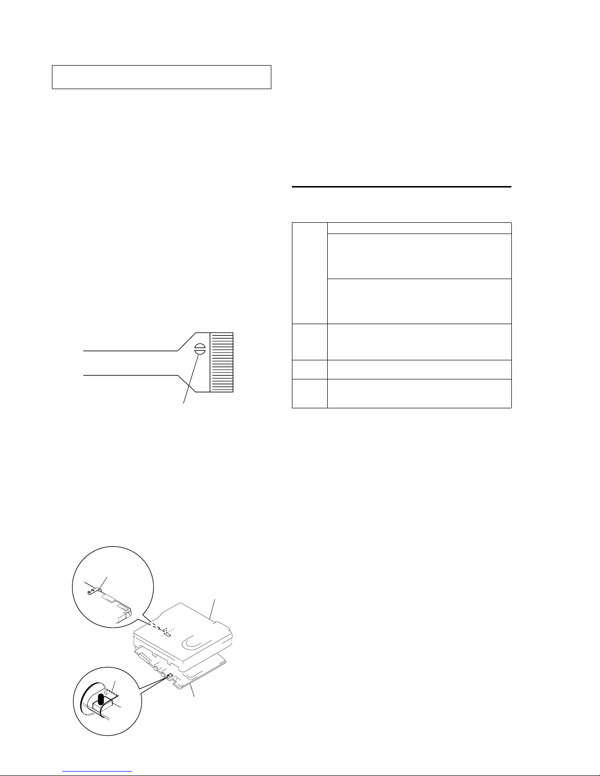
The laser diode in the optical pick-up block may suffer electrostatic break-down easily. When handling it, perform soldering
bridge to the laser-tap on the flexible board. Also perform measures against electrostatic break-down sufficiently before the operation. The flexible board is easily damaged and should be handled
with care.
SECTION 1
SERVICING NOTES
• In performing the repair with the power supplied to the set, removing the MAIN board causes the set to be disabled.
In such a case, fix a convex part of the open/close detect switch
(S803 on MAIN board) with a tape in advance.
• Handle the FLEXIBLE board (over write head) with care, as it
has been soldered directly to the MAIN board.
In repairing the component side of MAIN board, connect the
FLEXIBLE board (over write head) and the MAIN board with
the lead wires in advance.
laser-tap
OPTICAL PICK-UP FLEXIBLE BOAR
D
upper panel assy
MAIN board
S803
tape
FLEXIBLE board
(over write head)
•Replacement of SN761058ZQL (IC501), CDX2678-202GA
(IC801) used in this set requires a special tool
•The shipment data will be cleared when the NV is reset. Therefore, change the NV adjusted values following the Change of
NV Adjusted Values immediately after the NV was reset. (See
page 17)
•This set requires the patch data in the nonvolatile memory
(IC851) to be rewritten using the application, when the MAIN
board was replaced. (See page 28)
System requirements
The following hardware and software are required in order to use the
SonicStage software for the Net MD.
This software is not supported by the following
environments:
• Macintosh
• Windows XP versions other than Home Edition or Professional
• Windows 2000 versions other than Professional
• Windows 98 versions other than Second Edition
• Windows NT
• Windows 95
• Personally constructed PCs or operating systems
• An environment that is an upgrade of the original manufacturer-installed
• Multi-boot environment
• Multi-monitor environment
Notes
• We do not ensure trouble-free operation on all computers that satisfy the
• We do not ensure trouble-free operation of the system suspend, sleep, or
hibernation function on all computers.
Computer IBM PC/AT or Compatible
•CPU: Pentium II 400 MHz or higher
(Pentium III 450 MHz or higher is recommended.)
•Hard disk drive space
1)
: 120 MB or more
•
1)
Others
•CD-ROM drive (capable of digital playback by WDM)
•Sound Board
•
Operating
System
Factory installed:
Windows XP Home Edition/Windows XP Professional/
Windows Millennium Edition/Windows 2000 Professional/
Windows 98 Second Edition
Display High Color (16bit) or greater, 800 × 480 dots or more
Others • Internet access: for Web registration and EMD services
•
Note on hard disk drive space
120 MB or more free space on the hard disk drive is required. If your
computer does not have enough space, the software will not be properly
installed. The required free space differs according to the version of
your Windows OS, or the amount of audio files that you handle.
USB port (supports USB 2.0 Full Speed
(previously USB 1.1))
(800 × 600 dots or more is recommended)
Windows Media Player (version 7.0 or higher) installed for
playing WMA files
RAM: 64 MB or higher
(128 MB or higher is recommended)
operating system
system requirements.
Page 5
5
MZ-N10
SECTION 2
GENERAL
This section is extracted from
instruction manual.
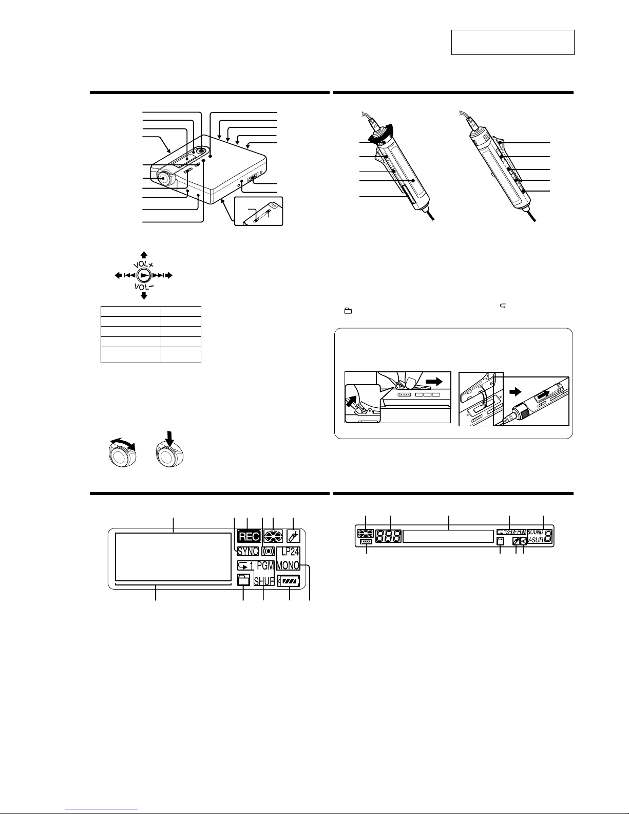
Looking at controls
The recorder
A 5-way control key
B Charge lamp
C Display window
D OPEN switch
E GROUP button
G zREC (record) switch
H T MARK button
I END SEARCH button
J X button
K x button
L Handstrap hole
Use the hole to attach your own strap.
M LINE IN (OPT) jack
N MIC (PLUG IN POWER) jack
There is a tactile dot beside the MIC
(PLUG IN POWER) jack.
O i (headphones/earphones)/LINE
OUT jack
P USB cradle connecting jack
1
2
3
6
5
4
7
qj
qh
qd
qs
qa
qf
qg
9
q;
8
qk
ql
Operation Function
Press N
1)
1)
The N and VOL + button has a tactile
dot.
play
Press towards . rewind
Press towards > fast forward
Press towards
VOL+, –.
volume
S BUILT-IN BATTERY switch
Slide the switch to ON when using
the recorder for the first time, and
keep it ON thereafter (it is factory
set to OFF).
The display window of the recorder
A Character information display
Displays the disc and track names,
date, error messages, track numbers,
etc.
B SYNC (synchro-recording) indication
C REC indication
Lights up while recording. When
flashing, the recorder is in record
standby mode.
D Melody timer indication
E Disc indication
Shows that the disc is rotating for
recording or playing.
F Bookmark indication
Lights up when playing a bookmarked
track.
G Level meter
H Group indication
I Play mode indication
Shows the play mode (shuffle play,
program play, repeat play, etc.) of the
MD.
J Battery indication
Shows the approximate remaining
battery charge. If the built-in
rechargeable battery is weak, the
indication becomes empty and starts
flashing. The recorder will first draw
power from the built-in rechargeable
battery, even if a dry battery is
inserted in the dry battery case. It
switches automatically to the dry
battery when the built-in rechargeable
battery becomes drained. While the
recorder is using the power from the
dry battery, the frame around the
indication will begin slowly flashing.
K LP2, LP4, MONO (monaural)
indication
1 42 5 6
qa9 q;87
3
The headphones/earphones with a remote control
A Vo lume control (VOL+, –)
Turn to adjust the volume.
B x (stop) button
C Jog lever (NX/ENT, ., >)
NX/ENT (to press): play, pause,
enter
.(to slide towards): REW
> (to slide towards): FF
D Display window
E (group) +, –
F Clip
G HOLD switch
Slide the switch in the direction of the
arrow (a yellow mark appears) to
disable the buttons on the remote
control. To prevent the buttons from
being accidentally operated when you
carry the recorder, use this function.
H DISPLAY button
I P MODE/ button
J SOUND button
F
G
H
I
J
B
C
D
E
A
The display window of the remote control
A Disc indication
B Track number display
C Character information display
D Play mode indication
E SOUND indication
F Battery level indication
G Group indication
H Bookmark indication
I Melody timer indication
1
2
Using the clip for the remote control
The clip can be removed and reattached in the opposite direction.
Removing the clip
Attaching the clip in the opposite
direction
F
GHI
BADEC
Q A terminal for attaching dry battery
case
R HOLD switch
Slide the switch in the direction of the
arrow to disable the buttons on the
recorder. To prevent the buttons from
being accidentally operated when you
carry the recorder, use this function.
F Jog dial (MENU/ENTER)
Turn to select
Push to enter
Page 6
6
MZ-N10
SECTION 3
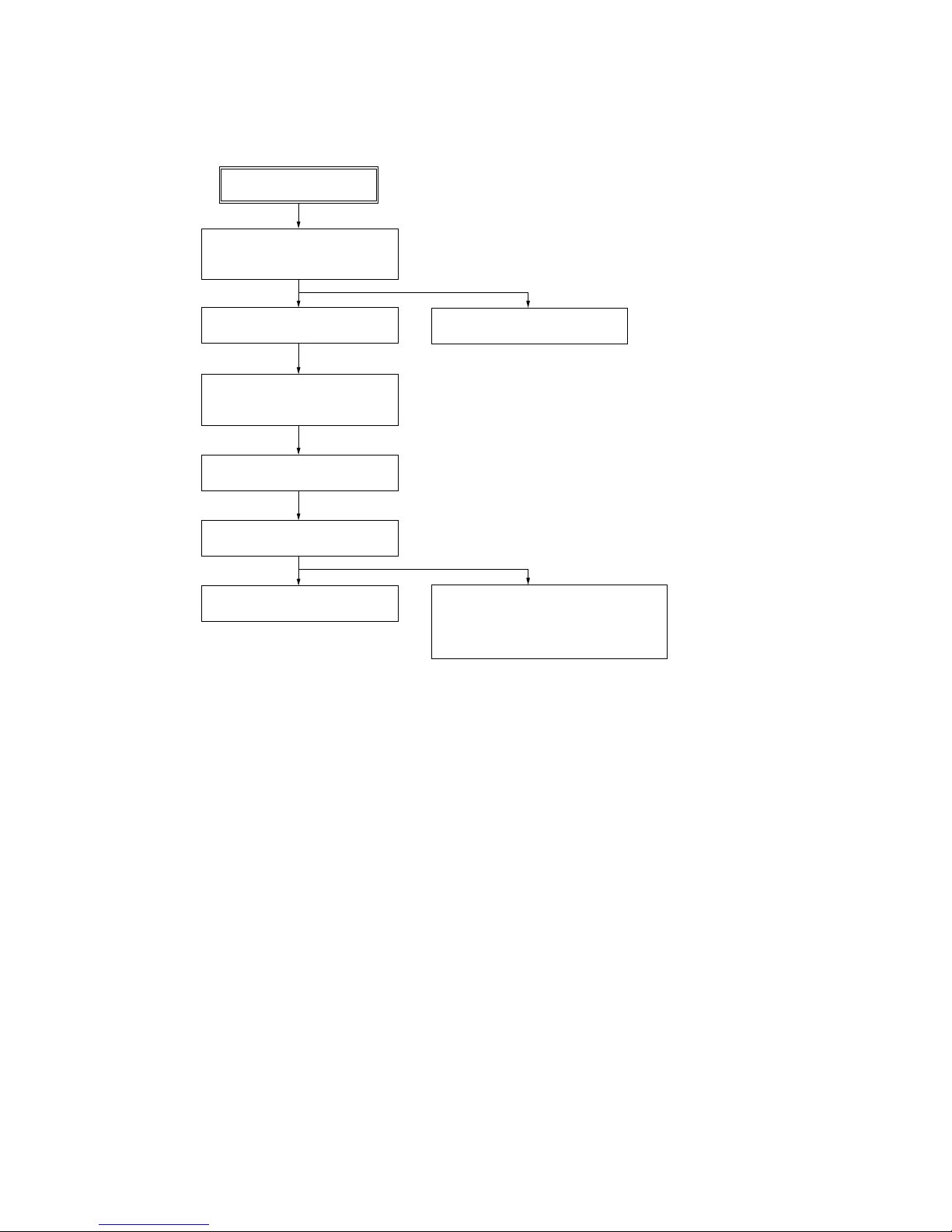
DISASSEMBLY
BOTTOM PANEL SECTION,
JOG DIAL SECTION
UPPER PANEL SECTION
SET
MAIN BOARD SECTION
GEAR (SA), GEAR (SB)
OP SERVICE ASSY (ABX-1R)
DC MOTOR SSM21A (SLED) (M602),
DC MOTOR SSM18D (SPINDLE) (M601),
DC MOTOR UNIT (OVER WRITE HEAD
UP/DOWN) (M603)
HOLDER ASSY
MD MECHANISM DECK
( MT-MZN10-181),
SET CHASSIS
• The equipment can be removed using the following procedure.
Page 7
7
MZ-N10
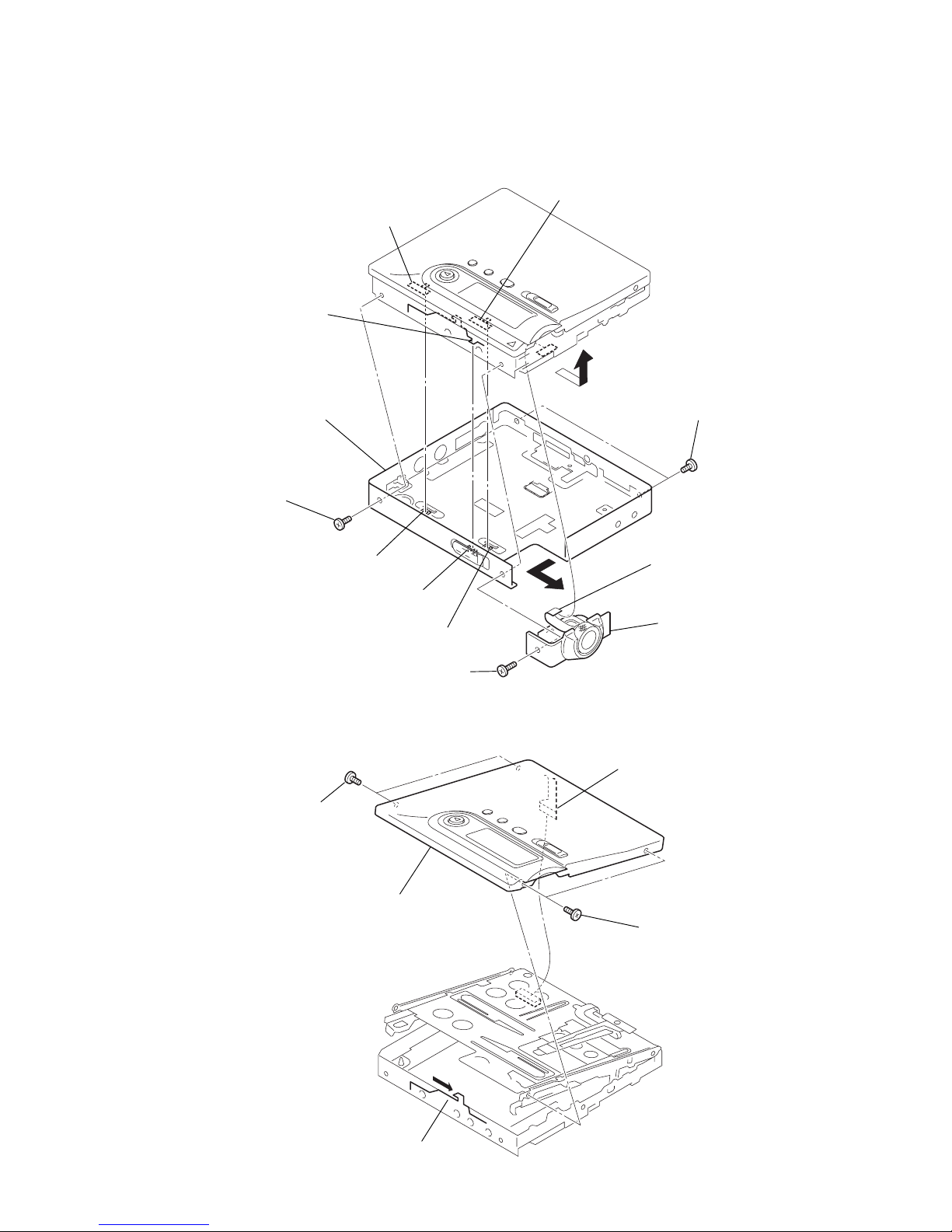
3-1. Bottom Panel Section, Jog Dial Section
S802
S951
5
4
3
two screws
(M1.4)
1
screw (M1.4)
2
screw (M1.4)
knob (HOLD)
knob (OPEN)
knob (BATT)
6
bottom panel assy
Notes: On installation, adjust the position of both switch (S802) and knob (hold).
@@@
Adjust the position of both switch (S951) and knob (batt).
@@@
Adjust the position of both the convex part of an open lever and knob (open).
The convex part of an open lever
7
flexible board (CN891
)
8
jog dial assy
3-2. Upper Panel Section
2
Slide the open lever in the direction of the arrow,
and open the upper panel section.
3
two screws
(M1.4)
4
two screws
(M1.4)
5
upper panel assy
1
flexible board (CN871
)
Page 8
8
MZ-N10
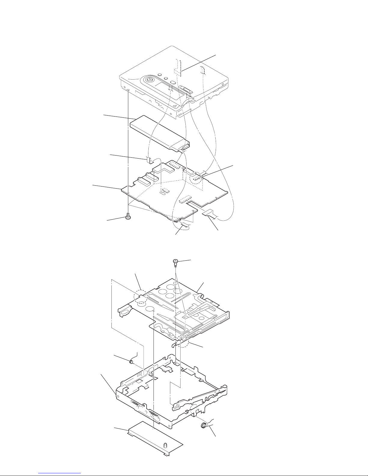
3-3. MAIN Board Section
3-4. MD Mechanism Deck (MT-MZN10-181), Set Chassis
1
five toothed lock screws
(M1.4)
3
flexible board (CN871)
6
flexible board (CN951)
5
flexible board (CN501)
2
flexible board (CN701)
7
lithium ion storage battery
8
MAIN board
4
Remove two solders of th
e
main board.
1
two step screws
(MD)
3
boss
6
torsion spring (pop-R
)
7
torsion spring (pop-L)
2
boss
4
MD mechanism deck
(MT-MZN10-181)
8
set chassis assy
5
battery case
Page 9
9
MZ-N10
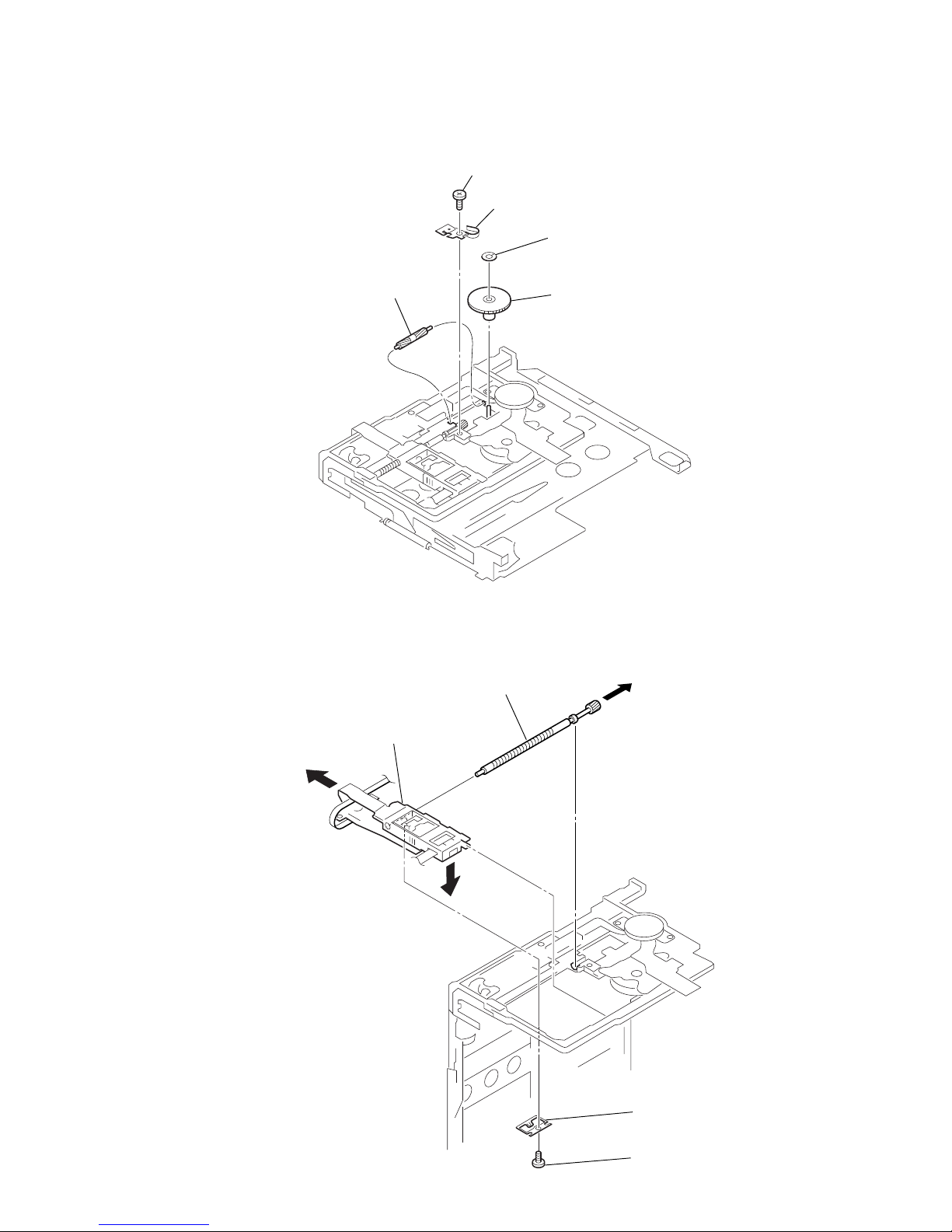
3-5. Gear (SA), Gear (SB)
3-6. OP Service Assy (ABX-1R)
1
tapping screw
2
spring
4
gear (SA)
3
washer (0.8-2.5)
5
gear (SB)
5
OP service assy (ABX-1R)
3
Pull off lead screw.
1
precision pan screw (M1.4)(EG
)
2
rack spring
4
Opening the over write head
toward the direction A, remove the OP service assy
(ABX-1R) toward the direction B.
A
B
Note: Do not the entire assy forcibly,
when opening the over write head.
Page 10
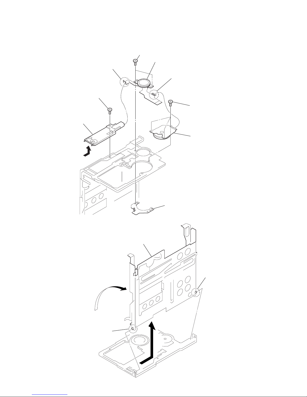
10
MZ-N10
3-7. DC Motor SSM21A (Sled) (M602), DC Motor SSM18D (Spindle) (M601),
DC Motor Unit (Over Write Head Up/Down) (M603)
3
two screws
(M1.4)
8
screw
6
three screws
5
motor base assy
9
DC motor unit (over write head up/down)
(M603)
7
DC motor SSM18D (spindle) (M601)
4
DC motor SSM21A (sled) (M602)
2
Remove two solders of the
flexible board.
1
Remove four solders of the
flexible board.
A
2
bos
s
1
boss
3
Open the holder assy.
4
Remove the holder assy in the direction of the arrow A.
3-8. Holder Assy
Page 11
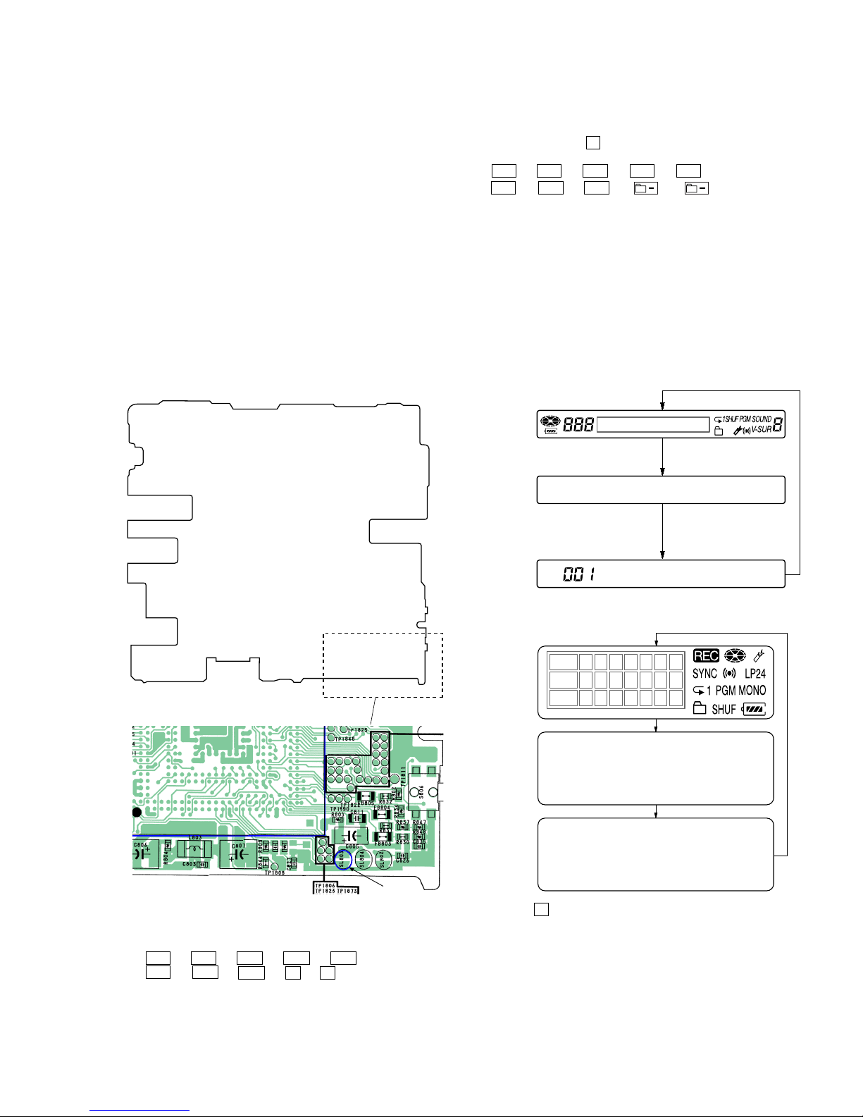
11
MZ-N10
3 In case of setting the test mode by keys on the set and
remote commander:
In the normal mode, turn on the [HOLD] switch on the set.
While pressing the x key on the set, press the keys on the
remote commander with the following order:
> t > t . t . t > t
. t > t . t t
Note: If electrical adjustment (CD and MO overall adjustment) has not
been finished completely, “ERROR” is displayed on LCDs of the
set and the remote commander.
Operation in Setting the Test Mode
•When the test mode becomes active, first the display check mode
is selected.
• Other mode can be selected from the display check mode.
•When the test mode is set, the LCD repeats the following display.
Remote commander LCD display
Set LCD display
• When the X key is pressed and hold down, the display at that
time is held so that display can be checked.
Releasing the Test Mode
For test mode set with the method 1:
Turn off the power and open the solder bridge on SL803 (TEST)
on the MAIN board.
Note: Remove the solders completely. Remaining could be shorted with
the chassis, etc.
For test mode set with the method 2 or 3:
Turn off the power.
2 In case of setting the test mode only by keys on the set:
In the normal mode, turn on the [HOLD] switch. While pressing the [GROUP] key press the following order:
> t > t . t . t > t
. t > t . t X t X
SECTION 4
TEST MODE
Outline
•This set provides the Overall adjustment mode that allows CD
and MO discs to be automatically adjusted when in the test mode.
In this overall adjustment mode, the disc is discriminate between
CD and MO, and each adjustment is automatically executed in
order. If a fault is found, the system displays its location. Also,
the manual mode allows each individual adjustment to be automatically adjusted.
• Operation in the test mode is performed with the set. A key
having no particular description in the text, indicates a set key.
•For the LCD display, the LCD on the remote commander is
shown, but the contents of LCD display on the set are same.
(Both displays may be displayed.)
Setting Method of Test Mode
There are three different methods to set the test mode:
1 Short SL803 (TEST) on the MAIN board with a solder bridge
(connect pin <zx. of IC801 to the ground) and turn on the power.
V1.100
Microcomputer
version
display
All off
All lit
Ver 1.100
001
Microcomputer
version
display
All off
All lit
IC801
1-686-347-
TP1829
C815
R838
– MAIN Board (Side B) –
Page 12
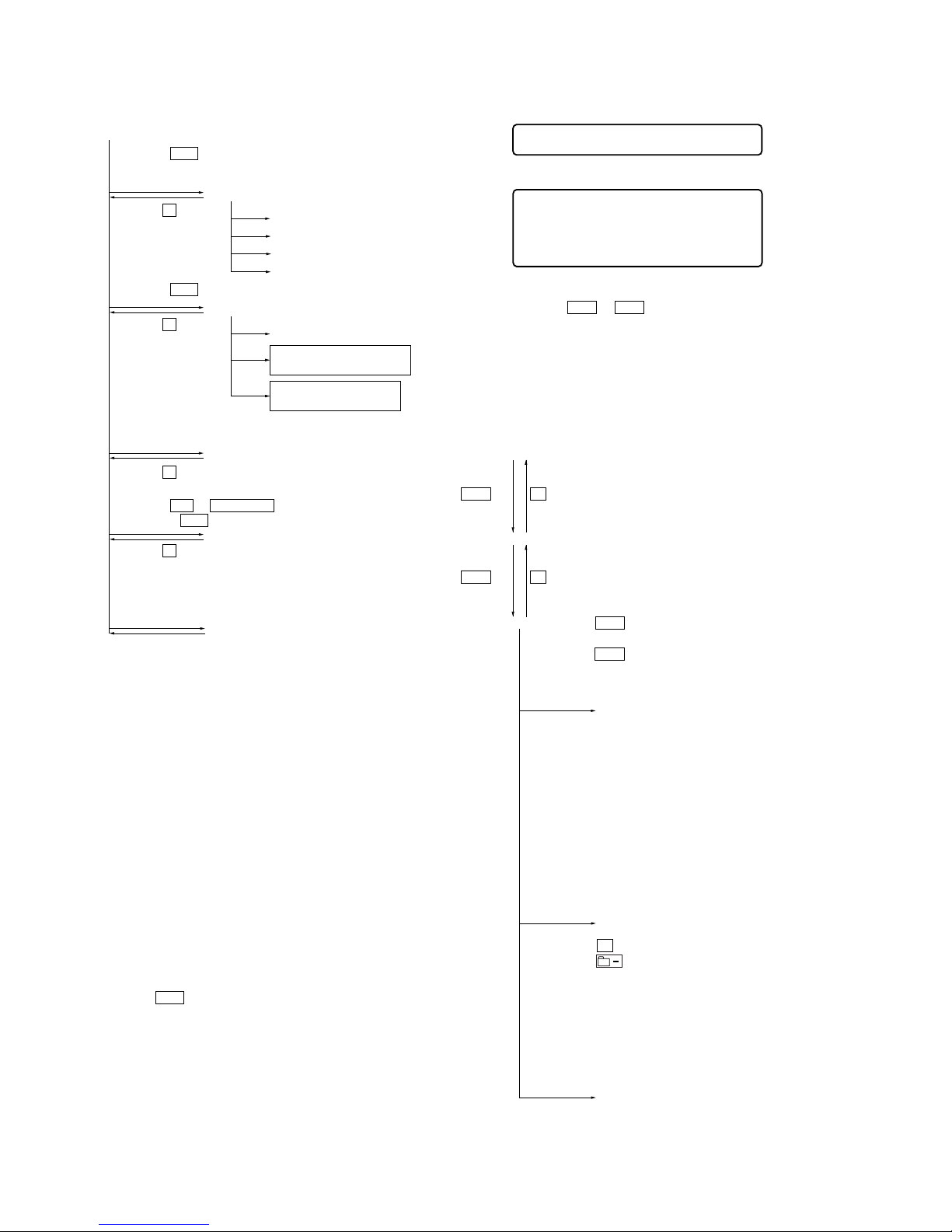
12
MZ-N10
Configuration of Test Mode
Manual Mode
Mode to adjust or check the operation of the set by function.
Normally, the adjustment in this mode is not executed.
However, the Manual mode is used to clear the memory, power
supply adjustment, and laser power check before performing
automatic adjustments in the Overall Adjustment mode.
The manual mode consists of a major item, a medium item and a
minor item.
The manual mode is divided into four groups of major items.
SERVO : item number 000 - 500, 800 AUDIO : item number 600 POWER : item number 700 OP : item number 900 A medium item divides a major item and is used to select functions.
In a minor item, adjustments or operation checks are performed.
•Transition method in manual mode
1. Set the test mode (see page 11).
2. Press the > key, [VOL +] key or [VOL +] key on the remote commander activates the manual mode where the LCD
display as shown below.
Press the x key
[Manual Mode]
[Servo Adjustment]
[Audio Adjustment]
[Power Supply Adjustment]
[OP Alignment Adjustment]
[Overall Adjustment Mode]
[Sound Skip Check Result Display Mode]
[Key Check Mode]
[Test Mode $Display Check Mode%]
Press the x key
Press the x key
Press the x key
Press the . or [VOL --] key
Press the N or z
REC .
key,
or press the > key on the remote commander
Press the > or [VOL +] key,
or press the
[VOL +] key on the remote commander
[Electrical Offset Adjustment]
Power Supply Adjustment
Auto Item Feed
CD Overall Adjustment/
MO Overall Adjustment
[Self-Diagnosis Result Display Mode]
Turn the jog dial (down),
or press the [DISPLAY] key on the remote commander
Press the
[T MARK] key, or press the [DISPLAY] key
on the remote commander for several
seconds (about 3 seconds)
The key check quits, or open the upper panel
Manual
000
Manual
000
Remote commander LCD display
Set LCD display
3. During each test, the optical pick-up moves outward or inward while the > or . key is pressed for several seconds respectively.
4. Each test item is assigned with a 3-digit item number;
100th place is a major item, 10th place is a medium item, and
unit place is a minor item.
The values adjusted in the test mode are written to the nonvolatile memory (for the items where adjustment was made).
x
key
[VOL +]
key: 100th place of item
number increase.
[VOL --]
key: 100th place of item
number decrease.
[Major item switching]
[VOL +]
key: 10th place of item
number increase.
[VOL --]
key: 10th place of item
number decrease.
[VOL +]
key: Increases the adjusted
value of the 1st digit
[VOL --]
key: Decreases the adjusted
value of the 1st digit
[Medium item switching]
x
key
>
key
>
key
[Minor item switching]
[Adjusted value variation]
X
key or
key of the remote commander:
When adjusted value is
changed:
Adjusted value is written.
When adjusted value is
not changed:
That item is adjusted
automatically.
[Adjusted value write]
[RAM monitor]
>
key: Unit place of item number
increase.
.
key: Unit place of item number
decrease.
[P MODE]
key of
the remote commander:
Increase the adjusted value
of the 2nd digit
[SOUND]
key of the remote commander:
Decrease the adjusted value
of the 2nd digit
[T MARK]
key or
[SOUND]
key of the remote commander
for several seconds
Page 13
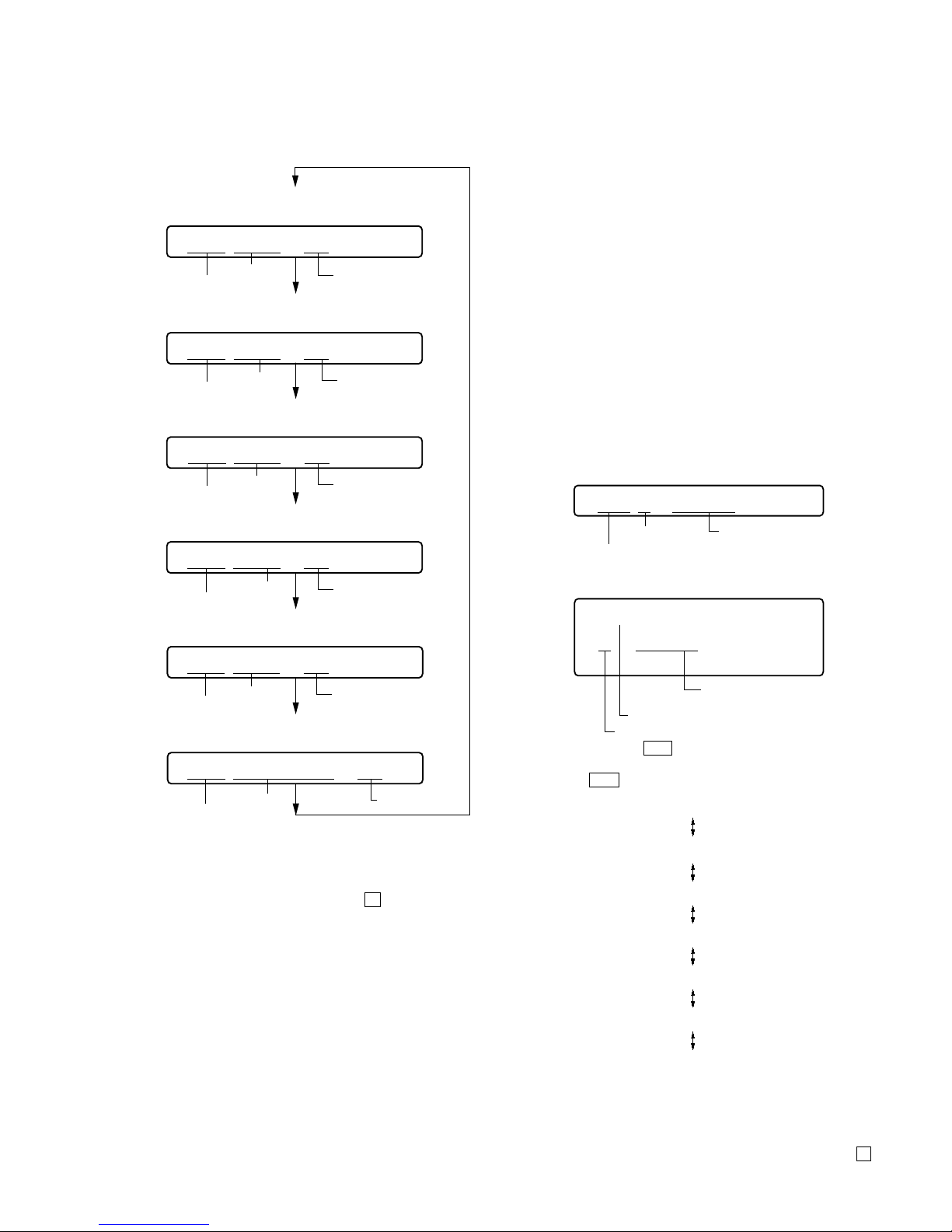
13
MZ-N10
Self-Diagnosis Result Display Mode
This set uses the self-diagnostic function system in which if an
error occurred during the recording or playing, the mechanism
control block and the power supply control block in the
microcomputer detect it and record its cause as history in the
nonvolatile memory.
By checking this history in the test mode, you can analyze a fault
and determine its location.
Total recording time is recorded as a guideline of how long the
optical pick-up has been used, and by comparing it with the total
recording time at the time when an error occurred in the selfdiagnosis result display mode, you can determine when the error
occurred.
Clear both self-diagnosis history data and total recording time, if
the optical pick-up was replaced.
• Self-diagnosis result display mode setting method
1. Set the test mode (see page 11).
2. In the display check mode, turning the jog dial (down) or pressing the [DISPLAY] key on the remote commander activates
the self-diagnosis result display mode where the LCD display
as shown below.
3. Then, each time the
> key is pressed, LCD display descends
by one as shown below. Also, the LCD display ascends by one
when the . key is pressed.
If the jog dial (down) is turned or the [DISPLAY] key on remote
commander is pressed with this display, the LCD switches to the
simple display mode.
4. Quit the self-diagnosis result display mode, and press the x
key to return to the test mode (display check mode).
5. The display changes a shown below each time the jog
dial (down) is turned or the [DISPLAY] key on the remote
commander is pressed.
However in the power mode (item number 700’s), only the
item is displayed.
6. Quit the manual mode, and press the
x key to return to the
test mode (display check mode).
Overall Adjustment Mode
Mode to adjust the servo automatically in all items.
Normally, automatic adjustment is executed in this mode at the
repair.
For further information, refer to “SECTION 5 ELECTRICAL
ADJUSTMENTS” (see page 17).
item number
address
adjusted value
item number
jitter value
adjusted value
item number
block error
value
adjusted value
item number
ADIP error
value
Focus drive
value
adjusted value
item number
adjusted value
item number
item title
adjusted value
• Address & Adjusted Value Display
Remote commander LCD display
• Jitter Value & Adjusted Value Display
Remote commander LCD display
C68S01
011
• Block Error Value & Adjusted Value Display
Remote commander LCD display
• ADIP Error Value & Adjusted Value Display
Remote commander LCD display
• Focus Drive Value & Adjusted Value Display
Remote commander LCD display
• Item Title Display
Remote commander LCD display
063B01
011
059A01
011
015F01
011
OFFJ01
011
LrefPw 01
011
Remote commander LCD display
Set LCD display
history code
history code
Total recording time
when error occurred
Total recording time
when error occurred
error display code
error display code
1 0000
0XX
1 0000
0XX
0XX 1 ****
0XX N ****
0XX N1****
0XX N2****
0XX R_****
1
1
XX
: Error code
****
: Total recording time
Page 14
14
MZ-N10
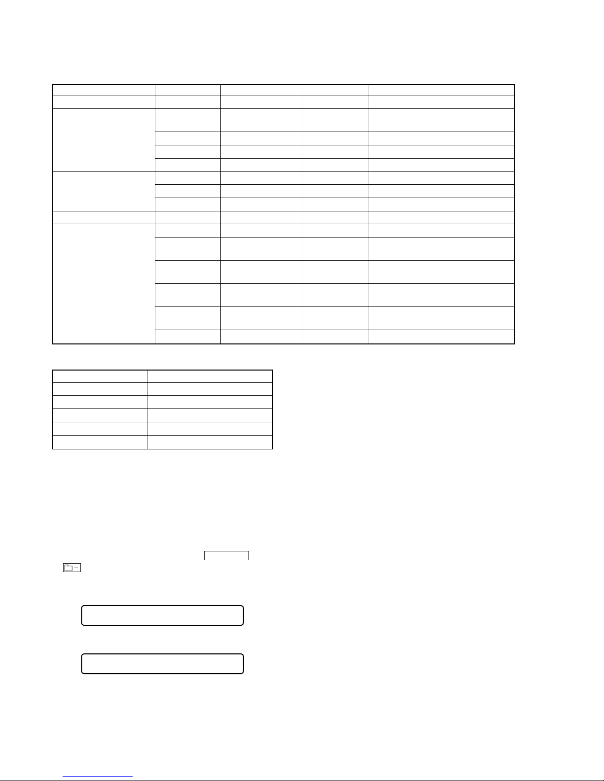
• Description of indication history
History code number Description
1The first error
N The last error
N1 One error before the last.
N2 Two errors before the last.
R_ Total recording time
Reset the Error Display Code
After servicing, reset the error display code.
• Setting method of reset the error display code
1. Set the test mode (see page 11).
2. Turning the jog dial (down) or pressing the [DISPLAY] key on
the remote commander activates the self-diagnosis result display mode.
3. To reset the error display code, press the zREC. key or
key on the remote commander (twice) when the code is
displayed (except “R_****”).
(All the data on the 1, N, N1, and N2 will be reset)
• Description of error indication codes
Problem Indication code Meaning of code Simple display Description
No error 00 No error --- No error
01
Illegal access target
Adrs Attempt to access an abnormal address
address was specified
Servo system error 02 High temperature Temp High temperature detected
03 Focus error Fcus Disordered focus or can not read an address
04 Spindle error Spdl Abnormal rotation of disc
11 TOC error TOC Faulty TOC contents
TOC error 12 Data reading error Data Data could not be read at SYNC
13 TOC address error Tadr TOC address data error
Power supply system error 22 Low battery LBat Momentary interruption detected
31 Offset error Ofst Offset error
32
Focus error ABCD
ABCD Focus error ABCD offset error
offset error
33
Tracking error
TE Tracking error Offset error
Offset system error Offset error
34
X1 tracking error
X1TE X1 tracking error Offset error
Offset error
35
MD DATA 2
MD2 MD DATA 2 disc error
Disc error
36 Mirror error Mirr Mirror decision retry over
ClrOK?
000
ErrCLR
000
Remote commander LCD display
(Key pressing at the first time)
Remote commander LCD display
(Key pressing at the second time)
Page 15
15
MZ-N10
Key and Jog Check Mode
This set can check if the set and remote commander function normally.
• Setting method of key check mode
1. Set the test mode (see page 11).
2. Pressing the [T MARK] key or [DISPLAY] key on the remote
commander for several seconds (about 3 seconds) activates the
key check mode. (At the last two digits, AD value of remote commander key line is displayed in hexadecimal)
3. When each key on the set and on remote commander is pressed,
its name is displayed on the remote commander LCD. (The
operated position is displayed for 4 seconds after the slide
switch is operated. If any other key is pressed during this display, the remote commander LCD switches to its name display)
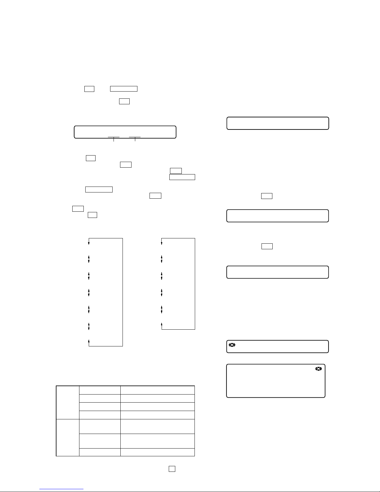
Example1: When the > key on the set is pressed:
Example2: When the
> key on the remote commander is
pressed:
4. When all the keys on the set and on the remote commander are
considered as OK, the following displays are shown for 4 seconds.
Example1: When the keys on the set are considered as OK:
Sound Skip Check Result Display Mode
This set can display the count of errors that occurred during the
recording/playing for checking.
• Setting method of sound skip check result display
mode
1. Set the test mode (see page 11).
2. Press the N key or zREC. key, and the playing or re-
cording sound skip check result display mode becomes active
respectively and press the > key on the remote commander,
and then the playing sound skip check result display mode
becomes active where the LCD displays the following.
3.
When theNkey is pressed, total error count is displayed on
the LCD, and each time the
>
key is pressed, the display item
moves down by one as shown below. Also, if the
.
key is
pressed, the display item moves up by one, then if the zREC.
key is pressed, the display in the record mode appears.
When the zREC. key is pressed, total error count is displayed on the LCD, and each time the > key is pressed,
the display item moves down by one as shown below. Also, if
the . key is pressed, the display item moves up by one,
then if the N key is pressed, the display in the play mode
appears.
• Cause of sound skip error
Cause of error Description of error
EIB Sound error correction error
Play
Stat Decoder status error
Adrs Address access error
BEmp Buffer is empty
BOvr
Buffer is full, and sounds were
dumped
Record
Bful
Buffer capacity becomes less,
and forcible writing occurred
Rtry Retry times over
4. To quit the sound skip check result display mode and to return
to the test mode (display check mode), press the x key.
Remote commander LCD display
Total count of play
system errors (hex.)
Total count of record
system errors (hex.)
P**R**
000
000 P**R**
000 EIB **
000 Stat**
000 Adrs**
000 BEmp**
000 ######
000 P**R**
000 BOvr**
000 Bful**
000 Rtry**
000 ######
P**R**
: Total play/record errors (hex.)
**
: Counter of sound skip check each item (hex.)
######
: 6-digit address where sound was skipped last (hex.)
Playing sound skip
result display
Recording sound skip
result display
Remote commander LCD display
**
: AD value of the remote commander key
(hexadecimal 00 to FF)
**
000
Remote commander LCD display
**
: AD value of the remote commander key
(hexadecimal 00 to FF)
FF **
000
Remote commander LCD display
**
: AD value of the remote commander key
(hexadecimal 00 to FF)
rFF **
000
Remote commander LCD display
Set LCD display
**
: AD value of the remote commander key
(hexadecimal 00 to FF)
SET OK **
888
SET OK **
888
Page 16
16
MZ-N10
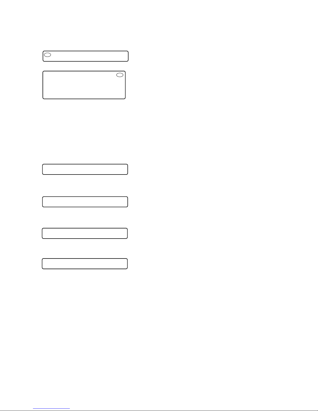
Example2: When the keys on the remote commander are con-
sidered as OK:
5. When all keys were checked or if the upper panel is opened,
the key check mode quits and the test mode (display check
mode) comes back.
• Jog check mode
Jog check mode is available during the key check mode.
1. Turn the jog dial downwards one click.
2. Turn the jog dial downwards three more clicks.
3. Turn the jog dial upwards one click.
4. Turn the jog dial upwards three more clicks.
Remote commander LCD display
Set LCD display
**
: AD value of the remote commander key
(hexadecimal 00 to FF)
RMC OK **
888
RMC OK **
888
Remote commander LCD display
JOG+ 1 **
000
Remote commander LCD display
JOG+OK **
000
Remote commander LCD display
JOG- 1 **
000
Remote commander LCD display
JOG-OK **
000
Page 17
17
MZ-N10
SECTION 5
ELECTRICAL ADJUSTMENTS
Outline
• In this set, automatic adjustment of CD and MO can be performed by entering the test mode.
However, before starting automatic adjustment, the memory
clear, power supply adjustment, and laser power check must be
performed in the manual mode.
•A key having no particular description in the text, indicates a
set key.
•For the LCD display, the LCD on the remote commander is
shown, but the contents of LCD display on the set are same.
Precautions for Adjustment
1. Adjustment must be done in the test mode only.
After adjusting, release the test mode.
2. Use the following tools and measuring instruments.
•Test CD disc TDYS-1
(Part No. : 4-963-646-01)
• SONY MO disc available on the market
• Digital voltmeter
• Laser power meter LPM-8001
(Part No. : J-2501-046-A)
•AC adaptor (6V) and USB cradle
• Personal computer
• USB cable
•Regulated dc power supply (two sets)
•Thermometer (using the Temperature Correction)
3. Unless specified otherwise, use AC adaptor (6V) and USB
cradle.
4. Switch position
HOLD switch ............................................... ON
Adjustment Sequence
1. NV Reset (item number: 021)
(EEPROM clear)
Manual Mode
r
2. Temperature Correction (item number: 015)
Manual Mode
r
3. Power Supply Manual Adjustment
r
Manual Mode
4. Laser Power Check and Adjustment
r
5. Adjustment required before Overall
Adjustment
r
Manual Mode
6. CD Overall Adjustment (item number: 031)
r
Overall Mode
7.
MO
Overall Adjustment (item number: 034)
r
8. RESUME Clear (item number 043)
r
Manual Mode
9. Rewriting the Patch Data
(at replacement of the MAIN board)
r
10. Rewriting the NV values
Note:
“2. Temperature Correction” and “3. Power Supply Manual Adjustment” can be performed continuously with pressing the
[VOL --]
key or the
[P MODE]
key on the remote commander in the overall
adjustment mode.
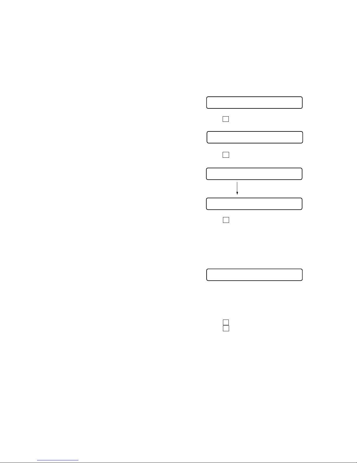
NV Reset
Caution: The shipment data will be cleared without the adjusted
values of the electrical offset adjustment and power supply adjustment when the NV is reset.
• Setting method of NV reset
1. Select the manual mode of the test mode, and set item number
021 NV Reset (see page 12).
2. Press the X key.
3. Press the X key once more.
4. Press the x key to quit the manual mode, and return to the
test mode (display check mode).
Temperature Correction
• Adjustment method of temperature correction
1. Select the manual mode of test mode, and set the item number
015 (see page 12).
2. Measure the ambient temperature.
3. Adjust with [VOL +], [VOL --] key so that the adjusted value
(hexadecimal value) becomes the ambient temperature.
(Initial value: 19h = 25 °C, Adjusting range: 80h to 7fh (–128
°C to +127 °C)
4. Press the X key to write the adjusted value.
5. Press the x key to quit the manual mode, and return to the
test mode (display check mode).
Note : Power supply adjustment auto item feed mode (see page
22 ) is available to perform the temperature correction and
power supply adjustment without entering the manual mode.
Remote commander LCD display
ResNV CC
021
Remote commander LCD display
ResOK?
021
Remote commander LCD display
NV reset (after several seconds)
Res***
021
Reset!
021
Remote commander LCD display
**
: Adjusted value
SetTmp@**
015
Page 18
18
MZ-N10
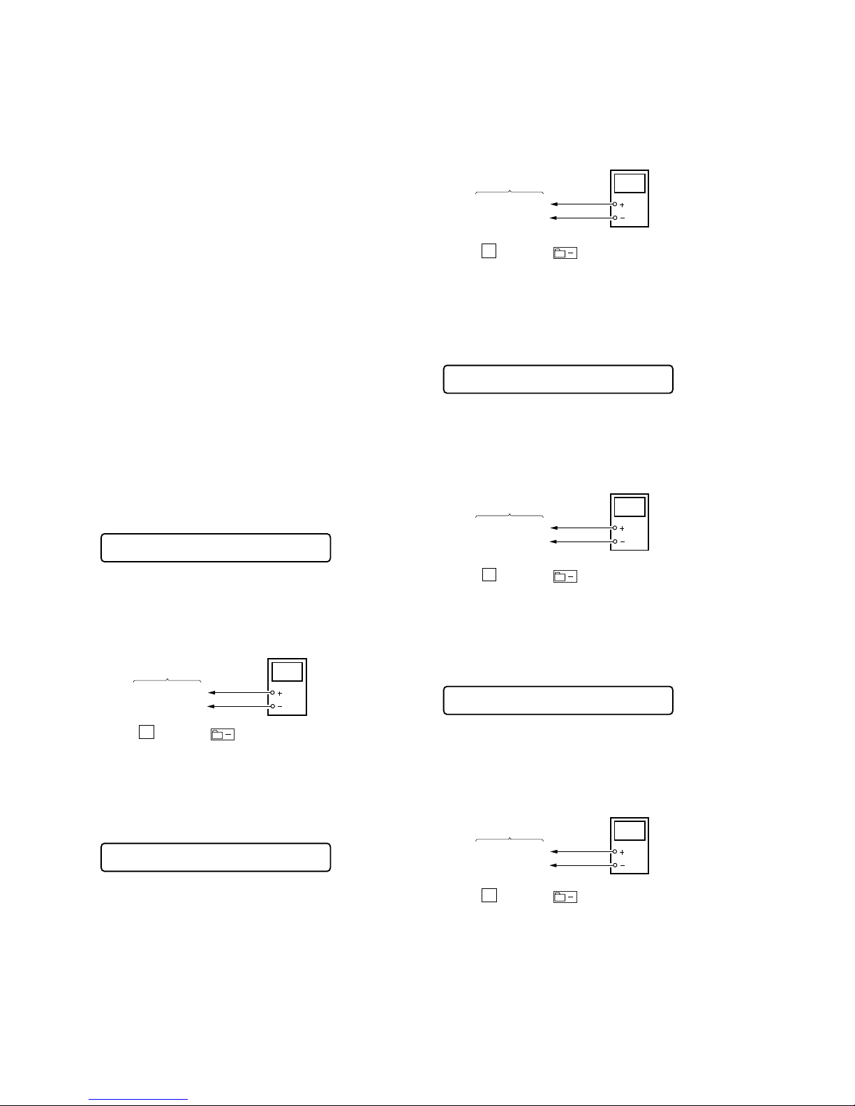
Power Supply Manual Adjustment
• Adjustment sequence
Adjustment must be done with the following steps.
1. VC1 Low adjustment (item number : 741)
2. VC1 High adjustment (item number : 742)
3. VC2 Low adjustment (item number : 743)
4. VC2 High adjustment (item number : 744)
5. REG1 adjustment (item number : 745)
6. REG3 Low (VC2 Low) adjustment (item number : 747)
7. REG3 Low (VC2 High) adjustment (item number : 748)
8. REG3 High adjustment (item number : 749)
9. VREC_Low adjustment (item number : 751)
10. VREC_Middle adjustment (item number : 752)
11. VREC_High adjustment (item number : 753)
12. 3.3upc adjustment (item number : 754)
13. ChgV L adjustment (item number : 755)
14. ChgV H adjustment (item number : 756)
• Setting method of power supply manual adjustment
1. Make sure that the power supply voltage is 6V(AC adaptor).
2. Select the manual mode of the test mode (see page 12).
3. Set item number.
Note : Power supply adjustment auto item feed mode (see page
12 ) is available to perform the temperature correction and
power supply adjustment without entering the manual mode.
• Adjustment method of VC1 Low
(item number: 741)
1. Connect a digital voltmeter to the TP1906 (VC1) on the MAIN
board, and adjust [VOL +] key (voltage up) or [VOL --] key
(voltage down) so that the voltage becomes 2.35 V.
2. Press the X key or the key on the remote commander
to write the adjusted value.
Adjustment and Connection Location: MAIN board
(see page 21)
• Adjustment method of VC1 High
(item number: 742)
1. Connect a digital voltmeter to the TP1906 (VC1) on the MAIN
board, and adjust
[VOL +] key (voltage up) or [VOL --] key
(voltage down) so that the voltage becomes 2.75 V.
2. Press the
X key or the key on the remote commander
to write the adjusted value.
Adjustment and Connection Location: MAIN board
(see page 21)
• Adjustment method of VC2 Low
(item number: 743)
1. Connect a digital voltmeter to the TP1936 (VC2) on the MAIN
board, and adjust [VOL +] key (voltage up) or [VOL --] key
(voltage down) so that the voltage becomes 1.25 V.
2. Press the
X key or the key on the remote commander
to write the adjusted value.
Adjustment and Connection Location: MAIN board
(see page 21)
• Adjustment method of VC2 High
(item number: 744)
1. Connect a digital voltmeter to the TP1936 (VC2) on the MAIN
board, and adjust [VOL +] key (voltage up) or [VOL --] key
(voltage down) so that the voltage becomes 1.70 V.
2. Press the X key or the key on the remote commander
to write the adjusted value.
Adjustment and Connection Location: MAIN board
(see page 21)
Remote commander LCD display
**
: Adjusted value
VC1 L **
741
digital
voltmete
r
MAIN board
TP1906 (VC1)
TP1951 (GND)
+ 0.005
– 0.000
Remote commander LCD display
**
: Adjusted value
VC1 H **
742
+ 0.005
– 0.000
digital
voltmete
r
MAIN board
TP1906 (VC1)
TP1951 (GND)
Remote commander LCD display
**
: Adjusted value
VC2 Lo **
743
+ 0.007
– 0.000
digital
voltmete
r
MAIN board
TP1936 (VC2)
TP1951 (GND)
Remote commander LCD display
**
: Adjusted value
VC2 Hi **
744
+ 0.007
– 0.000
digital
voltmete
r
MAIN board
TP1936 (VC2)
TP1951 (GND)
Page 19
19
MZ-N10
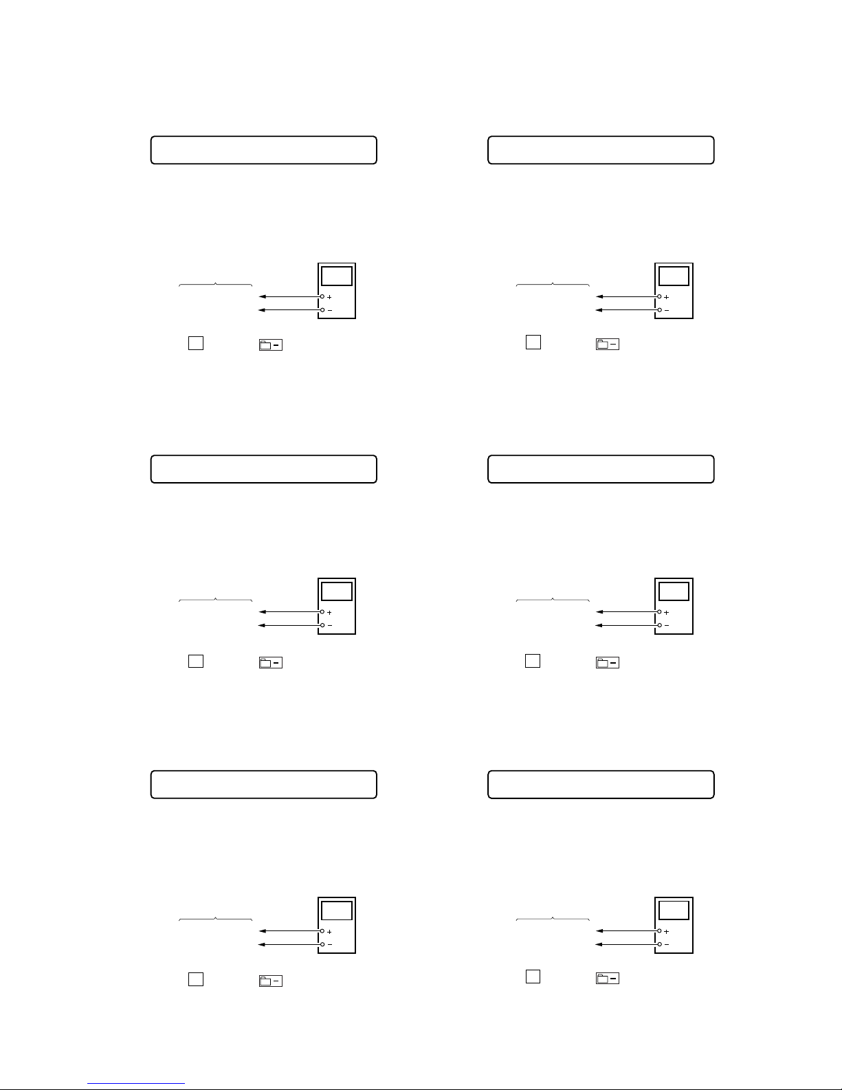
• Adjustment method of REG1
(item number: 745)
1. Connect a digital voltmeter to the
TP1909 (REG1)
on the MAIN
board, and adjust [VOL +] key (voltage up) or [VOL --] key
(voltage down) so that the voltage becomes 2.15 V.
2. Press the
X key or the key on the remote commander
to write the adjusted value.
Adjustment and Connection Location: MAIN board
(see page 21)
• Adjustment method of REG 3 Low (VC2 Low)
(item number: 747)
1. Connect a digital voltmeter to the
TP1907 (REG3)
on the MAIN
board, and adjust [VOL +] key (voltage up) or [VOL --] key
(voltage down) so that the voltage becomes 1.20 V.
2. Press the X key or the key on the remote commander
to write the adjusted value.
Adjustment and Connection Location: MAIN board
(see page 21)
• Adjustment method of REG 3 Low (VC2 High)
(item number: 748)
1. Connect a digital voltmeter to the
TP1907 (REG3)
on the MAIN
board, and adjust [VOL +] key (voltage up) or [VOL --] key
(voltage down) so that the voltage becomes 1.20 V.
2. Press the
X key or the key on the remote commander
to write the adjusted value.
Adjustment and Connection Location: MAIN board
(see page 21)
• Adjustment method of REG 3 High
(item number: 749)
1. Connect a digital voltmeter to the
TP1907 (REG3)
on the MAIN
board, and adjust [VOL +] key (voltage up) or [VOL --] key
(voltage down) so that the voltage becomes 1.35 V.
2. Press the
X key or the key on the remote commander
to write the adjusted value.
Adjustment and Connection Location: MAIN board
(see page 21)
• Adjustment method of VREC_Low
(item number: 751)
1. Connect a digital voltmeter to the
TP1622 (VREC)
on the MAIN
board, and adjust [VOL +] key (voltage up) or [VOL --] key
(voltage down) so that the voltage becomes 1.10 ± 0.015 V.
2. Press the
X key or the key on the remote commander
to write the adjusted value.
Adjustment and Connection Location: MAIN board
(see page 21)
• Adjustment method of VREC_Middle
(item number: 752)
1. Connect a digital voltmeter to the
TP1622 (VREC)
on the MAIN
board, and adjust [VOL +] key (voltage up) or [VOL --] key
(voltage down) so that the voltage becomes 1.24 ± 0.015 V.
2. Press the X key or the key on the remote commander
to write the adjusted value.
Adjustment and Connection Location: MAIN board
(see page 21)
Remote commander LCD display
**
: Adjusted value
REG1 **
745
+ 0.01
– 0.00
digital
voltmete
r
MAIN board
TP1909 (REG1)
TP1951 (GND)
Remote commander LCD display
**
: Adjusted value
REG3L1 **
747
+ 0.01
– 0.00
digital
voltmete
r
MAIN board
TP1907 (REG3)
TP1951 (GND)
digital
voltmete
r
MAIN board
TP1907 (REG3)
TP1951 (GND)
Remote commander LCD display
**
: Adjusted value
REG3L2 **
748
+ 0.01
– 0.00
+ 0.01
– 0.00
Remote commander LCD display
**
: Adjusted value
REG3 H **
749
digital
voltmete
r
MAIN board
TP1907 (REG3)
TP1951 (GND)
Remote commander LCD display
**
: Adjusted value
VREC L **
751
digital
voltmete
r
MAIN board
TP1622 (VREC)
TP1951 (GND)
Remote commander LCD display
**
: Adjusted value
VREC M **
752
digital
voltmete
r
MAIN board
TP1622 (VREC)
TP1951 (GND)
Page 20

20
MZ-N10
• Adjustment method of VREC_High
(item number: 753)
1. Connect a digital voltmeter to the
TP1622 (VREC)
on the MAIN
board, and adjust [VOL +] key (voltage up) or [VOL --] key
(voltage down) so that the voltage becomes 1.54 ± 0.015 V.
2. Press the
X key or the key on the remote commander
to write the adjusted value.
Adjustment and Connection Location: MAIN board
(see page 21)
• Adjustment method of 3.3upc
(item number: 754)
1. Remove the AC adaptor and USB cradle.
2. Turn off the BUILT-IN BATTERY switch.
3. Remove the rechargeable battery from the connector (CN951).
4. Supply dc 3.7V to the battery terminals (TP1952 : +, TP1951
: GND) with a regulated dc power supply.
5. Supply dc 5V to pin 8 (VBUS) of CN952 with a regulated dc
power supply.
6. Turn on the BUILT-IN BATTERY switch.
7. Select the manual mode of the test mode (see page 12), and set
the item number 754.
8. Connect a digital voltmeter to the
TP1623 (3.3upc)
on the MAIN
board, and adjust [VOL +] key (voltage up) or [VOL --] key
(voltage down) so that the voltage becomes 3.30 ± 0.01 V.
9. Press the
X key or the key on the remote commander
to write the adjusted value.
Adjustment and Connection Location: MAIN board
(see page 21)
• Adjustment method of ChgV L
(item number: 755)
Note : Remove the rechargeable battery from the connector
(CN951) and measure the voltage with the BUILT-IN BATTERY switch on. Use AC adaptor (6V) and USB cradle to
supply the power.
1. Connect a digital voltmeter to the TP1952 (ChgV) on the MAIN
board, and adjust
[VOL +] key (voltage up) or [VOL --] key
(voltage down) so that the voltage becomes 3.40 ± 0.024 V.
2. Press the
X key or the key on the remote commander
to write the adjusted value.
Adjustment and Connection Location: MAIN board
(see page 21)
• Adjustment method of ChgV H
(item number: 756)
Note : Remove the rechargeable battery from the connector
(CN951) and measure the voltage with the BUILT-IN BATTERY switch on. Use AC adaptor (6V) and USB cradle to
supply the power.
1. Connect a digital voltmeter to the TP1952 (ChgV) on the MAIN
board, and adjust [VOL +] key (voltage up) or [VOL --] key
(voltage down) so that the voltage becomes 4.20 ± 0.024 V.
2. Press the
X key or the key on the remote commander
to write the adjusted value.
Adjustment and Connection Location: MAIN board
(see page 21)
Remote commander LCD display
**
: Adjusted value
VREC H **
753
digital
voltmete
r
MAIN board
TP1622 (VREC)
TP1951 (GND)
Remote commander LCD display
**
: Adjusted value
3.3upc **
754
digital
voltmete
r
MAIN board
TP1623 (3.3upc)
TP1951 (GND)
Remote commander LCD display
**
: Adjusted value
ChgV L **
755
digital
voltmete
r
MAIN board
TP1952 (ChgV)
TP1951 (GND)
digital
voltmete
r
MAIN board
TP1952 (ChgV)
TP1951 (GND)
Remote commander LCD display
**
: Adjusted value
ChgV H **
756
Page 21
21
MZ-N10
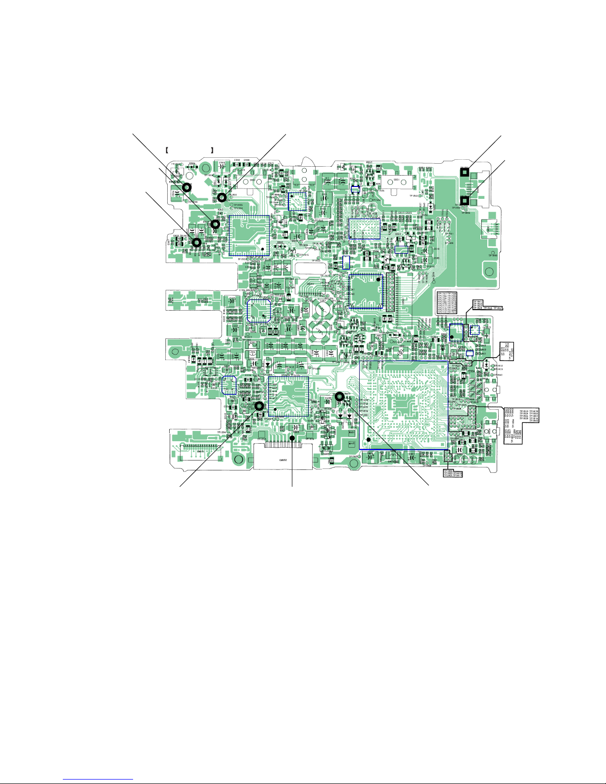
IC951
IC901
IC301
IC501
IC952
IC503
IC701
IC601
IC302
IC851
IC861
IC862
IC801
IC502
MAIN BOARD (SIDE B)
TP1951 (GND)
TP1952 (ChgV
)
TP1906 (VC1)
TP1936 (VC2)
TP1907 (REG3)
TP1909 (REG1)
TP1622 (VREC)
TP1623 (3.3upc)
(VBUS)
– MAIN Board (Side B) –
Adjustment/checking and Connection Location:
Page 22
22
MZ-N10
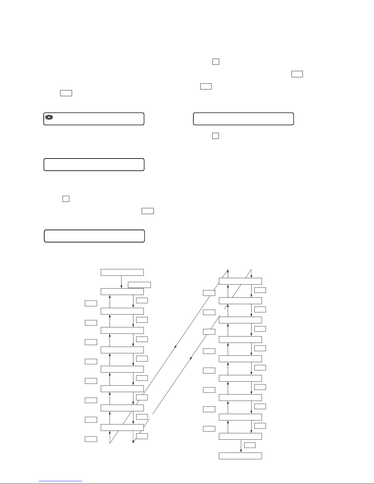
Power Supply Adjustment Auto Item Feed
Note :This mode is available to perform the temperature correc-
tion and power supply adjustment without entering the
manual mode.
• Setting method of power supply adjustment auto item
feed mode.
1. Set the test mode (see page 11)
2. Press the . or [VOL --] key to activate the overall adjust-
ment mode.
3. Turn the jog dial (up), or press the [P MODE] key on the
remote commander to set the temperature correction mode.
4. To change the initial value (hexadecimal), adjust with the [VOL
+] or [VOL --] key.
Press the X key to write the adjusted value, and the item
number increases automatically.
When not writing the adjusted value, press the > key to
move to the next item.
.
key
>
key
.
key
>
key
.
key
>
key
.
key
>
key
.
key
>
key
The jog dial (up) or
P MODE
key on the remote
commander
000Assy **
015 SetTmp 19
741 VC1 L **
742 VC1 H **
743 VC2 Lo **
744 VC2 Hi **
745 REG1 **
.
key
>
key
>
key
>
key
>
key
.
key
>
key
.
key
>
key
751 VREC L **
752 VREC M **
753 VREC H **
754 3.3upc **
.
key
>
key
755 ChgV L **
.
key
>
key
756 ChgV H **
.
key
>
key
757 CIL **
>
key
000 ADJ OK
.
key
.
key
>
key
746 REG2 **
747 REG3L1 **
>
key
.
key
748 REG3L2 **
749 REG3 H **
.
key
.
key
5. Connect a digital voltmeter to the test points on the MAIN
board, and adjust the voltage with the [VOL +] or [VOL --]
key. (see page 18 to 20)
Press the X key to write the adjusted value, and the item
number increases automatically.
6. When not writing the adjusted value, press the > key to
move to the next item.
The . key is available to back to the last item.
7. The following message is displayed after all power supply adjustments finish.
8. Press the x key to return to the test mode (display check
mode).
Remote commander LCD display
Assy**
000
Remote commander LCD display
**
: Adjusted value
SetTmp@**
015
Remote commander LCD display
**
: Adjusted value
VC1 L **
741
Remote commander LCD display
ADJ OK
000
Configuration of power supply adjustment auto item feed
Page 23
23
MZ-N10
Laser Power Check and Adjustment
Connection :
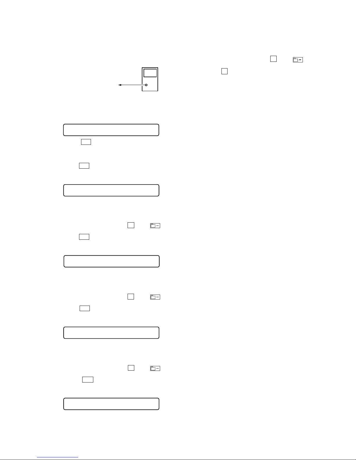
Checking and Adjustment Method :
1. Select the manual mode of test mode (see page 12), and set the
laser power adjusting mode (item number 010).
2. Press the . key continuously until the optical pick-up
moves to the most inward track.
3. Open the cover and set the laser power meter on the objective
lens of the optical pick-up.
4. Press the > key, and set the laser MO read adjustment mode
(item number 011).
5. Check that the laser power meter reading is 0.572 ± 0.10 mW.
6. If the reading value is not satisfied, adjust with the [VOL +] or
[VOL --] key so that the laser power meter reading becomes
the specification value. Press the X key or
key on the
remote commander to write the adjusted value.
7. Press the
> key, and set the laser CD read adjustment mode
(item number 012).
8. Check that the laser power meter reading is 0.763 ± 0.13 mW.
9. If the reading value is not satisfied, adjust with the [VOL +] or
[VOL --] key so that the laser power meter reading becomes
the specification value. Press the X key or
key on the
remote commander to write the adjusted value.
10. Press the
> key, and set the laser MO (×2 speed) write ad-
justment mode (item number 013).
11. Check that the laser power meter reading is 7.34 ± 0.88 mW.
12. If the reading value is not satisfied, adjust with the [VOL +] or
[VOL --] key so that the laser power meter reading becomes
the specification value. Press the X key or
key on the
remote commander to write the adjusted value.
13. Press the > key, and set the laser MO (x4 speed) write
adjustment mode (item number 014).
laser
power meter
Optical pick-up
objective lens
Remote commander LCD display
Laser
010
Remote commander LCD display
LrefPw@**
011
Remote commander LCD display
HrefPw@**
012
Remote commander LCD display
WrPwLo@**
013
Remote commander LCD display
WrPwHi@**
014
14. Check that the laser power meter reading is 8.81 ± 1.05mW.
15. If the reading value is not satisfied, adjust with the [VOL +] or
[VOL --] key so that the laser power meter reading becomes
the specification value. Press the X key or
key on the
remote commander to write the adjusted value.
16. Press the x key to quit the manual mode, and activate the test
mode (display check mode).
Page 24
24
MZ-N10
Overall Adjustment Mode
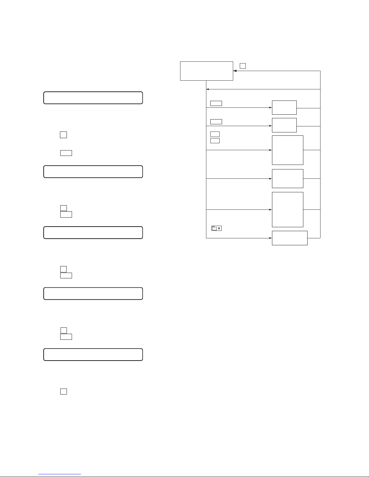
• Configuration of overall adjustment mode
Adjustment required before Overall Adjustment
Note : Modify five adjusted values through the following proce-
dure before performing the CD overall adjustment and MO
overall adjustment.
• Adjusted values modifying procedure
1. Select manual mode of the test mode, and set item number
822 (see page 12).
2. Adjust with the [VOL +] key (adjusted value up) or [VOL --]
key (adjusted value down) so that the adjusted value becomes
03.
3. Press the X key to write the adjusted value.
4. Select manual mode of the test mode, and set item number
870 (see page 12).
5. Press the > key to set item number 875.
6. Adjust with the [VOL +] key (adjusted value up) or [VOL --]
key (adjusted value down) so that the adjusted value becomes
3E.
7. Press the X key to write the adjusted value.
8. Press the > key to set item number 876.
9. Adjust with the
[VOL +] key (adjusted value up) or [VOL --]
key (adjusted value down) so that the adjusted value becomes
00.
10. Press the X key to write the adjusted value.
11. Press the > key to set item number 881.
12. Adjust with the [VOL +] key (adjusted value up) or [VOL --]
key (adjusted value down) so that the adjusted value becomes
37.
13. Press the X key to write the adjusted value.
14. Press the > key to set item number 882 .
15. Adjust with the [VOL +] key (adjusted value up) or [VOL --]
key (adjusted value down) so that the adjusted value becomes
E0.
16. Press the X key to write the adjusted value.
Remote commander LCD display
**
: Adjusted value
###S **
822
Remote commander LCD display
**
: Adjusted value
###S **
875
Remote commander LCD display
**
: Adjusted value
###S **
876
Remote commander LCD display
**
: Adjusted value
###S **
881
Remote commander LCD display
**
: Adjusted value
###S **
882
Overall adjustment mode
(Title display)
"Assy**"
Continuing overall adjustment
x
key
.
key
>
key
CD overall
adjusting
MO overall
adjusting
Electrical
offset
adjustment
NV reset
(item number 21)
Automatic
Disc
discrimination
overall
adjustment
Temperature
correction
and
Power supply
adjustment
auto item feed
Jog dial (down) or
[DISPLAY]
key
on the remote commander
Jog dial (up) or
[P MODE]
key
on the remote commander
[GROUP]
key or
key
on the remote commander
N
key or
u
key
on the remote commander
Page 25
25
MZ-N10
Note: Adjust the CD first, when performing adjustment.
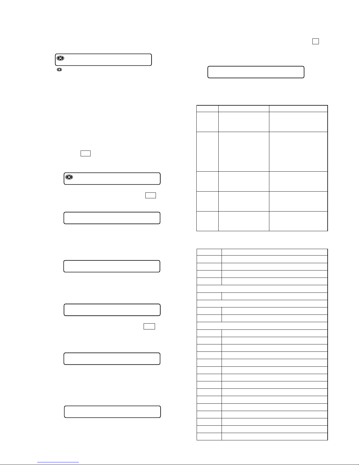
• Adjustment method of CD and MO overall adjustment
mode
1. Set the test mode (see page 11).
2. Press the . or [VOL --] key to activate the overall adjust-
ment mode.
3. Insert CD disc in the set, and press thethe . key to set the
CD overall adjustment mode. Automatic adjustments are made.
4. In case of CD overall adjustment NG, readjust from the NV
reset (see page 17). The temperature correction (see page 17)
may be omitted.
5. If OK through the CD overall adjustments, then perform MO
overall adjustments.
6. Insert MO disc in the set, and press the > key to set the
MO overall adjustment mode. Automatic adjustments are
made.
7. In case of MO overall adjustment NG, readjust from the NV
reset (see page 17). The temperature correction (see page 17)
may be omitted.
• Overall adjustment mode (title display)
Remote commander LCD display
: (Disc mark) At end of power supply adjustment: Outside lit
**
: Left side = MO overall adjustment information
F*
: MO overall adjustment completed
1*
: Manual adjustment exists (overall adj. not completed)
0*
: Not adjusted
Right side = CD overall adjustment information
*F
: CD overall adjustment completed
*1
: Manual adjustment exists (overall adj. not completed)
*0
: Not adjusted
Assy**
000
8. If OK through the MO overall adjustments, press the x key
to return to the test mode and terminate the overall adjustment
mode.
Remote commander LCD display
Assy11
000
Remote commander LCD display
XXX
: Item number for which an adjustment is being executed.
CD RUN
XXX
Remote commander LCD display
**
: NG item number.
*** NG
000
Remote commander LCD display
CD OK
000
Remote commander LCD display
XXX
: Item number for which an adjustment is being executed.
MO RUN
XXX
Remote commander LCD display
**
: NG item number.
*** NG
000
Remote commander LCD display
MO OK
000
• Overall Adjustment error message
The following message will be displayed if adjustment
procedure is mistaken in the CD and MO overall adjustment.
Message Display timing
During CD/MO/DISC
CLOSE! automatic distinction
overall adjustment
During MO/DISC
Set CD!
automatic distinction
overall adjustment
During offset adjustment
Set MO! During offset adjustment
During CD/MO/DISC
NoTmp! automatic distinction
overall adjustment
During CD/MO/DISC
NoChg! automatic distinction
overall adjustment
Description
DISC is not inserched.
• CD overall adjustment is not
completed in the MO overall
adjustment.
• CD and MO overall
adjustment is not completed
in the offset adjustment.
MO overall adjustment is not
completed in the offset
adjustment.
Temperature correction
(item number 015)
is not finished.
Charge voltage adjustments
(item number 755 and 756)
are not finished.
• CD and MO Overall Adjustment Items
1. CD overall adjustment items
Item No. Description
761 VC,VR power supply H/L selection
300 HPIT setting • servo OFF
561 SLED inward movement
562 SLED outward movement
High reflection electrical adjustment
312 Laser ON • Focus UP • vc correction
ALFA offset adjustment
313 IJ offset adjustment
314 FE offset adjustment
HPIT adjustment
320 Focus servo ON
324 TE offset adjustment 1
321 TE gain adjustment
328 TWPP gain adjustment
324 TE offset adjustment 1
332 TE offset adjustment 2
330 Tracking servo ON
336 ABCD gain adjustment
337 KF gain correction
338 RF gain adjustment
344 FCS gain adjustment
345 TRK gain adjustment
521 Two-axis sensitivity (inner position)
522 Two-axis sensitivity (outer position)
300 HPIT setting • servo OFF
Page 26
26
MZ-N10
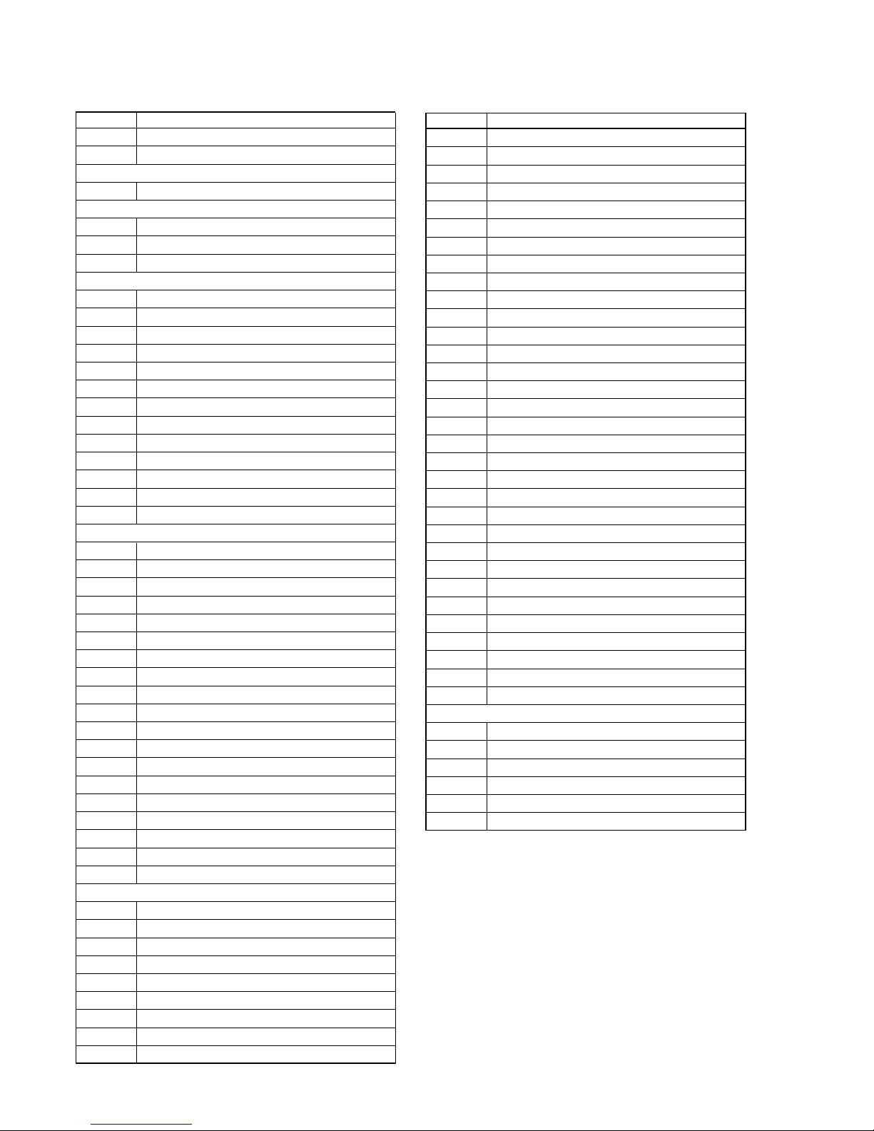
2. MO overall adjustment items
Item No. Description
716 VC,VR power supply H/L selection
100 R_GRV setting • servo OFF
Low reflection electrical offset adjustment
112 Laser ON • Focus UP vc correction
ALFA offset adjustment
113 IJ offset adjustment
114 FE offset adjustment
118 Wpp denominator offset adjustment
LPIT adjustment
200 LPIT setting • servo OFF
561 SLED inward movement
220 Focus servo ON
224 TE offset adjustment 1
221 TE gain adjustment
224 TE offset adjustment 1
232 TE offset adjustment 2
230 Tracking servo ON
236 ABCD gain adjustment
237 KF gain correction
238 RF gain adjustment
244 Focus gain adjustment
245 Tracking gain adjustment
READ GRV adjustment 1
100 R_GRV setting • servo OFF
562 SLED outward movement
120 Focus servo ON
122 TON offset adjustment
121 TE gain adjustment
122 TON offset adjustment
123 TEIN offset adjustment
124 TWPP offset adjustment 1
130 Tracking servo ON
131 TWPP offset adjustment 1
136 ABCD gain adjustment
137 KF gain correction
139 ADIP BPF f0 adjustment
144 Focus gain adjustment
145 Tracking gain adjustment
134 TWPP gain adjustment
131 TWPP offset adjustment 1
132 TWPP offset adjustment 2
149 TWPP OP offset adjustment
WRITE GRV adjustment
410 HEAD DOWN • GRV servo ON
420 READ t WRITE selection
421 TE gain adjustment
423 TEIN offset adjustment
430 Tracking servo ON
431 TWPP offset adjustment 1
436 ABCD gain adjustment
444 Focus gain adjustment
445 Tracking gain adjustment
Item No. Description
434 TWPP gain adjustment
431 TWPP offset adjustment 1
432 TE offset adjustment 2
449 TWPP OP offset adjustment
410 READ t WRITE selection
411 TWPP offset adjustment 1
412 TE offset adjustment 2
418 TWPP OP offset adjustment
490 HCLV t LCLV selection process
450 HEAD DOWN • GRV servo ON
460 READ t WRITE selection
461 TE gain adjustment
463 TEIN offset adjustment
470 Tracking servo ON
471 TWPP offset adjustment 1
476 ABCD gain adjustment
484 Focus gain adjustment
485 Tracking gain adjustment
451 TWPP offset adjustment 1
452 TE offset adjustment 2
460 READ t WRITE selection
470 Tracking servo ON
474 TWPP gain adjustment
471 TWPP offset adjustment 1
472 TE offset adjustment 2
489 TWPP OP offset adjustment
450 WRITE t READ selection
451 TWPP offset adjustment 1
452 TE offset adjustment 2
458 TWPP OP offset adjustment
448 30 sec continuous REC
400 GRV setting • servo OFF • HEAD UP
READ GRV adjustment 2
120 Focus servo ON
130 Tracking servo ON
138 RF gain adjustment
141 FOCUS_BIAS
035 Stray light offset measurement
100 R_GRV setting • servo OFF
Page 27
27
MZ-N10
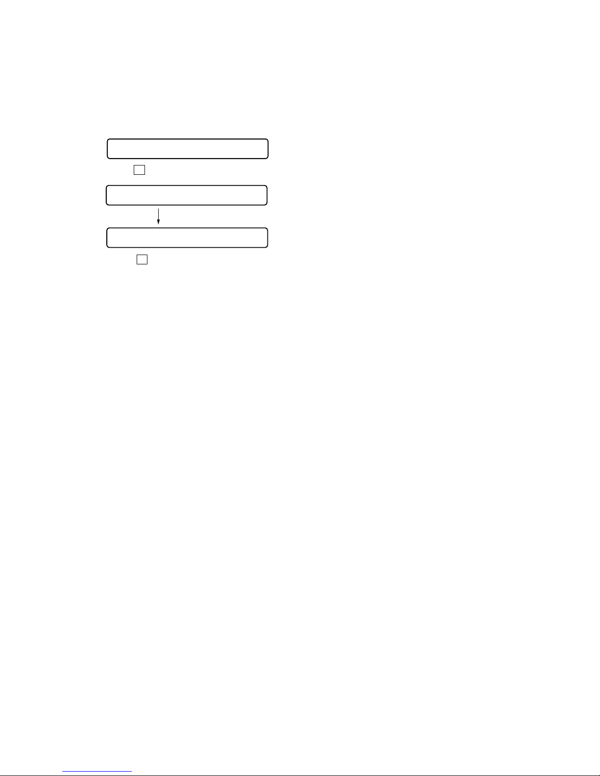
Resume Clear
Perform the Resume clear when all adjustments completed.
• Resume clear setting method
1. Select the manual mode of the test mode, and set item number
043 (see page 12).
2. Press the X key.
3. Press the x key to return to the test mode (display check
mode).
Remote commander LCD display
Resume 00
043
Remote commander LCD display
Resume clear complete
Res***
043
ResClr
043
Page 28
28
MZ-N10
Rewriting the Patch Data at Replacement of Main Board
This set requires the patch data in the nonvolatile memory (IC851) to be rewritten using the application, when the MAIN board was
replaced.
Caution: The application that meets the microcomputer version in this set must be used when rewriting the patch data. Rewriting the
patch data using the application not suitable for the microcomputer version could cause the set to malfunction.
For a checking method of the microcomputer version, see “SECTION 4 TEST MODE” (page 11).
•Preparation
1. USB cradle (attached to the set)
2. USB cable (attached to the set)
3. Personal computer in which the Net MD Driver has been installed. (For further information, see “System requirements” (page 4) in
“SECTION 1 SERVICING NOTES”)
4. Application “PatchWriter” for patch data rewriting
•How to get the application “PatchWriter” for patch data rewriting
Contact our service technical support section for PA products to get the application.
• Pre-check
1. Check the microcomputer version in this set. (For a checking method of the microcomputer version, see “SECTION 4 TEST MODE”
(page 11).)
2. Check that the Net MD Driver has been installed in the personal computer.
3. Make sure that the set is in the Normal mode.
Note: Do not rewrite the patch data in the Test mode.
•Rewriting the patch data
1. Connect the USB cradle to the personal computer with the USB cable, and place the set on the USB cradle.
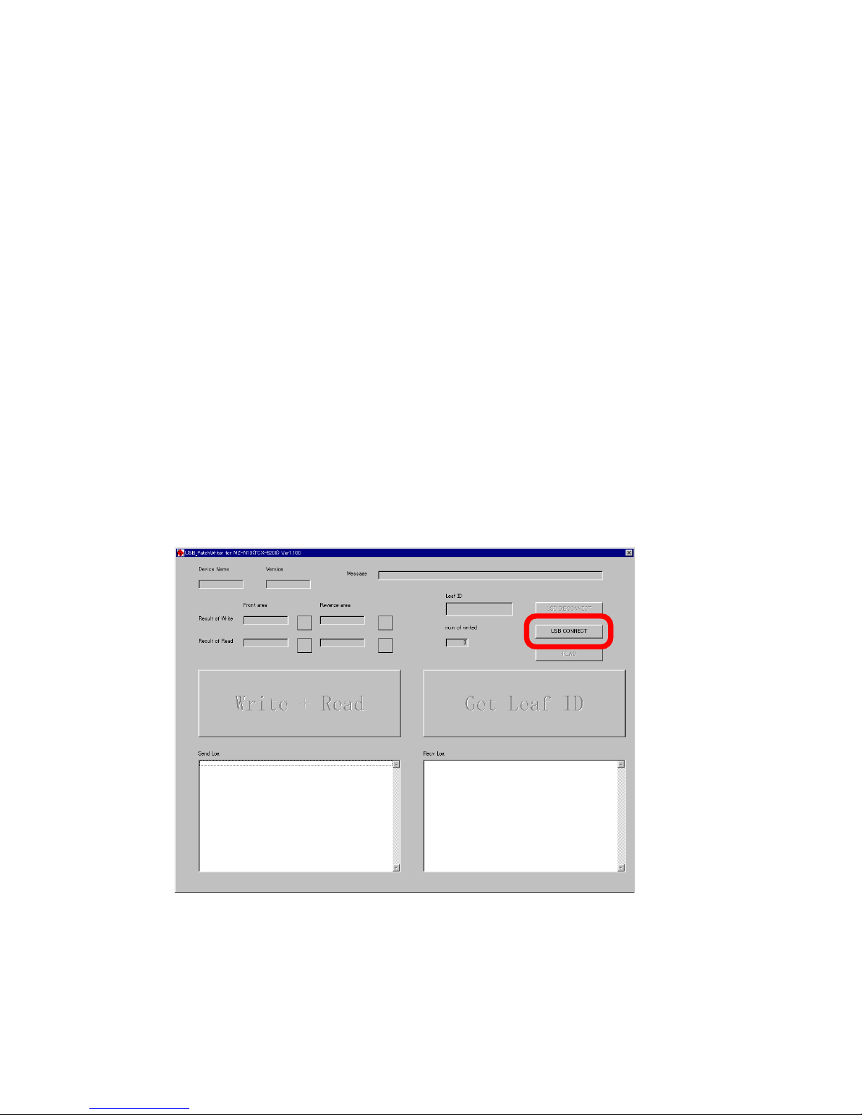
2. Start the application “PatchWriter”.
3. Make sure that the following window opens.
4. Click the [USB CONNECT] button.
Page 29
29
MZ-N10
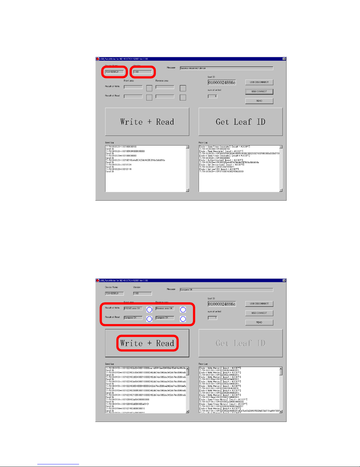
5. Confirm that the model and version indicated on the title bar coincide with the codes displayed in the Device Name block and the
Ve r sion block in the window.
6. Click the [Write + Read] button.
The patch data writing and the verify processing will be executed automatically in the following order:
1) Writing to patch area (front area)
2) Writing to patch area (reverse area)
3) Verifying patch area (front area)
4) Verifying patch area (reverse area)
7. The operation will terminate with the a (blue) mark given to all areas.
If the × (red) mark is given to any area, the nonvolatile memory will be faulty.
Page 30
30
MZ-N10
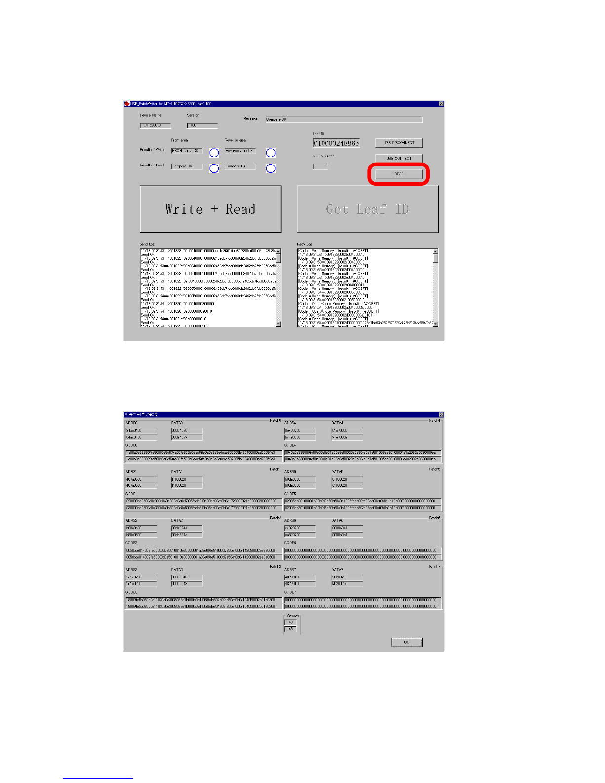
• Confirmation of contents of the patch data rewrited
1. Click the [READ] button to confirm the contents of the patch data rewrited.
2. The application reads out the front and reverse patch areas and displays the results in the edit box.
Confirm that the upper column coincides with the lower column as the following window.
3. Click the [OK] button to close the window.
Page 31
31
MZ-N10
• Removing the set
Remove the set as following procedure after rewriting the patch data and confirmation.
Note : When the following procedure is not completed but USB cable is extracted, the application does not recognize the set at exchanging
the set.
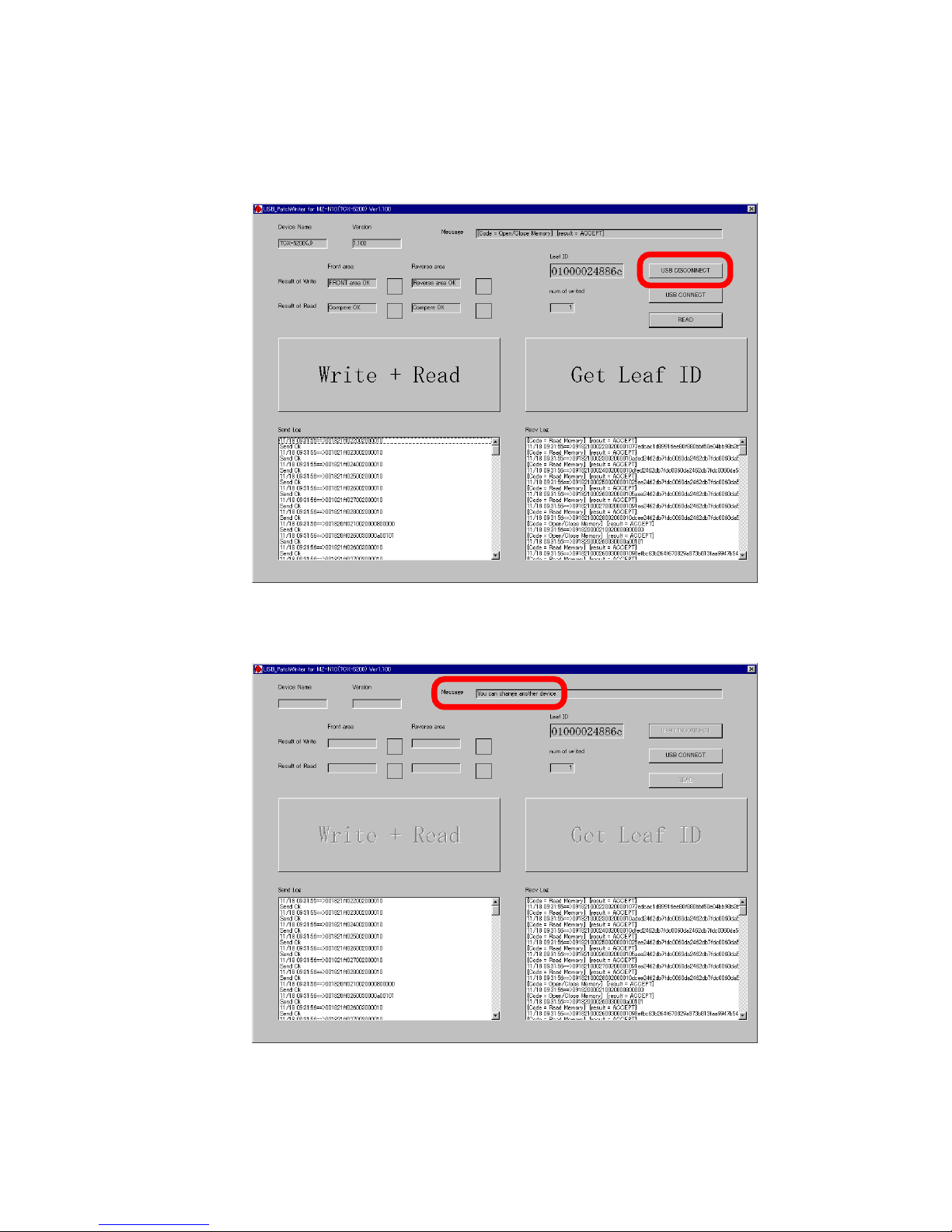
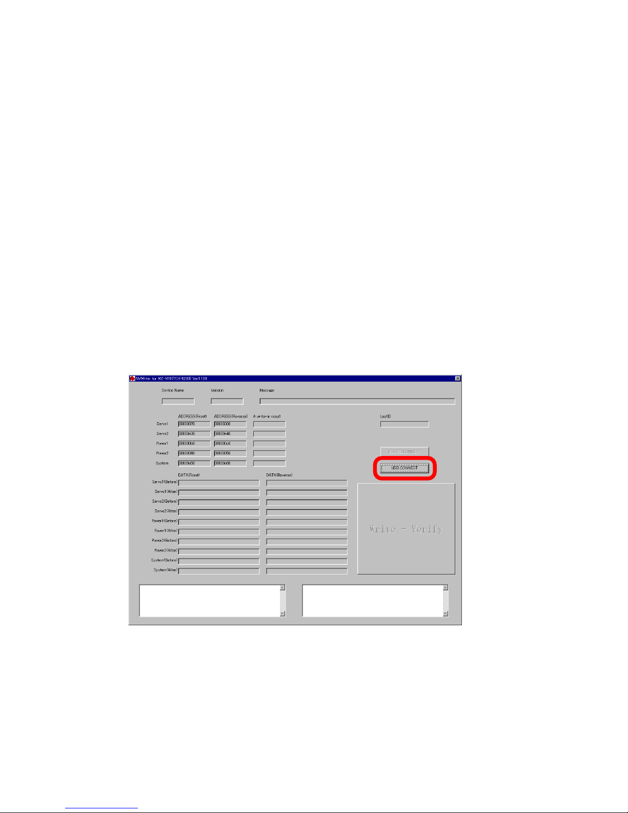
1. Click the [USB DISCONNECT] button.
2. Confirm that "You can change another device" is displayed in the message block.
3. Disconnect the USB cable from the personal computer and the USB cradle.
4. Remove the set from the USB cradle.
Page 32
32
MZ-N10
Rewriting the NV values
Caution: The application that meets the microcomputer version in this set must be used when rewriting the NV values. Rewriting the NV
values using the application not suitable for the microcomputer version could cause the set to malfunction.
For a checking method of the microcomputer version, see “SECTION 4 TEST MODE” (page 11).
•Preparation
1. USB cradle (attached to the set)
2. USB cable (attached to the set)
3. Personal computer in which the Net MD Driver has been installed. (For further information, see “System requirements” (page 4) in
“SECTION 1 SERVICING NOTES”)
4. Application “NVWriter” for NV values rewriting
•How to get the application “NVWriter” for NV values rewriting
Contact our service technical support section for PA products to get the application.
• Pre-check
1. Check the microcomputer version in this set. (For a checking method of the microcomputer version, see “SECTION 4 TEST MODE”
(page 11).)
2. Check that the Net MD Driver has been installed in the personal computer.
3. Make sure that the set is in the Normal mode.
Note: Do not rewrite the NV values in the Test mode.
•Rewriting the NV values
1. Connect the USB cradle to the personal computer with the USB cable, and place the set on the USB cradle.
2. Start the application “NVWriter”.
3. Make sure that the following window opens.
4. Click the [USB CONNECT] button.
Page 33
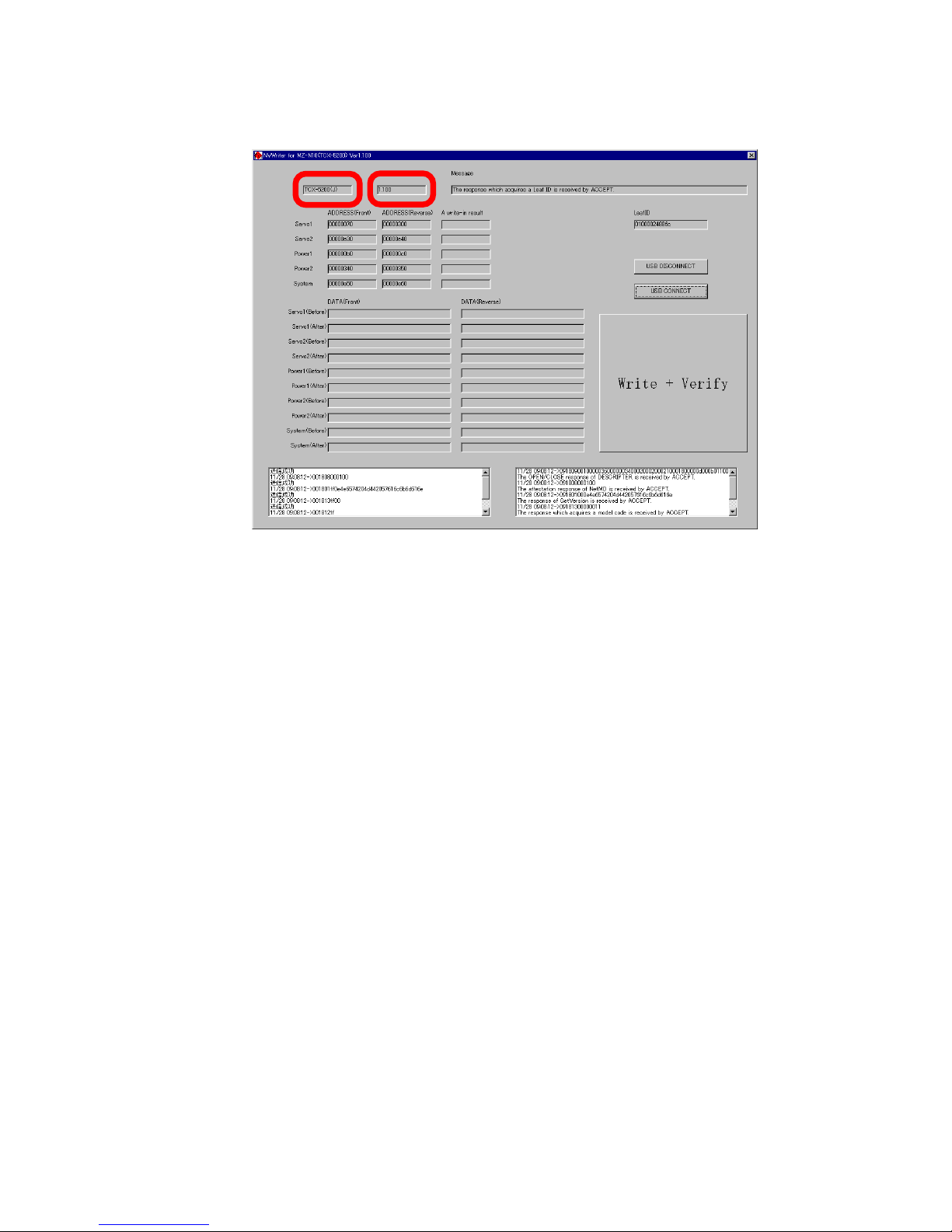
33
MZ-N10
5. Confirm that the model and version indicated on the title bar coincide with the codes displayed in the Device Name block and the
Ve r sion block in the window.
6. Click the [Write + Verify] button.
The NV values writing and the verify processing will be executed automatically in the following order:
1) Writing to Servo 1 area (front area)
2) Writing to Servo 1 area (reverse area)
3) Writing to Servo 2 area (front area)
4) Writing to Servo 2 area (reverse area)
5) Writing to Power Supply 1 area (front area)
6) Writing to Power Supply 1 area (reverse area)
7) Writing to Power Supply 2 area (front area)
8) Writing to Power Supply 2 area (reverse area)
9) Writing to System area (front area)
10) Writing to System area (reverse area)
11) Verifying to Servo 1 area (front area)
12) Verifying to Servo 1 area (reverse area)
13) Verifying to Servo 2 area (front area)
14) Verifying to Servo 2 area (reverse area)
15) Verifying to Power Supply 1 area (front area)
16) Verifying to Power Supply 1 area (reverse area)
17) Verifying to Power Supply 2 area (front area)
18) Verifying to Power Supply 2 area (reverse area)
19) Verifying to System area (front area)
20) Verifying to System area (reverse area)
Page 34
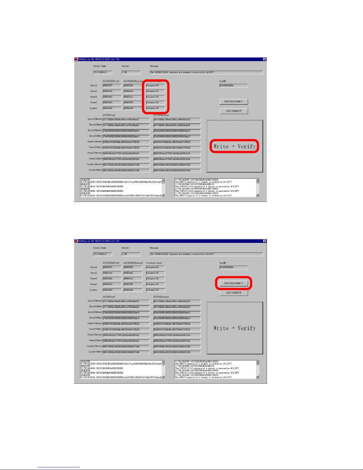
34
MZ-N10
7. The operation will terminate with “Compere OK” given to all areas.
If “Compere NG” is given to any area, the nonvolatile memory will be faulty.
8. Click the [USB DISCONNECT] button.
Page 35
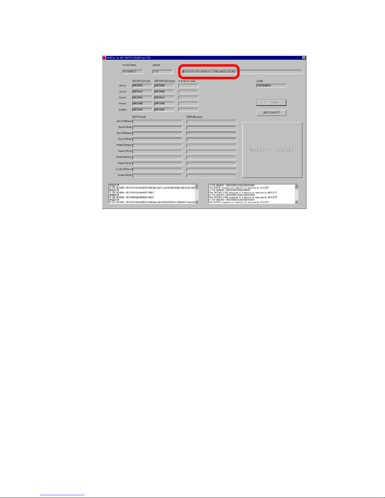
35
MZ-N10
9. Confirm that the window becomes as shown below where the [Write + Verify] button is inactive.
10. Disconnect the USB cable from the personal computer and the USB cradle.
11. Remove the set from the USB cradle.
Page 36

36
MZ-N10
Charging Information Clear of Built-in Lithium-ion
Rechargeable Battery
Function of recording the charging information is equipped for
design confirmation.
There are two informations only for buit-in lithium-ion rechargeable battery.
• Remaining charging time
• The number of times of fully charging
Initialization of the information is required at replacement of builtin rechargeable battery since it is pequliar to the buit-in lithiumion rechargeable battery.
Perform the initialization as the following procedure.
1. Select the manual mode of the test mode, and set item number
043 (Resume clear and time set clear).
2. Adjust with the [VOL +] key so that the adjusted value becomes 02, and press the X key or
key on the remote
commander.
3. Resume clear is completed when the following display appears.
4. Press the x key to return to the test mode (display check
mode).
Remote commander LCD display
Resume 00
043
adjusted value
Remote commander LCD display
**** 02
043
Remote commander LCD display
ResClr
043
Page 37
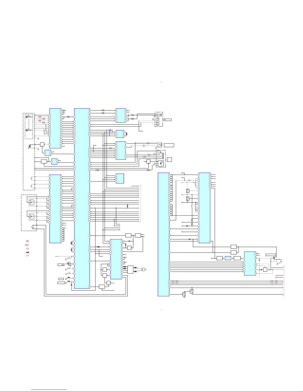
3737
MZ-N10
SECTION 6
DIAGRAMS
6-1. Block Diagram
OPTICAL PICK-UP
BLOCK
LDA
FOCUS
COIL
TRACKING
COIL
MOTOR/COIL DRIVE
IC701
FO2
30
RO2
32
13
11
TRK+
TRK-
FCS+
FCS-
28
FI2
RF AMP
IC501
11
AVCC2
VREF
7
ly
56
A
50
B
51
C
52
48
PEAK
LINE IN
(OPT)
58
VC
FO1
RO1
D
49
J302
MIC
(PLUG IN POWER)
J301
RFI
10
4
AOUT L
• Signal Path
: PLAYBACK
: DIGITAL IN
VREF
ly
lx
jy
jx
A
B
C
D
MON
GND
APC
Q501
LDK
5
2
3
VOL
DET
IC503
UNREG
A-C
16
D-C
15
lx
1
jy
55
jx
54
PDI
12
PDO
14
53AVCC
29DVCC
9
RFO
40
RFI
47
BOTM
41
ABCD
42
FE
43
TE
23
ADFG
13
PD NI
8
VC
18
SMON
33
SBUS
32
SCK
26CLK
FS256
35
RESET
REGO1
REG
Q502,503
VCC
5
2
3
VOL
DET
IC502
VC1
MD VCC
PDS0
PDS1
SLED
MOTOR
M602
M601
M603
26
COM2
35
UO2
SLED N
SLED U
SLED V
SLED W
25
CPUI2
37
VO2
24
CPVI2
39
WO2
23
CPWI2
SPINDLE
MOTOR
17
COM1
8
UO1
CLV N
CLV U
CLV V
CLV W
18
CPUI1
6
VO1
19
CPVI1
4
WO1
20
CPWI1
M
HD
MOTOR
HD DRV+
HD DRV-
MINI DISC
MECHANISM BLOCK
27
RI2
15
FI1
16
RI1
44
PWM2
43
UI2
42
VI2
41
WI2
45
CPUO2
46
CPVO2
47
CPWO2
55
PWM1
56
UI1
1
VI1
2
WI1
54
CPUO1
53
CPVO1
52
CPWO1
REGO1
51
VG
VGH
14VMF1
UNREG
29VMF2
18
VMR1
33
VMR2
9
VMU1
34
VMU2
5
VMVW1
38
VMVW2
DSP/DSSP
IC801(1/2)
SSB DATA
156
SSB CLK
157
XRF RST
130
PEAK
15
BOTM
16
ABCD
17
FE
18
TE
23
ADFG
28
APC REF
29
VC
19
SE
22
OPVCC CTL
110
RECP
70
PDS0
114
PDS1
115
TFDR
31
109
MDVCC CTL
TRDR
30
FFDR
32
FRDR
33
SFDDR
35
SLD MON
121
SRDR
48
SLD V
43
SLD W
44
SLC U
45
SLC V
46
SLC W
47
SPFD
37
SPDL MON
137
SRRD
36
SPD V
38
SPD W
39
SPC U
40
SPC V
41
SPC W
42
48
DE
XRST MTR DRV
143
6
VCC1
VCO1
8
VCC2
VCO2
L IN
3
R IN
15
AOUT R
BEEP
14104
BEEP
HP/L
16107
AOUT SEL
MUTE
1598
XMUTE
10L OUT
9
GAL
12
R OUT
13
GAR
HP AMP
IC302
7
SIO
1
RTC
IC862
SCLK
2
CE
12
8
X861
32.768kHz
100
SI0
101
SO0
102
SCK0
201CS RTC
IC861
42
1
SO
2
EEPROM
IC851
SI
5
SCK
126
XCS
1144
XCS NV
CDTI
11
18PRE L
A/D CONV & MIC AMP
IC301
CCLK
12
SDTO
751
ADDT
BCLK
853
XBCK
MCLK
954
FS256
LRCK
1052XRCK
CSN
1394XCS ADC
PDN
1495XPD ADC
19PRE R
28
L IN
1
R IN
FS256
REG
Q301
/ LINE OUT
J303
REGO1
105
XOPT CTL
49D IN
90
OPT DET
91
XJACK DET
92
XMIC DET
VCO1
169
RMC KEY
175
RMC DTCK
152
JOG A
153
JOG B
170
JOG PUSH
166WK DET
88PHASE KEY
197
VBUS 5V DET
162
SET KEY1
163
SET KEY2
171
REC KEY
108
REC OPR LED
128
CHG LED
142LCD STB
97
LCD RST
141XCS LCD
REGO1
VCOO1
DVDD
SIO
SDO
JOG A
JOG PUSH
XWK1
PHASE
SET KEY1
SET KEY2
REC
REC LED
CHG LED
STB
RST
CS
WK DET
REC KEY
SCK
JOG B
SDO0
SCK0
DATA
28
52
VREG33R
REC DRIVER
IC601
SCK
19
EFM
23
CLK
18
LATCH
21
XWAKEO
31
33DC IN
17
VIF
BUFFER
Q607
SW
Q608
BUFFER
Q612
71
EFMO
34
FS4
150
XCS REC DRV
4FS
VREG33
53292
USB IF VDD
51VREG33U
45
VBUS2
VCO1
VBUS
REGO1
63
VG
VGL
28
VG2
15VREF IN
VREF
56VBUS REF
SW
Q603
L1 1
7
L1 2
10
DW BT
4
SW
Q604
DW TP
5
BUFFER
Q606
SW
Q605
UNREG
112
VREC CTL
HALF LOCK SW
168
OPEN CLOSE SW
93
XHOLD SW
132
S801
S802
HOLD
S803
(OPEN/CLOSE)
PROTECT
89
S804
(PROTECT)
OSCI
1
OSCO
2
UOSCI
179
UOSCO
180
X801
22.5792MHz
X802
48MHz
HALF LOCK
(HALF LOCK)
T MARK SW
151
S805
T MARK
END SEARCH
172
S806
END SEARCH
VGH
30
HA
26
HB
29
HAB
25
HBB
SWITCH
Q601,602
58
OUT B
61
OUT A
: ANALOG IN
: RECORD
264
IFVDD0
DSP/DSSP
IC801(2/2)
TO
SWICH
&
LCD
MODULE
266
IFVDD1
268
IFVDD2
270
IFVDD3
272
IFVDD4
278
DAVDD
280
AVD1
282
AVD2
285
TSLVDD
293MVDD
294USB OSC VDD
299FVDD0
303DRAMVDD3
304DRAMVDD4
254
DVDD0
256
DVDD1
258
DVDD2
260
DVDD3
262DVDD4
301DVDD5
302DVDD6
284
TMSVDD
274
AVDD
REGO1
REGO1
43
58
DATA
POWER AMP
IC901
REGO3
39
VCO1
11
VC1
10
REGI1
44
L1
13
L1
14
VC1G
16
L904
Q901
L903
VC2G
32
Q902
HVB
8
L2
34
L2
35
VC1N
38
L902
VC2
42
REGI3
40
L901
VC1
UNREG
VC02
LG
24
CIL
22
VSTB
9
VREF
48
VGL
VG
23
VGH
VREF
D901
D904
D903
212XRST
123
SLEEP
138
XCS PWR IC
XRST2
27
SLEEP
64
STRB
59
D982
RMC KEY
XWAKE4
2
XWAKE3
3
XWAKE2
4
XWAKE1
5
SDO0
SCK0
4FS
HALF LOCK
RMC KEY
REC KEY
60
SCK
63
CLK
125CHGI CTL1
OVER
WRITE
HEAD
145CHG PWM
134CHG AD SEL
135CHGI SEL
160CHG MON
113
XRST CHGI IC
6VI2
REGO1
WK DET
14
BATT CHARGE
IC951
BUFFER
Q953
1
2
VOL
DET
IC952
WK UP SW
Q951
WK DET
VCO1
176
UDM
175
UDP
164
CRADLE DET
167BATT MON
111
BATT CTL
Q952
(2/2)
Q952
(1/2)
I CTL1
16
CHG CTL
20
AD SEL
5
ISEL
4
A/D
3
VI2 DET
2
12
VG
VGH
8
VBAT
23IN118RF1
7VO
24
VI
SW
Q954
124
FFCLR
BUFFER
Q961
BUFFER
Q904
1
FFCLR
UNREG
BATT 3.3V
DC IN6V
DATA+
DATA-
CRADLE DET
BATT MON
BATT CTL
VBUS
VGH
VBUS
VGH
TO
USB
CRADLE
S951
BUILT IN BATTERY
RECHARGEABLE BATTERY
LIP-3WMB, 3.7V, 340mAh,
Li-ion
OFF
ON
OFF
ON
: USB
Page 38
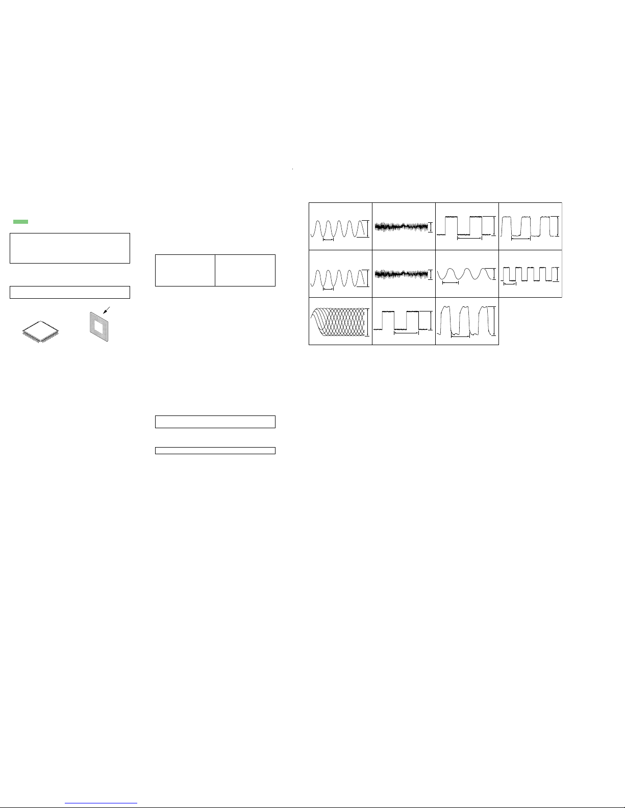
3838
MZ-N10
Note on Schematic Diagram:
• All capacitors are in µF unless otherwise noted. pF: µµF
50 WV or less are not indicated except for electrolytics
and tantalums.
• All resistors are in Ω and 1/
4
W or less unless otherwise
specified.
•%: indicates tolerance.
•f: internal component.
• C : panel designation.
• A : B+ Line.
•Total current is measured with MD installed.
•Power voltage is dc 6 V and fed with regulated dc power
supply from TP1976(+),TP1953(-) on MAIN board.
+side :TP1976(CN952 q;pin)
-side :TP1953(CN952 1pin)
•Voltages and waveforms are dc with respect to ground in
playback mode(servo on).
no mark : PLAYBACK(SERVO ON)
∗
: Impossible to measure
•Voltages are taken with a VOM (Input impedance 10 MΩ).
Voltage variations may be noted due to normal production tolerances.
•Waveforms are taken with a oscilloscope.
Voltage variations may be noted due to normal production tolerances.
• Circled numbers refer to waveforms.
• Signal path.
J : PLAYBACK
c : DIGITAL IN
F : ANALOG IN
f : RECORD
N : USB
• The voltage and waveform of CSP (chip size package)
cannot be measured, because its lead layout is different
form that of conventional IC.
6-2. Note for Printed Wiring Board and Schematic Diagrams
Note on Printed Wiring Board:
• X : parts extracted from the component side.
• Y : parts extracted from the conductor side.
• : Pattern from the side which enables seeing.
(The other layers' patterns are not indicated.)
Caution:
Pattern face side: Parts on the pattern face side seen from
(Side B) the pattern face are indicated.
Parts face side: Parts on the parts face side seen from
(Side A) the parts face are indicated.
• MAIN board is four-layer printed board.
However, the patterns of layers 2 and 3 have not been
included in this diagrams.
•Waveforms
surface
1
IC801 2 (OSCO)
(at the point of R806)
44.3ns
4
IC501 rd (TE)(SL501)
500mV/DIV, 1ms/DIV
7
IC901 yd (CLK)
2
IC801 <z,/ (UOSCO)
(USB VBUS=5V)
(at the point of R823)
5
IC501 rs (FE)(SL502)8IC862 8 (OSCOUT)
30.5µs
3
IC501 9 (RFO)(TP1529)
500mV/DIV, 200ns/DIV
6
IC601 qk (CLK)
1V/DIV, 2µs/DIV
5.67µs
9
IC301 9 (MCLK)
1.6Vp-p
910mVp-p
1.1Vp-p
1.3Vp-p
2.4Vp-p
2.6Vp-p
1V/DIV, 40ns/DIV
88.6ns
0
IC301 8 (BCLK)(REC)
1V/DIV, 100ns/DIV
354ns
qa
IC301 q; (LRCK)(REC)
22.7µs
2.5Vp-p
2.5Vp-p
1V/DIV, 10µs/DIV
20.8ns
3.2Vp-p
1V/DIV, 2µs/DIV
5.67
µ
s
2.4Vp-p
500mV/DIV, 1ms/DIV
240mVp-p
500mV/DIV, 20ns/DIV
500mV/DIV, 10µs/DIV1V/DIV, 10ns/DIV
* Replacement of IC501,IC801 on MAIN board requires a
special tool.
* Replacement of IC501,IC801 on MAIN board requires a
special tool.
• Lead Layouts
Lead layout of conventional IC CSP (chip size package)
✩When IC851 is damaged, replace the MAIN board.
Ver 1.2 2003.02
Note:
The components identified by
mark 0 or dotted line with mark
0 are critical for safety.
Replace only with part number
specified.
Note:
Les composants identifiés par
une marque 0 sont critiques
pour la sécurité.
Ne les remplacer que par une
pièce portant le numéro spécifié.
Page 39
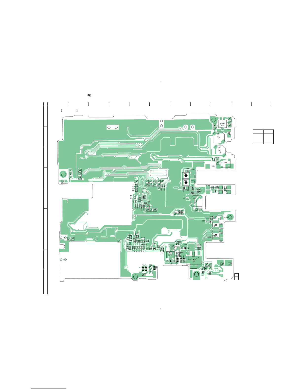
3939
MZ-N10
6-3. Printed Wiring Board – MAIN Board (Side A) – :Uses unleaded solder.
MAIN BOARD (SIDE A)
12
A
B
C
D
E
F
G
H
I
34567891011
1-686-347-
12
(12)
S804
(PROTECT)
S803
(OPEN/CLOSE)
C938
C347
C303
R945
R947
C623
• Semiconductor
Location
Ref. No. Location
D604 H-7
D952 G-7
Q954 H-8
Page 40
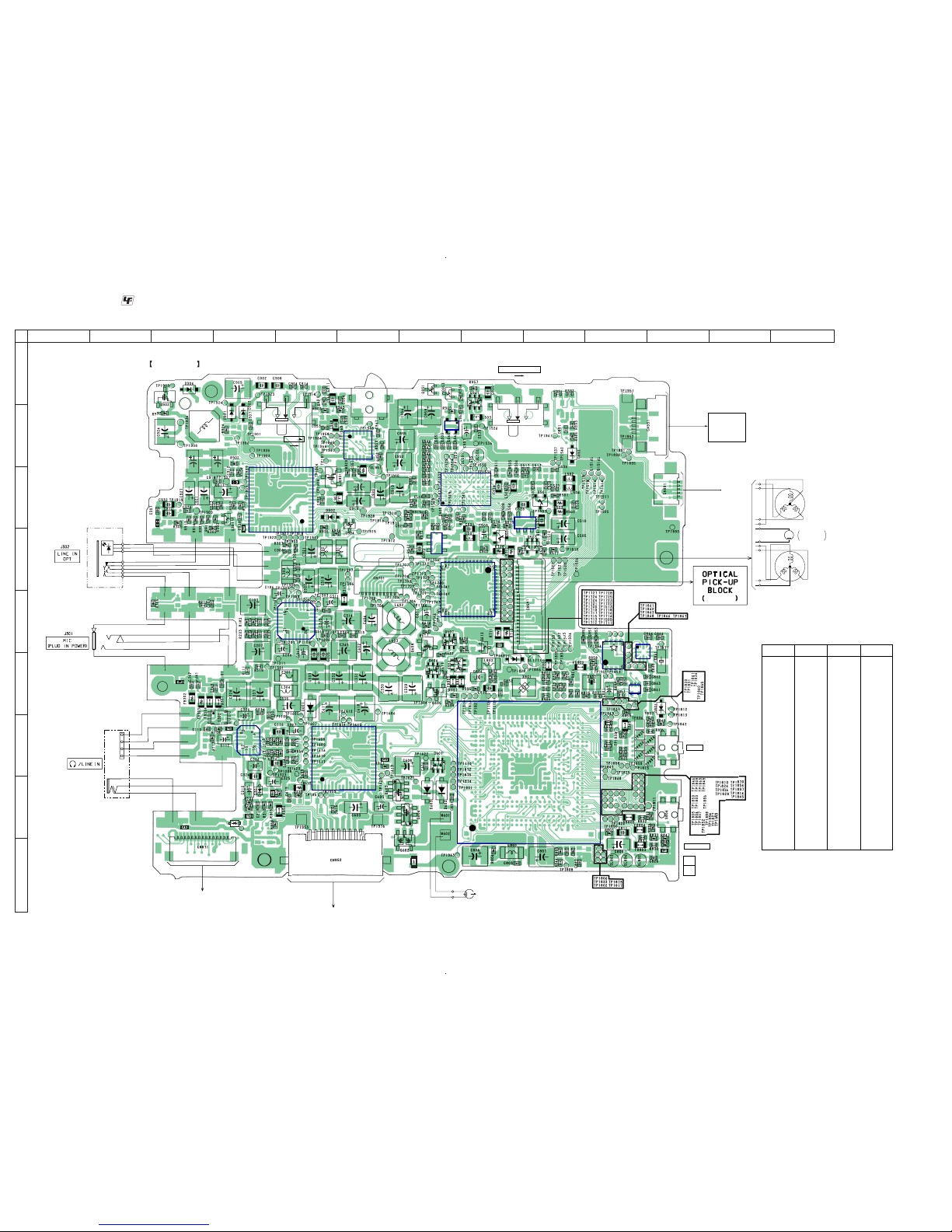
4040
MZ-N10
– MAIN Board (Side B) – :Uses unleaded solder.
IC951
IC901
IC301
IC501
IC952
IC503
IC701
IC601
IC302
IC851
IC861
IC862
IC801
IC502
MAIN BOARD (SIDE B)
(
)
J303
SWITCH
&
LCD MODULE
TO USB CRADLE
OVER WRITE HEAD
S806
END SEARCH
S805
T MARK
(HALF LOCK)
HOLD
OFF ON
ABX-1R
TO
JOG
DIAL
RECHARGEABLE
BATTERY
LIP-3WMB,
3.7V,340mAh,
Li-ion
BUILT IN BATTERY
OFF
ON
1
M
10
U
U
N
VW
N
V
W
M602
(SLED)
M601
(SPINDLE)
M603
OVER WRITE
HEAD UP/DOWN
S801
1-686-347-
12
(12)
C809
C833
R821
R822
TP1857
TP1855
TP1856
C523
C527
C534
TP1508
TP1833
TP1837
TP18444
R841
TP1829
C815
R838
TP1601
D610
RVDD
DTCK
KEY_R
RGND
*
CSP(Chip Size Package)
*
CSP(Chip Size Package)
S951
S802
1
10
C915
C937
C936
L901
C906
C308
C323
C339
C614
R313
R105
R212
R602
R961
R936
TP1204
TP1104
D201
R860
R843
12
A
B
C
D
E
F
G
H
I
34567891011 12 13
D201 H-4
D301 H-4
D302 G-3
D601 F-5
D602 H-7
D603 H-7
D610 F-8
D801 G-11
D892 B-9
D901 B-4
D902 C-5
D903 B-4
D904 A-3
IC301 E-5
IC302 G-4
IC501 C-8
IC502 D-7
IC503 C-9
IC601 G-6
IC701 D-8
IC801 G-9
IC851 F-10
IC861 F-10
IC862 E-10
• Semiconductor
Location
Ref. No. Location
IC901 C-5
IC951 B-6
IC952 B-7
Q301 C-4
Q501 C-9
Q502 D-8
Q503 D-9
Q601 G-7
Q602 I-7
Q603 H-6
Q604 H-7
Q605 F-7
Q606 F-7
Q607 E-7
Q608 F-7
Q612 E-8
Q901 C-5
Q902 A-3
Q904 D-6
Q951 A-7
Q952 F-7
Q953 A-7
Q961 A-8
Ref. No. Location
Page 41
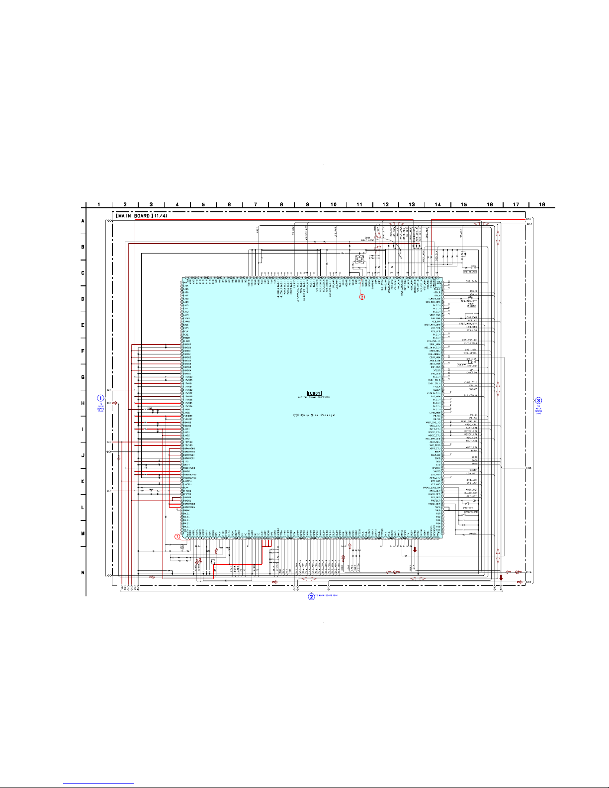
4141
MZ-N10
6-4. Schematic Diagrams – MAIN Board (1/4) – • See page 38 for Waveforms.
C831
C832
L802
C802
C804
C833
R803
C805
R804
C806
TP896
TP897
R849
C808
TP1820
R841
L803
C803 C807
TP1811
R806
X801
C809
C810
R805
FB801
C811
TP1105
TP1205
R807
R809
R808
C812
C813
C814
C817
R813
C818
R816
TP1021
C820
C821
C822
C823
TP1822
TP1869
FB803
FB804
FB805
R830
R831
R832
TP1823
TP1816
TP1817
TP1818
TP1872
TP1873
TP1874
TP1875
R844
R839
C825
SL802
C826
S803
S804
SL804
TP1859
TP1858
TP1854
TP1813
TP1812
TP1815
TP1828
TP1810
TP1824
TP1825
TP1826
TP1827
TP1870
TP809
TP1829
TP1809
TP1897
SL803
S802
TP1801
TP1808
TP1850
TP1807
TP1806
R838
C827
TP1802
TP1803
TP1804
TP1805
TP1849
TP1848
TP1847
S806
S805
R836
R802
C829
TP1844
TP1846
S801
TP1843
TP1842
TP824
TP825
TP826
TP827
TP828
TP1888
TP1889
TP1890
TP1894
TP1896
TP1814
TP1845
TP1886
TP1887
TP1830
TP1831
R843
TP1841
TP1832
TP1833
TP1834
R845
X802
R823
R825
R826
R827
FB802
R828
R829
R821
R822
R824
TP1835
TP1836
TP1837
TP1838
R851
R833
TP1839
TP1840
R856
R850
R859
C819
C801
R840
R858
R857
R834
R835
R837
R848
R847
C834
C815
R811
R819
R820
R817
R814R815
R818
D801
IC801
0.1 F
0.1 F
0.1 B
10 6.3V
0.1 F
10
10 6.3V
10
47 6.3V
0
1000p B
0
0.1F47
6.3V
0
22.5792MHz
1p
Ck
1p
Ck
0
0
1
B
10k
100k
10k
1
B
0.01
B
0.47
B
1B
1k
0.1
C830
0.1
B
220
0.01 B
0.022 B
0.01 B
0.022 B
0
0
0
0
0
0
0
0
0.01 B
0.01 B
2.2k
0.1 B
0
1k
4700p
B
0
0
48MHz
01M
2.2k
4.7k
0
22
22
47k
220k
470k
0
0
0
10k
220k
0.1
B
4.7 6.3V
1M
47k
47k
4.7k
4.7k
100k
220k
100k
R860
2.2M
0.022
B
470p B
220k
2.2k
2.2k
2.2M
1M
2.2k1k
MA728-TX
CXD2678-202GA
*
(Page 42)
(Page 44)
(Page 43)
Page 42
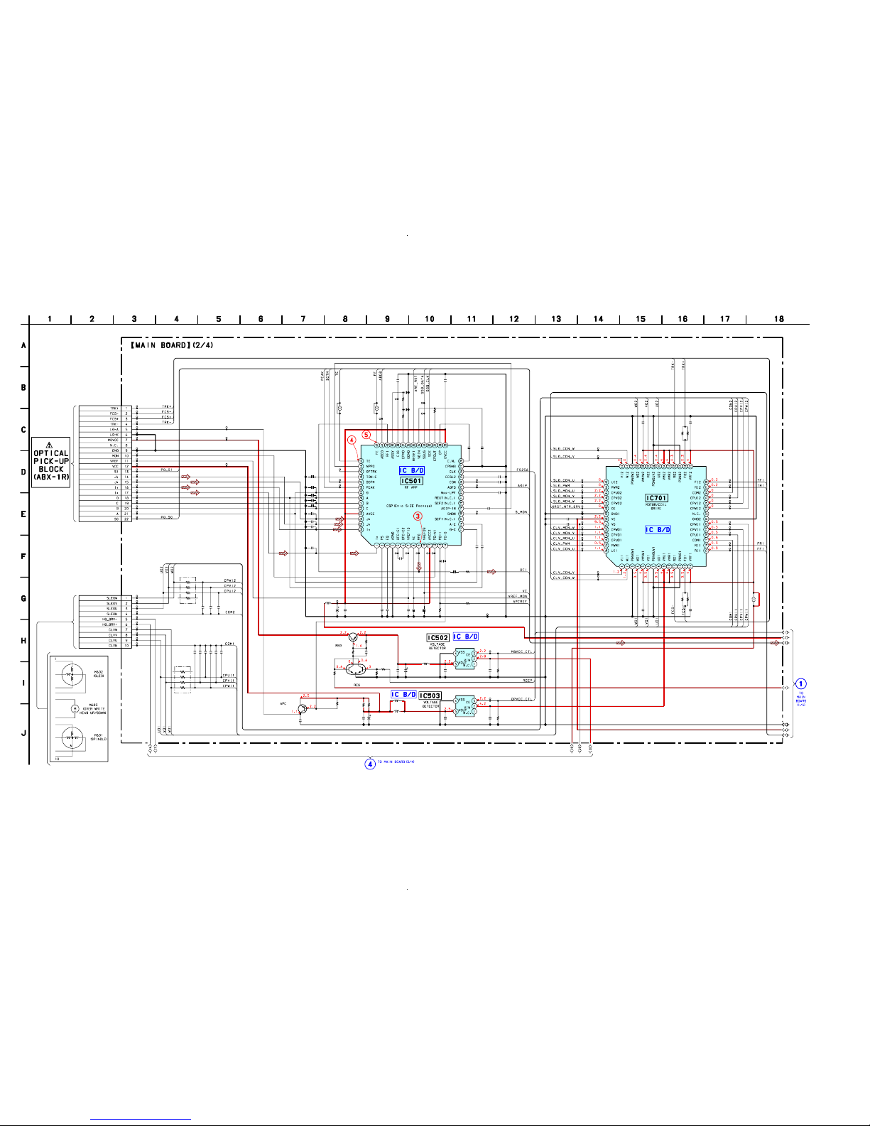
4242
MZ-N10
– MAIN Board (2/4) – • See page 38 for Waveforms. • See page 45, 46 for IC Block Diagrams.
TP1502
TP1503
TP1504
TP1506
TP505
TP507
TP501
TP510
TP1511
TP1510TP512
TP1513
TP1514
TP1515
TP1516
TP1517
TP1518
TP1519
TP1520
TP1521
TP1522
TP1507
TP1509
CN501
SL501
TP1501
SL502
TP1535
C513
TP1539
R504
C518
R505
TP523
TP1538
C524
R511
C526 C535
TP1537
TP1540
TP1541
C536
C537
C538
C533
C534C527
R509
C540
C523
TP1505
TP1530
TP1529
TP1528
TP1527
C514
IC501
TP1523
TP1524
TP1525
C506
C544
C543
C545
C546
C547
C549
C507
C509
C511 C512 C519 C520 C522 R507 R508
TP1536
R514
C554
R515
R517
R518
R516
C502
C504
C501
R501
C505
C508
R502 R503
C510 C528 C552
R513
TP1512
C503 R512
TP1500
R711
TP1711
TP1712
TP1713
TP1714
TP1715
TP1716
TP1717
TP1718
TP1719
TP1720
TP1721
TP1722
TP1723
TP1724
TP1725
TP1726
C716
CN701
RB701
C701
C702 C703
TP1727
TP1728
RB702
TP1701
TP1702
TP1703
TP1704
TP1705
TP1706
TP1707
TP1708
TP1709
TP1710
TP1747
TP1736
TP1737
TP1739
TP1740
TP1741
TP1742
TP1743
TP1744
TP1746
SL1711
R712
R714
C721
C720
C712
C711
C710
C709
C708
C707
C715
C719
C718
TP1526
L502
L504
C517
R713
Q503
Q502
IC502
IC503
Q501
IC701
C548
C551
L501
U
V
W
V
U
W
N
L503
22P
0.022
B
10k
0.01
B
10k
1
B
0
0.047B1
B
0.1 B
0.022 B
0.022 B
0.01 B
4700pB4700p
B
0
4700p
B
2200p
B2200p
B
SN761058ZQLR
0.01
B
22p CH
22p CH
22p CH
22p CH
22p CH
22p CH
10
6.3V
0.1
B
10pCH10pCH0.1B0.1B0.1B10k
0.5%
1k
47k
0.1
B10k
10k
47k
100k
0.1
B
4.7
6.3V
1
B
100k
10
6.3V
0.1
11
10
6.3V
1
B
1
B
2.2M
1
B
2.2M
22
0.1 F
10P/S
2.2k
0.022
B
0.022B0.022
B
10k
22
22
0.1
F
0.1
F
0.022
B
0.022
B
0.022
B
0.01
B
0.01
B
0.01
B
0.1 F
0.1
F
0.1
F
0.01
B
22
XP1501-TXE
2SA1745-6.7-TL
XC62HR2202MR
XC62HR2502MR
2SA1577-T106-QR
SC111258EPR2
22p
CH
22p
CH
10µH
10µH
10µH
10µH
*
(Page 43 )
(Page 41)
Page 43
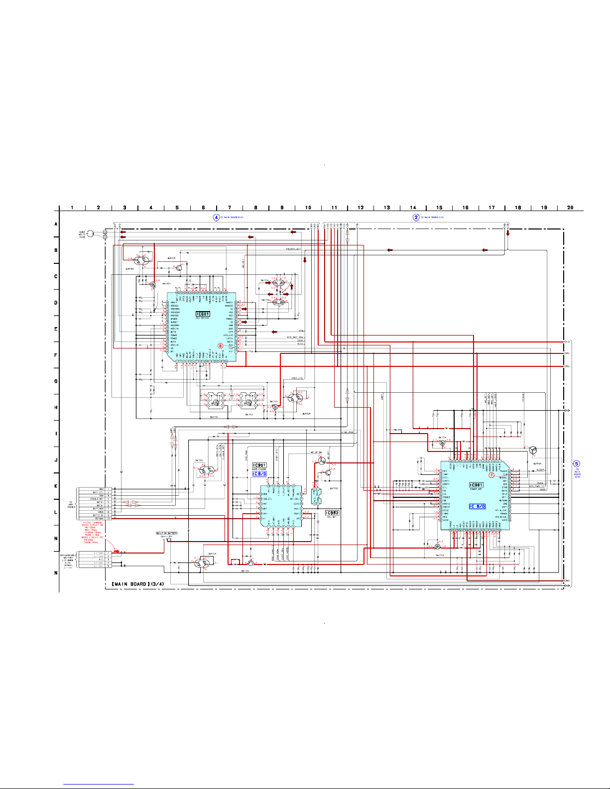
4343
MZ-N10
– MAIN Board (3/4) – • See page 38 for Waveforms. • See page 47, 48 for IC Block Diagrams.
W601
W602
R622
R625
R626
R614
R617
C611
D610
C627
TP1607
TP1602
TP1617
TP1612
TP1614
TP1615
TP1606
TP1604
R630
TP1601
C604
C602
C617
C618
TP1608
TP1609
TP1623
TP1616
TP1610
TP602
R610
R612
C622
C619
C609
C610
C621
R627
D604
C605
C626
C612
TP1618
TP1619
TP1620
TP1621
TP1622
TP601
C606
C608
C603
R613
R618
R974
FB953
TP1957
TP1959
TP971
TP975
TP976
TP977
TP978
TP979
TP980
TP972
TP973
TP974
CN952
R956
FB954 FB952
TP1953
FB955
TP1976
TP1952
TP952
TP1951
TP956
R957
C960
R963
C959
TP1968
C954
C966
C961
C951
C968
R951
R953
R955
R954
TP1969
TP1958
TP1965
TP1966
TP1967
C953
C952 C955 C956 C958 C957
R959
R958
TP953
TP954
TP955
TP960
SL951
R952
C967
TP1961
TP1963
R964
C962
R960
C916
TP1928TP927
TP987
TP908
C919 C920
C925
R929
TP1904
TP1906
TP1929
C922
R934
R905
R931
R907 R912 R915
R917
TP1915
TP1910
TP1911
TP1912
TP1913
R918
TP1916
TP1917
TP1918
TP1919
TP1920
TP1921
TP1922
C932
C910
R903
TP1901
C902
C909
C907
TP910
TP911
TP1923
TP1924
TP1902
C904
C906
R902
C912
R904
R932
TP1935 TP901
C917
C918
C921
C923 C924
TP1903
TP926
TP1927
TP1905
TP902
TP903
TP1907
TP1908
TP904
TP906
TP905
TP1936
TP1909
TP1914
TP909
R908
R909
R911
R914
R919
R921
R923
C929
C927
C926
IC901
C625
R995
R994
R997
C615
CN951
C933
R935
L601
L605L604
L602 L603
R603
R606
R620
R621
D901
D904
D903
Q953
IC952
Q951
IC951
Q952
R975
R901
Q902
R926
L902
C911
C914
C908
Q904
D902
L904
L903
Q901
D601
Q608
Q607
IC601
D603
D602
Q602
Q601
Q612
Q603
Q604
Q606
Q954 D952
Q961
R619
Q605
S951
100k
100k
220k
2.2M
100k
4.7
10V
MA728-TX
0.01
B
0
10 6.3V
10 6.3V
22 10V
22 10V
2.2k
1
1B
0.01
B
0.1 F
4700p
C623
0.1
47
6.3V
1k
MA22D2800LS0
10
6.3V
10
6.3V
0.1
C614
0.1
B
0.1
F
47
6.3V
10
10V
2.2M
1k
0
0
10P
22k
000
100k
0.22
B
2.2k
0.1
B
4700p B
1B
4.7 B
4.7 B
1B
2.2
1
100
R961
0
10k
0.1
B
22
10V2210V2210V2210V
0.1
F
220
0.5%
100
0.5%
0.022
0.1
B
47k
0.1 B
47k
10
6.3V
C915
10
6.3V
47
6.3V106.3V
4700p
B
220k
R936
4.7k
0.1
B
10k
10k
0.5%
0
470k 100k 220k
470k
470k
1B
1B
1k
1
B
10
16V
C936
10
16V
C937
10
16V
C938
10
16V
0.1
0.1
470p
B
1M
0.047
B
1k
220k
10
6.3V
0.1
F
10
6.3V
0.1F47
4V
47k
0.5%
100k
0.5%
47k
47k
47k
47k
100k
0.5%
0.01
B10
6.3V
0.1
F
SC901580EPR2
0.1
B
220k
2.2M
2.2M
0.01
B
5P/S
0.1
470k
10
10
10
R602
47k
10
MA729-TX
MA729-TX
MA729-TX
2SC4738F-Y/GR
(TPL3)
XC6ICN3002NR
UN9113J-(TX).SO
SC901582EPR2
XP4314-TX
0
1M
XP152A12C0MR
22k
0.01
B
1000p
1
UN9214J-(TX).SO
MA111-TX
XP152A12C0MR
MA22D2800LS0
XP151A13AOMR
XP4314-TX
SC901581EPR2
MA2YD1700LS0
MA2YD1700LS0
CPH5614
MCH6616-TL-E
2SD2216J-QR(TX).SO
RTQ045N03
RTQ035P02
XP4314-TX
FZT968TA MA22D2800LS0
XP4314-TX
220
SI2302DS-T1
L1-SW
0µH
10µH
10µH
10µH10µH
L901
270µH
330µH
10µH
220µH
(Page 42)
(Page 41)
(Page 44)
Page 44
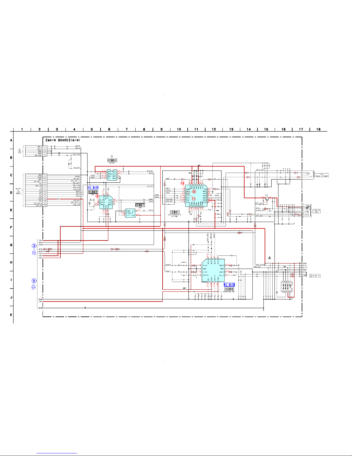
4444
MZ-N10
– MAIN Board (4/4) – • See page 38 for Waveforms. • See page 45, 47 for IC Block Diagrams.
TP881
TP882
TP883
TP884
TP1891
TP1892
TP1893
TP1895
R893
R892
R891
C891
R871
CN891
CN871
TP895
R853
C851
TP1857
TP1856
TP1855
R852
TP1851
TP1852
C864
TP1861
TP1871
TP871
C866
TP1867
TP1866
C862
C863
C865
TP1868
TP1862
TP1863
TP1865
C861
L301
C315
C316
C314
C313
C312
C311
TP1309
TP1302
TP1303
TP1304
TP1305
TP1306
TP1307
TP1308
R308
R309
TP1206
C205
C105
TP1106
C317
C344
C345
TP1313
C318
C320
TP1207
C319
L303
C321
C322
C206
C207
TP1301
R319
C107
C106
TP1107
TP302
TP101
TP201
TP301
R301
R111
R211
TP303
C101
C201
C103
C203
C301
C202
C102
R104
R103R203
R204
TP309
TP202
TP102
TP308
TP304
TP305
TP306
TP307
TP310
C306
R307
R303
R302
R306
R101
R201
C104 C204
R202
R102
TP1311
R312
R315
R313
R310
C325
C326
C324
C212
C215
C214
R208
TP1208
C216
C116
TP1108 R108
R109
C114
C115
C113
C327
L304
R320
C329
C330 C331 C332 C333
C334
C335 C336 C337
C328
C211
TP1204
TP1104
C111
C112
R206
R106
C210
C110
R205
R105
R212
R112
C342
R321
FB301
FB303
FB304
J303
TP320
L302
R317
TP315
TP316
TP317
TP318
TP319
TP103
TP203
R209
TP1323
R305
R894
C310
D301
IC302
C340
C341
C343
FB302
C307 C308
Q301
IC301
IC862
IC851
D302
D892
R304
J301
X861
IC861
C213
F301
J302
0
0
0
4700p
B
0
5P/S
15P/S
100k
0.1
F
100k
0.1
B
2p
CH
0.1
B
0.1
B
0.1
B
0.1
B
2.2
6.3V
0.1
B
47 6.3V
0.1 B
0.1 B
10 6.3V
1k
1k
1
B
1
B
2.2
6.3V
0.1 B
47 6.3V
47 6.3V
10 6.3V
0.1 B
22 6.3V
0.1 B
4.7
6.3V47
4V
0
47
4V
4.7
6.3V
100
0
0
2200p
C303
1000p
C323
2200p
C347
1000p
1000p 1000p
B
2200p
B
1000p
B
1000p
B
10
6.3V
0.1
B
0.1 B
10k
0.5%
22k
0.5%
22k
0.5%
10k
0.5%
0.1
B
1k
100k
10k
100
47k 0.5%
47k
0.5%
100pCH100p
CH
22k
0.5%
22k
0.5%
100k
10k
0.5%
220k
220k
0.5%
4.7
6.3V
2.2 6.3V
1B
2.2 6.3V
2200p B
4700p B
10k 0.5%1B
1B
10k 0.5%
10k 0.5%
4700p B
2200p B
470p B
22 4V
0
47
4V
474V474V474V47
4V
0.01
B
22
6.3V224V476.3V
47
6.3V
220
2.5V
220 2.5V
2.2 6.3V
22
22
0.01
B
0.01
B
10k
10k
1
1
1000p
1000p
1M
0
0
0
10k 0.5%
100
1M
0.1
B
M
A2S111-TX
AN17020A-VB
C339
1000p
1000p
0.01
B
100
2SA2018TL
AK5356VN-L
R2061K01-E2
AK6510CL-L
DF8A6.8FK(TE85R)
MA728-TX
100
32.768KHz
TC7SZ126AFE
470p
B
0.25A/125V
TO
(Page 41)
(Page 43)
D201
MA2511I-TX
Page 45
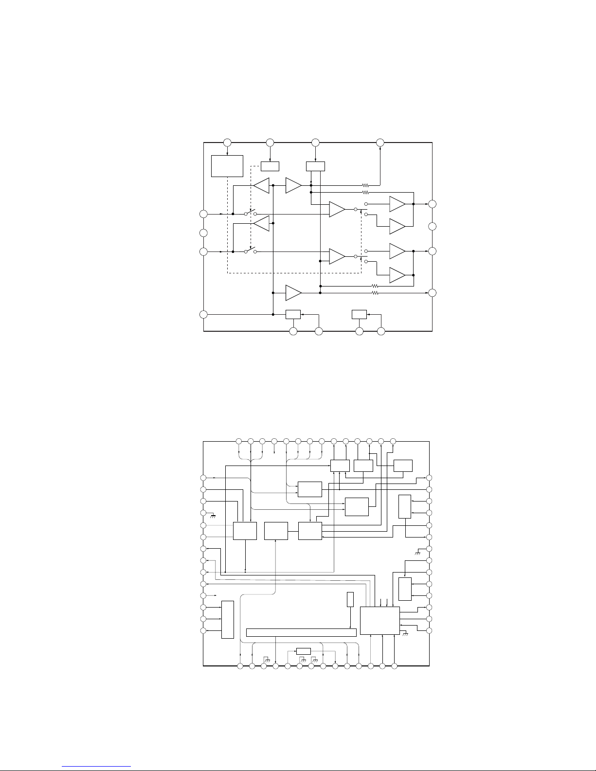
45
MZ-N10
IC501 SN761058ZQLR
1
IX
2
PS
3
EQ
4
A GND
5
OFC-C1
6
OFC-C2
7
VREF10
8
VC
9
RFO
10
VREF09
11
AVCC2 AVCC2
AVCC
AVCC2
12
PD-NI
13
PD-I
14
14-O
D-C
A-C
AGND
SMPN
ADIP-IN
AGND
AGND
WPP-LPF
ADFG
CON
CCSL2
CLK
CPGND
NC
56 55 54 53 52 51 50 49 48
PEAK/
BOTM
47 46 45
42
FE
41
ABCD
40
RFI
39
ASSY
37
EFMO
DGND
RESET
34
VGIN
33
SBUS
32
SCK
CPOUT
CP
DVCC
IY
JYJXAVCC
AVCC
C
B
A
D
PEAK
BOTM
TON-C
OFTRK
PPON
TE
44 43
15 16 17 18 19 20 21 22 23 24 25 26 27 28
31
30
29
35
36
38
CIG
ABCD
T-ON
EFM
COMP.
SERIAL
I/F
POWER
SUPPLY
SIGNAL MONITOR
OFTRK
FE
TPP/WPPRF
A+B+C+D
I+J
NPP
TON
CSL
AW+DW
TONE PEAK
TON BOTM
ADIPTETWP-P
PK/BTMAWCSLO
VREF
A-C
D-C
OFTTH
PD-NI
ADIP-BPF
TEMP
ADIP
APC
TE
• IC Block Diagrams
1
2
5
3
4
6 7 8
13141516
12
11
10
9
+
–
+
–
MUTE
RF1 RF2
BEEP
HEADPHONE
/LINE
SWITCH
GA-R
BEEP
MUTE
HP/L
R-IN
GND
L-IN
RIP-F1
CR
VCC1
RIP-F2
VCC2
ROUT
GND
LOUT
GA-L
IC302 AN17020A-VB
Page 46
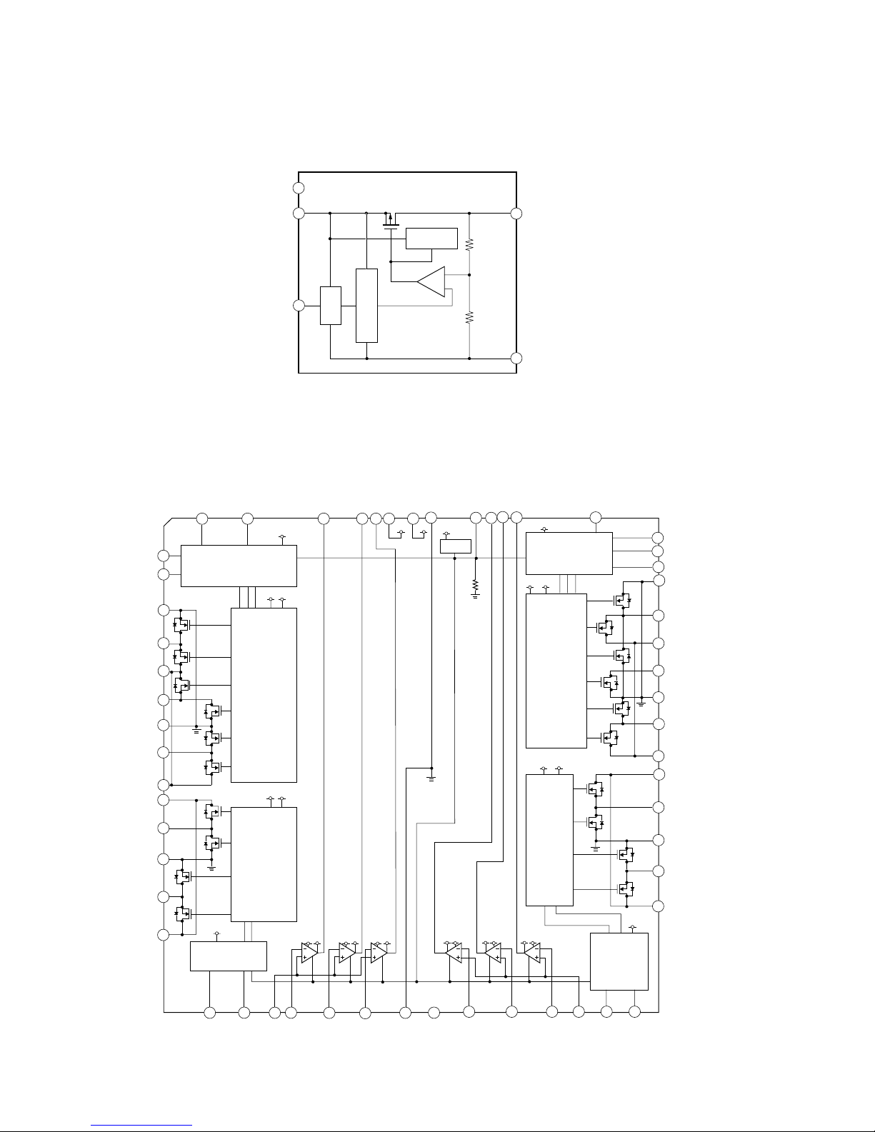
46
MZ-N10
IC502 XC62HR2202MR
IC503 XC62HR2502MR
NC
VIN
CE
VSS
VOUT
CURRENT
RESTRICTION
OUTPUT
CONTROL
4
5
1
2
+
–
THE SOURCE OF
CONSTANT VOLTAGE
3
IC701 SC111258EPR2
14
13
56 55
CPWI2
CPVI2
CPUI2
COM2
RI2
FI2
UI1
PWM1
CPUO1
CPWO1VGVC
36
37
38
39
40
41
52 51 50
49
48
47
46
45
44
43
42
23
24
25
12
11
10
9
8
7
6
5
4
3
2
1
GND1
OE
OE
OE
CPWO2
CPVO2
CPUO2
PWM2
UI2
VI2
WI2
PGNDW2
WO2
VMVW2
VO2
PGNDUV2
29
30
31
32
33
34
35
UO2
VMU2
VMR2
RO2
PGND2
FO2
VMF2
VI1
WI1
PGNDW1
WO1
WMVW1
VO1
PGNDUV1
UO1
VMU1
VMR1
RO1
PGND1
FO1
VMF1
19
18
17
16
15
FI1
RI1
COM1
CPUI1
CPVI1
22
21
20
CPWI1
GND2
NC
BIAS
VC
ROE
VC
3Phase
control
ch1
3Phase
control
ch2
3Phase
Pre driver
ch1
H-BRIDGE
PRE
DRIVER
CH1
H-BRIDGE
CONTROL
CH1
VC
VCVGVCVGVC VC
OE
VG VGVCVG
VC
VG
GND
VG
VC
VG
VC
VG
VC
VG
VC
VC
VC
U
VW
UVW
H-BRIDGE
CONTROL
CH2
VCVG
3Phase
Pre driver
ch2
H-BRIDGE
PRE
DRIVER
CH2
26
27 28
CPVO1
5354
Page 47
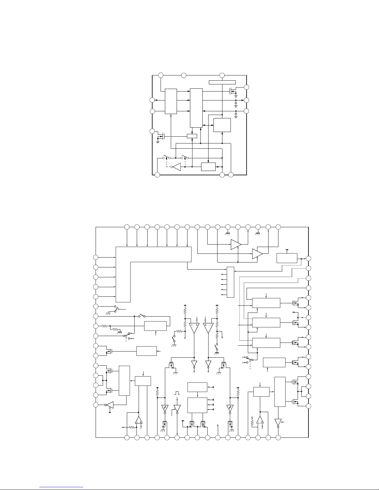
47
MZ-N10
IC862 R2061K01-E2
SIO
SCLK
/VDCC
OSCIN
OSCOUT
CIN
VSS
CE
SW2
VOLTAGE
DETECTOR
VSB
SW1
4
DELAY
3
VCC
5
VOLTAGE REFERENCE
BATTERY
VOLTAGE
MONITOR
REAL
TIME
CLOCK
LEVEL
SHIFTER
VDD
6
1011
12
7
8
9
1
2
/INTR
IC901 SC901580EPR2
1
FFCLR1
2
XWK4
3
XWK3
4
XWK2
5
XWK1
6
VRMC
12
VO1
13
L1
14
L1
15
PGND11
16
17
VC1G
RF1
VMODE
REF2
18
INM119DTC1
20
CRST121XRST1
22
CIL
23VG24LG25
PGND3
VB
26
XRST227CRST2
28
DTC229INM2
30 31
RF2
32
VC2G
7
LVB
8
HVB
9
VSTB
10
VC1
11
VCO1
48
VREF
47
REGC3
46
REGC2
45
REGC1
44
REGI1
43
REGO1
37
VCO2
36
VO2
35
L2
34
L2
33
PGND2
42
VC2
41
REGO2
40
REGI3
39
REGO3
38
CVIN
64
SLEEP63CLK62SEQSEL61WDT60SCK59STRB58DATA57HPI256HPI155MUTEON54GND53VHP152HP151PGND450HP249VHP2
PWM
START-UP
SET-UP
DC/DC
CONVERTOR
SET-UP
PRE DRIVER
SERIES PASS
REGULATOR1
CONTROL
BANDGAP
REFERENCE
REF DAC
SERIES PASS
REGULATOR2
SERIES PASS
REGULATOR3
POWER
AWITCH 2
POWER
AWITCH 1
LVB
DRIVER
REF1
REF2
REF3
REF3
REF4
REF5
XRST2
XRST2
FFCLR
XRST1
XRST1
REF4
REF5
VC2
VC
(HP AMP)
AMP1
AM2
VC2
VC2
VF2VF1
VG
XRST2
XRST2XRST1
XRST1
SEQSEL
VG
VG
XRST1
VB
VB
VG
VB
VC
VG
VG
VC
VG
REF2
VF2
PWM
SET-UP
PRE DRIVER
XRST1
VC
VC
VF2
REF1
REF2
(VCC)
(VCC)
Page 48
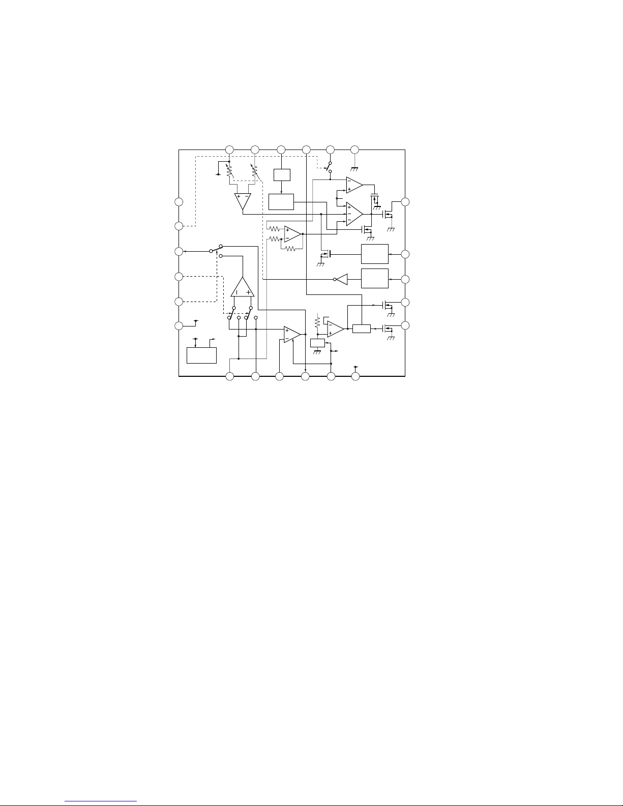
48
MZ-N10
IC951 SC901582EPR2
1
2
3
4
5
6
7 8 9 10 11 12
18
17
16
15
14
24 23 22 21 20 19
DELAY
VCR
TIME
DIVIDER
OSC
LOGIC
SIGNAL
RECEIVER
VOLTAGE
REFERENCE
LOGIC
SIGNAL
RECEIVER
VO
VREF
NSW1
VI2
VI
VG
N3
N2
N1
VI
CAP_C_LIM
VI2DET
A/D
I_SEL
AD_SEL
VI2
RF1
I_CTL1
I_CTL2
WK_DET
PWR_WAKE
VREF
VREF
SW4
SW5
SW6
NSW4
NSW3
BATT
SEL
VO
VBAT
IN2-
OUT2
BAT_SEL
VG
VI
IN1
WDT
PWT
CHG_CTL
GND
Page 49
49
MZ-N10
6-5. IC Pin Function Description
• IC801 CXD2678-202GA (SYSTEM CONTROLLER, DIGITAL SIGNALPROCESSOR)
Pin No.
1
2
3
4
5
6
7
8
9
10
11
12
13
14
15
16
17
18
19
20
21
22
23
24
25
26
27
28
29
30
31
32
33
34
35
36
37
38
39
40
41
42
43
44
45
46
47
48
49
50
I/O
I
O
O
O
O
O
O
I
I
I
O
I
O
I
I
I
I
I
I
O
I
I
I
I
I
I
I
I
O
O
O
O
O
O
O
O
O
O
O
I
I
I
O
O
I
I
I
O
I
O
Pin Name
OSCI
OSCO
VREFL
AOUTL
AOUTR
VREFR
ASYO
ASYI
BIAS
RFI
PCO
FILI
FILO
CLTV
PEAK
BOTM
ABCD
FE
VC
ADIO
ADRB
SE
TE
AUX1
ADRT
DCHG
APC
ADFG
APCREF
TRDR
TFDR
FFDR
FRDR
FS4
SFDR
SPRD
SPFD
SPDV
SPDW
SPCU
SPCV
SPCW
SLDV
SLDW
SLCU
SLCV
SLCW
SRDR
DIN
DADT
Description
Resonator connection terminal for the system clock (22.5792MHz)
Resonator connection terminal for the system clock (22.5792MHz)
Reference voltage terminal connected to the capacitor (for the built-in D/A converter L-CH)
Built-in D/A converter L-CH signal output
Built-in D/A converter R-CH signal output
Reference voltage terminal connected to the capacitor (for the built-in D/A converter R-CH)
Playback EFM duplex signal output
Playback EFM comparator slice level input
Bias current input terminal for the playback EFM comparator
Playback EFM RF signal input from the RF amplifier
Phase comparison output terminal for the playback EFM system master PLL
Filter input terminal for the playback EFM system master PLL
Filter output terminal for the playback EFM system master PLL
Internal VCO control voltage input terminal for the playback EFM system master PLL
Peak hold signal input of the light amount signal (RF/ABCD) from the RF amplifier
Bottom hold signal input of the light amount signal (RF/ABCD) from the RF amplifier
Light amount signal (ABCD) input from the RF amplifier
Focus error signal input from the RF amplifier
Middle point voltage input from the RF amplifier
Monitor output terminal of A/D converter input signal Not used (open)
The lower limit voltage of A/D converter input terminal (connected to the ground)
Sled error signal input from the RF amplifier
Tracking error signal input from the RF amplifier
Auxiliary A/D input (fixed at “H” in this set)
The upper limit voltage of A/D converter input terminal (fixed at “H” in this set)
Connecting terminal with the analog power supply of low impedance (fixed at “H” in this set)
Error signal input for the laser automatic power control (fixed at “H” in this set)
ADIP duplex FM signal (22.05±1kHz) input from the RF amplifier
Reference PWM signal output for the laser automatic power control to the RF amplifier
Tracking servo drive PWM signal output (–) to the coil driver
Tracking servo drive PWM signal output (+) to the coil driver
Focus servo drive PWM signal output (+) to the coil driver
Focus servo drive PWM signal output (–) to the coil driver
176.4kHz clock signal output
Sled servo drive PWM signal output to the motor driver
Spindle motor drive control signal output (U) to the motor driver
Spindle servo drive PWM signal output to the motor driver
Spindle motor drive control signal output (V) to the motor driver
Spindle motor drive control signal output (W) to the motor driver
Spindle motor drive comparison signal input (U) from the motor driver
Spindle motor drive comparison signal input (V) from the motor driver
Spindle motor drive comparison signal input (W) from the motor driver
Sled motor drive control signal output (V) to the motor driver
Sled motor drive control signal output (W) to the motor driver
Sled motor drive comparison signal input (U) from the motor driver
Sled motor drive comparison signal input (V) from the motor driver
Sled motor drive comparison signal input (W) from the motor driver
Sled motor drive control signal output (U) to the motor driver
Digital audio signal input
Audio data output terminal Not used (open)
Page 50
50
MZ-N10
Pin No.
51
52
53
54
55
56
57
58
59
60
61
62, 63
64 to 66
67
68
69
70
71
72
73
74
75
76
77
78 to 85
86
87
88
89
90
91
92
93
94
95
96
97
98
99
100
101
102
103
104
105
106
107
108
I/O
I
O
O
O
O
I
I
I
I
—
O
—
O
O
O
O
O
O
I
I/O
O
O
O
O
—
—
—
I
I
I
I
I
I
O
O
O
O
O
I
I
O
O
I
O
O
O
O
O
Pin Name
ADDT
KRCK
XBCK
FS256
NC
NC
LRCKI
XBCKI
DATAI
NC
TSTDR1
NC
MNT0 to 2
MNT3
SENS
TX
RECP
EFMO
FMCK
OFTRK
XSKH
XSKL
DCLSOUTL
DCLSOUTR
TD0 to 7
TREQ
TAC K
PAUSE_KEY
PROTECT
OPT_DET
XJACK_DET
XMIC_DET
OPEN_CLOSE_SW
XCS_ADC
XPD_ADC
CHG_CTL
LCD_RST
XMUTE
XPATCH
SI0
SO0
SCK0
XGUM_ON
BEEP
XOPT_CTL
XHP_STBY
AOUT_SEL
REC_OPR_LED
Description
Data input from the external A/D converter
L/R sampling clock (44.1KHz) output to the external A/D converter
Bit clock (2.8224MHz) output to the external A/D converter
11.2896MHz clock output
Filter cutoff control signal output Not used (open)
Clock input from the external VCO Not used (open)
Input terminal for the PCM data I/F/ ATRAC data I/F Not used (open)
Input terminal for the PCM data I/F/ ATRAC data I/F Not used (open)
Input terminal for the PCM data I/F/ ATRAC data I/F Not used (open)
Not used (open)
Not used (open)
Not used (open)
DSP monitor (0) to (2) output terminal Not used (open)
DSP monitor (3) output terminal
DSP internal status (DSP SENS monitor) signal output terminal Not used (open)
Record data output enable signal output Not used (open)
Laser power changeover signal output
EFM encode data output for the record to the REC driver
FMCK signal input Not used (connected to the ground)
Tracking signal input/output Not used (open)
L circuit signal output Not used (open)
K-SHOCK circuit signal output Not used (open)
PWM modulator signal output for the D class headphone amplifier Not used (open)
PWM modulator signal output for the D class headphone amplifier Not used (open)
TigerI/F data 0 to 7 terminal Not used (open)
TigerI/F REQUEST terminal Not used (connected to the ground)
TigerI/F ACK terminal Not used (connected to the ground)
Pause key detection input terminal from the switch & liquid crystal display module
Detection signal input terminal of the record check claw from the protect detection switch “H”: protect
DIN plug detection signal input “H”: DIN plug detect
LINE IN plug detection signal input “L”: LINE or OPT plug detect
Microphone plug detection signal input “L”: microphone plug detect
Open/close detection switch of the upper panel input terminal “L”: when upper panel close
Chip select signal output to the A/D converter
Power supply control signal output to the A/D converter
Charge ON/OFF control signal output Not used (open)
Reset control signal output to the liquid crystal display module
Analog muting control signal output to the headphone amplifier “L”: muting ON
Patch function detection terminal “L”: patch function (fixed at “L” in this set)
Serial data input from the real time clock, A/D converter, nonvolatile memory and liquid crystal display module
Serial data output to the real time clock, A/D converter, nonvolatile memory, liquid crystal display module,
power control and REC driver
Serial clock output to the real time clock, A/D converter, nonvolatile memory, liquid crystal display module,
power control and REC driver
Rechargeable battery detection switch input terminal “L”: rechargeable battery in detect Not used (open)
Beep sound control signal output to the headphone amplifier
Power supply ON/OFF control signal output for the DIN PD drive
Power supply control signal output to the headphone amplifier Not used (open)
HP/LINE changeover signal output to the headphone amplifier
LED ON/OFF control signal output for the REC display
Page 51
51
MZ-N10
Pin No.
109
110
111
112
113
114, 115
116
117
118
119, 120
121
122
123
124
125
126
127
128
129
130
131
132
133
134
135
136
137
138
139, 140
141
142
143
144
145
146
147
148
149
150
151
152
153
154, 155
156
157
158
159
160
161
162, 163
I/O
O
O
O
O
O
O
O
O
O
O
I
O
O
O
O
O
O
O
I
O
I
I
I
O
O
I
I
O
O
O
O
O
O
O
O
O
O
O
O
I
I
I
O
I/O
O
I
I
I
I
I
Pin Name
MDVCC_CTL
OPVCC_CTL
BATT_CTL
VREC_CTL
XRST_CHG_IC
PD_S0, 1
LINK_MON
NC
NC
NC
SLD_MON
VLON(NC)
SLEEP
FFCLR
CHGI_CTL1
CHGI_CTL2
NC
CHG_LED
XTEST
XRF_RST
XEXT_PWR
XHOLD_SW
COUT_MON
CHG_ADSEL
CHGI_SEL
XDC_IN
SPDL_MON
XCS_PWR_IC
NC
XCS_LCD
LCD_STB
XRST_MTR_DRV
XCS_NV
CHG_PWM
VREC_PWM
NC
NC
NC
XCS_REC_DRV
T_MARK _SW
JOG_A
JOG_B
NC
SSB_DATA
SSB_CLK
VBUS_DET
VB_MON
CHG_MON
VREF_MON
SET_KEY_1, 2
Description
Power supply control signal output for the OP modulation
Power supply control signal output for the OP laser
Control signal output for the voltage step up circuit in the external battery case
VREC voltage control signal output
Reset signal output to the battery charge control IC
PD IC mode changeover signal output to the optical pick up
Linking area monitor signal output Not used (open)
Plunger control signal output Not used (open)
Ground changeover switch control signal output Not used (open)
Not used (open)
Sled servo monitor signal input
Not used (open)
System sleep control signal output to the power control
Input latch output for the start switching to the power control
Charge current limit ON/OFF control signal output at the time of adaptor use
Charge current limit value changeover control signal output at the time of adaptor use Not used (open)
Orange LED ON/OFF control signal output Not used (open)
LED ON/OFF control signal output for CHG (charge display)
Ter minal for the test mode setting (normally open) “L”: test mode
Reset control signal output to the RF amplifier “L”: reset
External power supply (AC adaptor/charging stand) detection signal input Not used (open)
HOLD switch input terminal “L”: hold ON
Traverse count measurement monitor input
A/D terminal of the battery charge contro IC output selection signal output
Charge/discharge changeover control signal output for the current sense amplifier
DC plug detection signal input Not used (open)
Spindle servo monitor signal input
Chip select signal output to the power control
Control signal output for the D class headphone amplifier Not used (open)
Chip select signal output to the liquid crystal display module
Strobe signal output to the liquid crystal display module
Reset control signal output to the motor driver “L”: reset
Chip select signal output to the nonvolatile memory
Output voltage control signal output to the battery charge control
PWM signal output for the power supply voltage control to the REC driver Not used (open)
PWM signal output for the laser power supply voltage control to the power control Not used (open)
Muting control signal to the headphone amplifier (NJM type made by JRC) Not used (open)
Power supply control signal output for the D class headphone amplifier Not used (open)
Chip select signal output to the REC driver
T MARK (track mark) switch input terminal “L”: track mark detection
Jog dial pulse input from the switch & liquid crystal display module
Jog dial pulse input from the switch & liquid crystal display module
Not used (open)
SSB data input/output with the RF amplifier
SSB clock output to the RF amplifier
USB power supply voltage detection terminal
Voltage monitor input terminal (A/D input) of the UNREG power supply
Decrement of voltage detection and charge/discharge current monitor input from the battery charge control
Reference voltage monitor input (A/D input) from the RF amplifier
Key input (A/D input) from the switch & liquid crystal display module
Page 52
52
MZ-N10
Pin No.
164
165
166
167
168
169
170
171
172
173
174
175
176
177
178
179
180
181
182
183
184
185
186
187
188
189
190
191
192
193
194
195, 196
197
198
199
200
201
202 to 204
205, 206
207
208
209
210
211
212
213
214, 215
216 to 231
232 to 245
246
I/O
I
I
I
I
I
I
I
I
I
I
I/O
I/O
I/O
O
O
I
O
I
O
I/O
I
O
I/O
O
O
O
I
I
I
I
I
O
I
O
O
O
O
O
O
I
I
I
I
O
I
I
I
—
—
—
Pin Name
CRADLE_DET
HIDC_MON
WK_DET
BATT_MON
HALF_LOCK_SW
RMC_KEY
JOG_PUSH
REC_KEY
END_SEARCH
RADIO_ON
RMC_DTCK
UDP
UDM
SUSPEND
UPUEN
UOSCI
UOSCO
SI3
SO3
SCK3
MSIN
MSOUT
MSCK
NC
LCD_PWR
SP_AMP
XHP_DET
SET_CODE0
SET_CODE1
SET_CODE2
SET_CODE3
NC
VBUS5V_DET
LG_DCR_CTL
MUTE
CLV_PWR_SEL
CS_RTC
MODE1 to 3
HD_CON_1, 2
TAT
TA N
NAR
IDO
SAK
XRST
TRST
TEST0, 1
D0 to 15
A00 to 13
XCAS
Description
USB cradle or battery case detection signal input
HIGH DC voltage monitor input (A/D input)
Set key WAKE detection signal input
External battery voltage monitor input
Open button detection switch input (A/D input) “L” : the open button is pressed
Key input (A/D input) from the remote commander
Jog dial push detection signal input
REC key input (A/D input)
END SEARCH key input (A/D input)
RADIO ON detection signal input Not used (connected to the ground)
TSB master data clock input/output or SSB data input/output
USB data (+) input terminal
USB data (-) input terminal
USB suspend signal output Not used (open)
USB pull-up resistor connection control output terminal
Resonator (48MHz) connection terminal for the USB oscillation circuit
Resonator (48MHz) connection terminal for the USB oscillation circuit
Not used (connected to the ground)
Not used (open)
Not used (open)
Not used (connected to the ground)
Not used (open)
Not used (open)
Power supply control signal output to the RF amplifier Not used (open)
Power supply control signal output to the liquid crystal display module Not used (open)
Built-in speaker control signal output “H”: activate Not used (open)
Headphone jack detection signal input Not used (open)
Input terminal for the set (fixed at “L” in this set)
Input terminal for the set (open in this set)
Input terminal for the set (fixed at “L” in this set)
Input terminal for the set (fixed at “L” in this set)
Not used (open)
USB power supply voltage detection terminal 2
LG DCR control signal output Not used (open)
Analog muting control signal output to the headphone amplifier “H”: muting ON Not used (open)
CLV motor power supply selection control signal output Not used (open)
Chip select signal output to the real time clock
Power supply control signal output for the over write head to the REC driver Not used (open)
Over write head control signal output to the REC driver Not used (open)
Not used (open)
Not used (open)
Not used (open)
Not used (open)
Not used (open)
System reset signal input from the power control “L”: reset
Terminal for the test mode setting (normally fixed at “L”)
Input terminal for the main test (normally fixed at “L”)
DRAM data0 to 15 terminal Not used (open)
DRAM address0 to 13 terminal Not used (open)
DRAM CAS terminal Not used (open)
Page 53
53
MZ-N10
Pin No.
247
248
249
250
251
252
253
254
255
256
257
258
259
260
261
262
263
264
265
266
267
268
269
270
271
272
273
274
275
276
277
278
279
280
281
282
283
284
285
286
287
288
289
290
291
292
293
294
295
296
I/O
—
—
—
—
—
—
—
—
—
—
—
—
—
—
—
—
—
—
—
—
—
—
—
—
—
—
—
—
—
—
—
—
—
—
—
—
—
—
—
—
—
—
—
—
—
—
—
—
—
—
Pin Name
XRAS
XWE
XCS
CLK
CKE
UDQM
LDQM
DVDD0
DVSS0
DVDD1
DVSS1
DVDD2
DVSS2
DVDD3
DVSS3
DVDD4
DVSS4
IFVDD0
IFVSS0
IFVDD1
IFVSS1
IFVDD2
IFVSS2
IFVDD3
IFVSS3
IFVDD4
IFVSS4
AVDD
AVSS
VDIOSC
VSIOSC
DAVDD
DAVSS
AVD1
AVS1
AVD2
AVS2
TSMVDD
TSLVDD
DRAMVDD0
DRAMVSS0
DRAMVDD1
DRAMVSS1
ITO
MITY
USBIFVDD
MVDD
USBOSCVDD
USBOSCVSS
AVDPLL
Description
DRAM RAS terminal Not used (open)
DRAM write enable terminal Not used (open)
DRAM chip select terminal Not used (open)
DRAM clock terminal Not used (open)
DRAM clock enable terminal Not used (open)
DRAM byte mask terminal Not used (open)
DRAM byte mask terminal Not used (open)
Power supply terminal
Ground terminal
Power supply terminal
Ground terminal
Power supply terminal
Ground terminal
Power supply terminal
Ground terminal
Power supply terminal
Ground terminal
Power supply terminal (for the microcomputer I/F block)
Ground terminal (for the microcomputer I/F block)
Power supply terminal (for the microcomputer I/F block)
Ground terminal (for the microcomputer I/F block)
Power supply terminal (for the microcomputer I/F block)
Ground terminal (for the microcomputer I/F block)
Power supply terminal (for the microcomputer I/F block)
Ground terminal (for the microcomputer I/F block)
Power supply terminal (for the microcomputer I/F block)
Ground terminal (for the microcomputer I/F block)
Power supply terminal (for the microcomputer analog)
Ground terminal (for the microcomputer analog)
Power supply terminal (for the OSC cell)
Ground terminal (for the OSC cell)
Power supply terminal (for the built-in D/A converter)
Ground terminal (for the built-in D/A converter)
Power supply terminal (for the DSP asymmetry system analog)
Ground terminal (for the DSP asymmetry system analog)
Power supply terminal (for the DSP servo system analog)
Ground terminal (for the DSP servo system analog)
Power supply terminal (for the TSB master communication)
Power supply terminal (for the TSB slave I/F)
Power supply terminal (for DRAM)
Ground terminal (for DRAM)
Power supply terminal (for DRAM)
Ground terminal (for DRAM)
Power supply terminal (for writing the flash memory)
Ground terminal (for writing the flash memory)
Power supply terminal (for USB I/F)
Power supply terminal (for the microcomputer I/F block)
Power supply terminal (for the USB oscillation circuit)
Ground terminal (for the USB oscillation circuit)
Power supply terminal (for PLL)
Page 54
54
MZ-N10
Pin No.
297
298
299
300
301, 302
303, 304
305
306 to 312
I/O
—
I
—
—
—
—
—
—
Pin Name
AVSPLL
EVA
FVDD0
FVSS0
DVDD5, 6
DRAMVDD3, 4
MSAK
NC
Description
Ground terminal (for PLL)
EVA terminal (fixed at “L” in this set)
Power supply terminal (for the built-in flash memory)
Ground terminal (for the built-in flash memory)
Power supply terminal
Power supply terminal (for DRAM)
Not used (open)
Not used (open)
Page 55
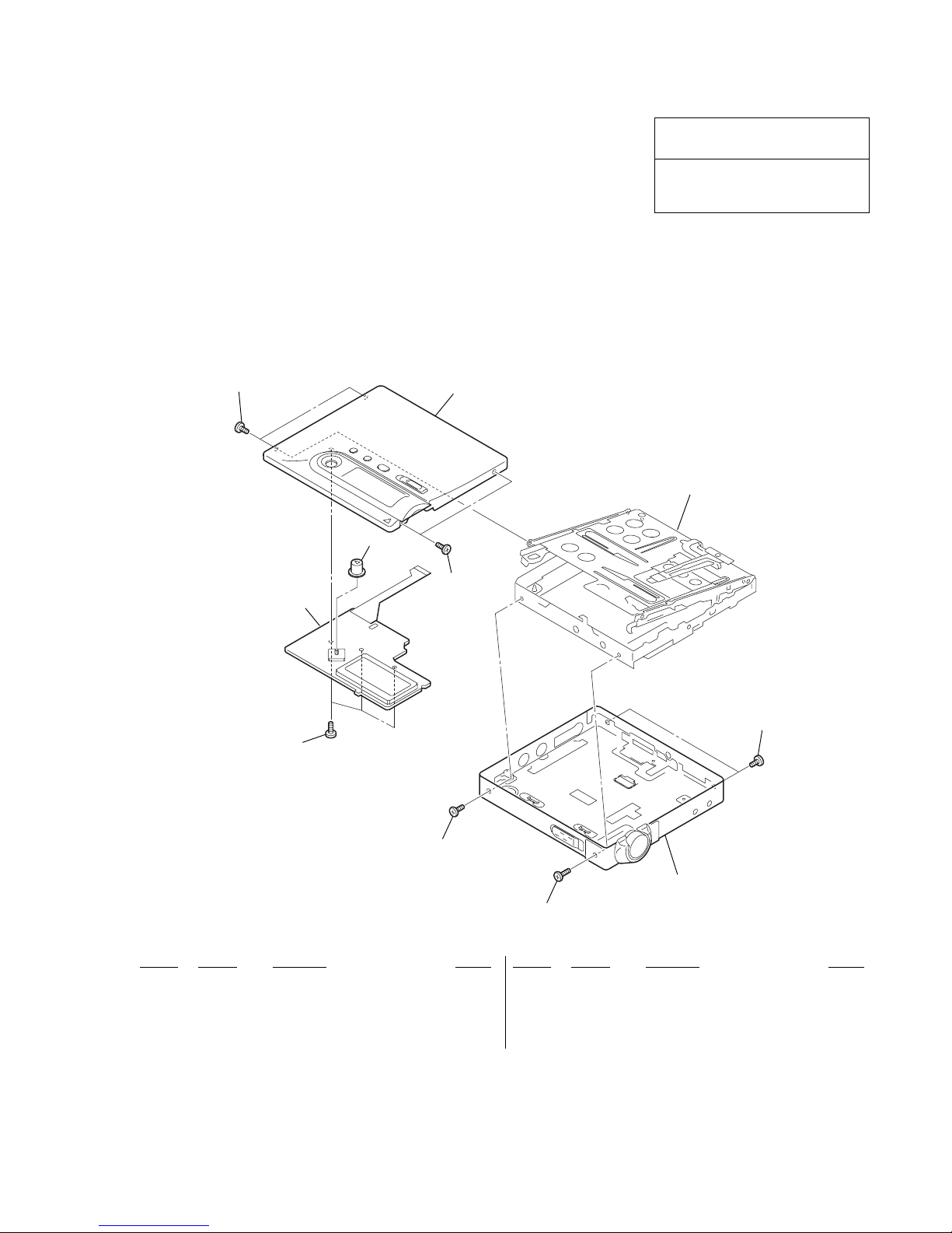
55
MZ-N10
SECTION 7
EXPLODED VIEWS
• Accessories are given in the last of the electrical parts list.
•Abbreviation
CND :Canadian model
3CED :Spanish,Swedish,Portuguese and
Finnish model
4CED :French,German,Italian and Dutch
model
KR :Korean model
TW :Taiwan model
E18 : 100-240V AC Area in E model
CH :Chinese model
JE :Tourist model
NOTE:
• -XX and -X mean standardized parts, so they
may have some difference from the original
one.
• Color Indication of Appearance Parts
Example:
KNOB, BALANCE (WHITE) . . . (RED)
↑↑
Parts Color Cabinet's Color
• Items marked “*” are not stocked since they
are seldom required for routine service. Some
delay should be anticipated when ordering
these items.
• The mechanical parts with no reference number in the exploded views are not supplied.
The components identified by mark 0 or
dotted line with mark 0 are critical for safety.
Replace only with part number specified.
Les composants identifiés par une marque
0 sont critiques pour la sécurité.
Ne les remplacer que par une pièce portant
le numéro spécifié.
7-1. Upper Panel Section
Ref. No. Part No. Description Remark Ref. No. Part No. Description Remark
1 4-984-017-01 SCREW (1.7), TAPPING
2 1-804-970-11 LCD MODULE
3 3-246-979-01 BUTTON (CONTROL B)
4 3-234-449-09 SCREW (M1.4) (GRAY) (HK,KR,E18,CH)
4 3-234-449-11 SCREW (M1.4) (SILVER)
5 3-225-873-25 SCREW (M1.4) (SILVER)
5 3-225-873-27 SCREW (M1.4) (GRAY) (HK,KR,E18,CH)
6 X-3383-355-1 UPPER PANEL SUB ASSY (SILVER)
6 X-3383-356-1 UPPER PANEL SUB ASSY (GRAY)
(HK,KR,E18,CH)
chassis section
bottom panel section
1
2
3
4
4
6
4
5
4
Ver 1.2 2003.02
Page 56
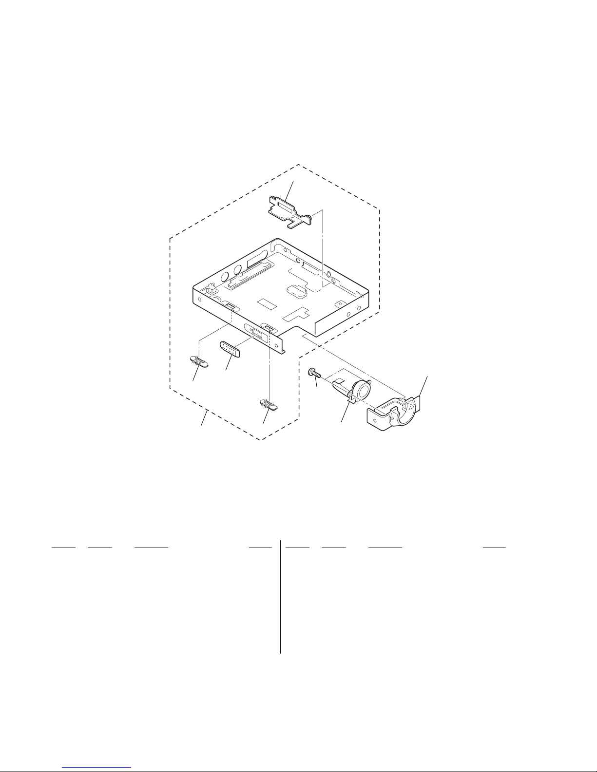
56
MZ-N10
7-2. Bottom Panel Section
Ref. No. Part No. Description Remark
Ref. No. Part No. Description Remark
51
52
53
54
55
56
57
58
51 X-3383-400-1 SERVICE ASSY, PANEL (S-CE) (SILVER)
(3CED,4CED,UK)
51 X-3383-402-1 SERVICE ASSY, PANEL (S-JE) (SILVER) (JE)
51 X-3383-404-1 SERVICE ASSY, PANEL (S-NONCE) (SILVER)
(US,CND,HK,KR,TW,E18,CH)
51 X-3383-405-1 SERVICE ASSY, PANEL (H-NONCE) (GRAY)
(HK,KR,E18,CH)
52 3-247-001-01 KNOB (BATT) (SILVER)
52 3-247-001-11 KNOB (BATT) (GRAY) (HK,KR,E18,CH)
53 3-247-005-01 KNOB (OPEN)
54 3-247-000-01 KNOB (HOLD) (SILVER)
54 3-247-000-11 KNOB (HOLD) (GRAY) (HK,KR,E18,CH)
55 3-247-006-01 ESCUTCHEON (CONNECTOR) (SILVER)
55 3-247-006-11 ESCUTCHEON (CONNECTOR) (GRAY)
(HK,KR,E18,CH)
56 4-984-017-91 SCREW (1.7), TAPPING
57 1-477-512-11 SWITCH UNIT (WITH JOG DIAL)
58 X-3383-353-1 ORNAMENT (JOG) SUB ASSY (SILVER)
58 X-3383-354-1 ORNAMENT (JOG) SUB ASSY (GRAY)
(HK,KR,E18,CH)
Ver 1.2 2003.02
Page 57
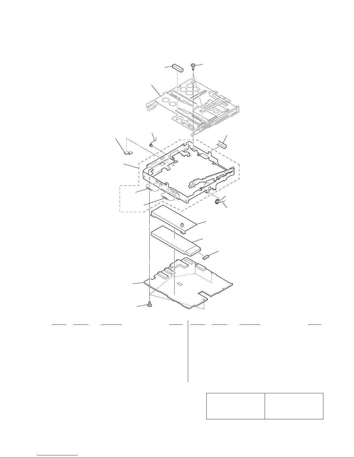
57
MZ-N10
7-3. Chassis Section
Ref. No. Part No. Description Remark
Ref. No. Part No. Description Remark
101
102
103
104
105
106
107
108
109
110
112
113
111
114
MD mechanism deck
(MT-MZN10-181)
101 3-238-876-07 SCREW (M1.4), TOOTHED LOCK
102 A-3663-958-B MAIN BOARD, COMPLETE
(EXCEPT,3CED,4CED,UK)
102 A-3663-959-B MAIN BOARD, COMPLETE (3CED,4CED,UK)
103 3-247-009-01 CUSHION (BATTERY)
0 104 1-756-318-21 BATTERY, LITHIUM ION STORAGE (US,CND)
0 104 1-756-318-31 BATTERY, LITHIUM ION STORAGE
(EXCEPT US,CND)
105 3-246-993-01 CASE, BATTERY
106 3-246-995-01 SPRING (POP-R), TORSION
107 3-246-997-01 SPRING (OPEN), EXTENSION
108 3-246-998-01 SPRING (LOCK) (POWER TENSION)
109 X-3382-681-1 CHASSIS ASSY, SET
110 3-246-994-01 SPRING (POP-L), TORSION
111 3-246-996-01 SCREW (MD), STEP
112 3-251-164-01 SPACER (10P)
113 3-251-161-01 SPACER (MIC)
114 3-251-939-01 SPACER (HOLDER)
Ver 1.2 2003.02
The components identified by
mark 0 or dotted line with mark
0 are critical for safety.
Replace only with part number
specified.
Les composants identifiés par
une marque 0 sont critiques
pour la sécurité.
Ne les remplacer que par une
pièce portant le numéro spécifié.
Page 58
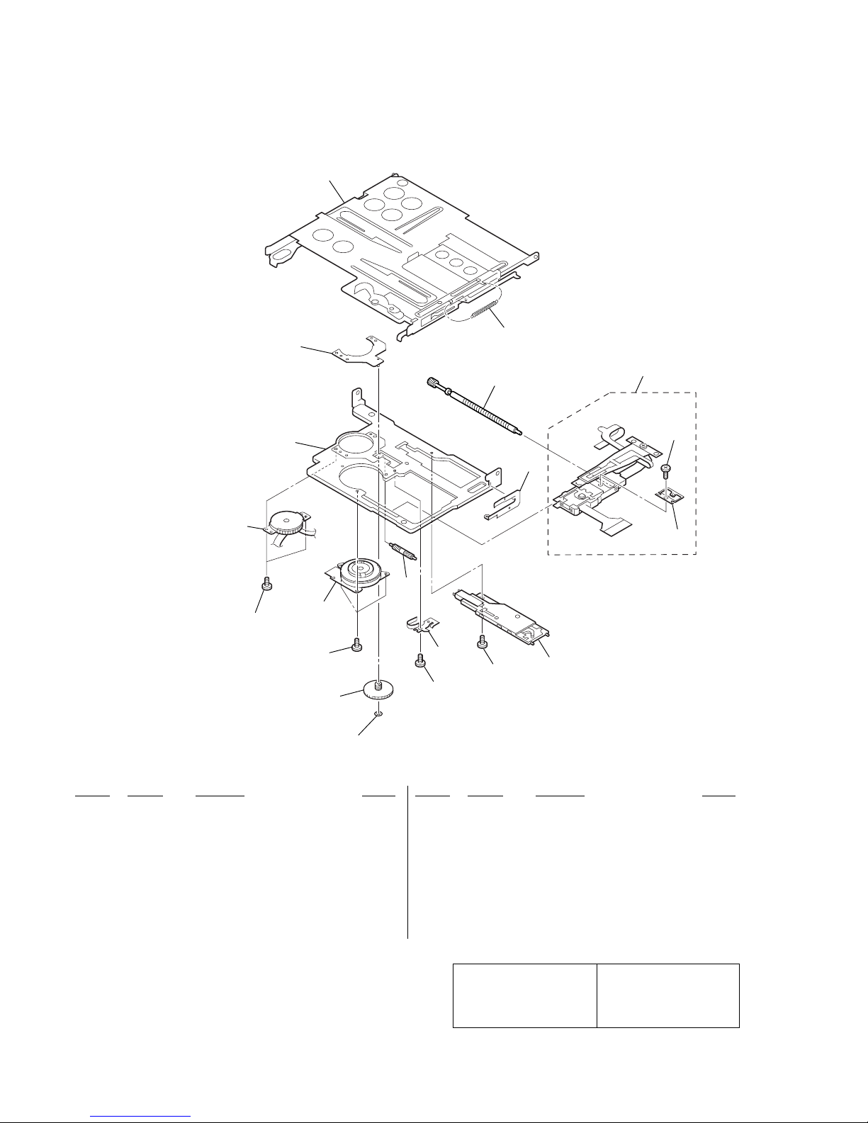
58
MZ-N10
7-4. MD Mechanism Deck Section
(MT-MZN10-181)
Ref. No. Part No. Description Remark
Ref. No. Part No. Description Remark
M601
M603
M602
151
152
153
157
157
158
159
161
162
163
164
160
165
153
155
156
153
151 3-338-645-31 WASHER (0.8-2.5)
152 3-244-882-01 GEAR (SA)
153 3-225-278-02 SCREW, TAPPING
155 3-244-880-01 SPRING, ***
156 3-244-883-01 GEAR (SB)
157 3-225-996-17 SCREW (M1.4)(EG),PRECISION PAN
158 3-245-013-01 CHASSIS (REC)
159 3-245-021-01 PLATE, RATCHET
0 160 X-3382-955-1 OP SERVICE ASSY (ABX-1R)
161 A-3174-607-A SCREW BLOCK ASSY, LEAD
162 X-3382-398-1 BASE ASSY, MOTOR
163 X-3382-416-1 HOLDER ASSY
164 3-245-020-01 SPRING (EJECT), TENSION
165 3-244-879-01 SPRING, RACK
M601 8-835-782-01 MOTOR, DC SSM18D/C-NP (SPINDLE)
M602 8-835-778-01 MOTOR, DC SSM21A/C-NP (SLED)
M603 1-477-519-11 MOTOR UNIT, DC (OVER WRITE HEAD UP/
DOWN)
The components identified by
mark 0 or dotted line with mark
0 are critical for safety.
Replace only with part number
specified.
Les composants identifiés par
une marque 0 sont critiques
pour la sécurité.
Ne les remplacer que par une
pièce portant le numéro spécifié.
Ver 1.2 2003.02
Page 59
59
MZ-N10
SECTION 8
ELECTRICAL PARTS LIST
NOTE:
• Due to standardization, replacements in the
parts list may be different from the parts specified in the diagrams or the components used
on the set.
• -XX and -X mean standardized parts, so they
may have some difference from the original one.
• RESISTORS
All resistors are in ohms.
METAL: Metal-film resistor.
METAL OXIDE: Metal oxide-film resistor.
F: nonflammable
• Items marked “*” are not stocked since they
are seldom required for routine service.
Some delay should be anticipated when ordering these items.
• SEMICONDUCTORS
In each case, u: µ, for example:
uA. . : µA. . uPA. . : µPA. .
uPB. . : µPB. . uPC. . : µPC. .
uPD. . : µPD. .
• CAPACITORS
uF: µF
• COILS
uH: µH
•Abbreviation
CND :Canadian model
3CED :Spanish,Swedish,Portuguese and
Finnish model
4CED :French,German,Italian and Dutch
model
When indicating parts by reference number,
please include the board name.
The components identified by mark 0 or
dotted line with mark 0 are critical for safety.
Replace only with part number specified.
Les composants identifiés par une marque
0 sont critiques pour la sécurité.
Ne les remplacer que par une pièce portant
le numéro spécifié.
KR :Korean model
TW :Taiwan model
E18 : 100-240V AC Area in E model
CH :Chinese model
JE :Tourist model
MAIN
Ver 1.2 2003.02
Ref. No. Part No. Description Remark Ref. No. Part No. Description Remark
A-3663-958-B MAIN BOARD, COMPLETE
(EXCEPT,3CED,4CED,UK)
A-3663-959-B MAIN BOARD, COMPLETE (3CED,4CED,UK)
*********************
3-251-171-01 SPACER (***)
< CAPACITOR >
C101 1-164-939-11 CERAMIC CHIP 0.0022uF 10.00% 50V
C102 1-125-777-11 CERAMIC CHIP 0.1uF 10.00% 10V
C103 1-164-937-11 CERAMIC CHIP 0.001uF 10.00% 50V
C104 1-164-874-11 CERAMIC CHIP 100PF 5.00% 50V
C105 1-125-837-91 CERAMIC CHIP 1uF 10% 6.3V
C106 1-125-926-91 TANTAL. CHIP 4.7uF 20% 6.3V
C107 1-131-725-91 TANTAL. CHIP 47uF 20% 4V
C110 1-164-943-11 CERAMIC CHIP 0.01uF 10.00% 16V
C111 1-135-868-91 TANTAL. CHIP 220uF 20% 2.5V
C112 1-113-600-11 TANTAL. CHIP 2.2uF 20.00% 6.3V
C113 1-164-935-11 CERAMIC CHIP 470PF 10.00% 50V
C114 1-164-941-11 CERAMIC CHIP 0.0047uF 10.00% 16V
C115 1-164-939-11 CERAMIC CHIP 0.0022uF 10.00% 50V
C116 1-125-837-91 CERAMIC CHIP 1uF 10% 6.3V
C201 1-164-939-11 CERAMIC CHIP 0.0022uF 10.00% 50V
C202 1-125-777-11 CERAMIC CHIP 0.1uF 10.00% 10V
C203 1-164-937-11 CERAMIC CHIP 0.001uF 10.00% 50V
C204 1-164-874-11 CERAMIC CHIP 100PF 5.00% 50V
C205 1-125-837-91 CERAMIC CHIP 1uF 10% 6.3V
C206 1-125-926-91 TANTAL. CHIP 4.7uF 20% 6.3V
C207 1-131-725-91 TANTAL. CHIP 47uF 20% 4V
C210 1-164-943-11 CERAMIC CHIP 0.01uF 10.00% 16V
C211 1-135-868-91 TANTAL. CHIP 220uF 20% 2.5V
C212 1-113-600-11 TANTAL. CHIP 2.2uF 20.00% 6.3V
C213 1-164-935-11 CERAMIC CHIP 470PF 10.00% 50V
C214 1-164-941-11 CERAMIC CHIP 0.0047uF 10.00% 16V
C215 1-164-939-11 CERAMIC CHIP 0.0022uF 10.00% 50V
C216 1-125-837-91 CERAMIC CHIP 1uF 10% 6.3V
C301 1-117-919-11 TANTAL. CHIP 10uF 20.00% 6.3V
C303 1-164-937-11 CERAMIC CHIP 0.001uF 10.00% 50V
C306 1-125-777-11 CERAMIC CHIP 0.1uF 10.00% 10V
C307 1-164-937-11 CERAMIC CHIP 0.001uF 10.00% 50V
C308 1-164-937-11 CERAMIC CHIP 0.001uF 10.00% 50V
C310 1-125-777-11 CERAMIC CHIP 0.1uF 10.00% 10V
C311 1-117-919-11 TANTAL. CHIP 10uF 20.00% 6.3V
C312 1-125-777-11 CERAMIC CHIP 0.1uF 10.00% 10V
C313 1-125-777-11 CERAMIC CHIP 0.1uF 10.00% 10V
C314 1-125-839-91 TANTAL. CHIP 47uF 20.00% 6.3V
C315 1-113-600-11 TANTAL. CHIP 2.2uF 20.00% 6.3V
C316 1-125-777-11 CERAMIC CHIP 0.1uF 10.00% 10V
C317 1-113-600-11 TANTAL. CHIP 2.2uF 20.00% 6.3V
C318 1-125-839-91 TANTAL. CHIP 47uF 20.00% 6.3V
C319 1-125-777-11 CERAMIC CHIP 0.1uF 10.00% 10V
C320 1-125-840-91 TANTALUM 10uF 20.00% 6.3V
C321 1-100-453-91 CAP, CHIP TANTALUM ELECT 22uF
C322 1-125-777-11 CERAMIC CHIP 0.1uF 10.00% 10V
C323 1-164-939-11 CERAMIC CHIP 0.0022uF 10.00% 50V
C324 1-125-837-91 CERAMIC CHIP 1uF 10% 6.3V
C325 1-125-926-91 TANTAL. CHIP 4.7uF 20% 6.3V
C326 1-113-600-11 TANTAL. CHIP 2.2uF 20.00% 6.3V
C327 1-127-895-91 TANTAL. CHIP 22uF 20% 4V
C328 1-125-839-91 TANTAL. CHIP 47uF 20.00% 6.3V
C329 1-131-725-91 TANTAL. CHIP 47uF 20% 4V
C330 1-131-725-91 TANTAL. CHIP 47uF 20% 4V
C331 1-131-725-91 TANTAL. CHIP 47uF 20% 4V
C332 1-131-725-91 TANTAL. CHIP 47uF 20% 4V
C333 1-131-725-91 TANTAL. CHIP 47uF 20% 4V
C334 1-164-943-11 CERAMIC CHIP 0.01uF 10.00% 16V
C335 1-100-453-91 CAP, CHIP TANTALUM ELECT 22uF
C336 1-127-895-91 TANTAL. CHIP 22uF 20% 4V
C337 1-125-839-91 TANTAL. CHIP 47uF 20.00% 6.3V
C339 1-164-937-11 CERAMIC CHIP 0.001uF 10.00% 50V
C340 1-164-937-11 CERAMIC CHIP 0.001uF 10.00% 50V
C341 1-164-943-11 CERAMIC CHIP 0.01uF 10.00% 16V
C342 1-164-937-11 CERAMIC CHIP 0.001uF 10.00% 50V
C343 1-164-937-11 CERAMIC CHIP 0.001uF 10.00% 50V
C344 1-125-777-11 CERAMIC CHIP 0.1uF 10.00% 10V
C345 1-125-839-91 TANTAL. CHIP 47uF 20.00% 6.3V
C347 1-164-937-11 CERAMIC CHIP 0.001uF 10.00% 50V
C501 1-125-837-91 CERAMIC CHIP 1uF 10% 6.3V
C502 1-125-777-11 CERAMIC CHIP 0.1uF 10.00% 10V
C503 1-125-837-91 CERAMIC CHIP 1uF 10% 6.3V
C504 1-125-926-91 TANTAL. CHIP 4.7uF 20% 6.3V
C505 1-125-840-91 TANTALUM 10uF 20.00% 6.3V
C506 1-164-943-11 CERAMIC CHIP 0.01uF 10.00% 16V
C507 1-117-919-11 TANTAL. CHIP 10uF 20.00% 6.3V
C508 1-125-777-11 CERAMIC CHIP 0.1uF 10.00% 10V
C509 1-125-777-11 CERAMIC CHIP 0.1uF 10.00% 10V
C510 1-125-840-91 TANTALUM 10uF 20.00% 6.3V
C511 1-164-850-11 CERAMIC CHIP 10PF 0.50PF 50V
Page 60

60
MZ-N10
C520 1-125-777-11 CERAMIC CHIP 0.1uF 10.00% 10V
C522 1-125-777-11 CERAMIC CHIP 0.1uF 10.00% 10V
C523 1-164-939-11 CERAMIC CHIP 0.0022uF 10.00% 50V
C524 1-125-837-91 CERAMIC CHIP 1uF 10% 6.3V
C526 1-119-923-81 CERAMIC CHIP 0.047uF 10.00% 10V
C527 1-164-941-11 CERAMIC CHIP 0.0047uF 10.00% 16V
C528 1-125-837-91 CERAMIC CHIP 1uF 10% 6.3V
C533 1-164-943-11 CERAMIC CHIP 0.01uF 10.00% 16V
C534 1-164-941-11 CERAMIC CHIP 0.0047uF 10.00% 16V
C535 1-125-837-91 CERAMIC CHIP 1uF 10% 6.3V
C536 1-125-777-11 CERAMIC CHIP 0.1uF 10.00% 10V
C537 1-107-819-11 CERAMIC CHIP 0.022uF 10.00% 16V
C538 1-107-819-11 CERAMIC CHIP 0.022uF 10.00% 16V
C540 1-164-941-11 CERAMIC CHIP 0.0047uF 10.00% 16V
C543 1-164-858-11 CERAMIC CHIP 22PF 5.00% 50V
C544 1-164-858-11 CERAMIC CHIP 22PF 5.00% 50V
C545 1-164-858-11 CERAMIC CHIP 22PF 5.00% 50V
C546 1-164-858-11 CERAMIC CHIP 22PF 5.00% 50V
C547 1-164-858-11 CERAMIC CHIP 22PF 5.00% 50V
C548 1-164-858-11 CERAMIC CHIP 22PF 5.00% 50V
C549 1-164-858-11 CERAMIC CHIP 22PF 5.00% 50V
C551 1-164-858-11 CERAMIC CHIP 22PF 5.00% 50V
C552 1-125-837-91 CERAMIC CHIP 1uF 10% 6.3V
C554 1-125-777-11 CERAMIC CHIP 0.1uF 10.00% 10V
C602 1-125-840-91 TANTALUM 10uF 20.00% 6.3V
C603 1-137-704-91 TANTAL. CHIP 10uF 20% 10V
C604 1-125-840-91 TANTALUM 10uF 20.00% 6.3V
C605 1-117-919-11 TANTAL. CHIP 10uF 20.00% 6.3V
C606 1-107-820-11 CERAMIC CHIP 0.1uF 16V
C608 1-125-839-91 TANTAL. CHIP 47uF 20.00% 6.3V
C609 1-107-820-11 CERAMIC CHIP 0.1uF 16V
C610 1-164-941-11 CERAMIC CHIP 0.0047uF 10.00% 16V
C611 1-131-860-91 TANTAL. CHIP 4.7uF 20% 10V
C612 1-125-777-11 CERAMIC CHIP 0.1uF 10.00% 10V
C614 1-107-820-11 CERAMIC CHIP 0.1uF 16V
C615 1-164-943-11 CERAMIC CHIP 0.01uF 10.00% 16V
C617 1-128-694-91 TANTAL. CHIP 22uF 20% 10V
C618 1-128-694-91 TANTAL. CHIP 22uF 20% 10V
C619 1-164-943-11 CERAMIC CHIP 0.01uF 10.00% 16V
C621 1-125-839-91 TANTAL. CHIP 47uF 20.00% 6.3V
C622 1-125-837-91 CERAMIC CHIP 1uF 10% 6.3V
C623 1-125-777-11 CERAMIC CHIP 0.1uF 10.00% 10V
C625 1-125-777-11 CERAMIC CHIP 0.1uF 10.00% 10V
C626 1-125-840-91 TANTALUM 10uF 20.00% 6.3V
C627 1-164-943-11 CERAMIC CHIP 0.01uF 10.00% 16V
C701 1-107-819-11 CERAMIC CHIP 0.022uF 10.00% 16V
C702 1-107-819-11 CERAMIC CHIP 0.022uF 10.00% 16V
C703 1-107-819-11 CERAMIC CHIP 0.022uF 10.00% 16V
C707 1-164-943-11 CERAMIC CHIP 0.01uF 10.00% 16V
C708 1-164-943-11 CERAMIC CHIP 0.01uF 10.00% 16V
C709 1-164-943-11 CERAMIC CHIP 0.01uF 10.00% 16V
C710 1-107-819-11 CERAMIC CHIP 0.022uF 10.00% 16V
C711 1-107-819-11 CERAMIC CHIP 0.022uF 10.00% 16V
C712 1-107-819-11 CERAMIC CHIP 0.022uF 10.00% 16V
C715 1-107-820-11 CERAMIC CHIP 0.1uF 16V
C716 1-107-820-11 CERAMIC CHIP 0.1uF 16V
C718 1-107-820-11 CERAMIC CHIP 0.1uF 16V
C719 1-107-820-11 CERAMIC CHIP 0.1uF 16V
C720 1-107-820-11 CERAMIC CHIP 0.1uF 16V
C721 1-107-820-11 CERAMIC CHIP 0.1uF 16V
C801 1-125-926-91 TANTAL. CHIP 4.7uF 20% 6.3V
C802 1-125-777-11 CERAMIC CHIP 0.1uF 10.00% 10V
C803 1-107-820-11 CERAMIC CHIP 0.1uF 16V
C804 1-117-919-11 TANTAL. CHIP 10uF 20.00% 6.3V
C805 1-125-840-91 TANTALUM 10uF 20.00% 6.3V
C806 1-125-839-91 TANTAL. CHIP 47uF 20.00% 6.3V
C807 1-125-839-91 TANTAL. CHIP 47uF 20.00% 6.3V
C808 1-164-937-11 CERAMIC CHIP 0.001uF 10.00% 50V
C809 1-164-840-11 CERAMIC CHIP 1PF 0.25PF 50V
C810 1-164-840-11 CERAMIC CHIP 1PF 0.25PF 50V
C811 1-125-837-91 CERAMIC CHIP 1uF 10% 6.3V
C812 1-125-837-91 CERAMIC CHIP 1uF 10% 6.3V
C813 1-164-943-11 CERAMIC CHIP 0.01uF 10.00% 16V
C814 1-125-891-11 CERAMIC CHIP 0.47uF 10.00% 10V
C815 1-164-935-11 CERAMIC CHIP 470PF 10.00% 50V
C817 1-125-837-91 CERAMIC CHIP 1uF 10% 6.3V
C818 1-125-777-11 CERAMIC CHIP 0.1uF 10.00% 10V
C819 1-125-777-11 CERAMIC CHIP 0.1uF 10.00% 10V
C820 1-164-943-11 CERAMIC CHIP 0.01uF 10.00% 16V
C821 1-107-819-11 CERAMIC CHIP 0.022uF 10.00% 16V
C822 1-164-943-11 CERAMIC CHIP 0.01uF 10.00% 16V
C823 1-107-819-11 CERAMIC CHIP 0.022uF 10.00% 16V
C825 1-164-943-11 CERAMIC CHIP 0.01uF 10.00% 16V
C826 1-164-943-11 CERAMIC CHIP 0.01uF 10.00% 16V
C827 1-125-777-11 CERAMIC CHIP 0.1uF 10.00% 10V
C829 1-164-941-11 CERAMIC CHIP 0.0047uF 10.00% 16V
C830 1-125-777-11 CERAMIC CHIP 0.1uF 10.00% 10V
C831 1-107-820-11 CERAMIC CHIP 0.1uF 16V
C832 1-107-820-11 CERAMIC CHIP 0.1uF 16V
C833 1-107-820-11 CERAMIC CHIP 0.1uF 16V
C834 1-107-819-11 CERAMIC CHIP 0.022uF 10.00% 16V
C851 1-107-820-11 CERAMIC CHIP 0.1uF 16V
C861 1-125-777-11 CERAMIC CHIP 0.1uF 10.00% 10V
C862 1-125-777-11 CERAMIC CHIP 0.1uF 10.00% 10V
C863 1-125-777-11 CERAMIC CHIP 0.1uF 10.00% 10V
C864 1-125-777-11 CERAMIC CHIP 0.1uF 10.00% 10V
C865 1-125-777-11 CERAMIC CHIP 0.1uF 10.00% 10V
C866 1-164-842-11 CERAMIC CHIP 2PF 0.25PF 50V
C891 1-164-941-11 CERAMIC CHIP 0.0047uF 10.00% 16V
C902 1-100-352-91 CAP, CHIP CERAMIC 1uF B (1608)
C904 1-125-777-11 CERAMIC CHIP 0.1uF 10.00% 10V
C906 1-164-935-11 CERAMIC CHIP 470PF 10.00% 50V
C907 1-125-777-11 CERAMIC CHIP 0.1uF 10.00% 10V
C908 1-100-352-91 CAP, CHIP CERAMIC 1uF B (1608)
C909 1-135-957-91 TANTAL. CHIP 10uF 20% 16V
C910 1-125-837-91 CERAMIC CHIP 1uF 10% 6.3V
C911 1-164-943-11 CERAMIC CHIP 0.01uF 10.00% 16V
C912 1-119-923-81 CERAMIC CHIP 0.047uF 10.00% 10V
C914 1-164-937-11 CERAMIC CHIP 0.001uF 10.00% 50V
C915 1-125-840-91 TANTALUM 10uF 20.00% 6.3V
C916 1-125-840-91 TANTALUM 10uF 20.00% 6.3V
C917 1-125-840-91 TANTALUM 10uF 20.00% 6.3V
C918 1-107-820-11 CERAMIC CHIP 0.1uF 16V
C919 1-125-839-91 TANTAL. CHIP 47uF 20.00% 6.3V
C920 1-125-840-91 TANTALUM 10uF 20.00% 6.3V
MAIN
Ref. No. Part No. Description Remark Ref. No. Part No. Description Remark
Page 61
61
MZ-N10
C921 1-125-840-91 TANTALUM 10uF 20.00% 6.3V
C922 1-125-777-11 CERAMIC CHIP 0.1uF 10.00% 10V
C923 1-107-820-11 CERAMIC CHIP 0.1uF 16V
C924 1-131-725-91 TANTAL. CHIP 47uF 20% 4V
C925 1-164-941-11 CERAMIC CHIP 0.0047uF 10.00% 16V
C926 1-107-820-11 CERAMIC CHIP 0.1uF 16V
C927 1-125-840-91 TANTALUM 10uF 20.00% 6.3V
C929 1-164-943-11 CERAMIC CHIP 0.01uF 10.00% 16V
C932 1-125-837-91 CERAMIC CHIP 1uF 10% 6.3V
C933 1-125-777-11 CERAMIC CHIP 0.1uF 10.00% 10V
C936 1-135-957-91 TANTAL. CHIP 10uF 20% 16V
C937 1-135-957-91 TANTAL. CHIP 10uF 20% 16V
C938 1-137-910-11 TANTAL. CHIP 10uF 20% 16V
C951 1-100-353-91 CAP,CHIP CERAMIC 4.7uF B (3225)
C952 1-128-694-91 TANTAL. CHIP 22uF 20% 10V
C953 1-125-777-11 CERAMIC CHIP 0.1uF 10.00% 10V
C954 1-164-941-11 CERAMIC CHIP 0.0047uF 10.00% 16V
C955 1-128-694-91 TANTAL. CHIP 22uF 20% 10V
C956 1-128-694-91 TANTAL. CHIP 22uF 20% 10V
C957 1-107-820-11 CERAMIC CHIP 0.1uF 16V
C958 1-128-694-91 TANTAL. CHIP 22uF 20% 10V
C959 1-125-777-11 CERAMIC CHIP 0.1uF 10.00% 10V
C960 1-115-467-11 CERAMIC CHIP 0.22uF 10.00% 10V
C961 1-100-353-91 CAP,CHIP CERAMIC 4.7uF B (3225)
C962 1-125-777-11 CERAMIC CHIP 0.1uF 10.00% 10V
C966 1-100-352-91 CAP, CHIP CERAMIC 1uF B (1608)
C967 1-125-777-11 CERAMIC CHIP 0.1uF 10.00% 10V
C968 1-100-352-91 CAP, CHIP CERAMIC 1uF B (1608)
< CONNECTOR >
CN501 1-816-934-21 CONNECTOR, FPC (ZIF)
CN701 1-816-935-21 CONNECTOR, FPC (ZIF)
* CN871 1-794-756-21 CONNECTOR, FPC (ZIF) 15P
CN891 1-817-277-21 CONNECTOR, FPC (ZIF)
CN951 1-817-122-21 CONNECTOR, FFC/FPC (ZIF) 5P
CN952 1-816-943-21 CONNECTOR
< DIODE >
D201 8-719-046-90 DIODE MA2S111-TX
D301 8-719-046-91 DIODE MA2S111-TX
D302 8-719-081-71 DIODE DF8A6.8FK(TE85R)
D601 6-500-483-01 DIODE MA22D2800LS0
D602 8-719-081-35 DIODE MA2YD1700LS0
D603 8-719-081-35 DIODE MA2YD1700LS0
D604 6-500-483-01 DIODE MA22D2800LS0
D610 8-719-421-27 DIODE MA728-TX
D801 8-719-421-27 DIODE MA728-TX
D892 8-719-421-27 DIODE MA728-TX
D901 8-719-420-51 DIODE MA729-TX
D902 8-719-404-50 DIODE MA111-TX
D903 8-719-420-51 DIODE MA729-TX
D904 8-719-420-51 DIODE MA729-TX
D952 6-500-483-01 DIODE MA22D2800LS0
< FUSE >
0 F301 1-576-439- FUSE (SMD) 0.25A 125V
< FERRITE BEAD >
FB301 1-216-864-11 METAL CHIP 0 5% 1/10W
FB302 1-216-809-11 METAL CHIP 100 5% 1/10W
FB303 1-469-777-21 FERRITE 0UH
FB304 1-216-864-11 METAL CHIP 0 5% 1/10W
FB801 1-216-864-11 METAL CHIP 0 5% 1/10W
FB802 1-216-864-11 METAL CHIP 0 5% 1/10W
FB803 1-216-864-11 METAL CHIP 0 5% 1/10W
FB804 1-216-864-11 METAL CHIP 0 5% 1/10W
FB805 1-216-864-11 METAL CHIP 0 5% 1/10W
FB952 1-216-864-11 METAL CHIP 0 5% 1/10W
FB953 1-216-864-11 METAL CHIP 0 5% 1/10W
FB954 1-216-864-11 METAL CHIP 0 5% 1/10W
FB955 1-216-864-11 METAL CHIP 0 5% 1/10W
< IC >
IC301 6-702-894-01 IC AK5356VN-L
IC302 6-700-662-01 IC AN17020A-VB
IC501 6-702-869-01 IC SN761058ZQLR
IC502 8-759-565-56 IC XC62HR2202MR
IC503 6-703-691-01 IC XC62HR2502MR
IC601 6-702-866-01 IC SC901581EPR2
IC701 6-702-786-01 IC SC111258EPR2
IC801 8-753-000-74 IC CXD2678-202GA
✩ IC851
——————
IC AK6510L-L (NOT SUPPLIED)
IC861 6-703-011-01 IC TC7SZ126AFE
IC862 6-703-012-01 IC R2061K01-E2
IC901 6-702-865-01 IC SC901580EPR2
IC951 6-702-867-01 IC SC901582EPR2
IC952 8-759-824-57 IC XC61CN3002NR
< JACK >
J301 1-816-945-21 CONNECTOR (MIC (PLUG IN POWER))
J302 1-816-946-21 CONNECTOR (LINE IN (OPT))
J303 1-816-944-11 CONNECTOR (i/LINE IN)
< COIL >
L301 1-469-535-21 INDUCTOR 10uH
L302 1-469-535-21 INDUCTOR 10uH
L303 1-469-535-21 INDUCTOR 10uH
L304 1-469-535-21 INDUCTOR 10uH
L501 1-400-342-21 INDUCTOR 10uH
L502 1-400-342-21 INDUCTOR 10uH
L503 1-400-342-21 INDUCTOR 10uH
L504 1-400-342-21 INDUCTOR 10uH
L601 1-400-305-11 INDUCTOR 47uH
L602 1-456-170-21 INDUCTOR 10uH
L603 1-456-170-21 INDUCTOR 10uH
L604 1-400-342-21 INDUCTOR 10uH
L605 1-400-342-21 INDUCTOR 10uH
L802 1-469-535-21 INDUCTOR 10uH
L803 1-469-535-21 INDUCTOR 10uH
L901 1-400-360-11 INDUCTOR 270uH
MAIN
Ref. No. Part No. Description Remark Ref. No. Part No. Description Remark
✩When IC851 is damaged, replace the MAIN board.
The components identified by mark 0 or dotted line with mark 0 are
critical for safety.
Replace only with part number specified.
Page 62

62
MZ-N10
L902 1-400-362-11 INDUCTOR 330uH
L903 1-400-342-21 INDUCTOR 10uH
L904 1-400-361-11 INDUCTOR 220uH
< TRANSISTOR >
Q301 8-729-051-23 TRANSISTOR 2SA2018TL
Q501 8-729-922-10 TRANSISTOR 2SA1577-T106-QR
Q502 8-729-034-59 TRANSISTOR 2SA1745-6.7-TL
Q503 8-729-429-44 TRANSISTOR XP1501-TXE
Q601 6-550-356-01 TRANSISTOR MCH6616-TL-E
Q602 6-550-357-01 TRANSISTOR CPH5614-TL-E
Q603 6-550-355-01 TRANSISTOR RTQ045N03
Q604 6-550-354-01 TRANSISTOR RTQ035P02
Q605 8-729-046-45 TRANSISTOR SI2302DS-T1
Q606 8-729-030-46 TRANSISTOR XP4314-TX
Q607 8-729-030-46 TRANSISTOR XP4314-TX
Q608 8-729-052-37 TRANSISTOR XP151A13A0MR
Q612 8-729-037-52 TRANSISTOR 2SD2216J-QR(TX).SO
Q901 8-729-051-50 TRANSISTOR XP152A12C0MR
Q902 8-729-051-50 TRANSISTOR XP152A12C0MR
Q904 8-729-037-75 TRANSISTOR UN9214J-(TX).SO
Q951 8-729-037-61 TRANSISTOR UN9113J-(TX).SO
Q952 8-729-030-46 TRANSISTOR XP4314-TX
Q953 8-729-037-52 TRANSISTOR 2SC4738F-Y/GR(TPL3)
Q954 6-550-326-01 TRANSISTOR FZT968TA
Q961 8-729-030-46 TRANSISTOR XP4314-TX
< RESISTOR >
R101 1-208-927-11 METAL CHIP 47K 0.5% 1/16W
R102 1-208-715-11 METAL CHIP 22K 0.5% 1/16W
R103 1-208-715-11 METAL CHIP 22K 0.5% 1/16W
R104 1-208-707-11 METAL CHIP 10K 0.5% 1/16W
R105 1-218-965-11 RES-CHIP 10K 5% 1/16W
R106 1-218-933-11 RES-CHIP 22 5% 1/16W
R108 1-208-707-11 METAL CHIP 10K 0.5% 1/16W
R109 1-208-707-11 METAL CHIP 10K 0.5% 1/16W
R111 1-218-990-11 SHORT CHIP 0
R112 1-242-967-81 RES-CHIP 1 5% 1/16W
R201 1-208-927-11 METAL CHIP 47K 0.5% 1/16W
R202 1-208-715-11 METAL CHIP 22K 0.5% 1/16W
R203 1-208-715-11 METAL CHIP 22K 0.5% 1/16W
R204 1-208-707-11 METAL CHIP 10K 0.5% 1/16W
R205 1-218-965-11 RES-CHIP 10K 5% 1/16W
R206 1-218-933-11 RES-CHIP 22 5% 1/16W
R208 1-208-707-11 METAL CHIP 10K 0.5% 1/16W
R209 1-208-707-11 METAL CHIP 10K 0.5% 1/16W
R211 1-218-990-11 SHORT CHIP 0
R212 1-242-967-81 RES-CHIP 1 5% 1/16W
R301 1-218-941-81 RES-CHIP 100 5% 1/16W
R302 1-218-965-11 RES-CHIP 10K 5% 1/16W
R303 1-218-977-11 RES-CHIP 100K 5% 1/16W
R304 1-218-941-81 RES-CHIP 100 5% 1/16W
R305 1-218-941-81 RES-CHIP 100 5% 1/16W
R306 1-218-941-81 RES-CHIP 100 5% 1/16W
R307 1-218-953-11 RES-CHIP 1K 5% 1/16W
R308 1-218-953-11 RES-CHIP 1K 5% 1/16W
R309 1-218-953-11 RES-CHIP 1K 5% 1/16W
R310 1-208-943-11 METAL CHIP 220K 0.5% 1/16W
R312 1-218-977-11 RES-CHIP 100K 5% 1/16W
R313 1-218-981-11 RES-CHIP 220K 5% 1/16W
R315 1-208-707-11 METAL CHIP 10K 0.5% 1/16W
R317 1-216-864-11 METAL CHIP 0 5% 1/10W
R319 1-218-990-11 SHORT CHIP 0
R320 1-218-990-11 SHORT CHIP 0
R321 1-218-989-11 RES-CHIP 1M 5% 1/16W
R501 1-218-977-11 RES-CHIP 100K 5% 1/16W
R502 1-218-446-11 METAL CHIP 1 5% 1/10W
R503 1-218-446-11 METAL CHIP 1 5% 1/10W
R504 1-218-965-11 RES-CHIP 10K 5% 1/16W
R505 1-218-965-11 RES-CHIP 10K 5% 1/16W
R507 1-208-707-11 METAL CHIP 10K 0.5% 1/16W
R508 1-218-953-11 RES-CHIP 1K 5% 1/16W
R509 1-218-990-11 SHORT CHIP 0
R511 1-218-990-11 SHORT CHIP 0
R512 1-220-804-11 RES-CHIP 2.2M 5% 1/16W
R513 1-218-981-11 RES-CHIP 220K 5% 1/16W
R514 1-218-973-11 RES-CHIP 47K 5% 1/16W
R515 1-218-965-11 RES-CHIP 10K 5% 1/16W
R516 1-218-977-11 RES-CHIP 100K 5% 1/16W
R517 1-218-965-11 RES-CHIP 10K 5% 1/16W
R518 1-218-973-11 RES-CHIP 47K 5% 1/16W
R602 1-218-973-11 RES-CHIP 47K 5% 1/16W
R603 1-208-635-11 RES-CHIP 10 5% 1/16W
R606 1-208-635-11 RES-CHIP 10 5% 1/16W
R610 1-218-957-11 RES-CHIP 2.2K 5% 1/16W
R612 1-218-446-11 METAL CHIP 1 5% 1/10W
R613 1-220-804-11 RES-CHIP 2.2M 5% 1/16W
R614 1-220-804-11 RES-CHIP 2.2M 5% 1/16W
R617 1-218-977-11 RES-CHIP 100K 5% 1/16W
R618 1-218-953-11 RES-CHIP 1K 5% 1/16W
R619 1-218-945-11 RES-CHIP 220 5% 1/16W
R620 1-208-635-11 RES-CHIP 10 5% 1/16W
R621 1-208-635-11 RES-CHIP 10 5% 1/16W
R622 1-218-977-11 RES-CHIP 100K 5% 1/16W
R625 1-218-977-11 RES-CHIP 100K 5% 1/16W
R626 1-218-981-11 RES-CHIP 220K 5% 1/16W
R627 1-218-953-11 RES-CHIP 1K 5% 1/16W
R630 1-218-990-11 SHORT CHIP 0
R711 1-216-801-11 METAL CHIP 22 5% 1/10W
R712 1-216-801-11 METAL CHIP 22 5% 1/10W
R713 1-216-801-11 METAL CHIP 22 5% 1/10W
R714 1-216-801-11 METAL CHIP 22 5% 1/10W
R802 1-218-953-11 RES-CHIP 1K 5% 1/16W
R803 1-208-635-11 RES-CHIP 10 5% 1/16W
R804 1-208-635-11 RES-CHIP 10 5% 1/16W
R805 1-218-990-11 SHORT CHIP 0
R806 1-218-990-11 SHORT CHIP 0
R807 1-218-965-11 RES-CHIP 10K 5% 1/16W
R808 1-218-965-11 RES-CHIP 10K 5% 1/16W
R809 1-218-977-11 RES-CHIP 100K 5% 1/16W
R811 1-218-981-11 RES-CHIP 220K 5% 1/16W
R813 1-218-953-11 RES-CHIP 1K 5% 1/16W
R814 1-218-957-11 RES-CHIP 2.2K 5% 1/16W
R815 1-218-953-11 RES-CHIP 1K 5% 1/16W
R816 1-218-945-11 RES-CHIP 220 5% 1/16W
R817 1-220-804-11 RES-CHIP 2.2M 5% 1/16W
MAIN
Ref. No. Part No. Description Remark Ref. No. Part No. Description Remark
Page 63

63
MZ-N10
R818 1-218-989-11 RES-CHIP 1M 5% 1/16W
R819 1-208-691-11 METAL CHIP 2.2K 0.5% 1/16W
R820 1-208-691-11 METAL CHIP 2.2K 0.5% 1/16W
R821 1-208-927-11 METAL CHIP 47K 0.5% 1/16W
R822 1-208-943-11 METAL CHIP 220K 0.5% 1/16W
R823 1-218-990-11 SHORT CHIP 0
R824 1-218-985-11 METAL CHIP 470K 0.5% 1/16W
R825 1-218-989-11 RES-CHIP 1M 5% 1/16W
R826 1-218-957-11 RES-CHIP 2.2K 5% 1/16W
R827 1-218-961-11 RES-CHIP 4.7K 5% 1/16W
R828 1-218-933-11 RES-CHIP 22 5% 1/16W
R829 1-218-933-11 RES-CHIP 22 5% 1/16W
R830 1-218-990-11 SHORT CHIP 0
R831 1-218-990-11 SHORT CHIP 0
R832 1-218-990-11 SHORT CHIP 0
R833 1-218-990-11 SHORT CHIP 0
R834 1-208-699-11 METAL CHIP 4.7K 0.5% 1/16W
R835 1-208-699-11 METAL CHIP 4.7K 0.5% 1/16W
R836 1-218-990-11 SHORT CHIP 0
R837 1-208-935-11 METAL CHIP 100K 0.5% 1/16W
R838 1-218-957-11 RES-CHIP 2.2K 5% 1/16W
R839 1-218-990-11 SHORT CHIP 0
R840 1-218-989-11 RES-CHIP 1M 5% 1/16W
R841 1-218-990-11 SHORT CHIP 0
R843 1-218-990-11 SHORT CHIP 0
R844 1-218-990-11 SHORT CHIP 0
R845 1-218-990-11 SHORT CHIP 0
R847 1-208-935-11 METAL CHIP 100K 0.5% 1/16W
R848 1-208-943-11 METAL CHIP 220K 0.5% 1/16W
R849 1-216-864-11 METAL CHIP 0 5% 1/10W
R850 1-218-965-11 RES-CHIP 10K 5% 1/16W
R851 1-218-990-11 SHORT CHIP 0
R852 1-218-977-11 RES-CHIP 100K 5% 1/16W
R853 1-218-977-11 RES-CHIP 100K 5% 1/16W
R856 1-218-990-11 SHORT CHIP 0
R857 1-218-973-11 RES-CHIP 47K 5% 1/16W
R858 1-218-973-11 RES-CHIP 47K 5% 1/16W
R859 1-218-981-11 RES-CHIP 220K 5% 1/16W
R860 1-220-804-11 RES-CHIP 2.2M 5% 1/16W
R871 1-218-990-11 SHORT CHIP 0
R891 1-218-990-11 SHORT CHIP 0
R892 1-218-990-11 SHORT CHIP 0
R893 1-218-990-11 SHORT CHIP 0
R894 1-218-989-11 RES-CHIP 1M 5% 1/16W
R901 1-218-989-11 RES-CHIP 1M 5% 1/16W
R902 1-218-989-11 RES-CHIP 1M 5% 1/16W
R903 1-218-953-11 RES-CHIP 1K 5% 1/16W
R904 1-218-953-11 RES-CHIP 1K 5% 1/16W
R905 1-208-707-11 METAL CHIP 10K 0.5% 1/16W
R907 1-218-985-11 RES-CHIP 470K 5% 1/16W
R908 1-208-927-11 METAL CHIP 47K 0.5% 1/16W
R909 1-208-935-11 METAL CHIP 100K 0.5% 1/16W
R911 1-218-973-11 RES-CHIP 47K 5% 1/16W
R912 1-218-977-11 RES-CHIP 100K 5% 1/16W
R914 1-218-973-11 RES-CHIP 47K 5% 1/16W
R915 1-218-981-11 RES-CHIP 220K 5% 1/16W
R917 1-218-985-11 RES-CHIP 470K 5% 1/16W
R918 1-218-985-11 RES-CHIP 470K 5% 1/16W
R919 1-218-973-11 RES-CHIP 47K 5% 1/16W
R921 1-218-973-11 RES-CHIP 47K 5% 1/16W
R923 1-208-935-11 METAL CHIP 100K 0.5% 1/16W
R926 1-218-969-11 RES-CHIP 22K 5% 1/16W
R929 1-218-981-11 RES-CHIP 220K 5% 1/16W
R931 1-218-990-11 SHORT CHIP 0
R932 1-218-981-11 RES-CHIP 220K 5% 1/16W
R934 1-218-965-11 RES-CHIP 10K 5% 1/16W
R935 1-218-985-11 RES-CHIP 470K 5% 1/16W
R936 1-218-961-11 RES-CHIP 4.7K 5% 1/16W
R951 1-245-457-21 METAL 2.2 1% 1/5W
R952 1-245-454-21 METAL 0.022 1% 1/5W
R953 1-245-456-21 METAL 1 1% 1/5W
R954 1-218-965-11 RES-CHIP 10K 5% 1/16W
R955 1-218-941-81 RES-CHIP 100 5% 1/16W
R956 1-218-969-11 RES-CHIP 22K 5% 1/16W
R957 1-218-977-11 RES-CHIP 100K 5% 1/16W
R958 1-218-941-11 METAL CHIP 100 0.5% 1/16W
R959 1-218-945-11 METAL CHIP 220 0.5% 1/16W
R960 1-218-973-11 RES-CHIP 47K 5% 1/16W
R961 1-216-864-11 METAL CHIP 0 5% 1/10W
R963 1-218-957-11 RES-CHIP 2.2K 5% 1/16W
R964 1-218-973-11 RES-CHIP 47K 5% 1/16W
R974 1-216-864-11 METAL CHIP 0 5% 1/10W
R975 1-216-864-11 METAL CHIP 0 5% 1/10W
R994 1-220-804-11 RES-CHIP 2.2M 5% 1/16W
R995 1-218-981-11 RES-CHIP 220K 5% 1/16W
R997 1-220-804-11 RES-CHIP 2.2M 5% 1/16W
< COMPOSITION CIRCUIT BLOCK >
RB701 1-233-963-21 RES, NETWORK (CHIP TYPE) 2.2K
RB702 1-233-967-11 RES, NETWORK (CHIP TYPE) 10K
< SWITCH >
S801 1-786-448-21 SWITCH, PUSH (1 KEY) (HALF LOCK)
S802 1-786-436-21 SWITCH, SLIDE (HOLD .)
S803 1-786-101-22 SWITCH, DETECTION (OPEN/CLOSE)
S804 1-786-447-21 SWITCH, PUSH (PROTECT)
S805 1-786-446-21 SWITCH, TACTILE (T MARK)
S806 1-786-446-21 SWITCH, TACTILE (END SEARCH)
S951 1-786-436-41 SWITCH, SLIDE (BUILT IN BATTERY)
< VIBRATOR >
X801 1-795-779-21 VIBRATOR, CRYSTAL 22.5792MHz
X802 1-795-780-21 VIBRATOR, CERAMIC 48MHz
X861 1-795-602-11 VIBRATOR, CRYSTAL 32.768kHz
**************************************************************
MAIN
Ref. No. Part No. Description Remark Ref. No. Part No. Description Remark
Page 64
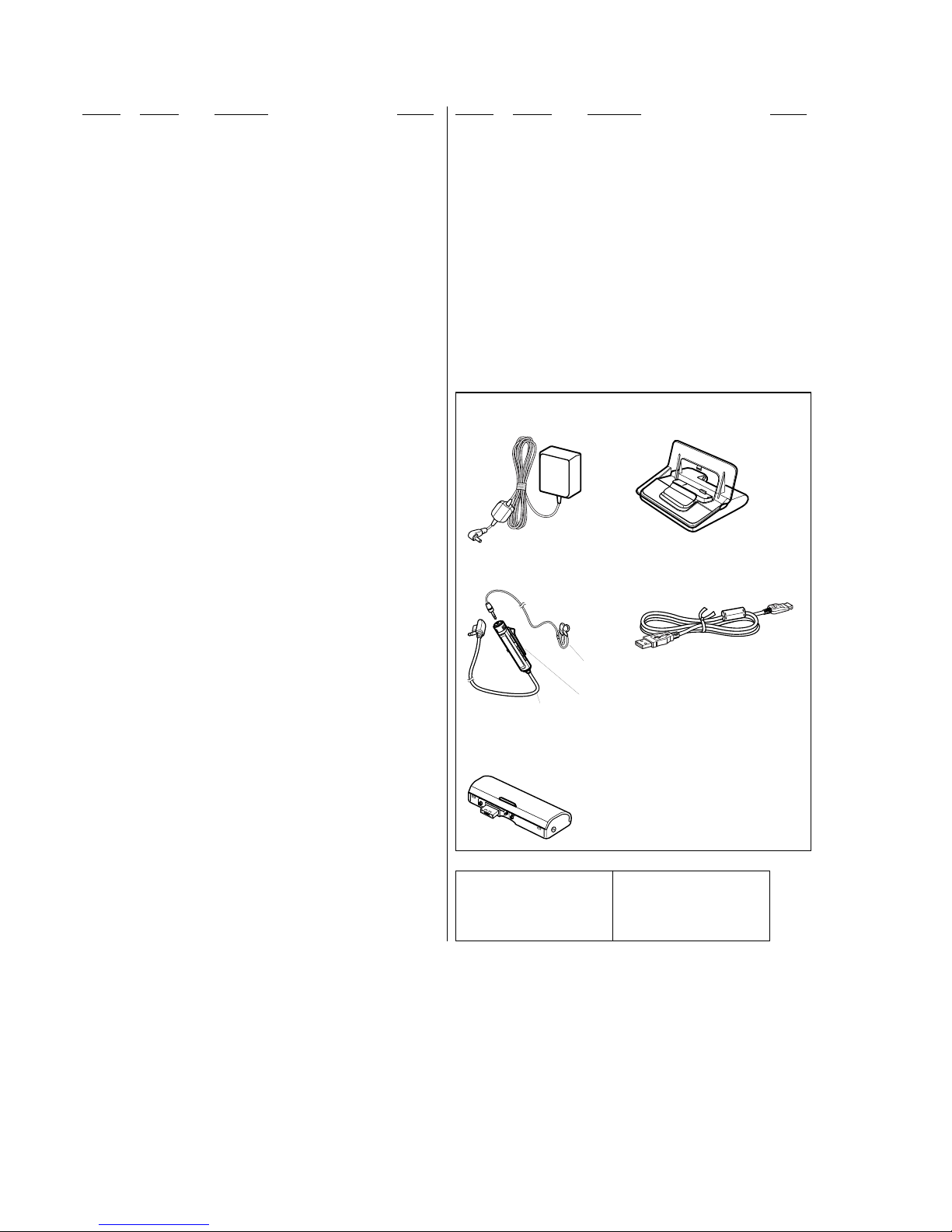
64
MZ-N10
Ref. No. Part No. Description Remark
MISCELLANEOUS
**************
2 1-804-970-11 LCD MODULE
65 1-477-512-11 SWITCH UNIT (WITH JOG DIAL)
0 104 1-756-318-11 BATTERY, LITHIUM ION STORAGE
0 160 X-3382-955-1 OP SERVICE ASSY (ABX-1R)
M601 8-835-782-01 MOTOR, DC SSM18D/C-NP (SPINDLE)
M602 8-835-778-01 MOTOR, DC SSM21A/C-NP (SLED)
M603 1-477-519-11 MOTOR UNIT, DC
(OVER WRITE HEAD UP/DOWN)
**************************************************************
ACCESSORIES
***********
0 1-569-007-12 ADAPTOR, CONVERSION 2P (JE)
1-794-451-11 CONNECTOR, LIGHT (EXCEPT HK,KR,CH,JE)
1-794-451-51 CONNECTOR, LIGHT (HK,KR,CH,JE)
3-021-018-11 LABEL, FRANCE (FR)
3-220-749-01 CASE, CARRYING (HK,KR,TW,E18,CH,JE)
3-228-300-11 CASE, BELT CLIP CARRYING
(CND,3CED,4CED,UK)
3-247-016-01 MANUAL, INSTRUCTION (FRENCH)(CND)
3-250-372-11 MANUAL, INSTRUCTION (ENGLISH)
3-250-372-21 MANUAL, INSTRUCTION (FRENCH)
(US,CND,4CED)
3-250-372-31 MANUAL, INSTRUCTION (GERMAN) (4CED)
3-250-372-41 MANUAL, INSTRUCTION (SPANISH) (3CED,JE)
3-250-372-51 MANUAL, INSTRUCTION (DUTCH) (4CED)
3-250-372-61 MANUAL, INSTRUCTION (SWEDISH) (3CED)
3-250-372-71 MANUAL, INSTRUCTION (ITALIAN) (4CED)
3-250-372-81 MANUAL, INSTRUCTION (PORTUGUESE)
(3CED,JE)
3-250-372-91 MANUAL, INSTRUCTION (FINNISH) (3CED)
3-250-549-11 MANUAL, INSTRUCTION
(TRADITIONAL CHINESE) (HK,TW,E18,JE)
3-250-549-21 MANUAL, INSTRUCTION
(SIMPLIFIED CHINESE) (CH)
3-250-549-31 MANUAL, INSTRUCTION (KOREAN) (JE)
X-3383-268-1 CD-ROM (APPLICATION) ASSY (US,CND)
X-3383-269-3 CD-ROM (APPLICATION) ASSY
(3CED,4CED,UK)
X-3383-270-2 CD-ROM (APPLICATION) ASSY
(HK,KR,TW,E18,CH)
X-3383-271-1 CD-ROM (APPLICATION) ASSY (JE)
0 501 1-477-536-11 ADAPTOR (AC-ES605K), AC (JE)
0 501 1-477-537-11 ADAPTOR (AC-ES605K), AC (HK, UK)
0 501 1-477-538-11 ADAPTOR (AC-ES605K), AC (3CED,4CED)
0 501 1-477-539-11 ADAPTOR (AC-ES605K), AC (US,CND,TW)
Ver 1.2 2003.02
The components identified by
mark 0 or dotted line with mark
0 are critical for safety.
Replace only with part number
specified.
Les composants identifiés par
une marque 0 sont critiques
pour la sécurité.
Ne les remplacer que par une
pièce portant le numéro spécifié.
0 501 1-477-540-11 ADAPTOR (AC-ES605K), AC (E18)
0 501 1-477-541-11 ADAPTOR (AC-ES605K), AC (KR)
0 501 1-477-543-11 ADAPTOR (AC-ES605K), AC (CH)
0 501 1-477-542-11 AC ADAPTOR (AC-ES605K), AC (AUS)
0 502 1-477-513-11 CRADLE UNIT (SILVER)
0 502 1-477-513-21 CRADLE UNIT (GRAY) (HK,KR,E18,CH)
503 1-477-573-11 REMOTE COMMANDER (RM-MC33EL)
504 8-953-218-91 RECEIVER MDR-E838SP/SK SET (EXCEPT US)
504 8-954-019-90 HEADPHONE MDR-A034SP110 (SET)(US)
505 1-824-647-11 CORD, CONNECTION
(EXCEPT 3CED,4CED,UK,KR,TW,CH)
505 1-824-647-21 CORD, CONNECTION
(3CED,4CED,UK,KR,TW,CH)
507 1-417-304-11 BATTERY CASE
508 3-252-648-01 CRIP (REMOTE CONTROL)
Ref. No. Part No. Description Remark
Dedicated USB cradle (1)
AC
power adaptor
USB
cradle
Headphones/earphones
with a remote control (1)
Dry battery case (1)
501 502
505
503
504
507
508
Page 65

65
MZ-N10
MEMO
Page 66
MZ-N10
REVISION HISTORY
Clicking the version allows you to jump to the revised page.
Also, clicking the version at the upper right on the revised page allows you to jump to the next revised
page.
Ver. Date Description of Revision
1.0 2002.12 New
1.1 2003.01 AEP, UK models addition
1.2 2003.02 US,Canadian,Korean,Taiwan,E18 (100-240V AC Area in E model),
Australian,Chinese and Tourist models addition (ENG-03005)
 Loading...