

Page 1
Ver 1.2 2004. 03
9-923-222-14
2004C02-1
© 2004.03
Sony Corporation
Personal Audio Company
Published by Sony Engineering Corporation
Page 2
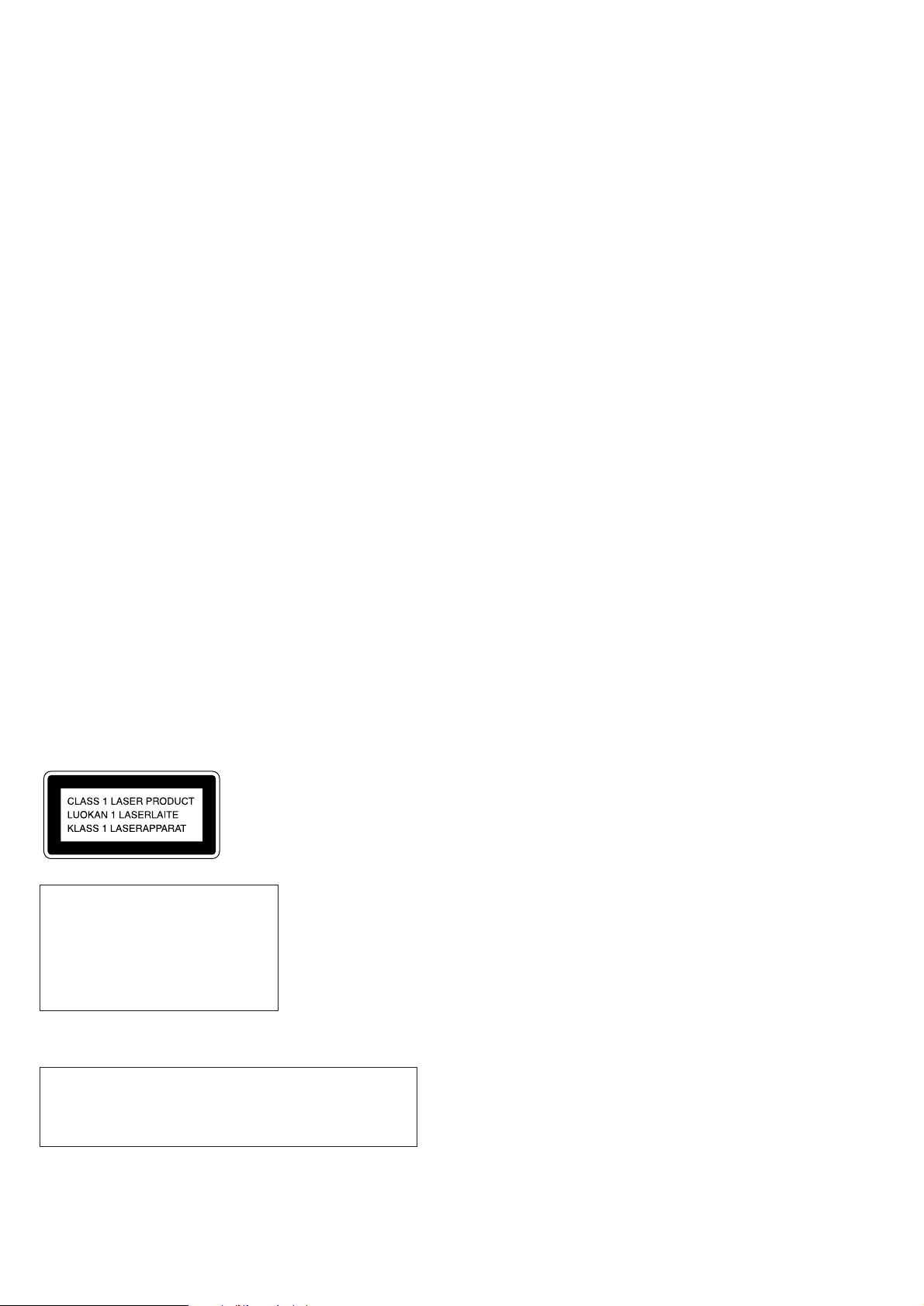
TABLE OF CONTENTS
Specifications ........................................................................... 1
1. SERVICING NOTE.......................................................... 3
2. GENERAL
Location and Function of Controls .................................... 6
3. DISASSEMBLY ............................................................... 8
4. TEST MODE ...................................................................11
5. ELECTRICAL ADJUSTMENTS ................................. 14
6. DIAGRAMS
6-1. IC Pin Description .................................................... 16
6-2. Block Diagram.......................................................... 18
6-3. Printed Wiring Board................................................ 21
6-4. Schematic Diagram................................................... 25
7. EXPLODED VIEWS
7-1. Panel Section ............................................................ 32
7-2. Mechanism Deck Section (MT-MZEP10-129) ........ 33
Ver 1.1 1998.05
8. ELECTRICAL PARTS LIST ........................................ 34
This Mini Disc player is classified as a CLASS 1 LASER product.
The CLASS 1 LASER
PRODUCT label is located on
the bottom exterior.
IN NO EVENT SHALL SELLER BE
LIABLE FOR ANY DIRECT,
INCIDENT AL OR CONSEQUENTIAL
DAMAGES OF ANY NATURE, OR
LOSSES OR EXPENSES RESULTING
FROM ANY DEFECTIVE PRODUCT
OR THE USE OF ANY PRODUCT.
“MD WALKMAN” is a trademark of Sony
Corporation.
CAUTION
Use of controls or adjustments or performance of procedures
other than those specified herein may result in hazardous
radiation exposure.
Flexible Circuit Board Repairing
• Keep the temperature of the soldering iron around 270°C during
repairing.
• Do not touch the soldering iron on the same conductor of the
circuit board (within 3 times).
• Be careful not to apply force on the conductor when soldering or
unsoldering.
Notes on chip component replacement
• Never reuse a disconnected chip component.
• Notice that the minus side of a tantalum capacitor may be damaged by heat.
SAFETY-RELATED COMPONENT WARNING!!
COMPONENTS IDENTIFIED BY MARK ! OR DO TTED LINE WITH
MARK ! ON THE SCHEMATIC DIAGRAMS AND IN THE PARTS
LIST ARE CRITICAL TO SAFE OPERATION.
REPLACE THESE COMPONENTS WITH SONY PARTS WHOSE
PART NUMBERS APPEAR AS SHOWN IN THIS MANUAL OR IN
SUPPLEMENTS PUBLISHED BY SONY.
ATTENTION AU COMPOSANT AYANT RAPPORT
À LA SÉCURITÉ!
LES COMPOSANTS IDENTIFIÉS P AR UNE MARQUE ! SUR LES
DIAGRAMMES SCHÉMATIQUES ET LA LISTE DES PIÈCES
SONT CRITIQUES POUR LA SÉCURITÉ DE FONCTIONNEMENT .
NE REMPLACER CES COMPOSANTS QUE PAR DES PIÈCES
SONY DONT LES NUMÉROS SONT DONNÉS DANS CE MANUEL
OU DANS LES SUPPLÉMENTS PUBLIÉS PAR SONY.
– 2 –
Page 3
SECTION 1
y
SERVICING NOTE
When repairing this device with the power on, if you remove the main board, this device stops working.
In this case, you work without the device stopping by fastening the hook of the Open/Close detection switch (S801) with tape.
Chassis ass
Tape
Main board
Open/Close switch (S801)
– 3 –
Page 4
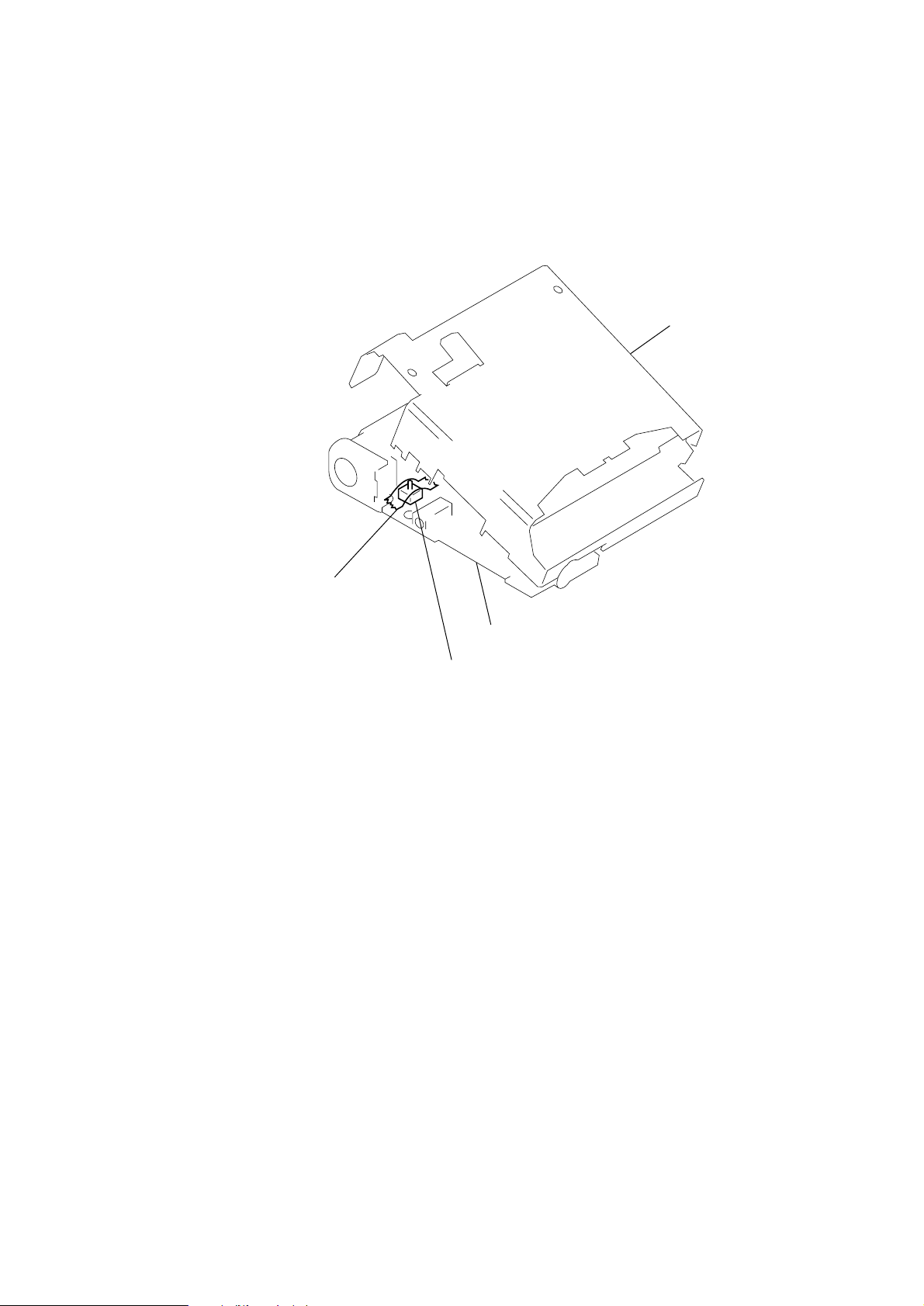
OPERATIONS OF MECHANISM (MZ-EP11)
When loading a disc
The disc shutter 1 opens when a disc is loaded. (Fig. 1)
≥
When a disc is loaded, the open lever 2 moves in arrow direction
a, and the holder assembly 3 lock is released. (Fig. 1 to 3)
≥
The slider 4 slides in arrow direction b, and the holder assembly
3 moves down to the chassis assembly (below). (Fig. 4)
≥
The OPEN/CLOSE SW (S801) is turned ON by the connection
lever linked. (Fig. 1)
≥
The wakeup mode is set and the power circuit starts operating.
Disc shutter
OPEN/CLOSE SW (S801)
1
Insert the Mini Disc
ON
(Fig. 1)
Open lever
Slider
2
b
4
Lock
Relesse
Open lever
Insert the Mini Disc
Open lever
2
2
(Fig. 2)
Slider
Descends to chassis side (below)
b
4
(Fig. 4)
Slider
Holder assembly
– 4 –
4
(Fig. 3)
3
Page 5
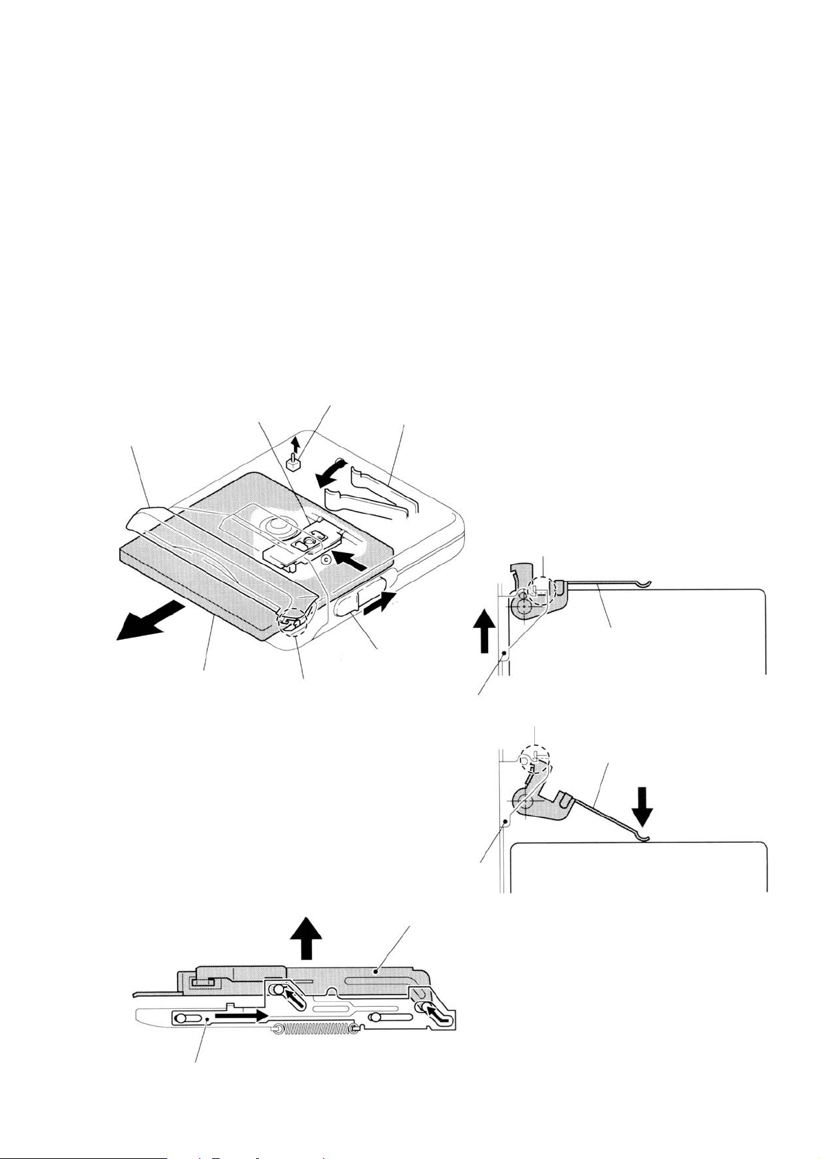
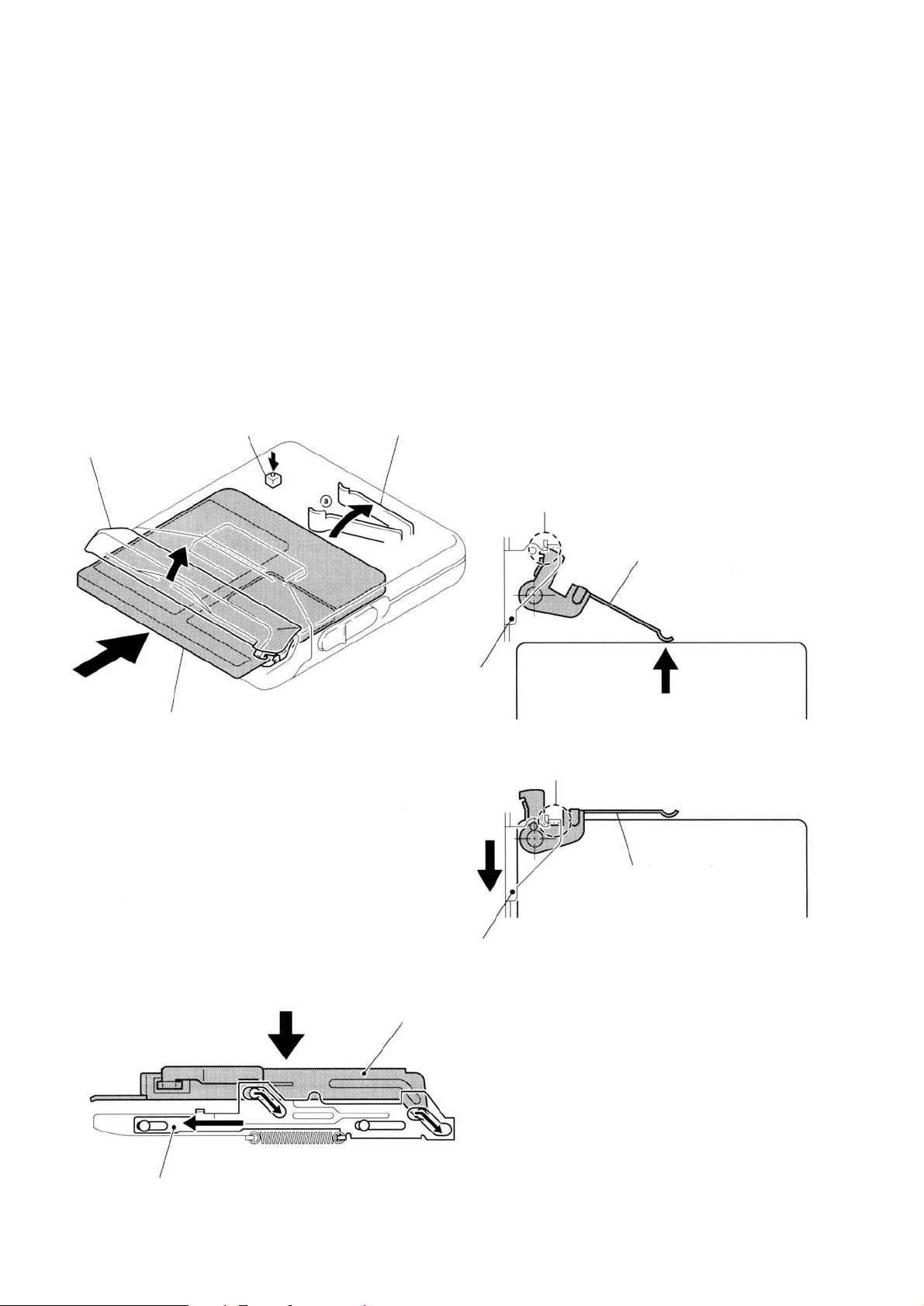
When removing the disc
When the open knob 1 is slid in arrow direction a, and the open
slider 2 lock is released, the disc shutter 3 opens. (Fig. 5)
≥
The slider 4 slides in arrow direction b, and the holder assembly
5 moves up to the upper panel (above). (Fig. 6, Fig. 8)
≥
The OPEN/CLOSE SW (S801) is turned OFF by the connection
lever linked. (Fig. 5)
≥
The optical pick-up block 6 moves to the inner circumference c.
(Fig. 5)
≥
The disc 7 is pushed by the open lever 8, and ejected out from
the holder assembly 5. (Fig. 7)
≥
The sleep mode is set and the power supply stops.
OPEN/CLOSE SW (S801)
Disc shutter
Optical pick-up block
3
6
Open lever
OFF
8
Disc is ejscted
Open knob
7
Open Slider
(Release)
2
(Fig. 5)
Moves up to the upper panel (above)
a
1
Slider
Slider
Holder assembly
b
5
4
4
Relesse
Lock
Open lever
Open lever
Disc is ejscted
8
8
(Fig. 6)
7
(Fig. 7)
Slider
4
b
(Fig. 8)
– 5 –
Page 6
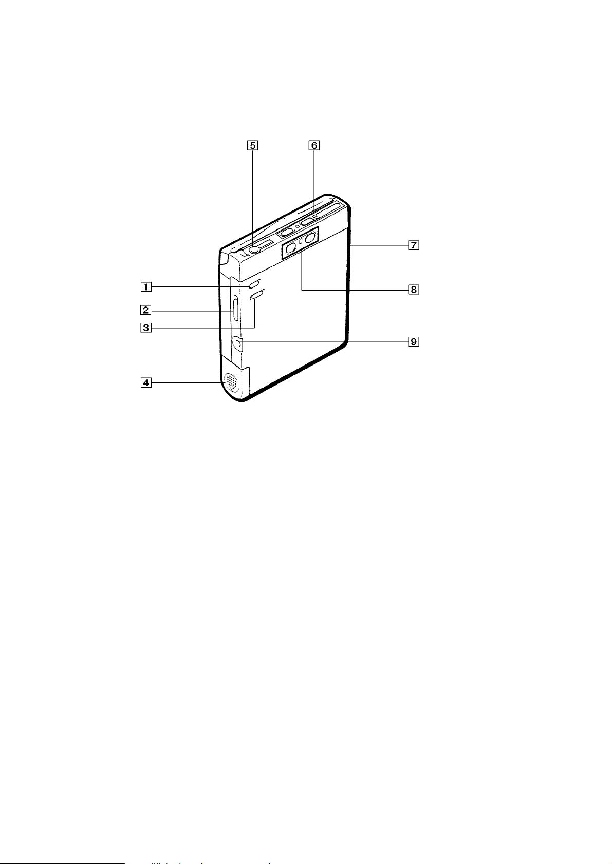
LOCATION AND FUNCTION OF CONTROLS
r
Main Unit
SECTION 2
GENERAL
1 AVLS switch
2 HOLD switch
3 DIGITAL MEGA BASS switch
4 Battery compartment
5 2 / REMOTE jack
6 MD operate buttons
( (play) button
=, +button
p button
7 EJECT knob
8 VOLUME +, – buttons
9 DC IN 1.5V jack
– 6 –
Page 7
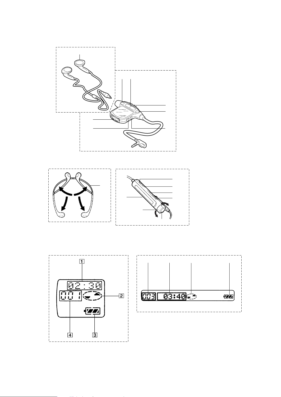
Ver 1.1 1998.05
r
Headphones with Remote Control
Except US model
1
6
7
23
Tourist model
4
5
8
1 Headphones
2 P (pause) button
3 (/+, = buttons
4 HOLD switch
5 p (stop) button
6 VOL +, – buttons
7 DISPLAY button
8 PLAYMODE button
US model
r
Display windows (Remote Control)
Tourist model
1
Except T ourist model
6
3
Except Tourist model
4
5
1
7
8
2
4
1 Headphones
2 P (pause) button
3 (/+, = control
4 HOLD switch
5 p (stop) button
6 VOL +, – buttons
7 DISPLAY button
8 PLAYMODE button
23
1 Character display
2 Disc revolve indicator
3 Battery condition indicator
4 Track number display
– 7 –
Page 8
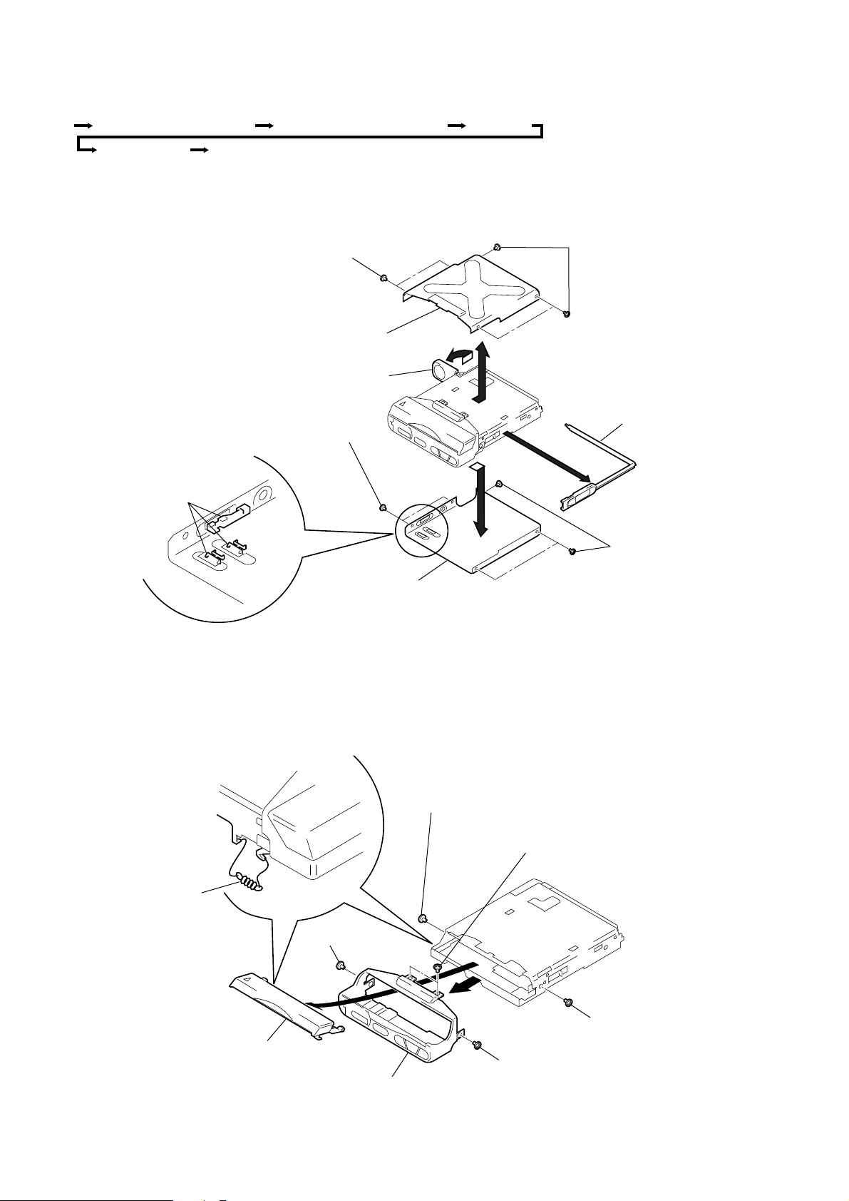
SECTION 3
)
)
DISASSEMBLY
r
The equipment can be removed using the following procedure.
Set
Panel (X) upper, Bottom panel Plate (Control) assy, ornamental Main board
Mechanism deck
Optical pick-up
Note : Follow the disassembly procedure in the numerical order given.
3-1. PANEL (X) UPPER, BOTTOM PANEL REMOVAL
2
Screws
(M1.4 precision pan)
Panel (X) upper
Lid, battery case
5
Screws
(M1.4 precision pan)
* Caution during assembly
Align the MEGA BASS knob,
AVLS knob and the HOLD knob
position with the switch
on the Main board.
Bottom panel
1
4
6
3
Screws
(M1.4 precision pan)
7
Stripe (A) assy,
Ornamental
5
Screws
(M1.4 precision pan
3-2. PLATE (CONTROL) ASSY, ORNAMENTAL REMOVAL
1
Spring (Shutter),
Tension
4
Screw (step)
3
Shutter
Plate (Control) assy,
ornamental
2
Screw
(M1.4 precision pan)
5
Screws
(M1.4 precision pan)
6
4
Screw (step)
2
Screw
(M1.4 precision pan
– 8 –
Page 9

3-3. MAIN BOARD REMOVAL
r
)
2
Screws
(M1.4 toothed lock)
Main board
5
OP flexible board
(Main board CN501)
4
Switch unit
(Main board CN802)
1
Screw (1.7 tapping)
2
Screws
(M1.4 toothed lock)
3
Remove solder
3-4. MECHANISM DECK REMOVAL
6
7
CLV flexible board
(Main board CN551)
Mechanism deck
4
Damper
Battery flexible
board
3
Remove solde
1
Screws
(M1.4 precision pan
4
Dampers
5
Chassis (B) assy
3
Screws
(M1.4 precision pan)
– 9 –
Case, battery
2
Chassis assy
Page 10

3-5. OPTICAL PICK-UP REMOVAL
)
Optical Pick-up
2
1
Screw ( precision)
3-6. HOLDER ASSY REMOVAL
3
Holder assy
1
Washer (0.8–2.5
2
Spring (holder)
– 10 –
Chassis assy
Page 11

” key
” key
p key
p key
p key
p key
VOL
+ key
VOL
– key
(Start ?)
Overall
adjustment
mode (Auto?)
Adjustment
mode
(Manu ?)
Servo mode
0 0 0
Audio mode
1 0 0
Servo mode
3 0 0
+, – keys
+, – keys
+, – keys
Display when test mode
is set
Displays of the LCD on the remote commander
are shown in parentheses.
Ver 1.1 1998.05
SECTION 4
TEST MODE
Outline
• In this set, overall adjustment mode is made available by entering test mode to perform automatic adjustment of CD and MO.
In the overall adjustment mode, the disc is determined whether
it is CD or MO and adjustments are performed in sequence. If a
fault is found, the location of the fault is displayed. Also, in servo
mode, each adjustment can be automatically made.
Setting the Test Mode
To enter the test mode, two methods are available :
1. Entering method with key input.
Turn on the HOLD switch on the set. While holding down the p
key on the set, press the following remote commander keys in
the following order :
+ n + n = n = n + n = n + n
=n P n P
2. Entering method by shorting the test point
Solder bridge the test point TAP801 (TEST) on the main board
(connect IC801 pin #™ to GND), and turn on the POWER.
[MAIN BOARD] (Conductor side)
Test mode
Short : Test mode
( )
Open : Normal mode
Configuration of Test Mode
The test mode has the configuration given below.
Servo Mode
• Set the test mode, press the VOLUME – key and use the ( key
to set the servo mode.
• When the servo mode is set, use the + key and the = key
to move the optical pick-up to the outer circumference and to
the inner circumference respectively.
• When entering another mode, refer to the configuration of test
mode.
1. Structure of Servo Mode
Servo mode
0 0 0
” key
Releasing the Test Mode
1. When test mode was entered with key input, turn off the POWER.
2. When test mode was entered by shorting the test point, turn off
the POWER and open the solder bridge of TAP801 (TEST
MODE) on the main board.
Operation of Setting on Test Mode
When the test mode is set, the LCD displays the following :
• ROM version display to all LEDs ON to all LEDs OFF and so
on.
These operations are repeated.
• When the PLAY MODE key is pressed and hold down, the display at that time is held so that display can be checked.
V2. 00
LCD on remote commander
ROM version display
p key
p key
1
(See page 12.)
Offset adjustment
0 1 0
p key
+, – keys+, – keys
Laser power
adjustment
0 2 0
p key
23
*1 Repeatedly press ” key
” key
011 to 013
*1
” key
” key
021 to 024
*1
” key
to change the mode.
(Refer to the following list
for a description of each
mode.)
– 11 –
Page 12

Ver 1.1 1998.05
(See page 11.)
1
p key
p key
p key
23
MO adjustment
0 3 0
p key
+, – keys
Low reflection
CD adjustment
0 4 0
p key
+, – keys
CD adjustment
0 5 0
p key
+, – keys
” key
” key
” key
031 to 039
*1
” key
041 to 048
*1
” key
051 to 058
*1
” key
2. Description of Each Mode
010 Offset adjustment
Mode Description
011 FE offset
012 TE offset
013 All servo ON
020 Laser power adjustment
Mode Description
021 MO power A
022 MO power E
023 CDL power
024 CD power
030 MO adjustment
Mode Description
031 MO EF balance
032 MO EF gain
033 MO ABCD gain
034 MO focus gain
035 MO tracking gain
036 MO RF gain
037 MO ADIP gain
038 MO focus bias E
039 CD focus bias A
p key
p key
p key
Sled movement
0 6 0
p key
+, – keys
Automatic
adjustment
0 7 0
p key
+, – keys
NV relation
0 9 0
p key
+, – keys
Retern the Offset
adjustment (0 1 0)
” key
061 , 062
*1
” key
” key
071, 072,
073, 074
*1
” key
” key
091, 092,
093
*1
” key
*1 : Repeatedly press ” key
to change the mode.
(Refer to the following list
for a description of each
mode.)
040 Lower reflection CD adjustment
Mode Description
041 Lower reflection CD EF balance
042 Lower reflection CD EF gain
043 Lower reflection CD ABCD gain
044 Lower reflection CD focus gain
045 Lower reflection CD tracking gain
046 Lower reflection CD RF offset
047 Lower reflection CD RF gain
048 Lower reflection CD focus bias
050 CD adjustment
Mode Description
051 CD EF balance
052 CD EF gain
053 CD ABCD gain
054 CD focus gain
055 CD tracking gain
056 CD RF offset
057 CD RF gain
058 CD focus bias
– 12 –
Page 13

060 Seld movement
Audio mode
1 0 0
Audio playback test
1 1 0
1kHz 0dB L/R
1 1 1
Infinity Zero
1 1 2
–12dB
–
–12dB
–12dB
–20dB
–20dB
–20dB
–20dB
–40dB
1kHz 0dB L
1 1 3
1kHz 0dB R
1 1 4
1kHz 0dB L/R
1 1 5
20Hz 0dB L/R
1 1 6
20kHz 0dB L/R
1 1 7
100kHz De-Emphasis
1 1 8
100kHz 0dB L/R
1 1 9
headphones
output
p key
p key
” key
” key
” key
p key
” key
p key
” key
p key
” key
p key
” key
p key
” key
p key
” key
p key
” key
p key
” key
Mode Description
061 Seld in
062 Seld out 5
070 Automatic adjustment
Mode Description
071 Focus search
072 Access 32
073 ADER check
074 Tracking sensitivity adjust
090 NV relation
Mode Description
091 NV clear
092 Power OFF
093 Function code change
Audio Mode
• Enter the test mode and press the VOLUME – key. Then, press
the ( key and the VOLUME + key in this turn to enter audio
mode.
• When entering another mode, refer to the configuration of test
mode.
1. Structure of Audio Mode
• The mode No. 111 is for S/N and crosstalk. The mode No. 115 is
for distortion factor and frequency characteristics.
• When the VOLUME +/– keys is pressed in any mode, the volume of the headphones is changed (increased/decreased) in units
of one step. When the + / = keys is pressed, the volume of
the headphones is maximized/minimized.
• For the volume value, any changed value remains as it is basically.
However, when the volume is switched from 114 to 115 or 118
to 119, it returns the default value.
– 13 –
Page 14

SECTION 5
ELECTRICAL ADJUSTMENTS
Power Mode
• Enter the test mode and press the VOLUME – key. Then, press
the ( key and the VOLUME – key in this turn to enter power
mode.
• When entering another mode, refer to the configuration of test
mode.
1. Structure of Power Mode
Power mode
3 0 0
p key
” key
UNREG check
31 0
p key
” key
Power OFF
3 1 1
” key
Overall Adjustment Mode
• Enter the test mode and press the VOLUME + key to enter overall adjustment mode.
• When entering another mode, refer to the configuration of test
mode.
• When the overall adjustment mode is entered, the LCD on the
remote commander display the following :
Auto ?
000
1. Structure of Overall Adjustment Mode
Overall
adjustment
mode
Auto?
” key
Notes for Adjustment
• In this set, automatic adjustment of CD and MO can be performed by entering the test mode.
• Adjustments are performed in the overall adjustment mode. If
an item is determined as NG, the item is readjusted in servo
mode.
Adjustment Method in Overall Adjustment Mode
1. Enter the test mode and press the VOLUME + key to enter overall adjustment mode.
2. Insert the CD test disc (TGYS-1) or SONY MO disc (recorded)
commercially availble.
3. Press the ( key twice. The disc is determined whether it is CD
or MO and each adjustment mode is set. Automatic adjustments
are performed in the order of the items listed below.
• In CD Automatic adjustment Mode
No. Mode Description
1 061 Sled in
2 071 Focus search
3 062 Sled out 5
4 051 CD EF balance
5 052 CD EF gain
6 051 CD EF balance
7 053 CD ABCD gain
8 054 CD foucus gain
9 055 CD tracking gain
10 056 CD RF offset
11 057 CD RF gain
12 056 CD RF offset
13 058 CD Focus bias
Start ?
” key (to discriminate between CD and MO)
CD automatic
adjustment
MO automatic
adjustment
OK
NG
OK
NG
p key
p key
p key
p key
Adjustment
mode
Manu ?
– 14 –
Page 15

• In MO Automatic adjustment Mode
No. Mode Description
1 061 Sled in
2 071 Focus search
3 062 Sled out
4 031 MO EF balance
5 032 MO EF gain
6 031 MO EF balance
7 033 MO ABCD gain
8 034 MO focus gain
9 035 MO tracking gain
10 036 MO RF gain
11 037 MO ADIP gain
12 038 MO focus bias E
13 039 MO focus bias A
14 073 ADER check
15 061 Sled in
16 071 Focus search
17 041 Low reflection CD EF balance
18 042 Low reflection CD EF gain
19 041 Low reflection CD EF balance
20 043 Low reflection CD ABCD gain
21 044 Low reflection CD focus gain
22 045 Low reflection CD tracking gain
23 046 Low reflection CD RF offset
24 047 Low reflection CD RF gain
Adjustment in Servo Mode Method
1. When each adjustment mode is set according to the structure of
servo mode, the lower two digits of the mode No. and the adjustment value written in EEPROM are displayed and lit on the LCD
on the remote commander.
13
052
Adjustment value (lit)
Mode No.
2. When the P key is pressed, the following display appears and
the automatic adjustment is performed.
13
052
Note) Although the VOLUME +/– keys can be used to change the
Adjustment value (flashing)
adjustment value to any value, they should not be used whenever possible.
3. When the automatic adjustment is completed, the flashing adjustment value is lit.
13
052
Adjustment value (lit)
* Remote commander display during automatic adjustment
12
057
Adjustment value (flashing)
Mode No. under adjustment
4. If result of automatic adjustment is OK, the following display
appears.
End-OK
058
5. If result of automatic adjustment is NG, the following display
appears.
NG 04
051
NG mode No.
* If NG, enter servo mode to perform automatic adjustment of the
item determined as NG.
– 15 –
Page 16

SECTION 6
DIAGRAMS
6-1. IC PIN DESCRIPTION
IC801 RU6715MF-0004 (SYSTEM CONTROL)
Pin No. Pin Name I/O Pin Description
1 CHG MON – Not used (Fixed at “L” ).
2 UREG MON I Unreg voltage monitor input.
3 VTEMP I Temperature sensor input.
4 VREF I Reference voltage monitor input.
5 PLAY KEY I Set PLAY key input.
6 OPEN/CLS SW I OPEN/CLOSE switch input.
7 RMC KEY I Remote commander key input.
8 SET KEY I Set key input.
9 XRESET I Systen reset input (At reset : “L” ).
10 AVDD – A/D converter power supply.
11 AVSS – A/D converter GND.
12 TYPE 0 I (Fixed at “L” ).
13 TYPE 1 I (Fixed at “L” ).
14 HOLD SW I Set HOLD switch input.
15 MODEL I (Fixed at “L” ).
16 TYPE 2 I (Fixed at “L” ).
17 VREG CON O 2.5V voltage on/off switch.
18 XWK CLR O Power IC wakeup factor latch clear outpu and motor driver IC control signal outpt.
19 SLEEP O System sleep ouput.
20 MCK I Master clock input.
21 NC – Not used (Open).
22 VDD – Digital power supply.
23 VSS – Digital Ground.
24 NC – Not used (Open).
25 VSS – Digital Ground.
26 UREG CHK CON O Not used (Open).
27 DSP SINT I Interrupt input from DSP.
28 DBB OFF I DBB switch.
29 AVLS SW I Set AVLS switch input.
30 OPR LED O LED drive.
31 NC – Not used (Open).
32 ADJUST I “Normally, Test mode select input (“L” : Test mode)
33 NC – Not used (Open).
34 SBUS CLK O SBB serial clock output.
35 SBUS DATA O SBB serial data output.
36 FR CAP I Free-run counter capture input (Not used).
37 SLD 1 MON I Sled servo timing signal input.
38 SLD 2 MON I Sled servo timing signal input.
39 CLV VCON O Spindle servo drive voltage control output.
40 V28-CON O Power voltage correction control output.
41 APC REF O Laser power control output.
42 CLV U MON I Spindle servo timing signal input.
43 CLV V MON I Spindle servo timing signal input.
44 CLV W MON I Spindle servo timing signal input.
45 CL V U CON O Spindle servo drive signal output.
– 16 –
Page 17

Pin No. Pin Name I/O Pin Description
46 CLV V CON O Spindle servo drive signal output.
47 CLV W CON O Spindle servo drive signal output.
48 NC – Not used (Open).
49 FR TRG – Free-run counter capture output (Not used).
50 VDD – Digital power supply.
51 VPP – Power for on board light.
52 VSS – Digital ground.
53 SLD 1R CON O Gate array control signal output.
54 SLD 1F CON O Gate array control signal output.
55 SLD 2R CON O Gate array control signal output.
56 SLD 2F CON O Gate array control signal output.
57 SLD DLY4 O Gate array control signal output.
58 SLD DLY5 O Gate array control signal output.
59 SLD DLY6 O Gate array control signal output.
60 SLD MODE O Gate array control signal output.
61 SPCK – Not used (Open).
62 RMC DTCLK I/O TSB serial data input/output.
63 – 65 NC – Not used (Open).
66 SLD DIR O Gate array control output.
67 SLD VCON O Sled servo outer voltage control output.
68 SLD PWR-UP O Baypass transistor control output for sled drive power supply.
69 HP MUTE O Headphone amplifier mute output.
70 HP STBY O Headphone amplifier standby output.
71 RMC SEL O Not used (Open).
72 NV D0 O Serial data signal output for NVRAM.
73 NV D1 I Serial data signal input from NVRAM.
74 NV CLK O Serial clock signal output for NVRAM.
75 NV CS1 O Chip select signal output for NVRAM.
76 VDD – Digital power supply.
77 – 79 LCD VL2 – 0 I LCD drive level power supply (Ground).
80 VSS – Digital ground.
81 – 87 NC – Not used (Open).
88 – 96 LCD SEG0 – 8 – Not used (Open).
97 – 100 LCD COM0 – 3 – Not used (Open).
MZ-EP11
6-2. BLOCK DIAGRAM
– 17 – – 18 – – 20 –– 19 –
• Signal path.
J : PLAY
Page 18

Ver 1.2
Page 19

p
p
p
Ver 1.1 1998.05
MZ-EP11
6-4. SCHEMATIC DIAGRAM
r
Refer to page 29 for IC Block Diagrams.
r
WA VEFORMS
PLAY MODE
1
IC501 #¶ RF OUT
TIME/DIV : 20 nsec
2
VOLT/DIV : 0.1V AC
16.0 MHz
IC301 5 XT1
TIME/DIV : 50 nsec
3
VOL T/DIV : 0.5V AC
TIME/DIV : 0.5µ sec
VOLT/DIV : 0.5V
1.0 Vp-
0.4 Vp-
0.9 Vp-
59.8 msec
IC601 $• X1
Note:
• All capacitors are in µF unless otherwise noted. pF: µµF
50 WV or less are not indicated except for electrolytics
and tantalums.
• All resistors are in Ω and 1/
specified.
Note: Note:
The components identi- Les composants identifiés
fied by mark ! or dotted par une marque ! sont criline with mark ! are cri- tiques pour la sécurité.
tical for safety. Ne les remplacer que par
Replace only with part une piéce portant le
number specified. numéro spécifié.
• U : B+ Line.
• Power voltage is dc 1.5V and fed with regulated dc power
supply from external power voltage jack. (J901)
• Voltages and waveforms are dc with respect to ground
under no-signal conditions.
no mark : PLAY
• Voltages are taken with a VOM (Input impedance 10 MΩ).
Voltage variations may be noted due to normal production tolerances.
• Waveforms are taken with a oscilloscope.
Voltage variations may be noted due to normal production tolerances.
• Circled numbers refer to waveforms.
• Signal path.
– 25 – – 26 – – 28 –– 27 –
J : PLA Y
4
W or less unless otherwise
Page 20

NOTE :
• -XX, -X mean standardized parts, so they
may have some difference from the original
one.
• Items marked “ * ”are not stocked since they
are seldom required for routine service. Some
delay should be anticipated when ordering
these items.
7-1. PANEL SECTION
SECTION 7
EXPLODED VIEWS
• The mechanical parts with no reference
number in the exploded views are not
supplied.
• Hardware (# mark) list and accessories and
packing materials are given in the last of this
parts list.
• Abbreviation
JE : Tourist
1
1
Ver 1.2
The components identified by mark !
or dotted line with mark ! are critical
for safety.
Replace only with part number specified.
Les composants identifiés par une
marque ! sont critiques pour la sécurité.
Ne les remplacer que par une pièce
portant le numéro spécifié.
10
1
11
IC602 MSM51V4400-70TS-K
7
23
6
8
not
supplied
25
9
1
1
19
not supplied
12
20
13
1
14
1
15
22
18
1
16
1
23
5
24
21
not supplied
1
4
3
17
2
RAS
CAS
VDD
GND
4
23
9
A0
10
A1
11
A2
12
A3
14
A4
15
A5
16
A6
17
A7
18
A8
5
A9
13
26
TIMING
GENERATOR
COLUM
ADDRESS
BUFFERS
INTERNAL
ADDRESS
COUNTER
ROW
ADDRESS
BUFFERS
DECODERS
ON CHIP V
REFRESH
CONTROL CLOCK
ROW
DD
WORD
DRIVERS
COLUM
DECODERS
SENSE
AMPS
MEMORY
CELLS
TIMING
GENERATOR
WRITE
CLOCK
GENERATOR
I/O
SELECTOR
INPUT
BUFFERS
OUTPUT
BUFFERS
3
WE
22
OE
1
D0
2
D1
24
D2
25
D3
Ref. No. Part No. Description Remark Ref. No. Part No. Description Remark
1 4-963-883-21 SCREW (M1.4), PRECISION PAN
15 4-993-389-01 SPRING (BATTERY), COMPRESSION
2 4-993-374-11 PANEL, BOTTOM
3 4-982-398-21 KNOB (BASS BOOST)
4 4-982-397-21 KNOB (AVLS)
5 4-986-207-21 KNOB (TUN)
16 1-666-783-11 FLEXIBLE BOARD
17 X-4948-818-1 STRIP (A) ASSY, ORNAMENTAL
18 A-3293-628-A MAIN BOARD, COMPLETE (JE)
18 A-3293-828-A MAIN BOARD, COMPLETE (EXCEPT JE)
6 X-4948-817-1 PLATE (CONTROL)ASSY,ORNAMENTAL
19 7-627-455-07 SCREW +K1.4X1.4, PRECISION
7 4-993-386-01 SPRING (SHUTTER), TENSION
8 4-993-384-01 SHUTTER
9 4-993-387-01 STRIP (B), ORNAMENTAL
10 4-993-413-01 PANEL (X), UPPER
20 4-963-883-41 SCREW (M1.4), PRECISION PAN
21 3-335-797-91 SCREW (M1.4), TOOTHED LOCK
22 4-984-017-11 SCREW (1.7), TAPPING
23 4-993-385-01 SCREW, STEP
11 4-993-392-02 LID, BATTERY CASE
24 3-338-625-11 SCREW (M1.4X1.6), WASHER HEAD
12 X-4948-821-1 TERMINAL BOARD ASSY, MINUS
13 4-993-415-01 CASE, BATTERY
25 3-350-775-01 SPACER
14 X-4948-820-1 TERMINAL BOARD ASSY, PLUS
– 31 – – 32 –– 29 – – 30 –
Page 21

Ver 1.1 1998.05
7-2. MECHANISM DECK SECTION
(MT-MZEP10-129)
59
62
51
58
not
supplied
61
M901
51
57
63
M902
51
56
not supplied
64
55
51
54
53
52
71
67
57
65
66
68
69
70
51
The components identified by
mark ! or dotted line with mark
! are critical for safety.
Replace only with part number
specified.
Ref. No. Part No. Description Remark Ref. No. Part No. Description Remark
51 4-963-883-21 SCREW (M1.4), PRECISION PAN
52 X-4948-793-1 LEAD ASSY
53 4-982-555-01 GEAR (A)
54 4-965-893-01 WASHER, GEAR (A) STOPPER
55 4-982-563-01 SPRING, THRUST
56 1-666-784-11 FLEXIBLE BOARD (CLV)
57 4-993-388-01 DAMPER
58 1-475-297-11 SWITCH UNIT
* 59 X-4948-822-1 CHASSIS (B) ASSY, SET
61 3-338-645-41 WASHER (0.8-2.5)
62 X-4948-816-1 CHASSIS ASSY, SET
63 4-900-951-01 SPRING (HOLDER)
64 X-4948-792-1 HOLDER ASSY
* 65 X-4948-790-1 CHASSIS ASSY
66 4-993-253-01 SPRING (SLIDE), TENSION
67 4-993-252-01 SPRING (EJECT), TENSION
68 4-993-251-01 SHAFT, MAIN
! 69 X-4949-080-1 OPTICAL PICK-UP ASSY (ODX-1A)
70 4-982-561-11 SPRING, RACK
71 3-349-825-82 SCREW, PRECISION
M901 8-835-594-01 MOTOR, DC SSM-01C03A/J-S (SPINDLE)
M902 1-698-764-11 MOTOR, SLED (SLED)
Les composants identifiés par une
marque ! sont critiques pour
la sécurité.
Ne les remplacer que par une pièce
portant le numéro spécifié.
– 33 –
Page 22

Ver 1.1 1998.05
SECTION 8
MAIN
NOTE :
• Due to standardization, replacements in the
parts list may be different from the parts
specified in the diagrams or the components
used on the set.
• -XX, -X mean standardized parts, so they
may have some difference from the original
one.
• RESISTORS
All resistors are in ohms
METAL : Metal-film resistor
METAL OXIDE :Metal oxide-film resistor
F : nonflammable
• Items marked “ * ”are not stocked since
they are seldom required for routine service.
Some delay should be anticipated when
ordering these items.
Ref. No. Part No. Description Remark Ref. No. Part No. Description Remark
A-3293-628-A MAIN BOARD, COMPLETE (JE)
A-3293-828-A MAIN BOARD, COMPLETE (EXCEPT JE)
*********************
* 4-993-391-01 RETAINER (DC)
< CAPACITOR >
C101 1-107-812-11 TANTAL. CHIP 4.7uF 20% 6.3V
C102 1-115-585-11 TANTAL. CHIP 220uF 20% 4V
C103 1-107-826-11 CERAMIC CHIP 0.1uF 10% 16V
C201 1-107-812-11 TANTAL. CHIP 4.7uF 20% 6.3V
C202 1-115-585-11 TANTAL. CHIP 220uF 20% 4V
C203 1-107-826-11 CERAMIC CHIP 0.1uF 10% 16V
C301 1-111-253-11 TANTAL. CHIP 100uF 20% 6.3V
C302 1-162-912-11 CERAMIC CHIP 7PF 0.5PF 50V
C303 1-162-912-11 CERAMIC CHIP 7PF 0.5PF 50V
C304 1-162-970-11 CERAMIC CHIP 0.01uF 10% 25V
C305 1-117-919-11 TANTAL. CHIP 10uF 6.3V
C307 1-117-919-11 TANTAL. CHIP 10uF 6.3V
C308 1-117-919-11 TANTAL. CHIP 10uF 6.3V
C309 1-162-970-11 CERAMIC CHIP 0.01uF 10% 25V
C311 1-109-982-11 CERAMIC CHIP 1uF 10% 10V
C312 1-113-600-11 TANTAL. CHIP 2.2uF 20% 6.3V
C314 1-104-929-11 TANTAL. CHIP 22uF 20% 6.3V
C315 1-109-982-11 CERAMIC CHIP 1uF 10% 10V
C316 1-109-888-11 TANTAL. CHIP 3.3uF 20% 6.3V
C317 1-109-982-11 CERAMIC CHIP 1uF 10% 10V
C319 1-162-970-11 CERAMIC CHIP 0.01uF 10% 25V
C320 1-107-826-11 CERAMIC CHIP 0.1uF 10% 16V
C322 1-162-964-11 CERAMIC CHIP 0.001uF 10% 50V
C324 1-107-826-11 CERAMIC CHIP 0.1uF 10% 16V
C327 1-162-964-11 CERAMIC CHIP 0.001uF 10% 50V
C328 1-162-964-11 CERAMIC CHIP 0.001uF 10% 50V
C329 1-162-964-11 CERAMIC CHIP 0.001uF 10% 50V
C501 1-162-964-11 CERAMIC CHIP 0.001uF 10% 50V
C502 1-107-826-11 CERAMIC CHIP 0.1uF 10% 16V
C503 1-162-919-11 CERAMIC CHIP 22PF 5% 50V
C504 1-162-919-11 CERAMIC CHIP 22PF 5% 50V
C505 1-162-917-11 CERAMIC CHIP 15PF 5% 50V
C506 1-164-227-11 CERAMIC CHIP 0.022uF 10% 25V
C507 1-162-962-11 CERAMIC CHIP 470PF 10% 50V
C508 1-107-826-11 CERAMIC CHIP 0.1uF 10% 16V
C509 1-117-720-11 CERAMIC CHIP 4.7uF 10V
ELECTRICAL PARTS LIST
• SEMICONDUCTORS
In each case, u : µ , for example :
uA.... : µ A.... , uPA.... : µ PA....
uPB.... : µ PB.... , uPC.... : µ PC....
uPD.... : µ PD....
• CAPACIT ORS
uF : µ F
• COILS
uH : µ H
• Abbreviation
FR : French
JE : Tourist
C510 1-164-227-11 CERAMIC CHIP 0.022uF 10% 25V
C511 1-162-970-11 CERAMIC CHIP 0.01uF 10% 25V
C513 1-107-826-11 CERAMIC CHIP 0.1uF 10% 16V
C514 1-107-826-11 CERAMIC CHIP 0.1uF 10% 16V
C515 1-162-908-11 CERAMIC CHIP 3PF 0.25PF 50V
C516 1-162-910-11 CERAMIC CHIP 5PF 0.25PF 50V
C551 1-162-964-11 CERAMIC CHIP 0.001uF 10% 50V
C552 1-162-964-11 CERAMIC CHIP 0.001uF 10% 50V
C553 1-117-720-11 CERAMIC CHIP 4.7uF 10V
C554 1-117-720-11 CERAMIC CHIP 4.7uF 10V
C555 1-107-765-11 TANTAL. CHIP 3.3uF 20% 16V
C556 1-107-765-11 TANTAL. CHIP 3.3uF 20% 16V
C557 1-135-238-21 TANTAL. CHIP 6.8uF 20% 10V
C558 1-135-238-21 TANTAL. CHIP 6.8uF 20% 10V
C559 1-117-720-11 CERAMIC CHIP 4.7uF 10V
C560 1-117-370-11 CERAMIC CHIP 10uF 10V
C561 1-117-370-11 CERAMIC CHIP 10uF 10V
C564 1-115-566-11 CERAMIC CHIP 4.7uF 10% 10V
C565 1-115-566-11 CERAMIC CHIP 4.7uF 10% 10V
C566 1-115-566-11 CERAMIC CHIP 4.7uF 10% 10V
C567 1-109-982-11 CERAMIC CHIP 1uF 10% 10V
C601 1-164-156-11 CERAMIC CHIP 0.1uF 25V
C602 1-117-720-11 CERAMIC CHIP 4.7uF 10V
C604 1-164-156-11 CERAMIC CHIP 0.1uF 25V
C605 1-164-156-11 CERAMIC CHIP 0.1uF 25V
C606 1-164-156-11 CERAMIC CHIP 0.1uF 25V
C607 1-162-970-11 CERAMIC CHIP 0.01uF 10% 25V
C608 1-162-970-11 CERAMIC CHIP 0.01uF 10% 25V
C610 1-162-970-11 CERAMIC CHIP 0.01uF 10% 25V
C611 1-164-156-11 CERAMIC CHIP 0.1uF 25V
C802 1-164-156-11 CERAMIC CHIP 0.1uF 25V
C803 1-164-156-11 CERAMIC CHIP 0.1uF 25V
C805 1-162-970-11 CERAMIC CHIP 0.01uF 10% 25V
C806 1-162-964-11 CERAMIC CHIP 0.001uF 10% 50V
C807 1-164-156-11 CERAMIC CHIP 0.1uF 25V
C808 1-164-227-11 CERAMIC CHIP 0.022uF 10% 25V
C809 1-162-964-11 CERAMIC CHIP 0.001uF 10% 50V
C811 1-162-970-11 CERAMIC CHIP 0.01uF 10% 25V
C812 1-162-970-11 CERAMIC CHIP 0.01uF 10% 25V
C813 1-162-970-11 CERAMIC CHIP 0.01uF 10% 25V
C901 1-162-964-11 CERAMIC CHIP 0.001uF 10% 50V
C902 1-162-970-11 CERAMIC CHIP 0.01uF 10% 25V
C903 1-107-826-11 CERAMIC CHIP 0.1uF 10% 16V
The components identified by mark !
or dotted line with mark ! are critical
for safety.
Replace only with part number specified.
Les composants identifiés par une
marque ! sont critiques pour la sécurité.
Ne les remplacer que par une pièce
portant le numéro spécifié.
When indicating parts by reference number, please include the board.
– 34 –
Page 23

MAIN
Ref. No. Part No. Description Remark Ref. No. Part No. Description Remark
C905 1-107-826-11 CERAMIC CHIP 0.1uF 10% 16V
< COIL >
C906 1-107-826-11 CERAMIC CHIP 0.1uF 10% 16V
C907 1-107-826-11 CERAMIC CHIP 0.1uF 10% 16V
C908 1-107-765-11 TANTAL. CHIP 3.3uF 20% 16V
C909 1-117-920-11 TANTAL. CHIP 10uF 6.3V
C910 1-162-970-11 CERAMIC CHIP 0.01uF 10% 25V
C911 1-117-232-11 TANTALUM 22uF 20% 4V
C912 1-162-970-11 CERAMIC CHIP 0.01uF 10% 25V
C913 1-109-982-11 CERAMIC CHIP 1uF 10% 10V
C914 1-124-576-11 ELECT 220uF 20% 4V
C915 1-109-982-11 CERAMIC CHIP 1uF 10% 10V
C916 1-117-920-11 TANTAL. CHIP 10uF 6.3V
C917 1-162-964-11 CERAMIC CHIP 0.001uF 10% 50V
C918 1-107-826-11 CERAMIC CHIP 0.1uF 10% 16V
C919 1-107-826-11 CERAMIC CHIP 0.1uF 10% 16V
C920 1-107-826-11 CERAMIC CHIP 0.1uF 10% 16V
< CONNECTOR >
CN501 1-573-360-21 CONNECTOR, FFC/FPC 20P
CN551 1-573-917-11 CONNECTOR, FFC/FPC (ZIF) 8P
CN802 1-778-711-11 CONNECTOR, FFC/FPC (ZIF) 5P
< DIODE >
D101 8-719-017-58 DIODE MA8068
D201 8-719-017-58 DIODE MA8068
D301 8-719-066-17 DIODE FTZ6.8E-T148
D303 8-719-017-58 DIODE MA8068
D304 8-719-017-58 DIODE MA8068
L301 1-414-754-11 INDUCTOR 10uH
L502 1-414-754-11 INDUCTOR 10uH
L551 1-412-031-11 INDUCTOR CHIP 47uH
L552 1-412-031-11 INDUCTOR CHIP 47uH
L553 1-414-400-11 INDUCTOR 22uH
L554 1-414-400-11 INDUCTOR 22uH
L555 1-412-031-11 INDUCTOR CHIP 47uH
L556 1-414-754-11 INDUCTOR 10uH
L601 1-414-754-11 INDUCTOR 10uH
L901 1-412-031-11 INDUCTOR CHIP 47uH
L902 1-411-804-21 COIL, CHOKE 10uH
L903 1-414-754-11 INDUCTOR 10uH
< TRANSISTOR >
Q501 8-729-922-10 TRANSISTOR 2SA1577-QR
Q551 8-729-904-87 TRANSISTOR 2SB1197K-R
Q552 8-729-929-12 TRANSISTOR DTC143ZE-TL
< RESISTOR >
R101 1-216-837-11 METAL CHIP 22K 5% 1/16W
R102 1-216-831-11 METAL CHIP 6.8K 5% 1/16W
R105 1-216-829-11 METAL CHIP 4.7K 5% 1/16W
R201 1-216-837-11 METAL CHIP 22K 5% 1/16W
R202 1-216-831-11 METAL CHIP 6.8K 5% 1/16W
R205 1-216-829-11 METAL CHIP 4.7K 5% 1/16W
R301 1-216-845-11 METAL CHIP 100K 5% 1/16W
R302 1-216-845-11 METAL CHIP 100K 5% 1/16W
D801 8-719-052-72 LED CL-220HR-C (OPERATE)
D901 8-719-421-27 DIODE MA728
D902 8-719-066-16 DIODE RB491D-T146
< FERRITE BEAD >
FB101 1-414-555-21 INDUCTOR, FERRITE BEAD
FB201 1-414-555-21 INDUCTOR, FERRITE BEAD
FB301 1-414-385-11 INDUCTOR, FERRITE BEAD
FB304 1-414-385-11 INDUCTOR, FERRITE BEAD
< IC >
IC301 8-759-432-15 IC AK4314-VF-E2
IC302 8-759-431-56 IC BA3577FS-E2
IC501 8-759-458-04 IC SN761050A
IC551 8-759-390-25 IC MPC17A55FTA
IC552 8-759-358-40 IC TLC372CPW-E20
IC601 8-759-433-60 IC UPD63730GC-9EU
IC602 8-759-334-38 IC MSM51V4400-70TS-K
IC801 8-759-476-17 IC RU6715MF-0004
IC802 8-759-449-23 IC AK93C55AV-L
IC803 8-759-441-35 IC BU12101-E2
IC901 8-759-457-81 IC MPC1830VMEL
< JACK >
J301 1-778-179-11 JACK (2 /REMOTE)
J901 1-779-080-11 JACK,DC(POLARITY UNIFIED TYPE)
(DC IN 1.5V)
R303 1-216-833-11 METAL CHIP 10K 5% 1/16W
R304 1-216-857-11 METAL CHIP 1M 5% 1/16W
R305 1-216-809-11 METAL CHIP 100 5% 1/16W
R307 1-216-809-11 METAL CHIP 100 5% 1/16W
R312 1-216-809-11 METAL CHIP 100 5% 1/16W
R313 1-216-809-11 METAL CHIP 100 5% 1/16W
R501 1-216-827-11 METAL CHIP 3.3K 5% 1/16W
R503 1-216-833-11 METAL CHIP 10K 5% 1/16W
R504 1-216-853-11 METAL CHIP 470K 5% 1/16W
R505 1-216-809-11 METAL CHIP 100 5% 1/16W
R506 1-216-793-11 METAL GLAZE 4.7 5% 1/16W
R507 1-216-849-11 METAL CHIP 220K 5% 1/16W
R508 1-216-841-11 METAL CHIP 47K 5% 1/16W
R509 1-216-864-11 METAL CHIP 0 5% 1/16W
R510 1-216-864-11 METAL CHIP 0 5% 1/16W
R511 1-216-817-11 METAL CHIP 470 5% 1/16W
R513 1-216-853-11 METAL CHIP 470K 5% 1/16W
R553 1-216-833-11 METAL CHIP 10K 5% 1/16W
R560 1-216-833-11 METAL CHIP 10K 5% 1/16W
R561 1-216-853-11 METAL CHIP 470K 5% 1/16W
R562 1-216-809-11 METAL CHIP 100 5% 1/16W
R601 1-216-864-11 METAL CHIP 0 5% 1/16W
R801 1-216-845-11 METAL CHIP 100K 5% 1/16W
R802 1-216-845-11 METAL CHIP 100K 5% 1/16W
R803 1-216-853-11 METAL CHIP 470K 5% 1/16W
R804 1-216-853-11 METAL CHIP 470K 5% 1/16W
R805 1-216-864-11 METAL CHIP 0 5% 1/16W
R808 1-216-841-11 METAL CHIP 47K 5% 1/16W
R809 1-216-825-11 METAL CHIP 2.2K 5% 1/16W
– 35 –
Page 24

MZ-EP11
Ver 1.1 1998.05
MAIN
Ref. No. Part No. Description Remark Ref. No. Part No. Description Remark
R810 1-216-829-11 METAL CHIP 4.7K 5% 1/16W
R811 1-216-831-11 METAL CHIP 6.8K 5% 1/16W
R812 1-216-835-11 METAL CHIP 15K 5% 1/16W
R813 1-216-809-11 METAL CHIP 100 5% 1/16W
R814 1-216-809-11 METAL CHIP 100 5% 1/16W
R815 1-216-853-11 METAL CHIP 470K 5% 1/16W
R818 1-216-853-11 METAL CHIP 470K 5% 1/16W
R820 1-216-845-11 METAL CHIP 100K 5% 1/16W
R823 1-216-857-11 METAL CHIP 1M 5% 1/16W
R825 1-216-825-11 METAL CHIP 2.2K 5% 1/16W
R831 1-216-853-11 METAL CHIP 470K 5% 1/16W
R833 1-216-827-11 METAL CHIP 3.3K 5% 1/16W
R835 1-216-853-11 METAL CHIP 470K 5% 1/16W
R836 1-216-853-11 METAL CHIP 470K 5% 1/16W
R838 1-218-871-11 METAL CHIP 10K 5% 1/16W
R901 1-216-863-11 METAL GLAZE 3.3M 5% 1/16W
R903 1-216-845-11 METAL CHIP 100K 5% 1/16W
R905 1-216-845-11 METAL CHIP 100K 5% 1/16W
R906 1-216-847-11 METAL CHIP 150K 5% 1/16W
R909 1-216-833-11 METAL CHIP 10K 5% 1/16W
R910 1-220-920-11 RES CHIP 0.47 1/2W
R911 1-216-809-11 METAL CHIP 100 5% 1/16W
R912 1-216-809-11 METAL CHIP 100 5% 1/16W
R914 1-216-864-11 METAL CHIP 0 5% 1/16W
< COMPOSITION CIRCUIT BLOCK >
RB551 1-236-904-11 NETWORK RESISTOR (CHIP) 1.0K
RB552 1-233-703-21 NETWORK RESISTOR (CHIP) 1M
< SWITCH >
S301 1-762-079-11 SWITCH, SLIDE (DIGITAL MEGA BASS)
S801 1-692-847-21 SWITCH, PUSH (1 KEY) (OPEN/CLOSE)
S802 1-762-078-11 SWITCH, SLIDE (C HOLD)
S803 1-771-053-21 SWITCH, KEY BOARD (VOL +)
S804 1-771-053-21 SWITCH, KEY BOARD (VOL –)
S805 1-762-078-11 SWITCH, SLIDE (AVLS)
! 1-528-252-21 BATTERY CHARGER (BC-7S) (UK)
! 1-528-580-21 BATTERY CHARGER (BC-7HT) (JE,E)
! 1-528-744-21 BATTERY CHARGER (BC-7DY) (AEP,FR)
! 1-569-007-11 ADAPTOR, CONVERSION 2P (JE,E)
1-528-543-22 BATTERY, NI-CD (NC-6WM) (AEP,UK,FR,E)
1-528-743-11 BATTERY, NICKEL HYDROGEN (JE)
3-008-521-01 CASE, BATTERY CHARGE
3-860-459-11 MANUAL, INSTRUCTION (ENGLISH,SPANISH)
3-860-459-21 MANUAL, INSTRUCTION (FRENCH,GERMAN)
3-860-459-31 MANUAL, INSTRUCTION (ENGLISH,FRENCH)
3-860-459-41 MANUAL, INSTRUCTION (SPANISH,CHINESE)
3-860-459-51 MANUAL, INSTRUCTION(JAPANESE,
3-860-459-61 MANUAL, INSTRUCTION (GERMAN, DUTCH)
3-860-459-71 MANUAL, INSTRUCTION (SWEDISH,FINNISH)
3-860-459-81 MANUAL, INSTRUCTION (ITALIAN,
3-860-459-91 MANUAL, INSTRUCTION (ENGLISH) (US)
3-860-459-92 MANUAL, INSTRUCTION (ENGLISH,FRENCH)
4-972-888-01 CASE, CARRYING
8-953-091-91 HEADPHONE MDR-E838MP//K SET (JE)
8-953-218-90 HEADPHONE MDR-E838SP//K SET
8-953-278-90 HEADPHONE MDR-A34SP SET (US)
X-3329-657-1 ATTACHMENT ASSY (EXCEPT US)
The components identified by
mark ! or dotted line with mark
! are critical for safety.
Replace only with part number
specified.
Les composants identifiés par une
marque ! sont critiques pour
la sécurité.
Ne les remplacer que par une pièce
portant le numéro spécifié.
(EXCEPT US,Canadian)
CHINESE,KOREAN) (JE)
PORTUGUESE) (AEP)
(US, Canadian)
(EXCEPT US,JE)
(AEP,UK,FR,E)
(JE)
(JE)
(AEP, E)
(AEP, FR)
(AEP)
< VIBRATOR >
X301 1-767-124-11 VIBRATOR, CRYSTAL (16.9MHz)
************************************************************
MISCELLANEOUS
**************
16 1-666-783-11 FLEXIBLE BOARD
56 1-666-784-11 FLEXIBLE BOARD (CLV)
58 1-475-297-11 SWITCH UNIT
! 69 X-4949-080-1 OPTICAL PICK-UP ASSY (ODX-1A)
M901 8-835-594-01 MOTOR, DC SSM-01C03A/J-S (SPINDLE)
M902 1-698-764-11 MOTOR, SLED (SLED)
************************************************************
ACCESSORIES & PACKING MATERIALS
********************************
1-473-677-11 REMOTE CONTROL UNIT (RM-MZE50MP) (JE)
1-475-375-11 REMOTE CONTROL UNIT (RM-MZ35)
(EXCEPT JE)
– 36 –
Page 25

MZ-EP11
Printing Method for Large Sized Documents Such As Circuit Diagrams
Printing the page that exceeds A4-size two pages (or letter size) is possible by specifying the print
range. (Acrobat Reader Version 4.0 or later)
1. The enlarged print is made, if a smaller range than A4 size is specified and the A4 size is
selected as a print paper.
2. Almost real sized print is made, if the range is specified, meeting the print paper size.
3. The reduced print is made, if a larger range than the print paper size is specified.
Printing by Specifying a Range
In printing out the drawings such as a schematic diagram and a printed wiring board larger than
the printed paper size, they can be printed by specifying the range. (Acrobat Reader Version 4.0
or later)
1. Display the page to be printed.
2. From the File menu, select [Page Setup] and set the paper size.
3. From the Command bar, select [Graphic Select Tool].
(Keep pressing
4. Dragging the cursor, enclose the range on the page to be printed.
5. From the File menu, select [Print] and make sure that the [Selected Graphic] is already checked.
Also, if [Fit to page] is checked, the selected range is enlarged or reduced (and rotated as
necessary) meeting the paper size.
T
, select
)
@
@
!
!
6. To cancel the printed range, click an arbitrary position on the screen.
– 37 –
Page 26

MZ-EP11
REVISION HISTORY
Clicking the version allows you to jump to the revised page.
Also, clicking the version at the upper right on the revised page allows you to jump to the next revised
page.
Ver. Date Description of Revision
1.0 1997.07 New
1998.02 Addition of US, AEP, UK and E model.
1.1 1998.06 Addition of Canadian model.
1.2 2004.03 Addition of Diagrams for PDF data. (Page 21 to 24 and 29 to 31).
 Loading...