

Page 1
MZ-E505
SERVICE MANUAL
Ver 1.0 2002. 02
US and foreign patents licensed from Dolby
Laboratories.
SPECIFICATIONS
Audio playing system
MiniDisc digital audio system
Laser diode properties
Material: GaAlAs
Wavelength: λ = 790 nm
Emission duration: continuous
Laser output: less than 44.6 µW*
* This output is the value measured at a distance
of 200 mm from the objective lens surface on
the optical pick-up block with 7 mm aperture.
Revolutions
Approx. 300 rpm to 2,700 rpm
Error correction
ACIRC (Advanced Cross Interleave Reed
Solomon Code)
Sampling frequency
44.1 kHz
Coding
ATRAC (Adaptive TRansform Acoustic Coding)
ATRAC3: LP2/LP4
Modulation system
EFM (Eight to Fourteen Modulation)
Number of channels
2 stereo channels
1 monaural channel
Frequency response
20 to 20,000 Hz ± 3 dB
Wow and Flutter
Below measurable limits
Outputs
Headphones/earphones: stereo mini-jack,
maximum output level
5 mW + 5 mW load impedance 16 Ω
E Model
Model Name Using Similar Mechanism NEW
Mechanism Type MT-MZE505-176
Optical Pick-up Name LCX-4E
Power requirements
Player:
Nickel metal hydride rechargeable
battery
One NH-14WM(A) (supplied): 1.2V,
1,350 mAh
One LR6 (size AA) battery (not
supplied)
Battery charging stand:
AC power adaptor DC 3V, AC 100V,
50/60Hz
Dimensions
Approx. 74.5 × 81.0 × 17.6 mm (w/h/d)
(3
× 3 1/4× 23/32 in.)
(not including projecting parts and controls)
Mass
Approx. 73 g (2.6 oz) (the player only)
Supplied accessories
Headphones/earphones (1)
Battery charging stand (1)
AC power adaptor (for the supplied battery
charging stand) (1)
Rechargeable battery (1)
Rechargeable battery carrying case (1)
Dry battery case (1)
Carrying pouch (1)
– Continued on next page –
9-873-487-01 Sony Corporation
2002B0500-1 Personal Audio Company
C 2002.02 Published by Sony Engineering Corporation
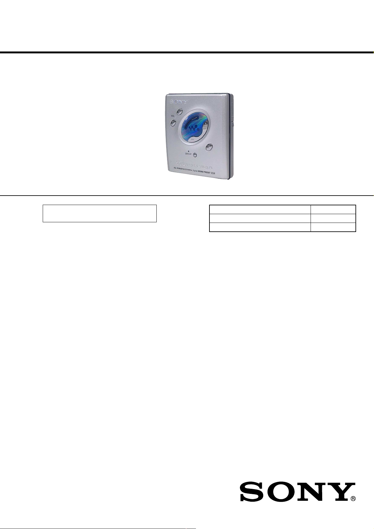
PORTABLE MINIDISC PLAYER
Page 2

MZ-E505
)
Battery life
Batteries
Ni-MH
rechargeable
battery
NH-14WM(A)
LR6 (SG)
Sony Alkaline
dry battery
LR6 (SG)4) and
NH-14WM(A)
1)
Measured with the power save function on (see
“Preserving battery power”) is on.
2)
Measured in accordance with the JEITA (Japan
Electronics and Information Technology
Industries Association) standard (using a Sony
MDW-series Mini-disc).
3)
With a fully charged battery
4)
When using a Sony LR6 (SG) “STAMINA” alkaline
dry battery (produced in Japan).
On the A C power adaptor (for the
supplied battery charging stand)
• For use in your house: Use the supplied AC
power adaptor. Do not use any other AC
power adaptor since it may cause the player to
malfunction.
Design and specifications are subject to change
without notice.
1)
(Unit: Approx. hours) (JEITA
SP
Stereo
(normal)
33 37 43
3)
49 54 64
4)
87 97 120
3)
Polarity of the plug
LP2 LP4
Stereo Stereo
2)
TABLE OF CONTENTS
1. SERVICING NOTES ............................................... 3
2. GENERAL ................................................................... 4
3. DISASSEMBLY
3-1. Disassembly Flow ........................................................... 5
3-2. Battery Case Lid.............................................................. 6
3-3. Case (Rear) ...................................................................... 6
3-4. MAIN Board ................................................................... 7
3-5. Upper Panel Section........................................................ 7
3-6. SWITCH Board............................................................... 8
3-7. Holder Assy (Z) ............................................................... 8
3-8. Mechanism Deck (MT-MZE505-176)............................ 9
3-9. Bracket (L) Assy ............................................................. 10
3-10. Br ac ket (R) Assy ............................................................. 10
3-11. Optical Pick-up (LCX-4E) .............................................. 11
3-12. DC SSM18B Motor (Spindle) (M901) ........................... 11
3-13. DC Motor (Sled) (M902) ................................................ 12
4. TEST MODE.............................................................. 13
5. ELECTRICAL ADJUSTMENTS......................... 18
6. DIAGRAMS
6-1. Block Diagram ................................................................ 24
6-2. Note for Printed Wiring Boards and
Schematic Diagrams ....................................................... 25
6-3. Printed Wiring Board
– MAIN Board (Component Side) – ............................. 26
6-4. Printed Wiring Board
– MAIN Board (Conductor Side) – ............................... 27
6-5. Schematic Diagram – MAIN Board (1/3) – .................. 28
6-6. Schematic Diagram – MAIN Board (2/3) – .................. 29
6-7. Schematic Diagram – MAIN Board (3/3) – .................. 30
6-8. IC Pin Function Description ........................................... 34
SAFETY-RELATED COMPONENT WARNING!!
COMPONENTS IDENTIFIED BY MARK 0 OR DOTTED
LINE WITH MARK 0 ON THE SCHEMATIC DIAGRAMS
AND IN THE PARTS LIST ARE CRITICAL TO SAFE
OPERATION. REPLACE THESE COMPONENTS WITH
SONY PARTS WHOSE PART NUMBERS APPEAR AS
SHOWN IN THIS MANU AL OR IN SUPPLEMENTS PUBLISHED BY SONY.
7. EXPLODED VIEWS
7-1. Upper Panel, Case (Rear) Section .................................. 40
7-2. Ornamental Belt Section ................................................. 41
7-3. Mechanism Deck Section (MT-MZE505-176) .............. 42
8. ELECTRICAL PARTS LIST ............................... 43
CAUTION
Use of controls or adjustments or performance of procedures
other than those specified herein may result in hazardous radiation exposure.
2
Page 3
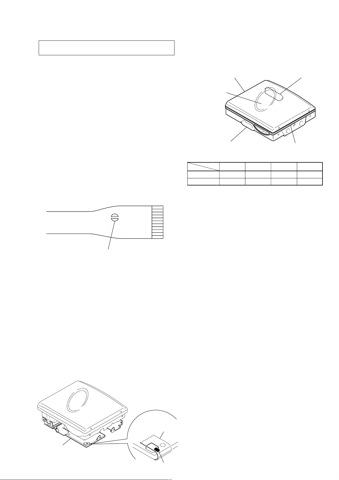
SECTION 1
upper panel (silver) battery case lid (silver)
case (rear) (silver)
ornamental belt (violet)
window (ornament)
(violet)
SERVICING NOTES
MZ-E505
NOTES ON HANDLING THE OPTICAL PICK-UP
BLOCK OR BASE UNIT
The laser diode in the optical pick-up block may suffer electrostatic break-down because of the potential difference generated
by the charged electrostatic load, etc. on clothing and the human
body.
During repair, pay attention to electrostatic break-down and also
use the procedure in the printed matter which is included in the
repair parts.
The flexible board is easily damaged and should be handled with
care.
NOTES ON LASER DIODE EMISSION CHECK
Never look into the laser diode emission from right above when
checking it for adjustment. It is feared that you will lose your sight.
NOTES ON HANDLING THE OPTICAL PICK-UP BLOCK
(LCX-4E)
The laser diode in the optical pick-up block may suffer electrostatic break-down easily. When handling it, perform soldering
bridge to the laser-tap on the flexible board. Also perform measures against electrostatic break-down sufficiently before the operation. The flexible board is easily damaged and should be handled
with care.
ABOUT VIOLET -COLOR-TYPE
Not a whole set of the violet-color-type is colored violet, but only
the ornamental belt and window (ornament) is violet, and the upper panel, the case (rear) and the battery case lid are colored silver.
COLOR V ARIA TION
SILVER BLUE PINK
E a –––
Hong Kong aaaa
• Replacement of CXD2671-210GA (IC601) used in this set requires a special tool.
VIOLET
laser-tap
OPTICAL PICK-UP FLEXIBLE BOARD
Notes on chip component replacement
• Never reuse a disconnected chip component.
• Notice that the minus side of a tantalum capacitor may be dam-
aged by heat.
Flexible Circuit Board Repairing
• Keep the temperature of the soldering iron around 270 ˚C during repairing.
• Do not touch the soldering iron on the same conductor of the
circuit board (within 3 times).
• Be careful not to apply force on the conductor when soldering
or unsoldering.
• In performing the repair with the power supplied to the set, removing the MAIN board causes the set to be disabled.
In such a case, fix a conve x part of the open/close detect switch
(S809 on MAIN board) with a tape in advance.
UNLEADED SOLDER
Boards requiring use of unleaded solder are printed with the leadfree mark (LF) indicating the solder contains no lead.
(Caution: Some printed circuit boards may not come printed with
the lead free mark due to their particular size)
main board
tape
S809
3
Page 4
MZ-E505
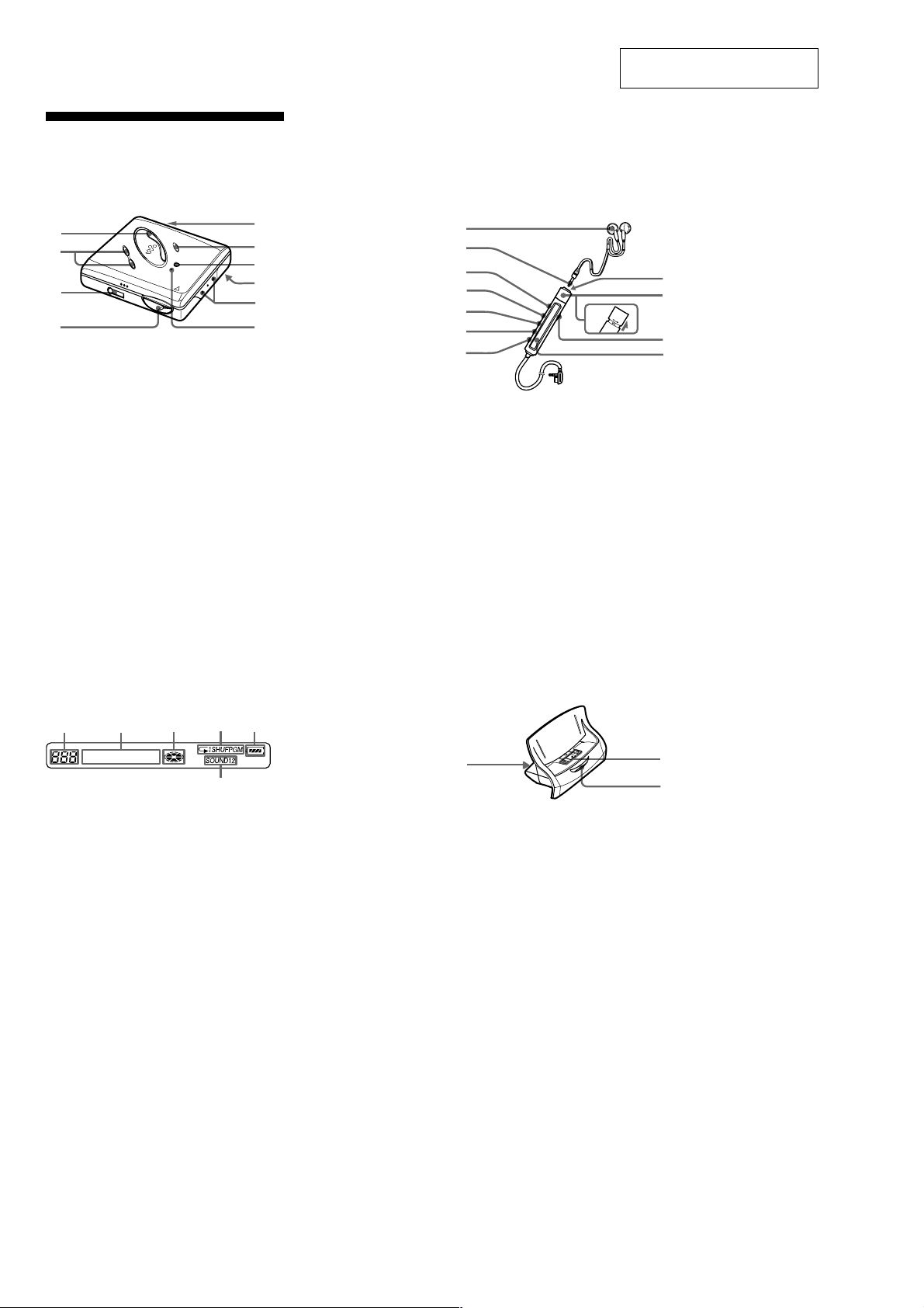
Parts and controls
SECTION 2
GENERAL
This section is extracted from
instruction manual.
The Player
1
2
3
4
1 ./
2 VOL +*/– button
3 i (earphones) jack
4 OPEN switch
5 Battery compartment
6 GROUP button
7 x button
8 HOLD (Locking the control) switch
9 Terminals for charging stand/
q; 3 Color Info-LED
* The
N>*
button
dry battery case (at the bottom)
N>
dots.
and VOL + buttons have tactile
5
6
7
8
9
q;
The earphones with a remote
control
1
2
3
4
5
6
q;
+
–
7
1 Headphones/earphones
2 Stereo mini plug
3 X (pause) button
4 SOUND button
5 RPT/ENT (Repeat/Enter) button
6 PLAYMODE button
7 DISPLAY button
8 x (stop) button**
9 Control ( ./
q; Control VOL +/–
Pull and turn to adjust the volume.
qa HOLD (Locking the control) switch
qs Display window
** The stop button also operates as the enter
button, depending on the function.
N>
)
8
9
qa
qs
The display window of the remote
control
1
2
3
4
6
1 Track number display
2 Charactor information display
3 Disc indication
4 Play mode indication
5 Battery level indication
6 SOUND indication
5
The battery charging stand
3
1 Terminals for charging
2 CHARGE lamp
3 DC IN 3V jack (at the rear)
1
2
4
Page 5
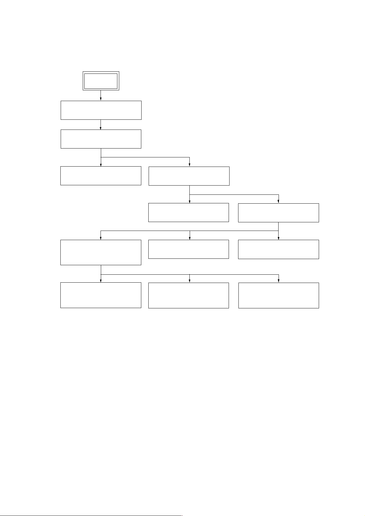
• This set can be disassembled in the order shown below.
3-1. DISASSEMBLY FLOW
SET
3-2. BATTERY CASE LID
(Page 6)
3-3. CASE (REAR)
(Page 6)
MZ-E505
SECTION 3
DISASSEMBLY
3-4. MAIN BOARD
(Page 7)
3-8. MECHANISM DECK
(MT-MZE505-176)
(Page 9)
3-11. OPTICAL PICK-UP
(LCX-4E)
(Page 11)
3-5. UPPER PANEL SECTION
(Page 7)
3-6. SWITCH BOARD
(Page 8)
3-9. BRACKET (L) ASSY
(Page 10)
3-12. DC SSM18B MOTOR
(SPINDLE) (M901)
(Page 11)
3-7. HOLDER ASSY (Z)
(Page 8)
3-10. BRACKET (R) ASSY
(Page 10)
3-13. DC MOTOR
(SLED) (M902)
(Page 12)
5
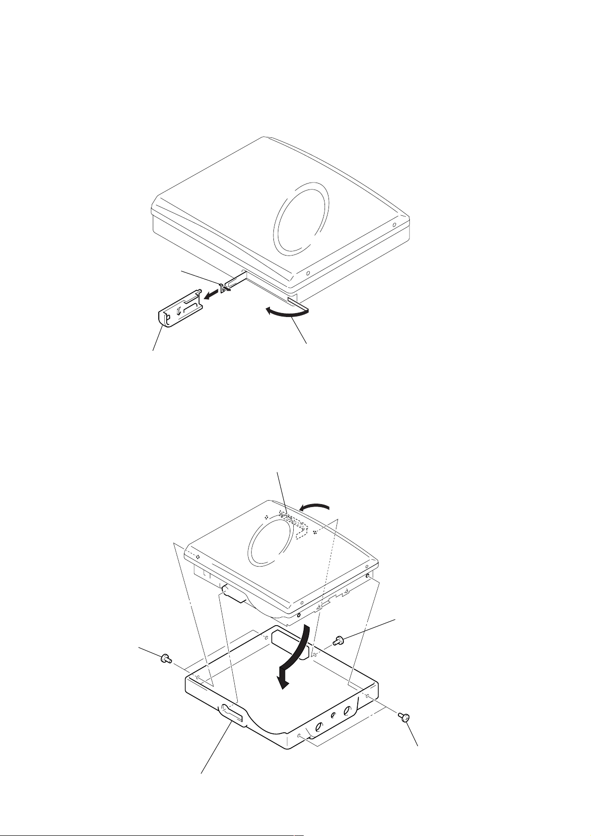
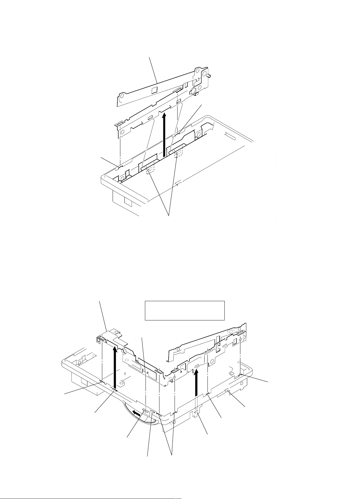
Page 6
MZ-E505
)
Note: Follow the disassembly procedure in the numerical order given.
3-2. BATTERY CASE LID
2
claw
3-3. CASE (REAR)
3
battery case lid
1
Open the battery case lid.
1
Close the battery terminal board assy.
2
screw (1.7)
3
two screws (M1.4)
3
two screws (M1.4
4
Remove the case (rear) in the
direction of the arrow.
6
Page 7
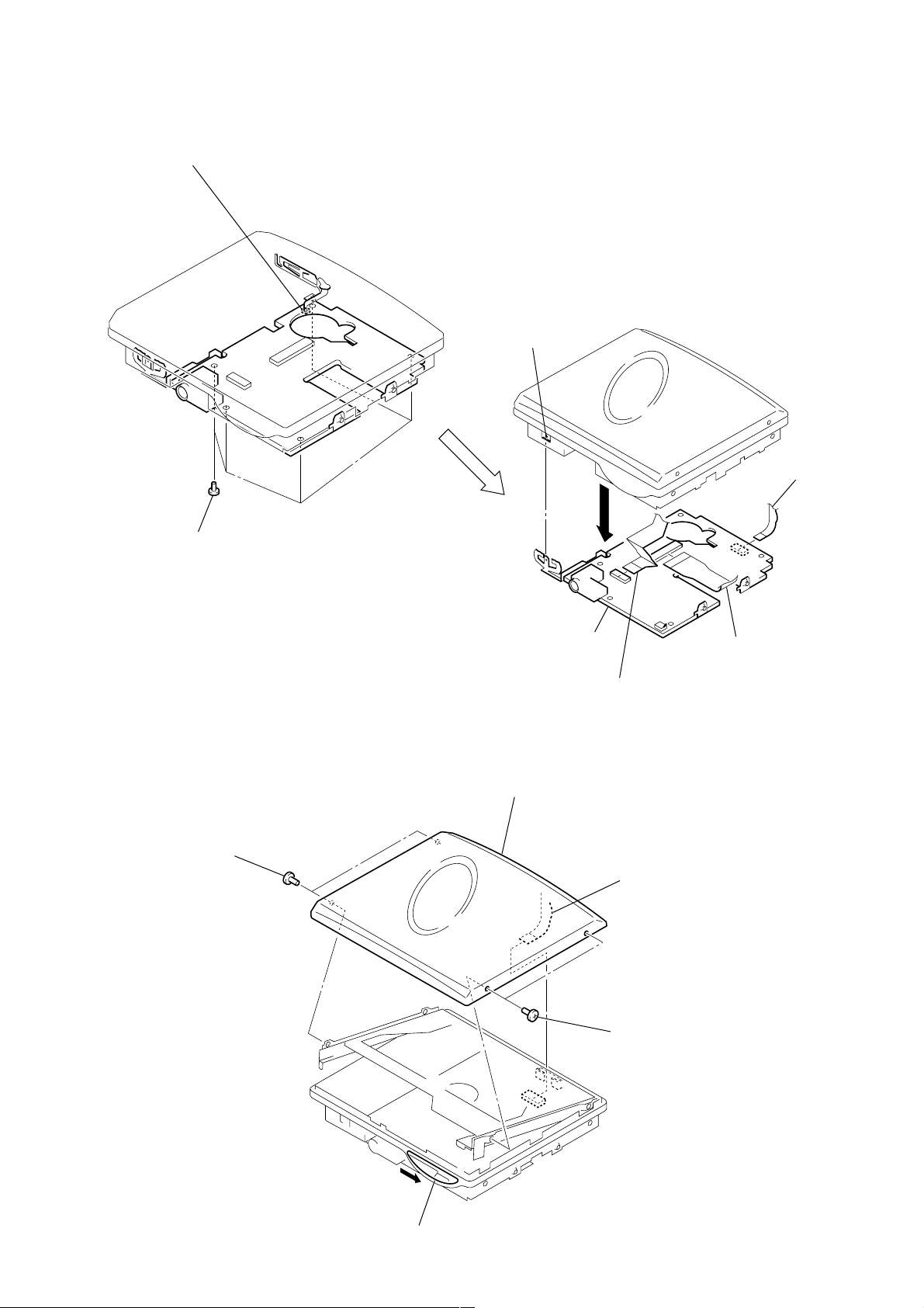
3-4. MAIN BOARD
8
main board
4
boss
5
7
flexible board (motor)
(CN551)
6
flexible board (optical pick-up)
(CN501)
3
flexible board
(switch board)
(CN801)
1
Remove solder of the
battery terminal board assy.
MZ-E505
2
five screws (M1.4 × 2)
3-5. UPPER PANEL SECTION
3
two screws (M1.4)
4
upper panel section
1
flexible board (switch board)
(CN801)
2
Open the upper section.
3
two screws (M1.4)
7
Page 8
MZ-E505
3-6. SWITCH BOARD
2
convex portion
2
3
switch board
convex portion
3-7. HOLDER ASSY (Z)
1
convex portion
2
1
four screws
(1.7 × 2.5)
4
holder assy (Z)
1
convex portion
3
two bosses
8
Page 9
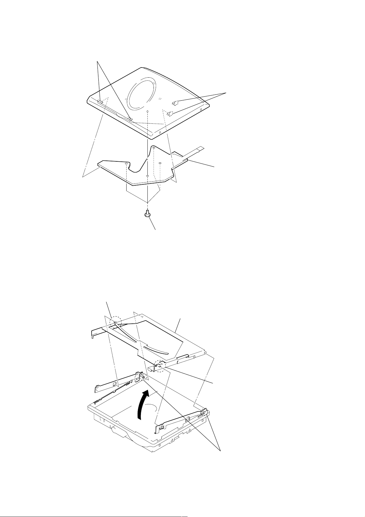
3-8. MECHANISM DECK (MT-MZE505-176)
1
step screw (L)
5
Lift up the mechanism deck
in the direction of the arrow.
MZ-E505
3
7
flexible board (motor)
(CN551)
claw
2
nut (M1.4)
8
mechanism deck (MT-MZE505-176)
4
convex portion
6
flexible board (optical pick-up)
(CN501)
9
Page 10
MZ-E505
3-9. BRACKET (L) ASSY
2
convex portion
3
bracket (L) assy
2
convex portion
3-10. BRACKET (R) ASSY
3
bracket (R) assy
1
two claws
Note: On installation, adjust the
position of knob (open) and
open slider.
open slider
2
convex portion
2
10
convex portion
1
claw
knob (open)
1
claw
2
convex portion
1
2
claw
1
claw
convex portion
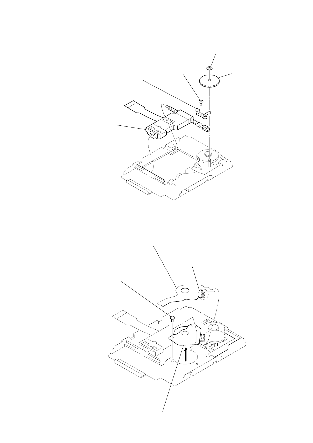
Page 11
)
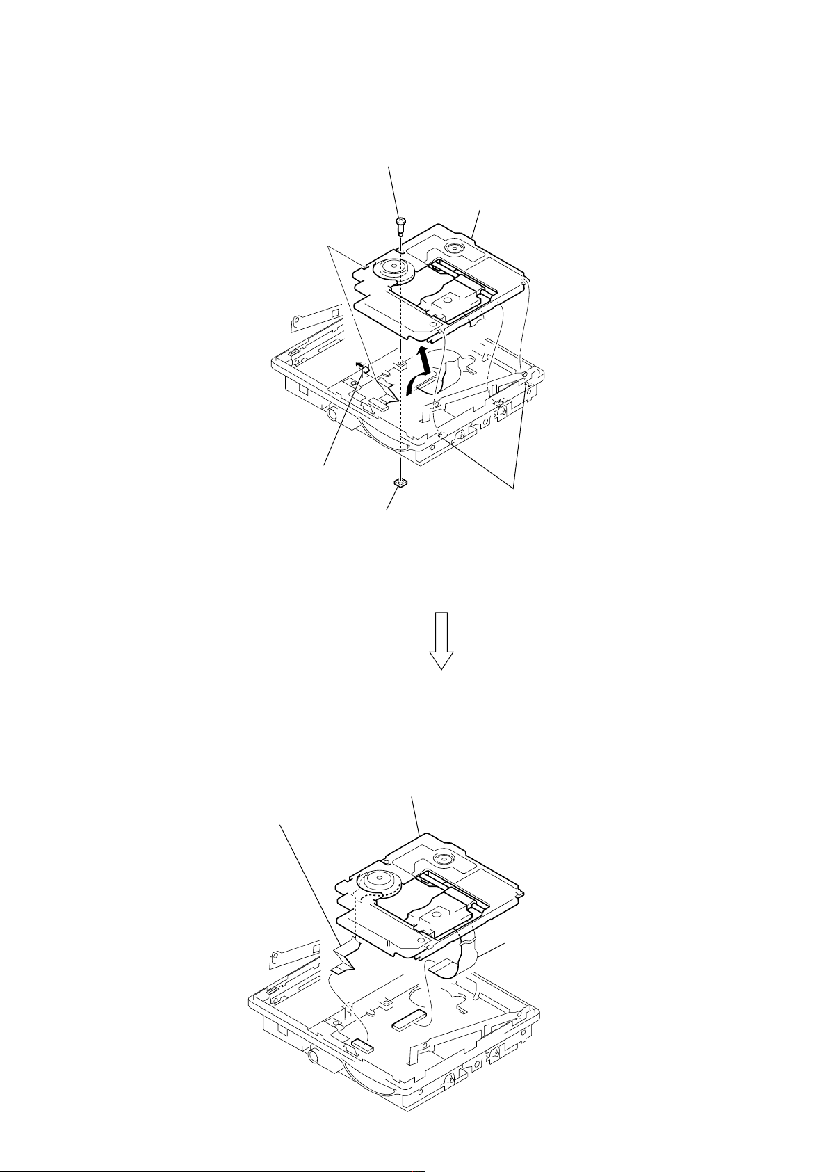
3-11. OPTICAL PICK-UP (LCX-4E)
4
thrust detent spring
5
optical pick-up (LCX-4E)
3
screw (M1.4)
1
washer
2
gear (SA
MZ-E505
3-12. DC SSM18B MOTOR (SPINDLE) (M901)
2
Remove the flexible board.
3
three tapping screws
1
Remove the four solders.
4
DC SSM18B motor (spindle) (M901)
11
Page 12
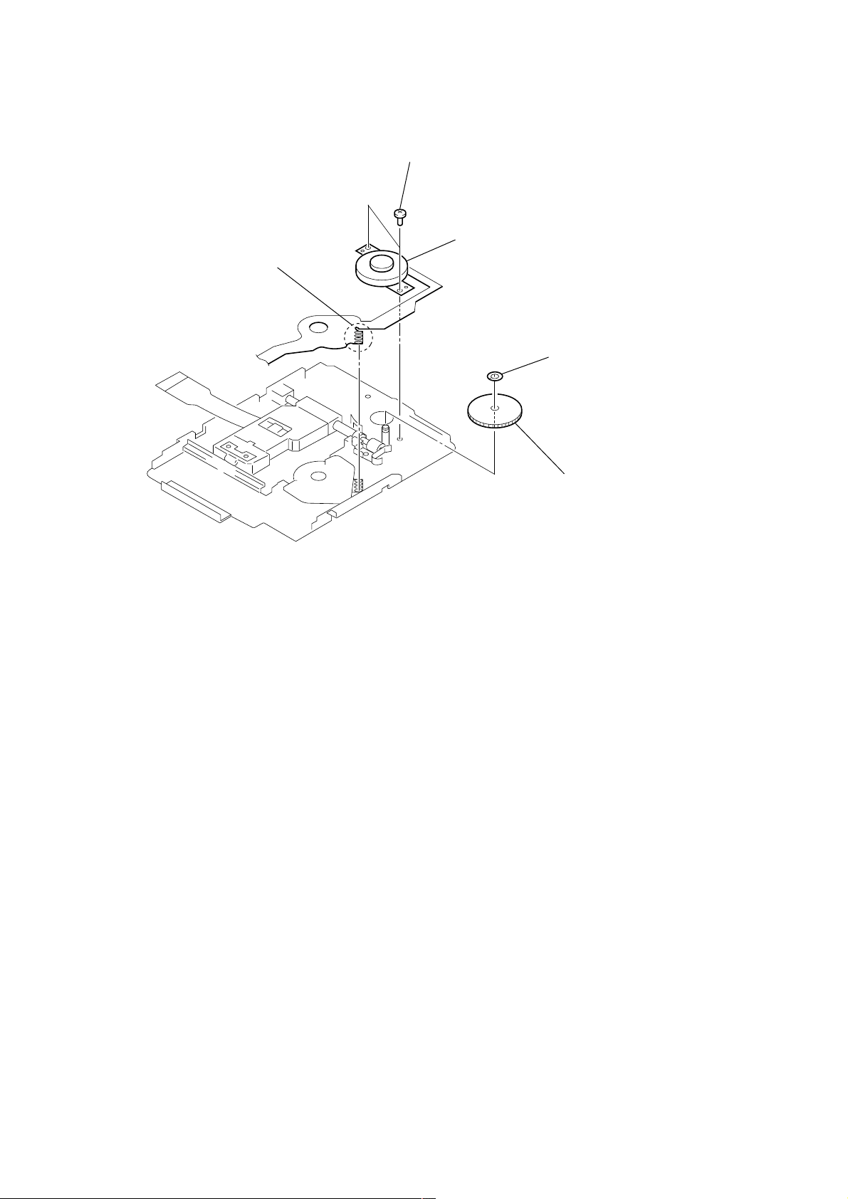
MZ-E505
)
3-13. DC MOTOR (SLED) (M902)
1
Remove the four solders.
4
two screws (M1.4)
5
DC motor (sled) (M902)
2
washer (0.8-2.5
3
gear (SA)
12
Page 13
SECTION 4
010 V2.200
All on
All off
Microprocessor
version
display
888
BASS12
TEST MODE
MZ-E505
4-1. GENERAL
• When entered in the TEST MODE, this set provides the Overall
Adjustment mode which allows CD and MO discs to be automatically adjusted. In the Overall Adjustment mode, the system
discriminates between CD and MO discs, performs adjustments
in sequence automatically, and displays the faulty location if
any fault is found. In the Manual mode, selected adjustments
can be performed automatically.
• The attached remote control is used to operate the TEST MODE.
Unless otherwise specified in the text, the key means that on the
remote control.
4-2. SETTING THE TEST MODE
4-2-1. How to set the TEST MODE
To set the TEST MODE, two methods are available.
1 Solder bridge and short TAP601 (TEST) on the main board.
Then turn on the power.
– MAIN BOARD (Component Side) –
Remote control LCD
• Press and hold down X key to hold the current display while
the key is being pressed.
4-2-3. How to release the TEST MODE
When method 1 was used:
Turn off the power and open the solder bridge on TAP601 on the
main board.
Note: The solder should be removed clean. The remaining solder
may make a short with the chassis and other part.
When method 2 was used:
Turn off the power.
2 In the normal mode, operate the keys on the set and those on the
4-2-2. Operations when the TEST MODE is set
When the TEST MODE is entered, the system switches to the display check mode within the TEST MODE. From this mode, the
other Test modes can be accessed.
When the TEST MODE is set, the LCD repeats a cycle of the following displays:
212194221196215184216176228173199
222219214198192186223217188220226162177
213200202225208210211209201203204155
C620
C615
R613
TAP601
(TEST)
remote control as specified below:
Turn on HOLD switch on the set. Holding down x (STOP)
key on the set, enter the keys on the remote control in the
following sequence:
> N t > N t . t . t > N
t . t > N t . t X t X
Note: When the power supply is switched on in the state where all
electrical adjustments have not finished, it is displayed on
LCD as “NV Error’’ and the usual operation can’t be per-
formed.
When a power supply is accidentally turn off in the middle
of electrical adjustments, it is again set as test mode and elec-
trical adjustments is mode to complete.
13
Page 14
MZ-E505
011 XXXS5E
address
mode number
adjusted value
011 OFEJ5E
jitter value
mode number
adjusted value
011 063B5E
block error value
mode number
adjusted value
011 072A5E
ADIP error value
mode number
adjusted value
011 LrefPw 5 E
item title
mode number
adjusted value
4-3. TEST MODE STRUCTURE
Test Mode
(Display Check Mode)
+
VOL
Manual Mode
x
key
+
VOL
VOL
.
Overall Adjustment Mode
x
key
DISPLAY key
x
key
>B
x
key
DISPLAY key
(Press and hold down about 3 sec)
Terminate key checking or open
the top panel.
Self-diagnostic Display Mode
Sound Skip Check Result Display Mode
Servo Mode
Audio Mode
Power Mode
OP Alignment Mode
Key Check Mode
3. Each test item is assigned with a three-digit item number. The
100th place is a major item, 10th place is a middle item, and unit
place is a minor item.
+
: 100th place of mode number
Change Major
Item
> N
Change Middle
Item
> N
Change Minor
Item
VOL
VOL
x
key
VOL
VOL
x
key
> N
.
Change Adjustment
Value
Write Adjustment
Value
X
key : When adjusted value is changed :
Adjusted value is written.
When adjusted value is not changed :
That item is adjusted automatically.
increase
: 100th place of mode number
decrease
+
: 10th place of mode number
increase
: 10th place of mode number
decrease
: Unit place of mode number
increase
: Unit place of mode number
decrease
VOL
VOL
+
: Up
: Down
4. During each test mode, the display is changed from one to
another each time DISPLAY key is pressed.
• Address & Adjusted Value Display
LCD display
4-4. MANUAL MODE
4-4-1. Outline of the function
The Manual mode is designed to perform adjustments and
operational checks on the set’s operation according to each
individual function.
Usually, no adjustments are made in this mode.
However, the Manual mode is used to clear the memory before
performing automatic adjustments in the Overall Adjustment mode.
4-4-2. How to set the Manual mode
1. Set the TEST MODE and turn the control towerd V OL + to set
the Manual mode.
Remote control LCD display
2. During each test, turn and hold the control towerd > N or
. for a while to mo ve the optical pickup on the sled outer or
000 Manual
inner perimeter.
• Jitter Value & Adjusted Value Display
LCD display
• Block Error Value & Adjusted Value Displa y
LCD display
• ADIP Error Value & Adjusted Value Display
LCD display
• Item Title Display
LCD display
14
Note: In the Power mode, the item title display is only displayed.
Page 15

5. To terminate the Manual mode and return to the TEST MODE,
press x key.
4-5. OVERALL ADJUSTMENT MODE
4-5-1. Outline of the function
This mode is designed to adjust the servo system automatically by
going through all the adjustment items.
Usually, this mode is used to perform automatic adjustments when
servicing the set.
For further information, refer to section 5. ELECTRICAL ADJUSTMENTS. (See page 18)
4-6. SELF-DIAGNOSTIC DISPLAY MODE
4-6-1. Outline of the function
The Self-diagnostic system is used in this set. If an error occurs
during playback, this system detects the fault through the
microprocessor’s mechanism and power control blocks and stores
the cause in EEPROM in a history format.
This history, which can be viewed in the TEST MODE, provides
the means of locating the fault in troubleshooting.
MZ-E505
4-6-2. Self-diagnostic mode
1. Set the TEST MODE.
2. With all the LCD display segments blinking on the set, press
DISPLAY key and turn the control towards >B , the Selfdiagnostic mode is entered.
001 1 Adrs
History code
Error display code
3. Hereinafter, each time > N is turned the control towards,
the reference information display changes as follows:
0XX1 # # # #
0XXN # # # #
0XXN1# # # #
0XXN2# # # #
0XXR
Simplified contents
– – – –
_
• Turn the control towards . to go back to the previous
display.
• Contents of the history codes
History code number
1 The first error that occurred.
N The last error that occurred.
N1 The first error from the last one.
N2 The second error from the last one.
R_
T otal recording time ( – – – – is displayed
for this set)
Contents
15
Page 16

MZ-E505
• Description of the error display codes
Contents of fault Display code Meaning of code
No error 00 No error – – – – No error
01 Access target address illegally specified Adrs An attempt to access an abnormal address.
Servo system error
TOC error
Power system error 22 LOWBATT LBat Instantaneous interruption detected.
Offset error
4-6-3. Clearing the error display code
After servicing, reset the error display code.
1. Set the TEST MODE.
2. Press the DISPLAY key on the remote control acti v ates the self-
diagnosis display mode.
3. To reset the error display code press X key on the remote con-
trol when the code is displayed.(except for R_ - - - - display)
(All the data on the 1, N, N1 and N2 will be reset)
4. Press X key on the remote control again.
02 HIGH TEMP Temp HIGH TEMP
03 FOCUS ERROR Fcus Focus off-center.
04 SPINDLE ERROR Spdl Abnormal rotation of disc
11 TOC ERROR TOC
12 READ DATA ERROR Data
31 OFFSET ERROR Ofst Offset error
32 FE_ABCD_OFFSET_ERR ABCD FE ABCD Offset error
33 TE_ABCD_OFFSET_ERR TE TE ABCD Offset error
34 X1_TE_OFFSET_ERR X1TE X1 TE ABCD Offset error
Simplified
contents
Description
16
Page 17

MZ-E505
4-7. SOUND SKIP CHECK RESULT DISPLAY MODE
This set can display and check the error count occurring during
play.
• Setting method of Sound Skip Check Result Display Mode
1. Setting the test mode.
2. Turn the control towards > N activates the sound skip
check result display mode where the LCD displays as shown
below.
LCD display
000 P**P##
Total of play system
error count
Total of record system error count
3. When > N is tur ned the control to wards, the total of error
count is displayed on the LCD, and each time the > N is
turned the control towards, the error count descents one by one
as shown below. Also, when . is turned the control to-
wards, the error count ascends by one.
000 P**R00
000 EIB **
4-8. KEY CHECK MODE
4-8-1. Outline of the function
This mode is used to check to make sure that each of the keys
(including the slide switch) on the set operates normally.
4-8-2. Setting the Key Check mode
1. Set the TEST MODE. Press and hold down DISPLAY key (for
more than 3 sec) to set the Key Check mode.
LCD display
000 0F
2. When each key on the set and on remote control is pressed, its
name is displayed on the LCD. (The operated position is displayed for 4 sec after the slide switch is operated. If any other
key is pressed during this display , the LCD switches to its name
display)
Example: When > N key on the set is pressed:
LCD display
000 FF 0F
Example: When > N on the remote control is turned the
control towards:
LCD display
000 Stat**
000 Adrs**
000 BEmp**
000 ######
P**R00 : Total of play system error and record system error count
** : Sound skip check items counter (hexadecimal)
##### : 6-digit address (hexadecimal) where a sound skipped
Error code
Cause of error Description of error
Playback EIB Sound error correction error
Stat Decorder status error
Adrs Cannot access the address
BEmp Buffer becomes empty
4. Quit the sound skip check result display mode, and press the x
key to return to the test mode. (display check mode)
000 rPLAY XX
XX: AD v alue of the remote control key (hexadecimal 00 to FF)
3. When all the keys on the set and on the remote control are considered as OK, the following displays are shown for 2 sec.
(The key pressed to enter the Ke y Check mode has been checked
even if it is not pressed in this mode)
Example: When the keys on the set are considered as OK:
LCD display
888 SET OK OF
Example: When the keys on the remote control are considered
as OK:
LCD display
888 RMC OK OX
4. When all the key have been checked or when the top panel is
opened during this checking, the system terminates the Key
Check mode and return to the TEST MODE.
17
Page 18

MZ-E505
r
SECTION 5
ELECTRICAL ADJUSTMENTS
5-1. GENERAL
In this set, CD and MO discs can be automatically adjusted by setting the Overall Adjustment mode within the TEST MODE,
Before performing these automatic adjustments, it is necessary to
clear the memory and adjust the power in the Manual mode.
5-2. NOTES FOR ADJUSTMENT
5-2-1. Jigs
• CD disc TDYS-1 (part code: 4-963-646-01)
• MO disc PTDM-1 (part code: J-2501-054-A)
or commercially available MO disc (recorded)
• Digital voltmeter
• Ammeter
5-2-2. Adjustment sequence
The adjustments should be always performed in the following
sequence:
1 Reset NV (Clear the memory)
Manual mode
2 Manual power adjustments
3 Electrical offset adjustments
(Do not enter the disc)
4 Overall CD adjustments
5 Overall MO adjustments
Overall adjustment mode
5-4. MANUAL POWER ADJUSTMENTS
5-4-1. Adjustment sequence
The adjustments should be always performed in the following sequence:
1 Vc PWM Duty (L) adjustment (item No.:762)
r
2 Vl PWM Duty adjustment (item No.:764)
r
3 Vb A/D value check (item No.:731)
5-4-2. Vc PWM Duty (L) adjustment
Connection:
digital
voltmete
MAIN board
TP901 (VC)
TP921 (GND)
Procedure:
1. Confirm that the power voltage is at 1.5 V DC.
2. Set the TEST MODE.
3. Set the overall adjustment mode and press PLAYMODE key,
item No. will change to 762.
LCD display
6 RESUME clear
7 Rewrite the NV value
5-2-3. Power
The power is supplied with 1.5 V DC from the battery case.
5-3. RESET NV
5-3-1. How to reset NV
1. Set the TEST MODE.
2. Set the Manual mode and set the item No. 021, Reset NV.
LCD display
021 Res NV CC
3. Press X key on the remote control.
LCD display
021 Res OK?
4. Press X key on the remote control again.
LCD display
762 VclPWM XX
4. Connect a digital voltmeter to TP901 (VC) and TP921 (GND)
on the main board and adjust V OL + (v oltage up) and V OL –
(voltage down) on the remote control.
Adjustment value:2.35V
Standard value:2.34 to 2.355V
5. Press X key to write the adjustment value.
021 Res ***
After reset is completed.
021 Reset!
5. Press x key to terminate the Manual mode and return to the
TEST MODE.
18
Page 19

MZ-E505
TEST MODE
(Display Check Mode)
Overall Adjustment
Title Display(ASSY**)
CD overall
Adjustment
.
key
x
MO overall
Adjustment
> N
> N
key
x
Electrical offset
Adjustment key
DISPLAY key
key
x
key
x
Power Supply
Adjustment
PLAY MODE key
VOL
r
5-4-3. VI PWM Duty adjustment
Connection:
digital
voltmete
MAIN board
TP904 (VL)
TP921 (GND)
Procedure:
1. Set the Manual mode and set the item No. to 764.
LCD display
764 VlPWM XX
2. Connect a digital voltmeter to TP904 (VL) and TP921 (GND)
on the main board and adjust VOL + (Voltage up) and VOL –
(Voltage down) on the remote control.
Adjustment value:2.23V
Standard value:2.22 to 2.235V
3. Press X key to write the adjustment value.
5-4-4. Vb A/D value check
1. Set the Manual mode and set the item No. to 731.
LCD display
731 Vb_AD XX
2. Confirm the A/D value is 73 to 87 hex.
3. Confirm the power supply consumiption current is 120 mA or
less.
5-5. OVERALL ADJUSTMENT MODE
5-5-1. Overall adjustment mode structure
Note: The overall adjustments should be always performed in the
sequence of CD t MO adjustments.
5-5-2. Overall CD and MO adjustment method
1. Set the TEST MODE and turn the control towards VOL – to
set the Overall Adjustment mode.
LCD display
000 Assy11
5-4-5.Electrical offset adjustment method
Note: Doing adjustment by the state that a disc does not enter.
1. Confirm the power voltage is 1.5V.
2. Set to the test mode.
3. Turn the control towards VOL – activates the overall adjust-
ment mode.
LCD display
4. Press the DISPLAY key.
LCD display
5. If result of electrical offset adjustment is OK,the following display appears.
LCD display
000 Assy11
035 Ofst**
000 OfstOK
2. Insert CD disc in the set, and turn the control towards . to
set the Overall CD Adjustment mode.
Automatic adjustments are made.
LCD display
XXX CD RUN
XXX: Item No. for which an adjustment is being executed.
3. If NG in the overall CD adjustments, return to Reset NV and
perform from the electrical offset adjustment again.
LCD display
000 XXX NG
XXX: NG item No.
4. If OK through the overall CD adjustments, then perform overall
MO adjustments.
LCD display
000 CD OK
5. Insert MO disc in the set, and turn the control towards > N
to set the Overall MO Adjustment mode. Automatic adjustments
are made.
LCD display
XXX MO RUN
XXX: Item No. for which an adjustment is being executed.
19
Page 20

MZ-E505
6. If NG in the overall MO adjustments, return to Reset NV and
perform the adjustment again.
LCD display
000 XXX NG
XXX: NG item No.
7. If OK through the overall MO adjustments, press x key to
return to the TEST MODE and terminate the Overall Adjustment mode.
LCD display
000 MO OK
5-5-3.Resume clear method
1. Setting the testmode.
2. Set the Manual mode and set the item No.041 (NoClock).
LCD display
041 NoClock
3. Press the X key.
LCD display
041 Res ***
After reset is completed
LCD display
041 ResClr
5-5-4. Rewrite the NV value
After resume clear, rewrite the NV value.
Item NO. NV value
861 0F (h)
862 0B (h)
863 C7 (h)
864 01 (h)
865 64 (h)
866 10 (h)
867 65 (h)
868 05 (h)
5-5-5. Overall CD and MO adjustment items
1. Overall offset adjustment
Item No. Contents
030 GRV setting • Sarvo OFF • Head UP
035 Laser ON/OFF electrical offset difference
measurement
Completed
2. Overall CD adjustment items
Item No. Contents
761 VC,VR power voltage High/Low selection
300 HPIT setting • Sarvo OFF
561 SLED move to inside
562 SLED move to outside
High reflection CD electrical offset adjustment
312
313 IJ offset adjustment
314 FE offset adjustment
320 Focus servo ON
324 TE offset adjustment 1
321 TE gain adjustment
328 TWPP gain adjustment
324 TE offset adjustment 1
332 TE offset adjustment 2
330 Tracking servo ON
336 ABCD gain adjustment
337 KF gain correction
338 RF gain adjustment
344 CD focus gain adjustment
345 CD tracking gain adjustment
521 CD two-axis sensitivity adjustment (inside)
522 CD two-axis sensitivity adjustment (outside)
300 HPIT setting • servo OFF
completed
Laser ON • Focus UP • VC correction ALFA offset
adjustment
HPIT adjustment
3. Overall MO adjustment items
Item No. Contents
761 VC,VR power voltage High/Low selection
100 G RV setting
Low reflect MO offset adjustment
112 Laser ON • Focus UP • EVC correction ALFA offset
adjustment
113 IJ offset adjustment
114 FE offset adjustment
118 Wpp denominator adjustment
HPIT adjustmet
200 LPIT setting • servo OFF
561 SLED move to inside
220 Focus servo ON
224 TE offset adjustment 1
221 TE gain adjustment
224 TE offset adjustment 1
232 TE offset adjustment 2
20
Page 21

MZ-E505
digital
voltmeter
MAIN board
TP902 (VCOUT)
TP815 (LEDADJ)
Item No. Contents
230 Tracking servo ON
236 ABCD gain adjustment
237 KF gain adjustment
238 RF gain adjustment
244 FCS gain adjustment
245 TRK gain adjustment
READ GRV adjustment 1
100 R GRV setting
562 SLED move to outside
120 Focus servo OFF
122 TON offset adjustment
121 TE gain adjustment
122 TON offset adjustment
123 TEIN offset adjustment
124 TWPP offset adjustment
130 Tracking servo ON
131 TWPP offset adjustment
136 ABCD gain adjustment
137 KF gain adjustment
139 ADIP BPF fo adjustment
144 FCS gain adjustment
145 TRK gain adjustment
134 TWPP gain adjustment
131 TWPP offset adjustment 1
132 TWPP offset adjustment 2
149 TWPP OP offset adjustment
138 RF gain adjustment
100 R GRV setting • Servo OFF
5-6. LED VOLTAGE ADJUSTMENTS
5-6-1. LED voltage check
Connection:
Procedure:
1. Confirm the power voltage is at 1.5 V.
2. Set to the test mode.
3. Set the Manual mode and set the item No. to 071.
Connect a digital voltmeter to TP902 (VCOUT) and TP815
(LEDADJ) on the MAIN board and confirm the voltage (high
luminosity RED voltage value).
LCD display
071 Red35H XX
XXX: A/D value.
4. Turn the control towards VOL + four times to change the item
No. to 075.
Connect a digital voltmeter to TP902 (VCOUT) and TP815
(LEDADJ) on the MAIN board and confirm the voltage (high
luminosity GREEN voltage value).
LCD display
075 GRN35H XX
XXX: A/D value.
21
Page 22

MZ-E505
5. Judge LED voltage value is OK or NG by using the voltage v alue
confirmed at step 3 and 4.
IN case of jadgment result is NG, adjust the LED voltage (See
page 23).
flow chart of judging LED voltage is OK or NG:
Vred: High luminosity RED voltage value (item No. 071)
Strat
Vgrn: High luminosity GREEN voltage value (item No. 075)
0.500mV Vred 1.100mV?
OK
2.300mV Vgrn 4.500mV?
OK
Set the item No. to 081
and confirm the LED
color is orange.
End
NG
Vred 1.101mV
Vred-Vgrn (adsolute value)
2.000mV?
OK OK
NG
Vgrn-Vred (absolute value)
3.500mV?
OK OK
Vred
0.419mV
NG NG
8-2. LED voltage adjustment
(See page 23)
NG NG
8-2. LED voltage adjustment
(See page 23)
Vred-Vgrn (adsolute value)
Vgrn-Vred (absolute value)
0.420mV Vred 0.499mV
2.000mV?
1.350mV Vgrn 2.299mVVgrn 1.349mVVgrn 4.501mV
0.800mV?
22
Page 23

MZ-E505
r
5-6-2. LED voltage adjustment
Note: This adjustment performed only when the judgment result
of judging LED voltage value is OK or NG is NG
(See page 22).
Connection:
digital
voltmete
MAIN board
TP902 (VCOUT)
TP815 (LEDADJ)
Procedure:
1. Set the Manual mode and set the item No. to 071.
LCD display
071 Red35H XX
XXX: A/D value.
2. Connect a digital voltmeter to TP902 (VCOUT) and TP815
(LEDADJ) on the MAIN board and adjust with V OL + (Voltage up) and VOL – (Voltage down) so that the voltage becomes standard value.
Standard value: 0.500 to 1.100 mV
3. Press X key to write the adjustment value.
4. Set the Manual mode and set the item No. to 075.
LCD display
Connecting Location:
– MAIN BOARD (Component Side) –
TP815
(LEDADJ)
TP902
(VCOUT)
IC601
CN801
IC901
TP904
(VL)
TP921
(GND)
IC301
TP901
(VC)
075 GRN35H XX
XXX: A/D value.
5. Connect a digital voltmeter to TP902 (VCOUT) and TP815
(LEDADJ) on the MAIN board and adjust with V OL + (Voltage up) and VOL – (Voltage down) so that the voltage becomes standard value.
Standard value: 2.300 to 4.500 mV
6. Press X key to write the adjustment value.
2323
Page 24

MZ-E505
6-1. BLOCK DIAGRAM
SECTION 6
DIAGRAMS
JX JY JX
IX IY IX
ABCD
OPTICAL PICK-UP BLOCK
(FOCUS)
M902
(SLED)
M901
(SPINDLE)
Iy
Ix
Jx
Jy
A
B
C
D
PD
LD
(LCX-4E)
2-AXIS
DEVICE
(TRACKING)
U
WV
U
WV
RF AMP,FOCUS/TRACKING ERROR AMP
VREF
4
Iy
8
Ix
9
Jx
10
Jy
11
A
12
B
14
C
5
D
6
A-C
13
D-C
7
PD-NI
18
LD-A
S0
S0
S1
S1
TRK+
TRK-
FCS+
FCS-
LASER
AUTO POWER
CONTROL
Q501
PD-O
20
CPVI2
24
COM2
26
CPWI2
23
CPUI2
25
FO2
30
RO2
32
FO1
13
RO1
11
WO2
39
UO2
35
VO2
37
CPWI1
20
CPVI1
19
COM1
17
CPUI1
18
UO1
8
VO1
6
WO1
4
IC501
RF AMP,
FOCUS
ERROR,
TRACKING
ERROR
TPP/WPP
APC
PRE
DRIVER
PRE
DRIVER
PRE
DRIVER
PRE
DRIVER
PEAK
/BOTM
SERIAL
I/F
S-MONITOR
FOCUS/TRACKING COIL DRIVE,
SPINDLES/SLED MOTOR DRIVE
IC551
HI-BRIDGE
CONTROL/
PRE DRIVER
HI-BRIDGE
CONTROL/
PRE DRIVER
CONTROL/
PRE DRIVER
RF OUT
PEAK
BOTM
ABCD
ADIP IN
ADIP
PD-I
XRST
SBUS
SCK
S MON
CONTROL
3 PHASE
3 PHASE
HEADPHONE AMP
IC301
IN L
29
RFI
XCS
37
44
PEAK
BOTM
45
ABCD
46
47
FE
TE
56
ADFG
74
APCREF
78
49
VC
12
VREF MON
221
XRF RST
SSB DATA
160
161
SSB CLK
9
S MON
194
PD S0
195
PD S1
219
XCS NV
181
SCK0
S00
180
SI0
179
SLCV
101
SLCW
102
SLCU
100
TFDR
81
TRDR
80
FFDR
82
FRDR
83
SDW
99
98
SDV
SDU
96
SLD MON
233
SLVS
97
SPCW
95
94
SPCV
93
SPCU
SPDL MON
223
89
SPDV
90
SPDW
87
SPDU
88
SPVS
220
XRST MTR DRV
SYSTEM CONTROLLER,
DIGITAL SIGNAL PROCESSOR,
16M BIT D-RAM
IC601
33
29
28
41
FE
42
TE
1
44
21
19
31
VC
25
23
24
43
EEPROM
IC801
CPVO2
CPWO2
CPUO2
BIAS
OE
PWM2
CPWO1
CPVO1
CPUO1
PWM1
RI2
RI1
WI2
VI2
UI2
VI1
WI1
UI1
4DI3DO2CK1
46
47
45
FI2
28
27
FI1
15
16
41
42
43
44
52
53
54
1
2
56
55
OE
48
AOUTL
AOUTR
BEEP
XHP STBY
MUTE
RMC DTCK
LED RED PWM
LED GREEN PWM
SET KEY 1
WK DET
XHOLD SW
HALF LOCK SW
OSCI
OSCO
RMC KEY
VB MON
VC PWM
VL PWM
FS4
VLON
SLEEP
FFCLR
XRST
AVDD
30
183
240
218
142
167
163
13
17
227
19
24
25
20
10
165
164
86
234
235
236
8
21
UNREG
X601
45.1584MHz
22 2
IN R
21
BEEP
15
18
STB
MUTE
17
POWER CONTROL
IC901
DVDD
44
VD
5
XWK4
2
XWK1
7
VRMC
3
XWK2
26
INM1
RF1
27
23
RF2
22
INM2
56
CLK
1
VLON
55
SLEEP
54
FFCLR
46
XRST
36
VC
34
VC
45
VC2
OUT A BEEP
OUT B BEEP
BEEP
SWITCH
BOARD
S808
HOLD
OFF
ON
OPEN/CLOSE
DETECT
VLD
VIF
VCO
VG
LG
VL
VL
L2
L2
VB
XWK3
VSTB
L1
L1
VC OUT
S809
10
42
35
19
18
11
16
12
50
32
28
33
OUT L
OUT R
VREF IN
9
4
6
4
24
23
13
VL
VIF
VC
VG
D903
SWITCHING
Q910, 911
REFERENCE
VOLTAGE
SWITCHING
Q301
SIGNAL PATH
: PLAYBACK
D902
B+ SWITCH
Q908, 909
D901
L905
L902
L901
VOLTAGE
DETECTOR
IC903
RCH
LCH
J301
VC
RVDD
KEY
DATA
RGND
UNREG
RECHAGEABLE
BATTERY
NH-14WM
1PC, 1.2V 1350mAh
(BATTERY CASE)
DRY BATTERY
SIZE "AA"
(IEC DESIGNATION LR6)
1PC, 1.5V
2424
Page 25

6-2. NOTE FOR PRINTED WIRING BOARDS AND SCHEMATIC DIAGRAMS
e
p
p
p
p
p
p
Note on Printed Wiring Board:
• X : parts extracted from the component side.
• Y : parts extracted from the conductor side.
• : Pattern from the side which enables seeing.
(The other layers' patterns are not indicated.)
Caution:
Pattern face side: Parts on the pattern face side seen from
(Conductor Side) the pattern face are indicated.
Parts face side: Parts on the par ts face side seen from
(Component Side) the parts face are indicated.
• MAIN board is four-layer printed board.
However, the patterns of layers 2 and 3 have not been
included in this diagrams.
* Replacement of IC601 used in this set requires a spe-
cial tool.
• Lead Layouts
Lead layout of conv entional IC CSP (chip size package)
surfac
Note on Schematic Diagram:
• All capacitors are in µF unless otherwise noted. pF: µµF
50 WV or less are not indicated except for electrolytics
and tantalums.
• All resistors are in Ω and 1/
specified.
• C : panel designation.
• A : B+ Line.
Note: The components identified by mark 0 or dotted line
with mark 0 are critical for safety.
Replace only with part number specified.
• Total current is measured with MD installed.
• Po wer voltage is dc 3 V and f ed with regulated dc power
supply from external power voltage jack.
• V oltages and wa v eforms are dc with respect to ground in
playback mode (servo circuit ON).
no mark : PLAYBACK
• V oltages are taken with a VOM (Input impedance 10 MΩ).
Voltage variations may be noted due to normal production tolerances.
• Waveforms are taken with a oscilloscope.
Voltage variations may be noted due to normal production tolerances.
• Circled numbers refer to waveforms.
• Signal path.
E : PLAYBACK
: Impossible to measure
∗
4
W or less unless otherwise
• Waveforms
1 IC501 1 (TE)
200 mV/DIV, 1 µs/DIV
2 IC501 8 (Iy)
100 mV/DIV, 1 µs/DIV
Approx.
760 mVp-p
200 mVp-
6 IC501 ed (RF OUT)
500 mV/DIV, 500 ns/DIV
7 IC501 rs (FE)
200 mV/DIV, 1 µs/DIV
1.0 Vp-p
Approx.
620 mVp-
MZ-E505
qa IC601 th (TE)
200 mV/DIV, 1 µs/DIV
Approx.
760 mVp-p
qs IC601 ih (FS4)
500 mV/DIV, 2 µs/DIV
1.9 Vp-p
5.68 µs
* Replacement of IC601 used in this set requires a spe-
cial tool.
• The voltage and waveform of CSP (chip size package)
cannot be measured, because its lead layout is different
form that of conventional IC.
3 IC501 9 (Ix)
100 mV/DIV, 1 µs/DIV
4 IC501 q; (Jx)
100 mV/DIV, 1 µs/DIV
130 mVp-
150 mVp-
8 IC601 wg (OSCO)
500 mV/DIV, 10 µs/DIV
22.2 µs
9 IC601 ej (RFI)
500 mV/DIV, 500 ns/DIV
2.1 Vp-p
1.0 Vp-p
qd IC901 th (CLK)
500 mV/DIV, 2 µs/DIV
1.9 Vp-p
5.68 µs
5 IC501 qa (Jy)
100 mV/DIV, 1 µs/DIV
q; IC601 rj (FE)
200 mV/DIV, 1 µs/DIV
Approx.
180 mVp-
620 mVp-
2525
Page 26

MZ-E505
6-3. PRINTED WIRING BOARD – MAIN board (Component Side) –
• Semiconductor
Location
Ref. No. Location
D855 C-10
D901 F-2
D902 F-4
D903 F-3
IC301 B-10
IC501 B-5
IC601 E-7
IC801 D-4
IC901 F-3
Q301 A-10
Q901 G-3
Q902 E-4
Q903 E-4
A
B
C
D
G
H
1 2 3 4 5 6 7 8 9 10
RECHARGEABLE BATTERY
C516
8
5
NH-14WM
1.2V 1350mAh
IC501
C515
C519
C808
C504 C503
C505
C513
C511
C510
C509
C807
C806
R808
R807
C502
122
4423
R526
R525
R618
C601
C501
C508
R501
147
157
R503
118
164
159
Q301
+
C304
C303
R303
C301
+
RB553
108
107
106
72
85
145
124
86
82
89
75
90
125174170
126224172
154
132161180
153
134149182
151
136166181
142
138
139168165
141146140
163148152
183179185
193189191
205206207
156158232
169160144
171167150
231175178
195197187
C620
C996
R515 C526
110
109
115
93
122
123
64
78
TAP601
(TEST)
RB554
111
116
121
69 71
C565
100
117
120
112
102
243
114
119
IC601
212194221196215184216176228173199
R819
C619
+
130
C610
R607
C603 C616
81
70
77
79
83
92
80
87
131
91
133
63
65
67
74
68
137
135
66737684
R601
C604
88
104
105
94
97
101
99
129
128
127
143
103
98
∗
R615
23852
C618
R613
C615
218222219214198192186223217188220226162177
R614
R612
R609
C613
39412354346233229227190213200202225208210211209201203204155
5860
C201
RB301
C101
615762
565455
534959
475044
453635
513031
4224113
262025
401628
381723
341521
22827
189596
9419
7229
316
51048
1112241
131437
32234240
24223923723633230
R606
C302 R105 R205
C607
X601
R603
R602
C810
C802
R806
R804
C699
C611R605
C612
+
R301
19
24
C106
R107
FB802
C204
C605
C104
C608
C609
C606
C994
18 13
IC301
16
R106
D855
R204
R302
C203
TP901
12
(VC)
TP801
BCE
C306
+
7
R206
C305
R818
FB801
C995
C804
1-683-347-
11
(11)
MAIN BOARD
(COMPONENT SIDE)
C527
R516
R517
R505
C530
R827
1
4
IC801
CN801
TP815
(LEDADJ)
1
6
TP902
(VCOUT)
R811
D901
R903
R916 R922
Q902
R910
C910
R909
C909
D903
C905
C908
C921
29
ECB
R915
BCE
Q903
AK
D902
1528
14
C803
E
SWITCH
BOARD
F
KA
C918
R920
1
C997
TP904
(VL)
KA
R948
R946
42
C916
Q901
E1 C1
B1
C2
R912
R911
R913
R914
TP921
(GND)
IC901
5643
R950
B2
E2
C917
R964
C915
S808
HOLD
OFF ON
2626
Page 27

6-4. PRINTED WIRING BOARD – MAIN board (Conductor Side) –
MZ-E505
1 2 3 4 5 6 7 8 9 10
• Semiconductor
Location
Ref. No. Location
A
B
J301
MAIN BOARD
COM L
C
(CONDUCTOR SIDE)
D201
KA
GND
KEY
DATA
VDD
R
C854
C853
C851
C351
+
C202
R203
KA
D101
R103
C102
+
+
R817
Q501
C564
29
1528
14
C559
C558
C557
C563
E
C
R519
B
R521
+
+
C524
L503
C952
C999
C529
IC551
8
120
CN551
1
42
1
5643
CN501
D101 C-3
D201 A-2
IC551 C-5
IC903 H-10
Q501 B-7
D
G
H
+
C907
C904
E
+
C903
OPTICAL
PICK-UP BLOCK
(LCX-4E)
FLEXIBLE BOARD
F
1
S809
OPEN/CLOSE
DETECT
8
M902
(SLED)
U
M901
(SPINDLE)
U
N
N
VW
VW
C920
+
L904
+
C919
+
C911
L905
IC903
C901
12
C914
L901
L902
+
C922
3
11
1-683-347-
(11)
DRY BATTERY
SIZE "AA"
(IEC DESIGNATION)
I
1PC. 1.5V
(BATTERY CASE)
2727
Page 28

MZ-E505
6-5. SCHEMATIC DIAGRAM – MAIN Board (1/3) –• See page 25 for Waveform. • See page 31 for IC Block Diagrams.
(1/3)
C620
0.1
TE
R525
C508
0
1500p
CN501
20P
TRK-
TRK+
FCS-
FCS+
AGND
VREF
C
D
IY
IX
S0
LD-A
LD-K
JX
JY
A
B
MON
S1
AVCC
TRK-
TRK+
FCS-
FCS+
AA1
AA2 AA1
AA3
AA4
AA5
AA6
AA7
PD_S1
L503
10µH
C524
10
6.3V
R521
1
R503
C501
100p
1k
R501
33k
C502
R505
2.2k
C527 R517
0.033 2.2k
Q501
2SA1577
-T106-QR
AUTOMATIC
POWER
CONTROL
C529
10
6.3V
0.033
C503
3300p
AA2PD_S0
AA3
AA4
AA5
504
AA6
C
3300p
C505
0.01
AA7
C530
2200p
R516
2.2k
R519
100k
RF AMP,
FOCUS/TRACKING ERROR AMP
IC501
SN761057ADBT
TE
REXT
S-MON
WPP
-LPF
VREF
C
OFC-1
D
OFC-2
D-C
IY
IX
JX
JY
A
RF OUT
A-C
CCSL2
B
TON-C
CIG
CDN
BOTM
PD-NI
DGND
PD-I
OFTRK
PD-O
ADFG
DVDD
ADIP
-IN
FE
ABCD
AVCC
PS
LP
EQ
AGND
C515
VC
VREF
PEAK
XRST
SCK
SBUS
S MON
R526
0
FE
ABCD
C509
3300p
10p
C510
10p
C511
10p
C513
0.1
VREF MON
0.1
C516
PEAK
BOTM
XRF RST
SSB CLK
SSB DATA
ADIP
C519
3300p
R806
100k
R804
47k
C802
0.1
C609
0.1
C606
10
6.3V
R602
10
C608
0.1
R601
C610
10
6.3V
0.1
10
C699
R613
XWK1
OPEN
RMC KEY
C612
R615
3.3M
C618
220
C616
0.01
C810
S MON
VREF MON
SET KEY
45.1584MHz
X601
150
R603
C605
1
1
C607
10k0.01
R605C611
0.47
100k
R606
470p
C613
100k
R607
R612 R609
3.3k 220k
1
1k
R614
PEAK
C615
0.1
BOTM
ABCD
0.1
FE
B
T
S
P
H
X
N
P
R
O
E
U
L
L
E
N
C
V
L
F
O
S
F
C
D
L
S
W
S
D
L
O
H
X
E
V
T
V
T
S
U
R
U
N
N
S
M
D
O
F R
C
R
X
R
T
C
X
V
M
L
T
C
S
R
X
SYSTEM CONTROLLER
∗
IC601
CXD2671-210GA
CSP(Chip Size Package)
TAP601
(TEST)
0
1
S
S
_
_
D
D
P
P
XCS NV
R827
1M
XCS
BB1
BB2
BB3
SK
DI
DO
IC801
AK6480BH-E2
EEPROM
VCC
C808
XBUSY
0.1
RST
GND
BEEP
BB1
BB2
BB3
C807
0.047
LED R PWM
VC PWM
R807
3.3k
R808
3.3k
VL PWM
LED G PWM
0.047
C806
SSB CLK
SSB DATA
R618
C601
0.1
RMC DTCK
C604
0.1
470k
C619
0.1
TE
R515
2.2k
IP
D
A
0.033
1
1
526
R
F
C
T
T
1
A
A2
A3
6
A4
7
A5
A
A
8
A
9
A
10
A
U
M
N
O
W
P
C
V
V
1
1
FF
L
L
R
F
C
C
A11
U
W
V
W
V
N
N
O
O
C
C
V
L
LV
C
C
U
M
N
N
N
N
O
O
O
O
W
C
P
M
M
M
D
D
V
V
L
L
L
L
LV
S
S
C
C
C
W
U
V
W
V
N
N
N
N
N
O
O
O
O
O
M
C
C
M
M
D
D
D
D
D
L
L
L
L
L
S
S
S
S
S
C603
0.1
B1
B2
B3
B4
B5
(Page 30)
B6
12
A
(Page 29)
2828
Page 29

6-6. SCHEMATIC DIAGRAM – MAIN Board (2/3) –• See page 25 for Waveform. • See page 31 for IC Block Diagrams.
MZ-E505
(Page 28)
A1
A2
A3
A4
A5
A6
A7
A8
A9
A10
A11
A12
(2/3)
C1
-
+
K
K
UV2
PGND
IC551
PGNDUV1
R
7
T
C
C
UO2
1
UO
2
C
C
TR
M
M
W
R903 C905
2.2k 0.1
C908
C921
C909
D903
0.01
3300p
0.1
L905
100µH
L902
47µH
TP904
(VL)
W
P
C
L P
V
V
L901
68µH
R910R909
10k10k
(Page 30)
C2
C910
1000p
C907
1
C3
C4
C5
C6
R948
R946
22k
C919
10
4V
C920
F2
R2
FO2
RO2
VM
VM
VMU2
PGND2
F12
R12
COM2
CPUI2
CPVI2
CPWI2
NC
GND2
CPWI1
CPVI1
CPUI1
COM1
RI1
PGND1
FI1
F1
VM
FO1
+
S
C
F
U1
R1
VM
VM
RO1
S
C
F
TP921
(GND)
TF1
TR1
CC8
DD3
DD2
DD1
DD4
DD5
DD6
CC1
FR1
FF1
VOLTAGE
DETECT
XC61AN0802MR
VSSINOUT
R911
R912
47k
1M
IC903
-2
-1
Q901
UMZ8NTR
B+ SWITCH
R913
1M
R914
100k
R915
100k
R916
1M
C914
0.1
0.1
C911
10
4V
R950
1k
C917
0.1
R964
680k
0.1
C916
FFCLR
SLEEP
VLON
C915
Q902,903
0.1
2SD2216J
-R(TX).SO
SWITCH
Q902
Q903
2SD2216J
-R(TX).SO
NC
VD
VC2
XRST
CRST
RSTREF
VREF
VB
GND
CLKSEL
VAIFON
FFCLR
SLEEP
CLK
C918
0.1
150k
VA
VIF
VAFB
VDFB
VIFFB
POWER CONTROL
XPC18A32FCR2
K2
K1
K3
K4
XW
XW
VLON
XW
XW
22
6.3V
TP901
(VC)
(VCOUT)
VC
VC
VCO
GND
VCOUT
IC901
D
VSTB
GN
VLO
VRMC
VL
10k
L904
R920
10µH
C901C922
47
6.3V
TP902
C
L1
N
L1
PGND1
PGND1
RF1
INM1
DTC1
DTC2
RF2
INM2
PWM1
PWM2
VG
LG
PGND2
L2
NC
2
PGND2
PGND2
L
VL
MA2YD1500LS0
C904
22
6.3V
C903
47
6.3V
D901
MA2YD1500LS0
1SS367-T3SONY
D902
5
6
C
C
C
C
M901
(SPINDLE)
U
N
(SLED)
M902
U
V
N
V
DRY BATTERY
(IEC DESIGNATION)
W
W
RECHARGEABLE
BATTERY
NH-14WM
1.2V 1350mAh
SIZE"AA"
1PC. 1.5V
8
1
FLEXIBLE
BOARD
(BATTERY CASE)
(CHASSIS)
CN551
8P
CLVN
CLVU
CLVV
CLVW
SLDW
SLDV
SLDU
SLDN
RB554
3.3k
X4
CC5
CC6
CC7
CC8
CC4
CC3
CC2
CC1
TP951
TP952
RB553
0.033
C563
0.033
C564
0.033
C565
10k
X4
0.033
C557
0.033
C558
0.033
C559
CC1
CC2
CC3
CC4
CC5
CC6
CC7
CC8
SLD CON U
SLD PWM
SLD MON U
SLD MON V
DD1
DD2
DD3
DD4
DD5
DD6
C952
C999C996
100
0.1100p
6.3V
C997
0.1
SLD MON W
XRST MTR DRV
CLV MON W
CLV MON V
CLV MON U
CLV PWM
CLV CON U
UI2
PWM2
CPUO2
CPVO2
CPWO2
OE
GND1
VC
VG
CPWO1
CPV01
CPUO1
PWM1
UI1
W
V
N
N
O
O
C
C
D
D
L
L
S
S
VI2
VI1
W
V
N
N
O
O
C
C
V
V
L
L
C
C
2
I2
O2
W
W
PGNDW
FOCUS/TRACKING COIL DRIVE,
SPINDLE/SLED MOTOR DRIVE
1
O1
I1
W
PGNDW
W
4
C
C
2
VO2
VW
VM
SC111258FCR2
1
VO1
VMVW
3
C
C
2929
Page 30

MZ-E505
6-7. SCHEMATIC DIAGRAM – MAIN Board (3/3) –• See page 25 for Waveform. • See page 31 for IC Block Diagrams.
(Page 28)
B4
B6
B5
B3
B2
B1
(3/3)
CN801
R811
C1
R922
150k
C104
6800p
C204
6800p
C201
C101
1
1
RB301
33k
X4
R301
C301
6.3V
LED R PWM
LED G PWM
SET KEY
XWK1
XHOLD SW
OPEN
R205
100k
R105
33
10
C303
1
100k
1
S808
HOLD
OFF ON
S809
(OPEN/CLOSE DETECT)
C804
0.01
TAP801
C803
470p
TP815
(LED ADJ)
6P
LEDVDD
LED R PWM
LED G PWM
SET KEY1
WK DET
GND
SWITCH
BOARD
(Page 29)
C2
C102
220
2.5V
R103
4.7k
R203
4.7k
C202
220
2.5V
C3
C4
C5
C6
RMC DTCK
RMC KEY
R819
R817
1M
100
R818
100
C302
0.1
C106R107
R106
6.8k
R206
6.8k
R204 C203
10 0.22
2210
R303
220k
R302
6.8k
C304
4.7 6.3V
Q301
2SC4738F
-Y/GR(TPL3)
REFERENCE
VOLTAGE
SWITCHING
FB801
FB802
C305
HEADPHONE AMP
IC301
TA2131FL(EL)
2.2
C306
22 4V
XHP STB
MUTE
BEEP
J301
RVDD
DATA
KEY
RGND
COM
L
R
D855
MAZZ068H01S0
02DZ2.4-Z
(TPH3)
D101D201
02DZ2.4-Z
(TPH3)
C854 C851
C853C351
0.1 0.1
6800p100p
C994
100p
C955
0.1
(CHASSIS)
(CHASSIS)
3030
Page 31

• IC Block Diagrams
IC301 TA2131FL (EL)
MT SW
PW SW
18 17 16 15 14 13
MTSWBST
MT TC
VCC1
INB
INA
PW
SW
19
20
21
22
SW
BST SW
ADD
BEEP
BEEP IN
GND
V REF
BST1
VREF IN
12
11
10
9
MZ-E505
VREF
LPF1
BST NF1
LPF2
PWR
GND
PW
B
OUTB
BEEP
OUTB
BEEP
OUTA
PW
23
A
24
VCC2
OUTA
IC501 SN761057ADBT
TE
1
REXT
2
Wpp LPF
3
VREF
4
C
5
6
D
BST2
TE
DET
BST
AGC
A+B+C+D
TON Peak
TON Botm
654321
GC IN
NPP
TON
CSL
Aw+Dw
ADIP
TEMP
BST NF2
8
7
BST OUT
ADIP-IN
44
43
I+J
S-MONITOR
TE
TWpp
PK/BTM
Aw
CSLO
VREF075
A-C
D-C
Malfa
Mij
AwBPF
Dw
DwBPF
S-MON
D-C
TON-C
CDN
PD-NI
PD-I
PD-O
ADFG
DVDD
A-C
CIG
7
Tpp/Wpp
8
Iy
Ix
9
Jx
10
11
Jy
A
12
13
B
14
15
16
17
18
19
20
21
22
FE
ABCD
T-ON
APC
SERIAL
ADIP
RF
PEAK/BOTM
OF TRK
I/F
42
41
40
39
38
37
36
35
34
33
32
31
30
29
28
27
26
25
24
23
FE
ABCD
OFC-C1
OFC-C2
AVCC
PS
LP
EQ
AGND
RF
CCSL2
VC
VREF075
PEAK
BOTM
DGND
OFTRK
RESET
SCK
SBUS
31
Page 32

MZ-E505
2
IC551 SC111258FCR2
42 41 39 373840
UI2
43
PWM2
44
3PHASE
CONTROL
CH2
VC
VG
VC LOW
VOLTAGE
DETECTOR
CPUO2
45
CPVO2
46
47
CPWO2
GND1
CPWO1
CPVO1
CPUO1
VC
BIAS
48
OE
VC
VG
VC VG
49
50
51
52
53
54
VC
3PHASE
CONTROL
CH1
VI2
WI2
PGNDW2
WO2
3PHASE
PRE DRIVER
CH2
VG
VC
VG
VC
3PHASE
PRE DRIVER
CH1
VO2
VMVW2
UO2
VMU2
PGNDUV
35 34 3336 31 30 2932
PRE DRIVER
VG
VC
PRE DRIVER
RO2
VMR2
H-BRIDGE
CH2
–
U
+
–
V
+
–
W
+
–
W
+
–
V
+
–
U
+
H-BRIDGE
CH1
PGND2
FO2
VMF2
VC
H-BRIDGE
CONTROL
CH2
VG
VC
VG
VC
H-BRIDGE
CONTROL
CH1
VC
FI2
28
RI2
27
COM2
26
CPUI2
25
CPVI2
24
CPWI2
23
NC
22
GND2
21
CPWI1
20
CPVI1
19
CPUI1
18
COM1
17
RI1
16
15
FI1
PWM1
UI1
55
56
FO1
PGND1
14
VMF1
1 2 3 4 5
VI1
WI1
WO1
PGNDW1
6
8 9 107 12 13
VO1
UO1
VMVW1
VMU1
PGNDUV1
11
VMR1
RO1
32
Page 33

IC901 XPC18A32FCR2
VIF
VA
42 41 40 39 38 36 35 34 33 32 31 30 2937
NC
43
VD
44
45
46
47
48
49
50
51
52
53
54
55
56
OUTPUT SW
OUTPUT SW
VB
VC
VSTB
VLON
VC2
XRST
CRST
RSTREF
VREF
VB
GND
CLKSEL
VAIFON
FFCLR
SLEEP
CLK
VAFB
SERIES PASS
REGULATOR VA
VC VC VC
VC
SYSTEM
CONTROL
XWK3
XWK2
XWK1
SERIES PASS
REGULATOR VD
VB
XWK4
VSTB
VDFB
VSTB
SERIES PASS
REGULATOR VIF
VB VC
FFCLR
VRMC
VC
VIFFB
GND
BANDGAP
REFERENCE
VG
POWER
SWITCH 2
OUTPUT SW
VL
VLO
VC
GND
VG
PRE DRIVER
VL
VC
OUTPUT
POWER
SWITCH 1
PWM
STEP-UP
L2
GND2
SW
VCO
1413121110987654321
GND2
MZ-E505
VC
VC OUTL1NC
OUTPUT SW
VG
VB VB VC VG
START-UP
PGND1
PGND1
PRE DRIVER
VC
STEP-UP
STEP-UP
DC/DC
CONVERTER
+
–
PWM
+
–
OUTPUT
SW
28
L1
RF1
27
INM1
26
DTC1
25
DTC2
24
RF2
23
INM2
22
21 VDRF
VGFB
20
VG
19
LG
18
17
PGND2
16
L2
NC
15
33
Page 34

MZ-E505
6-8. IC PIN FUNCTION DESCRIPTION
• IC501 SN761057ADBT (RF AMP, FOCUS/TRACKING ERROR AMP)
Pin No. Pin Name I/O Description
1 TE O Tracking error signal output to the system controller
2 REXT — Connect terminal to the external resistor for ADIP amp control
3 WPP-LPF — Connect terminal to the external capacitor for TPP/WPP low-pass filter
4 VREF O Reference voltage output terminal
5 C I Signal (C) input from the optical pickup detector
6 D I Signal (D) input from the optical pickup detector
7 D-C I Signal (D) input from the optical pickup detector (AC input)
8 IY I I-V converted RF signal (IY) input from the optical pickup detector
9 IX I I-V converted RF signal (IX) input from the optical pickup detector
10 JX I I-V converted RF signal (JX) input from the optical pickup detector
11 JY I I-V converted RF signal (JY) input from the optical pickup detector
12 A I Signal (A) input from the optical pickup detector
13 A-C I Signal (A) input from the optical pickup detector (AC input)
14 B I Signal (B) input from the optical pickup detector
15 TON-C — Connect terminal to the external capacitor for TON hold
16 CIG —
17 CDN —
18 PD-NI I Light amount monitor input terminal (non-invert input)
19 PD-I I Reference PWM signal input for the laser automatic power control from the system controller
20 PD-O O Light amount monitor output terminal
21 ADFG O ADIP duplex FM signal (22.05kHz ± 1kHz) output to the system controller
22 DVDD — Power supply terminal (+1.9V) (digital system)
23 SBUS I/O SSB serial data input/output with the system controller
24 SCK I SSB serial clock signal input from the system controller
25 XRST I Reset signal input from the system controller “L”: reset
26 OFTRK I Off track signal input terminal Not used
27 DGND — Ground terminal (digital system)
28 BOTM O Bottom hold signal output of the light amount signal (RF/ABCD) to the system controller
29 PEAK O Peak hold signal output of the light amount signal (RF/ABCD) to the system controller
30 VREF — Connect terminal to the external capacitor for the internal reference voltage
31 VC O Middle point voltage (+1.2V) generation output terminal
32 CCSL2 — Connect terminal to the external capacitor for TPP/WPP low-pass filter
33 RF OUT O Playback EFM RF signal output to the system controller
34 AGND — Ground terminal (analog system)
35 to 37 EQ, LP, PS — Connect terminal to the external capacitor for the RF equalizer
38 AVCC — Power supply terminal (+2.3V) (analog system)
39, 40 OFC2, OFC-1 — Connect terminal to the external capacitor for RF AC coupling
41 ABCD O Light amount signal (ABCD) output to the system controller
42 FE O Focus error signal output to the system controller
43 S-MON O Servo signal monitor output to the system controller
44 ADIP-IN I ADIP duplex FM signal (22.05kHz ± 1kHz) input terminal Not used
Connect terminal to the external capacitor for the low-pass filter of NPP divider
denominator Not used
Connect terminal to the external capacitor for the low-pass filter of CSL divider
denominator Not used
34
Page 35

• IC801 CXD2671-210GA (SYSTEM CONTROLLER, DIGITAL SIGNAL PROCESSOR, 16M BIT D-RAM)
MZ-E505
Pin No.
1
2
3
4
5
6
7
8
9
10
11
12 VREF MON I Clear reference monitor voltage input terminal (A/D input) from RF amp
13 SET KEY 1 I Key input terminal from the switch & LCD module (A/D input)
14 SET KEY 2 I Key input terminal (A/D input) Not used
15 VL MON I VL voltage monitor input terminal (A/D input)
16
17
18
19
20
21
22 AVSS
23 VDIOSC
24
25
26
27
28
29
30
31
32
33
34 ASYI I Playback EFM comparison slice level input terminal
35
36
37
38
39 PCO O Phase comparison output terminal for the playback EFM system master PLL
40
41
42 FILO O Filter output terminal for the playback EFM system master PLL
43 CLTV I Internal VCO control voltage input for the playback EFM system master PLL
44 PEAK
Pin Name
SCS1
SI1
SO1
SCK1
78 DD CTL
MCUVDD0
MIFVSS3
XRST
S MON
VB MON
CHG MON
HIDC MON
WK DET
REC KEY
HALF LOCK
SW
RMC KEY
AVDD
OSCI
OSCO
VSIOSC
DAVDD
VREFL I Reference voltage input terminal (for the internal D/A converter L-CH)
AOUTL
AOUTR
VREFR
DAVSS
ASYO
AVD1
BIAS
RFI
AVS1
PDO
FILI
I/O Description
—
Not used
—
Not used
—
Not used
—
Not used
—
Not used
—
Power supply terminal (for microcomputer block) (+1.5V)
—
Ground terminal (for microcomputer I/F)
I
System reset signal input terminal from the power control “L”: reset
I
Servo signal monitor input terminal (A/D input) from RF amp
I
Voltage monitor input terminal of UNREG power supply (A/D input)
I
Charge voltage monitor input terminal (A/D input) Not used
I
HIGH DC voltage monitor input terminal (A/D input)
I
Set key start switching detection signal input terminal (A/D input) Not used
I
REC key input terminal (A/D input) Not used
I
Open/close detection switch of the upper panel input terminal “L”: when upper panel close
I
Key input terminal (A/D input) from the remote commander attached headphone
—
Power supply terminal (for the analog circuit block) (+2.3V)
—
Ground terminal (for the analog circuit block)
—
Power supply terminal (for OSC cell) (+2.3V)
I
System clock (45.1584MHz) input terminal
O
System clock (45.1584MHz) output terminal
—
Ground terminal (for OSC cell)
—
Power supply terminal (for the built-in D/A converter) (+2.3V)
O
Built-in D/A converter (L-CH) output terminal
O
Built-in D/A converter (R-CH) output terminal
I
Reference voltage input terminal (for the built-in D/A converter R-CH)
—
Ground terminal (for the built-in D/A converter)
O
Playback EFM duplex signal output terminal
—
Ground terminal (for the analog) (+2.3V)
I
Bias current input terminal for the playback EFM comparison
I
Playback EFM RF signal input from RF amp
—
Ground terminal (for the analog)
O
Phase comparison output terminal for the analog PLL Not used
I
Filter input terminal for the playback EFM system master PLL
I
Peak hold signal input of the light amount signal (RF/ABCD) from RF amp
35
Page 36

MZ-E505
Pin No.
45 BOTM
46 ABCD I Light amount signal (ABCD) input from RF amp
47 FE I Focus error signal input from RF amp
48 AUX1 I Support signal (I
49 VC I Middle point voltage (+1.2V) input terminal
50 ADIO O Monitor output terminal of A/D converter input signal Not used
51 ADRT I A/D converter the upper limit voltage input terminal (fixed at “H” in this set)
52
53
54
55
56
57
58
59
60
61
62
63
64
65
66
67
68
69
70
71
72
73
74
75
76
77
78
79
80
81
82
83
84
85
86
87
88
89
Pin Name
AVD2
AVS2
ADRB
SE
TE
DCHG
APC
DSPVDD0
DSPVSS0
XTSL
DIN1
DOUT
DAPWMLP O D/A converter PWM output terminal (L-CH right phase) Not used
DAPWMLN
DAPWMRP O D/A converter PWM output terminal (R-CH right phase) Not used
DADT O Audio data output terminal Not used
ADDT
LRCK O L/R sampling clock signal (44.1KHz) output terminal Not used
XBCK O Bit clock signal (2.8224MHz) output terminal Not used
FS256
MVCI
DSPVDD1
ADFG
F0CNT
DIFVDD0
DIFVSS0
APCREF O Reference PWM signal output for the laser automatic power control to RF amp
LDDR O PWM signal output for the laser automatic power control Not used
TRDR O Tracking servo drive PWM signal output (–) to the motor driver
TFDR O Tracking servo drive PWM signal output (+) to the motor driver
FFDR O Focus servo drive PWM signal output (+) to the motor driver
FRDR O Focus servo drive PWM signal output (–) to the motor driver
MCUVDD1
FGIN I FG signal input terminal for the spindle CAV servo Not used
FS4 O 176.4kHz clock signal output to the power control
SPDU O Spindle motor drive control signal output (U) to the motor driver
SPVS O Spindle servo drive PWM signal output to the motor driver
SPDV O Spindle motor drive control signal output (V) to the motor driver
I/O Description
I
Bottom hold signal input of the light amount signal (RF/ABCD) from RF amp
3
signal/temperature signal) input terminal (A/D input) Not used
—
Power supply terminal (for the analog) (+2.3V)
—
Ground terminal (for the analog)
I
A/D converter the lower limit voltage input (fixed at “L” in this set)
I
Sled error signal input terminal Not used
I
Tracking error signal input from RF amp
—
Connecting analog power supply of the low impedance (fixed at “H” in this set)
I
Error signal input for the laser automatic power control Not used
—
Power supply terminal (for DSP block) (+1.5V)
—
Ground terminal (for DSP block)
Input terminal for the frequency set up of the system clock “L”: 45.1584MHz,
I
“H”: 22.5792MHz (fixed at “L” in this set)
I
Input terminal of the record system digital audio signal Not used
O
Output terminal of the playback system digital audio signal Not used
O
D/A converter PWM output terminal (L-CH reverse phase) Not used
I
Data input terminal Not used
O
11.2896MHz clock signal output terminal Not used
I
Clock signal input terminal Not used
—
Power supply terminal (for DSP block) (+1.5V)
I
ADIP duplex FM signal (20.05±1kHz) input from RF amp
O
Filter cut off control signal output terminal Not used
—
Power supply terminal (for DSP I/F) (+1.9V)
—
Ground terminal (for DSP I/F)
—
Power supply terminal (for the microcomputer block) (+1.5V)
36
Page 37

MZ-E505
Pin No.
90
91
92
93 SPCU I Spindle motor drive comparison signal input (U) from the motor driver
94 SPCV I Spindle motor drive comparison signal input (V) from the motor driver
95 SPCW I Spindle motor drive comparison signal input (W) from the motor driver
96 SDU O Sled motor drive signal output (U) to the motor driver
97 SLVS O Sled servo drive PWM signal output to the motor driver
98 SDV O Sled motor drive signal output (V) to the motor driver
99 SDW O Sled motor drive signal output (W) to the motor driver
100 SLCU I Sled motor drive comparison signal input (U) from the motor driver
101 SLCV I Sled motor drive comparison signal input (V) from the motor driver
102 SLCW I Sled motor drive comparison signal input (W) from the motor driver
103 DIFVDD1
104 DIFVSS1
105 EFMO O EFM encode data output terminal for the record Not used
106 MNT0 O Internal DSP monitor output (0) terminal Not used
107 MNT1 O Internal DSP monitor output (1) terminal Not used
108 MNT2 O Internal DSP monitor output (2) terminal Not used
109 MNT3 O Internal DSP monitor output (3) terminal Not used
110 SENSE O Internal DSP (SENS) monitor output terminal Not used
111 TX O Record data output enable signal output monitor terminal of the internal DSP Not used
112 RECP O Laser power changeover signal output monitor terminal Not used
113 DSPVDD3
114 to
117
118 DRAMVSS0
119 DRAMVDD0
120 to
138
139 DRAMVDD1
140 DRAMVSS1
141 TSB MST VDD
142 RMC DTCK I/O TSB serial data input/output with the remote commander attached headphone
143 TSB SLV VDD
144 TSB SLVI I TSB slave signal input terminal Not used
145 TSB SLVO O TSB slave signal output terminal Not used
146 TDI I Data input terminal for JTAG Not used
147 TMS I Test mode control input terminal for JTAG Not used
148 TCK I Clock input terminal for JTAG Not used
149 XTRST I Reset input terminal for JTAG Not used
150 TDO O Data output terminal for JTAG Not used
151 JTAGVDD
152 JTAGVSS
153 MCUVDD2
154 MIFVDD0
155 MIFVSS0
Pin Name
SPDW O Spindle motor drive control signal output (W) to the motor driver
DSPVDD2
DSPVSS1
NC O Output terminal for the external D-RAM Not used
NC O Output terminal for the external D-RAM Not used
I/O Description
—
Power supply terminal (for DSP block) (+1.5V)
—
Ground terminal (for DSP block)
—
Power supply terminal (for DSP I/F) (+1.9V)
—
Ground terminal (for DSP I/F)
—
Power supply terminal (for DSP block) (+1.5V)
—
Ground terminal (for the external D-RAM)
—
Power supply terminal (for the external D-RAM) (+2.3V)
—
Power supply terminal (for the external D-RAM) (+2.3V)
—
Ground terminal (for the external D-RAM)
—
Power supply terminal (for TSB master communication) (+1.9V)
—
Power supply terminal (for I/F to TSB slave communication) (+1.9V)
—
Power supply terminal (for JTAG) (+2.3V)
—
Ground terminal (for JTAG)
—
Power supply terminal (for the microcomputer block) (+1.5V)
—
Power supply terminal (for the microcomputer I/F block) (+1.9V)
—
Ground terminal (for the microcomputer I/F block)
37
Page 38

MZ-E505
Pin No.
156, 157 TEST1, TEST0 I Input terminal for the main test (normally fixed at “L”)
158 EVA I EVA/FLASH chip discrimination terminal “L”: FLASH chip, “H”: EVA chip
159 NC
160 SSB DATA I/O Input/output of SSB data with RF amp
161 SSB CLK O SSB clock output to RF amp
162 MCUVSS0
163
164 VL PWM O PWM signal output for the laser power supply voltage control to the power control
165 VC PWM O PWM signal output for the system power supply voltage control to the power control
166 VG PWM O Not used
167 LED RED PWM O
168 NC O Not used
169 CLK SEL O System clock select signal output terminal Not used
170
171 NC O Not used
172 SET CODE0 I Input terminal for the set (fixed at “L” in this set)
173 SET CODE1 I Input terminal for the set (open in this set)
174 SET CODE2 I Input terminal for the set (fixed at “L” in this set)
175 SET CODE3 I Input terminal for the set (open in this set)
176 MIFVDD1
177 MIFVSS1
178 AOUT SEL O HP/LINE changeover signal output terminal Not used
179 SI0 I Serial data input from the nonvolatile memory
180 SO0 O Serial data output to the nonvolatile memory
181 SCK0 O Serial clock signal output to the nonvolatile memory
182 XGUM ON I
183 BEEP O Beep sound control signal output to the headphone amp
184 NC O Not used
185 VD SEL O VD power supply changeover signal output terminal Not used
186 XMUTE O Analog muting control signal output “L”: muting ON Not used
187 LCD RST AUX O Reset control signal output terminal “L”: reset Not used
188 PAUSE KEY I Pause key input terminal Not used
189 MIC SENSE O Mic sense control signal output “L”: Low sensitivity “H”: High sensitivity Not used
190 XPATCH I Patch function detection input terminal “L”: patch function (fixed at “L” in this set)
191 OPT DET I DIN plug detection signal input terminal Not used
192 XJACK DET I LINE IN plug detection signal input terminal Not used
193 XMIC DET I Microphone plug detection signal input terminal Not used
194, 195 PD S0, PD S1 O PD IC mode changeover signal output to the optical pick up
196 MIFVDD2
197 to
199
200, 201 HD CON 1, 2 O Over write head control signal output terminal Not used
202 XTEST I Terminal for test mode set (nomally: open) “L”: test mode
203 XCS ADA O Chip select signal output terminal Not used
Pin Name
LED GREEN
PWM
OPEN CLOSE
SW
MODE1 to 3 O Power supply control signal output terminal (for the over write head drive) Not used
I/O Description
—
Not used
—
Ground terminal (for the microcomputer block)
O
I Not used
—
Power supply terminal (for the microcomputer I/F block) (+1.9V)
—
Ground terminal (for the microcomputer I/F block)
Rechargeable battery detection switch input terminal “L”: there is rechargeable battery
Not used
—
Power supply terminal (for the microcomputer I/F block) (+1.9V)
38
Page 39

MZ-E505
Pin No.
204 XPD ADA O Power supply control signal output terminal Not used
205 XCS LCD O Chip select signal output terminal Not used
206 LCD STB O Strobe signal output terminal Not used
207 OPR LED G H O Not used
208 REC OPR LED O LED ON/OFF control signal output terminal for REC display Not used
209 OPR LED G L O Not used
210 TSB SLV CHK O TSB slave detection signal output terminal Not used
211 OPR LED R H O Not used
212 OPR LED R L O Not used
213 MCUVSS1
214 GND SW O GND changeover control signal output terminal Not used
215 XOPT CTL O Power supply ON/OFF control signal output terminal for DIN PD drive Not used
216 CS RTC O Chip select signal output terminal Not used
217 VG CTL O Not used
218 MUTE O Analog muting control signal output to the headphone amp “H”: muting ON
219 XCS NV O Chip select signal output to EEPROM
220
221 XRF RST O Reset control signal output to RF amp
222 MCUVDD3
223 SPDL MON I Spindle servo monitor signal input from the motor driver
224 XAVLS I Input terminal for AVLS switch detection signal Not used
225, 226 JOG A, B I Jog dial pulse input terminal Not used
227 XHOLD SW I HOLD switch input terminal “L”: hold ON, “H”: hold OFF
228 SYNC REC I SYNCHRO REC switch input terminal “L”: OFF, “H”: ON Not used
229 TSB SSB CTL O TSB/SSB changeover control signal output terminal Not used
230 PROTECT I
231 FLASHVDD
232 FLASHVSS
233 SLD MON I Sled servo monitor signal input from the motor driver
234 VLON O Power supply control signal output for the laser diode drive to the power control
235 SLEEP O System sleep control signal output to the power control “H”: sleep ON
236 FFCLR O Input latch output for the start switching to the power control
237 CHG GAIN O Charge gain control signal output terminal Not used
238 CHG O Charge ON/OFF control signal output terminal “H”: charge ON Not used
239 NC O Not used
240 XHP STBY O Power supply control signal output for the headphone amp
241 MIFVDD3
242 MIFVSS2
243 TEST2 I Input terminal for the main test (normally open)
244 NC
Pin Name
XRST MTR
DRV
I/O Description
—
Ground terminal (for the microcomputer block)
O Reset control signal output to the motor driver
—
Power supply terminal (for the microcomputer block) (+1.5V)
Detection input terminal of the record check claw
“L”: recording possible condition, “H”: protect Not used
—
Power supply terminal (for the internal FLASH ROM) (+2.3V)
—
Ground terminal (for the internal FLASH ROM)
—
Power supply terminal (for the microcomputer I/F block) (+1.9V)
—
Ground terminal (for the microcomputer I/F block)
—
Not used
39
Page 40

MZ-E505
SECTION 7
EXPLODED VIEWS
NOTE:
• -XX and -X mean standardized parts, so they
may have some difference from the original
one.
• Color Indication of Appearance Parts
Example:
KNOB, BALANCE (WHITE) . . . (RED)
↑↑
Parts Color Cabinet's Color
• Items marked “*” are not stocked since they
are seldom required for routine service. Some
delay should be anticipated when ordering
these items.
• The mechanical parts with no reference number in the exploded views are not supplied.
• Accessories are given in the last of the electrical parts list.
• Refer to “Section 1. SERVICING NOTES”
(page 3) for color variation.
7-1. UPPER PANEL, CASE (REAR) SECTION
2
10
The components identified by
mark 0 or dotted line with mark
0 are critical for safety.
Replace only with part number
specified.
1
2
3
4
9
6
7
Ref. No. Part No. Description Remark
1 X-3381-936-1 UPPER PANEL ASSY (S) SVX (SILVER)
1 X-3381-937-1 UPPER PANEL ASSY (L) SVX (BLUE)
1 X-3381-939-1 UPPER PANEL ASSY (P) SVX (PINK)
1 X-3381-942-1 UPPER PANEL ASSY (V) SVX (VIOLET)
2 3-225-873-13 SCREW (M1.4)
* 3 A-3021-677-A SWITCH BOARD, COMPLETE
4 3-318-382-91 SCREW (1.7X2.5), TAPPING
5 4-984-017-31 SCREW (1.7), TAPPING
6 3-225-873-29 SCREW (M1.4)
ornamental belt section
5
6
8
Ref. No. Part No. Description Remark
7 3-237-190-31 CASE (REAR) (SILVER)...(SILVER, VIOLET)
7 3-237-190-41 CASE (REAR) (BLUE)
7 3-237-190-51 CASE (REAR) (PINK)
8 3-235-225-01 KNOB (WIRELESS)
9 3-235-211-31 LID, BATTERY CASE
(SILVER)...(SILVER, VIOLET)
9 3-235-211-41 LID, BATTERY CASE (BLUE)
9 3-235-211-51 LID, BATTERY CASE (PINK)
10 3-242-080-01 SPACER (BUTTON)
40
Page 41

7-2. ORNAMENTAL BELT SECTION
58
56
MZ-E505
64
57
54
MT-MZE505-176
59
60
55
61
62
53
63
52
51
51
Ref. No. Part No. Description Remark
51 3-335-797-01 SCREW (M1.4X2), TOOTHED LOCK
* 52 A-3021-679-A MAIN BOARD, COMPLETE
53 3-235-193-01 KNOB (OPEN)
54 3-235-223-01 TERMINAL BOARD (MINUS)
55 3-235-192-32 BELT, ORNAMENTAL (SILVER)
55 3-235-192-42 BELT, ORNAMENTAL (BLUE)
55 3-235-192-52 BELT, ORNAMENTAL (PINK)
55 3-235-192-62 BELT, ORNAMENTAL (VIOLET)
56 X-3381-107-2 BRACKET (L) ASSY
Ref. No. Part No. Description Remark
57 3-231-313-01 SCREW (L), STEP
58 X-3380-986-1 HOLDER ASSY (Z)
59 3-241-133-01 SHEET (CONNECTOR)
60 X-3381-109-1 TERMINAL BOARD ASSY, BATTERY
61 3-221-591-01 NUT (M1.4)
62 3-240-873-01 SPACER
63 X-3381-108-4 BRACKET (R) ASSY
64 3-242-079-01 SPACER (HOLDER)
41
Page 42

MZ-E505
7-3. MECHANISM DECK SECTION
(MT-MZE505-176)
313
312
311
not supplied
314
M902
310
309
M901
305
306
303
304
302
307
308
301
315
The components identified by mark 0 or dotted
line with mark 0 are critical for safety.
Replace only with part number specified.
Ref. No. Part No. Description Remark
301 3-222-392-01 SCREW (M1.4), TAPPING
302 3-222-391-01 SPRING (M), RACK
0303 X-3379-869-1 OPTICAL PICK-UP (LCX-4E)
304 4-222-203-02 SCREW, LEAD
305 3-043-237-02 BEARING (N)
306 4-222-208-01 GEAR (SB)
307 3-225-996-01 SCREW (M1.4) (EG), PRECISION PAN
308 3-224-779-02 SPRING, THRUST DETENT
309 3-225-278-11 SCREW, TAPPING
310 4-997-677-11 WASHER
42
Ref. No. Part No. Description Remark
311 3-223-833-01 CHASSIS
312 3-338-645-31 WASHER (0.8-2.5)
313 4-222-216-01 GEAR (SA)
314 X-3379-529-4 BASE ASSY, MOTOR
315 3-225-996-07 SCREW (M1.4) (EG), PRECISION PAN
M901 8-835-744-01 MOTOR, DC SSM18B (SPINDLE)
(WITH TURN TABLE)
M902 1-763-727-21 MOTOR, DC (SLED) (WITH PULLY GEAR,
MOTOR FLEXIBLE BOARD)
Page 43

SECTION 8
ELECTRICAL PARTS LIST
MZ-E505
MAIN
NOTE:
• Due to standardization, replacements in the
parts list may be different from the parts specified in the diagrams or the components used
on the set.
• -XX and -X mean standardized parts, so they
may have some difference from the original
one.
• RESISTORS
All resistors are in ohms.
METAL: Metal-film resistor.
METAL OXIDE: Metal oxide-film resistor.
F: nonflammable
Ref. No. Part No. Description Remark Ref. No. Part No. Description Remark
* A-3021-679-A MAIN BOARD, COMPLETE
*********************
< CAPACITOR >
C101 1-125-837-11 CERAMIC CHIP 1uF 10% 6.3V
C102 1-135-868-11 TANTALUM CHIP 220uF 20% 2.5V
C104 1-164-942-11 CERAMIC CHIP 0.0068uF 10% 16V
C106 1-115-467-11 CERAMIC CHIP 0.22uF 10% 10V
C201 1-125-837-11 CERAMIC CHIP 1uF 10% 6.3V
C202 1-135-868-11 TANTALUM CHIP 220uF 20% 2.5V
C203 1-115-467-11 CERAMIC CHIP 0.22uF 10% 10V
C204 1-164-942-11 CERAMIC CHIP 0.0068uF 10% 16V
C301 1-117-919-11 TANTALUM CHIP 10uF 20% 6.3V
C302 1-107-820-11 CERAMIC CHIP 0.1uF 16V
C303 1-125-837-11 CERAMIC CHIP 1uF 10% 6.3V
C304 1-125-926-11 TANTALUM CHIP 4.7uF 20% 6.3V
C305 1-115-565-11 CERAMIC CHIP 2.2uF 10% 10V
C306 1-127-895-11 TANTALUM CHIP 22uF 20% 4V
C351 1-164-931-11 CERAMIC CHIP 100PF 10% 50V
C501 1-164-931-11 CERAMIC CHIP 100PF 10% 50V
C502 1-127-772-11 CERAMIC CHIP 33000PF 10% 10V
C503 1-164-940-11 CERAMIC CHIP 0.0033uF 10% 16V
C504 1-164-940-11 CERAMIC CHIP 0.0033uF 10% 16V
C505 1-164-943-11 CERAMIC CHIP 0.01uF 10% 16V
C508 1-164-938-11 CERAMIC CHIP 0.0015uF 10% 50V
C509 1-164-940-11 CERAMIC CHIP 0.0033uF 10% 16V
C510 1-164-850-11 CERAMIC CHIP 10PF 0.5PF 50V
C511 1-164-850-11 CERAMIC CHIP 10PF 0.5PF 50V
C513 1-164-850-11 CERAMIC CHIP 10PF 0.5PF 50V
C515 1-107-820-11 CERAMIC CHIP 0.1uF 16V
C516 1-125-777-11 CERAMIC CHIP 0.1uF 10% 10V
C519 1-164-940-11 CERAMIC CHIP 0.0033uF 10% 16V
C524 1-135-259-11 TANTALUM CHIP 10uF 20% 6.3V
C526 1-127-772-11 CERAMIC CHIP 33000PF 10% 10V
C527 1-127-772-11 CERAMIC CHIP 33000PF 10% 10V
C529 1-135-259-11 TANTALUM CHIP 10uF 20% 6.3V
C530 1-164-939-11 CERAMIC CHIP 0.0022uF 10% 50V
C557 1-127-772-11 CERAMIC CHIP 33000PF 10% 10V
C558 1-127-772-11 CERAMIC CHIP 33000PF 10% 10V
C559 1-127-772-11 CERAMIC CHIP 33000PF 10% 10V
C563 1-127-772-11 CERAMIC CHIP 33000PF 10% 10V
C564 1-127-772-11 CERAMIC CHIP 33000PF 10% 10V
C565 1-127-772-11 CERAMIC CHIP 33000PF 10% 10V
C601 1-107-820-11 CERAMIC CHIP 0.1uF 16V
• Items marked “*” are not stocked since they
are seldom required for routine service.
Some delay should be anticipated when ordering these items.
• SEMICONDUCTORS
In each case, u: µ, for example:
uA. . : µA. . uPA. . : µPA. .
uPB. . : µPB. . uPC. . : µPC. .
uPD. . : µPD. .
• CAPACITORS
uF: µF
• COILS
uH: µH
C603 1-107-820-11 CERAMIC CHIP 0.1uF 16V
C604 1-107-820-11 CERAMIC CHIP 0.1uF 16V
C605 1-115-156-11 CERAMIC CHIP 1uF 10V
C606 1-117-919-11 TANTALUM CHIP 10uF 20% 6.3V
C607 1-115-156-11 CERAMIC CHIP 1uF 10V
C608 1-107-820-11 CERAMIC CHIP 0.1uF 16V
C609 1-107-820-11 CERAMIC CHIP 0.1uF 16V
C610 1-117-919-11 TANTALUM CHIP 10uF 20% 6.3V
C611 1-164-943-11 CERAMIC CHIP 0.01uF 10% 16V
C612 1-117-863-11 CERAMIC CHIP 0.47uF 10% 6.3V
C613 1-164-935-11 CERAMIC CHIP 470PF 10% 50V
C615 1-125-777-11 CERAMIC CHIP 0.1uF 10% 10V
C616 1-107-820-11 CERAMIC CHIP 0.1uF 16V
C618 1-109-982-11 CERAMIC CHIP 1uF 10% 10V
C619 1-107-820-11 CERAMIC CHIP 0.1uF 16V
C620 1-107-820-11 CERAMIC CHIP 0.1uF 16V
C699 1-164-943-11 CERAMIC CHIP 0.01uF 10% 16V
C802 1-107-820-11 CERAMIC CHIP 0.1uF 16V
C803 1-164-935-11 CERAMIC CHIP 470PF 10% 50V
C804 1-164-943-11 CERAMIC CHIP 0.01uF 10% 16V
C806 1-119-923-11 CERAMIC CHIP 0.047uF 10% 10V
C807 1-119-923-11 CERAMIC CHIP 0.047uF 10% 10V
C808 1-107-820-11 CERAMIC CHIP 0.1uF 16V
C810 1-164-943-11 CERAMIC CHIP 0.01uF 10% 16V
C851 1-107-820-11 CERAMIC CHIP 0.1uF 16V
C853 1-164-942-11 CERAMIC CHIP 0.0068uF 10% 16V
C854 1-107-820-11 CERAMIC CHIP 0.1uF 16V
C901 1-110-569-11 TANTALUM CHIP 47uF 20% 6.3V
C903 1-135-989-11 TANTALUM CHIP 47uF 20% 6.3V
C904 1-119-750-11 TANTALUM CHIP 22uF 20% 6.3V
C905 1-125-777-11 CERAMIC CHIP 0.1uF 10% 10V
C907 1-109-982-11 CERAMIC CHIP 1uF 10% 10V
C908 1-164-940-11 CERAMIC CHIP 0.0033uF 10% 16V
C909 1-164-943-11 CERAMIC CHIP 0.01uF 10% 16V
C910 1-164-937-11 CERAMIC CHIP 0.001uF 10% 50V
C911 1-135-201-11 TANTALUM CHIP 10uF 20% 4V
C914 1-125-777-11 CERAMIC CHIP 0.1uF 10% 10V
C915 1-125-777-11 CERAMIC CHIP 0.1uF 10% 10V
C916 1-125-777-11 CERAMIC CHIP 0.1uF 10% 10V
C917 1-125-777-11 CERAMIC CHIP 0.1uF 10% 10V
C918 1-125-777-11 CERAMIC CHIP 0.1uF 10% 10V
C919 1-135-201-11 TANTALUM CHIP 10uF 20% 4V
C920 1-125-777-11 CERAMIC CHIP 0.1uF 10% 10V
C921 1-125-777-11 CERAMIC CHIP 0.1uF 10% 10V
The components identified by
mark 0 or dotted line with mark
0 are critical for safety.
Replace only with part number
specified.
When indicating parts by reference
number, please include the board.
43
Page 44

MZ-E505
MAIN
Ref. No. Part No. Description Remark
C922 1-119-750-11 TANTALUM CHIP 22uF 20% 6.3V
C952 1-128-964-11 TANTALUM CHIP 100uF 20% 6.3V
C994 1-164-931-11 CERAMIC CHIP 100PF 10% 50V
C995 1-107-820-11 CERAMIC CHIP 0.1uF 16V
C996 1-164-931-11 CERAMIC CHIP 100PF 10% 50V
C997 1-107-820-11 CERAMIC CHIP 0.1uF 16V
C999 1-125-777-11 CERAMIC CHIP 0.1uF 10% 10V
< CONNECTOR >
* CN501 1-794-772-21 CONNECTOR, FPC (ZIF) 20P
* CN551 1-778-156-11 CONNECTOR, FFC/FPC (ZIF) 8P
* CN801 1-816-180-21 CONNECTOR, FPC (ZIF) 6P
< DIODE >
D101 8-719-056-72 DIODE 02DZ2.4-Z (TPH3)
D201 8-719-056-72 DIODE 02DZ2.4-Z (TPH3)
D855 8-719-077-43 DIODE MAZZ068H01S0
D901 8-719-081-33 DIODE MA2YD1500LS0
D902 8-719-081-33 DIODE MA2YD1500LS0
D903 8-719-049-09 DIODE 1SS367-T3SONY
< FERRITE BEAD >
FB801 1-414-228-11 FERRITE 0uH
FB802 1-414-228-11 FERRITE 0uH
Ref. No. Part No. Description Remark
R204 1-208-635-11 RES-CHIP 10 5% 1/16W
R205 1-218-977-11 RES-CHIP 100K 5% 1/16W
R206 1-218-963-11 RES-CHIP 6.8K 5% 1/16W
R301 1-218-935-11 RES-CHIP 33 5% 1/16W
R302 1-218-963-11 RES-CHIP 6.8K 5% 1/16W
R303 1-218-981-11 RES-CHIP 220K 5% 1/16W
R501 1-218-971-11 RES-CHIP 33K 5% 1/16W
R503 1-218-953-11 RES-CHIP 1K 5% 1/16W
R505 1-208-691-11 METAL CHIP 2.2K 0.5% 1/16W
R515 1-208-691-11 METAL CHIP 2.2K 0.5% 1/16W
R516 1-208-691-11 METAL CHIP 2.2K 0.5% 1/16W
R517 1-208-691-11 METAL CHIP 2.2K 0.5% 1/16W
R519 1-218-977-11 RES-CHIP 100K 5% 1/16W
R521 1-242-967-11 RES-CHIP 1 5% 1/16W
R525 1-218-990-11 SHORT 0
R526 1-218-990-11 SHORT 0
R601 1-208-635-11 RES-CHIP 10 5% 1/16W
R602 1-208-635-11 RES-CHIP 10 5% 1/16W
R603 1-218-943-11 RES-CHIP 150 5% 1/16W
R605 1-218-965-11 RES-CHIP 10K 5% 1/16W
R606 1-218-977-11 RES-CHIP 100K 5% 1/16W
R607 1-218-977-11 RES-CHIP 100K 5% 1/16W
R609 1-218-981-11 RES-CHIP 220K 5% 1/16W
R612 1-218-959-11 RES-CHIP 3.3K 5% 1/16W
R613 1-218-945-11 RES-CHIP 220 5% 1/16W
< IC >
IC301 8-759-598-15 IC TA2131FL (EL)
IC501 6-701-391-01 IC SN761057ADBT
IC551 6-700-680-01 IC SC111258FCR2
@ IC601 8-753-000-18 IC CXD2671-210GA
IC801 8-759-566-18 IC AK6480BH-E2
IC901 8-759-698-61 IC XPC18A32FCR2
IC903 8-759-186-89 IC XC61AN0802MR
< JACK >
J301 1-793-288-62 JACK (i)
< COIL >
L503 1-469-570-21 INDUCTOR 10uH
L901 1-419-258-21 INDUCTOR 68uH
L902 1-419-646-21 INDUCTOR 47uH
L904 1-414-398-11 INDUCTOR 10uH
L905 1-412-032-11 INDUCTOR CHIP 100uH
< TRANSISTOR >
Q301 8-729-037-52 TRANSISTOR 2SC4738F-Y/GR (TPL3)
Q501 8-729-922-10 TRANSISTOR 2SA1577-T106-QR
Q901 6-550-075-01 TRANSISTOR UMZ8NTR
Q902 8-729-037-92 TRANSISTOR 2SD2216J-R (TX).SO
Q903 8-729-037-92 TRANSISTOR 2SD2216J-R (TX).SO
< RESISTOR >
R614 1-218-953-11 RES-CHIP 1K 5% 1/16W
R615 1-202-974-11 RES-CHIP 3.3M 5% 1/16W
R618 1-218-985-11 RES-CHIP 470K 5% 1/16W
R804 1-218-973-11 RES-CHIP 47K 5% 1/16W
R806 1-218-977-11 RES-CHIP 100K 5% 1/16W
R807 1-218-959-11 RES-CHIP 3.3K 5% 1/16W
R808 1-218-959-11 RES-CHIP 3.3K 5% 1/16W
R811 1-242-967-11 RES-CHIP 1 5% 1/16W
R817 1-218-941-11 RES-CHIP 100 5% 1/16W
R818 1-218-941-11 RES-CHIP 100 5% 1/16W
R819 1-218-989-11 RES-CHIP 1M 5% 1/16W
R827 1-218-989-11 RES-CHIP 1M 5% 1/16W
R903 1-218-957-11 RES-CHIP 2.2K 5% 1/16W
R909 1-218-965-11 RES-CHIP 10K 5% 1/16W
R910 1-218-965-11 RES-CHIP 10K 5% 1/16W
R911 1-218-973-11 RES-CHIP 47K 5% 1/16W
R912 1-218-989-11 RES-CHIP 1M 5% 1/16W
R913 1-218-989-11 RES-CHIP 1M 5% 1/16W
R914 1-218-977-11 RES-CHIP 100K 5% 1/16W
R915 1-218-977-11 RES-CHIP 100K 5% 1/16W
R916 1-218-989-11 RES-CHIP 1M 5% 1/16W
R920 1-208-707-11 METAL CHIP 10K 0.5% 1/16W
R922 1-218-979-11 RES-CHIP 150K 5% 1/16W
R946 1-208-715-11 METAL CHIP 22K 0.5% 1/16W
R948 1-208-939-11 METAL CHIP 150K 0.5% 1/16W
R950 1-218-953-11 RES-CHIP 1K 5% 1/16W
R964 1-218-987-11 RES-CHIP 680K 5% 1/16W
R103 1-218-961-11 RES-CHIP 4.7K 5% 1/16W
R105 1-218-977-11 RES-CHIP 100K 5% 1/16W
R106 1-218-963-11 RES-CHIP 6.8K 5% 1/16W
R107 1-208-635-11 RES-CHIP 10 5% 1/16W
R203 1-218-961-11 RES-CHIP 4.7K 5% 1/16W
44
@ Replacement of CXD2671-210GA (IC601)
used in this set requires a special tool.
Page 45

MZ-E505
MAIN SWITCH
Ref. No. Part No. Description Remark
< COMPOSITION CIRCUIT BLOCK >
RB301 1-233-970-21 RES, NETWORK (CHIP TYPE) 33K
RB553 1-233-967-11 RES, NETWORK (CHIP TYPE) 10K
RB554 1-233-964-21 RES, NETWORK (CHIP TYPE) 3.3K
< SWITCH >
S808 1-762-078-11 SWITCH, SLIDE (HOLD)
S809 1-786-101-12 SWITCH, DETECTION (OPEN/CLOSE DETECT)
< VIBRATOR >
X601 1-795-002-21 VIBRATOR, CERAMIC (45.1584MHz)
************************************************************
* A-3021-677-A SWITCH BOARD, COMPLETE
***********************
For the parts on the SWITCH board, replace the entire mounted board.
************************************************************
MISCELLANEOUS
**************
Ref. No. Part No. Description Remark
0 303 X-3379-869-1 OPTICAL PICK-UP (LCX-4E)
M901 8-835-744-01 MOTOR, DC SSM18B (SPINDLE)
M902 1-763-727-21 MOTOR, DC (SLED) (WITH PULLY GEAR,
************************************************************
ACCESSORIES
************
1-251-895-11 BATTERY CASE
1-476-210-22 REMOTE CONTROL UNIT (RM-MC11EL/B)
1-476-763-15 CHARGE UNIT
0 1-476-858-11 ADAPTOR, AC (AC-ES305) (Hong Kong)
0 1- ADAPTOR, AC ( ) (E)
1-756-194-21 BATTERY, NICKEL HYDROGEN (NH-14WM (A))
0 3-008-521-01 CASE, BATTERY CHARGE
3-220-749-01 CASE, CARRYING
3-235-224-31 ATTACHMENT (SILVER)
3-235-224-41 ATTACHMENT (BLUE)
3-235-224-51 ATTACHMENT (PINK)
3-235-224-61 ATTACHMENT (VIOLET)
3-238-528-11 MANUAL, INSTRUCTION (ENGLISH)
3-238-528-31 MANUAL, INSTRUCTION
3-238-528-41 MANUAL, INSTRUCTION (KOREAN) (E)
8-954-008-91 RECEIVER, EAR MDR-E808SP
(WITH TURN TABLE)
MOTOR FLEXIBLE BOARD)
(TRADITIONAL CHINESE)
The components identified by mark 0 or dotted
line with mark 0 are critical for safety.
Replace only with part number specified.
45
Page 46

MZ-E505
REVISION HISTORY
Clicking the version allows you to jump to the revised page.
Also, clicking the version at the upper right on the revised page allows you to jump to the next revised
page.
Ver. Date Description of Revision
1.0 2002.02 New
 Loading...