

Page 1
Page 2
Page 3
Page 4
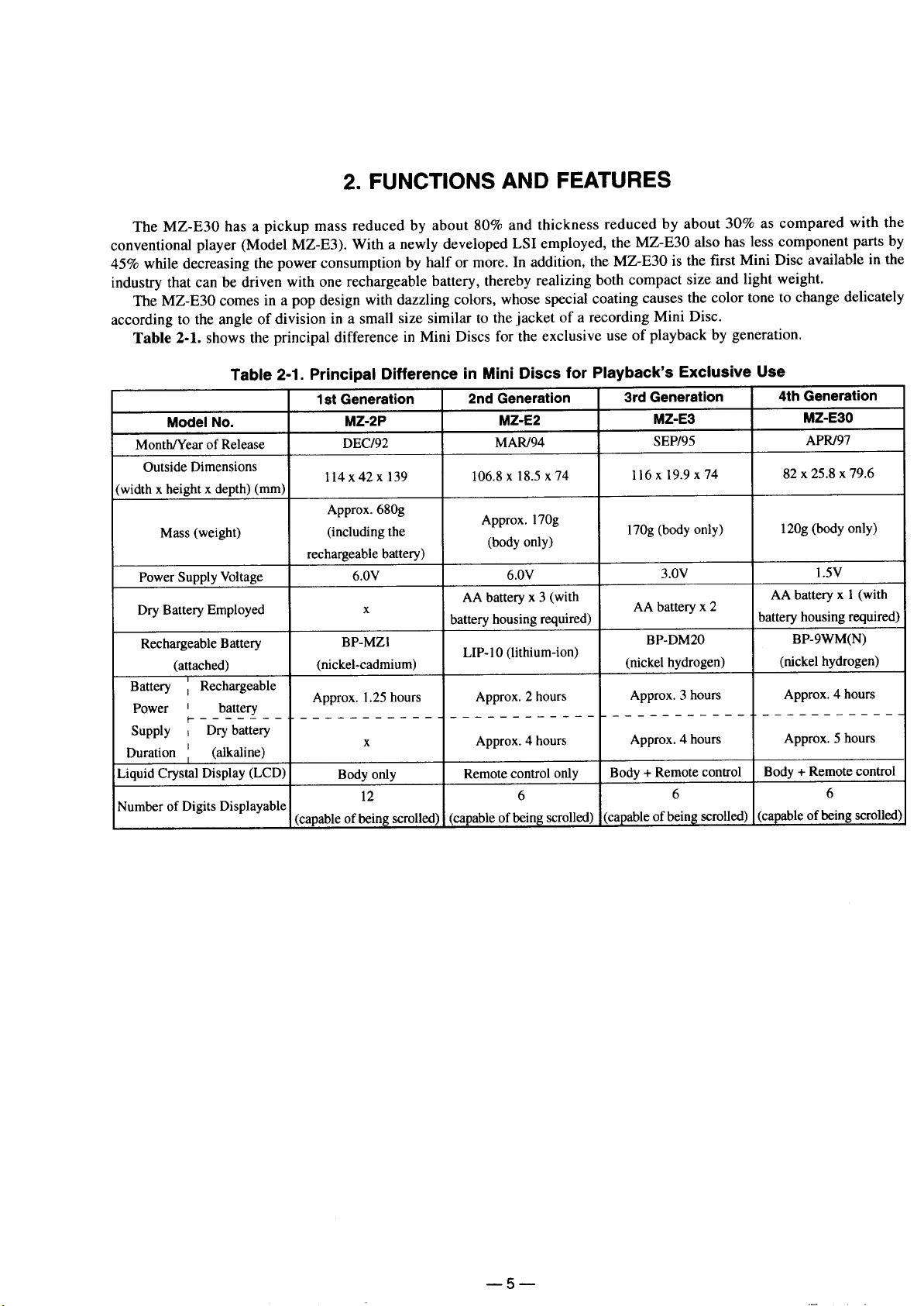
Page 5
Page 6
Page 7
Page 8
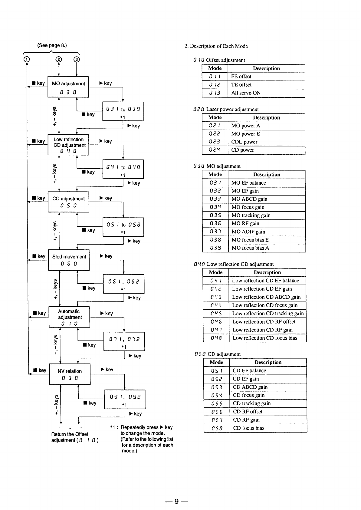
Page 9
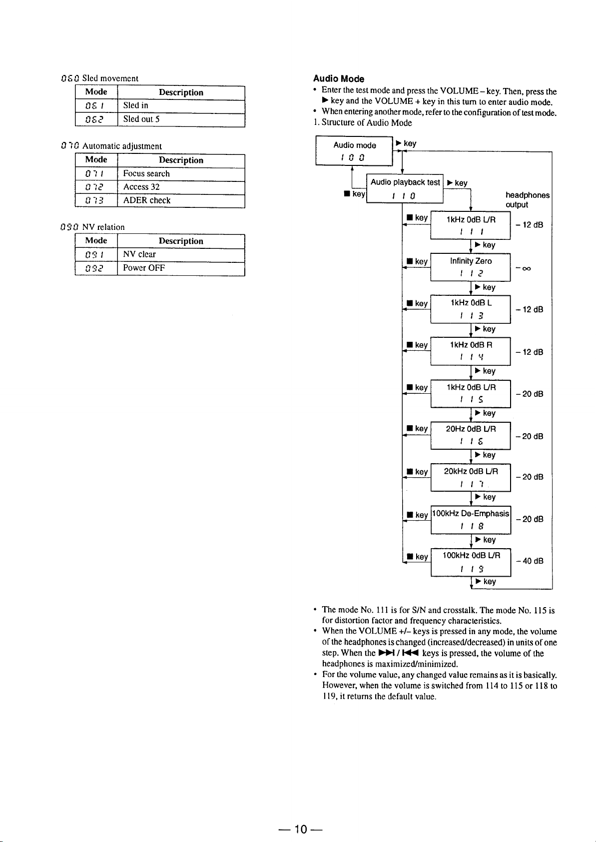
Page 10
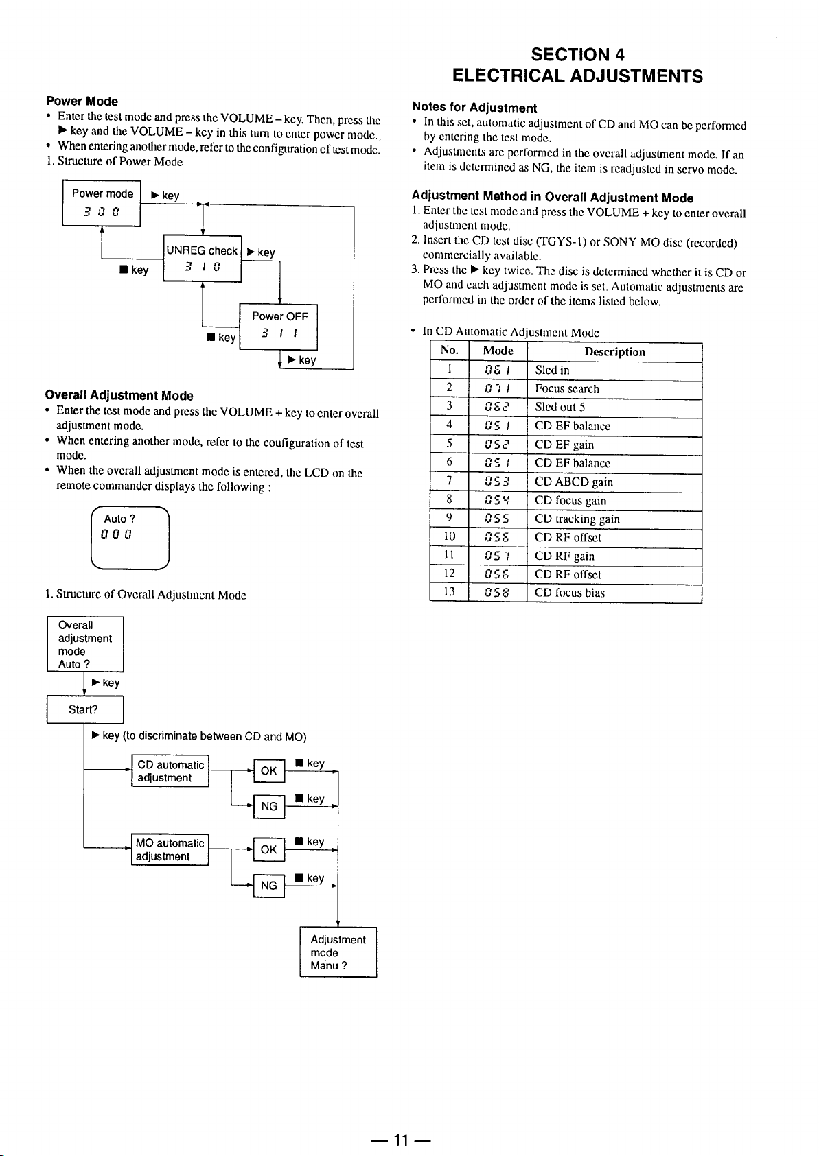
Page 11
Page 12
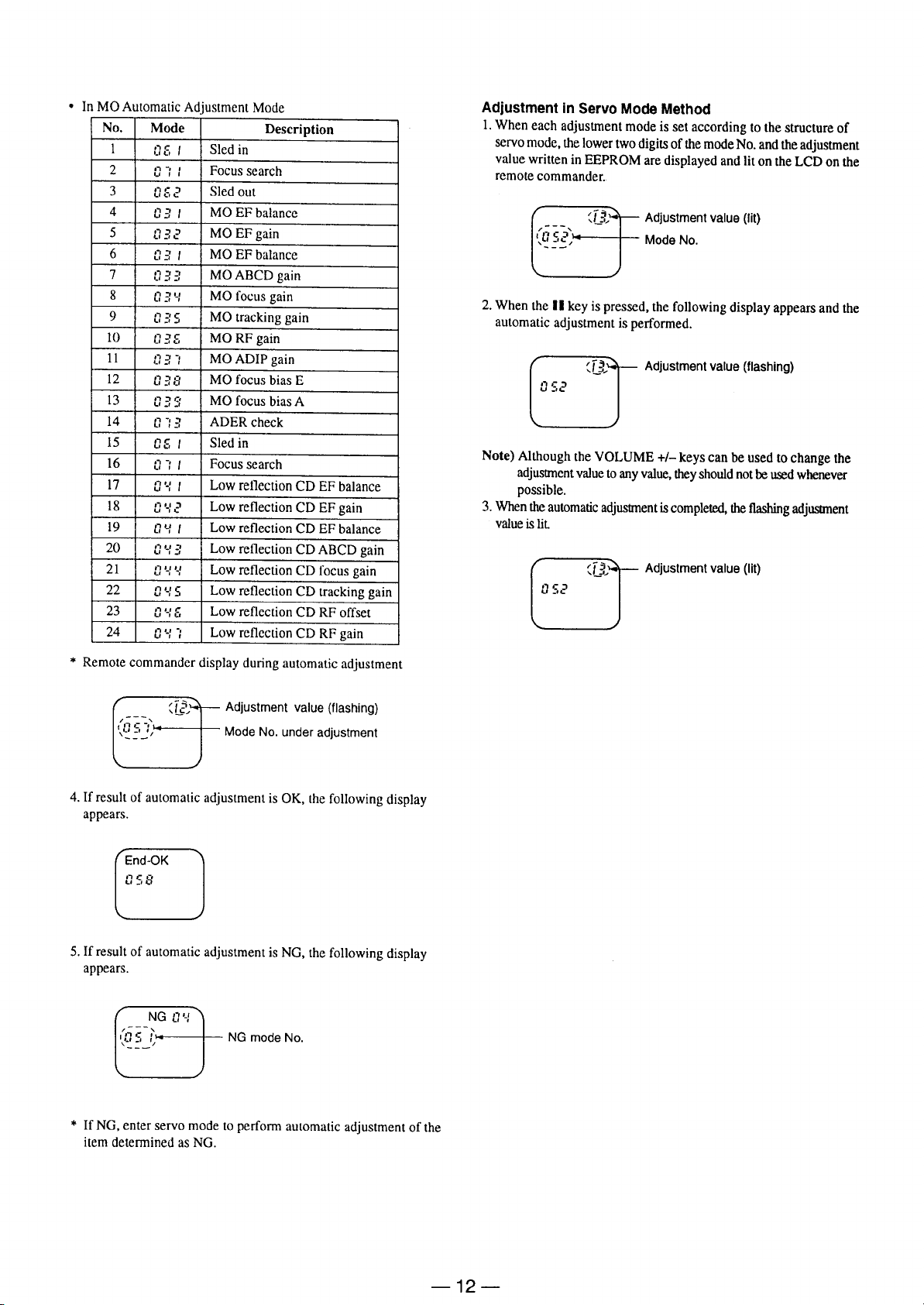
Page 13
Page 14
Page 15
Page 16
Page 17
NEW TECHNICAL THEORY
FOR SERVICING
MZ-E30
OPERATION MANUAL
— 1 —
PORTABLE MINI DISC PLAYER
Page 18

TABLE OF CONTENTS
Section Title Page
1. DIAGRAMS
1-1. BLOCK DIAGRAM ........................................................................................................................................ 3
2. FUNCTIONS AND FEATURES
2-1. Principal Features ............................................................................................................................................. 6
3. Difference in System Configurations by Generation
3-1. System Block Diagrams................................................................................................................................... 8
4. OUTLINE OF SYSTEM
4-1. Microprocessor Interface ................................................................................................................................. 11
4-2. Clock System.................................................................................................................................................... 14
5. POWER SUPPLY CIRCUIT
5-1. Outline of Power supply Circuit Operation .................................................................................................... 16
5-2. Operation in Wakeup (Startup) Mode ............................................................................................................. 20
5-3. Operation in the Sleep (Pause) Mode .............................................................................................................. 24
5-4. Detecting Decrease in Voltage ........................................................................................................................ 24
5-5. RESET Circuit.................................................................................................................................................. 26
6. SYSTEM CONTROL
6-1. Detection Switch .................................................................................................................................................. 27
6-2. Key Input Detection of Control Buttons ......................................................................................................... 28
6-3. Control of APC Circuit and Laser Power ....................................................................................................... 30
7. Playback Circuit
7-1. Outline of Playback Circuit ............................................................................................................................. 32
7-2. Playback Operations......................................................................................................................................... 32
7-3. Digital DBB and Mute Circuit ........................................................................................................................ 33
8. Servo Circuit
8-1. Outline of Servo Circuit ................................................................................................................................... 39
8-2. Intermittent Operations of Servo ........................................................................................... .......................... 40
8-3. Focus Search and Disc Discrimination ........................................................................................................... 40
8-4. Focus Servo Circuit.......................................................................................................................................... 42
8-5. Tracking Servo Circuit..................................................................................................................................... 46
8-6. Sled Servo Circuit ............................................................................................................................................ 46
8-7. Spindle Servo Circuit ....................................................................................................................................... 50
9. Operations of Mechanism ............................................................................................ 53
10. Appendix (Semiconductor Specifications)
10-1. RF AMP SN761050A ...................................................................................................................................... 54
10-2. DSP/Digital Servo µPD63730GC.................................................................................................................... 58
10-3. Servo Driver MPC17A55FTA ......................................................................................................................... 63
10-4. DC-DC Converter MPC1830VMEL ............................................................................................................... 71
— 2 —
Page 19
Page 20
Page 21

3. DIFFERENCE IN SYSTEM CONFIGURATIONS BY GENERATION
For a Mini Disc of playback type, each system is composed of such principal LSIs as shown in Table 3-1.. The difference
between the first and second generations lies in the L/Rch, two pieces of which have been employed in the ATRAC decoder
of the first generation and are intensified into a single LSI in the second generation. The third generation, moreover, has had
the principal LSIs intensified into three pieces except for the servo driver as shown in the table.
In the fourth generation, on the other hand, has been far larger sized and more highly integrated. As a result, the principal
circuit of a Mini Disc has been intensified into a single LSI while six LSIs, including the ATRAC decoder, were employed in
the first generation.
In the case of a playback type model heretofore available, a playback circuit and a decoder circuit have been employed while
jointly using the principal LSI with a recorder/playback unit. The MZ-E30, however, employs an newly developed LSI for the
exclusive use of playback, which has especially main functions, such as shock-proof, ATRAC decoding, EFM decoding and
ACIRC decoding.
The principal LSI in the fourth generation are outlined below.
µPD63730GC : DSSP (digital servo): EFM decoder, ACIR decoder, DRAM controller, ADIP decoder, and clock generator
circuit
MPC17A55FTA : Servo drive circuit, and step up/down power supply circuit
SN761050A : RF amplifier, and I-V amplifier with a gain adjustment switch
Table 3-1. Principal LSIs Employed in a Mini Disc for Playback
Applicable Model
Circuit Block
ATRAC Decoder
Shock-proof Memory Controller
EFM ACRIC Decoder
ADIP Demodulator
Servo Signal Processor
Servo Driver
RF Amplifier
1st Generation
MZ-2P
CXD2527R(2)
CXD2526Q
CXD2525R
CXA1380N
CXA1602R
MPC1718PU
CXA1381R
2nd Generation
MZ-E2
CXD2531AR
CXD2526AR
CXD2525R
CXA1380N
CXA1602R
MPC1718PU
CXA1861R
3rd Generation
MZ-E3
MZ-E40
CXD2536R
CXD2535BR
MPC17A38VM
CXA1981AR
4th Generation
MZ-E30
µPD63730GC
MPC17A55FTA
SN761050A
— 7 —
Page 22
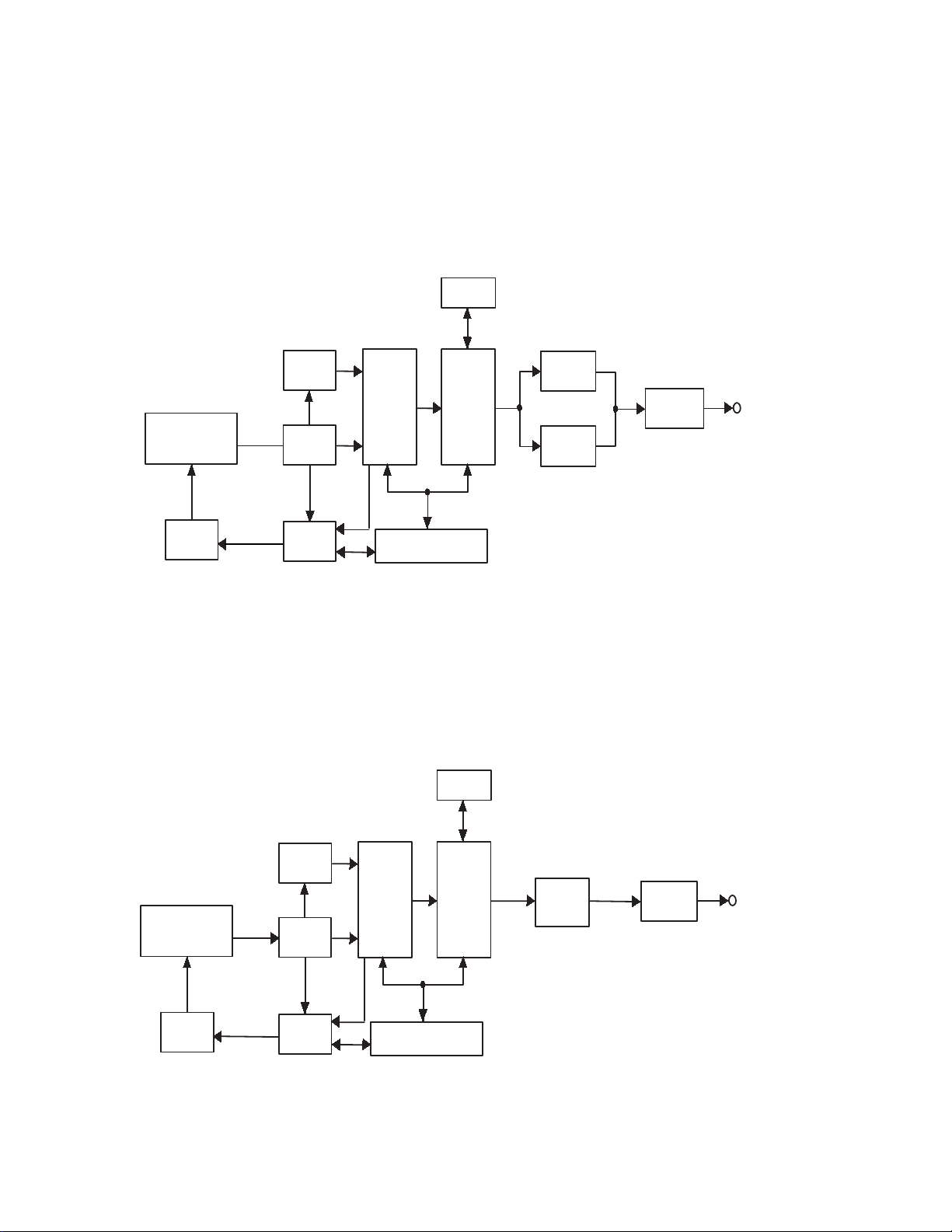
3-1. System Block Diagrams
The playback type Mini Discs belonging to the first thru 4th generations have their respective systems composed of the
blocks illustrated below.
(1) 1st Generation [MZ-2P]
4M DRAM
OPTICAL BLOCK
KMS-130
DRIVE
MPC1718
Fig. 3-1. First Generation Mini Disc System Block Diagram
(2) 2nd Generation [MZ-E2]
ADIP
CXA1380
RF AMP.
CXA1381
SERVO
CXA1602
EFM
ACIRC
CXD2525
SYSTEM CONTROLLER
CXD2526
4M DRAM
SHOCK
PROOF
ATRAC(L)
CXD2527
ATRAC(R)
CXD2527
D/A CONV.
AK4501
AUDIO
OUTPUT
OPTICAL BLOCK
KMS-200
DRIVE
MPC1718
ADIP
CXA1380
RF AMP.
CXA1381
SERVO
CXA1602
EFM
ACIRC
CXD2525
SYSTEM CONTROLLER
SHOCK
PROOF
CXD2526
ATRAC
CXD2531
D/A CONV.
Fig. 3-2. 2nd Generation Mini Disc System Block Diagram
— 8 —
SM5853
AUDIO
OUTPUT
Page 23

(3) 3rd Generation [MZ-E3/E40]
4M DRAM
OPTICAL BLOCK
KMS-201
DRIVE
MPC17A38
Fig. 3-3. 3rd Generation Mini Disc System Block Diagram
(4) 4th Generation [MZ-E30]
RF AMP.
CXA1981
EFM
ACIRC
&
DIGITAL
SERVO
CXD2535
SYSTEM CONTROLLER
CXD2536
4M DRAM
SHOCK
PROOF
&
ATRAC
D/A CONV.
CS4330
AUDIO
OUTPUT
OPTICAL BLOCK
ODX-01
DRIVE
MPC17A55
RF AMP.
SN761050
EFM,ACIRC
SHOCK PLOOF
ATRAC
DIGITAL SERVO
µPD63730
SYSTEM CONTROLLER
D/A CONV.
AK4314
AUDIO
OUTPUT
Fig. 3-4. 4th Generation Mini Disc System Block Diagram
— 9 —
Page 24

4. OUTLINE OF SYSTEM
IC602
4M DRAM
OPTICAL
PICK-UP
IC501
• ERROR AMP
• APC CIRCUIT
REMOTE CONTROLLER
UNIT
LCD
KEY
IC551(1/2)
SERVO DRIVER
POWER SUPPLY
1.5[V]
RF AMP
ERROR SIGNAL
CONTROL SIGNAL
IC901
CONVERTER
EFM SIGNAL
DC-DC
8[V]
2.8[V]
2.5[V]
IC601
DSP/DIGITAL SERVO
• ATRAC DECODER
• RAM CONTROLLER
• ACIRC DECODER
• EFM DEMODURATOR
• DIGITAL SERVO PROCESSOR
IC801
CONTROL
SYSTEM CONTROLLER
• CONTROL THE WHOLE SYSTEM
• LCD DRIVER
• CONTROL THE RF AMP. IC
• CONTROL THE DSP IC
LCD
SIGNAL
EEPROM
IC802
DA DATA
IC301
D/A CONVERTER
SERVO DRIVER
IC803
SLED MOTOR
CONTROL
IC551(2/2)
L/R
FOCUS
TRACKING
SPINDLE
SLED
IC302
H.P.
AMP
L/R
AUDIO OUTPUT
FOCUS/TRACKING
SERVO COIL
SPINDLE
M
MOTOR
SLED
M
MOTOR
Fig. 4-1. General System Block Diagram
Fig. 4-1. is the general system block diagram. The MZ-E30 belonging to the fourth generation is generally composed of the
system controller (IC801) to control the system as a whole as illustrated in the figure. In addition, a digital signal processor and
a digital servo system are mainly composed of the DSP/digital servo LSI µPD63730GC (IC601) for playback.
Other main system components, moreover, include the servo driver (IC551) and RF amplifier (IC501), in which a power
supply circuit is also included.
The DSP/digital servo µPD63730GC for playback is provided with most of those functions which are required for a Mini
Disc to play back, such as ATRAC decoder, EFM decoder, ACIRC decoder, ADIP decoder, DRAM controller, etc. In
addition, it comprises the digital servo (DSSP) and clock generator circuits. Built in the RF amplifier, moreover, are such
circuits as the I-V converter amplifier capable of setting a gain, based on the serial data from the system controller, including
a servo error extractor circuit, an APC circuit and so on.
The D/A converter (IC301) is of the low-voltage 1-bit type, in which a digital de-emphasize function is built, in addition
to the digital filter applicable to 8-multiple oversampling and to a digital Dynamic Bass Boost (DBB). And the headphone
amplifier (IC302) employed in the next stage is of low-power consumption type in which a mute function is incorporated.
The system controller serves to control the RF amplifier and the power supply circuit while processing a digital signal and
controlling the digital servo, together with the DSP/digital servo. In addition, functions to detect a key-in and a remote control
signal, and to control and drive the LCD are also available. The memory (IC802) connected to the system controller is an EEP
ROM (nonvolatile memory) to store mainly servo-system data, such as a traverse supplementary value in the adjustment
(overall regulation) mode, a focus bias, etc. Stored in this memory are the sound volume data just before the power supply
enters the sleep mode, and the stop position address data to be used in the resume function. These data are transferred to each
circuit upon startup.
— 10 —
Page 25

4-1. Microprocessor Interface
IC501 RF AMP
IC601 DSP/DIGITAL SERVO
SSB I/F
21
SBUS
IC802 EEPROM
SSB I/F
22
SCK
4
3
2
1
SBUS CLOCK
SBUS DATA
DODINVDI
SK
NVCLK
CS
NVDO
NVCS
73
72
74
75
323133
CLK
SBUS
SBUS CLK
SBUS DATA
35
34
SINTDSP SINT
27
IC801
SYSTEM CONTROLLER
62
RMC DTCLK
Fig. 4-2. Outline of Microprocessor Interface
J301
REMOTE CONTROLLER
UNIT
4
3
2
1
RM-MZE50
LCD CONTROLLER
The MZ-E30 has a microprocessor interface outlined in Fig. 4-2.. As shown in the figure, the system controller (IC801) is
employed as the mainstay to control the system as a whole. Besides, the DSP/digital servo (IC601) and the EEP ROM (IC802)
are provided. Commands and data are, moreover, bilaterally given and taken to and from the remote commander. In addition,
data are unilaterally transmitted to the RF amplifier. Communications with the DSP/digital servo and RF amplifier, meanwhile,
are performed by way of a serial bus (SBUS). Given and taken between system controller and DSP/digital servo mainly as
described below, furthermore, are those serial data and serial commands which will be input and output to and from Pin #∞
(SBUS DATA) as timed with the serial clock output from Pin #¢ [SBUS CLK].
System Controller n DSP/digital servo (WRITE mode)
• Various function data in each digital servo (DSSP) and
• SERVO- and PLL-mode setting data, and electronic volume setting data
DSP/digital servo n System Controller (READ mode)
• Error data in each servo and
• SubQ/ADIP cluster and sector information
From the system controller to the RF amplifier, SBUS data are transferred similarly to the case of DSP/digital servo. And
the clock line is used to set a gain in the I-V converter amplifier and ADIP extractor circuits located inside the RF amplifier,
to adjust the balance of focus and tracking amplifiers, to amplify the RF, with pit or MO played back, and to select the servo
amplifier polarity.
— 11 —
Page 26

Between the system controller and the EEP ROM, a traverse supplementary value and a focus bias, both obtainable in the
adjustment mode as already referred to, including such data as an offset value of focus/tracking gain, are transferred to and
stored in the EEP ROM synchronously with the clock output from Pin &¢ [NV CLK] of the system controller.
In the conventional model, moreover, the sound volume setting data and the address data relating to the stop position applied
in the resume function are held in the RAM located in the interior of the system controller normally powered. In the MZ-E30,
however, the power will stop being supplied to the system controller if the stop mode should last for about 10 second (which
varies with an optical block position and/or with a mode) for the purpose of saving the energy. These data, therefore, are stored
in the EEP ROM similarly to the servo system data so that they will be read out onto the system controller upon startup and
transferred to each circuit.
Between the system controller and the remote commander, on the other hand, such display information as characters, etc.
are transmitted by way of the remote jack (J301) to the LCD controller located inside the remote commander. Such
information, moreover, is transmitted from the controller inside the remote commander to the system controller since the
receiving data differ in transmission rate, etc. by type of remote control.
To transmit data, the clock timed with such data is also transmitted normally at a time. In the MZ-E30, however, clock
information, etc. are previously transmitted, based on which the controller in the interior of remote control has a function of
generating a clock. Only a single line for data, therefore, permits them to be received.
SBUS Data Transmission Timing
(1) Writing in DSP/digital servo or RF Amplifier from System Controller
To write in the DSP/digital servo or RF amplifier, each bit data are input synchronously with the falling edge of a serial
clock (SCK) as shown in Fig. 4-3.. As shown in the figure, the first three bits relate to the control, with Bit 1 “ST” standing
the for start bit, and Bit 2 “R/W” for the Read or Write mode.
Three types of information, command, address and data, are transferred from the system controller to the DSP/digital servo.
To identify them, Bit 3 “D/C” should be used.
Commands and data, moreover, have a configuration as shown in Fig. 4-4.. When the code of a device coincides with that
of a DSP/digital servo or of an RF amplifier, the device under the same code will receive the related command, thereby
performing subsequent data communications. The instruction code, meanwhile, is used to transfer a command, such as to reset
the hardware.
Fig. 4-3. Timing of Writing in DSP/digital servo or RF Amplifier from System Controller
Fig. 4-4. Command and Data Configurations
— 12 —
Page 27

(2) Reading onto System Controller from DSP/Digital Servo
To read from the DSP/digital servo, the information transferred to the system controller is limited to data only but free from
Bit 3 “D/C” as shown in Fig. 4-5.. The DSP/digital servo has an SBUS terminal employed as an output port only during the
bit period for which data are being output. In any other section, the DSP/digital servo has high impedance.
Fig. 4-5. Timing of Reading onto System Controller from DSP/digital servo
— 13 —
Page 28

4-2. Clock System
IC601
DSP/DIGITAL SERVO
(48fs)
MCK
IC803
SLED MOTOR
19
CONTROL
from RF AMP IC501
37
pin RF-OUT
EFM/ACIRC
DECODER
(96fs)
EFM
PLL
RF
3
ADC
(4fs)
RAM
CONTROLLER
TIMING
GENERATOR
48
25
XI
CLK CK176
28
IC901
DC-DC CONVERTER
IC301
D/A CONVERTER
(48fs)
BCK
41
LRCK
39
(fs)
(384fs)
LRCK
BCK
7
9
6
5 4
XTI
X301
(384fs)
XTO
NOTE : fs = 44.1[kHz]
CLKO
IC801
SYSTEM CONTROLLER
20
MCK
(384fs)
Fig. 4-6. Clock System Block Diagram
Fig. 4-6. shows a block diagram of the clock system.
For the master clock of both system controller (IC801) and DSP/digital servo (IC601), 384 fs (fs = 44.1kHz) available at
X301 connected between Pin 5 [XT1] and Pin 4 [XT0] in the D/A converter (IC301) is supplied from Pin 6 [CLK0].
The timing generator located in the interior of the DSP/digital servo divides a frequency of 384 fs input at Pin $• [X1] so
as to output 48 fs (bit clock) from Pin $¡ [BCK], fs (L/R clock) from Pin #ª [LRCK] and 4 fs from Pin @∞ [CK176].
Based on a frequency of 96 fs from the timing generator, the EFM PLL unit generates a PLL clock (PLCK) so as to
perform EFM demodulation in a subsequent stage of the EFM decoder.
A frequency of 48 fs (bit clock) supplied to Pin !ª [MCK] in the sled motor control (IC803) is used as the master clock for
the controller located inside. And the bit clock (BCK) and L/R clock (LRCK), both output to the D/A converter, are used as
the timing signal for the audio data output from the ATRAC block in the DSP/digital servo. (For details, refer to 7-2. Playback
Operations.)
A frequency of 4 fs, which is output from Pin @∞ [CK176] in the DSP/digital servo to Pin @• [CLK] in the DC-DC converter is
used as a switching signal to drive the STEP-UP circuit in the power supply unit. (For details, refer to 5-1. Outline of Power supply
Circuit Operations.)
— 14 —
Page 29

5. POWER SUPPLY CIRCUIT
Fig. 5-1. shows an outline of the power supply circuit employed in the MZ-E30, as shown in the figure, the power supply
voltages applied to the MZ-E30 may be divided, if roughly classified, into three: 1.5V, 2.8V and 2.5V lines. 2.8V (VC) is
obtained by raising the 1.5V voltage in the step up circuit (2) and supplied to principal circuits, such as D/A converter (IC301),
including system controller (IC801) and DSP/digital servo (IC601).
A voltage of 8V obtained in the step up circuit (1) and in the charge pump circuit, moreover, is supplied to the servo driver
(IC551) and 2.5V to the RF amplifier (IC501) and to the optical block.
To save the electric power, the MZ-E30 has the step up circuits stop operating according to the sleep signal which the
system controller will output if the STOP mode should last for about 10 seconds (which varies with an optical block position
and/or with a mode). As a result, the power will also stop being supplied to each component. To startup, on the other hand, a
wakeup circuit will start up when a operation button located in the remote commander or in the unit is pressed. This will cause
the step up circuit to start operating so that the power is supplied to each component. In addition, this power-saving feature
also interlocks with the ON/OFF operations of the disc door opening/closing detector switch. The power supply then enters the
wakeup (startup) or sleep (standby) mode immediately.
1.5[V]
IC901
CHARGE
PUMP
IC551
2.5[V]
REG
from
SYSTEM CONTROLLER (IC801)
8[V]
2.8[V](VC)
2.5[V]
1.5[V]
IC901
SW
IC901
STEP UP
CIRCUIT(1)
IC551
STEP UP
CIRCUIT(2)
DC-DC CONVERTER
SLEEP SIGNAL
Fig. 5-1. Outline of Power Supply Circuit
SERVO DRIVER(IC551)
HEADPHONE AMP(IC302)
SERVO DRIVER(IC551)
SYSTEM CONTROLLER(IC801)
DSP/DIGITAL SERVO(IC601)
D/A CONVERTER(IC301)
HEADPHONE AMP(IC302)
RF AMP(IC501)
OPTICAL BLOCK
RF AMP(IC501)
— 15 —
Page 30

5-1. Outline of Power supply Circuit Operation
Fig. 5-2. shows the power supply circuit block diagram and timing of waveforms in wakeup (startup) and sleep (standby)
modes.
Operating a key on the unit or in the remote commander connected to Pin #∞ [XWK1] thru Pin #™ [XWK4] in the DC-DC
converter (IC901) will cause the related input pin to become “L,” thereby causing the system control (wakeup/sleep control)
circuit inside to start up.
This will also cause the internal oscillator (OSC1) in the same IC, the step up circuit (1), and the charge pump circuit to start
operating. Subsequently, the internal
oscillator (OSC2) will also begin to operate. As a result, a switching PWM wave of about 200 kHz is output from Pin @™
[PWM1], and a switching power control mode signal from Pin @¡ [DI]. This will cause the step up circuit (2) inside the servo
driver (IC551) to start operating. In addition, the power switch (connected between Pins 4, 5 and 2, 3) will also turn on.
Thus, 2.8V (VC) will be supplied to each component.
At the same time, a voltage of 2.5V output from the 2.5V REG circuit in the interior is supplied from Pin ^¢ [VREG] to the
optical block and to the RF amplifier (IC501).
With 2.8V (VC) applied to Pin [10] [VC] in the DC-DC converter, a RESET signal 6 is sent from Pin 8 [XRST], thereby
causing each IC to start operating. The frequency of 176 kHz (4 fs : fs = 44.1 kHz) obtained, with a frequency of 384 fs
available at X301 divided by 96, enters Pin @• [CLK] from the DSP/digital servo (IC601). Thus, a switching operation continues so
that the step up circuits (1) and (2) will have their respective Drives OSC1 and OSC2 switched over to an external clock (4 fs).
If the voltage of 2.8V (VC) fluctuates, the saw-toothed generator (SAW) inside the DC-DC converter compares the sawtoothed wave obtained from the external clock (4 fs) with the VC input in Pin !º. The generator will control the duty ratio of
a PWM wave output from Pin @™, thereby controlling 2.8V (VC).
The latch clear signal 7, which is input from Pin !• [XWK CLR] in the system controller to Pin #¡ [FF CLR] in the DCDC converter, will have “L” input in either one of XWK1 thru 4 according to an FF (flip-flop) RESET signal inside the system
control in the DC-DC converter. All other input circuits are prohibited from being set until the latch clear signal has become
“H” after setting the FF.
To switch over to the sleep mode, on the other hand, the sleep signal 8 is output from Pin !ª [SLEEP] in the system controller
once the STOP mode has lasted for about 10 seconds (which vary with the optical block position and/or with a mode) or immediately
after the door has opened. This will cause the step up circuits (1) and (2) to stop operating while ceasing to supply the power to each
component.
— 16 —
Page 31

Page 32

Page 33

Page 34

5-4. Detecting Decrease in Voltage
Fig. 5-6. shows a block diagram of the battery voltage monitor circuit. When Pin @§ [UREG CHK CON] in the system controller
becomes to “H,” the VOLT CHECK (Q801) turns on. This will cause the voltage at both ends of the battery to be divided or halved
in the R801 and R802. And the voltage so halved is input to Pin 2 [UREG MON] in the system controller, thereby detecting a
decrease in voltage. A battery voltage of 0.8V or less will cause the MZ-E30 to be put into the STOP mode, with Message
“LoBATT” blinking on the remote commander display. In approximately 5 seconds, a sleep signal will be output from Pin !ª
[SLEEP] in the system controller so that the power supply circuit will stop operating. Upon wakeup, meanwhile, Pin @§ in the system
controller will change from “L” to “H” at the timing shown.
1
UREG MON
VC
VDD
22,50,76
2
from SERVO DRIVER IC551
, pin VB1
32
Q801
VOLT CHECK
R801
47k
1.5[V]
R802
1
2.8[V](VC)
2
UREG CHK CON
Q802
47k
2
UREG CHK CON
0
0
2.7[V]
8.5[ms]
SYSTEM CONTROLLER
26
IC801
19
SLEEP
Fig. 5-6. Battery Voltage Monitor Circuit
TO DC-DC CONVERTER IC901
30
pin SLEEP
— 25 —
Page 35

5-5. RESET Circuit
Fig. 5-7. shows the RESET circuit and the RESET signal timing. The 2.8V (VC) obtained in the step up power supply
circuit of the motor driver (IC551) enters the RESET circuit after being divided with a resistor inside via Pin 0 [VC] in the
DC-DC converter (IC901). In the RESET circuit, the capacitor connected to Pin 7 [CRST] outputs the RESET signal from
Pin 8 [XRST] to main ICs, such as system controller (IC801) and DSP/digital servo (IC601), at the delayed timing shown in
the figure.
2.8[V]
1
VC
from SERVO DRIVER IC551
, pin VB1
32
0
IC901
VC
10
DC-DC CONVERTER
RESET
1
7
GND
CRST
C903
XRST
8
SYSTEM CONTROLLER
1
2
RESET
0
2
XRESET
9
IC801
DSP/DIGITAL SERVO
RESET
30
IC601
6[ms]
2.7[V]
D/A CONVERTER
PD
3
IC301
RESET
24
IC501
RF AMP
PE
7
IC802
EEPROM
Fig. 5-7. RESET Circuit and RESET Signal Timing
— 26 —
Page 36

6. SYSTEM CONTROL
6-1. Detection Switch
Fig. 6-1. shows the detection switches connected to the system controller (IC801) and switch matrix for differentiating the
mode. This unit comes without the part enclosed in the dotted lines in (a) of the same figure which were provided with the
3rd generation unit, namely LIMITIN (detects the innermost circumference of the optical block), REFLECT (detects the
reflectivity rate of the disc), and the switches for differentiating and detecting the battery. Due to the omission of these parts,
focus search after disc replacement, etc. is performed at other than the innermost circumference in this unit. When the servo
turns ON, and data can be read from the disc, TOC accessing is performed based on the address.
Moreover, the differentiation of the MO or playback only disc which was performed by the reflectance rate detection switch
is performed in this unit by alternately switching the internal gain and laser power settings of the RF amplifier during focus
search, and detecting at which of these settings the focus turns ON.
(Details of differentiation of the disc are provided in 8-3. Focus Search and Disc Differentiation.)
As this unit uses a single voltage and does not have a recharge function, it is not mounted with a switch for differentiating and
detecting the battery.
At the ON and OFF of the open/close switch (S801), the wakeup (startup) and sleep (standby) operations of the power supply
are controlled, and at the same time, clearing of the address data of the stop position used by the resume function is performed.
IC801
SYSTEM CONTROLLER
13
54
AVLS
14
OPEN/CLOSE
9
82
15
HOLD
INSL
REFLCT
AM3/NI
PLAY
KEY0
KEY1
55
57
49
SWITCH
MATRIX
PLAY
REMOTE CONTROLLER
UNIT
(SWITCH MATRIX)
HOLD
AVLS
OPEN/CLOSE
INLIMIT
REFLECT
AM3/NI DET
(a) Example of MZ-E3
IC801
SYSTEM CONTROLLER
14
29
6
HOLD SW
AVLS SW
OPN/CLS SW
PLAY
KEY
SET
KEY
RMC
KEY
5
8
7
SWITCH
MATRIX
PLAY
REMOTE CONTROLLER
UNIT
(SWITCH MATRIX)
S802
S805
S801
HOLD
AVLS
OPEN/CLOSE
(b) MZ-E30
Fig. 6-1. Detection Switch Connected to System Controller
— 27 —
Page 37

6-2. Key Input Detection of Operation Buttons
The operation buttons on the unit and remote commander are each composed of switch matrix by combining with the
dividing resistor. As shown in Fig. 6-1. (b), when a operation button on the unit or a operation button on the remote control
unit is pressed, the voltage corresponding to the mode determined by the dividing resistor is input to Pin 8 [SET KEY] or Pin
7 [REM KEY] of the system controller (IC801) respectively. The system controller differentiates the mode according to this
input voltage, and sets the corresponding mode. As no power is supplied to the system controller in the sleep (standby) mode,
it will differentiate the mode after a button is pressed and power is supplied.
(1) When operating using the unit
Fig. 6-2. shows the connection between the operation buttons on the unit and the system controller (IC801) while Table 6-
1. shows the voltage input to the key input Pin 8 [SET KEY] of the system controller when a operation button is pressed.
When power supply to each part starts after wake-up, 2.8V (VC) from Pin #§ [VSTB] is supplied to R808 (47 kΩ) via the
switch inside the DC-DC converter (IC901). When a operation button is pressed in this state, a dividing voltage determined by
R808 (47 kΩ) and the resistor corresponding to that operation button, is input to Pin 8 of the system controller. A separate
line from the switch matrix is incorporated only for the PLAY button and voltage is input separately to Pin 5 [PLAY KEY]
so that the PLAY mode is set even when the button has been pressed instantaneously.
Table 6-1. Key Input Voltage During Operations of
Unit (Reference Values)
2.8[V]
PLAY
STOP
VOL+
P-MODE
REW
FF
VOL-
VC
VC
IC901
DC-DC CONVERTER
10
IC801
SYSTEM CONTROLLER
5
8
R803
470k
36
VSTB
R808
47k
R809 2.2k
R810 4.7k
R811 6.8k
R812 15k
R813 33k
PLAY KEY
SET KEY
Operation Buttons of Unit
STOP
FF
REW
VOL +
VOL –
P-MODE
When nothing is pressed
Pin 8 of IC801
0V
0.15V
0.4V
0.6V
1.0V
1.5V
2.8V
Fig. 6-2 Key Input Circuit of Operation Buttons of Unit
— 28 —
Page 38

(2) When operating using the remote commander
Fig. 6-3. shows the connection between the operation buttons on the remote commander and the system controller (IC801)
while Table 6-2. shows the dividing voltage input to Pin 7 [RMC KEY] of the system controller when a remote commander
button is pressed.
When power supply to each part starts after wake-up, the two switches inside the DC-DC converter turn ON, and the
dividing voltage obtained by R905 (150 kΩ) and R838 (10 kΩ) is input to Pin 7 [RMC KEY] of the system controller. When
a remote commander button is pressed in this state, the matrix resistor corresponding to that button and a dividing voltage and
R905 are connected in parallel form, and the voltage shown in Table 6-2. is input to Pin 7 of the system controller.
Table 6-2. Key Input Voltage During Operations of
Remote Commander (Reference Values)
VC
IC901
DC-DC CONVERTER
2.8[V]
VC
10
36
VSTB
R905
150k
XWK3
33
R838
10k
HOLD
VOL+
VOL-
STOP
PAUSE
PLAY
REW
1k
1.5k
1.3k
2k
1.5k
2.6k
RMC KEY
IC801
SYSTEM CONTROLLER
7
Operation Buttons of
Remote Commander
VOL+
VOL–
STOP
PAUSE
PLAY (FF)
REW
When nothing is pressed
Pin 7 of IC801
1.4V
1.5V
1.65V
1.8V
2.0V
2.5V
0.2V
VRMC
2
1
GND
Fig. 6-3. Key Input Circuit of Remote Commander
— 29 —
Page 39

6-3. operation of APC Circuit and Laser Power
2.8[V](VC)
IC501
RF AMP
LD-VDD
16
R506
4.7
LD-SNS
15
(2.7[V])
Q501
LD-DRV
PD-IN
14
11
3
LD DRIVE
CN501
5
LD
8
2
ILCC
LDGND
-
+
SSB-I/F
+
IC801
PD-O
13
C506
LPF
R883
1
APCREF
41
(2fs)
C806
R504
PD-I
12
SYSTEM CONTROLLER
KGND
7
PD
PD
6
18
VTEMP
21
SBUS
22
SCK
IC801 SYSTEM CONTROLER
1
41
pin APCREF
2
Q501 COLLECTOR
IC501 RF AMP
3
11
pin PD-IN
35
34
SBUS CLK
SBUS DATA
APPROX.4.6[s]
APPROX.1.8[s]
0
0
0
ON ON
2.7[V]
2[V]
750[mV]
OFF
Fig. 6-4. APC Circuit and Waveform Timing
Fig. 6-4. shows the APC (Automatic LASER Power operation) circuit and main waveform timings. The APC circuit
controls the driving current of the laser so that the voltage supplied from outside becomes the same as the monitor diode
voltage. With functions such as PLAY where the laser diode emits light, Pin $¡ [APC REF] of the system controller (IC801)
outputs a 88.1 kHz (2 fs:fs=44.1 kHz) PWM waveform at the waveform timing (1) shown in the figure. In the LPF, the DC
APC REF signal is input to Pin !™ [PD-I] of the RF amplifier (IC501), passed through the two differential amplifiers inside,
output from Pin !¢ [LD-DRV], passed through the LD drive (Q501) to drive the laser diode inside the optical block.
Inside the monitor diode (PD), the photoelectric current corresponding to the amount of radiated laser light is converted to
voltage by the resistor connected between the monitor diode anode and GND, input to Pin !¡ [PD-IN], and fed back to the first
stage amplifier to control the laser power. A constant current circuit is composed by feeding back the voltage decreased by the
R506 resistor (4.7 Ω) connected to the emitter of the LD drive, so that the driving current does not change even when the
power supply voltage changes.
The ON/OFF of the laser driving current is controlled by the system controller via the serial bus (SBUS).
During normal playback, an approximately 1.8 seconds ON and 2.8 seconds OFF are repeated as shown by the timing in the
figure to save power.
— 30 —
Page 40

In models which can record, changes in the recording power of the disc according to the ambient temperature and internal
temperature of the unit are detected by the temperature sensor and compensated. The RF amplifier (IC501) has a function
which converts temperature into voltage and outputs it from Pin !• (VTEMP), but this function is not used in this unit intended
exclusively for playback.
As the optimum read power differs between the playback only disc and MO disc, the disc is differentiated by focus search
performed immediately after the unit is started. The duty ratio of the PWM wave output from Pin $¡ of the system controller
is controlled so that 0.6 mW power is obtained if the disc is a playback only disc, and 0.8 mW power is obtained if it is a MO
disc.
(Details of differentiation of disc are provided in 8-3. Focus Search and Disc Differentiation.)
— 31 —
Page 41

7. PLAYBACK CIRCUIT
7-1. Outline of Playback Circuit
Fig. 7-1. shows the structure of the playback circuit of the Mini Disc. The RF data read by the optical block is demodulated
by the EFM demodulator, and data errors are detected and corrected by the ACIRC decoder.
Since the Mini Disc data has the same structure as the CD-ROM, it is decoded in the CD-ROM decoder in the next step,
and the ATRAC data compressed to approximately 1/5 is stored in the shock proof memory (buffer RAM). Apart from the
ATRAC data, this memory also stores error information (C2PO) and TOC/UTOC information.
The ATRAC data is written in the memory intermittently, and read to the ATRAC decoder periodically. The compressed
data is expanded to 16-bit linear data by the ATRAC decoder, D/A converted by the D/A converter, and output as analog
signal.
MD
EFM
DEMODULATOR
ACIRC
DECODER
CD-ROM
DECODER
SHOCK PROOF
MEMORY
ATRAC
DECODER
D/A
CONVERTER
Fig. 7-1 Structure of Mini Disc (Playback Circuit)
7-2. Playback Operations
Fig. 7-2. shows the block diagram of the playback circuit and the waveform of the main parts.
The two RF signals (I and J signals) I-V converted inside the optical block are input respectively to Pins 6 (VI) and 7
(VJ) of the RF amplifier (IC501). The RF amplifier sets the gain and internal circuits according to the disc type (MO or CD)
using the serial data input form the system controller (IC801).
Disc discrimination and gain setting are performed together during focus search. (Details are provided in 8-3. Focus Search
and Disc Discrimination.)
Furthermore, the output of the RF amplifier (1) is switched according to the disc type written in the TOC. In the case of the
pit area of the playback only disc and MO disc, the additional signal of I and J is output, based on the Vref voltage (0.88V)
generated inside the RF amplifier, from Pin #¶ (RF-OUT) to the DSP/digital servo (IC601) via the RF amplifier (2) and EQ
(equalizer). In the case of the groove area (UTOC, program area) of the MO disc, the subtraction signal is output. (1)
The RF signal is converted to a 7-bit digital value at a sampling frequency of 4.23 MHz (96 fs:fs=44.1 kHz) by the
A/D converter inside the DSP/digital servo. In the EFM PLL circuit, clock extraction and generation are performed, and based
on the channel clock (4.23 MHz) obtained, EFM demodulation is performed in the next stage. In the ACIRC decoder, data
errors are detected and corrected, and the data is then written in the DRAM via the RAM controller. The accumulated data is
compressed to approximately 1/5 according to the transfer command from the system controller, and periodically sent to the
ATRAC decoder block. In the ATRAC decoder block, the compressed data is expanded, and the data is output continuously
to the D/A converter (IC301) from Rch and Lch alternately in synchronization with LRCK (L/R clock) and BCK (bit clock)
at the timing of the audio signal shown in the figure.(Refer to 2 to 4.)
— 32 —
Page 42

The D/A converter is also incorporated with a digital DBB (Dynamic Bass Boost) and eight times over sampling digital
filter. These perform boosting of low bands and data filtering respectively using digital signals. The D/A converter also has a
deemphasis function, which is controlled using the emphasis ON and OFF signals output from Pin #• (EMP) of the DSP/
digital servo. The D/A converted analog signal is output to the headphone amplifier (IC302) via the VOLUME DOWN circuit
(Q301), which attenuates the audio signal boosted when DBB is ON, from Pins !¶ and !§ (A OUT L, AOUT R).
When the VOL button connected to the system controller is operated to control volume, the volume data is sent to the
ATRAC decoder block of the DSP/digital servo (IC601) via the serial bus (SBUS) and the volume is controlled by digital
signal processing inside the block.
Likewise for the beep sound when the remote operation button is operated, the data is sent to the DSP/digital servo (IC601),
the beep signal is generated inside the DSP/digital servo and output to the headphone via the D/A converter and headphone
amplifier.
7-3. Digital DBB and Mute Circuit
Fig. 7-3. shows the digital DBB (Dynamic Bass Boost) and mute circuit.
The D/A converter (IC301) incorporates a digital DBB function which is switched ON/OFF using the DBB switch (S301)
connected to Pin !¡ (DBB0) and Pin !™ (DBB1).
Low bands are boosted using the digital signal.
When Pin !¡ is set to “H”, at the reference level (–12 dB), signal is boosted by about 3.5 dB for 100 Hz. When Pin !™ is set
to “H”, it is boosted by about 8.5 dB. When DBB is turned ON, Q301 connected between the D/A converter and headphone
amplifier (IC301) also is turned ON at the same time. As a result, R206 (15 kΩ) and R202 (6.8 kΩ) or R106 and R102 are
connected in parallel, and attenuate the volume boosted by the DBB to prevent clipping caused by the volume increasing and
excess input to headphone amplifier when the DBB is ON.
On the other hand, the headphone standby signal from Pin &º (HP STBY) or the mute signal from Pin ^ª (HP MUTE) of
the system controller is input to the headphone amplifier to turn the standby mode and mute. When the standby signal is set
to “H” or the mute signal is set to “L” as shown in the timing chart in the figure, the sound signal input from the D/A
converter is output from the headphone.
During wakeup, and immediately after the PLAY mode is set, the headphone is muted by the approximately 500 to 600 ms
mute signal output from the system controller to prevent the output of pop noise, etc.
— 33 —
Page 43

8. SERVO CIRCUIT
8-1. Outline of Servo Circuit
IC551(1/2)
SLED
MOTOR
SERVO DRIVER
FOCUS
TRACKING
IC551(2/2)
SERVO DRIVER
SPINDLE
SLED
M
M
FOCUS
COIL
TRACKING
COIL
SPINDLE
MOTOR
SLED
MOTOR
OPTICAL
PICK-UP
ODX-01
IC501
RF AMP
FE/TE
RF/ADIP
IC601
DSP/
DIGITAL SERVO
IC801
SYSTEM
CONTROLLER
IC802
EEP ROM
IC803
CONTROL
Fig. 8-1 Outline of Servo Circuit
As shown in Fig. 8-1., the servo circuit is composed of the RF amplifier (IC501), DSP/digital servo (IC601), system
controller (IC801), and the servo driver (IC551).
When a playback disc is played, the servo circuit operates in the same way as the CD player.
The focus and tracking servos A/D convert the error signals output from the RF amplifier inside the DSP/digital servo
(IC601), and perform servo calculation and correction. They then convert the signals to 2 fs (fs=44.1 kHz) PWM wave and
output them to drive the focus and tracking coil using the servo driver (IC551).
The spindle servo sends the measured period of the EFM frequency divided signal obtained from the RF signal using the DSP/
digital servo (IC601) to the system controller, generates the spindle error signal inside, and controls the rotation of the spindle
motor via the servo driver. The sled servo A/D converts the tracking error signal, sends the data to the system controller, and
generates the control signal of the sled motor control (IC803). The sled error signal is generated from this control signal in the
sled motor control (IC803) in the next stage, and used to control the rotation of the sled motor via the servo driver.
When the MO disc is played back, only the spindle servo in the servo circuit differs from when the playback only disc is
played back. In the case of the playback of the playback only disc, the measured period of the EFM frequency divided signal
obtained from the RF signal is used. In the case of the MO disc, that of the frequency divided signal obtained from the ADIP
signal recorded in the groove area is used.
In this unit, the digital servo composed of the RF amplifier (IC501), DSP/digital servo (IC601), and system controller
(IC801) controls focus, tracking, sled, and spindle. RF level adjustment and ABCD level adjustment are performed
automatically immediately after the unit is started by pressing the PLAY button so that the optimum values according to the
disc type (CD/MO) can be obtained by the digital servo.
The adjustment values of the servo such as focus/tracking gain, EF balance, focus bias, etc. stored in the non-volatile memory
(IC802, EEPROM) are sent to the servo circuit when the adjustment mode is started to optimize the servo. (Details of the
adjustment mode are provided in 4. Electrical Adjustments in the Service Manual.)
— 39 —
Page 44

8-2. Intermittent Operations of Servo
The focus servo and tracking servo of this unit turn ON and OFF repeatedly during normal playback and operate
intermittently.
To save power, they repeat 1.8 seconds of ON and 2.8 seconds of OFF as shown in the timing chart in Fig. 8-2. along with the
switching of the laser diode to ON/OFF. In the CLV servo, the control is different. When ON, as some time is required for the
servo to stabilize, the disc is rotated continuously in the rough servo mode even when the focus servo and tracking servo are
OFF. When the servo is ON, the focus servo sets the focus based on the focus voltage just before the servo is OFF to operate
the focus servo circuit.
Approx.
Approx.
1.8[s]
2.8[s]
FOCUS SERVO
TRACKING SERVO
ON
ON
OFF
OFF
OFF
ON
CLV SERVO
LOCK LOCK LOCK
LASER DIODE
ON
Fig. 8-2. Intermittent Operations of Servo
8-3. Focus Search and Disc Discrimination
ON
TRK-ON
A
ROUGH SERVO
B
ROUGH SERVO ROUGH SERVO
ON ONOFF OFF
ON
TRK-ON
AA
OFF
B
Y axis shows the focus drive voltage
The top is the disc.
Fig. 8-3. Focus Search (Previous Model)
Compared to the current CD discs, as the reflection rate of the MO disc is low (15 to 30%), the difference between the
pseudo reflected light on the disc surface (polycarbonate board surface of the side where signals are read) and the light
reflected from the MO media side is small, making it difficult for the IC to differentiate between the two. As a result, the FOK
signal sometimes becomes “H” according to the light reflected from the disc surface. Thus when the focus is turned ON, focus
is accidentally imposed on the disc surface. Focus search is therefore performed from near the disc (down search) unlike
current CDs to impose focus. (Part A of Fig. 8-3.)
— 40 —
Page 45

In 4th generation playback only players, improvements of the optical block enabled detection of the MO media to be
performed properly even when search was carried out from the far side of the disc as the disc surface deviated from the
focusing range.
As shown in Fig. 8-4., when search is performed from the side near the disc (down search), a disc with a high reflection rate
(CD) is set, when search is performed from the side far away from the disc (up search), a disc with a low reflection rate (MO)
is set, and MO/CD differentiation is performed together with focus search. After this, the focus on signal generated from the
focus OK signal is used to turn ON the focus and tracking servos.
The following shows the focus search process and disc differentiation method of the 4th generation playback only player.
Focus search process and disc differentiation
(1) After the power is turned ON, first high reflection rate gain of the RF amplifier and laser power of the high reflection rate
disc (CD) is set (0.6 mW), and focus search (from up to down) is started. (Part A of Fig. 8-4.)
(2) If this high reflection rate disc (CD) is loaded, focus is imposed. If a low reflection rate disc (MO) is loaded,
focus is not imposed and the the idling state is set. (Part A of Fig. 8-4.)
(3) Search is performed once, and if the disc is not detected (if idling is set), the RF amplifier sets the low reflection rate gain
again, sets the laser power of the low reflection rate disc (MO) (0.8 mW), and focus search (do wn to top) is performed. (Part
B of Fig. 8-4.)
(4) If focus is imposed here, the disc is determined to be a low reflection rate disc (MO), after which the tracking servo turns ON
and pit/groove differentiation is performed. This is performed by simultaneously switching the I+J (pit) and I-J (groove) of
the RF signal output from the RF amplifier (IC501) and E-F (pit) and F-E (groove) of the tracking error signal using the pit/
groove switching signal and detecting on which side the RF data is read.
(5) When the focus is not imposed (when the ABCD le vel does not reach a certain le vel), the abo ve operation is retried till eight
times.
(6) If focus is still not imposed after the retries, “NO DISC” is displayed.
* Disc differentiation is performed only once after the power is turned ON.
Immediately after the power turns ON, the offset data obtained in the adjustment mode and stored in the non-volatile
memory (IC802, EEPROM) is sent to the servo circuit to perform correction. To correct the offset generated due to
temperature characteristics, etc. of the optical block, fine adjustments of the focus offset and tracking offset are performed each
time the unit is started.
Standby
PON
Offset correction
CLV start
CLV
for
stabilization
Focus search start
ON
TRK-ON
Setting of high
reflection rate
(CD)
A
ON
TRK-ON
Setting of low
reflection rate
(MO)
B
AA
(When high
reflection rate)
“NO” DISC after 8 times of
no disc check continuously
B
(When low
reflection rate)
Y axis is focus drive voltage.
Top is disc
Fig. 8-4 Focus Search and Disc Differentiation (4th Generation Playback Only Player)
— 41 —
Page 46

8-4. Focus Servo Circuit
As shown in Fig. 8-5., the photoelectric current output from the optical block A to D detectors is input to the RF amplifier
(IC501), converted to voltage by the I-V amplifier inside, passed through the ABCD amplifier and F.E. (focus error) amplifier,
and the ABCD signal is output from Pin #∞ (ABCD) while the focus error signal is output from Pin #§ (FE) to the DSP/digital
servo (IC601). The A to D I-V amplifiers each have a gain switch for adjusting level. Using the serial data input from the
system controller (IC801) via the serial bus (SBUS), initial settings of the gain is performed together with ABCD level
adjustment according to the disc type each time PLAY, etc. to obtain the optimum output. To perform these, the system
controller reads the ABCD level data A/D converted from the DSP/digital servo (IC601) and control the gain switch so that the
data becomes the prescribed level.
The input of the DSP/digital servo (IC601) is incorporated with an A/D converter, which converts the ABCD signal and the
FE signal to 7-bit data at sampling frequencies of 22.05 kHz (fs/2) and 88.2 kHz (2 fs) respectively. The focus error signal is
then subject to servo calculation in the DSSP (digital servo signal processor) block, converted to the 88.2 kHz PWM wave, and
used to control the focus coil via the servo driver (IC551) and LPF (low pass filter).
In addition to the ABCD level adjustment mentioned earlier, the A/D converted ABCD signal data is also compared with the
reference level preset with the serial data from the system controller, and the FOK (focus OK) detection signal is output to the
system controller via the serial bus (SBUS).
The focus gain and focus bias adjustments are performed in the adjustment mode, the adjustment values are stored in the nonvolatile memory, the data is sent to the servo circuit via the serial bus (SBUS) at starting to set the focus gain and focus bias
adjustment data. In the case of focus bias, data on the bias amount during adjustment is sent to the DSSP block, added to the
focus error signal, and used to drive the focus coil.
— 42 —
Page 47

Page 48

Page 49

Page 50

Page 51

Internal Block Diagram
OFC-C1
OFC-C2
EQ-1
EQ-2
3941424644
EQ-3
VJ
EXT-IN
6
VI
7
10
IA
9
IB
3
IC
2
ID
1
IE
4
IF
27
i-v
conversion
i-v
conversion
i-v
conversion
i-v
conversion
i-v
conversion
i-v
conversion
RF
ABCD
Focus-Error
ADIP
FE and TE
DFCT
MIRROR
OFTRK
ADIP BPF
T-COUNT
37
26
25
34
35
38
36
29
31
30
32
33
28
FR-OUT
DFCT
OFTRK
OFTIN
ABCD
MIRR-VTH
FE
ADIP
BPFC0
BPFC1
REXT2
TE
T-COUNT
PD-IN
PD-I
PD-O
LD-SNS
LD-DRV
LD-VDD
SBUS
SCK
RESET
DVA1
19
11
12
13
15
14
16
21
22
24
17
APC
Remote control
Thermometer
Power supply
REXT1
18
VTEMP
8
A-VDD
43
A-VDD
20
D-VDD
47
VREF-OUT
46
VREF2-OUT
AGND
5
40
AGND
48
AGND
DGND
23
— 55 —
Page 52

Pin Assignment
MIRR-VTH
EQ-3
AGND
EQ-2
EQ-1
AVDD
OFC-C1
OFC-C2
VREF2-OUT
VREF-OUT
A-GND
48 47 46 45 44 43 42 41 40 39 38 37
RF-OUT
AGND
A-VDD
PD-IN
PD-I
ID
IC
VJ
1IE
2
3
4
IF
5
VI
6
SN761050A
7
8
9
IB
10
IA
11
12
13 14 15 16 17 18 19 20 21 22 23 24
PD-O
LD-DRV
LD-SNS
LD-VDD
DVA1
VTEMP
REXT1
DVDD
SBUS
SCK
DGND
RESET
36 FE
35
34
33
32
31
30
29
28
27
26
25
ABCD
OFTIN
TE
REXT2
BPFC0
BPFC1
ADIP
T-COUNT
EXT-IN
DFCT
OFTRK
— 56 —
Page 53

Pin Function
Pin No.
1
IE
2
ID
3
IC
4
IF
5
AGND
6
VI
7
VJ
8
A-VDD
9
IB
10
IA
11
PD-IN
12
PD-I
13
PD-O
14
LD-DRV
15
LD-SNS
16
LD-VDD
17
DV A1
18
VTEMP
19
REXT1
20
DVDD
21
SBUS
22
SCK
23
DGND
24
RESET
25
OFTRK
26
DFCT
27
EXT-IN
28
T-COUNT
29
ADIP
30
BPFC1
31
BPFC0
32
REXT2
33
TE
34
OFT-IN
35
ABCD
36
FE
37
RF-OUT
38
MIRR-VTH
39
EQ-3
40
AGND
41
EQ-2
42
EQ-1
43
AVDD
44
OFC-C1
45
OFC-C2
46
VREF2-OUT
47
VREF-OUT
48
AGND
Symbol
I/O
I
E current input
I
D current input
I
C current input
I
F current input
—
Analog GND
I
I voltage input
I
J voltage input
—
Analog Vdd
I
B current input
I
A current input
I
PD AMP non-inverted input
I
PD AMP inverted input
O
PD AMP output
O
LD-driver PNP-Tr base output
I
LD current detection input
I
LD power supply voltage detection input
I
Serial device code
O
Temperature gauge output
—
Temperature gauge current source setting resistor
—
Digital Vdd
I
Serial data input
I
Serial clock input
—
Digital GND
I
Reset input
O
Off track detection output
O
Defect detection output
I
External T-COUNT input
O
T-COUNT output
O
ADIP output
—
ADIP-BPF AC connecting capacitor
—
ADIP-BPF AC connecting capacitor
—
ADIP-BPF current source setting resistor
O
Tracking error output
I
Off track detection input
O
A+B+C+D output
O
Focus error output
O
RF output
I
Mirror comparator threshold setting
—
RF-amp phase shifter
—
Analog GND
—
RF-EQ external constant 2
—
RF-EQ external constant 1
—
Analog Vdd
—
DC canceler external capacitor 1
—
DC canceler external capacitor 1
O
Reference voltage output (GND reference 1.2V)
O
Reference voltage output (GND reference 1.2V)
—
Analog GND
Function
— 57 —
Page 54

10-2. DSP/Digital Servo µPD63730GC
DSP/digital servo for MD playback
• Built-in ATRAC decoder for playback
• Digital servo, EFM decoder, and ACIRC decoder functions
5175
76
100
50
uPD63730GC
26
251
— 58 —
Page 55

Internal Block Diagram
DRD 0-3
DRA 0-11
XWE
XWE2
XOE
XOE2
XCAS
XRAS
54
55
60
61
59
63
4
12
X BUSY
34
DREQ
XATWE
ATDT
16
AC-WDCK
S-DATA
8
DRM and peripheral-control
Address-generator
RD-DT-ECC
8
WRREQ etc.
EBA
12
ECC-DATA
8
EFM-DATA-A/B
16
AUDATA
40
8
AC-DATA
BCK
41
39
AC-BYCK
EFM
EMP
LRCK
38
ATRAC
Decoder
Sector
Decoder
AC-LRCK
AC-WDCK
ACIRC
Decoder
D-OUT
43
FLAG
ID0-3
SBR
SBW
SBA
8
SBD
8
SOREQ
2nd MSB
MCK-I/O
47
PMCK
25
44
Clock
Generator
SSB-Control
SubQ/ADIP
Decodeer
CK176
8
Monitor-I/O etc.
4
4
48
49
45
50
30
33
32
31
92
82
81
94
93
XI
XO
MCK/2
MCK
RESET
SINT
SCK
SBUS
TEST
M0CK
M00-3
M1CK
M10-3
ERFLAG
CRCF
FON
FOK
TFOUT
TROUT
FROUT
FFOUT
95
96
21
PLCK
22
23
24
11 12 13 4 6 5 1 3 2 7
DEFECT
T-COUNT
DSSP
OFTRK
TE
FE
FE
ABCD
TE
ABDC
EFM
VDD ADC
EFM
RF
ADC
RF
PLL
VREF
ADIP
ADIP
ADIP
PLL
89
EFM
88
PLCK
91
ADIP-DATA
ADPLCK
90
VSS
VDD
9
VRB
VRT
8
— 59 —
Page 56

Pin Configuration
VDD
DRA3
DRA2
DRA1
DRA0
DRA4
DRA5
DRA6
DRA7
DRA8
DRA10
DRA11
XRAS
DRA9
XOE2
XOE
XCAS
DRD2
DRD3
VSS
XWE2
XWE
DRD1
DRD0
51525354555657585960616263646566676869707172737475
VDD
VSS
MI0
MI1
MI2
MI3
MICK
MOCK
MO0
MO1
MO2
MO3
VDD
PLCK
EFM
ADPLCK
ADIP-DATA
TEST
CRCF
ERFLAG
FON
FOK
ID3
ID2
ID1
ID0
76
77
78
79
80
81
82
83
84
85
86
87
88
89
90
91
92
93
94
95
96
97
98
99
100
VREF
VDD ADC
50 MCK
49
XO
48
XI
47
MCK-I/O
46
VSS
45
MCK/2
PMCK
44
43
DOUT
42
VSS
41
BCK
40
AUDATA
39
LRCK
38
CK176
EMP
37
VDD
36
35
34
XBUSY
33
SINT
32
SCK
31
SBUS
30
RESET
29
VDD
28
27
26
uPD63730GC
25242322212019181716151413121110987654321
FE
ABCD
TE
VRT
ADIP
VRB
VSS ADC
T-COUNT
DEFECT
OFTRK
VSS
TFOUT
TROUT
FROUT
FFOUT
RF
— 60 —
Page 57

Pin Function
Pin No.
1
VDD ADC
2
VREF
3
RF
4
FE
5
ABCD
6
TE
7
ADIP
8
VRT
9
VRB
10
VSS ADC
11
T -COUNT
12
DEFECT
13
OFTRK
14
VSS
15
16
17
18
19
20
21
TFOUT
22
TROUT
23
FROUT
24
FFOUT
25
CK176
26
27
28
29
VDD
30
RESET
31
SBUS
32
SCK
33
SINT
34
XBUSY
35
36
37
VDD
38
EMP
39
LRCK
40
AUDATA
41
BCK
42
VSS
43
DOUT
44
PMCK
45
MCK/2
46
VSS
47
MCK I/O
48
XI
49
XO
50
MCK
Symbol
I/O
—
Power supply for ADC block
I
Reference voltage input
I
RF signal input
I
Focus error input
I
ABCD (all quantity of light) signal input
I
Tracking error input
I
ADIP signal input
I
ADC high potential reference voltage for RF
I
ADC low potential reference voltage for other than RF
—
Ground for ADC block
I
Tracking count signal input
I
Defect signal input
I
Off track signal input
—
Ground
O
Tracking servo output (1)
O
Tracking servo output (2)
O
Focus servo output (1)
O
Focus servo output (2)
O
176.4 kHz (4 fs) output
—
Power supply
I
Reset input. Reset when “L”.
I/O
SBUS interface input/output
I
SBUS clock input
O
Interrupt signal output
O
DRAM access status
—
Power supply
O
Emphasis output for DAC. ON when ‘H”.
O
L/R clock output
O
Audio data output
O
Bit clock output
—
Ground
O
Digital output
O
1/4 divided output of MCK
O
1/2 divided output of MCK
—
Ground
I
Input/output direction switching of MCK. “L”:output, “H”:input.
I
Crystal oscillation input (384 fs=16.93 MHz)
O
Crystal oscillation output
I/O
Master clock input/output
Function
— 61 —
Page 58

Pin No.
51
52
53
54
55
56
57
58
59
60
61
62
63
64
65
66
67
68
69
70
71
72
73
74
75
76
77
78
79
80
81
82
83
84
85
86
87
88
89
90
91
92
93
94
95
96
97
98
99
100
Symbol
VDD
DRD0
DRD1
XWE
XWE2
VSS
DRD3
DRD2
XCAS
XOE
XOE2
DRA9
XRAS
DRA11
DRA10
DRA8
DRA7
DRA6
DRA5
DRA4
DRA0
DRA1
DRA2
DRA3
VDD
VSS
M10
M11
M12
M13
MICK
MOCK
M00
M01
M02
M03
VDD
PLCK
EFM
ADPLCK
ADIP-DATA
TEST
CRCF
ERFLAG
FON
FOK
ID3
ID2
ID1
ID0
I/O
—
Power supply
I/O
DRAM data input/output
I/O
DRAM data input/output
O
DRAM write enable output
O
DRAM write enable output
—
Ground
I/O
DRAM data input/output
I/O
DRAM data input/output
O
DRAM-CAS output
O
DRAM output enable output
O
DRAM output enable output
O
DRAM address output
O
DRAM-RAS output
O
DRAM address output
O
DRAM address output
O
DRAM address output
O
DRAM address output
O
DRAM address output
O
DRAM address output
O
DRAM address output
O
DRAM address output
O
DRAM address output
O
DRAM address output
O
DRAM address output
—
Power supply
—
Ground
I/O
Monitor input
I/O
Monitor input
I/O
Monitor input
I/O
Monitor input
O
Monitor in clock
O
Monitor out clock
O
Monitor output
O
Monitor output
O
Monitor output
O
Monitor output
—
Power supply
I/O
PLL clock input/output
I/O
PLL input/output
I/O
ADIP-PLL clock input/output
I/O
ADIP-PLL demodulation input/output
I
Test
O
CRC flag
O
Error flag
O
FON signal
O
FOK signal
I
SSB code setting input
I
SSB code setting input
I
SSB code setting input
I
SSB code setting input
Function
— 62 —
Page 59

10-3. Servo Driver MPC17A55FTA
MD/CD player motor driver, system power supply
54 54
55
36
MPC17A55FTA
72
1
18
19
— 63 —
Page 60

Internal Block Diagram
GND
GND
PO2
PI2
PI1
OE
D0
D1
PWM
VB
VB
VB1
VB1
VB2
L2H
DCC2
VPS2
31
30
29
PS
32
33
63
ROE
1
72
71
4
5
2
3
6
7
8
PO1
VPS1
28 27 36 35 34 37 68 70
VC
PWM
Control
VC
PWM
Control
VC
VC
VG
Slep-Up/Down
/Power SW
Decoder
VG
Power SW
Pre driver
VG
Slep-Up/Down
Pre driver
Pre driver
Pre driver
VG
VG
D0 or D1
BIAS
Control
3 Phese
Control
VC
int STB
int OE
VC
H-Bridge
Control
VC
HIU
VCVC
Pre driver
HIV
VG
HIW
VC
VC
Pre driver
VC
VC
VG
VG
VC
VG
VCVC
VG
69
GDN
20
VD1
24
VD2
21
Hou
23
Hov
25
How
26
GND
3P2
22
GND
3P1
19
IN
WO
18
17
VO
16
UO
58
RI1
57
FI1
56
RI2
55
FI2
52
VM2
53
FO2
51
RO2
50
H12
GND
54
GND
H2
48
VM1
L2L
VO
VO
L1
GND
DCC1
GND
DCC1
VREG CONT
VREG
RGDN
9
10
11
12
13
14
15
L1
VC
REN
65
64
66
VG
Slep-Up
Pre driver
VC
int STB
67 60 59 62 61
FI3
CLPF
RI3
FI4
RI4
H-Bridge
Control
VC
H-Bridge
Control
VC
H-Bridge
Control
Pre driver
VC
Pre driver
VC
Pre driver
49
FO1
47
RO1
46
H13
GND
VG
VG
44
VM3
43
FO3
45
RO3
42
GND
H34
40
VM4
39
FO4
41
RO4
38
GND
H4
— 64 —
Page 61

Pin Function
Pin No.
D0
1
VB1
2
VB1
3
VB
4
VB
5
VB2
6
L2H
7
GND DCC2
8
L2L
9
VO
10
VO
11
LI
12
GND DCC1
13
GND DCC1
14
L1
15
UO
16
VO
17
WO
18
IN
19
VD1
20
HOU
21
GND3P1
22
HOV
23
VD2
24
HOW
25
GND 3P2
26
VPS1
27
PO1
28
GND PS
29
PO2
30
VPS2
31
PI2
32
PI1
33
HIW
34
HIV
35
HIU
36
VC
37
GND H4
38
FO4
39
VM4
40
RO4
41
GND H34
42
FO3
43
VM3
44
RO3
45
Symbol
I/O
I
Operation mode setting
I
Power switch input 1
I
Power switch input 1
O
Power switch output
O
Power switch output
I
Power switch input 2
O
Step up/down converter PWM output
—
Step up/down converter GND
O
Step up/down converter fixed pulse output
O
DC/DC converter output
O
DC/DC converter output
O
Step up converter PWM output
—
Step up converter power GND
—
Step up converter power GND
O
Step up converter PWM output
O
U phase output of the phase detection comparator
O
V phase output of the phase detection comparator
O
W phase output of the phase detection comparator
I
Normal rotation input of the phase detection comparator
—
Three-phase driver power supply
O (I)
Three-phase driver U phase output and reverse rotation input of the phase detection comparator
—
Power GND for the three-phase driver
O (I)
Three-phase driver V phase output and reverse rotation input of the phase detection comparator
—
Power supply of the three-phase driver
O (I)
Three-phase driver W phase output and reverse rotation input of the phase detection comparator
—
Power GND for the three-phase driver
—
PWM driver 1 power supply
O
PWM driver 1 output
—
Power GND for PWM driver
O
PWM driver 2 output
—
PWM driver 2 power supply
I
PWM driver 2 control input
I
PWM driver 1 control input
I
Three-phase driver control input
I
Three-phase driver control input
I
Three-phase driver control input
—
Control circuit power supply
—
Power GND for the H bridge driver
O
H bridge driver 4 output
—
H bridge driver 4 power supply
O
H bridge driver 4 output
—
Power GND for the H bridge driver
O
H bridge driver 3 output
—
H bridge driver 3 power supply
O
H bridge driver 3 output
Function
— 65 —
Page 62

Pin No.
46
47
48
49
50
51
52
53
54
55
56
57
58
59
60
61
62
63
64
65
66
67
68
69
70
71
72
Symbol
GND H13
RO1
VM1
FO1
GND H12
RO2
VM2
FO2
GND H2
FI2
RI2
RI1
RI1
RI3
FI3
RI4
FI4
OE
VREG
VREG CONT
RGND
CLPF
VC
GND
VG
PWM
D1
I/O
_
Power GND for the H bridge driver
O
H bridge driver 1 output
_
H bridge driver 1 power supply
O
H bridge driver 1 output
_
Power GND for the H bridge driver
O
H bridge driver 2 output
_
H bridge driver 2 power supply
O
H bridge driver 2 output
_
Power GND for the H bridge driver
I
H bridge driver 2 control input
I
H bridge driver 2 control input
I
H bridge driver 1 control input
I
H bridge driver 1 control input
I
H bridge driver 3 control input
I
H bridge driver 3 control input
I
H bridge driver 4 control input
I
H bridge driver 4 control input
I
Driver output enable control input
O
Regulator circuit output
I
Regulator circuit output enable control input
_
Regulator circuit GND
Regulator circuit reference voltage filter
_
Control circuit power supply
_
Control circuit GND
_
Pre-driver circuit power supply
I
DC/DC PWM signal input
I
Operation mode setting
Function
— 66 —
Page 63

Outline of Operations
(1) Power Switch, DC/DC Block
VC
AM3
VCON
10uH
33uF
47uH
Li+
VB
PWM
VB1
VB1
VB2
L2H
GND
GNDDCC1
GND
D0
D1
VB
VB
DCC2
L2L
VO
VO
DCC1
VG
1
72
71
4
5
2
3
6
7
8
9
10
11
12
L1
13
14
15
L1
Slep-Up/Down
/Power SW
Decoder
M2
Power SW
M1
Pre driver
M3
M4
Slep-Up/Down
Pre driver
M6
M5
M7
M8
VG
VG
VG
Slep-Up
Pre driver
M9
Fig. 1 Power Switch, DC/DC Section
As shown in Truth Table 1, in the power switch, the VB1 and VB2 voltages are output to the VB terminal by the combination
of D0 and D1. The power MOS making up the switch has an approximately 0.2 Ω ON resistor which can output current up to
600 mA. However, as this power MOS also incorporates a parasitic PN junction diode from the source to the drain, the VB2
voltage must be higher than VB1–0.5V.
The DC/DC section can be combined with MPC1830 to construct a switching regulator. MPC1830 determines the operation
mode while monitoring VB1, VB2, and the output voltage VC, and outputs the voltage as D0 and D1. By the combination of
D0 and D1, the operations of the power-MOSFET are set as shown in Truth Table 2. “PWM” and “PWMB” in the table
indicate outputs with the same phase and opposite phase with the 176 kHz PWM signal input to the PWM terminal are
obtained respectively. a 176 kHz, duty 70% fixed pulse is also output
to the L2L terminal.
Truth Table 1 (Power Switch)
D0
L
L
H
H
D1
L
H
L
H
M1
OFF
ON
OFF
OFF
M2
OFF
OFF
ON
ON
VB
Z
VB1
VB2
VB3
Truth Table 2 (Power Switch)
D0
L
L
H
H
D1
L
H
L
H
M7
OFF
PWMB
OFF
OFF
M8, 9
PWM
OFF
OFF
OFF
L1
Z
PWMB
Z
Z
M3
OFF
OFF
PWM
PWM
M4
OFF
OFF
PWM
PWM
— 67 —
L2H
Z
Z
PWM
PWM
M6
OFF
OFF
ON
70%
M5
OFF
OFF
OFF
30%
L2L
Z
Z
VO
70%
* Standby state
* Step-up
* Step-down
* Step-up/down
Page 64

(2) Bias control block
OE
D0
D1
PWM
63
ROE
VG
1
72
71
Slep-Up/Down
/Power SW
Decoder
D0 or D1
VC
BIAS
Control
int OE
int STB
Fig. 2 Bias operation Block
The two signals Int STB, Int OE shown in the truth table are made from the D0, D1, OE, and VC voltages. These two signals
are not output to outside, and are used to switch the power switch, circuit blocks other than the DC/DC block to the standby
or operating state. The bias control circuit when D0 or D1 is “H” contains hysteresis, so that at the rising edge of VC, Int STB
changes from “L” to “H” at 2.1V, and at the falling edge of VC, it changes from “H” to “L” at 1.4V.
Truth Table
D0 or D1
L
H
H
H
OE
X
X
L
H
(3) H bridge driver
VC
X
Below 1.4V
Above 2.1V
Above 2.1V
Int STB
L
L
H
H
Int OE
L
L
L
H
VG
VC
FI
H-Bridge
Control
RI
VC
Pre driver
M1
M2
M3
M4
VM
FO
RO
PGND
PGND
VB
Fig. 3 H Bridge Driver
H bridge drivers with different ON resistors and logic are incorporated in four channels. These set into the standby state when
Int OE is “L”, and their outputs are fixed at “L” regardless of the input logic. When Int OE becomes “H”, these drivers starts
operating. The ON resistor is defined as the sum of the top and bottom.
Channel
1, 3
2, 4
Truth Table
Int OE
L
H
H
H
H
FI
X
L
L
H
H
Symbol
RON1, 3
RON2, 4
RI
X
L
H
L
H
Value (typ.)
0.6Ω
1.0Ω
FO1, 3
L
L
L
H
L
RO1, 3
L
L
H
L
L
FO2, 4
L
L
L
H
Z
RO2, 4
L
L
H
L
Z
— 68 —
Page 65

(4) 3-Phase Driver
VG
VCVC
20
VD1
24
HIU
HIV
HIW
36
35
34
3 Phese
Control
Pre driver
M5M6M7M8M9
M10
21
23
25
26
22
VD2
Hou
Hov
How
PGND
PGND
Fig. 4 3-Phase Driver
The 3-phase motor driver is composed of three half-bridges. This driver also sets into the standby state when Int OE is “L”,
and its output is fixed at “L” regardless of the input logic. When Int OE becomes “H”, the driver sets into the operating state.
The ON resistors M5 to M10 are each 0.5 Ω (typ.).
Truth Table
Int OE
L
H
H
H
H
H
H
H
H
HIU
X
L
L
L
L
H
H
H
H
HIV
X
L
L
H
H
L
L
H
H
HIW
X
L
H
L
H
L
H
L
H
HOU
H
H
Z
L
HOV
L
L
Z
L
L
HOW
L
L
L
H
Z
Z
L
H
L
L
L
H
Z
H
L
Z
L
L
(5) PWM Drivers 1, 2
PI2
PI1
32
33
VC
PWM
Control
VC VC
PWM
Control
VC
Pre driver
Pre driver
VPS2
31
M11 M13
VG
M12 M14
VG
VPS1
27
28
30
29
PO1
PO2
PGND
Fig. 5 PWM Driver
The PWM driver is a half-bridge driver with 2 channels with different ON resistors. It sets into the standby state when Int OE
is “L”, and sets into the operating state when the signal becomes “H”. The ON resistors M11 and M12 are 1.0 Ω (typ.) and
M13 and M14 are 0.5 Ω (typ.).
Truth Table
Int OE
PI1, 2
L
H
H
PO1, 2
X
L
H
L
L
H
— 69 —
Page 66

(6) 3-Phase Comparator
19
VC
IN
21
Hou
23
Hov
25
How
18
WO
17
VO
16
UO
Fig. 6 3-Phase Comparator
This comparator is used for detecting the phase of the 3-phase motor driver. The IN terminal of one pin is commonly used for
+ input terminal. – input terminal is commonly used for each of the three 3-phase driver outputs. When the Int STB signal is
“L”, the output is fixed at “L”, and operates at “H”. The 3-phase comparator does not affect the OE terminal.
Functions Table
Int STB
L
H
U, V, WO
L
Comparator operations
(7) Regulator (VREG)
VC
VREG
CONT
VREG
0.1uF
CL
RGND
REN
65
64
66
R1
CLPF
67
VC
R2
0.01uF
int STB
Fig. 7 Regulator (VREG)
A voltage follower with a input voltage in which VC is divided by R1 and R2 is provided. The ratio of R1 (28 kΩ) to R2 (252
kΩ) is 1:9, and a 0.9 ×VC voltage is input to the voltage follower. As the CFPF terminal is equipped with a capacitor to form
a LPF, affects by VC ripples, etc. are reduced. At the rising edge of VC, the PMOS mounted in a parallel with R1 remains ON
while Int STB is “L” to speed up the rising time of the CLPF terminal. The voltage follower sets into the standby state when
the OR of D0 and D1 is “L”. Its output then becomes High-Z, and it starts operating at “H”. While the voltage follower is
operating, the mode is switched according to the VC voltage level and VREG CONT terminal. As described in the bias control
section, as Int STB contains hysteresis against VC, when VC rises, VREG switches from VC to 0.9 ×VC at 2.1V. When it
falls, VREG switches from 0.9 ×VC to VC at 1.4V. When VREG CONT is “L”, VREG becomes High-Z.
Functions Table
D0 or D1
L
H
H
H
H
Below 1.4V
Below 1.4V
Above 2.1V
Above 2.1V
VC
X
VREG CONT
X
L
H
L
H
VREG
Z
Z
VC
Z
0.9VC
— 70 —
Page 67

10-4. DC-DC Converter MPC1830VMEL
Power Supply for System for MD/CD Player
36 19
MPC1830VMEL
118
— 71 —
Page 68

Internal Block
GND
VRMC
VRFE
INM
RF
DTC
CRST
XRST
VBMON
VC
SPCKO
SPCK1
C2L
C1L
1
2
3
4
5
6
7
RESET
8
VB SELECT
9
10
11
12
13
14
SPCK
BUFF
BANDGAP
REFERENCE
SYSTEM
CONTROL
OSC1
STEP-UP
DC/DC
CONVERTER
36
35
34
33
32
31
30
29
28
27
26
25
24
23
VSTB
XWK1
XWK2
XWK3
XWK4
FFCLR
SLEEP
VBSEL
CLK
VB2
VB1
VBH
PGND
SW
VB
C1H
C2H
VG
15
CHARGE
PUMP
16
17
18
PWM1
MODE
SELECT
SAW
OSC2
22
PWM1
21
D1
20
D0
19
VCON
— 72 —
Page 69

Pin Functions
Pin No.
1
GND
2
VRMC
3
VREF
4
INM
5
RF
6
DTC
7
CRST
8
XRST
9
VBMON
10
VC
11
SPCKO
12
SPCKI
13
C2L
14
C1L
15
VB
16
C1H
17
C2H
18
VG
19
VCON
20
D0
21
D1
22
PWM1
23
SW
24
PGND
25
VBH
26
VB1
27
VB2
28
CLK
29
VBSEL
30
SLEEP
31
FFCLR
32
XWK4
33
XWK3
34
XWK2
35
XWK1
36
VSTB
Symbol
I/O
I
GND pin of control block
O
SW output for remote commander
O
Connected to capacitor for reference voltage output pin filter.
I
Switching power supply control circuit error amplifier inverted input pin
O
Switching power supply control circuit error amplifier feedback resistor connection output pin
I
Switching power supply control circuit dead time control pin
I
Reset circuit reset signal delay capacitor connection pin
O
Reset circuit reset signal output pin. Monitors the VC voltage
O
VB1, VB2 switching monitor output pin
I
VC control voltage input pin
O
Clock driver output for external power supply
I
Clock driver input for external power supply
O
Capacitor connection pin for charge pump:(–) pole
O
Capacitor connection pin for charge pump:(–) pole
I
Power input pin for charge pump
O
Capacitor connection pin for charge pump:(+) pole
O
Capacitor connection pin for charge pump:(+) pole
O
Voltage output pin for charge pump. Connected to smoothing capacitor.
O
Switching power supply control driver start request output
O
Switching power supply control mode output
O
Switching power supply control mode output
O
Switching power supply control PWM output
O
Stepup converter driver pin
I
Driver output grounding pin
O
Outputs the higher voltage between the VB1 and VB2 inputs. Connected to smoothing capacitor
I
Pin connecting 1 cell (1.5V) batteries such as Ni-cd, Ni-MH batteries
I
Lithium ion battery connection pin
I
External clock input pin for sync control
I
Primary side power supply switching input pin
I
Sleep signal input pin
I
Input latch clear input pin for start signal
I
Start signal input pin
I
Start signal input pin
I
Start signal input pin
I
Start signal input pin
O
Operating power supply output pin. Outputs power supply voltage during operations
Function
— 73 —
Page 70

Outline of Operations
XWK1
XWK2
XWK3
XWK4
FFCLR
XRST
SLEEP
Latch1
S
R
Latch2
S
R
Latch3
S
R
Latch4
S
R
Latch5
Q
S
Q
R
Wake
The start circuit operates when the wake terminal becomes
HIGH.
Q
Latches at the rising edge of Latch 1 to 4.
Latches when Latch 5 becomes H from L.
Q
Latching is set at the falling edge of XWK1 to XWK4, and
wake is output. At this time, the input terminal which had
become LOW prohibits the latching of other input terminals
from being set until FFCLR becomes HIGH. The FFCLR and
Q
SLEEP terminals are negated while XRST is LOW.
Start operation Input Circuit
VRMC
FFLCR
VC
VB1
VDD
XRST
M3
VB2/VB1
VB2
VSTB
M4
M1
M2
VDD is always output with the highest voltage from amongst
VB1, VB2, and VC.
When XRST is LOW, M1 and M2 go OFF, and when VB2/
VB1 is LOW, M3 becomes OFF, and M4 becomes ON. When
XRST becomes HIGH, M3 and M4 go OFF, and M1 and M2
turn ON.
Standby Power Supply Generation Circuit
— 74 —
Page 71

VC
CLK
XRST
D1
D0
VC
VG
VG
Charge Pump Circuit
VBH
VG
CLK
XRST
(INT)
M2
VB
VC
M1
VBH
C1L
C1
SW
C2L
C2
C2HC1H
M3 M4
L
M1
VG
VG
CG
When XRST is H, D0 becomes L and D1 becomes H, and M2
turns ON, and M1 goes OFF.
When D0 becomes H, M2 goes OFF, and M1 turns ON.
When D0:L D1:H (using VB1)
VG=3×VC
When D0:H D1:H or L (using VB2)
VG=VB+2×VC
VBH is output with the higher voltage between VB2 and VB1.
When XRST is L, M1 continues switching until the reference
voltage dividing VBH is exceeded to generate VG for starting
from VBH.
VG Generation Circuit for Starting
VC
VG
VC
VG
SPCK1
XRST
(INT)
M1
SPCKO
M2
SPCK Buffer Circuit
SPCKI is negated until XRST becomes H. SPCKI is also
pulled-up to VC.
— 75 —
Page 72

VB2
XRST(INT)
VBSEL
VB1ON
VB2ON
VC
VC
M1
VC
Reset Circuit
XRST
(INT)
M2
VC
XRST
CRST
When VC reaches 88% of the expected value, the output of the
comparator becomes L, M1 and M2 go OFF, and as a result
XRST becomes H. The timing can also be delayed using the
capacitor attached externally to CRST.
D1
D0
To MPC17A55
VCON
PWM1
PWM(DDC)
STATUP-CLK
VGRST
Mode Select and Output Buffer Circuit
VREF
INM
VC
VREF
DTC
RF
SAW
Switching Power Supply operation Circuit
When XRST (INT) is L, as VBSEL is negated, the D0 and D1
logics are determined according to VB1 ON and VB2 ON.
Voltage is output when VGRST becomes H. If VB2 is being
supplied, both D0 and D1 are set to H, and the MPC17A55 is
set into the up-down mode to perform start. After starting,
when XRST (INT) becomes H, if VB2 is above 3.3V, D0 is set
to H and D1 is set to L to set the step-down mode. PWM1
outputs the STARTUP CLK when XRST (INT) is L.
PWM OUT
(To OUTPUT BUFFER)
The switching power supply control circuit is composed of the
error amplifier and comparator. The error amplifier extracts the
error voltage from the 1/2 reference voltage of VREF and VC,
and generates PWM from SAW. DTC performs the softwareswitching at start and at the same time, limits the PWM duty.
Although the maximum duty is set to 95%, it can be changed
through external settings. In addition, as MPC1830 is not
equipped with the power section required for controlling the
switching power supply, the MPCV17A55 or an external
transistor is required.
— 76 —
 Loading...