

Page 1

5
4
3
2
1
D D
20
CPU_RST#
CPU
19
PLT_RST#
18
CPU_PWRGD
PWROK
Crestline
NB
PWROK
VRMPWRGD
SLP_S4#
SLP_S3#
ICH8
SB
SLP_S5#
CK_PWRGD
PM_RSMRST#
PWRBTN#
15-1
CLK_PWRGD
VRMPWRGD
5678
C C
16
14
15
EC_CLK_EN#
11/17:
Check if it's ok to use IMVP_OK to replace
EC_CLK_EN#, it can save one inverter
IMVP6
17
IMVP_PWRGD
IMVP_OK
IMVP_VR_ON
99ms
99ms
RUN_ON2
1_8VRUN
13-1
RUN_ON1
PEX_VDD
NV_VDD
RUN_PWRGD
1_5VRUN
4
2_5VRUN
1_05VRUN
1_25VRUN
EC SW
PWRSW#
12
RUN_ON
3/5VRUN
1011
913-2 13
SUS_PWRGD_10MS
SUS_ON
DDR2_PWRGD
0_9VSUS
1_8VSUS
1_25VSUS
3/5VSUS
1_05VSUS
12
ALW_ON
ALW_PWRGD
3/5VALW
3
CK505
B B
CK_PWRGD/PD#
TI 8402's GRST#
A A
5
4
3
2
1
Page 2

5
4
3
2
1
PLT_RST#
SLP_S3#
SLP_S4#
D D
SLP_S5#
IMVP_PWRGD
NB to CPU
SB to EC
SB to EC
SB to EC
EC to SB and NB
T01(Min=1RTC Max=2RTC refer 21762 T287 Page 328)
T02(Min=1RTC Max=2RTC refer 21762 T291 Page 328)
T03(Min=1RTC Max=2RTC refer 21762 T295 Page 328)
T04(Min=0ms refer 21762 T288 page 328)
BCLK, SRCCLK, PCICLK Running
IMVP_VR_ON
IMVP_OK
VRMPWRGD
EC to IMVP6
IMVP6 to EC
IMVP6 to SB
T05(Min=1ms 1ms is EC KB3910 at least response time)
T06(Min=0ms refer 21762 T288 page 328)
T07(Min=20ns refer 21762 T290 page 328)
VHCORE
C C
RUN_ON2
EC output
+1_8VRUN
EC output
RUN_ON1
T08(Min=5ms )
T09(Min=15ms )
T10(Min=10ms )
PEX_VDD/NV_VDD
RUN_ON
RUN_PWRGD
EC output
Input EC
T11(Min=10ms )
+3VRUN/ +5VRUN/ +1_5VRUN/+1_25VRUN/+1_05VRUN
SUS_PWRGD_10MS
SUS_ON
B B
DDR2_PWRGD
EC output
EC output
Input EC
T12(Min=10ms )
T13(Min=10ms )
+3VSUS/ +5VSUS/+1_8VSUS/+0.9VSUS
(S5 to G3)
DC_IN
DCBATOUT
ALW_PWRGD
PM_RSMRST#
+5VALW/ +3VALW
T14: RSMRST# falling edge must transition to 0.8V or less before VccSus3_3 drops to 2.1V (Please refer 21762 T312 page 317)
ALW_ON
+ECVCC
A A
5
PWRSW#
+ECRST#
1 - 2
RTCCLK
1 - 2
RTCCLK
Min.
0ms
1 - 2
RTCCLK
*1 RSMRST# falling edge must transition to 0.8V or less before VccSus3_3 drops to 2.1V
T04
Min.
15ms
T06T01
Min.
0ms
4
Min.
20ns
T08 T09
Min.
5ms
Min.
15ms
T10
Min.
10ms
Min.
10ms
T12T11T02 T07T03 T05
Min.
10ms
T13 T14
Min.
10ms
*1
3
2
1
Page 3
DC_IN+
5
DCBATOUT
4
3
2
1
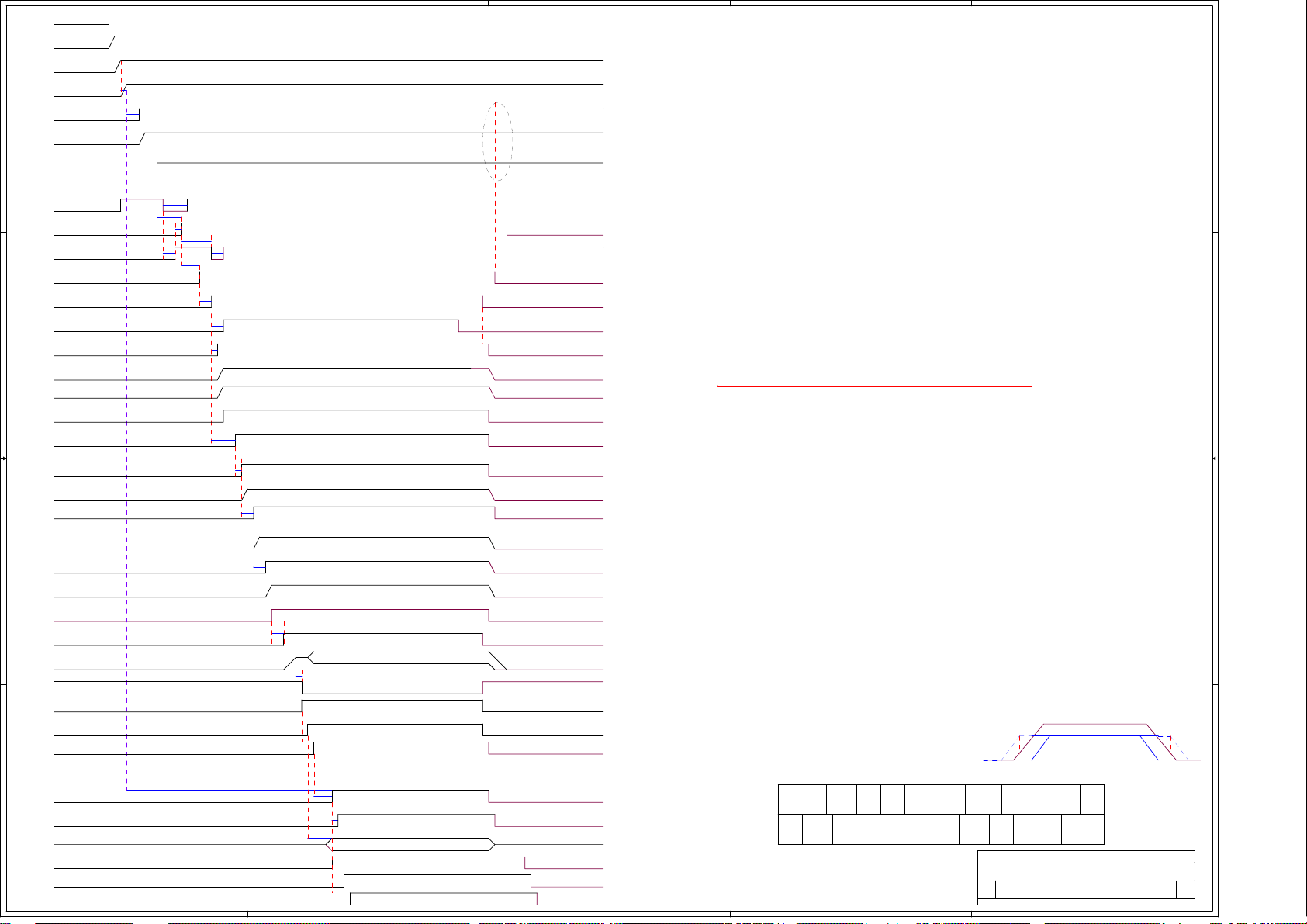
MS90 Power On Sequence Timing
Version : 0.5
+ECVCC
ECRST#
D D
ALW_ON
+5VALW/ +3VALW
ALW_PWRGD
(Waiting for Power ON)
PWRSW#
PM_RSMRST#
PWRBTN#
SLP_S5#
SLP_S4#
SLP_S3#
C C
SUS_ON (From EC- SLPS4#)
+3VSUS/ +5VSUS
+1_8VSUS/+0_9VSUS/+1_25VSUS/+1_05VSUS
DDR2_PWRGD
SUS_PWRGD_10MS
RUN_ON
+3VRUN/ +5VRUN/+1_5VRUN
+2_5VRUN/+1_25VRUN/+1_05VRUN
PEX_VDD/NVVDD
B B
RUN_ON2
T00
T01
(EC output)
(V5REV_SUS power up befor VccSus3_3, power down
after VccSus3_3. Otherwise tolerance 0.7mv)
(From MAX8734 (+3VALW & +5VALW) PGOOD to EC)
(EC initial PWRBTN# by PWRSW# keep low over 15ms)
T03
T02
T13
(5ms)
T05
T14
T12
(150ms)
T04
(50ms)(700ms)
(From EC to ICH8)
(From EC to ICH8)
(From ICH8 to EC)
T06
T08
(From ICH8 to EC)
T06
(From ICH8 to EC)
EC : SUS_ON goes to Hi after SLP_4# keep Hi 1ms
(0V to 1.8V -> Max. 2ms for DDR2)
(From SC486 PGD to EC, but EC no reference this signal now)
T07
T08
(EC : 1ms)
T09
(EC : 5ms)RUN_ON1
ALW_Power ON when AC in or Batt in only
NOTE :
1.
T00 : R=47K , C = 0.1uF is ENE recommand value please refer to KB3910B0-AN4A-200
2.
T01 : 5ms is for ALW VCC supplies must never be active while the ECVCC supply is
inactive.(Please refer to Intel 19513 Page 286 of t200 timing) --> Check(t200 did not say so)
PS : For KB3910 timing : After ECRST# goes to high ,EC must be check sum and initialized
register.For MS01, we measure the T01 Min. 200ms is needed.In MS10 , we will measure this
timing again.
3.
T02 : ALW_PWRGD:H to PM_RSMRST#:H at least 10ms (Refer t204 of Intel 20271 page 304)
4.
T04 : For MS01 SPEC Min. is 50 ms(Normal SPEC is 20ms)
5.
T05 : RSMRST# active High to SLP_S5# active High Max. is 110ms (Refer to t231 of Intel 20271 page 306)
6.
T06 : Please reference t233/t234 of Intel 20271 page 306 => Checking
7.
T07 : For MS01 current SPEC Min. is 25 ms.--> Checking
8.
T08 : For MS01 current SPEC Min. is 1 ms(1ms is EC KB3910 at least response time)
9.
T09 : EC delay 5ms
10.
T10 : Please refer to t214 of Intel 20271 page 304
11.
T11 : Please refer to t215 of Intel 20217 page 304
12.
T12 : PM_RSMRST# ACTIVE HIGH TO PM_PWRBTN# ACTIVE LOW is 150ms(Normal SPEC is
110ms;Please reference Intel 16971 Page 301of t232 timing) -->Checking
13.
T13 : For MS01 current SPEC Min. is 700 ms(Normal SPEC is 1ms that EC can response)
14.
T14 : For MS01 current SPEC Min. is 5 ms
15.
When Powered on, the DDR2 1.8V rail must ramp up from 0 to 1.8V within 2ms. (Refer to Intel 20517 page 441)
16.
IMVP_OK is same with SB_PWRGD(reserved And Gate with SYS_PWRGD)
17.
In NV4X power sequence : NV_VDD,VRAMVDD,PEX_VDD and VRAM_TERM can ramping up anytime after +3VRUN
starts ramping up.(Please refer to DG-00969_v05c Page 50 for NV4x GPU power sequencing description)
18.
T15 : Refer ISL6262A Spec no mention.
19.
T16 : Refer ISL6262A Spec page3 PGOOD DELAY.
20.
T17 : Refer to ICS9LPR501YGLFT CK505 Spec.
21.
T18 : The ICH8 drives PLTRST# inactive a mininum of 1ms after both PWROK and VRMPWRGD
are driven high. (Refer to Intel 20217)
22.
CPUPWRGD is an output signal that represents a logical AND of the ICH8's PWROK and VRMPWRGD signals.
23.
T20 : From ECRST# L->H to IMVP_PWRGD L->H. If EC's 32KHz is not stable, LPC I/F will
hang. So the 1sec must be guaranteed.(Requested by Doi's san 05/13)
( EC KB3910 Min. response time is 1ms)
(For external VGA chip)
(EC : 5ms)
+1_8VRUN
RUN_PWRGD
IMVP_VR_ON
VHCORE
VRMPWRGD
CLK_PWRGD
IMVP_OK
A A
IMVP_PWRGD
T20
STPCLK#
BCLK, SRCCLK, PCICLK
CPU_PWRGD
PLT_RST#/
H_CPURST#
(From ICH8 to CPU)
(From ICH8 to GMCH)
(From GMCH to CPU)
5
(From MAX8743(1_05V & 1_5V) PGOOD to EC)
T10
(From EC to IMVP_VR's SHUT#)
T15
(From IMVP6_CLKEN# )EC_CLK_EN#
(EC_CLK_EN# inverse to ICH8 VRMPWRGD )
(From ICH8M to CK505's CK_PWRGD)
T16
T17
(From IMVP6_PWRGD to EC)
(From EC to NB's PWROK & SB's PWROK)
T19
T11
Running
T18
4
Remark:
3
(Item1,2,3 add Diode; Item4,5,6 add dischage circuit; Item7 for implement TV)
SPEC please refer to Intel 20517 16.7 GMCH/ICH8M Platform Power -up
Requirements)
1. V5REF(+5VRUN) -> +3VRUN, dt:0.7mV
2. V5REF_SUS(+5VALW) -> +3VALW, dt:0.7mV
3. +2.5VRUN -> GMCH_VCC(1.05V), dt:0.7mV
4. +1_5VRUN -> +1_05VRUN, dt:0.7mV
5. +3.3VRUN -> +2_5VRUN, dt:0.3mV
6. +3.3VRUN -> +5VRUN (VccLAN), dt:0.3mV
7. +3_3VRUN -> +1_5VRUN(TV), dt:0.7mV
8. Check +1_05VRUN and VCC1_5_A[25] => Refer Intel 20517 page 438
T00
R/C delay
(47K/
0.1uF)
Max.
50ns
T12
Min.
150ms
T01
Min.
5 ms
T13T11
Min
700ms
T02
Min.
10 ms
2
T04T03
Min.
Min.
40ms
50ms
T14 T18T16
T15
Min : 5.5ms
Min
TBD
Max : 8.1ms
5ms
T05
Max.
110ms
Max
1.8ms
dv
T06
T07 T10
1 - 2
RTCCLK
Min.
(Checking)
25 ms
T17
Min
1ms
Title
Title
Title
<Title>
<Title>
<Title>
Size Document Number Rev
Size Document Number Rev
Size Document Number Rev
<Doc> <RevCode>
C
<Doc> <RevCode>
C
<Doc> <RevCode>
C
Date: Sheet
Date: Sheet
Date: Sheet
T08
1ms
T19
Min : 99ms
High Voltage
Low Voltage
T09
Min.
Min.
99ms
5ms
T20
Min :1s
1
dv
of
11Tuesday, February 27, 2007
of
11Tuesday, February 27, 2007
of
11Tuesday, February 27, 2007
Page 4
5
4
3
2
1
D D
Change List
[V0.2]
1. STPCLK#, CPUSLP#, STP_CPU#/PCI# --> STPCLK#
2. Correct T11 from "IMVP_OK to STPCLK#" --> "IMVP_PWRGD to STPCLK#" (Refer ICH8M EDS T215)
3. Correct down side table T09 from 10ms to 5ms.
4. Correct T18 from "IMVP_OK to PLT_RST#" --> "IMVP_PWRGD to PLT_RST#" (Refer ICH8M ESD)
5. Correct H_CPURST to H_CPURST#
6. Add ICH8M's CK_PWRGD to enable CK505's PWRGD
7. Update CLK_EN# to EC_CLK_EN#
C C
[V0.3]
1. Correct: PWRSW# is driven by EC, not ICH8M
2. Add note: Check if it's ok to use IMVP_OK to replace EC_CLK_EN#, it can save one inverter
[V0.4]
1. Add power off sequence
[V0.5]
1. Correct T12 from min:400ms to 150ms
This modify already phase in MS90-DVT stage.
B B
A A
Title
Title
Title
Size Document Number Rev
Size Document Number Rev
Size Document Number Rev
Date: Sheet of
Date: Sheet of
5
4
3
Date: Sheet
<Title>
<Title>
<Title>
<Doc> <RevCode>
A
<Doc> <RevCode>
A
<Doc> <RevCode>
A
of
11Tuesday, February 27, 2007
11Tuesday, February 27, 2007
2
11Tuesday, February 27, 2007
1
 Loading...