

Page 1
KY-27EXR95
/
,SERVlCEMANUAL
RM-Ylll
*
US Model
Chassis No. SCC-DSOK-A
Canadian Model
Chassis No. SCC-Q61 E-A
ANU-2
MODELS OF THE SAME SERIES
KV-27EXR95
KV-27EXR90
CHASSIS
Television system American TV standards
Channel coverage VHF: 2 - 13
Picture tube
Antenna
Input
output
UHF: 14 - 69
Cable TV: 1 - 125
MicroblackL’ Trinitronr
27.inch
picture measured
diagonally
28-inch
picture tube measured
diagonally
75.ohm external anlenna terminal
for VHF/UHF
VIDEO 1 and 2 IN
S VIDEO IN
Y: 1 Vp-p,
C: 0.286 Vp-p (Burst signal),
Video (phono jacks): 1 Vp-p,
75-ohms unbalanced,
sync negative
Audio (phono jacks): 500
(100% modulation)
Impedance: 47 kilohms
VIDEO 2 OUT
Video (phono jack):
75-ohms unbalanced,
sync negative
Audio (phono jacks):
Impedance: 10 kilohms
AUDIO OUT (VARIABLE)
(phono jacks)
More than 408
maximum volume setting
(variable)
Impedance: 5 kilohms
(4-pin
mini
75-ohms
unbalanced, sync negative
75ohms
mVrms
tube
at the
DIN)
mVrms
SPECIFICATIONS
Speaker output
Power requirements 120 V AC, 60 Hz
Power consumption Maximum: 165 W
Dimensions (h/w/d) 595 x 683 x 573.5 mm
Supplied accessories
Recommended accessories
SPEAKER SIZE TWEETER 50mm X2
INTERNAL
CONDITION
AUDIO FREQUENCY RESPONSE
CONDITION
Design and specifications are subject to change without
notice.
5Wx2
Standby: 1.5 W
(23% x 27 x 22% inch)
Remote Commander RM-Ylll (1) with
2 size AA (R6) EVEREADY batteries
Terminal cover (1)
U/V mixer EAC-66
Connecting cable
VMC-8101820.S
WOOFER 85mm X2
AUDIO POWER
FRONT 5 WATTS X 2
8 ohms, 10%
TWEETER 2kHz
WOOFER
BASS/TREBLE ARE IN NORMAL CONDITION
YCi5V13OV
(2”)
(3 318”)
TOTAL 2 SPEAKER BOXES
T.H.D
-2OkHz
50Hz
-2kHz
TRINITRONdOLOR
s;ONYn
TV
Page 2
TABLE OF CONTENTS
Section
Title
m
1. GENERAL
l-l.
Location of Controls
1-2.
Presetting TV Channels ....................
Waching
1-3.
1-4.
Adjusting Picture and Sound Quality
1-5.
Using Picture-in-Picture.
1-6.
Using the Remote Commander ...............
TV Programs ......................
1-7. Using the guide Function
1.8.
Enjoying Other Useful Features .............
1-9. Troubleshooting
......................
.........
.....................
.....................
.........................
4
5
6
7
9
11
13
19
20
2. DISASSEMBLY
2-1.
Rear Cover Removal
2-2.
Ul and U2 Boards Removal ...................
2-3. Service Position
2-4.
Picture Tube Removal ......................
..........................
..........................
21
21
21
22
3. SET-UP ADJUSTMENTS
Beam Landing ................................
3-1.
3-2. Convergence
Focus
3-3.
................................
....................................
3-4. G2 (Screen) and White Balance Adjustments
....
23
24
26
26
Section Title
4. SAFETY RELATED ADJUSTMENTS . . . . . . . . . .
&
28
5. CIRCUIT ADJUSTMENTS
5-l. Electrical Adjustment by Remote Commander . .
5-2.
A Board Adjustments . . . . . . . . . . . . . . . . . . . . . . .
5-3.
P Board Adjustments .
. . . . . . . . . . . . . . . . 37
31
33
6. DIAGRAMS
BlockDiagram.......
6-1.
Circuit Boards Location . . . . . . . . . . . . . . . . . . . .
6-2.
6-3.
Printed Wiring Boards and
Schematic Diagrams
6-4. Semiconductors
. .
. . . . . . . . . . . . . . . . 39
. . . . . . . . . . .
. . . . . . . .
. . . . . . . . . . . . . . . . . . . . . .
43
43
67
7. EXPLODED VIEWS
Chassis . . . . . . . . . . . . . . . . . . . . . . . . . . . . .
7-1.
Picture Tube......... . . . . . . . . . . . . . . . . . . . .
7-2.
8. ELECTRICAL PARTS LIST . . . . . . . . . . . . . . .
69
70
71
WARNING !! ATTENTION!!
AN ISOLATION TRANSFORMER SHOULD BE USED
DURING ANY SERVICE TO AVOID POSSIBLE SHOCK
HAZARD, BECAUSE OF LIVE CHASSIS.
THE CHASSIS OF THIS RECEIVER IS DIRECTLY CONNECTED TO THE AC POWER LINE.
SAFETY-RELATED COMPONENT WARNING !!
COMPONENTS IDENTIFIED BY SHADING AND MARK
! ON THE SCHEMATIC DIAGRAMS, EXPLODED
n
VIEWS AND IN THE PARTS LIST ARE CRITICAL TO
SAFE OPERATION. REPLACE THESE COMPONENTS
WITH SONY PARTS WHOSE PART NUMBERS APPEAR
AS SHOWN IN THIS MANUAL OR IN SUPPLEMENTS
PUBLISHED BY SONY. CIRCUIT ADJUSTMENTS
THAT ARE CRITICAL TO SAFE OPERATION ARE
IDENTIFIED IN THIS MANUAL. FOLLOW THESE PRO-
CEDURES WHENEVER CRITICAL COMPONENTS ARE
REPLACED OR IMPROPER OPERATION IS SUSPECTED.
-2-
AFIN D’EVITER TOUT RISQUE D’ELECTROCUTION
PROVENANT D’UN CH/iSSlS SOUS TENSION, UN
TRANSFORMATEUR D’ISOLEMENT DOIT ETRE
UTlLlSi
LE
RACCORDi ii L’ALIMENTATION SECTEUR.
LES COMPOSANTS IDENTIFIES PAR UNE TRAME ET
PAR UNE MARQUE
LES VUES EXPLOSiES ET LES LISTES DE PIECES
SONT D’UNE IMPORTANCE CRITIQUE POUR LA
SiCURlTi
PLACER QUE PAR DES COMPOSANTS SONY DONT LE
NUMiRO DE
MANUEL OU DANS DES SUPPLEMENTS
SONY. LES RiGLAGES DE CIRCUIT DONT L’IMPOR-
TANCE EST CRITIQUE POUR LA SiCURITk DU
PRiSENT MANUEL. SUIVRE CES PROhDURES LORS
DE CHAQUE REMPLACEMENT DE COMPOSANTS
CRITIQUES, OU LORSQU’UN
MENT EST SUSPECTi.
LORS DE TOUT
CHkSlS
ATTENTION AUX COMPOSANTS RELATIFS A LA
FONCTIONNEMENT SONT IDENTIFIES DANS LE
DE CE RECEPTEUR EST DIRECTEMENT
DU FONCTIONNEMENT. NE LES REM-
PIlkE
DiPANNAGE.
SkURITt?!!
ASUR
LES
SCHiMAS
EST INDlQUi. DANS LE
MAUVAIS
DE PRINCIPE,
PRkENT
PUBLIh
FONCTIONNE-
PAR
Page 3
SAFETY CHECK-OUT
(US Model only)
After correcting the original service problem,
perform the following safety checks before releasing
the set to the customer:
1.
Check the area of your repair for unsoldered or
poorly-soldered connections. Check the entire
board surface for solder splashes and bridges.
Check the interboard wiring to ensure that no
2.
wires are “pinched” or contact high-wattage
resistors,
3. Check that all control knobs, shields, covers,
ground straps, and mounting hardware have
been replaced. Be absolutely certain that you
have replaced all the insulators.
4. Look for unauthorized replacement parts, par-
ticularly transistors, that were installed during a
previous repair. Point them out to the customer
and recommend their replacement.
5. Look for parts which, though functioning, show
obvious signs of deterioration. Point them out
to the customer and recommend their replacement.
6.
Check the line cord for cracks and abrasion.
Recommend the replacement of any such line
cord to the customer.
7.
Check the condition of the monopole antenna
(if any).
Make sure the end is not broken off, and has
the plastic cap on it. Point out the danger of
impalement on a broken antenna to the
customer,
replacement.
8.
Check the B+ and HV to see they are at the
values specified. Make sure your instruments
are accurate; be suspicious of your HV meter
if sets always have low HV.
9.
Check the antenna terminals, metal trim,
“metallized” knobs, screws, and all other
exposed metal parts for AC leakage.
leakage as described below.
and recommend the antenna’s
Check
LEAKAGE TEST ’
The AC leakage from any exposed metal part to
earth ground and from all exposed metal parts to any
exposed metal part having a return to chassis, must
not exceed 0.5 mA (500 microampers).
Leakage
current can be measured by any one of three
methods.
A commercial leakage tester, such as the
1.
Simpson 229 or RCA WT-540A. Follow the
manufacturers’ instructions to use these instruments.
2. A battery-operated AC milliammeter. The Data
Precision 245 digital multimeter is suitable for
this job.
Measuring the voltage drop across a resistor by
3.
means of a VOM or battery-operated AC volt-
meter. The “limit” indication is 0.75 V, so
analog meters must have an accurate
voltage scale.
The Simpson 250 and Sanwa
low-
SH-63Trd are examples of a passive VOM that
is suitable. Nearly all battery operated digital
multimeters that have a 2V AC range are
suitable. (See Fig. A)
HOW TO FIND A GOOD EARTH GROUND
A cold-water pipe is guaranteed earth ground; the
cover-plate retaining screw on most AC outlet boxes is
also at earth ground. If the retaining screw is to be
used as your earth-ground, verify that it is at ground
by measuring the resistance between it and a
cold-
water pipe with an ohmmeter. The reading should be
zero ohms.
If a cold-water pipe is not accessible,
connect a 60-100 watts trouble light (not a neon
lamp) between the hot side of the
receptacke
and the
retaining screw. Try both slots, if necessary, to locate
the hot side of the line, the lamp should light at
normal brilliance if the screw is at ground potential.
(See Fig. B)
‘ig.
To Exposed Metal
Parts on Set
AC
voltmeter
(0.75 V)
*
Earth Ground
A.
Using an AC voltmeter to check AC leakage.
-3-
Trouble Light
1
AC Outlet
I
Fig. B. Checking for earth ground.
Box
Ohmmeter
Cold-water Pipe
Page 4
l-l.
GUIDE Functton displays
Picture-Sound level
adjustment displays
(0)
CURRENT TIME displays
LOCATION OF CONTROLS
SRS display
1
--~~~~
-l-r
TvNlDEO - YOL”ME +-
~-yzrz-----
I
I r ____ ------- ____
, -----
,:
L--------------J
____
-__-_
----e!---me.1
7
CL + mm STEFZEO
--
CH*,NNI
3
b
Picture-m-Picture mput mode
Bar display for volume.
I
or sound adjustment
I 1
i
POWER
SECTION 1
GENERAL
paws
VIDEO 1 IN jacks (S VIDEO,
VIDEO/AUDIO)
VHFIUHF
antenna terminal
SPEAKER termmals
AUDIO OUT
(VARIABLE)
tacks
VIDEO 2 IN and OUT jacks
1
Stortnq the AC dower cord
You can
store
the termmal cover, as illustrated here.
I
the AC power cord at the rear of
1
TVNIC
JEO
T
T
CHI 4Nh
VOLUME +/- buttons’
button*
’ ‘j”
STEREO mdlcator tamp
TIMER mdlcator lamp
IEL
+/-
buttons’
POWER button*
Remote control detector
Altachmg the termmal cover
The termmal cover comes packed separately from the TV.
to use w,th your TV, then attach the cover as shown below.
Insert
the two tabs at the top of the termmal cover
mto
the rear panel as shown below. cords extend out from the
1
To remove the termmat cover
Pull the cover away from the rear panel to the angle shown m step 1. then pull down to release the cover
from the rear panel.
Ftrst
connect any opbonal equipment you want
Push the cover onto the rear panel so that the connected
12
I
Ill+==%
I,, I
openmg
at the bottom.
I,, /
I/
Page 5
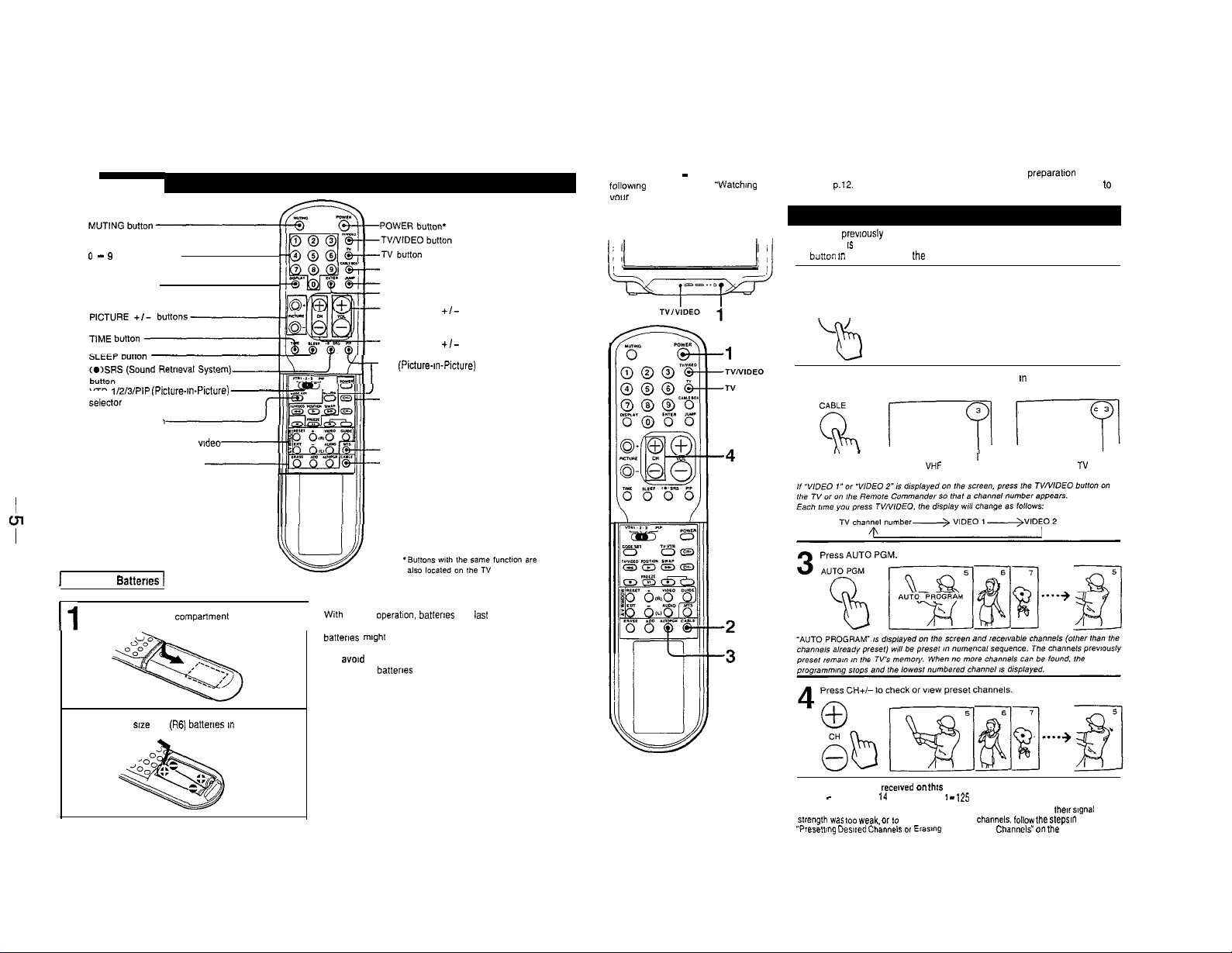
0 - 9
number buttons
DISPLAY button
CABLE BOX button
JUMP button
ENTER button
VOL (volume)
+/-
buttons*
1-2. PRESETTING TV CHANNELS
VHF channels (2 - 13) have been preset on your TV. You can watch those TV channels without further preparatton by
followmg the steps under “Watchmg TV Programs” on p.12. For UHF and cable channels. you must first preset channels to
“our
TV
If you have prewously pressed the CABLE BOX button, the Remote
Commander IS set to control the cable converter box. not the TV. Press the
TV biltton m order to control the TV with the Remote Commander.
Press POWER on the TV or the Remote Commander to turn the TV on
1
POWER
n
VTR 1/2/3/PlP lPicture-In-Picture)
Selector
CODE SET button
(Pre-Programmed function)
A/V WINDOW (audio and wdeo
adjusting) buttons
Channel presetting buttons
1
Installing Batteries
Remove the battery Compartment cover.
I1
Insert two sne AA
2
1
(R6)
battertes m correct polarity.
CH (channel)
PIP (Picture-In-Picture) buttons
+/-
buttons’
J
Video operating buttons
MTS (multichannel TV sound) button
CABLE button
Battery life
With normal operation. batlerles will
’
If the Remote Commander does not operate properly, the
I
batferles mlghl be exhausted. Replace both with new ones.
~ To avold damage from possible battery leakage
Remove the batteries when the Remote Commander will
not be used for a long time.
last
up to hall a year.
Press CABLE so that a channel number appears m the mode that
you want to preset. TV or cable.
2
To preset VHF or UHF channels To preset cable TV channels
Channels that can be
VHF. 2 - 13
To add channels that could not be preset automatically because
strengm was too
“Presenlng DeSlled Channels or Erasing
recewed
UHF 14 -69
weak. or 10 erase unnecessary
on thts TV:
Cable: 1 -
I
125
channels. follow me steps In
unnecessary
Channels” on ule
I
their slgnal
next page.
Page 6
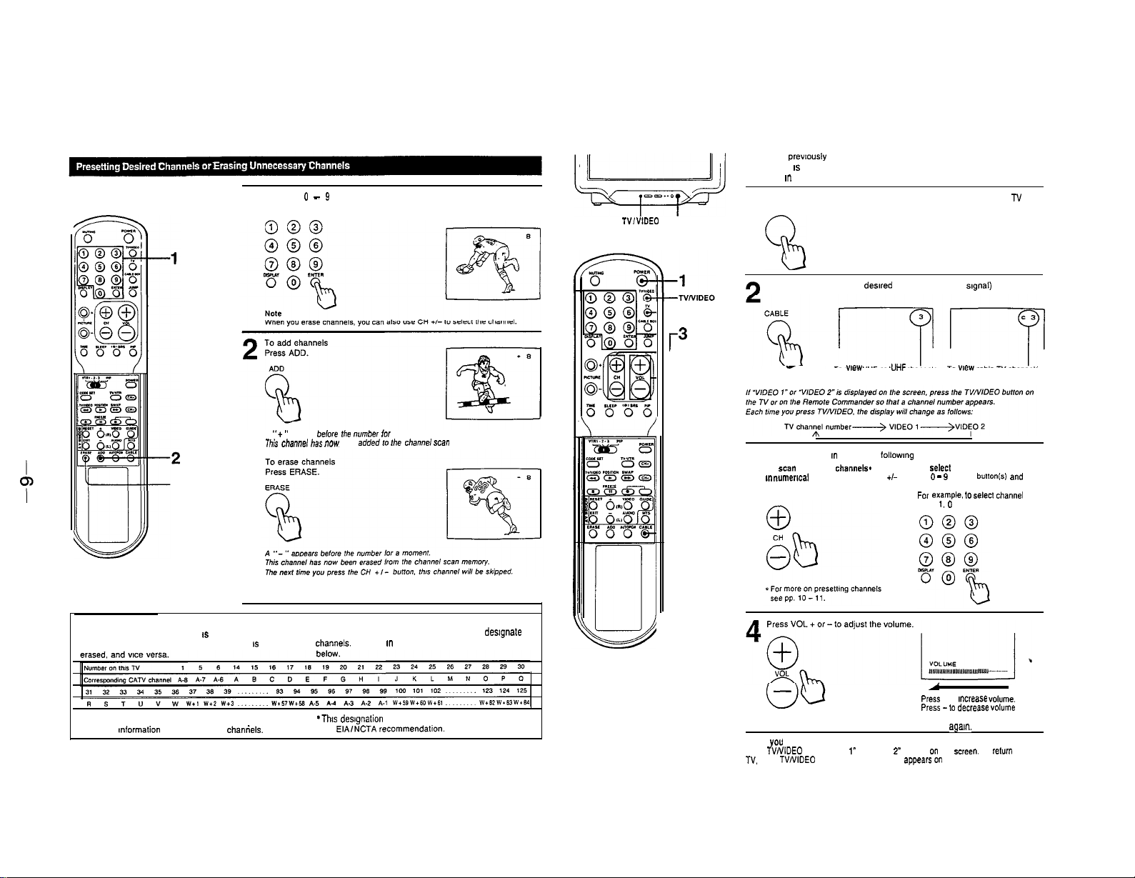
Press the 0 - 9 “umber button(s) and the” press ENTER to select the
channel you want to add or erase.
1
1-3. WATCHING TV PROGRAMS
If you have prewously pressed the CABLE BOX button. the Remote
Commander IS set to control the cable converter box, not the TV. Press the
TV button m order to control the TV with the Remote Commander.
kyfiFfg
TV,WDEO
1
-TV
Press POWER on the TV or the Remote Commander to turn the N on.
POWER
1
3
Press CABLE so that the dewed mode (au or cable
r3
-4
signal)
appears
To wew VHF or UHF channels To wew cable TV channels
A “+ ” appears belore
This
ERASE
Repeat steps 1 and 2 to add or erase other channels.
CAUTION
When a VHF or UHF channel IS erased
The cable TV channel with the same number IS also
Check with your local cable TV company for more
complete mformation on the available chanriels.
*Ire
“umber
ior
Ctm”“d /la*
“OW
bee” added ,o me channel scan memory.
Cable TV channel chart’
Cable TV systems use letters or numbers to deslgnate
charm&. To tune I” a channel. refer to the chart
*Thts designation of cable TV channels conforms to
the ElAlNCTA recommendatom
a moment.
-2
Select a channel m one of the followmg two ways:
To
scan
3
TO turn off the TV
Press POWER on the TV or the Remote Commander
When you want to watch the connected VCR
Press TVNlDEO until “VIDEO 1” or ‘VIDEO 2” appears on the screen. To return to the
TV. press TVNIDEO until the channel number appears on the screen.
the preset channels*
I”
““merlcat sequence. press CH +,-I;
I
To *elect a channel directly. press
the 0 - 9 number button(r) and the”
ENTER.
For
example. 10 Select channel to.
press 1. 0 and ENTER.
/
Press
press
+ to
-to
agam.
.
Increase volume.
decrease volume
Page 7
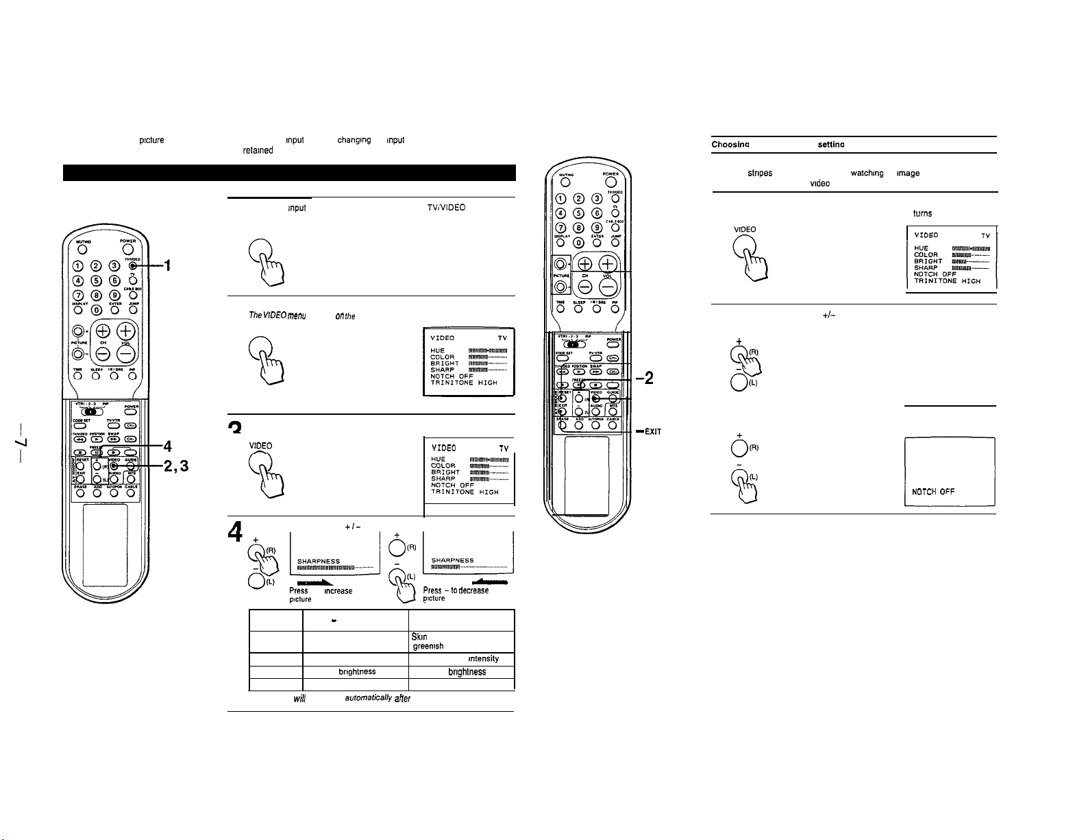
14. ADJUSTING PICTURE AND SOUND LEVELS
You can set different pxture and sound quality levels for each Input mode by changing the Input mode
(TVNIDEO) before setting. These settings will be retalned even when you turn the TV off.
Select the Input mode you want to adjust with the TV/VIDEO button
1
TVNIDEO
Press VIDEO.
me
WDEO menu
appear* on
rhe
2
VIDEO
9
Press VIDEO repeatedly until the item you want to adjust turns red
3
VtDEO
-
Press the AIV WINDOW
screen.
+I-
buttons to make the adjustment.
“IDE0
TY
-PICTURE
+ I-
- RESET
-2
-1
-
EXIT
Choosinq the NOTCH filter settina
Under normal conditions, set NOTCH OFF
If dots or
Stripes
computer game software or wdeo source, set to NOTCH ON.
1
2
appear while you are watchmg an
Press VIDEO.
Press VIDEO repeatedly until the NOTCH setting turns red
Press the AN WINDOW +/- buttons to select ON or OFF
Press + to select ON.
Image
from a computer,
+
m
%
O(L)
Press-to select OFF
NOTCH
El
OFF
Picture
quality
HUE
COLOR
BRIGHT
SHARP
The display
Press
+ to
InCreaSe
p,ct”re sharpness
Press - (L) button
1 Skin tones become
purplish
For less color Intensity
For less
brightness
For less sharpness
wi//
disappear aofomatically
Press
-to
picture sharpness
Press + (R) button
1 Skm tones become
greemsh
For more color mtensity
For more
brightness
For more sharpness
aHer
a few seconds.
decrease
Page 8
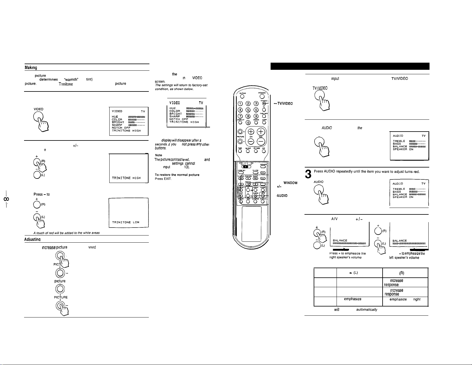
Makmg
the TRINITONE adjustment
Color
pncture
(tint) that deiermmes the %armth” (red bnt) or “coolness” (blue tine) of the
picture. With Sony’s Trmitone feature, you can adjust the
preference.
1
tubes are usually manufactured with a fixed color temperature
picture
color to your
Press VIDEO.
Press VIDEO repeatedly until the TRINITONE setting turns red.
To restore the factory settings
Press RESET while I” the VtDEO menu
SCrW”.
VIDEO TV
Select the Input mode you want to adjust with the TVNIDEO button.
1
TVlVtDEO
Press the AN WINDOW +/- buttons to select HIGH or LOW.
Press + to select HIGH.
2
The factory preset whiteness will be restored
Press-to select LOW.
Adiustinq
the Picture Contrast
Press + to mcrease
Press-to decrease
p!cture
contrast with
+
0
P,Cj
b
o-
pocture
contrast with soft color.
+
0
P,Ci”RE
vwd
color.
TRINITDNE HIGH
I I
The
dis@ay will drsappear
seco”ds, rf you
b”,,O”S.
The
wure
Contras,
TRINITONE seltrngs cannot be stored under
each
cnput
mode (p.
af,er a few
do “otp,ess
IWd. NOTCH
13).
any olhe,
and
--RESET
-AN
+I-
WNDOW
Press AUDIO.
The AUDlO menu appears on the screen
2
AUDIO
T--l
Press the A/V WINDOW
4
.L
’
Sound
quality
TREBLE
BASS
BALANCE
The displays
Press To decrease treble
response
To decrease bass TO
response
To emphasize the left
speaker’s volume
will
disappear automalicafly after a few seconds.
+/-
buttons to make the adjustment.
Press -to
left speaker’s volume
(L)
button Press +
To ,“crease treble
VS?+OllS~
Increase
ESpO”Sf!
To emphasize the
speaker’s volume
emphasue the
(R)
button ,
bass
right
Page 9
cb
I
I
Turnmg SPEAKER ON/OFF
Press AUDIO.
Press AUDIO repeatedly until the SPEAKER setting turns red.
1
L
Press the AN WINDOW +/- buttons to select ON or OFF
Press + to turn on the speakers connected to theSPEAKER termmals.
2
.&
SPEAKER ON
Press-to turn the above speakers off, in order to use an audio system
connected to the AUDIO OUT (VARIABLE) lacks.
Selecting AUDIO-OUT FIX mode.
Press AUDIO.
Make sure that the SPEAKER OFF setting IS selected (see above).
1
Press AUDIO repeatedly until the AUDIO-OUT setting turns red.
AUDIO
l---J
AUDIO-OUT “AR mode. and VOLUME.
TREBLE. BASS and BALANCE settings prior
10
AVOIO-OUT FIX settings are restored.
To restore the factory settings
Press RESET while m the AUDIO
mew
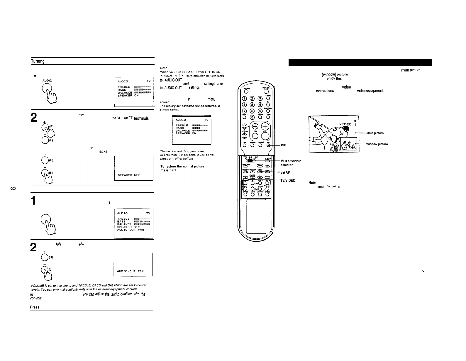
1-5. USING PICTURE-IN-PICTURE
’lo
--SWAP
-NNIDEO
With the Picture-In-Picture function, you can watch both the man
second (wndow) picture at the same time.
In order to
enjoy
video disc player, etc.) to the TV. Then you can watch two TV programs, or
a TV program and a wdeo source at the same time.
For instructions on connecting wdeo equtpment.
Note
If the
Press EXIT to cancel CHANNEL BLOCK. (Setting CHANNEL BLOCK.)
the. function, first connect your video equipment (VCR,
man
p~ture 15 blocked. Picture-In-Picture does not function.
picture
and a
Press the A/V WINDOW +/- buttons to select FIX or VAR.
Press-to select FIX.
2
I” AUDIO-OUT “AR (VARIABLE, mode, you can ad,“s, Ihe audro quahfies
con,,o,s.
To change to AUDIO-OUT VAR mode
Press
+.
wlh
Ihe TV
Page 10
I.
To display 8 window picture - PIP
To change the input mode of a wmdow picture
TvMLeO
Press m on the Remote Commander. Each time you press
TV, VIDEO 1 or VIDEO 2 mode will be selected in sequence.
Picture-m-Picture also functions when the mam picture IS m VIDEO mode.
To swap the main and wmdow pictures -SWAP
I
.
Set the VCR
Press PIP to
i/2/3/PIP
display
a wmdow
selector to PIP
VTR 1 -2 -3
picture.
PIP
thts
button,
2
To make the rnndow picture disappear
press
PIP
.?+a,“.
TO
scm
channels in the window ptcture
Press CH +/-on the Remote Commander.
Notes on the wondow picture
l You cannot hear the sound of the wmdow
miture channel.
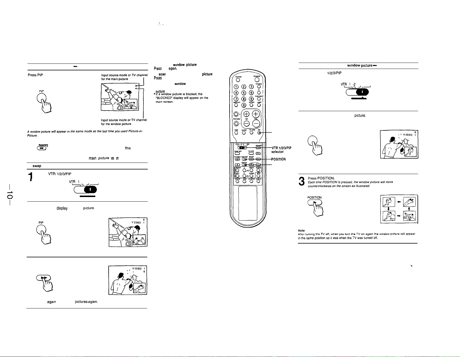
PIP
VTR
i/2/3/PIP
selector
PDStTtON
FREEZE
To change the position of the
Set the VTR
i/2/3/PIP
selector to PIP
1
VrR t -2
Press PIP to display a wmdow
2
PIP
0
b
wandow pmture -
-3
PIP
picture.
POSITION
Press SWAP
3
SWAP
Press SWAP
agam
to swap the
pictures
agal”.
Page 11
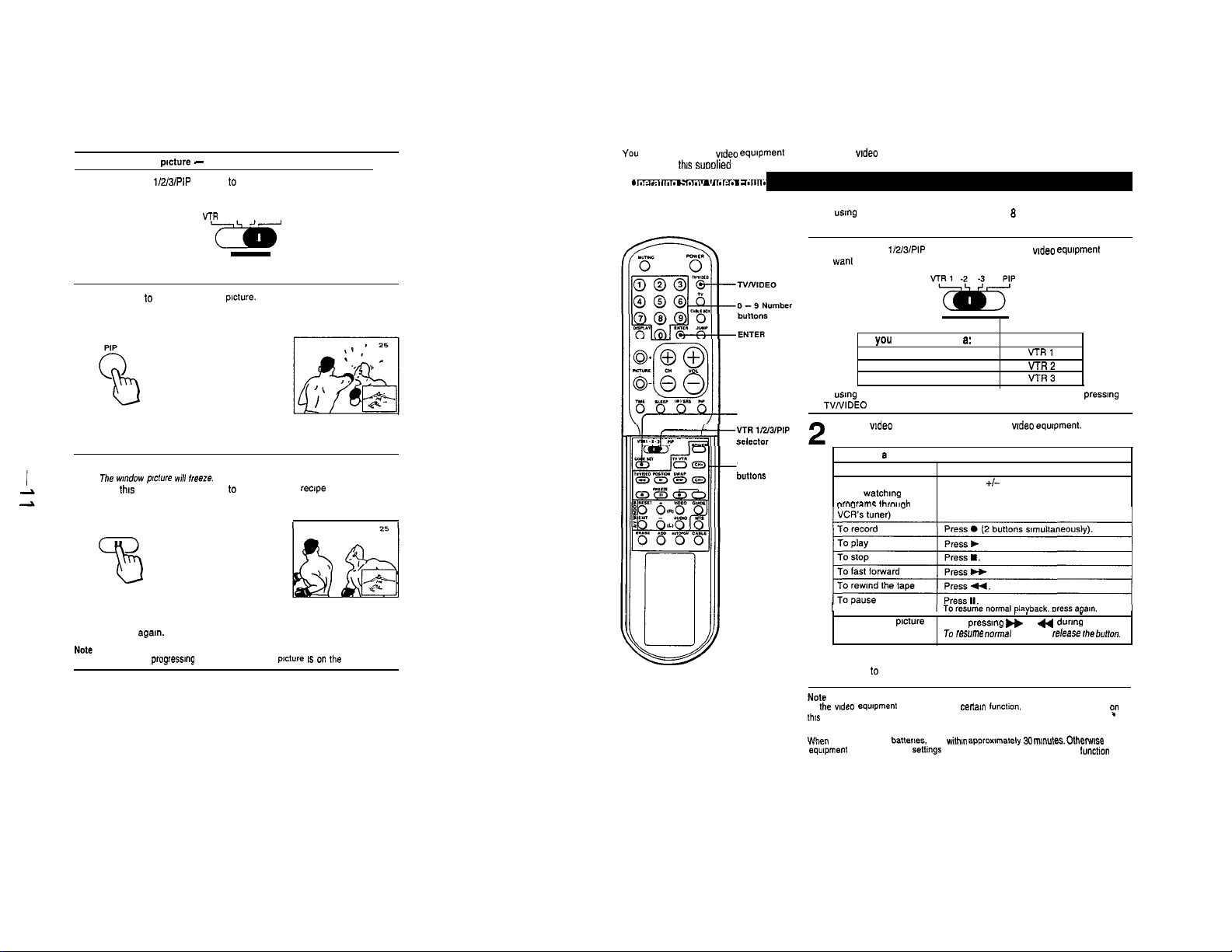
l-6. USING THE REMOTE COMMANDER
To freeze a window picture - FREEZE
Set the VTR i/2/3/PIP selector t0 PIP
1
VTR
1 -2 -3
Ye
Press PIP to display a window picture.
PIP
2
Press FREEZE.
me
W”dOW plcf”re Will freeze.
3
Use this feature when you want to write down the recipe of a cooking
program or a displayed toll free number, etc.
FREEZE
%
You can operate other wdeo equpment (such as VCRs, wdeo disc players and cable boxes) that have an Infrared remote
-
detector with
this
suoolied Remote Commander.
CODE SET
Video operating
bUttO”*
When “s!“g Sony video cassette recorders (Beta, B mm, VHS), follow the
steps below.
Set the VTR i/2/3/PIP selector according to the wdeo equipment you
want to operate.
1
If you want to operate 8:
Beta, ED Beta VCR
a mm VCR
When usmg VCR equipment. select VIDEO 1 or VIDEO 2 mode by prewng
the TVNIDEO button.
3
VHS VCR
Use the wdeo operating buttons to operate wdeo equipment.
Operating a VCR
To turn on or off 1 Press POWER.
To change channels Press CH +/-
(when watchmg TV
~roarams throwah the
Press 0 (2 buttons simultaneously).
set to:
VTRl
VTR2
VI-R3
~~
To restore the normal picture
Press FREEZE agam.
The broadcast will be progressmg normally while the still picture IS on Ihe screen
.~
To search the
forward and backwardTo
To return to TV mode
Press POWER to turn off the VCR
Note
If the “ode0
fhlS
Remote Commander will not operate.
Caution
When
you replace the batters, do it
equipment Settings and the settings you made under the Pre-Programmed lunchon
may be erased
equpment
picture
does not have a
Keep pressmg ww or a durmg playback.
resume normal
certa,”
with!” approxwnately 30
playback, rdease
lunct~on. the corresponding button
mnutes. Othewse Sony
”
Ihe bullon.
fn
Page 12
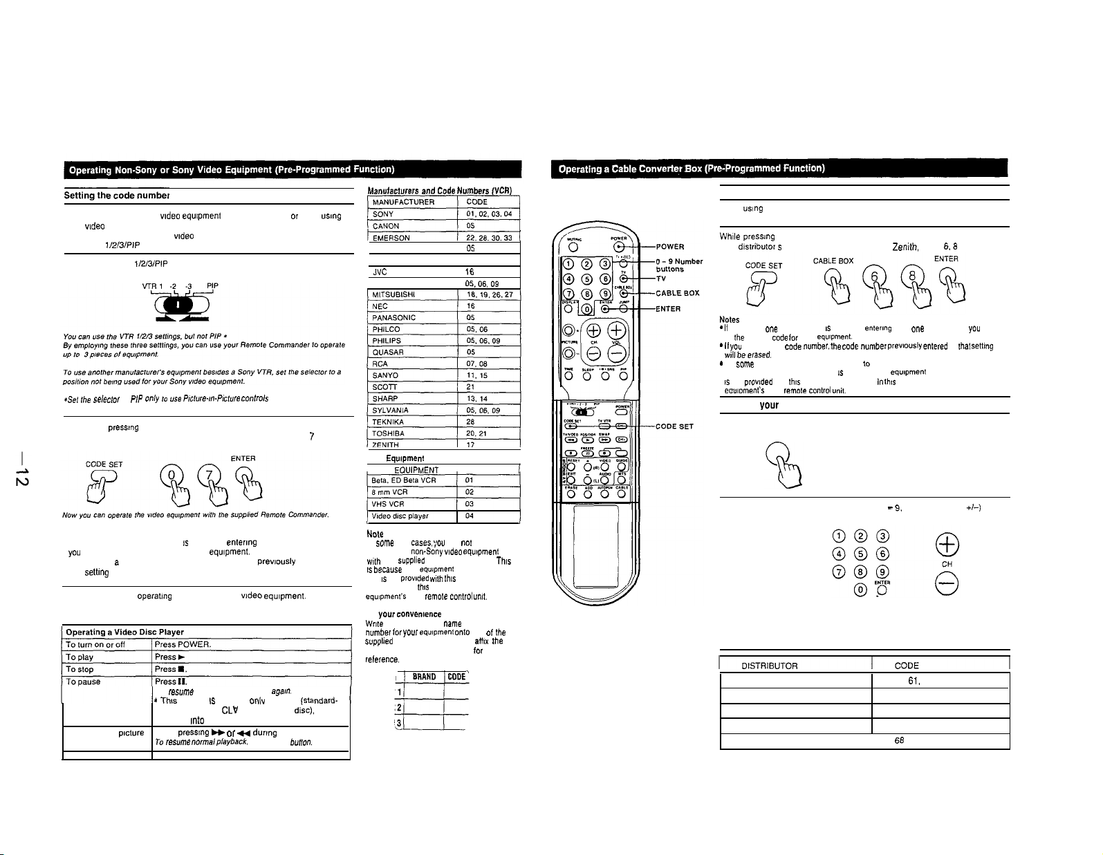
When “smg other makers’
Sony video disc player. follow the steps below.
Example: To operate an RCA wdeo cassette recorder when you set the VTR
?/2/3/PIP selector to VTR 2.
Set the VTR i/2/3/PIP selector to VTR 2.
vadeo
equipment as well as Sony’s, or when usmg a
1
*se,
Ihe *ek?c,*r to PIP only ,o use P,ct”re-m-P,ct”,e
While
pressmg
manufacturer’s code number (see charts). For RCA, press 0, 7 and
2
ENTER.
Notes
l If more than one code number
you come to the correct code for your equlpment.
. If you enter a new code number, the code number prewously entered at
that settmg will be erased.
Use the video operatmg buttons to operate wdeo equipment.
Operating a VCR
3
See the table on p. 22.
To search the
forward and backward to
CODE SET, press the number buttons for your
1s
listed, try entermg them one by one, until
To resume normal playback, press agarn.
*
Thw function IS effective onlv for CAV tstandard-
p,cture
will go mto the standby mode if II is pressed.
Keep pressing H or U durmg playback.
resume
normal playback. release the butlo”.
conlrok
di‘sc).
the TV
Ma”“,act”,e,* and Code Numbers (“CR)
-1
GENERAL ELECTRIC (
HITACHI
NC (
MAGNAVOX
Sony
Equipment
EOVIPMENT
rare
Cases, you
your
equ,pme”t
prowded
own
for your
equ,pment onto
and Code Numbers
1 SONY
NC.@
In
come
operate your non&my
wth
the suppIled Remote Commander. This
IS becauee
that IS not
Commander. I” th,s case. please use the
equrpment’s
For
your CO”“e”le”ce
Wrde the manufacturer name and code
number
suppIled self-adhesive labels and aff,x Ihe
label to the Remote Commander
WfHe”Ce.
I 07
/ 05.06.09
1 CODE
may
not
video eq”,pment
may “se a code
wth
this
Remote
remo,e control
05
16
be able to
““It.
one 0,
for
easy
the
Setting the code number
When
“song
Example: To operate a Zenith cable converter box.
Whble
your dtstributor s code number (see chart). For Zemth. press 6.8 and ENTER.
Notes
- It
* It you
*
Operating your cable converter box
1
I
2
a cable converter box. follow the steps below
pressmg CODE SET, press CABLE BOX and the number buttons for
more than
one
to
the
Will be erase*.
In some rare cases. you may not be able to operate your cable converter box with the
supplied Remote Commander. This
IS
not
eo”lome”t‘* own
code number IS listed. try
correct
coda
enter a new
prowded
Press CABLE BOX.
Use the TV control buttons [POWER, 0 - 9. ENTER and CH +I-) to
control the cable converter box.
for your equpnent.
code “umber. me code
with
thus
Remote Commander. In
remote Control
CABLE BOX
POWER
entering
them
one
by one. until
“umber
pre”lo”sly entered
IS
because your equopment may “se a code that
““it.
thts
case. please “se the
at
mat semng
you
come
0
To return to TV mode
Press TV.
You can then use the TV control buttons to control the TV.
For details, refer to the cable box’s Instructions.
JERROLD
PIONEER 69.70
SCIENTIFIC ATLANTA 66.67play disc). With CLV (extended-play
TOCOM
ZENITH
60. 61. 62, 63. 64.65
71.72
( 68
Page 13
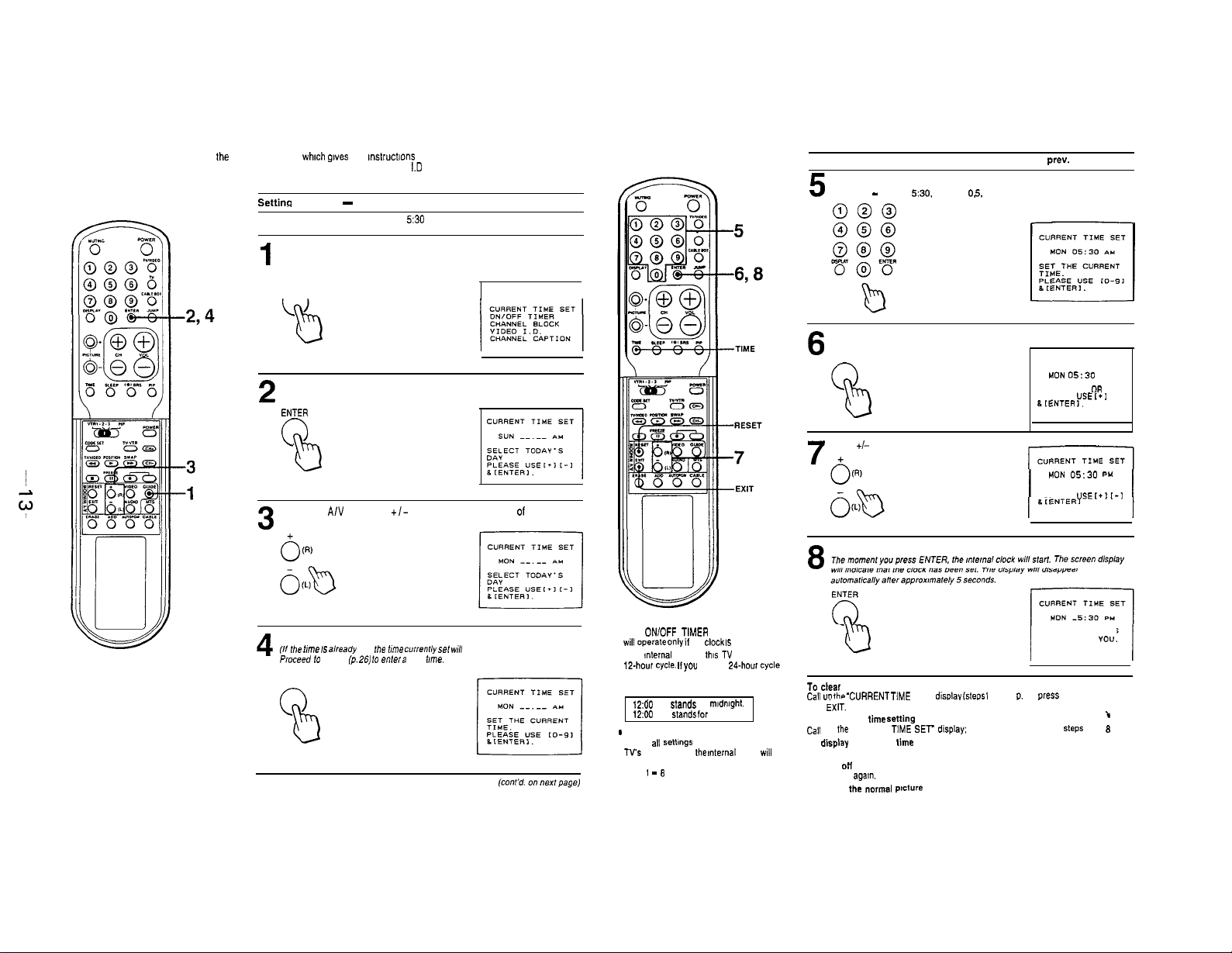
1-7. USING THE GUIDE FUNCTION
Use the GUIDE function to call up the on-screen menu, which
on how to set the CURRENT TIME, ON/OFF TIMER, CHANNEL BLOCK, VIDEO
and CHANNEL CAPTION
Settinq the Clock - CURRENT TIME SET
Example: Set the clock to Monday, 530 PM.
1
gwes
you
mstruct~ons
Press GUIDE.
Press repeatedly until the “CURRENT TIME SET” display turns red.
GUIDE
n
Press ENTER
2
ENTER
0
b
Press the A/V WINDOW
+/-
3
I.D
GUIDE
buttons to select the day of the week.
Setting the Clock -CURRENT TIME SET (cont’d. from prev. page)
5
Press For example, 0
-
9 to to set set the
5:30.
current press time.
0. 5.
3 and0.(You must
000
press 4 digits.)
1
Press ENTER.
6
ENTER
Press +I- to set AM or PM.
CURRENT TIME SET
HON 05:30
USEI.
AU
t-1
SELECT A” OR PM.
PLEASE
LL~ENTERI.
7
HON
05:30
PM
“SEtfIt-I
Press ENTER.
SELECT AM OR PM.
PLEASE
8
Press ENTER.
(II fhe
4
Proceed lo
ENTER
mle IS
already
step 5
se,,
(p. as, to
,he
me
currently set WI/l
enkv a new mle.
appear.
Notes
l The DNiOFF TtMER and CHANNEL BLOCK
wilt o,,era,e only it
l The mternat clock of this TV operates on a
12.PIour cycle. II
number. it will be cleared when you press
ENTER.
1200 AM
1200 PM
*
It you unplug the TV. or if a power failure
occurs. all senmgs wilt be erased from the
TV’s
memory. and
return to the factory-set condition. Follow
steps 1 - f3 to reset the current time.
the
you enter a
stsnds
for
stands
for noon.
the ,nternal
clock IS
24-ho”r cycle
m,dmght.
set correctly.
clock
WI,,
To
Ca,, UD ,he ‘CVRRENT TlME
then iXIT.
To enter a new time Jetting
Cal, up fhe ‘CURRENT TtME SET- d,splay: press RESET, then repeat steps 3 to 8
To
Press TIME.
To turn ott the display
Press TIME agam.
TO restore the “cmne.l
Press EXIT.
dear the current time setting
display
the current time
SET”
plsture
d,sr,lav (steps 1
and 2. P. 25;
CURRENT TIME IS
SET THANK YO”.
press
RESET.
I
Page 14
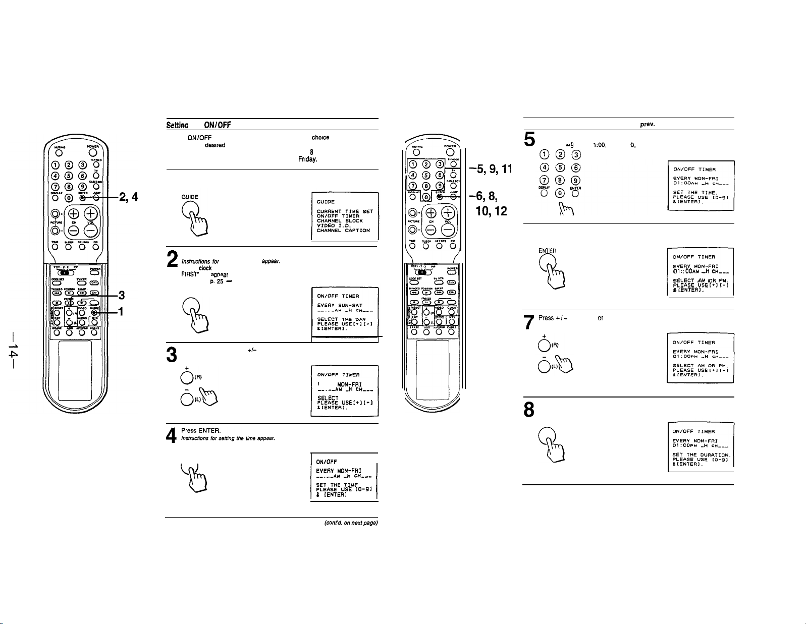
Settlna the ON/OFF TIMER
Set the ON/OFF TIMER to make the program of your choice appear on the
screen at the dewed time.
Example: Set the timer to turn on the N to channel 8 for 3 hours,
from 1:00 PM every Monday through Friday.
Press GUIDE.
Press repeatedly until the “ON/OFF TIMER” display turns red.
1
Press ENTER.
instruction*
2
(II the
FIRST will
Go back to p: iS - ‘Setting the Clock’.)
for
selecting the day appsar.
ckck
has not been set. the display ‘PLEASE SET THE CURRENT TIME
awear
on the screen.
ENTER
-5,9,11
458,
10,12
Setting the ON/OFF TIMER (cont’d. from prev. page)
5
Press For example, 0
- 9
to to set set the
190.
desired press time.
0.
1,
0 and
0. (You
000
Press ENTER.
6
ENTER
0
FL2
must
press 4 digits.)
I I
OWOFF TIMER
EVERY “ON-FRI
01 :ooAu -H CH--SELECT AM OR PM.
PLEASE “SEt+lt-I
8(ENTERI.
r-l
Press the AN WINDOW +I- buttons to select the day of the week.
(See illustration on p. 30)
3
ENTER
n
I
I
EYERY MON-FRI
--_-_A” Ai
SEl.ECT
PLEASE “SE*.>
DNlOFF
EYERY
--.--A” -” c*-..-
SET THE TIME.
PLEASE “SE to-91
L lENTERl
cue--
THE DAY
1-1
TIMER
Mm+FR*
I
I
I
-7
Press +I-
7
Press ENTER
8
ENTER
to set AM
clr
PM.
Page 15
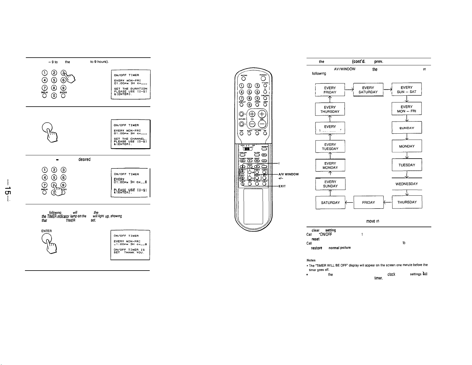
Press 10set the duration (up
9
Press ENTER
10
ENTER
Setting the ON/OFF TIMER (cont’d. from prev. page)
When you press AVIWINDOW + button. the selectable days will appear
the followmg order. (See Step 3.)
WEDNESDAY
m
Press 0 - 9 to set the dewed channel number.
ll
000
000
Press ENTER.
The followmg display will appear on the screen. and
12
t/E
T,,uER ,“dica,or lamp
fhal
the ON/OFF TIMER has been
0” me TV
will l&m up, show,“g
set.
EYERY MON-FRI
01:ooP” 3H c*_-s
SET THE CHANNEL.
PLE.GE USE
co-91
RESET
I
I
Press the A/V WINDOW - button to move m the reverse direction.
To clear the rettin9
Cal, the “ON/OFF TIMER” page (steps 1 and 2). Press RESET. then EXIT.
To reset the Setting
Cal, the
‘ON/OFF TIMER” page Press RESET. then repeat steps 3 to 12.
To re~lore the normal
Press EXIT.
-
If you unplug the TV. or a power failure occurs. both the
be erased. Reset the current time. then set the timer.
ptctvre
J
1
WEDNY
ckxk
and timer setbn9s &ill
j
Page 16
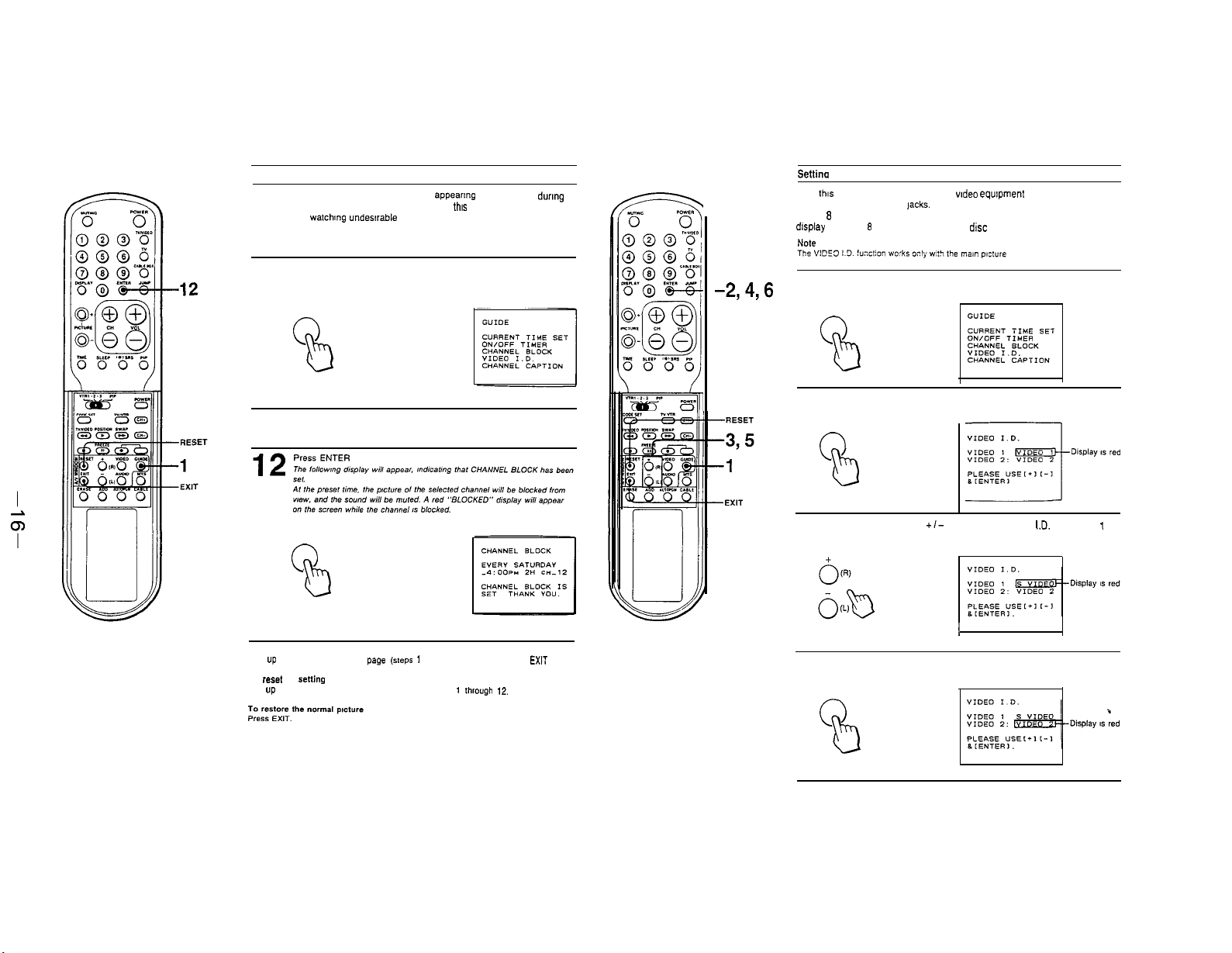
Setting CHANNEL BLOCK
CHANNEL BLOCK prevents a channel from appearing on the screen
the time that you set. We suggest that you use
children from watching undesirable programs.
Example: Set CHANNEL BLOCK for 1 hour. at 4:00 PM every Saturday. on
channel 12.
Press GUIDE.
Press repeatedly until the “CHANNEL BLOCK” display turns red
1
GUIDE
Same as “Setting the ON/OFF TIMER
this
function to prevent
dung
2-11
-2,4,6
Settina
VIDEO I.D.
Use this function to Identify the type of wdeo equpment connected to the
VIDEO 1 and VIDEO 2 IN lacks. You can change the VIDEO 1 display to
BETA. 8 mm, VHS, LD (laser disc player) or S VIDEO. and the VIDEO 2
display lo BETA, 8 mm. VHS or LD (laser disc player).
NOW
Press GUIDE.
Press repeatedly until the “VIDEO I.D.” display turns red.
1
GUIDE
Press ENTER.
2
ENTER
0
b
ENTER
0
PI
To clear the setting
Call up the “CHANNEL BLOCK” page (ste,x 1 and 2). Press RESET. then EXlT
To re*et the sening
Call UP the “CHANNEL BLOCK” page, then repeat steps
1
thrwgh 12.
Press the A/V WINDOW
3
Press ENTER.
4
ENTER
+I-
buttons to select the
I
1.0.
for VIDEO
J
1
Page 17
Press the AIV WINDOW
(See chart below).
5
+/-
buttons to select the I.D. for VIDEO 2
-3
-294,
638
Settina CHANNEL CAPTION
Use
this
function to caption each channel number display with the channel
call letters
(up
to lour
letters).
Press GUIDE.
Press repeatedly until the “CHANNEL CAPTION” display turns red.
1
GUIDE
Press ENTER.
2
ENTER
Settina the I.D.
Each time you press A/V WINDOW +, the I.D. will change m the followmg
order:
I
z
I.
VIDEO 1 I.D. Settings
VIDEO 1 j BETA + 8 mm + VHS + LD + S VIDEO
?
VIDEO 2 I.D. Settings
VIDEO 2 + BETA j 8 mm j VHS + LD
To move m the reverse direction
Press A/V WINDOW
TO reset the setting
Call the “VIDEO I.D.” screen. then repeat steps I To restore the normal
PlrsS EXIT.
-
6
p,cture
-5,7
-1
Press the 0 - 9 buttons to select the channel number you want to
caption.
3
Page 18
Press the AIV WINDOW
caption.
5
+/-
buttons to choose the first letter of the
Setting CHANNEL CAPTION (cont’d. from prev. page)
Press the AN WINDOW +I- buttons to choose the
caption.
9
third
letter of the
Press ENTER
6
ENTER
Press the A/V WINDOW +I- buttons to choose the second letter Of
the caption.
7
Press ENTER.
8
ENTER
(cont’d. on
next page)
--IFRET
.---
-9,ll
Press ENTER
10
ENTER
Press the AN WINDOW +/-buttons to choose the fourth letter of
the caption.
11
Press ENTER.
The channel caption Is set.
12
ENTER
To set more captions
Press A/V WINDOW +. then repeat steps 3 - 12
TO clear the setting
Cal, up the “CHANNEL CAPTION screen and press RESET, the” EXIT.
To reset the setting
Call up the ‘CHANNEL CAPTION” ~cree”. Press RESET, then repeat steps 3
TO restore the normal picture
press EXIT.
. If you want to leave a blank space an the channel number or caption. press ENTER
vatho”,
pressq AN WINDOW +I-
*
You can enter up to 32 channel captions.
t
-
12.
Page 19
1-8. ENJOYING OTHER USEFUL FEATURES
Muting the sound--MUTING Recewmo a Multichannel TV Sound program - MTS
Press MUTING.
me
display
JUMP
DISPLAY
“OL+
SLEEP
“MUTING”
To restore the sound
Press MUTING
Keepmg the channel displayed - DISPLAY
To display the channel
Press DISPLAY.
The mat” ,mcf”re mpur mode. channel captron,
Sound (MTS,. and Aclure-m-P,cfu,e r”,,“, mode
lew
*t?co”ds. men drsappear. me me,” p,cture ,nput mode wi,,
remal” on Ihe Screen
To turn off the display
Press DISPLAY agam.
Using the sleep timer - SLEEP
Turns TV
elf
aner
serri”g.
Press SLEEP
A green “SLEEP ON ” drsplay appears
for a ,a+
seconds.
A red “SLEEP ” display will appear I
the TV stlurs on.
To cancel the setting
Press SLEEP
A green “SLEEP OFF” display appears
OR
Turn the TV off.
The sleep rime, setd”~ will be cancelled
Switching quickly between 2 channels - JUMP
Press JUMP once to recall the channel
you were watchmg prevvxsly; press
JUMP
agam
feature to keep track of two programs
alternately.
-
Displaymg the current time -TIME
To display the current time
PressTIME.
will
appear on
the
sue”.
agam,
or press VOL +
aulomabcally approx,mate,y I hour
manure belore
agam.
to switch back. Use
lor
appronmately 3 seconds.
thls
Mulchaone,
w,,,
appear for a
TV
MUTING
0
b
DISPLAY
SLEEP
JVMP
0
b
TIME
n
-(OhsRS
--MTS
Each
f!m
you press MTS. the MAIN. SAP (Second Audio Program) and MONO modes
are selected in sequence. The display (in green) for each mode will appear on the
screen for
appnwmately
(NOTE: Dormg SAP modes. the sound will be muted.)
To listen to stereo sound
Press MTS lo select MAIN mode.
The MAlN display
The STEREO mdicafor lamp 0” the TV will ,,ghf up whenever a stereo broadcast
rece,ved.
MTS
&vi,!
a,,pea, 0”
3 seconds.
d%e
screen.
IS
MAIN
r-l
Notes
*A weak
Select
-
MTS
mcommg sqnal
MONO mode to
funclions
may cause
elimmate thw now.
only when the
excessive mxe
mam p~ture 1s m
with some stereo broadcasts.
TV mode.
Receivmg lifelike sound reproduction - (O)SRS
The Sound Remeva! System (SRS] aMows you lo select the sound mode you prefer
Each lime
youpress C.) SW. “(.)SRS
“C.)SRS
OFF’ modes are
In (0)SRS [AUTO] mode, SRS functions m both monaural and stereo modes.
Monaural sound programs will have a ‘simulated stereo’ effect.
In
(.I
SRS [STEREO] mode, SRS functions only when a stereo program
recewed.
selectedi”
[AUTO],”
sequence.
‘(.)SRS
[STEREO],” and
IS
Page 20

Troubleshootina
Disturbances I”
elimmated by checking the symptoms and followmg the
suggestions listed below.
F
Poor
(screen not lit), good
sound
Good p,ct”re, no sound
No
lit), no sound
No color
Snow and noise only
SYMPTOM
or no picture
picture
(screen not
picture
and sound can often be
l Adjust PICTURE.
*Adjust BRIGHT.
*Check antenna/cable
*Press VOLUME + on
l Press MUTING on the
.Check that the
*Check that the
*Check that “SPEAKER
*Check that the speaker
-1s
l Plug the unit Into a wall
-Check that the
l Is it a color program?
*Adjust COLOR.
l Is it an active or the
. Check the CABLE
*Check antennalcable
This 6
local Interference.
cars. neon
hardryers etc.) Adjust the
antenna for ml”lm”m
Interference.
CHECKANDADJUST
connections.
the N or VOL + on the
Remote Commander.
Remote Commander.
button 1s set correctly.
N/VIDEO button IS set
correctly.
MTS
ON” rs set.
cords are connected to
the SPEAKER termmals.
POWER switched on?
outlet.
TV/VIDEO button IS set
correctly.
correct channel?
setting.
connections.
often caused by
srgns,
(e.g.
Reflections from nearby
mountams or buildings
often cause this problem.
A
highly
directional
outdoor antenna 0, a
CATV cable may ,mp,o”e
the
p!cture.
Try
another channel.It
If the problem perststs, contact you, nearest serwce
facility.
c
ould
be station trouble.
-
Page 21

SECTION 2
DISASSEMBLY
*
2-l. REAR COVER REMOVAL
ear cover
@R
a.Two
our screws
OF
(BVTP4 x 16)
screws
(BVTP4 X 16)
2-2. Ul AND U2 BOARDS REMOVAL
@ Remove claw
\
@ Remove antenna terminal board
I
@ Remove claw
@ Remove Ul Board
I
@ Remove G bracket
2-3. SERVICE POSITION
0
Two special screws
(+Pw4
x 30)
-21-
Page 22

2-4. PICTURE TUBE REMOVAL
0
Anode cap
\
@ Two screws (BVTP4 X 16)
/
“CAU
TION”
TO
AVOID AN ELECTRIC SHOCK FROM CHARGED HIGH VOLTAGE OF PICTURE
l REMOVAL OF ANODE-CAP
Short circuit the anode of the picture tube and the anode cap to the metal chassis, CR
painted on the CRT, after removing the anode.
l
REMOVING PROCEDURES
@Turn up one side of the rubber cap in
the direction indicated by the
l HOW TO HANDLE AN ANODE-CAP
(j) Don’t hurt the surface of anode-caps with
sharp shaped material!
@ Don’t press the rubber hardly not to hurt
inside of anode-caps!
A material fitting called as shatter-hook
terminal is built in the rubber.
@ Don’t turn the foot of rubber over hardly!
The shatter-hook terminal will stick out or
hurt the rubber.
arrow @.
@Using a thumb pull up the rubber cap
firmly in the direction indicated by the
arrow @.
TUBE.
T
chield
or carbon
’ Anode button
@When one side of the rubber cap is
separated from the anode button, the
anode-cap can be removed by turning
up the rubber cap and pulling up it in
the direction of the arrow
0.
-22-
Page 23

SECTION 3
1
KV=27E$XR?z
SET-UP ADJUSTMENTS
l The following adjustments should be made when Perform the adjustments in order as follows:
a complete realignment is required or a new picture 1. Beam Landing
tube is installed. 2. Convergence
l
These adjustments should be performed with rated
power supply voltage unless otherwise noted. 4. White Balance
The control and switch below should be set as
follows unless otherwise noted:
PICTURE control
BRIGHTNESS control . . *. . . RESET position
Preparation:
l Set the side of the unit with the PICTURE
TUBE so that it faces east or west in order to
reduce the influence of external magnetic force.
.***********
To 80% (Full)
3. Focus
Note: Test Equipment Required.
1. Pattern Generator
2. Degausser
3. Digital multimeter
*
3-l. BEAM LANDING
1.
Input a raster signal with the pattern generator.
2.
Loosen the deflection yoke mounting screw, and set
the purity control to the center as shown in Fig.2.
3. Turn the raster signal of the pattern generator
to green.
4. Move the deflection yoke backward, and adjust
with the purity control so that green is in the
center and red and blue are at the sides evenly.
(Fig.3)
5. Move the deflection yoke forward, and adjust so
that entire screen becomes green. (Fig.1)
6.
Switch over the raster signal to red and blue and
confirm the condition.
7. When the position of the deflection yoke is
determined, tighten it with the deflection yoke
mounting screw.
8. When landing at the corners is not right, adjust
by using the disk magnets. (Fig.4)
purity control
Fig. 2
Fig. 3
Disk ma
rotatab
magnets correct
these areas (a-d).
nets or
f
e disk
-23-
Fig. 4
Page 24

f
3-2. CONVERGENCE
Preparation
l Before starting, perform FOCUS,
H.SIZE, V.LIN
and V.SIZE adjustments.
0
Set BRIGHTNESS control to minimum.
l Feed in dot pattern.
(1) Horizontal and Vertical Static Convergence
1
1
H.S
cl
(I v. STAT gagnet
4. When the V.STAT magnet is moved in the
direction of arrow @ and @, red, green and blue
dots move as shown below.
J
-
RV701
G2(SCREEN)
FOCUS
1. Adjust H.STAT VR to converge red, green and
blue dots the in center of the screen. (Horizontal
movement)
2. Adjust V.STAT magnet to converge red, green
and blue dots in the center of the screen.
(Vertical movement)
3.
If the red, green and blue dots do not converge in
the center of the screen with H.STAT VR,
perform horizontal convergence adjustment using
H.STAT VR and V.STAT magnet as shown
below. (In this case, H.STAT VR and V.STAT
magnet effect each other.)
l Tilt the VSTAT magnet and adjust static
convergence to open or close the V.STAT magnet.
If the blue dot do not converge with red and green
dots, perform following steps.
l HMC and VMC correction for BMC (Hexapole)
Magnet
1. HMC (Horizontal Mis-convergence) correction
and motion of the Electron Beam with the BMC
Magnet.
HMC correction (A)
RG
00 0
B
HMC correction (B)
IR
.>B
0 00
000
=B
GB
h--P
R % B
-24-
Page 25

2. VMC (Vertical Mis-convergence) correction and
motion of the Electron Beam with the BMC Magnet.
VMC correction (A) VMC correction (B)
,
Purity
C<D
C=D C>D
C=D
(2) Dynamic Convergence Adjustment
Perpartion :
l Before starting perform Horizontal and Vertical
Static convergence adjustment.
1. Slightly loosen deflection yoke screw.
2. Remove deflection yoke spacers,
Yoke
screw
3. Move the deflection yoke for best convergence as
shown below.
4. Tighten the deflection yoke screw.
5. Install the deflection yoke spacers.
BGRRGB
~o-o-0
-25-
Page 26

,
(4) Screen-corner Convergence
Affii a Permalloy
misconverged areas.
b
d
ass’y
corresponding to the
3-3. FOCUS
1. Tune in an off-air signal.
2. PICTURE -control to 80%.
3. Adjust the focus VR on A board so that the
focus at the center of the screen is optimum.
A magenta ring will appear if the focus is
adjusted only in the center of the screen.
Adjust evenly throughout the entire screen.
FOCUS
3-4. G2 (SCREEN) AND WHITE BALANCE
ADJUSTMENTS
1. C2 (SCREEN) ADJUSTMENT(RV701)
1) Set the PICTURE and BRIGHTNESS to normal.
2) Confirm Gl voltage is within 30.0&5V.
3) Apply DC voltage of 180V to the cathodes of R,
G and B from DC stabilized power source.
4) While watching the picture, adjust the G2 control
(RV701) to the just the retrace line disappears.
(Using the Remote Commander)
2. WHITE BALANCE ADJUSTMENTS
Set to service mode.
1)
Press
2)
necessaries “TRINITONE” set to “LOW” by q
or
Input an entire white signal.
3)
Set the PICTURE to minimum.
4)
Select S BRT with mand 1 , and then set the
5)
level to minimum with 1 and
6)
Select G CUT and B CUT with 1 and m.
And adjust the level with m and m for the best
white balance.
7) Set the PICTURE to maximum.
8) Select G AMP and B AMP with 1 and 4, and
adjust the level with @
balance.
9) Write into the memory by pressing IMUTING]
then [ENTER].
3. SUB BRIGHT ADJUSTMENT
1) Set to service mode.
2) Input a staircase signal of black and white from
the pattern generator.
3) BRIGHTNESS
PICTURE * * * * * . * . .
4) Select S BRT with m and m , and adjust SUB
BRIGHT level with Hand B so that the stripe
second from the right is dimly lit.
/=J
I=]
.
-+
-1
***
RESET
minimum
to normal and if
@
and H for the best white
---f
-26-
white
second f
ram
the right
Page 27

c
a. METHOD OF SETTING THE SERVICE MODE
Press
~
button on the Remote Commander
while pressing switch on the rear of the set.
Service modeswitch
\
-;
b. ADJUST BUTTONS AND INDICATOR
-
MUTING
POWER
c . AN ITEM OF ADJUSTMENT
NAME REGISTER
T
VP
VP
VP
lzz$--
VP
VP
d. METHOD OF CANCELLATION FROM SERVICE
MODE
Set the standby condition (Press
on the commander) in the next place, press
-1
button again, hereupon it becomes TV
mode.
e. METHOD OF WRITE FOR MEMORY
1) Set to Service Mode.
2) Press H (UP) and m (DOWN), select an item of
adjustments.
3) Press
-1
(RED)
button indicate WRITE
on screen.
4) Press ENTER button to write for memory.
this time WRITE (YELLOW) is indicated on
screen.)
m
button
(At
VIDEO
RESET
-
ENTER
-MTS
1000 0000
f . MEMORY WRITE CONFIRMATION METHOD
1) After adjustment, pull out the plug from AC
outlet, and next place, plug in AC outlet again.
2) Turn the power switch ON and set to Service
Mode.
3) Call the adjusted items again, confirm they were
adjusted.
qiizq
W RITE
’
piEi]
1
RED
YELLOW
-27;
Page 28

SECTION 4
SAFETY RELATED ADJUSTMENTS
Note: Test Equipment Required.
1. Ammeter
2. DC Power Supply
3. Digital multimeter
4. Audio OSC
5. Valiable auto-transformer
ABOARDANDCBOARD
E
R559 CONFIRMATION METHOD (HOLD-DOWN
CONFIRMATION) AND READJUSTMENTS
The following adjustments should always be performed when replacing the following components
(marked with 0 on the schematic diagram).
A BOARD :
0
1. Preparation before confirmation
1) Remove R675 on the G board and connect a
variable resistor (RVl : about 10kfi ) between
pin 0 of IC653 and B+ line.
2) Supply 120+2.OV AC to with variable autotransformer.
2. Hold-down operation confirmation
1) Turn the POWER switch ON, and input an
entirely white signals and adjust ABL current to
1650 +80 PA with PICTURE and BRIGHT etc
controls.
2) Increase B+ line voltage gradually by adjusting
the resistor of RVl. Confirm that the minimum
voltage is less than
raster disappears during operation of hold-down
circuit.
NOTE: When the hold-down circuit starts
3) Turn the POWER switch ON, and input a dot
signals and adjust ABL current to 150+50pA
with PICTURE and BRIGHT etc controls.
4) Increase B+ line voltage gradually by adjusting
the resistor of RVl. Confirm that the minimum
voltage is less than
raster disappears during operation of hold-down
circuit.
NOTE: When the hold-down circuit starts
PM501,Q608,Q607,R629,R628,R627,R559
143.5V
DC whereby the
operating, switch
the set immediately.
operating, switch
the set immediately.
OF’F
the POWER of
146.5V
DC whereby the
OFF
the POWER of
0
3. Hold-down readjustment
When step 2 is not satisfied, readjustment should
be performed by altering the resistance value of
R559 (a component marked with
q
>. T500;
FBT;
i
;
*
-2%
Page 29

Page 30

SECTION 5
CIRCUIT ADJUSTMENTS
5-l. ELECTRICAL ADJUSTMENT BY
REMOTE COMMANDER
Use of Remote Commander (RM-Y 111) can
be performed circuit adjustments about this model.
1.
METHOD OF SETTING THE SERVICE MODE
1) Press
-1
button on the Remote Commander
while pressing switch on the rear of the set.
*
NOTE : Test Equipment Required.
1. Pattern Generator
2. Frequency counter
3. Digital multimeter
4. Audio OSC
Service mode switch
-
2. ADJUST BUTTONS AND INDICATOR
MUTING
item
SERVICE HFRE 0
SERVICE HFRE 0
I
dqta
ii
0
0
MAIN--MT SMAIN--MT S
11
SAPSAP
11
MONOMONO
I
VIDEO
RESEl
Page 31

3. AN ITEM OF ADJUSTMENT
TEM
HFRE
dFRE
vpos
VSIZ
VLIN
vsco
HPOS
HSIZ
PAMP
CPIN
PPHA
VCOM
GAMP
BAMP
GCUT
BCUT
CROM
SPIX
SHUE
SCOL
SBRT
RGBP
EFERENCE
ATA
44
09
10
1D
07
08
07
11
OF
04
07
02
17
18
OD
09
1B
33
23
1c
3F
1E
q--
NAME REGIST
dP
JP
dP
dP
rlP
dP
VP
VP
dP ‘IN AMP.
VP
VP
VP
VP
VP
VP
VP
VP CHROMA TRAP
VP
VP HUE
VP
VP BRIGHT
VP
i-FREQUENCE
J-FREQUENCE 1
J-SHIFT
J-SIZE
J-LINEARITY
;-CORRECTION
i-PHASE
i-SIZE
tORNER PIN
‘IN PHASE
d-COMP
SREEN AMP.
BLUE AMP.
GREEN CUT OFF
BLUE CUT OFF
PICTURE
COLOR
RGB PICTURE
4. METHOD OF CANCELLATION FROM SERVICE
1
1
Set the standby condition (PressIPOWERjbutton on
the commander) in the next place, press
MODE
*
-1
button again, hereupon it becomes TV mode.
5. METHOD OF WRITE FOR MEMORY
1)
Set to Service Mode.
2) Press
!$l
(UP) and m (DOWN), select an item of
adjustments.
3)
Pressmlbutton
indicate WRITE(RED)
on screen.
4)
Pressmlbutton
to write for memory.
(At
this time WRITE (YELLOW) is indicated on
screen.)
6. MEMORY WRITE CONFIRMATION METHOD
WRITE
MPX
FILO
DEEM
STEV
SAPV
PILO
SEP
VD
LVOL 00 AP
RVOL 00 AP VOLUME-R
SHAR
DISP
08
1B
07
21
1F
08
1B
6A
07
37
AP
AP
AP I2
AP
AP
AP PILOT
AP
AP
VP
VP PWM OUTPUT
ATT
’
I1
OSCl
osc2
WIDE BAND
SPECTRAL
VOLUME-L
SHARPNESS
7. ADJUSTMENT WHEN REPLACING IC
1)
IC 102(PCD 8582)
EXCHANGE
ADJUSTMENT
EXCHANGE
ADJUSTMENT
ALL SERVICE LIST
1) After adjustment, pull out the plug from AC
outlet, and next place, plug in AC outlet again.
2) Turn the power switch ON and set to Service
Mode.
3) Call the adjusted items again, confirm they were
adjusted.
SET TO SERVICE MODE
IC lOl(M 37100 M 8)
EXCHANGE EXCHANGE
ADJUSTMENT
(PWM OUT)
1000 0000
l-----l
IC SOl(CXA 1313 S)
ADJUSTMENT VP
(HFRE-RGBP,
VSHO-ABLM)
WRITE THE MEMORY
TURN THE POWER SWITCH OFF.
CANCEL THE SERVICE MODE
NOTE : If service mode is canceled before writing into memory,
the adjustment data is not recorded.
Please write into memory, after adjustment.
-32-
Page 32

2) The following initial setting should always be performed when replacing the IC 102 (PCD 8582).
ITEM
VSOM
AFC
REF
ROFF
GOFF
BOFF
ABLM
TEST
DRGB
NAME REGISTER
r;
VSMO
VP
AFC 1.0
VP
VP
VP
VP
VP
VP
AP
VP
REF 1.0
OFF NR
OFF NG
OFF NB
ABLM
T
DRGB
T-
I
4DJUSTMENT
0
0
2
1
1
1
1
0
1
i
IV.FREQUENCY
1) Set the Service Mode.
2) Input an off-air signal (VID’EO IN -+ no signal).
3) Connect the frequency counter across connector
4) Select VFRE withmandm.
5)
6) Write the memory by pressing
ICHROMA
1) Set to Service Mode.
2) Input a color-bar signal.
3) Select NOTCH (VIDEO condition),
*Please with the memory each items by pressing
-I+
5-2. A BOARD ADJUSTMENTS
and then
pressI=].
4) Connect an oscilloscope to pin 0 of A-32
5) Select C ROM
Q501 o
6) Write into the memory by
A-31
A-52
pi?zz?
A-55
pTGiiq
7) Set NOTCH to OFF, and make normal condition
A-32
A BOARD
-component side-
IF 201
ADJUSTMENT
(VFRE)~
VDY - @of A-52 connector and ground.
AdjustHandmto
pmzq
.
TRAP ADJUSTMENT
the 56
k0.5
Hz.
m]
(CROM)]
+ then
turn ON by
press-ing q .
And then set the COLOR VR to
maximum set-ting position and SHARPNESS
control to center.
connector and ground.
withiandm,
and then adjust 3.58
MHz (CHROMA) ingredient is minimum with B
andd.
pressing-]-+
then
F-1.
with-1
--+
then RESET
I*
IRF
AGC
ADJUSTMENT(IF
BLOCK VR)I
1) Input a color-bar signal.
2) Adjust AGC VR of IF 201 so that snow noise and
cross-modulation disappear from the picture.
3) Confirm them at every channel.
IH.FREQUENCY
ADJUSTMENT
(HFRE)~
1) Set to Service Mode.
2) Input a color-bar signal.
3) Connect a frequency counter to base of Q 501.
4) Call the item of AFC, set to 3 level (free run).
5) Select HFRE
6)
Adjutiandato
7) Call the item of AFC again, adjust the level“ 00
withland1.
the 15735+ 60 Hz level.
“.
8) Write into the memory by pressing -1-+
then
-1.
-33-
Page 33

/SUB
CONTRAST ADJUSTMENT
1) Set to Service Mode.
2) Input a color-bar signal. (75 IRE)
3) Set the conditions as follows.
PICTURE
COLOR
R OFF
G OFF
B OFF
press-1
+
Selecta (ON) and@ (OFF) withMandw.
......... MAX
.........
.........
.........
.........
MIN
ON
OFF
OFF
(L) (It becomes minimum) .
(SPIX)]
ISUB
HUE, SUB COLOR ADJUSTMENT (SHUE, SCOL)]
1) Input a color-bar signah
-+
2)
Press-\
3) Set to Service Mode.
4) Connect an oscilloscope to pin
and ground.
5)
AdjustMandmto
to SHUE and SCOL
Vl v4
T
-A
then RESET to normal.
the
Vl=V4
withmandM.
v2 v3
LLL
and
@of
connector A-32
V2=V3
by select
white
Connect an oscilloscope to pin 0 of connector
4)
A-32 and ground.
Adjust 1 and H to the 1.7 + O.lVp-p level by
5)
select-ing SPIX withmandB.
Write the memory
6)
IENTER~
.
7) Return the following back to normal after
adjustment.
G OFF
B OFF
COLOR
PICTURE
bypressing 1-1
.........
.........
......... CENTER
.........
ON
ON
80%
-+ then
6) Write into the memory by pressing
p7mEiq.
IV.SIZE
ADJUSTMENT (VSlZ)\
1) Set to Service Mode.
2)
Pressml + then-/to
3) Input a cross-hatch signal.
4) Adjust i and i to the best vertical size by selecting
VSIZ
5) Write
withmandm
intoThe mymory
.
by pressing
(MUTING]
normal.
-1
-+then
-+then
$NTER] .
IH.SIZE
ADJUSTMENT (HSIZ)]
1) Input a cross-hatch signal.
2)
Press-1
3) Set to Service Mode.
4)AdjustIandmto
withIand1.
5) Write into the memory by pressing
-+ then-It0
best horizontal size by selecting HSIZ
normal.
IR/IUTING\ --*then
-34-
Page 34

-___
--------
KV-Z/ tAKY9
RM-Ylll
IH.CENTER
ADJUSTMENT (H
POS)]
Note: Perform this adjustment after H.FREQUENCY
ADJUSTMENT (HFRE) .
IFILTER
1) Set to Service Mode.
2) Select tolTEST[withmandi, set the data to “1”.
1) Input a color bar signal.
2)
Set the Service mode.
3) Select HSIZ
4)
Pressa
5) Adjust A-55
with1 andi
so that the Horizontal size set to min.
conector
.
position so that both-size
3) Connect an audio oscillator to R116 using a
branking width of the Raster should be same on the
Scrnne.
6) Unplug Set then plug in Set.
7)
Set to Service mode.
8) Select HPOS
withmandw
.
9) Adjust H and 8 so that the color bars center should
be set to the CRT Screen center position.
10) White into the memory by the pressing-1
-+ then ENTER
I*
ADJUSTMENT
(MPX, FILO)]
Then select MPX and change data to “08” .
capacitor (10~
kHz+O.l
And then, through the
kHz.
F/16V),
set frequency to 62.936
lOkS2
resistor, feed 9.3V
into the pin @ of VIF pack.
audio oscillator
V 4fh : SINE-WAVE 62.936 KHzkO.1 KHz
LEVEL 3.0 Vp-p
4) Make the data
and m And then, send up the data gradually by
PIN AMP (PAMP) , CORNER PIN (CPIN) AND PIN PHASE
(PPHA) ADJUSTMENT
1) Input a cross-hatch signal.
2)
Press-1
3)
Set to Service Mode.
4) Select PAMP, CPIN and PPHA
5)
Adjustaandmto
6) Write the memory
-+
thenmlto
normal.
the best picture.
by-1
(ENTER].
withmanda.
+
pressing w . Set the data to Dl before SAT3
changing to 1 from 0.
5) Send up the data gradually. Set data D2 when
SAT3 changes 0 from 1.
6) Adjust the data of FILO to D ’ :
7) Write into the memory by pressing-1-+
thenmTER1 .
PIN AMP
CORNER PIN
“00” by selecting FILO with
D 2
item
I
SERVICE
1000 0110 MONO
!iILO
\
/
SAT3
I
21
a
.
data
-35-
Page 35

IST
VCO ADJUSTMENT (MPX,
1)
Set to Service Mode.
2) Select TEST with @ and 1, set the data to “1”.
And then press
3) Select MPX, set the data “8” .
4) Connect an audio oscillator to R 116 using
electrolytic capacitor (10~
frequency
of VIF pack using
audio oscillator
5) Select STEV withiand@, set the data to “00”
withI.
the data to Dl before SAT2 changes from 0 to 1.
6) Send up data gradually, set the data to D2 when
7) Adjust the data of STEV to
8) Write into the memory by pressing
And then, send up the data gradually. Set
SAT2 changes 1 from 0.
then-1
m]
VST.
Then, apply DC voltage to pin
lOk0
Q%-
V 4 fh : SINE-WAVE 62.936 KHz zk 0.1 KHz
LEVEL 3.0 Vp-p
.
STEV)]
to MONO.
F/16V)
connect to 9.3V line.
TP21(MPJ(I
and appply the
from
9.3V
I
ll
.
-1
@
line ,
10 K
-+
[MPX IN LEVEL ADJUSTMENT (MPX)]
1) Set to Service Mode.
2) Select TEST with1 and @, set the data to “0”
withw. And then
3) Select MPX with m and w, set the data to “08”
withHandw.
4) Write into the memory by pressing
then-1
[PILOT CANCEL ADJUSTMENT (PILO)]
1)
Set to the Service Mode.
2) Select TEST with fl and H, set the data to “0”
with H. And then
3) Select
withmandm.
4) Write into the memory by pressing
+ then-1
ISAP
VCO f (ADJUSTMENT
1) Set to Service Mode.
2) Input a stereo broadcast signal with SAP.
3) Select TEST with m and B, set the data to “0” .
And then, press (MTSlto MAIN.
4) Connect a digital multimeter to TP-l(DBX).
This voltage reading will equal V 1.
5) Press MTS to SAP and this voltage will equal V 2.
6) Select SAPV withmandm, adjust@andwso that
V 2=V 120.03 VDC.
7) Write the memory
.
PILO
withmandH, set the data to “08”
*
press[MTSlto
press[MTSlto
.
(SAPV1]
by-1
-1
MONO.
m
MAIN.
IR/IUTINGI
-+
.
-+
10000010
MONO
data
ISEPARATION
1) Set to Service Mode.
2)
Pressmlto
-cast signal.
In the next step, receive a stereo broadcast signal.
3) Select SEP and VD with 1 and H, adjust 1 and
so that a clear stereo sound is effected.
ADJUSTMENT
MAIN and receive a monoral broad
(SEP)\
-36-
@
Page 36

5-3. P BOARD ADJUSTMENTS
RV 2107 RV 2103
pzzlcoLJ
?V 2106
;usHUE]
Q
Q
RV 2108
CoNTl
8
lposll@ @
RV 2105
-1
P BOARD 0 TP
-component side-
RV 2200
(B-y(
TP4:R
R-Y
FL 2205
p5iriE$
FL22o6
0
Y-IN
0 TP46B
13 a
[RF AGC ADJUSTMENT(IF BLOCK VR)]
1) Input a color-bar signal.
2) Set to PICTURE IN PICTURE mode.
3) Adjust AGC VR of IF 1201 so that snow noise and
cross-modulation disappear from the picture.
4) Confirm them at every channel.
@
RV 2201
(R-YI
TP047
B-Y B OUT
p+7iGm@
0
B
ISUB
HUE ADJUSTMENT(RV
2106)j
1) Input a color-bar signal.
2) Set to PICTURE IN PICTURE mode.(
l/4
SIZE)
3) PICTURE ............ 80%
BRIGHT
COLOR
HUE
. . . . . . . . . . . .
. . . . . . . . . . . .
. . . . . . . . . . . .
RESET
RESET
RESET
4) Connect an oscilloscope to TP-47 B.
5) Adjust RV2106 so that the 0 coincides with
@as
shown in figure.
1 CONTRAST ADJUSTMENT(RV
2108)l
1) Input a color-bar signal.
2) Set to PICTURE IN PICTURE mode.
3) Observe signal at TP-13 a an oscilloscope.
4) Adjust RV 2108 (SUB CONT) so that the signal
level between white and pedestal becomes 550 + 10
mVp-p
as shown.
[SUB COLOR ADJUSTMENT(RV 21071
1) Input a color-bar signal.
2) Set to PICTURE IN PICTURE mode.
3) COLOR
HUE
. . . . . . . . . . . .
. . . . . . . . . . . .
RESET
RESET
4) Connect an oscilloscope to TP-47 B.
5) Adjust RV 2107
so that voltage is 0.9
+0.05
Vp-p.
[BRT LEVEL ADJUSTMENT(RV 2105)j
1) Input a color-bar signal.
2) Observe PICTURE IN PICTURE mode.
3) Adjust RV
2105(B.LEVEL)so
that the signal level
between C.B.black level and Sync level becomes
same level as shown.
TP-13 a output
LEVEL
0-Y
.OSVP-P
-37-
Page 37

KV-27
E&FN~ (
IA/D OFF
B-Y ADJUSTMENT
1) Input a color-bar signal.
2) Set to PICTURE IN PICTURE mode.
3) Connect an oscilloscope to TP-46 B.
4) Adjust RV 2200 so that the wavefront as shown in
SET ADJUSTMENT(RV
figure.
2200,2201)]
ISUB
PICTURE ADJUSTMENT(FL2205,2206)1
1) Input a monoscope signal.
2) Set to PICTURE IN PICTURE mode.
3) Adjust FL2205,FL2206 so that A and B are same
size.
B - YQ 4-b
Q -Iv-
picture blue
picture white
picture green
@-I
R-Y ADJUSTMENT
1) Input a color-bar signal.
2) Set to PICTURE IN PICTURE mode.
3) Connect an oscilloscope to TP-46 R.
4) Adjust RV 2201 so that the wavefront as shown in
figure.
t
A
FL-2205=B side
FL-2206=A side
[SUB PICTURE POSITION ADJUSTMENT(RV 2103)]
1) Input a cross-hatch signal.
2) Set to PICTURE IN PICTURE mode.
3) Adjust RV 2103 so that the SUB PICTURE is a
suitable position.
B
B
-YQ
4-L
@--Iv-
8 7
picture red
picture white
r
picture green
-38-
Page 38

Page 39

Page 40

Page 41

Page 42

Page 43

Page 44

Page 45

Page 46

‘.
SEMICONDUCTORS
6-4
CXAll14P NJM2245S
TA8601BN-FA-1
s6
KV47EXR95
RM-Ylll
clPC66 1 G
19
2SC2611
2SC2688-LK
LETTER
SIBE
MA
KW27EXR95
152WK
RM-Ylll
SEL 1
ZZZR-C
123456799
RC4558P
a
CXAl264AS 2Sf11408-Y
lToP VIEW
CXA1313S
4a
CXAl3lSP
MB88201-638L
SN74LS123N
SN74LS 19AN
lb 9
25
24
7 6 5
~
1234
mP
VIEW
RC78MOSFA
RC7809FA
SBX1681-02
SBX
1483-59
1
TfIA2009A
TflA8 172
fiPC78NOSH
0
10
ITOP
VIM
lrPf)69OlG
2SA1091-0
2SC2551-0
2SAl 162-G
2SCl623-L5L6
2SC2713-L
2Sfll886CA
EGP2OG
ELlZ
ERB91-02
&
MNl280-S
SE-13SNS
pPC7893HF
2SA1175-HFE
2SC2785-HFE
PC81 7-C
PS2501-1LB
N
-lII!l
RBV-406H-01
6-l
Rfll OESBZ
RO
12ESB2
Rfll8ESBl
Rfll8ESB2
Rf124ESB
RfI33ESB2
Rf)S. 6ESB2
RfiI6.2ESB2
Rf19.1ESB2
WG7 13A
lSSl19
lSVl13
SlVB40
t
n
UOSG
HOSE
OaE
1
M37100M8-C16SP
64 33
1
ITOP
VIM
32
STR-S630 1
-67-
2SA937-Q
2SC2673-Q
ERB93-02
RS3FS
RU-1P
RU-3AM
RU-30A
RU4QS
ANOSE
4
CATHOSE
ANO9E
Q
Rfll2M-Bl
RQ3.6M-Bl
;xlz. l$l3:
.
CATtioE
-
-68-
Page 47

SECTION 7
EXPLODED VIEWS
NOTE:
*
Items with no part number and no
cription are not stocked because they
are seldom required for routine service.
*
The construction parts of an assembled
part are
number in the remark column.
indicated with a collation
des-
7-1. CHASSIS
0
: BVTP3 X 12 7-685-648-79
H
: BVTP4X 16 7-685-663-79
*
Items marked ' *
they are seldom required for routine
service. Some delay should be anticipated
'
are not stocked since
when ordering these items.
.
.................. .... .. .... ..... ....
................ ... ... .. ..... .....
................
......................................
.......................................................................
:::::::
::::i
zt:
The
c~rnp~nents
$$
shad<og
I%$ Cal
::::::5
$jj
12:
::>:::
::::~:::.z:.:.:.:.:.:.:.:.:.:.:r:.:.:.:.:.:.:.:.:.:
.............................
‘.:.“F:.:.:.:.:.: :.:.;.:.:.;
.
........................................................
.......
g &es c~mposants
I$$$ une
$$ h sent d’une
8
1$11x les
il)i; pi?xesde w-&o
:s+iiiiii>i:.
............. ......
...............
and mark a are
for
safety
Replace only with part
specified
.....................................
...‘:.:: .:,.,:
::::.~~::::;::.~:::::::::::::::::::.:.::::::::::::::::::‘:.:.:.:.:.:.:.:
................................................
. .................................
critique pour la s&wit6
........
.
. .
:,:,:,:,‘:::::i::::::::::::::.::::::::::::::::::.::::::::::::?
trame et par
remplacer
..........................
...................................
.....................................................................................................
. .
...........
.. ...............................
..\..........
................................
..
Identified by g r
....................................
(0.:
..................
identifies
importance $$
que
sticifiP
:.:.:.:.:.:.;.
....................
::
............. .
..................
~.~.~.‘”
crit:
numba! g,$
.:.
:.:.:.:.:.:.~.~.~
::,:,:,:,:,:,:,:,:,:,::,:,:,:,:,:,~
pa> :.:
une marqlM ;$$
NP: ,j;,i
par
deb 1:;:;:
.........
.)):.:.:.:.:.:.:(:
:.j:.:.:.):
...................
.:tt,f,
.::::2
1
;g,
.......
3;;;
:::::.,
;;g;
::>+....................................................
*
::::;:
...
.:+:
::::.4
:::::i
,,,,,_
REF NO PART
i;
14
I5
NO
*i-556-945-21
l-561-306-00 JACK, PIN
DESCRIPTION
CABLE, P-P
*A-1394-314-A U1 BOARD. COMPLETE
*4-397-418-01
*l-637-487-41 U2 BOARD
RIVET,
T'TYPE
(F)
REMARK IREF.NO PART NO.
I
I
I
I
-69-
DESCRIPTION
TEHMINAL BOARD, ANTENNA
LABEL (A), ANTENNA
COVER SUB
BOX (TOP)
ASSY,
REAR
(R) ASSY,
SPEAKER
SCREW, STEP HILO TAPPING
BOX(BOTTOM) (RIGHT)ASSY,SPEAKER
BOX (TOP)
B~~(B~TT~M)(LEFT)ASSY, SPEAKER
CUSHION (A)
CAP, ELECT 4.7KF
SPEAKER
(L) ASSY,
SPEAKER
20%
SPEAKER
SCREW, TAPPING. HEXAGON HEAD
STICKER, SONY SYMBOL
LABEL, CAUTION
(50)
REMARK
24
24
5OV
Page 48

KV-27 E$Fi?:
7-2. PICTURE TUBE
a: BVTP3X12
A:
BVTP3X
16
’
I
7-685-648-79
7-685-650-79
65
AEF
Nil PART NO DESCRIPTION
REMARK
JREF.Nfl
I
PART NO.
*$-371-629-01
4-390-505-01
*4-~38'7-284-01
4-033-681-01
4-308-870-00
1-452-032-00
I-452-094-00
X-4306-312-0
3-704-495-01
*l-637-952-22
8-741-681-02
---___ I------- --------
-7o-
DESCRIPTION
STIIPPEH, WlHE
SCREW
(7),
HfllDFH LFAD
HiUiR: LiAD
CLIP LEAD WIRE
MAGNi'T,
MAGNET, ROTATAHLE DISK:
P)?RMALLLlY
;PKmb
IC SHXl681-02
TAPPING
DISK;
DY
1OMM b
ASSY, CONVERGENCE
15MM d
HEMAHK
_...~_
Page 49

SECTION 8
ELECTRICAL PARTS LIST
NOTE:
*
Items marked ' * ' are not stocked
since they are seldom required
routine service. Some delay should be
anticioated when orderina these items.
. All variable and adjustable resistors . MF : pF, PF :
have characteristic curve B. unless
otherwise noted.
RESISTORS
*
All resistors are in ohms
'F:
nonflarnrllable
When indicating parts by refer-
CAPACITORS
l
The components identified by q in this manual
have been carefully factoty-selected for each set in
orderto
satisfy
Should replacement be required, replace only with
the value originally used.
wP
regulations regarding X-ray radiation
COILS
*
MMH :
lnH,
UH : MH
REF NO. PART NO.
*A-1195-038-A P BOARD, COMPLETE
*3-738-015-01 COVER, (DIA. 6) CARBON VR
*4-363-404-00 HOLDER,
C2000
I-124-907-11 ELECT
c2001
l-163-009-11 CERAMIC
C2002
I-126-101-11 ELECT
c2101
I-163-125-00 CERAMIC CHIP 220PF
1-164-232-11 CERAMIC CHIP O.OlHF
c2102
C2103
l-124-907-11 ELECT
I-124-907-11 ELECT
;;g
l-124-907-11 ELECT
C2lU6
I-163-009-11 CERAMIC CHIP
l-124-499-11 ELECT
r2107
C2108
1-124-499-11 ELECT
1-124-499-11 ELECT
C2109
C2110
I-163-107-00 CERAMIC CHIP 39PF
l-124-907-11 ELECT
1;;;;;
l-130-483-00 MYLAR O.OlMF
C2120
1-163-125-00 CERAMIC CHIP 220PF
C2121
1-164-161-11
l-163-125-00 CERAMIC CHIP 220PF
C2122
l-163-009-11 CERAMIC CHIP
:;i;:
l-124-903-11 ELECT
C2126
I-124-907-11 ELECT
I-163-117-00 CERAMIC CHIP
C2!27
l-124-902-00 ELECT 0.47MF
%
l-163-105-00 CERAMIC CHIP 33PF
l-163-103-00 CERAMIC CHIP 27PF
C2130
I-163-093-00 CERAMIC CHIP IOPF
C2131
l-124-907-11 ELECT
c2132
1-163-115-00
C2133
C2134 l-163-115-00 CERAMIC CHIP 82PF
C2135
l-163-123-00 CERAMIC CHIP
l-163-115-00 CERAMIC CHIP UpW;
C2136
l-124-034-51 ELECT
x
l-163-109-00 CERAMIC CHIP 47PF
I~2139
I-163-093-00 CERAMIC CHIP
l-164-232-11 CERAMIC CHIP O.OlMF
C2140
I~2141
1-124-768-11 ELECT
l-163-037-11 CERAMIC CHIP
C2142
C2143
l-124-477-11 ELECT
l-124-907-11 ELECT
%i
l-130-476-00 MYLAR 0.0027MF
C2146
F%
i2150
-163-809-11 CERAMIC CHIP 0.047MF
-164-232-11 CERAMIC CHIP O.OlMF
-164-232-11 CERAMIC CHIP O.OlMF
-163-037-11 CERAMIC CHIP 0.022MF
DESCRIPTION
-----------
tt*tt****t*******
<CAPACITOR>
CERAMIC CHIP
CERAMIC
IC
1OMF
CHIP ~b;JXlbMF
K
1OHF
Ili;OIMF
IMF
IWF
IOMF
0.0022NF
;i.$OIMF
1OMF
1OOPF
IOMF
CHIP
82PF
180PF
1OPF
4.7MF
Oqj.U;2MF
1OMF
REMARK
------
zi:
16V
5ov
5ov
55;;
5ov
5ov
5ov
%:
5ov
5OV
5ov
5:;
5ov
%
5ov
5ov
55:':
5ov
5ov
;;i
5ov
5ov
%
5ov
25V
.F.NO.
PART NO.
---- --------
2151
I-123-382-00 ELECT
12152
l-163-023-00 CERAMIC CHIP
:2153
l-136-165-00 FILM
12154
I-136-169-00 FILM
:2155
l-124-902-00 ELECT
2156
l-124-925-11 ELECT
:2157 1-164-161-11
:2158
l-163-109-00 CERAMIC CHIP 47PF
:2162
I-163-123-00 CERAMIC CHIP 180PF
:2163 I-163-123-00
:2164
l-163-123-00 CERAMIC CHIP
:2176
l-163-009-11 CERAMIC CHIP
:2178
l-124-034-51 ELECT
:2179
l-124-034-51 ELECT
:2181
l-164-232-11 CERAMIC CHIP
:2182
l-124-477-11 ELECT
:2200
1-164-232-11 CERAMIC CHIP
:2201
l-124-907-11 ELECT
:2202
l-163-009-11 CERAMIC CHIP O.OOlMF
:2205
1-164-232-11 CERAMIC CHIP y.$lMF
:2206
l-124-903-11 ELECT
:2207
l-164-232-11 CERAMIC CHIP O.OlMF
Z2208
1-164-232-11 CERAMIC CHIP O.OIMF
Z2209
l-163-129-00 CERAMIC CHIP 330PF
:2210
l-163-109-00 CERAMIC CHIP ;;;F
12211
I-124-903-11 ELECT
C2212 1-164-232-11 CERAMIC CHIP O.OlMF
C2213 1-164-232-11 CERAMIC CHIP O.O:;F
C2214 l-126-101-11 ELECT
C2215 l-163-009-11 CERAMIC CHIP O.OOlMF
C2216 l-163-129-00 CERAMIC CHIP 330PF
C2217 l-124-907-11 ELECT
C2218 l-126-101-11 ELECT
C2219 1-164-232-11 CERAMIC CHIP
C2220
l-124-903-11 ELECT
C2221 l-164-232-11 CERAMIC CHIP O.OlHF
C2222 l-126-101-11 ELECT
C2223 I-163-117-00 CERAMIC CHIP f;;PF
C2224 l-124-903-11 ELECT
C2225 1-164-232-11 CERAMIC CHIP O.OlMF
C2226 1-164-232-11 CERAMIC
C2227 1-164-232-11 CERAMIC CHIP O.OlMF
C2228 1-164-232-11 CERAMIC CHIP
C2229 l-126-101-11 ELECT
C2230 1-164-232-11 CERAMIC CHIP ;odl;F
C2231
l-126-101-11 ELECT
C2232 l-124-907-11 ELECT
C2233 I-124-907-11 ELECT
C2234 l-124-907-11 ELECT
C2235 l-124-757-00 ELECT 2.2MF
C2239 I-163-038-00 CERAMIC CHIP
DESCRIPTION
____-------
3.3MF
;:$MF
0.22MF
0.47MF
2.2MF
CERAMIC CHIP
CERAMIC CHIP 180PF
CHIP
0.0022HF
180PF
&;;lMF
33MF
U&F
O&MF
1OMF
IOOMF
'Il.$lMF
1OOMF
O.OlMF
0.l.~~"
IOMF
1OMF
1OMF
O.lMF
20%
If%
::
20%
20%
lf%
:i
;;
1OT
;g
10%
20%
1OF
%
10%
20%
10%
1px
ii:
20%
10%
10%
20%
10%
5%
20;
%
;;I
2f%
2g,
10%
10%
10%
20%
10%
20%
2OT
%
20%
REMARK
5OV
:i:
;x:
5ov
5OV
5ov
%
5OV
5ov
16V
16V
5ov
l6V
5ov
5ov
5ov
5ov
5ov
5ov
5ov
:LE
5ov
5ov
7:;
5ov
5ov
K
5ov
5uv
5ov
16V
5OV
:K
5ov
5ov
5ov
?I:
25V
-71-
Page 50

REF NO. PART NO.
---- --------
C224D l-163-038-00 CERAMIC CHIP O.lMF
C2241 l-163-038-00 CERAMIC CHIP
C2242 I-124-907-11 ELECT
C2243
1-163-009-11
C2304
I-124-034-51 ELECT
C2601
l-126-101-11 ELECT
C2602
I-163-009-11 CERAMIC
C2603 1-126-101-11
C2604 1-126-101-11 ELECT
C2605 I-163-009-11 CERAMIC CHIP O.OOlMF
C2606 l-163-009-11 CERAMIC CHIP
C2607
l-126-101-11 ELECT
C2608 1-163-009-11
C2609 l-163-009-11 CERAMIC CHIP
C2610
1-126-101-11 ELECT
C2611
I-163-009-11 CERAMIC CHIP ;U;J&MF
C2612 l-126-101-11 ELECT
C2613 1-124-478-11 ELECT
DESCRIPTION
-----------
Fi.l;F
CERAMIC CHIP &~~I""
1OOHF
CHIP
ELECT
CERAMIC CHIP
Od;;MF
1OOMF
O.l.O~~MF
O.OOlMF
~Do"dJ;MF
1OOMF
20%
10%
20%
I;$
;g
10%
10%
20%
10%
10%
20%
10%
20%
20%
REMARK
16V
1;:;
16V
5ov
7:;
5ov
::vv
:i
25V
<COII
DESCRIPTION
UPD4i272AGF
C RC78M05FA
I'
C RC78L12A
C RC7809FA
11
NDUCTOR
NDUCTOR
KKFi
NDUCTOR
NDUCTOR
NDUCTOR
K%
NDUCTOR
F.NO.
PART NO.
C2204
g-759-149-90 IC
C2206 8-759-148-68 IC UPC661G
C2601
8-759-982-31
C2602 8-759-982-26 I
C2603
8-759-982-10
2101 l-408-424-00
2102 l-408-413-00
2103 l-408-415-00
2104 l-408-424-00
2105 l-408-163-00
2106 l-408-415-00
2109 l-408-421-00
2110 l-408-418-00
2200 l-408-421-00
2201 l-408-421-00
2601 l-408-427-00 INDUCTOR
180UH
22UH
33UH
180UH
5.6MMH
33UH
IOOUH
56UH
K!
330UH
REMARK
<DIODE>
D2011 g-719-105-51 DIODE RD3.6MBl
D2012
B-719-400-18 DIODE
D2102
8-719-400-18 DIODE
D2103 8-719-400-18
D2106
8-719-400-18 DIODE
D2107
8-719-400-18 DIODE
D2108
g-719-302-43 DIODE
D2130
8-719-400-18 DIODE
D2131
g-719-105-82 DIODE
D2550
g-719-106-16 DIODE
D2551 8-719-106-16 DIODE RD6.8M-Bl
D2552 g-719-106-70 DIODE RD12M-BI
D2553 g-719-106-70 DIODE RD12M-Bl
FL2204 l-249-377-11 CARBON
FL2205 l-404-892-11 COIL
FL2206 l-404-893-11 COIL
FL2207 l-236-071-11 ENCAPSULATED COMPONENT
FL2208 l-236-071-11 ENCAPSULATED COMPONENT
FL2209 l-249-377-11 CARBON
FL2210 1-236-129-1
FL2211 1-249-377-l
FL2212 1-249-377-l
FL2213 1-249-377-1
FL2214 l-249-377-1
FL2215 l-236-163-1
FL2216 1-236-163-1
FL2217 1-249-377-l
FL2218 1-236-129-I
FL2220 I-236-163-11 ENCAPSULATED COMPONENT
FL2221 1-236-163-11 ENCAPSULATED COMPONENT
lC2000 8-752-057-18 IC CXA1315P
lC2102
g-759-901-23 IC
IC2103 8-759-234-63 IC TA860IBN-FA-1
lC2104
8-759-989-67
lC2201
g-759-148-69 IC
lC2202 g-759-148-69 IC UPD6901G
IC2203
8-759-148-69 IC
DIODE
<FILTER>
; ;y;;;iULATED
1 CARBON
1
I
<I0
WA152WK
MA152WK
MAl52WK
MA152WK
MAl52WK
ELlZ
HAl52WK
RD5.1M-B2
RD6.8M-Bl
0.47 5%
0.47 5%
COMPONENT
1.;; ;;
CARBON 0:47
CARBON
ENCAPSULATED COMPONENT
;;;;;;ULATED COMPONEN:
ENCAPSULATED COMPONENT
SN74LS123N
IL‘ SN74LS19AN
UPD6901G
UPD6901G
5%
0.47 5%
0.47 5x
1/4w F
1/4W
iMi
1/4W
1/4W
1/4W
F
F
F
F
<CONNECTOR>
*l-564-505-11 PLUG, CONNECTOR 2P
$1
*l-564-515-11 PLUG, CONNECTOR 12P
I-564-507-11 PLUG, CONNECTOR 4P
65
<TRANSISTOR>
.2101
g-729-216-22 TRANSISTOR
:2102
8-729-216-22
12103
8-729-216-22
!2104
g-729-120-28 TRANSISTOR 2SC1623-L5L6
!2105
g-729-120-28 TRANSISTOR 2SC1623-L5L6
.2106
g-729-120-28 TRANSISTOR 2SCl623-L5L6
:2107
g-729-120-28 TRANSISTOR 2SCl623-L5L6
12108
g-729-120-28 TRANSISTOR 2SC1623-L5L6
12109 g-729-120-28 TRANSISTOR 2SCl623-L5Lh
12114
8-729-216-22 TRANSISTOR
12115
8-729-216-22
a2116 8-729-216-22 TRANSISTOR 2SA1162-G
Q2117 g-729-120-28 TRANSISTOR 2SC1623-L5L6
82119
g-729-120-28 TRANSISTOR
82120 g-729-120-28 TRANSISTOR 2SCl623-L5L6
82121 8-729-271-32
F
82122 g-729-120-28 TRANSISTOR 2SCl623-L5L6
42123 g-729-120-28 TRANSISTOR 2SC1623-L5L6
Q2125 8-729-216-22 TRANSISTOR 2SA1162-G
82130 g-729-120-28 TRANSISTOR 2SC1623-L5L6
42131
g-729-120-28 TRANSISTOR
82133 g-729-120-28 TRANSISTOR 2SC1623-L5L6
82134 g-729-120-28 TRANSISTOR 2SC1623-L5L6
82139 g-729-216-22 TRANSISTOR 2SA1162-G
82200 g-729-120-28 TRANSISTOR 2SC1623-L5L6
82201 8-729-216-22
82202 8-729-216-22 TRANSISTOR 2SAllb2-G
82203
g-729-216-22 TRANSISTOR
82204 8-729-216-22 TRANSISTOR 2SA1162-G
82232 g-729-120-28 TRANSISTOR 2SC16233L5L6
82244 g-729-120-28 TRANSISTOR 2SC1623-L5L6
82245 g-729-120-28 TRANSISTOR 2SC1623-L5L6
TRANSISTOR 2SAll62-G
TRANSISTOR 2SAllb2-G
TRANSISTOR 2SAll62-G
TRANSISTOR 2SC2713-L
TRANSISTOR 2SA1162-G
<RESISTOR>
2SA1162-G
2SA1162-G
2SCl623-L5L6
2SC1623-L5L6
2SA1162-G
-72-
Page 51

REF NO. PART NO. DESCRIPTION
---_-----_- ------
REMARK
F.NO.
PART NO. DESCRIPTION
KV=27E&l??:
I
.
P
q
,
REMARK
------
.JRl
I-216-295-00 METAL GLAZE 0
I-216-295-00 METAL GLAZE 0
.JR2
<JR3
l-21&295-00
<JR4
l-216-295-00 METAL GLAZE 0
R2000 I-216-073-00 METAL GLAZE
R2001
l-216-073-00 METAL GLAZE
R2002 I-216-073-00 METAL GLAZE
R2003 l-216-073-00 METAL GLAZE
R2004 l-216-073-00 METAL GLAZE
R2006 l-216-055-00 METAL GLAZE
R2008
%E
R2011
A2012
R20J3 I-216-073-00 METAL GLAZE
R2108
R2109 I-216-075-00 METAL GLAZE IIlUW
R2110 I-Ll6-077-00
R2111
R21!2 I-216-657-11 METAL CHIP
R2113
R2114 1-249-418-11 CARBON
R2115
R2116
R2117 l-216-655-11 METAL CHIP
R2118 1-216-051-00
R2119
RLl20
R212l
R2122 I-216-656-11 METAL CHIP
R2123
R2124
R2125
R2126
R2132 l-216-049-00 METAL GLAZE 1K
R2133
R2134 I-216-073-00 METAL GLAZE
R2135 l-216-049-00 METAL GLAZE
-216-073-00 METAL GLAZE
-216-093-00 METAL GLAZE 68K 5%
-216-065-00 METAL GLAZE
-216-065-00 METAL GLAZE
-216-065-00 METAL GLAZE
I-216-075-00 METAL GLAZE U;
I-216-657-11 METAL CHIP
I-215-425-00 METAL
l-216-059-00 METAL GLAZE
I-216-067-00 METAL GLAZE
I-216-033-00 METAL GLAZE 220 5%
I-216-087-11 METAL GLAZE 39K 5%
I-216-059-00 METAL GLAZE
l-216-057-00 METAL GLAZE
l-215-434-00 METAL
I-216-057-00 METAL GLAZE
I-216-055-00 METAL GLAZE
-216-655-11 METAL CHIP
-216-055-00 HETAL GLAZE
-216-059-00 METAL GLAZE
-216-077-00 METAL GLAZE
-216-105-00 METAL GLAZE 220K 5%
I-216-037-00 METAL GLAZE
R2136 l-216-073-00 METAL GLAZE
R2137
l-216-049-00 METAL GLAZE
R2139
I-216-065-00 METAL GLAZE
R2140 I-216-093-00 METAL GLAZE 68K 5%
R2141
I-216-073-00 METAL GLAZE
R2142
I-216-049-00 METAL GLAZE lK 5%
R2143
l-216-049-00 METAL GLAZE 1K 53
R2144
I-216-041-00 METAL GLAZE
R2145
1-249-377-11 CARBON
R2146
I-216-057-00 METAL GLAZE
R2147
I-216-057-00 METAL GLAZE
-216-049-00 METAL GLAZE
-216-073-00 METAL GLAZE
-216-061-00 METAL GLAZE
-216-073-00
-216-073-00 METAL GLAZE
-216-049-00 METAL GLAZE
-216-057-00 METAL GLAZE
-216-049-00 METAL GLAZE
-216-085-00 METAL GLAZE
METAL GLAZE 0
METAL GLAZE
METAL GLAZE
WETAL
GLAZE
;i
10K
5%
10K
5%
10K
5%
10K
5%
IOK
5%
1.8K
5%
10K
5%
4.7K
5%
4.7K
5%
4.7K
5%
10K 5;
;i
15K
5%
1.8K
0.50%
;A; $50%
1:2K
5%
2.7K
5%
5.6K
5%
1.5K
0.50%
1.2K
5%
2.7K
5%
1.6K
0.50%
2.2K
5%
3.6K
1%
2.2K
5%
1.8K
5%
1.5K
0.50% Vi;;
1.8K
5%
2.7K
5%
15K
5%
5F
T;; ;:
lK
10K 55;
1K
4.7K ;!
10K
5%
;7i7 ;;
2.2K
5%
2.2K
5%
1K
10K ;i
3.3K
5%
10K
5%
10K
5%
1K
2.2K :I
1K
33K ::
l/lOW
l/IOW
;;;;w
1/4w
::Ki
i;;;;
i:fi:
l/low
;;;mts'
I/4W
i:z
l/lOW
l/low
l/lOW
%I:
l/low
l/lOW
l/lOW
gi:
l/lOW
i:iil”j
i:Ki
i::iw F
l/lOW
i:;c
l/IOW
;:‘1;:
mow
i:t~~
l/low
2167 I-216-057-00 METAL GLAZE
2168 l-216-057-00 METAL GLAZE
2169
l-216-073-00
.2170
1-216-061-00
2171
l-216-073-00
.2172
1-216-061-00 METAL GLAZE 3.3K
.2173
l-216-025-00
.2174
l-216-033-00
:2175
l-216-071-00 METAL GLAZE
.2177
l-216-073-00 METAL GLAZE
~2178
l-216-073-00 METAL GLAZE
:2179
I-216-109-00 METAL GLAZE 330K 5%
:2180
l-216-053-00 METAL GLAZE
12181 l-216-067-00 METAL GLAZE
12182
l-216-073-00 METAL GLAZE
12183 I-216-049-00 METAL GLAZE lK 5%
12184 l-216-051-00 METAL GLAZE
12185 l-216-053-00 METAL GLAZE
12186 l-216-057-00 METAL GLAZE k;K
12187 I-216-073-00 METAL GLAZE
I2188
l-216-053-00 METAL GLAZE
L2189
l-216-057-00 METAL GLAZE
12190 l-216-097-00 METAL GLAZE
12191 l-216-085-00 METAL GLAZE 33K 5%
L2192
l-216-061-00 METAL GLAZE
12193 l-216-055-00 METAL GLAZE
i2194
l-216-049-00 METAL GLAZE 1K
12195 l-216-053-00 METAL GLAZE
12196 l-216-294-00 METAL GLAZE
12197 l-216-071-00 METAL GLAZE &;;
12198 l-216-097-00 METAL GLAZE
12199
l-216-085-00 METAL GLAZE 33K 5%
12200
l-216-061-00 METAL GLAZE
12201
l-216-061-00 METAL GLAZE
12202 l-216-061-00 METAL GLAZE
12203
1-216-061-00
12204 l-216-061-00 METAL GLAZE
12205 l-216-295-00 METAL GLAZE 0
i2207
l-216-085-00 METAL GLAZE 33K
12208 l-216-049-00 METAL GLAZE
P2209
I-216-081-00 METAL GLAZE 22K 5%
R2210 l-216-039-00 METAL GLAZE 390 5%
R2211
l-216-033-00 METAL GLAZE 220
R2212 l-216-033-00 METAL GLAZE
R2213 l-216-051-00 METAL GLAZE
R2214
l-216-061-00 METAL GLAZE
R2215
l-216-061-00 METAL GLAZE
R2216
l-216-061-00 METAL GLAZE
R2217
l-216-061-00 METAL GLAZE
R2218
l-216-061-00 METAL GLAZE
R2219 l-216-061-00 METAL GLAZE
R2220
l-216-051-00 METAL GLAZE
R2221
l-216-039-00 METAL GLAZE 390 5%
R2222 l-216-033-00 METAL GLAZE 220 5%
R2223 l-216-033-00 METAL GLAZE 220 5%
R2224 l-216-061-00 METAL GLAZE
R2225 I-216-061-00 METAL GLAZE
R2226 l-216-061-00 METAL GLAZE
R2227 l-216-061-00 METAL GLAZE
It2228
l-216-061-00 METAL GLAZE
R2229 l-216-061-00 METAL GLAZE
R2230 l-216-051-00 METAL GLAZE
R2231 I-216-049-00 METAL GLAZE
METAL
METAL
METAL
METAL
METAL
METAL
GLAZE
GLAZE
GLAZE
GLAZE
GLAZE 220
GLAZE 3.3K
2.2K
5%
2.2K
5%
IOK
fi)$K 5; 55:
5%
100 5%
5%
8.2K
5%
10K
5%
10K
5%
1.5K
5%
5.6K
5%
10K
5%
1.2K
5%
1.5K 5;
;;
1.5K
5%
2.2K
5%
1OOK
5%
3.3K
5%
1.8K
5%
5H
gK ;i
;;
3.3K
5%
3.3K
5%
3.3K
5%
3.3K $
1K
f2iK ;i
3:3K
5%
3.3K
5%
3.3K
5%
3.3K
5%
3.3K
5%
3.3K
5%
1.2K
5%
3.3K
5%
3.3K
5%
3.3K
5%
3.3K
5%
3.3K
5%
3.3K
5%
1.2K ::
1K
5%
;;
5;
l/lOW
i:t;i
l/lOW
l/lOW
i:tK
l/lflW
t/low
l/low
i%
1/8W
l/lOW
l/lOW
l/lOW
t:tt
1/fOW
I/lOW
l/lOW
-73--’
Page 52

KV=27E~XR?~
REF.NO. PART NO.
------- --------
.
DESCRIPTION
----__-----
REMARK
------
.F.NO.
PART NO. DESCRIPTION
c
REMARK
R2232 I-216-039-00 METAL GLAZE 390 5%
R2233 I-216-033-00
Ii2234
l-216-033-00 METAL GLAZE 220
R2236 l-216-049-00 METAL GLAZE
R2237 I-216-049-00 METAL GLAZE
R2238 l-216-037-00 METAL GLAZE 330 5%
R2239 l-216-037-00 METAL GLAZE 330
R2240 1-216-061-00 METAL GLAZE
R2241
I-216-049-00 METAL GLAZE
R2242 I-216-049-00 METAL GLAZE IK 5%
R2243 I-216-049-00 METAL GLAZE
R2244 l-216-049-00 METAL GLAZE
R2245 I-216-049-00 METAL GLAZE
R2246 I-216-049-00 METAL GLAZE
R2247 l-216-049-00 METAL GLAZE 1K 5%
R2248 l-216-049-00 METAL GLAZE
R2249 l-216-049-00 METAL GLAZE
R2250
I-216-049-00 METAL GLAZE
R2251
l-216-049-00 METAL GLAZE
R2252 l-236-025-00 METAL GLAZE
R2253 I-216-025-00 METAL GLAZE 100
R2254 I-216-025-00 METAL GLAZE 100
R225h
l-216-049-00 METAL GLAZE
R2257 I-216-049-00 METAL GLAZE
R2258 l-216-049-00 METAL GLAZE
R2259 l-216-039-00
R2260 I-216-031-00 METAL GLAZE 180 5%
R2261
l-216-073-00 METAL GLAZE
R2262 l-216-073-00 METAL GLAZE
R2501
l-216-061-00 METAL GLAZE
R2502
l-216-055-00 METAL GLAZE
R2503 l-216-057-00 METAL GLAZE
R2504
I-216-073-00 METAL GLAZE
R2505 l-216-037-00
R2506 l-216-095-00 METAL GLAZE 82K 5%
R2507
l-216-059-00 METAL GLAZE
R2508 l-216-061-00 METAL GLAZE
R2509 I-216-025-00 METAL GLAZE 100 5%
R2510
l-216-123-11 METAL GLAZE
R25ll
l-216-121-00 METAL GLAZE
R2512 l-216-101-00 METAL GLAZE
R2513
l-216-033-00 METAL GLAZE
R2514 I-216-029-00 METAL GLAZE
R2515
l-216-049-00 METAL GLAZE
R2516 I-216-037-00 METAL GLAZE 330
R2517
I-216-075-00 METAL GLAZE
R2519
l-216-057-00 METAL GLAZE
R2520 I-216-295-00 METAL GLAZE 0
R2521 l-216-295-00
R2522 l-216-295-00 METAL GLAZE 0 5%
R2523 l-216-061-00 METAL GLAZE
R2524 l-216-033-00 METAL GLAZE 220 5%
R2525 I-216-033-00 METAL GLAZE 220
R2526 I-216-049-00 METAL GLAZE
R2527 l-216-049-00 METAL GLAZE
R2528 l-216-049-00 METAL GLAZE
R2535 l-215-857-11 METAL OXIDE 10
R2540 l-216-077-00
R2541 I-216-077-00 METAL GLAZE
R2542 l-216-049-00 METAL GLAZE
R2550 I-216-049-00 METAL GLAZE 1K
R2551
l-216-295-00 METAL GLAZE
R2552 l-216-633-11 METAL CHIP 180 5'650% !:i::
HETAL
GLAZE 220 5%
WETAL
GLAZE 390 5%
WETAL
GLAZE 330 5%
WETAL
GLAZE 0
UETAL
GLAZE 15K
1K
1K
3.3K ;;
IK
1K
1K
1K
1K
1K
1K
1K
IK
100 5%
1K
1K
IK
10K
5%
10K
5%
3.3K
5%
1.8K
5%
2.2K
5%
LOK
5%
2.7K
5%
3.3K
5%
1.2M
5%
It4
5%
150K 5;
I;; ;;
1K
12K
5%
2.2K 5;
3.3K
5%
1K
1K :i
1K
15K ;;
1K
0
5F
2
5r
;;
;;
;;
;;
5r
;;
;g
55;
zi
5!
;I
5T
5;
mow
<VARIABLE RESISTOR>
:V2103
l-238-013-11 RES, ADJ, CARBON 2.2K
IV2105 l-238-013-11 RES, ADJ, CARBON 2.2K
:V2106
l-238-017-11 RES, ADJ, CARBON 22K
IV2107
l-238-016-11 RES, ADJ, CARBON
lV2108
l-238-012-11 RES, ADJ, CARBON
IV2200 l-238-023-11 RES, ADJ. CARBON
:V2201
I-238-023-11 HES, ADJ, CARBON 47OK
<CRYSTAL>
(2101
I-567-505-11
/2102
l-577-706-11 VIBRATOR,
*4-393-401-01
*4-341-751-01
*4-341-752-01
*l-564-513-11 PLUG, CONNECTOR
ill
*l-564-510-11 PLUG, CONNECTOR 7P
t;:
*l-564-514-11 PLUG, CONNECTOR
*l-565-509-11 CONNECTOR, BOARD TO BOARD
222
(23
*l-565-509-11 CONNECTOR, BOARD TO BOARD
424
*l-564-508-11 PLUG, CONNECTOR 5P
431
*l-564-515-11
432
*l-564-510-11 PLUG, CONNECTOR 7P
b:,
*l-560-290-00
*l-580-798-11
453
*l-508-768-00 PIN, CONNECTOR
;I:
*l-508-767-00
*l-559-991-21
A61
*l-508-765-00 PIN. CONNECTOR
A63
*l-508-766-00 PIN, CONNECTOR
*l-508-768-00 PIN, CONNECTOR
A64
A65
I-564-507-11 PLUG, CONNECTOR 4P
A75
*l-580-843-11
Cl01
l-124-907-11 ELECT
Cl02 1-126-233-11 ELECT
Cl03
I-124-360-00 ELECT
Cl04 l-126-176-11 ELECT
Cl05
l-126-101-11 ELECT
Cl06
l-102-121-00 CERAMIC
;;;;
1-102-121-00 CERAMIC
I-102-129-00 CERAMIC
Cl10
l-162-215-31 CERAMIC
Cl12
l-124-925-11 ELECT
Cl13
l-102-121-00 CERAMIC
Cl14
I-124-907-11 ELECT
Cl16
I-102-973-00 CERAMIC
Cl18
I-102-973-00 CERAMIC
OSCILLATORY
SPRING
EYELET
EYELET
<CONNECTOR>
PLUG, CONNECTOR
PLUG,
CONNECTOR PIN
YIN, CONNECTUR (5MM
CONNECTOR
PIN, CONNECTOR (POWER)
<CAPACITOR>
(EYG,EY9,EYl3,EY14,EY17,EY1Y,
mjEY22,EY25,EY26,EY28-EY3lEY52-EY54.
(EYl-EY5,EY8,EYlO-EYl2.EY15,EYlh.
EY23,EY24,EY27,EY32-EY35,EY44-EY48.EY56,
EY57,EY60-EY64)
CONNECTOR
CRYSTAL
1ERAMIC
1OP
1lP
l2P
(2.5MM PITCH)
(DY)
(5HM
ASSY 1P
(5MM PITCH)
(5MM
(5MM
IOMF
22MF
IOOOMF
TEF
0.0022MF
p;;$MF
4iw
2.2MF
%22HF
1OOPF
1OOPF
10K
lK
47flK
6P
PITCH) 6P
PITCH)
PITCH) 4P
PITCH) 6P
18P
18P
5F
3P
;g
%
20%
3
lp%
2%
lo!
f;"
5%
5ov
Ei
K
5ov
%
%
;i:
5ov
5ov
-74-
Page 53

REF.NIl.
PART NO. DESCRIPTION
------- -------- ----------- __----
1-119-160-00
l-102-976-00 CERAMIC
I’ii’i
h22 l-102-973-00 CERAMIC
l-124-477-11 ELECT
;i;;
l-136-161-00 FILM
I-162-286-31 CERAMIC
Cl25
Cl26
I-124-903-11 ELECT
l-102-978-00 CERAMIC
(‘127
Cl28
l-102-129-00 CERAMIC
Cl29
l-101-006-00 CERAMIC
Cl30 1-101-005-00 CERAMIC
Cl31
1-101-005-00 CERAMIC
Cl32
l-102-129-00 CERAMIC
I-136-165-00 FILM
Cl34
r135
I-136-173-00 FILM
;;B;
l-124-477-11 ELECT
l-124-907-11 ELECT
l-124-903-11 ELECT
C251
I-136-157-00 FILM
%"3
l-124-903-11 ELECT
C254 l-130-309-00 FILM
I-124-903-11 ELECT
C255
I-124-478-11 ELECT
C256
C257 l-124-927-11 ELECT
C258
I-124-902-00 ELECT
C259 I-124-903-11 ELECT
I-131-347-00 TANTALUM
C261
r262 I-124-903-11 ELECT
C263
l-124-903-11 ELECT
11264
I-124-907-11 ELECT
C265
l-136-170-00 FILM
C266
l-126-320-11 ELECT
C2h7
l-131-368-00 TANTALUM
C268
I-124-903-11 ELECT
I-131-347-00 TANTALUM
C269
C270
l-124-903-11 ELECT
l-124-907-11 ELECT
c271
C272
l-124-903-11 ELECT
C273
l-124-477-11 ELECT
I-130-475-00 MYLAR
C274
C275
l-130-475-00 MYLAR
l-102-074-00 CERAMI
C276
C277
l-126-320-11 ELECT
1~278
l-124-903-11 ELECT
r279 l-124-903-11 ELECT
l-124-907-11 ELECT
C281
I-124-907-11 ELECT
C282
C284
I-124-907-11 ELECT
l-102-973-00 CERAMIC
c301
C302
I-124-903-11 ELECT
I-136-153-00 FILM
l-124-234-00 ELECT
S%
(‘305
I-124-903-11 ELECT
C306 1-101-006-00 CERAMIC
r307 l-102-978-00 CERAMIC
f-308
!-124-902-00 ELECT
I~309
I-IOL-965-00
r‘310
I-124-234-00 ELECT
C311
l-136-165-00 FILM
n!2
1-136-165-00
C313
l-136-165-00 FILM
c314
I-136-169-00 FILM
1‘315
I-130-487-00 MYLAR
C316
l-124-902-00 ELECT
ELECT
CERAMIC
FILM
t;i%
1OOPF
47MF
0.047MF
Iii'"
220PF
O.OlMF
0.047MF
47MF
1OMF
IMF
:il!22MF
K33MF
1OOMF
4.7MF
0.47MF
IMF
IMF
1MF
1MF
IOMF
KMF
3.3MF
1MF
1MF
1HF
KF
47MF
0.0022HF
1: %F"
IOHF
1MF
IMF
%iMF
22MF
O.lMF
O.lMF
O.IMF
0.22MF
I: EF
REMARK
1ov
5ov
5ov
16V
5ov
K
5ov
5ov
5ov
25v
5ov
%
5ov
1oov
5ov
25V
%
5ov
16V
5ov
ii
7;:
16V
5OV
16V
5ov
16V
55:;
5ov
:K
16V
5ov
5ov
5ov
5ov
5ov
5ov
;F.NO.
PART NO. DESCRIPTION
__---- ___-----
:317
l-124-360-00 ELECT
:318
I-130-471-00 MYLAR
:319
l-124-903-11 ELECT
:320
l-130-479-00 MYLAR
:321 1-102-114-00
:322
l-102-114-00 CERAMIC
:324
l-124-903-11 ELECT
:325
l-136-153-00 FILM
:326
l-124-903-11 ELECT
:327
l-162-117-00 CERAMIC
:328
I-124-902-00 ELECT
1329
l-124-477-11 ELECT
:330
l-102-116-00 CERAMIC
:332
l-136-169-00 FILM
:333
l-136-169-00 FILM
:334
l-136-157-00 FILM
,335
I-124-903-11 ELECT
1336
I-124-907-11 ELECT
C337 I-124-798-11 ELECT
C338
l-136-153-00 FILM
"339 l-124-907-11 ELECT
"341 I-124-902-00 ELECT
C342
1-101-005-00
C343 I-124-477-11 ELECT
C344 l-124-120-11 ELECT
C345 1-124-925-11 ELECT
I-124-925-11 ELECT
C346
C347 I-126-103-11 ELECT
c351
l-101-888-00 CERAMIC 68PF
C352 l-102-114-00
C354
1-126-101-11
C500
l-130-475-00 MYLAR
C501
I-124-902-00 ELECT
C502
l-102-244-00 CERAMIC
C503
l-102-244-00
C504
I-106-383-00 MYLAR
C513 I-102-228-00 CERAMIC
C516 l-136-113-00 FILM
C517 1-124-634-11 ELECT
C518 l-106-395-00 MYLAR
C521
I-136-165-00 FILM
C522 l-136-161-00 FILM
C523 I-162-318-11 CERAMIC
C525
I-102-228-00 CERAMIC
C526 I-136-124-00 FILM
C527
l-162-116-00 CERAMIC
C528 I-162-116-00 CERAMIC
C529 l-106-359-00 MYLAR
;;;;
l-124-907-11
l-124-927-11 hLECT
I-124-477-11
c539
C540
l-124-911-11 ELECT
c541
l-136-165-00 FILM
;;;; 1-1~6-161-00 FILt4,
I-123-932-00
C546 I-106-216-00 MYLAR
c547
l-124-557-11 ELECT 1OOOMF
C548 l-162-114-00 CERAMIC
CERAMIC
CERAMIC
CERAMlC
ELECT
CERAMlC
FLECT
ELWT
ELELI
*
1OOOMF
:iiolHF
;ii;;7MF
470PF
1MF
VMF
IOOPF
0.47MF
47MF
680PF
0.22MF
0.22MF
0.022MF
1MF
KF
O.OlNF
1OMF
2 2MF
470MF
470PF
1OOMP
;.W;MF
2iOPF
22WF
0.047MF
%iPF
1MF
0.15MF
O.IMF
680fF
E47MF
4.7MF
47MF
220MF
O.lMF
f
YE""
0:06aMF
0.0047MF
KV-27EXR95
RM-Ylll
A
cl
REMARK
20%
16V
WV
g%
5ov
5ov
5OV
10%
10%
5ov
5ov
20%
5ov
5ov
g
5oov
20%
5ov
;;If
#
;;I
%
16OV
;y
5ov
5ov
20%
20%
5ov
%
%i
16V
5OV
20%
5ov
;g:
16V
5%
10%
%
16V
20%
zig
10%
5ov
%
4oov
2KV
2KV
E
50V
25V
5ov
5ov
WV
16OV
1oov
25V
2KV
-7s
Page 54

REF ND PART NO. DESCRIPTlON REMARK
c549 I-?23-947-00 Et,lCT
~~~:~:'j-rP~~c~~~%I.,.::at~~~
I-123U24-2r ELEL~
(‘553
I-124-557-11 ELECT
r554
I-102-228-00 CERAMIC
c555
I-124-477-11 ELECT
C556 I-102-228-00 CERAMIC
C557 I-106-387-00 MYLAR
;;;;
l-136-161-00
1-124-910-11
r613 1-124-478-11 ELECT
C614 l-124-907-11 ELECT
T620
l-124-478-11 ELECT
C621
1-126-101-11
C622 1-126-101-11
C623
I-126-101-11
C625
I-124-907-11 ELECT
C626
I-136-165-00 FILM O.lMF
FILH
ELECT
ELECT
ELECT
ELECT
C627 I-124-477-11 ELECT
47HF
470PF
0.068MF
%OHi7HF
i;OWFF
iK
1OOHF 20%
iiOHFF
47HF 20%
pg
If%
%%
g;
;I:;
20;
;y
25v
5oov
E
5ov
1305
g-719-110-48 DIODE
1306
g-719-911-19 DIODE
1307
8-719-911-19 DIODE
J308
g-719-110-49 DIODE RDlW-B2
,310
g-719-109-93
1311
8-719-109-93
1500
g-719-911-55 DIODE
1501
g-719-312-71 DIODE
1502
8-719-911-55 DIODE UO5G
1503
8-719-312-72 DIODE RU30A
1504
8-719-911-55 DIODE U05G
1505
8-719-911-55 DIODE U05G
1506
8-719-312-71
1507
8-719-109-93 DIODE RD6.2ES-82
1509
8-719-911-19
1510
g-719-911-55 DIODE
1514
g-719-911-19 DIODE
3515
8-719-911-19 DIODE ISSll9
3517
8-719-976-64 DIODE
RD18ES81
lSS119
lSSll9
DIIIDE KD6.2ES-B2
DIODE
RD6.2ES-B2
U05G
RS3FS
DIODE
RS3FS
DIODE
lSSl19
U05G
lSSI19
RGF'02-17
D519 8-719-300-33 DIODE RU-3AM
D520 8-719-979-85 DIODE
D521 8-719-979-85 DIODE
9531
g-719-302-43 DIODE
D540
8-719-110-61 DIODE RD24WBl
D563
8-719-911-19
&&$&gx~~~~~$~:~~g $J$j@.
0602
8-7I9-5ii-4iJ
D603 8-719-911.-55
D604
8-719-911-19
D606
8-719-110-78
DIODE
DImE
DIODE
DIODE
DIODE
EGP20G
EGP2OG
ELIZ
lSSll9
~~y”.&# ;::;:
SiVB4U
UO5G
1SS119
RD33ESB2
I :: ;:
:j::g ,. : I: :, ”.; ‘: . .
:
<COHPOSITION CIRCUIT BLOCK>
CPlOl
l-236-294-11 NETWORK, RES
CP102 l-236-491-11 NETWORK, RES, THICK FILM
CPlO3 1-236-358-21 NETWORK, RES
CP104 1-236-479-11 NETWORK, C
CPI06 l-236-301-11 NETWORK, C
CP107 l-236-491-11 NETWORK, RES, THICK FILM
CPlO8 l-236-301-11 NETWORK, C
CPIO9 1-236-776-11 NETWORK, RES
CPllO l-232-680-11 COMPOSITION CIRCUIT BLOCK
CP301
l-236-730-11 NETWORK, C
<DIODE>
Dl03
8-719-974-81 DIODE
D104
8-719-911-19 DIODE
0105
g-719-911-19 DIODE
D106
g-719-911-19 DIODE
D107 8-719-911-19 DIODE
0108 8-719-911-19
DlO9
8-719-911-19 DIODE
D250 g-719-109-93 DIODE
0251
g-719-109-93 DIODE
DIODE
D252 8-719-110-31 DIODE
D300
8-719-911-19 DIODE
D301
8-719-109-89 DIODE RD5.6ES-B2
D302
8-719-109-89 DIODE
lSV113
lSS119
lSSll9
lSS119
lSS119
lSSl19
lSS119
RD6.2ES-B2
RD6.2ES-B2
RDI2ES-B2
lSS119
RD5.6ES-B2
D303 8-719-911-19 DIODE lSSll9
D304
8-719-110-13 DIODE
RD9.1ES-B2
IClOl 8-759-062-90
lC102 8-759-720-74
lC103 8-759-403-44
ICI04 8-759-978-66
lC251
8-752-037-24
IC301
8-752-035-52 IC
C M37100M8-C16SP
C X24CO4P
C MN1280-S
C MB88201-638L
C CXAl264AS
CXA1313S
IC500 g-759-980-58 IC TDA8172
IC531 8-759-945-58 IC RC4558P
!C6Ql a-759-I!'-06 !C UPC?RNQ5H
;, C@,
IF201
~-~~~~~~~.q~
-464-755-21 IF BLOCK (IFE-450A)
~~~~jp~~~~~~~,:. 1.1:. :;:,: I
<IF
BLOCK>
<COIL>
LlOl l-410-470-11 INDUCTOR
L102
l-408-408-00 INDUCTOR
L103
l-410-669-31 INDUCTOR
L104
l-408-413-00 INDUCTOR
L301
I-408-409-00 INDUCTOR
IOUH
8.2UH
33UH
22UH
1OUH
L501 1-422-613-11 COIL, AIR CORE
L503
1-422-613-11 COIL, AIR CORE
'j.j;:jc
'.
:I.:::: :.;.,.;i:::
;
-7’6-
Page 55

$3 The
components
$$A;
shading and mark A are
$g
Cal for
safety
$$S
Replace only with part
:::::::
z
specified
:::
jj
‘V.‘.‘.
. ..> . . . . . . . . . . .
~~~~~::::::::::::::~~.~:.:.~.:~.:.:.:.~.~,,~.~~..~ . . . .
REF NO. PART NO.
--_- --------
identified by $$
crit:- :X.X
numbe:
:.:.:.:<.:.:.:.:.:.:.:.:<.:.:.:.:,:jjjjjjj~
,,,,,,,,,,,,.,,.. $$$
.:.:.:.:.:.: mjc
DESCRIPTION
<TRANSISTOR>
X-729-119-78 TRANSISTOR 2SC2785-HFE
QlOl
11102
8-729-119-78 TRANSISTOR 2SC2785-HFE
8-729-119-78 TRANSISTOR 2SC2785-HFE
81;;
8-729-119-76 TRANSISTOR 2SA1175-HFE
Q106
8-729-119-78 TRANSISTOR 2SC2785-HFE
8-729-119-78 TRANSlSTOR 2SC2785-HFE
:ii
8-729-119-78 TRANSISTOR 2SC2785-HFE
8-729-119-78 TRANSISTOR 2SC2785-HFE
8130
u202
8-729-119-78 TRANSISTOR 2SC2785-HFE
9203
B-729-119-78 TRANSISTOR 2SC2785-HFE
8-729-119-76 TRANSISTOR 2SA1175-HFE
8-729-119-76 TRANSISTOR 2SAl175-HFE
8-729-119-78 TRANSISTOR 2SC2785-HFE
8-729-119-76 TRANSISTOR 2SA1175-HFE
8-729-119-78 TRANSISTOR 2SC2785-HFE
X-729-119-78 TRANSISTOR 2SC2785-HFE
8-729-967-32 TRANSISTOR 2SC2673-Q
8-729-993-72 TRANSISTOR 2SA937-Q
8-729-119-78 TRANSISTOR 2SC2785-HFE
8-729-119-78 TRANSISTOR 2SC2785-HFE
8-729-119-78 TRANSISTOR 2SC2785-HFE
8-729-119-78 TRANSISTOR 2SC2785-HFE
8-729-119-76 TRANSISTOR 2SA1175-HFE
8-729-119-78 TRANSISTOR 2SC2785-HFE
8-729-119-76 TRANSISTOR 2SA1175-HFE
Q316
8-729-119-78 TRANSISTOR 2SC2785-HFE
1~317
8-729-119-78 TRANSISTOR 2SC2785-HFE
8318
8-729-119-78 TRANSISTOR 2SC2785-HFE
8501
8-729-119-80 TRANSISTOR 2SC2688-LK
9502
8-729-822-65 TRANSISTOR 2SD1886CA
61504
8-729-119-76 TRANSISTOR 2SA1175-HFE
8-729-119-78 TRANSISTOR 2SC2785-HFE
$03;
8-729-202-03 TRANSISTOR 2SD1408-Y
9601
8-729-119-78 TRANSISTOR 2SC2785-HFE
8-729-119-78 TRANSISTOR 2SC2785-HFE
Qh07
Q608
8-729-119-76 TRANSISTOR 2SA1175-HFE
<RESISTOR>
RlOl
1-249-417-I
R102 1-249-425-1
R103 1-249-409-I
RIO4
1-249-409-l
R105 1-249-409-l
RlO6 1-249-425-I
R107
1-249-441-l
RI08 l-249-437-1
CARBON
CARBON
CARBON
CARBON
CARBON
%Z
CARBON
::::.j
f$
une
‘9
:::::>
:::j<
t$
:*.;
trame et par
:::j:z
A sent d’une
@critique pour la &writ6 N*@
$i$ les
rempla~r
g pit%-Q$ fj.9 l?Umb? sp+%fi.$
““‘A. .A . . .
..A..,. ,.
‘+A v...
.,
. . .
‘.‘.%... . . . . . . a<.:< A......, <
.
j
:.:
. . . . . > . . . . . .
~WS par dSS?@j
..,,.......
:
.
..A
A.. ,.
:~,:,.,:,~,~,~~~~~~;~~~~
.~ ,.,.,.,
.,,.
< . . . . . . . .
>A..
e.,.
,.
,* 22..
iK7K 2
220
5%
;g ;I
;(j;; ;I
47K 5%
4ne marque :3
importanw
.,.,.,.... .,,.,~
rr,
,.,.: ~
.,..,..,.. ;. . . .
.
:.:j.
.
J
>j:jZ
,
:::::<
g
*
REHARK
__----
c
F.NO. PART NO. DESCRIPTION
_---- -__-----
l-249-429-11 CARBON
109
Ii0
l-247-903-00 CARBON
1-249-417-11 CARBON
:ii:
l-249-435-11 CARBON
,115
l-249-435-11 CARBON
1-249-411-11 CARBON
:E
1-249-437-11 CARBON
1-249-417-11 CARBON
l-249-421-11 CARBON
1-249-421-11 CARBON
l-249-421-11 CARBON
1-249-421-11 CARBON
1-249-421-11 CARBON
l-249-421-11 CARBON
l-247-887-00 CARBON
I-249-421-11 CARBON
1-249-421-11 CARBON
1-249-421-11 CARBON
1-249-421-11 CARBON
1-249-421-11 CARBON
l-249-409-11 CARBON
1-249-421-11 CARBON
1-249-421-11 CARBON
1-249-421-11 CARBON
r-249-421-11 CARBON
1-249-421-11 CARBON
I-249-421-11 CARBON
l-249-421-11 CARBON
l-249-421-11 CARBON
l--249-429-11
CARBON
l-249-413-11 CARBON
I-249-429-11 CARBON
I-249-422-11 CARBON
1-249-422-11 CARBON
1-249-422-11 CARBON
l-249-437-11 CARBON
l-249-421-11 CARBON
l-249-425-11 CARBON
l-249-421-11 CARBON
l-249-421-11 CARBON
l-249-424-11 CARBON
l-249-421-11 CARBON
I-249-421-11 CARBON
1-249-417-11 CARBON
1-249-417-11 CARBON
1-249-417-11 CARBON
1-249-417-11 CARBON
R161
1-215-892-11 METAL OXIDE
;;;;
l-249-401-11
l-249-410-11 LARBON
R164 1-249-421-11 CARBON
CARBON
R165 1-249-437-11 CARBON
R166
1-249-421-11 CARBON
R167
l-249-421-11 CARBON
R168
1-249-421-11 CARBON
RI69
I-249-409-11 CARBON
1K
;;o
5%
ii;" ;g
22:;; ;I$
ii;" 55;
R170 l-249-409-11 CARBON 220 5%
RI71
1-249-421-I
ii;;
1-249-409-l
1-249-409-I
R175
I-249-409-1
R176 1-249-429-l
RI77
1-249-429-11
CARBON
CARBON
CARBON
CARBON
CARBON
CARBON
220
%
1OK
5:
5%
1/4w
i:::
1/4w
1/4w
2w
;;
1/4w
1/4w
i:::
1/4w
i:::
1/4w
1/4w
5F 1/4w
i:::
1/4w
REMARK
F
-77-
Page 56

KV=27E&Wz
A
0
.
’
I
REF.NO. PART NO. DESCRIPTION REMARK
;;;;
1-249-429-l
1-249-425-1
R180 1-249-421-1
RI81
I-249-421-l
R182
1-249-421-1
RI83
1-249-421-11
R184 l-249-421-11 CARBON
RI85
1-249-421-11
R186
1-249-421-11
R187 1-249-417-11 CARBON
RI88
1-249-417-11
R189 1-249-417-11
RI90
I-249-417-11
R191
1-249-421-11
RI92 1-249-421-11
R193
1-249-429-11
R194
1-249-429-11
R195 1-249-437-11
R197 l-247-903-00
R198 1-249-425-11
R251
l-249-409-11
R252 l-249-409-11
R253 l-249-409-11
R254 l-249-409-11
R255
l-249-420-11
R256 l-249-405-11
R257
I-249-409-11
I-249-409-11
~2~
l-249-409-11
R260
l-249-409-11
R261
I-249-441-11
RR;;;
1-249-441-11
l-249-429-11
R264
I-249-441-11
R265 1-249-441-11
R266 l-215-456-00 METAL
1-249-429-11 CARBON
RR%
l-215-865-11 HETAL OXIDE f$
R269
1-249-431-11 CARBON
R270 1-249-431-11 CARBON
I-249-417-11 CARBON
%
1-249-425-11 CARBON
R303 1-249-413-11 CARBON
R302
1-249-421-11 CARBON
R304 1-259-883-11 CARBON
R305 l-249-423-11 CARBON
R306
1-249-429-11 CARBON
R307 l-249-423-11 CARBON
R308
1-249-433-11 CARBON
R309 l-249-421-11 CARBON
;;;;
1-249-417-11 CARBON
l-215-448-00 METAL
R312 1-249-432-11 CARBON
l-215-421-00 METAL
%
1-247-899-11 CARBON i!OK :i
R315
1-249-405-l
R316
l-249-405-1
R317 l-249-405-1
R318 l-249-405-1
R319
1-249-405-l
l-249-405-1
E
l-249-405-1
R322
l-249-405-1
R323
1-249-441-1
CARBON
CARBON
CARBON
CARBON
CARBON
CARBON
CARBON
CARBON
CARBON
%%
CARBON
CARBON
CARBON
CARBON
CARBON
CARBON
CARBON
CARBON
CARBON
CARBON
CARBON
CARBDN
CARBON
CARBON
CARBON
CARBON
CARBON
CARBON
CARBON
CARBON
%ll
CARBON
%ooE
CARBON
CARBON
CARBON
CARBON
10K
5%
4.7K
5%
2.2K 5F
;$ ;i
220
5;
Eoo 55;
220 5%
1.8K
5%
100
5;
;;; ;tj
220 5%
220 5%
1OOK;;iK 2:
1OOK
5%
1OOK
5%
;;; ;g
;I
15K
5%
:!7K ;i
iii"
::
3.9M
5%
!(jiK ;;
;i;K ;I
2.2K
5%
i:K :I
18K
5T
100 51
iii :i
100 5%
100 5%
f;;
;;
100 5%
1OOK
5%
53
0
0
2:
1/4w
1/4w
1/4w
5::
1/4w
1/4w
I/4W
1/4w
i:::
1/4w
1/4w
1/4w
E
1/4w
1/4w
1/4w
:::i
1/4w
1/4w
i::ww
IW
F
1/4w
1/4w
_-----
9F.NO.
PART NO. DESCRIPTION
_----- --------
R324
l-249-405-11 CARBON
1-249-441-11 CARBON
I-249-405-11 CARBON
1-249-441-11 CARBON
l-249-405-11 CARBON
1-249-433-11 CARBON
1-249-433-11 CARBON
1-249-433-11 CARBON
1-249-436-11 CARBON
1-249-433-11 CARBON
1-249-433-11 CARBON
R335
I-249-418-11 CARBON
R336
l-247-903-00 CARBON
l-249-405-11 CARBON
%
1-249-417-11 CARBON
1-249-415-11 CARBON
Fi339
R341
l-215-457-00 METAL
R343
1-249-428-11 CARBON
1-249-441-11 CARBON
E
1-249-429-11 CARBON
R346
1-249-421-11 CARBON
R347
l-249-405-11 CARBON
1-249-411-11 CARBON
2;
1-259-883-11 CARBON
R350
l-249-438-11 CARBON
R351
l-249-433-11 CARBON
R352
I-249-430-11 CARBON
l-249-441-11 CARBON
l-247-883-00 CARBON
Ei
R356
1-249-417-11 CARBON
R357
1-249-437-11 CARBON
R358
1-249-437-11 CARBON
R359
l-249-405-11 CARBON
1-249-413-11 CARBON
E
1-249-419-11 CARBON
R362
I-249-409-11 CARBON
R363
l-249-409-11
l-249-409-11
E
1-249-417-11
R366
1-249-417-11
R367
l-247-891-00
R368
l-249-417-11
l-249-405-11
%
l-249-405-11
R372
1-249-433-11
R373
1-249-437-11
R374
l-249-429-11 CARBON
R375
1-249-418-11 CARBON
R376
l-249-417-11 CARBON
R377
1-249-416-11 CARBON
R378
l-249-409-11 CARBON
R379
l-249-425-11 CARBON
R380
I-249-420-11 CARBON
R381
1-249-417-11 CARBON
1-249-417-11 CARBON
L%
1-249-421-11 CARBON
R384 l-249-410-1
R385 1-249-433-1
R386 1-249-412-1
R387 1-249-415-1
R388 1-249-416-1
R389
1-249-427-11CARBON
R390
1-249-437-11CARBON
CARBON
KE
CARBON
CARBON
CARBON
CARBON
%K
CARBON
CARBON
CARBON
CARBON
CARBON
CARBON
100
lOOK
100
1OOK
100
22K
22K
22K
39K
222
680
33K
8.2K
SK
2.2K
22K
47K
loo
470
1.5K
220
220
f
if"
&JK
Ii0
100
22K
47K
10K
1.2K
ii0
220
4.7K
1.8K
1';
2
270
22K
390
680
X.20
6.8K
47K
2K
5%
REMARK
_-----
-78-
Page 57

KEF.NIl
PART NO. DESCRIPTION
---- -------- -----------
une
trame et par
critique
pour
une
l The components identified by q
have been carefully factory-selected for each set
order to satisfy regulations regarding X-ray radiation
Should replacement be required, replace only
the value originally used
REMARK
------
EF.NO.
PART NO
------ --------
m
this manual
DESCRIPTION
wth
in
KV-27
’
EzlWz
REMARK
R391 1-249-429-11 CARBON
R392 1-249-425-11 CARBON
R393
I-249-437-11 CARBON
R394 l-249-437--11
R395
I-249-409-11 CARBON
l-249-409-11 CARBON
Ei;
1-249-433-11 CARBON
R502
l-215-893-11 METAL OXIDE
CARBON
R503 l-215-893-11 METAL OXIDE
10K 5;
&y ;;
;;; ;;
;;; ;ij
1.5K
;.;; ;;
R504 1-249-423-11 CARBON .
R505
1-247-722-11 CARBON
R506
I-216-345-11 METAL OXIDE
R507
l-249-401-11 CARBON
R510 1-247-696-11 CARBON
R511
I-247-891-00 CARBON
R512 1-215-884-11 METAL OXIDE 47
R513 1-215-886-11 METAL OXIDE
R514
1-249-433-11 CARBON
R515 I-216-376-00 METAL OXIDE
R516
l-249-426-11 CARBON
R517 l-249-429-11 CARBON
R518
l-249-417-11 CARBON
R519 l-216-376-00 METAL OXIDE
5.6K 5F
Ill47 5;
ZOK
IO0 3
22K
;.zK ;;
gK ;ij
ybJK ;i
R521 1-249-441-11 CARBON
R522 I-247-885-00 CARBON
R523
I-215-886-11 METAL OXIDE
R530
l-247-711-11 CARBON
R533
l-215-880-00 METAL OXIDE 10
R534
1-249-439-11 CARBON 68K 5%
R536 1-249-421-11 CARBON
R540
I-216-369-00 METAL OXIDE 1
R541
1-249-425-11 CARBON
R542
1-249-431-11 CARBON
R544 l-249-425-11 CARBON
R545
l-249-436-11 CARBON
R546 l-215-446-00 METAL
R547 l-249-405-11 CARBON
R551
l-215-459-00 METAL
R552
1-249-385-11 CARBON
R553
l-249-437-11 CARBON 47K 5%
R554 !-2:5-3?:-@ METAL !jX{>E
180K
;;; ;;
2.2K
f$"
f&y
;A; $I
;y ;g
1.5
53
:f
5%
5%
5%
0
5;
5%
5;
;kj
;g
R620
l-215-896-00 METAL OXIDE
R621
l-249-417-11 CARBON
R623 1-249-421-11 CARBON
p.624 ?-?I$-??-!?!I META!.
OX!
DE
R627 1-249-425-11 CARBON
R628 1-249-425-11 CARBON
R629 l-249-417-11 CARBON
R1017 1-249-431-11 CARBON
RllOl
1-249-441-11 CARBON
RI102
l-249-429-11 CARBON
R1103 1-249-429-11 CARBON
Rl104
l-249-429-11 CARBON
R1105
1-249-429-11 CARBON
Rll06
l-249-440-11 CARBON 82K 5%
Rl107
l-249-441-11 CARBON
R1108
1-249-435-11 CARBON 33K 5%
RllOY
1-249-434-11 CARBON 27K 5%
RlllO
1-249-423-11 CARBON
Rllll
1-249-429-11 CARBON
RI117
1-249-437-11 CARBON
R1118
1-249-437-11 CARBON
R1119
l-249-405-11 CARBON 100 5%
<SPARK GAP,
SG501 1-519-422-11 GAP, SPARK
<TRANSFORMER>
4.7K
5% 2W F
0
ix,, ;Q
:.;"K ;;
.
$K ;E
1OOK
5%
;;; ;;
IOK
5%
10K
5%
IOOK
5%
3.3K
5%
10K
5%
;;; ;g
1/4w
1/4w
:::i
1/4w
'1:::
1/4w
1/4w
1/4w
'1:;:
i:::
;:it;'
1/4w
1/4w
;::k
R566
1-249-443-11 CARBON
p,5$7
fj<&$.&
Em& &
!
-24?-W-l.! C&&y
~~~~~~~~~~~~~~~~~~~~~ .I .jl:jr:&:ii
:: :,.I :::j.. ';:jg$&.@~:
)$ yj:
I-249-437-11 CARBON
R573
l-247-889-00 CARBON
I-249-409-11 CARBON
2;;
l-249-429-11 CARBON
l-249-422-11 CARBON
EI
l-249-455-11 CARBON
R592
I-247-895-00 CARBON
R593 l-249-441-11 CARBON
R594 l-249-429-!,]
'Ig ; & ;.;~&y2j~$x
H&l
i-2G5-963-il WlAEtiGiiN5
CARBON
Bi;ilZ>
c ;
;,;::~f;;
:.;::;:.p$ f.
R603I%1-216-444-11 METAL OXIDE 82K
1-216-425-11 METAL OXIDE
l-249-417-11 CARBON
R619 l-215-896-00 METAL OXIDE
;.j:! ;;
$jr
;;,. .:..
;;;" ;;
10K 5;
;.;" ;!j
f;i$ ;;
IRK
5%
1
5;
7;
:i
4.7K
5%
-79-
<CRYSTAL:
;fi;
l-577-082-11 VIBRATOR, CERAMIC
l-567--505-11 OSCILLATOK,
*4-334-315-00
CAP, LED
*4-334-322-00 HOLDER (A), LED
*4-381-686-01 BRACKET
*4-389-517-01
GUIDE
(R),
<CAPACITOR>
c52
1-124-477-11 ELECT
CRYSTAL
(B),
LIGHT GUIDE
LIGHT
47HF 20% 16V
Page 58

REF NO PART NO.
DESCRIPTION
REMARK
------
:F.NO.
PART NO.
_----- ------__
c
DESCRIPTlON
REMARK
<DIODE>
a-719-311-89 DIODE SELl222R-
g-719-311-89 DIODE SEL1222R-
<IC>
If-5
1 8-74I-148-33 IC SBX1483-59
<CONNECTOR>
HI1
*l-564-525-11 PLUG, CONNECTOR
Ml2
*l-564-522-11 PLUG, CONNECTOR 7P
<RESISTOR>
R51
I-249-409-11 CARBON
R52
I-249-393-11 CARBON
<SWITCH>
$Q h ‘i ,kyJ!p ~9~“2”~
s4i
i-5TZ-i9&Ii
l-572-198-11 SWITCH, KEYBOARD
%
I-572-198-11 SWITCH, KEYBOARD
s54 I-572-198-11 SWITCH, KEYBOARD
s55
l-572-198-11 SWITCH, KEYBOARD
*A-1316-114-A G BOARD, COMPLETE
$4-341-751-01
*4-341-752-01
:$g$I”y~,
SW’tPCH, EY’aOARD
EYELET
EYELET
p&g~&@
***t***t*********
(EY607,EY608)
(EY601-EY606)
1OP
.~~~~$‘qp? ::
.:: .:..
.: .: :y.:. .:I
1605
g-719-911-19 DIODE
1621
8-719-911-19 DIODE lSS119
1622
g-719-302-06 DIODE
1623
g-719-311-31 DIODE
1624
8-719-301-64
1625
g-719-948-59 DIODE
1626
g-719-941-74 DIODE
1627
8-719-948-59 DIODE
<FUSE>
~<FERRITE BEAD>
zB601
l-410-396-41 FERRITE BEAD INDUCTOR
zB602 l-410-397-21 FERRITE BEAD INDUCTOR
iB603
l-410-397-21 FERRITE BEAD INDUCTOR
FB604 I-410-396-41 FERRITE BEAD INDUCTOR
FB607 l-410-397-21 FERRITE BEAD INDUCTOR
jB608
l-410-397-21 FERRITE BEAD INDUCTOR
?B609 l-410-397-21 FERRITE BEAD INDUCTOR
FB610 l-410-397-21 FERRITE BEAD INDUCTOR
<CONNECTOR>
Zl
*l-508-765-00 PIN. CONNECTOR
J24
*l-564-508-11 PLUG,
G61r63
*l-508-765-00 PIN, CONNECTOR
*l-508-766-00 PIN, CONNECTOR
i64
*l-508-768-00 PIN, CONNECTOR
DIODE
lSSll9
EU2A
RU-1P
RU4DS
ERB93-02
ERB91-02
ERB93-02
CONNECTOR‘5P
(5MM
(5MM
(5MH
(5MM
PITCH) 3P
PITCH) 3P
PITCH) 4P
PITCH) 6P
<CAPACITOR>
C615
l-124-563-11 ELECT 2200MF
C617 l-102-114-00 CERAMIC
l-124-034-51 ELECT
%
I-124-034-51 ELECT
C650 l-124-562--11
C652
I-102-244-00 CERAMIC
C653
I-124-122-11 ELECT
C654 l-124-478-11 ELECT
C655
l-124-910-11 ELECT
C656
1-136-601-11
C657
I-162-114-00 CERAMIC 0.0047NF
C658
l-106-383-00 MYLAR 0.047MF
C659
I-162-599-12 CERAMIC
l-124-925-11 ELECT
E
I-162-116-00 CERAMIC 680PF
C663
I-125-512-11 ELECT(BLOCK) ;;;;I;
C670
l-124-360-00 ELECT
C671
l-124-120-11 ELECT
I-124-478-11 ELECT
I;:;:
I-124-563-11 ELECT 2200MF
C678
I-102-125-00 CERAMIC
C679 l-101-821-00 CERAMIC
ELECT
FILM
<DIODE>
%KF
33HF
47MF
%E
1OOMF
47MF
O.OlMF
Ei7""
%
0.0047MF
0.0022WF
fG
ICV
16V
2oov
5oov
5ov
%
630V
2KV
IOOV
:tE
2KV
5ov
5oov
<COIL>
L613
I-459-155-00 COIL (WITH CORE) 45UH
L614 1-459-155-00 COIL (WITH CORE) 45uH
<TRANSISTOR>
8603 g-729-200-17 TRANSISTOR
8604 8-729-119-76
8605 8-729-119-78
8611
8-729-119-78
8612 8-729-119-78
R606 I-207-645-00 WIREWOUND
R610 l-215-417-00 METAL
R611
l-215-477-00 METAL 220K 1%
R612
l-249-441-11 CARBON
R613
I-249-429-11 CARBON
ft;;;
l-249-429-11 CARBON
l-247-895-00 CARBON
R616
1-249-425-11 CARBON
R617
1-249-425-11 CARBON 4.7K
R650 l-215-893-11 METAL OXIDE
R651
I-216-458-11 METAL OXIDE
TRANSISTOR 2SA1175-HFE
TRANSISTOR 2SC2785-HFE
TRANSISTOR 2SC2785-HFE
TRANSISTOR 2SC2785-HFE
<RESISTOR>
2SA1091-0
"be;7 ;;
IOOK
5%
10K
5%
10K
5%
470K 5%
4.7K
5%
5%
1.5K
1.8K
5% 2W F
3W F
1/4w
1/4w
1/4w
I/4W
;:ti
1/4W
1/4w
5% 2W F
--E(O-
Page 59

The identified
Les
b
composants ident
KV-27EXR95
RM-Ylll
only with part
REF.NO. FART NO.
R652
I-216-473-11 METAL OXIDE 56
R653
I-216-473-11
l-207-612-00 WIREWOUND
R654
R655
I-207-616-00 WIREWOUND
R656 l-249-414-11 CARBON
R657 l-202-843-11 SOLID 270K
;;;;
l-215-903-11 METAL OXIDE
l-215-903-11 METAL OXIDE
l-215-903-11 METAL OXIDE 68K 5%
l-215-903-11 METAL OXIDE 68K 5%
E
R663 l-215-881-11 METAL OXIDE 15
R664 l-216-446-00 METAL OXIDE 18
R665 I-202-730-00 SOLID
l-249-413-11 CARBON
R666
R667 l-216-444-11 METAL OXIDE 82K 5%
I-249-429-11 CARBON
l-216-341-11 METAL OXIDE
R669
R670
l-249-423-11 CARBON
R671
I-216-341-11 HETAL OXIDE
R672 l-216-457-00 METAL OXIDE
R673
I-249-389-11 CARBON
R674
I-249-439-11 CARBON
R675 L-249-406-11 CARBON
R676
l-249-415-11 CARBON
R677
l-249-417-11 CARBON
1-249-414-11 CARBON
%;
I-216-473-11 METAL OXIDE 56 5% 3W F
number!
DESCRI
PTION
-----_
.-----
METAL OXIDE 56
0.1
ogi;7 kg% 2w
68K 51
t33;M ;;% 1/2W
10K 5p
0:22
1.2K
4.7
El :i
z0 5!5x 1/4w
560 5%
5;
;;
:iz
2w
1/4w ;
If%
$2W
68K 56 2W
;iJw
;I
;:
i:4w F
5p
1/41J
1/4W
hi
:::i F
1/4W
;.2$ ;; 1W
5%
5%
REMARK
F
F"
F
F
FF
F
F
F
.F.NO.
PART NO. DESCRIPTION
_---- -__-----
:713
l-102-117-00 CERAMIC
:714
1-162-622-11 CERAMIC
;;;;
I-102-074-00 CERAMIC
I-102-074-00 CERAMIC
:720
I-126-233-11 ELECT
:721
l-102-074-00 CERAMIC
1730 1-102-116-00
'731 1-102-116-00 CERAMIC 680PF
:732 l-102-116-00
170 1
8-719-911-19
1702
8-719-911-19
,703
8-719-911-19
,704
8-719-911-19
,705
8-719-911-19
,706
8-719-911-19
,707
g-719-911-19 DIODE
)708
8-719-911-19 DIODE
,709
8-719-911-19 DIODE
,710
g-719-901-83 DIODE
1711
8-719-901-83
)712
8-719-901-83 DIODE
1713
8-719-901-83 DIODE
----------- ------
%K
O.OOlMF
O.OOlMF
22MF
lSSll9
lSS119
lSS119
lSS119
lSS119
lSS119
lSSl19
lSS83
lSS83
lSS83
lSS83
;,;;y
68OPF
CERAMIC
CERAMIC
<DIODE>
DIODE lSSl19
DIODE
DIODE lSSl19
DIODE
DIODE
DIODE
DIODE
<JACK>
mm
REMARK
5OV
;;;
GKV
;;;
5ov
25V
20;
E
iii
10%
WV
10% 5ov
*A-1331-055-A C BOARD, COMPLETE
$4-341-751-01
*4-341-752-01
*4-379-160-01 COVER (REAR LID), CV
*4-379-167-01 COVER (MAIN), CV
l-506-348-99 PIN, CONNECTOR 3P
Ei3
*l-564-510-11 PLUG, CONNECTOR 7P
c53
*l-508-768-00 PIN, CONNECTOR
c701
l-162-116-00 CERAMIC 680PF
1-136-601-11
C702
c703 l-124-907-11 ELECT
c704 l-123-946-00 ELECT 4.7MF
c705 l-101-821-00 CERAMIC 0.0022MF
C707
l-102-116-00 CERAMIC
C708
l-102-116-00 CERAMIC
C709 1-102-116-00
c710 l-102-117-00 CERAMIC
1~711
I-126-233-11
C71L 1-102-116-00
t~%tt**%%%%*SX***
EYELET
EYELET
<CONNECTOR>
<CAPACITOR>
FILM
CERAMIC
ELECT
CERAMIC
(EY705,EY709,EY710)
(EY704,EY706,EY707)
(5MW
PITCH) 6P
kZMF
EE
68OPF
ZKF
68OPF
20%
20%
;;;
10%
10%
20%
10%
5OV
%
5ov
25V
5ov
<COIL>
2701
l-408-417-00 INDUCTOR
3702
l-408-421-00 INDUCTOR
-703
l-408-420-00 INDUCTOR
2704 l-408-410-00
3705
l-408-411-00 INDUCTOR
~706
l-408-421-00 INDUCTOR
1707
l-408-411-00 INDUCTOR
NL701
l-519-154-91 LAMP, NEON
8701
8-729-326-11 TRANSISTOR 2SC2611
8702 8-729-119-78 TRANSISTOR 2SC2785-HFE
8703 8-729-200-17 TRANSISTOR 2SA1091-0
8704 8-729-326-11 TRANSISTOR 2SC2611
Q705
8-729-119-78 TRANSISTOR
8706 8-729-200-17 TRANSISTOR 2SA1091-0
8707 8-729-200-17 TRANSISTOR 2SA1091-0
8708
8-729-326-11 TRANSISTOR 2SC2611
8709 8-729-119-78 TRANSISTOR 2SC2785-HFE
8710 8-729-255-12 TRANSISTOR 2SC2551-0
8711 8-729-119-76 TRANSISTOR 2SA1175-HFE
8712 8-729-255-12 TRANSISTOR 2SC2551-0
8713 8-729-119-76 TRANSISTOR 2SAI175-HFE
8714 8-729-200-17 TRANSISTOR 2SA1091-0
8715 8-729-200-17 TRANSISTOR 2SAl091-0
8716 8-729-200-17
INDUCTOR
<NEON LAMP>
<TRANSISTOR>
TRANSISTOR
47UH
1OOUH
EL!
15UH
1ooUH
ISUH
2SC2785-HFE
2SA1091-0
-81-
Page 60

REF NO PART NO DESCRIPTION REHARK
1F
NO. PART
_----- ------..-
NO
c
DESCRIPTION
_----_-__--
ace only
with part
numbw
REMARK
<RESISTOR>
R701
l-216-391-11 METAL OXIDE 1.5 5% 3W
R702
l-202-719-00 SOLID
R703
l-202-842-11 SOLID
l-202-846-00 SOLID
R704
R705
l-202-549-00 SOLID
R706 I-202-838-00 SOLID
R707 l-202-842-11 SOLID
R708
I-202-818-00 SOLID
R70Y
l-202-818-00 SOLID
R710
l-202-818-00 SOLID
R711
l-202-837-00 SOLID
R112
l-202-842-1,1 SOLID
@j;j: &&~~~~4&pJ
i-77;
I-249-409-11
l-202-818-00 SOLlD
R723
l-249-405-11 CARBON
R724
l-249-405-11 CARBON
R725
l-249-429-11 CARBON
R726
I-249-407-11 CARBON
P727
!b249-429-13
R728
I-249-407-11 CARBON
R729
l-249-405-11 CARBON
R730 I-249-407-11 CARBON
R731
l-247-704-11 CARBON
R732
l-247-704-11 CARBON
R733
l-247-704-11 CARBON
R739
1-249-433-11 CARBON
R740
l-215-902-11
R741
1-249-417-11 CARBON
R742
1-249-429-11 CARBON
R743
1-249-429-11 CARBON
l-247-725-11 CARBON
E
I-247-713-11 CARBON
R746
l-215-902-11 METAL OXIDE
R747
l-247-725-11 CARBON
R749
l-249-437-11 CARBON
I-249-409-11 CARBON
ft;Ti
1-249-397-11 CARBON
R752
I-249-397-11 CARBON
R753
l-249-397-11 CARBON
R757
1-249-416-11 CARBON
R777
l-249-441-11 CARBON I]tK !!
*l-564-514-11 PLUG, CONNECTOR
*l-565-509-11 CONNECTOR, BOARD TO BOARD 18P
CARBON
UETAL
<VARIABLE RESISTOR,
<CONNECTOR>
OXIDE
k!OK ;I: i:;;
470K 10%
100 10%
82K 10%
1K
;;; 2;
10K 5F
K 55;
;;; ;;
150 5%
220 5%
220 5%
220 5%
22K 5%
;;K ;f
10K
5%
;;; ;;
:!K :%
10K
5%
47K
ii0 5i
ii;
11P
10%
5$
31
F
1/2W
1/2w
1/2W
1/2w
'1::: F
2W F
1/4w
1/4W
F
:::i i
1'4w F1w
1/4W
F
*l-633-487-41 U2 BOARD
*4-341-752-01
1900
1-101-004-00 CERAMIC
:901
l-126-233-11 ELECT
:902
l-124-907-11 ELECT
:YO3
l-124-907-11 ELECT
C904
l-124-907-11 ELECT
C905 I-124-907-11
,906
l-124-907-11 ELECT
C907
l-124-907-11 ELECT
;;;i
l-126-233-11 ELECT
l-126-233-11 ELECT
:910
I-126-233-11 ELECT
D900
a-719-110-13 DIODE RDY.
0901
8-719-110-13 DIODE
0902 8-719-110-13
0903 8-719 110-13
D904
8-719-110-13 DIODE RD9.
D905 8-719-110-13 DIODE
D906 B-719-110-13 DIODE
DY07 8-719-110-13 DIODE
D908
8-719-110-13 DIODE
D909 8-719-110-13
D910
8-719-110-13
DY12
8-719-110-13
51901 I-565-931-11 TERMINAL BLOCK, S 3P
51902 l-565-840-41 PIN JACK BLOCK 5P
51904
1-565-838-11 JACK BLOCK, PIN
51905 1-537-187-21 TERMINAL, PUSH
NL901 l-519-108-99 LAMP, NEON
NL903 l-519-108-99 LAMP, NEON
8900 8-729-119-78 TRANSISTOR 2SC2785-HFE
8901 8-729-119-78 TRANSISTOR 2SC2785-HFE
R900 l-247-804-11 CARBON
R901 I-247-804-11 CARBON
R902 l-249-405-11 CARBON 100
R905 l-247-804-11 CARBON
R906
l-247-895-00 CARBON 470K
x907 l-247-895-00 CARBON
R908
I-249-405-11 CARBON
R911 r-247-804-11 CARBON
RY12
l-247-895-00 CARBON
R913 l-247-895-00 CARBON
***tttt*
EYELET
<CAPACITOR>
ELECT
<DIODE>
RD9.
DIODE RDY.
DIODE RD9.
RDY.lES-82
RD9.1ES-B2
RD9.IES-B2
RD9.lES-B2
DIODE RD9.1ES-B2
DIODE
DIODE
<JACK>
<NEON LAMP>
<TRANSISTOR>
UESISTOR>
RD9.lES-B2
RD9.lES-B2
(EYYOl-EY904)
O.OlHF
22HF
IONF
1OHF
1OMF
iK
1OMF
22MF
22MF
22MF
ES-B2
E%
Es-B2
ES-B2
2P
(4P)
75 5%
75
75
470K 5%
IO0
53
:?OK ;i
470K 5%
;I
:;
5ov
25V
5ov
:I
5ov
%
25V
25v
25V
-82-
Page 61

REF.NO. PART NO.
_------ --------
I-249-417-11 CARBON
1-249-417-11 CARBON
%t
R916
l-247-895-00 CARBON
R917 l-247-895-00 CARBON
R918 1-249-405-11 CARBON
R919
l-249-405-11 CARBON
DESCRIPTION REUARK
----------- ------
1K 5y
&OK
;i
:;iiK ;;
100 5%
1%
i::;
1/4w
1/4W
;.NO.
PART NO. DESCRIPTION
<DIODE>
407
8-719-110-17 DIODE RDlOES-B2
408 g-719-109-89 DIODE
409
8-719-109-89 DIODE RD5.6ES-B2
420
8-719-911-19
421
8-719-911-19 DIODE lSSl19
DIODE lSS119
REMARK
c
RD5.6ES-B2
<SWITCH>
SW900 I-572-198-11 SWITCH, KEYBOARD
<CONNECTOR>
U2-1
*l-565-491-11 CONNECTOR, BOARD TO BOARD
U2-2 *1-565-491-11 CONNECTOR, BOARD TO BOARD
*A-1394-314-A Ul BOARD, COMPLETE
74-341-752-01
C400 I-126-233-11 ELECT
C401
I-124-477-11 ELECT
1-101-004-00 CERAMIC
::il;
1-101-004-00 CERAMIC
c404
l-102-973-00 CERAMIC
C405 1-124-477-l
C406
1-126-233-1
"c$J;
1-126-233-1 l-124-478-1
6409
l-126-233-1
C412 1-124-477-1
c413 1-124-478-1
c414
1-126-233-1
c415 1-126-233-1
C416
l-126-233-1
C417
1-126-233-11 ELECT
C418
1-124-478-11 ELECT
c419 l-101-004-00 CERAMIC
C420
l-126-233-11 ELECT
1-124-478-11 ELECT
C42I
C422 1-101-004-00 CERAMIC
C426
l-126-233-11 ELECT
C460
I-126-320-11 ELECT
C461
l-126-233-11 ELECT
C462 l-124-120-11 ELECT
C463
l-126-320-11 ELECT
C464 l-124-563-11 ELECT
l-106-220-00 MYLAR
%
l-124-563-11 ELECT
l-106-220-00 MYLAR
C467
C468 l-136-173-00 FILM
l-124-563-11 ELECT
5:;;
1-126-233-11 ELECT
l-124-120-11 ELECT
1472
C475 l-124-925-11 ELECT
CM1301 1-466-162-31 BLOCK, COM FILTER
***ttttt*t********
EYELET
<CAPACITOR>
1
<COW
(EY401-EY403)
ELECT
ELECT
ELECT
ELECT
ELECT
ELECT
ELECT
ELECT
ELECT
ELECT
FILTER BLOCK>
22MF
47MF
KG
lOOPF
47HF
E
1OOMF
22MF
47MF
1OOMF
24;
22MF
22t4F
1OOMF
%""
1OOMF
kOHkMF
1OMF
22MF
220MF
0.47MF
%iMF
220WF
2.2MF
(CFB-4)
15P
15P
20%
20%
5%
20!
%
;;;
20%
2op
%i
20%
20%
20%
20%
20%
2OF
;g
20%
20;
%
g;
5ro
$3
20%
20%
25V
16V
5ov
E
16V
2:
25V
25V
l6V
;zII
25V
25V
25V
%
25V
25V
5ov
;;i
25V
25V
16V
25V
1oov
25V
1oov
5ov
;;i
25V
5ov
<lC>
C402
g-759-710-68 IC
C403
g-759-710-68 IC
C405
g-759-980-43 IC
C444 g-752-053-17 IC
'COIL1
400 l-410-473-11 INDUCTOR
(TRANSISTOR,
;f;
8-729-119-78 8-729-119-78
ia;;
8-729-119-78 TRANSISTOR
g-729-119-78 TRANSISTOR 2SC2785-HFE
I404
8-729-119-78 TRANSISTOR
1405 g-729-119-78 TRANSISTOR 2SC27855HFE
1406 g-729-119-78 TRANSISTOR 2SC2785-HFE
!407
8-729-119-78
1408 g-729-119-78 TRANSISTOR 2SC2785-HFE
1409
8-729-119-76
1410
8-729-119-78
1413 g-729-119-78 TRANSISTOR 2SC2785-HFE
1414
8-729-119-78
1415 g-729-119-78 TRANSISTOR 2SC2785-HFE
1416 g-729-119-78 TRANSISTOR 2SC2785-HFE
1417 g-729-119-78 TRANSISTOR 2SC2785-HFE
1430 g-729-119-78 TRANSISTOR 2SC2785-HFE
1431 g-729-119-78 TRANSISTOR 2SC2785-HFE
1432 g-729-119-78 TRANSISTOR 2SC2785-HFE
1433
8-729-119-76
;;,y
l-249-421-11 CARBON
l-249-405-11 CARBON
R402
I-249-429-11 CARBON
R403
l-249-417-11 CARBON
R404
l-249-405-11 CARBON
;j;;
l-249-429-11 CARBON
1-249-417-11 CARBON
R407
l-249-417-11 CARBON
l-249-429-11 CARBON
%!
l-249-405-11 CARBON
Iii;!
I-249-417-11 CARBON
1-249-429-11 CARBON
R412
l-249-405-11 CARBON
R413 l-249-417-11 CARBON
R414 l-249-431-11 CARBON
Iii;:
1-249-429-1
l-249-417-1
R417 1-249-417-l
R418
1-249-425-1
R419 l-249-417-1
NJM2245S
NJM2245S
TDA2009A
CXAlll4P
2SC2785-HFE
TRAN5ISTOR
TRANSlSTOR 2SC2785-HFE
TRANSISTOR 2SA1175-HFE
TRANSISTOR 2SC2785-HFE
TRANSISTOR 2SC2785-HFE
TRANSISTOR 2SAl175-HFE
<RESISTOR>
2SC2785-HFE
TRANSISTOR
2SC2785-HFE
2SC2785-HFE
18UH
2.2K
5%
100
loK 2
IK
100 5%
l°K :ilK
i;K ;i
100
;;K :f
5;
5;
1/4w
1/4w
i:z
1/4w
1/4w
1/4w
1/4w
ii::
ii::
i:::
1/4w
;:t:
::::
l/4W
-83-
Page 62

KV-27E&FW;
I ,
’
REF.NO. PART NO.
____ __-----_
R420
I-249-417-11 CARBON
R421
1-249-431-11 CARBON
1-249-417-11 CARBON
R422
R423
1-249-429-11 CARBON
R424
I-249-425-11 CARBON
!;;;
1-249-417-11 CARBON
l-249-405-11 CARBON
R427
I-249-405-11 CARBON
R428
1-249-417-11 CARBON
R429 l-249-405-11 CARBON
R432
1-249-435-11 CARBON
1-249-435-11 CARBON
E
1-249-413-11 CARBON
R435 1-249-413-11 CARBON
R436 I-249-405-11 CARBON
R437 I-249-405-11 CARBON
R438
1-249-417-11 CARBON
R439 I-249-405-11 CARBON
l-249-405-11 CARBON
A441
R444
1-249-414-11 CARBON
R445
1-249-414-11 CARBON
R446 1-249-414-11 CARBON
R447 1-249-414-11 CARBON
R450
1-249-417-11 CARBON
l-249-405-11 CARBON
R451
R452
l-249-405-11 CARBON
iii;
1-249-417-11 CARBON
1-249-417-11 CARBON
R455 I-249-417-11 CARBON
R456
l-249-405-11 CARBON
R457 1-249-417-11 CARBON
R458
l-249-405-11 CARBON
R459
I-249-417-11 CARBON
R463 l-249-405-11 CARBON
R466 l-249-405-11 CARBON
R467
l-249-430-11 CARBON
R468
l-249-430-11 CARBON
R470 1-249-441-11 CARBON
l-247-883-00 CARBON
R471
R475 I-249-413-11 CARBON
R476
1-249-441-11
R477
1-249-435-11
R478
l-249-405-11 CARBON
l-249-405-11 CARBON
2;:
1-249-418-11 CARBON
R481
1-249-398-11 CARBON
R482
1-249-421-11 CARBON
R483
1-249-381-11 CARBON
R484
1-249-418-11 CARBON
R485
l-249-398-11 CARBON
R486 1-249-421-11 CARBON
R487 1-249-381-11 CARBON
R488 1-249-425-11 CARBON
1-249-428-11 CARBON
R489
R492 1-249-425-11 CARBON
R493
l-249-428-11 CARBON
R494
l-249-405-11 CARBON
R495 l-249-421-11 CARBON
R496 1-249-421-11 CARBON
R497 l-249-405-11 CARBON
R498
l-249-437-11 CARBON
R499 l-249-437-11 CARBON
R1400 l-249-435-11 CARBON
R1401 1-249-435-11 CARBON
DESCRIPTION
___--------
CARBON
CARBON
9-964-620-01
REMARK
------
3F.NO.
PART NO. DESCRIPTION
----
--------
11402 l-249-435-11 CARBON
11403
1-249-435-11 CARBON
11406 l-249-405--11
11407
l-249-405-11 CARBON
Jl-1 *l-565-506-11 CONNECTOR, BOARD TO BOARD
Ul-2 *l-565-506-11 CONNECTOR, BOARD TO BOARD 15P
Ul-4 *l-564-505-11 PLUG, CONNECTOR 2P
Ul-5 *l-560-124-00 PLUG, CONNECTOR (2.5MM PITCH)
Ul-22 *l-565-494-11 CONNECTOR, BOARD TO BOARD 18P
Ul-23 x1-565-494-11 CONNECTOR, BOARD TO BOARD 18P
%tS*t*************S%t************r*r*t**%%%%%%~~~~~~~~%~~~~%~
SPY01 l-544-520-11 SPEAKER
SPY02
l-544-519-11 SPEAKER
sP903
l-544-520-11
'-NJ-51%l; SPEAKER
PART NO. DESCRIPTION
_-------
3-754-970-21 MANUAL, INSTHUCTION
3-754-970-31 MANUAL, INSTRUCTION (CND ONLY)
3-754-970-41 MANUAL, INSTRUCTION (USA ONLY)
*4-031-388-01 CUSHION (UPPER)
*4-O-3-389-01
*4-031-390-01 INDIVIDUAL CARTON
*4-381-155-01 BAG, PROTECTION
l-693-119-11 REMOTE COMMANDER
9-900-028-01
Sony Corporation
TV Group
----------33K
'
CARBON
<CONNECTOR>
MISCELLANEOUS
*X***t**%****
SFEAKER
ACCESSORIES AND PACKING MATERIALS
*****t**%***$ftt****%%~%%~%%%~~%~
CUSHION (LOWER)
REMOTE COMMANDER
COVER, BATTERY (FOR
5%
33K 5% :::i
100 5% 1/4w
100 5% 1/4W
15P
(ASSY)
(ASSY)
(RM-Ylll)
RM-Yiil)
92CE0447-1
Printed in Japan
0
REMARK
------
REMARK
-----.
English
1992 3
-84-
 Loading...