

Page 1
SERVICE MANUAL
DR-1
CHASSIS
MODEL COMMANDER DEST. CHASSIS NO.
–––––– –––––––––––– ––––– –––––––––––
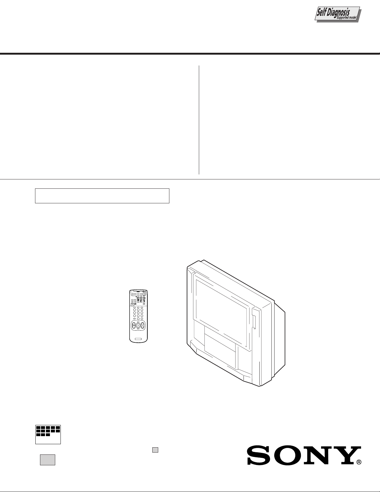
KWP-65HD1
KWP-65HD1
RM-Y904 US SCC-PO8A-A
RM-Y904
Canadian
SCC-PO8A-A
The service manual for SET TOP BOX(DTR-HD1)
have been issued separately (9-965-854-01)
MODEL COMMANDER DEST. CHASSIS NO.
–––––– –––––––––––– ––––– –––––––––––
POWER
SYSTEM
DVD/
DBS
MUTING
TV
OFF
VTR
CABLE
DVD/VTR
DBS/CABLE
TV
FUNCTION
OFF
FREEZE
AUDIO SWAP
POTITION
ZOOM IN
LEFT RIGHT
TV/DBS
GUIDE ACTIVE
CC
PICTURE
MODE
DISPLAY TV/VIDEO
ANT
3
1
2
6
4
5
9
7
8
ENTER
JUMP
0
MENU
VOL CH
RESET
TV
MICROFILM
∗ Please file according to model size........
65
HDTV Projection TV
Page 2

SPECIFICATIONS
Projection system 3 picture tubes, 3 lenses,
horizontal in-line system
Picture tube 7-inch high-brightness
monochrome tubes (6.3 raster
size), with optical coupling and
liquid cooling system
Projection lenses High performance, large
diameter hybrid lens F1.05
Television system American TV standard
Channel coverage DTV:2-69
VHF: 2–13/UHF: 14 –69
CATV: 1 – 125
Antenna 75 ohm external
terminal for VHF/UHF
Screen size (measured diagonally)
65 inches
Inputs/outputs on the upper panel
VIDEO 1/3 IN
VIDEO 2 INPUT
S VIDEO IN (4-pin mini DIN):
Y: 1 Vp-p, 75-ohms
unbalanced, sync negative
C: 0.286 Vp-p (Burst signal),
75 ohms
VIDEO (phono jack):
1 Vp-p,75-ohms unbalanced,
sync negative
AUDIO (phono jacks):
500 mVrms (100% modulation),
Impedance: 47 kilohms
VIDEO 4 IN
S VIDEO IN (4-pin mini DIN):
Y: 1 Vp-p, 75-ohms
unbalanced, sync negative
C: 0.286 Vp-p (Burst signal),
75 ohms
VIDEO (phono jack):
1 Vp-p, 75-ohms unbalanced,
sync negative
AUDIO (phono jacks):
500 mVrms (100% modulation),
Impedance: 47 kilohms
Y: 1 Vp-p, 75 ohms, sync negative
PB: 0.7 Vp-p, 75 ohms
PR: 0.7 Vp-p, 75 ohms
VIDEO 5 (HD) IN : Maximum scaning
rate 1080i
Y: 1 Vp-p, 75-ohms, negative or
tri-level sync
PB: 0.7 Vp-p, 75 ohms
PR: 0.7 Vp-p, 75 ohms
or
G: 0.7 Vp-p
B: 0.7 Vp-p
R: 0.7 Vp-p
HD:0.5-5 Vp-p , 2.2kilohms
VD:0.6-5 Vp-p , 2.2kilohms
Note:The VIDEO 5 (HD) IN jack are not compatible
with a computers 5BNC (R/G/B/HD/VD)
video output connectors.
AUDIO (phono jacks):
500 mVrms (100% modulation),
Impedance: 47 kilohms
VIDEO(phono jack): 1 Vp-p,
SELECT OUT
75 ohms unbalanced, sync negative
AUDIO(phono jacks): 470mVrms
(100% modulation),
Impedance:47 kilohms
AUDIO (VAR) OUT (phono jacks):
950 mVrms (100% modulation)
AUDIO (FIX) OUT (phono jacks):
500 mVrms (100% modulation)
Inputs/outputs on the lower panel
VIDEO 1/2 IN
S VIDEO OUT(4-pin mini DIN):
Y: 1 Vp-p, 75-ohms
unbalanced, sync negative
C: 0.286 Vp-p (Burst signal),
75 ohms
VIDEO (phono jack):
1 Vp-p, 75-ohms unbalanced,
sync negative
AUDIO (phono jacks):
470 mVrms (100% modulation),
Impedance: 47 kilohms
VIDEO 3/4 IN
Analog RGB/Component (phono jack)
Y: 1 Vp-p, 75 ohms, sync negative
PB: 0.7 Vp-p, 75 ohms
PR: 0.7 Vp-p, 75 ohms
R/G/B: 0.7 Vp-p, 75 ohms
HD SYNC: 3 Vp-p, positive
VD SYNC: 3 Vp-p, positive
DOLBY DIGITAL OUT (OPTICAL)
(optical output connector):
-18 dBm, wave length: 660 nm
S-LINK minijacks
CONTROL S IN/OUT :minijacks
Speaker
Front (Tweeter): 70mm (2 )
Front(Super Tweeter): 30mm(11/4 )X2
Front (Woofer): 130mm (5 ) x 2
Front (Center): 100mm (4 ) x 2
Rear:70mm(23/4 )x4
Speaker output Front: 20 W x 2
Center: 20 W x 1
Rear: 10 W x 2
Power requirement 120 V AC, 60 Hz
Power consumption In use (Max.): 300 W
In standby: 1 W
Dimensions (W/H/D) 1,767 x 1,570 x 738 mm
(52 1/8 x 56 3/4 x 24 1/2 inches)
Mass 217 kg (428 lbs 6 oz)
Supplied accessories Remote control RM-Y904(1)
Batteries (2) size AA (R6)
Rear speakers (2)
Speaker cords (2)
Optional accessories Connecting cables
PK-G34, RK-74A, RKG-69HG, VMC-
10HG, VMC-720M, VMC-810S/820S,
YC-15V/30V, Optical digital canle
U/V mixer EAC-66
Design and specifications are subject to change without notice.
– 2 –
Page 3
SAFETY CHECK-OUT
Troouble Light
AC Outlet Box
Ohmmeter
Cold-water Pipe
Fig. B. Checking for earth ground.
( US model only )
KWP-65HD1
RM-Y904
After correcting the original service problem, perfom the follow-
ing safety checks before releasing the set to the customer:
l. Check the area of your repair for unsoldered or poorly-sol-
dered connections. Check the entire board surface for solder
splashes and bridges.
2. Check the interboard wiring to ensure that no wires are
“pinched” or contact high-wattage resistors.
3. Check that all control knobs, shields, covers, ground straps,
and mounting hardware have been replaced. Be absolutely
certain that you have replaced all the insulators.
4. Look for unauthorized replacement parts, particularly transistors, that were installed during a previous repair. Point them
out to the customer and recommend their replacement.
5. Look for parts which, through functioning, show obvious
signs of deterioration. Point them out to the customer and
recom mend their replacement.
6. Check the line cords for cracks and abrasion. Recommend
the replacement of any such line cord to the customer.
7. Check the condition of the monopole antenna (if any). Make
sure the end is not broken off, and has the plastic cap on it.
Point out the danger of impalement on a broken antenna to
the customer, and recommend the antenna’s replacement.
8. Check the B+ and HV to see they are at the values specified.
Make sure your instruments are accurate;be suspicious of
your HV meter if sets always have low HV.
9. Check the antenna temminals, metal trim, “metallized” knobs,
screws, and all other exposed metal parts for AC leakage.
Check leakage as described below.
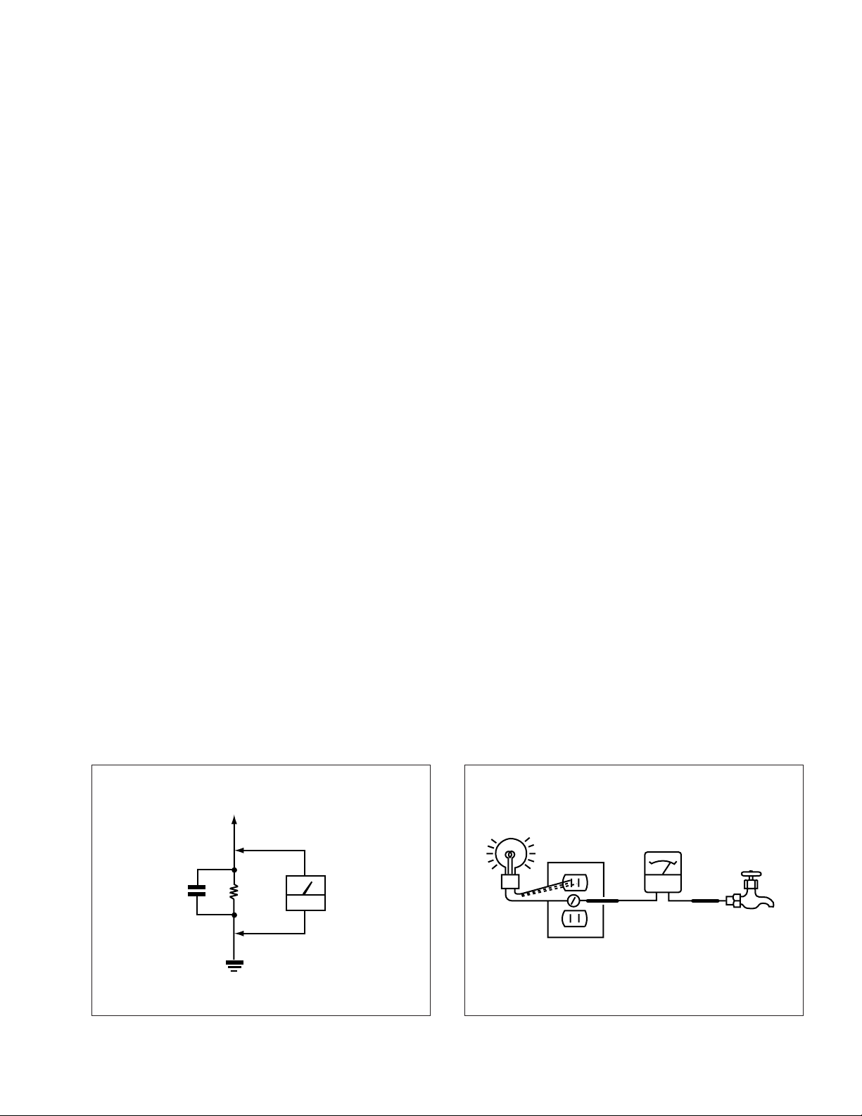
LEAKAGE TEST
The AC leakage from any exposed metal part to earth ground and
from all exposed metal parts to any exposed metal part having a
return to chassis, must not exceed 0.5mA (500 microampers) . Leakage current can be measured by any one of three methods.
1. A commercial leakage tester, such as the Simpson 229 or
RCA WT-540A. Follow the manufacturers’ instructions to
usc these instruments.
2. A battery-operated AC milliammeter . The Data Precision 245
digital multimeter is suitable for this job.
3. Measuring the voltage drop across a resistor by means of a
VOM or battery-operated AC voltmeter. The “limit” indication is 0.75V, so analog meters must have an accurate lowvoltage scale. The Simpson 250 and Sanwa SH-63Trd are
examples of a passive VOM that is suitable. NearIy all battery operated digital multimeters that have a 2V AC range
are suitable. (See Fig. A)
HOW TO FIND A GOOD EARTH GROUND
A cold-water pipe is guaranteed earth ground;the cover-plate retaining screw on most AC outlet boxes is also at earth ground. If
the retaining screw is to be used as your earth-ground, verify that it
is at ground by measuring the resistance between it and a coldwater pipe with an ohmmeter. The reading should be zero ohms. If
a cold-water pipe is not accessible, connect a 60-l00 watts trouble
light (not a neon lamp) between the hot side of the receptacle and
the retaining screw. Try both slots, if necessary, to locate the hot
side of the line, the lamp should light at normal brilliance if the
screw is at ground potential. (See Fig. B)
Fig. A. Using an AC voltmeter to check AC ieakage.
µ
F 1.5k
0.15
To Exposed Metal
Parts on Set
Ω
Earth Ground
AC
voltmeter
– 3 –
Page 4
KWP-65HD1
Lamp OFF :
3.0 seconds
Lamp ON : 0.3 seconds
Lamp OFF : 0.3 seconds
RM-Y904
SELF DIAGNOSIS FUNCTION
1. Summary of Self-Diagnosis Function
• This device includes a self-diagnosis function.
• In case of abnormalities, the Standby/Sleep lamp automatically blinks. It is possible to predict the abnormality location by the
number of blinks. The Instruction Manual describes blinking of the Standby/Sleep lamp.
• If the symptom is not reproduced sometimes in case of a malfunction, there is recording of whether a malfunction was generated or not. Operate the remote command to confirm the matter on the screen and to predict the location of the abnormality.
2. Diagnosis Items and Prediction of Malfunction Location
• When a malfunction occurs the Standby/Sleep lamp only blinks for one of the following diagnosis items. In case of two or
more malfunctions, the item which first occurred blinks. If the malfunctions occurred simultaneously, the item with the lower
blink count blinks first.
• The screen display displays the results regarding all the diagnosis items listed below. The display “ 0 ” means that no malfunctions occurred.
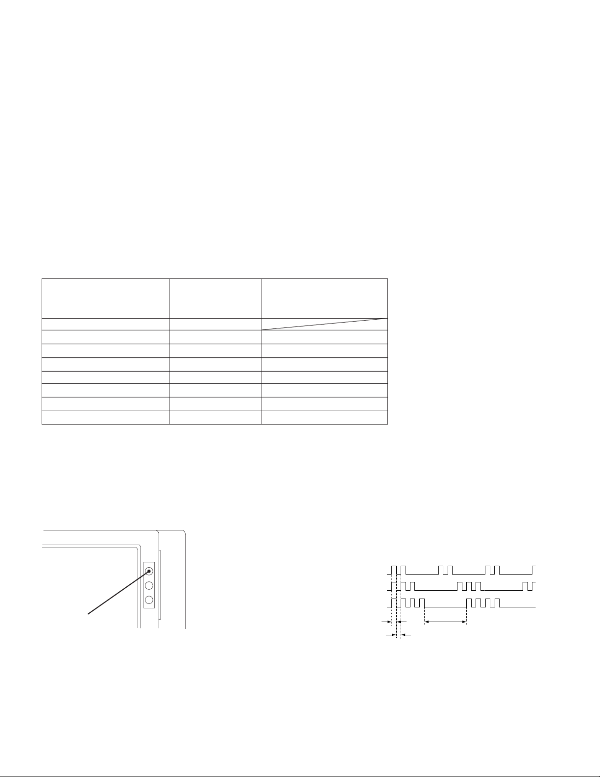
Diagnosis item Standby/ Self-diagnosis
sleep lamp, screen display,
Number of blinks Diagnosis item: Results
• Power not ON Not lit
+B OCP detection LED blinks 2 times 2 : +B OCP XX
+B OVP detection LED blinks 3 times 3 : +B OVP XX
V horizontal detection LED blinks 4 times 4 : V STOP XX
AKB detection LED blinks 5 times 5 : AKB XX
H vertical detection LED blinks 6 times 6 : H STOP XX
HV abnormality detection LED blinks 7 times 7 : HV XX
Audio abnormality detection LED blinks 8 times 8 : AUDIO XX
: XX the range of values for number of operations is 00-99. For 99 or higher there is no count up
*
and the number remains at 99.
3. Blinking count display of Standby/Sleep lamp
One blink is not used for self-diagnosis.
<
SCREEN FRAME
TIMER/STANDBY
indicator
Release of Standby/Sleep lamp blinking.
>
*
•EXAMPLE
<Diagnosis Items> <Number of Blinks>
• +B overcurrent 2 times
• +B overvoltage 3 times
• Vertical deflection stop 4 times
• The Standby/Sleep lamp blinking display is released by turning OFF the power switch on the TV main unit or removing the plug
from the power.
– 4 –
Page 5

KWP-65HD1
4. Self-diagnosis screen displays
• In cases of malfunctions where it is not possible to determine the symptom such as when the power goes off occasionally or when
the screen disappears occasionally, there is a screen display on whether the malfunction occurred or not in the past (and whether
the detection circuit operated or not) in order to allow confirmation.
<Screen Display Method>
• Quickly press the remote command button in the following order from the standby state.
RM-Y904
Display b Channel
b Volume – b Power ON
5
˘
Be aware that this differs from the method of
).
+
Self-diagnosis screen display
SELF CHECK
2 : +B OCP XX
3 : +B OVP XX
4 : V STOP XX
5 : AKB XX
6 : H STOP XX
7 : HV XX
8 : AUDIO XX
9 : WDT XX
entering the service mode (volume
÷
2 : +B OCP XX
Diagnosis
Results
XX the range of values for number of
operations is 00-99.
For 99 or higher there is no count up
and the numberremainsat 99.
5. Self-Diagnosis Screen Display
• The results display is not automatically cleared. In case of repairs and after repairs, check the self-diagnosis screen and be sure to
return the results display to “ 0 ”.
• If the results display is not returned to “ 0 ” it will not be possible to judge a new malfunction after completing repairs.
<Method of Clearing Results Display>
• When returning the results display to “ 0 ” (clear), press the remote command buttons in the following order when the diagnosis
screen is displayed.
• Be aware that, when carrying this out in the speed mode, all the other electrical adjustment data will be rewritten.
Channel 8 b ENTER
<Method of Ending Self Diagnosis Screen>
• When ending the self-diagnosis screen completely, turn the power switch OFF on the remote commander or the main unit.
– 5 –
Page 6

KWP-65HD1
RM-Y904
TABLE OF CONTENTS
Section Title Page
1. GENERAL
Remote Control ....................................................................... 7
Installing and Connecting the Projection TV .......................... 7
Basic Set Up .......................................................................... 16
Using Digital TV Feautres .................................................... 18
Using Conventional TV Features.......................................... 22
Operating Video Equipment.................................................. 40
Operating a Cable Box or DBS Receiver.............................. 41
Troubleshooting .................................................................... 42
2. DISASSEMBLY
2-1. Front Panel Removal .................................................. 44
2-2. HB Board Removal .................................................... 44
2-3. Screen Frame Assy and HC Board Removal.............. 44
2-4. HA Board and Control Panel Removal ...................... 44
2-5. Rear Board Removal .................................................. 45
2-6. Main Bracket Removal ............................................... 45
2-7. Service Position .......................................................... 45
2-8. UA, UB and Terminal Board Removal ...................... 45
2-9. BD, BR, BM and AW Boards Removal ..................... 46
2-10. G Board Removal ....................................................... 46
2-11. K Board Removal ....................................................... 46
2-12. Reflection Mirror Removal ........................................ 47
2-13. GA Board and STB(SET TOP BOX) Removal.......... 47
2-14. Picture Tube Removal ................................................ 48
2-12. High-Voltage Cable Installation and Removal........... 48
3. SET-UP ADJUSTMENTS............................................. 49
4. SAFETY RELATED ADJUSTMENTS..................... 64
5. CIRCUIT ADJUSTMENTS .......................................... 66
6. DIAGRAMS
6-1.Block diagram (1) .......................................................... 71
Block diagram (2) .......................................................... 74
Block diagram (3) .......................................................... 77
Block diagram (4) .......................................................... 80
Block diagram (5) .......................................................... 83
Block diagram (6) .......................................................... 86
Section Title Page
Block diagram (7) .......................................................... 89
Block diagram (8) .......................................................... 91
6-2.Frame Schematic Diagram ............................................. 93
6-3.Circuit Boards Location ................................................. 97
6-4.Printed Wiring Boards and Schematic Diagrams ........... 97
• A (1/4) Board ............................................................... 98
• A (2/4) Board ............................................................. 101
• A (4/4) Board ............................................................. 105
• A (3/4) Board ............................................................. 109
• BD Board ................................................................... 113
• BM Board .................................................................. 119
• BR (1/3) Board........................................................... 125
• BR (2/3) Board........................................................... 129
• BR (3/3) Board........................................................... 133
• G Board ...................................................................... 137
• K Board ...................................................................... 144
• D (1/2) Board ............................................................. 153
• D (2/2) Board ............................................................. 156
• UA Board ................................................................... 159
• UB Board ................................................................... 162
• A W Board................................................................... 165
• CR, CG Boards .......................................................... 168
• CB, ZR Boards........................................................... 171
• ZG, ZB Boards........................................................... 174
• HA, HB, HC Boards .................................................. 177
• GA,GB Boards........................................................... 179
6-5.Semiconductors ............................................................ 180
7. EXPLODED VIEWS
7-1.Cover (LOWER SECTION) ........................................ 183
7-2.Cover (UPPER SECTION) .......................................... 184
7-3.Chassis .......................................................................... 185
7-4.Picture Tube .................................................................
186
8. ELECTRICAL PARTS LIST...................................... 187
SHORT CIRCUIT THE ANODE OF THE PICTURE TUBE AND THE AN-
(CAUTION)
ODE CAP TO THE METAL CHASSIS, CRT SHIELD, OR CARBON PAINTED ON THE CRT, AFTER REMOVING THE ANODE.
WARNING!!
AN ISOLATION TRANSFORMER SHOULD BE USED DURING ANY SERVICE TO AVOID POSSIBLE SHOCK HAZARD, BECAUSE OF LIVE CHASSIS.
THE CHASSIS OF THIS RECElVER IS DIRECTLY CONNECTED TO THE
AC POWER LINE.
SAFETY-RELATED COMPONENT WARNING!!
COMPONENTS IDENTIFIED BY SHADING AND MARK ! ON THE SCHEMATIC DIAGRAMS, EXPLODED VIEWS AND IN THE PARTS LIST ARE
CRITICAL TO SAFE OPERATION. REPLACE THESECOMPONENTS WITH
SONY PARTS WHOSE PART NUMBERS APPEAR AS SHOWN IN THIS
MANUAL OR IN SUPPLEMENTS PUBLISHED BY SONY. CIRCUIT ADJUSTMENTS THAT ARE CRITICAL TO SAFEOPERATION ARE IDENTIFIED IN THIS MANUAL. FOLLOW THESE PROCEDURES WHENEVER
CRITICAL COMPONENTS ARE REPLACED OR IMPROPER OPERATION
IS SUSPECTED.
APRES AV OIR DECONNECTE LE CAP DE L’ANODE, COURTCIRCUITER
(ATTENTION)
L’ANODE DU TUBE CATHODIQUE ET CELUI DE L’ANODE DU CAP AU
CHASSIS METALLIQUE DE L’APPAREIL, OU AU COUCHE DE CARBONE
PEINTE SUR LE TUBE CATHODIQUE OU AU BLINDAGE DU TUBE
CATHODIQUE.
ATTENTION!!
AFIN D’EVITER TOUT RISQUE DELECTROCUTION PROVENANT D’UN
CHÁSSIS SOUS TENSION, UN TRANSFORMATEUR D’ISOLEMENT DOIT
ETRE UTILISÉ LORS DE TOUT DEPANNAGE.
LE CHÁSSIS DE CE RECEPTEUR EST DIRECTEMENT RACCORDÉ Á
L’ALIMENTATION SECTEUR.
ATTENTION AUX COMPOSANTS RELATIFS ÁLA
SÉCURITÉ!!
LES COMPOSANTS IDENTIFIÉS P AR UNE TRAME ET PAR UNE MAPQUE
! SUR LES SCHÉMAS DE PRINCIPE, LES VUES EXPLOSÉES ET LES
LISTES DE PIECES CONT D’UNEIMPORT ANCE CRITIQUE POUR LA SÉCURITÉ DU FONCTIONNEMENT . NE LES REMPLA CER QUE PAR DES COMPOSANTS SONY DONT LE NUMÉRO DE PIÉCE EST INDIQUÉ DANS LE
PRÉSENT MANUEL OU DANS DES SUPPLÉMENTS PUBLIÉS PAR SONY.
LES RÉGLAGES DE CIRCUIT DONT L’IMPORTANCE EST CRITIQUE
POUR LA SÉCURITÉ DU FONCTIONNEMENT SONT IDENTIFIES DANS
LE PRÉSENT MANUEL. SUIVRE CES PROCÉDURES LORS DE CHAQUE
REMPLACEMENT DE COMPOSANTS CRITIQUES, OU LORSQU’UN MAU-
VAIS FONCTIONNEMENT EST SUSPECTÉ.
– 6 –
Page 7
Remote Control
20°
min. 2.4m (approx. 8ft.)
20°
SECTION 1
GENERAL
The operating instructions mentioned here are partial abstracts from the
Operating Instructions Manual. The page numbers of the Operating
Instruction Manual remain as in the manual. (Par t no : 3-864-093-11)
In the instructions that follow, we will
refer to the buttons on your remote control.
Keep this flap unfolded and use this page
for reference.
MTS
(page 38)
VTR1/2/3/DVD/
MDP switch
(page 72)
PIP/P&P/
CHANNEL INDEX
(pages 40-44)
VCR/DVD/MDP
operation
buttons
(page 73)
CODE SET
(pages 72,74)
MUTING
SLEEP
VTR123DVD/MDP
AUDIO SWAP
TV/VIDEO DTV ANT
1
4
7
DVD/
VTR
DVD/VTRDBS/CABLE
(pages 29,37)
PIP/P&P/CHANNEL
INDEX
WIDE MODE
(pages 30,39)
CC
(pages 29,38)
PICTURE MODE
JUMP
POWER
DBS/
TV
CABLE
FUNCTION
TV
MTS
FREEZEPOSITION
DVD MENU
REC
TITLECODE SET
TV ANT
3
2
6
5
9
8
POWER
(pages
TV
TV
28,36,73)
FUNCTION
(pages
28,36,72,74)
ALTERNATE
(VIDEO/
AUDIO)
GUIDE
(page 31)
DISPLAY
(pages 29,37)
TV ANT
(page 36)
DTV ANT
(pages 25,28)
0–9 buttons
(pages 28,36)
ENTER
28,36,70)
CH +/–
(pages 28,36)
Joystick
(page 23)
MUTING
POWER
DVD/
MUTING
(pages 40–44)
TV/DBS/
(page 47)
FUNCTION
OFF
WIDE MODE
TV/DBS
PICTURE
MODE
(pages 28,37)
TV/VIDEO
(pages
29,38)
• (dot)
button
(page 28)
MENU
(pages
32,46)
VOL +/–
(pages
28,36)
RESET
(page 47)
*Note:
• The ALTERNATE (VIDEO/AUDIO) buttons do not
function with this projection TV. When digital TV
programs which are compatible with these buttons begin
broadcasting in the near future, consult your nearest Sony
dealer or Sony Direct Response Center.
DBS/
SLEEP
VTR
CABLE
DVD/VTR
DBS/CABLE
CC
DISPLAY
ALTERNATE
VIDEO AUDIO
JUMP GUIDE
TV/VIDEO DTV ANT
TV ANT
1
2
4
5
7
8
ENTER
0
MENU
VOL CH
RESET
HDTV
3
6
9
Getting to know the buttons on the
remote control
Names of the buttons on the remote control are
presented in different colors to represent the
available functions.
Button color
*
Transparent .... Press to select the component
Green ............... Buttons relevant to power
Label color
(pages
White ............... TV/VTR (VCR)/MDP/DVD
Yellow .............. PIP, P&P, and CHANNEL
Blue .................. DBS operation buttons
Pink .................. DVD Player operation buttons
For a detailed explanation of most buttons, see
“Watching Digital TV” on page 28, or
“Watching Conventional TV” on page 36.
you want to control; e.g. VTR
(VCR)/MDP/DVD Player,
DBS (Direct Broadcast
Satellite)/CABLE, or projection
TV.
operations, like turning the
projection TV, DBS/CABLE, or
VTR (VCR)/MDP/DVD Player
on or off
Player/DBS (Direct Broadcast
Satellite)/CABLE operation
buttons
INDEX operation buttons
Carrying Your Projection TV
Carrying the projection TV requires four or
more people.
The projection TV has been equipped with
casters for easy movement on a hard surface.
Please move your projection TV using the
casters.
Installing and Connecting the Projection TV
Installing the Projection TV
Recommended viewing area
(Horizontal)
min. 2.4m (approx. 8 ft.)
60°
60°
60°
Recommended viewing area
(Vertical)
5
– 7 –
Page 8
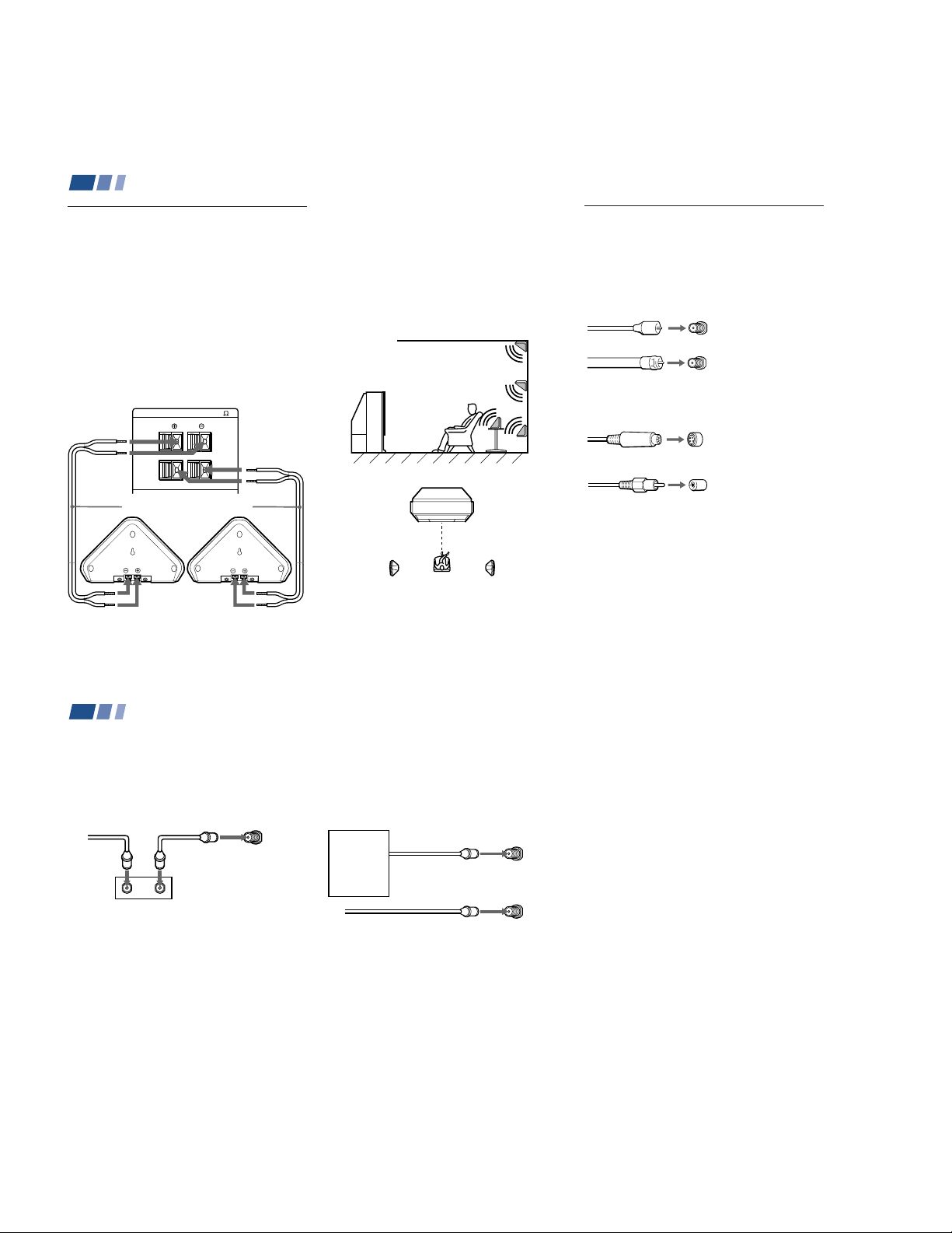
Installing and Connecting the Projection TV (continued)
Mounting the Supplied Rear
Speakers
For enhanced surround effect, connect the
supplied rear speakers to your projection TV.
Connecting the rear speakers
Using the supplied speaker cords, connect
REAR SPEAKER OUT L on your projection
TV to the speaker terminal on one rear
speaker, and connect REAR SPEAKER OUT
R to the terminal on the other one.
Speaker (supplied)
6
(Rear of projection TV)
REAR SPEAKER OUT(MIN 16
Speaker cord (supplied)
)
L
R
Speaker (supplied)
Installation
For optimum surround effect, mount the rear
speakers in the following places (as shown in
the illustration):
• on a wall, a little higher or lower than the
listener’s ears.
• on a table, a little lower than the listener’s
ears.
• at the corner where the wall and ceiling
meet.
Projection TV
(Rear of projection TV)
Left rear
speaker
Note:
• Match the colors of the speaker cords and
the terminals. If the colors are reversed,
sound will be distorted.
Rear speaker
Right rear
speaker
Connector Types
You may find it necessary to use some of the
following connector types during set up.
Coaxial cable
Standard TV cable and antenna cable
Plug Type
Push into connection.
Screw-on Type
Screw into connection.
S Video cable
High quality video cable for enhanced
picture quality
Audio/Video cable
Video - Yellow
Audio (Left) - White
Audio (Right) - Red
Some DVD Players are equipped with the
following three video connectors.
Y - Green
P
B (CB, Cb or B–Y) - Blue
P
R (CR, Cr or R–Y) - Red
Align guides and
push into connection.
Push into connection.
Installing and Connecting the Projection TV (continued)
Connecting a cable box
Some pay cable TV systems use scrambled or
encoded signals that require a cable box* to
view all channels.
(Rear of projection TV)
Cable
IN
*Cable box
OUT
Note:
• If you will be controlling all channel
selection through your cable box, you
should consider using the CHANNEL
FIX feature. (see “CHANNEL FIX” on
page 56)
8
VHF/UHF
Cable box and cable
Some pay cable TV systems use scrambled or
encoded signals requiring a cable box* only for
certain channels (e.g. HBO, SHOWTIME, etc.)
*Cable box
CATV cable
(unscrambled channels)
For this set up, you can switch between
scrambled channels (through your cable
box), and normal (CATV) channels by
pressing TV ANT on your remote control.
Notes:
• You may be able to program your Sony
remote control to operate your cable box.
(see “Operating a Cable Box or DBS
Receiver” on page 74)
• During PIP, P&P, CHANNEL INDEX or
FAVORITE CHANNEL viewing, the
AUX input can only be viewed in the
main picture.
(Rear of projection TV)
AUX
VHF/UHF
• If you are connecting a cable box through
the AUX input and would like to switch
between the AUX and normal (CATV)
input, you should consider using
CHANNEL FIX.
(see “CHANNEL FIX” on page 56)
– 8 –
Page 9
CONTROL SCONTROL S
DOLBY DIGITALDOLBY DIGITAL
OUT
(OPTICALL)
IN
OUT
SD/HD
S VIDEO
S-LINK/
CONTROL S
OUT
S-LINK/
CONTROL S
IN
VIDEO
AUDIO
L
R
R
VIDEO
L
AUDIO
VHF/UHF
AUX
(MONO)
IN OUT
VIDEO 1 VIDEO 3 VIDEO 4 (DVD) SELECT
VHF/UHF
(DIGITAL)
Y
P
B
PR
LINE
OUT
OUT
IN
AUDIO R AUDIO L VIDEO
S VIDEO
VHF/UHF
LINE
IN
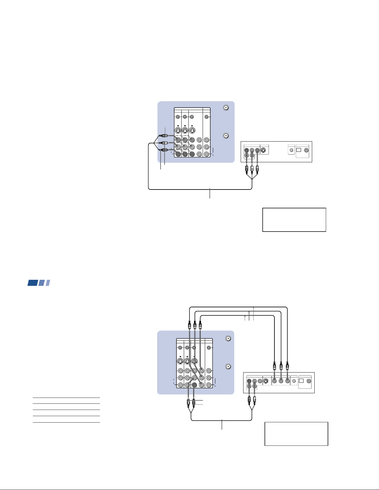
Connecting an antenna/cable TV
system to a VCR
1 Attach the coaxial cable from the roof
antenna to VHF/UHF (DIGITAL) on the
TV’s lower panel.
2 Attach the coaxial cable from the
incoming cable connection or antenna to
IN on the VCR.
3 Using a coaxial cable, connect OUT on the
VCR to VHF/UHF on the TV’s upper
panel.
4 Using AUDIO and S VIDEO* cables,
connect AUDIO and S VIDEO OUT on the
VCR to AUDIO and S VIDEO IN on the
TV’s upper panel (White-AUDIO Left,
Red-AUDIO Right).
* If your VCR is not equipped with S VIDEO, use a
VIDEO cable (yellow) instead of the S VIDEO
cable.
Note:
• If you are connecting a monaural VCR,
connect only the single audio output to
the left (MONO) input on the projection
TV.
S VIDEO
Roof
antenna
(Rear of projection TV)
1
Disconnect all power sources before making any connections.
3
Coaxial cable
VIDEO
AUDIO-L
AUDIO-R
VCR
2
Cable/
Antenna
RK-74A (not supplied)
4
YC-15V/30V (not supplied)
9
Installing and Connecting the Projection TV (continued)
Connecting a VCR and projection
TV to a cable box
1 Attach the coaxial cable from the roof
antenna to VHF/UHF (DIGITAL) on the
TV’s lower panel.
2 Connect the single (input) jack of the
splitter to the incoming cable connection,
and connect the other two (output) jacks
(using the coaxial cable) to IN on the cable
box and VHF/UHF on the TV’s upper
panel.
3 Using a coaxial cable, connect OUT on the
cable box to IN on the VCR.
4 Using AUDIO and S VIDEO* cables,
connect AUDIO and S VIDEO OUT on the
VCR to AUDIO and S VIDEO IN on the
TV’s upper panel (White-AUDIO Left,
Red-AUDIO Right).
* If your VCR is not equipped with S VIDEO, use a
VIDEO cable (yellow) instead of the S VIDEO
cable.
Note:
• To view scrambled channels through the
cable box, select the video input which the
cable box is connected to by pressing TV/
VIDEO.
10
S VIDEO
VHF/UHF
(DIGITAL)
CONTROL SCONTROL S
1
Roof
antenna
(Rear of projection TV)
VIDEO 1 VIDEO 3 VIDEO 4 (DVD) SELECT
S-LINK/
CONTROL S
OUT
S VIDEO
VIDEO
L
(MONO)
AUDIO
R
DOLBY DIGITAL
OUT
IN
(OPTICALL)
SD/HD
OUT
Disconnect all power sources before making any connections.
IN OUT
VIDEO
AUDIO-L
AUDIO-R
RK-74A (not supplied)
AUX
S-LINK/
CONTROL S
IN
VHF/UHF
Y
VIDEO
P
B
L
P
R
R
AUDIO
Coaxial cable
VCR
AUDIO R AUDIO L VIDEO
LINE
IN
LINE
OUT
S VIDEO
VHF/UHF
OUT
IN
4
Cable box
3
OUT
IN
2
YC-15V/30V (not supplied)
2
Splitter
(not supplied)
Cable/
Antenna
– 9 –
Page 10
S VIDEO
S-LINK/
CONTROL S
OUT
S-LINK/
CONTROL S
IN
VIDEO
AUDIO
L
R
VIDEO
(MONO)
IN OUT
VIDEO 1 VIDEO 3 VIDEO 4 (DVD) SELECT
Y
P
B
P
R
R
L
AUDIO
VHF/UHF
AUX
VHF/UHF
S VIDEO
OUT
IN
LINE OUT
SATELLITE IN
AUDIO R AUDIO L VIDEO
(DIGITAL)
VHF/UHF
Connecting a DBS (Direct
CONTROL S
DOLBY DIGITAL
OUT
(OPTICALL)
IN
OUT
SD/HD
S VIDEO
S-LINK/
CONTROL S
OUT
S-LINK/
CONTROL S
IN
VIDEO
AUDIO
L
R
VIDEO
(MONO)
IN OUT
VIDEO 1 VIDEO 3 VIDEO 4 (DVD) SELECT
Y
P
B
P
R
LINE
OUT
OUT
IN
AUDIO R AUDIO L VIDEO
S VIDEO
VHF/UHF
LINE
IN
LINE
OUT
OUT
IN
VHF/UHF
SATELLITE IN
R
L
AUDIO
VHF/UHF
AUX
VHF/UHF
(DIGITAL)
Broadcast Satellite) receiver
1 Attach the coaxial cable from the roof
antenna to VHF/UHF (DIGITAL) on the
TV’s lower panel.
2 Connect the cable from the satellite
antenna to the DBS receiver.
3 Attach the coaxial cable from the incoming
cable connection or antenna to VHF/UHF
on the TV’s upper panel.
4 Using AUDIO and S VIDEO cables,
connect AUDIO and S VIDEO OUT on the
DBS receiver to AUDIO and S VIDEO IN
on the TV’s upper panel (White-AUDIO
Left, Red-AUDIO Right).
Note:
• To view input from the DBS, select the
video input which the DBS receiver is
connected to by pressing TV/VIDEO on
the remote control.
(Rear of projection TV)
Roof
antenna
1
Disconnect all power sources before making any connections.
S VIDEO
AUDIO-L
AUDIO-R
RK-74A (not supplied)
Cable/
Antenna
Satellite antenna
cable
2
3
DBS
4
YC-15V/30V (not supplied)
11
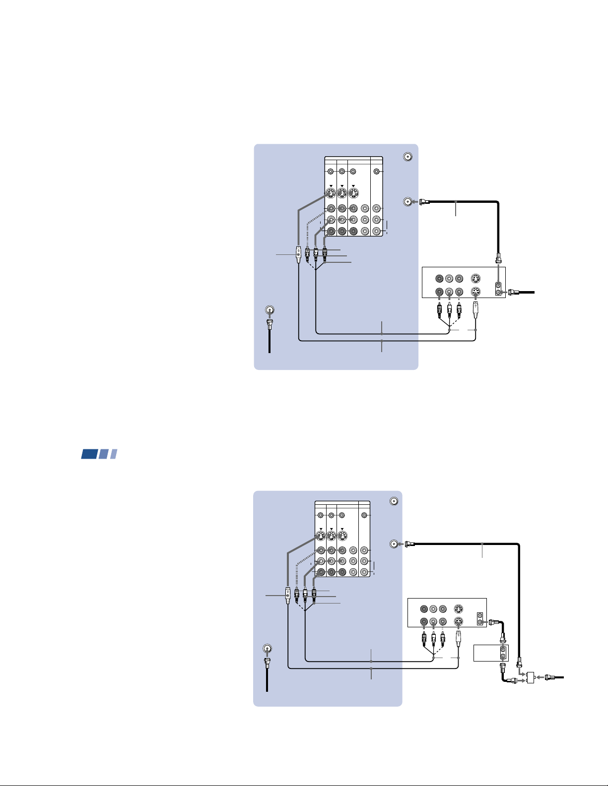
Installing and Connecting the Projection TV (continued)
Connecting a DBS (Direct
Broadcast Satellite) receiver and a
VCR
1-2 Perform as described on page 11.
3 Attach the coaxial cable from the
incoming cable connection or antenna to
IN on the VCR.
4 Using a coaxial cable, connect OUT on the
VCR to VHF/UHF on the TV’s upper
panel.
5 Using AUDIO and S VIDEO cables,
connect AUDIO and S VIDEO OUT on the
DBS receiver to AUDIO and S VIDEO IN
on the VCR.
6 Using AUDIO and S VIDEO* cables,
connect AUDIO and S VIDEO OUT on the
VCR to AUDIO and S VIDEO IN on the
TV’s upper panel (White-AUDIO Left,
Red-AUDIO Right).
* If your VCR is not equipped with S VIDEO, use a
VIDEO cable (yellow) instead of the S VIDEO
cable.
Note:
• To view input from the DBS or VCR,
select the video input which your DBS
receiver or VCR is connected to by
pressing TV/VIDEO on the remote
control.
12
S VIDEO
1
Roof
antenna
(Rear of projection TV)
6
YC-15V/30V (not supplied)
– 10 –
Disconnect all power sources before making any connections.
Coaxial cable
4
DBS
2
Satellite
antenna
cable
AUDIO-L
AUDIO-R
RK-74A (not supplied)
VMC-810S/820S
(not supplied)
5
VCR
3
Cable/
Antenna
Page 11
Connecting a camcorder
Use this connection to view a picture directly
from your camcorder.
1 Using an AUDIO/VIDEO cable, connect
AUDIO and VIDEO OUT on the
camcorder to AUDIO and VIDEO IN on
the lower left side on the front of the
projection TV (Yellow-VIDEO, WhiteAUDIO Left, Red-AUDIO Right).
2 Press VIDEO 2 to select the video inputs
from a camcorder.
Notes:
• If you are connecting a monaural
camcorder, connect only the single audio
output to the left (MONO) input on the
projection TV.
• If you have an S Video equipped
camcorder, you can use an S Video
connection.
Disconnect all power sources before making any connections.
(Front of projection TV)
PUSH
2
VIDEO 2
S VIDEO
L(MONO)
VIDEO
VIDEO
AUDIO-L
R
AUDIO
AUDIO-R
VMC-810S/820S
(not supplied)
Audio/video
outputs
1
Camcorder
13
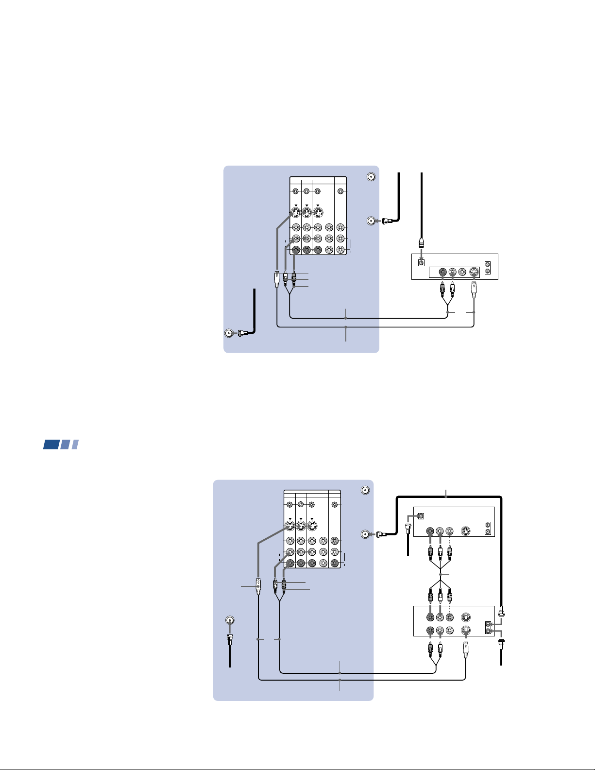
Installing and Connecting the Projection TV (continued)
Connecting two VCRs for tape
editing
SELECT OUT gives you the ability to use a
second VCR to record a program being
played by the primary VCR or to perform
tape editing and dubbing.
1 Connect the VCR intended for playback
using the connection instructions on page
9 of this manual.
2 Using an AUDIO/VIDEO cable, connect
AUDIO and VIDEO IN on the VCR
intended for recording to AUDIO and
VIDEO OUT of SELECT OUT on the TV’s
upper panel.
Notes:
• Do not change the input signal while
editing through SELECT OUT.
• When connecting a single VCR to the
projection TV: if VCR LINE OUT is
connected to VIDEO IN on the TV’s
upper panel, do not connect the SELECT
OUT on the TV’s upper panel to the VCR
LINE INPUT (see right). Doing so will
cause program interference and other
viewing problems.
• You can select the output signal from
SELECT OUT from the SET UP menu.
(see “SELECT OUT” on page 60)
14
VCR
(for playback)
1
VMC-810S/820S
(not supplied)
AUDIO R AUDIO L VIDEO
Disconnect all power sources before making any connections.
(Rear of projection TV)
AUX
S-LINK/
CONTROL S
IN
VHF/UHF
VIDEO
B
L
R
R
AUDIO
VCR (for recording)
AUDIO R AUDIO L VIDEO
OUT
LINE
IN
IN
LINE
OUT
S-LINK/
CONTROL S
OUT
VIDEO
S VIDEO
VIDEO
AUDIO
AUDIO-L
AUDIO-R
OUT
IN
(MONO)
IN OUT
VIDEO 1 VIDEO 3 VIDEO 4 (DVD) SELECT
Y
L
R
P
P
VIDEO
AUDIO-L
AUDIO-R
2
(Rear of projectionTV)
VIDEO IN
SELECT
OUT
VCR
IN
LINE
VMC-810S/820S (not supplied)
Indicates direction
of signal
OUT
– 11 –
Page 12
LINE OUT
S VIDEO OUT
S-LINK
DIGITAL OUT
R–AUDIO 1–L VIDEO
OPTICAL COAXIAL
S VIDEO
S-LINK/
CONTROL S
OUT
S-LINK/
CONTROL S
IN
VIDEO
AUDIO
L
R
VIDEO
(MONO)
IN OUT
VIDEO 1 VIDEO 3 VIDEO 4 (DVD) SELECT
Y
P
B
PR
R
L
AUDIO
VHF/UHF
AUX
Connecting a DVD Player without
component video output
connectors
Using an AUDIO/VIDEO cable, connect
AUDIO and VIDEO IN on the TV’s upper
panel to LINE OUT on the DVD Player
(White-AUDIO Left, Red-AUDIO Right).
Disconnect all power sources before making any connections.
(Rear of projection TV)
VIDEO
Note:
• Since the high quality pictures on a DVD
disc contain a lot of information, picture
noise may appear. In this case, adjust NR
in the VIDEO menu. (see “NR” on page
48)
Installing and Connecting the Projection TV (continued)
Connecting a DVD Player with
component video output
connectors
1 Using an AUDIO cable, connect AUDIO R
and L of LINE OUT on the DVD Player to
AUDIO R and L of VIDEO 4 IN on the TV’s
upper panel (White-AUDIO Left, Red
AUDIO Right).
2 Using three yellow VIDEO cables,
connect Y, P
COMPONENT VIDEO OUT on the DVD
Player to Y, P
the TV’s upper panel.
Notes:
• Some DVD Player terminals may be
labeled differently. If so, connect as
follows:
Connect To
Y (green) Y
PB (blue) CB, Cb or B-Y
PR (red) CR, Cr or R-Y
• Since the high quality pictures on a DVD
disc contain a lot of information, picture
noise may appear. In this case, adjust NR
in the VIDEO menu. (see “NR” on page
48)
16
B, and PR of the
B, and PR of VIDEO 4 IN on
AUDIO-L
AUDIO-R
(Rear of projection TV)
S-LINK/
CONTROL S
OUT
S VIDEO
VIDEO
L
(MONO)
AUDIO
R
DVD
Audio/video
outputs
VMC-810S/820S (not supplied)
Connect the DVD Player directly to
the projection TV. Connecting the
DVD Player through other video
equipment will cause unwanted
picture noise.
Disconnect all power sources before making any connections.
VMC-10HG (not supplied)
Y
P
B
P
R
S-LINK/
CONTROL S
VIDEO
L
R
AUDIO
AUDIO-L
AUDIO-R
AUX
IN
VHF/UHF
LINE OUT
R–AUDIO 1–L VIDEO
2
S VIDEO OUT
COMPONENT VIDEO OUT
R-YY B-Y
S-LINK
IN OUT
VIDEO 1 VIDEO 3 VIDEO 4 (DVD) SELECT
1
Connect the DVD Player directly
RK-74A (not supplied)
to the projection TV. Connecting
the DVD Player through other
video equipment will cause
unwanted picture noise.
DVD
DIGITAL OUT
OPTICAL COAXIAL
15
– 12 –
Page 13
S VIDEO
S-LINK/
CONTROL S
OUT
S-LINK/
CONTROL S
IN
VIDEO
AUDIO
L
R
R
VIDEO
L
(MONO)
IN OUT
VIDEO 1 VIDEO 3 VIDEO 4 (DVD) SELECT
Y
P
B
PR
LINE
OUT
OUT
IN
LINE
IN
VHF/UHF
AUDIO
VHF/UHF
AUX
VHF/UHF
(DIGITAL)
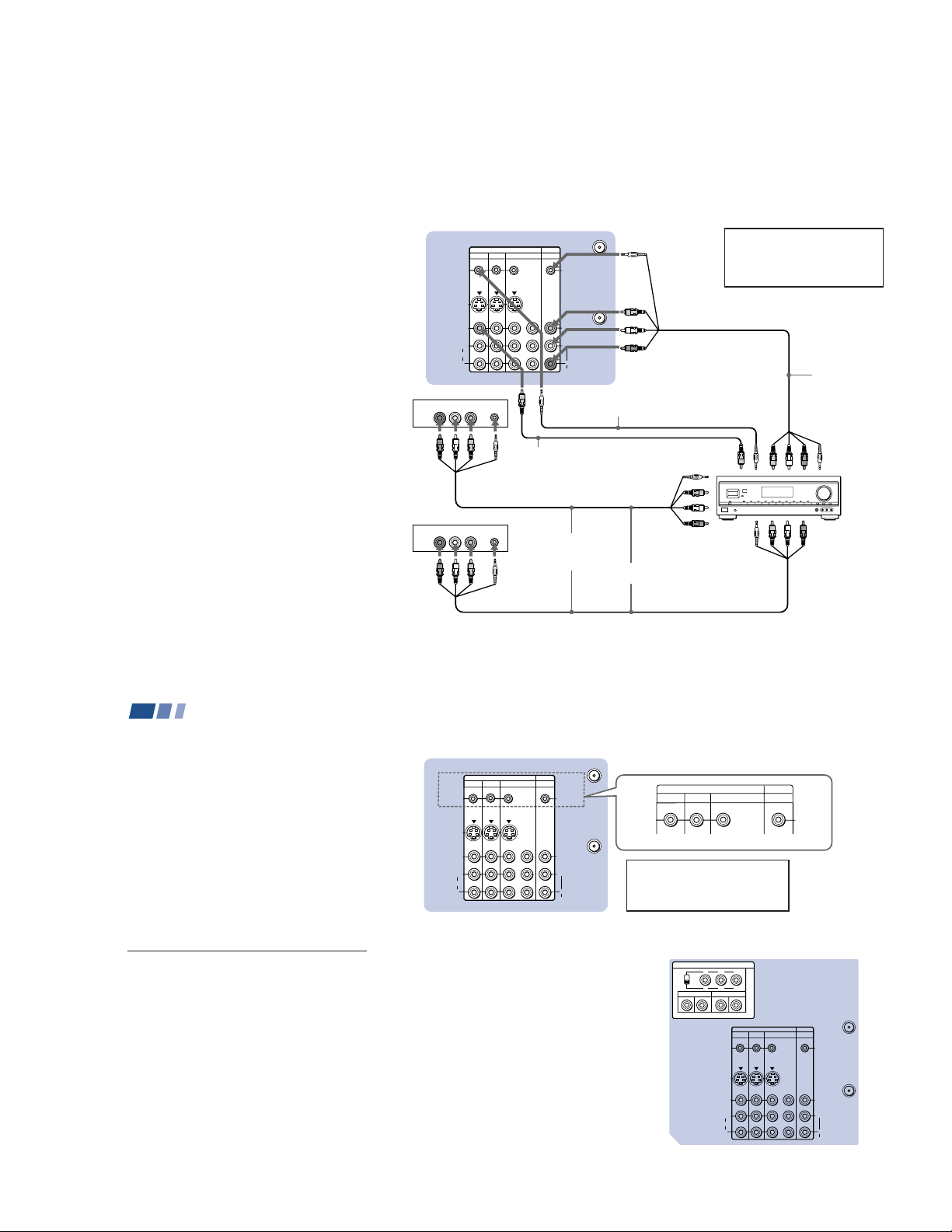
Connecting an AV receiver
For greater control of all audio and video
equipment, connect an AV receiver.
1-3 Perform as described on page 9.
4 Using a VIDEO cable, connect VIDEO 1 IN
on the TV’s upper panel to MONITOR
OUT on the AV receiver.
5 Using an AUDIO/VIDEO cable, connect
SELECT OUT on the TV’s upper panel to
VIDEO 2 IN on the AV receiver.
6 Using an AUDIO/VIDEO cable, connect
the video equipment to the AV receiver.
7 Use the SET UP menu to set SELECT OUT to
TV OUT. (see “SELECT OUT” on page 60)
Note:
• You may want to use CHANNEL FIX to
fix your TV’s input to the AV receiver
(VIDEO 1). (see “CHANNEL FIX” on
page 56)
Roof
Antenna
1
(Rear of projection TV)
VIDEO
Disconnect all power sources before making any connections.
Coaxial cable
3
VMC-810S/820S (not supplied)
6
VCR
5
VMC-10HG
4
VIDEO
AUDIO-L
AUDIO-R
VMC-810S/
820S (not
supplied)
MONITOR
OUT
AUDIO/
VIDEO
2 IN
VMC-810S/
820S (not
supplied)
6
2
Cable/
Antenna
AUDIO/
VIDEO 1 IN
Installing and Connecting the Projection TV (continued)
Connecting an audio system
For more dynamic sound, connect an audio
system to the projection TV.
1 Using an AUDIO cable, connect AUDIO
(VAR) OUT on the TV’s upper panel to
one of the unused Line inputs (e.g. Tape2, AUX1, etc.) on the stereo (WhiteAUDIO Left, Red-AUDIO Right).
2 Set the stereo to the chosen Line input
and use the AUDIO menu to switch the
TV’s speakers off. (see “SPEAKER” on
page 49)
Note:
• You can adjust VOLUME, BASS, TREBLE
and BALANCE through the projection
TV on AUDIO (VAR) OUT only.
AV receiver
AUDIO/
VIDEO 1
OUT
17
Disconnect all power sources before making any connections.
(Rear of projection TV)
L
R
AUDIO OUT
VAR FIX
AUDIO (VAR) OUT-L
L
R
AUDIO (VAR)
OUT-R
1
RK-74A
(not supplied)
Line input
2
HRD
Stereo amplifier
18
– 13 –
Page 14
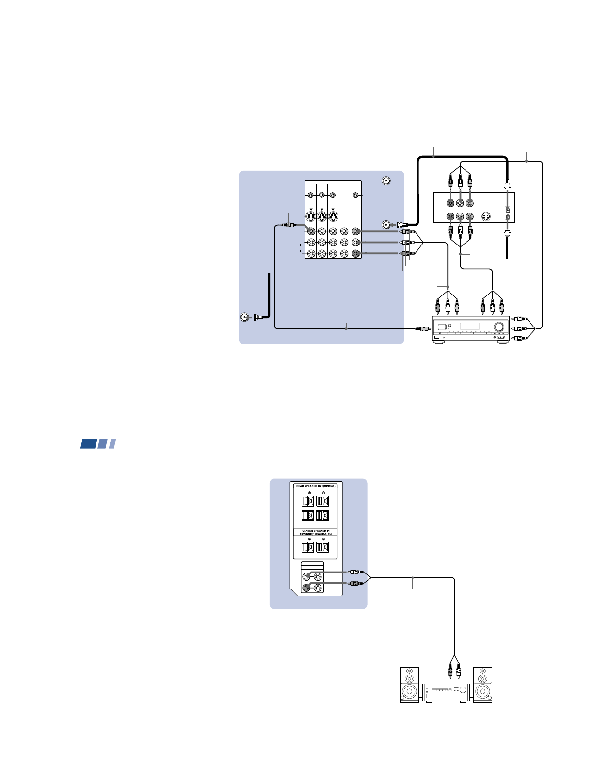
Connecting an amplifier that
supports Dolby Pro Logic/Dolby
Digital decoder
If you use an amplifier with a Dolby Pro
Logic/Dolby Digital decoder instead of the
projection TV’s audio system, you can still
use the projection TV’s center speaker.
1 Using the speaker cords (supplied with
the amplifier), connect the speaker
terminals on the amplifier to CENTER
SPEAKER IN +/– on the TV’s upper
panel.
2 Using an AUDIO cable, connect AUDIO
(FIX) OUT on the TV’s upper panel to one
of the unused Line inputs (e.g. Tape-2,
AUX1, etc.) on the amplifier (WhiteAUDIO Left, red-AUDIO Right).
3 If the amplifier is equipped with a digital
audio input, connect DOLBY DIGITAL
OUT (OPTICAL) on the TV’s lower panel
to the digital audio input on the amplifier
using the optical digital cable.
4 Set the amplifier to the chosen Line input
and use the AUDIO menu to set
“SPEAKER” to “CENTER IN” on the
projection TV. (see “SPEAKER” on page
49)
Note:
• The Dolby Pro Logic/Dolby Digital
decoder’s digital audio input jacks are
sometimes labeled AC-3 or DCN.
VIDEO
DOLBY DIGITAL
OUT
(OPTICALL)
Disconnect all power sources before making any connections.
(Rear of projection TV)
L
R
CENTER IN ’
AUDIO OUT
FIX
VAR
L
R
AUDIO (FIX) OUT-R
RK-74A (not supplied)
Digital
3
audio input
Rear
speaker (L)
S VIDEO
OUT
VIDEO
1 2
L
(MONO)
R
1
AUDIO OUT
VIDEO OUT
4
3
R
Y
GBHD
P
B
2
VD
PR
Optical digital cable
CENTER IN ‘
AUDIO (FIX) OUT-L
2
Line input
Amplifier with Dolby
Pro Logic/Dolby Digital
decoder
Front
speaker (L)
Woofer
4
speaker (R)
Front
speaker (R)
1
Rear
19
Installing and Connecting the Projection TV (continued)
Using the S-Link/CONTROL S
Function
S-Link is a Sony innovation designed to
make the Sony components work together. It
allows you to automatically switch the
projection TV’s input mode to video when
you press the play button on the Sony S-Link
VCR.
Using the S-Link function without
a Sony AV receiver
1 Connect the Sony VCR (DVD). (see
“Connecting an antenna/cable TV system
to a VCR” on page 9 or “Connecting a
DVD Player with component video
output connectors” on page 16)
2 Using an S-LINK cable, connect the
S-LINK jacks on the VCR (DVD) and the
TV’s upper panel. Ensure that both ends
are seated firmly and that the projection
TV’s S-LINK jack is in the same row as
the AUDIO/VIDEO cable extending from
the Sony VCR (DVD).
20
Refer also to the Operating
Instructions supplied with
the VCR, DBS tuner, DVD
player, LD player and other
Sony video equipment for
details.
(Rear of projection TV)
IN OUT
VIDEO 1 VIDEO 3 VIDEO 4 (DVD) SELECT
S-LINK/
CONTROL S
OUT
S VIDEO
VIDEO
L
(MONO)
AUDIO
R
Y
P
PR
VIDEO
AUDIO-L
AUDIO-R
S-LINK
Disconnect all power sources before making any connections.
RK-G34, etc. (not supplied)
Sony DVD
LINE OUT
S VIDEO OUT
R–AUDIO 1–L VIDEO
S-LINK
VIDEO5
AUX
S-LINK/
CONTROL S
IN
RK-74A (not supplied)
VHF/UHF
VIDEO
B
L
R
AUDIO
Audio/video/S-LINK cable
COMPONENT VIDEO OUT
Audio
outputs
Audio/video
outputs
AUDIO R AUDIO L VIDEO
LINE
OUT
S-LINK
PRYPB
Component
video
outputs
Sony VCR
S-LINK
DIGITAL OUT
OPTICAL COAXIAL
VMC-10HG
(not
supplied)
S-LINK
S-LINK
– 14 –
Page 15
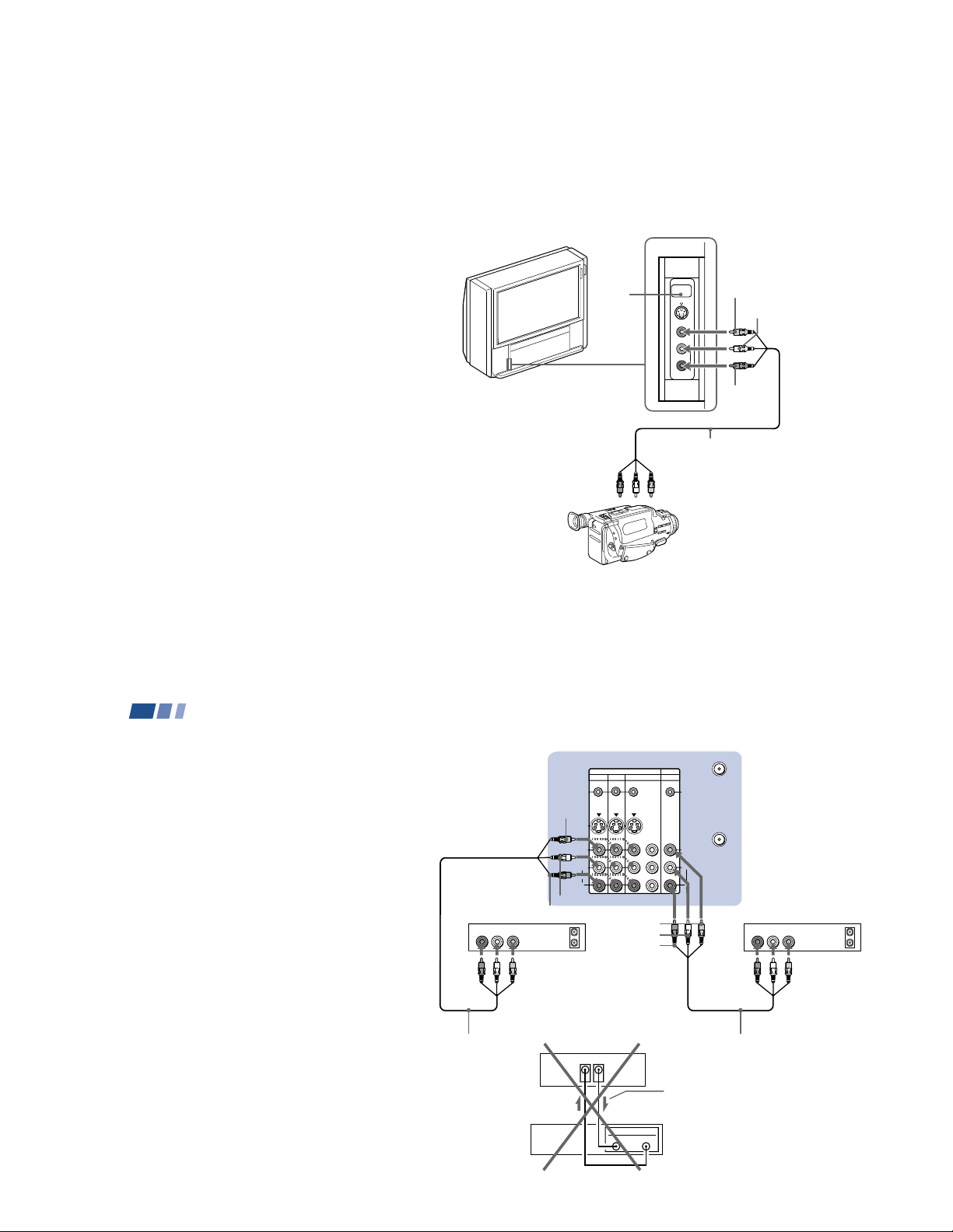
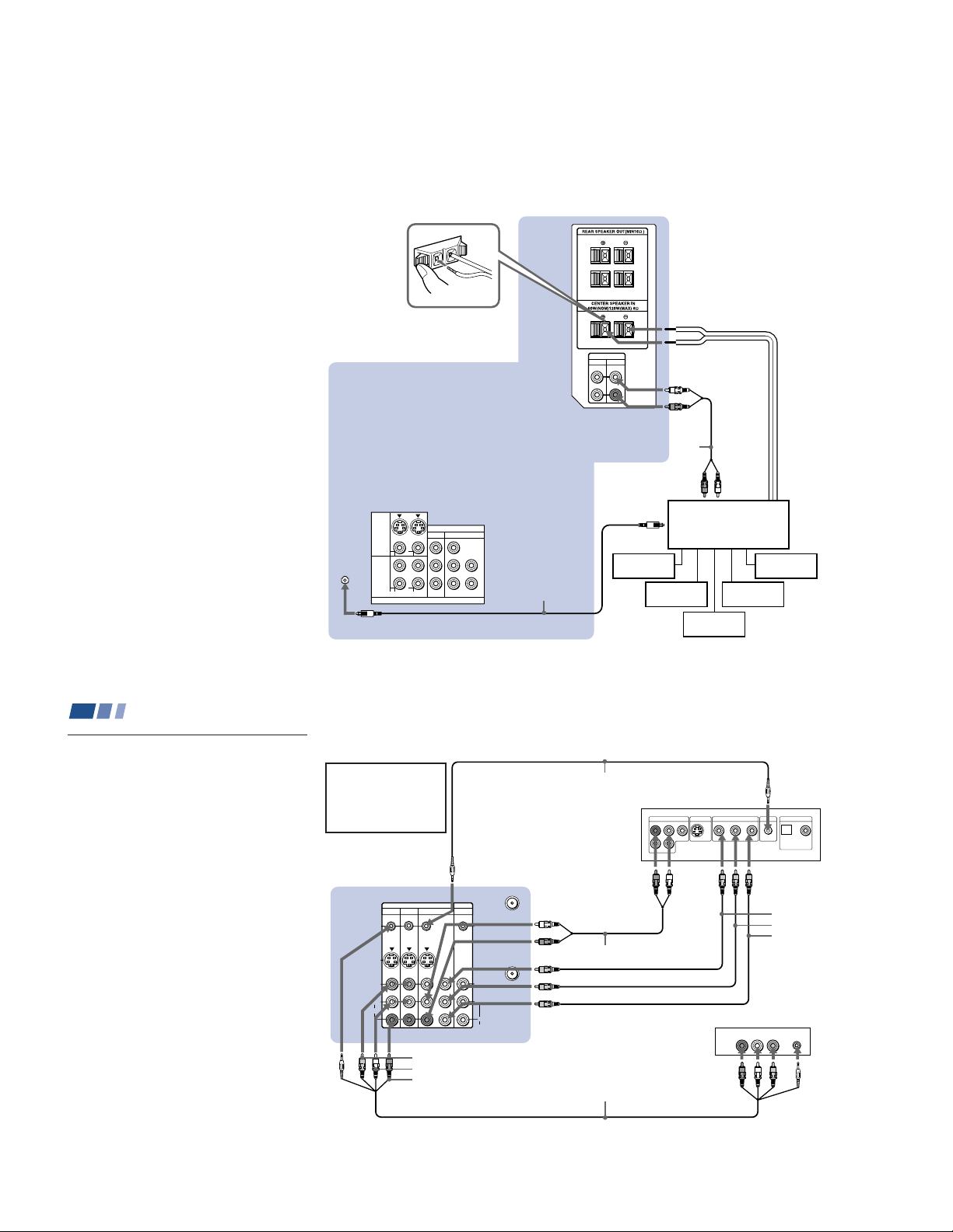
Using the S-Link function with a
S VIDEO
S-LINK/
CONTROL S
OUT
S-LINK/
CONTROL S
IN
VIDEO
AUDIO
L
R
R
VIDEO
(MONO)
IN
SYNC AUDIO
OUT
VIDEO 1 VIDEO 3 VIDEO 4 (DVD)
VIDEO 5 (HD) IN
SELECT
Y
P
B
P
R
YPBP
RYPBPR
RGB
BGR
VD
HD
R
L
L
AUDIO
VHF/UHF
AUX
Sony AV receiver
1 Using a VIDEO cable, connect VIDEO 1
IN on the TV’s upper panel to MONITOR
OUT on the Sony AV receiver.
2 Using an AUDIO/VIDEO cable, connect
SELECT OUT on the TV’s upper panel to
TV AUDIO and VIDEO IN on the AV
receiver.
3 Using an S-LINK cable, connect S-LINK
on the VIDEO 1 IN panel on the TV’s
upper panel and S-LINK on MONITOR
OUT on the AV receiver.
4 Using an S-LINK cable, connect S-LINK
on the SELECT OUT panel on the TV’s
upper panel to S-LINK on TV IN on the
AV receiver.
5 Using AUDIO/VIDEO and S-LINK
cables, connect the Sony video equipment
to the AV receiver.
6 Use the AUDIO menu to set SPEAKER to
ALL OFF or CENTER IN. (see
“SPEAKER” on page 49)
7 Use the SET UP menu to set SELECT
OUT to TV OUT. (see “SELECT OUT” on
page 60)
8 Press CH (CHANNEL) +/– to activate
the S-Link function.
VCR 1
Audio/
video
outputs
Audio/
video
outputs
(Rear of projection TV)
S-LINK/
CONTROL S
OUT
S VIDEO
VIDEO
L
(MONO)
AUDIO
R
VIDEO 1 IN VIDEO
AUDIO R AUDIO L VIDEO
LINE
OUT
VCR 2
AUDIO R AUDIO L VIDEO S-LINK
LINE
OUT
Disconnect all power sources before making any connections.
IN OUT
VIDEO 1 VIDEO 3 VIDEO 4 (DVD) SELECT
Y
P
B
PR
Video cable
(not supplied)
S-LINK
S-LINK
VIDEO 1
Audio/video/
S-Link cable
(not supplied)
S-LINK
S-LINK
AUX
S-LINK/
CONTROL S
IN
VHF/UHF
VIDEO
L
R
AUDIO
S-LINK SELECT OUT
SELECT OUT
RK-G34, etc. (not
supplied)
3
MONITOR OUT
1
(video output)
VIDEO 1 IN (S-LINK and
video/audio inputs)
5
Refer also to the Operating
Instructions supplied with the VCR,
DBS tuner, DVD player, LD player
and other Sony video equipment for
details.
2, 4
MONITOR OUT
S-LINK
VIDEO 2 IN (S-LINK
and video/audio
inputs)
Audio/video/
S-Link cable
(not supplied)
TV IN
(S-LINK and
video/audio
inputs)
Sony AV receiver
21
Installing and Connecting the Projection TV (continued)
Using the CONTROL S feature
CONTROL S allows you to control the
projection TV and other Sony equipment
with one remote control.
To control other Sony equipment with the
projection TV's remote control, connect the
CONTROL S IN jack of the equipment to the
CONTROL S OUT jack on the TV’s upper
panel with the CONTROL S cable.
To control the projection TV with a remote
control for another Sony product, connect the
CONTROL S OUT jack of the equipment to
the CONTROL S IN jack on the TV’s upper
panel with the CONTROL S cable.
About the VIDEO 5 (HD) IN
jacks
The VIDEO 5 (HD) IN jacks on the TV’s
upper panel are designed to connect to the
HDTV output jacks of the equipment which
will accept the various HDTV formats (up to
1080i) scheduled to broadcast in the near
future. The projection TV will be capable of
connecting to a digital cable box TV decoder,
HDTV digital satellite system (DSS) decoder,
etc.
Before operating, set the YP
switch to YP
BPR or RGB depending on the
22
BPR/RGB select
Disconnect all power sources before making any connections.
(Rear of projection TV)
VIDEO 1 VIDEO 3 VIDEO 4 (DVD) SELECT
S-LINK/
CONTROL S
OUT
S VIDEO
VIDEO
L
(MONO)
AUDIO
R
IN OUT
Y
P
PR
AUX
S-LINK/
CONTROL S
IN
VHF/UHF
VIDEO
B
L
R
AUDIO
HDTV equipment which is to be connected.
For details on using the YPBPR/RGB select
switch and the SYNC jacks, refer to the
instruction manual supplied with the HDTV
equipment.
Note:
• The VIDEO 5 (HD) IN jacks are not
compatible with a computer’s 5BNC (R/
G/B/HD/VD) video output connectors.
Do not connect a computer to the VIDEO
5 (HD) IN jacks.
– 15 –
IN
VIDEO 1 VIDEO 3
S-LINK/
CONTROL S
OUT
Do not use the CONTROL S IN/
OUT jacks on the TV’s lower
side panel.
It may cause a malfunction.
VIDEO 4 (DVD) SELECT
(Rear of projection TV)
OUT
S-LINK/
CONTROL S
IN
Page 16
Basic Set Up
TV/VIDEO
SET
UP
TVANT/
DVD ANT
POWER
CHANNEL
VOLUME
+
–
+
–
POWER
Using the Remote Control
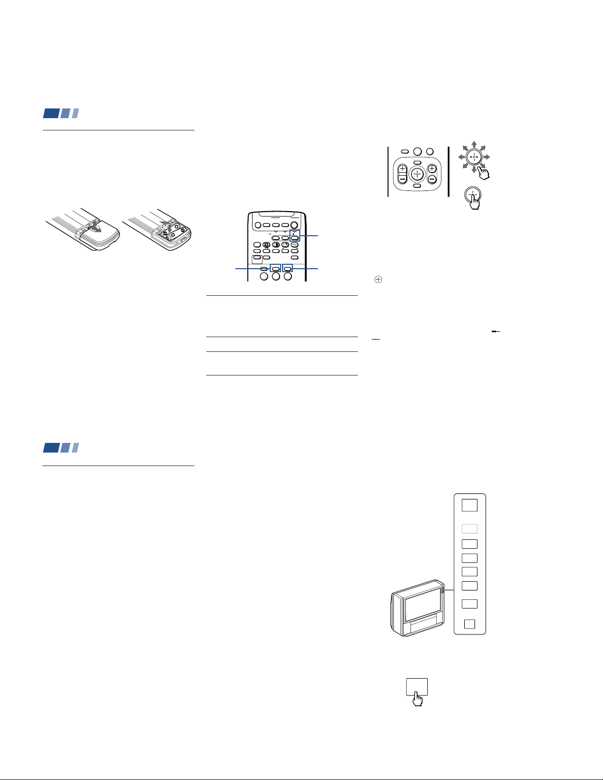
Inserting the batteries
Insert two size AA (R6) batteries (supplied)
by matching the + and – on the batteries to
the diagram inside the remote control’s
battery compartment.
Notes:
• Remove the batteries to avoid damage
from possible battery leakage whenever
you anticipate that the remote control
will not be used for an extended period.
• Handle the remote control with care.
Avoid dropping it, getting it wet, or
placing it in direct sunlight, near a heater
or where the humidity is high.
• Your remote control can be programmed to
operate most video equipment.
(see “Operating Video Equipment” on
page 72)
Selecting a digital TV or
conventional TV program
The remote control functions both for digital
TV and conventional TV features. You will
need to switch the function of the remote
control according to your choice for viewing
either a digital TV or conventional TV
program.
POWER
DVD/
DBS/
DTV ANT
When you use
the remote
control for ......
The Digital TV
The
Conventional TV
MUTING
OFF
WIDE MODE
TV/DBS
PICTURE
MODE
FUNCTION
TV/VIDEO DTV ANT
SLEEP
VTR
CABLE
DVD/VTR
DBS/CABLE
CC
DISPLAY
ALTERNATE
VIDEO AUDIO
JUMP GUIDE
TV ANT
213
Press ....
DTV ANT
TV ANT
TV
TV
so that the TV
FUNCTION
indicator lights
up in .........
green
red
TV
FUNCTION
indicator
TV ANT
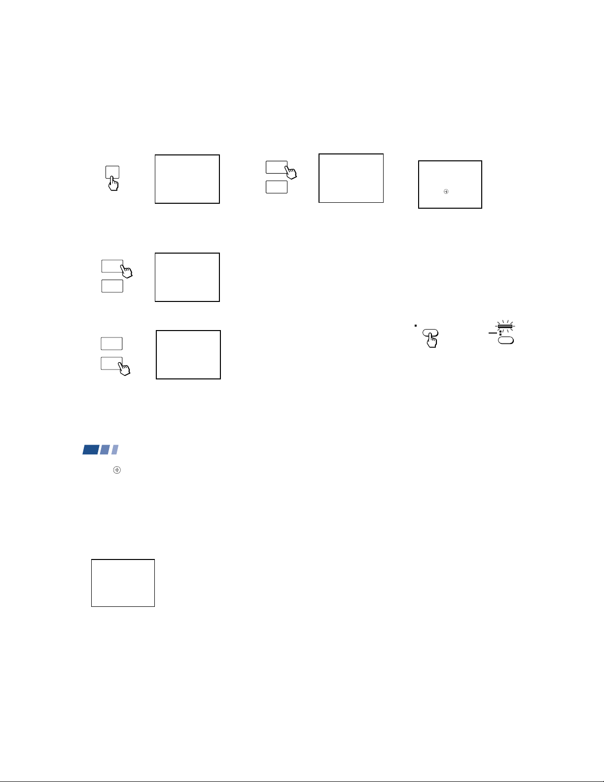
Using the remote control joystick
0
The supplied remote control has a joystick
which moves the on-screen selector in eight
directions. In most cases, moving the joystick
up, down, left or right will cause the selector
to move in the selected direction.
In some cases, the selector may move in
eight directions according to the function.
Pressing down on the center of the joystick
) will activate the selected item.
(
You may also move the joystick right to
activate a selected item. (There are some
exceptions to this option.)
Move
.
Select
Adjusting Sliders
When menu items present a slider ( or
), move the joystick up, down, left or
right to adjust the setting.
On Line Help/Instructions
Several menu windows will provide prompts
and instructions to assist you in navigating
through the different functions.
23
Basic Set Up (continued)
Setting Up the Projection TV
Automatically
The AUTO SET UP feature will allow you to
set all receivable channels.
First, perform AUTO SET UP for
conventional TV programs. You can also set
the on-screen language.
After AUTO SET UP is completed for
conventional TV programs, Auto Program
will automatically run for digital TV
programs. Later, verify the Language and
Time Zone settings in your DTV Setup Menu.
(for details, see pages 34 and 35)
The AUTO SET UP feature does not apply
for installations that use a cable box for all
channel selection.
You can also set up the projection TV manually.
(see “Channel Setup” on page 33 for digital TV
channels, or “Using the CHANNEL SET UP
Menu” on page 54 for conventional TV channels)
24
Notes:
• Perform this function during the day, with
the antenna and/or cable properly
connected, to ensure that all available
channels will be broadcasting and
receivable.
• Before you perform AUTO SET UP for
conventional TV programs, make sure
that the input from ANT (not AUX) is
selected by pressing TV ANT until “AUX”
does not appear next to the channel
number.
• When you perform AUTO SET UP for
conventional TV programs, your
CHANNEL FIX and ON/OFF TIMER
settings will be erased.
• When you perform AUTO SET UP for
conventional TV programs, the settings in
the VIDEO menu except for “NR,”
“COLOR CORRECTION” and “DC
TRANSMISSION” and all the settings in
the AUDIO menu are reset to the factory
settings.
– 16 –
First, perform AUTO SET UP for conventional
TV programs by using the buttons on the upper
right side panel on the front of the projection TV.
1 Press POWER to turn on the projection
TV.
Page 17
2 Press SET UP to display the AUTO SET
DTV ANT
TVFUNCTION
OK
CANCEL
Welcome to DTV!
Before you can view DTV programs, you
must run Auto Program.
Press to continue.
Please check the
Time Zone setting later.
UP screen for conventional TV programs.
SET
ENGLISH :
ESPAÑOL :
UP
AUTO SET UP :
DTV SET UP :
First please connect
the antenna.
Press [ SET UP ] to exit.
[ CH + ]
[ CH – ]
[ VOL – ]
[ TV / VIDEO ]
3 Press CHANNEL + to select English,
CHANNEL – to select Spanish.
The screen will change to reflect your
choice.
+
CHANNEL
–
ENGLISH :
ESPAÑOL :
AUTO SET UP :
DTV SET UP :
First please connect
the antenna.
Press [ SET UP ] to exit.
[ CH + ]
[ CH – ]
[ VOL – ]
[ TV / VIDEO ]
4 Press VOLUME – to select “AUTO SET
UP.”
+
VOLUME
CONTINUE TO
AUTO PROGRAM ?
[ CH + ]
YES :
[ CH – ]
NO :
–
5 Press CHANNEL + to preset
conventional TV channels automatically.
+
CHANNEL
AUTO PROGRAM
–
“AUTO PROGRAM” appears and the
projection TV starts scanning and
presetting conventional TV channels
automatically. While scanning, the
received conventional TV channel will be
displayed on the sub screen. When all the
receivable channels are stored, the lowest
conventional TV channel number will be
displayed. If the projection TV receives
cable TV channels, CABLE is set to ON
automatically.
After AUTO SET UP for conventional TV
programs has been completed, the Initial Setup
screen for digital TV programs will appear.
Second, perform Auto Program for digital TV
programs by using the buttons on the remote
control.
6 Press DTV ANT on the remote control so
that the TV FUNCTION indicator lights
up in green momentarily.
The remote control functions for digital
TV programs.
Auto Program for digital TV begins.
Lights up in
green.
(continued)
25
Basic Set Up (continued)
7 Press (press down on the center of the
joystick) to start Auto Program for digital
TV.
“Auto Program in Progress...” is
displayed as the projection TV scans and
presets available digital TV programs.
When all the receivable channels are
stored, the lowest digital channel number
will be displayed.
Auto Program in Progress...
26
To perform AUTO SET UP again
Press SET UP. Perform as described in steps
3–7 on pages 25 and 26. Press SET UP again
to exit.
– 17 –
Page 18
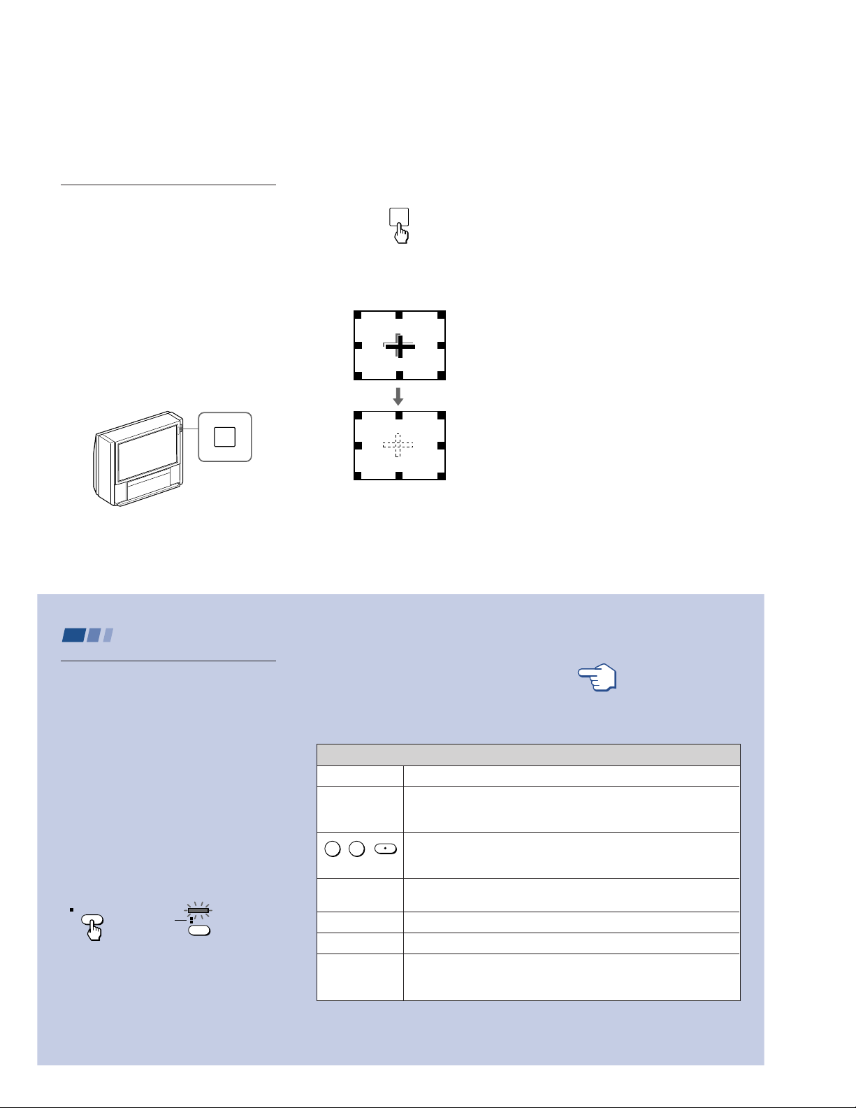
Adjusting the Convergence
TVFUNCTION
Automatically (AUTO FOCUS)
The projection tube image appears on the
screen in three layers (red, green and blue). If
they do not converge, the color is poor and
the picture blurs.
Before you use your projection TV, be sure to
adjust the convergence.
The AUTO FOCUS feature allows you to
adjust the convergence automatically.
Tip
z
• It is recommended to perform AUTO FOCUS about
30 minutes after the projection TV is first turned on.
AUTO
FOCUS
Press AUTO FOCUS.
AUTO
FOCUS
The cross pattern appears and AUTO FOCUS
begins to work. The adjustment is completed
when the cross pattern becomes white.
Note:
• You cannot perform any other functions
until AUTO FOCUS has completed its
cycle.
27
Using Digital TV Features
Watching Digital TV
Many digital TV features can be accessed
directly through the remote control. The
following chart will explain the function of
some buttons found on your remote control.
To use the remote control for
digital TV programs
First, press DTV ANT on the remote control
so that the TV FUNCTION indicator on the
remote control lights up in green
momentarily.
The remote control functions for digital TV
programs.
At the same time the DTV indicator on the
front of the projection TV lights up in green.
DTV ANT
Make sure that the TV FUNCTION indicator
lights up in green each time you press the
buttons listed in the tables.
28
Lights up in
green.
REMOTE CONTROL ON THE
INSIDE FRONT COVER OF
Using the White Labeled Buttons for Projection TV Operations
TV (FUNCTION)
TV POWER
-
0 9
and ENTER
,
GUIDE
CH +/–
VOL +/–
JUMP
Activates the remote control for use with the projection TV.
Turns the projection TV on and off. If a video input indication (e.g. VIDEO 1,
VIDEO 2) appears on the screen, press TV/VIDEO until a channel number
appears.
Use for direct digital channel selection. Digital channels are indicated by the
use of a dot in the channel number. For example, to select subchannel 3 in
main channel 10 (channel number 10.3), press 1, 0, • (dot), 3 and ENTER.
Press to display the Program Guide. (see “Using Program Guide to Select
Subchannels” on page 31)
Press to scan through the channels (+ up or – down).
Press to adjust the volume (+ up or – down).
Press to alternate or
projection TV will jump between the current channel and the last channel
selected using the 0–9 and • (dot) buttons, CH+/– buttons or Program Guide.
jump
back and forth between two digital channels. The
REFER TO THE
ILLUSTRATION OF THE
THIS MANUAL AS YOU
REVIEW THIS CHART
(continued)
– 18 –
Page 19
Using the White Labeled Buttons for Projection TV Operations
WIDE MODE
WIDE MODE
MUTING
SLEEP
DISPLAY
or
CC
TV/VIDEO
Tip
z
You can adjust the picture and sound qualities using
the VIDEO (page 47) and AUDIO (page 49) menus
even when you are watching a digital TV program.
Before operating the menu, press TV (FUNCTION) so
that the TV FUNCTION indicator lights up in red.
After finishing the menu operation, press TV
(FUNCTION) again to make the TV FUNCTION
indicator light up in green.
Press to watch 4:3 normal broadcasts in wide screen mode (16:9 aspect
ratio). (see “Using the Wide Screen Mode” on page 30)
Press to mute the sound. “MUTING” will appear on the screen and will dim
three seconds later. To restore sound, press again or press VOL +.
Press repeatedly until the projection TV displays the approximate time in
minutes (30, 60 or 90) that you want the projection TV to remain on before
shutting off automatically.
Cancel by pressing until “SLEEP OFF” appears.
Each press scrolls through the following indications:
n
Channel number, name and logo (if set) and current time
n
Closed caption
n
Display off
Press repeatedly to scroll through available video inputs:
TV, VIDEO 1, VIDEO 2, VIDEO 3, VIDEO 4 and VIDEO 5.
REFER TO THE
ILLUSTRATION OF THE
REMOTE CONTROL ON THE
INSIDE FRONT COVER OF
THIS MANUAL AS YOU
REVIEW THIS CHART
29
Using Digital TV Features (continued)
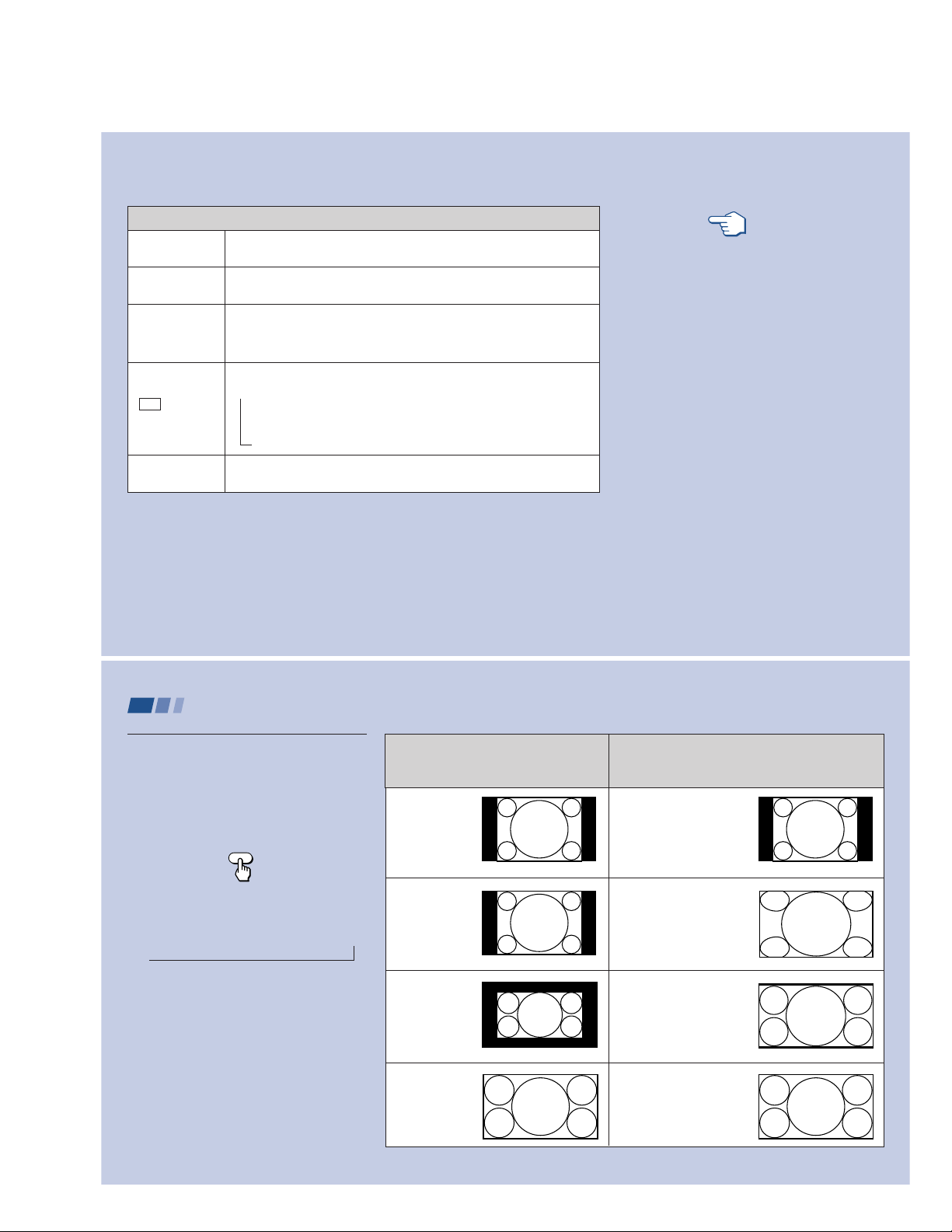
Using the Wide Screen Mode
The wide screen mode feature lets you watch
4:3 normal broadcasts in wide screen mode
(16:9 aspect ratio).
Press WIDE MODE on the remote control.
Each press scrolls through the following
modes:
NORMALnWIDE ZOOMnZOOMnFULL
n
Notes:
• The AUTO WIDE feature lets you select
the most suitable mode automatically for
a picture containing an aspect ratio
signal. (see “AUTO WIDE” on page 53)
• For ZOOM and WIDE ZOOM modes you
can adjust the vertical position of the
picture. (see “V CENTER” on page 53)
30
To watch the original
broadcasting screen sizes
shown below
DTV 4:3 aspect
ratio picture
DTV 4:3 aspect
ratio picture
Letter box movie
of a video tape or
a DVD disc
DTV 16:9 aspect
ratio picture
Press WIDE MODE to select the altered
screen sizes shown below
NORMAL
Select to return the 4:3
picture to normal mode.
WIDE ZOOM
Select to enlarge the 4:3
picture, while the upper and
lower parts of the picture are
condensed to fit the 16:9
screen.
ZOOM
Select to enlarge the 4:3
picture horizontally and
vertically to an equal aspect
ratio that fills the 16:9
screen.
FULL
No change
(DTV 16:9 aspect ratio
picture is always displayed
in FULL mode.)
– 19 –
Page 20
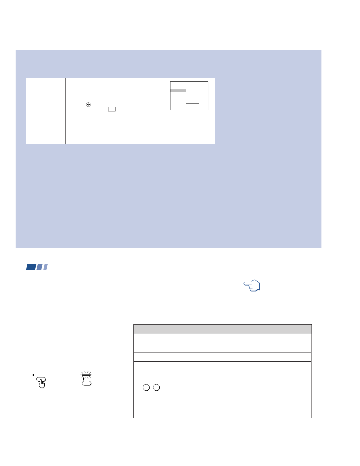
Using the Program Guide to
MENU
Channel Setup
Caption Vision
Language
Auto Program
DTV Auto Add
Name and Logo
Skip/Add
Time Zone
Channel Setup
Caption Vision
Language
English
Spanish
Select Subchannels
The Program Guide lets you select
subchannels from an on-screen list.
Subchannels are additional channels of
programming that are broadcast
simultaneously by a single network. For
example, channel 2, a main channel, might
include four subchannels (2.1, 2.2, 2.3 and
2.4) that are showing programs at the same
time.
1 Press GUIDE.
If the projection TV is tuned to a DTV
channel, the program guide appears. The
currently selected subchannel is
highlighted.
CH 2.2
30 PBS
GUIDE
Channels that include subchannels include a dot,
followed by the number of the subchannel, such as
“2.1,” etc.
To check the channel number, press DISPLAY.
2 ABC
3 CBS
5 FOX
16 UPN
20 WB
25 NBC
.1 Drew Carey
.2 ABC movie
.3 News @ 8:00
.4 Ellen
Program information in the program guide is
provided by the broadcasters. As a result, the
program guide may sometimes include only the
channel number without a program title, station
logo or description.
2 Move the joystick left to select the main
channel list.
CH 2.2
.1 Drew Carey
30 PBS
.2 ABC movie
2 ABC
.3 News @ 8:00
3 CBS
.4 Ellen
5 FOX
16 UPN
20 WB
25 NBC
3 Move the joystick up or down to select the
desired main channel number.
The tuning indicator appears. When the
selected main channel is tuned in, all of
the subchannels are listed. The first
subchannel is highlighted and its program
information appears at the top of the
screen.
CH 5.1
3 CBS
5 FOX
16 UPN
20 WB
25 NBC
30 PBS
2 ABC
.1 The X-files
.2 Party of five
.3 Ally Mc Beal
.4 Simpsons
4 Move the joystick up or down to select
the desired subchannel, and press
The program guide will disappear.
To clear the program guide without
changing channels
Press GUIDE.
.
31
Using Digital TV Features (continued)
Learning Setup Menu Selection
Use the MENU button to access the setup
menu and use the joystick to alter settings.
Use the following example to learn how to
modify settings.
1 Press the MENU button.
The setup menu appears.
MENU
2 Move the joystick up or down to select the
desired setup item.
Information about the selected
item is displayed here.
Pop-up menu
Options for your selection (pop-up menu
on the right) will be displayed.
32
3 Press (press down on the center of the
joystick) to activate the selected item.
The currently selected option is
highlighted and marked with a check
).
mark (
Channel Setup
English
Caption Vision
Spanish
Language
You may also move the joystick right to
activate a selection.
4 Move the joystick up or down to select
the desired option, and press .
The selected option is highlighted and
marked with a check mark. The current
selection is displayed at the top of the onscreen menu.
Prog. de canales
English
Caption Vision
Spanish
Idioma
– 20 –
Some options may require further
operations.
For details, see each menu option.
5 Once you have completed all menu
settings, press MENU to exit the menu
screens.
You may also move the joystick left to
return to the previous screen.
To exit from the menus at any time
Press MENU.
Page 21
Using the Setup Menu
Name and Logo
Press CH+/– to change channels.
Press
“ ”
to toggle Name/Logo.
OK
Cancel
Channel 30 FOX
FOX
Channel Setup
Auto Program
Caption Vision
DTV Auto Add
Language
Name and Logo
Skip/Add
Time Zone
For detailed information on using the remote
control to modify menu settings, refer to
“Learning Setup Menu Selection” on page 32.
Channel Setup
Basic channel and
display options
Auto Program: Select to scan and preset digital channels automatically. Before
“Auto Program” process, a dialog box pops up with the message “Are you sure
you want to clear your existing channel list?” Move the joystick left or right to
select OK, and press to activate “Auto Program.” A tuning indicator appears
and the projection TV starts scanning and presetting digital channels
automatically. When all the receivable channels are stored, the lowest channel
is displayed and the tuning indicator disappears.
Note:
• If you currently have a list of programmed channels, or “Name and Logo” or
“Skip/Add” setting, they will be erased when you perform “Auto Program.”
DTV Auto Add: Select to preset additional digital channels as they become
available without erasing original channels (after you use Auto Program).
During the “DTV Auto Add” process, a tuning indicator appears and the
projection TV starts scanning and adding new digital channels. When scanning
is complete, the indicator disappears and the current channel re-appears.
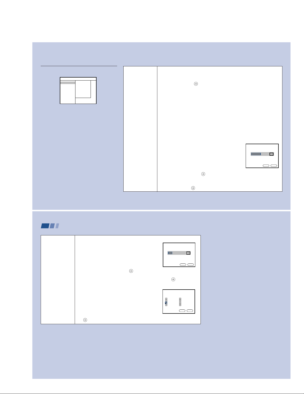
Name and Logo: Select to add or change the station
Dialog box
name and logo.
When selected, a dialog box pops up.
1 Press CH +/– to select the desired channel.
2 Move the joystick left or right to select the station
name and the corresponding logo.
3 Move the joystick up or down—and then left or right—
to select OK, and press .
To clear the dialog box without changing the name and logo for the current
channel, move the joystick up or down—and then left or right—to select
“Cancel,” and press .
(continued)
33
Using Digital TV Features (continued)
Channel Setup
Basic channel and
display options
Skip/Add: Select to erase or add channels from/to
your channel list.
When selected, a dialog box pops up.
1 Press CH +/– to select the desired channel.
2 Move the joystick left or right to select Skip to erase
a channel, or select Add to add a channel.
3 Move the joystick up or down—and then left or
right—to select OK, and press .
To clear the dialog box without erasing/adding a channel, move the joystick up
or down—and then left or right—to select “Cancel” and press .
Time Zone: Digital channels include time signals
based on the time zone. Select to choose a time zone
for your area.
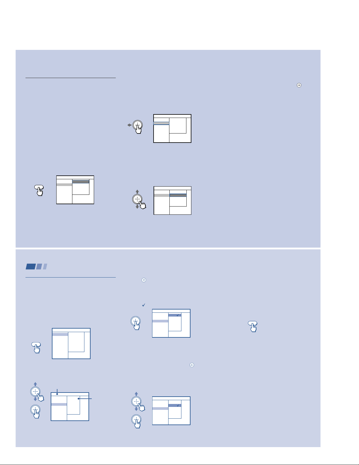
When selected, the time zone dialog box pops up.
1 Move the joystick up, down, left or right to choose
your time zone.
A check mark will be given to your selection.
2 Move the joystick left or right to select OK, and press
.
34
Dialog box
Dialog box
– 21 –
Skip / Add
Skip CH30 FOX
Press CH+/– to change channels.
Press
“ ”
to toggle Skip/Add.
OK
Please select your appropriate
Time Zone
ARIZONA(mountain)
EASTERN
PACIFIC
INDIANA(eastern)
ALASKA
CENTRAL
HAWAI
MOUNTAIN
OK
(continued)
FOX
Cancel
Cancel
Page 22
Caption Vision
Television closed
caption display
Some programs are broadcast with Caption Vision
(closed caption).
To display closed caption
1 Select your language (English or Spanish) and then
press on the remote control.
2 Press DISPLAY or CC until the Caption Vision
appears.
Channel Setup
Caption Vision
Language
English
Spanish
Language
User’s preferred
language
Select from available languages (English or Spanish) to display the DTV Setup
menus in your language of choice.
Using Conventional TV Features
Watching Conventional TV
Many Conventional TV features can be
accessed directly through the remote control.
The following chart will explain the function
of some buttons found on your remote
control.
To use the remote control for
conventional TV programs (VHF/
UHF and AUX inputs)
First, press TV ANT on the remote control so
that the TV FUNCTION indicator on the
remote control lights up in red momentarily.
The remote control functions for
conventional TV programs.
TV ANT
Make sure that the TV FUNCTION indicator
lights up in red each time you press the
buttons listed in the tables.
TVFUNCTION
Lights up
in red.
REMOTE CONTROL ON THE
INSIDE FRONT COVER OF
THIS MANUAL AS YOU
Using the White Labeled Buttons for Projection TV Operations
TV ANT
(AUX input)
TV (FUNCTION)
TV POWER
-
0 9
and ENTER
CH +/–
VOL +/–
Press to change between the VHF/UHF input and the AUX input. (for
detailed connection information, see “Cable and antenna” on page 7 or
“Cable box and cable” on page 8)
Activates the remote control for use with the projection TV.
Turns the projection TV on and off. If a video input indication (e.g., VIDEO 1,
VIDEO 2) appears on the screen, press TV/VIDEO until a channel number
appears.
Use for direct conventional TV channel selection. Press 0-9 to select a
channel (for example, to select channel 10, press 1 and 0). The channel will
change after 2 seconds, or you can press ENTER for immediate selection.
Press to scan through the channels (+ up or – down).
Press to adjust the volume (+ up or – down).
35
REFER TO THE
ILLUSTRATION OF THE
REVIEW THIS CHART
(continued)
36
– 22 –
Page 23
Using the White Labeled Buttons for Projection TV Operations
JUMP
WIDE MODE
(Wide screen
mode)
MUTING
FREEZE
(yellow labeled
button)
SLEEP
DISPLAY
Press to alternate or
channels. The projection TV will jump between the current channel and the last
channel selected using the 0-9 buttons.
Press to watch 4:3 normal broadcasts in wide screen mode (16:9 aspect
ratio). (see “Using the Wide Screen Mode” on page 39)
Press to mute the sound. “MUTING” will appear on the screen and will
dim three seconds later. To restore sound, press again or press VOL +.
This is useful when you need to copy down information that appears on
the TV’s screen.
Press to
freeze
Press again or press (OFF) to cancel.
If you select TWIN as a FREEZE MODE in the SET UP menu, you can
freeze the desired scene and display it on the left while viewing the
normal picture on the right. (see “FREEZE MODE” on page 63)
Note: If the frozen picture mode is not canceled for more than an hour,
the normal picture is resumed automatically.
Press repeatedly until the projection TV displays the approximate time in
minutes (30, 60, or 90) that you want the projection TV to remain on before
shutting off automatically.
Cancel by pressing until “SLEEP OFF” appears.
Press to display the channel number, current time, channel caption (if
set), and MTS mode (if SAP is selected). The SAP indication disappears
and the other indications dim three seconds later.
To turn the display off, press DISPLAY again.
jump
back and forth between two conventional TV
the picture.
(continued)
PICTURE MODE
Press PICTURE MODE repeatedly to directly
choose one of five different video modes that
best suits the program you are watching.
You can also adjust the picture quality (such as
BRIGHTNESS, COLOR, etc.) for each mode to
suit your taste.
First select each MODE individually before
adjusting the picture quality.
VIVID: Select for enhanced picture contrast and
sharpness.
STANDARD: Select to display a standard
picture for normal viewing environments.
MOVIE: Select to display a finely detailed
picture for low light environments.
GAME: Select to display graphics such as a
video game.
PRO (Professional): Select to display a picture
with minimum enhancements.
For details, see “MODE” on page 47.
37
Using Conventional TV Features (continued)
Using the White Labeled Buttons for Projection TV Operations
CC
TV/VIDEO
MTS
38
Press repeatedly to scroll through available displays:
XDS (Extended Data Service)
Displays a network name, program name, program type, program length,
program description, call letters and time of the show if the broadcaster
offers this service.
Caption Vision
Displayed on the screen if the broadcaster offers this service. (see
“CAPTION VISION” on page 59)
No display
“OFF” appears and the display is canceled.
Press repeatedly to scroll through available video inputs:
TV, VIDEO 1, VIDEO 2, VIDEO 3, VIDEO 4 and VIDEO 5
If you select SKIP as a VIDEO LABEL in the SET UP menu, your projection
TV will skip the video input you selected. (see “VIDEO LABEL” on page 61)
Press to scroll through the Multi-channel TV Sound (MTS) options.
(see “MTS” on page 49)
REFER TO THE
ILLUSTRATION OF THE
REMOTE CONTROL ON THE
INSIDE FRONT COVER OF
THIS MANUAL AS YOU
REVIEW THIS CHART
– 23 –
Page 24
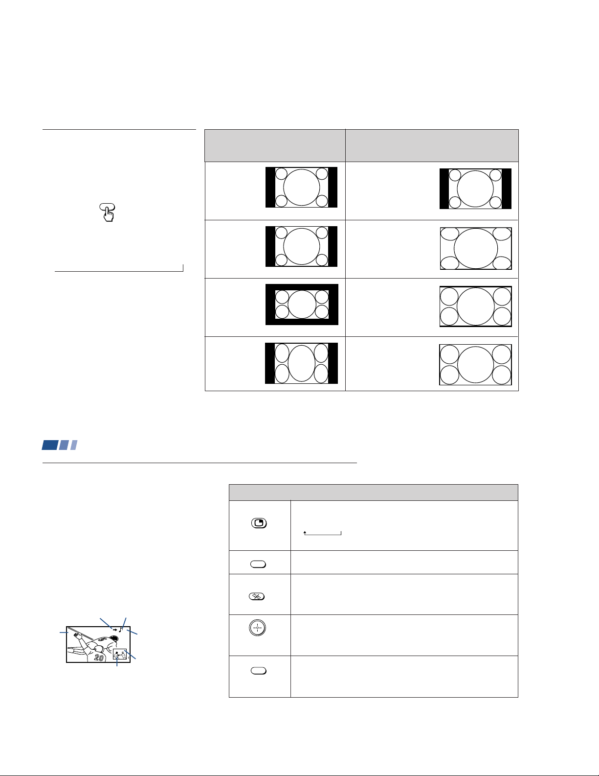
Using the Wide Screen Mode
WIDE MODE
The wide screen mode feature lets you watch
4:3 normal broadcasts in wide screen mode
(16:9 aspect ratio).
Press WIDE MODE on the remote control.
To watch the original
broadcasting screen sizes
shown below
Normal 4:3
aspect ratio
picture
Press WIDE MODE to select the altered
screen sizes shown below
NORMAL
Select to return the 4:3
picture to normal mode.
Normal 4:3
Each press scrolls through the following
modes:
aspect ratio
picture
NORMAL n WIDE ZOOM n ZOOM n FULL
n
Notes:
• The AUTO WIDE feature lets you select
the most suitable mode automatically for a
Letter box movie
of a video tape or
a DVD disc
picture containing an aspect ratio signal.
(see “Using AUTO WIDE” on page 53)
• For ZOOM and WIDE ZOOM modes you
can adjust the vertical position of the
picture. (see “V CENTER” on page 53)
4:3 squeezed
video camera or
DVD picture
Using Conventional TV Features (continued)
Watching Two Programs at One Time — PIP
The Picture-in-Picture (PIP) feature allows
you to view two channels simultaneously,
one in the full size “main” picture and one in
a smaller “window” picture.
You can move the window picture to any
location on the screen.
Note:
• The PIP feature is not available for the
inputs from VIDEO 5 IN and for digital
TV programs.
The symbol “b” or “B”
indicates which picture's
TV channel or input
source can be changed.
Main
picture
Tip
z
If you press RESET in PIP mode, the window picture
will move to the bottom right (factory-preset location).
The symbol “≥”
indicates which
picture's sound is being
received.
TV channel or inputsource mode for the
6
main picture (It will
dim in about 3
seconds.)
10
TV channel or input-
Window
picture
source mode for the
window picture (It
will dim in about 3
seconds.)
40
POSITION
ACTIVE
(white labeled
button)
TV/VIDEO
(white labeled
button)
WIDE ZOOM
Select to enlarge the 4:3
picture, while the upper and
lower parts of the picture
are condensed to fit the
16:9 screen.
ZOOM
Select to enlarge the 4:3
picture horizontally and
vertically to an equal aspect
ratio that fills the 16:9
screen.
FULL
Select to enlarge the 4:3
picture horizontally only, to
fill the 16:9 screen.
39
Using the Yellow Labeled Buttons for PIP Operations
Press to display a window picture.
Each time you press this button, the picture size will change
(1/4 n1/9 n1/16).
Press (OFF) to close the window picture.
Press to change the location of the window picture (counterclockwise)
around the main picture.
Press to select either the main or window picture in order to change the
TV channel or video source using the white labeled buttons below. The
symbol “b” (or “B”) will appear to indicate which picture’s channel or input
mode can be changed.
To change the location of the window picture, move the joystick in any
direction and release it when the picture is in the desired location.
Press repeatedly to scroll through the available video inputs for the picture
on which the symbol “b” (or “B”) is displayed. (see “TV/VIDEO” on page
38)
(continued)
– 24 –
Page 25
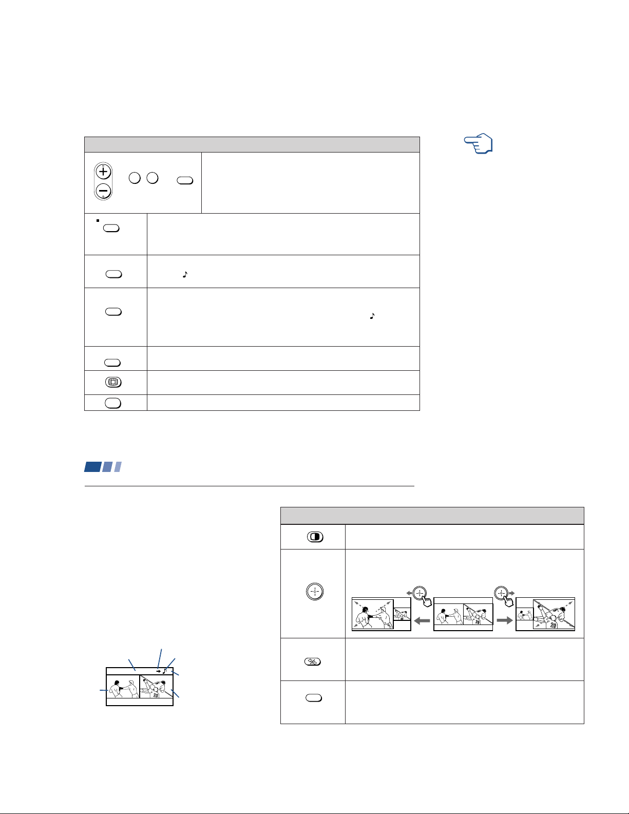
Using the Yellow Labeled Buttons for PIP Operations
AUDIO
CH
or or
-
0 9
and ENTER
(white labeled button)
TV ANT
(white labeled
button)
FREEZE
SWAP
OFF
Press to select the TV channel on which the symbol “b” (or “B”) is
JUMP
Press to change between the VHF/UHF input and the AUX input for the picture on
which the symbol “b” (or “B”) is displayed.
Press to alternate sound between the main picture and the window picture. The
symbol " " will appear for a few seconds to indicate which picture’s sound is being
received.
This is useful when you need to copy down information that appears on the TV’s
screen.
Press to freeze the main and window pictures. The symbols “b” and " ," and the
channel number disappear.
Press again to resume PIP viewing. Press (OFF) to cancel and resume normal TV
viewing.
Press to switch the audio and video of the main picture and the window picture.
Each time you press SWAP, the picture and sound of the two will be exchanged.
Press to access CHANNEL INDEX for direct channel selection. (see “Using
CHANNEL INDEX” on page 44)
Press to cancel the PIP function and return to normal viewing.
displayed. (for details, see “Watching Conventional TV” on page
36)
REFER TO THE
ILLUSTRATION OF THE
REMOTE CONTROL ON THE
INSIDE FRONT COVER OF
THIS MANUAL AS YOU
REVIEW THIS CHART
Notes:
• If one of the pictures received through
PIP is snowy, the entire screen may
become unstable. In this case, erase the
snowy channel. (see “CHANNEL SKIP/
ADD” on page 54)
• You can change the wide screen mode of
the main picture only. The mode is not
available for the window picture.
• The 16:9 aspect ratio picture with ID-1 or
S1 is always displayed in FULL mode,
even when it is shown as the window
picture.
41
Using Conventional TV Features (continued)
Watching Two Programs at One Time — P&P (Twin ViewTM)
The Picture-and-Picture (P&P) feature allows
you to view two channels simultaneously,
both in a reduced size screen. The main
picture will appear on the right.
You can change the size of both pictures to
suit your personal preference.
Note:
• The P&P feature is not available for the
inputs from VIDEO 5 IN and for digital
TV programs.
The symbol “b” or “B”
TV channel or
input-source mode
for the sub picture
(It will dim in
about 3 seconds.)
Sub
picture
Tip
z
If you press RESET in P&P mode, the right and left
pictures will be reset to the same size (factory-preset
size.)
indicates which picture's TV
channel or input source can be
changed.
The symbol “≥” indicates
which picture's sound is
being received.
TV channel or input-
67
source mode for the main
picture (It will dim in
about 3 seconds.)
Main picture
42
Using the Yellow Labeled Buttons for P&P Operations
Press to display right (main) and left pictures.
Press (OFF) to close the window picture.
Move the joystick right to zoom in on the right picture, and left to zoom in
on the left picture. Release at the desired size. The other picture will be
zoomed out simultaneously.
ACTIVE
TV/VIDEO
(white labeled
button)
Press to select either the right or left picture in order to change the TV
channel or video source using the white labeled buttons below. The
symbol “b” (or “B”) will appear to indicate which picture’s channel or input
mode can be changed.
Press repeatedly to scroll through the available video inputs for the picture
on which the symbol “b” (or “B”) is displayed. (see “TV/VIDEO” on page
38)
(continued)
– 25 –
Page 26
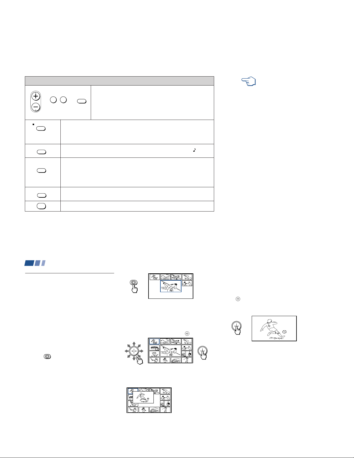
Using the Yellow Labeled Buttons for P&P Operations
CH
or or
-
0 9
and ENTER
(white labeled button)
TV ANT
(white labeled
button)
AUDIO
FREEZE
SWAP
OFF
Press to select the TV channel on which the symbol “b” (or “B”) is
JUMP
Press to change between the VHF/UHF input and the AUX input for the picture on
which the symbol “b” (or “B”) is displayed.
Press to alternate sound between the right and left pictures. The symbol " " will
appear for a few seconds to indicate which picture’s sound is being received.
This is useful when you need to copy down information that appears on the TV’s
screen.
Press to freeze both the right and left pictures.
Press again to resume P&P viewing or press (OFF) to cancel and resume normal
TV viewing.
Press to switch the audio and video of the right and left pictures.
Each time you press SWAP, the picture and sound of the two will be exchanged.
Press to cancel the P&P function and return to normal viewing.
displayed. (for details, see “Watching Conventional TV” on page
36)
REFER TO THE
ILLUSTRATION OF THE
REMOTE CONTROL ON THE
INSIDE FRONT COVER OF
THIS MANUAL AS YOU
Notes:
REVIEW THIS CHART
• If one of the pictures received
through P&P is snowy, the entire
screen may become unstable. In this
case, erase the snowy channel. (see
“CHANNEL SKIP/ADD” on page
54)
• The right and left pictures (except for
the 16:9 aspect ratio signals with ID-1
or S1) are always displayed in an
aspect ratio of 4:3. The WIDE MODE
button on the remote control does not
function with the P&P mode.
• The 16:9 signals with ID-1 or S1 are
always displayed in an aspect ratio of
16:9.
43
Using Conventional TV Features (continued)
Using CHANNEL INDEX
You can use the CHANNEL INDEX feature
to display multiple channels and select one
directly.
Channels used for CHANNEL INDEX will
come directly from the TV’s list of receivable
channels (those set during AUTO
PROGRAM or through the CHANNEL SET
UP menu).
Note:
• The CHANNEL INDEX feature is not
available for the inputs from VIDEO 5 IN
and for digital TV programs.
1 Press .
The current channel will be reduced in
size and displayed in the center of the
screen in normal motion picture format in
FULL wide screen mode. The first twelve
receivable channels, displayed in FULL
wide screen mode, will appear one after
another, clockwise, around the center
picture. These small pictures are updated
in intervals of one second. The channel
number and channel caption (if set) on
the second and later appearances will
dim.
44
10
A cyan-colored frame will appear to
indicate current channel selection.
2 Move the joystick in any direction to
move the cyan frame to the picture that
you wish to view, and press .
Reciipe
flour - - - - 2
sugar - - - 1/2
salt - - - - - 1/2
butter - - - 1
The selected channel will zoom in and
move to the center, and the sound of that
channel will be heard.
Reciipe
flour - - - - 2
sugar - - - 1/2
salt - - - - - 1/2
butter - - - 1
3 If you wish to view another channel,
repeat step 2.
To view the normal picture of the
selected channel, proceed to step 4.
4 Press .
The center picture will be enlarged for
normal viewing.
Notes:
• You cannot move the cyan frame until all
of the surrounding pictures appear.
• The projection TV will continually update
each of the surrounding pictures while
the CHANNEL INDEX screen is
displayed.
• Sound will only be heard from the center
picture.
• If one of the pictures received through
CHANNEL INDEX is snowy, the entire
screen may become unstable. In this case,
erase the snowy channel. (see
“CHANNEL SKIP/ADD” on page 54)
• If you leave the CHANNEL INDEX
screen displayed for an hour without any
additional operation, CHANNEL INDEX
is canceled and the normal picture
reappears.
– 26 –
Page 27
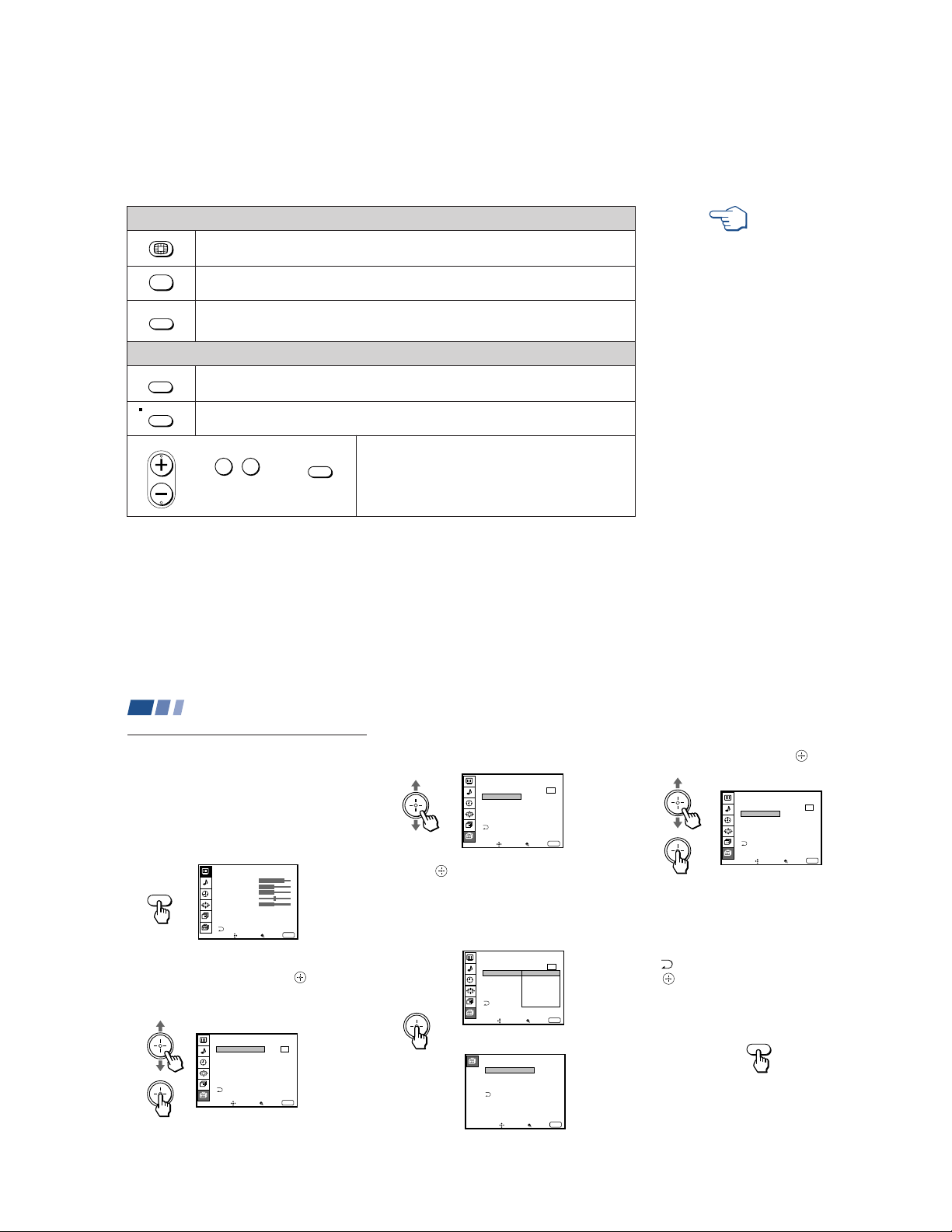
Using the Yellow Labeled Buttons for CHANNEL INDEX Operations
TV ANT
Move Select Exit
MENU
SET UP
PARENTAL CONTROL
CAPTION VISION:
SELECT OUT: VIDEO1
LANGUAGE: ENGLISH
VIDEO LABEL
DIRECT PLAY
FREEZE MODE: NORMAL
CC1
Press to display the next twelve receivable channels.
OFF
Press to cancel the current operation and return to normal TV viewing.
REFER TO THE
ILLUSTRATION OF THE
REMOTE CONTROL ON THE
INSIDE FRONT COVER OF
THIS MANUAL AS YOU
REVIEW THIS CHART
FREEZE
Press to freeze the center picture.
Press again to cancel the frozen picture and resume normal center picture viewing.
Using the White Labeled Buttons for Center Picture Operations
TV/VIDEO
CH
Press to scroll the center picture through the video inputs.
The surrounding channels will not change.
Press to switch the center picture between the VHF/UHF input and the AUX input.
-
0 9
or or
and ENTER
Using Conventional TV Features (continued)
Learning Menu Selection
Use the MENU button to access a menu and
use the joystick to alter the settings. Use the
following example to learn how to modify
settings.
1 Press the MENU button.
The main menu appears.
VIDEO
MODE : VIVID
PICTURE
MENU
2 Move the joystick up or down to highlight
the desired menu and press
down on the center of the joystick) to
activate it.
You may also move the joystick right to
activate your selection.
46
BRIGHTNESS
COLOR
HUE
SHARPNESS
TRINITONE : HIGH
DRC MODE :
ADVANCED VIDEO
Move Select Exit
SET UP
PARENTAL CONTROL
CAPTION VISION:
SELECT OUT: MONITOR
LANGUAGE: ENGLISH
VIDEO LABEL
DIRECT PLAY
FREEZE MODE: NORMAL
Move Select Exit
HIGH
Press to select a channel for the center picture.
JUMP
(for details, see "Watching Conventional TV" on page
36)
45
3 Move the joystick up or down to
highlight the desired option.
SET UP
PARENTAL CONTROL
CAPTION VISION:
SELECT OUT: MONITOR
LANGUAGE: ENGLISH
VIDEO LABEL
DIRECT PLAY
FREEZE MODE: NORMAL
Move Select Exit
CC1
MENU
5 Move the joystick up or down to make
your selection and press to activate it.
The previous screen will reappear.
4 Press (press down on the center of the
joystick).
Options for your selection (Pop-up menu
or Adjusting menu) will be displayed.
MENU
(press
CC1
MENU
Pop-up menu
SET UP
PARENTAL CONTROL
CAPTION VISION:
SELECT OUT:
LANGUAGE:
VIDEO LABEL
DIRECT PLAY
FREEZE MODE:
Move Select Exit
Adjusting menu
VIDEO LABEL
VIDEO1:
VIDEO2:
VIDEO3:
VIDEO4:
Move Select Exit
MONITOR
VIDEO1
VIDEO2
VIDEO3
VIDEO4
VIDEO1
VIDEO2
VIDEO3
VIDEO4
TV OUT
CC1
MENU
MENU
Some adjustment menus may require
further operations. For details, see each
menu option.
To return to the previous screen (except
for the slider adjustment menus), choose
at the bottom of the menu and press
or move the joystick left.
6 Once you have completed all menu
corrections, press MENU to exit the menu
screens.
To exit from the menus at any
time
Press MENU.
MENU
– 27 –
Page 28
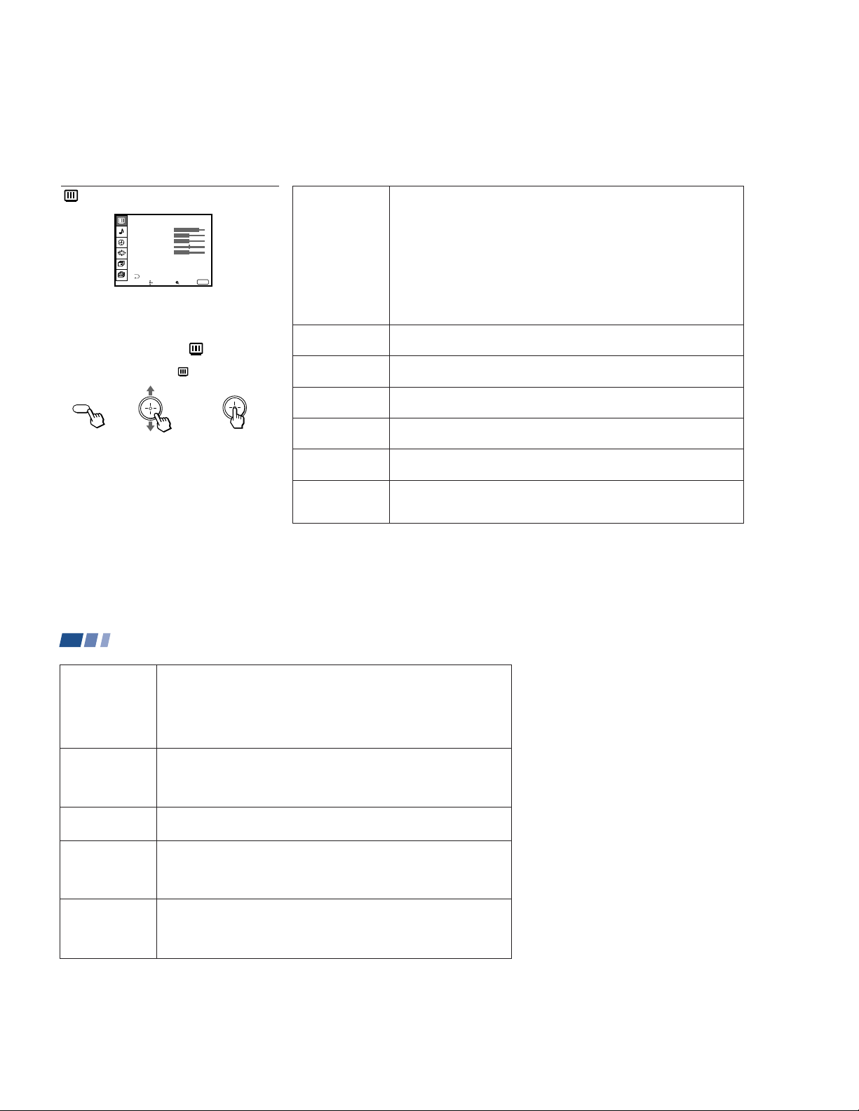
Using the VIDEO Menu
VIDEO
MODE : VIVID
PICTURE
BRIGHTNESS
COLOR
HUE
SHARPNESS
TRINITONE : HIGH
DRC MODE :
ADVANCED VIDEO
Move Select Exit
For detailed information on using the remote
control to modify menu settings, refer to
“Learning Menu Selection” on page 46.
To select the VIDEO menu:
Display / Highlight / Select
MENU
While in the VIDEO menu, move the joystick down to
scroll down to ADVANCED VIDEO to adjust additional
items, “DYNAMIC PICTURE,” “NR,” “COLOR
CORRECTION” and “DC TRANSMISSION.” (see page
48)
To restore the factory settings
Press RESET on the remote control while the
VIDEO menu is selected. To restore each
MODE to the factory setting, press RESET
after selecting the mode to be reset.
HIGH
MENU
}
Sliders
MODE
Customized picture
viewing
PICTURE
Picture Adjustment
BRIGHTNESS
Picture Adjustment
COLOR
Picture Adjustment
HUE
Picture Adjustment
SHARPNESS
Picture Adjustment
TRINITONE
White Intensity
Adjustment
You can choose one of five different video modes that best suits the program you
are watching. You can also adjust the picture quality (such as BRIGHTNESS,
COLOR, etc.) for each mode to suit your taste. First select each MODE
individually before adjusting the picture quality.
VIVID: Select for enhanced picture contrast and sharpness.
STANDARD: Select to display a standard picture for normal viewing
environments.
MOVIE: Select to display a finely detailed picture for low light environments.
GAME: Select to display graphics such as a video game.
PRO (Professional): Select to display a picture with minimum enhancements.
Press PICTURE MODE on the remote control for direct selection of a MODE
setting.
Adjust slider right (up) to increase picture contrast.
Adjust slider left (down) to decrease picture contrast.
Adjust slider right (up) to brighten the picture.
Adjust slider left (down) to darken the picture.
Adjust slider right (up) to increase color intensity.
Adjust slider left (down) to decrease color intensity.
Adjust slider right (up) to increase the green tones.
Adjust slider left (down) to increase the red tones.
Adjust slider right (up) to sharpen the picture.
Adjust slider left (down) to soften the picture.
HIGH: Select to give the white colors a blueish tint.
MEDIUM: Select to give the white colors a neutral tint.
NTSC STD: Select to give the white colors a reddish tint.
Note:
• The items, “NR,” “COLOR CORRECTION” and “DC TRANSMISSION”
are not reset to the factory settings even if you press RESET.
(continued)
47
DRC MODE
Digital Reality
Creation
DYNAMIC
PICTURE
Black Intensity
Adjustment
NR
Noise Reduction
COLOR
CORRECTION
Color Ratio
Adjustment
DC
TRANSMISSION
Black Level
Adjustment
48
Using Conventional TV Features (continued)
The DRC feature doubles both the vertical and horizontal information of the
conventional NTSC signal, allowing you to obtain a fine-detailed, realistic picture
with four-times higher density than the conventional NTSC picture.
HIGH: Use when viewing DVD, Hi8, Laser Disc, or DBS source.
LOW: Use when viewing VCR, CATV or ANT source.
GAME: Use when viewing graphics such as a video game.
Select ON to emphasize the black level and to produce a bolder dynamic picture.
Select OFF to cancel the feature.
Select ON to reduce picture noise.
Select OFF to cancel the feature.
Select ON to emphasize reds and blues.
Select OFF to reproduce skin tones.
Select ON to automatically improve the contrast ratio.
Select OFF to reproduce the black level with no compensation.
Tip
z
Since the fine-detailed DRC activated pictures contain
information four times larger than conventional pictures,
picture noise may appear. In this case, set NR to ON in
the ADVANCED VIDEO menu.
Notes:
• The following items can be adjusted for
each MODE setting (VIVID, STANDARD,
etc.) Once the adjustments are made, the
data is stored in the projection TV’s
memory and recalled whenever the
corresponding MODE setting is selected.
- PICTURE
- BRIGHTNESS
- COLOR
- HUE
- SHARPNESS
- TRINITONE
- DRC MODE
- DYNAMIC PICTURE
The “NR,” “COLOR CORRECTION,” and
“DC TRANSMISSION” settings, however,
are set independently of the MODE setting,
and remain in the ON or OFF position even
if the MODE setting is changed.
• Some shooting games which involve
pointing a light beam at the TV screen with
an electronic gun or rifle cannot be used
with this projection TV. For details, see the
instruction manual supplied with the video
game software.
– 28 –
Page 29
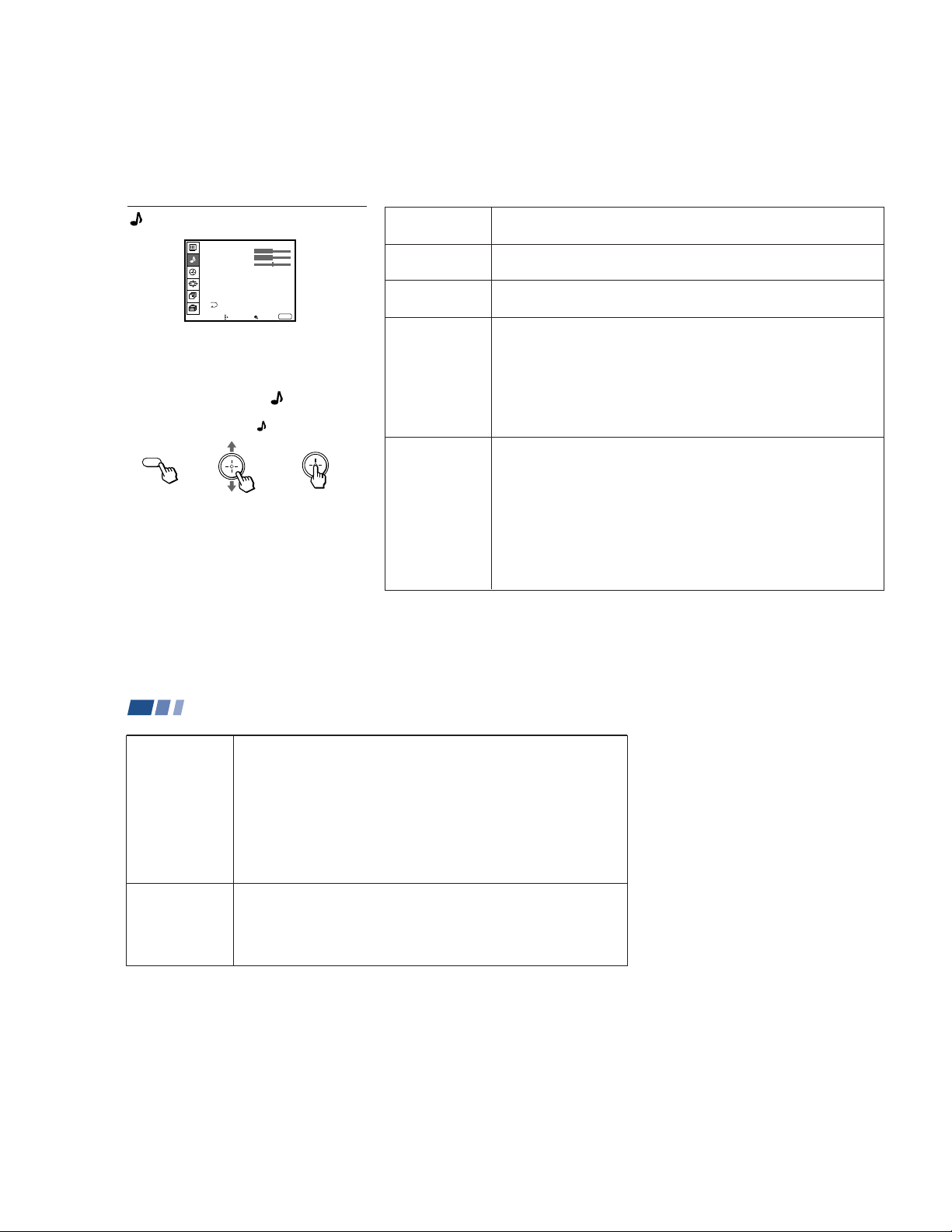
Using the AUDIO Menu
AUDIO
TREBLE
BASS
BALANCE
MTS : STEREO
SPEAKER : ALL ON
SURROUND : OFF
SURROUND LEVEL
Move Select Exit
For detailed information on using the remote
control to modify menu settings, refer to
“Learning Menu Selection” on page 46.
To select the AUDIO menu:
Display / Highlight / Select
MENU
To restore the factory settings
Press RESET on the remote control while the
AUDIO menu is selected.
MENU
Sliders
}
TREBLE
Sound Adjustment
BASS
Sound Adjustment
BALANCE
Sound Adjustment
MTS
Enjoy stereo,
bilingual and mono
programs
SPEAKER
Custom selection
of audio output
source
Adjust slider right (up) to increase high pitched sounds.
Adjust slider left (down) to decrease high pitched sounds.
Adjust slider right (up) to increase low pitched sounds.
Adjust slider left (down) to decrease low pitched sounds.
Adjust slider right (up) to emphasize right speaker volume.
Adjust slider left (down) to emphasize left speaker volume.
STEREO: Select for stereo reception when viewing a program broadcast in
stereo.
SAP: Select to listen to a bilingual broadcast. (non-SAP programs will be muted
when this feature is selected)
MONO: Select for mono reception. (use to reduce noise during stereo
broadcasts)
Quick MTS access: Press MTS on your remote control to cycle through the
MTS options as follows: (STEREO b SAP b MONO b STEREO)
ALL ON: Select to listen to the sound from the projection TV speakers alone.
L/R OFF: Select to turn off the projection TV left and right speakers and listen to
the left and right channel sounds through a separate audio system’s
speakers.
ALL OFF: Select to turn off the projection TV speakers and listen to the
projection TV’s sound only through an external audio system’s speakers.
CENTER IN: Select to use the projection TV center speaker as center speaker
when you connect an amplifier with a Dolby Pro Logic/Dolby Digital decoder.
(see “Connecting an amplifier that supports Dolby Pro Logic/Dolby
Digital decoder” on page 19)
(continued)
49
SURROUND
Customizes
surround sound
effects based on
the program’s
audio type
SURROUND
LEVEL
Speaker volume
adjustment for
surround modes
50
Using Conventional TV Features (continued)
SURROUND can only be set when SPEAKER is set to ALL ON or L/R OFF.
aa
a PRO LOGIC: Produces superb theater-like surround effects. Most effective
aa
for programs encoded in Dolby surround.
aa
a 3 STEREO: Produces a dynamic three dimensional sound without using the
aa
rear speakers. The sound of the rear channel is output from the front
speakers.
SIMULATED: Adds a surround-like effect to mono programs.
LIVE: Produces surround effects with the atmosphere of a concert hall.
GAME: Produces maximum audio impact. Most effective for video games.
OFF: Normal stereo or mono reception.
After selecting one of the surround modes, adjust the volume of each speaker
so that the sound will be even and natural. (see “Adjusting the Speaker Volume
for Customized Surround Mode” on page 51)
– 29 –
Page 30
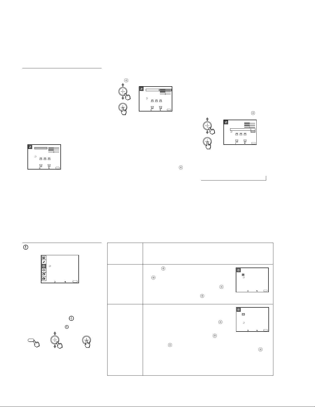
Adjusting the Speaker
Volume for Customized
Surround Mode
After you set SURROUND to one of the
modes, adjust the volume of the front, center
and rear speakers to the same level so that
the projection TV’s sound will be even and
natural. For aPRO LOGIC and a3
STEREO, adjust the speaker volume using
the test tone feature.
Adjusting the speaker volume
1 Select SURROUND LEVEL from the
AUDIO menu. (see pages 49 and 50)
aPRO-LOGIC
CENTER
REAR
BALANCE
TEST TONE : OFF
Move Select Exit
MENU
2 Move the joystick up or down to select
the speaker for volume adjustment and
press .
aPRO-LOGIC
CENTER
REAR
BALANCE
TEST TONE : OFF
Move Select Exit
MENU
CENTER: Select to adjust the level of the
center speaker. (not available for
SIMULATED)
REAR: Select to adjust the level of the rear
speakers. (not available for
a3 STEREO)
BALANCE: Select to adjust the balance
between the right and left speakers.
3 Move the joystick up, down, left or right
to adjust the volume level and press .
4 Use the joystick to select other speakers
and to adjust the volume levels.
Adjusting the speaker volume
using the test tone
The TEST TONE feature makes it easier to
adjust the volume level. You can use this
feature for aPRO LOGIC and a3 STEREO
modes only.
1 With the SURROUND LEVEL window
open, move the joystick up or down to
select TEST TONE and press
aPRO-LOGIC
CENTER
REAR
BALANCE
TEST TONE : ON
Move Select Exit
.
OFF
MENU
2 Move the joystick up or down to select
ON.
A test tone will be output from each
speaker in sequence:
Front left nCenter nFront right nRear
n
To turn off the test tone, select OFF.
3 Follow steps 2 through 4 in “Adjusting
the speaker volume.”
51
Using the TIMER Menu
TIMER
DAYLIGHT SAVING : NO
CURRENT TIME
ON / OFF TIMER
– – : – AM–
– – –
Move Select Exit
After setting the clock you can use the timer
to turn the projection TV on and off.
For detailed information on using the remote
control to modify menu settings, refer to
“Learning Menu Selection” on page 46.
To select the TIMER menu:
Display / Highlight / Select
MENU
Tip
z
Set daylight saving time before setting the clock. Any
loss of power will cause these settings to be erased.
52
MENU
DAYLIGHT
SAVING
Automatically
adjusts the time.
CURRENT
TIME
Necessary for the
TIMER.
ON/OFF TIMER
Wake up or
scheduled viewing.
Spring: Select YES to compensate for Daylight Saving Time.
The current time automatically moves ahead one hour.
Fall: Select NO at the end of Daylight Saving Time.
The current time moves back one hour.
1 Press , then move the joystick up or down until
the current day (MON-SUN) is displayed, and press
.
CURRENT TIME
––: –AM–
–––
2 Move the joystick up or down until the current hour
(01-12) and AM/PM is displayed, and press .
3 Move the joystick up or down until the current minute
Move Select
Exit
(00-59) is displayed, and press .
The Clock has now started. Press MENU to exit.
1 Select the desired timer (1 or 2).
2 Move the joystick up or down until the desired day
(MON-SUN) or range of days (EVERY SUN-SAT or
EVERY MON-FRI) is displayed, and press .
3 Move the joystick up or down until the time (hours
and minutes) that you want the projection TV to
ON / OFF TIMER
1.
––––––
––: ––AM–Hch
2.
––––
––: ––AM–Hch
SUN
12: 0AM0
Move Select
Exit
remain on is displayed, and then press .
4 Move the joystick up or down to set the time duration (maximum of 6 hours)
and press .
5 Move the joystick up or down to select the desired channel and press .
The timer is now set. The TIMER/STAND BY indicator on your projection TV
will be lit.
Press MENU to exit.
RESET while in the ON/OFF TIMER window.
To cancel your timer setting, select timer 1 or 2 and press
Performing AUTO PROGRAM will
erase all TIMER settings.
MENU
–––
–––
MENU
– 30 –
Page 31

Using the WIDE SCREEN
CHANNEL SKIP/ADD
Select a channel
2 :
3 :
4 :
5 :
6 :
7 :
8 :
NO
1 :
Move Select Exit
MENU
NO
NO
NO
NO
NO
NO
NO
MODE Menu
WIDE SCREEN MODE
AUTO WIDE : ON
WIDE MODE : NORMAL
V CENTER : 0
Move Select Exit
For detailed information on using the remote
control to modify menu settings, refer to
“Learning Menu Selection” on page 46.
To select the WIDE SCREEN MODE
Menu:
Display / Highlight / Select
MENU
To restore the factory settings
Press RESET on the remote control while the
WIDE SCREEN MODE menu is selected.
MENU
AUTO WIDE
Automatically
selects the wide
screen mode
WIDE MODE
Manually selects
the wide screen
mode
V CENTER
Adjusts the
position of the
picture
Select ON to automatically display the picture with an ID-1 or S1 (aspect ratio
recorded) signal in an optimum wide screen mode; normal 4:3 picture in
NORMAL, letterbox picture in ZOOM, and 4:3 squeezed picture in FULL.
Select OFF if you want to choose the wide screen mode manually by pressing
the WIDE MODE button.
You can select NORMAL, WIDE ZOOM, ZOOM or FULL for the 4:3 or
letterbox picture to fill the 16:9 screen manually by pressing the WIDE MODE
button. (for details on each mode, see “Using the Wide Screen Mode” on page
39)
Allows you to move the picture vertically within the screen (available only in
ZOOM and WIDE ZOOM modes).
Move the joystick up or down to move the picture, and press .
53
Using Conventional TV Features (continued)
Using the CHANNEL SET
UP Menu
CHANNEL SET UP
CABLE : ON
AUTO PROGRAM
CHANNEL SKIP/ADD
CHANNEL CAPTION
FAVORITE CHANNEL : AUTO
CHANNEL FIX : OFF
Move Select Exit
For detailed information on using the remote
control to modify menu settings, refer to
“Learning Menu Selection” on page 46.
To select the CHANNEL SET UP
menu:
Display / Highlight / Select
MENU
54
MENU
CABLE
Cable system
setting
AUTO
PROGRAM
Automatic
channel presetting
CHANNEL
SKIP/ADD
Skips unnecessary
channels
Select ON if your projection TV is connected to a cable system.
Select OFF if your projection TV is connected to an antenna.
AUTO SET UP will set CABLE to OFF automatically if a cable channel is not
available.
Select YES to signal the projection TV to automatically program all receivable
conventional TV channels. When all the receivable channels are stored, the
lowest numbered channel is displayed.
Select NO to cancel AUTO PROGRAM.
After AUTO SET UP, you can erase unnecessary
conventional TV channels from the channel preset
memory.
With the CHANNEL SKIP/ADD window open:
1 Move the joystick up or down to select the desired
channel. You can view the channel that is selected
with the CHANNEL SKIP/ADD menu in the center
sub screen. You can also use CH +/– or 0–9 and
ENTER buttons.
2 Press .
3 Move the joystick up or down to select YES, and press .
The selected channel will be erased.
If you want to re-enter the skipped channel, follow the steps above and select
NO.
(continued)
– 31 –
Page 32

CHANNEL
CAPTION
Easy recognition
of the channel
you are watching
FAVORITE
CHANNEL
User’s favorite
channels
You can add a caption for up to 32 channels of both
VHF/UHF and AUX inputs.
With the CHANNEL CAPTION window open:
CHANNEL CAPTION
CHANNEL : – – –
CAPTION : – –––
1 Press and then move the joystick up or down to
select the desired channel. You can view the channel
that is selected with the CHANNEL CAPTION menu
Move Select
MENU
Exit
in the center sub screen.
2 Press .
3 Move the joystick up or down to display the first letter
or number of the caption and press to select it.
Repeat until up to four digits are selected.
4 Press .
To erase a caption, press RESET.
The FAVORITE CHANNEL feature enables easy access to the eight channels that
you preset (or the last channel that you were watching).
(for details on how to set up this feature, see "Setting and Selecting FAVORITE
CHANNEL" on page 57)
(continued)
55
CHANNEL FIX
Locks selection of
your projection
TV’s input when
used in conjunction
with external
equipment such as
a cable box, AV
receiver, etc.
56
Using Conventional TV Features (continued)
2-6: When the cable box is connected to the VHF/UHF input, you can fix the TV’s
input to one of the channels between 2 and 6. Press DBS/CABLE (FUNCTION)
and then CH +/– to change the cable box channels.
AUX 2-6: Use this when a cable box is connected to AUX, and a cable or antenna
is connected to VHF/UHF.
VIDEO 1: Use this when you have connected external video equipment (e.g. AV
receiver) and you want the projection TV’s input fixed to it.
OFF: When you want to switch CHANNEL FIX off.
If the projection TV is in the AUX mode when you turn CHANNEL FIX off, press
ANT to return to UHF input mode.
TIMER settings are erased when CHANNEL FIX is set. (If ANT2-6 or AUX2-6
is selected, timer settings for those channels are not erased)
Note:
• You cannot change channels with the TV’s
tuner when you set CHANNEL FIX. If
you want to use the TV’s tuner while
fixing the TV’s input to VIDEO 1, use the
SET UP menu to set SELECT OUT to TV
OUT. (see “SELECT OUT” on page 60)
– 32 –
Page 33

Setting and Selecting FAVORITE CHANNEL
FAVORITE CHANNEL
Select a position
2 .
3 .
4 .
5 .
6 .
7 .
8 .
1 .
2
10
22
30
40
52
125
1
SPTN
CNN
Move Select Exit
MENU
FAVORITE CHANNEL
Select a channel
2 .
3 .
4 .
5 .
6 .
7 .
8 .
1 .
2
10
22
30
40
52
125
SPTN
1 CNN
Move Select Exit
MENU
FAVORITE CHANNEL
Select a channel
2 .
3 .
4 .
5 .
6 .
7 .
8 .
Move Select Exit
MENU
1 .
125
10
22
30
40
52
125
SPTN
1 CNN
The FAVORITE CHANNEL feature of your
projection TV enables easy access to the eight
channels that you preset (or the last channel
that you were watching).
Your FAVORITE CHANNEL options can be
set automatically or manually.
The factory setting for FAVORITE
CHANNEL is AUTO.
When FAVORITE CHANNEL is set to
AUTO, the last eight channels selected with
the 0–9 buttons will be set as FAVORITE
CHANNEL options. If you want to input
your own selections as FAVORITE
CHANNEL settings, set to MANUAL.
Setting FAVORITE CHANNEL
manually
1 Select FAVORITE CHANNEL from the
CHANNEL SET UP menu. (see pages 54
and 55)
CHANNEL SET UP
CABLE : ON
AUTO PROGRAM
CHANNEL SKIP/ADD
CHANNEL CAPTION
FAVORITE CHANNEL : AUTO
CHANNEL FIX :
Move Select Exit
MANUAL
MENU
2 Move the joystick up or down to select
MANUAL and press .
The FAVORITE CHANNEL menu will
appear. If you set CHANNEL CAPTION
names (e.g. CNN, HBO), they will also be
displayed. (see “CHANNEL CAPTION”
on page 55)
3 Move the joystick up or down to select a
position (1–8), and press .
4 Move the joystick up or down to select a
channel.
You have now selected a favorite channel.
5 Press and use the joystick to program
other favorite channels. (Follow steps 3
and 4.)
6 Press MENU when you have finished.
Your favorite channels are now ready for
use.
(continued)
57
Using Conventional TV Features (continued)
Resetting FAVORITE CHANNEL
choices
You have the option of returning to the
FAVORITE CHANNEL screen to adjust any
of your favorite channel choices.
Simply proceed as described in “Setting
FAVORITE CHANNEL manually” (skip step
2 if MANUAL is already selected).
When you reach step 3, select the position
you want to change and press
RESET to clear the channel for that position.
FAVORITE CHANNEL
___
1 .
2 .
2
SPTN
3 .
10
4 .
22
5 .
30
6 .
40
7 .
52
8 .
125
Select a channel
Move Select Exit
Move the joystick up or down to select a new
channel.
Press MENU when you are done.
Note:
• The FAVORITE CHANNEL feature is not
available for the picture input from AUX
or VIDEO 5 IN, and for digital TV
programs.
58
. Press
MENU
Using FAVORITE CHANNEL
You can use the FAVORITE CHANNEL
feature to directly select the channel you want
to watch.
1 Press once.
The favorite channel menu and a window
picture will be superimposed over the
current channel. The window picture
displays the channel selected from the
menu.
FAVORITES
12 CNN
36 ESPN
50
60
70
80
90
120 MTV
EXIT
2 Move the joystick up or down to select the
channel that you wish to view from the
menu.
The picture of the selected channel will be
displayed in the window picture.
FAVORITES
12 CNN
36 ESPN
50
60
70
80
90
120 MTV
EXIT
– 33 –
3 Press to select the channel.
The selected channel will be displayed for
normal viewing.
To cancel the favorite channel menu before
selecting a channel, move the joystick up or
down to select EXIT at the bottom of the
menu and press
.
Page 34

Using the SET UP Menu
FREEZE MODE:
Move Select Exit
MENU
SET UP
PARENTAL CONTROL
CAPTION VISION:
LANGUAGE:
SELECT OUT:
VIDEO LABEL
DIRECT PLAY
CC1
VIDEO1
MONITOR
VIDEO2
VIDEO3
VIDEO4
TV OUT
Set up using YES
only VIDEO1 input? NO
SET UP
PARENTAL CONTROL
CAPTION VISION:
SELECT OUT: MONITOR
LANGUAGE: ENGLISH
VIDEO LABEL
DIRECT PLAY
FREEZE MODE: NORMAL
Move Select Exit
CC1
MENU
For detailed information on using the remote
control to modify menu settings, refer to
“Learning Menu Selection” on page 46.
To select the SET UP menu:
Display / Highlight / Select
MENU
Notes:
• When you set SELECT OUT to TV OUT,
you cannot swap the main/right and
window/left pictures.
• The SELECT OUT signal is only available
when the projection TV is on.
PARENTAL
CONTROL
Blocks programs
unsuitable for children
CAPTION VISION
Television closed
caption display
Allows you to block TV programs that you feel are unsuitable for your children.
(see “Using the PARENTAL CONTROL Feature” on page 64 for details)
PARENTAL LOCK: Select ON to activate PARENTAL CONTROL. Programs
that match the selected ratings will be blocked.
Select OFF to turn off PARENTAL CONTROL. You can view all programs.
RATING: Select to choose from three Sony’s predetermined modes and one
custom rating mode (CHILD/YOUTH/YOUNG ADULT and CUSTOM)
PASSWORD: Select to change the password.
Some programs are broadcast with Caption Vision.
To display Caption Vision, select CC 1, CC 2, CC 3,
CC 4, TEXT1, TEXT2, TEXT3 or TEXT4 from the
menu. Then press the CC button until Caption Vision
is displayed.
CC 1, CC 2, CC 3 or CC 4 displays a printed
SET UP
PARENTAL CONTROL
CAPTION VISION
SELECT OUT:MONITOR
LANGUAGE:ENGLISH
VIDEO LABEL
DIRECT PLAY
FREEZE MODE:NORNAL
Move Select Exit
TEXT1
TEXT2
TEXT3
TEXT4
CC1
CC2
CC3
CC4
MENU
version of the dialogue or sound effects of a
program. (The mode should be set to CC 1 for most
programs.) TEXT1, TEXT2, TEXT3, or TEXT4
displays network/station information presented using
either half or the whole screen.
Notes:
• Poor reception of conventional TV programs can cause errors in Caption
Vision and XDS.
Captions may appear with a white box or other errors instead of the intended
text.
• XDS, Caption Vision, and the status display cannot be used at the same time.
(continued)
59
60
SELECT OUT
Output signal
selection from
SELECT OUT
Using Conventional TV Features (continued)
– 34 –
SET UP
PARENTAL CONTROL
CAPTION VISION:
SELECT OUT:
LANGUAGE:
VIDEO LABEL
DIRECT PLAY
FREEZE MODE:
Move Select
You can select the desired output signal from the
SELECT OUT jacks on the upper panel at the rear.
MONITOR: Select to edit tapes while monitoring.
SELECTOUT outputs the picture displayed on the
screen.
Note:
• With this setting, the picture input from VIDEO 5
IN or digital TV programs is not output from
SELECT OUT.
VIDEO1–VIDEO4: Select to edit tapes while viewing an input image different
from that being recorded. SELECT OUT outputs the signal input to the
projection TV regardless of the displayed picture on the screen.
TV OUT: Select if you connect an AV receiver to VIDEO 1 IN. SELECT OUT
outputs the signal that the TV is tuned to, regardless of the displayed picture.
(see “Connecting an AV receiver” on page 17 for connection)
If you select TV OUT, the following pop-up menu appears.
Note:
• With this setting, digital TV signal is not output
from SELECT OUT.
Select YES only if you have connected an AV
receiver, with no other equipment, to your projection
TV. You can always select the signal from the
receiver by pressing TV/VIDEO once.
Note:
• If you select YES, you cannot view a digital TV program as SELECT OUT
does not output a digital TV signal to the receiver.
Select NO if you have connected multiple components to your projection TV.
You can select an input (VIDEO1 – VIDEO4) with the TV/VIDEO button.
MONITOR
VIDEO1
VIDEO2
VIDEO3
VIDEO4
TV OUT
Exit
CC1
MENU
Page 35

LANGUAGE
User’s preferred
language
VIDEO LABEL
Easy recognition of
connected
equipment
(e.g. DBS, VHS,
etc.).
Select from available languages (English or Spanish) to display all menus in
your language of choice.
This feature allows you to label each input mode so
that you can easily identify the connected equipment
(e.g. you can label VIDEO 1 IN as VHS).
VIDEO LABEL
VIDEO1:
VIDEO2:
VIDEO3:
VIDEO4:
VIDEO1
VIDEO2
VIDEO3
VIDEO4
With the VIDEO LABEL window open:
1 Move the joystick up or down to select the input
mode you want to label and press .
VIDEO LABEL
VIDEO1:
VIDEO2:
VIDEO3:
VIDEO4:
Move Select Exit
VIDEO1
BETA
AV RECEIVER
VHS
8mm
DBS
DVD
SKIP
LD
MENU
Move Select Exit
MENU
2 Move the joystick up or down to select the label and
press .
VIDEO LABEL Options:
VIDEO 1: VIDEO 1, VHS, 8mm, BETA, LD, DBS, DVD, AV RECEIVER,
SKIP
VIDEO 2–4: VIDEO 2–4, VHS, 8mm, BETA, LD, DBS, DVD, SKIP
If you select SKIP, your projection TV will skip this connection when you scan
through video sources using the TV/VIDEO button.
(continued)
61
DIRECT PLAY
Easy operation of a
connected VCR
62
Using Conventional TV Features (continued)
This feature allows you to switch the input mode from
the TV to a Sony VCR (MDP or DVD) and start
playing by only pressing the ( (playback) button on
the remote control. You have to set the VTR 1/2/3/
DVD/MDP switch on the remote control (e.g., you
connect your VCR to the VIDEO 3 IN jacks and set
the VTR 1/2/3/DVD/MDP switch to VTR 1).
With the DIRECT PLAY window open:
1 Move the joystick up or down to select the input to which your video
equipment is connected, and press .
DIRECT PLAY
VIDEO1:
VIDEO2:
VIDEO3:
VIDEO4:
1 2 3 DVD/MDP
Move Select Exit
VTR1
VTR2
VTR3
DVD/MDP
OFF
MENU
2 Move the joystick up or down to select the position of the VTR 1/2/3/DVD/
MDP switch, and press .
DIRECT PLAY
VIDEO1:
VIDEO2:
VIDEO3:
VIDEO4:
1 2 3 DVD/MDP
Move Select Exit
(continued)
OFF
OFF
OFF
OFF
MENU
– 35 –
Page 36

FREEZE MODE
Freeze picture
mode
Useful when you need to copy down information that appears on the TV’s
screen.
Note: The FREEZE MODE feature is not available for the inputs from VIDEO
5 IN and for digital TV programs.
NORMAL: Select to freeze the whole picture on the screen by pressing
FREEZE.
Recipe
flour - - - - 2
sugar - - - 1/2
salt - - - - - 1/2
butter - - - 1
The current picture freezes.
TWIN: Select to freeze the desired scene and display it on the left of the
screen while viewing the normal picture of the current channel on
the right by pressing FREEZE.
This mode is not available for PIP, P&P or CH INDEX screens.
Frozen picture
Recipe
flour - - - - 2
sugar - - - 1/2
salt - - - - - 1/2
butter - - - 1
Normal motion picture
66
Press FREEZE again or press (OFF) to display the normal picture.
63
Using Conventional TV Features (continued)
Using the PARENTAL
CONTROL Feature
TV programs and movies shown on TV are
given a rating signal based on one of two
rating systems. One is the Television Parental
Guidelines to rate television programs (TV
ratings), and the other is the Motion Picture
Association of America (MPAA) Guidelines
to rate movies including those shown on TV
(movie ratings).
To block programs you feel are unsuitable for
your children, you need to set the TV for
both rating systems. Sony’s predetermined
ratings are also available.
See pages 70 and 71 for a description of the
ratings.
Activating the PARENTAL
CONTROL Feature
First, set a password, then select your desired
rating from Sony’s predetermined ratings.
1 Select PARENTAL CONTROL from the
SET UP menu. (see page 59)
SET UP
PARENTAL CONTROL
CAPTION VISION:
SET NEW
SELECT OUT:
PASSWORD
LANGUAGE:ENGLISH
___
_
VIDEO LABEL
DIRECT PLAY
FREEZE MODE:NORMAL
Use [0-9] to enter
64
password
Move Exit
MENU
2 Enter a four digit password using the 0–9
buttons.
SET UP
PARENTAL CONTROL
CAPTION VISION:
CONFIRM
SELECT OUT:
PASSWORD
LANGUAGE:ENGLISH
___
_
VIDEO LABEL
DIRECT PLAY
FREEZE MODE:NORMAL
Comfirm password
Move Exit
MENU
3 To confirm the password, re-enter the
same password with the 0–9 buttons.
Your password is stored and the
PARENTAL CONTROL menu
automatically appears.
If you want to change the password, see
page 69.
PARENTAL CONTROL
PARENTAL LOCK:
RATING: CHILD
CHANGE PASSWORD
Move Select Exit
OFF
MENU
4 Make sure that PARENTAL LOCK is
highlighted, and press .
PARENTAL CONTROL
PARENTAL LOCK:
RATING: CHILD
CHANGE PASSWORD
Move Select Exit
ON
OFF
MENU
5 Move the joystick up or down to select
ON, and press .
PARENTAL CONTROL
PARENTAL LOCK:
RATING: CHILD
CHANGE PASSWORD
Move Select Exit
ON
MENU
6 Move the joystick up or down to select
RATING, and press .
PARENTAL CONTROL
RATING:
CHANGE PASSWORD
Age up to 6
Move
CHILD
YOUTH
YOUNG ADULT
CUSTOM
Select Exit
ONPARENTAL LOCK:
MENU
7 Move the joystick up or down to select a
desired rating (CHILD, YOUTH and
YOUNG ADULT), and press
If you want to select the ratings from
CUSTOM, go to step 4 of “Selecting a
Custom Rating” on page 66.
.
8 Press MENU to exit the menu.
– 36 –
Page 37

To deactivate the PARENTAL CONTROL
Move Exit
MENU
SET UP
CAPTION VISION:
Use [0-9] to enter
password
SELECT OUT:
LANGUAGE:ENGLISH
VIDEO LABEL
DIRECT PLAY
PASSWORD
_
FREEZE MODE:NORMAL
PARENTAL CONTROL
___
Move Exit
MENU
SET UP
CAPTION VISION:
Use [0-9] to enter
password
SELECT OUT:
LANGUAGE:ENGLISH
VIDEO LABEL
DIRECT PLAY
PASSWORD
_
FREEZE MODE:NORMAL
PARENTAL CONTROL
___
TV RATING
Move
Select rating
Select Exit
MENU
TV–Y
TV–Y7
TV–G
TV–PG
TV–14
TV–MA
_
_ :FV _
_
_ :D _ L _ S _ V _
_ :D _ L _ S _ V _
_ : L _ S _ V _
TV RATING
Move
Allow rating
Select Exit
MENU
TV–Y
TV–Y7
TV–G
TV–PG
TV–14
TV–MA
_
_ :FV _
_
:D _ L _ S _ V _
_ :D _ L _ S _ V _
: L _ S _ V _
_
feature
If you set PARENTAL LOCK in the
PARENTAL CONTROL menu to OFF, the
PARENTAL CONTROL feature will be
canceled and you can view all TV programs
and movies shown on TV.
1 Select PARENTAL CONTROL from the
SET UP menu. (see page 59)
3 Move the joystick up or down to select
PARENTAL LOCK, and press
PARENTAL CONTROL
PARENTAL LOCK:
RATING: CHILD
CHANGE PASSWORD
Move Select Exit
ON
OFF
MENU
.
4 Move the joystick up or down to select
OFF, and press .
PARENTAL CONTROL
PARENTAL LOCK:
RATING: CHILD
CHANGE PASSWORD
OFF
To deactivate the PARENTAL CONTROL
feature for the current program
When you select a PARENTAL CONTROL
program, no sound or picture except for a
channel number will appear. The
indicator
is displayed. To view the program, follow the
steps below.
1 Press ENTER to display the “Password”
screen.
2 Enter your password using the 0–9
buttons. Parental control will be canceled
(PARENTAL LOCK set to OFF) until you
turn your projection TV off.
2 Enter your four digit password using the
0–9 buttons.
PARENTAL CONTROL
PARENTAL LOCK:
RATING: CHILD
CHANGE PASSWORD
Move Select Exit
ON
MENU
Using Conventional TV Features (continued)
Selecting a Custom Rating
If you want to select the ratings to be blocked
from CUSTOM once you have activated the
PARENTAL CONTROL feature (page 64),
follow the procedure below.
For a detailed description of each rating, see
“What the Ratings Mean” on pages 70 and
71.
1 Select PARENTAL CONTROL from the
SET UP menu. (see page 59)
Move Select Exit
MENU
5 Press MENU to exit the menu.
3 Move the joystick up or down to select
RATING, and press
.
PARENTAL CONTROL
RATING:
YOUTH
CHANGE PASSWORD
YOUNG ADULT
CUSTOM
Age up to 6
Move
Select Exit
CHILD
ONPARENTAL LOCK:
MENU
4 Move the joystick up or down to select
CUSTOM, and press .
CUSTOM RATING
TV RATING
MOVIE RATING
UNRATED: VIEW ALL
(continued)
65
First, select a TV rating.
5 Move the joystick up or down to select
TV RATING, and press .
6 Move the joystick up or down to select
the TV rating to be blocked, and press
.
2 Enter your four digit password using the
0–9 buttons.
The PARENTAL CONTROL menu
appears.
PARENTAL CONTROL
PARENTAL LOCK:
RATING: CHILD
CHANGE PASSWORD
Move Select Exit
66
ON
MENU
Select category
Move
– 37 –
Select Exit
MENU
Page 38

7 Move the joystick up or down to select
CUSTOM RATING
Move
Select category
Select Exit
MENU
TV RATING
MOVIE RATING
UNRATED: VIEW ALL
MOVIE RATING
Move
Select rating
Select Exit
MENU
G
PG
PG–13
R
NC–17
X
–
–
–
–
–
–
CUSTOM RATING
Move Select Exit
MENU
TV RATING
MOVIE RATING
UNRATED: BOTH
Block all unrated
programming
, and press .
The indicator automatically appears
beside the selected rating and all “higher”
ratings, indicating that the programs that
match the ratings will be blocked.
TV RATING
_
TV–Y
_ :FV _
TV–Y7
_
TV–G
– :D – L – S – V –
TV–PG
– :D – L – S – V –
TV–14
– : L – S – V
TV–MA
Select category
Move
Some ratings have additional content
ratings called “extenders.” The extenders
are defined as follows: D (sexually
suggestive Dialog), FV (Fantasy
Violence), L (coarse Language), S (Sexual
situations) and V (Violence). By setting
the extenders, you can define additional
viewing limits. For more details of
extenders, see page 71.
All of the extenders included in the
selected ratings will be blocked. If you
wish to allow any of them to be viewed,
go to step 8.
Select Exit
MENU
8 Move the joystick left or right to select
the extender to be viewed, and press
TV RATING
_
TV–Y
_ :FV _
TV–Y7
_
TV–G
– :D – L – S – V –
TV–PG
– :D – L – S – V –
TV–14
– : L – S – V
TV–MA
Block content
Move
Select Exit
MENU
9 Move the joystick up or down to select
“–,” and press .
“–” appears beside the selected extender,
indicating that the programs that match
the extender can be viewed.
If you select
that the programs that match the
extender will be blocked again.
, is displayed to show
TV RATING
_
TV–Y
_ :FV _
TV–Y7
_
TV–G
– :D – L – S – V _
TV–PG
– :D – L – S – V –
TV–14
– : L – S – V
TV–MA
Select category
Move
Select Exit
MENU
10
Repeat steps 8 and 9 for other extenders.
.
All programs that match the ratings you
select and higher, except for the
extenders that were canceled, will be
blocked.
11
After setting of the TV rating is complete,
move the joystick up or down to select
, and press .
Second, select a movie rating.
12
Move the joystick up or down to select
MOVIE RATING, and press
.
(continued)
67
13
14
15
68
Using Conventional TV Features (continued)
Move the joystick up or down to select
the movie rating to be blocked, and press
.
MOVIE RATING
–
G
–
PG
–
PG–13
–
R
–
NC–17
–
X
Block rating
Move
Move the joystick up or down to select
, and press .
The
indicator automatically appears
beside the selected rating and all “higher”
ratings, indicating that the programs that
match the ratings will be blocked.
MOVIE RATING
G
PG
PG–13
R
NC–17
X
Select rating
Move
Press MENU to exit the menu.
Select Exit
–
–
–
–
–
–
Select Exit
MENU
MENU
To block TV programs and/or movies
for which a rating signal is not given
(NR and N/A)
For a description of the NR and N/A ratings,
see pages 70 and 71.
1 Perform steps 1–4 of “Selecting a Custom
Rating” on page 66.
2 Move the joystick up or down to select
Select Exit
.
MENU
UNRATED, and press
CUSTOM RATING
TV RATING
MOVIE RATING
UNRATED: VIEW ALL
TV
MOVIE
BOTH
No block
Move
– 38 –
3 Move the joystick up or down to select
the type of programs to be blocked, and
press
.
If you select VIEW ALL, you can view
any TV program and movie that are
unrated. If you select BOTH, all of the TV
programs and movies unrated will be
blocked.
4 Press MENU to exit the menu.
Page 39
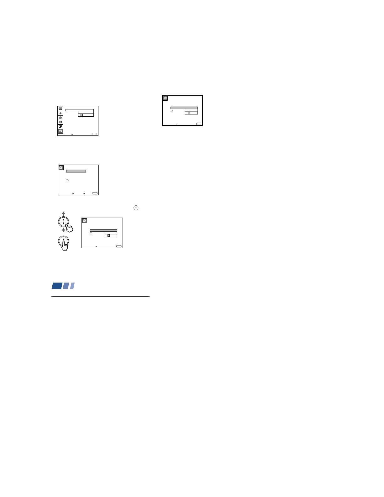
Changing the Password
Move Exit
MENU
SET UP
CAPTION VISION:
Use [0-9] to enter
password
SELECT OUT:
LANGUAGE:ENGLISH
VIDEO LABEL
DIRECT PLAY
PASSWORD
_
FREEZE MODE:NORMAL
PARENTAL CONTROL
___
1 Select PARENTAL CONTROL from the
SET UP menu. (see page 59)
2 Enter your four digit password using the
0–9 buttons.
The PARENTAL CONTROL menu
appears.
PARENTAL CONTROL
PARENTAL LOCK:
RATING: CHILD
CHANGE PASSWORD
ON
4 Enter a new four digit password using
the 0–9 buttons.
PARENTAL CONTROL
PARENTAL LOCK: ON
RATING:
CHANGE PASSWORD
Confirm password
Move Exit
CHILD
COMFIRM
____
MENU
5 Enter the password set in step 4 again to
confirm.
If you entered it incorrectly, “Password
incorrect” appears.
Re-enter the correct password.
6 Press MENU to exit the menu.
If you have forgotten your password
In step 2 of “Changing the Password” above,
enter the master password “4353”
(corresponding to “HELP” on a phone
number pad). You can then store a new
password.
(continued)
Move Select Exit
MENU
3 Move the joystick up or down to select
CHANGE PASSWORD, and press
PARENTAL CONTROL
PARENTAL LOCK: ON
RATING:
CHANGE PASSWORD
Use [0-9] to enter
new four digit
password
Move Exit
NEW
CHILD
____
MENU
.
Using Conventional TV Features (continued)
What the Ratings Mean
Sony’s predetermined ratings
These are original ratings that Sony
predetermined according to the viewer’s age.
Each rating allows you to view the certain
programs, as follows.
See pages 70 and 71 for a description of TV
and movie ratings.
CHILD: Suitable for children under the age
of 6.
Viewable movie ratings: G, NR, and N/A
Viewable TV ratings: TV-Y, TV-G, and TV-NR
YOUTH: Suitable for children aged 7 and
older.
Viewable movie ratings: G, PG, NR, and N/A
Viewable TV ratings: TV-Y, TV-Y7, TV-G, TVPG, and TV-NR
YOUNG ADULT: Suitable for children aged
14 and older.
Viewable movie ratings: G, PG, PG-13, NR,
and N/A
Viewable TV ratings: TV-Y, TV-Y7, TV-G, TVPG, TV-14, and TV-NR
Movie ratings
Movie ratings are for movies (including those
shown on TV) rated according to the Motion
Picture Association of America (MPAA)
Guidelines.
G (General Audiences—All Ages
Admitted): In G-rated films no strong words
are used, the violence is at a minimum,
nudity and sex scenes are not present, nor is
there any drug use.
PG (Parental Guidance Suggested. Some
Material May Not Be Suitable For
Children): This is a film which may need to
be monitored first by parents.
PG-13 (Parents Strongly Cautioned. Some
Material May Be Inappropriate For Children
Under 13): Parents are alerted to be very
careful about the attendance of their underteenage children when viewing.
R (Restricted, Under 17 Require
Accompanying Parent Or Adult Guardian):
This film includes hard language, tough
violence, nudity, drug abuse or other
elements of concern.
69
NC-17 or X (No One 17 Or Under
Admitted.): This is a film that most parents
would consider not suitable for children
aged 17 and under. There may be violence,
sex, abberrational behavior, drug abuse or
other elements of concern.
NR (Not Rated): This is a film that a
producer has not rated, intending to have his
film widely released.
N/A (Not Applicable): This is a film that a
producer considers outside the scope of the
MPAA ratings.
Note:
• NR and N/A ratings are shown together
as UNRATED in the menu.
70
– 39 –
Page 40

TV ratings
TV ratings are for TV programs rated
according to the Television Parental
Guidelines.
TV-Y (All Children): This program is
designed for young children aged 2–6 and is
appropriate for all children.
TV-Y7 (Directed to Older Children): This
program is designed for children aged 7 and
above. Themes and elements in this program
may include mild fantasy violence or
slapstick violence, or may frighten children
under the age of 7.
TV-G (General Audience): Most parents
would find this program suitable for all ages.
It contains little or no violence, no strong
language and little or no sexual dialog or
situations.
TV-PG (Parental Guidance Suggested):
This program contains some material that
parents may find unsuitable for younger
children.
TV-14 (Parents Strongly Cautioned): This
program contains some material that many
parents would find unsuitable for children
under the age of 14.
TV-MA (Mature Audience Only): This
program is specifically designed to be
viewed by adults and therefore may be
unsuitable for children under the age of 17.
TV-NR (Not Rated/Unrated): This is a
program broadcast without any rating, such
as news, news flashes or sports.
This setting is shown as UNRATED in the
menu.
Note:
TV-Y7, TV-PG, TV-14 and TV-MA ratings
have additional content ratings called
“extenders” to define additional viewing
limits. The extenders are defined as follows:
D (sexually suggestive Dialog): Programs
containing suggestive dialog, or sexual
innuendo
FV (Fantasy Violence): Programs containing
cartoon violence occurring in TV-Y7
programs only
L (coarse Language): Programs containing
coarse language
S (Sexual situations): Programs containing
sexual content
V (Violence): Programs containing violence
There may be some profanity, violence or
brief nudity in these programs.
71
Operating Video Equipment
Setting the Manufacturer's
Code
You can use the supplied remote control to
operate Sony or non-Sony video equipment
that has an infrared sensor.
1 Set the VTR 1/2/3/DVD/MDP switch to
the input through which you would like
to access your video equipment.
The following Sony equipment is preset to
each input as shown below:
VTR1 (303) Beta, ED Beta VCRs
VTR2 (302) 8 mm VCR
VTR3 (301) VHS VCR
DVD/MDP (751) DVD Player
2 Press CODE SET, DVD/VTR (FUNCTION),
and the 0-9 buttons to enter the
manufacturer’s code number (see the
following chart), then press ENTER.
For example, to operate a Sony 8mm VCR:
FUNCTION
CODE SET
DVD/VTR
3
0
If the remote control doesn’t work
• See the note on page 73.
72
ENTER
2
VCR manufacturer code numbers
Manufacturer Code
Sony 301, 302, 303
Aiwa 338
Admiral (M. Ward) 327
Audio Dynamic 314, 337
Bell & Howell (M. Ward) 330, 343
Broksonic 319, 317
Canon 309, 308
Citizen 332
Craig 315, 302, 332
Criterion 315
Curtis Mathis 304, 338, 309
Daewoo 341, 312, 309
DBX 314, 336, 337
Dimensia 304
Emerson 319, 320, 316, 317, 318, 341
Fisher 330, 334, 335, 333
Funai 338
General Electric 329, 304, 309
Go Video 340, 339, 322
Goldstar 332
Hitachi 306, 304, 305, 338
Instant Replay 309, 308
JC Penney 309, 305, 304, 330, 314, 336, 337
JVC 314, 336, 337
Kenwood 314, 336, 332, 337
LXI (Sears) 332, 305, 333, 334, 330, 335, 338
Magnavox 308, 309, 310
Marantz 314, 336, 337
Marta 332
Memorex 309, 335
Minolta 305, 304
Mitsubishi/MGA 323, 324, 325, 326
Multitech 325, 338, 321
NEC 314, 336, 337
Olympic 309, 308
Optimus 327
Panasonic 308, 309, 306, 307
Pentax 305, 304
Philco 308, 309
Philips 308, 309, 310
Pioneer 308
Quasar 308, 309, 306
RCA/PROSCAN 304, 305, 308, 309, 311,
Realistic 309, 330, 328, 335, 324, 338
Sansui 314
Singer 315
Samsung 322, 313, 321
Sanyo 330, 335
Scott 312, 313, 321, 335, 323, 324, 325, 326
Sharp 327, 328
Shintom 315
Signature 2000 (M. Ward) 338, 327
Sylvania 308, 309, 338, 310
Symphonic 338
SV2000 338
Tashiro 332
Tatung 314, 336, 337
Teac 314, 336, 338, 337
Technics 309, 308
Teknica 342, 338
Toshiba 312, 311
Wards 327, 328, 335, 331, 332
XR-1000 315
Yamaha 330, 314, 336, 337
Zenith 331
329, 312, 313, 310
– 40 –
Page 41

MDP manufacturer code numbers
Manufacturer Code
Sony 701
Panasonic 704
Pioneer 702
DVD Player manufacturer code
numbers
Manufacturer Code
Sony 751
Panasonic 753
Pioneer 752
RCA 755
Toshiba 754
Tips
z
• In some rare cases, you may not be able to operate your
non-Sony video equipment with the supplied remote
control. In this case, please use the equipment's own
remote control.
• When you remove the batteries, the code number may
revert to the factory setting.
To operate video equipment
1 Set the VTR1/2/3/DVD/MDP switch to
the input through which you would like to
access your video equipment.
2 Use the VCR/DVD/MDP buttons
indicated in the following tables.
Operating a VCR using the remote control
To turn On/Off
To select a channel
To change channels
To record
To play
To stop
To fast forward
To rewind the tape
To pause
To search the
picture forward or
backward
To change input
mode
Press DVD/VTR (POWER).
[Green Button]
Press the 0 – 9 buttons.
Press CH +/–.
Press (REC) while
pressing (lower).
Press (.
Press p.
Press ).
Press 0.
Press P. Press again to
resume normal playback.
Press ) or 0 during
playback. Release to
resume normal playback.
Press TV/VTR.
Operating an MDP using the remote control
To turn On/Off
To play
To stop
To pause
Press DVD/VTR (POWER).
[Green Button]
Press (.
Press p.
Press P. Press again to
resume normal playback.
To search the picture
forward or backward
T o search a chapter
forward or backward
Press ) or 0 during
playback. Release to resume
normal playback.
Press CH +/–.
Operating a DVD Player using the remote
control
To turn On/Off
To play
To stop
To pause
To step through
different tracks of
an audio disc
To step through
different chapters
of a video disc
To display the Title
menu
To display the DVD
menu
To select tracks
directly
To display the
menu (Set up)
Press DVD/VTR (POWER).
[Green Button]
Press (.
Press p.
Press P. Press again to
resume normal playback.
Press ) to step forward or
0 to step backward.
Press CH+ to step forward or
CH– to step backward.
Press TITLE.
Press DVD MENU.
Press 0-9 buttons.
Press MENU.
73
Operating a Cable Box or DBS Receiver
Setting the Manufacturer's
Code
You can program the supplied remote
control to operate a cable box or DBS
receiver.
Press CODE SET, DBS/CABLE
(FUNCTION), and the 0-9 buttons to enter
the manufacturer’s code number (see the
following chart), then press ENTER.
For example, to operate a Sony DBS receiver:
FUNCTION
CODE SET
DBS/CABLE
8
0
Manufacturer code numbers
(cable box)
Manufacturer
Gemini
Hamlin/Regal
Jerrold/G. I.
Macom
Magnavox
Oak
Panasonic
Philips
Pioneer
Samsung
Scientific Atlanta
Tocom
Zenith
74
222, 223, 224, 225, 226
201, 202, 203, 204, 205,
222, 206, 207, 208, 218
236, 237, 238, 239, 240, 241
ENTER
1
Code
233
230, 231, 232
227, 228, 229
219, 220, 221
209, 210, 211
234
214, 215
235
216, 217
212, 213
Manufacturer code numbers
(DBS receiver)
Manufacturer
Sony
General Electric
RCA/PROSCAN
Code number
801 (preset code for
remote control)
802
802
To operate the projection TV
Press TV (FUNCTION). Then use the
projection TV control buttons to control the
projection TV.
For more details on operating the
cable box or DBS receiver
Refer to the operating instructions that come
with the equipment.
If the remote control doesn’t work
• Try repeating the set up procedures using
the other codes listed for your equipment.
Tips z
• If more than one code number is listed, try entering
them one by one until you come to the correct code for
your equipment.
• If you enter a new code number, the code number you
previously entered at that setting is erased.
• In some rare cases, you may not be able to operate
your equipment with the supplied remote control. In
this case, use the equipment’s own remote control
unit.
• Whenever you remove the batteries — to replace
them, for example — if too much time is taken, the
code numbers may revert to the factory setting and
must be reset.
– 41 –
Page 42

Troubleshooting
If, after reading the following instructions, you
have additional questions related to the use of
your Sony projection TV, please call one of the
following numbers (English only).
Customers in the continental United States
contact the Direct Response Center at:
1-800-222-SONY (7669)
Customers in Canada contact the
Customer Relations Center at:
(416) 499-SONY (7669)
The picture turns off and the TIMER/STAND
BY indicator on the front panel flashes (selfdiagnosis function)
• The projection TV is equipped with a selfdiagnosis function. If there is a problem with
your projection TV, the TIMER/STAND BY
indicator on the front panel will flash
repeatedly. Counting the number of flashes
helps you inform qualified Sony personnel of
the projection TV’s condition.
TIMER/
STAND BY
1 Count how many times the TIMER/STAND
BY indicator flashes in total. It flashes twice
at 3 seconds’ intervals. If, for example, the
indicator flashes twice, stops flashing for 3
seconds, and flashes twice again, that
counts as twice.
2 Press POWER on the projection TV to turn it
off, then inform qualified Sony personnel or
the above Direct Response Center of the
number of flashes.
No picture (screen not lit), no sound
• Make sure the power cord is plugged in.
• Operate with the buttons on both the
projection TV and the remote control.
• Check to see if the TV/VIDEO setting is
correct: when watching TV, set to TV, and
when watching video tapes, set to VIDEO 1,
2, 3, 4 or 5.
• Try another channel.
It could be station
trouble.
• Perform AUTO SET UP again using “Auto
Program” for digital channels, or using the
SET UP button for conventional TV channels
to return to the factory preset condition. (see
“To perform AUTO SET UP again” on page
26)
• The PARENTAL CONTROL feature is
activated. (see “To deactivate the
PARENTAL CONTROL feature for the
current program” on page 65)
Remote control does not operate
• Batteries could be weak. Replace the
batteries.
• Press TV (FUNCTION) when operating your
projection TV.
• Make sure the projection TV’s power cord is
connected securely to the wall outlet.
• Locate the projection TV at least 3-4 feet
away from fluorescent lights.
• Check the S-Link connection. (see “Using
the S-Link/CONTROL S Function” on page
20)
• Check the polarity of the batteries.
Dark, poor or no picture (screen lit), good
sound
• Adjust PICTURE in the VIDEO menu.
(see “PICTURE” on page 47)
• Adjust BRIGHTNESS in the VIDEO menu.
(see “BRIGHTNESS” on page 47)
• Check antenna/cable connections.
• Perform AUTO SET UP again using “Auto
Program” for digital channels, or using the
SET UP button for conventional TV channels
to return to the factory preset condition. (see
“To perform AUTO SET UP again” on page
26)
• Adjust the convergence again using the AUTO
FOCUS button. (see “Adjusting the
Convergence Automatically (AUTO FOCUS)
on page 27”)
(continued)
75
T roubleshooting (continued)
Good picture, no sound
• Press MUTING so that “MUTING” disappears
from the screen.
(see “MUTING” on pages 29, 37)
• Check the MTS setting in the AUDIO menu.
(see “MTS” on page 49)
• Make sure SPEAKER is set to ALL ON or L/R
OFF in the AUDIO menu. (see “SPEAKER” on
page 49)
• Perform AUTO SET UP again using “Auto
Program” for digital channels, or using the
SET UP button for conventional TV channels
to return to the factory preset condition. (see
“To perform AUTO SET UP again” on page
26)
No picture on a digital channel
• Switch to a different digital channel.
Cannot receive digital channels
• Press DTV ANT on the remote control so
that the TV (FUNCTION) indicator lights up
in green momentarily.
•
Make sure that VHF/UHF antenna is
connected to both VHF/UHF IN and VHF/
UHF (DIGITAL) IN on the projection TV.
You cannot receive digital channels unless
you connect an analog terrestrial antenna.
This is true even if you normally receive your
programming through cable or satellite.
76
•
Use “DTV Auto Add” in the Channel Setup
menu to add receivable DTV channels that
are not presently in DTV memory.
• Make sure that the DTV I/O cable is
connected to both the lower and upper
panels at the rear of the projection TV.
•
Check your local listings to find out if you
can receive digital broadcasts in your area.
Unable to select a digital channel
•
Use “DTV Auto Add” in the CHANNEL
SETUP Menu to add receivable DTV
channels that are not presently in DTV
memory.
Cannot receive conventional TV channels
• Press TV ANT on the remote control so that
the TV (FUNCTION) indicator lights up in
red momentarily.
Cannot receive upper channels (UHF) when
using an antenna
• Make sure CABLE is OFF in the CHANNEL
SET UP menu. (see “CABLE” on page 54)
• Use AUTO PROGRAM to add receivable
channels that are not presently in the TV’s
memory. (see “AUTO PROGRAM” on page
54)
No color
• Adjust the COLOR in the VIDEO menu. (see
“COLOR” on page 47)
• Black and white programs cannot be seen in
color.
• Perform AUTO SET UP again using “Auto
Program” for digital channels, or using the
SET UP button for conventional TV channels
to return to the factory preset condition. (see
“To perform AUTO SET UP again” on page
26)
Only snow and noise appear on the screen
• Check the CABLE setting in the CHANNEL
SET UP menu. (see “CABLE” on page 54)
• Check the antenna/cable connections.
• Make sure the channel is broadcasting
programs.
• Press TV ANT to change the input mode.
(see “TV ANT” on page 36)
Dotted lines or stripes
• Adjust the antenna.
• Keep the projection TV away from noise
sources such as cars, neon signs or hairdryers.
– 42 –
Page 43

KP-53XBR200/61XBR200
RM-Y902RM-Y902
Noisy picture (when DRC is set to HIGH in
the VIDEO menu)
•
Soften the sharpness using SHARPNESS in
the VIDEO menu.
TV is fixed to one channel
• Use AUTO PROGRAM to add receivable
channels that are not presently in
conventional TV’s memory. (see “CHANNEL
SETUP” on page 54)
• Try turning CHANNEL FIX off.
(see “CHANNEL FIX” on page 56)
Double images or ghosts
• Use a highly directional outdoor antenna or a
cable (when the problem is caused by
reflections from nearby mountains or tall
buildings).
Cannot operate the menu
• If the item you want to choose appears in
gray, you cannot select it.
•
Press the projection TV’s power
and on again.
Cannot receive any channels when using
cable TV
• Make sure CABLE is ON in the CHANNEL
SET UP menu. (see “CABLE” on page 54)
• Use AUTO PROGRAM to add receivable
channels that are not presently in the TV’s
memory. (see “AUTO PROGRAM” on page
54)
button off
Cannot gain enough volume when using a
cable box
• Increase the volume at the cable box. Then
press TV (FUNCTION) and adjust the
projection TV’s volume.
Projection TV malfunctions when using the SLink function
• Make sure the projection TV’s power cord is
connected securely to the wall outlet.
• Check the S-Link connection. (see “Using the
S-Link/CONTROL S Function” on page 20)
CHANNEL INDEX does not display all
available channels
• Make sure CABLE is ON in the CHANNEL
SET UP menu. (see “CABLE” on page 54)
• Use AUTO PROGRAM to add receivable
channels that are not presently in the TV’s
memory. (see “AUTO PROGRAM” on page
54)
FAVORITE CHANNEL does not display your
choices
• Verify that FAVORITE CHANNEL is set to
MANUAL in the CHANNEL SET UP menu.
(see “Setting FAVORITE CHANNEL manually”
on page 57)
Some video sources do not appear when you
press TV/VIDEO
• Ensure that VIDEO LABEL is not set to SKIP.
(see “VIDEO LABEL” on page 61)
Recording through SELECT OUT does not
function properly when recording in PIP or
P&P mode
• SELECT OUT will not record both images in
PIP or P&P. Only the main picture will be
recorded.
• If you are recording the main picture and you
switch to the sound of the sub picture using
the AUDIO button, the main picture will be
recorded with sound from the other program.
Cannot play shooting games
•
Some shooting games which involve pointing
a light beam at the TV screen with an
electronic gun or rifle cannot be used with
this projection TV. For details, see the
instruction manual supplied with the video
game software.
77
– 43 –
Page 44

KWP-65HD1
RM-Y904
SECTION 2
DISASSEMBLY
2-1. FRONT PANEL REMOVAL 2-3. SCREEN FRAME ASSY AND HC BOARD
REMOVAL
3
Two screws (+BVTP 3X12)
4
HC board
Side speakergril(L)
1
6
Three screws
(screw (1/4-20))
*
7
Front panel
5
2
Woofer
speakergril
4
Woofer
speakergril
Three screws
(screw (1/4-20))
Side speakergril(R)
3
1
Eighteen screws
(hexagon head 4X20 with SW)
Cabinet assy
2
Screen frame
* Use caution not to pull on the when removing
the connector after the panel has been removed.
2-2. HB BOARD REMOVAL
4
Two screws (+K 3X10)
5
HB cover
HB bracket
3
2
HB board
6
1
HB holder
Two screws
(+BVTP 4X12)
2-4. HA BOARD AND CONTROL PANEL REMOVAL
3
Two screws(+BVTP 3X12)
2
Screen frame
Control panel
HA board
1
Two screws
(+BVTP 3X12)
Front panel
– 44 –
Page 45

2-5. REAR BOARD REMOVAL 2-7. SERVICE POSITION
Cabinet assy
Main bracket assy
Cabinet assy
Three screws
1
(Hexagon Head 4X30)
KWP-65HD1
RM-Y904
3
Rear board
2-6. MAIN BRACKET REMOVAL
2
Nine screws
2
(Tapping screw 4X20)
Cabinet assy
Four screws
1
(Hexagon head 4X20
with SW)
2-8. UA, UB AND TERMINAL BOARD REMOVAL
Four screws (+BVTP 3X12)
6
UA board
7
UA cover
Terminal board
One screw
2
(+BVTP 4X12)
Main bracket assy
5
Five screws
(+BVTP 3X12)
4
UB board
– 45 –
claw
3
Sixteen screws
1
(+BVTP 3X12)
Page 46

KWP-65HD1
RM-Y904
2-9. BD, BR, BM AND AW BOARDS REMOVAL
3
BM board
4
A board
1
D board
BD board
2
BR board
AW board
2-11. K BOARD REMOVAL
1
Four claws
2
K board
K board bracket
2-10. G BOARD REMOVAL
Four claws
2
G board
3
1 Two screws
(+BVTP 3X12)
G board bracket
Power cord
– 46 –
Page 47

2-12. REFLECTION MIRROR REMOVAL
Rear board
2
Reflecoion mirror
1
Fourteen screws
(Tapping screws 4X20)
KWP-65HD1
RM-Y904
2-13. GA BOARD AND STB (SET TOP BOX) REMOVAL
4
STB
(SET TOPBOX)
AC cord
5
GA board
Evc cable
3
Four screws
(Tapping screws 4X20)
Two screws
4
(Tapping screw 4X20)
2
STB rear board
– 47 –
1
Three screws
(Tapping screw 4X20)
Page 48

KWP-65HD1
RM-Y904
2-14. PICTURE TUBE REMOVAL
COUTION: Removing the arrow-marker
screws is strictly prohibited.
If removed, it may cause liquid spill.
Lens
Picture tube
2
Four screws
(Hexegon head
4X20)
9
Tension
spring
4
Four screws
(Hexagon Head 4X20
with SW)
5
Lens
0
Four screws
(+BVTP 4X12)
Picture tube
!¡
Deflection yoke
8
Neck assy
7
CR board
6
3
2-15. HIGH-VOLTAGE CABLE INSTALLATION AND REMOVAL
(1)Remover (2)Installation
1
Rubber cap
2
HV cable
turn 90˚
1
Hook
HV cable
Four screws
1
(Hexagon head 4X20)
CRT side board
– 48 –
Gutter
Page 49

SECTION 3
A
B
Lens
Minimize both A and B.
Scanning line visible.
SET-UP ADJUSTMENTS
KWP-65HD1
RM-Y904
3-1. SCREEN VOL T A GE ADJUSTMENT
(ROUGH ALIGNMENT)
1. Receive the Monoscope signal.
2. Set 50% BRIGHTNESS and minimum PICTURE.
3. Turn the red VR on the FOCUS block all the way to the left
and then gradually turn it to the right until the point where
you can see the retrace line.
4. Next gradually turn it to the left to the position where the
retrace line disappears.
R G B
SCREEN
R G B
FOCUS
FOCUS block
Fig. 3-1
3-2. FOCUS LENS ADJUSTMENT
1. Loose the lens screw.
2. Set in service mode.
3. Use MCP1 on the service mode menu to show only the green
color.
4. Select " PJED " with the 1 and 4keys on the remote control and press 6key to display the test signal(crosshatch).
5. Rotate the green lens and align with the optimal focus point
from the test signal.
6. Use MCP1 on the service mode menu to show only the red
color.
Select " PJED " with the 1 and 4keys on the remote control and press 6key to display the test signal(crosshatch).
7. Output the test signal and rotate the red lens to obtain the
optimum focus.
8. Use MCP1 on the service mode menu to show only the blue
color.
Select " PJED " with the 1 and 4keys on the remote control and press 6key to display the test signal(crosshatch).
9. Output the test signal and rotate the blue lens to obtain the
optimum focus.
10. Tighten the lens screw.
3-3. SCREEN (G2) ADJUSTMENT
1. Select VIDEO mode without signals.
2. Connect an oscilloscope to the TP7103(KR), TP7203(KG)
and TP7303(KB) of CR board, CG board and CB board.
3. Adjust R, G and B screen voltage to 175 ± 2V with screen
VR on the Focus block.
175 ± 2V
GND
Fig. 3-3
3-4. FOCUS VR ADJUSTMENT
1. Set in service mode.
2. Use MCP1 on the service mode menu to show only the green
color.
3. Select " PJED " with the 1 and 4keys on the remote control and press 6key to display the test signal(crosshatch).
4. Rotate the green VR on the FOCUS block and align to obtain the optimal focus point.
5. Use MCP1 on the service mode menu to show only the red
color.
Select " PJED " with the 1 and 4keys on the remote control and press 6key to display the test signal(crosshatch).
6. Output the test signal and rotate the red VR to obtain the
optimum focus at the point where the red and green spots
overlap.
7. Use MCP1 on the service mode menu to show only the blue
color.
Select " PJED " with the 1 and 4keys on the remote control and press 6key to display the test signal(crosshatch).
8. Output the test signal and rotate the blue VR aligning to obtain the optimum focus at the point where the blue and green
spots overlap.
Test signal
Fig. 3-2
– 49 –
Fig. 3-4
Fig. 3-5
Page 50

KWP-65HD1
14–16mm
RM-Y904
3-5. DEFLECTION YOKE TIL T ADJUSTMENT
1. Receive the Monoscope signal.
2. Set in service mode.
3. Use MCP1 on the service mode menu to show only the green
color.
4. Loosen the deflection yoke set screw and align the tilt of the
Deflection Y oke so that the bars at the center of the monoscope
pattern are horizontal.
5. After aligning the deflection yoke, fasten it securely to the
funnel-shaped portion (neck) of the CRT.
6. The tilt of the deflection yoke for red is aligned by showing
only the red ,and the tilt for blue is aligned by showing only
the blue.
4-pole magnet
2-pole magnet
Neck Assy
Deflection yoke
Anode cap
Fig. 3-6
3-7. 4-POLE MAGNET ADJUSTMENT
1. Receive the Dot signal.
2. Place the caps on the red and blue lens so that only the green
color is shown.
3. Turn the green VR on the focus block to the left and set to
underfocus to enlarge the spot.
4. Now align the 4-Pole Magnet so that the enlarged spot becomes a perfect circle.
5. Perform the same alignment for red and blue.
Use the center dot
x
/
x : y = 1:1.5
Fig. 3-8
y
3-8. DEFOCUS ADJUSTMENT (Blue)
1. Receive the crosshatch signal
2. Adjust the FOCUS knob so that the crosshatch pattern vertical line width is as in the figure on the right.
3. Blue only defocus Adjustment.
(1.5 X the green-just focus)
[Focus adjustment point]
3-6. 2-POLE MAGNET ADJUSTMENT
1. Receive the Dot signal.
2. Place the caps on the red and blue lens so that only the green
color is shown.
3. Turn the green VR on the focus block to the right and set to
overfocus to enlarge the spot.
4. Now align the 2-Pole Magnet so that the enlarged spot is in
the center of the Just Focus spot.
5. Align the green focus VR and set for just (precise) focus.
6. Perform the same alignment for red and blue.
Use the center dot
Fig. 3-7
Fig. 3-9
– 50 –
Page 51

KWP-65HD1
RM-Y904
3-9. ELECTRICAL ADJUSTMENT BY REMOTE
COMMANDER
By using Remote Commander (RM-Y904),all circuit adjustments
can be made.
NOTE : Test Equipment Required.
1. Pattern Generator
2. Frequency counter
3. Digital multimeter
4. Audio oscillator
1. METHOD OF SETTING THE SER VICE ADJUSTMENT MODE
SERVICE MODE PROCEDURE
1. Standby mode. (Power off)
2. DISPLAY n 5 n VOL (+) n TV POWER
on the Remote Commander.
(Press each button within a second.)
SERVICE MODE ADJUSTMENT
Category Adjustment item
DATA
SERVICE
3E65 5 VDSP VPOS 024
0000 11 01
2. MEMORY WRITE CONFIRMATION METHOD
1. After adjustment, remove the plug from AC outlet, and then
replace the plug in AC outlet again.
2. Turn the power switch ON and set to Service Mode.
3. Call the adjusted items again and confirm they were adjusted.
3. The CRT displays the item being adjusted.
4. Press 1 or 4 on the Remote Commander to select the item.
5. Press 3 or 6 on the Remote Commander to change the data.
6. Press 2 or 5 on the Remote Commander to select the category.
7. If you want to recover the latest values press - then [ENTER] to
read the memory.
8. Press [MUTING] then [ENTER] to write into memory.
SERVICE MODE ADJUSTMENT
SERVICE
3E65 5 VDSP VPOS 024
0000 11 01
MUTING WRITE
↓
ENTER
9. Press 8 then [ENTER] on the Remote Commander to initialize
or turn set off and on to exit.
– 51 –
Page 52

KWP-65HD1
METI
REBMUN
TNEMTSUJDA
METI
ATAD
EGNAR
ATADDRADNATSETON
DIVIVDRADNATSEIVOMORP
0SOPV36-013TFIHSV
1GNAV51-07 ELGNAV
2WOBV51-07 WOBV
3NILV51-07NILV
4ZISV36-013EZISV
5OCSV51-07 0 77 NOITCERROCS
6SOPH36-013TFIHSH
7ZISH36-052525251EZISH
8YEKH51-07 YEKH
9PMAP36-013PMAP
01NIPU51-07 NIPPU
11NIPL51-07 NIPOL
METI
REBMUN
TNEMTSUJDA
METI
ATAD
EGNAR
DRADNATS
ATAD
ETON
0VRDR36-013EVIRDR
1VRDG36-013EVIRDG
2VRDB36-013EVIRDB
3TUCR36-013FFOTUCR
4TUCG36-013FFOTUCG
5TUCB36-013FFOTUCB
6NOCS51-09 TSARTNOCBUS
7TRBS36-013THGIRBBUS
8EUHS51-07 EUHBUS
9LOCS51-021ROLOCBUS
01NOP1,01NOCIP
11NOR1,01NOR
21NOG1,01NOG
31NOB1,01NOB
41LBAP51-021LEVELLBAKAEP
51LITL3-01 LEVELITL
61LITC3-01 LEVELITC
71TMIL3-01 TIMILLEVELTUPNI
811OBC51-07 1TESFFOBC
911ORC51-07 1TESFFORC
022OBC51-07 2TESFFOBC
122ORC51-07 2TESFFORC
22RTCD3-01 NARTCD
32CIPD3-02CIPD
– 52 –
3. ADJUST BUTTONS AND INDICATOR
POWER
SYSTEM
DVD/
MUTING
Adjustment item up
Adjustment item down
MUTING
OFF
FUNCTION
OFF
WIDE MODE
TV/DBS
JUMP GUIDE
PICTURE
MODE
TV/VIDEO DTV ANT
1
4
7
JUMP
VOL CH
DBS
VTR
CABLE
DVD/VTR
DBS/CABLE
CC
DISPLAY
VIDEO AUDIO
2
5
8
0
MENU
RM-Y904
ALTERNATE
TV ANT
3
6
9
ENTER
4. SERVICE MODE LIST
RM-Y904
VDSP (CXD2018Q)
TV
TV
TV POWER ON
DISPLAY
Category up
Data up
Data down
Category down
ENTER
MCP1 (CXA2101AQ)
Page 53

– 53 –
METI
REBMUN
TNEMTSUJDA
METI
ATAD
EGNAR
DRADNATS
ATAD
ETON
0PHSS3-03 )VT(SSENPRAHSBUS
1FPHS3-03 )VT(OfSSENPRAHS
2LDMV3-03 )VT(YALEDMV
3SYS3-01 )VT(METSYS
4OERP3-02 )VT(OITARREVO/ERP
METI
REBMUN
TNEMTSUJDA
METI
ATAD
EGNAR
DRADNATS
ATAD
ETON
0PHSS3-03 )OEDIV(SSENPRAHSBUS
1FPHS3-03 )OEDIV(OfSSENPRAHS
2LDMV3-03 )OEDIV(YALEDMV
3SYS3-01 )OEDIV(METSYS
4OERP3-02 )OEDIV(OITARREVO/ERP
METI
REBMUN
TNEMTSUJDA
METI
ATAD
EGNAR
ATADDRADNATSETON
DIVIVDRADNATSEIVOMEMAGORP
0CIPU36-03644048383ERUTCIPRESU
1TRBU36-08213137213SSENTHGIRBRESU
2LOCU36-04313131313ROLOCRESU
3PHSU36-00563336363SSENPRAHSRESU
4IRTU3-02 1 021 ENORTINIRTRESU
5CRDU3-02 2 101 EDOMCRDRESU
6IPDU1,01 1 001 ERUTCIPCIMANYDRESU
7LMVU3-03 2 131 LEVELMVRESU
8MAGU51-00 AMMAGRESU
9NCSU7-00 TESFFOTSARTNOCBUSRESU
METI
REBMUN
TNEMTSUJDA
METI
ATAD
EGNAR
DRADNATS
ATAD
ETON
0NOCS51-04 )VTP&P(TSARTNOCBUS
1EUHS51-07 )VTP&P(EUHBUS
2LOCS51-07 )VTP&P(ROLOCBUS
METI
REBMUN
TNEMTSUJDA
METI
ATAD
EGNAR
DRADNATS
ATAD
ETON
0NOCS51-05 )OEDIVCRD(TSARTNOCBUS
1EUHS51-07 )OEDIVCRD(EUHBUS
2LOCS51-07 )OEDIVCRD(ROLOCBUS
METI
REBMUN
TNEMTSUJDA
METI
ATAD
EGNAR
DRADNATS
ATAD
ETON
0NOCS51-05 )OEDIVP&P(TSARTNOCBUS
1EUHS51-07 )OEDIVP&P(EUHBUS
2LOCS51-07 )OEDIVP&P(ROLOCBUS
METI
REBMUN
TNEMTSUJDA
METI
ATAD
EGNAR
DRADNATS
ATAD
ETON
0RDYM13-03 EVIRDY
1RD2Y13-013EVIRD2Y
2RD2U13-051EVIRD2U
3RD2V13-051EVIRD2V
4EPUM51-07DEPU
5EPVM51-07DEPV
6EP2U51-07DEP2U
7EP2V51-07DEP2V
8CIPD1,01CIPD
9RTCD7-00 NARTCD
METI
REBMUN
TNEMTSUJDA
METI
ATAD
EGNAR
DRADNATS
ATAD
ETON
0NOCS51-06 )VT(TSARTNOCBUS
1EUHS51-07 )VT(EUHBUS
2LOCS51-07 )VT(ROLOCBUS
METI
REBMUN
TNEMTSUJDA
METI
ATAD
EGNAR
DRADNATS
ATAD
ETON
0NOCS51-04 )VTCRD(TSARTNOCBUS
1EUHS51-07 )VTCRD(EUHBUS
2LOCS51-07 )VTCRD(ROLOCBUS
MCP2-TV(CXA2101AQ)
MCP3-VIDEO(CXA2101AQ)
MCP4 (CXA2101AQ)
MCD2(CXA2019AQ)-P&P TV
MCD3(CXA2019AQ)-DRC VIDEO
MCD4(CXA2019AQ)-P&P VIDEO
MCD5(CXA2019AQ)
MCD1(CXA2019AQ)-DRC TV
SCD1(CXA2019AQ)-TV
KWP-65HD1
RM-Y904
Page 54

KWP-65HD1
METI
REBMUN
TNEMTSUJDA
METI
ATAD
EGNAR
DRADNATS
ATAD
ETON
0NOCS51-07 )OEDIV(TSARTNOCBUS
1EUHS51-07 )OEDIV(EUHBUS
2LOCS51-07 )OEDIV(ROLOCBUS
METI
REBMUN
TNEMTSUJDA
METI
ATAD
EGNAR
DRADNATS
ATAD
ETON
0RDYM13-03 EVIRDY
1RD2Y13-013EVIRD2Y
2RD2U13-051EVIRD2U
3RD2V13-051EVIRD2V
4EPUM51-07DEPU
5EPVM51-07DEPV
6EP2U51-07DEP2U
7EP2V51-07DEP2V
8CIPD1,01CIPD
9RTCD7-00 NARTCD
METI
REBMUN
TNEMTSUJDA
METI
ATAD
EGNAR
DRADNATS
ATAD
ETON
0DMRN3-00 )EDOMSCY(DMRN
1OCYD51-02 )EDOMSCY(ROCYD
2AGYD51-011)EDOMSCY(NIAGYD
3OCCD51-01 )EDOMSCY(ROCCD
4AGCD51-021)EDOMSCY(NIAGCD
5DLES1,01 )EDOMSCY(DLES
6AG2D7-04 )EDOMSCY(NIAG2D
METI
REBMUN
TNEMTSUJDA
METI
ATAD
EGNAR
DRADNATS
ATAD
ETON
0DMRN3-03 )EDOMRNCY(DMRN
1OCYD51-02 )EDOMRNCY(ROCYD
2AGYD51-011)EDOMRNCY(NIAGYD
3OCCD51-01 )EDOMRNCY(ROCCD
4AGCD51-021)EDOMRNCY(NIAGCD
5DLES1,01 )EDOMRNCY(DLES
6AG2D7-04 )EDOMRNCY(NIAG2D
METI
REBMUN
TNEMTSUJDA
METI
ATAD
EGNAR
DRADNATS
ATAD
ETON
0CSW3-03 )VT(CSW
1HRTV3-01 )VT(HRTV
2RRTV3-01 )VT(RRTV
3RSDL3-03 )VT(RSDL
4TFPY3-03 )FFORN:VT(TFPY
5GFPY51-021)FFORN:VT(GFPY
6CFPY1,00 )FFORN:VT(GNIROCTFPY
METI
REBMUN
TNEMTSUJDA
METI
ATAD
EGNAR
DRADNATS
ATAD
ETON
0CSW3-03 )OEDIV(CSW
1HRTV3-01 )OEDIV(HRTV
2RRTV3-01 )OEDIV(RRTV
3RSDL3-01 )OEDIV(RSDL
4TFPY3-03 )FFORN:OEDIV(TFPY
5GFPY51-021)FFORN:OEDIV(GFPY
6CFPY1,00 )FFORN:OEDIV(GNIROCTFPY
METI
REBMUN
TNEMTSUJDA
METI
ATAD
EGNAR
DRADNATS
ATAD
ETON
0SSM3-00SSM
1IKNY3-02 VNIRNY&KRNY
2LRNY3-00 MILRNY
3IKNC3-02 VNIRNC&KRNC
4LRNC3-00 MILRNC
5TFPY3-03 )NORN(TFPY
6GFPY51-021)NORN(GFPY
7OCHY3-01 )NORN(ROCHY
8SP1V3-02SP1V
9SGEV3-01SGEV
01N3CC1,00N3CC
11PDH7-04PDH
21LDC7-03LDC
31LSSH51-021LSSH
41LSSV51-03LSSV
51FLPH1,01 SFLLPH
61FLPB1,01 SFLLPB
71GFCSF1,00GFCSF
81DAXE1,01NIDA
91TCSW552-0552DLOHHSERHTLSW
– 54 –
SCD2(CXA2019AQ)-VIDEO
SCD3(CXA2019AQ)
3DCM1(UPD64081)-YCS
3DCM3(UPD64081)-TV
3DCM4(UPD64081)-VIDEO
3DCM5(UPD64081)
RM-Y904
3DCM2(UPD64081)-YCNR
Page 55

OSD(OSD U-COM)
METI
REBMUN
TNEMTSUJDA
METI
ATAD
EGNAR
DRADNATS
ATAD
ETON
0QERF552-059QERFDSO
1SOPH552-062NOITISOPH
2SOPV552-059NOITISOPV
METI
REBMUN
TNEMTSUJDA
METI
ATAD
EGNAR
DRADNATS
ATAD
ETON
0LIRC51-02 woLtnuoCIRC
1DLFC51-05 tnuoCdleiF-dexiFnoitpaC
2IDCC7-03 TNIDCC
3PIRC7-04 ytiraP&IRC
4TIRC3-00 )1=PTO,0=ksaM(tnatsnoCemiTIRC
51BSC3-03 1saiBecilScnyS
62BSC7-04 2saiBecilScnyS
7PERC552-0241noitisoPdnElangiSIRC
8DSDC13-08 yaleDtratSataD
9SDCC13-09 dlohserhTatadnoitpaC
01KMHC36-024ksamh8P
11YSHC552-0631cnysh8P
21HDCC36-072NOITISOPHDCC
METI
REBMUN
TNEMTSUJDA
METI
ATAD
EGNAR
DRADNATS
ATAD
ETON
0LOVS51-00 EMULOVBUS
1LTTA51-00 hcLTTA
2RTTA51-00 hcRTTA
3SABS51-07 SSABBUS
4ERTS51-07 ELBERTBUS
METI
REBMUN
TNEMTSUJDA
METI
ATAD
EGNAR
DRADNATS
ATAD
ETON
0LOVS51-00 EMULOVBUS
1CTTA51-00 hcCTTA
2STTA51-00 hcSTTA
3SABS51-07 SSABBUS
4ERTS51-07 ELBERTBUS
METI
REBMUN
TNEMTSUJDA
METI
ATAD
EGNAR
DRADNATS
ATAD
ETON
0CYLD7-03 )YALEDTUPTUOY(YALED
1YDSY7-01 )YALEDSY(YDSY
2CTJV3-00 )EDOMRETTIJV(CTTIJY
3AHPH552~034)ESAHPHhcA(ASAHPH
4AHPV552~011)ESAHPHhcA(ASAHPV
5AYLD7-04 )YALEDYhcA(AYALED
6AOPH552-078)desutoN:NOITISOPHhcA(AISOPH
7AOPV552-054)desutoN:NOITISOPVhcA(AISOPV
8BHPH552-034)ESAHPHhcB(BSAHPH
9BHPV552-011)ESAHPVhcB(BSAHPV
01BYLD7-04 )YALEDYhcB(BYALED
11BOPH51-04 )YLNOPIP:NOITISOPHhcB(BISOPH
21BOPV51-06 )YLNOPIP:NOITISOPVhcB(BISOPV
31YDPB51-00 )YALEDPB(YALEDPB
41WSDA1,01 )1=TXE(TXE/TNICDAhcB/A
51HDSO36-052NOITISOPHDSO
61VDSO36-07 NOITISOPVDSO
71LOCW3-02 )ROLOCWODNIWhcB/A(BCKW/ACKW
METI
REBMUN
TNEMTSUJDA
METI
ATAD
EGNAR
DRADNATS
ATAD
ETON
0ACGA552-0251LEVELTTACGA
19:611,00 desutoN:)1=NO(FFO/NO9:61
2PHCV1,00 desutoN:0=FF0,1=N0PIHCV
3DAHS1,01 0=FFO,1=N0GNIDAHS
METI
REBMUN
TNEMTSUJDA
METI
ATAD
EGNAR
DRADNATS
ATAD
ETON
0SIDF1,00 )0=FFO,1=NO(NOYALPSIDTSUJDAENIF
1HDSO552-053NOITISOPHDSODEJP
2VDSO552-055NOITISOPVDSODEJP
3TSVF552-028ENILTRATSVENIF
4TS1V552-00 TRATS1V
5UC1V552-003PUTNUOC1V
6PHOC552-02 ESAHPHESRAOC
7PHIF552-0691ESAHPHENIF
8PHPT552-075ESAHPHNRETTAPTSET
9PHFD552-0052ESAHPHFD
01GHFD721-821-08NIAGHFD
11GVFD721-821-03NIAGVFD
211MWP552-001MWP
312MWP552-0432MWP
MCCD(MAIN U-COM)
MID(MID U-COM)
– 55 –
APLR(TDA7312)
APCS(TDA7312)
OP(MAIN U-COM)
PJED(PJED U-COM)-FULL/NORMAL(WD=0,0)
KWP-65HD1
RM-Y904
Page 56

KWP-65HD1
METI
REBMUN
TNEMTSUJDA
METI
ATAD
EGNAR
DRADNATS
ATAD
ETON
41DLBH552-00 YALEDHTUOKLBH
51WLBH36-00 HTDIWESLUPTUOKLBH
61VGOC721-721-0 IGEROTUAFOTESFFORETNECVG
71VROC721-721-0 IGEROTUAFOTESFFORETNECVR
81VBOC721-721-0 IGEROTUAFOTESFFORETNECVB
91HGOC721-721-0 IGEROTUAFOTESFFORETNECHG
02HROC721-721-0 IGEROTUAFOTESFFORETNECHR
12HBOC721-721-0 IGEROTUAFOTESFFORETNECHB
22VROS721-721-0 IGEROTUAFOTESFFOWEKSVR
32VBOS721-721-0 IGEROTUAFOTESFFOWEKSVB
42HGOS721-721-0 IGEROTUAFOTESFFOWEKSHG
52HROS721-721-0 IGEROTUAFOTESFFOWEKSHR
62HBOS721-721-0 IGEROTUAFOTESFFOWEKSHB
72TNEC115-215-0 TSUJDARETNECHRESRAOC
115-215-0 TSUJDARETNECHGESRAOC
115-215-0 TSUJDARETNECHBESRAOC
115-215-0 TSUJDARETNECVRESRAOC
115-215-0 TSUJDARETNECVGESRAOC
115-215-0 TSUJDARETNECVBESRAOC
82WEKS115-215-0 TSUJDAWEKSHRESRAOC
115-215-0 TSUJDAWEKSHBESRAOC
115-215-0 TSUJDAWEKSHGESRAOC
115-215-0 TSUJDAWEKSVRESRAOC
115-215-0 TSUJDAWEKSVBESRAOC
92EZIS115-215-02-TSUJDAEZISHRESRAOC
115-215-0 TSUJDAEZISHGESRAOC
115-215-02-TSUJDAEZISHBESRAOC
115-215-052-TSUJDAEZISVRESRAOC
115-215-052-TSUJDAEZISVGESRAOC
115-215-052-TSUJDAEZISVBESRAOC
03NIL115-215-032TSUJDANILHRESRAOC
115-215-032-TSUJDANILHBESRAOC
13YEK115-215-001TSUJDAYEKVRESRAOC
115-215-001-TSUJDAYEKVBESRAOC
23NIP115-215-053TSUJDANIPVRESRAOC
115-215-053TSUJDANIPVGESRAOC
115-215-053TSUJDANIPVBESRAOC
METI
REBMUN
TNEMTSUJDA
METI
ATAD
EGNAR
DRADNATS
ATAD
ETON
0SIDF1,00 )0=FFO,1=NO(NOYALPSIDTSUJDAENIF
1HDSO552-053NOITISOPHDSODEJP
2VDSO552-057NOITISOPVDSODEJP
3TSVF552-028ENILTRATSVENIF
4TS1V552-00 TRATS1V
5UC1V552-003PUTNUOC1V
METI
REBMUN
TNEMTSUJDA
METI
ATAD
EGNAR
DRADNATS
ATAD
ETON
6PHOC552-02 ESAHPHESRAOC
7PHIF552-0691ESAHPHENIF
8PHPT552-075ESAHPHNRETTAPTSET
9PHFD721-821-052ESAHPHFD
01GHFD721-821-08NIAGHFD
11GVFD721-821-03NIAGVFD
211MWP552-001MWP
312MWP552-0432MWP
41DLBH552-00 YALDHTUOKLBH
51WLBH36-00 HTDIWESLUPTUOKLBH
61VGOC721-721-0 IGEROTUAFOTESFFORETNECVG
71VROC721-721-0 IGEROTUAFOTESFFORETNECVR
81VBOC721-721-0 IGEROTUAFOTESFFORETNECVB
91HGOC721-721-0 IGEROTUAFOTESFFORETNECHG
02HROC721-721-0 IGEROTUAFOTESFFORETNECHR
12HBOC721-721-0 IGEROTUAFOTESFFORETNECHB
22VROS721-721-0 IGEROTUAFOTESFFOWEKSVR
32VBOS721-721-0 IGEROTUAFOTESFFOWEKSVB
42HGOS721-721-0 IGEROTUAFOTESFFOWEKSHG
52HROS721-721-0 IGEROTUAFOTESFFOWEKSHR
62HBOS721-721-0 IGEROTUAFOTESFFOWEKSHB
72TNEC115-215-0 TSUJDARETNECHRESRAOC
115-215-0 TSUJDARETNECHGESRAOC
115-215-0 TSUJDARETNECHBESRAOC
115-215-0 TSUJDARETNECVRESRAOC
115-215-0 TSUJDARETNECVGESRAOC
115-215-0 TSUJDARETNECVBESRAOC
82WEKS115-215-0 TSUJDAWEKSHRESRAOC
115-215-0 TSUJDAWEKSHBESRAOC
115-215-0 TSUJDAWEKSHGESRAOC
115-215-0 TSUJDAWEKSVRESRAOC
115-215-0 TSUJDAWEKSVBESRAOC
92EZIS115-215-02-TSUJDAEZISHRESRAOC
115-215-0 TSUJDAEZISHGESRAOC
115-215-02-TSUJDAEZISHBESRAOC
115-215-052-TSUJDAEZISVRESRAOC
115-215-052-TSUJDAEZISVGESRAOC
115-215-052-TSUJDAEZISVBESRAOC
03NIL115-215-032TSUJDANILHRESRAOC
115-215-032-TSUJDANILHBESRAOC
13YEK115-215-001TSUJDAYEKVRESRAOC
115-215-001-TSUJDAYEKVBESRAOC
23NIP115-215-004TSUJDANIPVRESRAOC
115-215-004TSUJDANIPVGESRAOC
115-215-004TSUJDANIPVBESRAOC
RM-Y904
– 56 –
PJED(PJED U-COM)-WIDEZOOM(WD=0,1)
Page 57

PJED(PJED U-COM)-ZOOM(WD=1,0)
METI
REBMUN
TNEMTSUJDA
METI
ATAD
EGNAR
DRADNATS
ATAD
ETON
0SIDF1,00 )0=FFO,1=NO(NOYALPSIDTSUJDAENIF
1HDSO552-053NOITISOPHDSODEJP
2VDSO552-059NOITISOPVDSODEJP
3TSVF552-028ENILTRATSVENIF
4TS1V552-00 TRATS1V
5UC1V552-003PUTNUOC1V
6PHOC552-02 ESAHPHESRAOC
7PHIF552-0691ESAHPHENIF
8PHPT552-075ESAHPHNRETTAPTSET
9PHFD552-0052ESAHPHFD
01GHFD721-821-08NIAGHFD
11GVFD721-821-03NIAGVFD
211MWP552-001MWP
312MWP552-0432MWP
41DLBH552-00 YALDHTUOKLBH
51WLBH36-00 HTDIWESLUPTUOKLBH
61VGOC721-721-0 IGEROTUAFOTESFFORETNECVG
71VROC721-721-0 IGEROTUAFOTESFFORETNECVR
81VBOC721-721-0 IGEROTUAFOTESFFORETNECVB
91HGOC721-721-0 IGEROTUAFOTESFFORETNECHG
02HROC721-721-0 IGEROTUAFOTESFFORETNECHR
12HBOC721-721-0 IGEROTUAFOTESFFORETNECHB
22VROS721-721-0 IGEROTUAFOTESFFOWEKSVR
32VBOS721-721-0 IGEROTUAFOTESFFOWEKSVB
42HGOS721-721-0 IGEROTUAFOTESFFOWEKSHG
52HROS721-721-0 IGEROTUAFOTESFFOWEKSHR
62HBOS721-721-0 IGEROTUAFOTESFFOWEKSHB
72TNEC115-215-0 TSUJDARETNECHRESRAOC
115-215-0 TSUJDARETNECHGESRAOC
115-215-0 TSUJDARETNECHBESRAOC
115-215-0 TSUJDARETNECVRESRAOC
115-215-0 TSUJDARETNECVGESRAOC
115-215-0 TSUJDARETNECVBESRAOC
82WEKS115-215-0 TSUJDAWEKSHRESRAOC
115-215-0 TSUJDAWEKSHBESRAOC
115-215-0 TSUJDAWEKSHGESRAOC
115-215-0 TSUJDAWEKSVRESRAOC
115-215-0 TSUJDAWEKSVBESRAOC
92EZIS115-215-02-TSUJDAEZISHRESRAOC
115-215-0 TSUJDAEZISHGESRAOC
115-215-02-TSUJDAEZISHBESRAOC
115-215-052-TSUJDAEZISVRESRAOC
115-215-052-TSUJDAEZISVGESRAOC
115-215-052-TSUJDAEZISVBESRAOC
03NIL115-215-032TSUJDANILHRESRAOC
115-215-032-TSUJDANILHBESRAOC
METI
REBMUN
TNEMTSUJDA
METI
ATAD
EGNAR
DRADNATS
ATAD
ETON
13YEK115-215-001TSUJDAYEKVRESRAOC
115-215-001-TSUJDAYEKVBESRAOC
23NIP115-215-054TSUJDANIPVRESRAOC
115-215-054TSUJDANIPVGESRAOC
115-215-054TSUJDANIPVBESRAOC
METI
REBMUN
TNEMTSUJDA
METI
ATAD
EGNAR
DRADNATS
ATAD
ETON
0SIDF1,00 )0=FFO,1=NO(NOYALPSIDTSUJDAENIF
1HDSO552-053NOITISOPHDSODEJP
2VDSO552-055NOITISOPVDSODEJP
3TSVF552-092ENILTRATSVENIF
4TS1V552-00 TRATS1V
5UC1V552-092PUTNUOC1V
6PHOC552-02 ESAHPHESRAOC
7PHIF552-0691ESAHPHENIF
8PHPT552-075ESAHPHNRETTAPTSET
9PHFD552-0052ESAHPHFD
01GHFD721-821-08NIAGHFD
11GVFD721-821-03NIAGVFD
211MWP552-001MWP
312MWP552-0432MWP
41DLBH552-00 YALDHTUOKLBH
51WLBH36-00 HTDIWESLUPTUOKLBH
61VGOC721-721-0 IGEROTUAFOTESFFORETNECVG
71VROC721-721-0 IGEROTUAFOTESFFORETNECVR
81VBOC721-721-0 IGEROTUAFOTESFFORETNECVB
91HGOC721-721-0 IGEROTUAFOTESFFORETNECHG
02HROC721-721-0 IGEROTUAFOTESFFORETNECHR
12HBOC721-721-0 IGEROTUAFOTESFFORETNECHB
22VROS721-721-0 IGEROTUAFOTESFFOWEKSVR
32VBOS721-721-0 IGEROTUAFOTESFFOWEKSVB
42HGOS721-721-0 IGEROTUAFOTESFFOWEKSHG
52HROS721-721-0 IGEROTUAFOTESFFOWEKSHR
62HBOS721-721-0 IGEROTUAFOTESFFOWEKSHB
72TNEC115-215-0 TSUJDARETNECHRESRAOC
115-215-0 TSUJDARETNECHGESRAOC
115-215-0 TSUJDARETNECHBESRAOC
115-215-0 TSUJDARETNECVRESRAOC
115-215-0 TSUJDARETNECVGESRAOC
115-215-0 TSUJDARETNECVBESRAOC
82WEKS115-215-0 TSUJDAWEKSHRESRAOC
115-215-0 TSUJDAWEKSHBESRAOC
115-215-0 TSUJDAWEKSHGESRAOC
115-215-0 TSUJDAWEKSVRESRAOC
115-215-0 TSUJDAWEKSVBESRAOC
– 57 –
PJED(PJED U-COM)-HD(WD=1,1)
KWP-65HD1
RM-Y904
Page 58

– 58 –
METI
REBMUN
TNEMTSUJDA
METI
ATAD
EGNAR
DRADNATS
ATAD
ETON
92EZIS115-215-02-TSUJDAEZISHRESRAOC
115-215-0 TSUJDAEZISHGESRAOC
115-215-02-TSUJDAEZISHBESRAOC
115-215-052-TSUJDAEZISVRESRAOC
115-215-052-TSUJDAEZISVGESRAOC
115-215-052-TSUJDAEZISVBESRAOC
03NIL115-215-032TSUJDANILHRESRAOC
115-215-032-TSUJDANILHBESRAOC
13YEK115-215-001TSUJDAYEKVRESRAOC
115-215-001-TSUJDAYEKVBESRAOC
23NIP115-215-053TSUJDANIPVRESRAOC
115-215-053TSUJDANIPVGESRAOC
115-215-053TSUJDANIPVBESRAOC
KWP-65HD1
RM-Y904
Page 59

KWP-65HD1
RM-Y902
3-10. REGISTRATION ADJUSTMENT
• ADJUST BUTTONS AND INDICATOR
MUTING
Adjustment item
up
Adjustment item
down
MUTING
FUNCTION
OFF
WIDE MODE
TV/DBS
PICTURE
MODE
TV/VIDEO DTV ANT
JUMP
VOL CH
POWER
SYSTEM
DVD/
OFF
JUMP GUIDE
1
4
7
DBS
VTR
CABLE
DVD/VTR
DBS/CABLE
CC
DISPLAY
ALTERNATE
VIDEO AUDIO
TV ANT
3
2
6
5
9
8
ENTER
0
MENU
RESET
TV
TV
TV POWER ON
TV
DISPLAY
Data up
(Rough adjustment)
Data down
(Rough adjustment)
Category down
Mode select
Rough adjustment
(
Fine adjustment
ENTER
" PJED "
data up/down
[Setup for Adjustment]
• Current flow in circuit should be stable before attempting
adjustment. (So wait about 5 minutes after turning on the
TV power switch.
• Use caution since this adjustment affects the [Green (Red,
Blue,) Registration] when performed as a rough adjustment.
1. Generate a crosshatch signal and display it on the TV screen.
2. Place a cap over the red and blue picture tube guns and set to
green (color).
3. Place in test mode.
3-1. Turning on while in standby.
(with TV power switch off)
Press the remote control keys in the following order :
[DISPLAY] n 5 n [VOL+] n [TVPOWER]
Category Adjustment item
DATA
SERVICE
3E65 5 VPSP VPOS 024
0000 11 01
4. Shift to Sub-adjustment mode with key 5 on the remote
control.
PJED 000 000
FDIS
5. Select “OSDH” “OSDV” with the 1 and 4 keys on the
remote control. Use the joystick key to move “OSDH” horizontally and “OSDV” vertically, set the OSD in an easy to
see position.
6. Select “GRN CEN” with the 1 and 4 keys on the remote
control and check that the adjustment data is now “000” both
vertically and horizontally.
(H) (V)
GRN 000 000
)
CENT
* You can now display the crosshatch pattern on
the screen by using the 6 key on the remote
control.
7. Shift to Main Test mode with the 2 key on the remote control.
8. Select “VPOS” “HPOS” with the 1 and 4 keys on the
remote control. Align the centers of “VPOS” and “HPOS”
with the 3 and 6 keys.
9. Shift to Subtest mode with the 5 key on the remote control.
SUB DEFLECTION ADJUSTMENT ITEM
Adjustment O : Yes – : No
(The 4mode : FULL, WIDE ZOOM, ZOOM and HD are the
same.)
Display Adjustment item
Adjustment type
GH GV RH RV BH BV
CENT CENT O O O O O O
SKEW SKEW O – O O O O
SIZE SIZE O O O O O O
LIN LIN – – O – O –
KEY KEY – – – O – O
PIN PIN – O – O – O
(SCREEN DISPLAY)
– 59 –
Page 60

KWP-65HD1
FIHP
RM-Y904
[GREEN REGISTRATION ADJUSTMENT]
<GREEN CENTER ADJUSTMENT>
1. Select “GRN CENT” with the 1 and 4 keys on the remote
control.
2. Use the joystick key on the remote control and adjust the vertical and horizontal section not possible in Main mode.
GRN
CENT
<GREEN SKEW>
1. Select “GRN SKEW” with the 1 and 4 keys on the remote
control.
2. Adjust with the joystick keys on the remote control so that
there is no slope on the vertical and horizontal center line.
GRN
SKEW
• Marker Movement
(A vortex shape as shown below appears when the 1 key
on the remote control is held down and when the vortex
reaches the upper right it again returns to the center of the
screen. Reverse this movement with the 4 key on the remote control.)
5. Shift to Rough Adjustment mode with the [9] key on the remote control.
6. Change the FIHP value with the joystick key so that the tip of
the peak is in the center of the screen as shown below.
<H-PHASE ADJUSTMENT(COHP, FIHP, TPHP)>
1. Select “COHP” with the 1 and 4 keys on the remote control and check that the data is the same as "SER VICE MODE
LIST"
2. Select “EIHP” with the 1 and 4 keys on the remote control.
3. Shift to Fine Adjustment mode with the 9 key on the remote
control.
4. Move the joystick key to increase the peak vertically in the +
direction to form the peak as shown below.
* The speed at which changes in the peak occurs
FIHP
is slow so increasing the data for the peak will
make it easier to see.
7. Select “TPHP” with the 1 and 4 keys on the remote control.
The marker will now appear so use the 1 and 4 keys on the
remote control to adjust to position the center of the marker
in the screen center.
8. Shift to Fine Adjustment mode with the 9 key on the remote
control and return the peak section data.
TPHP
<GREEN PINCUSHION>
1. Shift to Rough Adjustment mode with the 9 key on the remote control.
2. Select “GRN PIN” with the 1 and 4 keys on the remote
control.
3. Adjust with the joystick keys on the remote control so that the
upper and lower horizontal lines changes from a crooked to
nearly a straight shape. (A slope on the line is okay.)
GRN
PIN
GRN
PIN
– 60 –
Page 61

KWP-65HD1
RED
LIN
Using the green line is recommended for
a crosshatch pattern.
RM-Y902
<COHP ADJUSTMENT>
1. Select “COHP” with the 1 and 4 keys on the remote control.
2. Adjust with the joystick keys on the remote control so that
the slope of upper and lower horizontal lines is minimized
(see below).
COHP
<Final Adjustment>
1. Shift to Fine Adjustment mode with the 9 key on the re-
mote control.
2. Use the joystick keys and straighten the vertical and hori-
zontal lines passing through the center spot of the screen. At
this time also adjust the linearity especially in the horizontal
direction of the middle section.
(Effective Adjustment Method)
• This method allows moving to the target position by using
the joystick key on the remote control. Shift as needed by
pressing once at a time on the joystick key and use the
adjust toggle to change the joystick key mode. Check if the
mode has changed by viewing the marker color. (Note that
this cannot be checked with only 1 color on the screen.)
• The marker color changes from white to green (red) each
time the joystick is pressed. Set to white (color) when shifting the marker.
3. Adjust the screen marker from the center to above the vortex
with the 1 key on the remote control. At this point be careful not to change the vertical and horizontal lines that were
aligned in the previous adjustment.
(Use the joystick key mentioned above for the point you want
to align.)
[RED REGISTRATION ADJUSTMENT]
<CENTER ADJUSTMENT>
1. Shift to Rough Adjustment mode with the 9 key on the
remote control.
2. Select “GRN CENT” with the 1 key on the remote control.
3. Switch to RED by specifying that color with the key on the
remote control and align with the joystick to match with the
center point of the screen aligned previously in green.
RED
CENT
<SKEW ADJUSTMENT>
1. Select “RED SKEW” with the 1 key on the remote control
while set in Rough Adjustment mode. Adjust the slope of the
vertical and horizontal lines with the joystick key.
<LINEARITY ADJUSTMENT>
1. In rough adjustment mode, select “RED SIZE” and “RED
LIN” with the 1 and 4 keys on the remote control and
adjusting while alternately tracking each.
• H-LIN
Establish points at both ends of the screen as shown below.
Adjust these 2 points and the center point with the joystick
key so that they match with green point. (In this case, adjust by using the horizontal line in the center.)
* Usually, the middle section deviates when both ends are
aligned but when the peripheries of both ends are aligned,
an extra margin of movement is obtained making for an
effective adjustment.
• V-LIN
Select “RED SIZE” and adjust using the joystick keys.
* V-LIN is adjusted only with “SIZE”.
– 61 –
Page 62

KWP-65HD1
RM-Y904
<PINCUSHION ADJUSTMENT>
1. Select “RED” with the 1 and 4 keys on the remote control while in rough adjustment mode.
2. Use the joystick and adjust so that the upper and lower horizontal lines change from a crooked or bent shape to straight
lines. Somewhat of a slope is allowed at this time as shown
below.
GRN
PIN
GRN
PIN
<KEY ADJUSTMENT>
1. Select “RED” with the 1 and 4 keys on the remote control and adjust any slope or inclination remaining from the
previous step with the joystick so it becomes horizontal.
RED
KEY
3-11.
AUTO REGISTRATION OFF SET ADJUSTMENT
1. Receive the monoscope signal.
2. Enter “ PJE SERVICE MODE ” .
3. Confirm “ OSDH ” is “ 35 ” . If necessary, adjust “ OSDH ”
to obtain “ 35 ” .
4. Adjust “ PWM2 ” to obtain that Center Marker is on the center line of “ MONOSCOPE ” .
5. Receive the crosshatch signal.
6. Confirm that registration level is within spec.
Press “ AUTO FOCUS ” button.
7. After finishing, quit service mode and confirm registration
level is back to original condition.
This number must be bigger than 33.
PJE
PWM2
13
Center Marker
34
<Final Adjustment>
Shift to Fine adjustment mode with the 9 key on the remote
control and just as when aligning with Green, first adjust the
horizontal and vertical lines passing through the center point and
then align with green after setting in vortex mode.
[BLUE REGISTRATION ADJUSTMENT]
<BLUE ADJUSTMENT>
1. From here on, make the Blue adjustment just as was previously done for Red.
<Final Check>
1. After each of the Green, Red and Blue adjustments are completed, check that all the colors are displayed on the screen.
2. If the colors are off, set Fine Adjustment mode with the 9
key on the remote control and adjust the point that is deviating.
3. Store the new adjustment (offset) value on the remote control by pressing [MUTING] and [ENTER].
4. Press the AUTO FOCUS button on the front panel.
(The Offset value is now automatically stored.)
5. Now cancel the test mode and return to the normal screen.
Press the AUTO FOCUS button and check that no error message appears.
If an error message appears, once again select test mode and
recheck.
– 62 –
Page 63

3-12. AUTO REGISTRATION ERROR CODE LIST (PJED3.07)
[ERROR CODE LIST]
ERROR
CODE
00 No Error
10 Sensor Output Level Low * Check wiring, beam position, sensor.
20 Sensor Output Level High * Check OP-amp circuit.
30 Adjustment Loop Counter Overflow 0 : “ CENT V ”
40 Regi Data Overflow Same as Loop Counter Overflow
50 Regi Data Overflow Same as Loop Counter Overflow
60 Offset Overflow Same as Loop Counter Overflow
70 Offset Overdrow Same as Counter Overflow
80 Green “ V SKEW ” too tilt * Adjust Green beam righ or left sensopr, or Green DY tilt.
DISCRIPTION NOTE
1 : “ CENT H ”
2 : “ SKEW V ”
3 : “ SKEW H ”
* Check beam position. If need, adjust “ PWM2 ” for H error,
“ V CENT (main) for V error.
* “ PWM2 ” is usually 34 or 36.
* Check beam position. If need, adjust “ PWM2 ” for H error,
“ V CENT (main) for V error.
KWP-65HD1
RM-Y902
* 60, 70 or 80 appears only in Service Mode.
* In case of multiple error, last error is displayed.
(EXAMPLE)
11B : Left sensor Blue level low. (Left sensor circuit may be faulty.)
61R : “ RED CENT H ” offset overflow. (“ PWM2 ” may be required adjusting.)
• ERROR CODE SCREEN DISPLAY
E 11 B
* Error code will be displayed on center of screen for 3 seconds.
[SENSOR POSITION]
0
4
1
6
SCREEN
3
5
2
7
E 11 B
0 : UPPER SENSOR
1 : LEFT SENSOR
2 : RIGHT SENSOR
3 : LOWER SENSOR
4 : UL SENSOR
5 : UR SENSOR
6 : LL SENSOR
7 : LR SENSOR
R. G. B
SENSOR NUMBER
ERROR CODE 10
ERROR
– 63 –
Page 64

KWP-65HD1
RM-Y904
[ D BOARD]
SECTION 4
SAFETY RELATED ADJUSTMENTS
4-1. HV REGULATION CIRCUIT CHECK AND
ADJUSTMENT
When replacing the following components marked with on
the schematic diagram always check HV regulation, and if necessary re-adjust.
: R8196 , R8232
: IC8002, IC8007, IC8008
Q8022
D8042
C8018,C8064,C8066,C8070,C8074,C8076,
C8082,
R8093,R8095,R8096,R8105,R8108,R8112,
R8113,R8114,R8126,R8128,R8136,R8138,
R8139,R8154,R8157,R8168,R8173,R8174,
R8177,R8178,R8195,R8196,R8232
T8002(LOT),T8003(FBT)
HV BLOCK,D board
OPERATION CHECK
1. Connect a HV static voltmeter to the unconnected plug of
the high-voltage block. (Fig 4-1)
2. Connect a 100k variable resistor , set to maximum value,
to CN8008.
3. Input 120.0 ± 2.0 VAC and Power on the set.
4. Receive dot signal pattern and set the PICTURE and
BRIGHTNESS settings to their minimum.
5. Gradually lower the value of the variable resistor and check
that hold-down circuit operates at a static voltmeter reading
of 31.0 ± 0.5kVdc when the raster disappears.
HV REGULATION ADJUSTMENT
1. Repart steps 1-5 as above.
2. Just at the point hold-down circuit begins to operate switch
off the set.
3. Remove the VR connected across CN8008, and measure its
resistance.
4. Solder resistor value, nearest to the mesured value, across
CN8008.
5. Reconfirm operation check.
Remove the cap off from
the unused terminal and
cpmmect a static voltmeter
there.
4-2. HV HOLD DOWN CIRCUIT OPERATION
CHECK AND ADJUSTMENT
When replacing the following components marked with on
the schematic diagram always check hold-down voltage and if
necessary re-adjust.
: R8194,R8231
: IC8006,IC8009,IC8010
Q8021,Q8031
D8026,D8032,D8035,D8050
C8018,
R8092,R8094,R8097,R8109,R8110,R8115,
R8117,R8118,R8121,R8123,R8125,R8129,
R8135,R8140,R8155,R8190,R8191,R8192,
R8193,R8194,R8198,R8231
T8002(LOT),T8003(FBT)
HV BLOCK,D board
OPERATION CHECK
1. Connect a HV static voltmeter to the unconnected plug of
the high-voltage block. (Fig.4-1)
2. Input 120.0 ± 2.0 VAC and Power on the set.
3. Receive dot signal pattern and set the PICTURE and
BRIGHTNESS settings to their minimum.
4. Check that the HV static voltmeter is reading 34.0 ± 0.5kVdc.
HV HOLD-DOWN ADJUSTMENT
1. Repart step 1 as above.
2. Connect a 100k variable resistor , set to maximum value,
to CN8008.
3. Power on the set.
4. Receive dot signal pattern.
5. Gradually lower the value of the variable resistor until the
static voltmeter is reading 34.0 ± 0.5kVdc.
6. switch of the set.
7. Remove the VR connected across CN8008, and measure its
value.
8. Solder a resistor value, nearest to the measured value,
across CN8008.
9. Reconfirm opreation check.
Fig. 4-1
– 64 –
Page 65

[ GBOARD]
4-3. +B MAX VO;TAGE CONFIRMATION
The following adjustments should always be performed
when replacing IC6101.
1. Supply 130.0 ± 2.0VAC to variable autotransformer.
2. Receive dot signal pattern and set the PICTURE and
BRIGHTNESS settings to their minimum.
3. Confirm the voltage of TP +B 135V is less than 137.0Vdc.
4. If step 4 not satisfied , replace IC6101 and repead above steps.
(Fig.4-2)
4-4. +B OVP CONFIRMATION
1. Connect a voltmeter to TP. OVP and ground.
2. Input 120.0 ± 2.0 VAC and Power on the set.
3. Receive dot signal pattern and set the PICTURE and
BRIGHTNESS settings to their minimum.
4. Supply 137.0 ± 0.5 Vdc and 151.0 ± 0.5 Vdc to TP. OVP.
5. Check OVP works properly when the voltage of
TP. OVP is betwen 137.0 ~ 151.0V. (Fig.4-2)
KWP-65HD1
RM-Y904
– 65 –
Page 66

KWP-65HD1
RM-Y904
[ MCD MODE]
5-1. TV INPUT SUB CONTRAST ADJUSTMENT
(MCD1-SCON)
1. Receive the color-bar signal.
2. Set to service mode.
3. Connect an oscilloscope between pin 2 of CN511 (A board)
and ground.
4. Select “ MCD1-SCON ”, and adjust so that the wave from
level is 0.525 ± 0.015Vp-p.
5. Write the data into memory.
MUTING n ENTER
SECTION 5
CIRCUIT ADJUSTMENTS
5-3. P & P SUB CONTRAST ADJUSTMENT
(MCD2-SCON)
1. Receive the signal.
TV terminal (main) : color-bar signal
VIDEO terminal (sub) : no signal
2. Set to P & P mode, set to service mode.
3. Connect an oscilloscope between pin @º of CN513 (A board)
and ground.
4. Select “ MCD2-SCON ”, and adjust so that the wave from
level is 0.525 ± 0.015Vp-p.
5. Write the data into memory.
MUTING n ENTER
White
±
0.05Vp-p
0.525
Black
Fig. 5-1
5-2. VIDEO INPUT SUB CONTRAST ADJUSTMENT
(MCD3-SCON)
1. VIDEO 1 input the color-bar signal.
2. Set to service mode.
3. Connect an oscilloscope between pin 2 of CN511 (A board)
and ground.
4. Select “ MCD3-SCON ”, and adjust so that the wave from
level is 0.525 ± 0.015Vp-p.
5. Write the data into memory.
MUTING n ENTER
White
±
0.015Vp-p
0.525
Black
Fig. 5-3
5-4. P & P SUB CONTRAST ADJUSTMENT
(MCD4-SCON)
1. Receive the signal.
TV terminal (sub) : no signal
VIDEO terminal (main) : color-bar signal
2. Set to P & P mode, and set to service mode.
3. Connect an oscilloscope between pin @º of CN513 (A board)
and ground.
4. Select “ MCD4-SCON ”, and adjust so that the wave from
level is 0.525 ± 0.015Vp-p.
5. Write the data into memory.
MUTING n ENTER
White
0.525
Fig. 5-2
Black
±
0.05Vp-p
– 66 –
Fig. 5-4
White
0.525
±
Black
0.015Vp-p
Page 67

KWP-65HD1
RM-Y904
5-5. SUB-HUE AND SUB-COLOR ADJUSTMENT
(MCD1-SHUE, SCOL)
1. Receive the color-bar signal.
2. PICTURE : maximum
COLOR : center
BRIGHTNESS : center
TRINITONE : medium
SERVICE DATA MCP1-SBRT : 25
SERVICE DATA MCP1-SHUE : 7
SERVICE DATA MCP1-SCOL : 7
3. Set to service mode.
4. Connect an oscilloscope between pin 5 of CN503 (A board)
connecter and ground.
5. Select “ MCD 1-SHUE, SCOL ”, and adjust them to have
VB2 = VB3 and VB1 = VB4 in the waveform levels.
6. Write the data into memory.
MUTING n ENTER
VB1 VB2 VB3 VB4
Fig. 5-5
5-7.
P & P SUB-HUE AND SUB-COLOR ADJUSTMENT
(MCD2-SHUE, SCOL)
1. Receive the signal.
TV terminal (main) : color-bar signal
VIDEO terminal (sub) : no signal
2. PICTURE : maximum
COLOR : center
BRIGHTNESS : center
TRINITONE : medium
SERVICE DATA MCP1-SBRT : 25
SERVICE DATA MCP1-SHUE : 7
SERVICE DATA MCP1-SCOL : 7
3. Set to P & P mode, set to service mode.
4. Connect an oscilloscope between pin 5 of CN503 (A board)
connecter and ground.
5. Select “ MCD 2-SHUE, SCOL ”, and adjust them to have
VB2 = VB3 and VB1 = VB4 in the waveform levels.
6. Write the data into memory.
MUTING n ENTER
VB1 VB2 VB3 VB4
5-6. VIDEO INPUT SUB-HUE AND SUB-COLOR
ADJUSTMENT (MCD3-SHUE, SCOL)
1. VIDEO input the color-bar signal.
2. PICTURE : maximum
COLOR : center
BRIGHTNESS : center
TRINITONE : medium
SERVICE DATA MCP1-SBRT : 25
SERVICE DATA MCP1-SHUE : 7
SERVICE DATA MCP1-SCOL : 7
3. Set to service mode.
4. Connect an oscilloscope between pin 5 of CN503 (A board)
connecter and ground.
5. Select “ MCD 3-SHUE, SCOL ”, and adjust them to have
VB2 = VB3 and VB1 = VB4 in the waveform levels.
6. Write the data into memory.
MUTING n ENTER
VB1 VB2 VB3 VB4
Fig. 5-7
5-8.
P & P SUB-HUE AND SUB-COLOR ADJUSTMENT
(MCD4-SHUE, SCOL)
1. Receive the signal.
TV terminal (main) : no signal
VIDEO terminal (sub) : color-bar signal
2. PICTURE : maximum
COLOR : center
BRIGHTNESS : center
TRINITONE : medium
SERVICE DATA MCP1-SBRT : 25
SERVICE DATA MCP1-SHUE : 7
SERVICE DATA MCP1-SCOL : 7
3. Set to P & P mode, set to service mode.
4. Connect an oscilloscope between pin 5 of CN503 (A board)
connecter and ground.
5. Select “ MCD 4-SHUE, SCOL ”, and adjust them to have
VB2 = VB3 and VB1 = VB4 in the waveform levels.
6. Write the data into memory.
MUTING n ENTER
Fig. 5-6
VB1 VB2 VB3 VB4
Fig. 5-8
– 67 –
Page 68

KWP-65HD1
RM-Y904
[ SCD MODE]
5-9. P & P SUB CONTRAST ADJUSTMENT
(SCD1-SCON)
1. Receive the signal.
TV terminal (sub) : color-bar signal
VIDEO terminal (main) : no signal
2. Set to P & P mode, and set to service mode.
3. Connect an oscilloscope between pin @º of CN513 (A board)
and ground.
4. Select “ SCD1-SCON ”, and adjust so that the wave from
level is 0.525 ± 0.015Vp-p.
5. Write the data into memory.
MUTING n ENTER
White
± 0.015Vp-p
0.525
5-11. P&P SUB-HUE AND SUB-COLOR
ADJUSTMENT (SCD1-HUE, SCOL)
1. Receive the color-bar signal.
2. PICTURE : maximum
COLOR : center
BRIGHTNESS : center
TRINITONE : medium
SERVICE DATA MCP1-SBRT : 25
SERVICE DATA MCP1-SHUE : 7
SERVICE DATA MCP1-SCOL : 7
3. Set to service mode.
4. Connect an oscilloscope between pin 5 of CN503 (A board)
connecter and ground.
5. Select “ SCD1-SHUE, SCOL ”, and adjust them to have VB2
= VB3 and VB1 = VB4 in the waveform levels.
6. Write the data into memory.
MUTING n ENTER
Black
Fig. 5-9
5-10. P & P SUB CONTRAST ADJUSTMENT
(SCD2-SCON)
1. Receive the signal.
TV terminal (main) : no signal
VIDEO terminal (sub) : color-bar signal
2. Set to P & P mode, and set to service mode.
3. Connect an oscilloscope between pin @º of CN513 (A board)
and ground.
4. Select “ SCD2-SCON ”, and adjust so that the wave from
level is 0.525 ± 0.015Vp-p.
5. Write the data into memory.
MUTING n ENTER
White
± 0.015Vp-p
0.525
VB1 VB2 VB3 VB4
Fig. 5-11
5-12. P&P SUB-HUE AND SUB-COLOR
ADJUSTMENT (SCD2-HUE, SCOL)
1. Receive the color-bar signal.
2. PICTURE : maximum
COLOR : center
BRIGHTNESS : center
TRINITONE : medium
SERVICE DATA MCP1-SBRT : 25
SERVICE DATA MCP1-SHUE : 7
SERVICE DATA MCP1-SCOL : 7
3. Set to service mode.
4. Connect an oscilloscope between pin 5 of CN503 (A board)
connecter and ground.
5. Select “ SCD2-HUE, SCOL ”, and adjust them to have VB2
= VB3 and VB1 = VB4 in the waveform levels.
6. Write the data into memory.
MUTING n ENTER
Black
Fig. 5-10
VB1 VB2 VB3 VB4
Fig. 5-12
– 68 –
Page 69

[ MCP MODE]
5-13.
SUB CONTRAST ADJUSTMENT (MCP1-SCON)
1. Receive the color-bar signal.
2. PICTURE : maximum
COLOR : minimum
BRIGHTNESS : center
TRINITONE : medium
3. Set to service mode.
4. Connect an oscilloscope between pin 3 of CN503 (A board)
and ground.
5. Select “ MCP1-SCON ”, and adjust so that the wave from
level is 1.85 ± 0.03Vp-p.
6. Write the data into memory.
MUTING n ENTER
White
±
0.03Vp-p
1.85
KWP-65HD1
5-15. CAPTION VISION POSITION ADJUSTMENT
(MCCD-CCDH)
1. Receive signal with CAPTION VISION data.
2. Set to Service mode.
3. Display TEXT BOX.
A=B
4. Select “ MCCD-CCDH ”, and adjust data so that
5. Write the data into memory.
MUTING n ENTER
.
RM-Y904
Black
Fig. 5-13
5-14. DISPLAY POSITION ADJUSTMENT
(OSD-HPOS)
1. Receive the monoscope signal.
2. Set to Service mode.
3. Select “ OSD-HPOS ”, and adjust so that the left edge of
MENU is as shown to the spec.
4. Write the data into memory.
MUTING n ENTER
MENU
A
A=B
Fig. 5-15
B
5-16. MID DISPLAY POSITION ADJUSTMENT
(MID-HPOS)
1. Display 1/9 size PIP.
2. Set to Service mode.
3. Select “ MID-OSDH ”, and adjust data so that
A=B
4. Write the data into memory.
MUTING n ENTER
••••••
B
00
A
00
A=B
.
-7
0
Fig. 5-14
7
Fig. 5-16
– 69 –
Page 70

MEMO
– 70 –
Page 71

6-1. BLOCK DIAGRAM (1)
VIDEO3
INPUT
S–VIDEO
CONTROL S
IS-LINK
J3501
S-LINK OUT
IS-LINK IN1
J3502
S-LINK OUT
IS-LINK IN3
J3503
S-LINK OUT
IS-LINK IN4
SIRCS IN/
S-LINK OUT
J3504
SW
Q3501, 3503, 3505
UB
(1/2)
(SIRCUS INPUT/OUT)
CN3301
1
2
OUT
IC3301
SENSOR
HC
SIRCS
(
RECEIVER
S–VIDEO
VIDEO2
INPUT
SIRCS
+5V
D3103, 3106
)
HA
(FUNCTION KEY)
J3201
4
3
2
1
V
L
R
V
L
R
(VIDEO2 INPUT)
11
10
9
13
S3201
V1
V3
V4
TVOUT
+5V
V
L
R
IC3501
SIRCS I/O
V1-S
V3-S
V4-S
STATUS
SIRCS
1
D3101,3104
D3102, 3105
HB
J507
3
1
V
L
R
CN3501(1/2)
6
7
8
4
2
CN3101
CN3202
CN3201
SECTION 6
DIAGRAMS
4
2
TO CONTROL
PANZ-L
1
MBUS 1
2
MBUS 3
3
MBUS 4
6
STATUS
7
RM IN
8
RM OUT
4
KEY0
2
STLED
3
TIMER LED
H
TO K BOARD
CN2102
1
KEY0
2
FR R IN
4
FR L IN
6
FR V IN
8
FR C IN
9
F SW
11
FR Y IN
TO ANT SW
G
TO K BOARD
CN2103
VIDEO1
INPUT
S–VIDEO
VIDEO4
INPUT
S–VIDEO
DET OUT2
AFT OUT
F MONO
DET OUT
V
L
R
V
L
R
KEY2
KEY1
DTV LED
MBUS 1
MBUS 3
MBUS 4
STATUS
RM IN
RM OUT
SIRCS
STLED
TIMER LED
MSCL
MSDA
ENABLE
A PROT
FR R IN
FR L IN
FR V IN
FR C IN
FRONT SW
FR Y IN
ANT SW1
ANT SW2
SP SW
F MUTE
C MUTE
S MUTE
FIX MUTE
A MUTE
L OUT
R OUT
MUTE
ST IND
MODE
RF AGC
KEY0
CLK
DATA
SDA
SCL
TU501
TUNER
MAIN
BUFFER
Q506, 517
AGC MUTE
Q502
INVERTWR
SDA
SCL
Q507
DET OUT
IC5701
SW
1
6
BUFFER
Q512
2
7
5
3
SW
Q5708
AFT OUT
FMONO
SAP IND
ST INO
MODE
7
3
4
6
1
2
3
6
7
8
3
4
5
6
CN5507
CN526
CN514
J505
4
3
2
1
V
L
R
J508
4
3
2
1
V
L
R
Q545
6
1
MSDA
MSCL
IC5702
SW
5
3
2
7
IC1010
ST5V RESET
9
CN510
1
2
5
6
3
7
CN515
2
4
6
8
9
11
CN508
1
2
CN512
1
L
3
R
5
6
7
8
9
10
Q5510
SW
MUTE
SUBTUNER
ROUT
LOUT
DET OUT2
IC1309
8–BIT ADC
DB1
V IN DYC02
4
DB8
CLK
PCL
BUFFER
Q1334, 1337, 1339, 1341
21
I 5 VSET
30
I RESET
38
I VPULSE
SCL
50
5
X1002
8MHz
O
O
SDA
48
I V5ON
8
I V4ON
9
I V1ON
10
O MBUS
20
O OSC
28
29
I OSC
O SPKSW
11
37
I VIDEO2
+7V +5V
22
I
20
•
17
I
13
24
6
MSDA
MSCL
IC1009
OSD CPU
O FNTSEL
O CMDSEL
IO SCLKOCK
O RCSOFT
O RCMILD
O SHDOFF
I HVPROT
O ANTNOR
O 2ANTNO
I YUV RGB
IC503
I
5VREG
TV V
TV L
TV R
TV SUB V
TV SUB L
TV SUB R
Y 1
C 1
SSW 1
V 1
L 1
R 1
Y 3
C 3
SSW 3
V 3
L 3
R 3
Y 4
C 4
SSW 4
V 4
L 4
R 4
Y 5
C 5
SSW 5
V 5
L 5
R 5
SDA
SCL
I 2HSYNC
I HSYNC
O MUTE
I STEREO
I AFT
O MONO
O SAP
O AGCATT
O 2MUTE
I STEREO 2
O 2MONO
O 2SAP
I 2AFT
O HSEL
I DOSC
O DOSC
OSC
OSC
I RESET
IO SDAT
IO SCLKN
I RMCN
I KEY0
O TMRLED
O STLEO
O SEL H
O DAT
O CLKN
O ENA
IC515
AV SWIITCH
MA IN MA IN
SELECT
IC1008
MAIN CPU
Y OUT
C OUT
SUB V OUT
SUB C IN
SUB Y IN
V OUT
SUB Y OUT
SUB C OUT
V OUT
L OUT
R OUT
L OUT
R OUT
SSW2
O ALLYS
O OSDBLK
I MBUSY
I BINTN
O RSTCTL
I VPULSIN
O NVMWE
O SYNCSEL
IO BDATA
IO BCLKN
O FIXMT
O FMUTE
O CMUTE
O RMUTE
O SG ATT
O RELAY
BUFFER
Q532, 1340, 1342
FL1301
58
42
40
38
53
Y IN
49
45
47
35
34
36
52
54
27
Y2
29
C2
30
25
V2
26
L2
R2
28
L1/2
8
R1/2
10
VIN
22
O R
32
O G
33
O B
34
46
36
IHP
7
8
IVP
29
6
45
25
SW
Q548
BUFFER
Q533
4 1
VIDEO
CM501
BUFFER
Q528
BUFFER
Q531
Y
C
Q536, Q1345–1347
3
Q5701
ATT
Q1018
ATT
Q1020
ATT
Q1022
BUFFER
FL1302
+5V+5V
Q5702
H
V
3
55
61
48
50
51
58
59
60
13
56
2
BUFFER
Q542
BUFFER
Q535, 537
Q543
MUTE
Q542
MUTE
J502
V
L
R
BUFFER
Q1334
RESET
Q1015
IC5701
NVM2
6
SCL
5
SDA
7
WP
IC1005
RESET
4
RST
IC1007
NVM
SCL
7 6
WP
SDA
SELECT
OUT
IC501
I
+5V +12V
12VREG
IC505
I
11V +9V
9VREG
BUFFER
Q518, 526
L1006
X1001
12MHz
4
RST
BUFFER
Q5707
63 56
62
64
60
59
61
3
5
6
1
2
4
15
17
18
13
14
16
21
23
24
19
20
22
32
31
1
2
27
57
16
17
18
52
26
63
30
31
15
38
38
39
11
12
9
47
49
64
14
53
54
3
4
5
62
O Z-WZ
O NORM
O 420P
O 720P
O DTV
I O164
I MBBSY
O MBCS
O SDATA
I +BOCP
I +BOVP
I VPROT
I HPROT
I APROT
O LO801
IC1306
3D COMB
74
I
DYC09
67
ALTF
75
STO
61
76
CSI
96
ACI
SDA
68
SCL
59
23
22
52
53
54
34
51
O VS
51
I HS
19
15
16
17
18
24
25
63
64
13
7
61
5
4
3
6
1
2
33
62
O
+7V +5V
FSC1
MIO0
MIO15
MOE
MWE
MCAS
MRAS
RSTB
IC1307
MAIN YUV SW, COG MIX
BUFFER
Q1329
BUFFER
Q1333
BUFFER
Q1335
R, G, B, BUFFER
BUFFER
Q1336
11
DTV
SW
Q5703
3
5
1
2
13
12
BUFFER
Q1325
BUFFER
Q1326
BUFFER
Q1327
IC5602
Q5604
MSCL
MSDA
CN516
CN518
M–HD
2
M–VD
4
M–R–Y
6
M–B–Y
8
M–Y
10
M–Y
1
M–B–Y
3
M–R–Y
5
M–VD
7
M–HD
8
MID BUSY
10
/B–INT
11
VP
12
S–G
14
S–V MUTE
15
S–V
17
RESET
18
MSCL
19
MSDA
20
A
TO BR BOARD
CN8501
B
TO BM BOARD
CN001
12
H
V
V
H
6
10
CN5701
480P
5
Z-WZ
6
NORM
ATT
Q1312
CN513
VM MUTE
HS
VS
VD
HD
YS
R-Y
B-Y
Y
CN5601
7
8
9
4
5
1
3
5
7
8
9
10
11
12
13
14
16
18
20
OSD SW
720P
SUB-WIDE
MAIN-Y
S–Y
S–B–Y
S–R–Y
S–HD
S–VD
VM–MUTE
HS
VS
MID–V
MID–H
MID–YS
MID–R–Y
MID–B–Y
MID–Y
C
TO BR BOARD
CN8503
W
TO AW BOARD
CN4701
D
TO BM BOARD
CN002
8
CN5602
4
SUB-H
5
SUB-Y
CN5501
P-Y
1
P-BY
3
P-RY
5
HD
CN505
CN5504
SS-609(US..)-B/D-1
7
VD
9
RELAY
3
PROTECT
4
+B OCP
5
+B OVP
6
L1/2
3
R1/2
5
DTV
7
SW2
8
SW
Y
4
CB
15
CR
14
10 119
Q5602
+5V
U
TO AW BOARD
CN4702
E
TO BR BOARD
CN8504
F
TO G BOARD
CN6101
V
TO UB(2/2) BOARD
CN3502
AMP
Q1348, 1349
BUFFER
Q1354
BUFFER
Q1355–1358
FL1304
FRAME MEMORY
2
I
5
•
7
I
10
•
39
I
36
•
34
I
31
OE
27
WE
13
UCAS
28
LCAS
29
RAS
14
16
I
19
•
26
I
22
BUFFER
Q5705,5706
FL1303
IC1304
IO1
X1303
MSDA
MSCL
X1302
3.58MHz
X1301
500KHz
MSDA
MSCL
X1305
RESET
Q1359
32
26
1
37
36
IO15
A0
A8
32
30
1
26
37
36
IC1301
SUB CHROMA
C IN
XNTSC
CERA
SDA
SCL
IC1305
MAIN CHROMA
C IN YOUT
UOUT
VOUT
CPIN
SCP
YIN
CERA
XNTSC
HSYNC
SDA
SCL
VSYNC
VTIM
HTIM
14 15
MVD
YOUT
18
19
UOUT
VOUT
20
16
SCP
10
CPIN
39 22
HSYNC
38
VSYNC
34
YIN
HTIM
15
VTIM
14
30
84
AY0
83
AC0
50
28
I
13
12
11
10
98
XI
30
9
MA0
I
2
I
•
MA8
99
57
1
4
5
J501
Y
DVD
13
RELAY
SW2
IC503
O
I
5VREG
IC503
O
I
3.3VREG
+3.3V
INPUT
CB
CR
18
19
20
10
16
34
39
38
H BUFFER
V BUFFER
A
Q1311
Q1307
AMP
Q1350, 1352, 1353
BUFFER
Q1328
BUFFER
Q1332
BUFFER
Q1331
BUFFER
Q1320
BUFFER
Q1319
BUFFER
Q1313
INVETER
Q1315
(1/2)
BUFFER
Q1317, 1318
BUFFER
Q1310
Q1314
Q1316
BUFFER
Q1321
BUFFER
Q1322
BUFFER
Q1323
BUFFER
Q1306
Y BUFFER
Q1304
BUFFER
Q1366, 1367
BUFFER
Q1338, 1343
BUFFER
Q1330
BUFFER
Q1324
SUB YUV SW, OSD MIX
28
CV-Y
1
Y1IN
2
CB1IN
3
CR1IN
8
CLPP
SELY
4
YUVSEL
27
SEL2
5
DVDY
Y2IN
5
CB2IN
6
7
CR2IN
28
1
2
3
8
4
27
22
AW BOARD
IC1302
CV–Y
Y1IN
CB1IN
CR1IN
CLPP
YUVSEL
SELZ
SELY
Y OUT
CB OUT
CR OUT
16
Y OUT
17
CB OUT
18
CR OUT
9
R IN
10
G IN
11
B IN
20
YS
24
DMY
5
Y2 IN
6
CB2 IN
7
CR2 IN
16
17
18
R IN
9
G IN
10
B IN
11
YS
20
Q1301, 1302, 1303
BUFFER
Q1305
BUFFER
Q1308
BUFFER
Q1309
MAIN CPU, AV-SWITCH, OSD CPU, 3D COMB FILTER,
CHROMA, TUNER, VIDEO INPUT
TU502
– 71 –
– 72 – – 73 –
Page 72

6-2. BLOCK DIAGRAM (2)
IC1004
OSD PROCESSOR
W
TO A (1/2) BOARD
CN5601
U
TO A (1/2) BOARD
CN5602
DIVIN
1
IC1001
EXT FONT
11
RD0
13
•
15
RD7
19
1
RA0
10
•
21
27
RA15
FCS FCS
CN4701
2
SDA
3
SCL
4
SUB-WIDE
5
MAIN-Y
CN4702
4
SUB-H
5
SUB-Y
AW
J3509
Y
CB
CR
J3510
HD
VD
J3511
L
R
CN3506
A1
BOXDET
A2
TVDET
B3
R-AUDIO
B5
L-AUDIO
C5
Y-(SD)
C6
SIRCS
C7
ASPECT
A8
PB+(SD)
B8
PB-(SD)
C8
Y+(SD)
A9
HS(SD)
B9
PR+(SD)
C9
HS(HD)
A10
VS(SD)
B10
PR-(SD)
C10
VS(HD)
CX1
PR(HD)
CX2
Y(HD)
CX4
PB(HD)
UA
2
1
63
46
45
51
49
48
47
11
18
26
29
•
31
•
33
39
•
41
44
2422
SDA
SCL
(AUTO WIDE)
Y AMP
Q3536-3539
3
+IN1B
+IN2B
12
OUT1
5
(2/2)
UB
+5V
(DTV AMP)
52 4
VSYNCX
R
HSYNCX
53
H BLKX
G
I-FNT SEL
54
I-COM SEL
B
O BUSY
SCSX
56
YS
SIN
55
SCLK
I
57
YM
RD0
RD7
RA0
EVEN
3
RA15
PB AMP
Q3532-3535
9 10
BUFFER
BUFFER
BUFFER
+IN1A
+IN2A
OUT2
Q4701
Q4702
Q4703
Q3528-3531
1
14
10
SW
Q3502
PR AMP
2
10
11
7
5
2
10
11
BUFFER
Q3503-3510
Q510, 538
1
(VIDEO INPUT)
BUFFER
Q4701
IC3505
3
2
IC3503
3
2
IC3504
3
2
Q3520-3523
Q3524-3527
Q3516-3519
IC4701
MAIN AUTO WIDE
ADIN
VPIN
DTSIN
IC4702
SUB V CHIP
VIDEO
HIN
IC4703
SUB AUTO WIDE
ADIN
VPIN
DTSIN
6
6
6
AMP
AMP
AMP
XTAL1
XTALO
WIDE
XTALO
XTAL1
INVERTER
Q3507
INVERTER
Q3511, 3512
Q1008
Q1010
Q1011
IC1002(1/2)
CN3504
CN3509
CN3502
NAND
YS/YM
MIX
Q1012
IC1003
INVERTER
5 6
3 4
1 2
FROM
SENSOR
FROM
SENSOR
FROM
SENSOR
CORNER UL
CORNER LL
RIGHT
CORNER UR
LOWER
CORNER LR
UPPER
Y1(SD)
PB1(SD)
PR1(SD)
VD1(SD)
HD1(SD)
Y1(SD)
PB1(SD)
PR1(SD)
VD1(SD)
HD1(SD)
LEFT
PB2
PR2
VD2
HD2
Q1006
IC1002(2/2)
NAND
CN3503
10
11
12
CN3505
10
CN3508
11
3
OR
9
10
TO A (1/2)
CN5504
2
Y1
4
PB1
6
PR1
8
VD1
HD1
S-SSW
DTV-DET
2
Y1
4
PB1
6
PR1
8
VD1
HD1
1
L1
3
R1
5
SIRCS
BUFFER
Q1004
V
5
1
2
8
2
Y2
4
PB2
6
PR2
8
VD2
10
HD2
1
L1
3
R1
5
SIRCS
3
L1/2
5
R1/2
7
DTV/VS
8
SW2
YS
BUFFER
Q514
R
BUFFER
Q1002
G
BUFFER
Q1001
B
BUFFER
Q1003
CN524
1
3
5
CN525
1
3
5
7
CN501
1
CN5502
2
Y2
4
6
8
10
CN5506
2
4
6
8
10
CN5503
2
4
6
8
10
2
3
9
10
13
12
6
5
13
12
9
10
6
5
2
3
IC1601
BUFFER
IC1604
BUFFER
IC514(2/2)
AMP
5
6
IC514(1/2)
1 3
1
8
14
7
14
8
7
1
8
7
AMP
6
5
3
2
3
2
10
9
12
13
5
6
12
13
10
9
5
6
3
2
OR
OR
OR
21
X4701
14.3MHz
22
21
21
X4702
14.3MHz
22
12
6 12
1/2H&ODD/EVEN
8 11
12
SAW
1
XSOP
48
SOP
47
AFC
24
3
IC5801
COMP
IC1605
PEAK HOLD
IC1606
PEAK HOLD
2
PHASE1
HDRIVE
IC517
HBLK DELAY
Q1
IC508
2Q
2CLK
ICLK
2D
IC512
VDSP
7
1
IC507
JUGLE
1
H, S, IN
4
FBT IN
IC511
+5V
VIDEO PROCESSOR
EY IN
64
ECB IN
63
ECR IN
62
TCACR SW
61
28
VS OUT
29
HS OUT
31
SCP IN
V1 IN
65
H1 IN
66
VM/HSP/C OFF
60
VBLK IN
32
SEL Y IN
75
SEL CB IN
74
SEL CR IN
73
SEL Y OUT
76
SEL CB OUT
77
SEL CR OUT
78
SEL H OUT
79
SEL V OUT
80
HP IN
33
R OUT
35
G OUT
37
B OUT
39
IK IN
41
45
SY/SM IN
46
LR1 IN
47
LG1 IN
48
LB1 IN
44
ABL IN
43
ABL FIL
Y IN
69
CB1 IN
68
CR1 IN
67
IN2 H
1
IN2 V
2
IN2 CR
HD1
3
IN2 CB
4
IN2 Y
5
IN3 H
7
IN3 V
8
SD1
IN3 CR
9
IN3 CB
10
IN3 Y
11
IN4 H
13
IN4 V
14
IN4 CR
SD2
15
16
IN4 CB
IN4 Y
17
D SCL
55
D SDA
56
V MOUT
59
YS/YM2
49
LR2 IN
50
LG2 IN
51
LB2 IN
52
HS
IC516
7
IC509
SYNC SW
RC-HD
RC-VD
OR
Q525
INV
Q5514
OR
Q520
BUFFER
Q519
3
7
BUFFER
Q523
5
6
1
2
OR
Q560
VD
3
HD
13
12
1
BUFFER
Q5513
Q5512
Q5511
Y
B-Y
R-Y
YS
VS
2
IC1003(2/2)
INVERTER
10 11
HS
HD
VD
VM MUTE
OR
Q530
1Q
53
HIN
16
VSY
22
VTM
36
PAR
11
SDA
M SDA
30
SCL
26
M SCL
INV
Q5801, 5802
BUFFER
Q511
OR
Q546
BUFFER
IC510
COMP
3
2
MID-HD
15
MID-VD
2
9
MID/XRC
INVERTER
Q5505
11
7
IC1603
SENSE SW
13
14
12
1
15
2
10 119
OSD PROCESSOR, VIDEO PROCESSOR,
SENSOR ANP
Q1602
REST
Q1604
REST
Q1603
REST
Q1601
REST
Q1607
REST
Q1608
REST
Q1605
REST
Q1606
REST
BUFFER
Q1610
BUFFER
Q1612
BUFFER
Q1611
BUFFER
Q1609
BUFFER
Q1615
BUFFER
Q1616
BUFFER
Q1613
BUFFER
Q1614
A
(2/2)
(
1
8
14
7
14
8
7
1
INV
Q1617
YS
M SCL
M SDA
R
G
B
REG
Q508, 509
)
BUFFER
Q564
BUFFER
Q563
BUFFER
Q524, 540
BUFFER
Q516, 539
BUFFER
Q510, 538
IK BUFFER
Q501, 5504
Q5515
BUFFER
Q521
(ROUT)
GR
CN503
1
CN506
CN511
CN502
CN509
CN522
CN521
CN517
CN523
CN519
3
5
8
3
1
6
8
9
10
2
4
6
8
10
13
14
2
4
6
8
9
1
2
3
4
5
6
7
8
9
10
11
12
13
14
15
16
1
2
3
6
7
9
10
11
8
6
7
8
9
10
11
12
13
14
15
16
17
18
19
1
1
2
4
5
7
8
10
R
G
B
IK
VDRIVE
SHDOFF
ABL
VPROT
HPROT
HVPROT
RC-Y
RC-B-Y
RC-R-Y
RC-VD
RC-HD
NOMV
BRMI
VM
PIN (E-W)
VBLK
HDRIVE
HBLK (HP)
SW 4/6
SENSE 3
SENSE 2
SENSE 1
SENSE 0
RE-YS
RE-R
RE-G
RE-B
RESET
ODD EVEN
PSCL
PSDA
MSCL
MSDA
/B INT
PSDA
PSCL
SIRCS
G
B
B/INT
MSDA
MSCL
REGI MUTE
REGI MUTE
VP
VBLK
HP
AR RESET
SENSE 4/6
SENSE 5/7
D FOCUS
RH
RV
GH
GV
BH
BV
HS
BV
BH
GV
GH
RV
RH
DFOCUS
BUS
CHEACK
O
TO D BOARD
CN5009
I
TO BR BOARD
CN8502
T
TO ZR BOARD
CN4102
N
TO D BOARD
CN5004
K
TO BD BOARD
CN1702
Q
TO D BOARD
CN5011
L
TO BD BOARD
CN1701
P
TO D BOARD
CN5010
R
TO D BOARD
CN8004
Q527
MUTE
Q561
MUTE
Q562
MUTE
5
BUFFER
Q515
BUFFER
Q513
4
BUFFER
Q503, 505
10
12
9
M SDA
M SCL
IC5501
ENP
CLR
1
7
LD
9
ENT
10
RCO
CLK
15
2
Q5516
13
Q5516, 5518
6
SS-609(US..)-B/D-2
H (+)
H (-)
H (+)
H (-)
H (+)
H (-)
H (+)
H (-)
H (+)
H (-)
R
G
B
1K
IK
B
G
RS
IK
B
G
IK
B
RS
RS
IK
B
RS
CN7101
1
3
5
8
CN7102
2
4
6
CN7103
1
2
9
CG
CN7201
2
4
6
CN7202
2
4
CN7204
1
2
9
CN7203
1
2
9
CB
2
4
CN7301
CN7302
1
2
9
CN7303
1
2
BUFFER
Q7101, 7102
H (+)
H (-)
G1
(GOUT)
BUFFER
Q7201, 7202
(BOUT)
BUFFER
Q7301, 7302
H (+)
H (-)
H (+)
H (-)
3 8
3 8
IC7301
V-OUT
3 8
VOUT
IN
IK
5
IC7101
V-OUT
VOUT
IN
IK
5
IC7201
V-OUT
VOUT
IN
IK
5
CN7104
CN7205
V901
1
G2G2
TO FOCUS PACK
V902
1
G2G2
TO FOCUS PACK
V903
CN7314
1
RS
G1
4
BS
CN7304
1
G2 TO FOCUS PACK
G2
S
TO D BOARD
CN8005
– 75 –– 74 –
– 76 –
Page 73

6-3. BLOCK DIAGRAM
TO A (1/2)
BOARD
CN516
A
M-HD
M-VD
M-R-Y
M-B-Y
M-Y
2
4
6
8
10
CN8501
BUFFER
Q8515
BUFFER
Q8517
BUFFER
Q8516
SW
Q8551
SW
Q8546
+5V
FL8504
FL8506
FL8505
+5V
VCO DROP
Q8511
5
6
7
BUFFER
Q8512
BUFFER
Q8514
BUFFER
Q8513
SHIFT
Q302
720P
M-HD
P-HD
IC8526
SW
OUT
VCO IN
Q8509
IC8506
3CH 8BIT A/D
63
VIN (A)
VIN (B)
50
31
VIN (C)
IC8505
WRITE PLL
12
VCO IN
6
PFD OUT
14
VDD
IC8525
SHIFT
+5V
2
1
IC8507
READ PLL
PFDOUT
6
VCO IN
12
1
LOGIC
14
VDD
1
D (A) 1
D (A) 8
D (B) 1
D (B) 8
EXTCLP
XSYNC
VCO OUT
FINB
FINA
4
VCO OUT
FINB
FINA
13
I
I
6
24
I
I
17
55
56
CLK
58
3
5
4
3
5
4
IC8504
TBC
DYO 2
DTO 9
DRO 2
DRO 7
FD 10
FD 17
FD 20
FD 27
WEN
OBM
VCRO
FD 00
FD 07
127
I
129
I
•
132
I
136
141
I
I
148
63
I
I
70
29
I
I
22
67
67
67
53
I
I
60
1
I
4
•
11
I
14
28
I
25
•
18
I
15
1
I
4
•
11
I
14
28
I
25
•
18
I
15
FIELD MEORY
DIO 0
I
DIO 7
DO0–DO7
WE
5
5
WE
DO0–DO7
FIELD MEORY
DIO 0
I
DIO 7
IC8502
WRST
8
8
WRST
IC8503
RRST
WCK
RCK
9 20
21
9 20
21
RCK
WCK
RRST
83
EXY 0
I
90
EXY 7
23
EXC 0
I
I
16
EXC 7
3
CLP
207
C13W
4
ADHD
140
WPLLHD
197
IH
VCCA
126
C54R
42
HPLL
40
39
RPLLHD
193
IV
IC8514
UP CONV
198
I
196
ANT 1
•
194
ANT 8
I
190
188
I
181
202
200
199
BIN 1
BIN 8
CIK1
DIV1
CLK
OUT 1
I
OUT 2
I
OUT3
YS
DIV3
CLK3
PLLSET3
FH0
FV0
FHI3
FVI3
FVI1
FHI1
EXTOE1
BUFFER
75
Q8515
BUFFER
78
Q8517
BUFFER
80
Q8516
67
57
+5V
58
59
65
64
62
61
204
205
206
2
1
IC8516
SHIFT
6
FL8504
FL8506
FL8505
4
IC8519
SYNC SW
CH1
CHO
COM
BUFFER
Q8512
BUFFER
Q8514
BUFFER
Q8513
5
FINB
3
VCO OUT
2
SEL
IC8518
READ PLL
LEVEL SHIFT
217
IC8520
FINA
BAIS
4
13
4
IC8523
5
3
1
2
12
13
SW
15
14
10 119
SW
Q8534, 8536
Q8538, 8548
BUFFER
4
Q8531
Q8552-8554
BUFFER
Q8512
BUFFER
Q8512
BUFFER
Q8526-8528, 8530
SW
Q8528, 8529, 8532
IC8529
INVERTER
IC8521
SW
12
13
14
1
3
5
10
4
7
IC8511
SYNC SW
IC8528
INVERTER
2
3
5
6
S
1
HD2
CN8502
2
RC-Y
4
RC-B-Y
6
RC-R-Y
8
RC-VD
10
RC-HD
13
NOMV
14
BRM1
I
TO A (2/2) BOARD
CN511
E
TO A (1/2) BOARD
CN5501
J
TO BM BOARD
CN003
C
TO A (1/2) BOARD
CN5701
MID-SCL
MID-SDA
OSD-SW
480P
Z-WZ
NORM
OSD-SW
720P
R-BY
P-RY
R-Y
108
AYO
116
194
WPLLHD
118
HD2
165
BRM1
NORM
CN8504
1
3
5
HD
7
VD
9
CN8505
1
2
4
5
6
7
8
9
CN8503
BUFFER
Q8539, 8540
BUFFER
Q8541
BUFFER
Q8542
SCL
SDA
FL8513
FL8514
FL8515
SW
Q8551
SW
Q8533
SW
Q8550
BUFFER
Q8543
BUFFER
Q8544
BUFFER
Q8545
CHROMA DEC
28
A IN
37
B IN
66
C IN
IC8524
A0
A7
B0
B7
ADCLK
XAOE
XBOE
XCOE
13
I
I
20
3
I
I
10
52
53
CLP
44
45
46
XOC
184
T2
185
T5O
ARO
HX90
VX90
027M
ABO
FPD
112
165
167
123
170
BUFFER
Q8501
BUFFER
Q8502
BUFFER
Q8503
FL8501
FL8502
FL8503
BUFFER
Q8504
BUFFER
Q8505
BUFFER
Q8506
INVERTER
Q8519, 8547
IC8527
INVERTER
– 77 –
BR
(TBC, up CONVERTER, A/D CONVERTER)
SS-609(US..)-B/D-3
– 78 – – 79 –
Page 74

6-4. BLOCK DIAGRAM (4)
K
TO A(2/2)BOARD
CN522
SW 4/6
SENSE 3
SENSE 2
SENSE 1
SENSE 0
RE-YS
RE-R
RE-G
RE-B
RESET
ODD EVEN
PSCL
PSDA
MSCL
MSDA
/B INT
1
2
3
4
5
6
7
8
9
10
11
12
13
14
15
16
CN1702
PSCL
PSDA
R4
R5
VP
RST
56
15
16
17
18
50
48
6
14
13
44
57
O AREG SW
I AREG D3
I AREG D2
I AREG D1
I AREG D0
MAIN SCL
MAIN SDA
I BINT
I AREG D4
I DREG D5
I VPULES
O AREG RST
IC1703
PJED-CPU
I HP
I EXLC
I DREG OVF
I DREG BSY
I RREG ACK
I VP
DREG SCL
O DREG SDA
I DREG ACK
O DREGI RST
O DREGI MUTE
O NVM STOP
PROT O NVM WRITE
RESET
I OSC
O OSC
O SY
O YM
IC1723
13
12
4
1
2
4
5
BUFFER
2
1
+5V
15 HBLK IN
30
17
11
12
29
18
10
14
13
21
22
23
24
25
20
3
6
12
IC1704
WP
VDD
A0
A1
A2
32MHzPLL
VCO OUT
PFO OUT
VCO IN
NVM
PSCL
PSDA
IC1722
Q1709
ATT
Q1710
ATT
FINA
4
FINB
5
6
5
IC1718
RESET
4
RST
IC1712
OSD MIX
3
6
11
IC1716
1/2DIV
2CLK
2Q
7
39
26
27
28
8
49
47
46
61
62
59
55
9
12
11
OR
32
OG
33
OB
34
OI
35
36
37
9
2
6
12
PSCL
PSDA
BUFFER
1D
1Q
2D
Q1702
1CLK
2Q
1PR
YS R
11
3
8
4
7
8
1
2
3
RESET
Q1701
G
B
IC1707
DIGITAL REGISTRATION
TEST5
PWM2
8
XOFDEF
XBUSY
XACKM
TEST4
VBLK IN
5
SCLM
4
9
2
3
SDAM
XRESET
XMUTE
XSTOP
XWC
SCLS
SDAS
ROUT
GOUT
BOUT
YMOUT
YSOUT
ODD EVEN
HBLK OUT
RVOUT
RHOUT
BCLK
WCLK
GVOUT
GHOUT
BVOUT
BHOUT
DAOUT
CN1701
VP
RST
IC1719
RH&RV DAC
46
60
28
IC1725
INVERTER
26
Q1703
27
45
59
44
58
38
BV FOLD OVER
2
4
1
13
16
IC1724
BV DAC
LRCK
CLK
IC1701
INVERTER
2
2
3
LOUT
LSI
CENT REF
11
15
1
IC1711
1
RSI
14
LSI
15
CLK
16
LRCK
13
RH&RV DAC
14
RSI
16
CLK
13
LRCK
GH&GV DAC
RSI
14
LSI
15
CLK
16
LRCK
13
BH&BV DAC
RSI
14
15
LSI
16
CLK
13
LRCK
GH&GV DAC
14
RSI
15
LSI
16
CLK
16
LRCK
BH&BV DAC
15
LSI
16
CLK
13
LRCK
14
RSI
IC1715
IC1714
IC1721
IC1720
IC1713
6
ROUT
11
LOUT
ROUT
6 2
6
ROUT
11
LOUT
6
ROUT
11
LOUT
6
ROUT
11
LOUT
6
ROUT
11
LOUT
RH-FIL/AMP
2
3
RH-FIL/AMP
3
IC1706
GH-FIL/AMP
2
3
IC1710
BV-FIL/AMP
2
3
IC1708
GV-FIL/AMP
2
3
IC1709
BH-FIL/AMP
2
3
IC1702
7
IC1705
7
7
7
7
7
R4
R5
DF
REGI MUTE
6
VP
7
VBLK
8
HP
9
AR RESET
10
SENSE 4/6
11
SENSE 5/7
12
D FOCUS
13
RH
14
RV
15
GH
16
GV
17
BH
18
BV
19
L
TO A (2/2) BOARD
CN523
DF
BD
– 81 –– 80 –
(PJED-CPU, REGI CORRECTION, DAC)
B-SS609(US..)-B/D-4
– 82 –
Page 75

6-5. BLOCK DIAGRAM
M-Y
M-B-Y
M-R-Y
M-VD
M-HD
MID-BUSY
/B INT
S-V-MUTE
RESET
MSCL
MSDA
MID-SCL
MID-SDA
10
11
12
VP
14
S-G
15
17
S-V
18
19
20
TO A (1/2)
BOARD
CN518
J
TO BR BOARD
CN8505
B
CN001
1
3
5
7
8
CN003
1
2
RESET
Q032
X002
12MHz
BUFFER
Q001
BUFFER
Q006
BUFFER
Q009
55
O MIDBUSY
6
I BINT
44
I VPULSE
33
O G
31
O SUB VMUTE
36
O YS
22
I VIDEO
9
I RESER
50
MAIN SCL
48
MAIN SDA
12
I OSC
11
O OSC
4
RST
IC006
RESET
FL001
7.2MHz
FL002
2.6MHz
FL003
2.6MHz
IC009
MID-CPU
I HPULSE
I VPULSE
MID SDA
I MIDSDA
O NVM WPRT
MID SCL
I EXLC
O XLC
IC010
147
144
•
142
139
151
148
138
156
172
153
174
155
91
80
92
4
154
182
183
88
159
158
88
88
124
•
126
133
•
135
137
117
118
119
120
121
122
123
95
96
97
99
100
101
102
115
108
•
106
103
DIN6
DIN12
DIN1
DIN4
HP IN
BGP1
ADCK1
CLK1
CKO1
DIV1
CLK3
CKO3
DIV3
FVI2
FVI1
FIN1
FIN2
FIN3
SCL
SDA
XTLI
XTLO
MOA1
MOA12
OEA
REA
RXIA
RRA
RADEA
RXADA
RCLKA
IEA
WXIA
WEA
WRA
WADEA
WXADA
WCLKA
MIA1
MIA12
MID CONTROLLER
BDMSK
MOB12
WADEB
WXADB
WCLKB
DOT5
DOT12
BGP2
HPOUT
CLK2
ADCK2
CKO2
DIV2
OUT3
OUT2
OUT1
EXFV
EXFH
XRST
MOB1
RXIB
RADEB
RXADB
RCLKB
WXIB
WEB
WRB
MIB1
MIB12
DOT1
DOT4
FVI3
DEB
REB
RRB
IEB
IC014
19
16
•
14
11
23
20
2
10
5
193
191
3
77
76
71
67
YS
9
90
94
93
157
3.3V
25
31
•
33
37
60
61
62
63
64
65
66
45
44
43
42
40
39
38
58
51
•
49
46
13
20
10
50
53
52
15
16
18
19
21
22
24
25
27
28
30
31
7
3
2
7
2
•
44
39
14
13
12
11
10
9
8
32
33
34
35
36
37
38
•
•
•
•
•
•
•
•
•
•
•
SUB ADC
A0
A7
B4
B7
SY
CLP
CLK
B CH PLL
VCOOUT
SEL
BUFFER
Q018
BUFFER
Q022
BUFFER
Q027
IC013
MEMORY
DIN0
DIN11
OE
RE
RXINC
RR
RADE/RX
RXAD
RCLK
IE
WXINC
WE
WR/TR
WADE/RX
WXAD
WCLK
DO0
DO11
IC001
FINB
PFDOUT
VCOIN
FINA
AIN
AIO
BIO
BIN
CIN
CIO
28
29
36
37
66
67
5
6
12
4
BM
FL008
18MHz
FL009
5MHz
FL011
5MHz
INVERTER
Q031
FL007
7.2MHz
FL010
2.6MHz
FL012
2.6MHz
BUFFER
Q019
BUFFER
Q023
BUFFER
Q029
HS
VS
V
H
LEVEL SHIFT
4
IC012
BUFFER
Q021
BUFFER
Q026
BUFFER
Q030
BUFFER
Q020
BUFFER
Q025
BUFFER
Q028
2
1
MAIN/SUB ADC, MID CPU,
MID CONTROLLER, PLL
CN002
B-SS609(US..)-B/D-5
1
3
5
7
8
9
10
11
12
13
14
16
18
20
S-Y
S-B-Y
S-R-Y
S-HD
S-VD
VM-MUTE
HS
VS
MID-V
MID-H
MID-YS
MID-R-Y
MID-B-Y
MID-Y
D
TO A (1/2)
BOARD
CN513
IC003
MAIN ADC
BUFFER
Q002
BUFFER
Q007
BUFFER
Q010
IC1004
LEVEL SHIFT
2
1
2
1
7
8
49
47
59
30
39
38
L008
IC1007
LEVEL SHIFT
IC005
NVM
SCL
6
SDA
5
7
WR
E2
3
VDD
8
4
4
28
29
36
37
66
67
5
6
12
4
5
6
12
4
AIN
AIO
BIO
BIN
CIN
CIO
A CH PLL
FINB
PFDOUT
VCOIN
FINA
C CH PLL
FINB
PFDOUT
VCOIN
FINA
IC002
IC008
VCOOUT
VCOOUT
IC001
MEMORY
DIN0
DIN11
RXINC
RADE/RX
RXAD
RCLK
WXINC
WR/TR
WADE/RX
WXAD
WCLK
DO0
DO11
A0
13
A7
20
B4
7
B7
10
SY
50
CLP
53
CLK
52
3
2
SEL
3
2
SEL
X001
27MHz
7
2
•
44
39
OE
14
RE
13
12
RR
11
10
9
8
IE
32
33
WE
34
35
36
37
38
15
•
16
•
18
•
19
•
21
•
22
•
24
•
25
•
27
•
28
•
30
•
31
– 83 –
– 84 – – 85 –
Page 76

6-6. BLOCK DIAGRAM (6)
CN5004
PIN(E-N)
4
V BLK
N
TO A (2/2) BOARD
CN509
H DRIVE
H BLK(HP)
V DRIVE
V PROT
H PROT
6
8
9
CN5009
3
6
ABL
8
9
O
TO A (2/2) BOARD
CN506
9
HV PROT
CN5010
BV
1
BH
2
V BLK BUFF
Q5004
V DEF PROT
Q5005, 5010
IC5004
V OUT
1
7
+5V
+16.5V
-16.5V
5
3
BUFFER
Q5036, 5037
H DEF PROT
Q5006, 5009
IC8002 (2/2)
3
2
+5V REG
IC8004
-5V REG
IC8003
PWM
Q8029, 8030
IC8006 (2/2)
HV PROT
7
HV PROT
1
O
O
+12V
Q8021
STOP2
Q8019
HV STOP1
H SAW GEN
Q8009, 80110
+12V REG
IC5002
-12V REG
IC5001
O
O
I
I
+12V
-12V
I
I
R+5V
R-5V
5
6
+12V
CLAMP 2
Q8018
IC5008(1/2)
PWM
3
2
+135V
H SAW
Q8022
+135V
1
D8026
D8040
2
3
Q8028
IK PR0T1
H SAW
Q5034, 5035
DRIVE CONT
Q8001
HV DRIVE
Q8003, 8005
IC8010 (2/2)
HV PROT
7
IC8008 (2/2)
6
5
+LB PROT
Q8024, 8025
H SAW
+12V
IC5009
H SAW
6
5
1
6
5
T8001
HV REG OUT
Q8008
IC8009
HV CONT
6
1
5
COMP OUT BUFF
Q8015, 8016
6
7
5
IC8002 (2/2)
PWM
IC5008(2/2)
PWM
5
7
7
HV OUT
3
2
7
7
6
D8013
T8002
HEATER REG
T8003
FBT
+135V
D8014
TO
TO
ABL
IC5006
CONVERGENCE OUT
6
7
4
5
10
9
+12V
D8007
DAMPER
+135V
HV BUFF
D8011
+135V
Q8031
PIN AMP
Q5029, 5030, 5031
H PULSE SHAPE
Q5014, 5015, 5016 5019
HV
BLOCK
FOCUS
PACK
1
12 13
IC8007 (1/3)
HV CONT
H DRIVE
Q5002, 5008
SHADING BUFF
Q8017, 8020
IC8001(3/3)
SHADING
2
1
3
2
20
22
21
T5001
2
3
3
1
IC8007 (3/3)
8
H OUT
Q5013
IC8001(1/3)
SHADING
1
IC8008 (1/2)
HV CONT
IC8010 (1/2)
HV PROT
H SAW
+12V
DAMPER
9
10
D5013
1
3
2
SHADING AMP
2
1
3
2
7
Q8026
REG PROT
IC8005(1/2)
IC8007 (2/3)
HV CONT
+12V
Q8027
IK PROT2
V AMP
Q5033
3
IC8006 (1/2)
HV PROT
6
5
9
10
IC8005(2/2)
SHADING AMP
10
11
IC8001(2/3)
SHADING
1
DELAY
Q8023
L5007
+5V
+12V
-5V
5
6
3
2
D5019
D5020
IC8011(2/2)
SHADING
IC8011(1/2)
SHADING
G2 STOP CONT
7
1
DF OUT
Q8013, 8014
Q8006
D5015
RECT
9
7
3
+135V
+12V
2
+12V
CN5008
CN5007
CN5006
CN5005
CN8004
CN8005
CN8001
Q8004
G2 STOP
CN8007
CN8006
CN8008
CN5014
CN5013
1
V DEF
3
V RET
1
H OUT (R)
4
H RET(R)
1
H OUT (G)
4
H RET(G)
1
H OUT (B)
4
H RET(B)
1
H(+)
2
H(-)
7
+210V
1
RS
4
BS
G2
1
DF
2
1
∆R
2
∆R
TO T8003
3
HV REG
1
∆R
2
∆R
1
HB OUT
2
VB OUT
3
VB RET
4
HB RET
1
HG OUT
2
VG OUT
3
VG RET
4
HG RET
TO T8003
TO CB BOARD
CN7303
TO CB BOARD
CN7314
R8202
R8201
R
S
FOCUS
PACK
HV
BLOCK
CR BOARD J7101
CG BOARD J7201
CB BOARD J7301
CR BOARD CN7104
CG BOARD CN7205
CB BOARD CN7304
PICTURE TUBE (R)
PICTURE TUBE (G)
PICTURE TUBE (B)
T
TO A (2/2) BOARD
CN502
CN4104
1
HR OUT
2
VR OUT
3
VR RET
4
HR RET
CN4107
1
H OUT(R)
4
H RET(R)
CN4102
BUFFER
Q4101, 4103
2
HG OUT
VG OUT
VG RET
HG RET
H OUT(G)
H RET(G)
HB OUT
VB OUT
VB RET
HB RET
H OUT(B)
H RET(B)
V DEF
V RET
VM
VM
VM
VM
VM
Q4106-4110
3
CN4101
CN4203 CN4205
1
2
3
4
CN4206
1
4
CN4201
3
Q4201, 4202
Q4205-4209
3
CN4202
CN4302
1
2
3
4
CN4304
1
4
CN4305
1
3
3
Q4301, 4302
Q4305-4309
CN4301
Q4104, 4105
ZR
BUFFER
Q4203, 4204
ZG
BUFFER
Q4304, 4303
ZB
DY/VM
VM AMP
(DY/VM)
DY/VM
VM AMP
(DY/VM)
DY/VM
VM AMP
(DY/VM)
CN4105
CN4204
CN4303
1
V DEF
3
V RET
1
V DEF
3
V RET
1
V DEF
3
V RET
1
V DEF
3
V RET
P
TO A (2/2) BOARD
CN519
Q
TO A (2/2) BOARD
CN517
6
G, V
4
G, H
5
R, V
7
R, H
8
D, F
10
CN5011
8REGI MUTE
Q5024, 5025, 5027
MUTE
Q5022, 5023, 5026
MUTE
7
4
5
10
9
12 13
– 87 –– 86 –
20
22
21
IC50O5
CONVERGENCE OUT
H/V DEF, SUB DEF
( )
D
HV REG, D.F, SHADING
CN5012
B-SS609(US..)-B/D-6
1
HR OUT
2
VR OUT
3
VR RET
4
HR RET
– 88 –
Page 77

6-7. BLOCK DIAGRAM (7)
CN2103
L1
R
3
5
SPSW
G
TO A (1/2) BOARD
CN512
F MUTE
C MUTE
S MUTE
FIX MUTE
A MUTE
6
7
8
9
10
C MUTE BUFF
Q2105
ON POP
Q2103
+12V
OFF POP
Q2103
IC2105
PROLOGIC DECODER
72
LIN LOUT
RIN
73
16
SCK
DATA
15
REQ
17
ROUT
XOUT
COUT
SOUT
FIXED L
Q2101
FIXED R
Q2102
IC2303
L, R TONE CONTROL
OUT
X2101
4MHz
L1
17
13
29
30
17
13
R1
SDA
SCL
L1
R1
19
(L)
OUT
9
(R)
C, S TONE CONTROL
OUT
19
(L)
OUT
9
(R)
2
3
MSDA
MSCL
21
XIN
22
5
7
IC2303
IN
18
7
18
7
27
LOUT
(L)
IN
26
ROUT
(R)
IN
LOUT
27
(L)
IN
ROUT
26
(R)
7
11
L/R MUTE 2
Q2607
L/R MUTE 1
Q2606
IC2601
L, R AMP
MUTE
6
7
5
4
8
2
10
5
5
3
1
IC2602
3
C AMP
IC2301
VAR OUT AMP
VAR MUTE BUFFER
FIX MUTE BUFFER
Q2806
7
6
1
2
Q2805
FIX MUTE 2
Q2804
VAR MUTE 1
Q2801
FIX MUTE 1
Q2803
VAR MUTE 2
Q2802
CN2602
CN2601
1
SP (L)
2
LE
4
RE
3
SP (R)
1
TW L
2
LE
3
TW R
4
RE
12SP (C)
SP (C)
+
-
TB2601
J2601
VAR L
EIXED L
J2602
VAR R
EIXED R
+
-
CENTER SP
IN
AUDIO OUT
AUDIO OUT
(L)
(R)
(L)
(R)
SPEAKER
TWEETERS
SPEAKER
SPEAKER (C)
SPEAKER (C)
H
TO A (1/2) BOARD
CN510
M
TO G BOARD
CN6102
DATA
ENABLE
MSCL
MSDA
A PORT
OFF MUTE
-19V
-19V
+19V
+19V
MSDA
MSCL
CN2102
CLK
1
2
3
5
MSCL
6
MSDA
7
CN2101
1
2
-19V
3
7
8
+12VREG
I O
IC2104
+9VREG
I O
IC2103
+5VREG
I O
IC2102
+12V
+9V
+5V
29
SDA
30
SCL
C MUTE
Q2603
+9V
C SP/SW 2
Q2604
S MUTE 1
Q2601
S MUTE 2
Q2602
IC2603
S AMP
Q2608 -2610
7
11
PROT
4
8
2
10
MUTE
5
AUDIO AMP , TONE CONTROL,
K
()
PROLGIC DECODER
RY2601
C SP/SW 1
Q2605
+12V
B-SS609(US..)-B/D-8
+
L
-
REAR SP
+
-
OUT
R
– 89 –
– 90 –
Page 78

6-8. BLOCK DIAGRAM (8)
CN6501 CN6502
AC
CN6503
AC
OUTLET
1
AC
2
F6501
120V
AC
D6002
CN6004
AC (W)
AC (L)
1
2
1
2
L6001 L6002
F6001
RY6001
RECT
F6002
IC6002
DRIVE
HIN
10
HD
SW
7
Q6008
T6002
2
RECT
D6116
CN6102
1
2
3
7
8
OFF MUTE
-19V
-19V
+19V
+19V
M
TO K BOARD
CN2101
GA
(AC LINE)
D6001, 6003
RECT
D6035
PROT
Q6012, 6013
RY6002
VCCSW
Q6011
SW
Q6002, 6003
SOFT START
Q6005
VCCSW
Q6001
PROT
Q6004
Q6006
SOFT START
4
3
IC6003
DSC
EAMP2 E1
E AMPT
IC6101
VCC SW
1
2
IC6001
PWM SW
D
C
LIN
12
VDD
9
LIN
D6015
RECT
12
HIN
10
VDD
9
T6003
2
1
4
92
E2
10
1
RT
6
5
4
VS
LO
IC6004
DRIVE
HD
VS
LO
IC6005
VCC OUT
4 1
7
D6120
RECT
5
SW
1
Q6007
SW
7
Q6010
5
SW
1
Q6009
23
IC6104
+5V REG
I O
4
T6001
1
3
IC6101
VCC CONTROLLER
2
Q6104
VCC SW
Q6106
1
REG
RECT
D6114
RECT
D6105
RECT
D6108
RECT
D6109
RECT
D6103, 6104,
D6106, D6107,
RECT
D6102
RECT
D6117
REF VOLTAGE
IC6103
CN6105
1
+21.5V
6
-21.5V
3
+16.5V
4
-16.5V
CN6104
2
+15V
4
CN6106
CN6101
5
7
9
1
3
5
6
1
3
4
5
6
+7V
+7V
+11V
+33V
+135V
-135V
+16.5V
-16.5V
RM+5V
RELAY
PROT
+B OCP
+B OVP
D617
PROT
Q6101
LATCH
Q6102, 6103
IC6102 DVP, OCP
5
1
3
6
2
3
7
1
TO D BOARD
CN5003
TO A(1/2) BOARD
CN504
TO D BOARD
CN5002
F
TO A (1/2)BOARD
CN505
– 91 –
(POWER SUPPLY)
G
B-SS609(US..)-B/D-7
– 92 –
Page 79

G
D
S
2
3
4
5
6
7
8
9
0
!¡
!™
!¢
–
1
G
D
S
G
S
S
D
G
D
Ver.1.5
Transistor
(FET)
Transistor
Transistor
Discrete semiconductot
(Chip semiconductors that are not actually used are included.)
Diode
Diode
Diode
Diode
Diode
Diode
Diode
Diode
Diode
Diode
Source
Source
Anode
Anode
(NC)
(NC)
Cathode
Anode
Cathode
Common
Cathode
Cathode
Common
Cathode
Cathode
Common
Common
Common
Common
Cathode
Anode
Base
Emitter
Collector
Base
Emitter
Collector
Drain
Gate
Gate
Drain
Device Printed symbol Terminal name
Circuit
Terminal name of semiconductors in silk screen
printed circuit ( * )
Anode
Anode
Anode Cathode
Anode Anode
Cathode
!£
Transistor
(FET)
Transistor
(FET)
!∞
Source
Gate
Drain
Cathode
Anode
Anode
Cathode
Anode
Anode
6-2. FRAME SCHEMATIC DIAGRAM
RE
LE
TW R
TW L
123
CN2601 CN2603 CN2602
4P
WHT
:S-MICRO
SP(C)+
4
1
2P
WHT
:MINI(LOCK)
K
CN6004
2P
:VH
1
AC(W)
2
AC(L)
CN6502
2P
AC (W)
POWER
AC (L)AC(W)
1
2
CN6503
AC OUTLET
GA
1
2
CN6501
2P
AC(L)
POWER
ANT SW
E
MBUS1
MBUS3
MBUS4
STBY5V
STATUS
1234567
CN3501
8P
RED-L
:S-MICRO
RM IN
RM OUT
8
UB
:MINI(LOCK)
9V
123456789
CN3502
:S-MICRO
LE
SP(R)
SP(L)
SP(C)-
123
2
4P
WHT
:MINI(LOCK)
CN2103
10P
WHT
:S-MICRO
CN2102
7P
WHT
:S-MICRO
CN2101
8P
:VH
1234567
-19V
-19V
E(AUDIO)
OFF MUTE
1234567
E(AUDIO)
CN6102
8P
:VH
G
CN6106
6P
12345
E
E
+135V
-135V
+16.5V
E
E
E
L1/2
R1/2
9P
YEL-L
7P SMP/R
RE
4
1
2
3
4
5
6
7
8
9
FIX MUTE
10
1
2
3
4
5
6
7
8
+19V
+19V
E(AUDIO)
8
CN6103
:FASTON
CN6104
WHT
:S-MICRO
CN6105
WHT
:S-MICRO
12345
6
E
-16.5V
+21.5V
ANT SW1
E
ANT SW2
E
E
SW2
DTV/VS
CN3504
11P
WHT-L
:S-MICRO
CN3509
7P
YEL-L
:S-MICRO
1
SP(L)
4P SMP/R
L
E
R
E
SP SW
F MUTE
C MUTE
S MUTE
A MUTE
CLK
DATA
ENABLE
E
MSCL
MSDA
A PROT
1P
9P
CN6101
7P
BLK
:S-MICRO
6P
E
+16.5V
-16.5V
1
2
3
4
1
2
3
4
PB2
5
6
PR2
7
8
VD2
9
10
HD2
11
1
2
3
4
5
SIRCS
6
STBY 5V
7
1
TW(L)
SP(C)
TW(R)
SP(R)
1
L
2
E
:S-MICRO
3
R
4
E
5
SP SW
6
F MUTE
C MUTE
S MUTE
FIX MUTE
A MUTE
DATA
ENABLE
MSCL
MSDA
A PROT
1
ANT E
1
E
2
+15V
3
E
4
+7V
5
+7V
6
E
7
+11V
8
E
9
+33V
RM +5V
1
2
E
3
RELAY
4
PROT
+B OCP
5
+B OVP
6
EE
7
6
-21.5V
E
Y2
E
E
E
E
E
L1
R1
E
E
ANT E
+15V
+11V
+33V
RM +5V
RELAY
PROTECT
+B OCP
+B OVP
ANT SW1
ANT SW2
CLK
E
E
E
+7V
+7V
E
E
E
E
+9V
:S-MICRO
7
8
9
10
1
2
:S-MICRO
3
4
5
6
7
CN507
1
:FASTON
1
2
3
4
5
6
:S-MICRO
7
8
9
1
2
3
CN505
4
5
:S-MICRO
6
7
1
CN508
2
3
:S-MICRO
4
L1
E
R1
E
SIRCS
STBY 5V
EE
UR
UL
UPPER
RIGHT LEFT
LR LOWER LL
E
E
UPPER
123
CN501
3P
YEL
CN512
10P
WHT
CN510
7P
WHT
NC
E
LEFT
CORNER UL
12345
CN524
6P
RED
:S-MICRO
E
CORNER LL
6
A
1P
CN504
9P
WHT
STBY5V
STATUS
N.C.
TVDET
T
U
N
E
R
:S-MICRO
8
RM IN
RM OUT
E
E
5V
123
CN3507
YEL-L
:S-MICRO
GND
N.C.
R-AUDIO
T
U
7P
BLK
N
E
R
4P
WHT
1234567
E
MSUB3
MSUB4
MSUB1
E
E
1
1
2
3
4
5
6
7
1
CN3511
CN3510
:FASTON
:FASTON
CN3508
7P
YEL-L
:S-MICRO
A1B1C1A2B2C2A3B3C3A4B4C4A5B5C5A6B6C6A7B7C7A8B8C8A9B9C9
N.C.
N.C.
BOXDET
E
RIGHT
CORNER UR
1234567
:S-MICRO
CN526
8P
RED
123456789
E
9V
L1/2
E
-5V
4
Y1(SD)
123456789
4P
GND
GND
GND
N.C.
N.C.
E
E
LOWER
CN525
8P
BLK
CN522
20P
:B TO B-P
1
SW 4/6
2
SENSE 3
3
SENSE 2
4
SENSE 1
5
SENSE 0
RE-YS
6
RE-R
7
RE-G
8
RE-B
9
RESET
10
ODD EVEN
11
PSCL
12
PSDA
13
MSCL
14
MSDA
15
/BINT
16
17
18
DEF 5V
19
20
DEF 5V
CN523
20P
:B TO B-P
1
2
R+5V
3
4
5
R-5V
6
REGI MUTE
7
8
VBLK
9
10
AR RESET
11
SENSE 4/6
12
SENSE 5/7
D FOCUS
13
14
15
16
17
18
19
20
CN5504
9P
YEL
:S-MICRO
E
E
R1/2
E
E
PB1(SD)
CN3505
10P
RED-L
:S-MICRO
CN3506
EVC
N.C.
Y-(SD)
L-AUDIO
E
CORNER LR
8
1
2
3
4
5
6
7
8
9
10
11
12
13
14
15
16
E
17
E
18
19
20
1
HS
2
3
E
4
E
5
6
7
VP
8
9
HP
10
11
12
13
RH
14
RV
15
GH
16
GV
17
BH
18
BV
19
20
E
E
SW2
DTV/VS
E
E
PR1(SD)
VD1(SD)
UA
N.C.
N.C.
N.C.
SIRCS
REGEB
1234567
CN503
8P
WHT
:S-MICRO
CN1702
20P
:B TO B
CN1701
20P
:B TO B
:S-MICRO
123456789
E
E
Y2
PB2
E
E
HD1(SD)
10
ASPECT
Y1(HD)
123456789
Y+(SD)
HS(SD)
PB+(SD)
PB-(SD)
PR+(SD)
E
+12V
1
2
3
4
5
6
7
8
9
10
11
12
13
14
15
16
17
18
19
20
1
2
3
4
5
6
7
8
9
10
11
CN5502
11P
WHT
E
PR2
E
PB1(HD)
CN3503
BLK-L
:S-MICRO
A10
VS(SD)
HS(HD)
:FASTON
IK
8
CN511
20P
:B TO B-P
E
RC-Y
E
RC-B-Y
E
RC-R-Y
E
RC-VD
E
RC-HD
N.C.
N.C.
NOMV
BRMI
E
+5V
+5V
E
+3.3V
+3.3V
CN516
11P
:B TO B-P
E
M-HD
E
M-VD
E
M-R-Y
E
M-B-Y
E
M-Y
E
CN5505
4P
YEL
:S-MICRO
10
E
E
VD2
HD2
E
E
PR1(HD)
VD1(HD)
12P
B10
C10
CX1
CX2
Y(HD)
PR(HD)
VS(HD)
PR-(SD)
1
R
2
E
3
G
CN7101
4
E
B
E
+12V
IK
8P
5
WHT
:S-MICRO
6
7
8
CN7102
:S-MICRO
CN7105
#
1P
:FASTON
:FASTON
1
1
E
E
BUS CONN
NC
PSCL
PSDA
SIRCS
123456789
CN521
11P
:ACU
1
2
3
4
5
6
7
CN8503
9P
8
BLK
:S-MICRO
9
10
11
12
CN8502
20P
13
:B TO B
14
15
16
CN8505
17
4P
BLK
18
:S-MICRO
19
20
1
2
3
4
5
CN8501
6
11P
:B TO B
7
8
CN8504
9
10P
YEL
10
:S-MICRO
11
123
11
E
E
S-SSW
HD1(HD)
101112
CX3
CX4
GND
PB(HD)
5V
DTV DET
GND
GND
E
CR CG CB ZR ZG ZB
1
2
3
6P
WHT
4
5
6
#
J7101 J7201
1
E
B
G
NC
1
2
3
4
5
6
7
8
9
1
2
3
4
10
9
8
7
6
5
4
3
2
1
4
123456789
E
-5V
E
FR R INEFR L IN
123456789
1
H(+)
2
H(-)
3
4
5
6
CN7103
7
1P
1
G2
MSCL
MSDA
10
11
E
E
E
E
E
E
E
PB1(SD)
+210V
8
9
1
2
3
4
CN5701
5
:S-MICRO
6
7
8
9
10
9
8
7
6
5
:S-MICRO
4
3
2
1
CN5506
10P
RED
:S-MICRO
E
E
PR1(SD)
9P
RED
:S-MICRO
+12V
IK
E
B
E
G
CN7104CN7106CN7107
:MINI
1
FOCUS
E
/BINT
E
N.C.
N.C.
E
480P
Z-WZ
NORM
OSD-SW
720P
MID-SCL
MID-SDA
N.C. N.C.
VD
HD
P-RY
P-BY
P-Y
Y1(SD)
SMP/R 11P
E
E
FR V IN
FR C IN
CN3201
11P
RED-L
:S-MICRO
1
2
3
NC
4
NC
5
E
NC
NC
RS
9P
BLK
MID-SCL
MID-SDA
6
7
8
9
:FASTON
E
9P
RED
:S-MICRO
+12V
IK
E
B
E
G
1P
#
:FASTON
1
EG2E
1
2
3
CN003
4
:S-MICRO
CN5501
10P
YEL
123456789
10
E
VD1(SD)
E
FRONT SW
10
HD1(SD)
FR Y IN
11
E
1
SMP/R
CN3202
RED-L
:S-MICRO
HB HC HA
– 93 – – 94–
1
CN7201 CN7202
2
5P
3
WHT
:S-MICRO
4
5
6
CN7207CN7208CN7209 CN7206
#
:FASTON
1
1
E
TO CRT E
CN001
20P
:B-TO-B
4P
BLK
CN002
20P
:B-TO-B
E
E
Y1(HD)
PB1(HD)
2P
E
NC
KEY0
123
3P
5P
WHT
:S-MICRO
#
:FASTON
1
E
1
M-Y
2
3
M-B-Y
4
5
M-R-Y
6
7
M-VD
8
M-HD
9
+5V
10
MID BUSY
11
/B INT
12
VP
13
14
S-G
15
S-V MUTE
16
+3.3V
17
S-V
18
RESET
19
MSCL
20
MSDA
1
S-Y
2
3
S-B-Y
4
5
S-R-Y
6
7
S-HD
8
S-VD
9
VM-MUTE
10
HS
11
VS
12
MID-V
13
MID-H
14
MID-YS
15
16
MID-R-Y
17
18
MID-B-Y
19
20
MID-Y
CN5503
:S-MICRO
E
PR1(HD)
VD1(HD)
CN3301
WHT-L
:S-MICRO
1
2
3
4
CN7203CN7204 CN7303
5
9P
WHT
6
:S-MICRO
7
8
9
1
+12V
2
IK
3
E
4
B
5
E
CN7205
1P
WHT
:MINI
1
1
FOCUS
H(+)
H(-)
NC
NC
E
NC
+210V
NC
RS
1
2
3
CN7302
4
9P
5
WHT
:S-MICRO
6
7
8
9
+12V
1
IK
2
E
3
B
4
E
5
CN7308 CN7307
#
:FASTON1P:FASTON
1
1
E
E
FOCUS
PACK
1
E
E
E
E
E
E
E
E
E
E
12P
BLK
E
3P
2
3
4
5
6
7
8
9
10
11
12
13
14
15
16
17
18
19
20
1
2
3
4
5
6
7
8
:B-TO-B
9
10
11
12
13
14
15
16
17
18
19
20
101112
S-SSW
HD1(HD)
DTV DET
1
SMP/R
3P
SIRCS
STBY+5V
123
CN518
20P
:B-TO-B
CN513
20P
E
1234567
STBY +5V
AWBMBRBD
123456789
E
FR R IN
:S-MICRO
E
CN4701
6P
:B-TO-B
CN4702
6P
:B-TO-B
CN515
11P
YEL
:S-MICRO
E
E
FR L IN
CN514
7P
RED
KEY 0
SIRCS
ST LED
1
2
3
4
SUB-WIDE
5
6
1
2
3
4
5
6
E
FR V IN
E
TIMER LED
CN3101
5P
RED-L
:S-MICRO
1
2
3
4
5
7P
WHT
6
:S-MICRO
7
CN7314
1
4P
BLK
2
:S-MICRO
3
4
CN7301
5P
WHT
:S-MICRO
CN7305
J7301
#
:FASTON
1
1
E
FOCUS
VM
+12V
123
CN502
3P
WHT
:S-MICRO
CN5601
6P
:B-TO-B
1
E
2
SDA
3
SCL
4
E
CN5602
6P
:B-TO-B
E
5V
5V
SUB-H
SUB-Y
E
5
6
1
2
3
4
5
6
MAIN-Y
:B TO B-P
10
11
E
FR C IN
FR Y IN
FRONT SW
CN5507
8P
YEL
:S-MICRO
1234567
E
5V
KEY 2
KEY 1
1
SMP/R BLK
5P
E
ST LED
DTV LED
TIMER LED
12345
H(+)
H(-)
NC
NC
E
NC
+210V
RS
E
E
BS
CN7304
1P
WHT
:MINI
1
G2
E
10
CN509
10P
:B TO B-P
10
CN517
10P
:B TO B-P
10
CN506
10P
10
CN519
10P
:B TO B-P
8
E
DTV LED
STBY 5V
STBY 5V
STBY+5V
E
9
H.BLK(HP)
8
H.DRIVE
7
E
6
V.BLK
5
E
4
PIN(E-W)
3
E
2
E
1
E
HD1080
9
NC
8
REGI.MUTE
7
E
6
R+5V
5
R-5V
4
E
3
E
2
R-12V
1
R+12V
HVPROT
9
HPPROT
8
VPPROT
7
E
6
ABL
5
DEF 5V
4
E
3
V DRIVE
2
E
1
SHD OFF
D.F.
9
E
8
R.H.
7
R.V.
6
E
5
G.H.
4
G.V.
3
E
2
B.H.
1
B.V.
1
SMP/R WHT
1
SMP/R WHT
E
123
CONTROL
PANEL
DF
123
CN8001
:MINI(LOCK)
10
9
8
7
CN5004
6
10P
:B TO B-P
5
4
3
2
1
10
9
8
CN5011
7
:B TO B-P
6
5
4
3
2
1
10
9
8
CN5009
7
6
:B TO B-P
5
4
3
2
1
10
9
8
7
CN5010
6
10P
:B TO B-P
5
4
3
2
1
4P
4P
5V
KEY 1
KEY 2
4
NC
4P
10P
10P
VM
E
HR OUT
VR OUT
VR RET
HR RET
H.OUT(R)
NC
NC
H.RET(R)
RS
GND
123
4
CN8005
4P
BLK
:S-MICRO
:S-MICRO
12345
E
+21.5V
1
2
3
:S-MICRO
1
CN4104
2
3
:S-MICRO
4
1
2
CN4107
3
VH.L
4
EG2E
BS
4
CN5003
6P
WHT
E
+16.5V
-16.5V
ELP/R
2P
FRONT
PANEL
CN4102
3P
WHT
:S-MICRO
4P
RED
:S-MICRO
4P
NC
NCENC
H(+)
H(-)
1234567
CN8004
7P
WHT
:S-MICRO
FBT
CN5002
6P
WHT
:MINI(LOCK)
6
12345
E
+135V
-21.5V
CH GND
CN4105
3P
BLK
CN4101
6P
WHT
E
-135V
1
2
3
1
2
3
4
5
6
+210V
HR OUT
123
:S-MICRO
6
+16.5V
-16.5V
V DEF
NC
V RET
+135V
NC
+12V
E
E
VR OUT
VR RET
4P
RED
1
CN4205
2
BLK
3
:S-MICRO
1
2
3
CN4202
4
WHT
5
:S-MICRO
6
:S-MICRO
123
HG OUT
HR RET
H.OUT(R)
4
123
:VH
CN5015
:FASTON
1
E
3P
6P
4P
WHT
VG OUT
NC
NC
4P
CN4207CN4203 CN4206
3P
YEL
:S-MICRO
123
4
NC
+135V
HG OUT
VG OUT
:S-MICRO
:S-MICRO
E
CN4204
3P
BLK
CN4201
6P
WHT
4P
:VH
123
4
NC
NC
H.OUT(G)
H.RET(G)
1
V DEF
2
NC
3
V RET
1
+135V
2
NC
VMVM
3
4
+12V
5
E
6
E
CN4303
1
2
BLK
:S-MICRO
3
1
2
CN4301
3
6P
WHT
4
:S-MICRO
5
6
3P
CN4305
3P
RED
:S-MICRO
CN4304
4P
VH.L
CN4302
4P
YEL
:S-MICRO
1
2
3
1
2
3
4
1
2
3
4
V RET+12V
NC
V DEF
H.OUT(B)
NC
NC
H.RET(B)
HB OUT
VD OUT
VB RET
HB RET
6-3. CIRCUIT BOARDS LOCATION
HG OUT
H.RET(R)
123
4
CN5013CN5012
4P
WHT
:S-MICRO
E
NC
NC
VG OUT
+135V
HG OUT
VG OUT
123
4
CN5001 CN5008
3P
YEL
:S-MICRO
NC
H.OUT(G)
123
4P
:VH
HB OUT
H.RET(G)
123
4
CN5014
4P
YEL
:S-MICRO
VD OUT
VB RET
HB RET
4
NC
NC
H.OUT(B)
123
CN5005CN5006CN5007
4P
:VH
V DEFNCV RET
H.RET(B)
123
4
3P
RED
:S-MICRO
CN8003
:S-MICRO
1
2
3
ABL TO +B
4
ABL TO PROC
5
ABL TO PROC
6
ABL TO FBT
6P
WHT
HD IN
HD OUT
CG
CB
ZG
ZB
G
HA
GB
GA
HC
D
BD
BR
HB
ZR
CR
K
UA
UB
A
AW
BM
6-4. PRINTED WIRING BOARDS AND
SCHEMATIC DIAGRAMS
Note:
• Capacitors without voltage indication are all 50V.
• All resistors are in ohms.
k =1000 , M =1000k
• Indication of resistance, which dose not have one for rating electrical power , is
as follows.
Pitch : 5mm
1
/
Rating electrical power :
•
•
•
•
: nonflammable resistor.
: fusible resistor.
: internal component.
: panel designation and adjustment for repair.
W
4
D
+12V
1
+12V
2
HV REG
3
4
CN8006
WHT
:S-MICRO
E
4P
• All variable and adjustable resistors have characteristic curve B, unless otherwise
noted.
• # : not mounted.
•
: earth-chassis.
• The components identified by
in this basic schematic diagram have been
carefully factory-selected for each set in order to satisfy regulations regarding
X-ray radiation.
Should replacement be required, replace only with the value originally used.
, make the necessary adjustments
CN8002
:FASTON
1
CN8010
:FASTON
1
2P
LARGE
2
CN8008CN8007
2P
LARGE
1
2
1
• When replacing components identified by
indicated. If results do not meet the specified value, change the component
identified by
and repeat the adjustment until the specified value is achieved.
(Refer to R514,R561 and C514 adjustment on Page xx – xx.)
• When replacing the part in below table, be sure to perform the related adjustment.
E
MAINTAIN UNTIL DIN NO.DR1-
E
TO CHASSIS GND
R
R
0256
R
R8201R8202
R
HV
BLOCK
B-SS609.<U/C>-KESSENZU
Part replaced ( )
Adjustment ( )
IC8002,IC8007,IC8008,Q8022,D8042,C8018,C8064,C8066,
C8070,C8082,C8093,R8095,R8095,R8096,R8105,
R8108,R8112R8113,R8114,R8126,R8128,R8136,R8138
R8139,R8154,R8157,R8168,R8173,R8174R8177,R8178,
HV Reagurator
(R8196,R8232)
R8195,R8196,R8201,T8002 T8003, HV BLOCK,D BOARD
IC8006,IC8009,IC8010,Q8021,Q8031,C8018,D8026,D8032,D8035,
D8050,R8092,R8094,R8097,R8109,R8110,R8115,R8117,R8118,
R8121,R8123,R8125,R8129,R8135,R8140,R8155,R8190,
R8191,R8192,R8193,R8194,R8198,R8202,T8002,T8003,
HV HOLD-DOWN
(R8194, R8231)
HV BLOCK,D BOARD
• As to the voltage volue shown by the semiconductors on the Shematic Diagram,
see the another list
• Readings are taken with a color-bar signal input.
• Readings are taken with a 10M digital m ultimeter.
• Voltages are dc with respect to ground unless otherwise noted.
• Voltage variations may be noted due to normal production tolerances.
• All voltages are in V.
: Measurement impossibillity.
*
• Circled numbers are waveform references.
: B+ bus.
•
: B– bus.
•
•
: signal path.(RF)
– 95 – – 96 –
Reference information
RESISTOR : RN METAL FILM
: RC SOLID
: FPRD NONFLAMMABLE CARBON
: FUSE NONFLAMMABLE FUSIBLE
: RW NONFLAMMABLE WIREWOUND
: RS NONFLAMMABLE METAL OXIDE
: RB NONFLAMMABLE CEMENT
ADJUSTMENT RESISTOR
:
COIL : LF-8L MICRO INDUCTOR
CAPACITOR : TA TANTALUM
: PS STYROL
: PP POLYPROPYLENE
: PT MYLAR
: MPS METALIZED POLYESTER
: MPP METALIZED POLYPROPYLENE
: ALB BIPOLAR
: ALT HIGH TEMPERATURE
: ALR HIGH RIPPLE
Note: The symbol display is on the component slde.
The components identified by shading and mark
are critical for safety. Replace only with part number
specified.
The symbol
indicate fast operating fuse.
Replace only with fuse of same rating as maked.
Note: Les composants identifiés per un tramé et une marque
sont critiques pour la sécurité. Ne les remplacer
que par une piéce portant le numéro spécifié.
Le symbole indique une fusible a action rapide.
Doit etre remplacee par une fusible de meme yaleur,
comme maque.
Page 80

1
A
B
C
D
E
F
G
H
I
K
L
M
N
O
P
J
2
12
13
11
10
98765
43
14
22
2120191817
1615
A (1/4) BOARD : IC512 CXD2018Q
0
5.0
8.6
4.5
8.0 8.0 3.9
8.7
3.3V
5V
9V
9V
3.3V
DEF5V
R5V
R-5V
2.0 0 0
02.0
1.5
1.5
1.8
1.8
2.0
1.6
2.502.5
2.3
2.5
0.4
3.505.7
2.5
0
2.5
2.5
1.4
0
DEF5V
00
0.4
0
5.0
5.0
4.9
00.4
0.3
4.900.4
0.4
0
1.3
2.7
0
2.5
3.2
1.3
2.7
2.5
2.7
2.5
2.5
11.2
5.6
5.8
0
0
10.2
7.4
0
10.2
5.2
5.8 5.4
5.8
5.9
2.8
3.5
0.2
7.8
7.4
7.2
12V
DEF5V
12.0
7.0
6.4
3.7
7.0
4.2
4.8
00
0
3.7 3.5
3.7
12V
7.6
7.9
5.3
5.3
DEF5V
1.2
7V
5V
12V
2.2
2.8
2.2
2.8
2.5
1.9
3.1
3.7
3.7
3.1
3.0
3.6
3.1
2.7
2.7
0
2.9
3.3
2.9
18
19
24 25
26
2021
22
23
0
0
0
9V 9V9V
16
17
14
15
13
2.6
2.5
2.5
2.5
4.6
8.6
8.7
3.2
3.2
2.9
3.8
4.9
4.9
4.9
4.9
4.9
4.9
0
0
5.0
4.503.5
3.7
4.1
4.9
4.9
4.904.9
4.9
4.902.6
8.905.3
12
11
9
7
6
8
5
5.3
3.1
4.6
2.7
5.0
3.0
0.5
0.3
0.6
0.7
0.4
4.6
2.6
5.1
2.5
2.5
3.0
3.0
3.0
2.5
3.0
3.0
3.0
2.5
2.5
2.9
2.9
3.0
3.1
3.0
11.0
11.1
0
30V
STBY5V
0.4
0.4
0.7
0
0.65.54.5
0
4.5
4.6
0.5
1.1
0.4
0.4
0.6
0.6
0.2
0.4
0.6
0.4
7.2
6.5
3.5
2.8
6.5
3.7
7.2
3.1
3.0
3.7
3.8
3.7
3.0
6.5
7.2
8.9
0
6.6
2.0
9V
0.8
5.0
0.1
0
2.8
5V
2.9
0
1
0.9
4.7
3.4
5.0
5.7
2.7
9VSTBY5V
5V
9V
9V
9V
8.3
3.3
3.9
1.5
0.9
0.2
9.0
2
3
4
4.1
3.9
4.0
4.0
4.0
4.0
4.0
4.0
4.0
4.0
4.0
4.0
4.0
4.0
4.0
4.0
5.0
4.0
4.0
2.6
4.0
4.0
4.0
4.0
4.0
5.0
4.0
4.0
4.0
4.0
4.0
3.9
3.9
3.9
3.9
4.1
3.9
4.1
3.6
3.7
0
4.0
4.0
4.0
4.0
4.0
2.7
4.0
4.0
4.0
4.0
0
-0.8
-0.9
0
0
0
-0.6
3.3
4.0
3.9
3.3
3.9
4.5
3.9
3.4
4.0
3.3
3.3
4.0
10
3.1
3.2 5.5
5.0 6.4
12.0 14.5
5.0
5.8
9.1
11.2
11.2
5V
1.7
0
2.0
R-Y
B-Y
Y
R-YB-Y
Y
Y
B-Y
R-Y
R-Y
B-Y
Y
B
G
R
B
R
G
B
G
R
R/G/B
M-VIDEO
M-AUDIO L
M-AUDIO R
M-VIDEO/AUDIO
M-VIDEO
S-VIDEO
S-AUDIO L
S-VIDEO
S-AUDIO R
S-AUDIO L
VIDEO/AUDIO
AUDIO L
AUDIO R
AUDIO L
AUDIO R
AUDIO L
AUDIO R
AUDIO L
AUDIO R
AUDIO R
AUDIO L
M-C
M-V
VIDEO/AUDIO
S-C S-Y
S-C
S-Y
S-C
S-Y M-V
M-C
R
GB
1
2
3
4
5
6
7
8
9
10
1
2
3
4
5
6
7
8
9
10
1
2
3
4
5
6
7
8
9
10
123
123456789
1
2
3
4
5
6
7
8
9
10
1 2 3 4 5 6 7 8 9 10 11 12 13 14 15 16 17 18 19
20
21
22
23
24
25
26
27
28
29
30
31
32
33343536373839404142434445464748495051
52
53
54
55
56
57
58
59
60
61
62
63
64
1 2 3 4 5 6 7 8 9 10 11 12
13
14
15
16
17
18
19
20
21
22
23
24
252627282930313233343536
37
38
39
40
41
42
43
44
45
46
47
48
12345678910
11 12 13 14 15 16 17 18 19 20
1 2 3 4
5678
1234
5 6 7 8
IO
G
IO
G
1
2
3
4
5
6
7
8
9
10
11
1234
5 6 7 8
V
L
R
V
L
R
1
2
3
4
5
6
7
8
9
10
12345678
9 10 11 12 13 14 15 16
123
9V
30V
5V
SCL
SDA
AS
RF AGC
VIF
9V
AFT OUT
GND
DET OUT2
DET OUT
MODE
F MONO
NC
MUTE
R OUT
L OUT
NC
SAP IND
ST IND
12345
6
9V
30V
5V
SCL
SDA
AS
RF AGC
VIF
9V
AFT OUT
GND
DET OUT2
DET OUT
MODE
F MONO
NC
MUTE
R OUT
L OUT
NC
SAP IND
ST IND
1234567
1
2
3
4
5
6
7
8
9
10
1
2
3
4
5
6
7
8
9
10
1
2
3
4
5
6
7
8
9
1
2
3
4
1234567
12345678
9 10 11 12 13 14 15 16
1234567
8
1
2
3
4
1234567
1
2
3
4
5
6
7
8
9
10
11
1 2 3 4 5 6 7 8 9 10 11 12 13 14 15 16 17 18 19 20 21 22 23 24
25
26
27
28
29
30
31
32
33
34
35
36
37
38
39
40
414243444546474849505152535455565758596061626364
65
66
67
68
69
70
71
72
73
74
75
76
77
78
79
80
1
2
3
4
5
6
7
8
9
10
11
12
13
14
15
16
17
18
19
20 1
2
3
4
5
6
7
8
9
10
11
12
13
14
15
16
17
18
19
20
1
2
3
4
5
6
7
8
9
10
11
12
13
14
15
16
17
18
19
20
1234567
8 9 10 11 12 13 14
1245 3
IO
G
IO
G
IO
G
12345678
9 10 11 12 13 14 15 16
12
34
V
L
R
S
1
2
3
4
5
6
7
8
9
10
11
12
34
V
L
R
S
12
34
V
L
R
S
1
2
3
4
5
6
7
8
9
10
11
12
13
14
15
16
17
18
19
20
1
2
3
4
5
6
7
8
9
10
11
12
13
14
15
16
17
18
19
20
1234567
8
1
2
3
4
5
6
7
8
9
10
11
1
2
3
4
5
6
7
8
9
10
11
12
1
2
3
4
5
6
7
8
1234567
8
IC515
R754
R744
C666
R703
R788
IC501
R509
R530
D503
R652
R653
R655
R659
R819
R820
R821
R822
R823
R824
R826
R828
R830
R831
R832
R833
R834
R835
R836
R815
R809
R805
R800
R795
R791
R787
R784
R780
R777
R774
R631
R625
C665
C638
C615
C626
C531
C528
C513
C510
C527
C540
R575
C564
C595
C623
C667
C672
C641
C563
C562
R549
C553
C552
R537C521
C523
C543
C546
C548
R532
R550
C550
R552
R577
C558
R562
C571
R873
R872
R870
C698
R898
R886
R856
R857
R896
R892
R837
R817
C629
C642
R743
C580
C685
C717
C718
C716C707
C706
C708
C712
C713
C714
C704
C703
C702
C715
C693
C694C696
R533
R911
R912
C771
C773
C772
R710
R716
R722
R721
R678
L501
L503
L506
L507
L508
R818
R688
R701
R876
R881
R882
R883
R884
R885
R891
R895
R897
D501
C514
C664
L523
C656
R717
R619
C678
R535
R606
R544
R555
C589
C632
R705
R697
C686
C688
C687
C520
R515
C530
IC505
CN507
R551
R538
C517
C518
C519
C516
R612
R692
R709
R713
C657
C660
R756R747
R773
CM501
R906
R841
R859
R860
R868
IC503
L502
C526
C690
R679
R749
L520
R748 R735 R736
C611
C583
R527
IC506
C524
R794
R790
R799
R804
R808
R812
R783
R753
R672
L514
R673
R695
R689
R676
C644
C651
R654
R668
R662
R660
R656
C600
R638
R639
R640
R642
C599
R637
C602
C603
C604
R643
C605
C607
C606
R644
R567
R528
C627
R814
R813
R508
R887
R869
R861
R899
R901
C775
C505
R519
R516
C625
C618
C522
R586
R669
C622
C617
R700
C630
C511
C512
C542
C541
D532
D537
D543
D553
D541
D547
D555
D520
D550
D534
D539
D545
D530
D531
D518
D519
D557
IC512
R539C536
L504
C689
R510
R607
C608
R658
R657
L511
C586
C588
C587C585
C591
C628
C561
R596
R595
Q563
Q564
R903
R574
R583
R609
C661 R727
C643
C669
C668
R745
R746
C653
C654
C515
R545
R789
D502
D521
R598
D523
R501
R502
R503
R504
R505
R731
IC507
R626
R543
R507
C5502
C5503
C5501
R5501
R5508
R5509
R5513 R5514
Q5502
Q5503
R5519
R573
R5521
R5520
C5505
R578
R580
R566
R576
C639
R534
R5524
R5525
C5508
R5526
C5509
R5528
R5529
R843
R840
R768
R862
D5502
CN5502
R5538 R5539
R5540
R5541
C593
R5543
C5511
CN5504
CN5501
CN5503
R645
C624
R666
R667
IC5501
Q5515
Q5516
Q5517
Q5518
R5546
R5547
R5548
R5552
R5553
R5554
R5542
C525
R541
R546
R5503
D5503
D5504D5505
R712
C774
D5506
D5507
D5508
D5509
C5512
C5513
R801
R866
D5510
D5511
D5512
D5513
D5514
D5515
D5516
D5517
D5518
D5519
D5520
C5515
C5514
C5517
C5518
C5516
R5556
R5557
R5558
R5559
R5560
R5561
Q5510
CN515
CN512
CN508
CN526
Q545
R739 C671 R740
C670
R729
L518
R763
R760
C637L513
C614R664
R682
R582
C575
Q517
Q506
C537 C538 C539
Q518
Q526
C613
C612
L509 L510
C574R602
Q543
Q544
R867
R858
Q542
D556
D540
D559
D560
J502J501J508J507
R904
C650
R765
Q532
R751
R726
R734
C673
C676
R759
C677
R816
R741
R720
C658
C659
L517 L519
Q548Q528
Q531
R707
C631
R699
C636
IC516
IC510
Q525
R5516
R526
C584
Q540
Q539
Q524
R617
R648
Q516
R635
R636
C596
C582
Q510
R571
C506
R589
L505
C572
R523
Q508
D506
Q509
R581
C567
C566
D510
R569
R568
D507
D509
R579
C559
C568
D536
R584
R572 R616
D542
C507
Q547
C534C533
C532 C535
D558
R599
R601
Q502
R521
R529
C554
R553
D505
D504
R558
R557 C557
D511
D513
CN510CN5507CN514CN505
TU502
TU501
CN504
R517
R513R512R511
R605
Q501
Q5504
CN503CN502CN525CN524CN501
Q527
Q562Q561
Q505
Q504
Q503
R547
R593
R518 R524 R525
C545R542
R540
R548
R536
R620
C601
Q519
Q511
R646
R621
R592
C577R608
Q521
Q515
Q513
R632
R610
R597
Q546
Q530
IC509
R914
R663
C581
R661
C576
C551
R618
R590
R591
IC517
R670
IC508
R913
L515
R5549
R5550
R623
R684
CN517
CN509
CN513
C648 C649
CN5506
C5520 R5532 C5522
C5521
R5533
C647
C5519
R865
R879
C701
D552
R5527
R880
D529
D528
Q5509
Q5513Q5512Q5511
R5535
J505
D525
D524
Q5508
CN518CN511
CN516
R757 C675
R875
C697
CN523
CN522
R5544
R779C683
IC514
CN506
CN5505
CN519
CN521
R5537
R5536
C646
C652
R5551
Q514
R613
C5504
R5504
R5505
D5501
R506
IC511
C590 C598
R624
D517D516D515
C616
C619
C621
R696
R693
R690
R680
R685
R677
R5518
R563
R5517
Q5505
Q520
R520
R694
R561
R570
R514
R588
Q538
C560
R587
D508
R564 R565
Q507
R556
R559
C555
R554
R560
C569
C570
R585
Q512
R604R603 R594
R755
Q537
R766
Q535
C691 C692
R852
R855
R854R853
Q533
C655
Q523
R634
L512
C610
Q536
R772
Q560 Q5514
R531
C503C502
C504
C501
IC504
C529
1000
6.3V
100
16V
100
16V
1000
6.3V
100
16V
4700
6.3V
220
16V
0.1
25V
F:CHIP
0.1
25V
F:CHIP
0.1
25V
F:CHIP
100p
CH:CHIP
0.1
25V
F:CHIP
100
16V
0.1
25V
F:CHIP
0.1
25V
F:CHIP
0.22
16V
B:CHIP
47
25V
47
25V
0.1
25V
F:CHIP
0.1
25V
B:CHIP
CXA1845Q
A.V-SWITCH
0
:CHIP
0.1
25V
B:CHIP
0.1
25V
F:CHIP
1
1/4W
:FPRD
1
470
16V
11
1
1
1
0.1
25V
B:CHIP
0.1
25V
B:CHIP
0.01
B:CHIP
1
1
100p
CH:CHIP
0.1
F:CHIP
0.0022
B:CHIP
1
1k
:CHIP
22k
:CHIP
2.2k
:CHIP
2.2k
:CHIP
100 :CHIP
100 :CHIP
100 :CHIP
100
:CHIP
100
:CHIP
100
:CHIP
100 :CHIP
100
:CHIP
100
:CHIP
100 :CHIP
100 :CHIP
100 :CHIP
100 :CHIP
10k
:CHIP
100 :CHIP
100 :CHIP
100 :CHIP
4.7k
:CHIP
100
:CHIP
100 :CHIP
100 :CHIP
100 :CHIP
100 :CHIP
100 :CHIP
100 :CHIP
100 :CHIP
100 :CHIP
100
:CHIP
1k
:CHIP
47k
:CHIP
470k
:CHIP
470k
:CHIP
470k
:CHIP
470k :CHIP
470k
:CHIP
470k
:CHIP
470k
:CHIP
22
22
22
22
0.0015
CH:CHIP
0.0015
CH:CHIP
0.0018
CH:CHIP
270p
CH:CHIP
MC7812CT
12V REG
0.0033
B:CHIP
12k
:CHIP
5.6k :CHIP
5.6k :CHIP
5.6k :CHIP
5.6k
:CHIP
5.6k :CHIP
5.6k :CHIP
5.6k :CHIP
5.6k :CHIP
5.6k :CHIP
5.6k :CHIP
820
:RN-CP
33k
:RN-CP
1k :RN-CP
10k
:RN-CP
22
2222
22
0.82
2W
:RS
100
:CHIP
100
:CHIP
1
22
100
:CHIP
100
:CHIP
100
:CHIP
100 :CHIP
1k
:CHIP
10µH :LAV35
10µH :LAV35
10µH
:LAV35
10µH
:LAV35
10µH
:LAV35
100
:CHIP
2.2k
:CHIP
75
:RN-CP
75
:RN-CP
75
:RN-CP
75
:RN-CP
75
:RN-CP
75
:RN-CP
75
:RN-CP
75
:RN-CP
75
:RN-CP
75
:RN-CP
0.1
25V
F:CHIP
47
25V
10
1.2k
:CHIP
10µH
:LAV35
220
:CHIP
0.0022
B:CHIP
680
:CHIP
560
:CHIP
0.1 25V F:CHIP
1
10V
B:CHIP
100
:CHIP
100
:CHIP
2.2
2W
:RS
2.2
2W
:RS
22
1
1
10
1
1/4W
:FPRD
0.1
25V
F:CHIP
PQ09RF21
9V REG
:FASTON
100k
:CHIP 27k
:CHIP
0.1
25V
F:CHIP
100
16V
0.1
25V
F:CHIP
47
25V
2.2k
:CHIP
12k
:RN-CP
56k
:CHIP
100
:CHIP
0.001
B:CHIP
0.001
B:CHIP
680
:CHIP
33k
:CHIP
100
:CHIP
10k
:CHIP
22k
:CHIP
220 :CHIP
220 :CHIP
220 :CHIP
10µH
:LAV35
0.0047
B:CHIP
1
4.7k
:CHIP
100
:CHIP
100
:CHIP
100
:CHIP
100
:CHIP
0.1
B:CHIP
0.47
16V
B:CHIP
33k
:CHIP
PQ30RV21
3.3V REG
47 25V
5.6k :CHIP
100 :CHIP
100 :CHIP
5.6k :CHIP
5.6k :CHIP
100 :CHIP
100 :CHIP
100 :CHIP
1k
:CHIP
10µH
:LAV35
100
:CHIP
100
:CHIP
100
:CHIP
100
:CHIP
0.0022
B:CHIP
0.0022
B:CHIP
100 :CHIP
100
:CHIP
100
:CHIP
100 :CHIP
100 :CHIP
0.1 25V B:CHIP
100 :CHIP
100 :CHIP
100 :CHIP
100 :CHIP
0.1 25V B:CHIP
100 :CHIP
0.01 B:CHIP
0.01 B:CHIP
0.01 B:CHIP
100 :CHIP
0.01 B:CHIP
0.01 B:CHIP
0.01 B:CHIP
100 :CHIP
1k
:CHIP
2.7k
:CHIP
0.1
25V
F:CHIP
5.6k :CHIP
100
:CHIP
10
1/4W
:FPRD
220 :CHIP
220 :CHIP
220 :CHIP
220 :CHIP
220 :CHIP
0.1 25V B:CHIP
0.01 F:CHIP
100
:CHIP
100 :CHIP
0.1
25V
F:CHIP
0.1
25V
F:CHIP
0.0012
CH:CHIP
1k
:CHIP
22k :RN-CP
0.1
25V
B:CHIP
0.1 25V B:CHIP
560
:CHIP
0.01
B:CHIP
0.1
25V
F:CHIP
0.1
25V
F:CHIP
0.1
25V
F:CHIP
0.1
25V
F:CHIP
UDZ-10B
UDZ-10B
UDZ-10B
UDZ-10B
UDZ-10B
UDZ-10B
UDZ-10B
UDZ-10B
UDZ-10B
UDZ-10B
UDZ-10B
UDZ-10B
UDZ-10B
UDZ-10B
UDZ-10B
UDZ-10B
UDZ-10B
CXD2018Q
VDSP
39k
:CHIP
0.0022
B:CHIP10µH
:LAV35
22
2.2k
:CHIP
2.2k
:CHIP
10
39k
:CHIP
27k :CHIP
10µH
:LAV35
0.1
25V
F:CHIP
0.1
25V
F:CHIP
47
25V
100
16V
0.1
25V
F:CHIP
47
25V
47
25V
1k
:CHIP
220
:CHIP
2SB709A
2SB709A
22
:CHIP
2.2k
:CHIP
2.2k
:CHIP
220
:CHIP
1.2k
:CHIP
220p
CH:CHIP
470
16V
0.1
25V
F:CHIP
100 :CHIP
100
:CHIP
0.1
25V
B:CHIP
47 25V
8.2k
:CHIP
0.1
25V
B:CHIP
0.1
25V
B:CHIP
10k :CHIP
UDZ-5.6B
220 :CHIP
100p
CH:CHIP
0.001
B:CHIP
4.7k
:CHIP
100 :CHIP
100 :CHIP
100
:CHIP
100
:CHIP
DTC144EKA
DTC144EKA
H SHIFT
1k :CHIP
100 16V
100p
CH:CHIP
Q5501
DTC144EVA
FH SW2
FH SW1
470p
CH:CHIP
0.47
25V
F:CHIP
0.47
25V
F:CHIP
UDZ-7.5B
BA05T
5V REG
LA7856
JUNGLE
10k
:CHIP
10k
:CHIP
4.7k
:CHIP
4.7k
:CHIP
4.7k
:CHIP
0
:CHIP
27k
:RN-CP
560
:RN-CP
5.6k
:CHIP
47k
:RN-CP
5.6k
:RN-CP
6.8k :RN-CP
2.2k
:CHIP
82k
:CHIP
82k
:CHIP
82k
:CHIP
39k
:CHIP
4.7k
:RN-CP
30k
:RN-CP
5.6k
:RN-CP
100k
:CHIP
39k
:CHIP
100k
:CHIP
100k
:CHIP
39k
:CHIP
11P WHT :S-MICRO
4.7
#
:CHIP
2.2k
:CHIP
2.2k
:CHIP
2.2k
:CHIP
470k
:CHIP
100
:FPRD
Hm601
:CHIP
MA111
MA111
MA111
MA111
100 :CHIP
47 25V
1k :CHIP
10k :CHIP
47p
CH:CHIP
10P YEL :S-MICRO
12P BLK :S-MICRO
9P YEL :S-MICRO
V PLUSE COUNTER
MC74HC163AF
DTC144EKA
V BLK SW1
V BLK SW2
DTC144EKA
DTC144EKA
DTC144EKA
V BLK SW4
4.3k
:RN-CP
100
:CHIP
100 :CHIP
100 :CHIP
4.7k :CHIP
4.7k
:CHIP
1k
:CHIP
680p
CH:CHIP
100
:CHIP
1
UDZ-5.6B
UDZ-5.6B
UDZ-5.6B
UDZ-5.6B
0.1 B:CHIP
0.1 B:CHIP
82k
:CHIP
39k
:CHIP
MA111
MA111MA111
30k
:RN-CP
22k
:RN-CP
33k
:RN-CP
UDZ-5.6B
UDZ-5.6B
MA111
MA111
MA111
MA111
MA111
MA111
MA111
UDZ-5.6B
UDZ-5.6B
0.47 16V B:CHIP
0.47 16V B:CHIP
0.47
16V
B:CHIP
0.47
16V
B:CHIP
0.47 16V B:CHIP
2.2k :CHIP
2.2k :CHIP
2.2k :CHIP
2.2k :CHIP
2.2k
:CHIP
2.2k
:CHIP
2SD601A
SW
11P
YEL
:S-MICRO
10P
WHT
:S-MICRO
4P
WHT
:S-MICRO
8P
RED
:S-MICRO
DTC144EKA
SW
10k
:CHIP4725V47:CHIP
0.1
25V
F:CHIP
0
:CHIP
Hm601
:CHIP
2.2k
:CHIP
0
:CHIP
0.1
25V
F:CHIP
0
:CHIP
0.0022
B:CHIP
560
:RN-CP
680
:RN-CP
1k
:CHIP
1
10V
B:CHIP
2SB709A
BUFFER
2SD601A
BUFFER
47
25V
10 0.1
25V
F:CHIP
2SB709A
BUFFER
2SD601A
BUFFER
0.1
25V
F:CHIP
47
25V
10µH
:LAV35
10µH
:LAV35
14.7k
:CHIP
2SD601A
MUTE
2SD601A
MUTE
4.7k
:CHIP
4.7k
:CHIP
2SB709A
BUFFER
UDZ-10B
UDZ-10B
UDZ-10B
UDZ-10B
22
:CHIP
0.01
B:CHIP
2.2k
:CHIP
2SD601A
BUFFER
2.2k
:CHIP
2.2k
:CHIP
2.2k
:CHIP
22
47 25V
0
:CHIP
0.1
25V
F:CHIP
0
:CHIP
68k
:CHIP
2.2k
:CHIP
0.1
25V
F:CHIP4725V
0
:CHIP
0
:CHIP
2SD601A
BUFFER
2SD601A
BUFFER
2SD601A
BUFFER
4.7k
:RN-CP
1
16V
F:CHIP
2.2k
:RN-CP
470p
CH:CHIP
TC7W08F(TE12R)
BUFF
LM393PS
COMP
2SD601A
OR
100 :CHIP
200
:RN-CP
0.1
25V
F:CHIP
2SB709A
BUFF
2SB709A
BUFF
2SA1226
BUFF
47
:CHIP
47
:CHIP
2SA1226
BUFF
0
:CHIP
3.3M
:CHIP
0.47
16V
B:CHIP
470p
CH:CHIP
2SA1226
BUFF
10k
:RN-CP
2.2
16V
F:CHIP
1k :CHIP
10µH
:LAV35
0.1
25V
F:CHIP
200
:RN-CP
2SD601A
INV
UDZ-7.5B REG
2SD601A
INV
10k
:CHIP
0.1
25V
B:CHIP
#
:CHIP
UDZ-7.5B
10k
:CHIP
#
:CHIP
MA111
UDZ-7.5B
#
:CHIP
10
# :CHIP
MA111
100k
:CHIP
100k
:CHIP0:CHIP
UDZ-10B
100
16V
2SB709A
OFF MUTE
0.1
25V
F:CHIP
0.1
25V
F:CHIP
100
16V
100
25V
UDZ-33B
220k
:CHIP
22k
:CHIP
2SD601A
BUFFER
1k
:CHIP
220k
:CHIP
0.047
25V
B:CHIP
2.2k
:CHIP
MA111
MA111
10k
:CHIP
4.7k
:CHIP
1
MA111
MA111
7P
WHT
:S-MICRO
8P
YEL
:S-MICRO
7P
RED
:S-MICRO
7P
BLK
:S-MICRO
BTF-WA411
SUB.TUNER
BTF-WA411
MAIN TUNER
9P
WHT
:S-MICRO
150k
:CHIP
0
:CHIP
0
:CHIP
0
:CHIP 1k
:CHIP
2SB709A
IK BUFF
2SB709A
IK BUFF
8P
WHT
:S-MICRO
3P
WHT
:S-MICRO
8P
BLK
:S-MICRO
6P
RED
:S-MICRO
3P
YEL
:S-MICRO
2SD601A
R OFF
2SD601A
B OFF
2SD601A
G OFF
2SD601A
VM AMP
2SD601A
VM AMP
2SD601A
VM BUFF
10k
:CHIP
4.7k
:CHIP
0
:CHIP
22k
:CHIP
1.5k
:RN-CP
10560
:CHIP
12k
:RN-CP
680
:RN-CP
1k
:RN-CP
1k
:CHIP
0.22
16V
B:CHIP
2SB709A
BUFF
2SB709A
BUFF
100
:CHIP
100
:CHIP
100
:CHIP
0.1
25V
F:CHIP
2.2k
:CHIP
2SB709A
BUFF
2SB709A
BUFF
2SB709A
BUFF
100
:CHIP
100
:CHIP
100
:CHIP
2SD601A
OR
2SD601A
OR
MC74HC4052FEL SYNC SW
100
:CHIP
100
:CHIP
0.1
25V
F:CHIP
3.3k
:CHIP
0.0033
B:CHIP
0.1
25V
F:CHIP
2.2k
:CHIP
10k
:RN-CP
10k
:RN-CP
TC74HC4538AF-TP2 H BLK DELAY
6.8k
:CHIP
MC74HC74AFEL
1/2H&ODD/EVEN
100
:CHIP
10µH
:LAV35
100
:CHIP
100
:CHIP
100
:CHIP
100
:CHIP
10P
:B TO B-P
10P
:B TO B-P
20P
:B TO B-P
0.47
16V
B:CHIP
0.47
16V
B:CHIP
10P
RED
:S-MICRO
0.47
16V
B:CHIP
100
:CHIP
0.47
16V
B:CHIP
0.47
16V
B:CHIP
100
:CHIP
47
25V
0.47
16V
B:CHIP
39k
:CHIP
75
:RN-CP
22
UDZ-10B
39k
:CHIP
75
:RN-CP
UDZ-10B
UDZ-10B
2SD601A
MUTE
2SD601A
BUFFER
2SD601A
BUFFER
2SD601A
BUFFER
100
:CHIP
UDZ-10B
UDZ-10B
2SD601A
MUTE
20P
:B TO B-P
20P
:B TO B-P
11P
:B TO B-P
4.7k
:CHIP
0.33
16V
B:CHIP
75
:RN-CP
22
20P
:B TO B-P
20P
:B TO B-P
0
:CHIP
33k
:RN-CP
0.0022
CH:CHIP
LM358DR
V DRIVE BUFF
10P
:B TO B-P
4P
YEL
:S-MICRO
10P
:B TO B-P
11P
:ACU
100 :CHIP
100 :CHIP
0.1
25V
F:CHIP
0.1
25V
F:CHIP
4.7k :CHIP
2SD601A
BUFF
10k
:CHIP
10
10k
:CHIP
22k
:CHIP
MA111
100
:CHIP
CXA2101AQ
VIDEO PROCESSOR
0.1
25V
F:CHIP
0.1
25V
B:CHIP
2.2k :CHIP
UDZ-5.6BUDZ-5.6BUDZ-5.6B
0.1 25V B:CHIP
0.1 25V B:CHIP
0.1 25V B:CHIP
47k :RN-CP
100 :CHIP
100 :CHIP
100 :CHIP
100 :CHIP
100 :CHIP
1k :RN-CP
1k :CHIP
3.3k
:CHIP
2SB709A
INV
2SD601A
OR
15k
:CHIP
1.2k :CHIP
4.7k :CHIP
4.7k :RN-CP
200
:RN-CP
47
:CHIP
2SB709A
BUFF
0.1
25V
F:CHIP
0
:CHIP
MA111
100k
:CHIP
100k
:CHIP
2SB709A
INVERTER
1M
:CHIP
10k
:CHIP
220p
CH:CHIP
560
:RN-CP
680
:RN-CP
0.047
25V
B:CHIP
220p
CH:CHIP
100k
:CHIP
2SB709A
INVERTER
10k
:CHIP
10k
:CHIP1M:CHIP
0
:CHIP
2SD601A
BUFFER
56
:CHIP
2SD601A
BUFFER
10 10
470k
:CHIP
470k
:CHIP
470
:CHIP
470
:CHIP
2SB709A
BUFFER
0.1
25V
B:CHIP
2SB709A
BUFF
2.2k
:CHIP
10µH
:LAV35
0.01
B:CHIP
2SD601A
BUFFER
100
:CHIP
2SD601A
BUFF
2SD601A
BUFF
470
:RN-CP
0.1
25V
F:CHIP
0.1
25V
F:CHIP
100
25V100
16V
PQ05RF21
5V REG
0.1
25V
F:CHIP
30V
9V
9V9V
9V
9V
9V
12V
12V
DEF5V
DEF5V
3.3V
3.3V
5V
5V
5V
5V
5V
9V
9V
5V
3.3V
ST5V
DEF5V
5V
9V
M-HD
M-VD
M-R-Y
PROTECT
5V
9V
3.3V
DVD-Y
DVD-U
DVD-V
SUB-C
SUB-Y
MSCL
MSDA
RESET
S-V MUTE
S-G
S-HD
S-VD
S-R-Y
S-B-Y
S-Y
R-CCD
G-CCD
B-CCD
YS-CCD
S-V
HSYNC
HSYNC2
ODDEVEN
RESET
SYNCSEL
CLK
DATA
MSDA
MSCL
TIMER LED
ST LED
KEY 0
SIRCSI
FIXMUTE
RMUTE
CMUTE
FMUTE
SP SW
APROT
ENABLE
ANTSW1
ANTSW2
MUTE2
AFT2
MUTE
MONO
SAP
STEREO
AFT
RELAY
ST5V
5V
OSD-B
OSD-G
OSD-R
OSD-YS
VBLK
/BINT
HV PROT
H PROT
V PROT
SHD OFF
NOMV
BRMI
VP
M-V
CCD-R
CCD-G
CCD-B
CCD-YS
HD
VD
M-V
M-B-Y
M-Y
UPPER
RIGHT
CORNER LR
CORNER UL
LEFT
LOWER
MAIN-Y-IN
MAIN-C-IN
R-12V
R+12V
AR RESET
HBLK
CORNER LL
CORNER UR
MBUSY
STATUS
+B OVP
+B OCP
MBUS1
MBUS4
MBUS5
STEREO2
MONO2
SAP2
S-G-ATT
S-G-ATT
SW 4/6
SENSE 3
SENSE 2
SENSE 1
SENSE 0
SENSE 4/6
SENSE 5/7
HD1080
SEL H OUT
HD1/2
DTV-V
DTV-U
DTV-Y
HD1/2
DTV
DTV
V SAW
DEF 5V
KEY1
DTV LED
RM OUT
VBLKZ
YUV_RGB
DTV DET
M-G-ATT
SEL V OUT
M-VS
M-HS
RGBSW
23
1
564
1
23
564
1
23
564
R
L
V
A2
A3
A4
A5
A6
A7
A8
A1
A2
A3
A4
A5
A6
A7
A8
A9
A10
A11
A12
A13
A14
A15
A16
A17
A18
A19
A20
A24
A25
A32
A33
TVMV
VBLK
HBLK
A50
A49
A48
A47
A46
A44
A43
A41
A40
A39
A38
A37
A36
A35
A34
G
B
G
B
IK
O-B
O-G
O-R
O-YS
R
A34
A50
A49
A48
RC-Y
RC-B-Y
VM-MUTE
MID-YS
RC-R-Y
MID-Y
HS
RC-VD
RC-R-Y
RC-B-Y
RC-Y
MID-Y
MID-R-Y
MID-B-Y
A43
A9
R
A51
RC-VD
MID-V
A51
RC-HD
MID-H
RC-HD
A44
HD
VD
VD
HD
C2
R2
Y2
L2
R5
L5
V5
SW5
C5
Y5
R4
V4
SW4
C4
Y4
R1
L1
V1
SW1
C1
Y1
DVD-Y
DVD-U
DVD-V
V1L1Y1R1C1
SW1
V4
L4
Y4
R4
C4
SW4
V
AMT
SW2
L5
Y5
R5
C5
SW5
L
R
A35
HBLK
P2P3P4
P5
MID-YS
TVSL
TVSV
TVSR
TVML
TVMV
TVMR
V5
ABL
R2
Y2
A33
A32
A13
A14
A20
L2
V2
C2
SW2
VBLK
HS
VS
B1
MID-B-Y
MID-R-Y
MID-H
MID-V
VM-MUTE
A15
A16
A17
A18
A19
AMT
B1
A45
A45
A27
A28
A22
A24
A25
A21
A30
A23
A21
A30
A23
A22
A26
A29
TVMR
TVML
TVSV
TVSL
TVSR
DVD-U
DVD-V
A47
P1
P2
P3
P4
P5
R-YS
R-R
R-G
R-B
A26
A27
A28
A29
A11
A12
A10
A1
V2
A40
A41
O-R
O-G
O-B
R-R
R-G
R-B
O-YS
R-YS
VS
VS
A36
A37
A38
A39
ABL
G1
G1
A54
P6
P7
P6
P7
A35
A54
P1
R1/2
Y2
PB2
PR2
VD2
L1/2
R1/2
SSW3
L4
IK
A70
A70
DVD-Y
Y1(HD)
PB1(HD)
PR1(HD)
VD1(HD)
HD1(HD)
L1/2
PR1(SD)
VD1(SD)
HD1(SD)
HD1(HD)
VD1(HD)
PR1(HD)
PB1(HD)
HD1(SD)
VD1(SD)
PR1(SD)
PB1(SD)
Y1(SD)Y2PB2
PR2
VD2
HD2
Y1(SD)
PB1(SD)
SSW3
Y1(HD)
A46
VBLKZ
VBLKZ
DTV LED
KEY1
DTV LED
DTV DET
YUV_RGB
RM OUT
RM OUT
YUV_RGB
KEY1
DTV DET
A71
A71
A70
A71
HD2
E
FR V IN
E
E
E
SIRCS
ST LED
TIMER LED
L
R
SP SW
F MUTE
C MUTE
FIX MUTE
A MUTE
E
CLK
DATA
ENABLE
MSCL
MSDA
A PROT
E
9V
Y OUT
GND
C OUT
Vcc
VIDEO IN
R-5V
E
E
R+5V
E
M-Y
E
M-B-Y
E
M-R-Y
E
E
M-HD
M-VD
E
E
+3.3V
+3.3V
+5V
+5V
E
BRMI
RC-HD
E
RC-VD
E
RC-R-Y
E
RC-B-Y
E
RC-Y
E
E
E
PIN(E-W)
E
VBLK
E
HBLK(HP)
E
E
ABL
E
+12V
VM
GND
R
G
B
+12V
IK
E
15V
E
7V
7V
E
11VE33V
E
RELAY
PROTECT
NC
A(P3)
A(P2)
DIGITAL
PART
ANALOG
PART
86H
90H
C6H
C0H
RC-VD
ENABLE
VEE
GND
VCC
HD
RC-HD
BM
BR
PSDA
PSCL
SIRCS
NC
NC
B
E
MSCL
MSDA
/BINT
BV
BH
E
GV
GH
E
RV
RH
E
VIDEO1
DVD INPUT
SELECT OUT
GND
Vcc
A(P4)
RE-YS
RE-R
RE-G
RE-B
RESET
ODD EVEN
PSCL
PSDA
MSCL
MSDA
E
E
DEF 5V
DEF 5V
R+5V
E
E
R-5V
VP
HP
RH
GH
GV
BH
BV
E
D FOCUS
RV
/BINT
UPPER
E
E
RIGHT
E
CORNER LR
E
CORNER UL
E
LEFT
E
E
LOWER
E
BD
R-12V
R+12V
AR RESET
NC
S MUTE
E
FR R IN
E
FR L IN
E
FR C IN
FRONT SW
E
FR Y IN
ANT SW 1
ANT SW 2
E
STBY 5V
CORNER LL
CORNER UR
E
STBY 5V
STATUS
RM IN
MID-Y
E
MID-B-Y
E
MID-R-Y
E
MID-YS
MID-H
MID-V
VS
HS
VM-MUTE
S-VD
S-HD
E
S-R-Y
E
S-B-Y
E
S-Y
MSDA
MSCL
RESET
S-V
+3.3V
S-V MUTE
S-G
E
VP
MID BUSY
M-HD
M-VD
E
M-R-Y
E
M-B-Y
E
M-Y
KEY 0
+B OCP
+B OVP
+5V
/B-INT
M BUS1
NOMV
CN3201
CN5010
CN5009
CN4102 CN7101 CN2102
TO ANT SW
CN2103
CN6104
TO BD MOUNT
CN1702
CN1701
G
REGI MUTE
VBLK
REGI MUTE
NC
SW 4/6
SENSE 3
SENSE 2
SENCE 1
SENCE 0
SENSE 4/6
SENSE 5/7
NC
E
Y2
E
PB2
E
PR2
E
VD2
E
HD2
E
E
E
E
E
E
9V
E
L1/2
E
R1/2
E
VIDEO3 VIDEO4
CN3502
CN3503
CN3504
M BUS4
M BUS3
E
E
E
E
VD
E
HD
P-RY
P-BY
P-Y
HD1080
BUS CONN
D FOCUS
HV PROT
HP ROT
VP ROT
DEF 5V
SHD OFF
H DRIVE
E
E
E
RM +5V
CN6103
RM OUT
E
E
Y1(SD)
E
E
PR1(SD)
PB1(SD)
E
E
VD1(SD)
HD1(SD)
DTV DET
Y1(HD)
PB1(HD)
PR1(HD)
VD1(HD)
HD1(HD)
CN3505
E
E
-5V
5V
CN3507
E
VDRIVE
E
E
E
5V
KEY2
KEY1
E
DTV LED
STBY 5V
STBY 5V
S-SSW
CN8504
CN8502
CN3501
SW2
DTV
A
(1/4)
AV SW,VIDEO PROCESSOR,VDSP,
TO HB BOARD
TO K BOARD
TO UB BOARD
AUDIO(R)
VIDEO
AUDIO(L)
CR
CB
Y
VIDEO
AUDIO(L)
AUDIO(R)
S-VIDEO
AUDIO(L)
AUDIO(R)
VIDEO
S-VIDEO
TO UB BOARD
TO UA BOARD
TO G BOARD
TO K BOARD
TO HA BOARD
CONTROL PANEL
TO HC BOARD
CN3301
TO HB BOARD
CN3202
TO HA BOARD
CN3101 2 , 3 PIN
CN3101 1 , 4 , 5 PIN
TO G BOARD
CN6101
TO G BOARDTO CR BOARDTO ZR BOARD
TO SENSORTO SENSORTO SENSOR
CN5004
CN5011
TO BM BOARD CN002
TO UA BOARDTO UB BOARD
TO BR BOARD
VIDEO
AUDIO(L)
AUDIO(R)
S-VIDEO
TO BM BOARD CN001
CN8501
TO BR(3/3) BOARD
TO BR(3/3) BOARD
N.C.
N.C.
TO BD BOARD
N.C.
VDD3
SCL
PRS
SL1
DBL
SDA
VDD1
TS1
TS2
TCLK
VDD2
VTM
DXPA
DPA
AVS2
HIN
VOFF
PHA
VSS1
BLK
SYS
VSY
VSS3
AFC
SAW
AVD1
BIAS
AVS4
VC1
GURD
OP0
OP1
AVD4
AVD2
PAR
APA
VSS2
TSA
TPA
AVD3
AV1
AVS3
DSA
DXSA
AVS1
SOP
XSOP
CLR
P2
P3
Q0
Q1
Q2
Q3
CLK
P0
P1
ENP
GND
ENT
RCO
VCC
LD
1D
1Q
1Q
HS
B2
/Q2
Q2
1CLR
1CLK
1PR
GND
VCC
2CLF
2D
2CLK
2PR
2Q
2Q
G
GND
/Q1
HS1
Q1
G
VCC
RS2
C1/R1
RS1
A1
C2/R2
AFC
VCCV
V.OSC
V.P
GND
VCCH
H.DRIVE
HD.DUTY
H.OSC1
H.OSC2
V.DRIVE
FBP.INV.DUTY
PHASE1
PHASE2
V.S.IN
FILTER1
FILTER2
H.S.IN
MID-VD MID-HD
MID/XRC
VD
PROTECT
IN2 H
IN2 V
IN2 CR
IN2 CB
IN2 Y
VCC MAT(9V)
IN3 H
IN3 V
IN3 CR
IN3 CB
IN3 Y
GND MAT
IN4 H
IN4 V
IN4 1
IN4 2
IN4 3
V PH
IN5 H
IN5 V
IN5 1
IN5 2
IN5 3
H PH
YG OUT
YG IN
I REF SYNC
VS OUT
HS OUT
VCC OUT
SCP IN
VBLK IN
HP IN
GND OUT
R OUT
R S/H
G OUT
G S/H
B OUT
B S/H
IK IN
ABL FIL
ABL FIL
ABL IN
YS/YM 1
LR1 IN
LG1 IN
LB1 IN
LR2 IN
LG2 IN
LB2 IN
ADDRESS
DPIC C
D-SCL
D-SDA
DPIC MUTE
CLP C
VM OUT
VM/SHP/C OFF
TCACR SW
ECR IN
ECB IN
EY IN
V1 IN
H1 IN
CR1 IN
CB1 IN
Y IN
GND SIG
I REF YC
VCC SIG(9V)
SELCR IN
SELCB IN
SELY IN
YS/YM 2
D-REGIOSD
HD1 SD1
SD2
84H
SELV OUT
SELY OUT
SELH OUT
SELB OUT
SELR OUT
C2
SSW2
SCL
SDA
ADR
L OUT
V OUT
R OUT
GND-A
SUB Y IN
VCC
SUB C IN
SUB L OUT
SUB V OUT
SUB R OUT
TRAP2
SUB Y OUT
MUTE
GAIN
Y-IN
BIAS
C-IN
FRONT
SELECT
R5
C5
SSW5
Y5
V2
L2
Y2
R2
V1L1Y1R1C1
SSW1
V3
SSW3V4L4Y4R4C4SSW4
V5
L1/2
Y-C
R1/2
S-C
L5
TV SUB V
TV SUB R
TV L MAIN
TV V MAIN
L-OUT
R-OUT
TRAP1
Y-OUT
GND-V
C-OUT
TV SUB L
V-OUT
SUB C OUT
MAIN
TV R MAIN
H JUNGLE,TUNER,VIDEO INPUT,DVD INPUT
TO D(1/2) BOARD
TO UA BOARD
TO D(1/2) BOARD
TO D(1/2) BOARD
TO D(1/2) BOARD
B-SS609.<U/C>-A..-P1
9
34
22
29
31
32
33
35
COMP LPF VCO
CONT DOWN
PROCESSOR
ALU
ACC1
37 38 19 36 20 21 23 24 25 48
A (1/4) BOARD : IC507 LA7856
Vcc
19
20
1
H IN
Vert. Osc.
Phase
Saw Tooth
Shifter
Generator
4
3
2 10 11
H.S1
H.S2
A (1/4) BOARD : IC508 MC74HC74AFEL
• A (1/4) BOARD WAVEFORMS
2
Vcc
14
1
1
CLR
1 2 3 4 5 6
2D
CLR
13
12
CLR
CK
D
PR
2
3
1D
1CK 1PR
1.1Vp-p (H) 2.3Vp-p (H) 2.3Vp-p (H) 1.1Vp-p (H) 3.9Vp-p (V) 4.2Vp-p (H)
CLOCK
DIVIDER
JUMP
V IN
18
5
AFC
SAW
2CK 2PR
Q
Q
V OSC
V RAMP
17
Vert. Ramp Generator
AFC
6
AFC
11
4
I-ADDRESS
GENERATOR
I-DECODER
V
D
E
F
V.D
16
7
AFC
H OSC
10
PR
D
CK
CLR
5
1Q
Hor. Osc.
98
H OSC
2Q
9
Q
Q
6
1Q
7 8 9 10 11 12
13 14 15 16 17 18
19 20 21 22 23 24
25
5.3Vp-p (H) 4.7Vp-p (V) 4.1Vp-p (H) 1.9Vp-p (H) 1.9Vp-p (H) 1.9Vp-p (H)
2.9Vp-p (H) 2.9Vp-p (H) 0.2Vp-p (H) 0.2Vp-p (V) 0.4Vp-p (H) 3.5Vp-p (V)
3.4Vp-p (H) 5.5Vp-p (H) 11.0Vp-p (H) 10.1Vp-p (H) 1.1Vp-p (V) 1.9Vp-p (H)
1.9Vp-p (H)
26
1.9Vp-p (H)
TO
OTHER
TO
CDP
DSP
BLOCKS
IIC BUS
DECODER
DIGITAL SIGNAL
PROCESSOR
MULTIPLITER I-DECODER
R-REG
ALU
ACC1
15
14
Xray
13
PROT
12
HD
Vcc
DUTY
2Q
8
7
GND
Protector
ADC
I-ADDRESS
ACC2
V OUT
GND
– 97 –
GENERATOR
A
B
INH
I-ROMI-ROM ROMROM RAMRAM
A (1/4) BOARD : IC509 MC74HC4052EL
10
9
6
C. COM
S1
S2
S3
LOGIC
LEVEL
CONVERSION
8
VSS
A (1/4) BOARD : IC517 TC74HC4538AF-TP2
B1
1
B0
2
3
C1
4
C0
5
INH
6
VEE
7
VSS
8
3941424326272830456781816
17
45
44
3
2
VDD
16
7
VEE
1
48
LPF
47
46
15
14
13
LPFDAC
12
11
10
BINARY
TO
1OF4
DECODER
WITH
INHIBIT
OPEN
OPEN
OPEN
11
1
0
16
15
14
13
12
11
10
X CH IN/OUT
15
5
1
Y CH IN/OUT
VDD
B. COM
A. COM
A1
A0
A
B
9
C
TG
TG
TG
TG
TG
TG
TG
TG
0213
14
12
2
4
2
3
Schematic diagram
A (1/4) board /
13
COMMON X OUT/IN
3
COMMON Y OUT/IN
– 98 –
– 99 –
– 100 –
Page 81

1
A/D CONV.
LATCH
CLAMP
TIMING
GEN.
A/D CONV.
V
CL AVcc VRT VRB AGND
DVcc
DGND
OVER
DB1
DB2 DB3
CLK
DB4
DB5
DB6 DB7 DB8
D/A
ADD
S / H
21 2018
8
1 10
9
7
4
6
24
19 23 17 16 15 14 1322
2
43
98765
10
11
12
13
14
1615
2120191817
22
A
S-HD
MSCL
B
C
D
S-G-ATT
TO(1/4)
S-V MUTE
MID OSDSW
MSDA
S-G
RESET
R1397
1k
:CHIP
Q1301
2SD601A
R1396
B BUFF
2.2k
:CHIP
0
0
R1398
4.7k
:CHIP
4.7
Q1312
DTC144EKA
ATT
IC1302
CXA2119M
SUB YUV SW &
OSD MIX
R1305
1.8k
:RN-CP
:RN-CP
C1335
B:CHIP
C1334
B:CHIP
R1313
220
0.1
25V
0.1
25V
Q1303
2SD601A
G BUFF
3.6
CRCLP
NC
00
C1310
10p
CH:CHIP
R1306
1.8k
:RN-CP
R1314
220
:RN-CP
C1336
0.1
25V
B:CHIP
3.6
3.5
YCLP
CBCLP
CBOUT
YOUT
3.8
C1301
0.1 25V F:CHIP
0
R1303
1.8k
:RN-CP
0
C1312
10p
CH:CHIP
47 25V
47 25V
47 25V
C1346
C1344
C1345
RIN
GIN
BIN
3.5
3.5
3.5
0.7
CLPP
YM
YS
GND
CROUT
3.8
3.804.4
2SD601A
0
100 :CHIP
0.1 25V B:CHIP
R1341
C1337
4.0
4.0
CR2IN
SELY
15 16 17 18 19 20 21 22 23 24 25 26 27 28
R1354
100
:CHIP
100 :CHIP
100 :CHIP
R1357
100
:CHIP
R1355
R1356
3.8
R1328
100
:CHIP
8.7
3.8
Q1335
2SD601A
BUFF
3.8
R1395
1k
:CHIP
C1357
220
16V
R1330
100
:CHIP
8.6
4.4
Q1336
2SD601A
BUFF
E
C1305
0.1
F:CHIP
R1322
8.7
100
:CHIP
Q1329
2SD601A
S-Y
BUFF
R1389
1k
:CHIP
S-B-Y
F
S-R-Y
TO(1/4)
S-V
3.1
Q1333
2SD601A
BUFF
R1394
1k
:CHIP
3.8
R1326
:CHIP
3.2
R1392
1k
:CHIP
100
8.7
3.2
G
S-VD
H
I
J
K
L
M
N
O
P
SUB-WIDE
TO AW BOARD
TO AW BOARD
TO(1/4)
CN5601
6P
WHT
B-TO-B
E
SDA
SCL
MAIN-Y
E
CN4701
CN5602
6P
WHT
B-TO-B
E
5V
5V
SUB-H
SUB-Y
E
CN4702
M-VS
M-HS
M-VD
M-HD
RGBSW
R-CCD
G-CCD
B-CCD
YS-CCD
M-B-Y
M-R-Y
M-Y
M-V
1
2
3
4
5
6
1
2
3
4
5
6
R5608
22k
:CHIP
R5607
22k
:CHIP
SWIDE
TO(1/4)
R5604
4.7k
:RN-CP
Q5606 Q5607
2SD601A 2SD601A
R5603R5605
22k
330
:CHIP
:RN-CP
5V
L5601
Hm601
:CHIP
C5603
0.1
25V
F:CHIP
C5604
CH:CHIP
R5602
:CHIP
100p
22k
Y
B-Y
R-Y
1k
:CHIP
8.7
:CHIP
C1306 R1309R1308 R1320 R1321
0.1
R1536R1521
1k
:CHIP
100
8.7
:CHIP
2SD601A
BUFF
R1537
:CHIP
100
3.8
Q1327
2SD601A
BUFF
F:CHIP
C1302
25V
Q1302
R BUFF
C1309
10p
CH:CHIP
R1307
220
:RN-CP
0.1 25V B:CHIP
0.1 25V B:CHIP
C1339
C1338
4.0
4.9
Y2IN
CB2IN
VCC
DVDY
2.2
C1355
47
25V
9V
C1358
0.1
25V
F:CHIP
5V
B-Y
8.6
3.8
3.53.23.2
1k
47
C1328
4.0
CR1IN
YUVSEL
SEL1
TSYNC
YUVSEL
H
L
27 22
SEL2
H
L
100
:CHIP
Q1325Q1326
2SD601A
BUFF
Q1324
2SD601A
BUFF
L1301
0 :CHIP
0.1 25V B:CHIP
0.1 25V B:CHIP
C1329
C1330
0.1
25V
B:CHIP
1234567891011121314
4.0
4.0
Y1IN
CB1IN
CV-Y
SEL2
2.2
4.9
2.2
C1353
0.1 25V F:CHIP
Q1317
R1368 L1308
2SD601A
1.8k
:RN-CP0:CHIP
BUFF
C1359
47
25V
5.6
4.6
R1372
4.7k
:CHIP
IC301
8 16 17 18
C1413
DM-U
DM-Y
1
DM-V
OUTPUT
NTSC
DVD
OUTPUT
NTSC-Y
DVD-Y
C1406
0.01
B:CHIP
100p CH:CHIP
X1303
500K
R1446
R1449
10µH :MLF2012
L1319
R1451
10k
:CHIP
C1431
0.1
25V
B:CHIP
C1332
9V
R-Y
100
:CHIP
4.1
8.8
R1538
2.2k
:CHIP
4.4
3.8
6.3
R1371
1.5k
:RN-CP
3.3
Q1318
2SB709A
BUFF
220 :CHIP
8.2k :CHIP
C1418
47
25V
F:CHIP
C1462
0.1
25V
B:CHIP
R1528
D5602
MA111
D5601
MA111
R1364
2.2k
:CHIP
Q1313
2SB709A
BUFF
DVDS-Y
DVDS-U
DVDS-V
DM-U
DM-V
DM-Y
C1380
1
10V
B:CHIP
100 :CHIP
100 :CHIP
R1419
R1425
38
39
40
2.8
3.5
4.1
HOLD
VSYNC
HSYNC
CXA2019AQ
MAIN CHROMA
0.3
RYIN
RUIN
RVIN
100 :CHIP
R1426
36
37
SCL
SDA
3.5
IC1305
9AH
HTIM
VTIM
0.7
10
3.7
0.8
35
ADRS
SCP
C1400
0.47
B:CHIP
C1419
0.1
25V
16V
R1433
390k
:CHIP
12345678910
CERA
2.4
AFC
4.2
JVCC
1.8
IREF
JGND
RVOUT
RUOUT
RYOUT
0.1
ABLFILIN
CPIN
R1427
0
:CHIP
5
111213141516171819
100
C1471
47 25V
3.5
GIN
GND
C1472
47 25V
3.5
RIN
YS
R1503
100 :CHIP
0.8
CR2IN
CLPP
17
SELY
YM
R1464
100
:CHIP
R1470
R1473
C1466
C1465
0.1 25V B:CHIP
4.0
CB2IN
VCC
0.1
25V
B:CHIP
C1464C1463
0.1
25V
B:CHIP
3.7
3.7
CBCLP
CRCLP
15
14 16
NC
YOUT
R1463
:CHIP
C1470
47 25V
3.7
3.5
YCLP
BIN
IC1307
CXA2119M
CROUT
CBOUT
15 16 17 18 19 20 21 22 23 24 25 26 27 28
R1527
100
3.8
3.8
3.8
3.0
:CHIP
100 :CHIP
R1529
100 :CHIP
R1530
100 :CHIP
D5604
MA111
4.4
M-YY
R5601
47k
:CHIP
Q5605
DTC144EKA
SW
C1482
C1484
X1301
C1340
1
C1342
0.01
B:CHIP
R1348
:CHIP
C1352
0.1
25V
B:CHIP
9V
R1365
1.3
C1392
0.1
25V
:CHIP
C1363
0.1
25V
F:CHIP
2.2k
2SB709A
1.9 1.9
B:CHIP
M-CM-Y
C1401
4.7
R1332
100
:CHIP
31
32
33
34
CIN
YIN
4.8
6.6
4.1
SGND
APED
1.5
9
5.3
APC
X443/358
X358
2.5
XNTSC
SVCC
R-YOUT
B-YOUT
B-YIN
7
R-YIN
68
UOUT
YOUT
SGND2
21 22 23 24 25 26 27 28 29 30
VOUT
20
3.4
2.9
3.0
B-Y
R-Y
R1404
2.2k :RN-CP
47k
:RN-CP
R1472
2.2k
:RN-CP
1.5k :RN-CP
R1478
1.5k
:RN-CP
B-Y
Y
R-Y
C1467
C1457
C1456
C1455
0.1 25V B:CHIP
0.1 25V B:CHIP
4.0
4.0
Y2IN
DMY
2.2
47 25V
220
16V
M-Y
0.1 25V B:CHIP
4.9
4.0
CB1IN
CR1IN
YUVSEL
12
13 18
SEL2
SEL1
TSYNC
2.2
C1481
0.1
25V
F:CHIP
C1485
0.1
25V
F:CHIP
R1546
:CHIP
0.1 25V B:CHIP
4.1
1234567891011121314
Y1IN
CV-Y
4.8
4.7k
0.1 25V B:CHIP
4.2
2.2
C1483
47
25V
2SD601A
4.0
Q1367
2SB709A
BUFF
C1307
100p
CH:CHIP
500K
R1333
560 :CHIP
L1306
0 :CHIP
C1347
47
10k
25V
C1348
0.1 25V F:CHIP
R1366
2.2k
:CHIP
1.2
BUFF
R1400 R1393
:CHIP
C1385
B:CHIP
R1405
:CHIP
Q1332
2SB709A
H BUFF
Q1338
2SB709A
FSC BUFF
C1410
470p
CH:CHIP
R1450
15k
R1452
:CHIP
X1305
1.5k
3.58MHz
:CHIP
C1428
C1432
F:CHIP
Y
3.3
R-Y
11
8 16 17 18
YUVSEL
H
L
27 22
SEL2
H
L
9V
Q1366
R1540
BUFF
1.5k
:RN-CP
R1543
4.7
0
:CHIP
4.7
C1311
1
10V
B:CHIP
100 :CHIP
100 :CHIP
100 :CHIP
R1342
8.2k
:CHIP
C1323
0.47
B:CHIP
R1363
100
:CHIP
16V
0 :CHIP
R1310
R1325
390k
:CHIP
38
39
40
0.8
3.0
3.5
HOLD
VSYNC
HSYNC
2.4
12345678910
CERA
4.3
AFC
JVCC
1.8
IREF
JGND
RVOUT
RUOUT
RYOUT
0.1
ABLFILIN
0.7
CPIN
RYIN
RUIN
RVIN
111213141516171819
C1327
4.7
R1311
R1316
R1315
C1326
0.1
25V
B:CHIP
34
35
36
37
YIN
SCL
SDA
3.6
3.7
4.2
4.0
ADRS
IC1301
CXA2019AQ
SUB CHROMA
9EH
0.2
0.7
0.8
SCP
HTIM
VTIM
SGND2
R1369
100
:CHIP
33
3.3
APED
3.2
YOUT
R1331
100
:CHIP
31
32
CIN
SGND
3.2
4.6
X443/358
X358
2.5
XNTSC
SVCC
R-YOUT
B-YOUT
B-YIN
R-YIN
3.0
2.9
UOUT
VOUT
20
3.8
3.2
Q1320Q1319
2SB709A
BUFF
R1377 R1381 R1358
2.2k
2.2k
:RN-CP
:RN-CP
1.5k
:RN-CP
M-C
9V 5V
2.2k
4.5
180
220
16V
0.1
25V
R1374
2.2k
:CHIP
2SB709A
BUFF
2.2k
:CHIP
4.4
Q1331
2SB709A
V BUFF
3.8
C1389
100p
CH:CHIP
2.1
1.5
C1414
0.47
16V
B:CHIP
C1422
15p
CH:CHIP
4.0
M-Y
3.8
9V
R1443
4.7k
:CHIP
R1447
100
:CHIP
9V
L1320
10µH
:MLF2012
0.1
25V
F:CHIP
1.2
2SB709A
BUFF
Q1328
2SD601A
Y BUFF
3.8
R1402
3.3k
:CHIP
C1381
680p
CH:CHIP
R1407
3.3k
:CHIP
R1438
4.7k
:CHIP
4.3
R1445
4.7k
:CHIP
R1375C1364
2.2k
:CHIP
1.9
0.1 25V F:CHIP
4.4
R1401
2.2k
Q1330
:CHIP0.0047
2SD601A
3.8
Q1343
2SB709A
INV
5.0
R1383
2.2k
:CHIP
1.2
Q1323Q1322Q1321
2SB709A
BUFF
C1376
BUFF
M-Y
R1408
2.2k
:CHIP
1.9
4.4
M-Y
B-Y R-YY
OUTPUT
NTSC
DM
OUTPUT
NTSC-Y
DM
M-YM-Y
L1329
10µH
:MLF2012
4.1
M-Y
APC
21 22 23 24 25 26 27 28 29 30
9V
9V
47k
:RN-CP
R1380R1379
1.5k
:RN-CP
C1429
F:CHIP
9V
9V
R1414
470
:RN-CP
1.5
R1428
470
:RN-CP
R1349
1.5k
:CHIP
5V
C1383
F:CHIP
0.1
25V
2.7
5V
R1334
1k
:CHIP
R1345
15k
:CHIP
X1302
3.58MHz
0.1
25V
C1445
0.1
25V
F:CHIP
C1424
0.1
F:CHIP
C1447
0.1
25V
F:CHIP
L1326
0
:CHIP
3.3V
2.7
1.0
Q1348
2SD601A
AMP
R1434 C1496
0.9
100
:RN-CP
C1331
470p
CH:CHIP
C1343
0.47
16V
B:CHIP
C1351
220 16V
C1354
0.1
25V
F:CHIP
L1314
Hm601
:CHIP
3.3V
Q1349
2SB709A
B:CHIP
C1341
CH:CHIP
C1349
CH:CHIP
L1401
Hm601
:CHIP
C1423
0.1
F:CHIP
L1402
0
:CHIP
L1403
:CHIP
AMP
0.01
470p
15p
C1382
F:CHIP
3.3V
C1417
0.1
F:CHIP
0
5V
R1301 R1302
2.2k
2.2k
:CHIP
:CHIP
2SB709A
V BUFF
R1323
C1321
0.0047
180
:CHIP
Q1311
2SB709A
H BUFF
5V
IO15
NC
IO9
1.1
1.1
*LCAS
0.4
0.6
IO8NCNC
4.4
*OE
1.1
2.6
*UCAS
2.9
*WE
*RASNCA0A1A2A3VCC GND
L1307
0
:CHIP
R1339
4.7k
:CHIP
R1384
0
:CHIP
IO8
GND
IO16
VCC
IO1
B:CHIP
R1385
R1382
0
0
:CHIP
:CHIP
IO9
IO10
IO11
IO12
IO13
IO14
GND
1.8
1.3
2.2
2.4
2.6
0.8
IO12
IO10
IO11
IO13
IO14
1.5
IO15
1.4
IO2
IO3
1.2
IO4
IC1304
µPD424210LE FRAME MEMORY
1.7
1.7
2.0
IO5
IO6
IO7
VCC
1 2 3 4 5 6 7 8 9 10 11 12 13 14 15 16 17 18 19 20
IO4
IO6
0.4
MIO6
SCL
IO5
IO7
0.6
3.7
1.9
MIO7
3.5
SDA
IO6
IO8
MIO8
ST0
L1303
0
:CHIP
L1313
10µH
:MLF2012
IO7
C1316
47
25V
IO9
IO10
IO11
IO12
1.8
1.3
2.2
2.4
MIO9
MIO12
MIO11
MIO10
IC1306
µPD64081BGF
3D COMB
B8H
0.200
ST1
NSTD
DVDD
DYCO0
IO13
2.6
MIO13
DYCO1
0.1
25V
R1437
100
:CHIP
31
32
33
34
35
36
37
38
39
40
41
42
43
44
45
46
47
48
49
50
XO
DVDD
HO3
HO2
HO1
HO0
HWCK
HRCK
HRST
DGND
HI3
HI2
HI1
HI0
DVDD
AVDD
FSCO
AGND
AGND
1.5
FSC1
0.6
L1302
Hm601
:CHIP
XI
CPLL
1.6
DGND
0
RPLL
IO0
MIO0
AVDD
IO0
IO1
1.4
MIO1
CKMD
1.1
IO1
IO2
IO3
C1314
0.1 25V F:CHIP
IO2
IO3
IO4
IO5
1.7
1.7
2.0
MIO5
MIO4
MIO3
MIO2
3.3
DGND
CLK8
RSTB
SLA0
51 52 53 54 55 56 57 58 59 60 61 62 63 64 65 66 67 68 69 70 71 72 73 74 75 76 77 78 79 80
R1485
100 :CHIP
R1490
3.3V
R1499
0
:CHIP
R1509
1k
:CHIP
0
100 :CHIP
L1404
0
:CHIP
C1425
0.1
F:CHIP
C1451
0.1
25V
F:CHIP
3.3
R1492
4.7k
:CHIP
Q1359
DTC144EKA
RESET
:MLF2012
L1328
10µH
C1439
0.1
F:CHIP
C1468
0.1
25V
F:CHIP
R1493
:CHIP
C1477
47
25V
100
L1408
0 :CHIP
R1494
100 :CHIP
R1410
100
:CHIP
CLK
VRTNCAVCC
1 2 3 4 5 6 7
5V
L1330
10µH
:MLF2012
C1486
47
25V
C1493
0.1
25V
M-Y
F:CHIP
3.8
MA4
A8
1.6
1.6
0.6
IO14
0.8
1.1
MIO14
2.1
2.0
DYCO2
8
1.8
OVER
3.3
0
:CHIP
C1487
0.1
F:CHIP
4.4
CH:CHIP
CH:CHIP
MA5
MA6
A6
A7
1.6
1.6
MA0
MA1
IO15
MOE
2.6
MIO15
1.5
DYCO3
DYCO4
123
DB1
R1544
47k
:RN-CP
Q1304
2SD601A
Y BUFF
3.8
R1312
2.2k
:CHIP
3.8
C1315
680p
C1325
100p
MA8
MA7
2122232425262728293031323334353637383940
A4
A5
1.6
1.6
1.6
1.6
1.6
MA2
MA3
MWE
2.9
1.1
1.6
MCAS
2.7
2.6
3.1
DYCO5
DYCO6
R1411
R1417
100 :CHIP
100 :CHIP
DB2
1.4
0.9
4
VIN
2.7
V
C1490
0.1
F:CHIP
MA0
MA0
DYCO7
DB3
AGND
C1303
0.1
4.4
Q1306Q1307
2SD601A
BUFF
3.8
25V
F:CHIP
4.4
R1319R1318
2.2k
:CHIP
R1350
4.7k
:CHIP
L1304
:CHIP
4.4
0
9V
3.3k
:CHIP
R1327
3.3k
:CHIP
M-C
C1370
100p
CH:CHIP
R1391
68
:CHIP
L1311
C1304
0
0.1
:CHIP
F:CHIP
C1408
47
25V
MA8
MA4
1
CSI
MA5
1.6
MA5
1.6
TEST
MA6
MA6
1.6
LINE
MA7
MA7
3
2
KIL
C1415 C1407
0.1
F:CHIP4725V
123456789101112131415161718192021222324252627282930
DGND
DVDD
100
MA8
99
MRAS
98
AGND
97
ACI
96
VRBC
95
VRTC
94
AVDD
93
AVDD
92
VRTY
91
VRBY
90
VCL
89
AYI
88
AGND
87
AGND
86
CBPY
85
AYO
84
ACO
83
CBPC
82
AVDD
81
DGND
C1438
F:CHIP
C1426
F:CHIP
1.7
0.6
0
3.2
3.2
0
2.3
1.1
1.5
1.5
1.1
0.1
MA1
MA1
1.6
0.9
DYCO8
MA2
MA2
1.6
1.3
DYCO9
MA3
1.6
1.9
MA3
ALTF
MA4
1.6
4.4
3.3V 3.3V
0.1
25V
F:CHIP
8
7
R1424
:CHIP
R1423
R1422
100 :CHIP
100 :CHIP
131415161718192021222324
DB6
DB7
DB8
2.0
1.8
VRB
AVDD
AGND
2.4
:CHIP
C1489
0.1
F:CHIP
C1495
0.1 25V F:CHIP
C1454C1460
470
6.3V
100
µPC659AGS
8-BIT ADC
0
C1409
82p
CH:CHIP
1234567
456
L1409
0
R1418
:CHIP
100 :CHIP
3.1
DGND
PCL
0.2
L1411L1410 L1412
Hm601
:CHIP
C1494
2.2
C1478
DVCC
VCL
2.6
F:CHIP
R1420
0.1 25V F:CHIP
DB4
2.7
AVCC
8
C1488
0.1
R1545
15k
:RN-CP
R1421
100 :CHIP
DB5
2.3
AGND
100 :CHIP
1.4
109 11 12
C1313
0.1
25V
F:CHIP
Q1315
2SB709A
INV
5.0
R1352
4.7k
:CHIP
DM-Y
5V 3.3V
L1316
10µH
:MLF2012
C1394
0.1
25V
F:CHIP
L1317
10µH
:MLF2012
0.1
L1405
C1427
0
0.1
:CHIP
F:CHIP
L1406
0
:CHIP
C1448
L1407
:CHIP
0.1
F:CHIP 560
0
L1325
10µH
:MLF2012
C1433
0.1 B:CHIP
C1434
0.1 F:CHIP
C1435
0.1 F:CHIP
C1437
0.1 F:CHIP
C1443
# CH:CHIP
C1442
0.1 F:CHIP
C1492
0.1
25V
F:CHIP
C1446
0.1 F:CHIP
M-Y
M-C
3.3V
5V
M-C
IC1309
V
C1491
1
IC5602
MC74HC4053FEL
12345678
U-DV
VCC
3.7
3.7
U-DT
UOUT
0
3.7
Y-DV
VOUT
0
3.7
Y-OUT
V-DV
0
0
Y-DT
V-DT
3.9
5.0
INH
VSEL
5.0
VEE
USEL
5.0
GND
YSEL
L1315
0
:CHIP
Q1337
2SB709A
BUFF
R1429 R1430
4.4
4.7k
:CHIP
R1442
:CHIP
Q1341
2SD601A
BUFF
5V
6.7 6.0
Q1346
2SB709A
BUFF
Q1354
2SB709A
BUFF
1.5
M-Y
V
Q1358
2SB709A
BUFF
1.7
M-Y
L5603
0
:CHIP
C5601
C5602
9 10 11 12 13 14 15 16
0.1
25V
F:CHIP4725V
D5603
MA111
DM-V
DM-U
C1384
F:CHIP
Q5602
DTA144EKA
BUFF
R5619
0
47k
:CHIP
Q5604
DTC144EKA
BUFF
5.0
0
C1388
0.1
2.2
25V
16V
F:CHIP
3.4
0
:CHIP
0
R1435 R1436 C1403
R1454
470
:RN-CP
3.2
Q1347
2SB709A
BUFF
C1475
15p
CH:CHIP
C1398
10
R1457
470
:RN-CP
R1466R1465
5.6k
:RN-CP
1 2 3
FL1303
2.2k
:CHIP
2.5
470
R1455 C1430
1k
:CHIP
1k
:CHIP
2.2
R1474
:RN-CP
46
R1486 R1487
1k
:CHIP
2.4
R1495
560
:RN-CP
C1479
CH:CHIP
15p
5.6k
:RN-CP
1 2 3
FL1304
46
4.9
R1412 R1413
1k
8.2k
:CHIP
:CHIP
4.9
Q1339
2SD601A
BUFF
3.7
220k
:CHIP
CH:CHIP
0.1
25V
F:CHIP
1 2 3
R1460 C1436 R1462FL1302
5.6k
:RN-CP
Q1350
2SD601A
BUFF
2.8
R1475
2.2k
:CHIP
Q1356
2SD601A
BUFF
3.0
R1504
2.2k
:CHIP
L1305
0
:CHIP
C1399
B:CHIP
470p
2.2
2.3
47
25V
DVDS-Y
2SD601A
DVDS-U
2SD601A
2.2k
:CHIP
2SD601A
DVDS-V
Q1334
2SD601A
BUFF
R1431
1
10V
:CHIP
V
CH:CHIP
46
M-Y
R1484
1.5k
:RN-CP
M-C
CH:CHIP
Q1305
BUFF
3.8
Q1308
R1359R1343
0
:CHIP
Q1309
BUFF
R1362
0
:CHIP
R1390
2.2k
:CHIP
220
R1453
2.2k
:CHIP
R1448
:CHIP
7.3 6.7
Q1344
2SB709A
BUFF
Q1345
2SD601A
BUFF
R1461
560
:RN-CP
15p
C1444
0.1
25V
F:CHIP
R1479
1.2k
:RN-CP
C1450
10p
CH:CHIP
C1452
0.1
25V
F:CHIP
R1500
680
:RN-CP
C1469
150p
M-Y
9V
5V
3.3V
C1319C1318
0.1
25V
F:CHIP
R1337
:RN-CP
R1338
:RN-CP
3.8
3.7
4.4
330
2.2k
4.4
4.4
Q1310
2SD601A
BUFF
3.8
Q1314
2SD601A
BUFF
R1360
0
:CHIP
R1347
2.2k
:CHIP
Q1316
2SD601A
BUFF
3.7
R1335
270
:RN-CP
R1329
2.2k
:RN-CP
3.7
R1367
:CHIP
R1361
2.2k
:CHIP
9V
4.4
4.4
4.4
0
R1317
22k
:CHIP
R1324
22k
:CHIP
R1340
22k
:CHIP
R1346
22k
:CHIP
R1351
22k
:CHIP
R1353
22k
:CHIP
9V
M-C
C1365 C1366
47
0.1
25V
25V
F:CHIP
9V5V
L1310
:CHIP
3.4
2.7
R1441
1k
:CHIP
0
100
:CHIP
2.5
220
R1415
1k
:RN-CP
3.1
V
C1411
0.1
25V
F:CHIP
R1416
1.5k
:RN-CP
V
3.1
R1406
100
:CHIP
Q1342
2SB709A
BUFF
2.5
R1439
5.6k
:RN-CP
1 2 3
FL1301
C1386
0.1
F:CHIP
46
Q1340
2SD601A
BUFF
R1440
560
:RN-CP
C1405
15p
CH:CHIP
9V
L1322
0
:CHIP
3.3
R1458
100
:CHIP
2.7
1k
:CHIP
9V
9V
4.2
R1476
1k
:CHIP
6.5
R1496
1k
:CHIP
L1323
0
:CHIP
R1477
100
:CHIP
L1324
0
:CHIP
C1501
#
CH:CHIP
R1497
47
:CHIP
R1459
390
:CHIP
L1413
47µH
:LAV35
C1402
M-C
M-Y
R1518
0
:CHIP
39p CH:CHIP
C1453
2.2
16V
F:CHIP
Q1353
2SD601A
AMP
1.8
C1458
2.2
16V
F:CHIP
Q1357
2SD601A
AMP
1.8
R1467
R1468
2.2k
33k
:RN-CP
:CHIP
4.9
2.4
R1481
820
:CHIP
R1482 C1449
C1497
12k
0.01
:CHIP
F:CHIP
R1488
R1489
1.2k
33k
:RN-CP
:CHIP
7.2
2.4
R1501
820
:CHIP
C1498
12k
0.01
:CHIP
F:CHIP
Q1352
2SD601A
Y-BUFF
4.9
10
Q1355
2SD601A
C-BUFF
7.2
C1461R1502
2.2
16V
F:CHIP
(2/4)
A
CHROMA DECODER,YUV SW,
3D COMB FILTER,
A/D CONVERTER
DTV-Y
DTV-U
DTV-V
9V
5V
3.3V
DVD-Y
DVD-U
DVD-V
SUB-C
SUB-Y
HD1/2
DTV
L1309
10µH
:MLF2012
R1511R1432
0
V
:CHIP
TO(1/4)
M-C
R1517
0
:CHIP
B-SS609.<U/C>-A..-P2
TO(1/4)
TO(1/4)
TO(1/4)
TO(1/4)
TO(1/4)
TO(1/4)
MAIN-Y-IN
MAIN-C-IN
TO(1/4)
A (2/4) BOARD : IC1309 µPC659AGS
• A (2/4) BOARD WAVEFORMS
1 2 3 4 5 6
5.1Vp-p (H) 0.4Vp-p (H) 0.8Vp-p (H) 0.9Vp-p (H) 0.7Vp-p (H)
130mVp-p (500kHz)
7 8 9 10 11 12
1.3Vp-p (H) 1.3Vp-p (H) 1.2Vp-p (H) 2.2Vp-p (H) 0.7Vp-p (H) 0.5Vp-p (H)
13 14 15 16 17 18
0.5Vp-p (H) 1.3Vp-p (H) 1.0Vp-p (H) 1.0Vp-p (H) 2.3Vp-p (H) 2.3Vp-p (H)
– 101 – – 102 –
– 103 – – 104 –
Page 82

A (4/4) BOARD : IC1603 MC14053BFEL
VDD
16
15
B. COM
A. COM
14
A1
13
A0
12
11
A
10
B
9
C
C. COM
INH
VEE
VSS
B1
1
B0
2
OPEN
3
C1
4
OPEN
C0
5
6
7
8
OPEN
A BOARD
DIODE
LR
D501 D-2 3
D502 M-1 3
D503 B-4 3
D504 L-3 3
D505 M-3 3
D506 E-3 3
D507 D-3 3
D508 D-3 3
D509 D-3 3
D510 D-3 3
D511 K-4 3
D512 B-4 3
D513 K-3 3
D514 B-4 3
D515 A-6 3
D516 B-6 3
D517 A-6 3
D518 J-9 3
D519 J-9 3
D520 J-9 3
D521 D-10 3
D523 H-10 3
D524 I-9 3
D525 I-9 3
D528 I-9 3
D529 I-9 3
D530 J-9 3
D531 J-9 3
D532 H-9 3
D534 J-9 3
D536 H-10 3
D537 H-9 3
*
D539 J-9 3
D540 K-10 3
D541 L-10 3
D542 H-10 3
D543 H-9 3
D545 I-9 3
D547 K-9 3
D550 I-9 3
D552 I-9 3
D553 I-9 3
D555 K-9 3
D556 K-9 3
D557 K-9 3
D558 H-10 3
D559 L-10 3
D560 K-10 3
D1001 H-4 3
D1002 H-4 3
D1005 I-4 3
D1006 I-3 3
D1007 I-3 3
D1008 I-5 3
D1009 I-5 3
D1601 B-3 3
D1602 C-3 3
D1603 D-3 3
D1604 B-3 3
D1605 B-3 3
D1614 A-3 3
D1615 B-3 3
D1616 C-3 3
D1618 A-2 3
D1620 A-2 3
D1623 B-2 3
D1625 B-2 3
D1626 B-2 3
D1628 B-2 3
D1630 B-2 3
D1632 C-2 3
D5501 E-1 3
D5502 E-2 3
D5503 L-10 3
D5504 L-10 3
D5505 L-10 3
D5506 M-3 3
D5507 M-3 3
D5508 M-3 3
D5509 M-3 3
D5510 J-1 3
D5511 J-1 3
D5512 K-1 3
D5513 L-1 3
D5514 L-10 3
D5515 M-5 3
D5516 M-5 3
D5517 M-5 3
D5518 M-4 3
D5519 G-10 3
D5520 G-11 3
D5601 E-1 3
D5602 E-1 3
D5603 F-10 3
D5604 E-1 3
D5702 I-1 3
D5703 I-1 3
D5704 I-1 3
D5705 I-1 3
TRANSISTOR
LR
Q501 E-9 2
Q502 M-4 1
Q503 D-1 1
Q504 C-2 1
Q505 C-1 1
Q506 M-3 1
Q507 L-3 1
Q508 D-3 1
Q509 E-4 1
Q510 D-2 1
Q511 D-3 1
Q512 K-3 1
Q513 E-4 1
Q514 B-4 1
Q515 D-4 1
Q516 D-2 1
Q517 M-3 1
Q518 L-4 1
Q519 D-3 1
Q520 E-3 1
Q521 D-4 1
Q522 B-4 1
Q523 D-3 1
Q524 E-2 1
Q525 E-3 1
Q526 L-4 1
Q527 D-1 1
Q528 L-4 2
Q530 D-7 2
Q531 C-4 2
Q532 K-4 2
Q533 L-4 2
*
Q535 L-9 1
Q536 K-4 2
Q537 L-9 1
Q538 D-2 1
Q539 D-2 1
Q540 E-2 1
Q542 L-10 1
Q543 L-10 1
Q544 L-10 1
Q545 K-9 1
Q546 D-7 2
Q547 H-10 2
Q548 L-9 1
Q560 E-3 1
Q561 D-1 1
Q562 D-1 1
Q563 C-9 2
Q564 D-9 2
Q1001 G-4 1
Q1002 G-7 2
Q1003 G-4 1
Q1004 G-4 1
Q1006 H-4 1
Q1008 H-4 1
Q1010 H-4 1
Q1011 H-4 1
Q1012 G-5 1
Q1015 I-6 2
Q1018 G-5 1
Q1020 G-5 1
Q1022 G-5 1
Q1301 D-4 2
Q1302 D-5 2
Q1303 D-5 2
Q1304 F-5 2
Q1305 G-9 1
Q1306 F-5 2
Q1307 F-5 2
Q1308 G-8 1
Q1309 G-8 1
Q1310 G-7 1
Q1311 F-5 2
Q1312 E-4 1
Q1313 F-7 1
Q1314 G-7 1
Q1315 D-5 2
Q1316 G-1 1
Q1317 F-8 1
Q1318 F-8 1
Q1319 F-7 1
Q1320 F-7 1
Q1321 F-9 1
Q1322 F-9 1
Q1323 F-9 1
Q1324 D-2 2
Q1325 E-1 2
Q1326 E-1 2
Q1327 E-1 2
Q1328 F-3 1
Q1329 E-4 1
Q1330 F-3 2
Q1331 F-3 2
Q1332 F-3 2
Q1333 D-4 2
Q1334 I-4 2
Q1335 E-4 2
Q1336 E-3 2
Q1337 I-4 2
Q1338 F-3 2
Q1339 I-4 2
Q1340 J-7 1
Q1341 I-4 2
Q1342 J-7 1
Q1343 D-2 2
Q1344 I-8 1
Q1345 I-4 2
Q1346 I-4 2
Q1347 J-7 1
Q1348 G-8 1
Q1349 H-8 1
Q1350 J-6 1
Q1352 I-5 2
Q1353 I-5 2
Q1354 J-6 1
Q1355 I-4 2
Q1356 J-7 1
Q1357 I-5 2
Q1358 I-7 1
Q1359 H-3 2
Q1366 E-10 1
Q1367 F-10 1
Q1601 A-2 1
Q1602 B-2 1
Q1603 B-2 1
Q1604 B-2 1
Q1605 B-2 1
Q1606 B-2 1
Q1607 C-2 1
Q1608 C-2 1
Q1609 A-9 2
Q1610 A-9 2
Q1611 B-9 2
Q1612 B-9 2
Q1613 B-9 2
Q1614 B-9 2
Q1615 C-9 2
Q1616 C-9 2
Q1617 A-3 1
Q5501 B-3 1
Q5502 B-3 1
Q5503 C-3 1
Q5504
Q5505 F-2 1
Q5510 M-2 2
Q5511 E-7 2
Q5512 E-7 2
Q5513 E-7 2
Q5514 F-2 1
Q5515 B-3 1
Q5516 B-3 1
Q5517 B-3 1
Q5518 B-3 1
Q5602 F-10 1
Q5604 G-10 1
Q5605 E-1 2
Q5606 C-8 2
Q5607 C-8 2
Q5701 F-5 1
Q5702 E-5 1
Q5703 E-5 1
Q5705 I-2 1
Q5706 I-2 2
Q5707 K-7 2
Q5708 K-8 1
Q5801 A-7 2
Q5802 A-7 2
IC
LR
IC501 E-1
IC503 C-2 C-11
IC504 G-2 G-10
IC505 I-2 I-10
IC506 G-3 G-8
IC507 B-4 B-7
IC508 C-8
IC509 D-7
IC510 F-9
IC511 E-8
IC512 B-6
IC514 B-6
IC515 L-3
IC516 F-9
IC517 C-8
IC1001 H-8
IC1002 H-4
IC1003 G-7
IC1004 H-7
IC1005 H-8
IC1007 J-5
IC1008 J-7
IC1009 J-8
IC1010 J-7
IC1301 F-5
IC1302 E-4
IC1304 H-5
IC1305 F-3
IC1306 H-3
IC1307 E-2
IC1309 H-8
IC1601 B-10
IC1603 B-8
IC1604 B-10
IC1605 B-9
IC1606 B-9
IC5501 B-8
IC5602 F-2
IC5701 K-7
IC5702 K-8
IC5703 K-5
IC5801 A-6
L ; component side
R ; conductor side
A
B
C
D
E
F
G
H
10
11
DEF 5V
VBLKZ
Z
Z1Y0Y1
Z0
VSS
VEE
INH
IC1603
MC14053BFEL
SW
X
1.4
0.1
1.4
Y
0.2
CBAX0X1
9 10 11 12 13 14 15 16
0.1
0.1
0.1
DEF5V
Q5801
2SD601A
0.2
0.1
12345678
VDD
C1606 R1609
0.1
F:CHIP
12
C5801
0.1
25V
F:CHIP
R5801
10k
:CHIP
0
0
0.3
SW 4/6
100k
:CHIP
A
4.2
Q5802
DTC144EKA
SENSE SW LOGIC
14 15
HLSENSE4
SENSE6
(4/4)
13
R5805
10k
:CHIP
R5806
33k
:RN-CP
4.2
2.0
4.2
1.5
2.0
1 2 3 4
R5802
36k
:RN-CP
C5802
0.1
25V
F:CHIP
12V
-12V
SENSE5
SENSE7
12V
SENSE SW,
SENSE AMP
C5804
0.1
25V
F:CHIP
R5807
36k
:RN-CP
5678
2.6
R5803
15k
:RN-CP
14
R5804
10k
:CHIP
C5803
4700p
B:CHIP
IC5801
LM393PS
SENSE 0
SENSE 1
SENSE 2
SENSE 3
SENSE 4/6
SENSE 5/7
R-12V
R+12V
SW 4/6
V SAW
TO(1/4)
TO(1/4)
TO(1/4)
15
TO(1/4)
A (1/4)
– A Board –
AV SW, VIDEO PROCESSOR, VDSP,
[ ]
H JUNGLE, TUNER, VIDEO/DVD INPUT
CHROMA DECODER, YUV SW,
[ ] A (2/4) [ ]
3D COMB FILTER, A/D CONVERTER
A (3/4)
MAIN CPU, OSD CPU,
OSD PROCESSOR, NVM
A (4/4)
[ ]
SENSE SW, SENSE AMP
5
2
7
R+12V
R-12V
R+12V
BUFFER
R-12V
43
R1642
100
:CHIP
8 9 10 11 12 13 14
000
-12V
-10.8
0
8 9 10 11 12 13 14
0
-10.7
R1647
100
:CHIP
C1617
0.1
25V
F:CHIP
0.5
1.4
-10.8
000
1234567
VCC+VCC-VCC+VCC-
000
C1621
0.1
25V
F:CHIP
C1626 R1658
0.1
25V
F:CHIP
1.100
0
0.1
C1631
F:CHIP
0
0.1
25V
PEAK HOLD
R1650
100
:CHIP
R1653
100
:CHIP
R1654
100 :CHIP
:CHIP
-10.7
1234567
PEAK HOLD
R1663
:CHIP
-10.3
R1666
100
:CHIP
NJM2058M
100
NJM2058M
100
D1618
MA111
PEAK HOLD
D1620
MA111
PEAK HOLD
D1623
MA111
PEAK HOLD
D1625
MA111
PEAK HOLD
D1626
MA111
PEAK HOLD
12V
D1628
MA111
PEAK HOLD
IC1606IC1604
R1641
10k
:RN-CP
0.8
R1640
100
:RN-CP
D1630
MA111
PEAK HOLD
D1632
MA111
PEAK HOLD
0
Q1617
2SD601A
INV
Q1601
DTC144EKA
RESET
0
Q1602
DTC144EKA
RESET
0
Q1603
DTC144EKA
RESET
0
Q1604
DTC144EKA
RESET
0
Q1605
DTC144EKA
RESET
0
R-12V
Q1606
DTC144EKA
RESET
0
Q1607
DTC144EKA
RESET
0
Q1608
DTC144EKA
RESET
0
3.4
3.1
1.1
1.1
5.9
1.5
0.9
1.9
C1615
0.47
16V
B:CHIP
3.1
C1619
0.47
16V
B:CHIP
1.1
C1623
0.47
16V
B:CHIP
1.4
C1624
0.47
16V
B:CHIP
5.9
C1628
0.47
16V
B:CHIP
R1603
0
:CHIP
1.5
C1629
0.47
16V
B:CHIP
0.9
C1633
0.47
16V
B:CHIP
1.9
C1634
0.47
16V
B:CHIP
3.4
Q1609
2SK3064
BUFF
S
1.7
R1627
22k
:RN-CP
Q1610
2SK3064
BUFF
S
1.4
R1628
22k
:RN-CP
Q1611
2SK3064
BUFF
S
0.1
R1629
22k
:RN-CP
Q1612
2SK3064
BUFF
S
0.1
R1630
22k
:RN-CP
Q1613
2SK3064
BUFF
S
4.0
R1631
22k
:RN-CP
Q1614
2SK3064
BUFF
S
0.1
R1632
22k
:RN-CP
Q1615
2SK3064
BUFF
S
0
R1633
22k
:RN-CP
Q1616
2SK3064
BUFF
S
0.2
R1634
22k
:RN-CP
12V
R+12
12V
98765
R1625
100
:CHIP
R1624
100
:CHIP
R1621
100
:CHIP
R1622
100
:CHIP
R1623
100
:CHIP
R1613
100
:CHIP
R1619
100
:CHIP
R1620
100
:CHIP
D1614
UDZ-5.1B
PROT
D1604
UDZ-5.1B
PROT
D1605
UDZ-5.1B
PROT
D1603
UDZ-5.1B
PROT
D1615
UDZ-5.1B
PROT
D1601
UDZ-5.1B
PROT
D1602
UDZ-5.1B
PROT
D1616
UDZ-5.1B
PROT
1
CORNER UL
CORNER LL
TO(1/4)
CORNER LR
LOWER
CORNER UR
I
AR RESET
UPPER
RIGHT
LEFT
2
UL
4
LEFT
1
LL LOWER LR
6
R1668
100
:CHIP
R1669
100
:CHIP
R1670
100
:CHIP
R1671
100
:CHIP
R1672
100
:CHIP
R1673
100
:CHIP
R1674
100
:CHIP
R1675
100
:CHIP
UPPER
R1612
470k
:CHIP
C1609
0.0039
B:CHIP
0
0.6
8 9 10 11 12 13 14
0
C1613
C1612
0.0039
F:CHIP
B:CHIP
R1617 R1614
680k
:CHIP
R1602
470k
:CHIP
C1603
0.0039
B:CHIP
0
1.0
8 9 10 11 12 13 14
0.2
0
C1605
0.0039
B:CHIP
R1607
:CHIP
0
3
SONY
0
0.1
25V
680k
C1610
0.1
25V
F:CHIP
VCC+VCC-
C1601
0.1
25V
F:CHIP
VCC+VCC-
C1614
0.1
25V
F:CHIP
UR
RIHGT
R1611
680k
:CHIP
C1608
0.0039
B:CHIP
0
0.5
1234567
IC1601 IC1605
NJM2058M
BUFFER
0
0
C1611
0.0039
B:CHIP
680k
:CHIP
R1601
680k
:CHIP
C1602
0.0039
B:CHIP
0
0.1
1234567
NJM2058M-TE2
0
0
C1604
0.0039
B:CHIP
R1605
680k
:CHIP
J
Schematic diagrarm
? A (2/4) board
– 105 –
Schematic diagram
A (4/4) board /
– 106 –
B-SS609.<U/C>-A..-P4
< Component Side >
– 107 –
< Conductor Side >
– 108 –
Page 83

A
B
C
D
E
F
G
H
J
K
L
M
N
O
1
TO(1/4)
TO(1/4)
2
OSD-R
OSD-B
OSD-G
OSD-YS
S-G-ATT
HBLK
HD
VD
/BINT
VBLK
220
:CHIP
Q1002
2SD601A
BUFF
R1008
220
:RN-CP
R1021
220
:CHIP
43
C1001
0.1
25V
F:CHIP
000
R1003R1006
2.2k
:RN-CP
IC1003
SN74HC05ANSR
Q1001
2SD601A
BUFF
0
R1002
2.2k
:RN-CP
R1012
2.2k
:RN-CP
R1023
220
:RN-CP
R1007 R1022 R1010
1.2k
:RN-CP
INV
8 9 10 11 12 13 14
R1001
2.2k
:RN-CP
Q1003
2SD601A
BUFF
0
R1009
220
:CHIP
1.2k
:RN-CP
0
4.404.404.4
4.7
0.4
R1172
1k
:CHIP
0
R1005
2.2k
:RN-CP
R1011
220
:RN-CP
1.2k
:RN-CP
C1015
22p CH:CHIP
1234567
R1171
1k
:CHIP
Q1012
2SD601A
YS/YM MIX
R1004
2.2k
:RN-CP
C1016
0.1
25V
F:CHIP
R1036
22
:CHIP
220
:CHIP
5V
4.4
R1013
1.5k
:CHIP
R1024
22k :CHIP
C1012
22p CH:CHIP
R1026
22k :RN-CP
C1014
22p CH:CHIP
R1028
22k :RN-CP
D1001
MA111
5.0
R1037
:RN-CP
0
0
R1044R1045
2.2k
:RN-CP
Q1004
2SD601A
BUFF
D1002
MA111
330
5.0
R1020
100
:CHIP
SN74HC00ANSR
0
1234567
5.0
4.4
0
5.0
IC1002
NAND
C1013
0.1
25V
F:CHIP
8 9 10 11 12 13 14
98765
R1025
5.0
R1029
:CHIP
R1034
2.2k
:CHIP
100
:CHIP
R1027
100
:CHIP
0
100
R1031
100
:CHIP
Q1006
2SD601A
OR
4.4
Q1008
2SD601A
OR
4.4
Q1010
2SD601A
OR
4.4
C1017
Q1011
0.1
2SD601A
25V
5.0
F:CHIP
R1033
100
:CHIP
OR
4.400
0
0.5
4.5
10
C1002 C1003
47
0.1
25V
25V
F:CHIP
R1030
2.2k
:RN-CP
PST9143NL
123
NC
E
E
L1001
0
:CHIP
IC1005
RESET
VCC
RST
4 5
5V
5.0
C1020
1
16V
F:CHIP
11
L1002
0
:CHIP
47
25V
R1035
:CHIP
R1046
10k
:CHIP
100
12
C1006C1005
0.1
25V
F:CHIP
O17
O18
R1014
100 :CHIP
100
:CHIP
R1015
0
VCC
0
0-BUSY
R
52
0
G
53
0
B
54
0
I
55
0
YS
56
0
YM
57
COLOR
58
DOCK
59
VSS
60
DOCK IN
61
DOCK SW
62
4.5
H BLKX
63
6
V BLKX
64
4.5
4.9
HSYNCX
VSYNCX
1 2 3 4 5 6 7 8 9 10 11 12 13 14 15 16 17 18 19
5
R1043
100
:CHIP
100 :CHIP
100 :CHIP
R1038
R1039
O16
O15
O24
O25
100 :CHIP
100 :CHIP
100 :CHIP
100 :CHIP
RA14
R1016
2.6
SCSX
2.5
EVEN
100 :CHIP
R1040
RA15
R1017
R1018
R1019
0
0
SIN
1.1
4.1
0.9
SCLK
RA15
RA14
I-COM SEL
I-FNT SEL
IC1004
MB90091A-150
OSD-PROCESSOR
2.7
2.7
FLT IN
AVSS
FLT OUT
AVCC
FMX
RESET
R1041
0
:CHIP
0.1 25V F:CHIP
C1023
470
6.3V
C1022
R1049
R1050 R1051
47k
3.3k
:CHIP
:CHIP
C1025
22
C1026
0.047
25V
B:CHIP
RA13
0.9
RA13
VCC
RA12
VSS
0.9
0.9
RA12
5.0
RD0
RD1
RD0
RD1
1k
:CHIP
C1027
0.33
16V
B:CHIP
RA11
RA11
5.0
RD2
RD2
13
RA10
3.9
RA10
5.0
RD3
RD3
RA9
0.9
5.0
RD4
RA9
RD4
RA8
0.9
5.0
RD5
RA8
RD5
RA7
RA7
0.9
5.0
RD6
RD6
5V
RA6
RA6
1.0
5.0
RD7
RD7
RA5
33343536373839404142434445464748495051
RA5
0.9
5.0
TEST
1.0
VSS
1.8
RA4
VCC
1.8
RA3
1.8
RA2
1.8
RA1
1.8
RA0
TCS
5.0
FCS
TA18
TA17
TA16
VSS
14
5V
C1007
F:CHIP
32
RA4
31
30
RA3
29
RA2
28
RA1
27
RA0
26
25
FCS
24
23
22
21
20
RA15
RA12
RA7
RA6
RA5
RA4
RA3
RA2
RA1
RA0
RD0
RD1
RD2
IC1001
LH5317DR
FONT
1234567891011121314
RA15
0.9
RA12
0.9
RA7
1.0
RA6
0.9
RA5
1.0
RA4
1.8
RA3
1.8
RA2
1.8
RA1
1.8
RA0
1.8
RD0
5.0
RD1
5.0
RD2
5.0
ODDEVEN
SYNCSEL
ST-5V
O1
O2
O6
O9
M64
M63
ST-5V
R5722
:CHIP
R1094
R5701
M4
M5
R1114
R1118
0
10k
220 :CHIP
R1105
R1110
R1126
C1036
0.0022
B:CHIP
R1102
R1134
R1138
R1142
R1146
R1149
C1052
0.47
16V
B:CHIP
Q5707
2SD601A
220 :CHIP
220 :CHIP
220 :CHIP
1k :CHIP
1k :CHIP
100 :CHIP
220 :CHIP
1k :CHIP
220 :CHIP
220 :CHIP
1k :CHIP
1k :CHIP
R1063
4.7k
R1122
:CHIP
4.7k
:CHIP
10k :CHIP
BUFF
0
C1043
0.47
B:CHIP
0.1 25V F:CHIP
R1166 C1045 R1167
56
100p
:CHIP
CH:CHIP1M:CHIP
1k :CHIP
R1071
R1124
64
0.1
I RMCN
12345678910111213141516171819
0.1
I HSYNC
7
I SEL H
4.8
O DAT
4.9
O CLKN
4.8
I BINTN
8
I HP
0.70.3
I VP
9
I RESET
4.8
GND
10
O OSC
2.4
I OSC
2.1
O S-G-ATT
4.9
I KEY0
4.9
I 2AFT
2.0
I AFT
2.0
O MONO
0
O SAP
0
GND
1.7
2.6
LFC1
20212223242526272829303132
16V
C1046
220 :CHIP
220 :CHIP
220 :CHIP
220 :CHIP
R1073
R1076
R1075
R1074
59
60
61
62
63
000
4.8
4.8
4.7
O ENA
O RMUTE
O CMUTE
O SYNCSEL
I STEREO2
IC1008
CXP85856A-022Q
MAIN-CPU
60H
12
11
2.7
0.1
I VIN5VCap
I VPULSEN
LFC2
1k :CHIP
0.0022 B:CHIP
R1155
C1044
220 :CHIP
R1079
55
56
57
0.9
4.7
O RELAY
O NVMWE
I STEREO
O MUTE
I MBUSY
O HSEL
1k :CHIP
220 :CHIP
R1159
R1158
150 :CHIP
150 :CHIP
R1082
R1081
54
4.800.1
O STLED
2 MONO
1k :CHIP
1k :CHIP
R1131
R1161
220 :CHIP
1k :CHIP
R1077
R1078
58
O FMUTE
4.7000000
O 2MUTE
1k :CHIP
220 :CHIP
R1157
R1156
R1083
:CHIP
52
53
O TMRLED
O AGCATT
IO BCLKN
IO SCLKN
IO BDAT
IO SDAT
O ALLYS
O RSTCTL
I POWERN
O DOSC
I DOSC
O DISPYM
O OSDBLK
O R
O 2SAP
100 :CHIP
R1162
R1064
47k
C1033
10
4.8
3.2
0
ST5V
R1109
:CHIP
R1117
4.9
:CHIP
C1034
1
16V
F:CHIP
R5724
47k
:CHIP
C5701
16V
F:CHIP
:CHIP
R1090
4.7k
:RN-CP
0
470
1
R5725
100
:CHIP
R1098
2.2k
:CHIP
R1121
1k
:CHIP
C1035
27p
CH:CHIP
C1040
27p
CH:CHIP
M2
C5705
47p
CH:CHIP
M1
C5704
0.1
25V
F:CHIP
C5706
X1001
12MHz
AT-49
M14
M15
M16
M17
M18
0
470p CH:CHIP
BRMI
4.8
3.1
0.3
5 6 7 8
R5729
100
:CHIP
A55
A54
O3
O4
O5
O61
O63
O64
M45
M46
C5702
1
16V
F:CHIP
M46
A55
A54
R5723
TC7W66FU(TE12L)
100
:CHIP
0
0
0
IC1010
PST9143NL
RESET
123
NC
VCC
E
RST
E
C1039
1 16V F:CHIP
IC5701IC5702
SW
1234
4 5
5 6 7 8
HD1/2
SEL H OUT
HV PROT
H PROT
V PROT
I
TO(1/4)
SHD OFF
NOMV
RESET
SEL V OUT
R5728
:CHIP
TC7W66FU(TE12L)
100
0.3
SW
1234
0.3
0
4.8
Q5708
DTC144EKA
SW
0
M30
47k
0.1
O FIXMTI 2HSYNC
3.7
3.7
3.5
3.6
4.8
4.9
4.8
0
GND
GND
O I
O B
O G
ST5V
0
0
5V
5V
0
0
0
1
10V
B:CHIP
R1099
R1103
R1106
R1111
R1115
R1119
33 34 35 36 37 38 39 40 41 42 43 44 45 46 47 48 49 50 51
R1062
4.7k
:CHIP
R1095
220
:CHIP
220 :CHIP
220 :CHIP
220 :CHIP
220 :CHIP
220 :CHIP
1k :CHIP
L1006
10µH
:CHIP
R1135
220 :CHIP
R1143
220 :CHIP
R1152
100
:CHIP
M51
C1041
18p
CH:CHIP
C1042
18p
CH:CHIP
D1009
MA111
R1150
100
:CHIP
R1084
4.7k :CHIP
R1086
10k :CHIP
R1088
10k :CHIP
R1092
10k :CHIP
R1096
10k :CHIP
D1008
MA111
C1037
0.1
25V
F:CHIP
R1144
4.7k
:CHIP
C1038
47
25V
M27
L1005
:CHIP
M24C08-MN6T
10µH
C1030
M52
M53
M54
M56
M57
M58
M59
M60
M62
M31
ST-5V
M-V
C1048
0.1
25V
F:CHIP
C1049
47
25V
L1008
10µH
:CHIP
MBUSY
C1029
1
16V
F:CHIP
IC1007
NVM
1234
VDD
A0
4.9
WP
A1
4.8
SCL
A2
3.7
E
SDA
3.5
R1091
A0-A7H
:CHIP
R1112
4.7k :CHIP
Q1015
DTC144EKA
RESET
4.8
IC5703
M24C02-MN6T
NVM2
1234
VDD
A0
4.9
4.9
A1
WP
4.9
4.8
A2
SCL
3.7
E
SDA
3.5
R5732
A8H
:CHIP
ST5V
R1087
100
:CHIP
5 6 7 8
100
C5703
F:CHIP
R5730
100
:CHIP
5 6 7 8
100
R1089
100
:CHIP
0.1
1
16V
R5731
100
:CHIP
M28
M45
+B OCP
O3
O4
O5
M4
M5
D1006
MA111
D1007
MA111
PROTECT
D1005
MA111
O11
O10
O15
O16
O17
O18
R1160 R1168
100k
100k
:CHIP
:CHIP
O24
O25
O8
R1169
:CHIP
+B OVP
R1100
R1104
R1107
R1113
R1116
R1120
R1123
R1127
R1129
R1130
R1133
R1140
R1145
R1148
R1151
R1032
100k
:CHIP
R1097
220
:CHIP
220 :CHIP
1k :CHIP
1k :CHIP
1k :CHIP
1k :CHIP
1k :CHIP
1k :CHIP
1k :CHIP
1k :CHIP
220 :CHIP
1k :CHIP
220 :CHIP
220 :CHIP
220 :CHIP
220 :CHIP
R1139
220
:CHIP100k
220
:CHIP
R1165 R5715R5714
220
:CHIP
O63
O64
1k :CHIP
1k :CHIP
220 :CHIP
R1065
R1066
R5702
63
64
000
O RCMILD
O RCSOFT
4.5
12345678910111213141516171819
O ANTNOR
0
O 2ANTNO
0
I HVPROT
0
I HPROT
0
I VPROT
0
I APROT
0
I +B OVP
0
I V5ON
0
I V4ON
0
I V1ON
5.0
O SPKSW
0
I +B OCP
0
O FNTSEL
0
O CMDSEL
0
I MBBSY
2.6
O MBCS
4.4
I HS
1
R1132
220
:CHIP
R1141R1164
1k
:CHIP
220
:CHIP
O 1080I
0
5.000
O MBUS
I 5VSET
O NORM
20212223242526272829303132
ST5V
L1004
59
60
O VAP1
O VAP0
IC1009
OSD-CPU
58
GND
:CHIP
57
set5V
O61
1k :CHIP
R1067
61
62
0
O SHDOFF
CXP85460A-219Q
66H
1.0
4.1
4.8
2.4
O SDATA
IO SCLOCK
GND
220
:CHIP
R5716
220
:CHIP
X1002
8MHz
O HD1.2
O Z_WZ
10µH
set5V
O OSC
VP
L1009
0
:CHIP
0
Q1018
2SD601A
ATT
0
Q1020
2SD601A
ATT
0
Q1022
2SD601A
ATT
0
2SD601A
0
Q5701
SW
5V
0
0
Q5702
2SD601A
SW
R5707
2.2k
:CHIP
0
Q5703
DTC144EKA
SW
5V
00
TO(1/4)
RM OUT
CCD-R
CCD-G
CCD-B
0.1
25V
F:CHIP
R1178
220
:RN-CP
R1183
220
:RN-CP
R1188
220
:RN-CP
C1051C1050
47
25V
R1175
1.8k
:RN-CP
R1180
1.8k
:RN-CP
R1185
1.8k
:RN-CP
0
0
0.1
25V
56
2
DVCC
0.9
RA14
0.9
RA13
0.9
RA8
0.9
RA9
3.9
RA11
5.0
FCS
0.9
RA10
5.0
RD7
5.0
RD6
5.0
RD5
5.0
RD4
5.0
RD3
C1031
0.1
25V
F:CHIP
54
55
GND
O DTV
3
2.1
I RESET N
I OSC
1615
RA14
RA13
RA11
RA10
15 16 17 18 19 20 21 22 23 24 25 26 27 28
C1032
47
25V
52
53
0.1
0.1
0.1
O 720P
O 480P
O VS
4.9
SCL
3.7
SDA
3.5
I VPULSE
4.7
I VIDEO2
5.0
I 0169
4.9
I YUV_RGB
4.7
R1163
100
:CHIP
RA8
RA9
FCS
RD7
RD6
RD5
RD4
RD3
4.7k
:CHIP
R5703
220
:CHIP
4
0
4.7k
:CHIP
R5704
220
:CHIP
R1147
100
:CHIP
R1101
:CHIP
R1108
100
:CHIP
R1137
:CHIP
R5721
220 :CHIP
220 :CHIP
33 34 35 36 37 38 39 40 41 42 43 44 45 46 47 48 49 50 51
R5713
220
:CHIP
R5705
220
:CHIP
100
1k
R5712
R5710R5709R5708
4.7k
:CHIP
2.2
Q5705
2SD601A
LED DRIVE
2.0
Q5706
2SD601A
INV
R5717 R5718
100
:CHIP
0.3
0
0
R5711
4.7k
:CHIP
R5720
47k
:CHIP
R5719
6.8k
:CHIP
47k
:CHIP
5V
(3/4)
A
5V
5V
5V
R5726
4.7k
:CHIP
R5727
4.7k
:CHIP
MAIN CPU,OSD CPU,
OSD PROCESSOR,NVM
M56
+B OVP
+B OCP
PROTECT
M52
M16
M57
M18
M17
M27
M2
M1
M15
M28
O2
O1
M62
O6
O11
M58
M59
M60
M51
M64
M63
M30
M14
M54
M53
O8
O9
O10
M31
KEY 0
SWIDE
YUV_RGB
5V
RELAY
+B OVP
+B OCP
PROTECT
M-G-ATT
AFT
STEREO
SAP
MONO
MUTE
HSYNC
HSYNC2
AFT2
MUTE2
ANTSW2
ANTSW1
ENABLE
APROT
SP SW
FMUTE
CMUTE
RMUTE
FIXMUTE
SIRCSI
STEREO2
MONO2
KEY1
ST LED
TIMER LED
MBUS5
MBUS4
MBUS1
ST5V
SAP2
TO(1/4)
HD1080
D5702 D5704
UDZ-5.6B UDZ-5.6B
TO(1/4)
D5703 D5705
UDZ-5.6B UDZ-5.6B
DTV DET
DTV LED
DTV
STATUS
DATA
CLK
MSDA
MSCL
MID OSDSW
B-SS609.<U/C>-A..-P3
TO(1/4)
TO(1/4)
TO(1/4)
TO(1/4)
TO(1/4)
2120191817
CN5701
9P
BLK
:S-MICRO
1
E
N.C.
2
N.C.
3
4
E
5
480P
6
Z-WZ
7
NORM
OSDSW
8
720P
9
TO BR(3/3) BOARD
CN8503
22
• A (3/4) BOARD WAVEFORMS
1 2 3
5.1Vp-p (H) 5.1Vp-p (8MHz) 5.0Vp-p (V)
4 5 6
5.1Vp-p (V) 5.1Vp-p (H) 5.1Vp-p (V)
7 8 9
4.7Vp-p (H) 4.4Vp-p (H) 4.7Vp-p (V)
10
11 12
P
CCD-YS
– 109 – – 110 –
4.1Vp-p (12MHz) 2.2Vp-p (H) 4.8Vp-p (V)
– 111 – – 112 –
Page 84

1
A
B
C
D
E
F
G
H
I
K
L
M
N
O
J
2
12
13
11
10
98765
43
14
2120191817
1615
2.0
2.1
2.9
2.5
2.5
2.3
1.3
2.2
3.3
0.5
1.3
0.3
0.2
2.5
0
0
0
0
0
0
2.2
2.4
2.7
3
2
1
2.6
0.4
0.7
0.5
5.0
5.0
5.0
3.6
3.3
3.0
4.7
4.9
4.9
4.9
4.9
0
4.9
DEF5V
DEF5V
DEF5V
DEF5V
DEF5V
DEF5V
DEF5V
DEF5V
DEF5V
DEF5V
2.2
2.2
1.6
0
2.3
2.4
0
0
1.6
2.5
0
2.5
5.0
2.5
2.5
0
0
0
0
0
0
0
0
0
0
0
0.1
3.2
2.5
2.6
2.5
2.3
0.6
0.6
0.5
2.1
2.1
4.3
2.3
2.3
0.7
0.7
4.3
5.0
0.1
1.61.5
-5V
DEF5V
-5V
4.7
4.9
5.0
1.9
0
5.0
3.7
4.9
3.5
3.1
4.9
4.7
2.2
2.8
000
0
0
0.8
0.8
0.8
5.0
0.9
1.3
0.9
2.2
2.3
4.9
0.7
0.3
5.0
1.6
1.6 1.6 1.6 1.61.7
2.2
2.2
2.9
2.4
2.3
2.5
1.4
2.2
2.9
2.4
2.5
1.4
2.2
2.4
2.5
1.4
2.2
2.4
2.5
2.22.4
2.5
2.2
2.2
2.4
2.5
2.5
2.0
2.5
1.7
0.8
2.1
2.5
1.6
2.1
2.1
2.5
0.2
2.0
2.1
DEF5V
DEF5V
5V
-5V
5V
5V
-5V
5V
0
0
0
0
0.8
0.8
11
0
0
0
0
0
0
0
0
0
0
0
0
0.8
0.8
0
0.8
0.8
0
0.8
0.8
0
0.8
0.8
0
0.8
0.8
10
9
8
7
6
0
0
5
4
0.5
0.1
0.1
0.2
1.5
00
3.6
3.8
5.0
5.0
5.0
5.0
5.0
5.0
1 2 3 4 5 6 7 8 9 10 11 12 13 14 15 16 17 18 19
20
21
22
23
24
25
26
27
28
29
30
31
32
33343536373839404142434445464748495051
52
53
54
55
56
57
58
59
60
61
62
63
64
123
4 5
123
4 5
123456789
101112131415161718
19
20
123456789
101112131415161718
19
20
1 2 3 4 5 6 7 8
910111213141516
123
4 5
1 2 3 4 5 6 7 8 9 10 11 12 13 14 15 16 17 18 19 20
21
22
23
24
25
26
27
28
29
30
31
32
33
34
35
36
37
38
39
40
4142434445464748495051525354555657585960
61
62
63
64
65
66
67
68
69
70
71
72
73
74
75
76
77
78
79
80
1234
5 6 7 8
1 2 3 4 5 6 7 8
910111213141516
1 2 3 4 5 6 7 8
910111213141516
1 2 3 4 5 6 7 8
910111213141516
1 2 3 4 5 6 7 8
910111213141516
1 2 3 4 5 6 7 8
910111213141516
1 2 3 4 5 6 7 8
910111213141516
1234
5 6 7 8
1234
5 6 7 8
1234
5 6 7 8
1234
5 6 7 8
1234
5 6 7 8
1234
5 6 7 8
1234
5 6 7 8
1234567
8 9 10 11 12 13 14
123
4 5 1234567
8 9 10 11 12 13 14
1234567
8 9 10 11 12 13 14
R1820
C1777
C1776
C1739
R1723
R1727
R1728
R1741
R1743
R1745
C1708
C1712
C1713
C1730
C1723
C1729
C1799
C1780
C1761
C1747
C1744
C1757
C1773
C1796
C1797
C1801
C1781
C1774
C1762
C1758
C1748
C1745
C1779
C1746
R1738
R1789
R1844
R1841
R1839
R1836
C1815
C1806
C1817
C1819
C1818
C1816
C1814
C1807
R1722
R1733
C1705
R1783
C1832
R1835
C1834
C1835
C1792
R1842
R1843
R1845
C1838 C1839
C1843
R1848
R1850
R1853
C1844
C1845
C1846
C1847
C1793
R1771
C1840
R1759
C1719
R1830
R1834
C1811
X1701
R1811
R1808
R1851
R1757
C1836
R1840
C1841
R1805
C1805
C1831
C1809
C1808
R1869
C1711
R1867
R1870
C1789
C1788
C1764
R1779
C1707
C1724
C1710
C1800
C1787
R1721
R1703
R1714
R1732
R1739
R1752
R1758
R1777
R1790
R1798
R1806
R1823
R1829
R1871
R1872
R1873
R1874
R1875
R1876
R1877
R1878
R1879
R1880
R1881
R1882
C1861
C1862
C1858
L1746
R1886
R1887
C1714
IC1705
IC1702
IC1706
IC1710
IC1709
C1859
C1802C1827
R1833
R1730
R1864
R1885
C1863
R1890
R1755
R1912
R1713
C1870
C1874
C1875
C1763
R1762
R1761
C1790
C1791
R1849
C1740
R1846
C1833
C1860
R1852
C1873
C1876
C1842
R1847
R1828
C1810
R1868
C1830
R1793
R1804
C1864
R1782
R1788
R1704
R1709
R1837
R1807
R1910
R1911
R1754
R1753
R1751
R1915
C1750
C1749
C1709
R1794
C1877
R1917
C1775
R1866
R1865
C1812
C1878
R1838
R1916
R1919
R1920
C1725 R1746
C1721
C1722
R1710
R1711
R1718
R1715
R1716
R1719
R1724
R1729
R1747
R1748
C1822
C1803
R1822
R1826
R1913
R1740
R1742
R1744
R1926
L1703
L1704
L1707
L1708
L1710
L1713
L1715
L1716
L1719
L1720
L1724
L1726
L1730
L1731
R1908
R1907
R1909
R1854
C1821
C1820
R1784
C1879
IC1708
R1831
R1832
R1774
R1772
R1770
R1769
R1768
R1767
R1766
R1760
R1773
R1765
R1763
R1785
R1787
R1781
R1780
R1791
R1914
R1889
R1792
R1888
R1800
R1801
C1772
R1802
R1799
R1821
R1819
R1810
R1809
R1731
R1736
R1735
R1778
C1794
CN1702
CN1701
IC1707
Q1703 IC1725
IC1716
IC1724
IC1701
Q1702
D1701
D1702
D1703
D1704
Q1710
Q1709
IC1712
IC1722
IC1723
Q1701
IC1718
IC1711
IC1715
IC1721
IC1713
IC1720
IC1714
IC1719
C1804
R1749
C1759
R1775
C1853
C1752
C1854
C1798
R1824
R1725
C1727
C1850 C1851
R1701
L1701
C1849
L1711
C1852
C1738
R1796
L1722
C1828
C1769
IC1703
IC1704
R1756
R1786
R1803
R1827
R1737
R1712
C1718
C1754
C1786
R1702
R1726
R1750
R1776
R1797
R1825
L1729
R1925
R1717
R1720
L1750
L1725
L1751
L1745
C1784
C1848C1829
C1736
C1767
C1716
C1702
L1734
L1736
L1721
L1738
L1733
L1735
L1744
L1739
L1732
L1737
L1740
L1741
L1743
R1795
C1872
C1871
R1705
R1707
R1706
R1708
C1825
C1824
C1837
C1823
C1704
L1742
L1714
R1883
R1923
C1857
1
16V
F:CHIP
47
25V
0.1
25V
F:CHIP
47
25V
0.1
25V
F:CHIP
0.1
25V
F:CHIP
47
25V
47
25V
0.1
25V
F:CHIP
47
25V
0.1
25V
F:CHIP
47
25V
0.1
25V
F:CHIP
47
25V
0.1
25V
F:CHIP
47
25V
0.1
25V
F:CHIP
47
25V
47
25V
0.1
25V
F:CHIP
0.1
25V
F:CHIP
47
25V
47
25V
47 25V
0.1
25V
F:CHIP
47
25V
0.1
25V
F:CHIP
47
25V
0.1
25V
F:CHIP
47
25V
47
25V
0.1
25V
F:CHIP
47
25V
0.1
25V
F:CHIP
47
25V
0.1
25V
F:CHIP
47
25V
47
25V
0.1
25V
F:CHIP
47
25V
0.1
25V
F:CHIP
47
25V
47
25V
47
25V
0.1
25V
F:CHIP
47
25V
0.1
25V
F:CHIP
4.7k
:CHIP
1k
:CHIP
220 :CHIP
220 :CHIP
100 :CHIP
10k
:RN-CP
220 :CHIP
220 :CHIP
220 :CHIP
100 :CHIP
100 :CHIP
220
:CHIP
10k
:RN-CP
100 :CHIP
10k
:RN-CP
100 :CHIP
100 :CHIP
100 :CHIP
100 :CHIP
100 :CHIP
100 :CHIP
10k
:RN-CP
100 :CHIP
100 :CHIP
10k
:RN-CP
0
:CHIP
0
:CHIP
27p
CH:CHIP
47 25V
100 :CHIP
22k
:CHIP
10k
:RN-CP
10k
:RN-CP
47
25V
10k
:RN-CP
0.1
25V
F:CHIP
10k
:RN-CP
47
25V
47
25V
47
25V
0.1
25V
F:CHIP
10k
:RN-CP
10k
:RN-CP
10k
:RN-CP
47
25V
0.1
25V
F:CHIP
0.1
25V
F:CHIP
8.2k
:CHIP
0.1
25V
F:CHIP
47
25V
1
16V
F:CHIP
0.1
25V
F:CHIP
0.1
25V
F:CHIP
1k
:CHIP
1
16V
F:CHIP
47
0.1
25V
F:CHIP
0.1
25V
F:CHIP
2.2k
:RN-CP
560
:RN-CP
1
16V
F:CHIP
0.1
25V
F:CHIP
220
16V
0
:CHIP
220p B:CHIP
680k
:RN-CP
0
:CHIP
680k
:RN-CP
100
:CHIP
47
25V
220
:CHIP
1k
:CHIP
47
25V
0.1
25V
F:CHIP
100
:CHIP
0.1
25V
F:CHIP
100
:CHIP
0.1
25V
F:CHIP
0.1 25V F:CHIP
47
25V
0.1
25V
F:CHIP
0.1
25V
F:CHIP
470
:CHIP
100
:CHIP
#
:CHIP
47
25V
0.1
25V
F:CHIP
47 25V
10k
:RN-CP
10k
:RN-CP
47 25V
10k
:RN-CP
0.1
B:CHIP
5.1k
:RN-CP
5.1k
:RN-CP
5.1k
:RN-CP
5.1k
:RN-CP
5.1k
:RN-CP
5.1k
:RN-CP
5.1k
:RN-CP
5.1k
:RN-CP
5.1k
:RN-CP
5.1k
:RN-CP
5.1k
:RN-CP
5.1k
:RN-CP
10k
:RN-CP
10k
:RN-CP
10k
:RN-CP
10k
:RN-CP
10k
:RN-CP
10k
:RN-CP
47k
:RN-CP
47k
:RN-CP
47k
:RN-CP
47k
:RN-CP
47k
:RN-CP
47k
:RN-CP
2.2k
:CHIP
2.2k
:CHIP
0.1
25V
F:CHIP
8.2k
:CHIP
8.2k :CHIP
0
:CHIP
470
:CHIP
100
:CHIP
330
:CHIP
1k
:CHIP
100
:CHIP
1k
:CHIP
1k
:CHIP
1k
:CHIP
100
:CHIP
47
25V
0.1
25V
F:CHIP
10
6.2k
:RN-CP
0.1
25V
F:CHIP
100
:CHIP
0.0022
B:CHIP
10k
:RN-CP
10k
:RN-CP
47
25V
0.1
25V
F:CHIP
100
:CHIP
100
:CHIP
220 :CHIP
220 :CHIP
15p
CH:CHIP
220
:CHIP
0.1
25V
F:CHIP
47 25V
100 :CHIP
100 :CHIP
100 :CHIP
100 :CHIP
100 :CHIP
100 :CHIP
100 :CHIP
1k :CHIP
100 :CHIP
100 :CHIP
220
16V
2200p
CH:CHIP
2.2k
:CHIP
330
:CHIP
10k
:RN-CP
100 :CHIP
100 :CHIP
100 :CHIP
µPC4570G2-E2
µPC4570G2-E2
µPC4570G2-E2
µPC4570G2-E2
µPC4570G2-E2
220 :CHIP
10µH
:FLR-50
10µH
:FLR-50
10µH
:FLR-50
10µH
:FLR-50
10µH
:FLR-50
10µH
:FLR-50
10µH
:FLR-50
10µH
:FLR-50
10µH
:FLR-50
10µH
:FLR-50
10µH
:FLR-50
10µH
:FLR-50
10µH
:FLR-50
10µH
:FLR-50
1k
:CHIP
1k
:CHIP
470
:CHIP
3k :RN-CP
12MHz
AT-49
0.1
B:CHIP
22p
CH:CHIP
1k
:CHIP
100 :CHIP
0.1
25V
F:CHIP
µPC4570G2-E2
15k
:RN-CP
33k
:RN-CP
1k :CHIP
100 :CHIP
1k :CHIP
1k :CHIP
1k :CHIP
1k :CHIP
1k :CHIP
100 :CHIP
100 :CHIP
220 :CHIP
100 :CHIP
100 :CHIP
100 :CHIP
100 :CHIP
100 :CHIP
100 :CHIP
0 :CHIP
0 :CHIP
100 :CHIP
0 :CHIP
4.7k :CHIP
27k :RN-CP
0.1 B:CHIP
1k :CHIP
6.8k
:RN-CP
100 :CHIP
100 :CHIP
100 :CHIP
100 :CHIP
100 :CHIP
100 :CHIP
100 :CHIP
1k
:CHIP
0.1
25V
F:CHIP
20P
:B TO B
20P
:B TO B
CM0006AF
DIGITAL-REGI
DTC114EKA-T146
INV
MC74HC74AFEL
1/2 DIV
µPD6376GS
BV DAC
TC7SH04FTE85L
INV
2SD601A
BUFF
2SD601A
ATT
2SD601A
ATT
MC74HC32AFEL
OSD MIX
TLC2932IPW-E20 32MHZ PLL
DTC144EKA
RESET
PST9143NL
DEF5V RESET
µPC4570G2-E2
CENT REF
µPD6376GS
RV DAC
µPD6376GS
BH&BV DAC
µPD6376GS
BH&BV DAC
µPD6376GS
GH&GV DAC
µPD6376GS
GH&GV DAC
µPD6376GS
RH&RV DAC
0.1
25V
F:CHIP
Hm601
:CHIP
CXP86324-016Q
PJED-CPU
0.01
B:CHIP
0.01
B:CHIP
0.01
B:CHIP
2200p
CH:CHIP
0.01
B:CHIP
1500p
CH:CHIP
2200p
CH:CHIP
2200p
CH:CHIP
0.01
B:CHIP
1500p
CH:CHIP
2200p
CH:CHIP
0.01
B:CHIP
680
:RN-CP
680
:RN-CP
680
:RN-CP
680
:RN-CP
680
:RN-CP
680
:RN-CP
680
:RN-CP
MA111
OR
MA111
OR
MA111 OR
MA111
OR
M24C64-MN6T
PJED NVM
TC7SET08FUTE85L
BUFF
TC7SET08FUTE85L
BV FOLD OVER
680
:RN
680
:RN
680
:RN
0
:CHIP
820
:RN-CP
9.1k
:RN-CP
0
:CHIP
820
:RN-CP
9.1k
:RN-CP
0
:CHIP
820
:RN-CP
9.1k
:RN-CP
0
:CHIP
820
:RN-CP
9.1k
:RN-CP
0
:CHIP
820
:RN-CP
9.1k
:RN-CP
0
:CHIP
820
:RN-CP
9.1k
:RN-CP
0 :CHIP
0
:CHIP
4.7k
:CHIP
4.7k
:CHIP
0
:CHIP
0
:CHIP
0
:CHIP
0
:CHIP
2200p
CH:CHIP
680
:RN-CP
680
:RN-CP
2200p
CH:CHIP
2200p
CH:CHIP
2200p
CH:CHIP
2200p
CH:CHIP
0
:CHIP
0
:CHIP
0
:CHIP
0
:CHIP
0
:CHIP
0
:CHIP
0
:CHIP
0
:CHIP
0
:CHIP
0
:CHIP
0
:CHIP
0
:CHIP
0
:CHIP
330
:CHIP
47
25V
47 25V
100
:CHIP
100
:CHIP
100
:CHIP
100
:CHIP
47
25V
47
25V
47
25V
47
25V
1500p
CH:CHIP
0
:CHIP
0
:CHIP
1k
:CHIP
0
:CHIP
47
R-5V
R+5V
R5V
R-5V
DEF 5V
DEF 5V
DEF 5V
DEF 5V
DEF 5V
DEF 5V
DEF 5V
DEF 5V
DEF 5V
DEF 5V
BV
BH
GV
RV
YS
RH
RV
GV
BV
B
G
R
R
G
RVGHGVBHBV
YS
RGB
GH
BH
RV
RH
GV
GH
BV
BH
RH
RH
R0
R1
R2
R3
R0
R1
R2
R3
GH
G
B
R
B
R4
R5
R4
R5
O R
I DPJE SVA0
I DPJE SVA1
I DPJE SVA2
I DSCAN
I 5060
I WIDE
I FF
I BINT
I HP
RESET
GND
O OSC
I VP
I OSC
O VSHIFT
O AREG SW
O AREG RST
O NVM STOP
O DREGI MUTE
O DREGI RST
CLK
LSI
RSI
LRCK
AGND
LOUT
LREF
RREF
SEL
DGNDNCDVDD
AGND
ROUT
AVDD
AVDD
SEL
DGNDNCDVDD
AGND
ROUT
AVDD
AVDD
CLK
LSI
LRCK
AGND
LOUT
LREF
RREF
SEL
DGNDNCDVDD
AGND
ROUT
AVDD
AVDD
CLK
LSI
LRCK
AGND
LOUT
LREF
RREF
CLK
LSI
RSI
LRCK
AGND
LOUT
LREF
RREF
SEL
DGNDNCDVDD
AGND
ROUT
AVDD
AVDD
CLK
LSI
RSI
LRCK
AGND
LOUT
LREF
RREF
SEL
DGNDNCDVDD
AGND
ROUT
AVDD
AVDD
CLK
LSI
RSI
LRCK
AGND
LOUT
LREF
RREF
SEL
DGNDNCDVDD
AGND
ROUT
AVDD
AVDD
DAVSS
DAVDD
DAOUT
DAREF
R2
R1
VCOIN
PLLVSS
PDOUT
PLLVDD
TEST5
TEST4
BCLK
WCLK
YSOUT
YMOUT
BOUT
GOUT
ROUT
TEST7
TEST8
TEST9
TEST6
TEST10
TEST11
TEST12
TEST13
TEST14
TEST15
TEST16
TEST17
TEST18
TEST19
TEST20
TEST21
TEST22
TEST23
TEST24
TEST25
RHOUT
GHOUT
BHOUT
HDAVDD
HDOUT
XHDAOUT
BIASVSS
IREF
VCENT
BIASVDD
VOUT
XVDAOUT
VDAOUT
VDAVDD
RVOUT
GVOUT
BVOUT
SHVDD
SHVSS
SHBIAS
TEST1
XSTOP
XWC
SDAM
SCLM
DVDD
DVSS
XOFDEF
XMUTE
XRESET
XBUSY
XACKM
SDAS
SCLS
HBLKIN
PWM1
PWM2
VBLKIN
TEST3
ODDEVEN
MAIN SCL
MAIN SDA
I DREG SDA
I VPULSE
GND
VDD
I EXLC
O XLC
O YM
O YS
O I
O B
O G
6
AE
h
DREG SCL
O DREG SDA
A
h
I DREG ACK
I DREG BSY
I DREG OVF
RSIRSI
O HSHIFT
I JIG
I EXODD
I EXPLL
DVDD
DGND
FIN-A
FIN-B
DGND
AVDD
RBIAS
VCO
AGND
NC
IN
PFD
INHIBIT
INHIBIT
VCO
OUT
VCO
PFD
OUT
VCC
GND
1CLR
1D
1CLK
1PR
1Q
GND
VCC
2CLF
2D
2CLK
2PR
2Q/1Q
/2Q
HBLK OUT
VCC
GND
I AREGI D5
I AREGI D4
I AREGI D3
I AREGI D2
I AREGI D1
I AREGI D0
O IIC SW
h
8C
CLK
LSI
RSI
LRCK
AGND
LOUT
LREF
RREF
SEL
DGNDNCDVDD
AGND
ROUT
AVDD
AVDD
OSD MIX
LEVEL-SHIFT
LEVEL-SHIFT
RH-FIL/AMP
RH-FIL/AMP
RH-FIL/AMP
RH-FIL/AMP
RH-FIL/AMP
RH-FIL/AMP
RE-YS
RE-R
RE-G
RE-B
RESET
ODD EVEN
PSCL
PSDA
MSCL
MSDA
/BINT
E
E
DEF 5V
DEF 5V
E
E
E
R+5V
R-5VVPVBLK
AR RESET
RHRVGHBHBV
GV
REGI MUTE
SW 4/6
SENSE 3
SENSE 0
SENSE 2
SENSE 1
SENSE 5/7
SENSE 4/6
D FOCUS
O NVM WRITE PROT
HP
TO A(1/4)BOARD CN522 TO A(1/4)BOARD CN523
N.C.
BD
PJED-CPU,REGI-CORRECTION,
D/A CONVERTER,RGB CONVERGNCE AMP
NC
E
E
VCC
RST
A0
A1
A2
E
VDD
WP
PSCL
PSDA
B-SS609.<U/C>-BD.
? A (3/4) board
Schematic diagram
– 113 –
• BD BOARD WAVEFORMS
1
3.9Vp-p (H) 5.1Vp-p (H) 5.2Vp-p (H)
4 5 6
4.2Vp-p (12MHz) 5.0Vp-p (V) 0.7Vp-p (H)
7 8 9
1.3Vp-p (V) 1.1Vp-p (H) 1.3Vp-p (V)
10 11
1.1Vp-p (H) 1.4Vp-p (V)
BD BOARD : IC1716 MC74HC74AFEL
Vcc
14
1
1
CLR
2
2
CLR
13
CLR
CK
D
PR
2
1D
2D
12
3
1CK 1PR
2CK 2PR
11
10
PR
D
CK
CLR
Q
Q
4
5
1Q
3
Schematic diagram
BD board /
2Q
2Q
9
8
Q
Q
6
7
GND
1Q
– 114 –
– 115 –
– 116 –
Page 85

PJED CPU, REGI CORRECTION,
BD
[ ]
D/A CONVERTER, RGB CONVERGENCE AMP
– BD Board –
BD BOARD
DIODE
LR
D1701 F-2 3
D1702 F-2 3
D1703 F-2 3
D1704 F-2 3
TRANSISTOR
LR
Q1701 E-3 2
Q1702 G-2 2
Q1703 E-2 2
Q1709 E-3 2
Q1710 E-3 2
IC
LR
IC1701 E-1
IC1702 D-4
IC1703 F-3
IC1704 E-3
IC1705 D-3
IC1706 C-4
IC1707 F-2
IC1708 C-3
IC1709 B-4
IC1710 B-3
IC1711 D-3
IC1712 E-4
IC1713 B-2
IC1714 C-2
IC1715 D-2
IC1716 G-2
IC1718 E-3
IC1719 D-2
IC1720 C-2
IC1721 B-2
IC1722 G-1
IC1723 G-2
IC1724 B-4
IC1725 E-2
L ; component side
R ; conductor side
*
*
< Component Side > < Conductor Side >
– 117 –
– 118 –
Page 86

BM BOARD
DIODE
LR
D001 F-4 3
D002 C-3 3
D003 C-3 3
TRANSISTOR
LR
Q001 B-2 1
Q002 B-2 1
Q006 B-2 1
Q007 B-2 1
Q009 B-3 1
Q010 B-3 1
Q018 G-3 1
Q019 C-3 1
Q020 G-4 1
Q021 D-3 1
Q022 G-4 1
Q023 C-3 1
Q025 G-4 1
Q026 D-4 1
Q027 G-4 1
Q028 F-4 1
Q029 C-4 1
Q030 D-4 1
Q031 E-4 1
Q032 B-4 1
IC
LR
IC001 F-5
IC002 E-5
IC003 D-5
IC004 E-4
IC005 B-3
IC006 B-3
IC007 G-4
IC008 G-4
IC009 C-3
IC010 E-4
IC011 E-3
IC012 E-3
IC013 F-3
IC014 D-2
L ; component side
R ; conductor side
*
*
MAIN/SUB ADC, MID CPU,
BM
[ ]
MID CONTROL, PLL, MEMORY
– BM Board –
– 119 –
< Component Side >
< Conductor Side >
– 120 –
Page 87

1
2
43
98765
10
11
12
13
14
1615
2120191817
22
A
B
C
D
E
F
G
H
J
K
L
M
N
O
1k
CTL1
1.8
1.8
OUT
710
2.3
2.3
R182
5.6k
:RN-CP
0.1
25V
F:CHIP
C125
3.3V
CTL0
40
39
38
37
36
35
34
33
32
31
30
29
28
27
26
25
5V
C147
0.1
25V
F:CHIP
XAOE
XBOE
XCOE
TGR
0.6
1.1
0.9
C160
47
16V
:AL-CP
A7
R147
1k
:CHIP
2.2
Q021
2SB709A
R146
5.6k
BUFF
:RN-CP
R166
1k
:CHIP
Q026
2SB709A
R165
5.6k
BUFF
:RN-CP
R183
C138
:CHIP
0.1
25V
F:CHIP
Q030
2SB709A BUFF
R200
68
:RN-CP
C107
0.1
25V
F:CHIP
1.6
1.6
2.5
1.7
C121
0.1
25V
F:CHIP
1.6
1.6
C123
0.1
25V
F:CHIP
:AL-CP
414243444546474849505152535455565758596061626364
AVDD
AVDD
TEST
BRBS
AVSS
5
AVDD
BRTS
ARTS
AVDD
4
AVSS
ARBS
DVDD
DVDD
AVSS
0.1 25V F:CHIP
C063
0.1
25V
F:CHIP
2.9
F:CHIP
3.0
C111
16V
:AL-CP
1k
2.9
C110
:AL-CP
L019
0
:CHIP
C113
0.1
25V
F:CHIP
C118
0.1
25V
F:CHIP
R220
68
:RN-CP
C124
47
16V
C148
0.1
25V
F:CHIP
BRB
BIN
BIO
BRT
ART
AIO
AIN
ARB
C159
L028
Hm601
:CHIP
L013
:CHIP
C064
:AL-CP
C122
10
16V
:AL-CP
C137
0.1
25V
10
10
16V
R206
:RN-CP
:RN-CP
:RN-CP
R221
68
:RN-CP
40
39
38
37
36
35
34
33
32
31
30
29
28
27
26
25
3.3V
0
47
16V
68
R207
68
R208
:AL-CP
330
R212
33
:CHIP
R219
33
:CHIP
R222
68
:RN-CP
C127
47
16V
:AL-CP
:RN-CP
C151
0.1
25V
F:CHIP
1.6
1.6
2.5
F:CHIP
1.6
1.6
C098
47
16V
:AL-CP
L020
:CHIP
C104
47
16V
R223
68
:RN-CP
R023
68
:CHIP
C152
0.1
25V
F:CHIP
2.1
C154
0.1
25V
0.1 25V F:CHIP
47 16V :AL-CP
R038
R040
R052
3.3V
R124
:CHIP
R019 R128
2.2k
:CHIP
L016
:CHIP
C074
16V
:AL-CP
0
L023
0
:CHIP
0
R025
:RN-CP
:RN-CP
R028
:RN-CP
C157
C158
68 :RN-CP
68 :RN-CP
68 :RN-CP
L011
10µH
:CHIP
1k
R127
:CHIP
L014
10µH
:CHIP
0
47
C091
0.1
25V
F:CHIP
C149
47
16V
:AL-CP
68
R027
68
330
:AL-CP
R035
33
:CHIP
C155
0.1
25V
F:CHIP
R036
33
:CHIP
1k
5V
5V
C150
47
16V
2.2k
:CHIP
3.3V
L027L026
0
:CHIP
C153
10
16V
:AL-CP
3.3V
C156
10
16V
:AL-CP
C024
47
16V
:AL-CP
C066
0.0047
B:CHIP
3.3V
C025
0.1
25V
F:CHIP
R120 R121
0
:CHIP
2.2k
:CHIP
C092
47
16V
:AL-CP
R198
100
:CHIP
C018 C019
47
16V
:AL-CP
L004
0
:CHIP
R091
0
:CHIP
1.5k
:CHIP
C059
C058
0.47
16V
F:CHIP
C067
0.47
16V
F:CHIP
R135
1.5k :CHIP
R141
680k
:CHIP
C068
F:CHIP
C093
F:CHIP
1.7
:CHIP
:CHIP
C073
0.1
25V
0.1
25V
0.1
25V
F:CHIP
R050
:CHIP
C028
0.1
R061
100
R065
100
C034
0.1
25V
F:CHIP
C047
0.1
25V
F:CHIP
R106
0.1 25V F:CHIP
47 16V :AL-CP
:CHIP
:AL-CP
0.1 25V F:CHIP
R161
0
:CHIP
C082
0.1
25V
F:CHIP
TC7SET08FUTE85L
LVL SHIFT
123
GND
20P
:B-TO-B
25V
F:CHIP
33k :CHIP
C054
R122
3.3k
:CHIP
R136
3.3k
C070
47
16V
33k :CHIP
R010
:CHIP
IC012
VCC
4 5
0.47
16V
B:CHIP
M-Y
M-B-Y
0 :CHIP
12
R226
123456789
E
M-Y
M-B-YEM-R-Y
L002
0
:CHIP
5V
:AL-CP
IC002
TLC2932IPW
A CH PLL
:AL-CP
L003
0
M-HD
0
:CHIP
1k
157
XRST
3.2
158
SDA
4.9
159
SCL
4.9
160
RB1
1.6
161
ADI1
162
RT1
163
ADVS1
164
ADVD1
1.6
165
RB2
166
ADI2
167
RT2
168
RT3
169
ADI3
1.6
170
RB3
171
ADDS1
1.2
172
ADCK1
173
ADDV1
3.2
174
CKO1
0.4
175
VC1
0.3
176
OPO1
2.5
177
BIS1
0.3
178
OPI1
179
PLVD1
0.3
180
CPO1
181
PLVS1
0.7
182
FIN1
0.7
183
FIN2
184
PLVS2
0
185
CPO2
PLVD2
186
187
OPI2
2.5
188
BIS2
0.2
OPO2
189
R145
190
3.3
191
CKO2
192
ADDV2
1.3
193
ADCK2
194
ADDS2
3.3
195
RB4
196
ADI4
197
RT4
198
RT5
199
ADI5
3.2
200
RB5
201
ADVD2
202
ADVS2
203
RT6
204
ADI6
3.2
205
RB6
206
TST1
207
TST2
208
TST3 MIB6
0
M-VD
:CHIP
R037
220 :CHIP
R046
330 :CHIP
R048
100
3.2
:CHIP
BGP1
0.2
0.3
VC2
PCKSL
1 2 3 4 5 6 7 8 9 10 11 12 13 14 15 16 17 18 19 20 21 22 23 24 25 26 27 28 29 30 31 32 33 34 35 36 37 38 39 40 41 42 43 44 45 46 47 48 49 50 51 52
R194
0
:CHIP
B4B5B6B7A0A1A2A3A4A5A6
2.1
0.2
1.7
DVI1
BGP2
3.2
CLK1
FVI1
DIV2
FVI2
1.7
VSS8
CLK2
1.3
0.3
C094
0.1
25V
F:CHIP
R201
220
:CHIP
1.4
DIN2
DIN1
VDD1
SASL1
R202
330
:CHIP
5V
2.0
2.5
0.7
2.1
3.4
2.5
R213
#
:CHIP
R214 R215
470
:CHIP0:CHIP
R217
1.2k
:CHIP
M-VD
M-HD
M-R-Y
GND
PFDOUT
NC
PFDINH
8 9 10 11 12 13 14
0
0.047
B:CHIP
MID BUSY
FINA
FINB
VCOINH
VCOGND
C120C119
VP
/BINT
VCOOUT
VCOIN
2.0
1234567
VDD
SEL
RBIAS
VCOVDD
3.0
R216
3.3k
:RN-CP
R218
:CHIP
S-G
S-V MUTE
3
0 :CHIP
0 :CHIP
R228
R227
0 :CHIP
0 :CHIP
0 :CHIP
R230
R229
R231
101112131415161718
E
+5V
M-VD
M-HD
MID BUSY
0 :CHIP
0 :CHIP
R233
R232
VP
/B INT
0 :CHIP
R234
E
0 :CHIP
R235
S-G
S-V MUTE
C004
0.1
25V
0
2.9
R073
0
:CHIP
0
2.5
0
:CHIP
0
2.5
R077
0
:CHIP
F:CHIP
C001
0.1
25V
F:CHIP
F:CHIP
C013
0.1
25V
R014
560
:RN-CP
R024
560
:RN-CP
R033
560
:RN-CP
M-Y
M-B-Y
M-R-Y
Q001
2SD601A
BUFF
3.5
R007
470
:CHIP
Q006
2SD601A
BUFF
3.1
R026 R075
2.2k
:CHIP
Q009
2SD601A
BUFF
3.2
R032
2.2k
:CHIP
R072
:CHIP
R074
:CHIP
R076
:CHIP
5V
IC005
M24C02-MN6
VP
MSDA
MSCL
MID BUSY
MID-SDA
MID-SCL
R143
:CHIP
:CHIP
1234
1k
R154
100
E0
E1
E2
VSS
4.8
NVM
ACH
0
R066
220
VDD
:CHIP
WR
4.9
SCL
4.7
5 6 7 8
SDA
R070
4.6
220
:CHIP
R081 R082 C040
4.7k
:CHIP
47 :CHIP
R108
52
53
54
55
56
57
58
59
60
61
62
63
64
MAIN SCL
O MIDBUSY
I MIDSDA
1 2 3 4 5 6 7 8 9 10 11 12 13 14 15 16 17 18 19
I
/BINT
RESET
R195
:CHIP
5V
Q032
DTC144EKA
MID-SDA
MID-SCL
123
E
MID-SCL
MID-SDA
RESET
4
N.C.
1k
TO BR BOARD CN8505
CN003
4P
BLK
:S-MICRO
5V
1 3 6
2 4 5
7.2MH
IN
912
FL001
H355LNK-7849
1 2 3
IN OUT
2.6MH
FL002
H354LAI-7848
1 2 3
IN
2.6MH
FL003
H354LAI-7848
R067
220
:CHIP
4.7k
:CHIP
47 :CHIP
0 :CHIP
0 :CHIP
R110
R111
R109
4.9
3.7
3.5
4.8
MID SCL
MID SDA
MAIN SDA
I BINT
4.9
R175
1k
:CHIP
Q002
2SB709A
BUFF
OUT
2.6
z
710
R008
5.6k
:RN-CP
Q007
2SB709A
BUFF
2.9
2.3
z
46
R029
5.6k
Q010
:RN-CP
2SB709A
BUFF
3.0
2.3
OUT
z
R039
46
5.6k
:RN-CP
IC006
PST9143NL
RESET
123
VCC
NC
E
RST
E
C032
1
16V
F:CHIP
5V
C039
0.1
25V
F:CHIP
C043
22p
CH:CHIP
:CHIP
R112
1k
:CHIP
4.7
VSS
VDD
8
I VPULSE
IC009
CXP8540A-027Q
MID-CPU
6E
h
7
O OSC
I HPULSE
I VPULSE
I RESET
VSS
0.704.8
1k :CHIP
R176
1k :CHIP
100 :CHIP
R177
R178
C081
0.0022
B:CHIP
C089
27p
CH:CHIP
2.5
3.2
4 5
:AL-CP
L008
10µH
220 :CHIP
R113
5.0
I EXLC
I OSC
2.2
SMD-49
CH:CHIP
R009
:CHIP
R030
:CHIP
R042
:CHIP
C030
10
16V
16V
:AL-CP
C044
CH:CHIP
5.0
O XLC
X002
12MHz
C090
15p
C112
0.1
25V
F:CHIP
C114
0.1
25V
F:CHIP
1k
1k
1k
:CHIP
:CHIP
47
22p
O YM
L024
:CHIP
C005
0.1
25V
F:CHIP
C017
0.1
25V
F:CHIP
R059
0
R064
470
C031
1
16V
F:CHIP
0
O I
O YS
O SUB VMUTE
O NVM WPRT
0
R210
33
2.5
:CHIP
C129
:AL-CP
L001
:CHIP
C026
0.1
25V
F:CHIP
:AL-CP
L007
S-G
R118
100
:CHIP
R273
220
:CHIP
0
33343536373839404142434445464748495051
O B
O G
I JIG
I VIDEO
47
16V
0
3.3V
C006
47
16V
:AL-CP
R016
33
:CHIP
C141
10
16V
10µH :CHIP
O R
VDD
PLL
PLL
3.2
5V
C142
0.1
25V
F:CHIP
C143
0.1
25V
F:CHIP
R274
4.7k
:CHIP
D003
MA111
OR
D002
MA111
OR
32
0
31
5.0
30
0.4
29
28
27
26
C075
25
0.0022
B:CHIP
24
0
23
4.4
22
2.4
21
20
C078
0.47
16V
B:CHIP
R171 C087
:CHIP
5V
S-V MUTE
R131
220
:CHIP
C083
0.1
25V
F:CHIP
1M
L025
0
:CHIP
2.5
C144
47
16V
:AL-CP
100 :CHIP
R133
R254
1k
:CHIP
C076 C077
0.1
25V
F:CHIP
:AL-CP
R170
:CHIP
100p
CH:CHIP
47
16V
56
5V
C145
0.1
25V
F:CHIP
65
AVSS
CIN
66
67
CIO
68
AVDD
69
CRT
70
CRTS
71
DVSS
72
DVSS
73
C0
74
C1
75
C2
76
C3
77
C4
78
C5
79
C6
80
C7
F:CHIP
L012
10µH
:CHIP
S-V
C161
0.1
25V
C146
R020
0.1
1k
25V
AVDD
F:CHIP
AVSS
AVSS
4.9
TEST
:CHIP
CLE
REF3
CRB
1.6
1.6
CRBS
6
DVDD
DVDDB0B1B2B3B4B5B6B7
1 2 3 4 5 6 7 8 9 10 11 12 13 14 15 16 17 18 19 20 21 22 23 24
3.3V
Q019
2SD601A
BUFF
S-Y
3.1
R144
470
:CHIP
Q023
2SD601A
BUFF
S-B-Y
3.2
R159
2.2k
:CHIP
Q029
2SD601A
BUFF
S-R-Y
3.2
R172
2.2k
:CHIP
R257
0
:CHIP
2.5
R259
0
:CHIP
R260
0
:CHIP
2.6
R261
:CHIP
R262
0
:CHIP
2.5
R263
:CHIP
B4B5B6
C134
0.1
25V
F:CHIP
C135
0.1
25V
F:CHIP
0
0
1.4
3.3V
C100
0.1
25V
F:CHIP
65
AVSS
66
CIN
67
CIO
68
AVDD
69
CRT
70
CRTS
71
DVSS
72
DVSS
73
C0
74
C1
75
C2
76
C3
77
C4
78
C5
79
C6
80
C7
C126
0.1
25V
F:CHIP
C101
0.1 25V F:CHIP
R203
AVSS
AVSS
4.9
:CHIP
CLE
TEST
B4B5B6
1k
0.2
REF3
0.2
1.6
1.6
CRB
AVDD
CRBS
DVDD
DVDDB0B1B2B3B4B5B6B7
1 2 3 4 5 6 7 8 9 10 11 12 13 14 15 16 17 18 19 20 21 22 23 24
3.3V
R204
1k
:CHIP
3.2
1.3
4.8
SEL
CLK
CLP
REF0
REF1
REF2
IC014
CXD2303AQ
SUB ADC
DVSS
DVSSA0A1A2A3A4A5A6A7
0.9
0.1
0.1
B7
A0A1A2A3A4A5A6
3.2
0.9
SY
4.9
:CHIP
CTL2
0.9
R205
0.9
REF2
1.6
1.6
C136
0.1
25V
F:CHIP
1k
CTL0
CTL1
1.0
REF1
1.7
B7
R160
560
:RN-CP
R173
560
:RN-CP
XCOE
0.6
000
REF0
IC003
CXD2303AQ
MAIN ADC
DVSS
IN
C102 C103
0.1
25V
F:CHIP
XBOE
0.3
0.6
A7
R021
1k
:CHIP
R022
:CHIP
4.9
4.9
SY
SEL
CLK
CLP
CTL2
DVSSA0A1A2A3A4A5A6A7
1.5
1.4
1.2
A0A1A2A3A4A5A6
5V
5V
5V
FL007
H355LNK-7849
1 3 6
2 4 5
7.2MH
z
912
R153
560
:RN-CP
FL010
H354LAI-7848
1 2 3
OUT
IN
2.6MH
z
46
FL012
H354LAI-7848
1 2 3
IN
OUT
2.6MH
z
46
414243444546474849505152535455565758596061626364
AVDD
AVDD
TEST
XAOE
BRBS
BRB
AVSS
BIN
BIO
AVDD
BRT
BRTS
ARTS
ART
AVDD
AIO
AIN
AVSS
ARB
ARBS
DVDD
DVDD
TGR
AVSS
0.1 25V F:CHIP
B:CHIP
R002
1.2k
:CHIP
C010
0.1
25V
F:CHIP
:RN-CP
C009
47
16V
C015
47
1 2 3 4 5 6 7
16V
C016
0.1
25V
F:CHIP
1.6
1.6
1.7
1.5
DIN6
DIN5
DIN4
DIN3
IOSL2
BDMSK
HPOUT
DOT12
0
A7
C105
0.1
25V
F:CHIP
IC011
TLC2932IPW
B CH PLL
C115 C116
0.1
25V
F:CHIP
S-V
MSCL
RESET
0 :CHIP
0 :CHIP
0 :CHIP
R238
R237
R236
19
S-V
MSCL
+3.3V
RESET
C002
0.47
16V
R012
3.3k
2.9
RBIAS
VCOVDD
VDD
SEL
3.2
1.4
1.2
DIN7
DOT11
0.6
0.3
A6
47
16V
:AL-CP680k
MSDA
0 :CHIP
R239
20
MSDA
1.8
VCOIN
VCOGND
VCOOUT
FINA
2.102.5
C021R003
0.1
25V
F:CHIP
1.8
DIN8
VDD8
DOT10
DOT9
0.6
1.0
A4
A5
L021
0
:CHIP
C106
47
16V
:AL-CP
L022
0
:CHIP
680k
:CHIP
0
VCOINH
FINB
1.8
1.8
DIN9
DIN10
VSS1
DOT8
A3
C003R001
0.047
B:CHIP
R013
470
:CHIP
891011121314
NC
PFDINH
PFDOUT
GND
MOA12
A7
1.1
0.9
0.6
0000000000000000000
HPIN
DIN12
DIN11
R018
0
:CHIP
VCC
1 2 3
1.7
MOA8
MOA9
MOA10
MOA11
MOA9
VSS7
MOA10
MOA11
MOA12
IC010
CXD2079Q
MID CONTROLLER
2.5
45
GND
IC004
TC7SET08FUTE85L
LVL SHIFT
MOA7
MOA6
MOA5
MOA5
MOA6
MOA7
MOA8
MOA4
MOA4
MOA3
MOA3
MOA2
C022
0.1
25V
F:CHIP
MOA2
MSM548331TS-K-1
MOA7
DIN6
VSS
1 2 3 4 5 6 7 8 9 10 11 12 13 14 15 16 17 18 19 20 21 22
MOA1
RCLKA
MOA1
VDD7
2Ch
DOT7
DOT6
DOT5
DOT4
DOT3
DOT2
DOT1
VDD2
MOB1
MOB2
MOB3
MOB4
BOB5
BOB6
MOB7
VSS2
MOB8
0
MOB3
MOB4
00000
MOB7
MOB8
MOB5
MOB6
MSM548331TS-K-1
MOB9
MOB7
DIN6
VSS
1 2 3 4 5 6 7 8 9 10 11 12 13 14 15 16 17 18 19 20 21 22
00000
IC013
MEMORY
0.9
A2
0.9
A1
0.9
A0
0.9
B7
0.1
B6
0.1
B5
0.2
0.2
C095
0.1
25V
F:CHIP
B4
MOB1
0
MOB2
0
3.3V
5V
HS
S-Y
S-R-Y
S-B-Y
0 :CHIP
0 :CHIP
R240
R241
123456789
E
S-Y
0 :CHIP
0 :CHIP
R243
R242
E
S-B-YES-R-Y
TO A(1/4) BOARD CN513TO A(1/4) BOARD CN518
VS
MID-V
0 :CHIP
0 :CHIP
0 :CHIP
0 :CHIP
0 :CHIP
R245
R248
R244
R246
R247
101112131415161718
HS
S-VD
VM-MUTE
VS
S-HD
MID-H
0 :CHIP
R249
MID-V
MID-H
IC001
MEMORY
WCLKA
WXADA
WADEA
MOA8
MOA9
MOA10
MOA11
MOA12
00000
DIN7
DIN8
DIN5
DIN4
00000
MOA5
MOA6
RXADA
RADEA
1.4
RXADA
RCLKA
MOB9
MOB10
MOB10
MOB11
MOB8
MOB9
0000000000000
DIN7
DIN8
DIN5
DIN4
MOB5
MOB6
MID-YS
0 :CHIP
R250
E
MID-YS
1.4
0
DIN9
WCLK
WXAD
DIN10
DIN11
DIN3
DIN2
DIN1
DIN0
RCLK
0
1.4
RCLKA
MOA1
MOA2
MOA3
MOA4
RRA
OEA
RXIA
REA
OEA
REA
RRA
RXIA
RADEA
MOB11
MOB12
WCLKB
WXADB
WADEB
000
000
1.5
C096
0.1
25V
F:CHIP
MOB12
WCLKB
WXADB
WADEB
MOB10
MOB11
MOB12
WCLKB
WXADB
1.5
DIN9
WCLK
WXAD
DIN10
DIN11
DIN3
DIN2
DIN1
DIN0
RCLK
0
1.4
MOB1
MOB2
MOB3
MOB4
RCLKB
MID-Y
MID-B-Y
MID-R-Y
0 :CHIP
0 :CHIP
0 :CHIP
R251
R252
R253
19
20
E
MID-R-YEMID-B-Y
00000000000
WADE/RX
RXAD
00000000000
RXADA
MIA1
MIA1
VSS6
VDD3
WRB
WRB
WADEB
WADE/RX
RXAD
0000000
RXADB
CN002CN001
20P
:B-TO-B
MID-Y
0.1 25V F:CHIP
WEA
WXIA
IEA
WRAEA
MIA12
MIA11
IE
DO11
WR/TRWEWXINC
RADE/RXRRRXINCREOE
OEA
REA
RXIA
RRA
RADEA
MIA2
000000000
MIA2
WEB
WEB
WRB
WR/TRWEWXINC
RADE/RXRRRXINCREOE
RADEB
MIA3
WEB
RRB
MIA3
WXIB
WXIB
WXIB
RXIB
MIA4
MIA5
MIA6
MIA5
MIA4
IEB
MIB12
0
000
3.2
IEB
MIB12
MIB11
0.1 25V F:CHIP
IEB
MIB12
3.2
IE
DO11
3.3
OEB
REB
C117
MIA1
MIA6
MIB11
MIB11
MIB1
0.1 25V F:CHIP
C011
VCC
DO10
DO0
DO1
C014
0.1
25V
F:CHIP
MIA2
MIA7
MIA8
F:CHIP
MIA7
MIB10
MIB10
MIB9
C108
VCC
DO10
DO0
DO1
MIB2
MIA9
MIA10
DO9
VCC
MIA3
C023
0.1
25V
MIA8
VDD6
MIB9
VSS3
000
MIB9
MIB10
000
DO9
VCC
000
MIB3
DO8
DO2
MIA4
MIA9
105106107108109110111112113114115116117118119120121122123124125126127128129130131132133134135136137138139140141142143144145146147148149150151152153154155156
MIA9
9
MIB8
MIB8
DO8
DO2
MIB4
MIA7
MIA8
VSS
DO7
DO3
VSS
MIA10
0
MIA10
MIA11
MIA12
WCLKA
WXADA
WADEA
WRA
VSS5
WEA
WXIA
IEA
EXFV
EXFH
DIV3
CLK3
FVI3
VDD5
FIN3
PLVS3
CPO3
PLVD3
OPI3
BIS3
OPO3
VC3
CKO3
XTLO
XTLI
OUT3
OUT2
DAVS1
DAVD1
OUT1
VRF
IRF
VSS4
RCLKB
RXADB
RADEB
RRB
RXIB
REB
OEB
VDD4
MIB1
MIB2
MIB3
MIB4
MIB5
MIB7
0
0
MIB7
MIB8
VSS
DO7
DO3
VSS
C012
0.1
25V
F:CHIP
0
23242526272829303132333435363738394041424344
DO6
DO4
0
MIA6
MIA5
3.3V
104
103
102
101
100
VB
VG
YS
C109
0.1
25V
MIB7
F:CHIP
0
23242526272829303132333435363738394041424344
DO6
DO4
0
MIB6
MIB5
VCC
DO5
99
98
97
96
95
94
93
92
91
90
89
88
87
86
85
33k :CHIP
84
83
82
81
80
79
78
77
76
75
74
73
72
71
70
69
68
67
66
65
64
63
62
61
60
59
58
57
56
55
54
53
VCC
DO5
3.3V
0
0
1.5
0
0
0
0
0
0
3.2
3.1
1.7
2.4
0
0.3
0
R119
0
0
C053
0.1
0.1
0
1.7
1.6
R129
0.1
0.6
0.8
F:CHIP
2.1
0.6
1.1
1.1
3.2
:RN-CP
1.5
0
0
0
0
0
3.2
0
0
0
0
0
0
BM
MIA11
MIA12
WCLKA
WXADA
WADEA
WRAEA
WEA
WXIA
R079
R080
C045
0.1
25V
F:CHIP
C052
R098
0.1
2.2k
25V
:CHIP
F:CHIP
10µH :CHIP
47 16V :AL-CP
18p CH:CHIP
C060
100 :CHIP
C069
0.1
25V
F:CHIP
C071
0.1
25V
R156
470
R155
:RN-CP
4.7k
RCLKB
RXADB
RADEB
RRB
RXIB
REB
OEB
MIB1
MIB2
MIB3
MIB4
MIB5
MIB6
IEA
100 :CHIP
100 :CHIP
100 :CHIP
R093
3.3k
:CHIP
L009
L015
0
:CHIP
R142
1k
:RN-CP
C072
0.1
25V
F:CHIP
C084
0.1
25V
F:CHIP
C085
0.1
25V
F:CHIP
C097
0.1
25V
F:CHIP
R090
15p CH:CHIP
27MHz SMD-49
IC007
TC7SET08FUTE85L
LVL SHIFT
123
1.7
GND
R094
1.2k
:CHIP
R099
680k
:CHIP
R100 R101
C050
1.5k
100
:CHIP0:CHIP
6.3V
:AL-CP
C062
X001
R137
300
:RN-CP
:RN-CP
C086
47
16V
:AL-CP
R138R134
:RN-CP
R148
300
L017
0
:CHIP
L018
0
:CHIP
:CHIP
330
3.3V
3.3V
VCC
R132
100
R139
100
:CHIP
R149
100
:CHIP
2.5
4 5
R123
:CHIP
0.2
0.6
0.6
C035
0.1
25V
F:CHIP
100
Q018
2SB709A
BUFF
Q022
2SB709A
BUFF
Q027
2SB709A
BUFF
C036
:AL-CP
2.2
0.4
2.5
5.0
0.8
1.2
1.2
47
16V
0
C055
0.1
25V
F:CHIP
R125
150
:RN-CP
R150
150
:RN-CP
R163
150
:RN-CP
5V
L005
0
:CHIP
IC008
TLC2932IPW
C CH PLL
1234567
VDD
SEL
VCOOUT
FINA
FINB
PFDOUT
GND
C056
16V
:AL-CP
TH355LNK-8473
1 3 6
2 4 5
IN
1 2 3
1 2 3
H354LAI-8472
VCOVDD
RBIAS
VCOIN
VCOGND
VCOINH
PFDINH
47
FL008
18MH
IN
5MH
H354LAI-8472
IN
5MH
FL011
:CHIP
CH:CHIP
MAIN/SUB ADC,MID CPU,
MID CONTROLLER,PLL,MEMORY
L006
0
:CHIP
NC
R107
0
:CHIP
z
912
OUT
z
46
FL009
OUT
z
46
R181
2.2k
C128
100p
5V
R078
4.3k
:RN-CP
2.5
R086
1.2k
4.9
:CHIP
8 9 10 11 12 13 14
0
C046
0.47
B:CHIP
R102
470
:CHIP
OUT
710
2SB709A
R151
1.5k
:RN-CP
2SB709A
R164
1.5k
:RN-CP
1.6
D001
MA111
SPEED UP
5V
C038
0.1
25V
F:CHIP
C037
47
16V
:AL-CP
R087
680k
:CHIP
C042
16V
0.047
B:CHIP
R130
1.5k
:RN-CP
R140
2.2k
:CHIP
1.2
Q020
BUFF
R157
2.2k
:CHIP
1.6
Q025
BUFF
R167
2.2k
:CHIP
Q028
2SB709A
BUFF
0.7
R185
1k
:CHIP
VS
HS
MID-V
MID-H
L010
0
:CHIP
5V
1.9
MID-Y
C130
C131
10
0.1
16V
25V
:AL-CP
F:CHIP
2.2
MID-B-Y
C133
C132
47
0.1
16V
25V
:AL-CP
F:CHIP
2.2
MID-R-Y
R258
1k
:CHIP
MID-YS
0
Q031
2SD601A
INV
5V
B-SS609.<U/C>-BM.
• BM BOARD WAVEFORMS
1 2 3
1.4Vp-p (H) 0.8Vp-p (H) 0.8Vp-p (H)
4 5 6
1.2Vp-p (H) 0.7Vp-p (H) 0.7Vp-p (H)
7 8 9
3.9Vp-p (12MHz) 4.8Vp-p (V) 1.9Vp-p (27MHz)
– 121 – – 122 –
– 123 – – 124 –
Page 88

1
A
B
C
D
E
F
G
H
I
K
L
M
N
O
J
2
12
13
11
10
98765
43
14
2120191817
1615
3.3V
3.3V
12
3
11
10
5V
5V
5V
3.5
2.9
2.5
2.5
3.1
2.3
3.0
2.3
3.0
3.2
2.6
5V
5V
3.3V
3.3V
3.3V
5V
5V
0
1.8
3.1
4.9
1.9
0.7
2.0
1.8
4.9
0.3
4.9
5V
5V
5V
2.5
2.5
2.5
3.4
1.6
5V
5V
2.0
2.9
1.5
2.3
2.4
3.2
2.1
2.4
2.1
1.7
1.7
3.4
2.901.9
0.1
2.5
2.5
3.3
2.5
1.6
1.6
0
2.5
2.5
0.9
1.4
1.8
2.9
2.1
1.5
5V
0.7
3.3
3.3
3.1
3.6
3.0
3.4
3.2
4
5
6
0
2.9
5V
3.3V
3.3V
3.3V
1.2
0.5
1.2
0.3
1.0
0.6
3.7
3.1
3.7
3.1
3.6
2.9
3.3V
1.5
1.501.2
0.1
2.9
1.4
1.7
1.0
0.8
0.6
1.7
0.8
0.6
1.1
1.5
2.9
1.4
1.4
0.9
1.3
2.9
1.4
0.9
1.3
1.7
0.8
0.6
1.1
1.5
2.9
1.4
1.7
1.0
0.8
0.6
1.6
0.9
1.3
0
1.5
0
3.3V
1.4
1.5
0.9
1.2
1.7
1.1
0.8
0.5
1.5
0.9
1.7
1.1
1.5
0.9
1.7
1.1
0.8
2.9
2.9
0
3.2
2.9
1.4
0.6
1.3
0
0.6
0.9
1.3
1.5
0.3
1.0
1.0
0
0.6
2.2
0.6
0.2
1.3
1.7
1.0
2.9
0
0.9
0.8
1.9
1.8
1.8
2.2
0.9
2.0
2.0
1.9
2.0
0
2.7
2.9
1.5
3.2
3.2
00000
0.2
1.2
2.9 0.7 0 0
3.3V
0.1
1.9
0.9
1.4
1.8
2.9
0
1.5
2.6
2.4
3.2
0
3.2
0
0
0
3.2
1.9
1.4
2.9
3.2
3.1
3.6
3.3
3.1
1.6
3.3
3.3
1.9
7
8
9
3.3V
3.2
Y
B-Y
R-Y
Y
R-Y
B-Y
Y
R-Y
B-Y
Y
B-Y
R-Y
R-Y
B-Y
Y
Y DATA
C DATA
R-Y
B-Y
Y
B-Y
R-Y
Y
B-Y
R-Y
Y
1 2 3 4 5 6 7 8 9 10 11 12 13 14 15 16 17 18 19 20 21 22 23 24 25 26 27 28 29 30 31 32 33 34 35 36 37 38 39 40 41 42 43 44 45 46 47 48 49 50 51 52
53
54
55
56
57
58
59
60
61
62
63
64
65
66
67
68
69
70
71
72
73
74
75
76
77
78
79
80
81
82
83
84
85
86
87
88
89
90
91
92
93
94
95
96
97
98
99
100
101
102
103
104
105106107108109110111112113114115116117118119120121122123124125126127128129130131132133134135136137138139140141142143144145146147148149150151152153154155156
157
158
159
160
161
162
163
164
165
166
167
168
169
170
171
172
173
174
175
176
177
178
179
180
181
182
183
184
185
186
187
188
189
190
191
192
193
194
195
196
197
198
199
200
201
202
203
204
205
206
207
208
1234567
8 9 10 11 12 13 14
1 2 3 4 5 6 7 8 9 10 11 12 13 14
1516171819202122232425262728
1 2 3 4 5 6 7 8 9 10 11 12 13 14
1516171819202122232425262728
1 2 3
46
1 2 3
46
1 3 6
710
2 4 5
912
1
2
3
4
5
6
7
8
9
10
11
12345678910111213141516
171819202122232425262728293031
32
33 34 35 36 37 38 39 40 41 42 43 44 45 46 47 48
49
50
51
52
53
54
55
56
57
58
59
60
61
62
63
64
1234
5 6 7 8
1234567
8 9 10 11 12 13 14
1 3 6
710
2 4 5
912
1 2 3
46
1 2 3
46
EMI
EMI
EMI
1
2
3
4
5
6
7
8
9
10
11
12
13
14
15
16
17
18
19
20
123
4 5
123
4 5
R8501
R8502
R8503
R8504
R8505
R8506
R8507
R8508
R8509
R8510
R8511
R8512
R8513
R8514
R8524
R8526
R8531
R8533
R8534
R8536
R8541
R8542
R8544 R8545
R8546
R8550
R8557
R8559
R8560
R8561
R8562
R8564
R8569
R8571
R8572
R8573
R8574
R8576
R8577
R8578
R8579
R8580
R8581
R8582
R8583
R8584
R8587
R8589
R8590
R8591
R8593
R8594
R8596
R8597
R8599
R8601
R8603
R8604
R8605
R8607
R8608
R8611
R8613
R8614
R8617
R8618
R8621
R8622
R8623
R8624
R8625
R8626
R8627
R8628
R8629
R8630
R8631
R8632
R8633
R8634
R8635
R8636
R8637
R8638
R8639
R8640
R8641
R8642
C8502
C8503
C8506
C8507
C8509
C8510
C8511
C8512
C8513
C8514 C8515
C8516
C8517
C8518
C8519
C8520
C8521
C8522
C8523
C8524
C8525
C8528
C8533
C8534
C8535
C8536
C8540
C8541
C8544
C8545
C8546
C8547
C8549
C8551
C8553
C8554
C8555
C8556
C8557
C8558
C8559
C8561
C8563
C8564
C8565
C8566
C8568
C8569
C8570
C8573
C8574
C8575
C8577
C8578
C8580
C8582
C8584
C8585
C8586
C8587
C8588
C8589
C8590
C8591
C8592
C8593
C8598
C8599
C8600
C8601
C8602 C8603
C8604
Q8509
Q8511
IC8502
IC8503
IC8505
IC8506
IC8507
CN8501
CN8502
L8501
L8502
L8503
L8505
L8508
L8509
L8511
L8513
L8515
L8517
L8518
FL8504
FL8505
FL8506
FL8507
FL8508
FL8509
R8806
R8523
L8507
R8592
C8548
R8575
C8543
R8595
FL8501
FL8502
FL8503
R8515
R8516
R8517
R8807
R8808
R8809
C8688
R8810
L8514
TP8502
TP8503
TP8504
IC8527
R8539
R8549 R8553
R8555
JR8501
Q8508
R8803
IC8525
IC8526
L8519
L8516
L8520
R8610
L8512
L8510
IC8504
C8529
R8518
C8508
R8556
Q8501
Q8502
Q8503
Q8506
Q8505
Q8504
Q8517
Q8514
Q8513
Q8516
Q8512
Q8515
Q8551
Q8546
1k
:CHIP
3.3k
:CHIP
220
:CHIP
47
16V
:AL-CP
22k
:CHIP
470k
:CHIP
3.6k
:CHIP
47
16V
:AL-CP
100µH
:CHIP
100µH
:CHIP
2SC2412K
VCC DROP
TLC2932IPW
WRITE PLL
47
16V
:AL-CP
MN47V77ST1
FIELD MEMORY
MN47V77ST1
FIELD MEMORY
0.1
25V
F:CHIP
0.1
25V
F:CHIP
0.1
25V
F:CHIP
0.1
25V
F:CHIP
0.1
25V
F:CHIP
0.1
25V
F:CHIP
0.1
25V
F:CHIP
0.1
25V
F:CHIP
0.1
25V
F:CHIP
0.1
25V
F:CHIP
0.1
25V
F:CHIP
0.1
25V
F:CHIP
0.1
25V
F:CHIP
0.1
25V
F:CHIP
0
:CHIP
0
:CHIP0:CHIP
0
:CHIP
0.1
25V
F:CHIP
0
:CHIP
0
:CHIP
0
:CHIP
0
:CHIP
0
:CHIP
0
:CHIP
0.1
25V
F:CHIP
0.1
25V
F:CHIP
0.1
25V
F:CHIP
0
:CHIP
0
:CHIP
0.1
25V
F:CHIP
0.1
25V
F:CHIP
0.1
25V
F:CHIP
0.1
25V
F:CHIP
0
:CHIP
0
:CHIP
100
:CHIP
100
:CHIP
0
:CHIP
0
:CHIP
0
:CHIP
0
:CHIP
0
:CHIP
0
:CHIP
100
:CHIP
100
:CHIP
0.1
25V
F:CHIP
0.1
25V
F:CHIP
2SB709A
VCO LIM
0.01
B:CHIP
0.1
25V
F:CHIP
470k
:CHIP
1k
:CHIP
680k
:CHIP
0
:CHIP
0.1
25V
F:CHIP
0.1
25V
F:CHIP
0
:CHIP
10
16V
:AL-CP
330
:CHIP
330
:CHIP
100k
:CHIP
47
16V
:AL-CP
0
:CHIP
0.1
25V
F:CHIP
0
:CHIP
100µH
:CHIP
100µH
:CHIP
220
:RN-CP
220
:RN-CP
220
:RN-CP
0
:CHIP
0
:CHIP
0
:CHIP
47
16V
:AL-CP
0.1
25V
F:CHIP
47µH
:CHIP
10
16V
:AL-CP
470
:RN-CP
5.6k
:RN-CP
470
:RN-CP
5.6k
:RN-CP
560
:RN-CP
470
:RN-CP
5.6k
:RN-CP
560
:RN-CP
0.1
25V
F:CHIP
0.1
25V
F:CHIP
0.1
25V
F:CHIP
0.1
25V
F:CHIP
0.1
25V
F:CHIP
0.1
25V
F:CHIP
0.1
25V
F:CHIP
11P
:B-TO-B
0.1
25V
F:CHIP
0.1
25V
F:CHIP
47
16V
:AL-CP
47
16V
:AL-CP
47
16V
:AL-CP
47
16V
:AL-CP
STC332B
STC332B
STC332B
47
16V
:AL-CP
47
16V
:AL-CP
47
16V
:AL-CP
20P
:B-TO-B
560
:RN-CP
2.2k
:CHIP
2.2k
:CHIP
470
:CHIP
0
:CHIP
0
:CHIP
0
:CHIP
TLC5733AIPM
3CH 8BIT A/D
0.1
25V
F:CHIP
0.1
25V
F:CHIP
47 :RN-CP
47
:RN-CP
0.1
25V
F:CHIP
47
:RN-CP
47
:RN-CP
0.1
25V
F:CHIP
0.1
25V
F:CHIP
0.1
25V
F:CHIP
0.1
25V
F:CHIP
47 16V :AL-CP
0.1
25V
F:CHIP
100
:CHIP
0.1
25V
F:CHIP
0.1
25V
F:CHIP
15k
:CHIP
0.1
25V
B:CHIP
0.1
25V
B:CHIP
15k
:CHIP
0.1
25V
B:CHIP
47 :RN-CP
47
:RN-CP
47
:RN-CP
47
:RN-CP
0
:CHIP
0 :CHIP
0
:CHIP
0
:CHIP
0
:CHIP
15k
:CHIP
100
6.3V
:AL-CP
100
6.3V
:AL-CP
0
:CHIP
220
:RN-CP
220
:RN-CP
220
:RN-CP
620
:RN-CP
270
:RN-CP
56
:RN-CP
56
:RN-CP
68
:RN-CP
68
:RN-CP
47p
CH:CHIP
10
10V
:BP-CP
10
10V
:BP-CP
10
10V
:BP-CP
2.2µH
:CHIP
10µH
:CHIP
10µH
:CHIP
47µH
:CHIP
4.7µH
:CHIP
10k
:CHIP
Hm601
:CHIP
10µH :CHIP
0.47
16V
B:CHIP
0.047
B:CHIP
0.1
25V
F:CHIP
100µH
:CHIP
2.2k
:RN-CP
2.2k
:RN-CP
2.2k
:RN-CP
0
:CHIP
470
:CHIP
#
3.3k
:CHIP
1k
:CHIP
2.2k
:CHIP
2.2k
:CHIP
10k
:CHIP
TLC2933IPW
READ PLL
TC7SET04FU
INV
0
:CHIP
0
:CHIP
0
:CHIP
0
:CHIP
0
:CHIP
2SB709A
BIAS
10k
:CHIP
TC7SET08FU
LEVEL SHIFT
TC7W53FU
SW
0
:CHIP
0
:CHIP
0
:CHIP
10k
:CHIP
0
:CHIP
0
:CHIP
CXD2075Q
TBC
0.1
25V
F:CHIP
3.3k
:RN-CP
0.1
25V
F:CHIP
0
:CHIP
2SB709A
BUFF
2SB709A
BUFF
2SB709A
BUFF
2SB709A
BUFF
2SB709A
BUFF
2SB709A
BUFF
2SD601A
MU BUFF
2SB709A
MU BUFF
2SB709A
MV BUFF
2SD601A
MV BUFF
2SB709A
MY BUFF
2SD601A
MY BUFF
DTC144EKA
INVERTER
DTC144EKA
INVERTER
CK54
HPLL
DRO
DYO
WYCLK
XOC
EXTOE
A5V
D5V
A3.3V
D3.3V-1
D3.3V-2
A5V
RC-OUT
.BLK02FA
2HV
2OUT
D3.3V-1
D3.3V-1
D5V
720P
RCCLK
RC-HV
480P
P-HD
7654321
0
012
3
456
7
012
3
456
7
0123456
7
012
3
456
7
012
3
456
7
0123456
7
EXC0
EXC1
EXC2
EXC3
EXC4
EXC5
EXC6
EXC7
EXY0
EXY1
EXY2
EXY3
EXY4
EXY5
EXY6
EXY7
BIN1
BIN2
BIN3
BIN4
BIN5
BIN6
BIN7
AIN1
AIN2
AIN3
AIN4
AIN5
AIN6
AIN7
RCINTH
WPLLHH
WPLLSEL
BIN8
AIN8
Y(1H)
2Y(RC)
2R-Y(RC)
2B-Y(RC)
Y(1H)
MAIN-HD
MAIN-VD
MAIN-HD
MAIN-VD
2Y(SEL)
2B-Y(SEL)
2R-Y(SEL)
NOMV
BRMI
NOMV
BRMI
RC-VD
RC-HD
EXC0
EXC1
EXC2
EXC3
EXC4
EXC5
EXC6
EXC7
EXY0
EXY1
EXY2
EXY3
EXY4
EXY5
EXY6
EXY7
R-Y(1H)
B-Y(1H)
R-Y(1H)
B-Y(1H)
RC-HD2
WCLK 2HD≠≠≠≠≠
2VD≠≠≠≠≠
LOGIC VDD
SELECT
VCO OUT
FINA
FINB
PFD OUT
LOGIC GND
VCO VDD
R BIAS
VCO IN
VCO GND
VCO INHBIT
PFD INHBIT
NC
FINA
LOGICGND
VCO VDD
LOGICVDD
VCOGND
VCO OUT
FINB
PFD OUT
SELECT
RBIAS
VCOIN
PFDINHIBIT
NC
VCOINHIBIT
DI0
DI1
DI2
DI3
VSS
TEST
WCK
VDD
DI4
DI5
DI6
DI7
DO0
D01
DO2
DO3
VSS
RCK
VDD
DO4
DO5
DO6
DO7
WE
WRST
RE
OE
RRST
DI0
DI1
DI2
DI3
VSS
TEST
WCK
VDD
DI4
DI5
DI6
DI7
DO0
D01
DO2
DO3
VSS
RCK
VDD
DO4
DO5
DO6
DO7
WE
WRST
RE
OE
RRST
RCON
BCON
CLP
ADHD
VSS0
EXY7
EXY6
EXY5
EXY4
EXY3
EXY2
EXY1
EXY0
VDD0
VSS1
EXC7
EXC6
EXC5
EXC4
EXC3
EXC2
EXC1
EXC0
VDD1
VSS2
NC
NC
THRU
ADSL
TST2
TST3
S1
S0
RSSL
CRST
T3
VDD3
VSS4
RPLLHD
HPLL
VSS5
C54R
VDD4
RCKSL
CHOR
OPIR
BISR
OPOR
VCR
PLVD2
PLVS2
VSS6
FD00
FD01
FD02
FD03
FD04
FD05
FD06
FD07
VDD5
VSS7
FD10
FD11
FD12
FD13
FD14
FD15
FD16
FD17
VDD6
VSS8
FD20
FD21
FD22
FD23
FD24
FD25
FD26
FD27
VDD7
VSS9
O13M
VCRO
WEN
XCLH
HPSB
HPSA
SYSL
IFPC
DINT
VDD8
VSS10
FH
FV
DVSF
VCDL
VDPR
VDL1
VDL0
TSTV
TST1
XRST
HREF
TDA
TCLK
TCLR
AYO
VRF
IRF
VB
ARO
VG
DAVD
DAVS
ABO
VSS11
HD2
VDD9
O54M
VSS12
VDD10
VSS13
DYO0
DYO1
DYO2
DYO3
DYO4
DYO5
DYO6
DYO7
DYO8
DYO9
O27M
NC
NC
VDD11
VSS14
DRO0
DRO1
DRO2
DRO3
DRO4
DRO5
DRO6
DRO7
DRO8
DRO9
VDD12
VSS15
DBO0
DBO1
DBO2
DBO3
DBO4
DBO5
DBO6
DBO7
DBO8
DBO9
VDD13
VSS16
XDAC
XOC
B1B2B3
VDD15M0M1
CYD0
CYD1
CYD2
CYD3
CYD4
RBSLT2TS1
TS0
OCKSL
VSS19
INVI
INVO
VDD16
VSS20IVWPLLHD
ENPLW
VSS21IHCHOW
OPIW
BISW
OPOW
VCW
PLVD1
PLVS1
CW13
VSS22
C13W
VSS23
HX90
XCS2
XV90
VDO
BLCD
FPD
VSS
E
E
E
E
E
M-Y
E
M-B-Y
M-R-Y
M-VD
M-HD
E
+3.3V
+3.3V
E
+5V
+5V
E
BRMI
NOMV
E
E
E
E
VRB(A)
NT/PAL
TEST
DGND(QA)
D(A)8
D(A)7
D(A)6
D(A)5
D(A)4
D(A)3
D(A)2
D(A)1
VDD(QA)
DGND(QB)
VDD(QB)
D(B)8
D(B)7
D(B)6
D(B)5
D(B)4
D(B)3
D(B)2
D(B)1
DGND
VDD
CLPV(C)
VRT(C)
VCC(C)
VIN(C)
GND(C)
MODE0
MODE1
DGND(QC)
D(C)1
D(C)2
D(C)3
D(C)4
D(C)5
D(C)6
D(C)7
D(C)8
VDD(QC)
VRB(C)
OE(B)
OE(C)
OE(A)
GND(A)
VIN(A)
VCC(A)
VRT(A)
CLPV(A)
IBIAS(A)
XSYNC
CLPEN
CLK
EXTCLP
IBIAS(B)
CLPV(B)
VRT(B)
VCC(B)
VIN(B)
GND(B)
VRB(B)
IBIAS(C)
Y
RC-Y
RC-B-Y
RC-R-Y
RC-VD
RC-HD
VCC
GND
TO(3/3)
TO(3/3)
TO(3/3)
TO(2/3)
TO(2/3)
TO(2/3)
TO(2/3)
TO(3/3)
TO(2/3)
TO(2/3),(3/3)
TO(2/3),(3/3)
TO(2/3),(3/3)
TO(3/3)
TO(2/3)
TO(3/3)
N.C.
N.C.
CN511
TO A(1/4) BOARD
TO A(1/4) BOARD
CN516
B-Y
BR
(1/3)
TBC,3CH 8BIT A/D CONVERTER
FIELD MEMORY
R-Y
FROM(2/3)
TO(3/3)
B-SS609.<U/C>-BR.-P1
• BR(1/3) BOARD WAVEFORMS
1 2 3
1.4Vp-p (H) 0.8Vp-p (H) 0.8Vp-p (H)
4 5 6
0.7Vp-p (V) 0.7Vp-p (H) 1.4Vp-p (H)
7 8 9
0.8Vp-p (V) 0.5Vp-p (H) 0.5Vp-p (H)
Schematic diagram
? BM board
– 125 –
Schematic diagram
BR (1/3) board /
– 126 –
– 127 –
– 128 –
Page 89

1
2
43
98765
10
11
12
13
14
1615
2120191817
22
A
B
C
D
E
F
G
H
K
M
N
O
3.3V
C8629
0.1
25V
F:CHIP
IEC
WEC
MOC7
MOC8
MOC9
MOC10
MOC11
MOC12
1.0
1.1
1.1
0.7
1.3
IC8515
MSM548332-25TS
MEMORY
R8687
R8691
R8695
0
0
:CHIP
:CHIP
R8685
R8689
0
0
:CHIP
:CHIP
TO(3/3)
TO(3/3)
A IN
B IN
CIN1
CIN2
CIN3
BIN8
BIN7
BIN6
BIN5
BIN4
BIN3
BIN2
BIN1
VDD11
AIN8
AIN7
AIN6
AIN5
AIN4
VSS11
AIN3
AIN2
AIN1
CLK
CLAMP1
DIV1
CLK1
PLLSET1
FVI1
FHI1
EXTOE1
SCANCK
PLFIN
PLVS
CPO
PLVD
OPI
BIS
OPO
VC
CKO
VSS12
FV12
FH12
VDD12
DIV2
CLK2
PLLSET2
CLAMP2
PLL2SW
ADDV
ADCK
ADDS
RB1
ADI1
RT1
RT2
ADI2
RB2
ADVD
ADVS
RT3
ADI3
RB3
EXTAD2
TCK
TMS
TDI
1 2 3 4 5 6 7 8 9 10 11 12 13 14 15 16 17 18 19 20 21 22 23 24 25 26 27 28 29 30 31 32 33 34 35 36 37 38 39 40 41 42 43 44 45 46 47 48 49 50 51 52 53 54 55 56 57 58 59 60
00000
100 :CHIP
R8690
100 :CHIP
R8692
100 :CHIP
R8694
BUS
100
0
C8624
0.1
25V
F:CHIP
C8625
0.1
25V
F:CHIP
0.9
2.0
2.0
1.9
2.0
2.2
1.8
1.8
1.9
0.8
0.9
2.9
1.0
0.7
1.3
4.0
0.6
3.2
0.4
3.2
0.3
R8684
0
:CHIP
0.3
0.3
4.9
4.0
3.1
4.9
4.0
1.6
1.9
R8679
100
:CHIP
1.9
1.6
1.7
2.3
1.6
2.4
1.5
R8683
100
:CHIP
3.3V
0
0
0
0
0
0
181
182
183
184
185
186
187
188
189
190
191
192
193
194
195
196
197
198
199
200
201
202
203
204
205
206
207
208
209
210
211
212
213
214
215
216
217
218
219
220
221
222
223
224
225
226
227
228
229
230
231
232
233
234
235
236
237
238
239
240
R8686
100 :CHIP
R8688
TO(3/3)
BIN8
BIN7
BIN6
BIN5
BIN4
BIN3
BIN2
BIN1
C8626
TO(1/3)
DRO
TO(1/3)
R8646
0 :CHIP
L8524
10µH
:CHIP
:AL-CP
R8648
R8649
VCC
XE
I0C
I1C
ZC
I0D
I1D
ZD
DYO
0 :CHIP
C8613 C8614
47
0.1
16V
25V
F:CHIP
0 :CHIP
0 :CHIP
R8656
:CHIP
R8657
:CHIP
R8658
:CHIP
C8615
L8525
10µH
F:CHIP
:CHIP
1.6
1.2
2.0
0
9 10 11 12 13 14 15 16
4.9
C8616
4700p
B:CHIP
C8617
0
C8618
0
C8619
0
R8664
R8661
:RN-CP
330
:RN-CP
R8662
R8665
68
:RN-CP
:RN-CP
0.1
25V
RCINTH
WPLLHH
WPLLSEL
TO(1/3)
R8669
1.5k
:CHIP
R8663
2.2k
:CHIP
0.1 25V F:CHIP
0.1 25V F:CHIP
0.1 25V F:CHIP
R8670
68
R8667
:RN-CP
68
:RN-CP
R8668
68
68
:RN-CP
L8526
10µH
:CHIP
P-SYNC
WYCLK
TO(1/3)
RCCLK
TO(3/3)
CLP
CLK1
ADCLK
TO(3/3)
TO(1/3)
TO(1/3)
EXTOE
A3.3V
FVI1
FHI1
FVI1
FHI1
3.3V
I
CLK1
R8647
DIV1
CLK1
PLLSET1
J
L
D3.3V-2
TO(1/3)
TO(1/3)
TO(3/3)
D5V
OC1
FHI1
FVI1
5V
FHI3
FVI3
3.3V
RC-HD2
RC-VD
IC8511
MC74ACT157DR2
SYNC SW
R8650
0
:CHIP
12345678
S
2.3
HD
VD
3.2
2.7
4.0
3.2
2.9
4.9
I0A
I1A
ZA
I0B
I1B
ZB
GND
AIN8
AIN7
AIN6
AIN5
AIN4
AIN3
AIN2
AIN1
C8622
0.47
16V
B:CHIP
R8675
33k :CHIP
R8677
:CHIP
68
R8671
68
:RN-CP
C8623
47
16V
:AL-CP
C8621
47
16V
:AL-CP
TO(3/3)
DIV1
PLLSET1
CLK1WCLK
F:CHIP
0
0.1
25V
R8681
:CHIP
R8674
3.3k
:CHIP
R8678
:CHIP
0
:CHIP
R8693
0
:CHIP
00000
CIN4
CIN5
VSS10
TDO
TRST
VDD13
R8696
100
:CHIP
100 :CHIP
R8698
100
:CHIP
R8699
0
:CHIP
R8697
0
:CHIP
000
CIN6
CIN7
CIN8
SDA
SASL
SCANON
R8700
100
:CHIP
SDA
R8702
0
:CHIP
VDD10
SCL
3.2
SCL
FFEN
MEMHIZ
XRST
MOB1
3.2
R8703
10k
:CHIP
C8627
0.1
25V
F:CHIP
R8701
100
:CHIP
MOC11
MOC12
1.3
1.0
MOC12
MOC11
MOB2
VSS1
MOC9
MOC10
1.1
1.1
MOC9
MOC10
MOB3
MOB4
DIN6
VSS
1 2 3 4 5 6 7 8 9 10 11 12 13 14 15 16 17 18 19 20 21 22
0
0.7
MOC5
MOC6
MOC7
MOC8
0.7
0.7
0.7
1.3
MOC8
MOC7
MOC6
MOC5
MOB5
MOB6
MOB7
MOB8
DIN7
DIN5
0.7
MOC5
MOC6
VSS9
VDD1
DIN8
DIN4
0.8
MOC4
0.8
MOC4
MOB9
5V
DIN9
DIN3
0.6
MOC3
MOC4
MOC3
0.6
MOC3
MOB10
1.3
DIN10
DIN2
0.7
MOC2
MOC2
C8628
0.1
25V
F:CHIP
0.7
MOC2
MOB11
WXADC
WCLKC
1.6
WCLK
DIN11
DIN1
DIN0
0.7
1.6
RCLKC
MOC1
MOC1
RCLKC
1.6
0.7
VDD9
MOC1
MOB12
WCLKB
WRC
WADEC
1.5
000
WR
WXAD
WADE
RCLK
RXAD
RADERRRXINCREOE
0
RRC
RADEC
RXADC
R8704
RADEC
RXADC
0
RCLKC
RXADC
RADEC
UP-CONVERTER
WXADB
WADEB
WRB
WXIC
MIC12
3.1
1.0
0
WE
WXINCIEDO11
000
3.1
1.1
OEC
REC
RXIC
0 :CHIP
REC
RRC
RXIC
1.1
3.1
000
RRC
REC
RXIC
IC8514
CXD2087Q
WEB
VSS2
WXIB
MIC11
0.7
0.9
MIC1
OEC
0.9
OEC
IEB
MIC10
1.0
VCC
DO10
DO0
DO1
0.8
MIC2
MIC2
MIC1
0.8
MIC1
MIC2
MIB12
MIB11
MIC8
MIC9
0.8
1.8
DO9
DO8
VSS
VCC
DO2
DO3
1.1
0.8
MIC4
MIC3
MIC4
MIC3
1.1
0.8
VSS8
MIC3
MIC4
VDD2
MIB9
MIB10
0.1 25V F:CHIP
C8632
F:CHIP
MIC7
0.8
DO7
VSS
1.2
MIC5
MIC5
1.2
MIC5
MIB8
C8631
0.1
25V
23242526272829303132333435363738394041424344
DO6
VCC
DO4
DO5
C8630
0.1
1.2
25V
F:CHIP
MIC6
MIC6
1.2
VDD8
MIC6
MIB7
MIB6
MIC7
MIC8
0.8
1.8
MIC7
MIB5
3.3V
3.3V
MIC9
0.8
MIC8
MIC9
MIB4
MIB3
MIC11
MIC10
1.0
0.7
MIC10
MIC11
MIB2
MIB1
C8633
47
16V
:AL-CP
IEC
MIC12
1.0
3.1
IEC
MIC12
OEB
REB
L8527
10µH
:CHIP
WXIC
1.5
0
WXIC
RXIB
WEC
WEC
RRB
WRC
WRC
VSS7
RADEB
VSS3
WXADC
WADEC
000
WADEC
RXADB
IC8516
TC7SET08FU
LEVEL SHIFT
IC8518
TLC2932IPW
REAP PLL
WCLKC
1.6
VDD7
WXADC
WCLKC
RCLKB
VDD3
ISW
0
R8705
100
:CHIP
R8712
R8706
470
:CHIP
R8707
1.2k
:CHIP
C8634
0.47
16V
B:CHIP
MOA11
MOA12
1.0
1.4
MOA12
DIV3
1.6
2.3
DIV3
CLK3
2.5
0 :CHIP
R8708
680k
:CHIP
0.9
0
MOA9
MOA10
3.3V3.3V
1.1
1.1
121122123124125126127128129130131132133134135136137138139140141142143144145146147148149150151152153154155156157158159160161162163164165166167168169170171172173174175176177178179180
MOA9
MOA8
MOA11
MOA10
120
MOA7
119
MOA6
118
MOA5
117
MOA4
116
VSS6
115
MOA3
114
MOA2
113
MOA1
112
VDD6
111
RCLKA
110
RXADA
109
RADEA
108
RRA
107
RXIA
106
REA
105
OEA
104
MIA1
103
MIA2
102
MIA3
101
MIA4
100
VSS5
99
MIA5
98
MIA6
97
MIA7
96
VDD5
95
MIA8
94
MIA9
93
MIA10
92
MIA11
91
MIA12
90
IEA
89
WXIA
88
WEA
87
WRA
86
WADEA
85
WXADA
84
WCLKA
83
VSS13
82
VB
81
OUT3
DAVS
OUT2
DAVD
VG
OUT1
VRF
IRF
VSS4
XTLO
XTLI
VDD4
BLK
YS
BDMSK
FHO
FVO
TCL
FHI3
FVI3
PLLSET3
TDA
0
R8709
100
:CHIP
DIV3
123
GND
VCC
4.4
2.5
GND
FINB
PFDOUT
NC
PINH
VINH
0
0
R8710 R8711
0
:CHIP0:CHIP
C8635
0.047
4.6
FINA
GND
80
79
78
77
76
75
74
73
72
71
70
69
68
67
66
65
64
63
62
61
4.4
3
2
1
CLK3
0
PLLSET3
1.6
4 5
8 9 10 11 12 13 14
B:CHIP
MIA9
0.9
DO9
VCC
0.8
MIA3
DO8
DO2
0.4
MIA4
C8652
0.1 25V F:CHIP
MIA8
MIA7
0.8
1.0
23242526272829303132333435363738394041424344
VSS
DO7
DO6
DO3
VSS
DO4
1.2
1.1
MIA5
C8650
0.1 25V F:CHIP
WRA
WEA
IEA
MOA9
MOA7
MOA8
1.1
1.2
DIN6
DIN7
VSS
DIN5
1 2 3 4 5 6 7 8 9 10 11 12 13 14 15 16 17 18 19 20 21 22
1.0
1.1
MOA5
MOA6
1.2
0.9
1.0
1.1
0.8
1.1
0
2.0
1.6
0
0
0
0
1.1
3.1
2.0
0.9
0.8
0.4
1.2
1.1
0.8
1.0
0.9
1.2
0.8
1.8
3.1
0
1.5
0
0
0
1.6
0.8
0.6
0.1 25V F:CHIP
0.6
1.9
0.1 25V F:CHIP
0.3
1.0
1.0
1.5
1.5
MOA10
1.0
1.1
DIN8
DIN9
DIN4
DIN3
0.8
1.102.0
MOA4
C8641
C8642
MOA11
MOA12
1.4
DIN10
DIN2
MOA2
MOA3
MOA8
MOA7
MOA6
MOA5
MOA4
MOA3
MOA2
MOA1
RCLKA
RXADA
RADEA
RXIA
MIA1
MIA2
MIA3
MIA4
MIA5
MIA6
MIA7
MIA8
MIA9
MIA10
MIA11
MIA12
WXIA
WADEA
WXADA
WCLKA
C8638
0.1
25V
F:CHIP
R8714
3.3k
:RN-CP
R8715
100
:CHIP
WCLKA
WXADA
1.6
WCLK
DIN11
DIN1
DIN0
1.6
MOA1
RCLKA
RRA
REA
OEA
IEA
WEA
WRA
B-Y
R8720
:RN-CP
R8717
:RN-CP
R8719
100
:CHIP
WADEA
000
WXAD
WADE
RCLK
RXAD
RADEA
RXADA
C8636
0.1
25V
F:CHIP
Y
47 16V :AL-CP
620
270
X8501
27MHz
WXIA
MIA12
3.11.1
1.83.1
1.5
0
WR
WE
WXINCIEDO10
RADERRRXINCREOE
000
0
OEA
REA
RXIA
RRA
TP8505
C8645
0.1 25V F:CHIP
L8531
TP8506
10µH :CHIP
C8646
TP8507
R-Y
C8647
18p
CH:CHIP
C8649
15p
CH:CHIP
MIA11
0.8
DO11
DO0
2.0
0.9
MIA1
V
U
Y
MIA10
1.2
VCC
DO1
MIA2
C8651
0.1
25V
F:CHIP
3.3V
L8530
10µH
C8637
47
16V
:AL-CP
CLK3
PLLSET3
2.3
SEL
VCOOUT
RBIAS
VCIN
2.3
0
1234567
C8640
VDD
0.1
25V
F:CHIP
C8639
0.1
VDD
25V
F:CHIP
R8716
5.1k
:RN-CP
:CHIP
L8528
10µH
:CHIP
C8643
47
16V
:AL-CP
L8529
10µH
:CHIP
C8644
47
16V
:AL-CP
2.3
Q8519
2SB709A
R8718
10k
:CHIP
4.0
R8804
:CHIP
1234
COM
INH
VEE
GND
IC8519
TC7W53FU
SYNC SW
5V
10k
R8721
10k
:CHIP
4.9
C8648
0.1
25V
F:CHIP
VCC
CH0
CH1
A
DTC144EKA
4.0
2.9
5 6 7 8
0
R8798
0
:CHIP
Q8547
5V
123
4.0
GND
IC8520
TC7SET08FU
LEVEL SHIFT
4.9
0
VCC
VCC
DO5
MIA6
4 5
C8653
:AL-CP
4.6
47
16V
L8532
10µH
:CHIP
3.3V
2.9
2.9
MSM548332-25TS
IC8521
MC74HC4052F
RC/MID SW
3.1
12345678
Y0
Y2
Y
Y3
Y1
EN
VEE
GND
FHI3
FVI3
IC8517
MEMORY
L8533
10µH
:CHIP
VCC
X2
X1
X
X0
X3
A
9 10 11 12 13 14 15 16
B
2.9
C8655
0.1
25V
F:CHIP
Y
R8722
220
:RN-CP
U
R8723
220
:RN-CP
V
R8724
220
:RN-CP
C8654
0.1
25V
F:CHIP
2HD≠≠≠≠≠
2.7
2.9
4.9
IC8529
TC7SET04FU
INV
123
5V
C8656
47
16V
:AL-CP
R8725
0
:CHIP
R8726
0
:CHIP
R8727
0
:CHIP
4 5
0
D3.3V-2
L8534
10µH
:CHIP
R8728
1k
:CHIP
0.3
R8729
1k
:CHIP
0.6
R8730
1k
:CHIP
0.6
3.3V
RC-VD
RC-HD
TO(1/3)
R8731
:RN-CP
0.9
Q8520
2SB709A
BUFFER
:RN-CP
1.2
Q8521
2SB709A
BUFFER
R8733
:RN-CP
1.2
Q8522
2SB709A
BUFFER
5V
150
R8732
150
150
1 2 3 4 6
FL8510
TH355LNK-8473
1 2 3 4 6
FL8511
TH355LNK-8473
1 2 3 4 6
FL8512
TH355LNK-8473
123
2.9
TC7SET04FU
5V
TO(1/3)
A5V
R8737
R8734
1.3
1.6
:RN-CP
1.6
0
4 5
:RN-CP
R8735
:RN-CP
R8736
1.5k
2.2k
1.5k
:CHIP
Q8523
2SB709A
BUFFER
R8738
2.2k
:CHIP
1.5k
Q8524
2SB709A
BUFFER
R8739
2.2k
:CHIP
Q8525
2SB709A
BUFFER
F:CHIP
1.9
2.2
2.2
C8689
0.1
25V
2Y(MID)
2B-Y(MID)
2R-Y(MID)
TO(3/3)
2YS
A3.3V
MID OUT
TO(3/3)
5
Y
791012
B-Y
5
791012
R-Y
5
791012
IC8528
INV
BR
2VD≠≠≠≠≠
(2/3)
2HV
≠≠≠≠≠
RC/MID
NORM1
RC-HV
TO(1/3)
TO(3/3)
TO(3/3)
TO(1/3)
(UP-CONVERTER,MEMORY)
BR (2/3) BOARD : IC8521 MC74HC4052F
VDD
16
10
A
LOGIC
LEVEL
9
B
CONVERSION
6
INH
8
VSS
VEE
7
BINARY
TO
1OF4
DECODER
WITH
INHIBIT
11
1
0
X CH IN/OUT
15
5
1
Y CH IN/OUT
• BR(2/3) BOARD WAVEFORMS
1
0.8Vp-p (H)
2
0.5Vp-p (H)
3
0.5Vp-p (H)
0213
14
12
TG
TG
TG
13
TG
TG
TG
TG
TG
2
4
2
3
COMMON X OUT/IN
3
COMMON Y OUT/IN
P
– 129 – – 130 –
B-SS609.<U/C>-BR.-P2
– 131 – – 132 –
Page 90
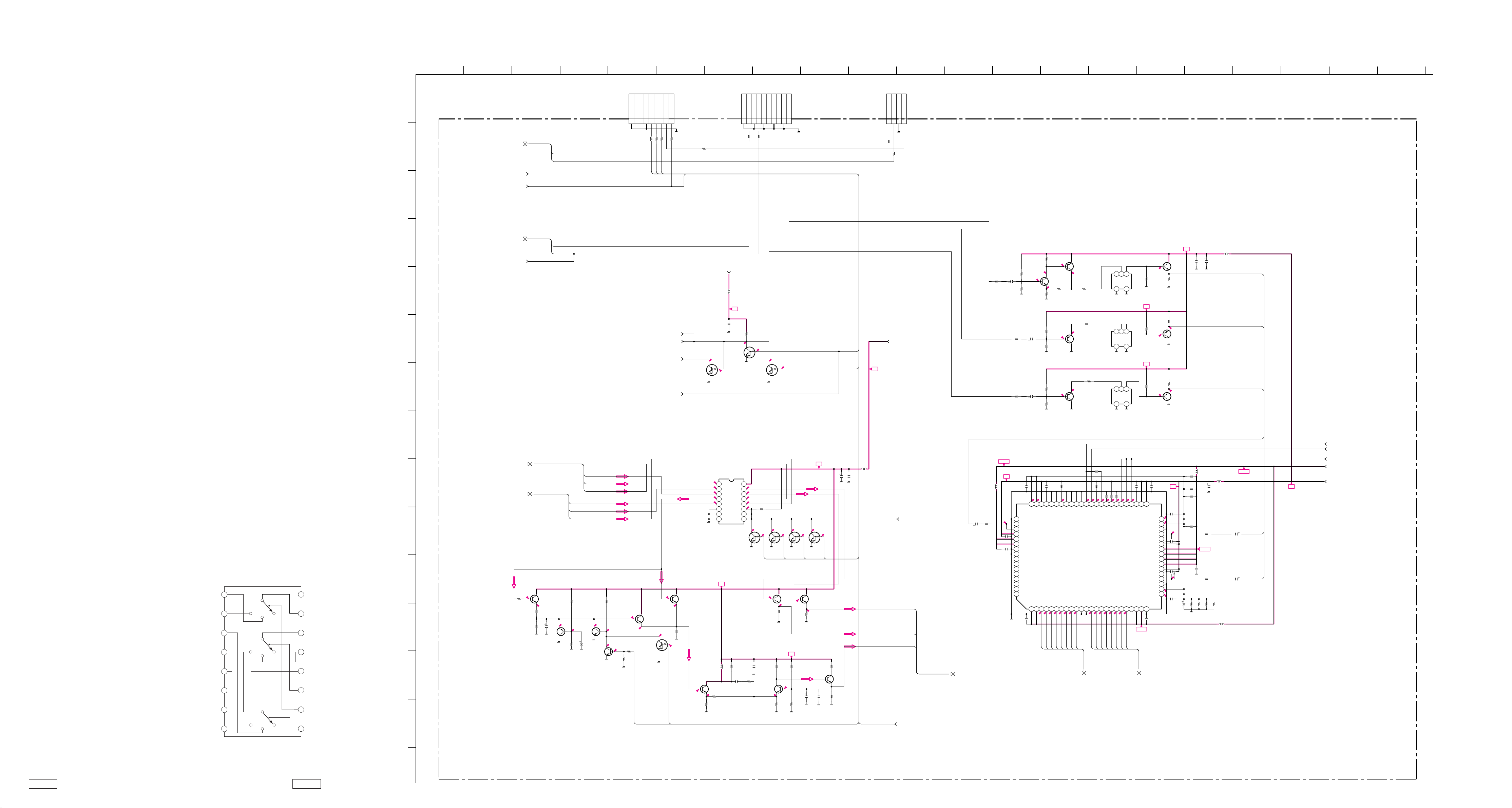
1
A
B
C
D
E
F
G
H
I
K
L
M
N
O
J
2
12
13
11
10
98765
43
14
2120191817
1615
5V
5V
5V
2.3
2.9 2.2
2.4
3.7
3.1
3.1
3.73.6
2.9
0
2.9 0.4
0
0.4
0.3
0.4
00
2.0
2.9
3.5
3.7
2.2
3.6
3.6
1.9
3.7
3.7
3.7
2.2
5.0
5.0 5.0 5.0 5.0
0.30.300
5V
5V
5V
5V
5V
4.3
1.0
0.9
1.5
4.3
2.3
1.7
2.3
1.7 3.22.6
3.2
2.6
1.6
1.6
2.3
1.7
1.5
1.5
1.2
1.2
3.3V
3.3V
5V
3.3V
5V
0.5
0.8
1.0
1.6
1.3
1.1
0.9
2.0
2.0
1.9
2.0
2.1
2.0
1.8
2.4
1.6
1.6
4.8
3.1
3.1
1.9
4.904.8
2.3
2.3
0
3.3V
5V
0.3
0.3
0.1
2.3
2.3
2.3
2.2
0.5
Y
Y
B-Y
R-Y
Y
Y
Y
Y
Y
B-Y
R-Y
Y
B-Y
R-Y
R-Y
B-Y
12345678
9 10 11 12 13 14 15 16
1 2 3 4 5 6 7 8 9 10 11 12 13 14 15 16 17 18 19 20 21 22 23 24
25
26
27
28
29
30
31
32
33
34
35
36
37
38
39
40
414243444546474849505152535455565758596061626364
65
66
67
68
69
70
71
72
73
74
75
76
77
78
79
80
123456789
1 2 3
46
1 2 3
46
1 2 3
46
123456789
10
123
4
R8740
R8741
R8742
R8743
R8744
R8745
R8746
R8747
R8748
R8750
R8751
R8752
R8754
R8756
R8757
R8758
R8759
R8760
R8761
R8762
R8763
R8764
R8765
R8766
R8767
R8768
R8769
R8770
R8771
R8772
R8773
R8774
R8775
R8777
R8778
R8779
R8780
R8781
R8782
R8784
R8785
R8789
R8790
R8791
R8792
R8793
R8794
C8657
C8658
C8659
C8660
C8661
C8662
C8663
C8664
C8666
C8667
C8668
C8669
C8670
C8672
C8673
C8674
C8675
C8676
C8678
C8679
C8680
C8681
C8683
C8684
C8686
C8687
L8535
L8536
L8541
FL8513
FL8514
FL8515
R8651
R8652
R8653
R8801
R8802
R8805
CN8505
CN8503
CN8504
R8811
L8542
R8812
R8813
R8814
C8692
R8816
R8818
C8693
C8694
R8819
C8671
C8691
R8815
R8817
R8821
L8543
R8822
R8823
R8825
R8824
Q8549
Q8533
IC8523
Q8527
Q8528
Q8529
Q8532
Q8530
L8539
L8540
IC8524
L8537
C8677
Q8539
Q8540
Q8541
Q8542
Q8545
Q8544
Q8543
Q8535
Q8537
Q8554
Q8531
Q8526
Q8552
Q8553
Q8534
Q8536 Q8538 Q8548
Q8550
L8538
R8783
R8786
47
16V
:AL-CP
1k
:CHIP
1k
:CHIP
33
:CHIP
33
:CHIP
68
:RN-CP
68
:RN-CP
68
:RN-CP
68
:RN-CP
47
16V
:AL-CP
68
:RN-CP
68
:RN-CP
33
:CHIP
47
16V
:AL-CP
10
:AL-CP
10
:AL-CP
47
16V
:AL-CP
47
16V
:AL-CP
10
:AL-CP
10
:AL-CP
10
16V
:AL-CP
10
16V
:AL-CP
10
16V
:AL-CP
0.1
25V
F:CHIP
0.1
25V
F:CHIP
0.1
25V
F:CHIP
0.1
25V
F:CHIP
0.1
25V
F:CHIP
0.1
25V
F:CHIP
0.1
25V
F:CHIP
0.1
25V
F:CHIP
0.1
25V
F:CHIP
0.1 25V F:CHIP
0.1
25V
F:CHIP
220
:CHIP
22k
:CHIP
470
:CHIP
22k
:CHIP
47k
:CHIP
47k
:CHIP
22k
:CHIP
100
:CHIP
100
:CHIP
100
:CHIP
470
:CHIP
47k
:CHIP
390
:CHIP
220
:CHIP
1.5k
:RN-CP
1k
:CHIP
1.5k
:RN-CP
1k
:CHIP
150
:RN-CP
150
:RN-CP
0.1
25V
F:CHIP
470
:CHIP
0.1
25V
F:CHIP
100k
:CHIP
10k
:CHIP
100k
:CHIP
22k
:CHIP
4.7k
:CHIP
470
:CHIP
10k
:CHIP
33k
:CHIP
47k
:CHIP
470
:CHIP
470
:CHIP
100
:CHIP
100
:CHIP
10k
:CHIP
0.1
25V
F:CHIP
1k
:CHIP
1k
:CHIP
1k
:CHIP
10k
:CHIP
0
:CHIP
0
:CHIP
Hm601
:CHIP
Hm601
:CHIP
Hm601
:CHIP
9P
BLK
:S-MICRO
0.1
25V
F:CHIP
27p
CH:CHIP
2.2
16V
F:CHIP
10
16V
:AL-CP
0.01
F:CHIP
10P
YEL
:S-MICRO
4P
BLK
:S-MICRO
4.7µH
:MLF2012
0
:CHIP
470
:CHIP
470
:CHIP
100
:CHIP
1k
:RN-CP
1.2k
:RN-CP
1k
:CHIP
22k
:CHIP
18k
:CHIP
1k
:CHIP
100
:CHIP
Hm601 :CHIP
0 :CHIP
0 :CHIP
0 :CHIP
#
DTC144EKA
INV
DTC144EKA
INV
MC74HC4053FEL
M/R-SW
2SB709A
CLAMP
2SD601A
SW
2SD601A
SW
DTC144EKA
SW
2SD601A
INV
0
:CHIP
0
:CHIP
CXD2303AQ
CHROMA DECODER
0
:CHIP
0.1
25V
F:CHIP
2SD601A
BUFF
2SB709A
BUFF
2SB709A
BUFF
2SB709A
BUFF
2SB709A
BUFF
2SB709A
BUFF
2SD601A
BUFF
2SD601A
BUFF
2SD601A
BUFF
2SD601A
BUFF
2SD601A
BUFF
2SD601A
BUFF
2SD601A
BUFF
2SD601A
BUFF
DTC144EKA
SW
DTC144EKASWDTC144EKASWDTC144EKA
SW
DTC144EKA
INV
0
:CHIP
68
:RN-CP
330
:RN-CP
A5V
D3.3V-2
A5V
RC-OUT
MID OUT
BUS
P-SYNC
B IN
A IN
2OUT
2YS
D5V
XOC
RC/MID≠≠≠≠≠
720P
OC
OC1
NORM1
CLP
ADCLK
OC
P-HD
480P
U
Y
V
V
U
Y
NORM
Z-WZ
480P
Z-WZ
NORM
NORM
480P
480P
2R-Y(RC)
2Y(RC)
2B-Y(RC)
2Y(MID)
2B-Y(MID)
2R-Y(MID)
SDA
VD
HD
SCL
BIN1
BIN2
BIN3
BIN4
BIN5
BIN6
BIN7
BIN8
AIN1
AIN2
AIN3
AIN4
AIN5
AIN6
AIN7
AIN8
2Y(SEL)
2B-Y(SEL)
2R-Y(SEL)
2YS
2YS
NORM
720P
720P
720P
AVSS
CIN
CIO
AVDD
CRT
CRTS
DVSS
DVSS
DVDD
DVDD
DVSS
DVSS
A7
AVSS
ARBS
ARB
AVSS
AIN
AIO
AVDD
ART
ARTS
BRTS
BRT
AVDD
BIO
BIN
AVSS
BRB
BRBS
AVDD
AVDD
TEST
XAOE
XBOE
XCOE
CTL0
CTL1
CTL2
SY
SEL
CLP
REF0
REF1
REF2
REF3
CLE
TEST
AVSS
AVSS
AVDD
CRBS
CRB
DVDD
DVDD
YGR
ADCLK
U-R
U-M
Y-R
YOUT
Y-M
INH
VEE
GND
VCC
UOUT
VOUT
V-R
V-M
USEL
USEL
YSEL
C0
C1
C2
C3
C4
C5
C6
C7
B0B1B2B3B4B5B6
B7
A0A1A2A3A4A5A6
E
E
480P
Z-WZ
NORM
E
E
E
VDEHD
P-RYEP-BY
P-Y
720P
E
MID-SCL
MID-SDA
OSD-SW
N.C
BR
(CHROMA DECODER,MID/RC SW)
(3/3)
TO(1/3)
TO(2/3)
TO(2/3)
TO(2/3)
TO(1/3)
TO(2/3)
TO(1/3)
TO(1/3)
TO(1/3)
TO(1/3)
TO A(1/4) BOARD CN003TO A(1/4) BOARD CN5501TO A(1/4) BOARD CN5701
N.C.
N.C.
TO(2/3)
FROM(1/3)
TO(2/3)
TO(2/3)
TO(2/3)
TO(2/3)
TO(1/3)
TO(1/3)
TO(1/3)
TO(2/3)
TO(2/3)
B-SS609.<U/C>-BR.-P3
BR (3/3) BOARD : IC8523 MC74HC4053FEL
B1
1
B0
2
3
C1
C. COM
INH
VEE
VSS
4
C0
5
6
7
8
OPEN
OPEN
OPEN
VDD
16
15
B. COM
A. COM
14
A1
13
A0
12
11
A
10
B
9
C
Schematic diagram
? BR (2/3) board
– 133 –
Schematic diagram
BR (3/3) board /
– 134 –
– 135 –
– 136 –
Page 91
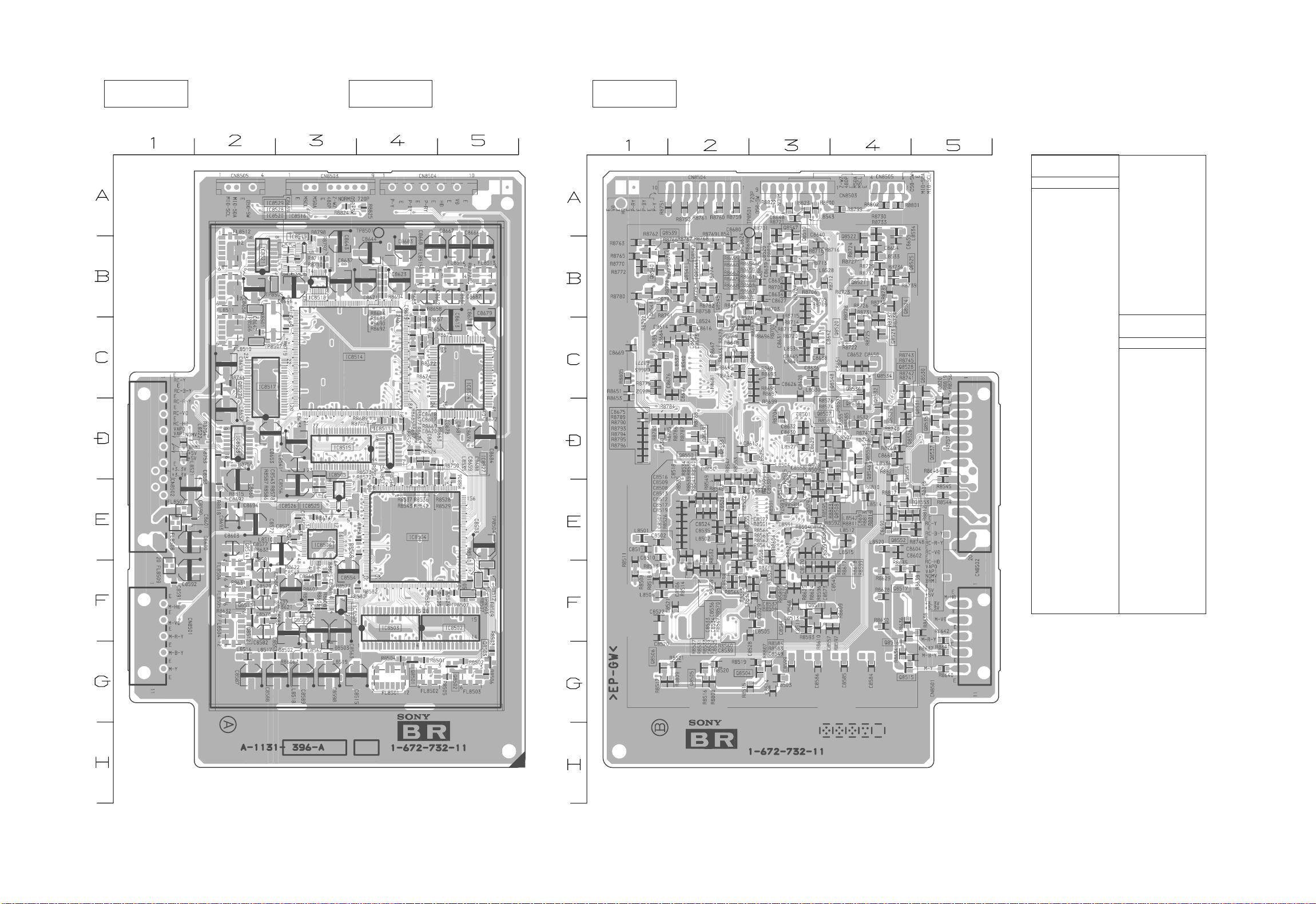
BR (1/3)
– BR Board –
TBC,FIELD MEMORY,
[ ]
3CH 8BIT A/D CONVERTER, PLL
BR (2/3)
[ ]
UP CONVERTER, 1MB MEMORY
BR (3/3)
[ ]
CHROMA DECODER, MID/RC SW
BR BOARD
TRANSISTOR
LR
Q8501 G-4 2
Q8502 G-5 2
Q8503 G-5 2
Q8504 G-3 1
Q8505 G-2 1
Q8506 G-1 1
Q8508 E-4 1
Q8509 F-3 2
Q8511 F-3 1
Q8512 F-2 2
Q8513 F-2 2
Q8514 F-2 2
Q8515 G-4 1
Q8516 F-4 1
Q8517 F-4 1
Q8519 B-3 1
Q8520 C-4 1
Q8521 B-4 1
Q8522 B-4 1
Q8523 C-4 1
Q8524 B-4 1
Q8525 B-4 1
Q8526 D-4 1
Q8527 C-2 1
Q8528 D-4 1
Q8529 D-4 1
Q8530 C-5 1
Q8531 D-5 1
Q8532 C-4 1
Q8533 D-2 1
Q8534 C-4 1
Q8535 D-5 1
Q8536 C-4 1
Q8537 D-5 1
Q8538 D-4 1
Q8539 B-1 1
Q8540 B-1 1
Q8541 B-2 1
Q8542 B-2 1
Q8543 B-1 1
*
Q8544 B-2 1
Q8545 B-2 1
Q8546 D-4 1
Q8547 B-3 1
Q8548 C-4 1
Q8549 D-2 1
Q8550 D-2 1
Q8551 D-4 1
Q8552 E-4 1
Q8553 E-4 1
Q8554 E-4 1
IC
LR
IC8502 F-5
IC8503 F-4
IC8504 E-4
IC8505 E-3
IC8506 E-3
IC8507 F-3
IC8511 D-4
IC8514 C-3
IC8515 D-3
IC8516 B-3
IC8517 C-2
IC8518 B-3
IC8519 B-3
IC8520 B-3
IC8521 B-2
IC8523 D-2
IC8524 C-5
IC8525 E-3
IC8526 E-3
IC8527 D-4
IC8528 B-3
IC8529 B-3
L ; component side
R ; conductor side
< Component Side >
– 137 –
< Conductor Side >
– 138 –
Page 92

G BOARD
DIODE *
D6001 G-8 D6002 H-7 D6003 G-9 D6004 I-4 D6005 F-9 D6006 F-9 D6007 H-6 D6009 H-5 D6010 J-4 D6011 F-8 D6012 F-8 D6013 J-7 D6014 J-4 D6015 E-7 D6016 H-3 D6017 H-3 D6018 H-3 D6019 H-3 D6020 I-3 D6021 H-2 D6022 H-3 D6023 I-1 D6024 I-2 D6025 H-2 D6026 H-1 D6027 H-1 D6028 H-2 D6029 H-1 D6030 H-2 D6031 I-2 D6032 H-5 D6033 I-2 D6034 J-3 D6035 J-3 D6101 C-5 D6102 D-8 D6103 D-6 D6104 D-6 D6105 E-8 D6106 D-7 D6107 D-7 D6108 C-9 D6109 D-5 D6110 A-4 -
D6111 B-9 D6112 B-9 D6113 E-8 D6114 D-1 D6116 C-1 D6117 D-9 D6119 D-10 D6120 E-10 D6121 B-4 D6122 B-4 D6123 A-9 D6124 A-9 -
D6125 B-9 -
TRANSISTOR *
Q6001 J-3 Q6002 J-4 Q6003 J-4 Q6004 I-4 Q6005 J-4 Q6006 J-4 Q6007 F-4 Q6008 G-3 Q6009 F-2 Q6010 G-2 Q6011 J-4 Q6012 J-3 Q6013 J-3 Q6101 B-4 Q6102 B-9 Q6103 B-9 Q6104 C-9 Q6106 C-10 -
IC
IC6001 F-8
IC6002 I-3
IC6003 J-2
IC6004 I-2
IC6005 E-1
IC6011 E-1
IC6101 C-4
IC6102 C-4
IC6103 C-4
IC6104 C-10
IC6301 D-2
G
[ ]
POWER SUPPLY
– G Board –
– 139 –
– 140 –
Page 93

A
B
TO GA BOARD
C
TO A(1/4) BOARD
D
E
F
G
H
I
J
K
1
CN6004
2P
AC(W)
AC(L)
CN6502
ANT E
CN6103
1P
:FASTON
CN507
1
2
1
2
R6001
2.2M
1/2W
C6013
10
R6008
220k
1/2W
MTZJ-12B
R6007
47k
D6003
ERC04-06SE
RECT
D6001
ERC04-06SE
RECT
L6001 L6002
2
C6001
0.47
250V
4
:AC
R6002
1M
1/2W
F6001
10A
125V
D6032
UF4005PKG23
PROT
R6017
1k
4.6
Q6004
2SC3311A
PROT
0
R6022
47k
D6023
1SS133
PROT
2SC3311A
D6004
R6011
47k
R6012
4.7
:RF
C6009
22
400V
1
C6002
0.22
250V
:AC
3
R6029
22k
SOFT START
R6028
R6016
Q6002
3.7
4.6
R6030
C6027
10
C6028
0.001
3.7
D6024
1SS133
R6033
1.8k
:RN
47k
SOFT START RESET
SW
00.7
R6015 R6020
47k 4.7k
D6006
P6KE200
PROT
D6005
UF4005
PROT
IC6001
TOP209 PWMSW
5678
D
143.3
NC
NC
S
1
2
3
4
C6003
0.0022
250V
:E
C6004
0.0022
250V
:E
FB6104
JW(5)
FB6105
JW(5)
IC6003
R6031
4.7k
IR3M02 (OSC)
12345678
E.AMP1+
E.AMP1-
47k
FEEDBACK
DTC
1.6
C
RT
GND
9.1k
14.3
:RN
C1
R6032
1k
Q6003
2SC3311A
12.6
C6015
0.01
250V
C
S
VD6001
TNR14V471K
E.AMP2+
E.AMP2-
REF OUT
DPC
VCC
C2
E2
E1
2SA1309A
SOFT START
12.4
D6010
1SS133
SW
R6004
470k
1/2W
D6011
MTZJ-9.1A
BIAS
R6021
22
5.8
C6014
1 2 3 4
43
RY6001
D6013
1SS133
RY PROT
R6005
47
:FPRD
5.1
14.3
R6034
1k
14.3
6.1
9 10 11 12 13 14 15 16
6.1
D6033
1SS133
R6023
470k
Q6005
R6042
47k
R6043
820k
1/2W
D6012
1SS133
FEED BACK
47
25V
C6007
0.0047
250V
F
~
+-
~
D6002
C6006
RBV-1506
0.0047
RECT
250V
F
R6010
2.2
10W
:RB
RY6002
D6031
11ES4
2.6
D6014
1SS133
SOFT START
12.6
C6016
2.2
D6015
D1NL20U
RECT
C6017
100
15MM 15MM
R6006
220k
1/2W
1000
250V
C6012
R6013
100
470k
IC6004
IR2112
DRIVE
891011121314
NC
VDD
14.4
HIN
6.1
SD
6.1
LIN
VSS
NC
2.8
Q6006
2SA1309A
SOFT START
D6035
MTZJ-12B PROT
T6003
SRT
2
1
4
3
JW6003JW6002
C6010C6008
1000
250V
D6007
1SS133
R6014
47k
D6009
MTZJ-33B
PROT
HO
VB
VS
NC
VCC
COM
1 2 3 4 5 6 7
L0
R6018
22k
13.5
Q6012
2SA1309A
C6037
10
9
8
7
D6120
D1NL20U
6
RECT
5
F6002
6.3A
125V
891011121314
NC
D6020
11ES4
PROT
VDD
14.7
HIN
6.1
SD
6.1
LIN
VSS
NC
IC6002
IR2112
DRIVE
C6030
330p
B
79.2
D6028
MTZJ-20C
87.4
PROTECT
C6032
0.1
:MPS
73.4
D6025 D6027
UF4005
PROTECT
14.4
C6029
C6031
330p
1
B
D6026
MTZJ-20C
6.1
PROTECT
15.1
C6036
0.1
:MPS
D6034
1SS133
PROT
Q6013
2SC3311A
IC6104
BA05T
5V REG
IO
2.6
15.2
13.0
G
R6039 R6041
10k 10k
13.5
0
R6040 R6019
10k
L6113
JW(5)
C6137
220
25V
H0
VB
VS
NC
VCC
COM
1 2 3 4 5 6 7
L0
FB6004
JW(5)
D6030
MTZJ-20C
PROTECT
UF4005
PROTECT
FB6003
JW(5)
D6029
MTZJ-20C
PROTECT
14.4
10k
12.4
IC6011
PC123FY2
VCC SW
12.3
4.9
R6116
10k
C6145
1000
6.3V
Q6102
2SA1309A
LATCH
R6117
470
79.3
C6019
87.3
330p B
73.3
D6016
UF4005
PROT
14.4
C6018
330p
B
6.1
D6021
MTZJ-20C
PROT
Q6010
R6036
IRFI644G
22
:FPRD
79.0
Q6009
IRFI644G
SW
R6035
22
:FPRD
Q6011
2SB734
VCC SW
14.4
Q6001
2SC3311A
12.4
4
3
R6112
1k
4.9
4.9
0
C6115 R6120
100
25V
D6019
MTZJ-20C
C6020
0.1
:MPS
C6021
1
SW
R6038
4.7k
73.4
6.1
R6037
4.7k
C6035
10
4.9
1
2
3.8
R6121
10k
D6111
1SS133
PROTECT
R6119
10k
0
10k
D6018
UF4005
PROT
D6017
MTZJ-20C
PROT
FB6001
JW(5)
146.3
S
C6034
680p
1kV
73.4
S
2.8
D6112
1SS133
PROTECT
4.9
R6025
FB6002
:FPRD
JW(5)
D6022
MTZJ-20C
R6024
22
:FPRD
C6033
680p
1kV
IC6005
PC123FY2
VCC OUT
4
3
1 2 3
VOUT
SENSE
R6126
1k
0.6
R6125
4.7k
Q6103
2SC3311A
LATCH
22
79.0
R6027
4.7k
6.0
R6026
4.7k
C6023
0.039
1kV
1
R6128
1k
11.0
2
9.8134.8
COLLECTOR
0
146.3
Q6008
IRFI644G
S
SW
73.3
73.3
Q6007
IRFI644G
SW
S
C6025
680p
1kV
T6001
PIT
1
2
3
4
6
R6115
220
:FPRD
GND
VCC CONTROLER
Q6104
2SC3311A
VCC SW
C6026
680p
1kV
15
12
13
10
14
11
18
15
16
13
17
14
8
18
7
16
9
17
12
8
10
7
11
9
IC6101
SE135N
98765
135V
R6113
10k
D6124
1SS133
PROT
C6150
0.1
:PT
C6022
0.015
800V
F6105
5A
F6106
5A
PS6102
5A
PS6101
5A
D6123
1SS133
PROTG
10
2
3
4
5
6
D6109
SF10SC3L
RECT
R6142
4.7k
0
0.2
R6104
470
:RN
R6103
4.7k
:RN
C6102
100
25V
T6002
PIT
8
10
11
12
9
L6104
6.8µH
:LHL08
C6105
100p
500V
C6104
100p
500V
D6103
D1NL40
RECT
1234
IC6102
µPC393C
OVP OCP
S2L40F RECT
D1NL40 RECT
11
PS6104
7A
D6116
D25SC6M
RECT
PS6103
7A
D25SC6MR
D6105
D4SBS4-F
C6107 C6112
RECT
100p 100p
C6106 C6111
100p 100p
D6102
D10SC6M
RECT
L6103
6.8µH :LHL08
D6108
D10SC6M
RECT
D6117
D10SC6MR
RECT
D6104
S2L40F
RECT
D6107
D6106
R6143
4.7k
4.9
0
2.4
5 6 7 8
2.2
CAUTION
Confirm that of d+Max. Voltage within the standard value when
replacing IC6101.
D6114
RECT
FB6102
1.1UH
FB6101
1.1UH
R6110
C6103
47
25V
C6108
1k
C6153
100p
C6152
100p
C6151
100p
C6154
100p
D6113
1SS133
RECT
D6119
MTZJ-12B
R6124
0.47
:FPRD
R6123
0.47
:FPRD
0.47
:FPRD
C6110
100p
C6109
100p
C6141
100p
C6142
100p
C6143
100p
C6144
100p
:LHL10
C6117 C6126
10000
10V
135V
C6114
220
160V
C6113
47
160V
-135V
+135V
11V
47
25V
IC6103
µPC1093J-1T
REF VOLTAGE
2.4
3
1
2
R6108
4.7k
R6109
4.7k
R6129
2.2k
REF
C6122
2200
25V
R6135
4.7k
R6136
4.7k
L6107
10µH
2.4
12
13
19V
C6121
3300
35V
C6120
3300
35V
C6129
3300
35V
C6128
3300
35V
-19V
R6141
47
:FPRD
C6119
2200
25V
C6118
2200
25V
14.4
13.8
Q6106
2SA1309A
REG
R6130
4.7k
L6108
10µH
:LHL08
C6131R6122
L6109
10µH
100
:LHL08
25V
C6132
100
25V
11V
+15V
11V
L6110
10µH
:LHL08
C6133
100
25V
21.5V
L6112
10µH
7V
100
25V
C6125
:LHL08
3300
35V
C6124
3300
35V
L6106
10µH
:LHL08
R6118
0.22
:RS
11ES4 PROT
TP.OVP
R6102
270k
:RN
R6101
4.7k
:RN
L6111
10µH
:LHL08
R6111
22k
2W
:RS
2W
:LHL08
D6101
-21.5V
C6123
220
160V
L6105
10µH
TP6101
C6135
100
C6134
100
D6110
MTZJ-33C
C6116
100
TP6102
TP.+B 135V
C6127
47
160V
11V
Q6101
2SA1309A
PROT
0
R6134
1k
G
(POWER SUPPLY)
R6105
1k
D6122
1SS133
PROT
D6125
1SS133
PROT
R6133
4.7k
C6140
100
25V
12.2
B-SS609.<U/C>-G..
14
19V11V
16.5V
-16.5V
R6106
1k
33V
1
OFF MUTE
2
3
4
E(AUDIO)
5
E(AUDIO)
6
E(AUDIO)
7
8
TO K BOARD
CN2101
1
+21.5V
2
3
+16.5V
4
-16.5V
5
6
-21.5V
TO D(1/2) BOARD
CN5003
1
2
3
4
5
6
7
8
9
TO A(1/4) BOARD
CN504
PROT
D6121
MTZJ-7.5B
R6132
1k
1
+135V
2
3
-135V
4
5
+16.5V
6
-16.5V
TO D(1/2) BOARD
CN5002
:S-MICRO
1
RM+5V
2
3
RELAY
4
5
+B OCP
6
+B OVP
7
TO A(1/4) BOARD
CN505
15
CN6102
8P
:VH
-19V
-19V
+19V
+19V
CN6105
6P
WHT
:S-MICRO
E
E
CN6104
9P
WHT
:S-MICRO
E
+15V
E
+7V
+7V
E
+11V
E
+33V
CN6106
6P
:MINI
E
E
CN6101
7P
BLK
E
PROT
NC
VDD
HIN
SO
LIN
VSS
Schematic diagram
? G board
G BOARD : IC6003 IR3M02
NON
INV
INV
REF
INPUT
INPUT
16 15 14 13 12 11 10 9
ERROR
AMP
2
ERROR
AMP 1
OUT
OUTPUT
CONTROL
REFERENCE
REGULATOR
0.1V
Vcc C
2
OSCILATOR
12345678
R
NON
INV
INPUT
INV
INPUT
FEED
BACK
DEAD
TIME
CONTROL
C
T
T
G BOARD : IC6002, 6004 IR2112
9
Q
R
10
S
VDD/Vcc
LEVEL
SHIFT
PULSE
11
VDD/Vcc
12
S
Q
R
LEVEL
SHIFT
13
G BOARD : IC6102 µPC393C
GND
4
5
IN2
IN1 IN
3
6
IN OUT2 V–
OUT1
1
2
8
7
E
GND
GEN
2
E
1
C
1
6
VB
UV
DETECT
PULSE
FILTER
PULSE
FILTER
DELAY
R Q
R
S
7
HO
VS
5
3
Vcc
1
LO
2
COM
Schematic diagram
K board /
– 141 –
– 142 –
– 143 –
Page 94

1
2
43
98765
10
11
12
13
14
1615
2120191817
22
A
B
C
D
E
F
G
H
I
J
K
L
M
CN2103
10P
WHT
:S-MICRO
L
E
R
E
SP SW
F MUTE
C MUTE
S MUTE
FIX MUTE
A MUTE
TO A(1/4) BOARD
CN512
CN2102
7P
WHT
:S-MICRO
CLK
DATA
ENABLE
E
MSCL
MSDA
A PROT
TO A(1/4) BOARD
CN510
CN2101
8P
WHT
:VH
OFF MUTE
-19V
-19V
E
E
E
+19V
+19V
TO G BOARD
CN6102
AUDIO L
1
2
3
4
5
6
7
8
9
10
Q2105
2SD601A
C MUTE BUFF
00
R2166
4.7k
:CHIP
D2101
MA111
C2166
22
1
2
3
4
5
6
7
1
2
3
4
5
6
7
8
R2133
100
:CHIP
8.8
4.0
Q2101 Q2102
2SD601A
FIXED L
3.4
R2137
R2134
1k
100
:CHIP
:CHIP
AUDIO R
D2111D2112
MA111MA111
MA111 MA111 MA111 MA111 MA111
12V
D2102
R2139
22k
:CHIP
R2140
:CHIP
11.9
22k
MA111
Q2103
2SB709A
ON POP
0
R2141
4.7k
:CHIP
C2160 C2162
3300
35V
C2161 C2163
3300 35V
0.1
:PT
0.1
:PT
R2136
:CHIP
4.0
3.4
R2135
100
:CHIP
10 25V :BP
D2110
MA111
D2116
MA111
-0.9
Q2104
2SB709A
OFF POP
R2143
100
:CHIP
C2167
470
16V
-19V
19V
100
8.8
C2165
R2104
R2105
R2107
R2106
:CHIP
FIXED L
2SD601A
FIXED R
FIXED R
R2138
1k
:CHIP
C2164
10 25V :BP
F MUTE
C MUTE
S MUTE
FIX MUTE
D2107D2106D2105D2104D2103
VAR MUTE
+12 V
D2108
MA111
11.4
11.3
D2109
MA111
A PROT
270
3W
150
3W
150
3W
0
SP/SW
R2142
10k
:CHIP
+9V
9V
12V
R2124
15k
:CHIP
R2125
22k
:CHIP
R2144
15k
:CHIP
R2126
22k
:CHIP
R2164
8.2k
:CHIP
R2165
8.2k
:CHIP
R2167
330k
:CHIP
C2174
100
C2103 C2111
47
0.0022
25V
B:CHIP
14.1
C2113
C2105
0.0022
47
25V
B:CHIP
14.5
C2115C2107 C2116
0.0022
47
B:CHIP
25V
19.2
IC2102
MC7805CT
5V REG
IO
G
IC2103
PQ09RF21
9V REG
IO
G
IC2104
MC7812CT
12V REG
IO
G
C2157
R2129
:CHIP
12.0
R2145
47k
:CHIP
C2170
0.1
:PT
22
220k
12V
R2111
100
:CHIP
5.0
9.1
C2153
0.1 :PT
C2169
0.00068
15k
:CHIP
R2147
2.2M
:CHIP
C2104
47
25V
C2106
47
25V
C2108
47
25V
12V
+12 V
IC2301
NJM4558D
VAR. OUT AMP
6.0
1234
ROUT
VCC
R-IN
R+IN
VSS
C2149
0.1
:PT
:PT
C2147 C2144 C2140
0.047
:PT
4.2
4.3
1.2
RLC2
RLC1
CT
ST
COUT
4.1
4.1
4.1
6.0
LOUT
6.0
L-IN
6.0
5 6 7 8
L+IN
C2302
C2146
0.1
:PT
C2141C2145
C2143
0.22
0.22
4.7
:PT
:PT
C2139
0.68
:PT
0.22
C2142
:PT
4.7
4.1
4.4
4.4
4.3
PSC2
PSC5
PSC1
PSC4
RLC5
IC2105
NJW1103
PROLOGIC DECODER
SOUT
CMC
SMRO
SMRI
AGND
4.1
4.1
4.1
R2109
10k
:CHIP
C2118
C2173
0.1
:PT
47
25V
R2110
22k
:CHIP
D2113
UDZ-TE-17-10B
R2305
12k
:CHIP
C2329
25V
R2306
10k
:CHIP
0.22
:PT 0.047
4.1
4.1
4.3
PSC3
PSC6
DVDD
MIC IN
C2177
0.0022
B:CHIP
47
C2326
R2118 R2117
4.7k
:CHIP
C2135
0.00047
:PT
R2119
22k :CHIP
R2121
330k
:CHIP
R2120
:CHIP
C2136
C2138
680p
:PT
:PT
C2137
0.0056
4.1
4.1
0.2
4.1
LPIN
DBC1
DBC2
DBC3
DATA
SCK
REQ
TEST CNT
4.8
4.8
UDZ-TE-17-10B
R2307
47k
:CHIP
C2325
10
R2308
47k
:CHIP
10
R2115
47k
47k
:CHIP
:CHIP
22k
C2131
0.1
:PT
:PT
4.1
4.1
4.1
DBIN
S'OUT
FBIN EC
FBIN SU
DELAYSIG OUT
L01
L02
L03
XIN
XOUT
2.4
2.6
4.7
D2115
UDZ-TE-17-10B
D2114
R2116
4.7k
:CHIP
C2134
0.0015
:PT
C2132
0.1
:PT
4.1
2.5
414243444546474849505152535455565758596061626364
VOLOUT
LPF2OUT
DELAYSIG IN
LPF2IN2
LPF2IN1
DA INT OUT
DA INT IN
DA CONT
AD CONT
AD INT OUT
AD INT IN
LPF1 OUT
LPF1 IN2
LPF1 IN1
DELAY IN
MIX OUT
VREFD
AVDD
DVSS
AVSS
R2114
1M
:CHIP
X2101
4MHz
2.5
40
2.5
39
2.5
38
2.5
37
2.5
36
0
35
0.1
34
1.8
33
2.5
32
2.5
31
2.5
30
2.5
29
2.5
28
4.1
27
2.5
26
25
C2155
0.1 :PT
:PT
R2128
100k
:CHIP
C2158
10
C2176
0.0022
B:CHIP
C2168
100
R2113
100
:CHIP
R2148R2146
15k
:CHIP
R2127
2.2M
:CHIP
R2112
:CHIP
R2301
47k
:CHIP
R2302
47k
:CHIP
R2149
15k :CHIP
R2123
15k :CHIP
C2156
0.1 :PT
L
R
9V
100
C2154
0.00068
R2122
47k
:CHIP
4.1
4.1
4.1
4.1
4.1
C2171
0.1 :PT
4.1
4.1
4.1
4.1
4.1
1.3
2.6
:PT
4.0
4.2
65
66
67
68
69
70
71
72
73
74
75
76
77
78
79
80
4.2
C2159
0.0056
:PT
R2303
12k
:CHIP
6.0
6.0
R2304
10k
:CHIP
C2301
11
9V
C2150
0.1
:PT
C2148
0.047
C2151
0.022
:PT
C2152
0.022
4.1
4.1
:PT
RLC6
LLI
LBPF
RLI
RBPF
LT
RT
LIN
RIN
HOLDC
AVCC
VREFA
VREFG
IREF
NGC3
NGC2
C2117
47
25V
4.2
RLC4
RLC7
RLC3
RLC8
NGC1
LOUT
ROUT
12345678910 11 12 13 14 15 16 17 18 19 20 21 22 23 24
4.1
4.1
4.1
L
R
R
L
C2112
0.0022
5V
B:CHIP
C2114
0.0022
9V
B:CHIP
0.0022
12V 12V
B:CHIP
+5 V
+9 V
C2133
0.1
:PT
C2130
0.0018
:PT
C2128
0.068
:PT 0.1
C2125 C2126
0.068
:PT
C2124
0.0015
:PT
C2122
1
:PT
C2172
47
25V
5V
C2123
0.01
C2178
0.0022
B:CHIP
+12 V
C2129
0.01
:PT
:PT
C2127
:PT
0.1
:PT
C2121
22
R
9V
9V
+9 V
R
9V
L
C2303
22
C2327
47
25V
C2304
0.0027
SL:CHIP
4.5
C2305
4.5
0.0027
SL:CHIP
4.5
C2306
2.2
4.5
4.5
C2324
10 25V :BP
C2312
22
+9 V
C2328
47
25V
C2313
0.0027 SL:CHIP
4.5
C2314
4.5
0.0027
SL:CHIP
4.5
C2315
2.2
4.5
4.5
C2322
10 25V :BP
VAR L
VAR R
IC2302
TDA7312
L,R TONE CONT.
4.6
123456789101112131415
CREF
VS
GND-DIGDIG OUT1
GND
TRE-L
TRE-R
IN(R)
DIG OUT2
BOUT(R)
OUT(R)
BOUT(L)
R4
R3
R2
R1
L4
L3
IC2303
TDA7312
C,S TONE CONT.
123456789101112131415
CREF
VS
GND-DIGDIG OUT1
GND
TRE-C
TRE-S
IN(S)
DIG OUT2
OUT(S)
BOUT(S)
S4
BOUT(C)
S3
S2
S1
C4
C3 C2
SCL
SDA
L OUT
R OUT
ADDR2
ADDR1
BIN(R)
BIN(L)
OUT(L)
IN(L)
L1
L2
SCL
SDA
C OUT
S OUT
ADDR2
ADDR1
BIN(S)
BIN(C)
OUT(C)
IN(C)
C1
D2301
3.7
UDZ-10B
3.6
4.6
UDZ-10B
4.6
4.5
0.1 25V F:CHIP
4.5
4.5
0.1 25V F:CHIP
4.5
4.5
C2311
4.5
4.5
C2323
10 25V :BP
16 17 18 19 20 21 22 23 24 25 26 27 28 29 30
D2303
3.74.5
UDZ-10B
3.6
4.6
UDZ-10B
4.6
4.5
0.1 25V F:CHIP
4.5
4.5
0.1 25V F:CHIP
4.5
4.5
4.5
4.5
16 17 18 19 20 21 22 23 24 25 26 27 28 29 30
D2302
C2307
C2308
F:CHIP
C2309
C2310
0.1
25V
F:CHIP
2.2
D2304
C2316
C2317
0.1
25V
F:CHIP
C2318
C2319
0.1
25V
F:CHIP
C2320
C2321
10
25V
:BP
R
0.1
25V
2.2
L
L
R2313
100
:CHIP
R2314
100
:CHIP
R2309
5.6k
:CHIP
R2310
5.6k
:CHIP
R2315
100
:CHIP
R2316
100 :CHIP
R2311
5.6k
:CHIP
R2312
5.6k
:CHIP
9V
SP/SW
S MUTE
C MUTE
F MUTE
19V
19V
R
A PROT
FIX MUTE
VAR MUTE
L
R2632
10k
:CHIP
2SD601A
L/R MUTE 1
C2612
C2601
-19V
FIXED L
FIXED R
C2804
10
R2633
100k
:CHIP
0.2
Q2606
19V
-19V
9V
9V
1
R2614
:CHIP
-19V
12V
1
C2801
1
C2802
1
:CHIP
R2813
470k
:CHIP
+9V
C2623
10
C2624
10
11.6
10k
IC2603
TDA7265
S AMP
R2601
22
:CHIP
R2602
22
:CHIP
R2607
10k
:CHIP
Q2601
2SD601A
S MUTE 1
470
R2618
39k
:CHIP
0.2
R2802
470
:CHIP
R2801R2805
0.5
IN-(R)
R2640
:CHIP
C2625
47
25V
1
R2617
39k
:CHIP
R2620
5.6k
:CHIP
-19 V
+19 V
IN-(SR)
R2605
33k
:CHIP
C2602
10
10k
:CHIP
D2601
MA111
:CHIP
R2810R2814
470k
:CHIP
470
10.2
10.8
10.2
R2621
:CHIP
GND
C2605
10
-19V
470k
:CHIP
GND
22
R2659
:CHIP
C2608
1
470
:CHIP
R2804
470k
:CHIP
C2803 R2811
10 470
IN+(R)
00000
R2637
470
RL
:CHIP
R2638 R2639
470
18k
:CHIP
:CHIP
R2634
10k
:CHIP
D2613
C2621
1
MA111
C2614
R2616
10k
:CHIP
Q2603
2SB709A
C MUTE
R2619
4.7k
:CHIP
IN+(SR)
0000
R2604
390
:CHIP
R2608 R2609
100k
11.5
:CHIP
+19V
0.2
VAR MUTE BUFFER
R2819
10k
:CHIP
Q2806
2SD601A
FIX MUTE BUFFER
R2820
10k
:CHIP
IC2601
TDA7265
L,R AMP
IN-(L)
IN+(L)
-VS(L)
R2642
18k :CHIP
R2641
R2643
470
18k
:CHIP
:CHIP
R2644
18k
:CHIP
C2626
47
25V
C2613
1
IN-(SL)
33k
R2606
390
:CHIP
10.7
R2610
:CHIP
R2636
33k
:CHIP
Q2607
2SD601A
L/R MUTE 2
R2635
15k
:CHIP
+19 V
IN+(C)
IN-(C)
R2624
000
33k
:CHIP
R2622
22k
:CHIP
R2625
R2623
:CHIP
C2615
IN+(SL)
0 10.1 0 0
15k
390
10
-VS(SL)
MUTE
10k :CHIP
10.1
R2611
33k
:CHIP
10.1
Q2602
2SD601A
S MUTE 2
22k
:CHIP
0.1 :PT
VAR L
VAR R
Q2805
2SD601A
FIXED L
FIXED R
MUTE
OUT(L)
10.2
R2647
27k
:CHIP
C2622
0.1
:PT
R2662
10k
:CHIP
-19 V
+9 V
IC2602
TDA2052
C AMP
IN+(MUTE)
-VS
C2617
0.1
:PT
OUT(SL)
R2660
C2606
UDZ-TE-17-10B UDZ-TE-17-10B
UDZ-TE-17-10B UDZ-TE-17-10B
R2809
4.7k
0
:CHIP
R2808
47k
:CHIP
R2817
:CHIP
+VS
00
R2648
27k
:CHIP
MUTE
-15.4
+VS
OUT(SR)
C2607
0.1
:PT
C2609
0.1
:PT
0
4.7k
0
OUT(R)
+VS
1234567891011
2SD601A
FIX MUTE 2
R2818
47k
:CHIP
-VS(R)
1234567891011
C2632
L
OUT(C)
1234567
0
C2618
0.1
:PT
C2620
4.7
D2611
MA111 MA111
R2656
27k
:CHIP
-VS(SR)
C2610
0.1
:PT
D2621 D2622
D2623 D2624
0
Q2802
2SD601A
VAR MUTE 2
R2815
4.7k
0
:CHIP
R2816
Q2804
:CHIP
R
R2645
100
4.7
25V
1W
:RS
C2627
0.1
:PT
R2650
47k
:CHIP
D2618
MA111
0
R2649
12k
:CHIP
R2658
27k
:CHIP
D2609
MA3220M-TX
R2626
4.7
1W
:RS
C2619
0.1
:PT
D2610
MA3220M-TX
R2629
:CHIP
R2628
47k
:CHIP
2SD601A
C SP/SW 2
R2627
47k
:CHIP
+12V
R2657
27k
:CHIP
R2612
4.7
1W
:RS
R2806
4.7k
:CHIP
0
FIX MUTE 1
47k
R2646
C2628
D2615
MA3220M-TX
9.1
Q2608
2SD601A
PROT 1
R2652
100
:CHIP
C2633
39k
0.1
0
Q2604
R2613
4.7
1W
:RS
C2611
0.1
:PT
0
R2807
VAR MUTE 1
47k
:CHIP
MA3091-TX
MA3091-TX
Q2803
2SD601A
D2614
MA3220M-TX
4.7
1W
:RS
0.1
:PT
R2651
R2653
1k
1k
:CHIP
:CHIP
9.1
0
Q2609
2SD601A
PROT 2
0
100
50V
:BP
12.0
R2630
1k
:CHIP
0.1
R2631
10k
:CHIP
D2801
MA3091-TX
D2802
MA3091-TX
D2803
MA3091-TX
0
Q2801
2SD601A
D2804
MA3091-TX
D2805
D2806
MA3091-TX
D2807
MA3091-TX
D2808
D2616
MA3220M-TX
D2617
MA3220M-TX
Q2610
2SB709A
PROT 3
9.1
0
R2663
10k
:CHIP
R2655
:CHIP
R2654
10k
:CHIP
D2605
MA3220M-TX
D2606
MA3220M-TX
RY2601
D2612
2SD601A
C SP/SW 1
D2602
MA3220M-TX
D2603
MA3220M-TX
1k
C2631
100 25V
Q2605
L
R
L
R
D2607
MA3220M-TX
D2608
MA3220M-TX
D2604
MA3220M-TX
D2620
MA3220M-TX
J2601
L VAR/FIX
AUDIO OUT
J2602
R VAR/FIX
AUDIO OUT
CN2601
4P
WHT
:S-MICRO
1
TW L
2
L.E.
3
TW R
4
R.E.
CN2602
4P
WHT
:MINI(LOCK)
1
SP(L)
2
L.E.
3
SP(R)
4
R.E.
TB2601
-
CENTER
+
SPEAKER IN
CN2603
2P
WHT
:MINI(LOCK)
1
SP(C)+
2
SP(C)-
TB2602
REAR L
SP OUT
+
REAR R
+
SP OUT
VAR L
FIXED L
VAR R
FIXED R
TWEETER
(L)
TWEETER
(R)
SPEAKER
(L)
SPEAKER
(R)
CENTER
SPEAKER
N
O
– 144 –
+19 V
-19 V
19V
-19V
(AUDIO AMP,AP,DOLBY,I/O)
K
B-SS609.<U/C>-K..
– 146 –– 145 –
Page 95

AUDIO AMP, TONE CONTROL,
[ ]
K
PROLOGIC DECODER
– K Board –
K BOARD
DIODE
LR
D2101 J-7 3
D2102 I-6 3
D2103 I-5 3
D2104 I-5 3
D2105 I-5 3
D2106 I-5 3
D2107 I-6 3
D2108 I-7 3
D2109 I-7 3
D2110 J-6 3
D2111 J-5 3
D2112 J-5 3
D2113 F-7 3
D2114 F-8 3
D2115 F-8 3
D2116 I-6 3
D2301 E-6 3
D2302 E-7 3
D2303 D-6 3
D2304 D-6 3
D2601 A-1 3
D2602 B-3 4
D2603 B-3 4
D2604 B-4 4
D2605 B-5 4
D2606 B-5 4
D2607 B-5 4
D2608 B-5 4
D2609 H-2 4
D2610 H-1 4
D2611 I-2 3
D2612 I-1 3
D2613 E-4 3
D2614 I-2 4
D2615 I-9 4
D2616 I-3 4
D2617 I-3 4
D2618 G-3 3
D2620 B-4 4
D2621 A-3 3
D2622 A-4 3
D2623 A-3 3
D2624 A-3 3
D2801 A-7 4
D2802 A-6 4
D2803 B-7 4
*
D2804 B-6 4
D2805 A-7 4
D2806 A-6 4
D2807 A-8 4
D2808 A-8 4
TRANSISTOR
LR
Q2101 D-5 1
Q2102 D-5 1
Q2103 I-6 1
Q2104 J-7 1
Q2105 J-6 1
Q2601 B-1 1
Q2602 B-2 1
Q2603 G-5 1
Q2604 I-1 1
Q2605 I-1 1
Q2606 E-4 1
Q2607 E-3 1
Q2608 G-3 1
Q2609 G-2 1
Q2610 G-2 1
Q2801 A-7 1
Q2802 A-7 1
Q2803 A-6 1
Q2804 A-6 1
Q2805 C-5 1
Q2806 B-6 1
IC
LR
IC2102 H-2 H-8
IC2103 H-4 H-6
IC2104 H-3 H-8
IC2105 G-2
IC2301 B-2
IC2302 E-2
IC2303 C-2
IC2601 F-7 F-3
IC2602 F-5 F-4
IC2603 B-3
L ; component side
R ; conductor side
K BOARD : IC2301 NJM4558D
1
2
3
*
4
K BOARD : IC2601, 2603 TDA7265
L + IN
GND
R + IN
5
7
9
11
1
R-VS
MUTE / ST-BY
8
7
6
5
+VS
L-VS
K BOARD : IC2602 TDA2052
2
6
5
7
MUTE/
ST-BY
3
3
4
L OUT
L -IN
8
10
R -IN
2
R OUT
6
1
4
< Component Side >
– 147 –
< Conductor Side >
– 148 – – 149 –
Page 96

D BOARD
DIODE *
D5001 F-1 D5002 E-1 D5004 F-2 D5005 F-4 D5006 E-2 D5008 E-3 D5009 B-3 D5010 F-3 D5011 G-4 D5013 B-7 D5014 E-3 D5015 B-9 D5016 G-4 D5017 G-4 D5019 D-8 D5020 D-7 D5021 D-4 D5022 B-1 D5024 H-4 D5025 C-2 D5027 D-4 D5028 B-2 D8001 G-16 D8002 F-15 8
D8003 B-16 D8004 G-10 8
D8005 G-16 8
D8006 E-11 4
D8007 A-14 D8008 D-16 4
D8009 D-16 4
D8010 E-15 D8011 A-14 D8013 E-13 D8014 E-13 D8015 I-15 8
D8017 I-16 8
D8018 G-8 D8021 G-14 8
D8023 J-14 8
D8024 H-14 8
D8025 G-14 8
D8026 F-14 8
D8027 G-14 8
D8029 I-15 8
D8031 H-13 4
D8032 E-11 D8033 I-15 8
D8034 J-15 4
D8035 I-15 4
D8036 G-13 8
D8037 J-14 8
D8038 H-15 4
D8039 I-16 4
D8040 G-13 8
D8041 G-9 4
D8042 I-16 D8043 H-13 4
D8044 B-16 D8045 I-13 4
D8046 I-13 4
D8047 I-12 4
D8048 F-11 4
D8050 F-10 8
D8051 H-10 8
D8052 H-8 8
D8054 H-11 8
TRANSISTOR *
Q5002 A-3 Q5004 G-4 Q5005 F-2 Q5006 E-2 Q5008 B-3 Q5009 E-2 Q5010 F-2 Q5013 A-4 Q5014 E-4 Q5015 E-3 Q5016 E-4 Q5019 E-4 Q5022 G-7 Q5023 H-7 Q5024 G-6 Q5025 H-6 Q5026 H-8 Q5027 J-3 Q5029 D-2 Q5030 D-2 Q5031 D-5 Q5033 H-4 Q5034 B-2 Q5035 A-2 Q8001 G-16 -
Q8002 G-16 Q8003 F-16 Q8004 G-10 Q8005 G-16 Q8006 G-10 1
Q8007 B-15 Q8008 D-15 Q8009 H-15 1
Q8010 I-15 1
Q8013 G-10 1
Q8014 D-10 Q8015 H-16 Q8016 H-16 Q8017 G-9 Q8018 J-14 1
Q8019 G-15 1
Q8020 G-9 1
Q8021 G-15 1
Q8022 J-13 1
Q8023 G-15 1
Q8024 I-16 1
Q8025 I-16 1
Q8026 J-16 1
Q8027 G-12 1
Q8028 G-12 1
Q8030 H-13 1
Q8031 F-11 1
IC
IC5001 G-6
IC5002 G-7
IC5004 G-3
IC5005 I-4
IC5006 I-9
IC5008 C-2
IC5009 A-2
IC5010 C-3
IC8001 H-11
IC8002 I-15
IC8003 H-8
IC8004 E-9
IC8005 H-10
IC8006 H-13
IC8007 J-15
IC8008 J-13
IC8009 I-13
IC8010 H-14
IC8011 H-12
D (1/2)
– D Board –
[ ]
H DEFL, V DEFL, SUB DEFL
D (2/2)
[ ]
H DEFL, V DEFL, SUB DEFL
NOTE :
The circuit indicated as left contains high voltage of over
600 Vp-p. Care must be paid to prevent an electric shock in
inspection or repairing.
– 151 –– 150 –
– 152 –
Page 97

1
2
43
98765
10
11
12
13
14
1615
1817
A
B
C
D
E
F
G
H
I
J
K
L
TO G BOARD
CN6105
TO G BOARD
CN6106
TO ZG BOARD
CN4207
CN5003
6P
WHT
:S-MICRO
+21.5V
E
+16.5V
-16.5V
E
-21.5V
TO CHASSIS GND
CN5002
6P
WHT
:MINI
+135V
E
-135V
E
+16.5V
-16.5V
CN5001
3P
YEL
:S-MICRO
+135V
NC
E
1
2
3
4
5
6
1
2
3
4
5
6
1
2
3
-0.4
R5204
R5205
4.7k
R5200
10k
C5201
0.01
F
10k
TO (2/2)
+135V
R5203
4.7k
1234
8.3
7.0
C5200
47
16V
-12V
-21.5V
21.5V
135V
-135V
16.5V
-16.5V
IC5010
LM358P
3.8
5 6 7 8
Q5036
2SA1309A
H.DRIVE DET
5.7
R5214
10k
C5118
47
16V
R5199
22k
1.7
-12V
2.1
R5206
4.7k
-12V
C5116
47
C5122
0.01
F
R5216
2.7k
C5111
47
16V
12V
R5195
15k
1234
C5119
1000p
500V
B
+12V
R5194
1.5k
C5113
0.1
:PT
C5203
470p
:PT
6.2
R5215
47k
R5196
10k
IC5009
LM358P
H.SAW
6
C5107
0.1
:PT
R5217
10k
D5028
1SS133
2SA1309A
H.DRIVE PROT
R5179
4.7k
R5182
470k
C5120
0.01
F
C5108
220p
:PP
R5188
2SC2878AB
10k
0.5
R5190
0.47
:FPRD
R5192
2.2k
R5193
68k
0.3
0.3
C5112
0.3
5 6 7 8
11.8
Q5037
R5180
2.2k
R5181
2.7k
0
1234
0
0
0.5
Q5034
CLAMP2
0
Q5035
2SC3311A
H-SAW
12V
47
16V
12V
12V
D5025
1SS133
AND1
1.4
7.0
R5218
1k
IC5008
LM393P
PWM
R5187
15k
R5189
1k
R5191
R5197
100
C5114
0.001
:PP
C5121
0.01
F
C5204 C5205
0.0022
:PT
1.5
0.2
0
5 6 7 8
1k
0.0022
:PT
-12V
C5123
47
16V
C5124
0.01
F
R5183
2.7k
C5208
1000p
:PP
R5184
1k
D5022
1SS133
E-W
R5201R5186
JW(5)4.7k
123456789
EEPIN(E-W)EH.DRIVE
E
TO A(1/4) BOARD
CN509
12V
16.5V
E
V.BLK
TO CHASSIS
-16.5V
-135V
+16.5V
H.DRIVE
+12V
H.DRIVE
TO (2/2)
10
CN5004
:B TO B-P
H.BLK(HP)
E
GND
CN8002
:FASTON
GND
L5001
47µH
:LHL08
-12V
-16.5V
10P
-14.7 -12.0
IO
G
C5001
C5085
47
0.0022
25V
F
R5001
JW(7.5)
L5002
47µH
:LHL08
C5003
47
25V
-12V
R5003
1k
5.6
5.7
R5002
1k
2SA1309A
H.D.BUFF
C5097
100
16V
Q5029
2SC3311A
PIN DRIVE
3.8
Q5030
2SA1309A
PIN DRIVE
-11.5
C5098
100
16V
-135V
12V
R5004
4.7k
PROT
C5002
1
-12V
Q5004
2SC3311A
V.BLK BUFFER
0
-16.5V
16.5V
12V
C5090 R5155
1 4.7k
TO (2/2)
IC5001
NJM7912FA
-12V.REG
C5008
C5006
0.0022
14.5 12.2
C5004
0.0022
F
C5005
0.1
:PT
Q5002
R5165
47
1/2W
:FPRD
D5002
1SS133
D5004
1SS133
CLAMP
D5001
1SS133
PROT.5V
47
F
IC5002
NJM7812FA
+12V.REG
IO
G
C5014
0.0022
F
R5235
6.8k
3W
:RS
C5012
22
160V
C5016
0.047
Q5008
2SC2688
H.DRIVE 2.7k
-2.9
R5011 C5010
3.3k 100p
CH
R5166
220k
11.5
C5099
0.1
200V
3.6
:PT
R5167 R5169
47
1/2W
:FPRD
R5168
47
1/2W
:FPRD
D5006
1SS133
CLAMP
R5013
4.7k
C5011
47
0.1
Q5006
2SC3311A
H-DEF-PROT
-0.6
R5009
2.2k
MTZJ-T-77-5.6
C5007
100p
R5017
22k
R5012
4.7k
0.1
Q5005
2SC3311A
V-DEF-PROT
R+5V
-12V
C5017
47
R5026 R5032
6.8k
6.8k
3W
3W
:RS
:RS
2
200V
:PT
95.9
1
Q5031
2SK2251
PIN OUT
-125.0
10k
D5027
MTZJ-T-77-15
12.1
R5023
22k
R5018
3.3k
0.7
47k
H.P.
C5015
47p
R5022
22k
R5029
0.47
D5005
:FPRD
R5028
0.47
:FPRD
12.1
R5020
47k
1.7
C5013
47
R5021
11k
:RN
R5016
10k
0.6
R5034
10k
-12V
+12V
12V
6
7
R5031
1W
:RS
C5019
220p
500V
B
D5021
ERC91-02
-93.1
FB5001
0.45UH
S
-134.6
Q5009
2SA1309A
PROT.DELAY
0.8
R5033
1SS133
PEAK.DET1k
R5039C5020R5030
10k0.1
:PT
L5004
47µH
:LHL08
C5025
1000
25V
L5003
47µH
:LHL08
Q5010
2SA1309A
PROT.DELAY
R5038
JW(5)
R5035
10k
C5023
1
TO ZB BOARD
CN4304
H.OUT (B)NCNC
H.RET (B)
123
R5209
12
3W
:RS
TO (2/2)
TO (2/2)
TO (2/2)
T5001
HDT
45
3
2
1
L5018
5mH
R5175
10
3W
:RS
C5026D5008
0.01
:PT
Q5014
2SA1309A
BUFF
IC5004
STV9379
V.OUT
D5016
MTZJ-T-77-24A
:PROT
C5024
1000
25V
R5043
1k
C5028
470p
500V
R5040
1k
4
R-5V
L5016
15mH
L5017
15mH
C5096
D5009
330p
RGP15G
2kV
SPEED UP
-89.5
R5046
1.5
3W
-89.1
:RS
2SC3997S
3
R5049
10
3W
:RS
R5207
R5208
3.3
3.3
3W
3W
:RS
:RS
R5176
3W
:RS
R5050
100
12.2
Q5015
2SC3311A
BUFF
R5042
0.6
4.7k
R5048
470
R5054
1.3
-13.9
1 2 3 4 5 6 7
C5029
0.01
F
D5017
MTZJ-T-77-24A
:PROT
C5034
1
:MPS
R5047
15k :RN
B
D5010
GP08D
PEAK.DET
V.DRIVE
TO ZG BOARD
CN4206
4P
:VH
R5210
22 3W :RS
C5032 C5202 C5052
1000 1000 1000
R5161
B
Q5013
H.OUT
ERD08M-15
C5100
100
160V
:HR
C5103 C5104
100
160V
0.6
0
470
12
3W
:RS
R5055
150
3W
:RS
0.5
D5013
DAMPER
C5038
L5019
2.3mH
100
160V10
R5058
12k
0.7
D5014
1SS133
BIAS
0.1
R5057
10k
C5036
0.01
D5011
GP08D
RAMP UP
C5037
220
C5040
0.22
100V
:PT
R5051
33k
H.OUT (G)NCNC
123
D5019
V06C
D5020
V06C
47 1/2W :RC
D5015
RGP02-20EL
DF.VCC RECT
C5045
0.0047
4
C5043
680p
2kV
B
C5039
6800p
1.6kV
:MPP
C5030
0.33
0.39
250V
250V
:PP
:PP
R5177
100k
R5170
100k
R5171
15k
C5105
0.022
:PT
R5063
100
12.1
R5061
10k
-0.2
0.5
C5031
0.1
100V
F
R5059
1.5
:FPRD
CN5015
:FASTON
H.RET (G)
4
R5062
2kV
E
C5051
R5078
R5070
C5042
680p
2kV
B
C5041
0.047
100V
:PT
R5173
470k
R5174
68k
2SC3311A
H.PULSE.SHAPE1
680p :PP
-0.2
R5068
10k
Q5016
2SC3311A
H.PULSE.SHAPE2
14.2
5
D5024
MTZJ-T-77-15
C5048
0.15
100V
:PT
R5067 R5071
2.2
1/2W
:RN
V. PROT
TO ZR BOARD
CN5006 CN5007CN5005
4P
:VH
L5007
HLC
1000p 500V B
180 3W :RS
180 3W :RS
R5074
47k
R5156R5172
1.5k470k
Q5019
C5050
R5072
0
100
R5069
10k
1.3
R5073C5049 C5035
3.0k
100
:RN
16V
R5178
3.3k
11.9
C5047
R5077
0.15
100V
:PT
2.2
R5236
1/2W
10
:RN
1W
:RS
CN5008
3P
RED
:S-MICRO
CN4107
4P
:VH
H.OUT (R)NCNC
H.RET (R)
123
4
DF.VCC
TO (2/2)
VB
HB
HG
C5033R5075
0.0022
10k
F
:RN
0.7
0.5
Q5033
IRFI620G
S
V DEF.BUFFER
C5106
0.47
200V
:PP
220
3W
:RS
V.RET
V.DEF
L5020
47µH
:LHL10
123
V. DEFNCV. RET
TO ZB BOARD
CN4305 CN506
21.5V -21.5V
-21.5V
+21.5V
VB
HB
1 2 3 4 5 6 7 8 9 10 11 12 13 14 15 16 17 18 19 20 21 22
1 2 3 4 5 6 7 8 9 10 11 12 13 14 15 16 17 18 19 20 21 22
VG
VR
47
0 0 0.5 0.5 0.1 0
R5083
100
R5082
100
R5081
100
R5088 C5062 R5090 C5064 C5066 R5095
3.3k 100pCH3.3k 100p
0.1 0.1 0.1 0.1 -0.3 -0.3 -20.1
R5086
100
R5085
100
R5084
100
C5061 R5089 C5063
R5087 C5065
100pCH3.3k 100p
3.3k 100p
HR
+12V
DEF.5V
FROM (2/2)
ABL
123456789
SHD OFF
E
V DRIVEEDEF 5V
ABL
TO A(1/4) BOARD
E
FROM (2/2)
HV.PROT
10
VPROT
HVPROT
HPROT
CH
VG
CH
CN5009
10P
:B TO B-P
-12V
100p
CH
VR
CH
123456789
B.V.
HG
+35 -35 -35 +35 +P -P -P +P -P
-20.1
-20.1
C5072 C5074
100 100
C5076
R5096
JW(5)
-20.1
Q5026
2SC3311A
MUTE 3
R5092
1k
R5099
3.3k
IC5005
STK392-020
CONV.OUT
HR
+35 -35 -35 +35 +P -P -P +P -P
-20.1
R5094
JW(5)
-20.1
Q5027
2SC3311A
-19.3
MUTE 6
R5091
1k
R5097
R5093
3.3k
-20.1
-19.3
R5152 C5086
10k 0.1
1k
R5102
-20.1
1k
R5101
:PT
4.7
1/2W
:RN
C5087
4.7
1/2W
:RN
R5100
100
0.1
:PT
R5151
10k
R5104
4.7
1/2W
:RN
R5098
R5103
4.7
1/2W
:RN
100
R5153R5154
100
R5106
4.7
1/2W
:RN
C5075C5073C5071
100100100
10k10k
R5105
4.7
1/2W
:RN
12V
-12V
TO (2/2)
D.F.
10
10P
:B TO B-P
E
R.H.
R.V.
E
G.H.
G.V.
E
B.H.
TO A(1/4) BOARD
CN519
D.F.
C5080
100
0.8
R5108
1k
R5114
R5118
4.7
4.7
1/2W
1/2W
:RN
:RN
R5110
R5112
4.7
4.7
1/2W
1/2W
:RN
:RN
C5079
0.8
100
R5107
1k
R5113
R5117
4.7
4.7
1/2W
1/2W
:RN
:RN
R5109
R5111
4.7
4.7
1/2W
1/2W
:RN
:RN
123456789
EER+5V
R+12V
R-12V
TO A(1/4) BOARD
CN517
R5116 R5120 R5126
3.15A 3.15A 3.15A
R5122
FROM (2/2)
FROM (2/2)
R+5V
R-5V
R-5VNCREGI.MUTE
C5093R5143
0.7
0.01
:PT
R5144
10k
1.3
R5145
10k
Q5023
2SA1309A
MUTE 2
-21.5V
21.5V
0.1
0.2
IC5006
STK392-020
CONV.OUT
L5011
47µH
:LHL08
L5010
47µH
:LHL08
10k
Q5022
2SC3311A
MUTE 1
0.7 0.7
R5146
10k
0.6
8
C5094
Q5024
4.7
1/2W
:RN
-0.5
R5128
4.7
1/2W
:RN
R5124
4.7
1/2W
:RN
0.2
R5132
1/2W
R5130
1/2W
R5125R5119R5115
3.15A3.15A3.15A
4.7
:RN
4.7
:RN
R5134
4.7
1/2W
:RN
R5136
4.7
1/2W
:RN
L5012
47µH
:LHL08
L5013
47µH
:LHL08
R5138
4.7
1/2W
:RN
R5147
10k
0.7
0.7
0.6
2SC3311A
0.7
2SA1309A
MUTE 4
1.3
R5149
10k
R5150
10k
Q5025
MUTE 5
-21.5V
21.5V
0.01
:PT
R5148
10k
10
11
R5121
4.7
1/2W
:RN
R5127
4.7
1/2W
:RN
R5123
4.7
1/2W
:RN
R5131
4.7
1/2W
:RN
R5129
4.7
1/2W
:RN
R5133
4.7
1/2W
:RN
R5135
4.7
1/2W
:RN
R5137
4.7
1/2W
:RN
(1/2)
D
12
(H.DEFL, V. DEFL, SUB DEFL)
E
10
CN5011CN5010
10P
:B TO B-P
HD1080
Schematic diagrarm
? D (1/2) board
B-SS609.<U/C>-D..-P1
+21.5V
7
9
1
2
3
4
1
2
3
4
1
2
3
4
HB OUT
VB OUT
VB RET
HB RET
HG OUT
VG OUT
VG RET
HG RET
HR OUT
VR OUT
VR RET
HR RET
CN5014
4P
YEL
:S-MICRO
CN5013
4P
WHT
:S-MICRO
CN5012
4P
RED
:S-MICRO
TO ZB BOARD
CN4302
TO ZG BOARD
CN4203
TO ZR BOARD
CN4104
• D (1/2) BOARD WAVEFORMS
1 2 3
8.4Vp-p (H) 251Vp-p (H) 43.0Vp-p (H)
4 5 6
9.0Vp-p (H) 54.5Vp-p (V) 6.5Vp-p (H)
7 8 9
27.3Vp-p (H) 196.0Vp-p (V) 950Vp-p (H)
10 11 12
7.0Vp-p (V) 196.0Vp-p (H) 950Vp-p (V)
Schematic diagram
D (2/2) board /
– 153 –
– 154 –
– 155 –
Page 98

• D (2/2) BOARD WAVEFORMS
1 2
6.2Vp-p (H) 118Vp-p (H)
6
25.0Vp-p (V)
1
A
B
C
D
E
F
G
H
I
J
K
L
TO CB BOARD
CN7304
TO CG BOARD
CN7205
M
TO CR BOARD
CN7104
N
7
24.4Vp-p (V)
2
TO D BOARD T8003 HV
G2 DF1 FV
DF2
(FOCUS PACK)
3 4
145Vp-p (H) 810Vp-p (H)
8
9
10.4Vp-p (V)
43
CN8004
7P
WHT
TO CB BOARD
CN7303
FV(B)
TO CB BOARD J7301
FV(G)
TO CG BOARD J7201
FV(R)
TO CR BOARD J7101
:S-MICRO
:S-MICRO
H.D. IN
H.D. OUT
ABL TO +B
ABL TO PROC
ABL TO PROC
ABL TO FBT
H(+)
H(-)
NC
NC
GND
NC
+210V
CN8010
:FASTON
CN8003
6P
WHT
CN8001
4P
G2
DF
NC
GND
1
2
3
4
5
6
7
1
2
3
4
5
6
1
2
3
4
5
C8002
330
160V
:HR
FROM (1/2)
16.6Vp-p (V)
L8002
100µH
L8001
:LHL13220µH
:LAV35
D8001 R8002
MA3051M-TX
CLAMP
C8003
330
160V
:HR
131.4
Q8001
2SC2688
DRIVE-CONTROL
R8001
4.7k
:FPRD
H.DRIVE
ABL
DF.VCC
15k
:FPRD
3.1
2.5
H.DRIVE
TO (1/2)
ABL
5
7.0Vp-p (V)
D8002
DAN202K
BIAS2
C8005
0.068
1
HV-DRIVE
-1.5
C8004 R8003
100p
CH:CHIP
FROM (1/2)
135V
R8005 R8007
22k
3W
:RS
200V
:PT
Q8003
2SC2688
2.2k
:CHIP
C8006
0.47
R8006
100k
1/2W
Q8004
2SC4632LS-CB7
G2-STOP
22k
3W
:RS
T8001
HDT
135V
45
3
6
2
7
40.0
R8009
2.7k
1W
:RS
C8008
330p
500V
1
B
D8044
RGP15G
C8022
10
250V
HV-REG-OUT
C8010
0.0068
:PT
Q8005
2SC2878AB
BUFFER
C8007
6.0
0.01
100V
:PT
5.5
R8008
2.7k
:CHIP
R8010 R8011 R8021
100
:CHIP
G2-STOP/CONTROL
C8011
220
16V
Q8006
2SB709A
452.0
4.7k
:CHIP
D8004
DAN202K
12.1
0
DF VCC
RECT
0
R8013
4.7k
:CHIP
Q8007
2SC3997YB
HV-OUT
4
50.5
50.6
R8019
10
3W
32
:RS
R8029
27k
3W
:RS
50.6
Q8008
IRFI640LF
S
JW8201
0.7UH
11.4
C8013
10
R8015
1k
:CHIP
R8018
10k
:CHIP
12.1
R8014
10k
:CHIP
R8017
10k
:CHIP
D8011
ERC06-15STP11
DAMPER2
136.3
D8007
ERC06-15STP11
HV-REG-OUT-PROT2
10k
:CHIP
C8018
8200p
DAMPER1
1.6kV
:MPP
D8010
D8LC20U-4015
REG-SW2
D8009
MA3130H-TX
HV-REG-OUT-PROT1
2.2
D8008
R8022
100k
:CHIP
D8005
DAN202K
HD-BUFF
+12V
R8023
1.5k
1W
:RS
R8024
10k
:FPRD
R8027 R8031
:CHIP
Q8009
2SB709A
BUFFER
0
MA3130H-TX
12V
C8016
10
C8017
10
C8015
100
16V
D8006
DAN202K
LIMIT
R8050
1k
1/2W
C8100
0.0047
2kV
E
2.7k
1
2
3
4
6
7
8911
C8019
470p
CH:CHIP
R8028
47k
:CHIP
TO (1/2)
R8026
R8030
33k
3W
:RS
T8002
LOT
33k
3W
:RS
D8013
ERC91-02
HEATER-REG
18
C8020
0.001
500V
B
17
16
15
PS8001
2.0A
14
13
12
RGP10GPKG23
L8004
R8199
4.7µH
0.47
:LHL08
1/2W
10
:FPRD
D8015 C8026 C8029
DAN202K
LIMIT
10k
:CHIP
Q8010
2SB709A
H.SAW.GEN.
HV.PROT
R8033
R8221
33k
27k
3W
3W
:RS
:RS
R8037
47k
:CHIP
5.2
R8036
27k
:CHIP
SG8002
R8055
100
1/2W
C8023
1000
16V
R8040
2.7
3W
:RS
R8039
2.7
:RS
R8038
2.2
3W
:RS
R8183
1
1/2W
:FPRD
D8014
C8025
47
100V
11.7
R8041
33k
3W
:RS
12.3
Q8013
2SD601A
DF AMP2
4.9
C8024
FROM (1/2)
98765
L8008
4.7µH
:LHL08
R8201
3W
R8200
0.0022
B:CHIP
6.9
R8044
1k
:CHIP
HV.PROT
318.7
2SC4632-CB
DF OUT
R8046
100
:CHIP
11.7
R8049
330
:CHIP
R8057
1.2k
:CHIP
R8051
100
100
:CHIP
C8105
6.8
2W
:RS
FB8001
0.45UH
220k
0.0022
B:CHIP
Q8014
C8028
4700p
:PT
D.F.
0.01
100V
:PT
C8106
3300p
:PT
10
T8003
NX-4006//X
FBT
1 HV
2
3
4
5
6
7
8
9
10
12
R8058
100
:CHIP
12V
R8060
3.9k
:CHIP
R8059
6.8k
:CHIP
-12V
8
R8032
1k
:CHIP
C8031
0.047
:PT
C8030
47
9
11
135V
TO HV BLOCK
TO FOCUS PACK
R8070
R8074
100
2.7k
1/2W
MV
C8032
0.068
200V
:PT
11
NL8001
R8064
12
3W
:RS
R8184
1.2k
:CHIP
R8185
22k
:CHIP
00 00
1 2 3 4 5 6 7
-1.4 -0.5 0.50.5 11.6
R8063
390
:CHIP
R8068
330
:CHIP
C8113
22
R8065
100k
:CHIP
D8053
DAP202K
:CHIP
:FPRD
2.3
2.2
2.3
Q8016
2SD774-T-3
COMP-OUT-BUFF1
Q8015
2SB734
COMP-OUT-BUFF2
IC8002
LM393P
PWM
6
1 2 3 4
-1.5 9.1 6.9
R8067
2.7k
:CHIP
R8071C8033
470k
0.1
:CHIP
:PT
-12V
C8040R8198
1047k
1/4W
:RN
C8034 C8037
47 0.1
R8069
12
3W
:RS
47
C8039
0.047
100V
:PT
R8214
100k
:CHIP
IC8001
NJM2058D
SHADING
R8203
R8073
1.8k
:CHIP
:CHIP
C8035
47
R8220
47k
:CHIP
R8212
10k
:CHIP
7
:PT
10k
C8042
47
D8017
DAN202K
COMP-SW
R8077
56k
:CHIP
R8075
C8049
100
47
1/2W
:FPRD
HV-STOP1
2.3
5678
R8083 R8084
15k
:CHIP1k:CHIP
2.2
1.7
C8048
100p
CH:CHIP
C8045
560p
-0.6
:PT
R8082
10k
:CHIP
IC8003
MC7905CT
C8047
-5V REG
IO
G
IC8004
MC7805CT
5V REG
IO
G
C8041C8038
0.1
:PT
D8054
DAP202K
C8116
22
R8072
10k
:CHIP
891011121314
R8202
100k
:CHIP
:CHIP
C8043 R8080 R8086
0.1
:PT
C8051
0.1
:PT 47
R+5V12V
C8046 C8050
0.1
:PT
R8219
33k
:CHIP
R8215
10k
:CHIP
R8208
11
:CHIP
D8052
R8209
10k
DAP202K
:CHIP
CLAMP
R8210
100k
:CHIP
15k :CHIP
Q8017
2SB709A
SHADING AMP
4.5
D8018R8076
MTZJ-T-77-3.9220k
3.9k
:CHIP1k:CHIP
47
R8216
10k
:CHIP
56k
R8081
12
-12V
135V
12V
5.5
Q8021
2SD601A
HV-STOP2
5.5
0.1
Q8019
2SD601A
1.4
R-5V
R+5V
R+5V
R-5V
R8088
10k
:CHIP
R8207
10k
:CHIP
5.2
Q8020
2SD601A
SHADING AMP
1.8
C8052
CH:CHIP
0.1
C8054
C8103
10
D8021
DAN202K
HV.PROT
IC8006
LM393P
HV-PROT
R8087C8053
10k
1
:CHIP
D8023
DAN202K
R8085
0.47
:FPRD
Q8018
2SC2878AB
CLAMP2
+12V
12V
R8094
5.6k
:CHIP
1
R8092
10k
:CHIP
R8102
0.1
10k
:CHIP
5.1
R8107
1.5k
:CHIP
C8072
10
R8091
5.6k
:CHIP
AND1
R8095
:CHIP
R-5V
C8117
47
16V
1 2 3 4 5 6 7
C8108 C8107
47p
CH:CHIP
R8204
1.1
22k
:CHIP
13
R8101
1.8k
:CHIP
1 2 3 4 5 6 7
1.7 1.7 1.8
R8093
1k
:CHIP33p
D8029
DAN202K
+12V.RECT
R8103
1.5k
:CHIP
D8026
DAN202K
LATCH
0.2
4.8
0
R8134
150k
5678
VCC
1234
MA3051M-TX
+B-PROT-REF
R8096
680
:CHIP
2.2k
R8206
56k
:CHIP
C8118
16V
VEE
VCC
0
CH:CHIP
:RN-CP
R8133
IK1
120k
:RN-CP
+B
GND GND
R8132
10k
:RN-CP
R8120
4.6
1k
:CHIP
D8031
C8060
4.7
R8137
10k
:RN-CP
R8106
47k
:CHIP 22
D8025
DAN202K
C8061
SW
22
D8024
DAN202K
2SD601A
C8059
22
0.4
R8105
39k
:CHIP
R8108
1.8k
:CHIP
TO (1/2)
R-5V
TO (1/2)
R+5V
R8100
100k
:CHIP
R8098
10k
:CHIP
C8115
47
IC8011
R8213
:CHIP
C8021
CH:CHIP
C8057
NCY2X2
X1
000
R8205
120k
:CHIP
7.0p
1.1
Y1
-1.1
0
Y
MPY
MPY
YXX
C8109
NL8003
C8112
4700p
B
10
891011121314
NC
R8211
100
1/2W
47
-1.1
11.4 7.3 7.4
IC8007
NJM2058D
HV CONT
C8067
330
16V
R8111
470
:CHIP
R8110
47k
:CHIP
R8109
22k
MA3091-TX
:CHIP
LIMITTER
R8097
22k
:CHIP
R8099
2.7k
:CHIP
C8078
0.1
:PT
C8062
12.1
12.0
R8114
100
:CHIP
Q8022
1.6
H-SAW
0.7
R8113
10k
:CHIP
R8112
15k
:CHIP
C8110
27p
CH:CHIP
D8051
DAP202K-T-146
SHADING
NJM4558D
1234
82k
27p
10.9
R8090
5.6k
:CHIP
IC8005
CA0007AD
SHADING
C8102
4700p
R8197
100
1/2W10
1
2
3
4
NL8002
14
C8070 220p:B
7.5 7.4 7.4
R8119
470
:CHIP
C8068
0.0022
100V
:PT
C8065
10
R8122
100k
D8045
:CHIP
6.0
0
6.2
5678
VCC
H/DHV
IK2
1234
0
0.1
6.0
IC8010
LM393P
HV-PROT
D8027
DAN202K
LATCH4
6.0
R8115
47k
:CHIP
Q8023
DTA144EKA
DELAY
C8069
47
C8066
0.001
:PT
IC8008
LM358P
H.SAW
C8064
0.1
:PT
R8217
5.6k
:CHIP
R8218
68k
:CHIP
4.3
1.0
1.6
5678
C8114
47
4.8
-0.5
B
CN8005
4P
BLK
:S-MICRO
RS
E
E
BS
1.7
891011121314
R8128
10k
:CHIP
R8126
C8076
22k
0.001
:CHIP
B:CHIP
C8074
0.001
D8033
100V
DAN202K
:PT
PROT3
D8030
MA3091-TX
HV-PROT-REF
C8099
10
C8075
22
C8055
2.2
0
Q8030
DTC144EKA
HV PROT
R8116
100k
:CHIP
2.3 0.7
1 2 3 4
0.1
9.4 7.4
IC8009
LM358P
HV CONT
5678
1234
9.2
7.4
-12.0
R8123 R8129
47k
47k
:RN-CP
:RN-CP
C8080
47
R8121
D8032
0.47
RGP10G
:FPRD
C8077
0.01
:PT
TO CB BOARD
CN7314
R8136 C8082
:CHIP
:CHIP
R8117
10k
:RN-CP
C8071
4.7
5678
C8079
R8135
100k
:RN-CP
R8139
470k
:CHIP
470k
0.001
:PT
R8138
100
D8034
MA3033L-TX
LIMIT2
47
D8047
MA3150H-TX
12V
D8046
MA3150H-TX
R8140
47k
:RN-CP
1615
-12V
C8085
330
16V
R8118
1.5k
:CHIP
D8035
C8083
MA3051M-TX
10
HV-PROT-REF
C8073
47
R8125
47k
:RN-CP
D8043
DAN202K
C8044
10
:AL-CP
D8036
DAN202K
IK-PROT1-SW
C8081
47
D8048
DAN202K
C8084
47
R8194,R8231:SEE PAGE 96
Q8029
2SA1309A
HV PROT
-12V
R8190
4.7k
:RN-CP
10k :CHIP
R8042
Q8031
2SD601A
HD BUFFER
R8191
10k
:RN-CP
D8037
DAN202K
-12V.RECT
R8157
R8154
470
560
:CHIP
:CHIP
C8090
10
R8165
15k
1/4W
:RN
R8164
15k
1/4W
:RN
R8163
15k
1/4W
:RN
R8162
15k
1/4W
:RN
R8161
1.2k
1/4W
:RN
4.7k
0.01
1/4W
100V
:RN
:PT
R8155
1k
:CHIP
D8038
MA3130H-TX
PROT4
-12V
C8104
2.2
R8160R8156C8086
5.6k
1/4W
:RN
R8194
:FPRD
CN8007
LARGE
R8127
330
:CHIP
D8041
MA3130H-TX
LIMIT
R8195
18k
:RN-CP
R8168
6.8k
:RN-CP
9.6
R8167
2.2k
:CHIP
R8172
10k
:CHIP
C8089
0.1
100V
:PT
Q8024
DTC144EKA
+LB-PROT2
DTA144EKA
+LB-PROT1
R8174
100
:CHIP
135V
C8091
47
10.2
IK-PROT2-SW
R8171
100k
:CHIP
C8093
10
R8170
100k
:CHIP
C8092
10
1.7
11.8
Q8025
RD10ES-T1B1
+LB-PROT-REF
:RN-CP
D8040
DAN202K
IK-PROT1
0.7
0.6
D8039
R8173
18k
C8094
Q8026
2SB709A
REG-PROT
Q8028
2SD601A
Q8027
2SD601A
IK-PROT2
10
-12V
R8175
10k
:CHIP
0.1
0.1
0
0
9.5
R8166
22k
:RN-CP
D8042
HZT33-02TE
HV-REG-REF
-12V
C8097
47
C8096
47
R8176
10k
:CHIP
C8095
47
(2/2)
D
R8177
8.2k
2W
:RS
L8006
47µH
:LHL08
C8098
47
+12V
R8178
6.8k
:RS
L8005
47µH
:LHL08
+12V
+135V
2W
-12V
(HV REG, D.F., SHADING)
D8050
DAN202K
TEMP.COMP.2
R8192
6.8k
12k
:RN-CP
R8193
22k
:RN-CP
1
2
2P
∆ R
∆ R
R8202
B-SS609.<U/C>-D..-P2
FROM (1/2)
R8196
12k
:FPRD
FROM (1/2)
FROM (1/2)
1
2
3
4
1
2
TO D BOARD T8003 HV
CN8006
4P
WHT
:S-MICRO
+12V
+12V
HV.REG
GND
CN8008
2P
LARGE
∆ R
∆ R
R8232
R8196,R8232:SEE PAGE 96
2120191817
<HV BLOCK>
HV
22
TO PICTURE
TO PICTURE
TO PICTURE
– 156 –
– 158 –– 157 –
Page 99

UA
1
2
43
98765
10
11
12
13
[ ]
DTV TERMINAL, DTV AMP
– UA Board –
A
B
C
D
E
F
G
H
DTV IN
CN3506
BOXDET
R-AUDIO
L-AUDIO
Y-(SD)
ASPECT
PB+(SD)
PB-(SD)
Y+(SD)
HS(SD)
PR+(SD)
HS(HD)
VS(SD)
PR-(SD)
VS(HD)
PR(HD)
PB(HD)
CN3511
:FASTON
:FASTON
EVC
N.C.
N.C.
TVDET
N.C.
N.C.
GND
GND
GND
GND
N.C.
N.C.
N.C.
N.C.
SIRCS
N.C.
N.C.
Y(HD)
GND
GND
CN3510
A1
B1
C1
A2
B2
C2
A3
B3
C3
A4
B4
C4
A5
B5
C5
A6
B6
C6
A7
B7
C7
A8
B8
C8
A9
B9
C9
A10
B10
C10
CX1
CX2
CX3
CX4
GND
EMI
FL3502
R3581
75
:CHIP
FL3503
EMI
R3582
75
:CHIP
R3602
75
:CHIP
FL3501
EMI
R3578
22
:CHIP
R3579
10k
:CHIP
R3598
75
:CHIP
R3599
75
:CHIP
R3583
75
:CHIP
R3600
75
:CHIP
R3601
75
:CHIP
R3580
100
:CHIP
75 :CHIP
R3603
R3596
470k
:CHIP
D3524
UDZ-10B
R3607
820
:CHIP
FL3504
EMI
FL3507
EMI
FL3508
EMI
FL3509
EMI
FL3510
EMI
FL3511
EMI
FL3512
EMI
Q3515
2SD601A
DTV DET
0
R3654
47k
:CHIP
R3606
820
:CHIP
0
0
R3651
820
:CHIP
C3535
2.2
16V
F:CHIP
R3619
1k
:CHIP
Q3516
2SB709A
PB BUFFER
R3618
10
:CHIP
Q3517
2SD601A
PB BUFFER
FL3505
FL3506
EMI
R3539
2.2k
D3510
:CHIP
UDZ-10B
R3549
D3511
2.2k
UDZ-10B
:CHIP
R3584
2.2k
D3525
:CHIP
UDZ-10B
R3585
D3527
2.2k
:CHIP
UDZ-10B
R3537
C3511
470k
10
:CHIP
R3538
C3512
470k
10
:CHIP
DTV DET
0
STBY5V
5V
R3608
820
:CHIP
1234
V-
IC3503 IC3504
LM6171BIMX
PB BUFFER
PB1(SD)
R3609
39
R3610
:CHIP
820
C3537
0.47
16V
C3536
2.2 16V F:CHIP
:CHIP
R3611
820
:CHIP
R3652
820
:CHIP
0
0
F:CHIP
V+
5 6 7 8
0
B:CHIP
5V
R3623
1k
:CHIP
Q3520
2SB709A
PB1(HD)
PR BUFFER
00 0.7
R3622
10
:CHIP
Q3521
2SD601A
PR BUFFER
-5V
0
R3624
1k
:CHIP
0.7
0
R3620
1k
:CHIP
EMI
0.7
-0.6
C3513
:CHIP
C3514
:CHIP
C3529
:CHIP
C3530
:CHIP
0
0
0
0
0
0
UDZ-10B
UDZ-10B
Q3518
2SD601A
PB BUFFER
R3621
C3544
39
0.47
:CHIP
16V
B:CHIP
Q3519
2SB709A
PB BUFFER
R3540
100
:CHIP
R3550
100
:CHIP
R3586
100
:CHIP
R3587
100
:CHIP
D3508
PROT.
D3509
PROT.
R3612
820
:CHIP
1234
V- V-
C3538
LM6171BIMX
2.2
16V
PR BUFFER
0.7
Q3522
2SD601A
0
PR BUFFER
R3625
0
39
:CHIP
Q3523
-0.6
2SB709A
PR BUFFER
PR1(SD)
R3613
39
:CHIP
R3614
820
C3539
0.47 16V B:CHIP
2.2
16V
Q3524
2SB709A
PR1(HD)
Y BUFFER
0
R3626
10
:CHIP
Q3525
2SD601A
Y BUFFER
:CHIP
R3615
820
:CHIP
R3653
:CHIP
R3627
1k
:CHIP
820
V+ V+
5 6 7 8
0
C3540
F:CHIP
C3545
0.47
16V
B:CHIP
C3541
2.2
16V
F:CHIP
0.7
0
R3628
1k
:CHIP
0
0
-0.6
1234
0.7
0
0
R3616
820
:CHIP
5 6 7 8
IC3505
LM6171BIMX
Y BUFFER
Q3526
2SD601A
Y BUFFER
C3546
R3629
39
0
:CHIP
:CHIP
Q3527
2SB709A
Y BUFFER
0
C3543
2.2
16V
F:CHIP
Y1(HD)
C3548
10
Y1(SD)
-5V
R3617
39
:CHIP
C3542
0
:CHIP
5V
L3501
Hm601
:CHIP
C3547
10
L3502
Hm601
:CHIP
HD1(SD)
VD1(SD)
HD1(HD)
VD1(HD)
5V
-5V
STBY5V
0
Q3511
DTC144EKA
INVERTER
R3591
39k
:CHIP
2.6
R3604
:CHIP
R3605
:CHIP
220k
47k
S-SSW
2.6
Q3512
0
2SD601A
SW
UA
(DTV TERMINAL,DTV AMP)
Y1(HD)
PB1(HD)
PR1(HD)
VD1(HD)
HD1(HD)
S-SSW
DTV DET
Y1(SD)
PB1(SD)
PR1(SD)
VD1(SD)
HD1(SD)
B-SS609.<U/C>-UA.
CN3507
4P
YEL-L
:S-MICRO
1
E
2
5V
3
E
4
-5V
TO A(1/4) BOARD
CN5505
CN3503
12P
BLK-L
:S-MICRO
1
E
2
Y1(HD)
3
E
4
PB1(HD)
5
E
6
PR1(HD)
7
E
8
VD1(HD)
9
E
10
HD1(HD)
11
S-SSW
12
DTV DET
TO A(1/4) BOARD
CN5503
CN3505
10P
RED-L
:S-MICRO
1
E
2
Y1(SD)
3
E
4
PB1(SD)
5
E
6
PR1(SD)
7
E
8
VD1(SD)
9
E
10
HD1(SD)
TO A(1/4) BOARD
CN5506
CN3508
7P
YEL-L
:S-MICRO
1
L1
2
E
3
R1
4
E
5
SIRCS
6
STBY 5V
7
E
TO UB BOARD
CN3509
< Component Side >
< Conductor Side >
– 159 –
Schematic diagram
? UA board
– 160 – – 161 –
Schematic diagram
UB board /
Page 100
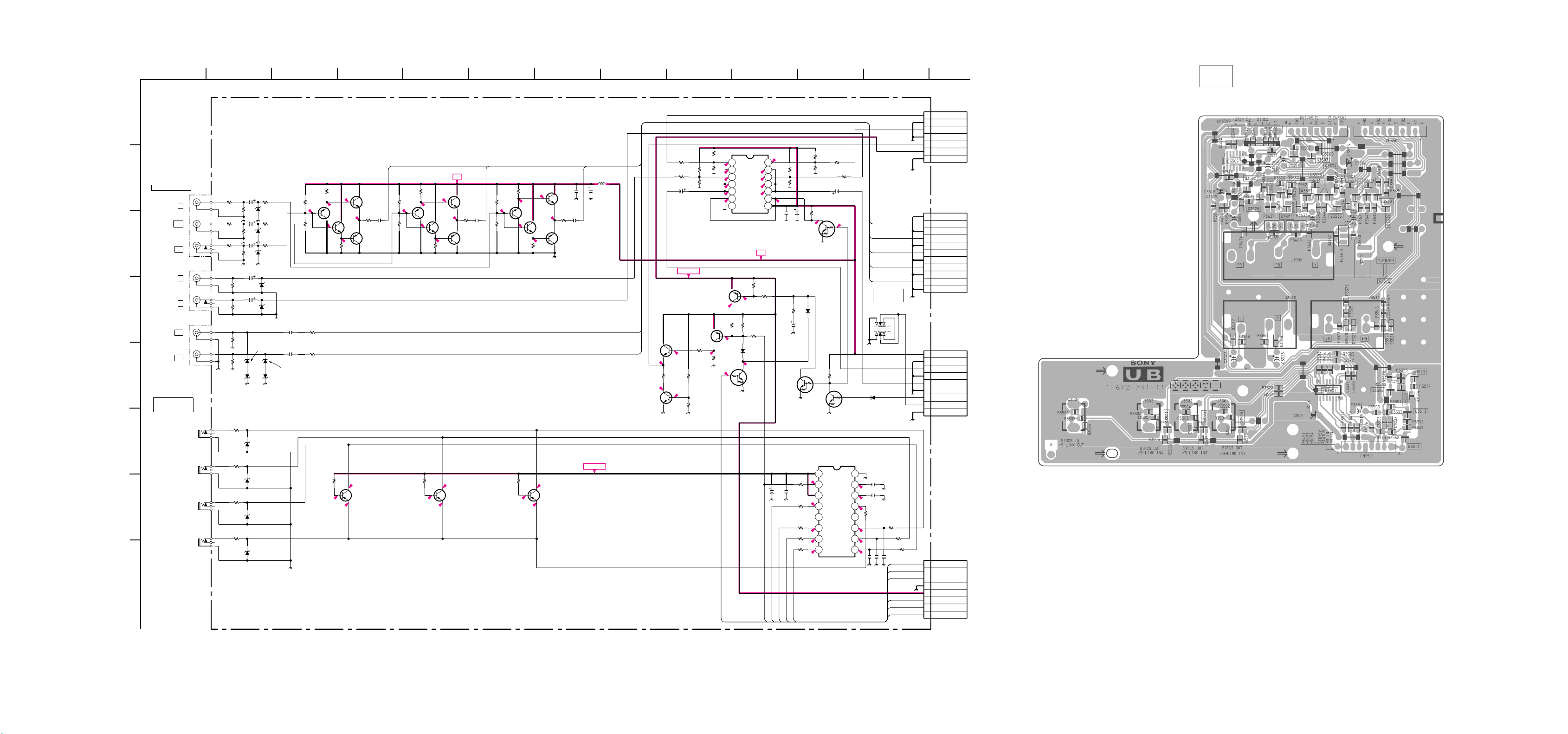
A
B
C
D
E
F
G
H
1
VIDEO 5 IN
Y
PB
PR
L
R
HD
VD
CONTROL S
/S-LINK
SIRCS OUT
/S-LINK IN1
SIRCS OUT
/S-LINK IN3
SIRCS OUT
/S-LINK IN4
SIRCS IN
/S-LINK OUT
J3509
3P
Y
PB
PR
J3510
2P
J3511
2P
J3501
JACK 3P
J3502
JACK 3P
J3503
JACK 3P
J3504
JACK 3P
2
R3667
R3630
0
75
:CHIP
:CHIP
R3668
0
:CHIP
R3669
0
:CHIP
R3634
:CHIP
R3563
470k
:CHIP
R3564
470k
:CHIP
R3566
2.2k
:CHIP
R3571
2.2k
:CHIP
D3521
UDZ-10B
R3501
22
:CHIP
R3503
22 :CHIP
R3505
22 :CHIP
R3507
22 :CHIP
C3549
47
25V
C3550
47
25V
R3632
75
:CHIP
C3551
47
25V
UDZ-10B
75
C3522
10
C3523
10
D3519
UDZ-10B
D3501
UDZ-5.6B
PROT.
D3502
UDZ-5.6B
PROT.
D3503
UDZ-5.6B
PROT.
D3504
UDZ-5.6B
PROT.
R3631
10
:CHIP
D3534
UDZ-10B
R3633
10 :CHIP
D3535
UDZ-10B
R3635
10 :CHIP
D3536
D3517
UDZ-10B
PROT.
D3518
UDZ-10B
PROT.
D3520
UDZ-10B
D3522
UDZ-10B
43
Q3528
2SB709A
PR BUFFER
R3638
1k
5.2
:CHIP
R3636
4.6 4.5
5.2
47k :CHIP
4.6
R3637
R3639
C3524
0
:CHIP
C3525
0
:CHIP
-2
47k :CHIP
1k
:CHIP
Q3529
2SD601A PR BUFFER
R3567
100
:CHIP
R3572
100
:CHIP
10k
:CHIP
4.9
UB
Q3530
2SD601A
PR BUFFER
4.6
C3552
R3640
0.47
39
16V
:CHIP
B:CHIP
Q3531
2SB709A
3.9
PR BUFFER
0
Q3501 Q3503
2SB709A
SW
0
(VIDEO INPUT,SIRCS INPUT/OUTPUT)
PR2
R3641
47k :CHIP
R3642
47k :CHIP
Q3532
2SB709A
PB BUFFER
R3643
1k
:CHIP
4.5
5.2
4.6
R3644
1k
:CHIP
Q3533
2SD601A
PB BUFFER
10k
:CHIP
4.9
5.2
4.6
3.9
2SB709A
0
9V
0
SW
PB2
Q3534
2SD601A
PB BUFFER
R3645
C3553
39
0.47
:CHIP
16V
B:CHIP
Q3535
2SB709A
PB BUFFER
R3646
47k :CHIP
R3647
47k :CHIP
Q3536
2SB709A
Y BUFFER
R3648
1k
:CHIP
5.2
4.6
R3649
1k
:CHIP
Q3537
2SD601A
Y BUFFER
R3513R3511R3509
10k
:CHIP
4.9
5.2
3.9
2SB709A
0
4.6
0
Q3505
SW
C3555
Y2
0.01
F:CHIP
Q3538
2SD601A
Y BUFFER
C3554
R3650
39
0
:CHIP
:CHIP
Q3539
2SB709A
Y BUFFER
L3503
Hm601
:CHIP
C3556
10
STBY5V
HD2
VD2
Q3510
2SD601A
BUFFER
0
0
R3543
100
:CHIP
R3544 R3545
:CHIP
R3551
100
:CHIP
C3515
1
STBY5V
Q3509
2SD601A
BUFFER
0
R3573
470
:CHIP
0.6
98765
100k
82k
:CHIP
R3552
100k
:CHIP
Q3508
2SB709A
BUFFER
R3569
4.7k
:CHIP
0
R3574
47k
:CHIP
R3577
10k
:CHIP
-2-2
R3541
82k
:CHIP
5.0
5.0
4.9
5.0
5.0
0.1
Q3513
2SB709A
BUFFER
4.8
R3594
2.2k
:CHIP
4.7
R3570
10k
:CHIP
-2
0
DTC144EKA
INVERTER
C-S
1234567
+IN1A
+IN2A
-IN2A
-IN1A
5.05.0
+IN2B
+IN1B
5.0
-IN2B
-IN1B
5.0
OUT2
OUT1
5.0
SW1
-VEE
+VCC
IC3502
BA3129F-E2
R3592
220k
:CHIP
0
R3565
47k
:CHIP
R3568
68k
:CHIP
D3532
MA111
4.8
-2
Q3514
10
SW2
9V
R3593
100k
:CHIP
C3501
SIRCS
5.0
R3546
82k
:CHIP
R3553
100k
:CHIP
0.1
8 9 10 11 12 13 14
C3518
0.01
F:CHIP
R3595
4.7k
:CHIP
C3534
C3502
0.01
F:CHIP
10
-2 -2
M1
STATUS
C3519
10
1
-2
R3515
100
:CHIP
R3516
100
:CHIP
R3517
100 :CHIP
R3518
100 :CHIP
R3519
100
:CHIP
M4
M3
11
R3542
82k
:CHIP
R3547
100k
:CHIP
R3510
100k
:CHIP
0
Q3502
DTC144EKA
D3533
MA111
Q3504
DTC144EKA
SW
NJM2145M-TE2
SIRCS I/O
12345678
VCC
4.4
SIRCS
IN4
0
STATUS
V1-S
0
V3-S
0
V4-S
0
R3548
100
:CHIP
R3554
100
:CHIP
C3516
1
4.8
SW
R3557
100k
:CHIP
Q3507
DTC144EKA
SW
IC3501
GND
INH1
INH2
TV OUT
NC
V1
V3
V4
C3528
1000p
B:CHIP
Y2
PB2
PR2
VD2
HD2
RGB/YPBPR
SW
S3501
D3505
MA111
C3503
0.001
-2
B:CHIP
-2
0.4
-2
C3504
0.001
0.4
B:CHIP
0
R3520
100
:CHIP
100 :CHIP
0
0
9 10 11 12 13 14 15 16
0
-2 -2 -2
C3526
C3527
1000p
1000p
B:CHIP
B:CHIP
B-SS609.<U/C>-UB.
12
R3521
R3522
100 :CHIP
M1
M3
M4
STATUS
SIRCS
C-S
-2
R3523
100
:CHIP
1
2
3
4
5
6
7
1
2
3
4
5
6
7
8
9
10
11
1
2
3
4
5
6
7
8
9
1
2
3
4
-2
5
6
7
8
13
CN3509
7P
YEL-L
:S-MICRO
L1
E
R1
E
SIRCS
STBY 5V
E
TO UA BOARD
CN3508
CN3504
11P
WHT-L
:S-MICRO
E
Y2
E
PB2
E
PR2
E
VD2
E
HD2
E
TO A(1/4) BOARD
CN5502
CN3502
9P
YEL-L
:S-MICRO
9V
E
L1/2
E
R1/2
E
DTV
SW2
E
TO A(1/4) BOARD
CN5504
CN3501
8P
RED-L
:S-MICRO
MBUS1
MBUS3
MBUS4
E
STBY5V
STATUS
RM IN
RM OUT
TO A(1/4) BOARD
CN526
UB
VIDEO INPUT, SIRCS
[ ]
INPUT/OUTPUT
– UB Board –
– 163 –– 162 –
– 164 –
 Loading...