

Sony KV-36FS76B Schematic

SERVICE MANUAL
AE-6A
CHASSIS
MODEL
KV-36FS76B
KV-36FS76E
COMMANDER DEST CHASSIS NO.
RM-938 FR SCC-Q83L-A
RM-938 ESP SCC-Q81N-A
MODEL
KV-36FS76U
COMMANDER DEST CHASSIS NO.
RM-938 UK SCC-Q84J-A
KV-36FS76
- 1 -
RM-938

TABLE OF CONTENTS
Section Title Page Section Title Page
Caution .................... 3
Specifications .................... 4
Connectors .................... 6
Self Diagnostic Software .................... 7
1. GENERAL
Automatically Tuning the TV .................... 10
Text .................... 10
Teletext Menu .................... 11
Multi Picture in Picture (Multi PIP) ............. 11
Picture and Picture (PAP) .................... 11
NexTView Electronic
Programme Guide (EPG) .................... 12
Using the TV menu system .................... 12
Remote Control of other equipment ............... 15
Specifications .................... 15
Troubleshooting .................... 15
2. DISASSEMBLY
2-1. Rear Cover Removal .................... 16
2-2. Speaker Disconnection .................... 16
2-3. Chassis Removal .................... 16
2-4. Service Position .................... 17
2-5. G Board Removal .................... 17
2-6. D2 Board Removal .................... 17
2-7. D1 Board Removal .................... 17
2-8. Wire Dressing 1 .................... 18
2-9. Wire Dressing 2 .................... 18
2-10. Wire Dressing 3 .................... 18
2-11. Wire Dressing 4 .................... 18
2-12. Picture Tube Removal .................... 19
Bottom Plates .................... 20
3. SET-UP ADJUSTMENTS
3-1. Beam Landing .................... 21
3-2. Convergence .................... 22
3-3. Focus Adjustment .................... 24
3-4. Screen (G2), White Balance .................... 24
4. CIRCUIT ADJUSTMENTS
4-1. Electrical Adjustments .................... 25
4-2. Volume Electrical Adjustments .................... 29
4-3. Test Mode 2 .................... 30
5. DIAGRAMS
5-1. Block Diagrams (1) .................... 31
Block Diagrams (2) .................... 32
Block Diagrams (3) .................... 33
Block Diagrams (4) .................... 34
Block Diagrams (5) .................... 35
5-2. Circuit Board Location .................... 35
5-3. Schematic Diagrams and
Printed Wiring Boards .................... 35
* A Board Schematic .................... 39
* A Board PWB .................... 36
* J2 Board Schematic .................... 43
* J2 Board PWB .................... 45
* H Board Schematic .................... 44
* H Board PWB .................... 45
* H3 Board Schematic .................... 44
* H3 Board PWB .................... 45
* F4 Board Schematic .................... 44
* F4 Board PWB .................... 45
* C Board Schematic .................... 46
* C Board PWB .................... 47
* M2 Board Schematic .................... 48
* M2 Board PWB .................... 47
* D2 Board Schematic .................... 50
* D2 Board PWB .................... 49
* D1 Board Schematic .................... 51
* D1 Board PWB .................... 52
* G Board Schematic .................... 53
* G Board PWB .................... 54
* VM Board Schematic.................... 55
* VM Board PWB .................... 54
* B5 Board Schematic .................... 55
* B5 Board PWB .................... 62
5-4. Semiconductors .................... 63
5-5. IC Blocks .................... 66
6. EXPLODED VIEWS
6-1. Chassis .................... 69
6-2. Picture Tube .................... 70
7. ELECTRICAL PARTS LIST .................... 71
ATTENTION
SHORT CIRCUIT THE ANODE OF THE PICTURE TUBE AND THE
ANODE CAP TO THE METAL CHASSIS, CRT SHIELD, OR THE
CARBON PAINTED ON THE CRT, AFTER REMOVAL OF THE
ANODE CAP.
AN ISOLATION TRANSFORMER SHOULD BE USED DURING
ANY SERVICE WORK TO AVOID POSSIBLE SHOCK HAZARD
DUE TO LIVE CHASSIS, THE CHASSIS OF THIS RECEIVER IS
DIRECTLY CONNECTED TO THE POWER LINE.
SAFETY-RELATED COMPONENT WARNING !!
COMPONENTS IDENTIFIED BY SHADING AND MARKED
THE SCHEMATIC DIAGRAMS, EXPLODED VIEWS AND IN THE
PARTS LIST ARE CRITICAL FOR SAFE OPERATION. REPLACE
THESE COMPONENTS WITH SONY PARTS WHOSE PART
NUMBERS APPEAR AS SHOWN IN THIS MANUAL OR IN
SUPPLEMENTS PUBLISHED BY SONY.
CAUTION
WARNING !!
ON
APRES AVOIR DECONNECTE LE CAP DE’LANODE,
COURT-CIRCUITER L’ANODE DU TUBE CATHODIQUE ET
CELUI DE L’ANODE DU CAP AU CHASSIS METALLIQUE DE
L’APPAREIL, OU AU COUCHE DE CARBONE PEINTE SUR LE
TUBE CATHODIQUE OU AU BLINDAGE DU TUBE
CATHODIQUE.
ATTENTION !!
AFIN D’EVITER TOUT RISQUE D’ELECTROCUTION
PROVENANT D’UN CHÁSSIS SOUS TENTION, UN
TRANSFORMATEUR D’ISOLEMENT DOIT ETRE UTILISÈ LORS
DE TOUT DÈPANNAGE LE CHÁSSIS DE CE RÈCEPTEUR EST
DIRECTMENT RACCORDÈ Á L’ALIMENTATION SECTEUR.
ATTENTION AUX COMPOSANTS RELATIFS Á
LA SECURITÈ!!
LES COMPOSANTS IDENTIFIÈS PAR UNE TRAME ET PAR UNE
MARQUE SUR LES SCHÈMAS DE PRINCIPE, LES VUES
EXPLOSÈES ET LES LISTES DE PIECES SONT D’UNE IMPOR-
TANCE CRITIQUE POUR LA SÈCURITÈ DU FONCTIONNEMENT,
NE LES REMPLACER QUE PAR DES COMPSANTS SONY DONT
LE NUMÈRO DE PIÈCE EST INDIQUÈ DANS LE PRÈSENT
MANUEL OU DANS DES SUPPLÈMENTS PUBLIÈS PAR SONY.
- 2 -
CAUTION
Lead Free Soldered Boards
The circuit boards listed below [Table 1] used in these models may
have been processed using Lead Free Solder. The boards are
identified by the LF logo located close to the board designation e.g.
F1, H1 etc [ see examples ]. The servicing of these boards requires
special precautions to be taken as outlined below.
Table 1
draoB noitcnuF
example 1
example 2
3HrossecorPkniLVA
It is strongly recommended to use Lead Free Solder material in order to guarantee optimal quality of new solder joints. Lead Free Solder is
available under the following part numbers :
rebmuntraP retemaiD skrameR
91-500-046-7mm3.0gK52.0
02-500-046-7mm4.0gK05.0
12-500-046-7mm5.0gK05.0
22-500-046-7mm6.0gK52.0
32-500-046-7mm8.0gK00.1
42-500-046-7mm0.1gK00.1
52-500-046-7mm2.1gK00.1
62-500-046-7mm6.1gK00.1
Due to the higher melting point of Lead Free Solder the soldering iron tip temperature needs to be set to 370 degrees centigrade. This requires
soldering equipment capable of accurate temperature control coupled with a good heat recovery characteristics.
For more information on the use of Lead Free Solder, please refer to http://www.sony-training.com
- 3 -
LEDOMMETI metsySnoisiveleT metsySoeretS egarevoClennahC metsySroloC
BL,I,K/D,H/G/B
EH/G/B
MACIN/NAMREG
oeretS
MACIN/NAMREG
oeretS
02S-10S:VTELBAC
14S-12S:REPYH
30S-10S,21R-1R,21E-2E:FHV
96R-12R,96E-12E:FHU
02S-10S:VTELBAC
14S-12S:REPYH
Q-B,01F-20F,30S-10S,21R-1R,21E-2E:FHV
96R-12R,96B-12B,96F-12F,96E-12E:FHU
MACES,LAP
85.3CSTN,34.4CSTN
)NIOEDIV(
MACES,LAP
85.3CSTN,34.4CSTN
)NIOEDIV(
UI
ebuTerutciP
.)yllanogaid
]RAER[slanimreTtuptuO/tupnI snoitacificepSlareneG
rotcennocoruEnip-12:1
)dradnatsCELENEC(
rotcennocoruEnip-12:2
rotcennocoruEnip-12:3
rotcennocoruEnip-12:4
skcaJonohPoiduArofelbairavsrotcennoCtuptuO
]TNORF[slanimreTtuptuO/tupnI lortnoCderarfnI:metsySlortnoCetomeR
kcajenohpdaeHkcajinimoerets
stupnioiduAskcajonohp
stupnioediVskcajonohp
tupnioediVSNIDnip4
.BGRrofstupnI
.slangis
.BGRrofstupnI
)tuOrotinoM(
)elbatceles(
.slangiS
MACIN
oeretS
nortinirTDFyalpsiDtalF
)sehcni63(mc29xorppA
derusaemerutcipmc88xorppA(
.slangisoediVdnaoiduArofstupnI
oiduAdnaoediVVTfostuptuO
.slangisoediVdnaoiduArofstupnI
.slangisoiduAdnaoediVVTfostuptuO
.slangisoediVdnaoiduArofstupnI
.oediVSrofstupnI
.slangisoiduAdnaoediVVTfostuptuO
.slangisoediVdnaoiduArofstupnI
.oediVSrofstupnI
96B-12B:FHU
tuptuodnuoS
rekaepstfeLdnathgiR
refooWbuS
stnemeriuqeRrewoPV042-022
noitpmusnoCrewoPW661
snoisnemiDmm195x416x279xorppA
thgieWgk0.09xorppA
seirosseccAdeilppuS
serutaeFrehtO
.srenuT
cdV3
stnemeriuqerrewoP
)AAezis(6R
.ecitontuohtiwegnahcottcejbuserasnoitacificepsdnangiseD
MACES,LAP
85.3CSTN,34.4CSTN
)NIOEDIV(
)SMR(W01x2)rewoPcisuM(W02x2
)SMR(W51x1)rewoPcisuM(W03x1
)1(rednammoCetomeR839-MR
)2(yrettab6RdetangisedCEI
,erutciPdnaerutciPcimanyD,FCD,FMCRD
2,ybloDlautriV,noitcudeResioNotuA
noitangisedCEIseirettab2
- 4 -
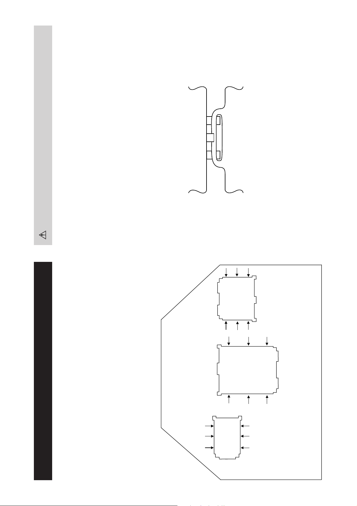
How to replace the fuse.
Open the fuse compartment with
a screwdriver blade and replace
the fuse.
FUSE
metI
emaNledoM
PAPFFOFFOFFO
PIPFFOFFOFFO
ytiroirPBGRNONONO
xoBrefooWNONONO
1tracSNONONO
2tracSNONONO
)3(nitnorFNONONO
4tracSNONONO
rotcejorPFFOFFOFFO
G/BmroNNONOFFO
ImroNNOFFONO
K/DmroNNONOFFO
SUAmroNFFOFFOFFO
LmroNNOFFOFFO
TASmroNFFOFFOFFO
MmroNFFOFFOFFO
txeteleTNONONO
oeretSmaciNNONONO
B67SF63-VK E67SF63-VK U67SF63-VK
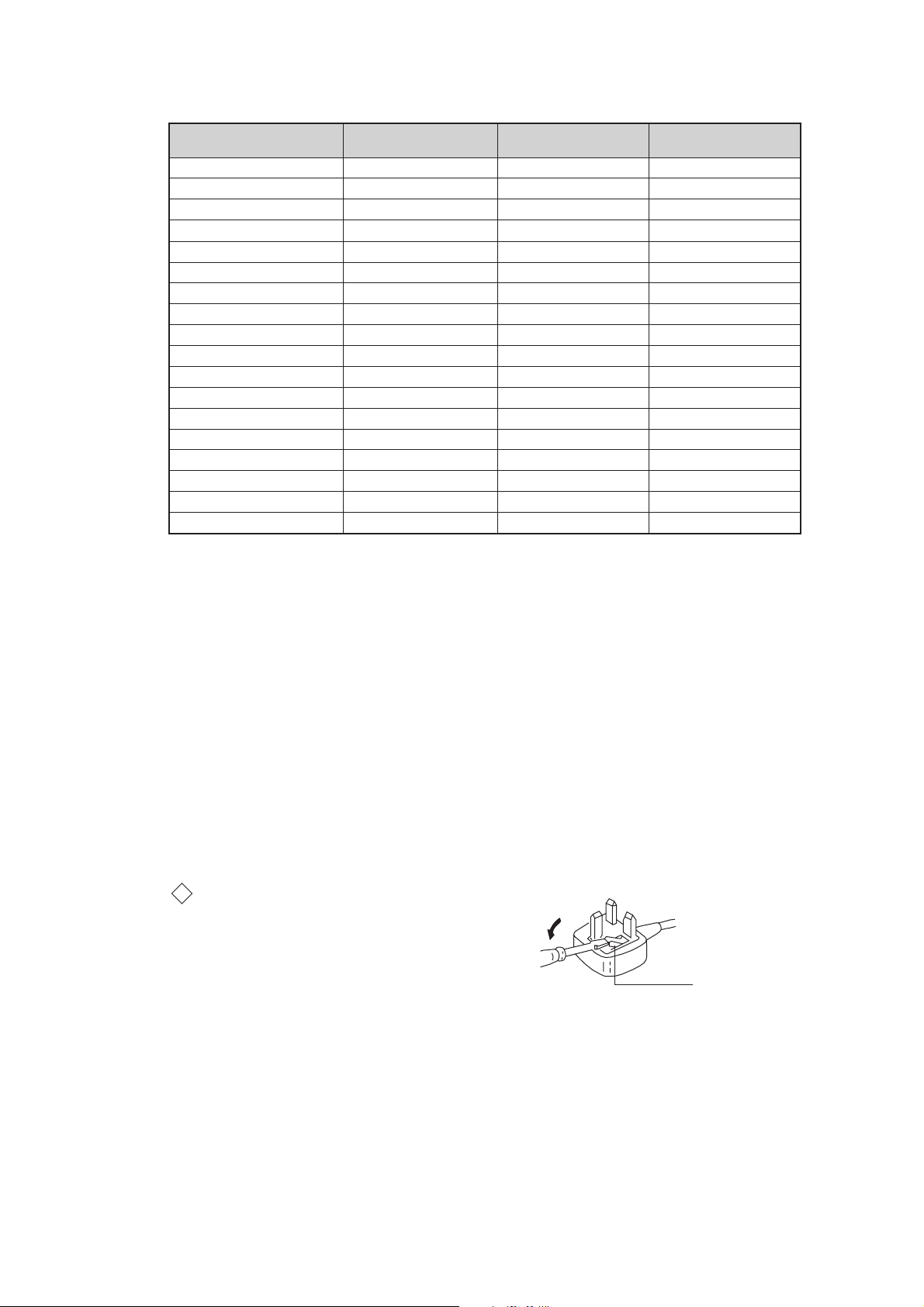
WARNING (UK Models only)
The flexible mains lead is supplied connected to a B.S. 1363 fused
plug having a fuse of 5 AMP rating. Should the fuse need to be
replaced, use a 5 AMP FUSE approved by ASTA to BS 1362, ie one
that carries the
IF THE PLUG SUPPLIED WITH THIS APPLIANCE IS NOT SUITABLE FOR THE OUTLET SOCKETS IN YOUR HOME, IT SHOULD
BE CUT OFF AND AN APPROPRIATE PLUG FITTED. THE PLUG
SEVERED FROM THE MAINS LEAD MUST BE DESTROYED AS A
PLUG WITH BARED WIRES IS DANGEROUS IF ENGAGED IN A
LIVE SOCKET.
When an alternative type of plug is used, it should be fitted with a
5 AMP FUSE, otherwise the circuit should be protected by a 5 AMP
FUSE at the distribution board.
ASA
mark.
T
- 5 -
21 pin connector
21
19
17
15
13
11
9
7
5
3
1
20
18
16
14
12
10
8
6
4
2
Pin No 1 2 4 Signal Signal level
1 Audio output B
2
3
4 Ground (audio)
5 Ground (blue)
6 Audio input A
7 Blue input 0.7 +/- 3dB, 75 ohms positive
8 Function select
9 Ground (green)
10 Open
11 Green Green signal : 0.7 +/- 3dB, 75 ohms,
12 Open
13 Ground (red)
14 Ground (blanking)
15
16 Blanking input
17 Ground (video
18 Ground (video
19 Video output 1V +/- 3dB, 75ohms, positive sync 0.3V
20
21 Common ground
3
(right)
Audio input B
(right)
Audio output A
(left)
(left)
(AV control)
_ _ Red input 0.7 +/- 3dB, 75 ohms, positive
_ (S signal Chroma
input)
(Ys signal)
output)
input)
_ _ Video input 1V +/- 3dB, 75ohms, positive sync 0.3V
_ Video input
Y (S signal)
(plug, shield)
Standard level : 0.5V rms
Output impedence : Less than 1kohm*
Standard level : 0.5V rms
Output impedence : More than 10kohm*
Standard level : 0.5V rms
Output impedence : Less than 1kohm*
Standard level : 0.5V rms
Output impedence : More than 10kohm*
High state (9.5-12V) : Part mode
Low state (0-2V) : TV mode
Input impedence : More than 10K ohms
Input capacitance : Less than 2nF
positive
0.3 +/- 3dB, 75 ohms, positive
High state (1-3V) Low state (0-0.4V)
Input impedence : 75 ohms
(-3+10dB)
(-3+10dB)
1V +/- 3dB, 75ohms, positive sync 0.3V
(-3+10dB)
Connected Not Connected (open) * at 20Hz - 20kHz
Rear Connection Panel Front Connection Panel
S-Video
socket
niP
oN
1dnuorG-
2dnuorG-
3tupni)langisS(Y,mho57Bd3-/+V1
4tupni)langisS(CBd3-/+V3.0
langiS leveLlangiS
noitarugifnocniptekcosoediVS
V3.0.cnySevitisop
Bd01+3-
evitisop,mho57
.cnyS
- 6 -
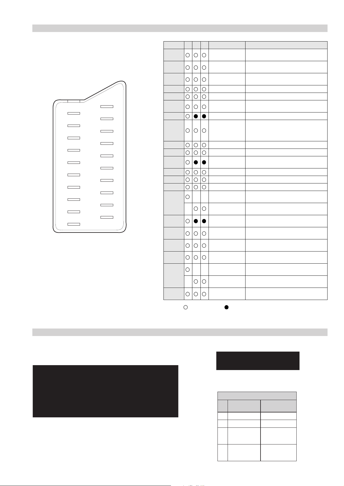
AE-6A SELF DIAGNOSTIC SOFTWARE
The identification of errors within the AE-6A chassis is triggered in one of two ways :- 1: Busy or 2: Device failure to respond to IIC. In the
event of one of these situations arising the software will first try to release the bus if busy (Failure to do so will report with a continuous
flashing LED) and then communicate with each device in turn to establish if a device is faulty. If a device is found to be faulty the relevant
device number will be displayed through the LED (Series of flashes which must be counted) See table 1., non fatal errors are reported using this
method.
metIcitsongaiD
noitpircseD
nonruttonseodrewoPthgiltonseoD
)PCO(tnerrucrevOB+semit2
deppotsnoitcelfeDlacitreVsemit4
ybdnatSsemitfooN
sehsalFDEL
.tiucricneposiesuF
egasseMrorrE
devreseR 10
)noitcetorPtnerruCrevO(PCO 20
)noitcetorPegatloVrevO(PVO 30
noitcetorPlacitreV 40
noitcetorPlatnoziroH 60
noitcetorPrekaepS 70
rorrEsuBC2I 80
MVN,23C42TS.B-2M 90
draoB-A 01
draoB5B 11
draoB2J 21
draoBH 31
draoBSM 41
redoceDruoloCniaM.B-5B 51
dnekcaB,Q0512AXC.B-A 61
.corPdnuoS,1143PSM.B-A 71
desutoN 23-81
esuacelbaborP
noitacoL
.nideggulptonsidrocrewoP
)draoB1D(.detrohssi)3018/2018Q(TUO.H
)draoB1D(.detrohssi)6018Q(TEFytiraeniL
)draoB1D(.detrohssiCIrewoP1088CI
)draoB1D(nepo7028RdeilppustonsiV51+
)draoB1D(nepo6028RdeilppustonsiV51-
)draoBA(detrohssi1071CI
)edoMnoitcudorPnidelbasid,s03retfastratskcehc(BKAelbatsnU 50
smotpmySdetceteD
noemoctonseodrewoP
VTehtotdeilppussirewopoN
ytluafsiylppusrewopCA
noemoctonseodrewoP
detrohssahenilrewopnodaoL
deppotssaheslupnoitcelfedlacitreV
detrohssahenilrewoP
DEL
edoC
Flash Timing Example : e.g. error number 3
StBy LED
ON ON ON
OFF
- 7 -
OFF

Error Detection Monitor
Device acknowledge is used to check IIC errors. Device acknowledge is checked by sending an IIC start sequence during CRT power on. Each
device is checked three times, if there is no acknowledge after each attempt, it will be regarded as an error.
There are three steps to check for errors.
1. IIC line 0
If all devices except the NVM have errors, IIC line 0 error is displayed.
2. Board check
If all devices mounted on one board have errors, board error is displayed.
3. Each device check
If IIC line error and board error are not detected then the device with the error is displayed.
The detected errors can be displayed as follows :
1. Error Monitor Menu.
2. Error Reader.
1. Error Monitor Menu
ERROR MONITOR
1. IGNORE ERRORS OFF ON OFF
Operating Time : 000167 h 45 min
Stored Errors :
1. A - B TU1350 Sub-Tuner
2. J - B TDA9320 Sub Col. Dec.
3. No Error Occured
4. No Error Occured
5. No Error Occured
Current Error :
A - B TU1350 Sub-Tuner
Last menu Enter item
- 8 -
2. Error Reader Display
The error reader display is connected to the service connector to read actual error codes. The part number for the error reader display is
S-188-900-10. Once an error has been detected it will then be displayed on the two digit error reader. The errors displayed refer to the following
table.
edoCrorrE egasseMrorrE
h000deruccOrorrEoN
h1000C2I,rorrEsuB
h2001C2I,rorrEsuB
h3002C2I,rorrEsuB
h001draoB-A
h101.pxEtroP,5781AXC.B-A
h201renuT-niaM,xx06UT.B-A
h301FIniaM,6889ADT.B-A
h401dnekcaB,Q0512AXC.B-A
h501CAD,14188BM.B-A
h601.corPdnuoS,G1143PSM.B-A
h701.vnoC.anyD,0708AXC.B-A
h002draoB-5B
h102redoceDruoloCniaM.B-5B
h202redoceDruoloCbuS.B-5B
h302XDIM.B-5B
h402yarrAetaGamaronaP.B-5B
h502noitcudeResioN.giD.B-5B
h003draoB-H
h103kniLVA,8802DXC.B-H
h004draoB-J
h104hctiwSVA,5581AXC.B-2J
h204hctiwSVA,9412AXC.B-2J
h304renuT-buS,xx06UT.B-2J
h404FIbuS,6889ADT.B-2J
h005draoB-2M
h105MVN,23C42TS.B-2M
h006draoB-1SM
h106kcitSyromeM.B-1SM
- 9 -

SECTION 2 DISASSEMBLY
2-1. Rear Cover Removal 2-2. Speaker Connector Disconnection
=>
=>
=>
=>
=>
Remove the rear cover fixing screws indicated. Take care
when removing the rear cover not to damage the speaker
cables [Disconnect the speaker connector] as speakers are
fitted inside the rear cover.
=>
=>
=>
<=
<=
<=
=>
=>
=>
Before completely removing the rear cover disconnect the
speaker connector which is located on the inside.
2-3. Chassis Removal and Refitting
To remove lift the main bracket rear slightly and slide the
chassis away from the beznet. Ensure that the interconnecting
leads are released from their purse locks to prevent damage
being caused.
When refitting the chassis ensure that the main bracket is
located in the beznet guide slots before sliding the chassis
forwards. Refit the inter-connecting leads in their respective
purse locks.
- 16 -
2-4. Service Position 2-5. G Board Removal
Screw
Clips
To place the chassis in the service position, remove the D2
bracket (see 2-7.) and locate on the beznet inside the set.
Insert the main bracket firmly into the T-slot located on the left
corner of the beznet as indicated (see inset). To gain access to
the underside of the boards follow the instructions on page 19.
[Removal and Replacement of the main bracket bottom plates].
2-6. D2 Board Removal
To remove the G Board first remove the PFC bracket by
removing the two fixing screws (one on each side of the
bracket) and lifting away from the G board.
Remove the screw from the centre of the G board, release
the clips circled and ease the board gently away from the
support bracket.
2-7. D1 Board Removal
Screws
Clips
To remove the D2 board remove the two screws circled,
release the clips circled and ease the board gently away from
the support bracket.
Screws Clips
To remove the D1 board first remove the D2 bracket by
removing the three screws from the bracket (one on opposite
side) and releasing the four clips (two on each side of the
bracket). The D1 board can then be removed using the
same method as the G board.
- 17 -

2-8. Wire Dressing 1
2-9. Wire Dressing 2
20mm
20mm
Ensure that wires do not touch heatsinks and high temperature
hotspots. All wires must be kept at a minimum distance of
20mm away from the EHT lead
2-10. Wire Dressing 3
The sheathed end of the ground connecting lead must be
plugged into the F3 board to avoid the possibility of the AC
mains power touching ground.
2-11. Wire Dressing 4
Ensure the RF lead is dressed as shown circled above to avoid
obstructing the rear cover.
To avoid damage to the ground interconnecting leads from the
sharp edges of the heatsink they must be dressed as shown
above between the rear of the heatsink and the tuner.
- 18 -
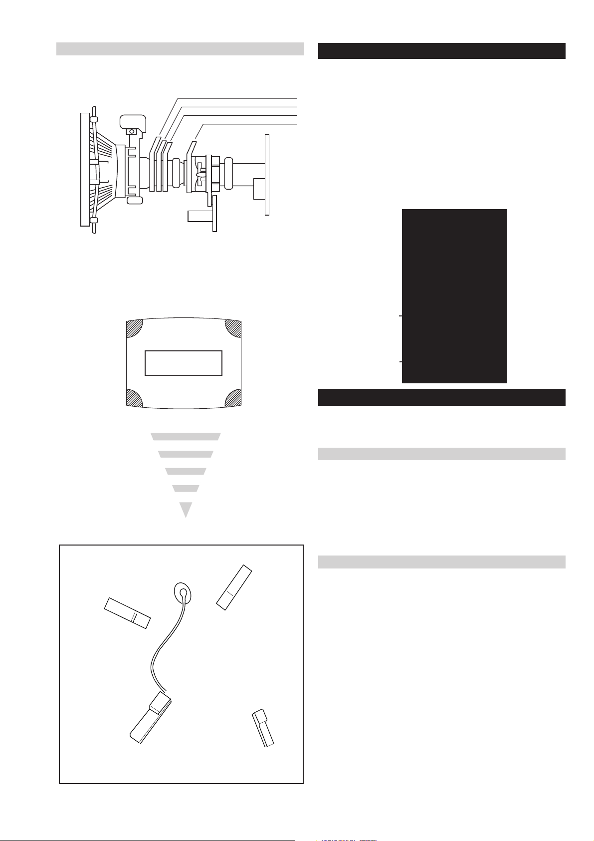
2-12. Picture Tube Removal
WARNING:
BEFORE REMOVING
THE ANODE CAP
High voltage remains in the CRT even
after the power is disconnected. To
avoid electric shock, discharge CRT
before attempting to remove the anode
cap. Short between anode and CRT
coated earth ground strap.
Coated Earth
Ground Strap
10
8
7
6
5
4
9
1
3
2
1. Discharge the anode of the CRT and remove the anode cap.
2. Unplug all interconnecting leads from the Deflection yoke, neck
assy, degaussing coils and CRT grounding strap.
3. Remove the C Board from the CRT.
4. Remove the chassis assembly.
5. Loosen the Neck assembly fixing screw and remove.
6. Loosen the Deflection yoke fixing screw and remove.
7. Place the set with the CRT face down on a cushion and remove
the Degaussing Coil holders.
8. Remove the Degaussing Coils.
9. Remove the CRT grounding strap and spring tensioners.
10. Unscrew the four CRT fixing screws [ located on each CRT
corner ] and remove the CRT.
[Take care not to handle the CRT by the neck.]
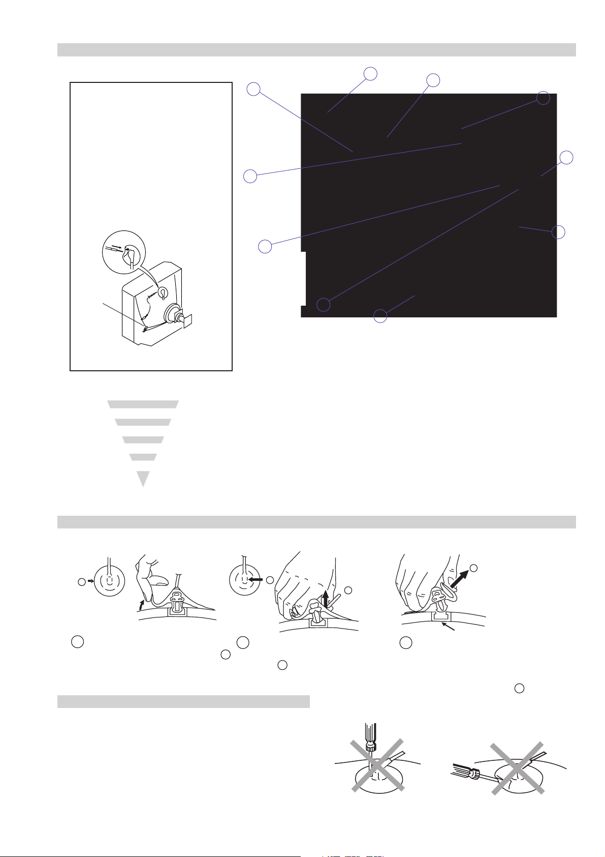
Removal of the Anode-Cap
REMOVAL PROCEDURE.
a
1
Turn up one side of the rubber cap in
the direction indicated by the arrow a
b
2 Using a thumb pull up the rubber cap
firmly in the direction indicated by the
arrow b
How to handle the Anode-Cap
1. To prevent damaging the surface of the anode-cap do not use
sharp materials.
2. Do not apply too great a pressure on the rubber, as this may cause
damage to the anode connector.
3. A metal fitting called a shatter hook terminal is fitted inside the
rubber cap.
4. Do not turn the rubber foot over excessively, this may cause
damage if the shatter hook sticks out.
c
b
Anode button
3 When one side of the rubber cap is
separated from the anode button, the
anode-cap can be removed by turning
up the rubber cap and pulling it up in
the direction of the arrow c
- 19 -
Catch
For safety reasons, on no account should the plates be removed
and not refitted after servicing.
Because the plates differ in size it is important that the correct plates are refitted in their original
location.
Please note that the plates need to be rotated 180 degrees from their cut position to allow the
(2) REFITTING THE PLATES
tabs to be fitted into their catch positions.
Ta b
REMOVAL AND REPLACEMENT OF THE MAIN-BRACKET
BOTTOM PLATES.
Only remove the necessary plate to gain access to the printed wiring board.
In the event of servicing being required to the solder side of the A, D1 or G printed wiring
boards, the bottom plates fitted to the main chassis bracket require to be removed.
This is performed by cutting the gates with a sharp wire cutter at the locations indicated by the
arrows.
(1) REMOVING THE PLATES
Note : There are 3 plates fitted to the main bracket and secured by 3 gates.
- 20 -
SECTION 3 SET-UP ADJUSTMENTS
Neck assy
G2
G1
+
Align the edge
of the neck assy on the
edge of the G3 grid closest
to the G2 grid.
G3
• When complete readjustment is necessary or a new picture tube
is installed, carry out the following adjustments.
• Unless there are specific instructions to the contrary, carry out
these adjustments with the rated power supply.
• Unless there are specific instructions to the contrary, set the
controls and switches to the following settings :
Contrast .................................. normal
Brightness .................................. normal
3-1. Beam Landing
Preparation :
1. In order to reduce the influence of geomagnetism on the set’s
picture tube, face it in an easterly or westerly direction.
2. Switch on the TV set’s power and degauss with a degausser.
(1) Adjustment of Correction Magnet for Y-Splitting Axis.
1. Input a crosshatch signal from the pattern generator.
2. Set the Picture control to minimum and confirm that the
Brightness control is set to normal.
3. Position the neck assembly as indicated in Fig.3-3.
4. Loosen the deflection yoke fixing screw.
5. Move the deflection yoke as far forward as is possible.
6. Adjust the upper and lower pin symmetrically by opening or
closing the Y-splitting axis correction magnets located on the
neck assembly. [See Fig 3-2]
7. Return the deflection yoke to its original position and re-tighten
its fixing screw.
Fig.3-1
Y-splitting axis correction magnet
Carry out the adjustments in the following order :
3-1. Beam Landing and Geometry.
3-2. Convergence.
3-3. Focus.
3-4. White Balance.
Note : Test equipment required.
1. Color bar/pattern generator.
2. Degausser.
3. Oscilloscope.
4. Digital multimeter.
(2) Landing and Geometry
Note : Before carrying out the following adjustments adjust the
magnets as indicated on page 22 [See Fig.3-4].
1. Input a crosshatch signal from the signal generator.
2. Rough-adjust the focus and horizontal convergence.
3. Switch from the crosshatch pattern to an all-red pattern.
4. Move the deflection yoke backwards and adjust with the purity
magnet so that the red is at the centre and it aligns
symmetrically [See Fig.3-5].
5. Move the deflection yoke forward to the point where the entire
screen just becomes red [Mark its position].
6. Move the deflection yoke further forward until the screen just
changes colour at the edges. [Mark its position].
7. Position the deflection yoke between the two marks indicated
above.
8. Input a crosshatch pattern from the pattern generator and rotate
the deflection yoke so that the horizontal lines are parallel with
the top and bottom of the screen.
9. When the position of the deflection yoke has been determined,
fasten it with its fixing screw.
10. Once dy rotation and swing left and right for h linearity is ok on
cross hatch pattern, insert dy wedges. [See Fig.3-6].
11. Switch the pattern generator to green then blue and confirm the
purity.
12. If the beam does not land correctly in all the corners of the
screen, use disk magnets to correct it. [Confirm the corner
landing forgreen and blue].
13. Re-check geometry for landing magnet effect. Adjust using
deflection menu. [TT Mode].
Fig.3-2
Caution :
High voltages are present on the Deflection yoke terminals - take care
when handling the Deflection yoke whilst carrying out adjustments.
Fig.3-3
- 21 -
Fig.3-4
B
G
R
B
G
R
Purity magnets
Align pips on
each magnet
Align both Purity
magnets to the vertical
position
Purity control magnets
3-2. Convergence
(1) Screen centre convergence [Static convergence]
Fig.3-5
GREEN
RED
BLUE
Disk magnets or
rotatable disk
Purity control corrects
this area
magnets correct
these areas (a-d)
ab
c
Deflection yoke positioning
corrects these areas
d
1. Input a dot pattern signal from the pattern generator.
2. Normalize the picture setting.
3. [Moving vertically], adjust the V.STAT magnet so that the
vertical red, green and blue dots coincide at the centre of the
screen.
Center dot
H.STAT
convergence
Vertical Static Magnet
V.STAT
control
RV5375 (H STAT)
H STAT Convergence
(on mount side)
Disk Magnets
Fig.3-6
5 Wedges
required
By opening or closing the V.STAT magnet, the red green and
blue dots move in the direction indicated below.
Note: Do not adjust the H.STAT by rotating the V.STAT
magnets as this can affect the focus setting.
- 22 -
4. Correction for HMC [Horizontal mis-convergence] and VMC
+
+
+
YCH VR
Deflection Yoke
+
+
+
TLV VR
Deflection Yoke
[Vertical mis-convergence] by using the BMC [Hexapole]
magnet.
a). HMC correction by BMC [Hexapole] magnet and movement of
the electron beam.
HMC correction(A) HMC correction(B)
A < B
RG B
A > B
RGB
HTIL correction can be performed by adding a THL correction
assembly to the Deflection yoke.
A = B
A B
RG B
A B
A = B
A B
RG B
A B
b). VMC correction by BMC [Hexapole] magnet and movement of
the electron beam.
VMC correction(A) VMC correction(B)
C < D
C
D
C = D C > D C = D
R
G
B
R
C
G
D
B
C
D
R
G
B
R
C
G
D
B
HAMP Adjustment
YCH Adjustment
TLV Adjustment
Adjust the HAMP using HAMPL and HAMPR registers in the
Dynamic Convergence section of the service menu.
HTIL Adjustment
THL Correction assy
H-TRAP Adjustment
+
+
HTRAP VR
+
Deflection Yoke
The H-TRAP should not be adjusted unless absolutely necessary as it
affects the TLV settings.
- 23 -
Layout of each control
Purity magnet
BMC (Hexaploe) magnet
V STAT convergence magnet
Y-splitting axis correction magnet
Note : If you are unable to adjust the corner convergence properly,
this can be corrected with the use of permalloy magnets.
a
b
3-3. Focus Adjustment
1. Receive a cross hatch pattern from a video generator.
2. Adjust the focus control located on the flyback transformer to
the best level at the centre of the screen.
3. Check left and right x-axis vertical line thickness and adjust to
make them as thin as possible.
4. Considering x-axis and centre, adjust to make uniform.
5. If no cross hatch signal is possible, follow the next three steps.
6. Receive a television broadcast signal.
7. Normalize the picture setting.
8. Adjust the focus control located on the flyback transformer to
obtain the best focus at the centre of the screen.
Bring only the centre area of the screen into focus, the magentaring appears on the screen. In this case, adjust the focus to
optimize the screen uniformly.
Focus
a-d: screen-corner
convergence defect
c
Install the permalloy assembly
for the area that needs correcting.
b
Permalloy Assy
X-4387-214-1.
d
Convergence adjustment with permalloy
Screen
d
3-4. Screen (G2), White Balance
[Adjustment in the service mode using the remote
commander]
G2 adjustment
1. Input a dot signal from the pattern generator.
2. Set the Picture, Brightness and Colour to minimum.
3. Apply 165V DC from an external power supply to the R, G
and B cathodes of the CRT.
4. Whilst watching the picture, adjust the G2 control [SCREEN]
located on the flyback transformer to the point just before the
flyback return lines disappear.
a
White balance adjustment for TV mode
1. Input an all-white signal from the pattern generator.
2. Program the Remote Commander for operation in Service Mode.
[See Page 25].
3. Enter into the ‘Service Mode’ by pressing ‘VIDEO’ button twice
and ‘MENU’ on the Service Commander.
4. Select ‘Device Register Setting’ from the on screen menu display
and press ‘Right Arrow’.
5. Select ‘Backend’ from the on screen menu display and press
‘Right Arrow’.
6. Set the ‘Contrast’ to MAX.
7. Set the ‘R-Drive’ to 45.
8. Adjust the ‘G-Drive’ and the ‘B-Drive’ so that the white
balance becomes optimum.
9. Press the ‘OK’ button to write the data for each item.
10. Set the ‘Contrast’ to MIN.
11. Set the ‘R-Cutoff’ to 35.
c
12. Adjust the ‘G-Cutoff’, and the ‘B-Cutoff’ with the left and
right buttons on the remote commander so that the white
balance becomes optimum.
13. Press the ‘OK’ button to write the data for each item.
- 24 -
SECTION 4 CIRCUIT ADJUSTMENTS
4-1. Electrical Adjustments
Service adjustments to this model can be performed using the
supplied remote Commander RM-938.
Programming the Remote Commander for Operation in Service Mode
1. Press the VCR/TV/DVD button until the
TV LED lights.
2. Press and hold the yellow button for
approx. 5 seconds until the TV LED
flashes quickly.
3. Press 99999. All three LED’s should light.
The remote commander is now set to Service Mode.
4. To return the remote commander to normal operation mode
repeat steps 1. and 2. then press 00000. All three LED’s
should light.
The remote commander is now set to normal mode.
Setting the TV into Service Mode
1. Program the remote commander for operation in Service
Mode as described above.
2. Turn on the TV main power switch.
3. Press the video standby button on the remote
commander twice.
‘TT ’ will appear in the upper right corner of the screen.
Other status information will also be displayed.
Initialising Menu
gnisilaitinI
gnitteSledoM
gnitteSnoitanitseD
gnitteScisaB
gnitteSerutaeF
:tceleS:unemtxeN
Model Setting
The menu contains a list with all the available models of this software
to set up the TV set in an easy way. The selection of a model is setting
data for its features and hardware resources which cannot be detected
by the automatic power on H/W detection as well as a special model
byte to get an unique model identification for models which cannot be
differed by features and hardware resources (e.g. KV-29FQ76 and
KV-32FQ80)
Before data is set, the user will be asked if he really wants to set a
new model. If the user agrees, automatically the destination setting
menu is shown.
gnitteSledoM
67QF92-VK
67QF92-VK
08QF63-VK
67SF63-VK
eseR
t
4. Press ‘MENU’ on the remote commander twice to obtain the
following menu on the screen.
71095V,200201rpA,A6EAecivreS
gnisilaitinI
seciveDteseR
gnirotinoM
gnitteSretsigeReciveD
.tnemtsujdAlaicepS
:uneMtxeN:tceleS
5. Move to the corresponding adjustment item using the
up or down arrow buttons on the Remote Commander.
6. Press the right arrow button to enter into the required menu item.
7. Press the ‘Menu’ button on the Remote Commander to quit the
Service Mode when all adjustments have been completed.
Note :
· After carrying out the service adjustments, to prevent the
customer accessing the ‘Service Menu’ switch the TV set
OFF and then ON.
· Certain menu items are only available in production mode.
KCALBytimrofnoCoN=
NEERGledoMelbitapmoC=
DERatadllarofytimrofnoC=
Table.4-1
Indication of Model Compatibility.
Black:
If any data does not match to specific model, the model name is
displayed in black.
Green:
All data which is checked by model setting menu concurs to model
except model byte.
Red:
All data which is checked by model setting menu concurs to model
including model byte.
Note:
After selecting a model, it may be necessary to reset some devices to
get the correct data. (Treble/Bass Offset of Sound, deflection
adjustments, ...)
- 25 -
Basic Setting
noitcelfeD.txE
oNrcseDfeDniMxaMataD
1esahPFD5810552581
2esahPPQD5210552521
3raeniLdiM5310552531
4raeniLH0010552021
5pmacaPQD0510552231
6lvlcdPQD8410552621
7"63tneCH0055208
X-diM
oNrcseDfeDniMxaMataD
1SOPHM061-610
2SOPHS08-80
3LESSYD1031
4YALEDSYD7077
5DOMCNYSDNOFFONONO
6prahStxeTFFOFFONOFFO
7LLP.txEFFOFFONOFFO
8retliFHFFOFFONOFFO
hctiwSoediV/oiduA
gnittescisaB
oNrcseDniMxaMataD
1G/B.sySFFONONO
2K/D.sySFFONONO
3L.sySFFONOFFO
4)KU(I.sySFFONOFFO
5)LRI(I.sySFFONOFFO
6noitpo.taNTXT143
7TRC9:61FFONOFFO
8refoow-buSFFONONO
9yb-dnatsotuAFFONONO
01retlif-bmoCFFONONO
11tedCYotuAFFONONO
21tedbmocotuAFFONONO
31elbaliavA2VAFFONONO
41elbaliavA3VAFFONONO
51elbaliavA4VAFFONONO
61elbaliavA5VAFFONONO
71epaTMACESFFONOFFO
81etuMdnuoS1VAFFONONO
Table.4-2
Feature Setting
gnitteserutaeF
oNrcseDniMxaMataD
1PAPFFONONO
2TAPFFONONO
3XEDNIFFONONO
4txeTeleTFFONONO
5GPEFFONONO
6beWeleTFFONOFFO
Table.4-3
oNrcseDfeDniMxaMataD
11TUOVC0090
22TUOVC2090
3LRTC0OLFFOFFONOFFO
4LRTC1OLFFOFFONOFFO
51TUOCY2072
62TUOCY0070
7WSDCZFFOFFONOFFO
8ETUM3TUOAFFOFFONOFFO
91TUOA3073
012TUOA1071
11LEDPUORG6101361
213TUOA3073
31CLOV3TUOA4074
41FLOV3TUOA4074
51R/L3TUOA0030
61WS1DGNOFFONONO
71WS2DGNOFFONONO
811CNYS1011
912CNYS1011
021TNOCS3233
121OEDIV4034
221OIDUA0030
322TNOCS2232
422OEDIV4034
522OIDUA0030
623TNOCS2232
723OEDIV0030
823OIDUA1031
Table.4-5
Device Register Setting
dnekcaB
noitcelfeD
noitcelfeDtxE
ecnegrevnoCcimanyD
1redoceDruoloC
2redoceDruoloC
hctiwSoediV/oiduA
X-diM
X-diMLLPlanretxE
dnuoS
RNlatigiD
Table.4-4
Table.4-6
Table.4-7
- 26 -

1redoceDruoloC
)tnoc(1redoceDruoloC
oNrcseDfeDniMxaMataD
753EDOMDCFFOFFONOFFO
85SOPSH50515
95DNLRHTNFFOFFONOFFO
06VELECILS00130
16AERAPUFFOFFONOFFO
26NIHTPUFFOFFONOFFO
36J941XFFOFFONOFFO
46CTSMDFFOFFONOFFO
56TSNIFFOFFONOFFO
66LVLRPUNOFFONONO
76LVLSFOFFOFFONOFFO
86TSFOLSFFOFFONOFFO
9634MORF2032
07EDIWMORF2032
17SELTITRF2032
27LFPLNOFFONONO
37TESERWAFFOFFONOFFO
471EPOLSOTD005520
572EPOLSOTD005520
673EPOLSOTD005520
77CNACPUTES00510
87TNIV70517
97HPPLCTXE00360
08TUOTSETFFOFFONOFFO
18METSYSLOC80518
28EDOMBGR2032
38LESSYFFOFFONOFFO
48TEDNFFOFFONOFFO
58ECNAHNEV4074
68RNPFFOFFONOFFO
78QERFV0030
88BMOCNFFOFFONOFFO
98WSOTUAFFOFFONOFFO
09PARTMACESFFOFFONOFFO
19EDOMLLEBFFOFFONOFFO
29LIKMACES1031
39SOPDI2032
49DIWDINOFFONONO
59SYSLOC-EFFOFFONOFFO
69TUPNI-EFFOFFONOFFO
79KCOLH-EFFOFFONOFFO
89QERFV-ENOFFONONO
99SSW-EFFOFFONOFFO
001TESERTNIFFOFFONOFFO
101WS2CRS0030
201WSBMOC0030
301WSBGRFFOFFONOFFO
401KLBMACES1031
501LVLHNEV1031
601YLDCMCSFFOFFONOFFO
701DIMCSFFOFFONOFFO
801PDAMCSNOFFONONO
901EMITLLIKFFOFFONOFFO
011LVLLLIK2032
111SOPNK5075
211DIWDK70517
oNrcseDfeDniMxaMataD
1LESKLC0030
2KLCSYSNOFFONONO
3KLCPSD3033
4LEDFFOFFONOFFO
5LLPFFOFFONOFFO
6KLCFER1031
7LESDA0030
8NOPLCDFFOFFONOFFO
9FFOPLCFFOFFONOFFO
01LESBMOCFFOFFONOFFO
11FFOWAFFOFFONOFFO
21EDOMSYS00510
31MROFGIS210 5121
41VELPILC0030
51RNY0030
61RNC0030
71EDOMKLB2032
81VELY2010552201
91VELC8010552801
02VELDSO0030
12SERDSOFFOFFONOFFO
22ROCPHS0030
322PUF1031
42JDAYLDCY60516
52DEPA0030
62NARTCD0030
72PHSBUS90519
82QEY3073
92OFPHSNOFFONONO
03KTADPA0030
13DLHDPA0030
23AERADPA0030
33SIHDPA0030
43CTRTCD0030
53CTPLCD0030
63SOPPLC70517
73QEC0030
83FPBC0030
93PARTFIDCFFOFFONOFFO
04CTPESSFFOFFONOFFO
14BMOCTNI0030
24EUHBUS70517
34NILRGPLC0030
44GPADAPLCFFOFFONOFFO
54ECILSSH0030
64ECILSSV1031
74CTPITS1031
84FPLCNYSNOFFONONO
94LIFCNYSFFOFFONOFFO
05NIAGCFA1031
15NIAGWOL1031
25PUDPSCFANOFFONONO
35OCWOLNOFFONONO
45OCHGIH0030
551EDOMDC0030
652EDOMDCFFOFFONOFFO
Table.4-8
Table.4-9
- 27 -

2redoceDruoloC
dnekcaB
oNrcseDfeDniMxaMataD
1no-RNOFFONONO
2no-GNOFFONONO
3no-BNOFFONONO
4loc-D0030
5wS-bWFFOFFONOFFO
6L-ammaGFFOFFONOFFO
7tsartnoC0403604
8mottoB-KLB3033
9euH8203662
01sixA-ruoloC1031
11ruoloC1303613
21leveL-ITC2032
31ssenthgirB5203652
41lbA-S0030
51ssenprahS5203652
61leveL-ITL0030
71evirD-R5303653
81timiLP0030
91evirD-G1403614
02edoM-LBA0030
12evirD-B1403614
22edoM-ITC0030
32thgirBbuS60366
42ammaG1031
52ffotuC-R1303613
62edoM-ITL1031
72ffotuC-G7203672
82leveL-CIPD1031
92ffotuC-B1303613
03narT-CD1031
13tnoC-buS80518
23lvL-2BGRL80518
33lbA-P5105151
43HT-LBA00510
53P.ffO-BC2303645
63P.ffO-RC9203611
73S.ffO-BC4503636
83S.ffO-RC103636
93W-gnigAFFOFFONOFFO
04B-gnigAFFOFFONOFFO
14metsyS1031
24tesffo-Y70517
34leveL-MV1031
44OF.prahSNOFFONONO
54ffO-DCFFOFFONOFFO
64DC.prahS2032
74IF.prahS0030
84revO/erP2032
94roC-MV0030
05OF-MV2032
15timiL-MV3033
25yaleD-MV2032
35ruoloCbuS08-80
oNrcseDfeDniMxaMataD
1TNIT1303613
2WGN/PFFOFFONOFFO
3DIN/PFFOFFONOFFO
4RUOLOCBUS70517
5RTNOCBUS80518
6OFPRAHS1031
7QEPRAHS2032
8NIAGPRAHS80518
9.VELTUO-Y5403683
01TNIOPSB0030
11.VELTUO-C8303683
21TSERCD0030
31OFFPB1031
41QFPB1031
51WSRETLIFFFOFFONOFFO
61WSPART-C0010
71PARTD-SNOFFONONO
81FPLNOFFONONO
91LD-Y40014
02BMOC-NNOFFONONO
12LESOEDIV00510
22LESBGR0030
32ENOTFLAHFFOFFONOFFO
421.FFOrC70517
521.FFObC70517
622.FFOrC70517
722.FFObC70517
82QERFDCV3073
92EDOMDCV1031
03SNESCFA1031
13MVMFFOFFONOFFO
23JDAY-RS60516
33JDAY-BS40514
43FPH/LLEB2032
53OFLLEBFFOFFONOFFO
63PGS2032
73DISFFOFFONOFFO
83BNE1BGRFFOFFONOFFO
93HP-SH0010
04WSotuA1011
14DI-C1011
24HP-PV0010
34OITARN/S3033
Table.4-10
oNrcseDfeDniMxaMataD
1elbaTRN0070
21ccL00360
32ccL00360
43ccL00360
5leS_miLVU0070
Table.4-11
RNlatigiD
Table.4-12
- 28 -
Deflection System Adjustment
4-2. Volume Electrical Adjustments
1. Enter into the service mode and select ‘Deflection’ from the
menu. The ‘Deflection’ adjustment menu will be displayed.
2. Select and adjust each item to obtain the optimum image.
noitcelfeD
oNrcseDfeDniMxaMataD
1eziS-H4303643
2noitisoP-H5203663
3eziS-V1303615
4noitisoP-V1303682
5pmA-niP8103661
6niPC-pU7303614
7niPC-oL7303604
8woB-CFA1303672
9elgnA-CFA1303682
01esahP-niP8203652
11niL-V70518
21rroC-S805121
311-noitatoR1031
412-noitatoR5105151
51parT-H510 131
61raeniLH0010552021
71pmA-raP-CH8303663
81pmA-raP-PM90517
91sixAniPpU2033
02sixAniPoL2033
12niaGniPpU1033
22niaGniPoL1032
32miT-bkA510 1351
42ffO-KLBNOFFONOFFO
52ffO-BKAFFOFFONOFFO
62klB-pU40510
72klB-oL90510
82nO-VNOFFONONO
92cD-wEFFOFFONOFFO
03loP-cUFFOFFONOFFO
13wS-klbVNOFFONOFFO
23esahP-cnyS0030
33edoM-CFA2032
43wS-tsRFFOFFONOFFO
53klB-tfeL2503625
63esahP-plC3033
73klB-thgiR0303603
83etaG-plCFFOFFONOFFO
93klbHNOFFONONO
04tcepsA-V7403674
14wS-mooZFFOFFONOFFO
24wS-pmJFFOFFONOFFO
34llorcS-V1303613
44qerF-V2032
54nilV-pU00510
64nilV-oL00510
74pmoC-V00516
84pmoC-H00510
94cD-1waSV70517
05pmoC-niP7074
15pmA-1waSV00130
25pmoC-CFA0070
35cD-raP-PM3105151
45cD-raP-CH3603613
55wS-psAFFOFFONOFFO
65WS-vrDVFFOFFONOFFO
75ahP-raP-CH1303613
Table.4-13
Sub Colour Adjustment
1. Input a PAL colour bar signal.
2. Connect an oscilloscope to CN5400 pin 5 located on the C
Board.
3. Enter into the ‘Service Mode’.
4. Choose ‘Backend’ from the menu.
5. Adjust ‘Sub Colour’ data so that the right sides of the waveform
are of equal height.
Same Level
B-Out Waveform
V SIZE
V LIN
AFC V BOW
V POS
H POS
H SIZE
H PIN CUSH
H TILT
H UP COR
AFC V ANGLE
H LOWER COR
- 29 -
4-3. TEST MODE 2:
15
ffo/noyblodlautriV
25
ffo/noetumDSO
35
MVNnisecivresGPEteseR
45
kcehcxednI
55
ylnoesuerawtfoslanretnI
65
tsujdaesahpsucoF
75
tsujdalevelCDsucoF
85
ecivresnoMVNlanretxeotMVNlanretniypoC
rotcennoc
95
lanretniotrotcennocecivresnoMVNlanretxeypoC
MVN
06
noitcAoN
16
tsetkniltramS
26
)elggot(dnabesabmorfoiduaLmetsyS
36
erutcipehtotniMORmorfatadtesererutcipehtypoC
MVNfonoitacolteser
46
ehtotniMVNmorfataderutcipjdalautcaehtypoC
MVNfonoitacoltesererutcip
56
srorreteseR
66
)elggot(srorreerongI
76
)yrevoceRAMMElaunaM(VTDIrofdevreseR
86
noitcaoN
96
teserDIlanosreP
07
noitcaoN
17
LAPecroF
27
LAPecrofnU
37
noitcaoN
47
noitcaoN
57
tsujdaniPCU/pmAniP
67
tsujdaparT/niPCL
77
stesffonoitcelfedteseR
87
tfelecnalaB
97
thgirecnalaB
08
noitcaoN
18
ylno-ffO/nOyalpsidREBlatigiD(VTDIrofdevreseR
)edomlatigidni
28
niylno-ffO/nOedomrotinomVA(VTDIrofdevreseR
)edomlatigid
38
niylno-elggotK8&k2,K8,K2(VTDIrofdevreseR
)edomlatigid
48
niylno-tluafedMVNlatigidteS(VTDIrofdevreseR
)edomlatigid
58
VTDIrofdevreseR
68
gnittesledomlatigiD(VTDIrofdevreseR
)edomlatigidniylno-elggot)D2EF/D6EA(
78
tsetsyeklacoL
88
raelc(noitidnocgnippihslatigiD(VTDIrofdevreseR
)edomlatigidniylno-)esabatadenut
98
VTDIrofdevreseR
09
noitcaoN
19
edom9:41
29
edomtramS
39
edom9:61
49
edommooZ
59
edom3:4
69
-)tolsIC/renut(hctiwshtapST(VTDIrofdevreseR
)edomlatigidniylno
79
)edomlatigidniylno-edomITC(VTDIrofdevreseR
89
yrevocerAMMEotuA(VTDIrofdevreseR
)elbasid/elbane
99
rotinomrorreyalpsiD
Is available by pressing the ‘TEST’ button twice, OSD ‘TT’ appears. The functions described below are available by selecting the two numbers.
To release the ‘Test mode 2’, press 0 twice, press the TV button or switch the TV set into Stand-by mode. Pressing the two Local Control
buttons (+ and -) during power ON will also switch into ‘TT’ mode or from standby mode press OSD, 5, volume plus, TV.
In ‘TT’ mode, it is possible to remove the Menu from the screen by pressing the Speaker Off button once. Pressing the Speaker OFF button a
second time will cause the Menu to reappear. The function is kept even when the menu is not displayed on screen !!.
00
10
20
30
40
50
60
70
80
90
01
11
21
31
41
51
61
71
81
91
02
12
22
32
42
52
62
72
82
92
03
13
23
33
43
53
63
73
83001CRDottesedomCRD
9305CRDottesedomCRD
04noitcaoN
14MVNesilaitinieR
243tsujdayrtemoeG
34dnuosAlauD
44dnuosBlauD
54dnuosonoM
64dnuosoeretS
74
84nigriv-nonsaMVNteS
94nigrivsaMVNteS
05noitcAoN
ffoedom'TT'
mumixamerutciP
muminimerutciP
%03otemuloVenohpdaeh/rekaepsteS
%05otemuloVenohpdaeh/rekaepsteS
%56otemuloVenohpdaeh/rekaepsteS
%08otemuloVenohpdaeh/rekaepsteS
edomgniegA
noitidnoCgnippihS
noitcaoN
noitcaoN
tnemtsujdaerutcipbuS
tnemtsujdaruolocbuS
tnemtsujdassenthgirbbuS
noitcaoN
%05levelerutciP
rotinomnoitcudorP
noitcaoN
noitcnufcitamotuanoitatorerutciP
elbasid/elbaneedomnoitcudorP
noitcaoN
sutatsVTyalpsid,E,D,AnoitanitseD
sutatsVTyalpsid,itluM,BnoitanitseD
sutatsVTyalpsid,E,D,AnoitanitseD
sutatsVTyalpsid,UnoitanitseD
sutatsVTyalpsid,E,D,AnoitanitseD
sutatsVTyalpsid,itluM,BnoitanitseD
sutatsVTyalpsid,KnoitanitseD
sutatsVTyalpsid,RnoitanitseD
1tnemtsujdayrtemoeG
noitcaoN
elbasid/elbaneybdnatsotuA
2tnemtsujdayrtemoeG
noitcaoN
tsetedomneercS
sutatsVT,9:61>-<3:4TRC
noitaludomyticoleV
noitcaoN
noitcaoN
- 30 -
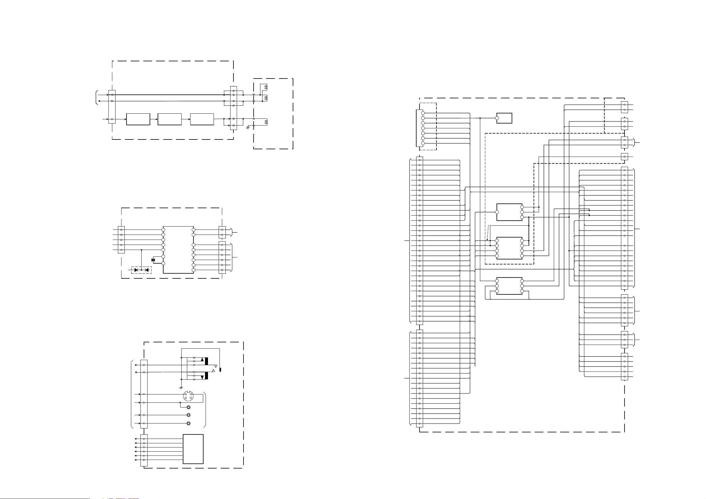
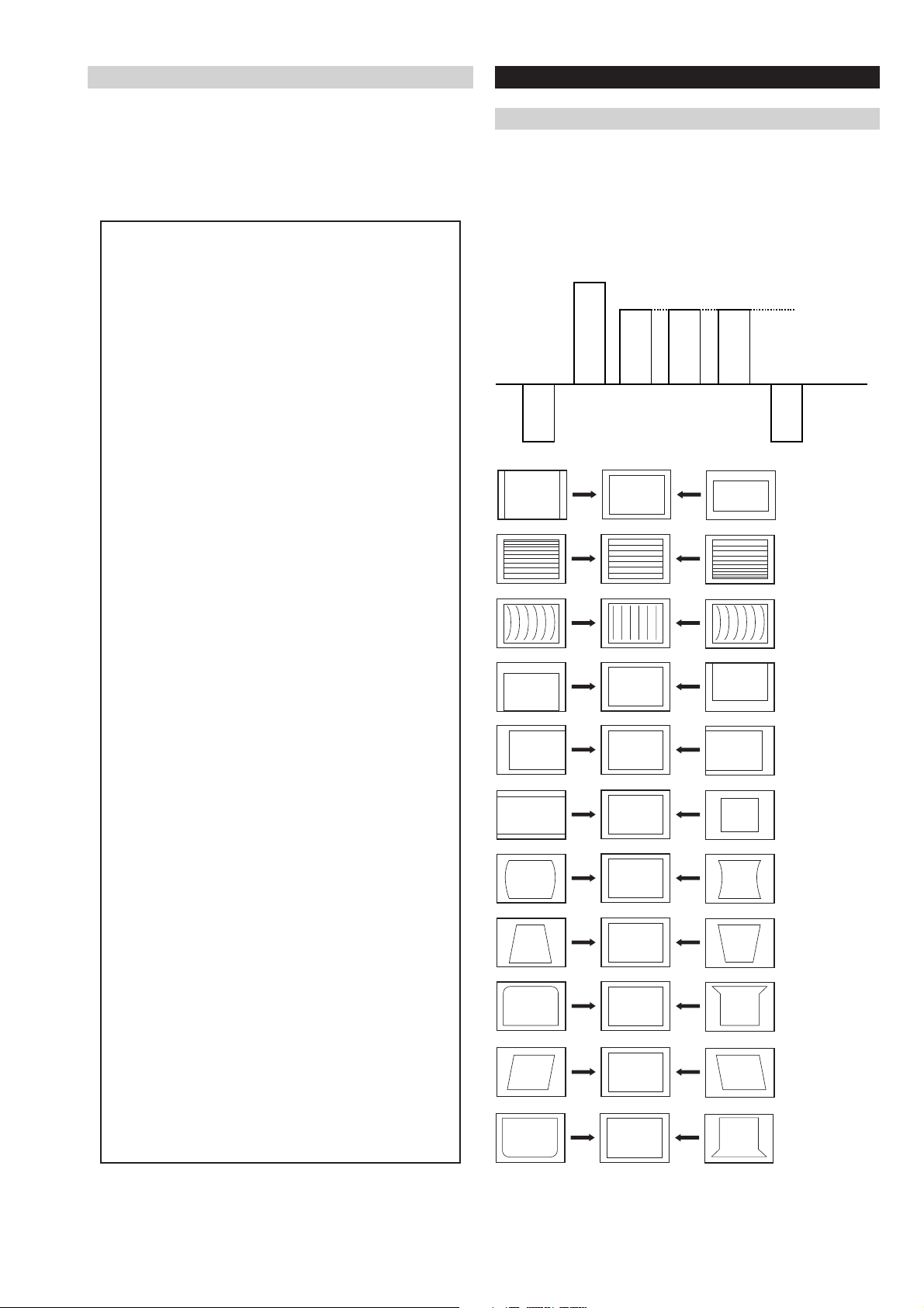
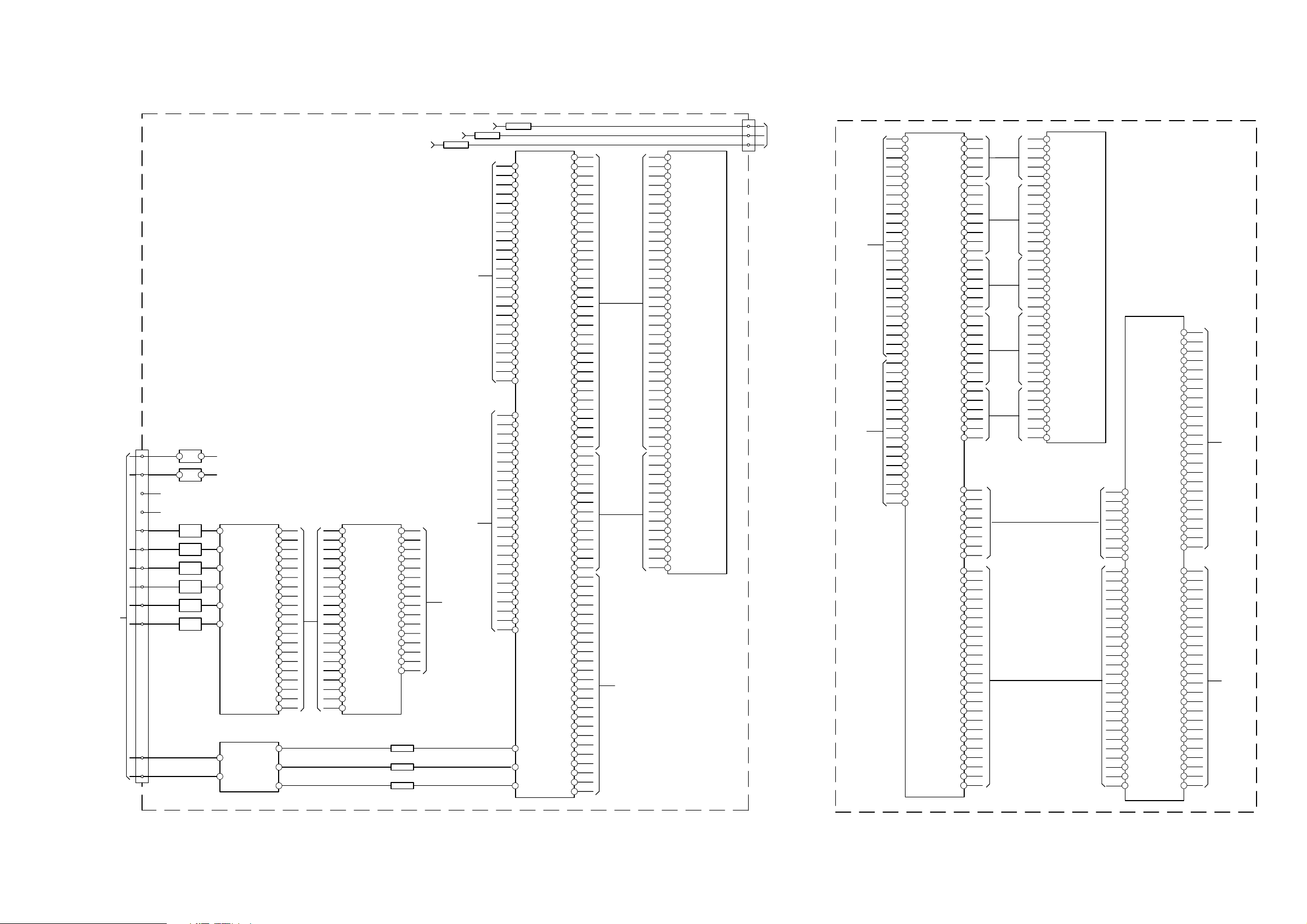
5-1. BLOCK DIA GRAMS (1)
TO
A BOARD
CN1803
VM ( )
VELOCITY MODULATION
CN5602
4
Q.P -
5
Q.P +
VM IN
1
CN302 IC300
VM AMP
Q5400,5401
AV LINK PROCESSOR
H ( )
1
SCL_3.3
SDA_3.3
3
AV_INT
5
RESET
6
AV-LINK
7
X300
3.3V
D302
CN907
1
3
TO A BOARD
CN1701
5
7
9
11
VM BUFFER
Q5402,5403,
5404,5405
23
SCL
24
SDA
22
INT
6
RESET
21 14
AV-LINK
28
OSC_OUT
29
OSC_IN
HEADPHONE R OUT
HEADPHONE L OUT
AV4 CHROMA IN
AV3 LUMINANCE IN
AV4 LEFT IN
AV4 RIGHT IN
SIRCS
RESP LED
VOL+
VOL-
RESET
BUTTON
AV-IN
PROG+
PROG-
4 3
2 1
Q5406,5407
20
17
15
11
10
9
8
Y/C
VIDEO
L
R
VM OUT
SIRCS
RESET -BUTTON
PROG+
PROG-
CN900
VOL+
VOL-
AV-IN
Q.P -
Q.P +
1
2
3
4
7
8
CN301
3
4RESP LED
CN300
1
2
3
4
5
6
J900
HEADPHONE
CN5444
TO
F4 BOARD
CN2161
TO
TOP CONTROLLER
QP-
QP+
VM
NECK
ASSY
TO
J2 BOARD
TO
B5 BOARD
CN4472
TU1001
CN1001
CN7109
ANALOGUE
TUNER
3
FBLK
5
V-PULSE
6
H-PULSE
7
MAIN-Y
9
MAIN-U
10
MAIN-V
11
CV-TEXT
13
SUB-C
14
SUB-Y
17
AV4.C
18
ATV-CV OUT
19
AV4.Y
21
AV-LINK
23
SDA
24
SCL
25
SDA1
26
SCL1
31
HP-MUTE
33
HP-R
34
HP-L
35
AV4-R
36
AV4-L
39
DTV-R
40
DTV-L
41
TV-R
42
TV-L
43
ATV-R
44
ATV-L
45
MAIN-R
46
MAIN-L
48
AGC MON
49
QSS
50
AM
1
MS-SHUT-DOWN
11
VP100 IN
12
HP100 IN
14
Y100
16
U100
18
V100
20
DPIC
22
RESET 100
23
SCL
24
SDA
31
VPSUBOUT/Y-SUB
34
VSUBOUT/C-SUB
36
USUBOUT/INT-COL
38
YSUBOUT/FB
42
MAIN-Y
44
MAIN-U
46
MAIN-V
48
V-PULSE
50
H-PULSE
AGC
SCL
SDA
FM/AM
QSS
VIDEO
VIDEO
AGC
AGC
VSYNC100
HSYNC100
SUB-Y
SUB-C
INT-COL
FBLK
TO
SHEET
CN2000
OCP
12
OVP
MAIN RY
DGCRY
LEFT SP
RIGHT SP
DISABLE
HM(1)
HM(2)
INT-COL
HM(3)
AV-LINK
HM(4)
SCL0
SDA0
VIDEO
TXTBLKBLK-MB
TXTB
STBY
TXTG
TXTR
SCL-DIG
SDA-DIG
VP100
HP100
SDA
DISABLE
HM(1)
HM(2)
HM(4)
HM(3)
AV LINK
13
CN1602
1
2
CN1201
1
TO SPEAKERS
3
CN1202
1
TO SUB WOOFER
CN1000
1
4
5
6
7
8
9
10
11
13
15
17
19
21
23
24
25
27
29
31
33
35
39
CN1701
1
3
5
7
9
11
CN1999
SCL
2
3
4
CN1706
1
3
5
6
7
TO
M2 BOARD
CN100
TO
H3 BOARD
CN907
TO
SERVICE
CP1100
1
SWATT
AUDIO
IC1201
AUDIO AMPLIFIER
WOOFER
1
WOOFER
AC-RY-LATCH
RIGHT
LEFT
OVP
2
OUTPUT
9 3
INPUT
BOOT
10
STBY/MUTE
IC1202
AUDIO AMPLIFIER
LEFT AND RIGHT
11
MUTE
6
MUTE
13
IN S+
8
IN C+
I/O EXPANDER
6
ATTN
1
0V PROT
4
DG CRY
A 1/2 ( )
IC1008
INTERFACE
STBY
STBY
OUT S
OUT C
PROT
14
9
1
3
15
SCL
14
SDA
OCP
10
AUDIO DECODER AND AMPLIFIER, VERTICAL DEFLECTION,
PICTURE ROTATION, DYNAMIC CONVERGENCE
SCL-TV
SDA-TV
CV TEXT
B-MB
G-MB
R-MB
SCL1
SDA1
VSYNC
HSYNC
HP-R
HP-L
AV4.C
AV4-Y AV3 LUMINANCE IN
AV4-L AV4 LEFT IN
AV4-R AV4 RIGHT IN
WOOFER SP
MS-SHUT-DOWN
SCL
SDA
AUDIO RESET
RESET 100
AUDIO MUTE
HEADPHONE RIGHT OUT
HEADPHONE LEFT OUT
AV4 CHRONA IN
VOL-
1
2
VOL+
3
PRESET
VIDEO
4
5
PROG -
6
PROG +
S900
S901
S902
S903
S904
S905
H3
FRONT AV INPUT,
HEADPHONE
(
)
- 31 -
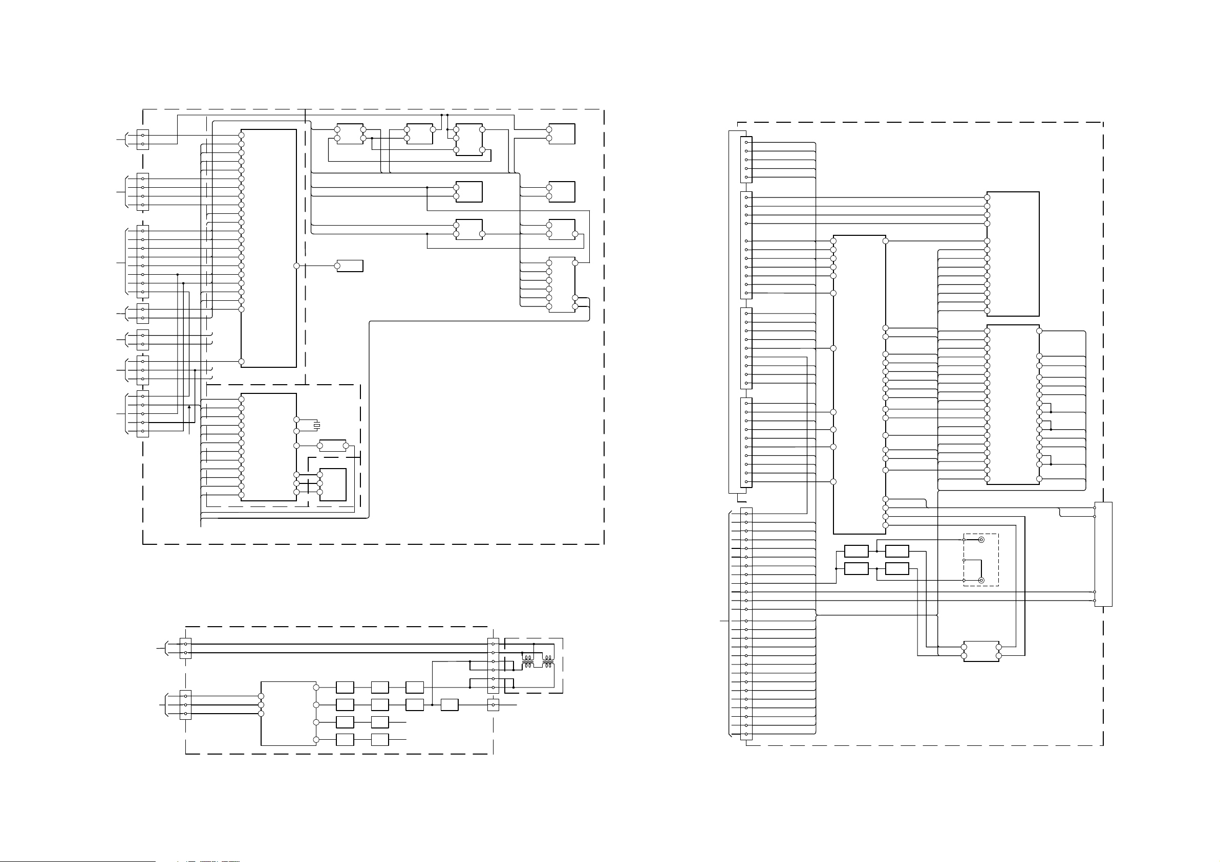
5-1. BLOCK DIA GRAMS (2)
J2 ( )
AV4
5
3
TO
A BOARD
3
11
25
26
31
33
34
46
45
19
36
10
9
7
42
41
14
18
CN3600
AV4-C-IN
TU3800
SUB TUNER
AV3L
AVFC
CVBS-TV-SUB
5
3
5
3
3
5
6
13
24
23
17
35
21
AV1
AV3
AV2
F-BLK-OUT
32
36
25
29
18
60
20
35
5
62
30
24
23
11
13
45
9
41
40
49
54
34
26
33
27
55
43
28
19
58
SWITCH
Q2302
SWITCH
Q2303
SWITCH
Q2300
SWITCH
Q2301
1
3
R OUT6L-IN
7
L OUT R-IN
HP-R-OUT
RGBSEL
5
2
15
4
3
6
7
8
14
13
12
11
10
IC3500
IC3400
48
16
18
47
45
17
46
44
5
32
22
2
20
19
13
14
7
9
4
42
40
39
37
33
29
23
3
1
26
25
6
12
11
CVBS-to-2149
J2300
L
R
STU-LR
SCL-DIG
SDA-DIG
VIDEO
FM/AM
SCL
SDA
HP-L-OUT
IC2300
HP OUT
V-IN-1-B
V-IN-1-G
V-IN-1-R
BLK-1
SEL
V-IN-2-B
V-IN-2-G
V-IN-2-R
BLK-2
BLK-OUT
V-OUT-B
V-OUT-G
V-OUT-R
BLUE IN
GREEN IN
RED IN
BLANKING
AV3ROUT
AV3LOUT
AV3C
AV3Y
AV3VOUT
AV4R
AV4L
AV4C
AVFL
AV3OUT
AVFY
AV4R-IN
L-to-1855
R-to-1855
AV4Y
AV3R
AV3MODE R-FRONT
R-SEL-OUTPUT
L-SEL-OUTPUT
C-AV
Y-AV3
CVBS-SEL-(AV3)
R-AV4
L-AV4
C-AV4
R-to-2149
L-to-2149-P26
L-FRONT
R-to-2149-P33
C-SUB
SCL
SDA
CVBS-from-2149
Y-FRONT
L-from-2149
R-from-2149
C-to-2149
Y-to-2149
L-to-2149
CVBS-to-2149
Y-AV4
CVBS-AV4
R-AV3
L-AV3
AV4MODE-1
AV4MODE-2
C-FRONT
LDO
CVBS-TV-SUB
IC3300
MAIN AUDIO/VIDEO SWITCH
STU-LR
Y-MAIN
C-MAIN
CVBS-TEXT
CVBS-SUB
L-TO-2149
SUB-TUNER
L-AV1
R-HP-VAR-OUTPUT
MAIN-TV
R-AV1
L-MAIN-TV
MODE 1
SUB-TV-(MOND)
CVBS-AV1
L-HP-VAR-OUTPUT
Y-MAIN-OUTPUT
C-MAIN-OUTPUT
MODE 3
Y-OUTPUT-TEXT
CVBS-SUB-OUTPUT
L-to-1855
R-to-1855
C-to-2149
Y-to-2149
R-from-1855-P32
L-from-1855-P22
R-from-1855-P20
L-from-1855-P33
CVBS-from-1855
CVBS-to-1855
R-AV2
L-AV2
MODE 2
Y-AV2
RIGHT IN(4) AV4R
LEFT IN(4) AV4L
MODE(4) AV4MODE
C IN(2) AV4C
Y IN AV4Y
BLUE IN
GREEN IN
RED IN
BLANKING
RIGHT OUT(1)
RIGHT IN(1)
LEFT OUT(1)
LEFT IN(1)
MODE(1)
VIDEO OUT(1)
VIDEO IN(1)
RIGHT OUT(3)
RIGHT IN(3)
LEFT OUT(3)
LEFT IN(3)
MODE(3)
AV LINK
C IN(1)
VIDEO OUT
VIDEO IN(3)
RIGHT OUT(2) RMONIT-OUT
RIGHT IN(2)
LEFT OUT(2) LMONIT-O UT
LEFT IN(2)
BLUE IN
MODE(2)
GREEN IN
RED IN
BLANKING
VIDEO(2) AV2V
AV-LINK
MAIN-R-OUT
MAIN-L-OUT
AV4R-IN
HP-L-OUT
HP-R-OUT
ATV-CV-IN/GNG
SUB-Y CVBS-SUB
HP-MUTE
SCL-DIG
SDA-DIG
CVBS-TEXT
B-OUT
G-OUT
R-OUT
MAIN-TV-R-IN
MAIN-TV-L-IN
AV4-L-IN
AV4-Y-IN
SDA
SCL
SUB-C
MAIN-C-OUT
MAIN-Y-OUT
CN1001
RMONIT-OUT
LMONIT-OUT
AV1TVOUT
AVFL
AVFY
AVFC
C-MAIN
Y-MAIN
AV3Y
AV3YOUT
AV3ROUT
AV3L
AV3LOUT
AV3R
AV1TVOUT
MAIN-TV-L-IN
MAIN-TV-R-IN
AV SCART, I/O
SWITCHING AND SOCKETS
TO
VM BOARD
CN5602
TO
C BOARD
CN5400
TO
D1 BOARD
CN8500
TO ROT COIL
TO CY
TO
D1 BOARD
CN8616
TO
D2 BOARD
CN6801
CN1803
1
VM
4
QP-
CN1804
1
R-OUT
3
G-OUT
5
B-OUT
8
IK
CN1805
1
DF-PARA
2
MP-PARA
3
E/W
4
HC-PARA
5
H-DRIVE
6
AFC-PULSE
7
ABL
8
XRAY
CN1901
1
ROT-
3
ROT+
CN1902
1
CY+
3
CY-
CN1807
1
PRE-RGB
2
DF-DRIVE
3
H-CENTRE
CN1903
4
H-PROT
5
HDP-OVP
6
AFC-PULSE
7
DF-DRIVE
8
ABL
TO
A BOARD
CN1802
T0
A BOARD
CN1805
AC-RY-LATCH
CN8612
CN8500
2
3
5
TO
SHEET 1
MP-PARA
EW
H-DRIVE
14
VM-OUT
DPIC
12
DPDT-OFF
Y100
20
Y-IN
U100
21
CB-IN
V100
22
CR-IN
64
R-OUT
63
G-OUT
62
B-OUT
58
42
28
46
45
47
43
40
39
56
25
26
51
60
IK-IN
VS-IN
HS-IN
DF-PARA
MP-PARA
EW-DRV
HC-PARA
H-DRV
HP-IN
APL-IN
SDA
SCL
VSAW1
PRE-RGB
VSYNC100
HSYNC100
BACK END BLOCK RESPONSIBILITY
2
SCL
3
TV-R
TV-L
ATV-R
ATV-L
DTV-L
DTV-R
MAIN-L
MAIN-R
AM
SDA
POWER ON
21
RESET
33
SC2-OUT-R
34
SC2-OUT-L
36
SC1-OUT-R
37
SC1-OUT-L
53
SC2-IN-L
54
SC2-IN-R
56
SC1-IN-L
57
SC1-IN-R
60
MONO IN (AM)
AUDIO RESET
IC1402
VPROT
DF-DRIVE
35
XTAL OUT
XTAL IN
IF IN
72
71
69
30 3
28
27
AUDIO
FL1270
4 1
IC1270
OUTPUT AMP
5
7
IC1231
SUBWOOFER OUT
SPEAKER OUT L
SPEAKER OUT R
IC8801
29
18
8
1
HD1 OUT
MP.PARA
EW
HD1N
HD2 OUT
LIN OUT
MP OUT
28
14
16
IC1801
7 5
3 6
VERTICAL
IC1701
1
QSS
BUFFER
Q8010
Q8011
BUFFER
Q8014
Q8015
BUFFER
Q8507
Q8508
BUFFER
Q8503
Q8504
DFPHASE
DQP-
AC-AMP
IC1804
2 1
3
AFC-PULSE
HC-PARA
DF-PARA
ABL
IC1808
7 5
1
DQP-PHASE
26
IC1811
7
4
IC1806
14
6
5 2
DQP-DC-LEVEL
ROTROT+
CY+
CY-
H-CENTRE
DQP-AC-AMP
DQP-DC-LEV
DF-PHASE
DQP-PHASE
MP-PARA
AUDIO DECODER AND AMPLIFIER, VERTICAL DEFLECTION,
A 2/2 ( )
PICTURE ROTATION, DYNAMIC CONVERGENCE
DY
ASSY
6
V+
5
V-
4
H-
3
HDT
T8100
HDT
T8101
LINEARITY
Q8106
INNER
PIN
Q8105
UPPER
H OUT
Q8102
LOWER
H OUT
Q8103
+B
+B
D1 ( )
T8202
HDT
HORIZONTAL
DEFLECTION
2
H+
1
TO
CN8614
5HEATER
C BOARD
CN5634
IC1811
4
1
IC1950
ROTATION (N/S)
2
4
IC1809
6
3
IC1803
10
8
12
3
7
9
4
21
20
H-LINEAR
SDA
SCL
- 32 -
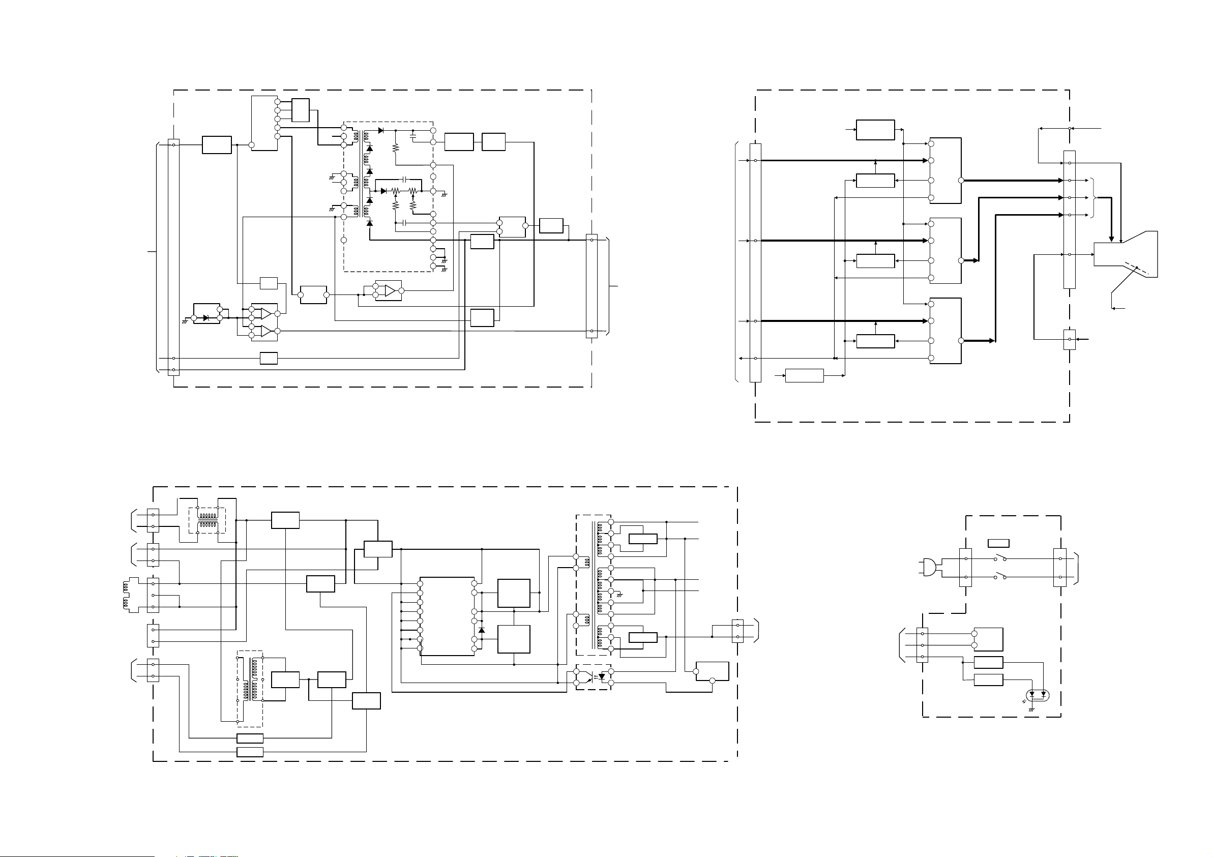
5-1. BLOCK DIA GRAMS (3)
2
4
SWITCH
Q2161
STBY 5V
TO H BOARD
CN301
CN2161
RESP LED
SWITCH
Q2160
OUT
IC2160
GR
1
5
POWER
S2650
CN2652CN2650
2
1
F4( )
POWER SWITCH, SIRCS
RECEIVER AND STAND-
BY LED INDICATOR
TO
G BOARD
CN6001
D2172
VCC
3
SIRCS
AC IN
AC IN
AC OUT
AC OUT
CN6801
1/2
6
TO
A BOARD
CN1903
7
8
AFC
PULSE
2 3
DF DRIVE
ABL
AFC PULSE
DETECT
Q6802, Q6803
IC6807
12
VG(L)
VG(H)
1
V SENSE
IC6800
BUFFER
Q6803
1
3
2
5
6
IC6801
Q8909
Q6804,
15
VS
Q6805
16
9
2
F/B
CATHODE
IC6803
1
7
9
8
200V
7
5
10
200V
6
4
3
11
43
REF
T6800
POWER ON SWITCH
HV
HV
OVERSHOOT
17
PROJECT
Q6816, Q6817
13
15
14
G2
16
FV
1
18
19
12
IC6802
7
5
6
SS RESET
Q6814,
Q6813
6
DYNAMIC
3
FOCUS
T8901
1
ABL
PROTECT
Q6807
UNDER
VOLTAGE
PROTECT
Q6808
D2 ( )
DYNAMIC
FOCUS
Q8918
HPROT
HOP OV
DYNAMIC PICTURE
STABILISING CIRCUIT
CN6801
2/2
4
5
TO
A BOARD
CN1903
TO A BOARD
CN1804
CN5400
R
1
G
3
B
5
IK
8
VOLTAGE DET
+12V
Q5375, 5376
+12V
Q5350
STANBY SW
Q5300
STANBY SW
Q5325
STANBY SW
Q5351
IC5300
VIDEO OUT (RED)
1
VB
3
VI
9
VDF
VO
5
IK
IC5325
VIDEO OUT (GREEN)
1
VB
3
VI
9
VDF
VO
5
IK
IC5350
VIDEO OUT (BLUE)
1
VB
3
VI
9
VDF
VO
5
IK
8
8
8
FV
G4
R
10
G
9
B
8
H1
5
H1
5
J5375
CN5634
TO D2 BOARD
FV (T6800)
PICTURE TUBE
HV
TO D1 BOARD
CN8614
TO D2 BOARD
HV (T6800)
TO F4 BOARD
CN2652
FOR CHECK
TO A BOARD
CN1602
CN6001
CN6002
CN6003
CN6004
CN6008
R, G, B OUT
C (
)
T6003
4
AC IN
1
5
AC IN
CHECK
1
2
CHECK
1
DGC
DGC
2
3
DGC
1
PFC
3
PFC
MAIN RY
1
2
DGC RY
3
2
1
T6101
1
2
3
4
RELAY
RY6001
MAIN RECT
D6001
RELAY
RY6002
7
8
RECT
D6102
9
RELAY
SWITCH
Q6103
RELAY
SWITCH
Q6101
MAIN BRIDGE
1
V SENSE
2
F/B
3
CT
4RT
TIMER
6
7
SS
8
VC 1
9
OCP
IC6001
RECTIFIER
VG (L)
18
VD
16
VG
15
VS
14
VB
12
VC 2
10
D6004
MOSFET
TRANSISTOR
USED BY
SWITCHING
CIRCUIT Q6006
MOSFET
TRANSISTOR
USED BY
SWITCHING
CIRCUIT Q6007
T6002
10
11
RECT
D6010
12
6
8
7
9
13
14
15
16
17
18
1
RECT
2
D6016
3
PH6001
4
3
1
2
+200V
+135V
+11V
+6V
CN6006
AU (+)
5
TO A BOARD
AU (+)
6
CN2000
IC6003
1
2
Q6104
Q6105
G ( )
- 33 -
POWER
SUPPLY
DB09
DQ3
DQ2
DQ1
DQ0
ADDR11
DQ7
DQ6
DQ5
DQ4
XCAS
XRAS
153
152
154
150
151
139
138
136
137
135
133
129
134
128
149
148
140
147
126
125
127
124
123
192
193
195
196
194
199
201
202
200
203
122
189
191
190
DQ11
DQ10
DQ9
DQ8
ADDR9
ADDR0
DQ15
DQ14
DQ13
DQ12
ADDR2
ADDR1
204
205
206
10
11
9
14
13
19
20
36
35
46
48
49
47
25
15
16
18
17
27
28
26
29
30
39
40
42
41
31
32
38
37
7
8
TO
SHEET 1/2 (B)
TO
SHEET 1/2 (A)
DB08
DB07
DB06
DB05
DB04
DB03
DB02
DR09
DR08
DR07
DR06
DR05
DR04
DR03
DR02
DY09
DY08
DY07
DY06
DY05
DY04
DY03
DY02
DIC00
DIC01
DIC02
DIC03
DIC04
DIC05
DIC06
DIC07
DIY00
DIY01
DIY02
DIY03
DIY04
DIY05
DIY06
DIY07
XWE
DOM
XCS
ADDR10
ADDR3
ADDR8
ADDR7
ADDR6
ADDR5
ADDR4
17
15
16
18
14
6
5
2
3
19
21
22
20
23
12
11
8
9
49
48
24
46
45
32
31
29
28
30
27
43
42
39
40
DQ(3)
DQ(2)
DQ(1)
DQ(0)
ADDR(11)
DQ(7)
DQ(6)
DQ(5)
DQ(4)
XCAS
XRAS
DQ11
DQ10
DQ9
DQ8
ADDR9
ADDR(0)
DQ15
DQ14
DQ13
DQ12
ADDR(2)
ADDR(1)
XWE
DOM
XCS
ADDR(10)
ADDR(3)
ADDR8
ADDR7
ADDR6
ADDR5
ADDR4
DQ(3)
DQ(2)
DQ(1)
DQ(0)
ADDR(11)
DQ(7)
DQ(6)
DQ(5)
DQ(4)
XCAS
XRAS
DQ11
DQ10
DQ9
DQ8
ADDR9
ADDR(0)
DQ15
DQ14
DQ13
DQ12
ADDR(2)
ADDR(1)
XWE
DOM
XCS
ADDR(10)
ADDR(3)
ADDR8
ADDR7
ADDR6
ADDR5
ADDR4
DQ3
DQ2
DQ1
DQ0
ADDR11
DQ7
DQ6
DQ5
DQ4
CAS
RAS
DQ11
DQ10
DQ9
DQ8
ADDR9
ADDR0
DQ15
DQ14
DQ13
DQ12
ADDR2
ADDR1
WE
LDGM
CS
ADDR10
ADDR3
ADDR8
ADDR7
ADDR6
ADDR5
ADDR4
IC4203
IC4201
B5 (2/2)
( )
PICTURE DECODER, DRC,
DIGITAL NOISE REDUCTION
IOPORT7
IOPORT6
7
8
6
11
11
132
131
129
130
128
124
123
125
122
12
135
133
134
120
119
121
118
116
111
110
109
115
114
112
113
4
5
TO
SHEET 1/2 (C)
DRCCBIN0
IP7
IC4304
IOPORT5
IOPORT4
IOPORT3
IOPORT2
IOPORT1
IOPORT0
IP6
IP5
IP4
IP3
IP2
IP1
IP0
57
58
59
69
80
93
81
60
IP7
IP6
IP5
IP4
IP3
IP2
IP1
IP0
FV
FH
PXI
FFSW
GAME
SO
S1
VSTILL1
DB03
DB04
DB05
DB06
DB07
DB02
150
151
153
152
154
134
135
133
136
147
149
148
138
139
137
140
122
127
128
129
123
124
126
125
DB08
DB09
DSB(3)
DSB(4)
DSB(5)
DSB(6)
DSB(7)
DSB(2)
DSR(4)
DSR(2)
DSR(3)
DSB(8)
DSB(9)
DR03
DR04
DR05
DR06
DR07
DR02
DR08
DR09
DY03
DY04
DY05
DY06
DY07
DY02
DY08
DY09
DSR(5)
DSR(6)
DSR(7)
DSR(8)
DSR(9)
DSY(4)
DSY(2)
DSY(3)
DSY(5)
DSY(6)
DSY(7)
DSY(8)
DSY(9)
DSB(3)
DSB(4)
DSB(5)
DSB(6)
DSB(7)
DSB(2)
DSR(4)
DSR(2)
DSR(3)
DSB(8)
DSB(9)
DSR(5)
DSR(6)
DSR(7)
DSR(8)
DSR(9)
DSY(4)
DSY(2)
DSY(3)
DSY(5)
DSY(6)
DSY(7)
DSY(8)
DSY(9)
DRCCBIN1
DRCCBIN2
DRCCBIN3
DRCCBIN4
DRCCBIN5
DRCCBIN6
DRCCBIN7
DRCCRIN0
DRCCRIN1
DRCCRIN2
DRCCRIN3
DRCCRIN4
DRCCRIN5
DRCCRIN6
DRCCRIN7
DRCCYIN0
DRCCYIN1
DRCCYIN2
DRCCYIN3
DRCCYIN4
DRCCYIN5
DRCCYIN6
DRCCYIN7
48
49
51
50
52
56
57
53
58
44
47
46
60
61
59
62
63
69
70
71
64
65
68
67
DSPCRIN0
DSPCRIN1
DSPCRIN2
DSPCRIN3
DSPCRIN4
DSPCRIN5
DSPCRIN6
DSPCRIN7
DSPCBIN0
DSPCBIN1
DSPCBIN2
DSPCBIN3
DSPCBIN4
DSPCBIN5
DSPCBIN6
DSPCBIN7
DSPCYIN0
DSPCYIN1
DSPCYIN2
DSPCYIN3
DSPCYIN4
DSPCYIN5
DSPCYIN6
DSPCYIN7
RP(1)
RP(2)
RP(3)
RP(4)
RP(5)
RP(0)
BP(2)
BP(0)
RP(6)
RP(7)
BP(3)
BP(4)
BP(5)
BP(6)
BP(7)
GP(2)
GP(0)
GP(3)
GP(4)
GP(5)
GP(6)
GP(7)
BP(1)
GP(1)
TO
SHEET 1/2 (D)
99
98
96
97
95
93
92
94
89
104
100
103
87
86
88
85
82
76
75
74
80
79
77
78
DY(5)
DY(7)
DY(4)
DY(3)
DY(2)
DY(1)
DY(0)
DY(6)
DRCCYOUT0
DRCCYOUT1
DRCCYOUT2
DRCCYOUT3
DRCCYOUT4
DRCCYOUT5
DRCCYOUT6
DRCCYOUT7
DRCCROUT0
DR(5)
DR(7)
DR(4)
DR(3)
DR(2)
DR(1)
DR(0)
DR(6)
DRCCROUT1
DRCCROUT2
DRCCROUT3
DRCCROUT4
DRCCROUT5
DRCCROUT6
DRCCROUT7
DB(5)
DB(7)
DB(4)
DB(3)
DB(2)
DB(1)
DB(0)
DB(6)
DRCCBOUT1
DRCCBOUT2
DRCCBOUT3
DRCCBOUT4
DRCCBOUT5
DRCCBOUT6
DRCCBOUT7
DRCCBOUT0
5-1. BLOCK DIAGRAMS (4)
A BOARD
CN7109
CN4472(1/2)
TO
11
12
23
24
38
42
44
46
48
50
31
34
VP100 OUT
HP100 OUT
SCL
SDA
FBIN
BIN
GIN
RIN
CV/Y MAIN IN
C MAIN IN
SUB CVBS
C SUB IN
IC4403
VP-100
442
OUT
HP-100
OUT
IC4402
BUFFER
Q3119
BUFFER
Q3116
BUFFER
Q3110
BUFFER
Q3120
BUFFER
Q3108
BUFFER
Q3106
2
CN4472(2/2)
14
IC4602
Y 100 OUT
U 100 OUT
V 100 OUT
16
18
AMP Q4903
PDACY
AMP Q4904
PDACU
AMP Q4905
PDACV
RP(0)
71
DSPCR0
RP(1)
70
DSPCR1
RP(2)
69
DSPCR2
RP(3)
68
DSPCR3
RP(4)
65
DSPCR4
RP(5)
64
DSPCR5
RP(6)
63
DSPCR6
RP(7)
62
DSPCR7
35
AIN6
29
AIN4
24
AIN3
32
AIN5
16
AIN2
12
AIN1
IC4602
IC3100
CLKO
COUT2
COUT3
COUT4
COUT5
COUT6
COUT7
COUT8
COUT9
YOUT2
YOUT3
YOUT4
YOUT5
YOUT6
YOUT7
YOUT8
YOUT9
LIEN
VSO
HSO
154
153
152
151
144
143
142
137
136
135
134
133
126
125
124
119
118
117
116
115
CGEN
CLKO
VSO
HSO
DCOBC(0)
DCOBC(1)
DCOBC(2)
DCOBC(3)
DCOBC(4)
DCOBC(5)
DCOBC(6)
DCOBC(7)
DCOBY(0)
DCOBY(1)
DCOBY(2)
DCOBY(3)
DCOBY(4)
DCOBY(5)
DCOBY(6)
DCOBY(7)
23
CrOUT
IC3200
CbOUT
YOUT
22
21
48
1
CVBS/Y1
C1
TO SHEET 2 (C)
51
CGEN
52
CLKINB
53
VDINB
54
HDINB
26
CINB0
27
CINB1
30
CINB2
31
CINB3
32
CINB4
33
CINB5
34
CINB6
35
CINB7
38
YINB0
39
YINB1
40
YINB2
41
YINB3
42
YINB4
43
YINB5
IC4602
44
YINB6
45
YINB7
IC4401
COUT0
COUT1
COUT2
COUT3
COUT4
COUT5
COUT6
COUT7
YOUT0
YOUT1
YOUT2
YOUT3
YOUT4
YOUT5
YOUT6
YOUT7
DICO(0)
96
DICO(1)
95
DICO(2)
94
DICO(3)
93
DICO(4)
92
DICO(5)
91
DICO(6)
90
DICO(7)
89
DIYO(0)
85
DIYO(1)
84
DIYO(2)
83
DIYO(3)
82
DIYO(4)
79
DIYO(5)
78
DIYO(6)
77
DIYO(7)
76
AMP Q3206
AMP 3205
AMP 3204
TO
SHEET 1/2 (D)
TO SHEET 2 (B)
BP(0)
BP(1)
BP(2)
BP(3)
BP(4)
BP(5)
BP(6)
BP(7)
GP(0)
GP(1)
GP(2)
GP(3)
GP(4)
GP(5)
GP(6)
GP(7)
CB(7)
CB(6)
CB(5)
CB(4)
CB(3)
CB(2)
CB(1)
CB(0)
CR(7)
CR(6)
CR(5)
CR(4)
CR(3)
CR(2)
CR(1)
CR(0)
Y(7)
Y(6)
Y(5)
Y(4)
Y(3)
Y(2)
Y(1)
Y(0)
61
60
59
58
57
56
53
52
51
50
49
48
47
46
45
44
11
12
13
14
15
16
17
20
21
22
23
24
26
27
28
29
31
32
33
34
35
39
40
41
208
210
215
DSPCB0
DSPCB1
DSPCB2
DSPCB3
DSPCB4
DSPCB5
DSPCB6
DSPCB7
DSPY0
DSPY1
DSPY2
DSPY3
DSPY4
DSPY5
DSPY6
DSPY7
DRCCBIN7
DRCCBIN6
DRCCBIN5
DRCCBIN4
DRCCBIN3
DRCCBIN2
DRCCBIN1
DRCCBIN0
DRCCRIN7
DRCCRIN6
DRCCRIN5
DRCCRIN4
DRCCRIN3
DRCCRIN2
DRCCRIN1
DRCCRIN0
DRCYIN7
DRCYIN6
DRCYIN5
DRCYIN4
DRCYIN3
DRCYIN2
DRCYIN1
DRCYIN0
ANCRIN
ANCBIN
ANYGIN
DRCCRIN0
DRCCRIN1
DRCCRIN2
DRCCRIN3
DRCCRIN4
DRCCRIN5
DRCCRIN6
DRCCRIN7
DRCCBIN0
DRCCBIN1
DRCCBIN2
DRCCBIN3
DRCCBIN4
DRCCBIN5
DRCCBIN6
DRCCBIN7
IC4600
SDDAT31
SDDAT30
SDDAT29
SDDAT28
SDDAT27
SDDAT26
SDDAT25
SDDAT24
SDDAT23
SDDAT22
SDDAT21
SDDAT20
SDDAT19
SDDAT18
SDDAT17
SDDAT16
SDDAT15
SDDAT14
SDDAT13
SDDAT12
SDDAT11
SDDAT10
SDDAT9
SDDAT8
SDDAT7
SDDAT6
SDDAT5
SDDAT4
SDDAT3
SDDAT2
SDDAT1
SDDAT0
SDADR0
SDADR1
SDADR2
SDADR3
SDADR4
SDADR5
SDADR6
SDADR7
SDADR8
SDADR9
SDADR10
SDADR11
SDADR12
DRCYIN0
DRCYIN1
DRCYIN2
DRCYIN3
DRCYIN4
DRCYIN5
DRCYIN6
DRCYIN7
D(31)
99
D(30)
100
D(29)
103
D(28)
104
D(27)
105
D(26)
106
D(25)
108
D(24)
109
D(23)
110
D(22)
111
D(21)
112
D(20)
113
D(19)
116
D(18)
117
D(17)
118
D(16)
119
D(15)
158
D(14)
159
D(13)
160
D(12)
161
D(11)
164
D(10)
165
D(9)
166
D(8)
167
D(7)
148
D(6)
149
D(5)
151
D(4)
152
D(3)
153
D(2)
154
D(1)
155
D(0)
157
A(0)
131
A(1)
130
A(2)
129
A(3)
120
A(4)
121
A(5)
122
A(6)
123
A(7)
124
A(8)
125
A(9)
128
A(10)
132
A(11)
133
A(12)
134
Y(0)
41
Y(1)
40
Y(2)
39
Y(3)
35
Y(4)
34
Y(5)
33
Y(6)
32
Y(7)
31
CR(0)
29
CR(1)
28
CR(2)
27
CR(3)
26
CR(4)
24
CR(5)
23
CR(6)
22
CR(7)
21
CB(0)
20
CB(1)
17
CB(2)
16
CB(3)
15
CB(4)
14
CB(5)
13
CB(6)
12
CB(7)
11
D(31)
55
DQ31
D(30)
54
DQ30
D(29)
53
DQ29
D(28)
51
DQ28
D(27)
50
DQ27
D(26)
48
DQ26
D(25)
47
DQ25
D(24)
45
DQ24
D(23)
42
DQ23
D(22)
40
DQ22
D(21)
39
DQ21
D(20)
37
DQ20
D(19)
36
DQ19
D(18)
34
DQ18
D(17)
33
DQ17
D(16)
31
DQ16
D(15)
85
DQ15
D(14)
83
DQ14
D(13)
82
DQ13
D(12)
80
DQ12
D(11)
79
DQ11
D(10)
77
DQ10
D(9)
76
DQ9
D(8)
75
DQ8
D(7)
13
DQ7
D(6)
11
DQ6
D(5)
10
DQ5
D(4)
8
DQ4
D(3)
7
DQ3
D(2)
5
DQ2
D(1)
4
DQ1
D(0)
3
DQ0
A(0)
25
A0
A(1)
26
A1
A(2)
27
A2
A(3)
60
A3
A(4)
61
A4
A(5)
62
A5
A(6)
63
A6
A(7)
64
A7
A(8)
65
A8
A(9)
66
A9
A(10)
24
A10
A(11)
23
A11
A(12)
22
A12
TO SHEET 2 (A)
B5 (1/2)
PICTURE DECODER, DRC,
DIGITAL NOISE REDUCTION
( )
- 34 -

5-1. BLOCK DIA GRAMS (5)
5-2. CIRCUIT BOARD LOCATION
5-3. SCHEMATIC DIAGRAMS AND
PRINTED WIRING BOARDS
Note :
• All capacitors are in µF unless otherwise noted.
• pF : µµF 50WV or less are not indicated except for
electrolytic types.
• Indication of resistance, which does not have one for
rating electrical power, is as follows.
Pitch : 5mm
Electrical power rating : 1/4W
• Chip resistors are 1/10W
• All resistors are in ohms.
k = 1000 ohms, M = 1000,000 ohms
• : nonflammable resistor.
• : fusible resistor.
• : internal component.
• : panel designation or adjustment for repair.
• All variable and adjustable resistors have
characteristic curve B, unless otherwise noted.
• All voltages are in Volts.
• Readings are taken with a 10Mohm digital mutimeter.
• Readings are taken with a color bar input signal.
• Voltage variations may be noted due to normal production
tolerences.
•: B + bus.
• : B - bus.
• : RF signal path.
• : earth - ground.
• : earth - chassis.
Reference Information
RESISTOR RN
: METAL FILM
RC
: SOLID
FPRD
: NON FLAMMABLE CARBON
FUSE
: NON FLAMMABLE FUSIBLE
RS
: NON FLAMMABLE METAL OXIDE
RB
: NON FLAMMABLE CEMENT
RW
: NON FLAMMABLE WIREWOUND
: ADJUSTMENT RESISTOR
COIL LF-8L
: MICRO INDUCTOR
CAPACITOR TA
: TANTALUM
PS
: STYROL
PP
: POLYPROPYLENE
PT
: MYLAR
MPS
: METALIZED POLYESTER
MPP
: METALIZED POLYPROPYLENE
ALB
: BIPOLAR
ALT
: HIGH TEMPERATURE
ALR
: HIGH RIPPLE
Les composants identifiés par une trame et
par une marque sont d'une importance
critique pour la sécurité. Ne les remplacer
que par des pièces de numéro spécifié.
specified.
Note :
The components identified by shading
and marked are critical for safety.
Replace only with the part numbers
specified in the parts list.
Note :
CVM Board
A Board
S1 Board
VM
C
H
D1
A
J
A2
N
D
A1
D2
C
A
VM Board
C Board
A Board
M2 Board
G Board
H Board
H3 Board
D2 Board
D1 Board
B5 Board
J2 Board
F4 Board
CN100/1
1
CS DISABLE
4
KEY2/SCL3.3
6
KEY1/SCL3.3
INT-COL
RESET
AVL-INT
CVBS IN (TXT)
RESET
TXT BLK
TXTB
PROT
AC-ON/OFF
VP100
HP100
P2(13)
OUT IC101
7
8
10
17
20
21
22
26
28
33
35
40
TO
BOARD A
CN1000
11
P2.14
100
P6.5
97
RESET AUDIO P3.7
P6.2
5
P2.8 INT. COL
12
P2.15 AVL INT
121
CVBSIA
105
BLANK/CORBLA
7
P2.10
8
P2.11 PROT
9
P2.12 AC ON/OFF
102
V SYNC
103
H SYNC
10
P2.13 VIPER WRITE
37
36
35
34
33
27
26
24
23
25
28
29
30
38
39
A14/RAS
40
A15/CAS
22
P4.3/A16
19
P4.1/A17
18
P4.2/A18
17
P4.3/A19
MICRO PROCESSOR
AND TEXT DECODER
IC103
AGC DEFEAT P3.2
AUDIO MUTE P3.5
124
P5.0
RESET 100 P3.6
114
B
STDBY P3.4
113
G
112
R
3.12
P6.3
P6.4
P3.11
P3.10
D0
D1
D2
D3
D4
D5
D6
D8
D9
D10
D11
D12
D13
D14
D15
UDQM
MEMCLK
CLKEN
/WE
LDQM
CSROM
RD
CS DISABLE
A(0)
A(1)
A(2)
A(3)
A(4)
A(5)
A(6)
A(7)
A(8)
A(9)
A(10)
A(11)
A(12)
A(13)
A(14)
A(15)
A(16)
A(17)
A(18)
A(19)
M2( )
AGC-MON
AGC-DEFEAT
76
81
80
78
79
90
98
99
RXDO
89
TXDO
88
D(0)
55
D(1)
59
D(2)
65
D(3)
71
D(4)
70
D(5)
64
D(6)
58
D(8)
57
D(9)
63
D(10)
67
D(11)
72
D(12)
66
D(13)
62
D(14)
56
D(15)
51
48
43
45
50
49
46
47
D(0)
D(1)
D(2)
D(3)
D(4)
D(5)
D(6)
D(8)
D(9)
D(10)
D(11)
D(12)
D(13)
D(14)
D(15)
D(7)
D(7)
MS SHUT DOWN
RESET AUDIO
RESET 100
7
WP
6
SCL1
5
SDA1
AUDIO-MUTE
IC104
2
IC105
DQ0
4
DQ1
5
DQ2
7
DQ3
8
DQ4
10
DQ5
11
DQ6
42
DQ8
44
DQ9
45
DQ10
47
DQ11
48
DQ12
50
DQ13
51
DQ14
53
DQ15
13
DQ7
39
DQM
38
CLK
37
CKE
IC107
31
Q7
15
Q0
17
Q1
19
Q2
21
Q3
25
Q4
27
CLKINB
Q5
29
Q6
16
Q8
18
Q9
20
Q10
22
Q11
26
Q12
28
Q13
30
Q14
32
Q15
23
NC
12
/E1
14
/G
BA0/A12
BA1/A13
/RAS
/CAS
LDQM
23
A0
24
A1
25
A2
26
A3
A4
29
30
A5
31
A6
A7
32
33
A8
34
A9
A10
22
35
A11
20
21
18
17
16
/WE
15
A(0)
11
A0
A(1)
10
A1
A(2)
9
A2
A(3)
8
A3
A(4)
7
A4
A(5)
6
A5
A(6)
A6
5
A(7)
4
A7
A(8)
43
A8
A(9)
42
A9
A(10)
41
A10
A(11)
40
A11
A(12)
39
A12
A(13)
38
A13
A(14)
37
A14
A(15)
36
A15
A(16)
35
A16
A(17)
3
A17
A(18)
2
A18
A(19)
44
A19
TXTB
ST.BY
TXTG
TXTR
RXDO
TXDO
BOOT
5
15
19
23
24
25
27
39
3
4
5
CN100/2
CN104
TO
BOARD A
CN1000
- 35 -
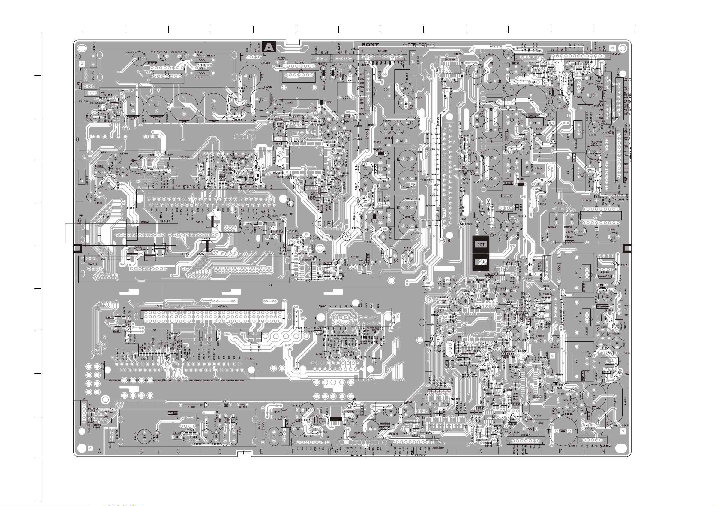
ABCDE F
1
2
3
4
G
HIJKLMN
5
6
7
8
9
10
11
~ A Printed Wiring Board Conductor side A ~
- 36 -
 Loading...