

Page 1
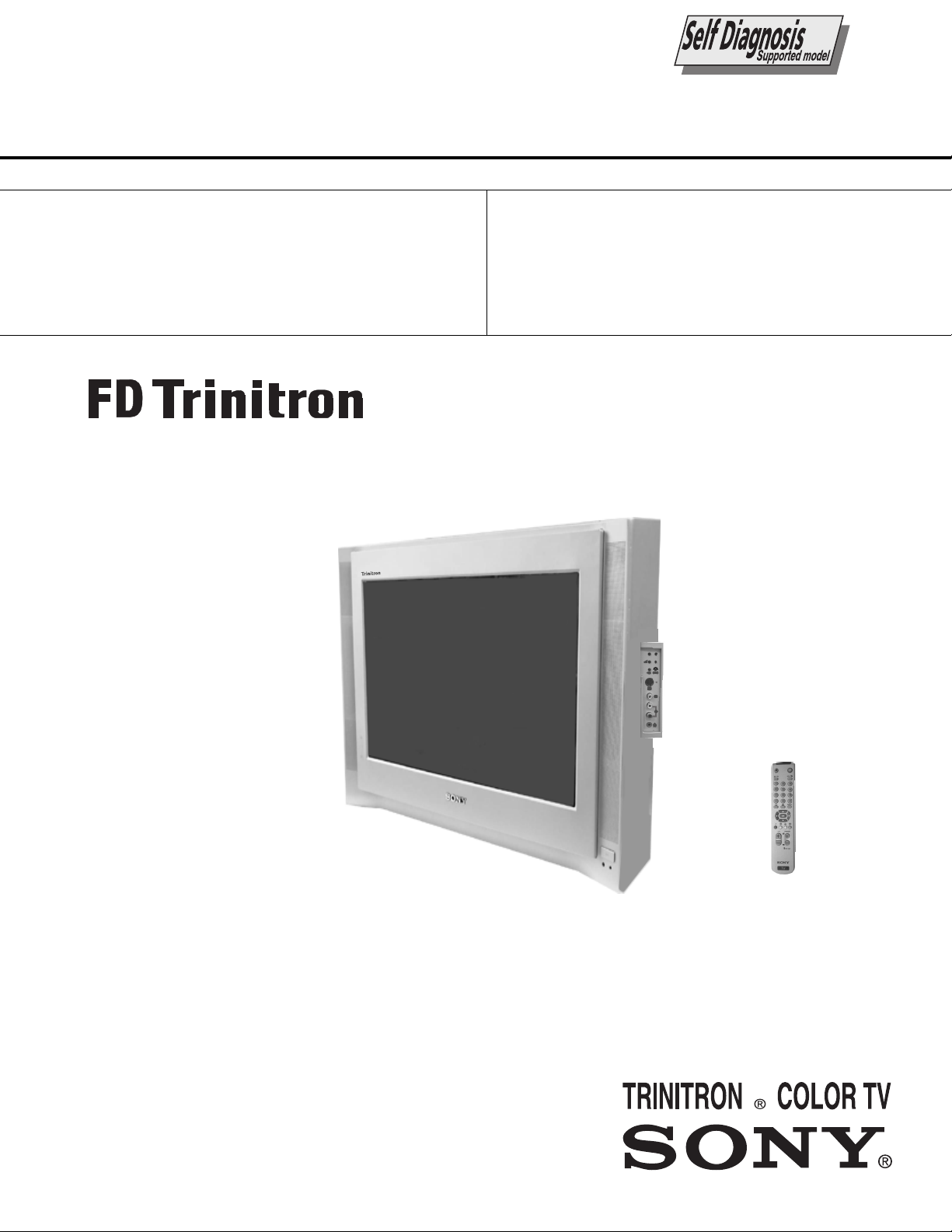
SERVICE MANUAL
AE-5
CHASSIS
MODEL
KV-29FX65B
KV-29FX65E
COMMANDER DEST CHASSIS NO.
RM-887 FRENCH SCC-Q13H-A
RM-887 ES P SCC-Q14H-A
MODEL
KV-29FX65K
COMMANDER DEST CHASSIS NO.
RM-887 OIRT SCC-Q16L-A
p
- +
s
4
4
MONO
L/G/S/I
4
R/D/D/D
1
Page 2

TABLE OF CONTENTS
Section Title Page Section Title Page
Specifications .................... 3
Connectors .................... 4
Self Diagnostic Software .................... 5
1. GENERAL
Tuning your TV .................... 8
Finding your V ideo Channel .................... 8
NexT V iew .................... 8
T eletext .................... 9
Using the TV menu system .................... 10
Specifications .................... 14
Troubleshooting .................... 14
2. DISASSEMBLY
2-1. Rear Cover Removal .................... 15
2-2. Speaker Connector .................... 15
2-3. Chassis Removal .................... 15
2-4. Service Position .................... 16
2-5. D1 Board Removal .................... 16
2-6. J Board Removal .................... 16
2-7. B2 Board Removal .................... 17
2-8. SideControl Removal .................... 17
2-9. F4 Bracket Removal .................... 17
2-10. F4 and H8 Board Removal .................... 17
2-11. Picture Tube Remov al .................... 18
Bottom Plates .................... 19
3. SET-UP ADJUSTMENTS
3-1. Beam Landing .................... 20
3-2. Convergence .................... 21
3-3. Focus, Screen [G2] Adjustment.................... 23
3-4. White Balance .................... 23
5. DIAGRAMS
5-1. Block Diagram (1) .................... 31
Block Diagram (2) .................... 35
Block Diagram (3) .................... 39
Block Diagram (4) .................... 43
5-2. Circuit Board Location .................... 46
5-3. Schematic Diagrams and
Printed Wiring Boards .................... 46
* H7 Board .................... 47
* H8 Board .................... 47
* F4Board .................... 48
* F1 Board .................... 48
* E Board .................... 49
* M1 Board .................... 53
* D1 Board .................... 56
* D Board .................... 63
* A Board .................... 66
* J Board .................... 75
* C Board .................... 81
* VM Board .................... 83
* B2 Board .................... 85
5-4. Semiconductors .................... 89
5-5. IC Blocks .................... 88
6. EXPLODED VIEWS
6-1. Chassis .................... 92
6-2. Picture Tube .................... 93
7. ELECTRICAL PARTS LIST .................... 94
4. CIRCUIT ADJUSTMENTS
4-1. Electrical Adjustments .................... 24
4-2. V olume Electrical Adjustments .................... 28
4-3. T est Mode 2 .................... 29
CAUTION
SHORT CIRCUIT THE ANODE OF THE PICTURE TUBE AND THE
ANODE CAP TO THE CARBON PAINTED ON THE CRT, AFTER
REMOVAL OF THE ANODE CAP.
WARNING !!
AN ISOLATION TRANSFORMER MUST BE USED DURING ANY
SERVICE WORK TO AVOID POSSIBLE SHOCK HAZARD DUE TO
LIVE CHASSIS, THE CHASSIS OF THIS RECEIVER IS DIRECTLY
CONNECTED TO THE POWER LINE.
SAFETY-RELATED COMPONENT WARNING !!
COMPONENTS IDENTIFIED BY SHADING AND MARKED
THE SCHEMATIC DIAGRAMS, EXPLODED VIEWS AND IN THE
PARTS LIST ARE CRITICAL FOR SAFE OPERATION. REPLACE
THESE COMPONENTS WITH SONY PARTS WHOSE PART
NUMBERS APPEAR AS SHOWN IN THIS MANUAL OR IN
SUPPLEMENTS PUBLISHED BY SONY.
£
ON
ATTENTION
APRES AVOIR DECONNECTE LE CAP DE’LANODE,
COURT-CIRCUITER L’ANODE DU TUBE CATHODIQUE ET CELUI
DE L’ANODE DU CAP AU COUCHE DE CARBONE PEINTE SUR
LE TUBE CATHODIQUE.
ATTENTION !!
AFIN D’EVITER TOUT RISQUE D’ELECTROCUTION PROVENANT
D’UN CHÁSSIS SOUS TENTION, UN TRANSFORMATEUR
D’ISOLEMENT DOIT ETRE UTILISÈ LORS DE TOUT DÈPANNAGE
LE CHÁSSIS DE CE RÈCEPTEUR EST DIRECTMENT RACCORDÈ
Á L’ALIMENTATION SECTEUR.
ATTENTION AUX COMPOSANTS RELATIFS Á
LES COMPOSANTS IDENTIFIÈS PAR UNE TRAME ET PAR UNE
MARQUE
EXPLOSÈES ET LES LISTES DE PIECES SONT D’UNE IMPOR-
TANCE CRITIQUE POUR LA SÈCURITÈ DU FONCTIONNEMENT,
NE LES REMPLACER QUE PAR DES COMPSANTS SONY DONT LE
NUMÈRO DE PIÈCE EST INDIQUÈ DANS LE PRÈSENT MANUEL
OU DANS DES SUPPLÈMENTS PUBLIÈS PAR SONY.
£
SUR LES SCHÈMAS DE PRINCIPE, LES VUES
LA SECURITÈ!!
2
Page 3
LEDOMMETI
hcnerFI,L,H/G/B
hsinapSH/G/B
TRIOK/D,H/G/B
metsySnoisiveleT metsySoeretS egarevoClennahC metsySroloC
MACIN/NAMREG
oeretS
MACIN/NAMREG
oeretS
MACIN/NAMREG
oeretS
21R-10R,21E-20E:FHV
96R-12R,96E-12E:FHU
Q-B,02S-10S:VTELBAC
14S-12S:REPYH
21R-10R,21E-20E:FHV
96R-12R,96E-12E:FHU
02S-1S,50S-10S:VTELBAC
14S-12S:REPYH
21R-10R,21E-20E:FHV
96R-12R,96E-12E:FHU
02S-10S:VTELBAC
14S-12S:REPYH
MACES,LAP
85.3CSTN,34.4CSTN
)NIOEDIV(
MACES,LAP
85.3CSTN,34.4CSTN
)NIOEDIV(
MACES,LAP
85.3CSTN,34.4CSTN
)NIOEDIV(
ledoMB56XF92-VK
E56XF92-VKK56XF92-VK
noitpmusnoCrewoPW121W121W121
ediWnortinirTDF
)sehcni92(mc27xorppA
ebuTerutciP
derusaemerutcipmc86xorppA(
tuptuodnuoS
rekaepstfeLdnathgiR
)rewoPcisuM(W02x2
)SMR(W01x2
)yllanogaid
noitcelfedeerged401
]RAER[slanimreTtuptuO/tupnI
refoowbuS
)SMR(W51x1)rewoPcisuM(W03x1
stnemeriuqeRrewoPV042-022
.slangisoediVdnaoiduArofstupnI
rotcennocoruEnip-12:1
)dradnatsCELENEC(
.BGRrofstupnI
oiduAdnaoediVVTfostuptuO
snoisnemiDmm605x585x177xorppA
.slangis
.slangisoediVdnaoiduArofstupnI
rotcennocoruEnip-12:2
.oediVSrofstupnI
.slangisoiduAdnaoediVVTfostuptuO
thgieWgk65xorppA
)elbatceles(
.slangisoediVdnaoiduArofstupnI
rotcennocoruEnip-12:3
.oediVSrofstupnI
slangisoiduAdnaoediVrofstuptuO
seirosseccAdeilppuS
)1(rednammoCetomeR788-MR
)2(yrettab6RdetangisedCEI
)tuorotinom(
skcaJonohPoiduArofelbairavsrotcennoCtuptuO
serutaeFrehtO
slangiS
]TNORF[slanimreTtuptuO/tupnI metsyslortnocetomeR
lortnocderarfnI
egaP0002,noitcudeResioN,weivtxeN
resilauqEcihparG,yromeMtxeT
cdV3
kcajenohpdaeHkcajinimoerets stnemeriuqerrewoP
noitangisedCEIseirettab2
)AAezis(6R
stupnioiduAskcajonohp snoisnemiD)d/h/w(mm32x54x012xorppA
stupnioediVskcajonohp thgieW)yrettabgnidulcniton(g59xorppA
tupnioediVSNIDnip4
.ecitontuohtiwegnahcottcejbuserasnoitacificepsdnangiseD
metI
emaNledoM
bmoClaPFFOFFOFFO
PIPFFOFFOFFO
ytiroirPBGRNONONO
xoBrefooWNONONO
1tracSNONONO
2tracSNONONO
3tracSNONONO
)4(nitnorFNONONO
rotcejorPFFOFFOFFO
edom9:61niBKANONONO
G/BmroNNONONO
ImroNFFOFFOFFO
K/DmroNNONONO
SUAmroNFFOFFOFFO
LmroNFFOFFOFFO
TASmroNFFOFFOFFO
MmroNFFOFFOFFO
txeteleTNONONO
oeretSmaciNNONONO
B56XF92-VKE56XF92-VKK56XF92-VK
3
Page 4
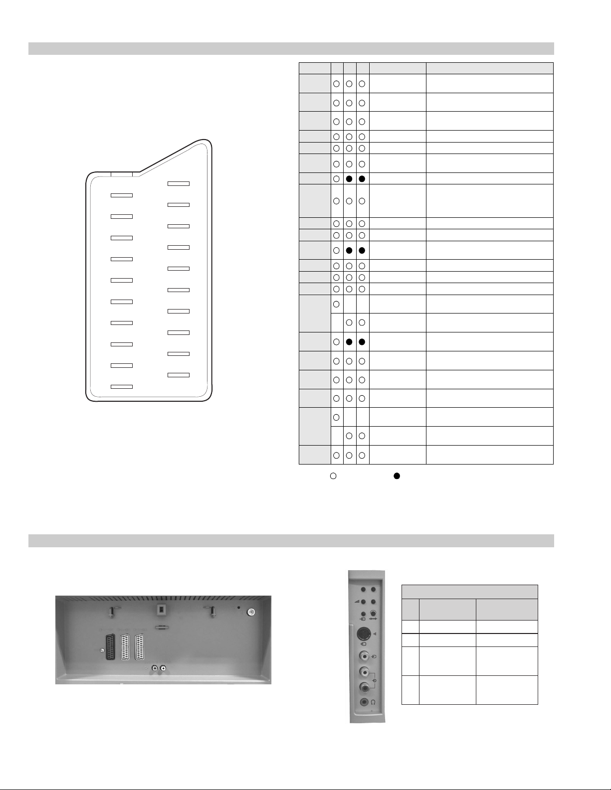
21 pin connector
21
19
17
15
13
11
9
7
5
3
1
20
18
16
14
12
10
8
6
4
2
Pin No 1 2 3 Signal Signal level
1 Audio output B
2
3
4 Ground (audio)
5 Ground (blue)
6 Audio input A
7 Blue input 0.7 +/- 3dB, 75 ohms positive
8 Function select
9 Ground (gre en)
10 Open
11 Green Green signal : 0.7 +/- 3dB, 75 ohms,
12 Open
13 Ground (red)
14 Ground (blanking)
15
_ (S signal Chroma
16 Blanking input
17 Ground (video
18 Ground (video
19 Video output 1V +/- 3dB, 75ohms, positive sync 0.3V
20
_ Video input
21 Common ground
(right)
Audio output B
(right)
Audio output A
(left)
(left)
(AV control)
_ _ Red input 0.7 +/- 3dB, 75 ohms, positive
input)
(Ys signal)
output)
input)
_ _ Video input 1V +/- 3dB, 75ohms, positive sync 0.3V
Y (S signal)
(plug, shield)
Standard level : 0.5V rms
Output impedence : Less than 1kohm*
Standard level : 0.5V rms
Output impedence : More than 10kohm*
Standard level : 0.5V rms
Output impedence : Less than 1kohm*
Standard level : 0.5V rms
Output impedence : More than 10kohm*
High state (9.5-12V) : Part mode
Low state (0-2V) : TV mode
Input impedence : More than 10K ohms
Input capacitance : Less than 2nF
positive
0.3 +/- 3dB, 75 ohms, positive
High state (1-3V) Low state (0-0.4V)
Input impedence : 75 ohms
(-3+10dB)
(-3+10dB)
1V +/- 3dB, 75ohms, positive sync 0.3V
(-3+10dB)
Connected Not Connected (open) * at 20Hz - 20kHz
Rear Connection Panel Front Connection Panel
p
- +
niP
oN
S-Video
socket
4
s
4
4
MONO
L/G/S/I
4
R/D/D/D
1dnuorG2dnuorG3tupni)langisS(Y,mho57Bd3-/+V1
4tupni)langisS(CBd3-/+V3.0
langiS leveLlangiS
noitarugifnocniptekcosoediVS
V3.0.cnySevitisop
Bd01+3-
evitisop,mho57
.cnyS
4
Page 5
AE-5 SELF DIAGNOSTIC SOFTWARE
The identification of errors within the AE-5 chassis is triggered in one of two ways :- 1: Busy or 2: De vice f ailure to respond to IIC. In the e vent of
one of these situations arising the software will first try to release the bus if busy (Failure to do so will report with a continuous flashing LED) and
then communicate with each device in turn to establish if a device is faulty . If a de vice is found to be faulty the relev ant de vice number will be
displayed through the LED (Series of flashes which must be counted) See table 1., non fatal errors are reported using this method.
metIcitsongaiD
noitpircseD
nonruttonseodrewoPthgiltonseoD
)PCO(tnerrucrevOB+semit2
deppotsnoitcelfeDlacitreVsemit4
ybdnatSsemitfooN
sehsalFDEL
.tiucricneposiesuF
egasseMrorrE
rorreoN00
devreseR10
)noitcetorPtnerruCrevO(PCO20
)noitcetorPegatloVrevO(PVO30
noitcetorPlacitreV40
)26TTelbasid
noitcetorPlatnoziroH60
noitcetorPrekaepS70
rorre0subC2I80
redoceD-txeT-eleTB-M90
MVN,23C42TSB-M01
redoceDruoloCniaM,0239ADTB-J11
xoBerutaeFB-2B/1B21
retrevnoC-A/DB-1B31
dnekcaBB-E41
rossecorPdnuoS,D0143PSMB-J51
ediWotuA,7502DXCB-J61
MARlanretxE71
esuacelbaborP
noitacoL
.nideggulptonsidrocrewoP
)draoBD(.detrohssiCIrewoP4066CI
)draoBD(detrohssi0076CI
16TTelbane,s'03retfastratskcehc(BKAelbatsnU
smotpmySdetceteD
noemoctonseodrewoP
VTehtotdeilppussirewopoN
ytluafsiylppusrewopCA
)draoBD(.detrohssi)4086/3086Q(TUO.H
)draoBD(.detrohssi)6086Q(TEFytiraeniL
)draoBD(nepo5386RdeilppustonsiV51+
)draoBD(nepo4386RdeilppustonsiV51-
DEL
sehsalF
50
noemoctonseodrewoP
detrohssahenilrewopnodaoL
deppotssaheslupnoitcelfedlacitreV
detrohssahenilrewoP
Flash Timing Example : e.g. error number 3
StBy LED
ON ON ON
OFF
5
OFF
Page 6

Error Detection Monitor
Device acknowledge is used to check IIC errors. Device ackno wledge is checked by sending an IIC start sequence during CRT power on. Each
device is checked three times, if there is no acknowledge after each attempt, it will be regarded as an error .
There are three steps to check for errors.
1. IIC line 0
If all devices except the NVM have errors, IIC line 0 error is displayed.
2. Board check
If all devices mounted on one board have errors, board error is displayed.
3. Each device check
If IIC line error and board error are not detected then the device with the error is displayed.
The detected errors can be displayed as follows :
1. Error Monitor Menu.
2. Error Reader.
1. Error Monitor Menu
Error Display Mode is entered by the following sequence of commands Standby -> Information -> Digit 5 -> Volume Down -> TV
ERROR MONITOR
1. IGNORE ERRORS OFF ON OFF
Operating Time : 000075 h 15 min
Stored Errors :
1. D1 - B CXA1875 or MB88141
2. No Error Occured
3. No Error Occured
4. No Error Occured
5. No Error Occured
Current Error :
Start Error Sequence
Last menu Enter Item
6
Page 7
2. Error Reader Display
The error reader display is connected to the service connector to read actual error codes. The part number for the error reader display is
S-188-900-10. Once an error has been detected it will then be displayed on the two digit error reader. The erro rs displayed refer to the following
table.
edoCrorrE egasseMrorrE
h000derruccororreoN
h1000CII,rorresuB
h2001CII,rorresuB
h001draoB-A
h101rednapxEtroP,5781AXCB-A
h201renuTniaM,6231UTB-A
h301renuTbuS,0531UTB-A
h002draoB-1B
h102,0829ADS.B-1BxoBerutaeF,456C38PB-1B
h202B-1B
h003 draoB-2B
h103CISEB,7794AAS.B-2B
h203yromeMdleiF,X594AAS.B-2B
h004draoB-3B
h104X-DIM.B-3B
h204amaronaP.B-3B
h304CRD.B-3B
h404retsooBerutciP.B-KB
h005draoB-1D
h105rotrevnoCcimanyD,0708AXCB-1D
h205rednapxEtroP,5781AXCB-1D
h006draoB-E
h106dnekcaB,0012DXCB-E
h007draoB-J
h107ediWotuA,7502DXCB-J
h207PIP,8829ADSB-J
h307redoceDruoloCbuSB-J
h407redoceDruoloCniaMB-J
h507dnuoS-buS,5781AXCB-J
h607reifilpmA-PH,9037ADTB-J
h707hctiwSoiduA,TD2246AETB-J
h807rossecorPdnuoS,D0143PSMB-J
h907PSDdnuoS,F7339CTB-J
hA07hctiwSVA,96X12AXCB-J
h008draoB-M
h108MVN,23C42TSB-M
0829ADS.B-1BxoBerutaeF,456C38P
rotrevnoCA/D
rotrevnoCA/D,
7
Page 8
SECTION 1 GENERAL
Tue 07. 04 .98
10:35 - 12:45
TXT TPS / RINGIER
10:20 - 12:00
10:45 - 10:50
11:00 - 11:20
11:45 - 12:50
Operation
NexTView*
SWISS
Werner - Beinhart
Pro 7
Flui grüsst den Rest der Welt
Kabel 1
Star Wars
Super RTL
12
7
8
9
Tue
Thu
12:38
Index
Wed
full list of selection
personal selection
news broadcasts
movies
07 Tue
a future programme brings you to the long info menu.
NexTView is an electronic programme guide with up to 1 week* of p rogramme info rmation on those chan nels includ ed in
the selected provider.
*If the data exceeds the memory of NexTView, you will get information on less than 7 days.
* depending on availability of service
When looking for information you can search by theme (sports, art etc.), date or time (e.g. broadcasts between 8 and 9 p.m.).
When you’ve found a programme you can go directly to this programme, use the timer to remind you of it or preset your VCR
with Smartlink.
The NexTView provider is responsible for the contents of the guide. The TV set is responsible for the presentation , that is
the menu structure and the navigation, if there is none from the provider. If there is a navigation from the provider the basic
operation with the joystick is the same as described in the Sony navigation.
At first you need to select a channel providing a NexTView service. In this case the indication “NexTView” is displayed
as soon as all data is available. When you later change the channel you can still select this NexTView service.
Operation using the Sony navigation
• moving up or downwards within a column: Use v or V.
• going to the left columns time and date: Use b.
• going to the right column icons: Use B.
• Confirming a selection: Press OK.
(a) while in the columns date, time or icon (themes), the programme list changes according to the selection.
1. Press to switch NexTView on and off.
2. Use the joystick buttons as follows
(b) while in the programme list, confirming a running broadcast brings you dir ectly to the TV programme or con firming
sports
10
Once upon a time in the West
Euronews
Fri
entertainment
International News
RTL Plus
11
12
Sat
children
return to last menu
Fantasy film, USA, 1996
13
Sun
Mon
8
5
3
6
9
2
8
5
0
OK
4
7
1
Italy
France
Language country
Dansk
Čeština
Deutsch
Language
Country
English
Italiano
Español
Français
Select Language: Confirm:
Language country
English
Language
Country
Ireland
Greece
Hungary
Germany
Great Britain
Select Country: Confirm:
:
:
:
:
PROG CH LABEL
Programme Sorting
TV 5
PRO 7
EU-SP
SWF
RTL
SAT
MDR
DDI
C03
C05
C07
C08
C09
C11
C12
C13
1 2 3 4 5 6 7 8 91011
C03 TV 5
DSF
RTL 2
KAB 1
TV 5
PRO 7
EU-SP
SWF
RTL
SAT
MDR
DDI
DSF
RTL 2
PROG CH LABEL
Programme Sorting
C03
C05
C07
C08
C09
C11
C12
C13
1 2 3 4 5 6 7 8 91011
KAB 1
C14
C15
C16
Select Position: Move: OK
C14
C15
C16
Select Prog: Confirm:
The operating instructions mentioned here are partial abstracts from the ‘Operating
Instruction Manual’. The page numbers of the ‘Operating Instruction Manual’ remain
as in the manual.
Installation
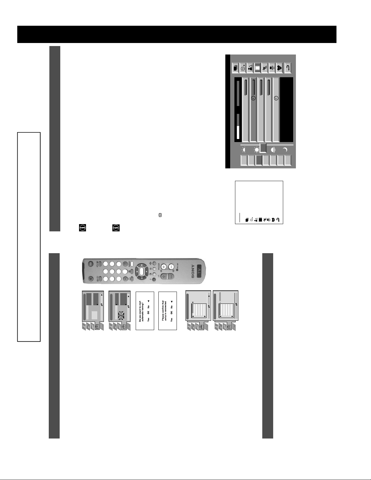
6. Tuning your TV
word ‘English’ highlighted.
chosen language then press the OK button to confirm.
Before you tune your TV, you will be asked to set your language and country.
1. The Language/Country menu appears on the TV screen with the
2. Press the v or V buttons on the remote control to select your
3. Press v or V to select t he country in which you wish to operate
4. The ‘autotune’ menu appears on the TV screen in your selected
5. Ensure the aerial is connected as instructed, then press the OK
want to move, then press B. Press the v or V b uttons to select the
new programme number position for your selected channel then
press the OK button to confirm. The selected channel now moves
to its new programme position and the other channels move
accordingly. Repeat this procedure if you wish to sort the order of
6. Once the TV has tuned all available channels the ‘Programme
other channels on your TV.
7. Press the MENU button to remove the menu from the TV screen.
channels.
8. Press the PROGR+/- or the numbered buttons to view the TV
Note: If you would like to stop the autotune process at any stage,
7. Finding your video channel
If you have connected a VCR to your TV, you now need to find your video channel.
the TV then press the OK button to confirm your choice. Select
press the OK button.
‘OFF’ if you do not want your channels stored in a given channel
sequence starting from programme position 1.
language. Press the OK button to confirm.
button to confirm. The TV starts to automatically search and store
all available channels for you. This may take a few minutes -
please be patient and do not press any buttons.
Sorting’ menu appears on the TV screen enabling you to change
the order of the channel s on your TV. If you wish to change the
channel order, press the v or V buttons to select the channel you
1. Press the PROGR+/- buttons on the TV remote control until your video picture appears on the TV screen.
section of this instruction manual.
Note: If you wish to move your video channel to a different programme position, refer to the ‘Re-arranging the TV channels’
8
Page 9
25
153
101
25
153
101
98
m
m
98
m
TELETEXT
Index
Programme
News
Sport
Weather
Most TV channels broadcast information via Teletext. The index page of the teletext service (usually page 100) gi ves you
information on how to use the service. Please use a TV channel with a st rong signal, otherwise there may be Teletext errors.
T eletext
Operation
Switching Teletext on and off
1. Select the TV channel which carries the teletext service you want to view.
2. Press the button once to get Teletext only.
3. Press twice for Mix mode.
4. Press a third time to switch off Teletext.
Selecting a Teletext page
TELETEXT
Index
Programme
News
Sport
Weather
Input three digits for the page number using the numbered buttons on the remote control. If
you make a mistake, type in any three digits then re-enter the correct page number.
Using Other Teletext Functions
Selecting the next or preceding page
Press the or buttons on the remote control to select the previous or next page.
Selecting a sub page
A teletext page may consist of several sub pages. In this case an information line is displayed,
showing the number of subpages. Select the sub page by pressing v or V.
To freeze a Teletext page
Press the button to freeze the page. Press again to cancel the freeze.
Revealing concealed information
216-02
Press the button to reveal information. Press again to conceal the information.
01 03 04 05 06 07 0802
several page numbers on it (eg the index page).
Using the feature ‘Page Catching’
page is displayed after some seconds.
1. Press the numbered buttons on the remote control to select a teletext page which has
2. Press the OK button.
Using colour buttons to access pages (Fastext)
(only available if the TV station broadcasts Fastext signals)
When the colour coded menu appears at the bottom of a page, press a coloured b utton on the
remote control (green, red, yellow or blue) to access the corresponding page.
3. Press v or V to select the desired page number then press the OK button. The requested
10
9
On
SP
VCR1
Speed
VCR Setup
VPS/PDC
Tue 07. 04 .98
SP
On
VCR1
SWISS TXT TPS / RINGIER nexTView
Address Mapping
The position of the addresses in the
OSDA is shown in the following diagram.
First nextTView/EPG-Providers in Europe
When you select there will be no personal pre-selection. lets you make your own ind ividual selectio n of theme s,
limiting the search to the marked ones.
The menu Individual Settings is displayed.
NexTView*
Operation
Individual Setting
Repeat step 2 for all the items you wish to have in your list.
1. Select using v or V. Push B to enter.
2. Select the item you wish to mark using v or V. Confirm by pressing OK.
3. When finished with the list, select using B and press OK.
Using the ‘Long Info’ menu
The long info menu is displayed.
1. Select a future programme in the column programme list using v or V. Press OK.
The position values of the DPW are set
07 Tue
12:38
to '0'.
If other values are set, the complete
combination will be scrolled.
Example:
if the DPWC is set to '63', the char-
This channel has been set for a timer
Speed
VPS/PDC
Timer Prog
You may wish to record the selected programme with your VCR.
With this setting on, you have the guaranteed recording of the whole broadcast
should there be a change in the TV programme. This only works if the selected
channel broadcasts a VPS/PDC signal.
This information is transferred to the VCR connected to your set.
(only with Smartlink VCRs)
2. Select using b and press OK.
Setting up ypur VCR
3. Select VPS/PDC by pushing b repeatedly.
• Select On or Off using OK.
Select between standardplay (SP) or longplay (LP) mode.With longplay you can
record twice as much on a videotape. The picture quality, however, may suffer.
4. Select Speed using V.
• Select SP or LP using OK.
Select which of the connected Smartlink VCRs you wish to programme.
• Select VCR 1 or 2 using OK.
5. Select VCR Setup using V.
You are back in the last menu.
6. Select using B. Press OK.
9
Page 10

Personal
On
On
Live
Normal
Personal
Movie
On
Off
On
Off
Cool
Warm
Normal
Operation
Using the TV menu system
The TV consists of a menu system which is based on a series of user friendly on -s creen d isplays and men us . Th ese display s will
Picture Adjustment
Picture Mode
Contrast
Brightness
Colour
Sharpness
ResetAINoise Reduction
Colour Tone
Select: Enter:
Picture Mode
Contrast
Noise Reduction
AI
Colour Tone
broadcasting signal.
Personal (for individual settings)
v Movie (for movie broadcasts)
B to enter either the ‘Picture Adjustment’ menu or the ‘Audio Adjustment’ menu.
help you get the most from your TV, helping you to change picture and sound settings, to alter the size of the TV picture and to
rearrange the TV channels etc.
Adjusting the picture and sound
The picture and sound are preset at the factory. You can however adjust them to suit your own taste.
1. Press the MENU button on the remote control to display the menu on the TV screen.
confirm. For a description of the menu items and their effects, see the table below.
2. Press the v or V buttons to select for picture settings or for sound settings then press
3. Press the v or V buttons to select the item on the screen you wish to adjust then press B to
4. Press the v, V, B or b buttons to adjust your selected item.
5. As soon as you have adjusted the item, press the OK button to store the new setting.
Picture Control
Item Effect/Operation
Picture Mode V Live (for live broadcasts)
Contrast Less bB More
Brightness* Darker bB Brighter
Colour* Less bB More
Hue** Reddish bB Greenish
Sharpness* Softer bB Sharper
*Only available if ’Personal’ is selected in ‘Picture Mode’
6. Repeat steps 3-5 if you wish to adjust any of the other items.
7. Press the MENU button to remove the menu from the TV screen.
**Only available for NTSC colour signal (eg. US video tapes)
Reset Resets picture to the factory preset levels
AI V On: Automatic optimization of contrast level
(Artificial Intelligence) according to the TV signal.
v Off: Normal.
Noise Reduction V On: Reduces picture noise in case of a weak
v Off: No noise reduction.
Colour Tone V Warm: Gives a warm tint to the picture.
Normal: Normal.
v Cool: Gives a cool tint to the picture.
12
11
- - : - -– – –
Time Page
PAGE TIME
Teletext
Top / Bottom / Full
Text Clear
Reveal
Time Page
Select: Enter Menu:
Page Overview
Top: Bottom: Full: OK
menu on the TV screen.
Teletext
Operation
Using the Teletext menu
sub menu.
1. With Teletext switched on, press the MENU button on the remote control to display the
2. Press v or V to select your chosen item on the screen then press B to display the relevant
3. To remove the Teletext menu from the screen, press the MENU button.
Top/Bottom/Full
The Top/Bottom/Full sub menu allows you to enlarge different sections of the Teletext page.
Press v to enlarge the upp er half of the screen, Press V to enlarge the lower half. Press the OK
button to restore the page to normal size. Press b to return to the Teletext menu screen.
Text Clear
Text Clear is a function that displays a TV channel while a Teletext page is being searched for.
symbol will appear in the top left hand corner of the screen.
1. Press the button on the remote control to select full screen text.
2. Press the MENU button to display the ‘Teletext’ menu.
3. Press v or V to highlight ‘Text Clear’ and press B to select.
4. The current TV channel is displayed. Once the text page has been found a blue
5. Press the button on the remote control to view the page.
Reveal
Some Teletext pages contain hidden information (eg for a quiz), which can be revealed.
displayed on the screen.
1. In text mode press the MENU button on the remote control to access the ‘Teletext’ menu.
2. Press v or V to highlight ‘Reveal’ and press B to select. The hidden information is
Time Page*
*depending on availability of service.
menu.
is displayed.
1. In Text mode press the MENU button on the remote control to access the ‘Teletext’
2. Press v or V to highlight ‘Time Page’ and press B to select. The ‘Time Page’ sub menu
Time Page allows a time-coded Teletext page (such as an alarm page), to be display ed at a set
time.
3. Enter the desired page number using the numbered buttons on the remote control.
Select Page: 0-9 Next:
displayed in the top left hand corner of the screen. At the requested time the desired p age
is displayed.
Page Overview*
*only available if TOP-Text is transmitted by the TV station.
In this menu the TOP-Text pages are divided into two columns, the first column showing
‘blocks’ of pages and the second showing ‘groups’ of pages.
1. Press b or B to select the first or second column.
4. Enter the desired time using the remote control.
5. Press OK to confirm the settings. The TV will exit Teletext mode and the time will be
2. Press v or V to select the relevant ‘group’ or ‘block’ of pages.
3. Press the OK button to display the chosen pages.
10
Page 11
TV
Off
Off
10 min
Off
On
TV
AV 2
AV 3
AV 4
AV 1
Features
menu.
of the menu items and their effects, see the table below.
1. Press the MENU button on the remote control to display the menu on the TV screen.
2. Press the v or V buttons to select for the ‘Features’ menu then press B to enter the ‘Features’
Using the TV menu system:
Using the Features menu
3. Press the v or V buttons to select the desired menu item then press B to confirm. For a description
Sleep Timer
Parental Lock
AV 2 Output
4. Press the v, V, B or b buttons to select the desired setting.
5. Press the OK button to confirm your choice of setting.
Select: Enter:
Sleep Timer
standby mode.
V Off
v 90 min
6. Repeat steps 3-5 if you wish to select any of the other items.
7. Press the MENU button to remove the menu from the TV screen.
Item Effect/Operation
Sleep Timer You can select a time after which the TV switches itself into
It is only possible to switch the set back on by pressing a button on
v On: This feature disables the TV buttons when the set is in standby mode.
Parental Lock V Off: No parental lock.
Parental Look
the remote control.
AV2 Output V TV audio/video signal from the aerial
AV 2 Output
AV1 audio/video signal from scart 1
AV2 audio/video signal from scart 2
AV3 audio/video signal from scart 3
v AV4 audio/video signal from connectors on front of the TV
Changing the screen size
This feature allows you to change the size of the TV picture.
4:3
Press the button on the remote control repeatedly or use the v or V buttons to select one of the
following formats then press the OK button to confirm your selection:
4:3 conventional 4:3 picture size, full picture information.
16:9 for 16:9 broadcasts.
16:9
14
B
Off
On
Off
v On: Special acoustic effect
On
Auto Vol. Control
broadcast signal.
same independent of the broadcast signal (eg
V On: Volume level of the channels will stay the
Auto Vol. Control v Off: Volume level changes according to the
Mono
Stereo
NICAM
Dual Sound
Volume
in the case of advertisements).
V A for channel 1
v B for channel 2
For a stereo broadcast:
V Mono
v Stereo
When NICAM stereo is being broadcast, the indication NICAM appears br iefly on
Dual Sound For a bilingual broadcast:
Can also adjust the volume level of additional equipment
connected to the RCA sockets on the rear of the TV.
the screen.
Headphones
i Volume Adjusts headphone volume.
Off
Off
Off
Off
Jazz
Rock
Vocal
Personal
Audio Adjustment
Using the TV menu system:
Sound Control
Item Effect/Operation
Equaliser Mode
Equaliser
Adjustment
Vocal
Equaliser Mode V Personal
0
Balance
Loudness
Stereo
NICAM
Space
Auto Vol. Control
Dual Sound
Jazz
Rock
Stereo
Confirm: OK
NICAM
Select Mode :
Volume
Dual Sound
Pop
v Flat (fixed setting, cannot be adjusted)
cutting and boosting the 5 selected frequency bands.
Equaliser adjustment You can adjust the mode selected in Equaliser mode by
(Personal)
Equaliser Adjustment
0
+
Press b or B to select the frequency band then V or v to
adjust the frequency. Finally, press the OK button to store
the new adjustment.
120 150 1,5K 5 K 10 K
–
If you want to store the new setting, you need to set the Equali ser mode to
Sel: Adjust: Confirm:OK
‘Personal’. Personal mode permanently stores the setting, all other modes (Vocal,
Jazz, Rock, Pop) store only until the next mode change.
0
Balance
Balance b More left
On
Space
Loudness
B More right
v On: For music broadcasts
Loudness V Off: Normal
Space V Off: Normal
A
NICAM
Dual Sound
V A for channel 1
v B for channel 2
i Dual Sound For a bilingual broadcast:
13
11
Page 12
Manual Set Up
Manual Set Up
Language/Country
Language/Country
Manual Programme Preset
Manual Programme Preset
O
RGB Set Up
Picture Rotation
Further Programme Preset
RGB Set Up
Further Programme Preset
O
- - - - - - -
- - - - - - -
Personal ID
Demo
Picture Rotation
Personal ID
Demo
O
Manual Set Up
Language/Country
Manual Set Up
Language/Country
Manual Programme Preset
Manual Programme Preset
O
RGB Set Up
Picture Rotation
Further Programme Preset
RGB Set Up
Picture Rotation
Further Programme Preset
- - - - - - -
- - - - - - -
Personal ID
Demo
Personal ID
Demo
BBC1
BBC
C09
C10
I
I
Off
Off
Off
Off
Off
Off
Off
Off
Select: Enter:
Select: Enter:
5152535455565758596061
Manual Programme Preset
PROG CHSYSSKIP LABEL
F189 - - - Off
Off
Off
On
Off
53 I
Select: Enter:
PROG CHSYSSKIP LABEL
17
ARD
BBC
C09
C10
B/G
B/G
Off
Off
Off
Off
Off
Off
Off
Off
Off
Select: Enter:
Select: Enter:
1 2 3 4 5 6 7 8 91011
Manual Programme Preset
PROG CHSYSSKIP LABEL
C07 TE
Off
Off
Off
SKIP LABEL
6 I
Select: Enter:
PROG CHSYS
Using the TV menu system:
Naming a channel
Names for channels are usually taken automatically from Teletext if available. You can however name a channel or an input
Set Up
video source using up to five characters (letters or numbers).
Auto Tuning
1. Press the MENU button on the remote control to display the menu on the TV screen.
- - - - -
Programme Sorting
Select NexTView
AV Preset
Manual Set Up
Select: Enter :
2. Press the V button to select the symbol on the menu screen then press B to enter the ‘Set
Up’ menu.
PROG CH LABEL
Programme Sorting
menu.
3. Press the V button to select ‘Manual Set Up’ then press B to enter the ‘Manual Set Up’
TV 5
PRO 7
EU-SP
SWF
RTL
SAT
MDR
DDI
C03
C05
C07
C08
C09
C11
C12
C13
1 2 3 4 5 6 7 8 91011
This function enables you to skip unused programme positions when selecting them with the PROGR+/- buttons.
- - - - -
Select Next View
AV Preset
Skipping programme positions
Manual Set Up
However, by using the number buttons you can still select the skipped programme position.
O
- - - - - - -
Manual Set Up
RGB Set Up
Picture Rotation
Personal ID
Further Programme Preset
Language/Country
Manual Programme Preset
Select: Enter :
Programme Preset’ menu.
4. Press the V button to select ‘Manual Programme Preset’ then press B to enter the ‘Manual
5. Press the v or V buttons to select the channel you wish to name.
C03 TV 5
DSF
RTL 2
KAB 1
TV 5
PRO 7
EU-SP
SWF
C14
C15
C16
RTL
C03
C05
C07
C08
C09
1 2 3 4 5 6 7 8 91011
PROG CH LABEL
Programme Sorting
Select Prog: Confirm:
confirm. Select the other four characters in the same way.
6. Press the B button repeatedly until the first element of the ‘LABEL’ column is highlighted.
7. Press the v or V buttons to select a letter or number (select ‘-’ for a blank) then press B to
8. After selecting all the characters, press the OK button.
9. Repeat steps 5 to 8 if you wish to label other channels.
10.Press the MENU button to remove the menu from the TV screen.
SAT
MDR
DDI
DSF
RTL 2
KAB 1
C11
C12
C13
C14
C15
C16
Select Position: Move: OK
Set Up
Auto Tuning
Programme Sorting
‘Set Up’ menu.
menu.
Programme Preset’ menu.
‘SKIP’ column.
1. Press the MENU button on the remote control to display the menu on the TV screen.
2. Press the V button to select the symbol on the menu screen then press B to ente r the
3. Press the V button to select ‘Manual Set Up’ then press B to enter the ‘Manual Set Up’
4. Press the V button to select ‘Manual Programme Preset’ then press B to enter the ‘Manual
ARD
BBC
TV 5
PRO 7
EU-SP
SWF
RTL
SAT
MDR
DDI
DSF
C03
C05
C07
C08
C09
C11
C12
C13
C14
C09
C10
B/G
B/G
B/G
B/G
B/G
B/G
B/G
B/G
B/G
Off
Off
Off
Off
Off
Off
Off
Off
Off
1 2 3 4 5 6 7 8 91011
Select: Enter:
Manual Programme Preset
PROG CHSYSSKIP LABEL
Demo
I
L
D/K
B/G
B/G
B/G
Off
Off
EXT
Off
SKIP LABEL
Select: Enter:
1
PROG CHSYS
5. Press the v or V buttons to select the programme position then press B to highlight the
CH
SKIP LABEL
PROG SYS
position) then press the OK button to store.
6. Press the v or V buttons to select ‘Off’ or ‘On’ (if you wish to skip this programme
7. Repeat steps 5 and 6 if you wish to skip or unskip further programme positions.
8. Press the MENU button to remove the menu from the TV screen.
AV1
03
SEARCH
CH
AV1
AV2
F
S
C
Off
1 I
AV3
Off
SKIP LABEL
Off
SKIP LABEL
1 I
0 EXT
PROG SYS
PROG CHSYS
You have already tuned the TV automatically using th e instructions at the start of this manual. You can however carry out
Manually tuning the TV
this operation manually, adding channels to the TV, one at a time.
menu.
Set Up’ menu.
the ‘Manual Programme Preset’ menu.
1. Press the MENU button on the remote control to display the menu on the TV screen.
then press B to highlight the ‘SKIP’ column.
2. Press the V button to select the symbol on the menu screen then press B to enter the ‘Set Up’
3. Press the V button to select ‘Manual Set Up’ on the menu screen then press B to enter the ‘Manual
4. Press the V button to select ‘Manual Programme Preset’ on the menu screen then press B to enter
5. Press the v or V buttons to select a prog ramme numbe r for your channel (eg PROGR 1 for BBC1)
(AV1, AV2, ...) then press B to confirm.
direct frequency inputs then press B to confirm.
number buttons on the remote control or
Press the V button to search for the next available channel.
6. Press v to select ‘OFF’ then press B to highlight the ‘SYS’ column.
buttons to continue searching for the desired channel.
7. Press the v or V buttons to select the TV broadcast system or ‘EXT’ for a video input source
8. Press the v or V buttons to select ‘C’ for terrestrial channels, ‘S’ for cable channels, or ‘F’ for
9. Select the first number digit of ‘CH’ (channel) then the second number digit of ‘CH’ with the
10.If you do not wish to store this channel on the programme number you selected, press the v or V
menu from the TV screen.
11.If this is the channel you wish to store, pres s the OK button.
16
12.Repeat steps 5-11 if you wish to store more channels then press the MENU button to remove the
After tuning the TV, you can use this feature to change the order of the channels on the TV.
Using the TV menu system:
Re-arranging the TV channels
menu.
1. Press the MENU button on the remote control to display the menu on the TV screen.
2. Press the V button to select the symbol on the menu screen then press B to enter the ‘Set Up’
menu.
3. Press the V button to select ‘Programme Sorting’ then press B to enter the ‘Programme Sorting’
channel then press the OK button to confirm. The selected channel now moves to its new
programme position and the other channels move accordingly.
4. Press the v or V buttons to select the channel you want to move then press B to confirm.
5. Press the v or V buttons to select the new programme position (eg PROG 4) for your selected
6. Repeat steps 4 and 5 if you wish to sort the other channels.
7. Press the MENU button to remove the menu from the TV screen.
12
Page 13
- - - - -
O
O
O
19
Using the TV menu system:
Because of the earth’s magnetism the picture might slant. In this case you can readjust the picture.
Adjusting the picture rotation
Set Up
RGB Set Up
Manual Programme Preset
RGB Set Up
Further Programme Preset
Picture Rotation
Personal ID
Demo
Rotate: Confirm: OK
Manual Set Up
Select: Enter:
AV Preset
Manual Set Up
Auto Tuning
Programme Sorting
Select Next View
Language/Country
H CentreOH Size
RGB Set Up
Adjust Position: Confirm: OK
H CentreOH Size
Adjust Size: Confirm: OK
1
‘Set Up’ menu
menu.
sub menu.
1. Press the MENU button on the remote control to display the menu on the TV screen.
2. Press the V button to select the symbol on the menu screen then press B to enter the
3. Press the V button to select ‘Manual Set Up’ then press B to enter the ‘Manual Set Up’
button to store.
4. Press the V button to select ‘Picture Rotation’ then press B to enter the ‘Picture Rotation’
5. Press the v or V buttons to rotate the picture over a range of -5 to +5 then press the OK
6. Press the MENU button to remove the menu from the TV screen.
When connecting an RGB source such as a Sony Playstation you may need to readjust the geometry of the picture.
Adjusting the picture geometry for an RGB source
1. Press the button on the remote control to select the connected RGB source .
Up’ menu
‘Manual Set Up’ menu
‘RGB Set Up’ sub menu.
of -10 to +10. Store the new range by pressing the OK button.
2. Press the MENU button to display the menu on the TV screen.
3. Press the V button to select the symbol on the menu screen then press B to enter the ‘Set
4. Press the V button to select ‘Manual Set Up’ on the menu screen then press B to enter the
5. Press the V button to select ‘RGB Set Up’ on the menu screen then press B to enter the
of -10 to +10. Store the new range by pressing the OK button.
6. Press B to select H Centre then press v or V to adjust the centre of the picture over a range
7. Press B to select H Size then press v or V to adjust the horizontal coordinates over a range
8. Press the MENU button to remove the menu from the TV screen.
Using the TV menu system:
With this feature you can a) adjust the attenuation of each channel, b) individually adjust the volume level of each channel,
Using the Further Programme Preset feature
Off
AV1
PROG AFTVOL DECODER
Press the v or V buttons to adjust the volume level (range -7 to +7) of the channel. Store by
AV2
On
1 -5
1 -5 On
PROG AFTVOL DECODER
pressing the OK button. Repeat steps 5 and 6b if you wish to adjust the volume level of the
other channels.
c) AFT - Automatic Fine Tuning
Press the v or V buttons to fine tune the channel frequency over a range of -15 to +15. Press
the OK button to confirm. Repeat steps 5 and 6c if you wish to fine tune other channels.
d)DECODER
Press the v or V buttons to select AV1 or AV2 for the programme position then press the OK
button to confirm. You can now attach a decoder to the AV1 or the AV2 socket on the back of
the TV and the picture from that decoder will appear on this programme number. Repeat steps
5 and 6d to preset the AV output for other programme positions.
7. Press the MENU button to remove the menu from the TV screen.
This function provides an overview of some of the features available on the TV.
Selecting the ‘Demo’ feature
- - - - -
Select: Enter:
AV Preset
Manual Set Up
Auto Tuning
Programme Sorting
Select Next View
Set Up
‘Set Up’ menu
1. Press the MENU button on the remote control to display the menu on the TV screen.
2. Press the V button to select the symbol on the menu screen then press B to enter the
3. Press the V button to select ‘Manual Set Up’ then press B to enter the ‘Manual Set Up’
menu.
Manual Set Up
Language/Country
Manual Programme Preset
Further Programme Preset
4. Press the V button to select ‘Demo’ then press B to start the demonstration (which lasts for
O
Start
- - - - - - -
RGB Set Up
Picture Rotation
Personal ID
Demo
approximately 5 minutes).
Select: Enter:
5. Press the button to remove the demonstration from the TV screen.
18
O
- - - - - - -
Manual Set Up
c) manually fine-tune the TV to obtain a better picture reception if the picture is distorted or d) preset the AV output for
the programme positions of channels with scrambled signals (eg from a pay TV decoder). In this way a connected VCR
records the unscrambled signal.
Select: Enter:
Language/Country
Manual Programme Preset
Further Programme Preset
RGB Set Up
Picture Rotation
Personal ID
Demo
Up’ menu
1. Press the MENU button on the remote control to display the menu on the TV screen.
2. Press the V button to select the symbol on the menu screen then press B to enter the ‘Set
3. Press the V button to select ‘Manual Set Up’ then press B to enter the ‘Manual Set Up’ menu.
4. Press the V button to select ‘Further Programme Preset’ then press B to enter the ‘Further
ATT
Further Programme Preset
PROG AFTVOL DECODER
Programme Preset’ menu.
Off
Off
Off
Off
Off
Off
Off
Off
OnOnOnOnOn
OnOnOn
000
000
000
Off
Off
Off
Off
Off
Off
Off
Off
1 2 3 4 5 6 7 8 91011
repeatedly to select a) ATT b) VOL c) AFT or d) DECODER. The selected item changes
5. Press the v or V buttons to select the relevant programme number then press the B button
Off
Off
Off
On
On
On
0
0
Off
Off
Off
Select: Enter:
colour.
PROG AFTVOLATT DECODER
Press the v or V buttons to switch attenuator ‘on’ or ‘off’. Press the OK button to confirm the
0
Off
On
1
1
PROG AFTVOL DECODER
selection. Repeat steps 5 and 6a if you wish to adjust the attenuation of the other channels.
b)VOL - Volume Offset
6. a)ATT - RF Attenuator
13
Page 14
Additional Information
Troubleshooting
Here are some simple solutions to problems which may affect the picture and sound.
/
button on the remote control.
• Press the button on the front of the TV.
• If the indicator is on press the button or a numbered
Problem Suggested remedy
No picture (screen is dark), no sound • Plug the TV in.
using the button on the front of the TV.
Adjustment display. Adjust the brightness, picture and colour
balance levels.
to the factory settings.
remote control.
display and adjust the colour setting.
to the factory settings.
• Check the aerial connection.
• Turn the TV off for 3 or 4 seconds and then turn it on again
• Using the MENU system, select the Picture
• From the Picture Adjustment display select RESET to return
• Press the button on the remote control.
• If is displayed on the screen, press the button on the
Poor or no picture (screen is dark), but
good sound.
Good picture, no sound
No colour on colour programmes • Using the MENU system, select the Picture Adjustment
the rear of the TV.
• From the Picture Adjustme nt display select RESET to return
• Turn off any equipment connected to the scart connectors on
Distorted picture when changing
• Contact your nearest Sony service centre.
• Reduce sharpness level.
programmes or selecting Teletext
Remote control does not function • Replace the batteries.
The standby indicator on the TV
flashes
Interference on picture from external
equipment
• If you continue to have these problems, have your TV serviced by qualified personnel.
• NEVER open the casing yourself.
24
Specifications
Additional Information
Sound output
Left/Right: 2x20W (Music Power)
TV system
B/G/H, D/K
2x10W (RMS)
15W (RMS)
Sub woofer: 30W (Music Power)
Colour system
PAL, SECAM
Power consumption
121W
Dimensions (wxhxd)
Approx. 771x585x506mm
Weight
Approx. 51kg
Accessories supplied
RM-887 remote control (1)
IEC designated size AA batteries (2)
Optional accessory
TV Stand: SU-29FX2
Other features
Flat display Trinitron tube, noise reduction, graphic equaliser,
2000 page TEXT memory, personal ID, sleep timer,
NexTView.
Design and specifications are subject to change
without notice.
Receivable Channels Channel Displays
video input, RGB input, TV audio/video output.
video input, S-video input, Selectable audio/video output.
video input, S-video input, Monitor audio/vi deo output.
1
2
3
s
s
/ 21-pin Euro connector (CENELEC standard) including audio/
/ 21-pin Euro connector (CENELEC standard) including audio/
/ 21-pin Euro connector (CENELEC standard) including audio/
2
3
NTSC 3.58, 4.43 (only Video In)
Channel coverage
See the ‘Channel Display Table’ below.
Picture tube
FD Trinitron, Appro x. 72cm (29 inches)
Rear Terminals
1
L/G/S/I RCA connectors, variable output for audi o signals.
R/D/D/D
RF In
Video input -phono jacks
Audio inputs - phono jacks
S video input - 4 pin DIN
Headphones jack - minijack stereo
4
4
4
s
Front Terminals
Channel Display Table
B/G/H E2..12, 21..69 C02..C12, C21..69
M1..M10 S01..S10
U1..U10 S11.S20
KABEL-TV (1) S1..S41 S01..S41
KABEL-TV (2) S01..S05 S42..S46
S01..S05 S42..S46
ITALIEN A, B..H, H1, H2 C13, C14..C20, C11, C12
D/K R01..R12, R21..R69 C01..C12, C21..C69
22
14
Page 15
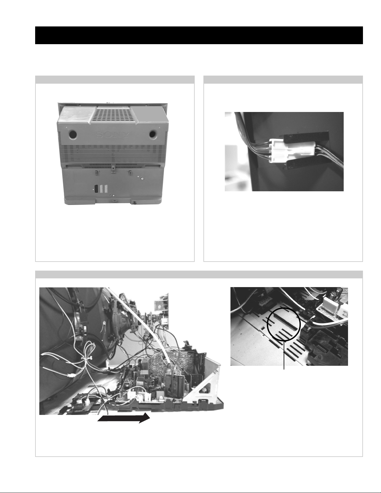
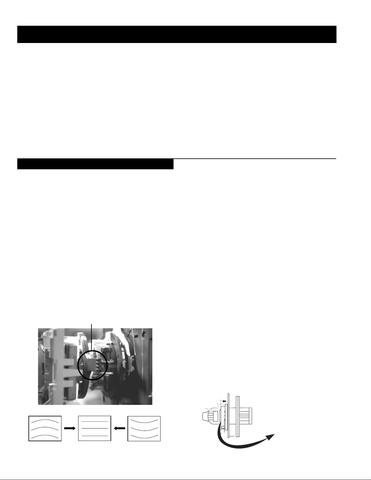
SECTION 2 DISASSEMBLY
2-1. Rear Cover Removal
<=
<=
=>
<=
=>
Remove the rear cover f ixing screws indicated. Take care
when removing the rear cover not to damage the speaker
cables [Disconnect the speaker connector] as speakers are
fitted inside the rear cover .
=>
<=
2-2. Speaker Connector Disconnection
<=
Before completely removing the rear cover disconnect the
speaker connector which is located on the inside.
2-3. Chassis Removal and Refitting
T o remove lift the main bracket rear slightly and slide the
chassis away from the beznet. Ensure that the interconnecting
leads are released from their purse locks to prevent damage
being caused.
When refitting the chassis ensure that the main
bracket is located in the beznet guide slots before
sliding the chassis forwards. Refit the
interconnecting leads in their respective purse locks.
15
Page 16
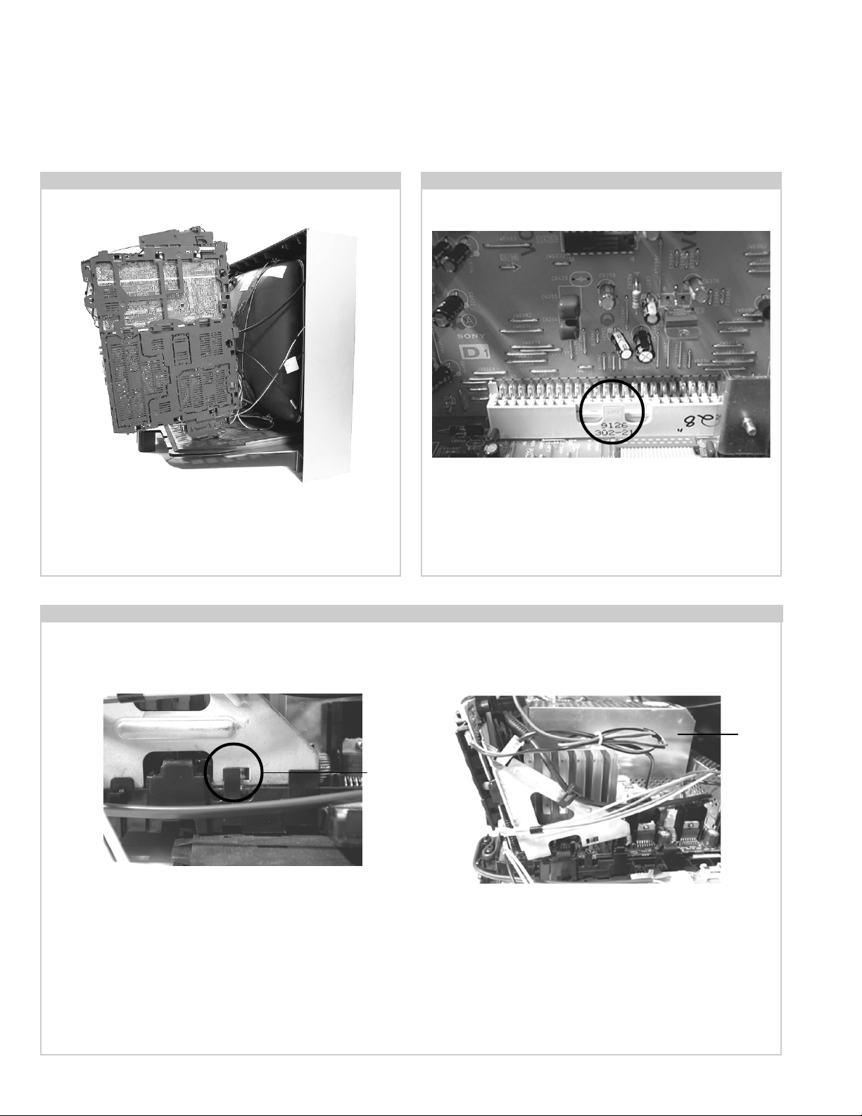
2-4. Service Position 2-5. D1 Board Removal
Position the PWB as indicated to access the solder side.
T o gain access to the D Board follo w the instructions on page
19. [Removal and Replacement of the main bracket bottom
plates ].
2-6. J Board Removal
T o remove the D1 Board release the clip circled and gently
remove the board in a vertical direction.
Shield
case
Clip
Release the two metal bracket support clips located on either side of the chassis. Tilt the bracket very slightly away from the shield
case indicated. Release the J board board socket retaining clip and carefully lift the complete assembly vertically .
16
Page 17
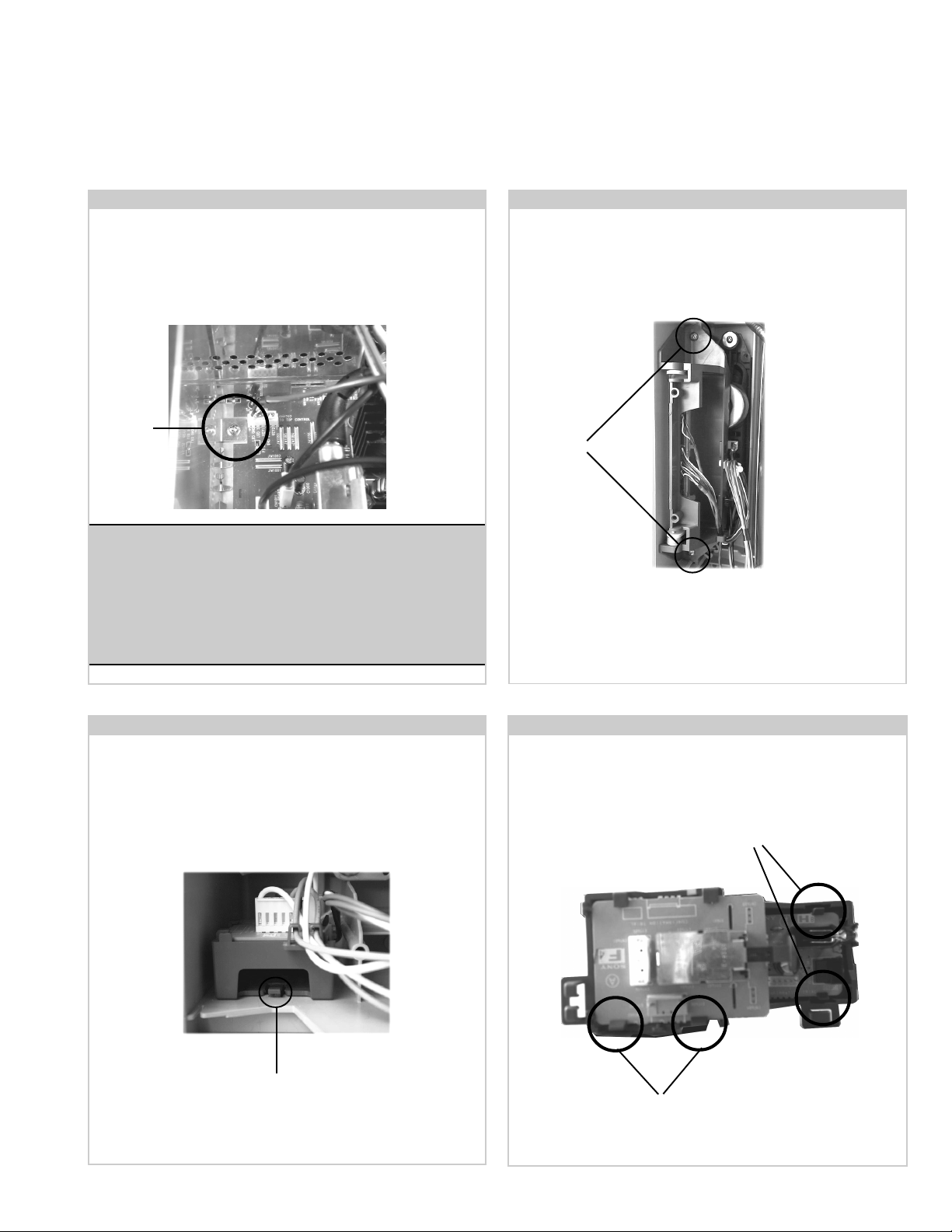
Follow the steps indicated in removal of the J board. With the
assembly removed access to the B2 board shield is possible. To
remove the shield locate and remove the two screws positioned on
either side and at opposite ends of the shield. Release the B2 board clip
and remove in a vertical direction. Please ensure that the screws are
refitted after service.
Screw
Note :
Removal of the B2, E, and M1 printed circuit boards follows the
same procedure of releasing the securing clips as indicated
in the fig for D1 board removal.
T ake care not to apply to great a pressure to the clips as this may
cause damage.
2-8. Side Control Module Removal2-7. B2 Board Removal
Remove the two screws fixing the user control module to the
side of the set. The control module can then be removed by
sliding it towards the rear of the set allowing access to the H7
Board.
Screws
2-9. F4 Bracket Removal
Rrelease the clip circled and pull the bracket towards the rear
of the set. The bracket can then be removed to allow access to
the boards.
Clip
2-10. F4 and H8 Board Removal
T o remove the F4 and H8 Boar ds release the clips circled and
ease the boards gently away from the support bracket.
Clips
Clips
17
Page 18
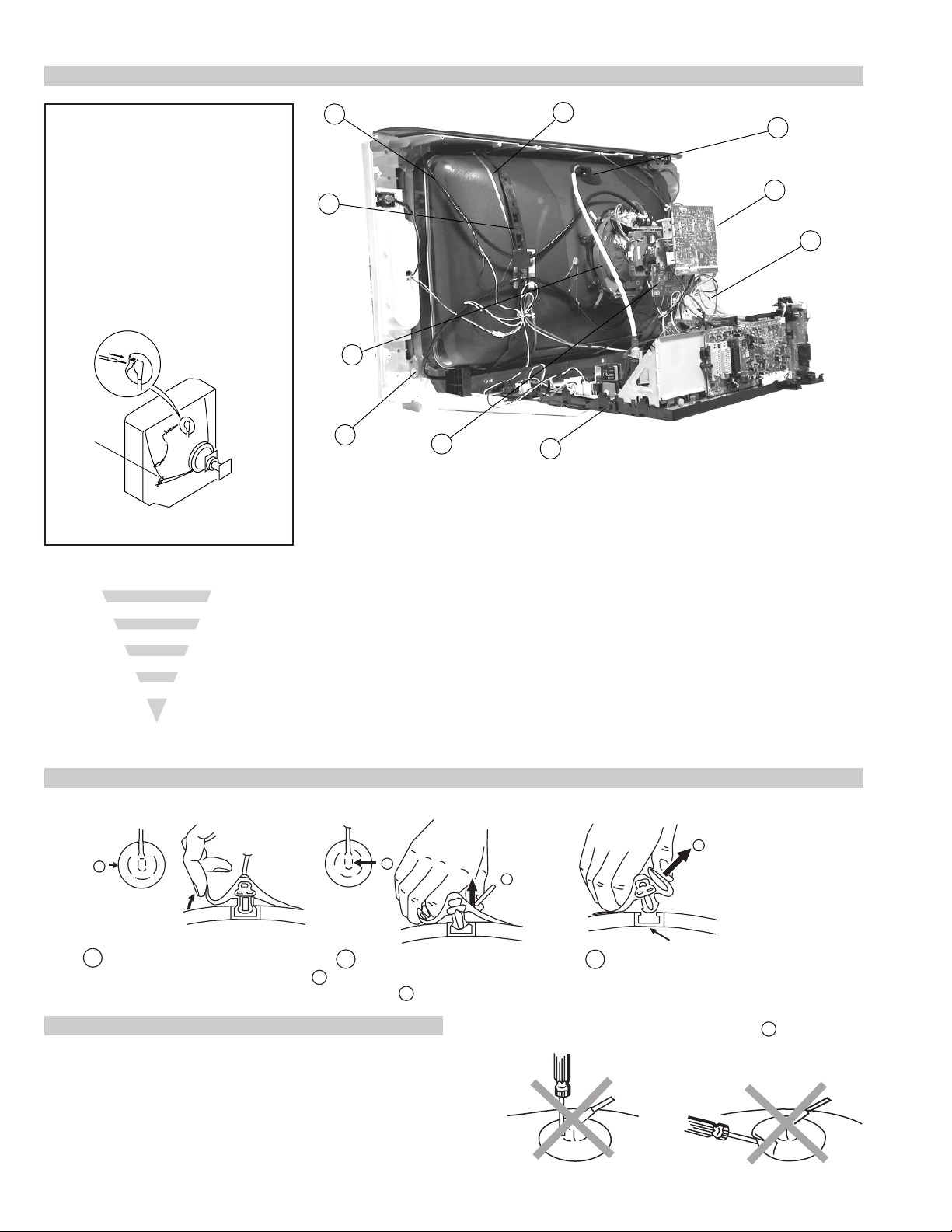
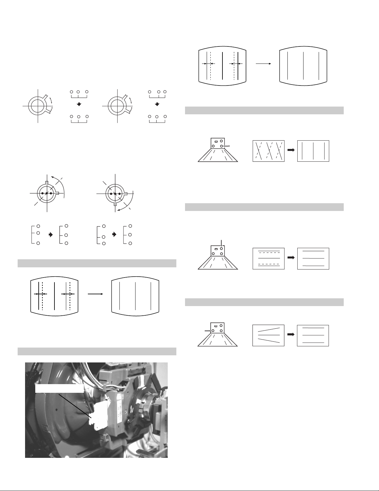
2-11. Picture Tube Removal
WARNING:
BEFORE REMOVING
THE ANODE CAP
High voltage remains in the CRT even
after the power is disconnected. To
avoid electric shock, discharge CRT
before attempting to remove the anode
cap. Short between anode and CRT
coated earth ground strap.
Coated Earth
Ground Strap
8
9
1
3
7
2
6
10
5
4
1. Discharge the anode of the CR T and remove the anode cap.
2. Unplug all interconnecting leads from the Deflection yoke, neck
assy, de gaussing coils and CRT grounding strap.
3. Remove the C Board from the CR T.
4. Remove the chassis assembly .
5. Loosen the Neck assembly fixing screw and remove.
6. Loosen the Deflection yoke fixing screw and remove.
7. Place the set with the CR T face do wn on a cushion and remove
the Degaussing Coil holders.
8. Remove the Degaussing Coils.
9. Remove the CR T grounding strap and spring tentioners.
10. Unscrew the four CRT fixing screws [ located on each CR T
corner ] and remove the CR T .
[T ake care not to handle the CR T by the neck.]
Removal of the Anode-Cap
* REMOVING PROCEDURES.
a
1
Turn up one side of the rubber cap in
the direction indicated by the arrow a
b
2 Using a thumb pull up the rubber cap
firmly in the direction indicated by the
arrow b
How to handle the Anode-Cap
1. To prevent damaging the surface of the anode-cap do not use
sharp materials.
2. Do not apply too great a pressure on the rubber, as this may cause
damage to the anode connector.
3. A metal fitting called a shatter hook terminal is fitted inside the
rubber cap.
4. Do not turn the rubber foot over excessively, this may cause damage
if the shatter hook sticks out.
c
b
Anode button
3 When one side of the rubber cap is
separated from the anode button, the
anode-cap can be removed by turning
up the rubber cap and pulling it up in
the direction of the arrow c
18
Page 19
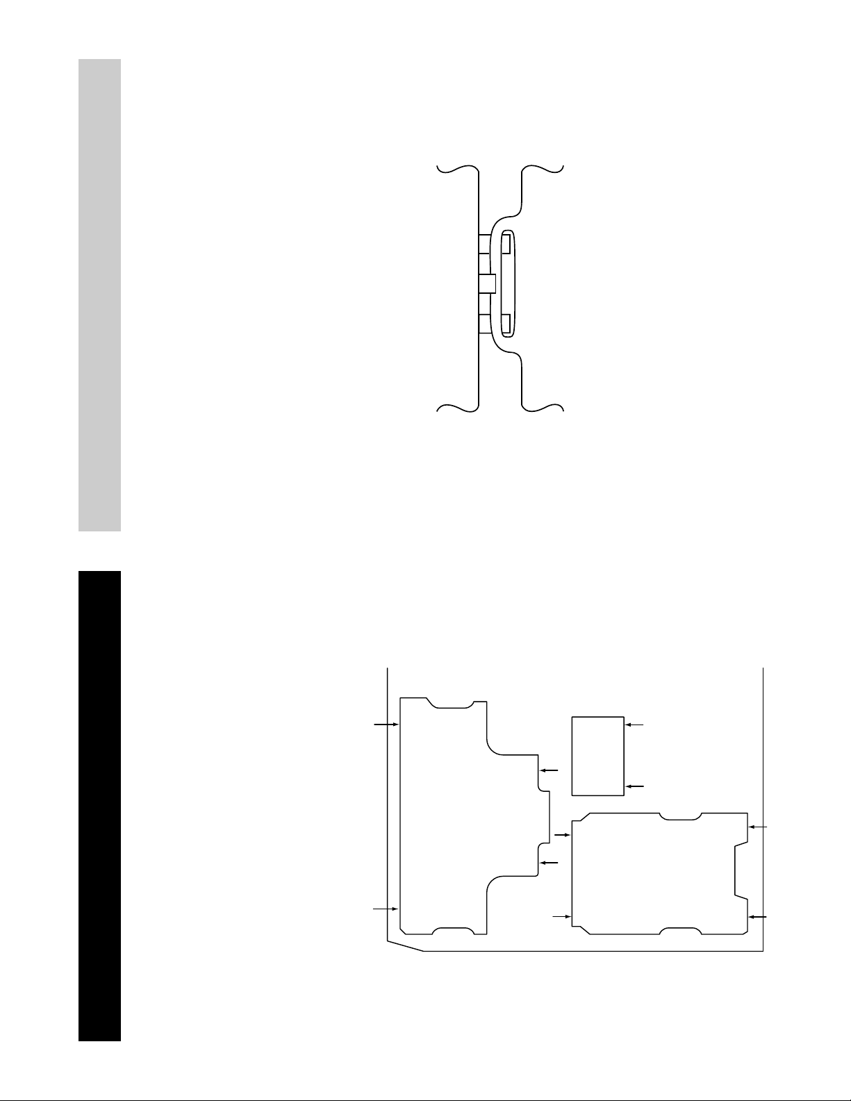
For safety reasons, on no account should the plates be
removed and not refitted after servicing.
£
Because the plates differ in size it is important that the correct plates are refitted in their original
location.
Please note that the plates need to be rotated 180 degrees from their cut position to allow the
(2) REFITTING THE PLATES
tabs to be fitted into their catch positions.
Catch
Tab
REMOV AL AND REPLA CEMENT OF THE MAIN-BRACKET
BOTT OM PLA TES.
Only remove the necessary plate to gain access to the printed wiring board.
In the event of servicing being required to the solder side of the D Board printed wiring board,
the bottom plates fitted to the main chassis bracket require to be removed.
This is performed by cutting the gates with a sharp wire cutter at the locations indicated by the
arrows.
(1) REMOVING THE PLATES
Note : There are 3 plates fitted to the main bracket and secured by3 gates.
19
Page 20
SECTION 3 SET -UP ADJUSTMENTS
• When complete readjustment is necessary or a new picture tube is
installed, carry out the following adjustments.
• Unless there are specific instructions to the contrary, carry out
these adjustments with the rated power supply .
• Unless there are specific instructions to the contrary, set the
controls and switches to the following settings :
Contrast .................................. normal
Brightness .................................. normal
3-1. Beam Landing
Preparation :
1. In order to reduce the influence of geomagnetism on the set’s
picture tube, face it in an easterly or westerly direction.
2. Switch on the TV set’s power and deg auss with a de gausser.
(1) Adjustment of Correction Magnet for Y-Splitting Axis.
1. Input a crosshatch signal from the pattern generator.
2. Set the Picture control to minimum and confirm that the
Brightness control is set to normal.
3. Position the neck assembly as indicated in Fig.3-3.
4. Loosen the deflection yoke fixing screw .
5. Move the deflection yoke as far forward as is possible.
6. Adjust the upper and lower pin symmetrically by opening or
closing the Y -splitting axis cor rection magnets located on the neck
assembly. [See Fig 3-1 and Fig 3-2]
7. Return the deflection yoke to its original position and re-tighten its
fixing screw.
Fig.3-1
Y-splitting axis correction magnet
Carry out the adjustments in the following order :
3-1. Beam Landing.
3-2. Convergence.
3-3. Focus.
3-4. White Balance.
Note : Test equipment required.
1. Color bar/pattern generator .
2. De gausser .
3. Oscilloscope.
4. Digital multimeter .
Caution :
High voltages are present on the Deflection yoke terminals - take care
when handling the Deflection yoke whilst carrying out adjustments.
(2) Landing
Note : Before carrying out the following adjustments adjust the
magnets as indicated below [See Fig.3-4].
1. Input a crosshatch signal from the signal generator.
2. Rough-adjust the focus and horizontal convergence.
3. Switch from the crosshatch pattern to an all-red pattern.
4. Move the deflection yoke backwards and adjust with the purity
magnet so that the red is at the centre and it aligns
symmetrically [See Fig.3-5].
5. Move the deflection yoke forward to the point where the entire
screen just becomes red [Mark its position].
6. Move the deflection yoke further forward until the screen just
changes colour at the edges. [Mark its position]
7. Position the deflection yoke between the two marks indicated
above.
8. Input a crosshatch pattern from the pattern generator and rotate the
deflection yoke so that the horizontal lines are parallel with the top
and bottom of the screen.
9. When the position of the deflection yoke has been determined,
fasten it with its fixing screw.
10. Switch the pattern generator to green then blue and confirm the
purity.
11. If the beam does not land correctly in all the corners of the screen,
use disk magnets to correct it. [Confirm the corner landing for
green and blue]
Fig.3-2
20
Fig.3-3
G1
G2
+
G3
Neck assy
Align the edge
of the neck assy with
the edge of the G2 grid
on the G3 side.
Page 21
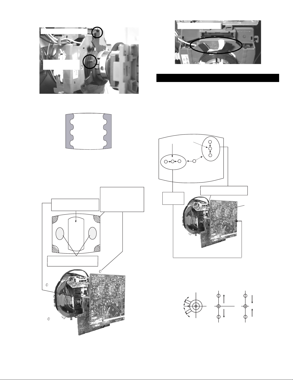
Fig.3-4
Purity magnets
Align pips on
each magnet
GREEN
RED
Align both Purity magnets
to the vertical position
BLUE
Purity control magnets
3-2. Con vergence
(1) Screen centre convergence [Static convergence]
1. Input a dot pattern signal from the pattern generator .
2. Normalize the picture setting.
3. [Moving vertically], adjust the V.STAT magnet so that the
vertical red, green and blue dots coincide at the centre of the
screen.
Center dot
R
G
B
Fig.3-5
Purity control corrects
this area
a
cd
b
Deflection yoke positioning
corrects these areas
Disk magnets or
rotatable disk
magnets correct
these areas (a-d)
R
G
B
H STAT
convergence
control
V.STAT Vertical Static Magnet
C Board
RV5375 (H STAT)
H STAT Convergence
(on mount side)
By opening or closing the V.ST AT magnet, the red green and blue
dots move in the direction indicated below.
B
B
Disk Magnets
G
R
Note: Do not adjust the H.STAT by rotating the V.STAT
magnets as this can affect the focus setting.
21
G
R
Page 22
4. Correction for HMC [Horizontal mis-conver gence] and VMC
[V ertical mis-con ver gence] by using the BMC [Hexapole] magnet.
a). HMC correction by BMC [Hexapole] magnet and movement of
the electron beam.
HMC correction(A) HMC correction(B)
A > B
A < B
RG B
RGB
HTIL correction can be performed by adding a THL correction
assembly to the Deflection yoke.
A = B
RG B
A = B
RG B
b). VMC correction by BMC [Hexapole] magnet and movement of
the electron beam.
VMC correction(A) VMC correction(B)
C < D
C
D
C = D C > D C = D
R
G
B
R
C
G
D
B
R
G
B
R
G
B
HAMP Adjustment
YCH Adjustment
+
+
+
YCH VR
Deflection Yoke
TL V Adjustment
TLV VR
+
+
+
Deflection Yoke
Adjust the HAMP using HAMPL and HAMPR registers in the
Dynamic Convergence section of the service menu.
HTIL Adjustment
THL Correction assy
H-TRAP Adjustment
+
+
HTRAP VR
+
Deflection Yoke
The H-TRAP should not be adjusted unless absolutely necessary as it
affects the TLV settings.
22
Page 23
Layout of each control
Purity magnet
BMC (Hexaploe) magnet
V STAT convergence magnet
Y-splitting axis correction magnet
3-3. Focus, Screen (G2) Adjustment
1. Receive a television broadcast signal.
2. Normalize the picture setting.
3. Adjust the focus control located on the flyback transformer to
obtain the best focus at the centre of the screen.
Bring only the centre area of the screen into focus, the magentaring appears on the screen. In this case, adjust the focus to
optimize the screen uniformly.
Note : If you are unable to adjust the corner converg ence properly ,
this can be corrected with the use of permalloy magnets.
a
a-d: screen-corner
convergence defect
c
Install the permalloy assembly
for the area that needs correcting.
b
d
a
b
Permalloy Assy
X-4387-214-1
c
d
Convergence adjustment with permalloy
Focus
Control
No
Function
G2 adjustment [RV5376]
1. Input a dot signal from the pattern generator .
2. Set the Picture, Brightness and Colour to minimum.
3. Apply 170V DC from an external power supply to the R, G and B
cathodes of the CRT .
4. Whilst watching the picture, adjust the G2 control R V5376
[SCREEN] located on the C Board to the point just before the
flyback return lines disappear .
3-4. White Balance Adjustment
[Adjustment in the service mode using the remote
commander]
White balance adjustment for TV mode
1. Input an all-white signal from the pattern generator .
2. Enter into the ‘Service Mode’ by pressing ‘TEST’, ‘TEST’ and
‘MENU’ ‘MENU’ on the Service Commander.
3. Select ‘Backend’ from the on screen menu display and press
‘OK’.
4. The ‘Backend’ menu will appear on the screen.[See Page 26]
5. Set the ‘Contrast’ to MAX.
6. Set the ‘R-Drive’ to 41.
7. Adjust the ‘G-Drive’ and the ‘B-Drive’ so that the white
balance becomes optimum.
8. Press the ‘OK’ button to write the data for each item.
9. Set the ‘Contrast’ to MIN.
10. Set the ‘R-Cutoff’ to 31.
11. Adjust the ‘G-Cutoff’, and the ‘B-Cutoff’ with the left and
right buttons on the remote commander so that the white balance
becomes optimum.
12. Press the ‘OK’ button to write the data for each item.
23
Page 24
SECTION 4 CIRCUIT ADJUSTMENTS
4-1. Electrical Adjustments
Service adjustments to this model can be performed using the supplied Remote Commander RM-887.
How to enter into the Service Mode
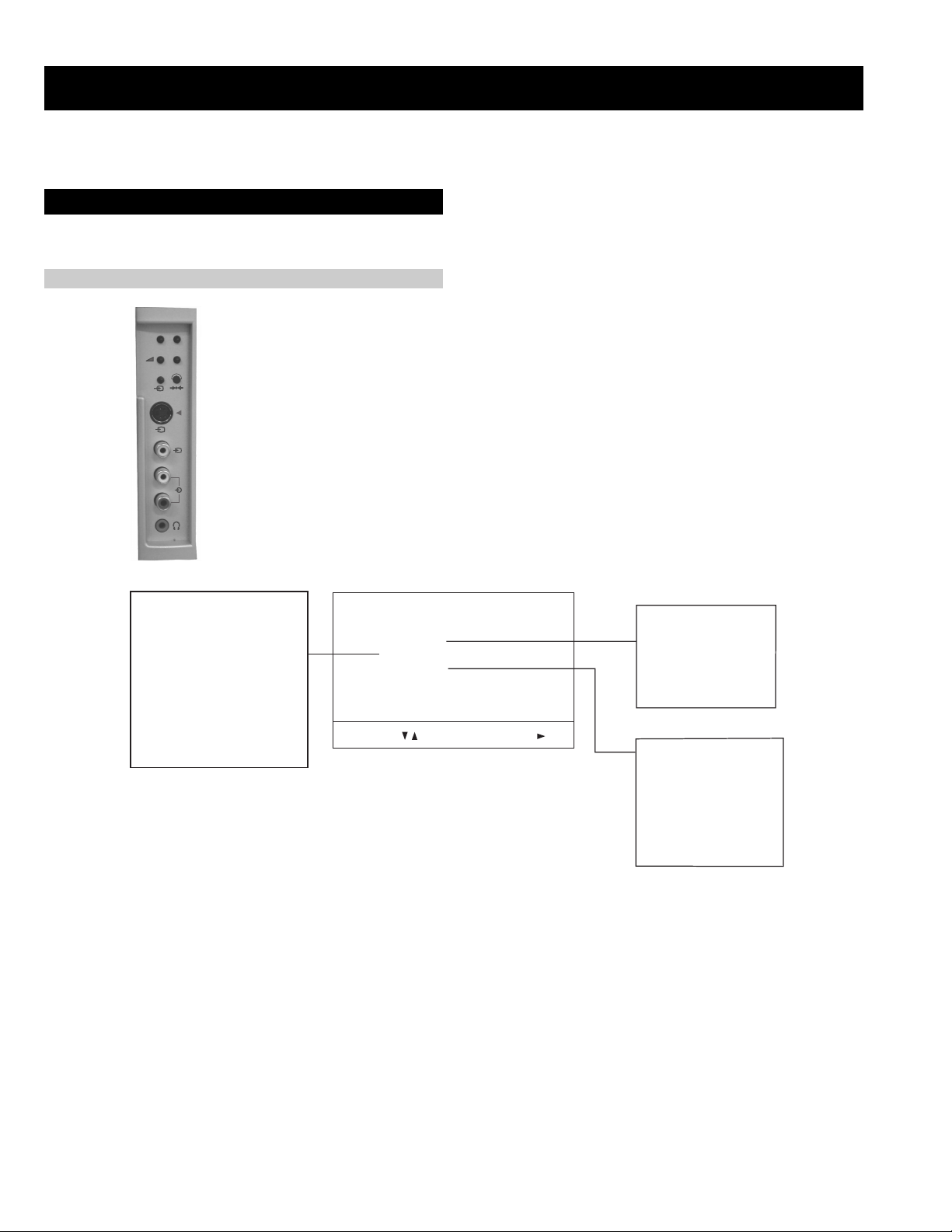
p
- +
1. Turn on the main power switch of the set while pressing P + (plus) and P - (minus) b uttons on the
side pop out control panel.
2. When the picture appears release the P+ and P- buttons.
3. ‘TT’ will appear in the upper right corner of the screen.
4. Press the ‘MENU’ button twice on the remote commander to obtain the service menu on the
screen.
MONO
L/G/S/I
R/D/D/D
s
4
4
4
RESET DEVICES
Backend
Deflection
Ext Deflection
Dynamic Convergence
Colour Decoder 1
Feature Box
Audio/Video Switch
D/A Converter
Sound
SERVICE MENU
Initialising
Reset Devices
Monitoring
Device Register Setting
Special Adjustment
Select :
INITIALISING
Model Setting
Destination Setting
Basic Setting
Feature Setting
Next Menu
MONITORING
Device Status monitor
Error Monitor
Production Monitor
NVM Monitor
Format Monitor
CNI Monitor
4. Push the joystick up or down on the remote commander to select the adjustment item.
5. Push the right button to proceed to the next menu.
6. If the required adjustment item is ‘Deflection’, push the down button to move to ‘Deflection’.
7. Push the joystick to the right to enter into ‘Deflection’.
8. Change the data in order to comply with each standard.
Note :
• Before performing any adjustments ensure that the correct model has been selected in the ‘Model Setting’ menu.
• After carrying out the service adjustments, to prevent the customer accessing the ‘Service Menu’ switch the TV set OFF and then ON.
24
Page 25

Initialising Menu
Basic Setting
gnisilaitinI
gnitteSledoM
gnitteSnoitanitseD
gnitteScisaB
gnitteSerutaeF
:tceleS:unemtxeN
Model Setting
The menu contains a list with all the available models of this software to
set up the TV set in an easy way . The selection of a model is setting data
for its features and hardware resources which cannot be detected by the
automatic power on H/W detection as well as a special model byte to get
an unique model identification for models which cannot be differed by
features and hardware resources (e.g. KV-28FC60 and
KV-28FC60Z)
Before data is set, the user will be asked if he really wants to set a new
model. If the user agrees, automatically the destination setting menu is
shown.
gnitteSledoM
106CF82-VK
2Z06CF82-VK
306CF92-VK
406CF23-VK
5Z06CF23-VK
606CF43-VK
757QF82-VK
857QF92-VK
957QF23-VK
0157QF43-VK
1107SF82-VK
2107SF23-VK
3107SF63-VK
4156XF82-VK
5156XF92-VK
6156XF23-VK
7156QF92-VK
KCALBytimrofnoCoN=
NEERGledoMelbitapmoC=
DERatadllarofytimrofnoC=
eseR
t
T able.4-1
Indication of Model Compatibility.
Black:
If any data does not match to specific model, the model name is
displayed in black.
Green:
All data which is checked by model setting menu concurs to model
except model byte.
Red:
All data which is checked by model setting menu concurs to model
including model byte.
gnittescisaB
oNrcseDniMxaMataD
1G/B.sySFFONONO
2K/D.sySFFONONO
3L.sySFFONOFFO
4)KU(I.sySFFONOFFO
5)LRI(I.sySFFONONO
6noitpo.taNTXT143
7TRC9:61FFONOFFO
8refoow-buSFFONONO
9yb-dnatsotuAFFONONO
01retlif-bmoCFFONOFFO
11tedCYotuAFFONONO
21tedbmocotuAFFONOFFO
31elbaliavA2VAFFONONO
41elbaliavA3VAFFONONO
51elbaliavA4VAFFONONO
61raer&rF3VAFFONOFFO
71epaTMACESFFONOFFO
81etuMdnuoS1VAFFONOFFO
Table.4-2
Feature Setting
gnitteserutaeF
oNrcseDniMxaMataD
1GPEFFONONO
Table.4-3
Device Register Setting
dnekcaB
noitcelfeD
noitcelfeDtxE
ecnegrevnoCcimanyD
1redoceDruoloC
retrevnoCA/D
dnEhgiHerutaeF
hctiwSoediV/oiduA
dnuoS
Table.4-4
Note:
After selecting a model, it may be necessary to reset some devices to get
the correct data. (Treble/Bass Offset of Sound, deflection adjustments,
...)
25
Page 26

hctiwSoediV/oiduA
dnekcaB
oNrcseDfeDniMxaMataD
11TUOVC0070
22TUOVC2072
3WS1DGFFOFFONOFFO
4WS2DGFFOFFONOFFO
51TUOCY0070
62TUOCY1071
7LRTC0OLFFOFFONOFFO
8LRTC1OLFFOFFONOFFO
91TUOA3073
012TUOA3073
11ETUM3TUOAFFOFFONOFFO
21WSDCZNOFFONONO
313TUOA3073
41LEDPUORG5101351
51R/L3TUOA0030
61FLOV3TUOA0070
71CLOV3TUOA3073
Table.4-5
tnemtsujdAlaicepS
oNrcseDniMxaMataD
1levelBGR070
2niaGBGR0138
3leveLtaPBGR070
4niagtaPBGR01351
5wFartxE0552552
6kcehCskhCGPEFFONONO
7hgiHrecilSFFONONO
8ediWWCFFFONONO
9RNgepMFFONOFFO
01retliFhctoNFFONOFFO
oNrcseDfeDniMxaMataD
1no-RNOFFONONO
2no-GNOFFONONO
3no-BNOFFONONO
4loc-DFFOFFONOFFO
5sixa-roloC2032
6tsartnoC0403604
7vuL-timiL3033
8euH2303623
9ruoloC1303613
01leveL-ITC2032
11ssenthgirB1303613
21ammaG3033
31ssenprahS0303603
41evirD-R1403614
51evirD-G1403603
61evirD-B1403632
71edoM-LBA0030
81thgirBbuS1303622
91leveL-MV2031
02ffotuC-R1303613
12revoerP2032
22ffotuC-G1303632
32leveL-CIPD1031
42ffotuC-B1303692
52narT-CD0030
62tnoC-buS70519
72lvL-2BGRL80510
82lbA-P5105151
92oF.prahSNOFFONONO
03W-gnigAFFOFFONOFFO
13B-gnigAFFOFFONOFFO
231tesffo-BC110 5111
331tesffo-RC1105111
432tesffo-BC70517
532tesffo-RC70517
63roloCbuS08-82-
Table.4-7
11petSDLN7-00
21petSDKP51-00
31petSDRC0517
41petSPHS01-0351petSLOC01-0161petSniagPHS5-00
71petSlevelMV3-00
812VACYotuACSTNFFONOFFO
913VACYotuACSTNFFONOFFO
02elbasiDBGRFFONOFFO
12DGnretnIFFONONO
22tuOxiMCY2VAFFONONO
Table.4-6
oNrcseDfeDniMxaMataD
1tniT1303613
2wGN/PFFOFFONOFFO
3DIN/PFFOFFONOFFO
4ruoloCbuS70517
5rtnoCbuS80518
6OFprahS1031
7QEprahS2032
8niaGprahS80518
9veLtuO-Y5303653
01tnioPSB0030
11veLtuO-C5403654
21tseRCD0030
31OFFPB2032
41QFPB1031
51wSretliFFFOFFONOFFO
Table.4-8
1redoceDruoloC
26
Page 27

noitcelfeD.txE
oNrcseDfeDniMxaMataD
1ytiraeniL7210552721
2ertneCH1303613
3parTH1303613
4noitatoR005520
5esahPsucoF7210552721
)tnoc(1redoceDruoloC
dnuoS
oNrcseDfeDniMxaMataD
1leveL.feR0400204
2niag-otuANOFFONONO
3ni-anA0010
4etum-rraCNOFFONONO
5tuokcolCNOFFONONO
6niag-MANOFFONONO
7edompilC 0020
8loV1TRACS970 72197
9loV2TRACS970 72197
01rPTRACS720 72172
11rp-1S2I610 72161
21rp-2S2I610 72161
31rpMF720 72172
41rp-ciNGB350 72135
51rp-ciNL950 72195
61rp-ciNKD350 72135
71rp-ciNI790 72179
81rp-ciNlrI790 72179
91yaceD-CVA2082
02lov-WbuS0721-00
12qerf-WbuS0250402
22ssaPH-WbuSFFOFFONOFFO
32erts-tapS721+01-721
42ffeoC-tapS0080
52sffossaB03-3+0
62sffoelberT03-3+0
72sffonduoL0090
82sffoloV-pH2-5-5+292timiLS-M03+821-721+03
03timiLB-M03-821-721+0313timiLM-S21+821-721+21
23timiLB-S02-821-721+0233timiLM-B21-821-721+2143timiLS-B02+821-721+02
53xaM.rrE040 55204
63niM.rrE810 55281
73sffO.loV06-04-
oNrcseDfeDniMxaMataD
61wSparT-C0010
71parTD-SNOFFONONO
81FPLNOFFONONO
91LD-Y80018
02bmoC-NNOFFONONO
12leSoediV00510
22leSBGR0030
32enotflaHFFOFFONOFFO
421.FFOrC70517
521.FFObC70517
622.FFOrC70517
722.FFObC70517
82qerFDCV3073
92edoMDCV0031
03SNESCFA1031
13MVMFFOFFONOFFO
23jdAY-R-S60516
33jdAY-B-S40514
43FPH/LLEB2032
53OFLLEBFFOFFONOFFO
63PG-S0030
73DISFFOFFONOFFO
83BNE1BGRFFOFFONOFFO
93HP-SH1010
04OITARN/S3033
Table.4-9
oNrcseDfeDniMxaMataD
1egnaR3603636
2tatSV6303671
3tatSH3303613
4LpmaH7303633
5RpmaH6303633
6YpU1303613
7YwoL3303613
8LpuY0303654
9RpuY0303613
01LwolY1303613
11RwolY0303654
21LpUwobM1303613
31RpUwobM2303613
41LwoLwobM2303613
51RwoLwobM2303613
61lrtCProCTFFOFFONOFFO
71niProCpoT1303613
81lrtCProCBFFOFFONOFFO
91niProCtoB3403613
Table.4-10
ecnegrevnoCcimanyD
Table.4-11
Table.4-12
27
Page 28

noitcelfeD
oNrcseDfeDniMxaMataD
1eziS-V1303653
2noitisoP-V1303603
3pmoC-V1030
4raeniL-V70517
5rroC-S70517
6eziS-H1303672
7CD-WEFFOFFONOFFO
82miTbkAFFOFFONOFFO
9pmA-niP1303692
01pmoC-H0030
11nipC-pU1303653
21niP-M2032
31niPC-oL1303643
41muizeparT70516
51noitisoP-H1303652
61wKlbV0030
71woB-CFA70517
81elgnA-CFA705101
91klB-tfeL8303625
02klB-thgiR2103611
12nureerF-V0030
22tcepsA-V7403674
32wS-mooZFFOFFONOFFO
42nacS-UFFOFFONOFFO
52llorcS-V1303613
62miT-bkA0032
72nilV-pU00510
82nilV-oL00510
Table.4-13
V SIZE
V LIN
AFC V BOW
V POS
H POS
H SIZE
H PIN CUSH
H TIL T
H UP COR
Deflection System Adjustment
1. Enter into the service mode and select ‘Deflection’ from the
menu. The ‘Deflection’ adjustment menu will be displayed.
2. Select and adjust each item to obtain the optimum image.
4-2. V olume Electrical Adjustments
Sub Colour Adjustment
1. Input a PAL colour bar signal.
2. Connect an oscilloscope to CN5400 pin 5 located on the C Board.
3. Enter into the ‘Service Mode’.
4. Choose ‘Backend’ from the menu.
5. Adjust ‘Sub Colour’ data so that the right sides of the waveform
are of equal height.
Same Level
B-Out Wav ef orm
AFC V ANGLE
H LOWER COR
28
Page 29

4-3. TEST MODE 2:
Is available by pressing the ‘TEST’ button twice, OSD ‘TT’ appears. The functions described below are av ailable by selecting the two number s. T o
release the ‘T est mode 2’, press 0, 10, 20 ... twice or switch the TV set into Stand-by mode. Pressing the two Local Control bu ttons (+ and -) during
power ON will also switch into ‘TT’ mode.
In ‘TT’ mode, it is possible to remove the Menu from the screen by pressing the Speaker Off button once. Pressing the Speaker OFF button a
second time will cause the Menu to reappear. The function is kept ev en when the menu is not displayed on screen !!.
00
10
20
30
40
50
60
70
80
01
11
21
31
41
51
61
71
81
91
02
12
22
32
42
52
62
72
82
03
13
23
33
43
53
63
73
83
93
04
14
24
34
44
54
64
74
84
94
05
15
25
35
ffoedom'TT'
mumixamerutciP
muminimerutciP
%03otemuloVenohpdaeh/rekaepsteS
%05otemuloVenohpdaeh/rekaepsteS
%56otemuloVenohpdaeh/rekaepsteS
%08otemuloVenohpdaeh/rekaepsteS
edomgniegA
noitidnoCgnippihS
noitcnufoN
tnemtsujdaerutcipbuS
tnemtsujdaruolocbuS
noitaregifnoctesVTdnanoisreverawtfosyalpsiD
noitcnufoN
5+>-0>-5-noitcnuFotuA-noitatoRerutciP
%05levelerutciP
noetumoiduA
noitcnufoN
tnemtsujdassenthgirbbuS
noitcnufoN
sutatsVTyalpsid,sgnittestxetsedulcniAnoitanitseD
sutatsVTyalpsid,sgnittestxetsedulcniLnoitanitseD
sutatsVTyalpsid,sgnittestxetsedulcniEnoitanitseD
sutatsVTyalpsid,sgnittestxetsedulcniUnoitanitseD
sutatsVTyalpsid,sgnittestxetsedulcniDnoitanitseD
sutatsVTyalpsid,sgnittestxetsedulcniBnoitanitseD
sutatsVTyalpsid,sgnittestxetsedulcniKnoitanitseD
sutatsVTyalpsid,sgnittestxetsedulcniRnoitanitseD
noitcnufoN
1tnemtsujdAyrtemoeG
2tnemtsujdAyrtemoeG
rotinomrorrE
noitcnufoN
sutatsVTyalpsiD;9:61><3:4TRC
hctiwsnoitceted32eniL
tset)MV(noitaludoMyticoleV
noitcnufoN
noitcnufoN
noitcnufoN
kcehcedomneercS
yrtemoegesilaitini-eR
noitcnufoN
noitcnufoN
noitcnufoN
rednammocrelaedrofdevreseR
MVNesilaitini-eR
nigrivnonsaMVNteS
nigrivsaMVNteS
noitcnufoN
%09otemulovybloDteS
ylnorekaepstfelnoybloD
ylnorekaepsthgirnoybloD
45
55
65
75
85
95
06
16
26
36
46
56
66
76
86
96
07
17
27
37
47
57
67
77
87
97
08
18
28
38
68
78
88
98
09
19
29
39
49
59
69
79
89
99
noitcnufoN
noitcnufoN
noitcnufoN
noitcnufoN
noitcnufoN
edomecivreS
MVNfonoitacol
noitcnufoN
noitcnufoN
nororreerongI
noitcnufoN
noitcnufoN
noitcnufoN
noitcnufoN
noitcnufoN
noitcnufoN
noitcnufoN
noitcnufoN
noitcnufoN
noitcnufoN
noitcnufoN
noitcaoN
noitcaoN
noitcnufoN
ylnoertnectfelnoybloD
ylnorekaepsdnuorrusnoybloD
edomnoitcudorP
erutcipehtotniMORmorfatadtesererutcipehtypoC
MVNfonoitacolteser
teserotMVNmorfataderutcipjdalautcaehtypoC
sedocrorreteseR
ffosrorreerongI
slebalnoitatslladna5-1tpecxesemmargorpllaraelC
GPErofniPrenroCreppU/pmANIProftnemtsujdA
GPErofdiozeparT/niPrenroCrewoLroftnemtsujdA
gniknalboedivoN
FFF0-FFE0sesserddAMVNteseR
.01niP2VAnolangistsetkniLtramS
niamtupniX-DIMroftnemtsujdaertneclatnoziroH
kcitsyojthgirdnatfelhtiwenodsitnemtsujdA.erutcip
.snottub"KO"ro"VT"ybdesaeler,nottub
teserDIlanosreP
ffokcoLlatneraP
ffo/noetumDSO
ylnopuorgerawtfosrofdevreseR
lennahcdnuorrusniNOretliFssaPwoLybloD
lennahcdnuorrusniFFOretliFssaPwoLybloD
29
Page 30

Memo
30
Page 31

5-1. BLOCK DIAGRAMS (1)
CN7611
1
2
F1 ( )
F7626
AC FILTER FUSE
POWER SUPPLY AND DEFLECTION
S7601
POWER
1
2
1
2
F4 ( )
POWER SWITCH
CN7601CN7633 CN7602
1
2
CN6700
CN6620
CN6700
FOR
CHECK
D ( )
AC IN
1
DGC
DGC
DGC
CHECK
DGC CHECK
AC IN
IC6651
D
1
S
4
C
5
3
2
1
1
2
RELAY
RY601
RELAY
RY602
+4.5V RECT
D6620
T6601
MAIN RECT
D6604
6
7
1
2
3
4
5
17
16
15
14
13
12
10
9
8
+6.5V RECT
D6619
+10.5V RECT
D6616
+135V RECT
D6617
+22V RECT
D6618
T6600 PRT
3 1
POWER MODULE
IC6604
REG OUT
T6651
5
3
4
2
15
1 37
IC6667
IC6654
1 2
+5VREG
Q6667
+5V
OVER CURRENT PROT
OVER VOLTAGE PROT
STANDBY
+5V
IC603
4
+4.5V
+6.5V
+10.5V
+135V
+22V
+135V
AC ON/OFF
CN6101
13
11
9
1
TO A BOARD
CN1602
TO D1 BOARD
CN6601
TO A
BOARD
CN1601
CN6102
CN6600
19
18
17
16
15
13
10
9
7
5
14
A5
B7
A9
B9
B13
A16
B16
B15
A17
B17
A19
B19
A23
A22
B24
B25
A25
B18
B20 HP2
A7 HP1
A24
A14
E/W
AFC PULSE
EX PARA
RGB AFC
HD IN
DYN FOCUS
VMOD
V PROT
V SAW +
V SAW -
HD2 OUT
HD1 OUT
H SAW
IN PIN
L IN
H CENTER
ABL
DF DRIVE
H-OUT DRIVE
Q6801
H-OUT DRIVE
Q6802
+135V
IC6700
V-OUT
1
5
7
V OUT
Q6700
TO A BOARD
CN1700
CN6500
G2
1
TO C BOARD
4
H
HDT
T6801
HDT
T6802
2
+
3
6
-
+
5
IC6801
H-OUT
Q6803,
Q6804
1
7
AMP
Q6809
Q6810
T6805
Q6808
V+
V-
H-
H+
T6804 FBT
Q6805
Q6806
-15V
+15V
+200V
+135V
-15V RECT
D6809
+15V RECT
D6808
+200V RECT
D6805
1
4
2
6
5
7
8
9
10
HV
FV
DFT
T6852
DF DRIVE
Q6851
14
13
11
CN6611
6
5
4
3
2
1
CN5601
DY ASSY
V- DY+
V- DY-
H- DY-
H- DY+
TO PICTURE TUBE
HV
TO C BOARD
FV
V DY
H DY
TO A BOARD
CN1703
TO A BOARD
CN1702
CN7100
CN7103
1
3
7
5
9
11
CN7102
1
3
H8 ( )
RESP
4
3
SIRCS
2
2
+5V STBY
1
RECEIVER
HEADPHONE R IN
HEADPHONE L IN
AV3 CHROMA OUT
AV3 LUMINANCE OUT
AV3 L OUT
AV3 R OUT
KEY 2
KEY 1
LED,
IR RECEIVER
+12V
IC7150
4 3
2 1
S7900
S7901
S7902
H7 (
Y/C
VIDEO
L
R
HEADPHONE
J7900
SIDE AV,
HEADPHONE AND
)
CONTROL SWITCH
J7925
31 32 33
34
Page 32

CN1801
B13
A15
B15
B18
QSS2 OUT
HEADPHONE RIGHT IN
HEADPHONE LEFT IN
AV3 CHROMA OUT
AV3 LUMINANCE OUT
AM 2 OUT
CVBS 2 OUT
AUDIO LEFT
AUDIO SURROUND
AUDIO CENTER
AUDIO RIGHT
HEADPHONE MUTE
AV3 RIGHT OUT
AV3 LEFT OUT
AV LINK I/O
MODE (PIN B)
CVBS IN (TEXT)
AUDIO RESET
H PULSE SUB IN
A19
B19
V PULSE SUB IN
V SUB IN
A20
U SUB IN
B22
H PULSE MAIN IN
A21
Y SUB IN
A23
A24
V PULSE MAIN IN
V MAIN IN
A25
U MAIN IN
B25
Y MAIN IN
B4
MODE (PIN 8)
B5
AV LINK I/O
B9
B8
CVBS IN (TEXT)
AUDIO RESET
B11
TEXT BLANKING IN
B12
BLUE TEXT IN
B14
RED TEXT IN
B13
GREEN TEXT IN
B17
V SYNC TEXT
B18
H SYNC TEXT
A12
STANDBY
A13
PROTECTION
A14
AC ON/OFF
B20
AUDIO MUTE
B3
AGC MONITOR
4
5
11
14
15
16
SCL
SDA
AGC MONITOR
SDA
SCL
AGC
MONITOR
AM1
QSS1
CVBS1
BUFFER
Q1328,
Q1329
BUFFER
Q1326,
Q1327
MUTE SW
Q1201
A3
A2
B1
A5
A4
B4
A6
B6
A7
A8
A13
A11
B11
A12
A1
9
10
1
1
A11
A12
A13
A14
A16
A17
A18
A19
A20
A2
A3
A4
A5
B19
A20
B20
A7
A8
B8
B7
B18
5
17
18
10
19
14
6
16
9
13
7
15
TO E BOARD
CN4101
TO B2 BOARD
CN2100
V SUB OUT
DPIC SW
V-100 IN
Y-100 IN
U-100 IN
V-100 OUT
Y-100 OUT
U-100 OUT
DPIC SW
B5
A4
A5
A2
B2
A3
B3
B1
A11
B11
A1
A6
A10
B10
9
11
1
3
5
7
TO H7 BOARD
CN7904
TO D BOARD
CN6102
TO J BOARD
CN8101
TO M1 BOARD
CN9101
5
9
11
13
TO D BOARD
CN6101
STANDBY
AC ON/OFF
OVER VOLTAGE
OVER CURRENT PROT
IC1400
I/O EXPANDER
AUDIO
PROTECTION
Q1226,1227,
1626
8
6
1
MUTE SW
Q1208
13
11
3
AUDIO CENTER
AUDIO SURROUND
AUDIO LEFT
AUDIO RIGHT
HEADPHONE RIGHT OUT
AV3 CHROMA IN
HEADPHONE LEFT OUT
AV3 LUMINANCE IN
AV3 LEFT OUT
AV3 RIGHT OUT
HORIZONTAL DEFL
RED TEXT OUT
VERTICAL DEFL
GREEN TEXT OUT
TEXT BLANKING OUT
BLUE TEXT OUT
EXTRA PARABOLA
FLYBACK PULSE
HORIZONTAL DRIVE
DYNAMIC FOCUS
EAST/WEST
VERTICAL SAW+
VERTICAL PROTECT
VERTICAL SAW-
RGB AFC
X-RAY
ABL
VM MODULATION
INST+
OUTS
INC+
MUTE
MUTE
OUTC
SURROUND
CENTER
IC1126
AUDIO AMPLIFIER
LEFT
IC1176
AUDIO AMPLIFIER
CENTER AND
SURROUND
IC1126
AUDIO AMPLIFIER
RIGHT
CN1200
CN1401
CN1703
CN1601
CN1602
CN1901
TU1326
INPUT
OUTPUT
STBY/MUTE
STBY/MUTE
OUTPUT
INPUT
10
9
STANDBY
4
1 2
IC1601
+5VREG
+6.5V
+5V
ANALOGUE
4
1 2
IC1602
+5VREG
+5V
DIGITAL
4
1 2
IC1605
+3.5VREG
+4.5V
+3.5V
4
1 2
IC1604
+9VREG
+10.5
+9V
A4
A5
5
4
TO H8 BOARD
CN7150
CN1700
LED
SIRCS
A10
B9
A9
CVBS 1 OUT
AM 1
QSS 1 OUT
16
CVBS2
15
QSS2
14
AM2
5
SDA
4
SCL
BUFFER
Q1328,
Q1329
TU1350
(SUB-TUNER)
RESPONSE LED
SIRCS
V PULSE SUB OUT
4
MID HP
PORT 2
TEXT HP
2
1
IC1401
4
MID VP
PORT 2
TEXT VP
2
1
1
10
OV PROT
AUDIO PROT
OC PROT
9
3
PORT 2
A (
)
SIGNAL AND AUDIO AMP
4
1
1
3
3
1
A3
A2
CN1702
TO H7 BOARD
CN7902
U SUB OUT
Y SUB OUT
Y MAIN OUT
U MAIN OUT
V MAIN OUT
V PULSE MAIN OUT
H PULSE MAIN OUT
5-1. BLOCK DIAGRAMS (2)
TO A BOARD
CN1801
CN8900
AV1
CN8901
AV2
CN8902
A4V
CN8101
(1/2)
7
BLUE IN
11
GREEN IN
15
RED IN
16
BLANKING
1
RIGHT OUT (1)
2
RIGHT IN (2)
3
LEFT OUT (3)
6
LEFT IN (4)
8
MODE (1)
1920VIDEO OUT (2)
VIDEO IN (3)
1
RIGHT OUT (5)
2
RIGHT IN (6)
3
LEFT OUT (7)
6
LEFT IN (8)
10
MODE (2)
10
AV LINK
15
C IN (5)
1920VIDEO OUT (6)
VIDEO IN (9)
1
RIGHT OUT (9)
2
RIGHT IN (10)
3
LEFT OUT (11)
6
LEFT IN (12)
8
MODE 4 (3)
15
C IN AV4 (4)
1920VIDEO OUT
VIDEO IN AV4 (3)
A13
AV LINK
A8
AV3 LUM IN
A7
AV3 C IN
A6
AV3 RIGHT IN
B6
AV3 LEFT IN
B14
SCL
A14
SDA
A10
CVBS1 IN
A15
CVBS OUT (TEXT)
B15
AUDIO RESET
AM1
B9
A9
QSSI IN
AMP
Q8818
MAIN AUDIO/VIDEO SWITCH
32
RTV
36
(R2) AV1-R
25
LTV
29
(L2) AV1-L
18
MODE 1
60
AV1-V (CV IN 2)
40
(R02) AV2-R OUT
35
(R3) AV2-R
41
(L02) AV2-L OUT
28
(L3) AV2-L
19
MODE 2
52
AV2-C(C1)
9
AV2 OUT(CV01)
58
AV2-V(Y1)
33
(R5) AV4-R
26
(L5) AV4-L
20
MODE 3
49
(C3) AV4-C
54
AV4-V(YB)
56
AV3-V(Y2)
51
(C2) AV3-C
34
(R4) AV3-R
27
(L4) AV3-L
6
AD IN
IC8801
IC8700
AUTOWIDE
MAIN Y OUT
MAIN C OUT
(CO2)
SUB C OUT
(YO2)
SUB Y OUT
SDA
SCL
11
13
47
45
SDA
16
SCL
15
IC8500
DIGITAL COMB FILTER
LUMINANCE OUT
6
CLOCK IN
CHROMA OUT
16
15
16
PNR
15
NTPLI
SUB AUDIO/VIDEO SWITCH
11
AV4 C
4
AV4 Y
15
AV3 C
2
AV3 Y
IC8802
Y OUT
C OUT
AMP
Q8300
AMP
Q8302
SCL
SDA
IC8301
MAIN COLOR DECODER
25
B I
26
G I
27
R I
YS 3
15
46
SFC OUT
13
SCL
14
SDA
5
COMB Y
COMB C/
7
FORGED S
45
COMB SYS
Cr OUT
Cb OUT
Y OUT
MAIN L OUT
MAIN R OUT
HPR OUT 3
HPL OUT 3
23
22
21
MAIN L
39
MAIN R
38
HPR
24
HPL
23
AMP
Q8308
AMP
Q8309
AMP
Q8310
HEADPHONE LEFT OUT
HEADPHONE RIGHT OUT
SURROUND SPEAKER (4)
CENTRE SPEAKER (1)
LEFT SPEAKER (3)
RIGHT SPEAKER (2)
1
48
CVBS/YI
CI
CVBS OUT
3
HEADPHONE RIGHT OUT
HEADPHONE LEFT OUT
HP MUTE
IC8401
SUB COLOR DECODER
21
Y OUT
48
CI
1
CVBS/YI
3
13
U OUT
V OUT
22
23
AMP
Q8406
AMP
Q8405
AMP
Q8403
V-M (2)
U-M (1)
Y-M (3)
QSS 2
Y-S (7)
U-S (8)
V-S (9)
AM 2
CN8101
A2
A25
B25
B4
A4
A3
A2
A1
B1
A4
B4
A5
A11
A21
A20
B19
B11
(2/2)
TO A BOARD
CN1801
AUDIO
RESET
QSS1
AM1
BUFFER
Q8200
IC8150
FM DEMULATOR
1
AM IN
3
FM SIF
SDA
SCL
21
POWER ON RESET
67 IF IN1
BUFFER
Q8201
X8200
18.432MHz
RIGHT OUT (9)
LEFT OUT (11)
IC8151
I2C SWITCH
14
SDA
15
SCL
13
SW
3 2
SWODA 4
SCL
SDA
MAIN L
MAIN R
68 IF COMMON IN
IF IN 2
69
60
MONO IN (AM)
XTAL IN
71
XTAL OUT
72
AV MAIN L IN
56
57
AV MAIN R IN
36
TV OUT R
37
TV OUT L
2
SCL
3
SDA
IC8200
SOUND PROCESSOR
SUBWOOFER OUT
IC8101
HP OUT
HP L
6
L IN
HP R
7
R IN
HP MUTE SWITCH
Q8100, Q8101
SURROUND OUT
SPEAKER OUT R
SPEAKER OUT L
CENTER OUT
8
L OUT
1
R OUT
IC8201
OUTPUT AMP
25
27
28
30
24
12
SUR. IN SUR. OUT
10
RIGHT IN RIGHT OUT
5
LEFT IN
3
CENTER IN
CENTER OUT
LEFT OUT
SURROUND SPEAKER (4)
14
RIGHT SPEAKER (2)
8
LEFT SPEAKER (3)
7
CENTER SPEAKER (1)
1
HEADPHONE L OUT
HEADPHONE R OUT
INTERFACE,
J (
AUDIO, CHROMA,
G COMB FILTER
J8901
VARIABLE OUT
L
R
)
35
36 3837
Page 33

U MAIN IN
Y 100
U 100
RESET 100
A20
H-PULSE MAIN IN
A19
V-PULSE MAIN IN
A16
A17
A18
A2
A3
A4
A6
B1
A1
TO A BOARD
CN1200
IC3302
71
51
72
52
54
53
59
60
62
26
61
28
79
76
30
74
66
22
9
68
70
7
20
32
47
24
64
63
VP100
HP100
SWITCH
Q3300
A5
4
5
3
9
35
36
34
37
39
40
38
41
43
44
42
45
21
19
35
36
34
37
39
40
38
41
43
44
42
1
17
16
18
15
13
12
14
11
9
8
10
7
13
12
14
11
9
8
10
7
5
4
6
3
25
37
36
38
35
33
32
34
31
29
28
30
27
17
15
16
24
18
23
26
VM-OUT/MUTE
V 100
V MAIN IN
Y MAIN IN
HRD
PFD-INH
LLD
HRD
PFD-INH
LLD
CN2100
VP50
LLD
P1.1
HRD
HA
BLND
UP-RST
U50IN
V50IN
Y-OUT
U-OUT
V-OUT
WE
SWCK
RSTW
RE
JE2
Y50IN
Y50
U50
V50
Y100
U100
V100
Y0IN
U1IN
U0IN
V1IN
V0IN
Y1IN
Y6IN
Y5IN
Y4IN
Y3IN
Y2IN
Y7IN
VDEF
HDEF
Y3OUT
Y4OUT
Y5OUT
Y6OUT
Y7OUT
U0OUT
U1OUT
Y0OUT
Y1OUT
Y2OUT
V0OUT
V1OUT
IC3303 IC3304
U2
U2
V2
V2
V1
V1
U1
U1
Y1
Y1
Y1
Y1
Y1
Y1
Y1
Y1
V1
V1
U1
U1
Y1
Y1
Y1
Y1
Y1
Y1
Y1
Y1
V3
V3
U3
U3
Y3
Y3
Y3
Y3
Y3
Y3
Y3
Y3
V3
V3
U3
U3
Y3
Y3
Y3
Y3
Y3
Y3
Y3
Y3
Y3OUT
Y4OUT
Y5OUT
Y6OUT
Y7OUT
U0OUT
U1OUT
Y0OUT
Y1OUT
Y2OUT
V0OUT
V1OUT
Y7IN
Y2IN
Y3IN
Y4IN
Y5IN
Y6IN
Y1IN
V0IN
V1IN
U0IN
U1IN
Y0IN
WEIN
VPULSE
YOUT0
UOUT1
UOUT0
VOUT1
VOUT0
YOUT5
YOUT4
YOUT3
YOUT2
YOUT1
YOUT7
YOUT6
YIN7
YIN2
YIN3
YIN4
YIN5
YIN6
YIN1
VIN0
VIN1
UIN0
UIN1
YIN0
RSTR
Y2
Y2
Y2
Y2
Y2
Y2
Y2
Y2
U2
U2
V2
V2
WE
SWCK
RSTN
RE
IE
OE
SRCK
55
56
58
57
Y2
Y2
Y2
Y2
Y2
Y2
Y2
Y2
IC3301
B2 (
)
100 MHz
5-1. BLOCK DIAGRAMS (3)
CN6601
(1/2)
A24
ABL1
A5
E/W
B20
HP2
B13
HDIN
TO D BOARD
CN6600
B3
SCL
A4
SDA2
A7
HP1
A9
EX PARA
B5
VFB
+
5
6
-
-
2
3
+
IC6102
ACTIVE HORIZONTAL SIZE
ADJUSTMENT CONTROL
V PROT
Q6403, Q6404
Q6402, Q6401
CN6622
CY-
3
1
CY+
7
1
HORIZONTAL DRIVE PULSE GENERATOR
HORIZONTAL DRIVE PULSE GENERATOR
HORIZONTAL LINEARITY & INNER PIN CONTROL
+12V
+5V
D/A FOR FOCUS, RO TATI ON , `H ' TR A P
+
2
3
5
6
1
-
-
7
+
IC6100
+
5
6
2
3
7
-
-
1
+
IC6101
+
3
2
6
5
1
-
-
7
+
IC6103
-
6
5
3
2
QP SIGNAL SHAPING
3
2
5
6
IC6351
QP SIGNAL SHAPING
3
4
6
7
ROTATION POWER AMPLIFIER
3
2
5
6
ROTATION PRE-AMPLIFIER
4
P4
7
P7
+
+
-
IC6350
+
-
+
-
+
-
+
-
IC6356
+
-
+
-
IC6355
7
1
1
7
2
8
1
7
5
P5
2
P2
6
P6
IC6302
SWITCH
Q6104
Q6106
SWITCH
Q6104
Q6106
9
VSTST
8
HSTAT
14
HD
17
SCL
16
SDA
MAIN HDY & VDY CONVERGANCE CONTROLLER
REFVOUT
HDYCON
IC6250
VSAW
5
6
3
+
5
6
-
3
+
2
-
IC6352
QP OUTPUT DRIVE STAGE
IC6354
`H' TRAP MULTIPLEXER/SIGNAL
CONDITIONER & `H' LIN
6
8
QP OUT
7
Q6358
1
1
O/P DRIVE STAGE FOR DYNAMIC
+
3
2
-
IC6251
CONVERGNCE
CY AMP
6
Q6253,
6254
D1 (
DEFLECTION
HD2OUT
HD1OUT
IN PIN
VM MOD
DF DRIVE
V PROT
)
CN6601
(2/2)
A23
A22
CN6502
3
TO D BOARD
CN6600
TO VM BOARD
CN6502
B25
L IN
A25
B16
A14
B15
QP-
CN6633
1
3
TO
ROTATION
COIL
39 40 41
42
Page 34

CN4101
B20
B15
B14
B13
B12
A1
A6
A16
B16
A10
B10
B11
A11
A20
A2
B2
B3
B8
A8
13
23
22
1
18
17
43
33
34
35
36
62
61
60
59
58
57
56
55
54
EXTRA PARABOLA
VMID
HDEFL
SDL2
RED
D FOCUS
Y100
U100
V100
SWITCH (PORT 3)
YMID
UMID
VDEFL
SDA2
GREEN
BLUE
BLK
DPIC SW
HD
FB PULSE
EW
ABL
XRAY
Cr2 IN
HS IN
SDL
R2 IN
Cr1 IN
FS
Y2 IN
Ct2 IN
VS IN
SDA
G2 IN
B2 IN
YS/YM2
DPIC DCTR
HD
HP IN
EW
ABL IN
SCP
ABL FIL
B1
A3
B18
B19
53
52
64
63
EXTRA PARA
DF PARA
YIN
Ct1 IN
CN4500
25
26
28
30
1
3
5
8
45
15
2
X4300
503.5 kHz
TO VM BOARD
CN5402
B OUT
G OUT
R OUT
IK IN
VM OUT
500K
CN4502
TO A BOARD
CN1401
IC4301
MULTI COMPONENT PROCESSOR
PICTURE TUBE
CN5400
R
G
TO D BOARD
HV (T6804)
R
G
B
HV
1
3
5
8
IK
B
5
IK
9
VDF
3
VI
1
VB
STANBY SW
Q5351
VOLTAGE DET
Q5375, 5376
+12V
8
VO
IC5350
VIDEO OUT (BLUE)
5
IK
9
VDF
3
VI
1
VB
8
VO
IC5325
VIDEO OUT (GREEN)
5
IK
9
VDF
3
VI
1
VB
8
VO
IC5300
VIDEO OUT (RED)
STANBY SW
Q5325
STANBY SW
Q5300
POWER ON SWITCH
Q5350
+12V
6
7
8
TO D BOARD
FV (T6804)
G4
G2
1
H1
3
H1
4
G2
1
G2
RV5375
CN5600
TO D BOARD
CN6500
FV
J5375
RED
GREEN
BLUE
IK
E (
)
RGB OUT / CHROMA
C (
)
CRT DRIVE
19
L2FJL
5-1. BLOCK DIAGRAMS (4)
TO A BOARD
CN1901
CN9101
B6
B1
B7
A2
A3
B3
A4
B4
A5
A12
A13
A14
A10
A20
B5
B8
B10
A11
B20
B17
B18
B15
B11
B9
B16
B12
B13
B14
SCLO
DISABLE
SDAO
KEY2
KEY1
AGC MONITOR
RESP. LED
PIN8
SIRCS
ST BY
PROT
AC ON/OFF
RST IN
MID BUSY
AV LINK
RES. AUDIO
RESET 100
TC LED
AUDIO MUTE
VP 100
HP 100
TXT CLK
TXT BLK
VIDEO
TCS
TXT B
TXT G
TXT R
SWITCH
Q9108,9109
SWITCH
Q9110
SWITCH
Q9106,9107
IC9108
IC9100
KEY PAD DRIVER
5
+1
3
SWITCH
Q9105
IC9104
TC LED
SWITCH
Q9100
IC9110
PULSE
ENABLE
CLOCK
MTX RES
DSD OFF
12
13
2
1
1
RESET
MASTER RESET I.C.
14
RES. AUDIO
13
RES. PICTURE
12
11
AUDIO MUTE
IC9500
TEXT BLANKING GENERATOR
11
10
9
8
6
OUT2+2
OUT1
DATA
/STR
IC9105
MAIN MICRO-CONTROLLER
5
SDA
6
SCL
7
WP
X9101
16MHZ
7
1
8
7
6
EO
15
3
2
1
6
7
SWITCH
Q9504,9503
AMPLIFIER
Q9500,9501,
9502
43
9
SCLO
87
SCL1
86
SDA1
10
SDA0
95
CS/DISABLE
30
WP
6
XTAL1
7
XTAL2
94
TC INT
KEY2
99
100
KEY1
2
AGC MON
12
RESP LED
91
PIN8
98
SIRCS
13
ST.BY
PROT
92
93
AC ON.OFF
32
WDT CLK
31
WDT EN
78
RST IN
1
MID BUSY
11
AVLINK OUT
90
AV LINK IN
79
/RST OUT
23
CLOCK
15
DATA
14
/STR
3
VP 100
4
HP 100
A(19)
A19
29
A(18)
A18
28
A(17)
27
A17
A(16)
26
A16
A(15)
75
A15
A(14)
74
A14
A(13)
73
A13
A(12)
72
A12
A(11)
71
A11
A(10)
70
A10
A(9)
A9
69
A(8)
68
A8
A(7)
65
A7
A(6)
64
A6
A(5)
63
A5
A(4)
62
A4
A(3)
61
A3
A(2)
60
A2
A(1)
A1
59
A(0)
58
A0
CS0
81
83
CS2
33
/RD
34
/WR
D(16)
AD15
57
D(15)
AD14
56
D(14)
55
AD13
D(13)
54
AD12
D(12)
53
AD11
D(11)
52
AD10
D(10)
51
AD9
D(9)
50
AD8
D(8)
47
AD7
D(7)
46
AD6
D(6)
AD5
45
D(5)
44
AD4
D(4)
43
AD3
D(3)
42
AD2
D(2)
41
AD1
D(1)
40
AD0
16
M3LEN
17
MRST
18
MTSR
22
SCLK
MEGATEXT I.C.
68
67
66
17
RES
VS
4
5
HS
2
CLK
64
BLAN
10
CVBS
3
TCS
GPO
8
63
B
62
G
R
61
IC9502
XOUT
6
XIN
7
X9500
20.480MHZ
CS2
A(14)
A(13)
A(12)
A(11)
A(10)
A(9)
A(8)
A(7)
A(6)
A(5)
A(4)
A(3)
A(2)
A(1)
A(0)
A(19)
A(18)
A(17)
A(16)
A(15)
A(14)
A(13)
A(12)
A(11)
A(10)
CS0
A(9)
A(8)
A(7)
A(6)
A(5)
A(4)
A(3)
A(2)
A(1)
/RD
IC9109
PROGRAMMABLE O.T.P.
A(18)
2
A(17)
3
A(16)
35
36
A(15)
Q15A-1
A(14)
37
A(13)
38
A(12)
39
A(11)
40
A(10)
41
A(9)
42
A(8)
43
4
A(7)
5
A(6)
A(5)
6
A(4)
7
A(3)
8
A(2)
9
A(1)
10
A(0)
11
12
E
14
G
1
RD
6
WR
27
CS
8
A14
5
A13
9
A12
2
A11
28
A10
3
A9
4
A8
10
A7
11
A6
12
A5
13
A4
14
A3
15
A2
16
A1
17
A0
IC9107
R.A.M.
Q14
Q13
Q12
Q11
Q10
Q9
Q8
Q7
Q6
Q5
Q4
Q3
Q2
Q1
Q0
D7
D6
D5
D4
D3
D2
D1
D0
D(15)
32
D(14)
30
D(13)
28
D(12)
26
D(11)
22
D(10)
20
D(9)
18
D(8)
16
D(7)
31
D(6)
29
D(5)
27
D(4)
25
D(3)
21
D(2)
19
D(1)
17
D(0)
15
D(7)
26
D(6)
25
D(5)
24
D(4)
23
D(3)
22
D(2)
20
D(1)
19
D(0)
18
A(18)
A(17)
A(16)
A(15)
A(14)
A(13)
A(12)
A(11)
A(10)
A(9)
A(8)
A(7)
A(6)
A(5)
A(4)
A(3)
A(2)
A(1)
A(0)
9
A18
A17
6
10
A16
11
A15
5
A14
4
A13
12
A12
1
A11
31
A10
2
A9
3
A8
13
A7
14
A6
15
A5
16
A4
17
A3
18
A2
A1
19
20
A0
IC9400
WR
RD
D7
D6
D5
D4
D3
D2
D1
D0
7
32
D(7)
29
D(6)
28
D(5)
27
D(4)
26
D(3)
25
D(2)
23
D(1)
22
D(0)
21
M1 (
MICRO TEXT
)
VELOCITY MODULATION
(
VM AMP
Q5400,5401
)
VM BUFFER
Q5402,5403,
5404,5405
VM OUT
Q5406,5407
Q.P -
Q.P +
1
2
3
4
7
8
CN5444
TO
D1 BOARD
CN6502
TO E BOARD
CN4502
CN5602
CN5402
3
4
2
VM
Q.P -
Q.P +
VM IN
44 4645
QP-
QP+
VM
NECK
ASSY
5-2. CIRCUIT BOARD LOCATION
C
C Board
VM Board
VM
CVM Board
H
H7 Board
D1
H8 Board
D Board
F4 Board
D1 Board
E Board
M1 Board
J Board
A Board
5-3. SCHEMATIC DIAGRAMS AND
PRINTED WIRING BOARDS
Note :
• All capacitors are in µF unless otherwise noted.
• pF : µµF 50WV or less are not indicated except for
electrolytic types.
• Indication of resistance, which does not have one for
rating electrical power, is as follows.
Pitch : 5mm
Electrical power rating : 1/4W
• Chip resistors are 1/10W
• All resistors are in ohms.
k = 1000 ohms, M = 1000,000 ohms
• : nonflammable resistor.
• : fusible resistor.
• : internal component.
• : panel designation or adjustment for repair.
• All variable and adjustable resistors have
characteristic curve B, unless otherwise noted.
• All voltages are in Volts.
• Readings are taken with a 10Mohm digital mutimeter.
• Readings are taken with a color bar input signal.
• Voltage variations may be noted due to normal production
tolerences.
•: B + bus.
• : B - bus.
• : RF signal path.
• : earth - ground.
• : earth - chassis.
F1 Board
D
S1 Board
D2
N
B2 Board
A
J
A2
A Board
A1
Reference Information
RESISTOR RN
RC
FPRD
FUSE
RS
RB
RW
COIL LF-8L
CAPACITOR TA
PS
PP
PT
MPS
MPP
ALB
ALT
ALR
Note :
The components identified by shading
and marked are critical for safety.
Replace only with the part numbers
specified in the parts list.
Note :
Les composants identifiés par une trame et
par une marque sont d'une importance
critique pour la sécurité. Ne les remplacer
que par des pièces de numéro spécifié.
specified.
: METAL FILM
: SOLID
: NON FLAMMABLE CARBON
: NON FLAMMABLE FUSIBLE
: NON FLAMMABLE METAL OXIDE
: NON FLAMMABLE CEMENT
: NON FLAMMABLE WIREWOUND
: ADJUSTMENT RESISTOR
: MICRO INDUCTOR
: TANTALUM
: STYROL
: POLYPROPYLENE
: MYLAR
: METALIZED POLYESTER
: METALIZED POLYPROPYLENE
: BIPOLAR
: HIGH TEMPERATURE
: HIGH RIPPLE
Page 35

H7[ FRONT AV, S-VIDEO ]
F4[ PO WER SWITCH ]
F4[ PRINTED WIRING BOARD ]
H7[ PRINTED WIRING BOARD ]
F1[ A C FILTER FUSE ]
H8[ PRINTED WIRING BOARD ]H8[ IR RECEIVER FOR SIRCS AND LED ]
F1[ PRINTED WIRING BOARD ]
47
48
Page 36

E [ R, G, B OUT CHROMA ]
5049
Page 37

E [PRINTED WIRING BOARD (A side)]
E [PRINTED WIRING BOARD (B side)]
51
Page 38

M1 [ PRINTED WIRING BOARD (A side) ] M1 [ PRINTED WIRING BOARD (B side) ]
52
Page 39

123 4 5 6 7 8 9 1011121314151617181920
A
B
C
D
E
21
F
G
H
I
J
K
L
M
N
O
P
Q
R
S
T
M1[ MICROPROCESSOR AND TEXT DECODER ]
555453
Page 40

19 182021
17 16 15 14 13 12 11 10 9 8 7 6 5 4 3 2 1
A
B
C
D
E
F
G
H
I
J
K
L
M
N
O
P
Q
D1[ DEFLECTION ]
56 57
R
S
58
Page 41

ABCDEF
1
2
3
G
H
4
5
CI
0016CI2-G2536CI5-A3016Q3-G8116Q5-G9216Q3-G3536Q3-B5546Q3-F8216D3-D5536D4-C
1016CI2-H3536CI4-D4016Q3-F9116Q4-G1026Q4-G4536Q2-B5646Q2-D9216D3-F8536D2-B
2016CI3-G4536CI2-D5016Q2-G0216Q4-G2026Q4-G6536Q5-B
3016CI5-H5536CI1-D6016Q2-F2216Q4-G0526Q4-F8536Q2-B2016D3-G5526D2-D1046D4-E
0526CI3-F6536CI1-E7016Q2-H3216Q3-H1526Q4-E1046Q5-D4016D4-G0536D4-C2046D4-E
1526CI2-D
2036CI3-D0016Q3-G0116Q2-F6216Q5-H0536Q4-C3046Q4-D7016D4-H2536D3-A4046D1-C
0536CI3-B1016Q2-G2116Q3-H7216Q3-D1536Q5-B4046Q5-D8016D4-H3536D2-B5046D1-D
1536CI5-B2016Q3-H3116Q4-H8216Q4-H2536Q3-C5046Q1-C7216D3-D4536D3-A
EDOID
ROTSISNART
8016Q2-G5216Q5-H2526Q2-E2046Q5-E5016D3-G1536D5-C3046D1-D
3526D2-F9536D1-C
D1[ PRINTED WIRING BO ARD ]
59
60
Page 42

ABCDEF
1
2
3
G
HIJKLM
D board Waveforms
TP1 TP2
570 mVp-p (V) 58 Vp-p (V)
TP3
2.28 Vp-p (H)
TP5 TP6
5ms/div
10us/div 10us/div
TP4
TP4
131 Vp-p (H)
10us/div 10us/div
5ms/div
oNfeR
0066CI
0076CI
1086CI
elbaTegatloVCI
oNniP )V(egatloV
17.431
25.2
31.9
40
14.1
32.21-
58.0-
60.51
74.1
10
20
30
52.2
67.6
71.0
4
5
6
7
8
9
2.14 Vp-p (H) 150 Vp-p (H)
10us/div 20us/div
TP7
1.07 kVp-p (H)
TP9
TP8
2.3 Vp-p (H)
10us/div 10us/div
TP10
1.72 kVp-p (H) 265 Vp-p (H)
TP11
5ms/div 5ms/div
TP12
1.98 Vp-p (V) 116 Vp-p (V)
Semiconductor Voltage Table
feR )e( )b( )c( feR )e( )b( )c(
6766Q8.15.25 3066Q008.11
7766Q8.11.25 5066Q07.00
8766Q8.16.15 8066Q005.3
7086Q04.60 1866Q04.110
1086Q03.0167066Q3.05.05
2086Q04.0-7.371586Q01-6.48
3086Q02.5310
4086Q006.5315086Q0222
2066Q1.98.110 6086Q04.17.531
feR )s( )g( )d(
10
D [ PRINTED WIRING BOARD ]
CI
0066CI6-I7666CI5-N0066Q01-G8066Q2-L7766Q4-N1086Q8-B7086Q2-M3066D4-L6166D4-I2266D3-M8266D1-N3566D8-M6766D3-M5086D8-C1186D4-D
4066CI8-K6766CI5-M2066Q7-I1166Q1-M8766Q4-M2086Q5-F1586Q9-B4066D9-K7166D4-H3266D5-H9266D3-L4566D7-M7766D3-M6086D8-C1586D8-B
1566CI7-M0076CI4-F3066Q7-H1566Q5-M9766Q3-M3086Q6-B
2566CI1-G1086CI1-C5066Q4-L2566Q5-N0866Q3-M4086Q4-E0066D01-G0166D3-M9166D3-H5266D2-M1366D01-F6566D5-M9766D4-M8086D7-H
3566CI1-I6066Q1-M7666Q5-M1866Q4-M5086Q4-D1066D01-G3166D4-M0266D3-I6266D2-M1566D8-M8566D8-M1866D5-M9086D2-M
4566CI5-L
7066Q5-I6766Q4-M0076Q3-G6086Q4-C2066D01-F5166D3-M1266D2-L7266D1-J2566D8-M9566D6-M1076D3-G0186D4-D
SROTSISNART
EDOID
5066D5-M8166D2-K4266D2-M0366D2-L5566D7-M8766D3-M7086D7-G2586D8-B
6261
NOTE:
Portions of the circuit marked as shown are high
voltage areas. Use care to prevent electric shock
during inspection or repair.
Page 43

123 4 5 6 7 8 9 1011121314151617181920
A
B
C
D
E
21
F
G
H
I
J
K
L
M
N
O
P
Q
R
S
T
D [ POWER SUPPLY AND DEFLECTION ]
656463
Page 44

19 182021
17 16 15 14 13 12 11 10 9 8 7 6 5 4 3 2 1
A
B
C
D
E
F
G
H
I
J
K
L
M
N
O
P
Q
A [ SIGNAL AND AUDIO AMPLIFIER ]
R
S
66 67 68
Page 45

123 4 5 6 7 8 9 1011121314151617181920
elbaTegatloVCI
oNfeR
oNniP )V(egatloV
6211CI
10
211-
301
691-
90
011.4
2111-
1511CI
10
211-
301
681-
90
011.4
2111-
0041CI
10
36.4
56.4
60.4
90
010
415.4
515.4
6711CI
10
33
63
70
80
90
113
210
310
410
feR )e( )b( )c( feR )e( )b( )c(
0011Q5.016.010 9221Q59.40
1011Q002.26231Q2.18.14.4
1021Q06.00 7231Q54.47.1
2021Q01.01.28231Q6.22.33.8
0031Q06.40 9231Q53.85.4
6221Q009.41061Q005
7221Q009.42061Q9.33.30
CI
3041Q9-L
6211CI7-G4041Q9-L
1511CI7-I5041Q8-M
6711CI41-K6041Q9-M
0041CI01-E1061Q11-B
1061CI4-L2061Q9-C
4061CI5-L6261Q9-F
5061CI7-L
EDOID
2-I0361CI1011D9-B
2-L1361CI1011D9-B
ROTSISNART
2011D9-B
0011Q9-B3011D01-D
1011Q9-C4011D41-E
1021Q21-F1021D31-K
2021Q21-F1041D21-E
4021Q21-F2041D21-E
6221Q51-J5041D11-L
7221Q51-J6041D11-L
9221Q41-I7041D11-L
0031Q31-G8041D11-L
6231Q21-L1061D9-C
7231Q21-L2061D9-C
8231Q31-K6261D21-B
9231Q31-K7261D01-F
1041Q9-L0361D1-H
2041Q9-L1361D3-L
ABCDE F
G
HI JKLMN
1
2
3
4
5
6
7
8
9
10
11
13
14
12
21
A
B
IC Voltage Table
C
D
E
F
G
H
I
Semiconductor Location Table
J
K
L
M
N
O
P
Q
R
S
T
Semiconductor Voltage Table
A [ PRINTED WIRING BOARD ]
717069
Page 46

19 182021
CI
0518Q5-A5048Q3-G0188D4-G
1018CI5-B1518Q5-A6048Q2-G1188D9-D
0518CI5-B2518Q5-A1058Q6-F2188D8-D
1518CI4-A3518Q5-A1098Q1-D3188D4-G
0028CI3-J4518Q4-A
EDOID
4188D4-G
1028CI4-J6518Q4-B0518D5-A0098D3-A
2028CI3-I7518Q4-C1518D5-A1098D8-J
1038CI2-F0028Q3-J2518D5-A2098D3-A
2038CI1-F1028Q4-J3518D4-I3098D3-A
1048CI2-I2028Q4-I0028D8-B4098D7-J
2048CI2-H0038Q1-D1028D8-B5098D7-J
0058CI2-E2038Q1-E2028D9-H6098D7-I
0558CI1-G3038Q2-F3028D8-H7098D8-I
1068CI4-I5038Q1-E1088D8-E8098D8-I
2068CI1-H6038Q1-F2088D4-F9098D7-I
3068CI1-I8038Q3-E3088D3-G0198D7-I
4068CI1-I9038Q1-F4088D9-D1198D7-I
0078CI1-C0138Q2-E5088D8-D2198D3-D
1088CI4-F1048Q2-H6088D8-D3198D7-H
ROTSISNART
2048Q7-C7088D8-D4198D7-H
0018Q9-G3048Q3-H8088D8-D5198D7-H
1018Q9-F4048Q2-G9088D3-G
feR )e( )b( )c( feR )e( )b( )c(
0518Q9.26.30.52038Q0.16.10.9
1518Q04.08.43038Q3.19.17.7
2518Q06.40 5038Q3.19.13.7
3518Q04.08.46038Q1.01.00.5
4518Q06.40 1048Q1.01.00.5
6518Q9.36.40.94048Q2.19.14.7
7518Q9.36.40.99088Q7.21.20
0028Q9.15.20.57188Q9.36.40.9
1028Q2.19.10.51098Q9.15.20.9
2028Q1.58.50.9
feR )s( )g( )d(
0038Q6.10.10 5188Q8.106.0
elbaTegatloVCI
oNfeR
oNniP )V(egatloV
oNfeR
oNniP )V(egatloV
0028CI
3-27.4
0058CI
2-15.1
6-45.235.0
76.066.2
717.079.0
120.590.1
638.3118.2
737.331-218.1
830.7410.1
040.732-220.5
547.3620.5
75-658.3030.5
856.2734.2
068.324-049.1
764.0449.1
96-865.1
1018CI
12.4
174.231.4
272.256.0
1028CI
3-10.585.0
01-50.5
1088CI
18.1
41-210.54-25.4
1038CI
14.250
29.17-66.4
35.180
41.096.4
54.2014.3
76.2118.3
93.0315.4
018.003-225.4
115.214-235.4
41-315.4346.4
024.2547.3
128.1645.3
32-229.1745.4
421.0945.4
72-525.208-155.4
928.2
1518CI
24.2
731.136.4
830.446.4
1048CI
13.254.0
29.166.4
41.074.0
93.090
010.4016.2
114.2
0518CI
10.3
024.225.2
127.137.1
32-229.163.4
731.1214.2
830.4316.4
043.3415.2
748.3
848.1
ABCDE F
G
HI J
1
2
3
4
5
6
7
8
9
10
17 16 15 14 13 12 11 10 9 8 7 6 5 4 3 2 1
A
B
Semiconductor Location Table
IC Voltage Table
C
D
E
F
G
H
J [ PRINTED WIRING BOARD ]
I
J
K
Semiconductor Voltage Table
L
M
N
O
P
Q
R
S
72 73 74
Page 47

123 4 5 6 7 8 9 1011121314151617181920
A
B
C
D
E
21
F
G
H
I
J
K
L
M
N
O
P
Q
R
S
T
75 76
J [ INTERFACE, AUDIO, CHROMA (Page 1/2) ]
77
Page 48

19 182021
17 16 15 14 13 12 11 10 9 8 7 6 5 4 3 2 1
A
B
C
D
E
F
G
H
I
J
K
L
M
N
O
P
Q
J [ INTERFACE, AUDIO, CHROMA (Page 2/2) ]
R
S
807978
Page 49

feR)e()b()c(feR)e()b()c(
1035Q5.38.20 0035Q7.34.48.3
6235Q6.330 5235Q7.34.48.3
2535Q7.330 1535Q8.34.49.3
5735Q3.019.01110535Q119.019.3
6735Q113.019.01
elbaTegatloVCI
oNfeR
oNniP )V(egatloV
19.3
38.3
54.8
0035CI
70.351
80.751
90.251
19.3
38.3
57.8
5235CI
70.051
80.551
90.051
19.3
38.3
54.8
0535CI
70.051
80.651
90.941
C board Waveforms
TP1 TP2
117 Vp-p (H) 109 Vp-p (H)
TP3
109 Vp-p (H)
TP5 TP6
2.5 Vp-p (H) 2.5 Vp-p (H)
TP7
5us/div
10us/div 10us/div
TP4
TP4
10us/div 5us/div
10us/div
10us/div
2.5 Vp-p (H)
81
3.64 Vp-p (H)
C [ PRINTED WIRING BOARD ]
82
Page 50

feR )e( )b( )c(
0045Q9.05.10.9
1045Q0.16.12.5
2045Q0.66.60.9
3045Q9.50.60.9
4045Q2.59.50
5045Q9.58.50
6045Q1.5316.4312.86
7045Q8.04.12.86
8045Q6.79.64.1
9045Q9.65.70.9
VM board Waveforms
TP1 TP2 TP3
117 Vp-p (V) 109 Vp-p (V) 109 Vp-p (V)
10us/div 10us/div 20us/div
VM[ PRINTED WIRING BOARD ]
83
B2[ PRINTED WIRING BOARD [A] SIDE ]
B2[ PRINTED WIRING BOARD [B] SIDE ]
84
Page 51

123 4 5 6 7 8 9 1011121314151617181920
A
B
C
D
E
21
F
G
H
I
J
K
L
M
N
O
P
Q
R
S
T
B2[ 100Hz PROCESSOR ]
878685
Page 52

19 182021
17 16 15 14 13 12 11 10 9 8 7 6 5 4 3 2 1
A
B
C
D
E
5-5. IC BLOCK DIAGRAMS
D BOARD IC6700 STV 9379 J BOARD IC8101 TDA2822D
2 6 3
FLYBACK
GENERATOR
1
7
-
POWER
AMPLIFIER
+
THERMAL
PROTECTION
4
E BOARD IC4301 CXA2100Q-TL
56 48
S
53
SEP
VIDEO
55
SW
57
59
20
2
9
I REF
51 50 49
SUB
CONT
APC
VCO
TRAP
ACC
ACC
DET
PAL/
NTSC
HUE
PAL
DL
ID
DEM
AXIS
TOT
SHARP
NESS
KILLER
DET
fsc
ID
J BOARD IC8200 MSP3410D-QA-B4
2
5
2
3
2
8
3
1
30
3
4
3
3
37
36
5
54 52 45 46 47
H SYNC
SEP
V SYNC
SEP
DC
D PIC
TRAN
CLP
DEM
DEMODULATOR
Y/C
MIX
COLOR
&AXIS
6
6
5
SBUS Interface I2C Interface
DENT
A/D
A/D
13
8
GATE
50/60 ID
INTER-
LACE
YS
YS/YM
SW
CLP
DFP
SCART Switching Facilities
40 41 39
32fH
VCO
PHASE
DET
1/32
Count Down
GATE
SW
CLP
525/625
OSD
PIC
MIX
DIG
7 645
D/A
D/A
D/A
D/A
D/A
D/A
7
8
6
5
PHASE
PHASE
SHIFT
D-
COL
y
38
DET
SAND
CASTLE
BRT
ABL
2
4
HV
COMP
5
6
5
7
5
9
6
0
4
7
4
8
5
0
5
1
GB
DRV
H.DRIVE
21141387654343
1
3
WIDE
Sawtooth
Gen.
WIDE
Parabola
Gen.
CUT
OFF
AKB
F
G
5-4 SEMICONDUCTORS
U2860B-BFPG3
74LVC08D
14 8
BA7046F
BA7046F-T1
LM393PS-E20
MB3793-42NF
KA78R05TU
KA78R09TU
KA78R33TU
MSP3410D-QA-B4
SAA7185WP
SDA5273P-C134-GEG
SDA5275
STV9379
TDA9320H-N1-518
51
52
33
32
MB3793-42NF-ER
NJM2240M
NJM2240M(TE2)
NJM3404AD
85
1
4
( TOP VIEW )
1
2
3
1 : V IN
2 : V OUT
3 : GND
4 : ON/OFF CONTROL
CAD005AD
LM358
4
9
10
18
26
M27C800-100K1
LM393N
M5216P
M24C32-BN6
CXA1855Q-T6
36
44
42
37
10
30
34
35
32
31
33
37
48
36
1
( TOP VIEW )
25
24
13
12
ST24C16FB6
TDA2822M
UPC393C
7
6
8
2
3
1
LM78L05ACZ
LM78L12ACZ
L78L05ACZ-AP
5
4
640144
7
17
18 28
MSM65355GS
SAB-C161R1-LM
L78L12ACZ-AP
22
24
BLK
26
27
2523282919181716151211164616260
CXA1875AM-T4
HE4094BT
MC14052BDR2
MC74F157ADR2
SN74LS221D
74HCT4046AD/S470
16 9
IN
OUT
GND
SBX1981-51
MB3793-42PNF-ER
1
( TOP VIEW )
8
SDA9361
CXD2053S
TDA4780/V3
28 15
1
( TOP VIEW )
14
MB88141PF-ER
( TOP VIEW )
1
24
34
12
44
13
1
( TOP VIEW )
( TOP VIEW )
1
68
61
60
52
44
433527
1
TC4S69F
5
7
4
64
1
(TOP VIEW)
TEA6422DT
20
19
1
( TOP VIEW )
7
BC546B
BC556B
C 5
1
39
TC55257DFTL-70V-EL
29
TDA6111Q/N4
19
TDA7309D013TR
20
1
( TOP VIEW )
SDA9288X-B121
2333
TDA9143/N2
TDA9144/N2
22
TDA9170T
MSM534031E3Y-Z
12
11
32
1
( TOP VIEW )
3
2
30
11
10
17
16
IN
TLC2933
1
7
TLC5733A
64
1
16
17
TOP209P
85
14
( TOP VIEW )
GND
( TOP VIEW )
OUT
S
G
D
IMZ1A-T109
4
5
6
14
8
3
2
1
6
5
4
1
3
2
IRF614
IRF620
49
48
33
32
DTA144EK
DTA144EK-T146
DTC114EK
DTC114YKA-T146
DTC123EK
DTC123EK-T146
B
E
C
DTC144EK
DTC144EK-T146
2SA1037K-T-146-R
2SA1162-G
2SC2412K-QR
2SC2412K-T-146-R
DTC124EKA-T146
C
E
B
DTA144ESA
DTA144ESA-TP
DTC114ESA-TP
DTC144ESA-TP
2SA1175-HFE
2SA733-K
2SA1837
2SC2500-B
2SC2551-O
2SC2551O-TPE2
2SC2688-LK
2SC3840K
2SC3997CA
MARKING SIDE VIEW
B
C
E
B
C
E
E
B
C
E
B
C
2SA933AS-RT
2SA933AS-QRT
2SA933S-RT
2SC1740S-RT
2SC2785-HFE
B
C
E
2SC4793
B
2SD2396H
B
DAN202K
DAN202K-T-146
3
2
DAP202K
DAP202K-T-146
3
2
DA204K
DA204K-T-146
3
2
H
I
J
C
E
K
L
C
E
M
N
1
2
3
1
O
P
1
2
Q
1
3
R
S
1
2
3
1
88 107
89 90
Page 53

D1NL20-TA
D1NL20U-TR
D1NS4-TR
EGP20G
EL1Z
GP08D
GP08DPKG23
R2K-V1
D10SC4M-F
D10SC6M
RGP02-20EG23
RGP10GPKG23
RGP15GPKG23
S2LA20F
1SS133T-77
1SS83
1SS83TD
CATHODE
ANODE
ERC04-06SE
ERD08M-15
MA73-TX
CATHODE
ANODE
1SS355TE-17
RD12SB2
UDZ-TE-17-3.9B
UDZ-TE-17-4.7B
UDZS-TE-17-5.6B
UDZ-TE-17-6.2B
UDZ-TE-17-6.8B
UDZ-TE-17-8.2B
UDZ-TE-12B
1
1
D4SB60L
D4SB60L-F
RBA-402L
ERA15
ERA38-06TP1
ERA82-004TP1
GP08DPKG23
MTZJ-T-77-13B
MTZJ-T-77-15
MTZJ-T-77-2.2A
MTZJ-T-77-3-3B
MTZJ-T-77-3.6A
MTZJ-T-77-4.7B
MTZJ-T-77-5.6B
MTZJ-T-77-6.8
3
2
3
2
MTZJ-T-77-7.5B
MTZJ-T-77-9.1
MTZJ-T-77-12
MTZJ-T-77-22
MTZJ-T-77-18B
MTZJ-33C
RD5.6ESB2
RD9.1ESB2
PGKE200AG23
1SS119-25
1SS119-25TD
CATHODE
ANODE
ESAC39M-06C
ESAC39M-06CF38
1
2
1
2
MA3033-L
MA3033L-TX
MA3056M-TX
MA3062M-TX
MA3030-H-(TX)
3
2
NC
23
MA3051L-TX
ANODE
CATHODE
UF4005PKG23
ANODE
CATHODE
3
3
1
1
CATHODE
ANODE
CATHODE
ANODE
91
Page 54

NOTE :
• Items with no part number and no description are not
stocked because they are seldom required for routine
service.
• T he construction pa rts of an assembled par t are indicated with a collation number in the rem arks column.
6-1. CHASSIS
22
23
SECTION 6
EXPLODED VIEWS
• Items marked “ * “ are not stocked
since they are seldom required for
routine service. Some delay should
be anticipated when ordering
these items.
28
27
24
26
25
21
17
16
15
14
13
12
11
10
18
9
19
20
21
6
8
7
5
2
3
4
1
REF. NO. PART.NO DESCRIPTION REMARK REF. NO. PART.NO DESCRIPTION REMARK
1 *A-1646-218-A H7 BOARD, COMPLETE
2 *4-205-724-01 F4 BRACKET
3 *A-1646-217-A H8 BOARD, COMPLETE
4 £ 1-571-433-21 SWITCH, PUSH (AC POWER)
5 *A-1624-089-A F4 BOARD, COMPLETE
6 *4-205-196-02 MAIN BRACKET
7 *A-1640-398-A D BOARD, COMPLETE
8 £ 1-453-340-11 TRANSFORMER ASSY, FLYBACK (NX4522//U214)
9 *4-204-476-04 BRACKET, J1
10 *A-1651-137-A J BOARD, COMPLETE
11 *A-1640-380-A D1 BOARD, COMPLETE
12 *A-1640-381-A E BOARD, COMPLETE
13 *A-1620-132-A B2 BOARD, COMPLETE
14 *4-204-477-04 BRACKET, J2
15 1-790-082-11 CABLE, RF
16 £ 1-792-389-11 CORD, POWER
17 1-693-340-11 TUNER/VIF(FR) (KV-29FX65B)
1-693-338-11 TUNER/VIF(AEP) (KV-29FX65E/29FX65K)
18 *A-1624-086-A F1 BOARD, COMPLETE
19 *A-1634-057-A M1 BOARD, COMPLETE
20 *A-1632-913-A A BOARD, COMPLETE (KV-29FX65B)
*A-1632-912-A A BOARD, COMPLETE (KV-29FX65E/29FX65K)
21 1-529-899-11 SPEAKER (24X4.2CM)
22 *A-1678-191-A WOOFER ASSY (SP) 23-26
23 *4-204-775-01 BAFFLE, WOOFER
24 7-685-663-71 SCREW +BVTP 4X16 TYPE 2 IT-3
25 1-529-417-11 SPEAKER (8CM)
26 *4-204-776-01 BOX, WOOFER
27 4-205-721-01 REAR COVER
28 7-685-663-79 SCREW +BVTP 4X16 TYPE 2 IT-3
92
Page 55

6-2. PICTURE TU BE
74
75
76
77
78
59
58
57
73
60
72
71
69
68
70
68
67
66
65
64
63
62
61
56
55
51
52
54
53
REF. NO. PART.NO DESCRIPTION REMARK REF. NO. PART.NO DESCRIPTION REMARK
51 X-4200-636-1 BEZNET ASSY 52-59
52 4-205-720-01 POWER BUTTON
53 4-204-426-01 SPRING
54 4-205-726-01 GUIDE, LIGHT
55 3-022-410-01 DAMPER
56 4-205-722-01 DOOR
57 4-047-464-01 CATCHER, PUSH
58 4-205-725-01 DOOR SPRING
59 4-205-723-01 DOOR BRACKET
60 4-204-058-31 SHEET, BLOTTING
61 £ 8-451-504-31 DEFLECTION YOKE (Y29RSC-S)
62 1-452-896-11 COIL, NA ROTATION (RT200)
63 £ 8-453-011-11 NECK ASSY, (NA299-M)
64 *A-1644-108-A VM BOARD, COMPLETE
65 *A-1638-139-A C BOARD, COMPLETE
66 4-369-318-21 SPRING, TENSION
67 £ 1-416-654-11 COIL, DEMAGNETIC
68 4-203-390-11 CUSHION, DGC
69 *4-204-768-01 HOLDER, DGC (29”)
70 £ 1-251-807-22 CAP ASSY, HIGH-VOLTAGE
71 3-704-495-01 SPACER, DY
72 £ 8-735-053-05 PICTURE TUBE (M68LNH060X)
73 4-046-765-12 SCREW, TAPPING 7+CROWN WASHER
74 4-308-870-00 CLIP, LEAD WIRE
75 1-452-094-00 MAGNET, ROTATABLE DISK; 15MM
76 1-452-032-00 MAGNET, DISK; 10MM
77 X-4387-214-1 PERMALLOY ASSY, CORRECTION
78 3-701-007-00 BAND, BINDING
93
Page 56

SECTION 7
ELECTRICAL PARTS LIST
PARTS LISTING TABLE OF CONTENTS
Page
F4 BOARD COMPLETE Parts List : ........................................................................................................ 95
H8 BOARD COMPLETE Parts List : ........................................................................................................ 95
H7 BOARD COMPLETE Parts List : ........................................................................................................ 95
B2 BOARD COMPLETE Parts List : ........................................................................................................ 95
F1 BOARD COMPLETE Parts List : ........................................................................................................ 97
A BOARD COMMON Parts List : Parts common to all models listed in this manual ......................................... 97
A BOARD VARIANT Parts List : Parts that belong only to the model specified
Model
KV-29FX65B/29FX65E/29FX65K ........................................................................................................ 99
M1 BOARD COMPLETE Parts List : ........................................................................................................ 100
C BOARD COMPLETE Parts List : ........................................................................................................ 102
D1 BOARD COMPLETE Parts List : ........................................................................................................ 103
E BOARD COMPLETE Parts List : ........................................................................................................ 108
D BOARD COMPLETE Parts List : ........................................................................................................ 110
J BOARD COMPLETE Parts List : ........................................................................................................ 114
VM BOARD COMPLETE Parts List : ........................................................................................................ 119
MISCELLANEOUS : ........................................................................................................ 121
ACCESSORIES AND PACKAGING MATERIALS : ................................................................................................. 121
Note : Refer to the designated variant parts list when seeking a part indicated by an asterisk (*)
Parts indicated (#) on the Schematic Diagram are not used in this model and
therefore do not appear in the Parts List.
94
Page 57

The components identified by
shading and marked are critical
for safety
Replace only with the part number
specified.
F4 H8 H7 B2
REF. NO. PART.NO DESCRIPTION REMARK REF. NO. PART.NO DESCRIPTION REMARK
*A-1624-089-A F4 Board, Complete
< CONNECTOR >
CN7601 £ *1-691-291-11 PIN, CONNECTOR (PC BOARD) 5P
CN7602 £ *1-580-844-11 PIN, CONNECTOR (POWER)
< SWITCH >
S7601 £ 1-571-433-21 SWITCH, PUSH (AC POWER)
*A-1646-217-A H8 Board, Complete
4-203-258-01 HOLDER, LED
< CAPACITOR >
C7150 1-126-969-11 ELECT 220UF 20.00% 50V
< CONNECTOR >
CN7150 *1-564-519-11 PLUG, CONNECTOR 4P
< DIODE >
D7150 8-719-081-56 DIODE L-59SRGC-CC
< IC >
IC7150 8-749-014-59 IC TSOP1740KS1
< RESISTOR >
R7150 1-249-409-11 CARBON 220 5% 1/4W
R7151 1-249-411-11 CARBON 330 5% 1/4W
< SOCKET >
J7900 1-779-947-11 TERMINAL BLOCK, S
J7925 1-785-448-11 JACK
< COIL >
L7901 1-535-143-61 LEAD, JUMPER (5.0MM)
L7902 1-535-143-61 LEAD, JUMPER (5.0MM)
L7925 1-414-183-41 INDUCTOR 10UH
L7926 1-414-183-41 INDUCTOR 10UH
< RESISTOR >
R7901 1-249-417-11 CARBON 1K 5% 1/4W
R7902 1-247-895-91 CARBON 470K 5% 1/4W
R7903 1-247-895-91 CARBON 470K 5% 1/4W
R7905 1-249-417-11 CARBON 1K 5% 1/4W
R7910 1-249-429-11 CARBON 10K 5% 1/4W
R7911 1-249-425-11 CARBON 4.7K 5% 1/4W
R7912 1-249-429-11 CARBON 10K 5% 1/4W
R7913 1-249-421-11 CARBON 2.2K 5% 1/4W
R7914 1-249-421-11 CARBON 2.2K 5% 1/4W
R7915 1-249-425-11 CARBON 4.7K 5% 1/4W
< SWITCH >
S7900 1-771-947-11 SWITCH, TACTILE
S7901 1-771-947-11 SWITCH, TACTILE
S7902 1-771-947-11 SWITCH, TACTILE
*A-1620-132-A B2 Board, Complete
< CAPACITOR >
*A-1646-218-A H7 Board, Complete
< CAPACITOR >
C7900 1-101-810-00 CERAMIC 100PF 5.00% 500V
C7901 1-101-810-00 CERAMIC 100PF 5.00% 500V
C7903 1-535-143-61 LEAD,JUMPER (5.0MM)
C7904 1-535-143-61 LEAD,JUMPER (5.0MM)
C7925 1-137-372-11 MYLAR 0.022UF 5.00% 50V
C7926 1-137-372-11 MYLAR 0.022UF 5.00% 50V
< CONNECTOR >
CN7902 *1-564-518-11 PLUG, CONNECTOR 3P
CN7904 *1-564-526-11 PLUG, CONNECTOR 11P
C3300 1-126-933-11 ELECT 100UF 20.00% 16V
C3301 1-126-933-11 ELECT 100UF 20.00% 16V
C3302 1-126-933-11 ELECT 100UF 20.00% 16V
C3307 1-164-004-11 CERAMIC CHIP 0.1UF 10.00% 25V
C3308 1-126-964-11 ELECT 10UF 20.00% 50V
C3309 1-126-964-11 ELECT 10UF 20.00% 50V
C3310 1-164-004-11 CERAMIC CHIP 0.1UF 10.00% 25V
C3311 1-126-964-11 ELECT 10UF 20.00% 50V
C3312 1-126-964-11 ELECT 10UF 20.00% 50V
C3313 1-163-809-11 CERAMIC CHIP 0.047UF 10.00% 25V
C3314 1-163-809-11 CERAMIC CHIP 0.047UF 10.00% 25V
C3315 1-163-809-11 CERAMIC CHIP 0.047UF 10.00% 25V
C3316 1-164-004-11 CERAMIC CHIP 0.1UF 10.00% 25V
C3319 1-126-964-11 ELECT 10UF 20.00% 50V
C3320 1-164-004-11 CERAMIC CHIP 0.1UF 10.00% 25V
C3321 1-164-004-11 CERAMIC CHIP 0.1UF 10.00% 25V
C3322 1-164-004-11 CERAMIC CHIP 0.1UF 10.00% 25V
95
Page 58

The components identified by
shading and marked are critical
for safety
B2
Replace only with the part number
specified.
REF. NO. PART.NO DESCRIPTION REMARK REF. NO. PART.NO DESCRIPTION REMARK
C3324 1-164-004-11 CERAMIC CHIP 0.1UF 10.00% 25V
C3325 1-126-964-11 ELECT 10UF 20.00% 50V
C3326 1-164-004-11 CERAMIC CHIP 0.1UF 10.00% 25V
C3327 1-164-004-11 CERAMIC CHIP 0.1UF 10.00% 25V
C3328 1-164-004-11 CERAMIC CHIP 0.1UF 10.00% 25V
C3329 1-164-004-11 CERAMIC CHIP 0.1UF 10.00% 25V
C3330 1-126-964-11 ELECT 10UF 20.00% 50V
C3331 1-107-823-11 CERAMIC CHIP 0.47UF 10.00% 16V
C3333 1-126-964-11 ELECT 10UF 20.00% 50V
C3335 1-126-964-11 ELECT 10UF 20.00% 50V
C3337 1-164-004-11 CERAMIC CHIP 0.1UF 10.00% 25V
C3339 1-163-231-11 CERAMIC CHIP 15PF 5.00% 50V
C3340 1-163-231-11 CERAMIC CHIP 15PF 5.00% 50V
C3345 1-163-231-11 CERAMIC CHIP 15PF 5.00% 50V
C3346 1-163-231-11 CERAMIC CHIP 15PF 5.00% 50V
C3347 1-163-235-11 CERAMIC CHIP 22PF 5.00% 50V
C3348 1-163-235-11 CERAMIC CHIP 22PF 5.00% 50V
C3351 1-126-964-11 ELECT 10UF 20.00% 50V
C3353 1-164-004-11 CERAMIC CHIP 0.1UF 10.00% 25V
C3354 1-104-664-11 ELECT 47UF 20.00% 16V
C3355 1-164-004-11 CERAMIC CHIP 0.1UF 10.00% 25V
C3356 1-164-004-11 CERAMIC CHIP 0.1UF 10.00% 25V
C3359 1-164-004-11 CERAMIC CHIP 0.1UF 10.00% 25V
C3362 1-164-004-11 CERAMIC CHIP 0.1UF 10.00% 25V
C3363 1-164-004-11 CERAMIC CHIP 0.1UF 10.00% 25V
L3309 1-412-029-11 INDUCTOR CHIP 10UH
L3313 1-412-029-11 INDUCTOR CHIP 10UH
< TRANSISTOR >
Q3300 1-801-806-11 TRANSISTOR DTC144EKA-T146
Q3303 8-729-216-22 TRANSISTOR 2SA1037K-T-146-R
Q3304 8-729-216-22 TRANSISTOR 2SA1037K-T-146-R
Q3305 8-729-216-22 TRANSISTOR 2SA1037K-T-146-R
< RESISTOR >
R3302 1-216-025-91 RES-CHIP 100 5% 1/10W
R3303 1-216-025-91 RES-CHIP 100 5% 1/10W
R3305 1-216-295-91 SHORT 0
R3306 1-216-295-91 SHORT 0
R3307 1-216-295-91 SHORT 0
R3312 1-216-025-91 RES-CHIP 100 5% 1/10W
R3314 1-216-061-00 RES-CHIP 3.3K 5% 1/10W
R3315 1-216-041-00 RES-CHIP 470 5% 1/10W
R3316 1-216-041-00 RES-CHIP 470 5% 1/10W
R3317 1-216-041-00 RES-CHIP 470 5% 1/10W
R3318 1-216-041-00 RES-CHIP 470 5% 1/10W
R3319 1-216-041-00 RES-CHIP 470 5% 1/10W
R3320 1-216-041-00 RES-CHIP 470 5% 1/10W
R3323 1-216-049-91 RES-CHIP 1K 5% 1/10W
R3324 1-216-071-00 RES-CHIP 8.2K 5% 1/10W
< CONNECTOR >
CN3100 1-695-301-11 CONNECTOR, BOARD TO BOARD 40P
< FILTER >
FL3300 1-233-736-21 FILTER, EMI
FL3301 1-233-736-21 FILTER, EMI
FL3302 1-233-736-21 FILTER, EMI
< IC >
IC3300 8-759-991-41 IC L78L05ACZ-AP
IC3301 8-759-669-75 IC TLC2932IPW-E20
IC3302 8-759-546-03 IC SAA4977H-518
IC3304 8-759-546-72 IC SAA4956TJ-V1-518
< COIL >
L3302 1-412-029-11 INDUCTOR CHIP 10UH
L3303 1-412-029-11 INDUCTOR CHIP 10UH
L3304 1-412-029-11 INDUCTOR CHIP 10UH
L3305 1-412-029-11 INDUCTOR CHIP 10UH
L3306 1-412-029-11 INDUCTOR CHIP 10UH
L3307 1-412-029-11 INDUCTOR CHIP 10UH
R3325 1-216-049-91 RES-CHIP 1K 5% 1/10W
R3331 1-216-047-91 RES-CHIP 820 5% 1/10W
R3332 1-216-047-91 RES-CHIP 820 5% 1/10W
R3336 1-216-033-00 RES-CHIP 220 5% 1/10W
R3337 1-216-089-91 RES-CHIP 47K 5% 1/10W
R3338 1-412-006-31 INDUCTOR CHIP 10UH
R3339 1-412-006-31 INDUCTOR CHIP 10UH
R3341 1-216-041-00 RES-CHIP 470 5% 1/10W
R3342 1-216-051-00 RES-CHIP 1.2K 5% 1/10W
R3343 1-216-051-00 RES-CHIP 1.2K 5% 1/10W
R3344 1-412-006-31 INDUCTOR CHIP 10UH
R3348 1-216-021-00 RES-CHIP 68 5% 1/10W
R3350 1-216-051-00 RES-CHIP 1.2K 5% 1/10W
R3360 1-216-025-91 RES-CHIP 100 5% 1/10W
R3361 1-216-025-91 RES-CHIP 100 5% 1/10W
R3364 1-216-295-91 SHORT 0
R3370 1-216-057-00 RES-CHIP 2.2K 5% 1/10W
R3376 1-216-057-00 RES-CHIP 2.2K 5% 1/10W
R3377 1-216-057-00 RES-CHIP 2.2K 5% 1/10W
R3380 1-216-049-91 RES-CHIP 1K 5% 1/10W
R3383 1-216-057-00 RES-CHIP 2.2K 5% 1/10W
R3384 1-216-057-00 RES-CHIP 2.2K 5% 1/10W
96
Page 59

The components identified by
shading and marked are critical
for safety
Replace only with the part number
specified.
REF. NO. PART.NO DESCRIPTION REMARK REF. NO. PART.NO DESCRIPTION REMARK
B2
F1 A
R3385 1-216-033-00 RES-CHIP 220 5% 1/10W
R3389 1-216-049-91 RES-CHIP 1K 5% 1/10W
R3390 1-216-049-91 RES-CHIP 1K 5% 1/10W
R3391 1-216-049-91 RES-CHIP 1K 5% 1/10W
R3392 1-216-025-91 RES-CHIP 100 5% 1/10W
R3393 1-216-025-91 RES-CHIP 100 5% 1/10W
R3394 1-216-049-91 RES-CHIP 1K 5% 1/10W
R3395 1-216-049-91 RES-CHIP 1K 5% 1/10W
R3396 1-216-295-91 SHORT 0
R3397 1-216-295-91 SHORT 0
R3398 1-216-049-91 RES-CHIP 1K 5% 1/10W
*A-1624-086-A F1 Board, Complete
*4-374-846-01 COVER, CAPACITOR, CAP TYPE
< CAPACITOR >
C7626 £ 1-136-527-12 FILM 0.47UF 20.00% 300V
< CONNECTOR >
CN7611 £ *1-580-843-11 PIN, CONNECTOR (POWER)
CN7622 1-695-915-11 TAB (CONTACT)
CN7633 £ *1-580-843-11 PIN, CONNECTOR (POWER)
CN7655 1-695-915-11 TAB (CONTACT)
*A-1632-913-A A Board, Complete
(KV-29FX65B)
*A-1632-912-A A Board, Complete
(KV-29FX65E/29FX65K)
A Board, Common Parts
4-382-854-11 SCREW (M3X10), P, SW (+)
< CAPACITOR >
C1100 1-104-664-11 ELECT 47UF 20.00% 25V
C1101 1-126-943-11 ELECT 2200UF 20.00% 25V
C1126 1-162-568-11 CERAMIC CHIP 0.33UF 10.00% 16V
C1127 1-136-175-00 FILM 0.68UF 5.00% 50V
C1128 1-163-135-00 CERAMIC CHIP 560PF 5.00% 50V
C1129 1-115-339-11 CERAMIC CHIP 0.1UF 10.00% 50V
C1130 1-163-017-00 CERAMIC CHIP 0.0047UF 10.00% 50V
C1131 1-163-251-11 CERAMIC CHIP 100PF 5.00% 50V
C1132 1-163-021-91 CERAMIC CHIP 0.01UF 10.00% 50V
C1133 1-164-004-11 CERAMIC CHIP 0.1UF 10.00% 25V
C1134 1-126-961-11 ELECT 2.2UF 20.00% 50V
C1135 1-164-004-11 CERAMIC CHIP 0.1UF 10.00% 25V
C1136 1-164-004-11 CERAMIC CHIP 0.1UF 10.00% 25V
C1137 1-126-953-11 ELECT 2200UF 20.00% 35V
C1138 1-126-953-11 ELECT 2200UF 20.00% 35V
< FUSE >
F7626 £ 1-576-232-11 FUSE (H.B.C.) 5A/250V
£ 1-533-725-11 HOLDER, FUSE (F7626)
< RESISTOR >
R7626 £ 1-202-719-00 SOLID 1M 20% 1/2W
R7627 £ 1-220-797-11 CEMENTED 0.47 5% 10W
< TRANSFORMER >
LF7627 £ 1-433-488-11 TRANSFORMER, LINE FILTER
< VARISTOR >
VD7626 £ 1-803-830-11 VARISTOR (ERZV14D621)
C1140 1-111-216-91 ELECT 150UF 20.00% 63V
C1141 1-164-505-11 CERAMIC CHIP 2.2UF 16V
C1142 1-130-777-00 MYLAR 0.1UF 5.00% 63V
C1151 1-162-568-11 CERAMIC CHIP 0.33UF 10.00% 16V
C1152 1-136-175-00 FILM 0.68UF 5.00% 50V
C1153 1-163-135-00 CERAMIC CHIP 560PF 5.00% 50V
C1154 1-115-339-11 CERAMIC CHIP 0.1UF 10.00% 50V
C1155 1-163-017-00 CERAMIC CHIP 0.0047UF 10.00% 50V
C1156 1-163-251-11 CERAMIC CHIP 100PF 5.00% 50V
C1157 1-163-021-91 CERAMIC CHIP 0.01UF 10.00% 50V
C1158 1-164-004-11 CERAMIC CHIP 0.1UF 10.00% 25V
C1159 1-164-004-11 CERAMIC CHIP 0.1UF 10.00% 25V
C1160 1-164-004-11 CERAMIC CHIP 0.1UF 10.00% 25V
C1162 1-111-216-91 ELECT 150UF 20.00% 63V
C1163 1-164-505-11 CERAMIC CHIP 2.2UF 16V
C1164 1-130-777-00 MYLAR 0.1UF 5.00% 63V
C1177 1-164-004-11 CERAMIC CHIP 0.1UF 10.00% 25V
C1178 1-126-964-11 ELECT 10UF 20.00% 50V
C1179 1-126-965-11 ELECT 22UF 20.00% 50V
C1180 1-126-952-11 ELECT 1000UF 20.00% 35V
C1181 1-126-952-11 ELECT 1000UF 20.00% 35V
C1182 1-164-004-11 CERAMIC CHIP 0.1UF 10.00% 25V
C1183 1-164-004-11 CERAMIC CHIP 0.1UF 10.00% 25V
97
Page 60

The components identified by
shading and marked are critical
for safety
A
Replace only with the part number
specified.
REF. NO. PART.NO DESCRIPTION REMARK REF. NO. PART.NO DESCRIPTION REMARK
C1184 1-107-823-11 CERAMIC CHIP 0.47UF 10.00% 16V
C1226 1-104-661-91 ELECT 330UF 20.00% 16V
C1227 1-164-505-11 CERAMIC CHIP 2.2UF 16V
C1326 1-163-059-91 CERAMIC CHIP 0.01UF 10.00% 50V
C1327 1-126-934-11 ELECT 220UF 20.00% 10V
C1328 1-163-117-00 CERAMIC CHIP 100PF 5.00% 50V
C1601 1-164-004-11 CERAMIC CHIP 0.1UF 10.00% 25V
C1602 1-164-004-11 CERAMIC CHIP 0.1UF 10.00% 25V
C1603 1-126-933-11 ELECT 100UF 20.00% 16V
C1604 1-126-933-11 ELECT 100UF 20.00% 16V
C1605 1-164-004-11 CERAMIC CHIP 0.1UF 10.00% 25V
C1607 1-164-004-11 CERAMIC CHIP 0.1UF 10.00% 25V
C1608 1-126-934-11 ELECT 220UF 20.00% 16V
C1610 1-164-004-11 CERAMIC CHIP 0.1UF 10.00% 25V
C1611 1-126-933-11 ELECT 100UF 20.00% 16V
C1612 1-164-004-11 CERAMIC CHIP 0.1UF 10.00% 25V
C1613 1-126-933-91 ELECT 100UF 20.00% 16V
C1615 1-164-004-11 CERAMIC CHIP 0.1UF 10.00% 25V
C1617 1-164-004-11 CERAMIC CHIP 0.1UF 10.00% 25V
< CONNECTOR >
CN1111 *1-564-520-11 PLUG, CONNECTOR 5P
CN1200 1-695-298-11 CONNECTOR, BOARD TO BOARD 40P
CN1401 1-695-298-11 CONNECTOR, BOARD TO BOARD 40P
CN1600 1-900-903-64 CONNECTOR ASSY 20P
CN1601 1-900-903-64 CONNECTOR ASSY 20P
CN1602 1-900-903-64 CONNECTOR ASSY 20P
CN1700 *1-564-507-11 PLUG, CONNECTOR 4P
CN1702 *1-564-506-11 PLUG, CONNECTOR 3P
CN1703 1-764-334-11 PLUG, CONNECTOR 11P
CN1801 1-695-299-11 CONNECTOR, BOARD TO BOARD 50P
CN1802 *1-564-506-11 PLUG, CONNECTOR 3P
CN1901 1-695-298-11 CONNECTOR, BOARD TO BOARD 40P
CN1902 *1-564-507-11 PLUG, CONNECTOR 4P
CN1904 *1-564-506-11 PLUG, CONNECTOR 3P
CN1988 *1-564-507-11 PLUG, CONNECTOR 4P
D1407 8-719-069-55 DIODE UDZS-TE17-5.6B
D1408 8-719-069-55 DIODE UDZS-TE17-5.6B
D1626 8-719-914-43 DIODE DAN202K-T-146
D1627 8-719-914-43 DIODE DAN202K-T-146
D1629 8-719-914-43 DIODE DAN202K-T-146
< FERRITE BEAD >
FB1126 1-410-397-21 FERRITE 1.1UH
FB1127 1-410-397-21 FERRITE 1.1UH
FB1151 1-410-397-21 FERRITE 1.1UH
FB1152 1-410-397-21 FERRITE 1.1UH
FB1901 1-414-553-11 FERRITE 0UH
FB1903 1-414-553-11 FERRITE 0UH
FB1904 1-414-553-11 FERRITE 0UH
FB1905 1-414-553-11 FERRITE 0UH
FB1906 1-414-553-11 FERRITE 0UH
FB1907 1-414-553-11 FERRITE 0UH
< IC >
IC1126 8-759-544-25 IC TDA7482
IC1151 8-759-544-25 IC TDA7482
IC1176 8-759-333-24 IC LM1876TF
IC1400 8-752-072-94 IC CXA1875AM-T4
IC1601 8-759-069-28 IC PQ05RF11
IC1602 8-759-574-76 IC KA78R05-SYDTU
IC1604 8-759-054-12 IC PQ09RF11
IC1605 8-759-069-28 IC PQ05RF11
< COIL >
L1126 1-416-857-11 INDUCTOR 65UH
L1127 1-414-158-11 INDUCTOR 2.2UH
L1128 1-414-158-11 INDUCTOR 2.2UH
L1151 1-416-857-11 INDUCTOR 65UH
L1152 1-414-158-11 INDUCTOR 2.2UH
L1153 1-414-158-11 INDUCTOR 2.2UH
L1326 1-414-183-41 INDUCTOR 10UH
< DIODE >
D1100 8-719-914-43 DIODE DAN202K-T-146
D1101 8-719-914-44 DIODE DAP202K-T-146
D1102 8-719-914-43 DIODE DAN202K-T-146
D1103 8-719-914-43 DIODE DAN202K-T-146
D1104 8-719-914-43 DIODE DAN202K-T-146
D1201 8-719-976-96 DIODE UDZ-TE-17-4.7B
D1401 8-719-056-82 DIODE UDZ-TE-17-6.2B
D1402 8-719-056-82 DIODE UDZ-TE-17-6.2B
D1405 8-719-914-44 DIODE DAP202K-T-146
D1406 8-719-914-43 DIODE DAN202K-T-146
< TRANSISTOR >
Q1100 8-729-026-49 TRANSISTOR 2SA1037AK-T146-R
Q1101 8-729-120-28 TRANSISTOR 2SC2412K-T-146-R
Q1201 8-729-120-28 TRANSISTOR 2SC2412K-T-146-R
Q1202 8-729-120-28 TRANSISTOR 2SC2412K-T-146-R
Q1204 8-729-120-28 TRANSISTOR 2SC2412K-T-146-R
Q1226 8-729-120-28 TRANSISTOR 2SC2412K-T-146-R
Q1227 8-729-120-28 TRANSISTOR 2SC2412K-T-146-R
Q1229 8-729-027-38 TRANSISTOR DTA144EKA-T146
Q1326 8-729-120-28 TRANSISTOR 2SC2412K-T-146-R
Q1327 8-729-026-49 TRANSISTOR 2SA1037AK-T146-R
98
Page 61

The components identified by
shading and marked are critical
for safety
Replace only with the part number
specified.
REF. NO. PART.NO DESCRIPTION REMARK REF. NO. PART.NO DESCRIPTION REMARK
A
Q1328 8-729-120-28 TRANSISTOR 2SC2412K-T-146-R
Q1329 8-729-026-49 TRANSISTOR 2SA1037AK-T146-R
Q1601 8-729-120-28 TRANSISTOR 2SC2412K-T-146-R
Q1626 8-729-120-28 TRANSISTOR 2SC2412K-T-146-R
< RESISTOR >
JR1203 1-216-296-91 SHORT 0
JR1601 1-216-296-91 SHORT 0
R1001 1-216-295-91 SHORT 0
R1002 1-216-295-91 SHORT 0
R1003 1-216-295-91 SHORT 0
R1004 1-216-295-91 SHORT 0
R1005 1-216-295-91 SHORT 0
R1006 1-216-295-91 SHORT 0
R1100 1-216-025-91 RES-CHIP 100 5% 1/10W
R1101 1-216-057-00 RES-CHIP 2.2K 5% 1/10W
R1103 1-216-089-91 RES-CHIP 47K 5% 1/10W
R1104 1-216-296-91 SHORT 0
R1126 1-216-631-11 METAL CHIP 150 0.5% 1/10W
R1127 1-216-073-00 RES-CHIP 10K 5% 1/10W
R1128 1-216-041-00 RES-CHIP 470 5% 1/10W
R1151 1-216-631-11 METAL CHIP 150 0.5% 1/10W
R1152 1-216-075-00 RES-CHIP 12K 5% 1/10W
R1153 1-216-041-00 RES-CHIP 470 5% 1/10W
R1176 1-216-063-91 RES-CHIP 3.9K 5% 1/10W
R1179 1-216-357-00 METAL OXIDE 4.7 5% 1W
R1180 1-216-081-00 RES-CHIP 22K 5% 1/10W
R1181 1-216-045-00 RES-CHIP 680 5% 1/10W
R1182 1-216-081-00 RES-CHIP 22K 5% 1/10W
R1183 1-216-045-00 RES-CHIP 680 5% 1/10W
R1184 1-216-089-91 RES-CHIP 47K 5% 1/10W
R1185 1-216-089-91 RES-CHIP 47K 5% 1/10W
R1201 1-216-089-91 RES-CHIP 47K 5% 1/10W
R1202 1-216-083-00 RES-CHIP 27K 5% 1/10W
R1203 1-216-083-00 RES-CHIP 27K 5% 1/10W
R1204 1-216-071-00 RES-CHIP 8.2K 5% 1/10W
R1205 1-216-089-91 RES-CHIP 47K 5% 1/10W
R1206 1-216-073-00 RES-CHIP 10K 5% 1/10W
R1326 1-216-025-91 RES-CHIP 100 5% 1/10W
R1327 1-216-025-91 RES-CHIP 100 5% 1/10W
R1328 1-216-073-00 RES-CHIP 10K 5% 1/10W
R1329 1-216-025-91 RES-CHIP 100 5% 1/10W
R1330 1-216-041-00 RES-CHIP 470 5% 1/10W
R1331 1-216-041-00 RES-CHIP 470 5% 1/10W
R1332 1-216-041-00 RES-CHIP 470 5% 1/10W
R1333 1-216-075-00 RES-CHIP 12K 5% 1/10W
R1334 1-216-069-00 RES-CHIP 6.8K 5% 1/10W
R1335 1-216-025-91 RES-CHIP 100 5% 1/10W
R1336 1-216-041-00 RES-CHIP 470 5% 1/10W
R1337 1-216-041-00 RES-CHIP 470 5% 1/10W
R1338 1-216-001-00 RES-CHIP 10 5% 1/10W
R1339 1-216-041-00 RES-CHIP 470 5% 1/10W
R1340 1-216-043-91 RES-CHIP 560 5% 1/10W
R1342 1-216-073-00 RES-CHIP 10K 5% 1/10W
R1403 1-216-295-91 SHORT 0
R1404 1-216-295-91 SHORT 0
R1405 1-216-025-91 RES-CHIP 100 5% 1/10W
R1407 1-216-025-91 RES-CHIP 100 5% 1/10W
R1408 1-216-025-91 RES-CHIP 100 5% 1/10W
R1409 1-216-025-91 RES-CHIP 100 5% 1/10W
R1410 1-216-025-91 RES-CHIP 100 5% 1/10W
R1411 1-216-295-91 SHORT 0
R1412 1-216-295-91 SHORT 0
R1601 1-216-057-00 RES-CHIP 2.2K 5% 1/10W
R1602 1-216-691-11 METAL CHIP 47K 0.5% 1/10W
R1603 1-216-025-91 RES-CHIP 100 5% 1/10W
R1605 1-216-049-91 RES-CHIP 1K 5% 1/10W
R1609 1-216-089-91 RES-CHIP 47K 5% 1/10W
R1610 1-216-065-91 RES-CHIP 4.7K 5% 1/10W
R1616 1-216-304-11 RES-CHIP 3.3 5% 1/10W
R1617 1-216-304-11 RES-CHIP 3.3 5% 1/10W
R1618 1-216-295-91 SHORT 0
R1621 1-216-027-00 RES-CHIP 120 5% 1/10W
R1622 1-216-029-00 RES-CHIP 150 5% 1/10W
R1623 1-216-033-00 RES-CHIP 220 5% 1/10W
R1625 1-216-295-91 SHORT 0
R1208 1-216-089-91 RES-CHIP 47K 5% 1/10W
R1209 1-216-065-91 RES-CHIP 4.7K 5% 1/10W
R1210 1-216-089-91 RES-CHIP 47K 5% 1/10W
R1227 1-216-073-00 RES-CHIP 10K 5% 1/10W
R1228 1-216-073-00 RES-CHIP 10K 5% 1/10W
R1229 1-216-073-00 RES-CHIP 10K 5% 1/10W
R1230 1-216-055-00 RES-CHIP 1.8K 5% 1/10W
R1232 1-216-295-91 SHORT 0
R1233 1-216-049-91 RES-CHIP 1K 5% 1/10W
A Board, Variant Parts KV-29FX65B/29FX65E/29FX65K
< TUNER >
TU1326 1-693-340-11 TUNER/VIF (KV-29FX65B)
1-693-338-11 TUNER/VIF (KV-29FX65E/29FX65K)
99
Page 62

The components identified by
shading and marked are critical
for safety
M1
Replace only with the part number
specified.
REF. NO. PART.NO DESCRIPTION REMARK REF. NO. PART.NO DESCRIPTION REMARK
*A-1634-057-A M1 Board, Complete
< CAPACITOR >
C9100 1-115-340-11 CERAMIC CHIP 0.22UF 10.00% 25V
C9101 1-163-251-11 CERAMIC CHIP 100PF 5.00% 50V
C9102 1-163-251-11 CERAMIC CHIP 100PF 5.00% 50V
C9104 1-104-664-11 ELECT 47UF 20.00% 25V
C9105 1-164-004-11 CERAMIC CHIP 0.1UF 10.00% 25V
C9110 1-165-321-11 CERAMIC CHIP 0.68UF 10.00% 16V
C9111 1-164-157-11 CERAMIC CHIP 0.068UF 10.00% 25V
C9112 1-164-004-11 CERAMIC CHIP 0.1UF 10.00% 25V
C9113 1-164-004-11 CERAMIC CHIP 0.1UF 10.00% 25V
C9114 1-164-004-11 CERAMIC CHIP 0.1UF 10.00% 25V
C9115 1-115-340-11 CERAMIC CHIP 0.22UF 10.00% 25V
C9117 1-164-004-11 CERAMIC CHIP 0.1UF 10.00% 25V
C9118 1-104-664-11 ELECT 47UF 20.00% 25V
C9119 1-163-259-91 CERAMIC CHIP 220PF 5.00% 50V
C9121 1-163-251-11 CERAMIC CHIP 100PF 5.00% 50V
C9122 1-115-340-11 CERAMIC CHIP 0.22UF 10.00% 25V
C9123 1-164-004-11 CERAMIC CHIP 0.1UF 10.00% 25V
C9124 1-164-004-11 CERAMIC CHIP 0.1UF 10.00% 25V
C9125 1-164-004-11 CERAMIC CHIP 0.1UF 10.00% 25V
C9126 1-163-105-00 CERAMIC CHIP 33PF 5.00% 50V
C9127 1-163-105-00 CERAMIC CHIP 33PF 5.00% 50V
C9128 1-163-105-00 CERAMIC CHIP 33PF 5.00% 50V
C9129 1-163-105-00 CERAMIC CHIP 33PF 5.00% 50V
C9130 1-163-105-00 CERAMIC CHIP 33PF 5.00% 50V
C9131 1-163-105-00 CERAMIC CHIP 33PF 5.00% 50V
C9132 1-164-004-11 CERAMIC CHIP 0.1UF 10.00% 25V
C9400 1-115-340-11 CERAMIC CHIP 0.22UF 10.00% 25V
C9500 1-104-664-11 ELECT 47UF 20.00% 25V
C9502 1-104-664-11 ELECT 47UF 20.00% 25V
C9503 1-126-964-11 ELECT 10UF 20.00% 50V
C9504 1-164-004-11 CERAMIC CHIP 0.1UF 10.00% 25V
C9505 1-104-665-11 ELECT 100UF 20.00% 25V
C9506 1-163-251-11 CERAMIC CHIP 100PF 5.00% 50V
C9507 1-115-340-11 CERAMIC CHIP 0.22UF 10.00% 25V
C9508 1-115-340-11 CERAMIC CHIP 0.22UF 10.00% 25V
C9518 1-115-340-11 CERAMIC CHIP 0.22UF 10.00% 25V
C9519 1-126-964-11 ELECT 10UF 20.00% 50V
C9520 1-163-251-11 CERAMIC CHIP 100PF 5.00% 50V
< CONNECTOR >
CN9101 1-695-301-11 CONNECTOR, BOARD TO BOARD 40P
< DIODE >
D9100 8-719-988-61 DIODE 1SS355TE-17
D9101 8-719-988-61 DIODE 1SS355TE-17
D9102 8-719-988-61 DIODE 1SS355TE-17
D9103 8-719-988-61 DIODE 1SS355TE-17
D9104 8-719-056-83 DIODE UDZ-TE-17-6.8B
D9105 8-719-914-43 DIODE DAN202K-T-146
D9107 8-719-025-31 DIODE 02CZ5.6-TE85L
< FILTER >
FL9101 1-236-071-11 ENCAPSULATED COMPONENT
FL9500 1-236-071-11 ENCAPSULATED COMPONENT
FL9501 1-236-071-11 ENCAPSULATED COMPONENT
< IC >
IC9100 8-759-988-13 IC LM393PS-E20
IC9104 8-759-259-18 IC MB3793-42PNF-ER
IC9105 8-759-686-50 IC SAB-C161P1-LM
IC9107 8-759-395-27 IC TC55257DFTL-70V-EL
IC9108 8-759-564-06 IC M24C32-MN6T
IC9109 8-759-598-02 IC M27C800-100K1-AE520
IC9110 8-759-559-96 IC HEF4094BT
IC9500 8-759-991-85 IC 74F003JX
IC9501 8-759-666-17 IC MSM5116400D-60SJR1
IC9502 8-759-665-84 IC SDA5275-3PC02-22
< COIL >
L9400 1-412-029-11 INDUCTOR CHIP 10UH
L9401 1-412-029-11 INDUCTOR CHIP 10UH
< TRANSISTOR >
C9509 1-163-251-11 CERAMIC CHIP 100PF 5.00% 50V
C9510 1-115-340-11 CERAMIC CHIP 0.22UF 10.00% 25V
C9511 1-164-004-11 CERAMIC CHIP 0.1UF 10.00% 25V
C9512 1-164-004-11 CERAMIC CHIP 0.1UF 10.00% 25V
C9513 1-164-004-11 CERAMIC CHIP 0.1UF 10.00% 25V
C9514 1-163-235-11 CERAMIC CHIP 22PF 5.00% 50V
C9515 1-163-235-11 CERAMIC CHIP 22PF 5.00% 50V
C9516 1-163-251-11 CERAMIC CHIP 100PF 5.00% 50V
C9517 1-163-009-11 CERAMIC CHIP 0.001UF 10.00% 50V
Q9100 8-729-120-28 TRANSISTOR 2SC2412K-T-146-R
Q9101 8-729-120-28 TRANSISTOR 2SC2412K-T-146-R
Q9102 8-729-216-22 TRANSISTOR 2SA1037K-T-146-R
Q9103 8-729-120-28 TRANSISTOR 2SC2412K-T-146-R
Q9105 8-729-120-28 TRANSISTOR 2SC2412K-T-146-R
Q9106 8-729-027-46 TRANSISTOR DTC114YKA-T146
Q9107 8-729-027-46 TRANSISTOR DTC114YKA-T146
Q9108 8-729-027-46 TRANSISTOR DTC114YKA-T146
Q9109 8-729-027-46 TRANSISTOR DTC114YKA-T146
100
Page 63

The components identified by
shading and marked are critical
for safety
Replace only with the part number
specified.
REF. NO. PART.NO DESCRIPTION REMARK REF. NO. PART.NO DESCRIPTION REMARK
M1
Q9110 8-729-120-28 TRANSISTOR 2SC2412K-T-146-R
Q9500 8-729-216-22 TRANSISTOR 2SA1037K-T-146-R
Q9501 8-729-216-22 TRANSISTOR 2SA1037K-T-146-R
Q9502 8-729-216-22 TRANSISTOR 2SA1037K-T-146-R
Q9503 1-801-806-11 TRANSISTOR DTC144EKA-T146
Q9504 1-801-806-11 TRANSISTOR DTC144EKA-T146
< RESISTOR >
R9100 1-216-073-00 RES-CHIP 10K 5% 1/10W
R9101 1-216-033-00 RES-CHIP 220 5% 1/10W
R9102 1-216-033-00 RES-CHIP 220 5% 1/10W
R9103 1-216-025-91 RES-CHIP 100 5% 1/10W
R9104 1-216-073-00 RES-CHIP 10K 5% 1/10W
R9105 1-216-073-00 RES-CHIP 10K 5% 1/10W
R9106 1-216-073-00 RES-CHIP 10K 5% 1/10W
R9107 1-216-025-91 RES-CHIP 100 5% 1/10W
R9108 1-216-025-91 RES-CHIP 100 5% 1/10W
R9109 1-216-073-00 RES-CHIP 10K 5% 1/10W
R9110 1-216-081-00 RES-CHIP 22K 5% 1/10W
R9111 1-216-025-91 RES-CHIP 100 5% 1/10W
R9112 1-216-025-91 RES-CHIP 100 5% 1/10W
R9113 1-216-033-00 RES-CHIP 220 5% 1/10W
R9114 1-216-083-00 RES-CHIP 27K 5% 1/10W
R9115 1-216-081-00 RES-CHIP 22K 5% 1/10W
R9116 1-216-073-00 RES-CHIP 10K 5% 1/10W
R9117 1-216-073-00 RES-CHIP 10K 5% 1/10W
R9119 1-216-073-00 RES-CHIP 10K 5% 1/10W
R9120 1-216-073-00 RES-CHIP 10K 5% 1/10W
R9121 1-216-017-91 RES-CHIP 47 5% 1/10W
R9122 1-216-049-91 RES-CHIP 1K 5% 1/10W
R9123 1-216-073-00 RES-CHIP 10K 5% 1/10W
R9127 1-216-049-91 RES-CHIP 1K 5% 1/10W
R9128 1-216-097-91 RES-CHIP 100K 5% 1/10W
R9135 1-216-295-91 SHORT 0
R9138 1-216-049-91 RES-CHIP 1K 5% 1/10W
R9140 1-216-057-00 RES-CHIP 2.2K 5% 1/10W
R9141 1-216-049-91 RES-CHIP 1K 5% 1/10W
R9142 1-216-041-00 RES-CHIP 470 5% 1/10W
R9143 1-216-049-91 RES-CHIP 1K 5% 1/10W
R9144 1-216-057-00 RES-CHIP 2.2K 5% 1/10W
R9145 1-216-049-91 RES-CHIP 1K 5% 1/10W
R9146 1-216-049-91 RES-CHIP 1K 5% 1/10W
R9147 1-216-049-91 RES-CHIP 1K 5% 1/10W
R9148 1-216-073-00 RES-CHIP 10K 5% 1/10W
R9149 1-216-025-91 RES-CHIP 100 5% 1/10W
R9150 1-216-025-91 RES-CHIP 100 5% 1/10W
R9151 1-216-025-91 RES-CHIP 100 5% 1/10W
R9153 1-216-025-91 RES-CHIP 100 5% 1/10W
R9159 1-216-069-00 RES-CHIP 6.8K 5% 1/10W
R9161 1-216-069-00 RES-CHIP 6.8K 5% 1/10W
R9162 1-216-069-00 RES-CHIP 6.8K 5% 1/10W
R9164 1-216-069-00 RES-CHIP 6.8K 5% 1/10W
R9166 1-216-073-00 RES-CHIP 10K 5% 1/10W
R9168 1-216-069-00 RES-CHIP 6.8K 5% 1/10W
R9172 1-216-069-00 RES-CHIP 6.8K 5% 1/10W
R9173 1-216-295-91 SHORT 0
R9174 1-216-025-91 RES-CHIP 100 5% 1/10W
R9175 1-216-025-91 RES-CHIP 100 5% 1/10W
R9176 1-216-025-91 RES-CHIP 100 5% 1/10W
R9177 1-216-025-91 RES-CHIP 100 5% 1/10W
R9178 1-216-025-91 RES-CHIP 100 5% 1/10W
R9179 1-216-097-91 RES-CHIP 100K 5% 1/10W
R9184 1-216-025-91 RES-CHIP 100 5% 1/10W
R9185 1-216-025-91 RES-CHIP 100 5% 1/10W
R9186 1-216-025-91 RES-CHIP 100 5% 1/10W
R9187 1-216-065-91 RES-CHIP 4.7K 5% 1/10W
R9188 1-216-073-00 RES-CHIP 10K 5% 1/10W
R9189 1-216-025-91 RES-CHIP 100 5% 1/10W
R9191 1-216-025-91 RES-CHIP 100 5% 1/10W
R9192 1-216-025-91 RES-CHIP 100 5% 1/10W
R9193 1-216-097-91 RES-CHIP 100K 5% 1/10W
R9194 1-216-097-91 RES-CHIP 100K 5% 1/10W
R9195 1-216-097-91 RES-CHIP 100K 5% 1/10W
R9196 1-216-073-00 RES-CHIP 10K 5% 1/10W
R9197 1-216-073-00 RES-CHIP 10K 5% 1/10W
R9500 1-216-295-91 SHORT 0
R9501 1-216-295-91 SHORT 0
R9502 1-216-295-91 SHORT 0
R9504 1-216-041-00 RES-CHIP 470 5% 1/10W
R9505 1-216-051-00 RES-CHIP 1.2K 5% 1/10W
R9506 1-216-073-00 RES-CHIP 10K 5% 1/10W
R9507 1-216-097-91 RES-CHIP 100K 5% 1/10W
R9508 1-216-017-91 RES-CHIP 47 5% 1/10W
R9509 1-216-049-91 RES-CHIP 1K 5% 1/10W
R9510 1-216-017-91 RES-CHIP 47 5% 1/10W
R9511 1-216-049-91 RES-CHIP 1K 5% 1/10W
R9512 1-216-017-91 RES-CHIP 47 5% 1/10W
R9513 1-216-017-91 RES-CHIP 47 5% 1/10W
R9514 1-216-017-91 RES-CHIP 47 5% 1/10W
R9515 1-216-295-91 SHORT 0
R9516 1-216-295-91 SHORT 0
R9517 1-216-295-91 SHORT 0
R9518 1-216-049-91 RES-CHIP 1K 5% 1/10W
R9519 1-216-039-00 RES-CHIP 390 5% 1/10W
101
Page 64

The components identified by
shading and marked are critical
for safety
M1 C
Replace only with the part number
specified.
REF. NO. PART.NO DESCRIPTION REMARK REF. NO. PART.NO DESCRIPTION REMARK
R9520 1-216-039-00 RES-CHIP 390 5% 1/10W
R9521 1-216-039-00 RES-CHIP 390 5% 1/10W
R9522 1-216-295-91 SHORT 0
R9523 1-216-295-91 SHORT 0
R9524 1-216-295-91 SHORT 0
R9525 1-216-057-00 RES-CHIP 2.2K 5% 1/10W
R9526 1-216-057-00 RES-CHIP 2.2K 5% 1/10W
R9527 1-216-057-00 RES-CHIP 2.2K 5% 1/10W
R9528 1-216-025-91 RES-CHIP 100 5% 1/10W
R9529 1-216-025-91 RES-CHIP 100 5% 1/10W
R9530 1-216-025-91 RES-CHIP 100 5% 1/10W
R9531 1-216-295-91 SHORT 0
< CRYSTAL >
X9101 1-781-107-21 VIBRATOR, SERAMIC
X9500 1-760-551-21 VIBRATOR, CERAMIC
*A-1638-139-A C Board, Complete
4-382-854-11 SCREW (M3X10), P, SW (+)
< CAPACITOR >
C5301 1-163-075-00 CERAMIC CHIP 0.047UF 50V
C5302 1-128-528-11 ELECT 470UF 20.00% 16V
C5303 1-163-087-00 CERAMIC CHIP 4PF 0.25PF 50V
C5304 1-107-967-11 ELECT 1UF 20.00% 400V
C5305 1-136-207-11 MYLAR 0.047UF 10.00% 400V
C5306 1-163-017-00 CERAMIC CHIP 0.0047UF 10.00% 50V
C5307 1-163-233-11 CERAMIC CHIP 18PF 5.00% 50V
C5308 1-163-089-00 CERAMIC CHIP 6PF 0.50PF 50V
C5309 1-163-035-00 CERAMIC CHIP 0.047UF 50V
C5310 1-163-113-00 CERAMIC CHIP 68PF 5.00% 50V
C5325 1-163-087-00 CERAMIC CHIP 4PF 0.25PF 50V
C5326 1-163-017-00 CERAMIC CHIP 0.0047UF 10.00% 50V
C5328 1-128-528-11 ELECT 470UF 20.00% 16V
C5329 1-107-967-11 ELECT 1UF 20.00% 400V
C5330 1-136-207-11 MYLAR 0.047UF 10.00% 400V
C5331 1-163-089-00 CERAMIC CHIP 6PF 0.50PF 50V
C5332 1-163-231-11 CERAMIC CHIP 15PF 5.00% 50V
C5333 1-163-035-00 CERAMIC CHIP 0.047UF 50V
C5334 1-163-113-00 CERAMIC CHIP 68PF 5.00% 50V
C5350 1-107-907-11 ELECT 22UF 20.00% 50V
C5356 1-136-207-11 MYLAR 0.047UF 10.00% 400V
C5357 1-163-231-11 CERAMIC CHIP 15PF 5.00% 50V
C5358 1-163-087-00 CERAMIC CHIP 4PF 0.25PF 50V
C5359 1-163-035-00 CERAMIC CHIP 0.047UF 50V
C5360 1-163-113-00 CERAMIC CHIP 68PF 5.00% 50V
C5375 1-107-902-11 ELECT 1UF 20.00% 50V
C5376 1-102-106-00 CERAMIC 100PF 10.00% 50V
C5377 1-104-331-11 CERAMIC 0.0022UF 10.00% 1KV
C5378 1-162-116-00 CERAMIC 680PF 10.00% 2KV
C5379 1-162-114-00 CERAMIC 0.0047UF 2KV
C5380 1-107-652-11 ELECT 10UF 20.00% 250V
C5381 1-117-214-11 CERAMIC 0.001UF 10.00% 2KV
C5382 1-162-114-00 CERAMIC 0.0047UF 2KV
< CONNECTOR >
CN5400 1-564-511-11 PLUG, CONNECTOR 8P
CN5511 1-695-915-11 TAB (CONTACT)
CN5600 1-508-766-00 PIN, CONNECTOR (5MM PITCH) 4P
< DIODE >
D5300 8-719-911-19 DIODE 1SS119-25TD
D5302 8-719-901-83 DIODE 1SS83TD
D5325 8-719-911-19 DIODE 1SS119-25TD
D5327 8-719-901-83 DIODE 1SS83TD
D5350 8-719-911-19 DIODE 1SS119-25TD
D5351 8-719-991-33 DIODE 1SS133T-77
D5353 8-719-901-83 DIODE 1SS83TD
D5375 8-719-991-33 DIODE 1SS133T-77
D5376 8-719-991-33 DIODE 1SS133T-77
D5377 8-719-908-03 DIODE GP08DPKG23
D5378 8-719-921-88 DIODE MTZJ-T-77-13B
D5379 8-719-982-96 DIODE MTZJ-T-77-2.2A
D5380 8-719-982-96 DIODE MTZJ-T-77-2.2A
D5381 8-719-031-34 DIODE RGP02-20EG23
< IC >
IC5300 8-759-360-83 IC TDA6111Q/N4
IC5325 8-759-360-83 IC TDA6111Q/N4
IC5350 8-759-360-83 IC TDA6111Q/N4
< SOCKET >
J5375 £ 1-540-071-22 SOCKET, CRT
C5351 1-163-087-00 CERAMIC CHIP 4PF 0.25PF 50V
C5352 1-163-017-00 CERAMIC CHIP 0.0047UF 10.00% 50V
C5353 1-163-075-00 CERAMIC CHIP 0.047UF 50V
C5354 1-128-528-11 ELECT 470UF 20.00% 16V
C5355 1-107-967-11 ELECT 1UF 20.00% 400V
< COIL >
L5300 1-408-591-11 INDUCTOR 1UH
L5325 1-408-591-11 INDUCTOR 1UH
L5350 1-408-591-11 INDUCTOR 1UH
102
Page 65

The components identified by
shading and marked are critical
for safety
Replace only with the part number
specified.
REF. NO. PART.NO DESCRIPTION REMARK REF. NO. PART.NO DESCRIPTION REMARK
D1C
L5375 1-410-671-31 INDUCTOR 47UH
L5376 1-532-637-00 LINK, IC 1A/150V
L5377 1-414-183-41 INDUCTOR 10UH
< TRANSISTOR >
Q5300 8-729-255-12 TRANSISTOR 2SC2551O-TPE2
Q5301 8-729-216-22 TRANSISTOR 2SB709A-QRS-TX
Q5325 8-729-255-12 TRANSISTOR 2SC2551O-TPE2
Q5326 8-729-216-22 TRANSISTOR 2SB709A-QRS-TX
Q5350 8-729-029-56 TRANSISTOR DTA144ESA-TP
Q5351 8-729-255-12 TRANSISTOR 2SC2551O-TPE2
Q5352 8-729-216-22 TRANSISTOR 2SB709A-QRS-TX
Q5375 8-729-119-78 TRANSISTOR 2SC1740S-RT
Q5376 8-729-026-39 TRANSISTOR 2SA933AS-RT
< RESISTOR >
R5300 1-249-417-11 CARBON 1K 5% 1/4W
R5301 1-247-807-31 CARBON 100 5% 1/4W
R5302 1-535-143-61 LEAD, JUMPER (5.0MM)
R5303 1-208-790-11 METAL CHIP 2.2K 0.5% 1/10W
R5304 1-202-557-00 SOLID 220 20% 1/2W
R5305 1-215-929-11 METAL OXIDE 100K 5% 3W
R5306 1-249-424-11 CARBON 3.9K 5% 1/4W
R5307 1-249-433-11 CARBON 22K 5% 1/4W
R5308 1-216-057-00 RES-CHIP 2.2K 5% 1/10W
R5309 1-216-658-11 METAL CHIP 2K 0.5% 1/10W
R5359 1-249-433-11 CARBON 22K 5% 1/4W
R5360 1-249-424-11 CARBON 3.9K 5% 1/4W
R5361 1-249-431-11 CARBON 15K 5% 1/4W
R5362 1-216-057-00 RES-CHIP 2.2K 5% 1/10W
R5363 1-216-059-00 RES-CHIP 2.7K 5% 1/10W
R5364 1-216-658-11 METAL CHIP 2K 0.5% 1/10W
R5375 1-249-435-11 CARBON 33K 5% 1/4W
R5376 1-249-429-11 CARBON 10K 5% 1/4W
R5377 1-249-430-11 CARBON 12K 5% 1/4W
R5378 1-249-429-11 CARBON 10K 5% 1/4W
R5379 1-249-438-11 CARBON 56K 5% 1/4W
R5380 1-249-433-11 CARBON 22K 5% 1/4W
R5381 1-216-055-00 RES-CHIP 1.8K 5% 1/10W
R5382 1-202-549-00 SOLID 100 20% 1/2W
R5383 1-216-399-00 METAL OXIDE 6.8 5% 3W
R5384 1-216-399-00 METAL OXIDE 6.8 5% 3W
R5385 1-202-549-00 SOLID 100 20% 1/2W
R5386 1-202-884-11 SOLID 820K 20% 1/2W
R5387 1-202-884-11 SOLID 820K 20% 1/2W
R5388 1-215-911-11 METAL OXIDE 100 5% 3W
R5389 1-249-417-11 CARBON 1K 5% 1/4W
< VARIABLE RESISTOR >
RV5375 1-241-656-21 RES, ADJ, METAL FILM 110M
RV5376 1-230-641-11 RES, ADJ, METAL GLAZE 2.2M
R5310 1-216-059-00 RES-CHIP 2.7K 5% 1/10W
R5325 1-249-417-11 CARBON 1K 5% 1/4W
R5326 1-247-807-31 CARBON 100 5% 1/4W
R5327 1-535-143-61 LEAD, JUMPER (5.0MM)
R5328 1-208-790-11 METAL CHIP 2.2K 0.5% 1/10W
R5329 1-202-557-00 SOLID 220 20% 1/2W
R5330 1-215-929-11 METAL OXIDE 100K 5% 3W
R5331 1-249-424-11 CARBON 3.9K 5% 1/4W
R5332 1-249-433-11 CARBON 22K 5% 1/4W
R5333 1-216-057-00 RES-CHIP 2.2K 5% 1/10W
R5334 1-216-059-00 RES-CHIP 2.7K 5% 1/10W
R5335 1-216-658-11 METAL CHIP 2K 0.5% 1/10W
R5350 1-249-417-11 CARBON 1K 5% 1/4W
R5351 1-247-807-31 CARBON 100 5% 1/4W
R5352 1-249-416-11 CARBON 820 5% 1/4W
R5353 1-249-421-11 CARBON 2.2K 5% 1/4W
R5354 1-249-418-11 CARBON 1.2K 5% 1/4W
R5355 1-535-143-61 LEAD, JUMPER (5.0MM)
R5356 1-208-790-11 METAL CHIP 2.2K 0.5% 1/10W
R5357 1-202-557-00 SOLID 220 20% 1/2W
R5358 1-215-929-11 METAL OXIDE 100K 5% 3W
*A-1640-380-A D1 Board, Complete
4-202-554-01 HOLDER, HV CABLE
4-382-854-11 SCREW (M3X10), P, SW (+)
< CAPACITOR >
C6100 1-136-165-00 FILM 0.1UF 5.00% 50V
C6101 1-136-165-00 FILM 0.1UF 5.00% 50V
C6102 1-136-165-00 FILM 0.1UF 5.00% 50V
C6103 1-163-205-00 CERAMIC CHIP 0.001UF 5.00% 50V
C6104 1-163-205-00 CERAMIC CHIP 0.001UF 5.00% 50V
C6105 1-126-967-11 ELECT 47UF 20.00% 50V
C6106 1-163-133-00 CERAMIC CHIP 470PF 5.00% 50V
C6108 1-163-021-91 CERAMIC CHIP 0.01UF 10.00% 50V
C6109 1-126-967-11 ELECT 47UF 20.00% 50V
C6110 1-126-967-11 ELECT 47UF 20.00% 50V
C6112 1-163-037-11 CERAMIC CHIP 0.022UF 10.00% 50V
C6113 1-163-021-91 CERAMIC CHIP 0.01UF 10.00% 50V
C6114 1-126-964-11 ELECT 10UF 20.00% 50V
C6115 1-163-005-11 CERAMIC CHIP 470PF 10.00% 50V
C6116 1-163-275-11 CERAMIC CHIP 0.001UF 5.00% 50V
103
Page 66

The components identified by
shading and marked are critical
for safety
D1
Replace only with the part number
specified.
REF. NO. PART.NO DESCRIPTION REMARK REF. NO. PART.NO DESCRIPTION REMARK
C6117 1-163-275-11 CERAMIC CHIP 0.001UF 5.00% 50V
C6119 1-163-021-91 CERAMIC CHIP 0.01UF 10.00% 50V
C6120 1-163-809-11 CERAMIC CHIP 0.047UF 10.00% 25V
C6121 1-126-964-11 ELECT 10UF 20.00% 50V
C6122 1-126-967-11 ELECT 47UF 20.00% 50V
C6125 1-163-017-00 CERAMIC CHIP 0.0047UF 10.00% 50V
C6126 1-163-809-11 CERAMIC CHIP 0.047UF 10.00% 25V
C6127 1-163-021-91 CERAMIC CHIP 0.01UF 10.00% 50V
C6128 1-163-017-00 CERAMIC CHIP 0.0047UF 10.00% 50V
C6129 1-115-339-11 CERAMIC CHIP 0.1UF 10.00% 50V
C6130 1-163-259-91 CERAMIC CHIP 220PF 5.00% 50V
C6131 1-126-964-11 ELECT 10UF 20.00% 50V
C6132 1-163-259-91 CERAMIC CHIP 220PF 5.00% 50V
C6133 1-126-964-11 ELECT 10UF 20.00% 50V
C6134 1-102-935-00 CERAMIC 2PF 0.25PF 50V
C6199 1-163-229-11 CERAMIC CHIP 12PF 5.00% 50V
C6207 1-126-967-11 ELECT 47UF 20.00% 50V
C6208 1-126-967-11 ELECT 47UF 20.00% 50V
C6209 1-163-133-00 CERAMIC CHIP 470PF 5.00% 50V
C6210 1-163-009-11 CERAMIC CHIP 0.001UF 10.00% 50V
C6250 1-104-664-11 ELECT 47UF 20.00% 16V
C6251 1-163-989-11 CERAMIC CHIP 0.033UF 10.00% 25V
C6252 1-163-989-11 CERAMIC CHIP 0.033UF 10.00% 25V
C6253 1-115-339-11 CERAMIC CHIP 0.1UF 10.00% 50V
C6254 1-136-177-00 FILM 1UF 5.00% 50V
C6361 1-164-004-11 CERAMIC CHIP 0.1UF 10.00% 25V
C6362 1-164-182-11 CERAMIC CHIP 0.0033UF 10.00% 50V
C6363 1-104-665-11 ELECT 100UF 20.00% 25V
C6364 1-136-347-11 FILM 0.0047UF 5.00% 630V
C6365 1-163-809-11 CERAMIC CHIP 0.047UF 10.00% 25V
C6367 1-104-329-11 CERAMIC CHIP 0.1UF 10.00% 50V
C6368 1-163-021-91 CERAMIC CHIP 0.01UF 10.00% 50V
C6370 1-136-347-11 FILM 0.0047UF 5.00% 630V
C6373 1-136-153-00 FILM 0.01UF 5.00% 50V
C6374 1-129-716-00 FILM 0.015UF 5.00% 630V
C6375 1-102-110-00 CERAMIC 220PF 10.00% 50V
C6376 1-104-664-11 ELECT 47UF 20.00% 16V
C6377 1-128-551-11 ELECT 22UF 20.00% 25V
C6378 1-115-339-11 CERAMIC CHIP 0.1UF 10.00% 50V
C6380 1-136-165-00 FILM 0.1UF 5.00% 50V
C6381 1-126-960-11 ELECT 1UF 20.00% 50V
C6385 1-104-664-11 ELECT 47UF 20.00% 25V
C6386 1-104-664-11 ELECT 47UF 20.00% 25V
C6388 1-126-964-11 ELECT 10UF 20.00% 50V
C6389 1-126-964-11 ELECT 10UF 20.00% 50V
C6392 1-104-664-11 ELECT 47UF 20.00% 25V
C6401 1-126-964-11 ELECT 10UF 20.00% 50V
C6402 1-107-714-11 ELECT 10UF 20.00% 50V
C6407 1-136-161-00 FILM 0.047UF 5.00% 50V
C6408 1-136-161-00 FILM 0.047UF 5.00% 50V
C6255 1-136-177-00 FILM 1UF 5.00% 50V
C6256 1-163-251-11 CERAMIC CHIP 100PF 5.00% 50V
C6257 1-115-339-11 CERAMIC CHIP 0.1UF 10.00% 50V
C6258 1-163-127-00 CERAMIC CHIP 270PF 5.00% 50V
C6259 1-110-501-11 CERAMIC CHIP 0.33UF 10.00% 16V
C6260 1-104-664-11 ELECT 47UF 20.00% 16V
C6261 1-115-339-11 CERAMIC CHIP 0.1UF 10.00% 50V
C6262 1-136-165-00 FILM 0.1UF 5.00% 50V
C6263 1-163-109-00 CERAMIC CHIP 47PF 5.00% 50V
C6264 1-126-964-11 ELECT 10UF 20.00% 50V
C6306 1-126-964-11 ELECT 10UF 20.00% 50V
C6307 1-163-021-91 CERAMIC CHIP 0.01UF 10.00% 50V
C6350 1-164-004-11 CERAMIC CHIP 0.1UF 10.00% 25V
C6351 1-126-967-11 ELECT 47UF 20.00% 50V
C6353 1-115-339-11 CERAMIC CHIP 0.1UF 10.00% 50V
C6354 1-136-159-00 FILM 0.033UF 5.00% 50V
C6355 1-163-251-11 CERAMIC CHIP 100PF 5.00% 50V
C6356 1-163-809-11 CERAMIC CHIP 0.047UF 10.00% 25V
C6357 1-136-165-00 FILM 0.1UF 5.00% 50V
C6358 1-104-329-11 CERAMIC CHIP 0.1UF 10.00% 50V
C6359 1-104-329-11 CERAMIC CHIP 0.1UF 10.00% 50V
C6360 1-107-714-11 ELECT 10UF 20.00% 50V
C6409 1-126-964-11 ELECT 10UF 20.00% 50V
C6420 1-136-165-00 FILM 0.1UF 5.00% 50V
C6421 1-136-165-00 FILM 0.1UF 5.00% 50V
< CONNECTOR >
CN6502 *1-564-509-11 PLUG, CONNECTOR 6P
CN6600 *1-508-786-00 PIN, CONNECTOR (5MM PITCH) 2P
CN6601 1-695-302-11 CONNECTOR, BOARD TO BOARD 50P
CN6622 *1-568-878-81 PLUG, CONNECTOR 3P
CN6623 *1-564-506-51 PLUG, CONNECTOR 3P
CN6633 *1-564-506-11 PLUG, CONNECTOR 3P
< DIODE >
D6102 8-719-914-43 DIODE DAN202K-T-146
D6104 8-719-914-43 DIODE DAN202K-T-146
D6105 8-719-914-43 DIODE DAN202K-T-146
D6107 8-719-914-43 DIODE DAN202K-T-146
D6108 8-719-921-40 DIODE MTZJ-T-77-4.7B
D6127 8-719-914-43 DIODE DAN202K-T-146
D6128 8-719-914-43 DIODE DAN202K-T-146
D6129 8-719-914-43 DIODE DAN202K-T-146
D6198 1-535-143-61 LEAD, JUMPER (5.0MM)
104
Page 67

The components identified by
shading and marked are critical
for safety
Replace only with the part number
specified.
REF. NO. PART.NO DESCRIPTION REMARK REF. NO. PART.NO DESCRIPTION REMARK
D1
D6253 8-719-911-19 DIODE 1SS119-25TD
D6454 1-535-143-61 LEAD, JUMPER (5.0MM)
D6255 8-719-914-43 DIODE DAN202K-T-146
D6350 8-719-914-43 DIODE DAN202K-T-146
D6351 8-719-914-43 DIODE DAN202K-T-146
D6352 8-719-914-43 DIODE DAN202K-T-146
D6353 8-719-987-87 DIODE ERA82-004TP1
D6354 8-719-914-43 DIODE DAN202K-T-146
D6355 8-719-914-43 DIODE DAN202K-T-146
D6358 8-719-914-43 DIODE DAN202K-T-146
D6359 8-719-302-43 DIODE RGP10GPKG23
D6401 8-719-914-43 DIODE DAN202K-T-146
D6402 8-719-982-03 DIODE MTZJ-T-77-3.6A
D6403 8-719-921-63 DIODE MTZJ-T-77-7.5B
D6404 8-719-914-43 DIODE DAN202K-T-146
D6405 8-719-921-63 DIODE MTZJ-T-77-7.5B
< IC >
IC6100 8-759-450-95 IC LM393N
IC6101 8-759-450-95 IC LM393N
IC6102 8-759-638-79 IC NJM3404AD-W
IC6103 8-759-450-95 IC LM393N
IC6250 8-759-595-52 IC CXA8070AP
IC6251 8-759-903-16 IC LM318P
IC6302 8-752-072-94 IC CXA1875AM-T4
IC6350 8-759-008-70 IC LM358N
IC6351 8-759-450-95 IC LM393N
IC6352 8-759-450-95 IC LM393N
IC6353 8-759-231-53 IC L7805CV
IC6354 8-759-325-48 IC CA0005AD
IC6355 8-759-008-70 IC LM358N
IC6356 8-759-822-38 IC LA6510
< FILTER >
LF6350 1-406-989-21 INDUCTOR 10MH
LF6351 1-406-989-21 INDUCTOR 10MH
< IC LINK >
Q6105 8-729-120-28 TRANSISTOR 2SC2412K-T-146-R
Q6106 8-729-120-28 TRANSISTOR 2SC2412K-T-146-R
Q6107 8-729-120-28 TRANSISTOR 2SC2412K-T-146-R
Q6108 8-729-026-49 TRANSISTOR 2SA1037AK-T146-R
Q6110 8-729-026-49 TRANSISTOR 2SA1037AK-T146-R
Q6112 8-729-120-28 TRANSISTOR 2SC2412K-T-146-R
Q6113 8-729-120-28 TRANSISTOR 2SC2412K-T-146-R
Q6118 8-729-120-28 TRANSISTOR 2SC2412K-T-146-R
Q6119 8-729-026-49 TRANSISTOR 2SA1037AK-T146-R
Q6120 8-729-026-49 TRANSISTOR 2SA1037AK-T146-R
Q6122 8-729-026-49 TRANSISTOR 2SA1037AK-T146-R
Q6123 8-729-026-49 TRANSISTOR 2SA1037AK-T146-R
Q6125 8-729-120-28 TRANSISTOR 2SC2412K-T-146-R
Q6126 8-729-026-49 TRANSISTOR 2SA1037AK-T146-R
Q6127 8-729-026-49 TRANSISTOR 2SA1037AK-T146-R
Q6128 8-729-120-28 TRANSISTOR 2SC2412K-T-146-R
Q6129 8-729-026-49 TRANSISTOR 2SA1037AK-T146-R
Q6201 8-729-120-28 TRANSISTOR 2SC2412K-T-146-R
Q6202 8-729-120-28 TRANSISTOR 2SC2412K-T-146-R
Q6250 8-729-120-28 TRANSISTOR 2SC2412K-T-146-R
Q6251 8-729-120-28 TRANSISTOR 2SC2412K-T-146-R
Q6252 8-729-026-49 TRANSISTOR 2SA1037AK-T146-R
Q6253 8-729-045-04 TRANSISTOR 2SC5511
Q6254 8-729-045-05 TRANSISTOR 2SA2005
Q6350 8-729-120-28 TRANSISTOR 2SC2412K-T-146-R
Q6351 8-729-119-78 TRANSISTOR 2SC1740S-RT
Q6352 8-729-140-97 TRANSISTOR 2SB734-T-3
Q6353 8-729-140-97 TRANSISTOR 2SB734-T-3
Q6354 8-729-120-28 TRANSISTOR 2SC2412K-T-146-R
Q6356 8-729-120-28 TRANSISTOR 2SC2412K-T-146-R
Q6358 8-729-038-83 TRANSISTOR 2SK2251-01-F19
Q6401 1-801-806-11 TRANSISTOR DTC144EKA-T146
Q6402 1-801-806-11 TRANSISTOR DTC144EKA-T146
Q6403 8-729-120-28 TRANSISTOR 2SC2412K-T-146-R
Q6404 8-729-026-49 TRANSISTOR 2SA1037AK-T146-R
Q6405 8-729-026-49 TRANSISTOR 2SA1037AK-T146-R
Q6455 8-729-120-28 TRANSISTOR 2SC2412K-T-146-R
Q6465 8-729-120-28 TRANSISTOR 2SC2412K-T-146-R
PS6376 £ 1-532-637-00 LINK, IC 1A/150V (ICP-N25)
< TRANSISTOR >
Q6100 8-729-120-28 TRANSISTOR 2SC2412K-T-146-R
Q6101 8-729-120-28 TRANSISTOR 2SC2412K-T-146-R
Q6102 8-729-120-28 TRANSISTOR 2SC2412K-T-146-R
Q6103 8-729-120-28 TRANSISTOR 2SC2412K-T-146-R
Q6104 8-729-120-28 TRANSISTOR 2SC2412K-T-146-R
< RESISTOR >
R6100 1-216-033-00 RES-CHIP 220 5% 1/10W
R6101 1-216-033-00 RES-CHIP 220 5% 1/10W
R6102 1-216-057-00 RES-CHIP 2.2K 5% 1/10W
R6103 1-216-057-00 RES-CHIP 2.2K 5% 1/10W
R6104 1-216-057-00 RES-CHIP 2.2K 5% 1/10W
R6105 1-216-049-91 RES-CHIP 1K 5% 1/10W
R6106 1-216-057-00 RES-CHIP 2.2K 5% 1/10W
105
Page 68

The components identified by
shading and marked are critical
for safety
D1
Replace only with the part number
specified.
REF. NO. PART.NO DESCRIPTION REMARK REF. NO. PART.NO DESCRIPTION REMARK
R6107 1-216-659-11 METAL CHIP 2.2K 0.5% 1/10W
R6108 1-216-659-11 METAL CHIP 2.2K 0.5% 1/10W
R6109 1-216-683-11 METAL CHIP 22K 0.5% 1/10W
R6110 1-216-683-11 METAL CHIP 22K 0.5% 1/10W
R6111 1-216-057-00 RES-CHIP 2.2K 5% 1/10W
R6112 1-216-057-00 RES-CHIP 2.2K 5% 1/10W
R6113 1-216-073-00 RES-CHIP 10K 5% 1/10W
R6114 1-216-073-00 RES-CHIP 10K 5% 1/10W
R6115 1-216-089-91 RES-CHIP 47K 5% 1/10W
R6116 1-216-089-91 RES-CHIP 47K 5% 1/10W
R6117 1-216-073-00 RES-CHIP 10K 5% 1/10W
R6118 1-216-073-00 RES-CHIP 10K 5% 1/10W
R6119 1-216-073-00 RES-CHIP 10K 5% 1/10W
R6120 1-216-057-00 RES-CHIP 2.2K 5% 1/10W
R6121 1-216-057-00 RES-CHIP 2.2K 5% 1/10W
R6122 1-216-057-00 RES-CHIP 2.2K 5% 1/10W
R6123 1-216-089-91 RES-CHIP 47K 5% 1/10W
R6124 1-216-089-91 RES-CHIP 47K 5% 1/10W
R6125 1-216-057-00 RES-CHIP 2.2K 5% 1/10W
R6126 1-216-037-00 RES-CHIP 330 5% 1/10W
R6127 1-216-663-11 METAL CHIP 3.3K 0.5% 1/10W
R6128 1-216-691-11 METAL CHIP 47K 0.5% 1/10W
R6129 1-216-691-11 METAL CHIP 47K 0.5% 1/10W
R6130 1-218-768-11 METAL CHIP 470K 0.5% 1/10W
R6131 1-216-037-00 RES-CHIP 330 5% 1/10W
R6162 1-216-049-91 RES-CHIP 1K 5% 1/10W
R6165 1-216-699-91 METAL CHIP 100K 0.5% 1/10W
R6168 1-216-065-91 RES-CHIP 4.7K 5% 1/10W
R6169 1-216-699-91 METAL CHIP 100K 0.5% 1/10W
R6170 1-216-037-00 RES-CHIP 330 5% 1/10W
R6171 1-216-057-00 RES-CHIP 2.2K 5% 1/10W
R6174 1-216-075-00 RES-CHIP 12K 5% 1/10W
R6175 1-216-069-00 RES-CHIP 6.8K 5% 1/10W
R6176 1-216-083-00 RES-CHIP 27K 5% 1/10W
R6177 1-216-065-91 RES-CHIP 4.7K 5% 1/10W
R6179 1-216-295-91 SHORT 0
R6180 1-216-057-00 RES-CHIP 2.2K 5% 1/10W
R6182 1-216-089-91 RES-CHIP 47K 5% 1/10W
R6183 1-216-057-00 RES-CHIP 2.2K 5% 1/10W
R6186 1-216-061-00 RES-CHIP 3.3K 5% 1/10W
R6188 1-216-065-91 RES-CHIP 4.7K 5% 1/10W
R6189 1-216-051-00 RES-CHIP 1.2K 5% 1/10W
R6190 1-216-057-00 RES-CHIP 2.2K 5% 1/10W
R6191 1-215-925-11 METAL OXIDE 22K 5% 3W
R6192 1-216-665-11 METAL CHIP 3.9K 0.5% 1/10W
R6194 1-216-065-91 RES-CHIP 4.7K 5% 1/10W
R6195 1-216-683-11 METAL CHIP 22K 0.5% 1/10W
R6196 1-249-377-11 CARBON 0.47 5% 1/4W
R6198 1-216-081-00 RES-CHIP 22K 5% 1/10W
R6199 1-216-075-00 RES-CHIP 12K 5% 1/10W
R6132 1-216-037-00 RES-CHIP 330 5% 1/10W
R6133 1-216-037-00 RES-CHIP 330 5% 1/10W
R6135 1-163-021-91 CERAMIC CHIP 0.01UF 10.00% 50V
R6136 1-216-691-11 METAL CHIP 47K 0.5% 1/10W
R6137 1-216-691-11 METAL CHIP 47K 0.5% 1/10W
R6138 1-216-691-11 METAL CHIP 47K 0.5% 1/10W
R6139 1-216-691-11 METAL CHIP 47K 0.5% 1/10W
R6140 1-216-057-00 RES-CHIP 2.2K 5% 1/10W
R6141 1-216-683-11 METAL CHIP 22K 0.5% 1/10W
R6142 1-216-672-11 METAL CHIP 7.5K 0.5% 1/10W
R6143 1-216-057-00 RES-CHIP 2.2K 5% 1/10W
R6144 1-216-089-91 RES-CHIP 47K 5% 1/10W
R6145 1-216-295-91 SHORT 0
R6146 1-216-667-11 METAL CHIP 4.7K 0.5% 1/10W
R6148 1-216-295-91 SHORT 0
R6149 1-216-025-91 RES-CHIP 100 5% 1/10W
R6154 1-216-651-11 METAL CHIP 1K 0.5% 1/10W
R6155 1-216-667-11 METAL CHIP 4.7K 0.5% 1/10W
R6158 1-216-663-11 METAL CHIP 3.3K 0.5% 1/10W
R6159 1-216-295-91 SHORT 0
R6160 1-216-295-91 SHORT 0
R6161 1-216-673-11 METAL CHIP 8.2K 0.5% 1/10W
R6205 1-216-025-91 RES-CHIP 100 5% 1/10W
R6206 1-216-105-91 RES-CHIP 220K 5% 1/10W
R6207 1-216-099-00 RES-CHIP 120K 5% 1/10W
R6208 1-216-089-91 RES-CHIP 47K 5% 1/10W
R6210 1-216-057-00 RES-CHIP 2.2K 5% 1/10W
R6211 1-216-073-00 RES-CHIP 10K 5% 1/10W
R6212 1-216-057-00 RES-CHIP 2.2K 5% 1/10W
R6215 1-216-683-11 METAL CHIP 22K 0.5% 1/10W
R6216 1-216-089-91 RES-CHIP 47K 5% 1/10W
R6217 1-216-073-00 RES-CHIP 10K 5% 1/10W
R6218 1-216-295-91 SHORT 0
R6254 1-216-049-91 RES-CHIP 1K 5% 1/10W
R6255 1-216-061-00 RES-CHIP 3.3K 5% 1/10W
R6256 1-216-057-00 RES-CHIP 2.2K 5% 1/10W
R6257 1-216-061-00 RES-CHIP 3.3K 5% 1/10W
R6258 1-216-057-00 RES-CHIP 2.2K 5% 1/10W
R6259 1-216-097-91 RES-CHIP 100K 5% 1/10W
R6260 1-216-049-91 RES-CHIP 1K 5% 1/10W
R6261 1-216-097-91 RES-CHIP 100K 5% 1/10W
R6262 1-260-321-71 CARBON 270 5% 1/2W
R6263 1-216-025-91 RES-CHIP 100 5% 1/10W
R6264 1-216-025-91 RES-CHIP 100 5% 1/10W
106
Page 69

The components identified by
shading and marked are critical
for safety
Replace only with the part number
specified.
REF. NO. PART.NO DESCRIPTION REMARK REF. NO. PART.NO DESCRIPTION REMARK
D1
R6265 1-216-097-91 RES-CHIP 100K 5% 1/10W
R6267 1-216-049-91 RES-CHIP 1K 5% 1/10W
R6268 1-216-081-00 RES-CHIP 22K 5% 1/10W
R6269 1-216-667-11 METAL CHIP 4.7K 0.5% 1/10W
R6270 1-216-667-11 METAL CHIP 4.7K 0.5% 1/10W
R6271 1-216-683-11 METAL CHIP 22K 0.5% 1/10W
R6276 1-216-678-11 METAL CHIP 13K 0.5% 1/10W
R6277 1-216-677-11 METAL CHIP 12K 0.5% 1/10W
R6278 1-216-057-00 RES-CHIP 2.2K 5% 1/10W
R6279 1-216-057-00 RES-CHIP 2.2K 5% 1/10W
R6280 1-212-849-00 FUSIBLE 4.7 5% 1/4W
R6281 1-212-849-00 FUSIBLE 4.7 5% 1/4W
R6282 1-215-886-11 METAL OXIDE 100 5% 2W
R6283 1-216-393-00 METAL OXIDE 2.2 5% 3W
R6284 1-208-848-11 METAL CHIP 560K 0.5% 1/10W
R6285 1-216-057-00 RES-CHIP 2.2K 5% 1/10W
R6286 1-216-073-00 RES-CHIP 10K 5% 1/10W
R6287 1-216-071-00 RES-CHIP 8.2K 5% 1/10W
R6313 1-216-295-91 SHORT 0
R6322 1-216-049-91 RES-CHIP 1K 5% 1/10W
R6323 1-216-049-91 RES-CHIP 1K 5% 1/10W
R6324 1-216-025-91 RES-CHIP 100 5% 1/10W
R6325 1-216-025-91 RES-CHIP 100 5% 1/10W
R6350 1-216-089-91 RES-CHIP 47K 5% 1/10W
R6351 1-218-762-11 METAL CHIP 270K 0.5% 1/10W
R6377 1-216-689-11 METAL CHIP 39K 0.5% 1/10W
R6378 1-216-675-91 METAL CHIP 10K 0.5% 1/10W
R6379 1-216-295-91 SHORT 0
R6380 1-218-754-11 METAL CHIP 120K 0.5% 1/10W
R6381 1-216-045-00 RES-CHIP 680 5% 1/10W
R6382 1-218-754-11 METAL CHIP 120K 0.5% 1/10W
R6383 1-216-687-11 METAL CHIP 33K 0.5% 1/10W
R6384 1-216-043-91 RES-CHIP 560 5% 1/10W
R6385 1-216-295-91 SHORT 0
R6386 1-216-699-91 METAL CHIP 100K 0.5% 1/10W
R6387 1-216-677-11 METAL CHIP 12K 0.5% 1/10W
R6391 1-249-417-11 CARBON 1K 5% 1/4W
R6394 1-216-069-00 RES-CHIP 6.8K 5% 1/10W
R6395 1-216-081-00 RES-CHIP 22K 5% 1/10W
R6397 1-216-675-91 METAL CHIP 10K 0.5% 1/10W
R6398 1-216-065-91 RES-CHIP 4.7K 5% 1/10W
R6399 1-218-758-11 METAL CHIP 180K 0.5% 1/10W
R6400 1-216-675-91 METAL CHIP 10K 0.5% 1/10W
R6401 1-216-295-91 SHORT 0
R6402 1-216-295-91 SHORT 0
R6403 1-216-661-11 METAL CHIP 2.7K 0.5% 1/10W
R6404 1-216-683-11 METAL CHIP 22K 0.5% 1/10W
R6405 1-216-683-11 METAL CHIP 22K 0.5% 1/10W
R6409 1-216-025-91 RES-CHIP 100 5% 1/10W
R6410 1-216-073-00 RES-CHIP 10K 5% 1/10W
R6353 1-216-668-11 METAL CHIP 5.1K 0.5% 1/10W
R6355 1-218-774-11 METAL CHIP 820K 0.5% 1/10W
R6356 1-216-675-91 METAL CHIP 10K 0.5% 1/10W
R6357 1-216-057-00 RES-CHIP 2.2K 5% 1/10W
R6358 1-216-047-91 RES-CHIP 820 5% 1/10W
R6359 1-216-097-91 RES-CHIP 100K 5% 1/10W
R6360 1-216-073-00 RES-CHIP 10K 5% 1/10W
R6361 1-216-097-91 RES-CHIP 100K 5% 1/10W
R6362 1-216-687-11 METAL CHIP 33K 0.5% 1/10W
R6363 1-216-675-91 METAL CHIP 10K 0.5% 1/10W
R6364 1-216-057-00 RES-CHIP 2.2K 5% 1/10W
R6365 1-216-033-00 RES-CHIP 220 5% 1/10W
R6366 1-216-057-00 RES-CHIP 2.2K 5% 1/10W
R6367 1-216-679-11 METAL CHIP 15K 0.5% 1/10W
R6368 1-218-758-11 METAL CHIP 180K 0.5% 1/10W
R6369 1-218-762-11 METAL CHIP 270K 0.5% 1/10W
R6370 1-216-675-91 METAL CHIP 10K 0.5% 1/10W
R6371 1-216-473-11 METAL OXIDE 56 5% 3W
R6372 1-216-033-00 RES-CHIP 220 5% 1/10W
R6373 1-216-681-11 METAL CHIP 18K 0.5% 1/10W
R6374 1-216-689-11 METAL CHIP 39K 0.5% 1/10W
R6375 1-216-041-00 RES-CHIP 470 5% 1/10W
R6411 1-216-073-00 RES-CHIP 10K 5% 1/10W
R6412 1-216-073-00 RES-CHIP 10K 5% 1/10W
R6413 1-216-679-11 METAL CHIP 15K 0.5% 1/10W
R6414 1-216-683-11 METAL CHIP 22K 0.5% 1/10W
R6415 1-216-683-11 METAL CHIP 22K 0.5% 1/10W
R6416 1-216-683-11 METAL CHIP 22K 0.5% 1/10W
R6418 1-216-091-00 RES-CHIP 56K 5% 1/10W
R6419 1-216-073-00 RES-CHIP 10K 5% 1/10W
R6420 1-216-089-91 RES-CHIP 47K 5% 1/10W
R6421 1-216-637-11 METAL CHIP 270 0.5% 1/10W
R6422 1-216-639-11 METAL CHIP 330 0.5% 1/10W
R6423 1-216-657-11 METAL CHIP 1.8K 0.5% 1/10W
R6426 1-216-081-00 RES-CHIP 22K 5% 1/10W
R6427 1-216-081-00 RES-CHIP 22K 5% 1/10W
R6428 1-216-105-91 RES-CHIP 220K 5% 1/10W
R6429 1-216-065-91 RES-CHIP 4.7K 5% 1/10W
R6430 1-216-065-91 RES-CHIP 4.7K 5% 1/10W
R6431 1-216-121-91 RES-CHIP 1M 5% 1/10W
R6432 1-216-057-00 RES-CHIP 2.2K 5% 1/10W
R6433 1-216-073-00 RES-CHIP 10K 5% 1/10W
R6437 1-249-422-11 CARBON 2.7K 5% 1/4W
R6438 1-249-421-11 CARBON 2.2K 5% 1/4W
107
Page 70

The components identified by
shading and marked are critical
for safety
D1
REF. NO. PART.NO DESCRIPTION REMARK REF. NO. PART.NO DESCRIPTION REMARK
E
Replace only with the part number
specified.
R6439 1-216-683-11 METAL CHIP 22K 0.5% 1/10W
R6440 1-216-683-11 METAL CHIP 22K 0.5% 1/10W
R6441 1-216-675-91 METAL CHIP 10K 0.5% 1/10W
R6442 1-216-039-00 RES-CHIP 390 5% 1/10W
R6455 1-216-295-91 SHORT 0
R6456 1-216-097-91 RES-CHIP 100K 5% 1/10W
R6457 1-216-075-00 RES-CHIP 12K 5% 1/10W
R6458 1-216-089-91 RES-CHIP 47K 5% 1/10W
R6459 1-216-057-00 RES-CHIP 2.2K 5% 1/10W
R6460 1-249-393-11 CARBON 10 5% 1/4W
R6461 1-249-411-11 CARBON 330 5% 1/4W
R6462 1-249-406-11 CARBON 120 5% 1/4W
R6463 1-216-095-00 RES-CHIP 82K 5% 1/10W
R6464 1-216-079-00 RES-CHIP 18K 5% 1/10W
*A-1640-381-A E Board, Complete
< CAPACITOR >
C4316 1-104-664-11 ELECT 47UF 20.00% 25V
C4317 1-164-004-11 CERAMIC CHIP 0.1UF 10.00% 25V
C4318 1-164-004-11 CERAMIC CHIP 0.1UF 10.00% 25V
C4319 1-164-004-11 CERAMIC CHIP 0.1UF 10.00% 25V
C4320 1-164-004-11 CERAMIC CHIP 0.1UF 10.00% 25V
C4321 1-164-004-11 CERAMIC CHIP 0.1UF 10.00% 25V
C4322 1-164-004-11 CERAMIC CHIP 0.1UF 10.00% 25V
C4324 1-164-004-11 CERAMIC CHIP 0.1UF 10.00% 25V
C4325 1-163-227-11 CERAMIC CHIP 10PF 0.50PF 50V
C4329 1-126-963-11 ELECT 4.7UF 20.00% 50V
C4330 1-137-581-11 FILM 0.1UF 5.00% 100V
C4331 1-126-959-11 ELECT 0.47UF 20.00% 50V
C4332 1-164-004-11 CERAMIC CHIP 0.1UF 10.00% 25V
C4333 1-164-004-11 CERAMIC CHIP 0.1UF 10.00% 25V
C4334 1-126-967-11 ELECT 47UF 20.00% 50V
C4336 1-126-967-11 ELECT 47UF 20.00% 50V
C4338 1-164-004-11 CERAMIC CHIP 0.1UF 10.00% 25V
C4340 1-126-967-11 ELECT 47UF 20.00% 50V
C4342 1-163-021-91 CERAMIC CHIP 0.01UF 10.00% 50V
C4343 1-164-004-11 CERAMIC CHIP 0.1UF 10.00% 25V
C4354 1-107-823-11 CERAMIC CHIP 0.47UF 10.00% 16V
C4355 1-164-004-11 CERAMIC CHIP 0.1UF 10.00% 25V
C4356 1-164-004-11 CERAMIC CHIP 0.1UF 10.00% 25V
C4357 1-164-004-11 CERAMIC CHIP 0.1UF 10.00% 25V
C4358 1-164-004-11 CERAMIC CHIP 0.1UF 10.00% 25V
C4359 1-164-161-11 CERAMIC CHIP 0.0022UF 10.00% 50V
C4360 1-126-963-11 ELECT 4.7UF 20.00% 50V
C4362 1-164-004-11 CERAMIC CHIP 0.1UF 10.00% 25V
C4363 1-126-967-11 ELECT 47UF 20.00% 50V
C4364 1-126-967-11 ELECT 47UF 20.00% 50V
C4366 1-163-059-91 CERAMIC CHIP 0.01UF 10.00% 50V
C4367 1-104-760-11 CERAMIC CHIP 0.047UF 10.00% 50V
C4369 1-164-004-11 CERAMIC CHIP 0.1UF 10.00% 25V
C4370 1-126-967-11 ELECT 47UF 20.00% 50V
C4371 1-164-004-11 CERAMIC CHIP 0.1UF 10.00% 25V
C4377 1-126-960-11 ELECT 1UF 20.00% 50V
C4518 1-162-638-11 CERAMIC CHIP 1UF 16V
C4519 1-164-004-11 CERAMIC CHIP 0.1UF 10.00% 25V
< CONNECTOR >
CN4101 1-695-301-11 CONNECTOR, BOARD TO BOARD 40P
CN4500 *1-564-511-11 PLUG, CONNECTOR 8P
CN4502 *1-564-506-11 PLUG, CONNECTOR 3P
< DIODE >
D4304 8-719-923-60 DIODE MTZJ-T-77-9.1
D4305 8-719-923-60 DIODE MTZJ-T-77-9.1
D4311 8-719-914-43 DIODE DAN202K-T-146
D4312 8-719-914-43 DIODE DAN202K-T-146
D4313 8-719-401-63 DIODE MA3062M-TX
< FERRITE BEAD >
FB4387 1-414-234-22 INDUCTOR CHIP 0UH
FB4388 1-414-234-22 INDUCTOR CHIP 0UH
FB4389 1-414-234-22 INDUCTOR CHIP 0UH
< IC >
IC4301 8-752-090-88 IC CXA2100AQ-TL
C4344 1-163-809-11 CERAMIC CHIP 0.047UF 10.00% 25V
C4345 1-126-967-11 ELECT 47UF 20.00% 50V
C4346 1-164-004-11 CERAMIC CHIP 0.1UF 10.00% 25V
C4347 1-164-004-11 CERAMIC CHIP 0.1UF 10.00% 25V
C4348 1-164-004-11 CERAMIC CHIP 0.1UF 10.00% 25V
C4349 1-164-004-11 CERAMIC CHIP 0.1UF 10.00% 25V
C4350 1-164-004-11 CERAMIC CHIP 0.1UF 10.00% 25V
C4351 1-163-009-11 CERAMIC CHIP 0.001UF 10.00% 50V
C4352 1-126-967-11 ELECT 47UF 20.00% 50V
C4353 1-107-823-11 CERAMIC CHIP 0.47UF 10.00% 16V
< COIL >
L4301 1-414-183-41 INDUCTOR 10UH
L4302 1-414-183-41 INDUCTOR 10UH
L4303 1-414-183-41 INDUCTOR 10UH
L4304 1-414-183-41 INDUCTOR 10UH
L4305 1-414-183-41 INDUCTOR 10UH
L4306 1-414-183-41 INDUCTOR 10UH
L4308 1-414-186-31 INDUCTOR 33UH
108
Page 71

The components identified by
shading and marked are critical
for safety
Replace only with the part number
specified.
REF. NO. PART.NO DESCRIPTION REMARK REF. NO. PART.NO DESCRIPTION REMARK
E
L4309 1-414-186-31 INDUCTOR 33UH
< TRANSISTOR >
Q4304 8-729-026-49 TRANSISTOR 2SA1037AK-T146-R
Q4307 8-729-026-49 TRANSISTOR 2SA1037AK-T146-R
Q4308 8-729-026-49 TRANSISTOR 2SA1037AK-T146-R
Q4309 8-729-026-49 TRANSISTOR 2SA1037AK-T146-R
Q4310 8-729-026-49 TRANSISTOR 2SA1037AK-T146-R
Q4311 8-729-026-49 TRANSISTOR 2SA1037AK-T146-R
Q4312 8-729-026-49 TRANSISTOR 2SA1037AK-T146-R
Q4313 8-729-026-49 TRANSISTOR 2SA1037AK-T146-R
Q4315 1-801-806-11 TRANSISTOR DTC144EKA-T146
Q4316 8-729-120-28 TRANSISTOR 2SC2412K-T-146-R
Q4317 8-729-900-53 TRANSISTOR DTC114EKA-T146
< RESISTOR >
R4301 1-216-025-91 RES-CHIP 100 5% 1/10W
R4302 1-216-025-91 RES-CHIP 100 5% 1/10W
R4303 1-216-025-91 RES-CHIP 100 5% 1/10W
R4304 1-216-025-91 RES-CHIP 100 5% 1/10W
R4305 1-216-025-91 RES-CHIP 100 5% 1/10W
R4306 1-216-025-91 RES-CHIP 100 5% 1/10W
R4307 1-216-045-00 RES-CHIP 680 5% 1/10W
R4308 1-216-045-00 RES-CHIP 680 5% 1/10W
R4309 1-216-045-00 RES-CHIP 680 5% 1/10W
R4313 1-216-065-91 RES-CHIP 4.7K 5% 1/10W
R4314 1-216-057-00 RES-CHIP 2.2K 5% 1/10W
R4331 1-216-073-00 RES-CHIP 10K 5% 1/10W
R4332 1-216-073-00 RES-CHIP 10K 5% 1/10W
R4333 1-216-073-00 RES-CHIP 10K 5% 1/10W
R4334 1-216-025-91 RES-CHIP 100 5% 1/10W
R4335 1-216-025-91 RES-CHIP 100 5% 1/10W
R4336 1-216-025-91 RES-CHIP 100 5% 1/10W
R4337 1-216-025-91 RES-CHIP 100 5% 1/10W
R4339 1-216-049-91 RES-CHIP 1K 5% 1/10W
R4340 1-216-111-00 RES-CHIP 390K 5% 1/10W
R4341 1-216-295-91 SHORT 0
R4343 1-216-025-91 RES-CHIP 100 5% 1/10W
R4344 1-216-025-91 RES-CHIP 100 5% 1/10W
R4345 1-216-677-11 METAL CHIP 12K 0.5% 1/10W
R4346 1-216-681-11 METAL CHIP 18K 0.5% 1/10W
R4356 1-216-009-91 RES-CHIP 22 5% 1/10W
R4357 1-216-009-91 RES-CHIP 22 5% 1/10W
R4358 1-216-071-00 RES-CHIP 8.2K 5% 1/10W
R4359 1-216-041-00 RES-CHIP 470 5% 1/10W
R4360 1-216-057-00 RES-CHIP 2.2K 5% 1/10W
R4361 1-216-133-00 RES-CHIP 3.3M 5% 1/10W
R4363 1-216-025-91 RES-CHIP 100 5% 1/10W
R4365 1-216-025-91 RES-CHIP 100 5% 1/10W
R4366 1-216-025-91 RES-CHIP 100 5% 1/10W
R4367 1-216-025-91 RES-CHIP 100 5% 1/10W
R4370 1-216-089-91 RES-CHIP 47K 5% 1/10W
R4371 1-216-069-00 RES-CHIP 6.8K 5% 1/10W
R4372 1-216-049-91 RES-CHIP 1K 5% 1/10W
R4373 1-216-073-00 RES-CHIP 10K 5% 1/10W
R4374 1-216-049-91 RES-CHIP 1K 5% 1/10W
R4375 1-216-049-91 RES-CHIP 1K 5% 1/10W
R4376 1-216-049-91 RES-CHIP 1K 5% 1/10W
R4377 1-216-049-91 RES-CHIP 1K 5% 1/10W
R4378 1-216-101-00 RES-CHIP 150K 5% 1/10W
R4379 1-216-091-00 RES-CHIP 56K 5% 1/10W
R4380 1-216-073-00 RES-CHIP 10K 5% 1/10W
R4381 1-216-125-00 RES-CHIP 1.5M 5% 1/10W
R4382 1-216-073-00 RES-CHIP 10K 5% 1/10W
R4383 1-216-089-91 RES-CHIP 47K 5% 1/10W
R4384 1-216-025-91 RES-CHIP 100 5% 1/10W
R4387 1-216-031-00 RES-CHIP 180 5% 1/10W
R4388 1-216-031-00 RES-CHIP 180 5% 1/10W
R4389 1-216-031-00 RES-CHIP 180 5% 1/10W
R4394 1-216-025-91 RES-CHIP 100 5% 1/10W
R4395 1-216-295-91 SHORT 0
R4396 1-216-295-91 SHORT 0
R4398 1-216-025-91 RES-CHIP 100 5% 1/10W
R4399 1-216-025-91 RES-CHIP 100 5% 1/10W
R4401 1-216-107-00 RES-CHIP 270K 5% 1/10W
R4507 1-216-129-00 RES-CHIP 2.2M 5% 1/10W
R4518 1-216-025-91 RES-CHIP 100 5% 1/10W
R4519 1-216-073-00 RES-CHIP 10K 5% 1/10W
R4520 1-216-295-91 SHORT 0
R4521 1-216-295-91 SHORT 0
R4522 1-216-073-00 RES-CHIP 10K 5% 1/10W
< CRYSTAL >
R4347 1-216-025-91 RES-CHIP 100 5% 1/10W
R4348 1-216-025-91 RES-CHIP 100 5% 1/10W
R4350 1-216-025-91 RES-CHIP 100 5% 1/10W
R4354 1-216-675-91 METAL CHIP 10K 0.5% 1/10W
R4355 1-216-009-91 RES-CHIP 22 5% 1/10W
X4300 1-767-127-11 VIBRATOR, CERAMIC
109
Page 72

The components identified by
shading and marked are critical
for safety
D
Replace only with the part number
specified.
REF. NO. PART.NO DESCRIPTION REMARK REF. NO. PART.NO DESCRIPTION REMARK
*A-1640-398-A D Board, Complete
4-201-023-01 SPACER, INSULATING
4-202-373-01 SPRING, IC
4-382-854-11 SCREW (M3X10), P, SW (+)
*4-931-401-01 HEAT SINK, V.OUT
< CAPACITOR >
C6600 £ 1-113-927-11 CERAMIC 10000PF 20.00% 250V
C6603 £ 1-126-933-11 ELECT 100UF 20.00% 16V
C6604 £ 1-126-767-11 ELECT 1000UF 20.00% 16V
C6605 £ 1-119-888-51 CERAMIC 2200PF 20.00% 250V
C6606 £ 1-119-888-51 CERAMIC 2200PF 20.00% 250V
C6607 £ 1-136-518-12 FILM 0.33UF 20.00% 300V
C6608 £ 1-161-964-91 CERAMIC 0.0047UF 250V
C6609 £ 1-161-964-91 CERAMIC 0.0047UF 250V
C6610 £ 1-161-964-91 CERAMIC 0.0047UF 250V
C6611 £ 1-161-964-91 CERAMIC 0.0047UF 250V
C6612 1-113-927-11 CERAMIC 10000PF 20.00% 250V
C6616 1-164-625-11 CERAMIC 680PF 10.00% 500V
C6617 1-164-625-11 CERAMIC 680PF 10.00% 500V
C6618 1-136-175-00 FILM 0.68UF 5.00% 50V
C6619 1-137-194-81 FILM 0.47UF 5.00% 50V
C6620 1-136-618-11 FILM 0.047UF 5.00% 1.25KV
C6621 1-136-175-00 FILM 0.68UF 5.00% 50V
C6622 1-164-625-11 CERAMIC 680PF 10.00% 500V
C6623 1-137-194-81 FILM 0.47UF 5.00% 50V
C6624 1-126-968-11 ELECT 100UF 20.00% 50V
C6626 1-164-625-11 CERAMIC 680PF 10.00% 500V
C6627 1-164-625-11 CERAMIC 680PF 10.00% 500V
C6628 1-126-936-11 ELECT 3300UF 20.00% 16V
C6629 1-128-548-11 ELECT 4700UF 20.00% 25V
C6630 1-110-626-11 ELECT 330UF 20.00% 160V
C6631 1-126-955-11 ELECT 4700UF 20.00% 35V
C6632 1-126-955-11 ELECT 4700UF 20.00% 35V
C6633 1-126-935-11 ELECT 470UF 20.00% 16V
C6634 1-136-165-00 FILM 0.1UF 5.00% 50V
C6635 1-104-664-11 ELECT 47UF 20.00% 25V
C6636 1-102-129-00 CERAMIC 0.01UF 10.00% 50V
C6637 1-102-129-00 CERAMIC 0.01UF 10.00% 50V
C6638 1-137-368-11 MYLAR 0.0047UF 5.00% 50V
C6639 1-102-228-00 CERAMIC 470PF 10.00% 500V
C6641 1-126-967-11 ELECT 47UF 20.00% 50V
C6642 1-128-551-11 ELECT 22UF 20.00% 25V
C6647 1-104-664-11 ELECT 47UF 20.00% 25V
C6649 1-126-965-11 ELECT 22UF 20.00% 50V
C6651 1-161-964-91 CERAMIC 0.0047UF 250V
C6652 1-107-679-91 ELECT 10UF 20.00% 450V
C6653 1-126-968-11 ELECT 100UF 20.00% 50V
C6654 1-162-117-00 CERAMIC 100PF 10.00% 500V
C6655 1-107-974-11 CERAMIC 47PF 5.00% 2KV
C6656 1-126-967-11 ELECT 47UF 20.00% 50V
C6657 1-126-941-11 ELECT 470UF 20.00% 25V
C6658 1-104-665-11 ELECT 100UF 20.00% 25V
C6659 1-104-665-11 ELECT 100UF 20.00% 25V
C6661 1-117-753-11 ELECT(BLOCK) 470UF 20.00% 450V
C6662 1-136-165-00 FILM 0.1UF 5.00% 50V
C6664 1-136-153-00 FILM 0.01UF 5.00% 50V
C6665 1-136-165-00 FILM 0.1UF 5.00% 50V
C6666 1-136-165-00 FILM 0.1UF 5.00% 50V
C6667 1-126-933-11 ELECT 100UF 20.00% 16V
C6668 1-126-933-11 ELECT 100UF 20.00% 16V
C6669 1-136-165-00 FILM 0.1UF 5.00% 50V
C6670 1-136-165-00 FILM 0.1UF 5.00% 50V
C6671 1-104-664-11 ELECT 47UF 20.00% 16V
C6672 1-104-664-11 ELECT 47UF 20.00% 16V
C6673 1-104-664-11 ELECT 47UF 20.00% 16V
C6677 1-136-165-00 FILM 0.1UF 5.00% 50V
C6679 1-130-495-00 MYLAR 0.1UF 5.00% 50V
C6680 1-137-150-11 MYLAR 0.01UF 5.00% 50V
C6681 1-126-964-11 ELECT 10UF 20.00% 50V
C6682 1-107-679-91 ELECT 10UF 20.00% 450V
C6700 1-102-129-00 CERAMIC 0.01UF 10.00% 50V
C6703 1-128-527-11 ELECT 330UF 20.00% 25V
C6704 1-126-968-11 ELECT 100UF 20.00% 50V
C6705 1-128-527-11 ELECT 330UF 20.00% 25V
C6706 1-137-401-11 MYLAR 0.22UF 10.00% 100V
C6707 1-129-702-00 MYLAR 0.001UF 10.00% 400V
C6708 1-106-220-00 MYLAR 0.1UF 10.00% 100V
C6709 1-102-129-00 CERAMIC 0.01UF 10.00% 50V
C6710 1-130-785-11 MYLAR 0.47UF 10.00% 100V
C6727 1-102-228-00 CERAMIC 470PF 10.00% 500V
C6801 1-104-664-11 ELECT 47UF 20.00% 25V
C6802 1-126-960-11 ELECT 1UF 20.00% 50V
C6803 1-126-960-11 ELECT 1UF 20.00% 50V
C6804 1-102-114-00 CERAMIC 470PF 10.00% 50V
C6805 1-102-114-00 CERAMIC 470PF 10.00% 50V
C6808 1-102-030-00 CERAMIC 330PF 10.00% 500V
C6809 1-102-030-00 CERAMIC 330PF 10.00% 500V
C6810 1-107-368-11 MYLAR 0.047UF 10.00% 200V
C6811 1-107-368-11 MYLAR 0.047UF 10.00% 200V
C6812 1-162-131-11 CERAMIC 220PF 10.00% 2KV
C6813 1-162-558-11 CERAMIC 100PF 10.00% 2KV
C6814 1-117-640-11 FILM 6800PF 3.00% 1.2KV
C6815 1-117-835-11 FILM 6200PF 3.00% 1.5KV
110
Page 73

The components identified by
shading and marked are critical
for safety
Replace only with the part number
specified.
REF. NO. PART.NO DESCRIPTION REMARK REF. NO. PART.NO DESCRIPTION REMARK
D
C6816 1-130-471-00 MYLAR 0.001UF 5.00% 50V
C6817 1-125-893-11 FILM 680PF 3.00% 1.5KV
C6818 1-125-893-11 FILM 680PF 3.00% 1.5KV
C6819 1-125-893-11 FILM 680PF 3.00% 1.5KV
C6820 1-125-893-11 FILM 680PF 3.00% 1.5KV
C6824 1-107-846-11 FILM 0.1UF 5.00% 250V
C6825 1-115-514-11 FILM 0.22UF 5.00% 250V
C6826 1-115-518-11 FILM 0.47UF 5.00% 250V
C6827 1-115-511-11 FILM 0.12UF 5.00% 250V
C6828 1-127-681-11 FILM MELF 10000PF 2% 100V
C6829 1-127-680-11 FILM MELF 4700PF 2% 100V
C6830 1-107-655-11 ELECT 47UF 20.00% 250V
C6831 1-102-228-00 CERAMIC 470PF 10.00% 500V
C6832 1-126-941-11 ELECT 470UF 20.00% 25V
C6833 1-126-941-11 ELECT 470UF 20.00% 25V
C6834 1-102-228-00 CERAMIC 470PF 10.00% 500V
C6835 1-102-228-00 CERAMIC 470PF 10.00% 500V
C6836 1-123-024-21 ELECT 33UF 160V
C6837 1-106-375-12 MYLAR 0.022UF 10.00% 250V
C6840 1-137-150-11 MYLAR 0.01UF 5.00% 50V
C6841 1-104-664-11 ELECT 47UF 20.00% 16V
C6844 1-115-513-21 FILM 0.18UF 5.00% 250V
C6851 1-162-131-11 CERAMIC 220PF 10.00% 2KV
C6852 1-162-129-00 CERAMIC 150PF 10.00% 2KV
C6853 1-129-898-00 FILM 0.0022UF 5.00% 630V
C6855 1-136-205-11 MYLAR 0.022UF 10.00% 400V
C6856 1-102-030-00 CERAMIC 330PF 10.00% 500V
C6857 1-130-785-11 MYLAR 0.47UF 10.00% 100V
C6861 1-130-471-00 MYLAR 0.001UF 5.00% 50V
C6862 1-130-471-00 MYLAR 0.001UF 5.00% 50V
< CONNECTOR >
< DIODE >
D6600 8-719-911-19 DIODE 1SS119-25TD
D6601 8-719-063-73 DIODE D1NL20U-TR
D6602 £ 8-719-109-89 DIODE MTZJ-T-77-5.6B
D6603 8-719-911-19 DIODE 1SS119-25TD
D6604 8-719-510-53 DIODE D4SB60L-F
D6605 8-719-991-33 DIODE 1SS133T-77
D6610 8-719-063-73 DIODE D1NL20U-TR
D6613 8-719-911-19 DIODE 1SS119-25TD
D6615 8-719-911-19 DIODE 1SS119-25TD
D6616 8-719-510-12 DIODE D10SC4M-F
D6617 8-719-500-71 DIODE D8LC40F
D6618 8-719-079-50 DIODE RBV-402L
D6619 8-719-510-12 DIODE D10SC4M-F
D6620 8-719-510-09 DIODE D10SC6M-F
D6621 8-719-991-33 DIODE 1SS133T-77
D6622 8-719-991-33 DIODE 1SS133T-77
D6623 8-719-911-19 DIODE 1SS119-25TD
D6624 8-719-991-33 DIODE 1SS133T-77
D6625 8-719-991-33 DIODE 1SS133T-77
D6626 8-719-991-33 DIODE 1SS133T-77
D6627 8-719-983-34 DIODE MTZJ-T-77-33C
D6628 8-719-109-97 DIODE MTZJ-T-77-6.8
D6629 8-719-991-33 DIODE 1SS133T-77
D6630 8-719-991-33 DIODE 1SS133T-77
D6631 £ 8-719-991-33 DIODE 1SS133T-77
D6651 8-719-068-00 DIODE ERC04-06SE
D6652 8-719-921-83 DIODE MTZJ-T-77-12A
D6653 8-719-063-73 DIODE D1NL20U-TR
D6654 8-719-059-23 DIODE P6KE200AG23
D6655 8-719-979-64 DIODE UF4005PKG23
CN6100 1-785-802-11 PIN, CONNECTOR (WITH PWB) 20P
CN6101 1-785-802-11 PIN, CONNECTOR (WITH PWB) 20P
CN6102 1-785-802-11 PIN, CONNECTOR (WITH PWB) 20P
CN6500 1-508-766-00 PIN, CONNECTOR (5MM PITCH) 4P
CN6600 1-695-299-11 CONNECTOR, BOARD TO BOARD 50P
CN6611 *1-785-270-12 PIN, DY CONNECTOR (PC BOARD)
CN6620 £ 1-508-765-00 PIN, CONNECTOR (5MM PITCH) 3P
CN6622 1-695-915-11 TAB (CONTACT)
CN6644 £ *1-691-960-11 PIN, CONNECTOR (PC BOARD) 3P
CN6655 1-695-915-11 TAB (CONTACT)
CN6666 £ *1-508-786-00 PIN, CONNECTOR (5MM PITCH) 2P
CN6700 £ *1-691-291-11 PIN, CONNECTOR (PC BOARD) 5P
D6656 8-719-063-73 DIODE D1NL20U-TR
D6658 8-719-068-00 DIODE ERC04-06SE
D6659 8-719-063-73 DIODE D1NL20U-TR
D6676 8-719-991-33 DIODE 1SS133T-77
D6677 8-719-921-40 DIODE MTZJ-T-77-4.7B
D6678 8-719-921-40 DIODE MTZJ-T-77-4.7B
D6679 8-719-991-33 DIODE 1SS133T-77
D6681 8-719-991-33 DIODE 1SS133T-77
D6700 8-719-200-02 DIODE ERA15-02TP1
D6701 8-719-110-41 DIODE MTZJ-T-77-15B
D6803 8-719-200-02 DIODE ERA15-02TP1
D6804 1-535-143-11 LEAD, JUMPER (10.0MM)
D6805 8-719-302-43 DIODE RGP10GPKG23
D6806 8-719-979-85 DIODE RGP15GPKG23
D6807 8-719-510-73 DIODE S3L20UF4
111
Page 74

The components identified by
shading and marked are critical
for safety
D
Replace only with the part number
specified.
REF. NO. PART.NO DESCRIPTION REMARK REF. NO. PART.NO DESCRIPTION REMARK
D6808 8-719-510-73 DIODE S3L20UF4
D6809 8-719-991-33 DIODE 1SS133T-77
D6810 1-247-895-91 CARBON 470K 5% 1/4W
D6811 8-719-110-41 DIODE MTZJ-T-77-15B
D6851 8-719-970-87 DIODE ERA38-06TP1
D6852 8-719-970-87 DIODE ERA38-06TP1
< FERRITE BEAD >
FB6602 1-410-396-41 FERRITE 0.45UH
FB6603 1-410-396-41 FERRITE 0.45UH
< IC >
IC6600 1-810-051-11 POWER MODULE DM-48
IC6604 8-729-045-40 TRANSISTOR MX0842A-F
IC6651 8-759-468-89 IC TOP209P
IC6652 8-759-394-35 IC BA12T
IC6653 8-759-054-12 IC PQ09RFU
IC6654 8-759-574-76 IC KA78R05-SYDTU
IC6667 8-759-908-15 IC TL431CZ
IC6676 8-759-908-15 IC TL431CZ
IC6700 8-759-192-71 IC STV9379
IC6801 8-759-103-93 IC LM393P
< COIL >
L6602 1-412-529-11 INDUCTOR 22UH
L6603 1-412-529-11 INDUCTOR 22UH
L6604 1-412-525-31 INDUCTOR 10UH
L6605 1-412-523-41 INDUCTOR 6.8UH
L6606 1-412-525-31 INDUCTOR 10UH
L6607 1-412-525-31 INDUCTOR 10UH
L6651 1-414-183-41 INDUCTOR 10UH
L6700 1-412-524-11 INDUCTOR 8.2UH
L6801 1-412-519-11 INDUCTOR 3.3UH
L6802 1-412-519-11 INDUCTOR 3.3UH
L6803 1-412-533-21 INDUCTOR 47UH
L6805 1-408-947-00 INDUCTOR 2.2MH
L6806 1-535-143-61 LEAD, JUMPER (5.0MM)
L6807 1-410-397-21 FERRITE 1.1UH
L6851 1-535-143-61 LEAD JUMPER (5.0MM)
< FILTER >
LF6603 1-406-659-11 INDUCTOR 10UH
LF6604 1-406-659-11 INDUCTOR 10UH
LF6801 1-406-985-11 INDUCTOR 2.2MH
LF6851 1-406-674-11 INDUCTOR 3.3MH
< IC LINK >
PS6601 £ 1-801-550-21 PROTECTOR, MODULE 2.5A MP250
PS6602 £ 1-801-550-21 PROTECTOR, MODULE 2.5A MP250
PS6603 £ 1-801-549-21 PROTECTOR, MODULE 4.0A MP250
PS6604 £ 1-801-550-21 PROTECTOR, MODULE 2.5A MP250
PS6605 £ 1-801-550-21 PROTECTOR, MODULE 2.5A MP250
< TRANSISTOR >
Q6600 £ 8-729-046-47 TRANSISTOR KSC2500-BTA
Q6602 8-729-026-39 TRANSISTOR 2SA933AS-RT
Q6603 8-729-119-78 TRANSISTOR 2SC1740S-RT
Q6605 8-729-046-47 TRANSISTOR KSC2500-BTA
Q6606 8-729-029-56 TRANSISTOR DTA144ESA-TP
Q6607 8-729-119-78 TRANSISTOR 2SC1740S-RT
Q6608 8-729-029-66 TRANSISTOR DTC114ESA-TP
Q6611 8-729-029-66 TRANSISTOR DTC114ESA-TP
Q6651 8-729-026-39 TRANSISTOR 2SA933AS-RT
Q6652 8-729-029-86 TRANSISTOR DTC124ESA-TP
Q6667 8-729-026-39 TRANSISTOR 2SA933AS-RT
Q6676 8-729-119-78 TRANSISTOR 2SC1740S-RT
Q6677 8-729-119-78 TRANSISTOR 2SC1740S-RT
Q6678 8-729-119-78 TRANSISTOR 2SC1740S-RT
Q6679 8-729-026-39 TRANSISTOR 2SA933AS-RT
Q6680 8-729-029-66 TRANSISTOR DTC114ESA-TP
Q6681 8-729-029-66 TRANSISTOR DTC114ESA-TP
Q6700 8-729-039-68 TRANSISTOR IRF620
Q6801 8-729-119-80 TRANSISTOR 2SC2688-LK
Q6802 8-729-119-80 TRANSISTOR 2SC2688-LK
Q6803 8-729-046-18 TRANSISTOR 2SC5480-01
Q6804 8-729-046-18 TRANSISTOR 2SC5480-01
Q6805 8-729-038-83 TRANSISTOR 2SK2251-01-F19
Q6806 8-729-047-59 TRANSISTOR STP5NB40FP
Q6807 8-729-030-02 TRANSISTOR DTC144ESA-TP
Q6851 8-729-043-95 TRANSISTOR 2SC3840K
< RESISTOR >
R6601 £ 1-202-968-11 CEMENTED 1.2 5% 10W
R6602 1-249-433-11 CARBON 22K 5% 1/4W
R6603 £ 1-249-430-11 CARBON 12K 5% 1/4W
R6604 £ 1-249-421-11 CARBON 2.2K 5% 1/4W
R6605 1-249-417-11 CARBON 1K 5% 1/4W
R6606 £ 1-202-968-11 CEMENTED 1.2 5% 10W
R6608 £ 1-220-797-11 CEMENTED 0.47 5% 10W
R6611 1-260-125-11 CARBON 150K 5% 1/2W
R6612 1-260-125-11 CARBON 150K 5% 1/2W
R6613 1-216-369-00 METAL OXIDE 1 5% 2W
112
Page 75

The components identified by
shading and marked are critical
for safety
Replace only with the part number
specified.
REF. NO. PART.NO DESCRIPTION REMARK REF. NO. PART.NO DESCRIPTION REMARK
D
R6614 1-260-125-11 CARBON 150K 5% 1/2W
R6615 1-260-125-11 CARBON 150K 5% 1/2W
R6616 1-216-369-00 METAL OXIDE 1 5% 2W
R6619 1-249-425-11 CARBON 4.7K 5% 1/4W
R6620 1-249-443-11 CARBON 0.47 5% 1/4W
R6624 1-249-425-11 CARBON 4.7K 5% 1/4W
R6625 1-249-429-11 CARBON 10K 5% 1/4W
R6626 1-247-807-31 CARBON 100 5% 1/4W
R6627 1-249-429-11 CARBON 10K 5% 1/4W
R6628 1-260-129-11 CARBON 330K 5% 1/2W
R6629 1-260-129-11 CARBON 330K 5% 1/2W
R6630 1-249-417-11 CARBON 1K 5% 1/4W
R6631 1-249-425-11 CARBON 4.7K 5% 1/4W
R6632 1-207-905-00 WIREWOUND 0.27 10% 2W
R6633 1-249-429-11 CARBON 10K 5% 1/4W
R6635 1-535-143-11 LEAD, JUMPER (10.0MM)
R6637 1-249-421-11 CARBON 2.2K 5% 1/4W
R6638 1-247-895-91 CARBON 470K 5% 1/4W
R6639 1-249-416-11 CARBON 820 5% 1/4W
R6640 1-249-417-11 CARBON 1K 5% 1/4W
R6641 1-260-127-11 CARBON 220K 5% 1/2W
R6642 1-249-389-11 CARBON 4.7 5% 1/4W
R6643 1-249-417-11 CARBON 1K 5% 1/4W
R6644 1-249-429-11 CARBON 10K 5% 1/4W
R6645 1-260-131-11 CARBON 470K 5% 1/2W
R6685 1-249-417-11 CARBON 1K 5% 1/4W
R6686 1-215-449-00 METAL 15K 1% 1/4W
R6687 1-249-431-11 CARBON 15K 5% 1/4W
R6688 1-249-417-11 CARBON 1K 5% 1/4W
R6689 1-247-843-11 CARBON 3.3K 5% 1/4W
R6690 1-249-429-11 CARBON 10K 5% 1/4W
R6691 1-215-446-00 METAL 11K 1% 1/4W
R6692 1-215-445-00 METAL 10K 1% 1/4W
R6700 1-215-441-00 METAL 6.8K 1% 1/4W
R6701 1-215-437-00 METAL 4.7K 1% 1/4W
R6702 1-215-441-00 METAL 6.8K 1% 1/4W
R6703 1-215-437-00 METAL 4.7K 1% 1/4W
R6704 1-249-383-11 CARBON 1.5 5% 1/4W
R6705 1-247-791-91 CARBON 22 5% 1/4W
R6706 1-249-389-11 CARBON 4.7 5% 1/4W
R6707 1-215-888-00 METAL OXIDE 220 5% 2W
R6708 1-214-798-21 METAL 1.8 1% 1/2W
R6709 1-214-798-21 METAL 1.8 1% 1/2W
R6710 1-247-843-11 CARBON 3.3K 5% 1/4W
R6711 1-249-418-11 CARBON 1.2K 5% 1/4W
R6801 1-215-440-00 METAL 6.2K 1% 1/4W
R6802 1-214-915-00 METAL 120K 1% 1/2W
R6803 1-249-421-11 CARBON 2.2K 5% 1/4W
R6804 1-249-408-11 CARBON 180 5% 1/4W
R6805 1-249-408-11 CARBON 180 5% 1/4W
R6646 1-249-429-11 CARBON 10K 5% 1/4W
R6647 1-249-410-11 CARBON 270 5% 1/4W
R6648 1-249-433-11 CARBON 22K 5% 1/4W
R6649 1-215-926-00 METAL OXIDE 33K 5% 3W
R6651 1-247-791-91 CARBON 22 5% 1/4W
R6652 1-249-389-11 CARBON 4.7 5% 1/4W
R6653 1-249-421-11 CARBON 2.2K 5% 1/4W
R6655 1-249-429-11 CARBON 10K 5% 1/4W
R6656 1-218-265-11 METAL 8.2M 5% 1W
R6657 1-215-421-00 METAL 1K 1% 1/4W
R6666 1-202-933-61 FUSIBLE 0.1 10% 1/2W
R6667 1-215-441-00 METAL 6.8K 1% 1/4W
R6668 1-249-428-11 CARBON 8.2K 5% 1/4W
R6669 1-249-413-11 CARBON 470 5% 1/4W
R6676 1-249-417-11 CARBON 1K 5% 1/4W
R6677 1-249-417-11 CARBON 1K 5% 1/4W
R6678 1-249-417-11 CARBON 1K 5% 1/4W
R6679 1-215-479-00 METAL 270K 1% 1/4W
R6681 1-215-467-00 METAL 82K 1% 1/4W
R6682 1-215-447-00 METAL 12K 1% 1/4W
R6683 1-215-429-00 METAL 2.2K 1% 1/4W
R6684 1-247-807-31 CARBON 100 5% 1/4W
R6806 1-249-411-11 CARBON 330 5% 1/4W
R6807 1-249-411-11 CARBON 330 5% 1/4W
R6808 1-260-340-11 CARBON 10K 5% 1/2W
R6809 1-260-340-11 CARBON 10K 5% 1/2W
R6810 1-215-920-11 METAL OXIDE 3.3K 5% 3W
R6811 1-216-461-00 METAL OXIDE 5.6K 5% 2W
R6812 1-215-895-11 METAL OXIDE 3.3K 5% 2W
R6813 1-215-920-11 METAL OXIDE 3.3K 5% 3W
R6814 1-215-880-00 METAL OXIDE 10 5% 2W
R6815 1-215-880-00 METAL OXIDE 10 5% 2W
R6816 1-216-361-00 METAL OXIDE 0.22 5% 2W
R6817 1-216-361-00 METAL OXIDE 0.22 5% 2W
R6818 1-249-405-11 CARBON 100 5% 1/4W
R6819 1-247-807-31 CARBON 100 5% 1/4W
R6820 1-535-143-51 LEAD, JUMPER (20.0MM)
R6821 1-535-143-51 LEAD, JUMPER (20.0MM)
R6831 1-260-124-11 CARBON 120K 5% 1/2W
R6832 1-216-434-11 METAL OXIDE 1.8K 5% 1W
R6833 1-202-972-61 FUSIBLE 1 5% 1/4W
R6834 1-535-143-21 LEAD, JUMPER (12.5MM)
R6835 1-260-288-11 CARBON 0.47 5% 1/2W
R6836 1-249-432-11 CARBON 18K 5% 1/4W
113
Page 76

The components identified by
shading and marked are critical
for safety
JD
Replace only with the part number
specified.
REF. NO. PART.NO DESCRIPTION REMARK REF. NO. PART.NO DESCRIPTION REMARK
R6837 1-215-919-11 METAL OXIDE 2.2K 5% 3W
R6838 1-214-905-11 METAL 47K 1% 1/2W
R6839 1-215-919-11 METAL OXIDE 2.2K 5% 3W
R6840 1-247-843-11 CARBON 3.3K 5% 1/4W
R6842 1-260-123-11 CARBON 100K 5% 1/2W
R6843 1-249-429-11 CARBON 10K 5% 1/4W
R6844 1-249-441-11 CARBON 100K 5% 1/4W
R6845 1-249-433-11 CARBON 22K 5% 1/4W
R6851 1-260-123-11 CARBON 100K 5% 1/2W
R6852 1-260-123-11 CARBON 100K 5% 1/2W
R6853 1-260-123-11 CARBON 100K 5% 1/2W
R6854 1-249-417-11 CARBON 1K 5% 1/4W
R6856 1-216-485-11 METAL OXIDE 5.6K 5% 3W
R6857 1-216-485-11 METAL OXIDE 5.6K 5% 3W
R6858 1-215-922-11 METAL OXIDE 6.8K 5% 3W
R6859 1-215-922-11 METAL OXIDE 6.8K 5% 3W
R6880 1-215-436-00 METAL 4.3K 1% 1/4W
R6885 1-215-493-00 METAL 1M 1% 1/4W
R6886 1-215-477-00 METAL 220K 1% 1/4W
R6887 1-215-461-00 METAL 47K 1% 1/4W
R6888 1-249-441-11 CARBON 100K 5% 1/4W
R6891 1-535-143-61 LEAD, JUMPER (5.0MM)
R6892 1-535-143-61 LEAD, JUMPER (5.0MM)
R6895 1-249-443-11 CARBON 0.47 5% 1/4W
R6896 1-249-443-11 CARBON 0.47 5% 1/4W
R6897 1-215-485-00 METAL 470K 1% 1/4W
R6898 1-215-493-00 METAL 1M 1% 1/4W
R6899 1-215-493-00 METAL 1M 1% 1/4W
*A-1651-137-A J Board, Complete
< CAPACITOR >
C8105 1-126-933-11 ELECT 100UF 20.00% 16V
C8106 1-126-933-11 ELECT 100UF 20.00% 16V
C8107 1-126-935-11 ELECT 470UF 20.00% 16V
C8108 1-126-933-11 ELECT 100UF 20.00% 16V
C8109 1-164-004-11 CERAMIC CHIP 0.1UF 10.00% 25V
C8110 1-164-004-11 CERAMIC CHIP 0.1UF 10.00% 25V
C8111 1-126-933-11 ELECT 100UF 20.00% 16V
C8112 1-107-715-11 ELECT 22UF 20.00% 16V
C8144 1-107-823-11 CERAMIC CHIP 0.47UF 10.00% 16V
C8145 1-107-823-11 CERAMIC CHIP 0.47UF 10.00% 16V
C8200 1-104-664-11 ELECT 47UF 20.00% 16V
C8201 1-163-241-11 CERAMIC CHIP 39PF 5.00% 50V
C8202 1-164-004-11 CERAMIC CHIP 0.1UF 10.00% 25V
C8203 1-164-004-11 CERAMIC CHIP 0.1UF 10.00% 25V
C8204 1-164-506-11 CERAMIC CHIP 4.7UF 16V
C8205 1-165-319-11 CERAMIC CHIP 0.1UF 50V
C8208 1-164-506-11 CERAMIC CHIP 4.7UF 16V
C8209 1-163-251-11 CERAMIC CHIP 100PF 5.00% 50V
C8210 1-164-004-11 CERAMIC CHIP 0.1UF 10.00% 25V
C8211 1-163-243-11 CERAMIC CHIP 47PF 5.00% 50V
C8212 1-163-243-11 CERAMIC CHIP 47PF 5.00% 50V
C8213 1-163-087-00 CERAMIC CHIP 4PF 0.25PF 50V
C8214 1-163-087-00 CERAMIC CHIP 4PF 0.25PF 50V
C8215 1-163-243-11 CERAMIC CHIP 47PF 5.00% 50V
C8216 1-126-933-11 ELECT 100UF 20.00% 16V
< RELAY >
RY6601 £ 1-755-266-11 RELAY, AC POWER
RY6602 £ 1-755-167-11 RELAY, AC POWER
< TRANSFORMER >
T6600 £ 1-431-616-11 TRANSFORMER, CONVERTER
T6601 £ 1-433-516-11 TRANSFORMER, CONVERTER (PIT)
T6651 1-431-732-21 TRANSFORMER, CONVERTER (SRT)
T6801 1-433-489-11 TRANSFORMER, FERRITE (HDT)
T6802 1-433-489-11 TRANSFORMER, FERRITE (HDT)
T6804 £ 1-453-340-11 TRANSFORMER ASSY, FLYBACK (NX4522//U214)
T6852 1-433-487-11 TRANSFORMER, FERRITE (DFT)
< THERMISTOR >
TH6600 £ 1-809-827-11 THERMISTOR, POSITIVE
TH6700 1-800-193-00 THERMISTOR
C8217 1-164-004-11 CERAMIC CHIP 0.1UF 10.00% 25V
C8218 1-126-964-11 ELECT 10UF 20.00% 50V
C8219 1-164-004-11 CERAMIC CHIP 0.1UF 10.00% 25V
C8220 1-126-964-11 ELECT 10UF 20.00% 50V
C8221 1-104-664-11 ELECT 47UF 20.00% 16V
C8222 1-104-664-11 ELECT 47UF 20.00% 16V
C8223 1-104-664-11 ELECT 47UF 20.00% 16V
C8224 1-164-004-11 CERAMIC CHIP 0.1UF 10.00% 25V
C8225 1-104-664-11 ELECT 47UF 20.00% 16V
C8227 1-163-009-11 CERAMIC CHIP 0.001UF 10.00% 50V
C8228 1-163-009-11 CERAMIC CHIP 0.001UF 10.00% 50V
C8229 1-163-009-11 CERAMIC CHIP 0.001UF 10.00% 50V
C8230 1-163-009-11 CERAMIC CHIP 0.001UF 10.00% 50V
C8231 1-163-009-11 CERAMIC CHIP 0.001UF 10.00% 50V
C8232 1-164-004-11 CERAMIC CHIP 0.1UF 10.00% 25V
C8233 1-104-664-11 ELECT 47UF 20.00% 16V
C8234 1-107-823-11 CERAMIC CHIP 0.47UF 10.00% 16V
C8235 1-107-823-11 CERAMIC CHIP 0.47UF 10.00% 16V
C8236 1-126-933-11 ELECT 100UF 20.00% 16V
114
Page 77

The components identified by
shading and marked are critical
for safety
Replace only with the part number
specified.
REF. NO. PART.NO DESCRIPTION REMARK REF. NO. PART.NO DESCRIPTION REMARK
J
C8237 1-163-021-91 CERAMIC CHIP 0.01UF 10.00% 50V
C8238 1-164-505-11 CERAMIC CHIP 2.2UF 16V
C8239 1-107-823-11 CERAMIC CHIP 0.47UF 10.00% 16V
C8240 1-107-823-11 CERAMIC CHIP 0.47UF 10.00% 16V
C8241 1-126-964-11 ELECT 10UF 20.00% 50V
C8242 1-104-664-11 ELECT 47UF 20.00% 16V
C8301 1-163-037-11 CERAMIC CHIP 0.022UF 10.00% 50V
C8302 1-163-021-91 CERAMIC CHIP 0.01UF 10.00% 50V
C8303 1-126-933-11 ELECT 100UF 20.00% 16V
C8304 1-115-340-11 CERAMIC CHIP 0.22UF 10.00% 25V
C8305 1-163-021-91 CERAMIC CHIP 0.01UF 10.00% 50V
C8306 1-107-823-11 CERAMIC CHIP 0.47UF 10.00% 16V
C8307 1-115-340-11 CERAMIC CHIP 0.22UF 10.00% 25V
C8308 1-115-340-11 CERAMIC CHIP 0.22UF 10.00% 25V
C8309 1-126-961-11 ELECT 2.2UF 20.00% 50V
C8311 1-104-664-11 ELECT 47UF 20.00% 16V
C8313 1-163-021-91 CERAMIC CHIP 0.01UF 10.00% 50V
C8314 1-163-021-91 CERAMIC CHIP 0.01UF 10.00% 50V
C8318 1-104-664-11 ELECT 47UF 20.00% 16V
C8321 1-104-664-11 ELECT 47UF 20.00% 16V
C8322 1-163-227-11 CERAMIC CHIP 10PF 0.50PF 50V
C8323 1-164-004-11 CERAMIC CHIP 0.1UF 10.00% 25V
C8324 1-164-004-11 CERAMIC CHIP 0.1UF 10.00% 25V
C8325 1-126-964-11 ELECT 10UF 20.00% 50V
C8326 1-104-664-11 ELECT 47UF 20.00% 16V
C8613 1-104-664-11 ELECT 47UF 20.00% 16V
C8614 1-104-664-11 ELECT 47UF 20.00% 16V
C8804 1-126-933-11 ELECT 100UF 20.00% 16V
C8812 1-163-021-91 CERAMIC CHIP 0.01UF 10.00% 50V
C8814 1-104-664-11 ELECT 47UF 20.00% 25V
C8822 1-126-933-11 ELECT 100UF 20.00% 16V
C8825 1-115-340-11 CERAMIC CHIP 0.22UF 10.00% 25V
C8826 1-163-251-11 CERAMIC CHIP 100PF 5.00% 50V
C8827 1-164-004-11 CERAMIC CHIP 0.1UF 10.00% 25V
C8828 1-164-004-11 CERAMIC CHIP 0.1UF 10.00% 25V
C8829 1-164-004-11 CERAMIC CHIP 0.1UF 10.00% 25V
C8830 1-164-004-11 CERAMIC CHIP 0.1UF 10.00% 25V
C8831 1-126-964-11 ELECT 10UF 20.00% 50V
C8832 1-164-004-11 CERAMIC CHIP 0.1UF 10.00% 25V
C8833 1-164-004-11 CERAMIC CHIP 0.1UF 10.00% 25V
C8834 1-164-004-11 CERAMIC CHIP 0.1UF 10.00% 25V
C8835 1-164-004-11 CERAMIC CHIP 0.1UF 10.00% 25V
C8836 1-164-004-11 CERAMIC CHIP 0.1UF 10.00% 25V
C8837 1-164-004-11 CERAMIC CHIP 0.1UF 10.00% 25V
C8838 1-164-004-11 CERAMIC CHIP 0.1UF 10.00% 25V
C8839 1-163-251-11 CERAMIC CHIP 100PF 5.00% 50V
C8840 1-164-004-11 CERAMIC CHIP 0.1UF 10.00% 25V
C8841 1-164-004-11 CERAMIC CHIP 0.1UF 10.00% 25V
C8842 1-104-664-11 ELECT 47UF 20.00% 16V
C8843 1-164-004-11 CERAMIC CHIP 0.1UF 10.00% 25V
C8328 1-104-664-11 ELECT 47UF 20.00% 16V
C8329 1-163-021-91 CERAMIC CHIP 0.01UF 10.00% 50V
C8331 1-216-025-91 RES-CHIP 100 5% 1/10W
C8332 1-216-025-91 RES-CHIP 100 5% 1/10W
C8333 1-216-025-91 RES-CHIP 100 5% 1/10W
C8334 1-216-025-91 RES-CHIP 100 5% 1/10W
C8335 1-163-021-91 CERAMIC CHIP 0.01UF 10.00% 50V
C8336 1-164-004-11 CERAMIC CHIP 0.1UF 10.00% 25V
C8337 1-164-004-11 CERAMIC CHIP 0.1UF 10.00% 25V
C8338 1-164-004-11 CERAMIC CHIP 0.1UF 10.00% 25V
C8345 1-164-346-11 CERAMIC CHIP 1UF 16V
C8346 1-126-963-11 ELECT 4.7UF 20.00% 50V
C8601 1-115-340-11 CERAMIC CHIP 0.22UF 10.00% 25V
C8602 1-115-340-11 CERAMIC CHIP 0.22UF 10.00% 25V
C8605 1-115-340-11 CERAMIC CHIP 0.22UF 10.00% 25V
C8606 1-115-340-11 CERAMIC CHIP 0.22UF 10.00% 25V
C8607 1-104-664-11 ELECT 47UF 20.00% 16V
C8608 1-104-664-11 ELECT 47UF 20.00% 16V
C8609 1-115-340-11 CERAMIC CHIP 0.22UF 10.00% 25V
C8610 1-115-340-11 CERAMIC CHIP 0.22UF 10.00% 25V
C8611 1-115-340-11 CERAMIC CHIP 0.22UF 10.00% 25V
C8612 1-115-340-11 CERAMIC CHIP 0.22UF 10.00% 25V
C8844 1-163-021-91 CERAMIC CHIP 0.01UF 10.00% 50V
C8846 1-126-933-11 ELECT 100UF 20.00% 16V
C8847 1-164-004-11 CERAMIC CHIP 0.1UF 10.00% 25V
C8849 1-164-346-11 CERAMIC CHIP 1UF 16V
C8850 1-164-346-11 CERAMIC CHIP 1UF 16V
C8851 1-126-967-11 ELECT 47UF 20.00% 50V
C8852 1-164-346-11 CERAMIC CHIP 1UF 16V
C8853 1-126-967-11 ELECT 47UF 20.00% 50V
C8854 1-164-346-11 CERAMIC CHIP 1UF 16V
C8855 1-164-346-11 CERAMIC CHIP 1UF 16V
C8856 1-164-346-11 CERAMIC CHIP 1UF 16V
C8857 1-164-346-11 CERAMIC CHIP 1UF 16V
C8858 1-164-346-11 CERAMIC CHIP 1UF 16V
C8859 1-164-346-11 CERAMIC CHIP 1UF 16V
C8860 1-164-346-11 CERAMIC CHIP 1UF 16V
C8861 1-164-346-11 CERAMIC CHIP 1UF 16V
C8862 1-164-346-11 CERAMIC CHIP 1UF 16V
C8863 1-164-004-11 CERAMIC CHIP 0.1UF 10.00% 25V
C8864 1-164-346-11 CERAMIC CHIP 1UF 16V
C8865 1-104-664-11 ELECT 47UF 20.00% 16V
C8866 1-164-346-11 CERAMIC CHIP 1UF 16V
C8867 1-164-004-11 CERAMIC CHIP 0.1UF 10.00% 25V
115
Page 78

The components identified by
shading and marked are critical
for safety
J
Replace only with the part number
specified.
REF. NO. PART.NO DESCRIPTION REMARK REF. NO. PART.NO DESCRIPTION REMARK
C8868 1-126-964-11 ELECT 10UF 20.00% 50V
C8869 1-164-004-11 CERAMIC CHIP 0.1UF 10.00% 25V
C8896 1-163-251-11 CERAMIC CHIP 100PF 5.00% 50V
C8897 1-163-251-11 CERAMIC CHIP 100PF 5.00% 50V
C8898 1-163-227-11 CERAMIC CHIP 10PF 0.50PF 50V
C8899 1-163-227-11 CERAMIC CHIP 10PF 0.50PF 50V
C8900 1-163-251-11 CERAMIC CHIP 100PF 5.00% 50V
C8901 1-163-017-00 CERAMIC CHIP 0.0047UF 10.00% 50V
C8902 1-163-017-00 CERAMIC CHIP 0.0047UF 10.00% 50V
C8903 1-163-251-11 CERAMIC CHIP 100PF 5.00% 50V
C8904 1-163-017-00 CERAMIC CHIP 0.0047UF 10.00% 50V
C8905 1-163-251-11 CERAMIC CHIP 100PF 5.00% 50V
C8906 1-163-251-11 CERAMIC CHIP 100PF 5.00% 50V
C8907 1-163-017-00 CERAMIC CHIP 0.0047UF 10.00% 50V
C8908 1-163-251-11 CERAMIC CHIP 100PF 5.00% 50V
C8909 1-163-017-00 CERAMIC CHIP 0.0047UF 10.00% 50V
C8910 1-163-251-11 CERAMIC CHIP 100PF 5.00% 50V
C8911 1-163-017-00 CERAMIC CHIP 0.0047UF 10.00% 50V
C8914 1-126-933-11 ELECT 100UF 20.00% 16V
C8977 1-163-009-11 CERAMIC CHIP 0.001UF 10.00% 50V
C8978 1-163-009-11 CERAMIC CHIP 0.001UF 10.00% 50V
D8811 8-719-158-49 DIODE UDZ-TE-17-12B
D8812 8-719-158-49 DIODE UDZ-TE-17-12B
D8813 8-719-158-49 DIODE UDZ-TE-17-12B
D8814 8-719-158-49 DIODE UDZ-TE-17-12B
D8900 8-719-056-85 DIODE UDZS-TE-17-8.2B
D8901 8-719-158-49 DIODE UDZ-TE-17-12B
D8902 8-719-056-85 DIODE UDZS-TE-17-8.2B
D8903 8-719-056-85 DIODE UDZS-TE-17-8.2B
D8904 8-719-056-85 DIODE UDZS-TE-17-8.2B
D8905 8-719-056-85 DIODE UDZS-TE-17-8.2B
D8906 8-719-056-85 DIODE UDZS-TE-17-8.2B
D8907 8-719-158-49 DIODE UDZ-TE-17-12B
D8908 8-719-056-85 DIODE UDZS-TE-17-8.2B
D8909 8-719-056-85 DIODE UDZS-TE-17-8.2B
D8910 8-719-056-85 DIODE UDZS-TE-17-8.2B
D8911 8-719-056-85 DIODE UDZS-TE-17-8.2B
D8912 8-719-158-49 DIODE UDZ-TE-17-12B
D8913 8-719-158-49 DIODE UDZ-TE-17-12B
D8914 8-719-158-49 DIODE UDZ-TE-17-12B
D8915 8-719-158-49 DIODE UDZ-TE-17-12B
< FILTER >
< FILTER >
CF8200 1-409-327-00 TRAP, CERAMIC (6.5MHZ)
< CONNECTOR >
CN8101 1-695-302-11 CONNECTOR, BOARD TO BOARD 50P
CN8900 1-561-534-41 SOCKET, PIN 21P
CN8901 1-695-293-11 SOCKET 21P
CN8902 1-695-293-11 SOCKET 21P
< DIODE >
D8153 8-719-056-83 DIODE UDZ-TE-17-6.8B
D8200 8-719-158-49 DIODE UDZ-TE-17-12B
D8201 8-719-158-49 DIODE UDZ-TE-17-12B
D8202 8-719-158-49 DIODE UDZ-TE-17-12B
D8203 8-719-158-49 DIODE UDZ-TE-17-12B
D8801 8-719-158-49 DIODE UDZ-TE-17-12B
D8802 8-719-158-49 DIODE UDZ-TE-17-12B
D8803 8-719-158-49 DIODE UDZ-TE-17-12B
D8804 8-719-158-49 DIODE UDZ-TE-17-12B
D8805 8-719-158-49 DIODE UDZ-TE-17-12B
D8806 8-719-158-49 DIODE UDZ-TE-17-12B
D8807 8-719-158-49 DIODE UDZ-TE-17-12B
D8808 8-719-158-49 DIODE UDZ-TE-17-12B
D8809 8-719-158-49 DIODE UDZ-TE-17-12B
D8810 8-719-158-49 DIODE UDZ-TE-17-12B
FL8200 1-236-071-11 ENCAPSULATED COMPONENT
FL8201 1-233-764-21 FILTER
FL8203 1-236-071-11 ENCAPSULATED COMPONENT
FL8302 1-236-071-11 ENCAPSULATED COMPONENT
FL8304 1-236-071-11 ENCAPSULATED COMPONENT
FL8308 1-236-071-11 ENCAPSULATED COMPONENT
FL8801 1-236-071-11 ENCAPSULATED COMPONENT
FL8802 1-236-071-11 ENCAPSULATED COMPONENT
< IC >
IC8101 8-759-576-76 IC TDA2822D013TR
IC8151 8-752-072-94 IC CXA1875AM-T4
IC8200 8-759-654-42 IC MSP3410D-C5QA-B4
IC8201 8-759-701-36 IC MC3403NS-E20
IC8202 8-759-908-15 IC TL431CZ
IC8301 8-752-096-06 IC CXA2163Q-T6
IC8302 8-759-485-79 IC TC7SET08FU(TE85R)
IC8601 8-759-182-88 IC PQ09TZ5U
IC8602 8-759-576-72 IC LF50CDT-TR
IC8603 8-759-576-72 IC LF50CDT-TR
IC8604 8-759-576-72 IC LF50CDT-TR
IC8801 8-752-096-83 IC CXA2149AQ-TL
< SOCKET >
J8901 1-774-747-11 JACK BLOCK, PIN
116
Page 79

The components identified by
shading and marked are critical
for safety
Replace only with the part number
specified.
REF. NO. PART.NO DESCRIPTION REMARK REF. NO. PART.NO DESCRIPTION REMARK
J
< COIL >
L8150 1-414-757-11 INDUCTOR 100UH
L8200 1-412-006-31 INDUCTOR CHIP 10UH
L8201 1-412-064-11 INDUCTOR CHIP 100UH
< TRANSISTOR >
Q8100 8-729-120-28 TRANSISTOR 2SC2412K-T-146-R
Q8101 8-729-120-28 TRANSISTOR 2SC2412K-T-146-R
Q8156 8-729-120-28 TRANSISTOR 2SC2412K-T-146-R
Q8157 8-729-120-28 TRANSISTOR 2SC2412K-T-146-R
Q8200 8-729-120-28 TRANSISTOR 2SC2412K-T-146-R
Q8201 8-729-120-28 TRANSISTOR 2SC2412K-T-146-R
Q8202 8-729-120-28 TRANSISTOR 2SC2412K-T-146-R
Q8303 8-729-120-28 TRANSISTOR 2SC2412K-T-146-R
Q8305 8-729-120-28 TRANSISTOR 2SC2412K-T-146-R
Q8306 8-729-120-28 TRANSISTOR 2SC2412K-T-146-R
Q8308 8-729-038-96 TRANSISTOR IMZ1A-T109
Q8309 8-729-038-96 TRANSISTOR IMZ1A-T109
Q8310 8-729-038-96 TRANSISTOR IMZ1A-T109
Q8809 8-729-216-22 TRANSISTOR 2SA1037K-T-146-R
Q8817 8-729-120-28 TRANSISTOR 2SC2412K-T-146-R
Q8818 8-729-120-28 TRANSISTOR 2SC2412K-T-146-R
Q8819 8-729-120-28 TRANSISTOR 2SC2412K-T-146-R
Q8901 8-729-120-28 TRANSISTOR 2SC2412K-T-146-R
Q8902 8-729-216-22 TRANSISTOR 2SA1037K-T-146-R
< RESISTOR >
JR8402 1-216-295-91 SHORT 0
R8103 1-216-075-00 RES-CHIP 12K 5% 1/10W
R8104 1-216-075-00 RES-CHIP 12K 5% 1/10W
R8105 1-216-057-00 RES-CHIP 2.2K 5% 1/10W
R8106 1-216-081-00 RES-CHIP 22K 5% 1/10W
R8107 1-216-081-00 RES-CHIP 22K 5% 1/10W
R8108 1-216-057-00 RES-CHIP 2.2K 5% 1/10W
R8109 1-249-389-11 CARBON 4.7 5% 1/4W
R8110 1-249-389-11 CARBON 4.7 5% 1/4W
R8111 1-216-033-00 RES-CHIP 220 5% 1/10W
R8112 1-216-033-00 RES-CHIP 220 5% 1/10W
R8115 1-216-029-00 RES-CHIP 150 5% 1/10W
R8116 1-216-029-00 RES-CHIP 150 5% 1/10W
R8117 1-216-029-00 RES-CHIP 150 5% 1/10W
R8118 1-216-029-00 RES-CHIP 150 5% 1/10W
R8165 1-216-295-91 SHORT 0
R8167 1-216-025-91 RES-CHIP 100 5% 1/10W
R8168 1-216-025-91 RES-CHIP 100 5% 1/10W
R8174 1-216-065-91 RES-CHIP 4.7K 5% 1/10W
R8175 1-216-065-91 RES-CHIP 4.7K 5% 1/10W
R8176 1-216-295-91 SHORT 0
R8178 1-216-073-00 RES-CHIP 10K 5% 1/10W
R8200 1-216-049-91 RES-CHIP 1K 5% 1/10W
R8201 1-216-295-91 SHORT 0
R8202 1-216-021-00 RES-CHIP 68 5% 1/10W
R8203 1-216-069-00 RES-CHIP 6.8K 5% 1/10W
R8204 1-216-049-91 RES-CHIP 1K 5% 1/10W
R8205 1-216-069-00 RES-CHIP 6.8K 5% 1/10W
R8206 1-216-049-91 RES-CHIP 1K 5% 1/10W
R8208 1-216-037-00 RES-CHIP 330 5% 1/10W
R8209 1-216-659-11 METAL CHIP 2.2K 0.5% 1/10W
R8210 1-216-025-91 RES-CHIP 100 5% 1/10W
R8211 1-216-295-91 SHORT 0
R8212 1-216-295-91 SHORT 0
R8213 1-216-295-91 SHORT 0
R8216 1-216-025-91 RES-CHIP 100 5% 1/10W
R8217 1-216-025-91 RES-CHIP 100 5% 1/10W
R8218 1-216-049-91 RES-CHIP 1K 5% 1/10W
R8219 1-216-025-91 RES-CHIP 100 5% 1/10W
R8220 1-216-025-91 RES-CHIP 100 5% 1/10W
R8221 1-216-025-91 RES-CHIP 100 5% 1/10W
R8222 1-216-295-91 SHORT 0
R8223 1-216-089-91 RES-CHIP 47K 5% 1/10W
R8224 1-216-089-91 RES-CHIP 47K 5% 1/10W
R8225 1-216-089-91 RES-CHIP 47K 5% 1/10W
R8226 1-216-089-91 RES-CHIP 47K 5% 1/10W
R8227 1-216-089-91 RES-CHIP 47K 5% 1/10W
R8228 1-216-089-91 RES-CHIP 47K 5% 1/10W
R8229 1-216-295-91 SHORT 0
R8230 1-216-081-00 RES-CHIP 22K 5% 1/10W
R8231 1-216-089-91 RES-CHIP 47K 5% 1/10W
R8232 1-216-089-91 RES-CHIP 47K 5% 1/10W
R8233 1-216-089-91 RES-CHIP 47K 5% 1/10W
R8234 1-216-089-91 RES-CHIP 47K 5% 1/10W
R8235 1-216-089-91 RES-CHIP 47K 5% 1/10W
R8236 1-216-089-91 RES-CHIP 47K 5% 1/10W
R8237 1-216-043-91 RES-CHIP 560 5% 1/10W
R8238 1-216-063-91 RES-CHIP 3.9K 5% 1/10W
R8239 1-216-069-00 RES-CHIP 6.8K 5% 1/10W
R8240 1-216-651-11 METAL CHIP 1K 0.5% 1/10W
R8243 1-216-021-00 RES-CHIP 68 5% 1/10W
R8300 1-216-295-91 SHORT 0
R8302 1-216-017-91 RES-CHIP 47 5% 1/10W
R8306 1-216-083-00 RES-CHIP 27K 5% 1/10W
R8308 1-216-039-00 RES-CHIP 390 5% 1/10W
R8309 1-216-055-91 RES-CHIP 1.8K 5% 1/10W
117
Page 80

The components identified by
shading and marked are critical
for safety
J
Replace only with the part number
specified.
REF. NO. PART.NO DESCRIPTION REMARK REF. NO. PART.NO DESCRIPTION REMARK
R8310 1-216-037-00 RES-CHIP 330 5% 1/10W
R8312 1-216-091-00 RES-CHIP 56K 5% 1/10W
R8313 1-216-081-00 RES-CHIP 22K 5% 1/10W
R8314 1-216-295-91 SHORT 0
R8315 1-216-121-91 RES-CHIP 1M 5% 1/10W
R8316 1-216-037-00 RES-CHIP 330 5% 1/10W
R8317 1-216-295-91 SHORT 0
R8318 1-216-295-91 SHORT 0
R8319 1-216-295-91 SHORT 0
R8320 1-216-041-00 RES-CHIP 470 5% 1/10W
R8322 1-216-049-91 RES-CHIP 1K 5% 1/10W
R8323 1-216-017-91 RES-CHIP 47 5% 1/10W
R8324 1-216-041-00 RES-CHIP 470 5% 1/10W
R8326 1-216-017-91 RES-CHIP 47 5% 1/10W
R8328 1-216-025-91 RES-CHIP 100 5% 1/10W
R8329 1-216-025-91 RES-CHIP 100 5% 1/10W
R8330 1-216-041-00 RES-CHIP 470 5% 1/10W
R8331 1-216-041-00 RES-CHIP 470 5% 1/10W
R8332 1-216-041-00 RES-CHIP 470 5% 1/10W
R8333 1-216-041-00 RES-CHIP 470 5% 1/10W
R8334 1-216-041-00 RES-CHIP 470 5% 1/10W
R8336 1-216-041-00 RES-CHIP 470 5% 1/10W
R8337 1-216-041-00 RES-CHIP 470 5% 1/10W
R8338 1-216-017-91 RES-CHIP 47 5% 1/10W
R8339 1-216-017-91 RES-CHIP 47 5% 1/10W
R8861 1-216-295-91 SHORT 0
R8863 1-216-295-91 SHORT 0
R8865 1-216-022-00 RES-CHIP 75 5% 1/10W
R8866 1-216-022-00 RES-CHIP 75 5% 1/10W
R8867 1-216-049-91 RES-CHIP 1K 5% 1/10W
R8868 1-216-017-91 RES-CHIP 47 5% 1/10W
R8869 1-216-017-91 RES-CHIP 47 5% 1/10W
R8871 1-216-049-91 RES-CHIP 1K 5% 1/10W
R8872 1-216-057-00 RES-CHIP 2.2K 5% 1/10W
R8873 1-216-113-00 RES-CHIP 470K 5% 1/10W
R8874 1-216-057-00 RES-CHIP 2.2K 5% 1/10W
R8875 1-216-113-00 RES-CHIP 470K 5% 1/10W
R8876 1-216-093-91 RES-CHIP 68K 5% 1/10W
R8877 1-216-093-91 RES-CHIP 68K 5% 1/10W
R8878 1-216-057-00 RES-CHIP 2.2K 5% 1/10W
R8879 1-216-689-11 METAL CHIP 39K 0.5% 1/10W
R8880 1-216-295-91 SHORT 0
R8881 1-216-089-91 RES-CHIP 47K 5% 1/10W
R8882 1-216-079-00 RES-CHIP 18K 5% 1/10W
R8883 1-216-645-11 METAL CHIP 560 0.5% 1/10W
R8885 1-216-645-11 METAL CHIP 560 0.5% 1/10W
R8888 1-216-033-00 RES-CHIP 220 5% 1/10W
R8889 1-216-033-00 RES-CHIP 220 5% 1/10W
R8890 1-216-295-91 SHORT 0
R8892 1-216-295-91 SHORT 0
R8340 1-216-063-91 RES-CHIP 3.9K 5% 1/10W
R8341 1-216-041-00 RES-CHIP 470 5% 1/10W
R8344 1-216-091-00 RES-CHIP 56K 5% 1/10W
R8345 1-216-079-00 RES-CHIP 18K 5% 1/10W
R8346 1-216-091-00 RES-CHIP 56K 5% 1/10W
R8347 1-216-079-00 RES-CHIP 18K 5% 1/10W
R8551 1-216-295-91 SHORT 0
R8552 1-216-295-91 SHORT 0
R8553 1-216-295-91 SHORT 0
R8806 1-216-085-00 RES-CHIP 33K 5% 1/10W
R8807 1-216-089-91 RES-CHIP 47K 5% 1/10W
R8820 1-216-295-91 SHORT 0
R8826 1-216-051-00 RES-CHIP 1.2K 5% 1/10W
R8836 1-216-025-91 RES-CHIP 100 5% 1/10W
R8841 1-216-025-91 RES-CHIP 100 5% 1/10W
R8846 1-216-295-91 SHORT 0
R8854 1-216-029-00 RES-CHIP 150 5% 1/10W
R8855 1-216-031-00 RES-CHIP 180 5% 1/10W
R8856 1-216-055-91 RES-CHIP 1.8K 5% 1/10W
R8857 1-216-089-91 RES-CHIP 47K 5% 1/10W
R8858 1-216-079-00 RES-CHIP 18K 5% 1/10W
R8859 1-216-057-00 RES-CHIP 2.2K 5% 1/10W
R8893 1-216-295-91 SHORT 0
R8900 1-216-039-00 RES-CHIP 390 5% 1/10W
R8901 1-216-049-91 RES-CHIP 1K 5% 1/10W
R8902 1-216-039-00 RES-CHIP 390 5% 1/10W
R8903 1-216-089-91 RES-CHIP 47K 5% 1/10W
R8904 1-216-089-91 RES-CHIP 47K 5% 1/10W
R8905 1-216-113-00 RES-CHIP 470K 5% 1/10W
R8906 1-216-035-00 RES-CHIP 270 5% 1/10W
R8907 1-216-057-00 RES-CHIP 2.2K 5% 1/10W
R8908 1-216-035-00 RES-CHIP 270 5% 1/10W
R8909 1-216-049-91 RES-CHIP 1K 5% 1/10W
R8911 1-216-025-91 RES-CHIP 100 5% 1/10W
R8913 1-216-022-00 RES-CHIP 75 5% 1/10W
R8914 1-216-071-00 RES-CHIP 8.2K 5% 1/10W
R8915 1-216-022-00 RES-CHIP 75 5% 1/10W
R8916 1-216-017-91 RES-CHIP 47 5% 1/10W
R8917 1-216-017-91 RES-CHIP 47 5% 1/10W
R8918 1-216-113-00 RES-CHIP 470K 5% 1/10W
R8919 1-216-057-00 RES-CHIP 2.2K 5% 1/10W
R8922 1-216-022-00 RES-CHIP 75 5% 1/10W
R8923 1-216-022-00 RES-CHIP 75 5% 1/10W
R8924 1-216-022-00 RES-CHIP 75 5% 1/10W
118
Page 81

The components identified by
shading and marked are critical
for safety
Replace only with the part number
specified.
REF. NO. PART.NO DESCRIPTION REMARK REF. NO. PART.NO DESCRIPTION REMARK
VMJ
R8925 1-216-022-00 RES-CHIP 75 5% 1/10W
R8926 1-216-017-91 RES-CHIP 47 5% 1/10W
R8927 1-216-017-91 RES-CHIP 47 5% 1/10W
R8928 1-216-017-91 RES-CHIP 47 5% 1/10W
R8929 1-216-039-00 RES-CHIP 390 5% 1/10W
R8930 1-216-049-91 RES-CHIP 1K 5% 1/10W
R8931 1-216-039-00 RES-CHIP 390 5% 1/10W
R8932 1-216-049-91 RES-CHIP 1K 5% 1/10W
R8933 1-216-089-91 RES-CHIP 47K 5% 1/10W
R8934 1-216-089-91 RES-CHIP 47K 5% 1/10W
R8935 1-216-113-00 RES-CHIP 470K 5% 1/10W
R8936 1-216-113-00 RES-CHIP 470K 5% 1/10W
R8937 1-216-035-00 RES-CHIP 270 5% 1/10W
R8938 1-216-057-00 RES-CHIP 2.2K 5% 1/10W
R8939 1-216-035-00 RES-CHIP 270 5% 1/10W
R8940 1-216-057-00 RES-CHIP 2.2K 5% 1/10W
R8941 1-216-025-91 RES-CHIP 100 5% 1/10W
R8942 1-216-009-91 RES-CHIP 22 5% 1/10W
R8943 1-216-022-00 RES-CHIP 75 5% 1/10W
R8944 1-216-071-00 RES-CHIP 8.2K 5% 1/10W
R8945 1-216-022-00 RES-CHIP 75 5% 1/10W
R8946 1-216-017-91 RES-CHIP 47 5% 1/10W
R8947 1-216-039-00 RES-CHIP 390 5% 1/10W
R8948 1-216-049-91 RES-CHIP 1K 5% 1/10W
R8949 1-216-022-00 RES-CHIP 75 5% 1/10W
R8950 1-216-089-91 RES-CHIP 47K 5% 1/10W
R8951 1-216-017-91 RES-CHIP 47 5% 1/10W
R8952 1-216-113-00 RES-CHIP 470K 5% 1/10W
R8953 1-216-035-00 RES-CHIP 270 5% 1/10W
R8954 1-216-057-00 RES-CHIP 2.2K 5% 1/10W
R8955 1-216-039-00 RES-CHIP 390 5% 1/10W
R8956 1-216-049-91 RES-CHIP 1K 5% 1/10W
R8957 1-216-025-91 RES-CHIP 100 5% 1/10W
R8958 1-216-089-91 RES-CHIP 47K 5% 1/10W
R8959 1-216-022-00 RES-CHIP 75 5% 1/10W
R8980 1-216-045-00 RES-CHIP 680 5% 1/10W
R8981 1-216-089-91 RES-CHIP 47K 5% 1/10W
R8982 1-216-079-00 RES-CHIP 18K 5% 1/10W
R8996 1-216-059-00 RES-CHIP 2.7K 5% 1/10W
R8997 1-216-071-00 RES-CHIP 8.2K 5% 1/10W
R8998 1-216-041-00 RES-CHIP 470 5% 1/10W
< CRYSTAL >
X8200 1-781-148-21 VIBRATOR, CRYSTAL
X8301 1-781-612-11 VIBRATOR, CRYSTAL
*A-1644-108-A VM Board, Complete
4-382-854-11 SCREW (M3X10), P, SW (+)
< CAPACITOR >
C5400 1-107-883-11 ELECT 330UF 20.00% 16V
C5401 1-126-935-11 ELECT 470UF 20.00% 16V
C5402 1-137-150-11 MYLAR 0.01UF 5.00% 50V
C5403 1-126-935-11 ELECT 470UF 20.00% 6.3V
C5405 1-126-933-11 ELECT 100UF 20.00% 16V
C5406 1-126-935-11 ELECT 470UF 20.00% 6.3V
C5407 1-107-364-11 MYLAR 0.01UF 10.00% 200V
C5408 1-107-364-11 MYLAR 0.01UF 10.00% 200V
C5409 1-107-649-11 ELECT 2.2UF 20.00% 250V
C5410 1-130-471-00 MYLAR 0.001UF 5.00% 50V
C5411 1-130-471-00 MYLAR 0.001UF 5.00% 50V
C5412 1-126-935-11 ELECT 470UF 20.00% 16V
C5413 1-126-935-11 ELECT 470UF 20.00% 16V
C5414 1-107-652-11 ELECT 10UF 20.00% 250V
C5415 1-107-363-91 MYLAR 0.0068UF 10.00% 200V
C5417 1-102-514-91 CERAMIC 22PF 5.00% 50V
C5418 1-102-947-00 CERAMIC 10PF 0.50PF 50V
< CONNECTOR >
R8960 1-216-017-91 RES-CHIP 47 5% 1/10W
R8961 1-216-022-00 RES-CHIP 75 5% 1/10W
R8962 1-216-071-00 RES-CHIP 8.2K 5% 1/10W
R8963 1-216-113-00 RES-CHIP 470K 5% 1/10W
R8964 1-216-035-00 RES-CHIP 270 5% 1/10W
R8965 1-216-057-00 RES-CHIP 2.2K 5% 1/10W
R8968 1-216-022-00 RES-CHIP 75 5% 1/10W
R8969 1-216-017-91 RES-CHIP 47 5% 1/10W
R8974 1-216-057-00 RES-CHIP 2.2K 5% 1/10W
R8977 1-216-037-00 RES-CHIP 330 5% 1/10W
R8978 1-216-037-00 RES-CHIP 330 5% 1/10W
R8979 1-216-045-00 RES-CHIP 680 5% 1/10W
CN5402 *1-564-506-51 PLUG, CONNECTOR 3P
CN5444 *1-770-723-11 CONNECTOR, BOARD TO BOARD 8P
CN5602 *1-568-881-51 PIN, CONNECTOR 6P
< DIODE >
D5400 8-719-991-33 DIODE 1SS133T-77
D5401 8-719-510-02 DIODE D1NS4-TR
D5402 1-535-143-61 LEAD, JUMPER (5.0MM)
D5403 8-719-991-33 DIODE 1SS133T-77
D5404 8-719-991-33 DIODE 1SS133T-77
D5405 8-719-924-11 DIODE MTZJ-T-77-22
D5406 8-719-924-11 DIODE MTZJ-T-77-22
119
Page 82

The components identified by
shading and marked are critical
for safety
VM
Replace only with the part number
specified.
REF. NO. PART.NO DESCRIPTION REMARK REF. NO. PART.NO DESCRIPTION REMARK
< FERRITE BEAD >
FB5400 1-535-143-61 LEAD, JUMPER (5.0MM)
FB5401 1-535-143-61 LEAD, JUMPER (5.0MM)
< COIL >
L5400 1-410-784-41 INDUCTOR 0.18UH
L5401 1-408-602-31 INDUCTOR 8.2UH
< TRANSISTOR >
Q5400 8-729-119-78 TRANSISTOR 2SC1740S-RT
Q5401 8-729-119-78 TRANSISTOR 2SC1740S-RT
Q5402 8-729-119-78 TRANSISTOR 2SC1740S-RT
Q5403 8-729-119-78 TRANSISTOR 2SC1740S-RT
Q5404 8-729-026-39 TRANSISTOR 2SA933AS-RT
Q5405 8-729-026-39 TRANSISTOR 2SA933AS-RT
Q5406 8-729-045-05 TRANSISTOR 2SA2005
Q5407 8-729-045-04 TRANSISTOR 2SC5511
Q5408 8-729-026-39 TRANSISTOR 2SA933AS-RT
Q5409 8-729-119-78 TRANSISTOR 2SC1740S-RT
< RESISTOR >
R5428 1-249-413-11 CARBON 470 5% 1/4W
R5429 1-249-413-11 CARBON 470 5% 1/4W
R5430 1-249-417-11 CARBON 1K 5% 1/4W
R5432 1-249-415-11 CARBON 680 5% 1/4W
R5433 1-249-400-11 CARBON 39 5% 1/4W
R5434 1-249-395-11 CARBON 15 5% 1/4W
R5401 1-247-843-11 CARBON 3.3K 5% 1/4W
R5402 1-249-413-11 CARBON 470 5% 1/4W
R5403 1-249-393-11 CARBON 10 5% 1/4W
R5404 1-249-420-11 CARBON 1.8K 5% 1/4W
R5405 1-249-425-11 CARBON 4.7K 5% 1/4W
R5406 1-249-425-11 CARBON 4.7K 5% 1/4W
R5407 1-249-399-11 CARBON 33 5% 1/4W
R5408 1-247-807-31 CARBON 100 5% 1/4W
R5409 1-249-409-11 CARBON 220 5% 1/4W
R5410 1-249-401-11 CARBON 47 5% 1/4W
R5411 1-249-401-11 CARBON 47 5% 1/4W
R5412 1-249-429-11 CARBON 10K 5% 1/4W
R5413 1-249-414-11 CARBON 560 5% 1/4W
R5414 1-249-432-11 CARBON 18K 5% 1/4W
R5415 1-247-739-11 CARBON 100 5% 1/2W
R5416 1-249-389-11 CARBON 4.7 5% 1/4W
R5417 1-249-432-11 CARBON 18K 5% 1/4W
R5418 1-249-414-11 CARBON 560 5% 1/4W
R5419 1-249-421-11 CARBON 2.2K 5% 1/4W
R5420 1-249-421-11 CARBON 2.2K 5% 1/4W
R5421 1-249-387-11 CARBON 3.3 5% 1/4W
R5422 1-249-405-11 CARBON 100 5% 1/4W
R5423 1-215-915-11 METAL OXIDE 470 5% 3W
R5425 1-535-143-61 LEAD, JUMPER (5.0MM)
R5427 1-249-401-11 CARBON 47 5% 1/4W
120
Page 83

The components identified by
shading and marked are critical
for safety
Replace only with the part number
specified.
REF. NO. PART.NO DESCRIPTION REMARK REF. NO. PART.NO DESCRIPTION REMARK
MISCELLANEOUS
£ 1-416-654-11 COIL DEMAGNETIC
1-452-032-00 MAGNET, DISK; 10MM
1-452-094-00 MAGNET, ROTATABLE DISK; 15MM
£ 1-453-340-11 TRANSFORMER ASSY, FLYBACK (NX4522//U214)
1-529-899-11 SPEAKER (24x4.2CM)
1-452-896-11 COIL, NA ROTATION (RT200)
£ 1-571-433-21 SWITCH, PUSH (AC POWER)
£ 1-792-389-11 CORD, POWER
£ 8-453-011-11 NECK ASSY, (NA-299-M)
1-693-340-11 TUNER/VIF(FR) (KV-29FX65B)
1-693-338-11 TUNER/VIF(AEP) (KV-29FX65E/29FX65K)
£ 8-735-053-05 PICTURE TUBE (M68LNH060X)
£ 8-451-504-31 DEFLECTION YOKE (Y29RSC-S)
£ 1-251-807-22 CAP ASSY, HIGH VOLTAGE
1-790-082-11 CABLE, RF
1-529-417-11 SPEAKER (8CM)
ACCESSORIES AND PACKAGING MATERIALS
4-205-738-21 MANUAL, INSTRUCTION (KV-29FX65B)
(GERMAN/FRENCH/ITALIAN/DUTCH)
4-205-738-11 MANUAL, INSTRUCTION (KV-29FX65E)
(GERMAN)
4-205-738-41 MANUAL, INSTRUCTION (KV-29FX65E)
(DANISH/SPANISH/FINNISH/NORWEGIAN/PORTUGUESE/
GERMAN/GREEK/ITALIAN/TURKISH)
4-205-738-31 MANUAL, INSTRUCTION (KV-29FX65K)
(BULGARIAN/CZECH/ENGLISH/HUNGARIAN/
POLISH/RUSSIAN)
*4-029-168-01 BAG, PROTECTION
*4-205-494-01 INDIVIDUAL CARTON
*4-205-495-01 CUSHION (UPPER) (ASSY)
*4-205-496-01 CUSHION (LOWER) (ASSY)
REMOTE COMMANDER
1-418-476-21 REMOTE COMMANDER (RM-887)
121
Page 84

A newTV Repair Assistance Tool that combines ease of use and powerful PC software tools to
allow you to save valuable time during manyTV repairs.
The TRACE interface connects to the PC's serial port. It provides
connection to the TV's I2C bus and can be provided with an InfraRed
transmitter (optional).
The interface is powered by a standard 9V PP3 battery for portable
use, and can also be powered by an external 9V/25mA DC power
supply.
The TRACE software that is supplied with the interface allows you to:
•
Read, restore and compare NVM contents via the I2C bus
Acknowledge check of all I2C devices in the TV set
•
Read Error Codes (emulation of the Error Reader tool)
•
With the optional IRAdd-on kit, the following features can be added:
Remote Commander emulation
•
User programmable Functional Check through Infrared
•
Fast and documented Test Mode setting of all Sony TV chassis
•
Additional features such as Adjustments and Troubleshooting are
available in chassis-dependent software modules. Please contact your
local Sony Service organisation for the latest information.
Note: For workshops already using the existing I2C Link parallel port interface (9-948-320-30), this software can be used as well, replacing the
Partnumbers: TRACE Starter Kit (TRACE interface + software): 9-948-320-70
PC requirements: IBM-compatible PC with operating system Windows95,Windows98, or WindowsNT*.
* WindowsNT only supported with TRACE interface
9-974-997-01
TV Data Handling software (9-948-340-50), but Error Reader and IR functions can only be accessed with the TRACE interface.
TRACE Software (for users of the I2C Link interface): 9-948-340-80
TRACE IRAdd-on (IR interface + Remote Commander software): 9-948-320-80
Sony Corporation
Sony UK
Service Promotions Dept.
English
00HP7163-1
Printed in U.K.
© 2000.8
 Loading...