

Sony kv 29fv300tv schematic

HISTORY INFORMATION FOR THE FOLLOWING MANUAL:
SERVICE MANUAL
MODEL NAME REMOTE COMMANDER DESTINATION CHASSIS NO.
KV-27FV300
KV-27FV300
KV-29FV300
KV-29FV300
KV-32FV300
KV-32FV300
KV-36FV300
KV-36FV300
KV-36FV300
RM-Y181 US SCC-S65AA
RM-Y181 CND SCC-S64AA
RM-Y181 LATIN NORTH SCC-S62BA
RM-Y181 LATIN SOUTH SCC-S62CA
RM-Y182 US SCC-S65BA
RM-Y182 CND SCC-S64BA
RM-Y182 US SCC-S65CA
RM-Y182 CND SCC-S64CA
RM-Y182 HAWAII SCC-S67AA
BA-5D
CHASSIS
ORIGINAL MANUAL ISSUE DATE: 3/2002
ALL REVISIONS AND UPDATES TO THE ORIGINAL MANUAL ARE APPENDED TO THE END OF THE PDF FILE.
REVISION DATE REVISION TYPE SUBJECT
3/2002 No revisions or updates are applicable at this time.
5/2002 Correction - 1 Critical parts incorrectly indentied in Exploded View, Electrical Parts
List, A Board Schematic.
10/2002 Correction - 2 Exploded View PN correction for Door
TRINITRON® COLOR TELEVISION
9-965-924-03
Self Diagnosis
Supported model
SERVICE MANUAL
MODEL NAME REMOTE COMMANDER DESTINATION CHASSIS NO.
KV-27FV300
KV-27FV300
KV-29FV300
KV-29FV300
KV-32FV300
KV-32FV300
KV-36FV300
KV-36FV300
KV-36FV300
RM-Y181 US SCC-S65AA
RM-Y181 CND SCC-S64AA
RM-Y181 LATIN NORTH SCC-S62BA
RM-Y181 LATIN SOUTH SCC-S62CA
RM-Y182 US SCC-S65BA
RM-Y182 CND SCC-S64BA
RM-Y182 US SCC-S65CA
RM-Y182 CND SCC-S64CA
RM-Y182 HAWAII SCC-S67AA
BA-5D
CHASSIS
9-965-924-03
KV-36FV300 RM-Y182
TRINITRON® COLOR TELEVISION

KV-27FV300/29FV300/32FV300/36FV300
TABLE OF CONTENTS
SECTION TITLE PAGE
Specifi cations........................................................................................................................................ 4
Warnings and Cautions.........................................................................................................................5
Safety Check-Out ................................................................................................................................. 6
Self-Diagnostic Function.......................................................................................................................7
1. Disassembly
1-1. Rear Cover Removal ................................................................................................................... 10
1-2. Chassis Assembly Removal ........................................................................................................ 10
1-3. Service Position...........................................................................................................................10
1-4. Picture Tube Removal ................................................................................................................. 11
Anode Cap Removal Procedure.................................................................................................. 11
2. Set-up Adjustments
2-1. Beam Landing ............................................................................................................................. 12
2-2. Convergence ............................................................................................................................... 13
2-3. Focus...........................................................................................................................................15
2-4. Screen (G2) ................................................................................................................................. 15
2-5. White Balance Adjustments......................................................................................................... 15
3. Safety Related Adjustments
3-1.
3-2. B+ Voltage Confi rmation and Adjustment.................................................................................... 16
4. Circuit Adjustments
4-1. Setting Service Adjustment Mode................................................................................................17
4-2. Memory Write Confi rmation Method ............................................................................................ 17
4-3. Remote Adjustment Buttons and Indicators ................................................................................ 17
4-4. Service Data Lists........................................................................................................................ 18
4-5. ID Map Table ............................................................................................................................... 26
4-6. Board Adjustments ...................................................................................................................... 26
5. Diagrams
5-1. Circuit Board Location ................................................................................................................. 29
5-2. Printed Wiring Board and Schematic Diagrams Information ....................................................... 29
5-3. Block Diagram and Schematics................................................................................................... 30
A Board Schematic Diagram .......................................................................................................31
BC Board Schematic Diagram .................................................................................................... 39
HU Board Schematic Diagram..................................................................................................... 42
P Board Schematic Diagram .......................................................................................................44
HR Board Schematic Diagram..................................................................................................... 46
T Board Schematic Diagram........................................................................................................ 47
C Board Schematic Diagram ....................................................................................................... 48
V Board Schematic Diagram .......................................................................................................50
GK Board Schematic Diagram..................................................................................................... 52
5-4. Semiconductors...........................................................................................................................54
X
R530, R531 Confi rmation Method (Hold-Down Confi rmation) and Readjustments ............... 16
6. Exploded Views
6-1. Chassis (KV-27FV300/29FV300 ONLY) ...................................................................................... 55
6-2. Picture Tube (KV-27FV300/29FV300 ONLY) ..............................................................................56
6-3. Chassis (KV-32FV300 ONLY) ..................................................................................................... 57
6-4. Picture Tube (KV-32FV300 ONLY) .............................................................................................. 58
6-5. Chassis (KV-36FV300 ONLY) ..................................................................................................... 59
6-6. Picture Tube (KV-36FV300 ONLY) .............................................................................................. 60
7. Electrical Parts List ..................................................................................................................................... 61
— 3 —
Power Requirements
Number of Inputs/Outputs
Speaker Output (W)
Power Consumption (W)
Dimensions (W xHxD)
Mass
Television system
American TV standard, NTSC
Channel coverage
VHF: 2-13/ UHF: 14-69/ CATV: 1-125
Picture tube
FD Trinitron® tube
KV-27FV300/29FV300/32FV300/36FV300
SPECIFICATIONS
KV-27FV300
KV-29FV300
Video
S Video
Y, PB,P
Audio
Audio Out
1)
2)
3)
R
4)
5)
Monitor Out
In Use (Max) 230 W 230 W
In Standby 1W 1W
mm 898 x 682 x 584 mm 1020 x 760 x 640 mm
784 x 601.5 x 520 mm
30
in 35
kg 78 kg 102 kg
lbs
220 W
1W
7/8
x23
11/16
x20
48 kg
105 lbs. 13 oz.
1/2
in
KV-32FV300 KV-36FV300
120V, 60Hz
3
2
1
3
1
1
7.5Wx2,
15 Wsubwoofer
3/8
7/8
x26
x23in 40
1/4
x30x25
171 lbs. 15 oz. 224 lbs. 14 oz.
1)
1 Vp-p 75 ohms unbalanced, sync negative
2)
Y: 1 Vp-p 75 ohms unbalanced, sync negative
C: 0.286 Vp-p (Burst signal), 75 ohms
3)
Y: 1.0 Vp-p, 75 ohms, sync negative;
PB: 0.7 Vp-p, 75 ohms
PR: Vp-p, 75 ohms
4)
500 mVrms (100% modulation), Impedance: 47 kilohms
)
More than 408 mVrms at the maximum volume setting (variable)
5
More than 408 mVrms (fi x)
1/4
in
Visible screen size
27 inch picture measured diagonally (KV-27FV300/29FV300)
32 inch picture measured diagonally (KV-32FV300)
36 inch picture measured diagonally (KV-36FV300)
Actual screen size
29 inch measured diagonally (KV-27FV300/29FV300)
34 inch measured diagonally (KV-32FV300)
38 inch measured diagonally (KV-36FV300)
Antenna
75-ohm external antenna terminal for VHF/UHF
Supplied Accessories
Size AA (R6) batteries (2)
Remote Control RM-Y181 (1) (KV-27FV300/29FV300)
Remote Control RM-Y182 (1) (KV-32FV300/36FV300)
Wireless Headphones (1) (KV-32FV300/36FV300)
Optional Accessories
TV Stand: SU-27HV2 for (KV-27KV300/29FV300)
SU-32HV3 for (KV-32KV300)
SU-36HV3 for (KV-36KV300)
Design and specifi cations are subject to change without notice.
TruSurround is a trademark of
SRS Labs, Inc. SRS and the SRS
symbol are registered trademarks
™
TruSurround
incorporated under license from SRS Labs, Inc. and are protected
under United States Patent Nos. 4,748,669 and 4,841,572 with
numerous additional issued and pending foreign patents. Purchase of this product does not convey the right to sell recordings
made with the TruSurround technology.
by SRS
of SRS Labs, Inc. in the United
States and in select foreign coun-
®
tries. SRS and TruSurround are
(•) SRS (SOUND RETRIEVAL SYSTEM)
The (•) SRS (SOUND RETRIEVAL SYSTEM) is manufactured by Sony
Corporation under license from SRS Labs, Inc. It is covered by U.S. Patent No.
4,748,669. Other U.S. and foreign patents pending.
The word ‘SRS’ and the SRS symbol (•) are registered trademarks of SRS
Labs, Inc. BBE and BBE symbol are trademarks of BBE Sound, Inc. and are
licensed by BBE Sound, Inc. under U.S. Patent No. 4,638,258 and 4,482,866.
— 4 —

KV-27FV300/29FV300/32FV300/36FV300
WARNINGS AND CAUTIONS
CAUTION
Short circuit the anode of the picture tube and the anode cap to the metal chassis, CRT shield, or carbon painted on the CRT,
after removing the anode.
WARNING!!
An isolation transformer should be used during any service to avoid possible shock hazard, because of live chassis. The chassis of
this receiver is directly connected to the ac power line.
! SAFETY-RELATED COMPONENT WARNING!!
Components identifi ed by shading and ! mark on the schematic diagrams, exploded views, and in the parts list are critical for
safe operation. Replace these components with Sony parts whose part numbers appear as shown in this manual or in supplements
published by Sony. Circuit adjustments that are critical for safe operation are identifi ed in this manual. Follow these procedures
whenever critical components are replaced or improper operation is suspected.
ATTENTION!!
Apres avoir deconnecte le cap de l’anode, court-circuiter l’anode du tube cathodique et celui de l’anode du cap au chassis metallique
de l’appareil, ou la couche de carbone peinte sur le tube cathodique ou au blindage du tube cathodique.
Afi n d’eviter tout risque d’electrocution provenant d’un chássis sous tension, un transformateur d’isolement doit etre utilisé lors de tout
dépannage. Le chássis de ce récepteur est directement raccordé à l’alimentation du secteur.
! ATTENTION AUX COMPOSANTS RELATIFS A LA SECURITE!!
Les composants identifi es par une trame et par une marque ! sur les schemas de principe, les vues explosees et les listes de
pieces sont d’une importance critique pour la securite du fonctionnement. Ne les remplacer que par des composants Sony dont
le numero de piece est indique dans le present manuel ou dans des supplements publies par Sony. Les reglages de circuit dont
l’importance est critique pour la securite du fonctionnement sont identifi es dans le present manuel. Suivre ces procedures lors de
chaque remplacement de composants critiques, ou lorsqu’un mauvais fonctionnement suspecte.
— 5 —
SAFETY CHECK-OUT
g
KV-27FV300/29FV300/32FV300/36FV300
After correcting the original service problem, perform the following
safety checks before releasing the set to the customer:
1. Check the area of your repair for unsoldered or poorly soldered
connections. Check the entire board surface for solder splashes and
bridges.
2. Check the interboard wiring to ensure that no wires are “pinched” or
touching high-wattage resistors.
3. Check that all control knobs, shields, covers, ground straps, and
mounting hardware have been replaced. Be absolutely certain that
you have replaced all the insulators.
4. Look for unauthorized replacement parts, particularly transistors,
that were installed during a previous repair. Point them out to the
customer and recommend their replacement.
5. Look for parts which, though functioning, show obvious signs of
deterioration. Point them out to the customer and recommend their
replacement.
6. Check the line cords for cracks and abrasion. Recommend the
replacement of any such line cord to the customer.
7. Check the B+ and HV to see if they are specifi ed values. Make sure
your instruments are accurate; be suspicious of your HV meter if sets
always have low HV.
8. Check the antenna terminals, metal trim, “metallized” knobs, screws,
and all other exposed metal parts for AC leakage. Check leakage
as described below.
Leakage Test
The AC leakage from any exposed metal part to earth ground and from
all exposed metal parts to any exposed metal part having a return to
chassis, must not exceed 0.5 mA (500 microamperes). Leakage current
can be measured by any one of three methods.
1. A commercial leakage tester, such as the Simpson 229 or
RCA WT-540A. Follow the manufacturers’ instructions to use these
instructions.
2. A battery-operated AC milliampmeter. The Data Precision 245 digital
multimeter is suitable for this job.
3. Measuring the voltage drop across a resistor by means of a VOM
or battery-operated AC voltmeter. The “limit” indication is 0.75 V,
so analog meters must have an accurate low voltage scale. The
Simpson’s 250 and Sanwa SH-63TRD are examples of passive
VOMs that are suitable. Nearly all battery-operated digital multimeters
that have a 2 VAC range are suitable (see Figure A).
How to Find a Good Earth Ground
A cold-water pipe is a guaranteed earth ground; the cover-plate retaining
screw on most AC outlet boxes is also at earth ground. If the retaining
screw is to be used as your earth ground, verify that it is at ground
by measuring the resistance between it and a cold-water pipe with an
ohmmeter. The reading should be zero ohms.
If a cold-water pipe is not accessible, connect a 60- to 100-watt troublelight (not a neon lamp) between the hot side of the receptacle and the
retaining screw. Try both slots, if necessary, to locate the hot side on the
line; the lamp should light at normal brilliance if the screw is at ground
potential (see Figure B).
To Exposed Metal
Parts on Set
AC Outlet Box
0.15 µF
Figure A. Using an AC voltmeter to check AC leakage. Figure B. Checking for earth ground.
1.5 kΩ
Earth Ground
AC Voltmeter
(0.75 V)
Ohmmeter
Cold-water Pipe
— 6 —
KV-27FV300/29FV300/32FV300/36FV300
SELF-DIAGNOSTIC FUNCTION
Self Diagnosis
Supported model
The units in this manual contain a self-diagnostic function. If an error occurs, the STANDBY/TIMER LED will automatically begin to fl ash. The number
of times the LED fl ashes translates to a probable source of the problem. A defi nition of the STANDBY/TIMER LED fl ash indicators is listed in the
instruction manual for the user’s knowledge and reference. If an error symptom cannot be reproduced, the Remote Commander can be used to review
the failure occurrence data stored in memory to reveal past problems and how often these problems occur.
Diagnostic Test Indicators
When an error occurs, the STANDBY/TIMER LED will fl ash a set number of times to indicate the possible cause of the problem. If there is more than
one error, the LED will identify the fi rst of the problem areas.
Results for all of the following diagnostic items are displayed on screen. If the screen displays a “0”, an error has occurred.
Diagnostic Item
Power does not turn on Does not light
+B overcurrent (OCP)* 2 times
+B overvoltage (OVP) 3 times
I-Prot 4 times
IK (AKB) 5 times
Zero Cross 9 times
9V Check 10 times
No. of times
STANDBY / TIMER
lamp flashes
Probable Cause Location Detected Symptoms
• Power cord is not plugged in.
• Fuse is burned out (F601). (GK Board)
• H.OUT (Q502) is shorted. (A Board)
• IC702 is shorted. (C Board)
• IC501 is faulty. (A Board)
• Ifahighissuppliedtopin2ofIC501.
(A Board)
• +12V is not supplied. (A Board)
• IC561 is faulty. (A Board)
• Video OUT (IC561) is faulty. (A Board)
• IC702 is faulty. (C Board)
• Screen (G2) is improperly adjusted. **
• No zero cross pulses on pin 45
IC1001. (A Board)
• Relay failed (RY600) • Power does not come on.
• Power does not come on.
• No power is supplied to the TV.
• AC Power supply is faulty.
• Power does not come on.
• Load on power line shorted.
• Has entered standby mode.
• Has entered standby state after
horizontal raster.
• Vertical deflection pulse is stopped.
• Power line is shorted or power
supply is stopped.
• No raster is generated.
• CRT Cathode current detection
reference pulse output is small.
• Power does not come on.
* If a +B overcurrent is detected, stoppage of the vertical deflection is detected simultaneously. The symptom that is diagnosed first
by the microcontroller is displayed on the screen.
** Refer to Screen (G2) Adjustments in Section 2-4 of this manual
Display of Standby/Timer LED Flash Count
2 times
3 times
4 times
5 times
9 times
10 times
LED ON 0.3 sec.
LED OFF 0.3 sec.
Diagnostic Item Flash Count*
+B Overcurrent 2 times
+B Overvoltage 3 times
V-STOP 4 times
IK (AKB) 5 times
Zero Cross 9 times
9V 10 times
Standby/Timer LED
LED OFF
3 sec.
*One fl ash count is not used for self-diagnostic.
— 7 —
KV-27FV300/29FV300/32FV300/36FV300
Stopping the Standby/Timer LED Flash
Turn off the power switch on the TV main unit or unplug the power cord from the outlet to stop the STANDBY/TIMER LAMP from fl ashing.
Self-Diagnostic Screen Display
For errors with symptoms such as “power sometimes shuts off” or “screen sometimes goes out” that cannot be confi rmed, it is possible to bring up
past occurrences of failure on the screen for confi rmation.
To Bring Up Screen Test
In standby mode, press buttons on the Remote Commander sequentially, in rapid succession, as shown below:
DISPLAY
SELF DIAGNOSIS
2: +B OCP 0
3: +B OVP 0
4: VSTOP 0
5: AKB 1
9: ZCD 0
10: 9VON 0
101: WDT 0
Serial: xxxxxxx
Model: xxxxxxx
Handling of Self-Diagnostic Screen Display
Since the diagnostic results displayed on the screen are not automatically cleared, always check the self-diagnostic screen during repairs. When you
have completed the repairs, clear the result display to “0”.
Unless the result display is cleared to “0”, the self-diagnostic function will not be able to detect subsequent faults after completion of the repairs.
Clearing the Result Display
To clear the result display to “0”, press buttons on the Remote Commander sequentially when the diagnostic screen is displayed, as shown below:
Quitting the Self-Diagnostic Screen
To quit the entire self-diagnostic screen, turn off the power switch on the Remote Commander or the main unit.
Numeral “0” means that no fault was detected.
Numeral “1” means a fault was detected one time only.
8
ENTERChannel
Channel 5 Sound volume - Power ON.
Self-Diagnostic Circuit
Y/CHROMA JUNGLE
FROM
C BOARD
IC702 PIN 5
A BOARD
FROM
Q530
36
33
A BOARD
IC301
IK-AKBIN
VM-OUT
HP(HLDWN)
SDA
TO V BOARD
Q904
BASE
31
A BOARD
Q651
61
A BOARD
IC561
V. OUT
REF
3
— 8 —
FROM
A BOARD
Q003
COLLECTOR
A BOARD
IC001
SYSTEM
IO-BDAT
48
I-OCP
27
O-LED
26
59
A BOARD
IC003
MEMORY
5
BDA
DISPLAY

KV-27FV300/29FV300/32FV300/36FV300
+B overcurrent (OCP)
Occurs when an overcurrent on the +B (135V) line is detected by pin 48 of IC001 (A Board). If the voltage of pin 48 of IC001 (A Board) is less than 1V
when V.SYNC is more than seven verticals in a period, the unit will automatically turn off.
+B overvoltage (OVP)
Occurs when a high is felt onpin 2 of IC501 (A Board).
I-PROT
Occurs when an absence of the vertical defl ection pulse is detected by pin 31 of IC301 (A Board). Power supply will shut down when waveform
interval exceeds 2 seconds.
IK (AKB)
If the RGB levels* do not balance within 2 seconds after the power is turned on, this error will be detected by IC301 (A Board). TV will stay on,
but there will be no picture.
*(Refers to the RGB levels of the AKB detection Ref pulse that detects 1K).
Zero Cross
Check Q691 collector (GK Board) 7.5V STBY goes to 0V when the set is turned on.
9V Check
Check Q691 collector (GK Board) 7.5V STBY goes to 0V when the set is turned on.
— 9 —
1-1. REAR COVER REMOVAL
4 Screws
+BVTP 4 x 16
KV-27FV300/29FV300/32FV300/36FV300
SECTION 1: DISASSEMBLY
4 Screws
+BVTP 4 x 16
Rear Cover
4 Screws
+BVTP 4 x 16
1-3. SERVICE POSITION
C Board
GK Board
7 Screws
+BVTP 4 x 16
1-2. CHASSIS ASSEMBLY REMOVAL
Claw Chassis Assembly
— 10 —
A Board
1-4. PICTURE TUBE REMOVAL
WARNING: BEFORE REMOVING THE ANODE CAP
High voltage remains in the CRT even after the power is disconnected. To avoid electric shock,
discharge CRT before attempting to remove the anode cap. Short between anode and CRT
coated earth ground strap.
11
9
3
7
10
1
2
1. Discharge the anode of the CRT and remove the anode cap.
2. Unplug all interconnecting leads from the defl ection yoke,
neck assembly, degaussing coils and CRT grounding strap.
4
8
3. Remove the Sub-Woofer Assemblies.
4. Remove the C Board from the CRT.
5. Remove the chassis assembly.
6
6. Loosen the neck assembly fi xing screw and remove.
7. Loosen the defl ection yoke fi xing screw and remove.
8. Place the set with the CRT face down on a cushion and
remove the degaussing coil holders.
9. Remove the degaussing coils.
10. Remove the CRT grounding strap and spring tension devices.
11. Unscrew the four CRT fi xing screws [located on each CRT
corner] and remove the CRT [Take care not to handle the
CRT by the neck].
KV-27FV300/29FV300/32FV300/36FV300
Coated
Earth
Ground
Strap
5
ANODE CAP REMOVAL PROCEDURE
WARNING: High voltage remains in the CRT even after the power is disconnected. To avoid electric shock, discharge CRT before attempting to remove
the anode cap. After removing the anode cap, short circuit to either the metal chassis, CRT shield, or carbon painted on the CRT.
NOTE: After removing the anode cap, short circuit the anode of the picture tube and the anode cap to either the metal chassis, CRT shield or
carbon painted on the CRT.
REMOVAL PROCEDURES
c
a
Turn up one side of the rubber cap in
the direction indicated by arrow a .
HOW TO HANDLE AN ANODE CAP
b
Use your thumb to pull the rubber
cap fi rmly in the direction indicated
by arrow b .
Anode Button
When one side of the rubber cap separates from
the anode button, the anode cap can be removed
by turning the rubber cap and pulling it in the
direction of arrow c .
1. Do not use sharp objects which may cause damage to the surface of the anode
cap.
2. To avoid damaging the anode cap, do not squeeze the rubber covering too hard.
A material fi tting called a shatter-hook terminal is built into the rubber.
3. Do not force turn the foot of the rubber cover. This may cause the shatter-hook
terminal to protrude and damage the rubber.
— 11 —
SECTION 2: SET-UP ADJUSTMENTS
KV-27FV300/29FV300/32FV300/36FV300
The following adjustments should be made when a complete
realignment is required or a new picture tube is installed.
These adjustments should be performed with rated power supply
voltage unless otherwise noted.
The controls and switch should be set as follows unless otherwise
noted:
PICTURE CONTROL: normal
BRIGHTNESS CONTROL: normal
2-1. BEAM LANDING
Preparation:
• Input a white pattern signal.
• Face the picture tube in an East or West direction to reduce the
infl uence of geomagnetism.
NOTE: Do not use the hand degausser; it magnetizes the CRT .
1. Input white pattern from pattern generator.
2. Loosen the defl ection yoke mounting screw, and set the purity control
to the center as shown below:
Perform the adjustments in order as follows:
1. Beam Landing
2. Convergence
3. Focus
4. Screen (G2)/White Balance
Test Equipment Required:
1. Color Bar Pattern Generator
2. Degausser
3. DC Power Supply
4. Digital Multimeter
5. Oscilloscope
6. CRT Analyzer
5. Move the defl ection yoke forward, and adjust so that the entire screen
becomes green.
Purity Control
3. Input green pattern from pattern generator.
4. Move the defl ection yoke backward, and adjust with the purity control
so that green is in the center and red and blue are even on both
sides.
Blue Red
Green
6. Switch over the raster signal to red and blue and confi rm the
condition.
7. When the position of the defl ection yoke is determined, tighten it with
the defl ection yoke mounting screw.
8. When landing at the corner is not right, adjust by using the disk
magnets.
Purity control
corrects this area
Disk magnets
or rotatable disk
magnets correct
these areas (a-d)
b
d
cd
Deflection yoke positioning
corrects these areas
ba
a
c
— 12 —
KV-27FV300/29FV300/32FV300/36FV300
2-2. CONVERGENCE
Preparation:
• Perform FOCUS, V. LIN and V. SIZE adjustments.
• Set BRIGHTNESS control to minimum.
• Input dot pattern.
Center dot
RV701 V.STAT
R G B
R
G
B
V.STAT magnet
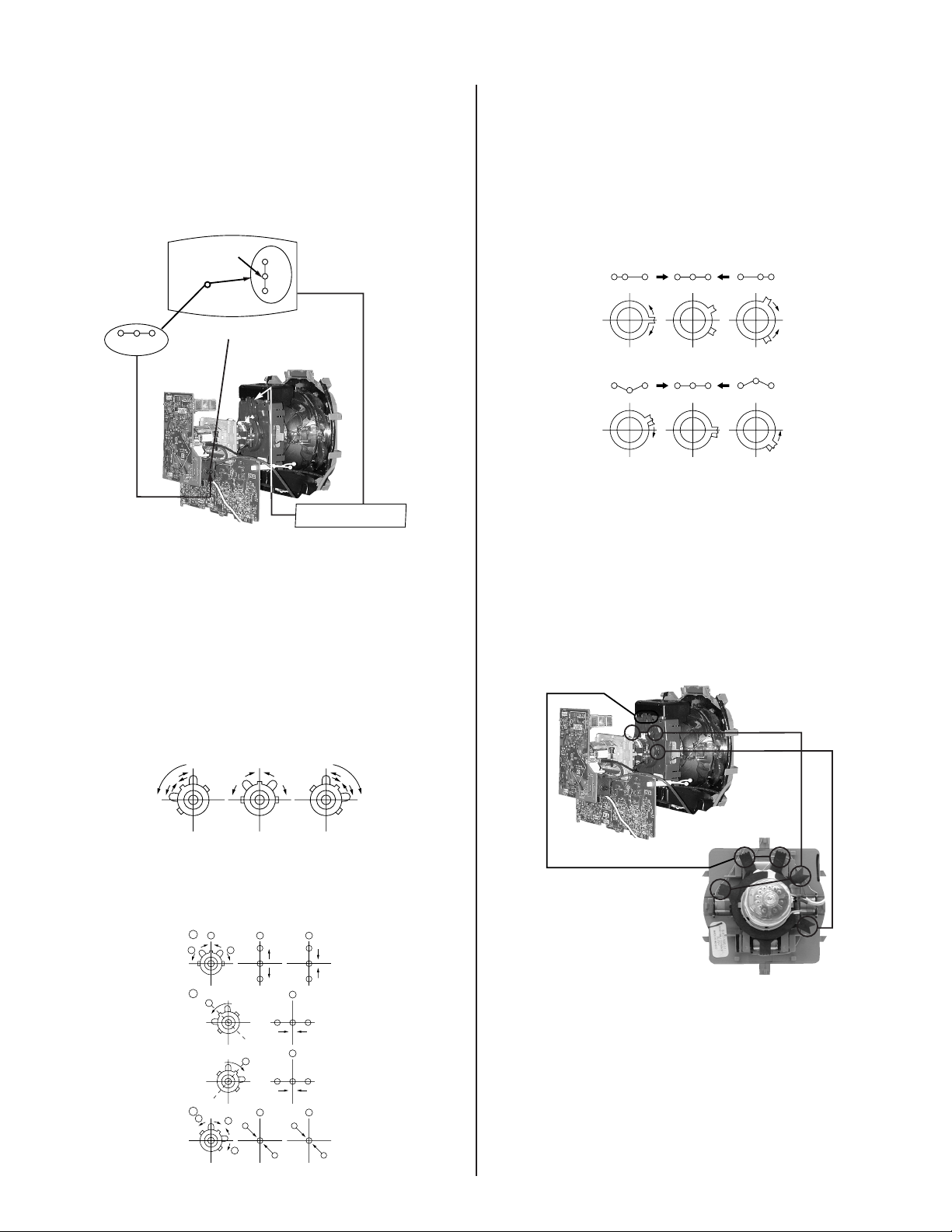
OPERATION OF BMC (HEXAPOLE) MAGNET
The respective dot positions resulting from moving each magnet interact,
so perform adjustment while tracking.
1 Use the V.STAT tabs to adjust the red, green, and blue dots so they
line up at the center of the screen (move the dots in a horizontal
direction).
RG B
RGB RGB
RGB
RGB
RGB
Y SEPARATION AXIS CORRECTION MAGNET
ADJUSTMENT
VERTICAL AND HORIZONTAL STATIC
CONVERGENCE
1. Adjust V. STAT magnet to converge red, green and blue dots in the
center of the screen (Vertical movement).
Tilt the V. STAT magnet and adjust static convergence to open or
close the V. STAT magnet.
2. When the V. STAT magnet is moved in the direction of arrow a and b,
red, green, and blue dots move as shown below:
1
a
b
2
a
a
B
b
G
R
B
G
R
a
RG B
b
1. Input cross-hatch pattern, adjust PICTURE to minimum and
BRIGHTNESS to normal.
2. Adjust the defl ection yoke upright so it touches the CRT.
3. Adjust so that the Y separation axis correction magnet on the neck
assembly is symmetrical from top to bottom (open state).
V. STAT
BMC MAGNET
PURITY
4. Return the defl ection yoke to its original position.
a
G
BG R
B
B
b
b
G
R
b
3
b
a
R
b
— 13 —
KV-27FV300/29FV300/32FV300/36FV300
DYNAMIC CONVERGENCE ADJUSTMENT
Before starting, perform Vertical and Horizontal Static Convergence
Adjustment.
1. Slightly loosen defl ection yoke screw.
2. Remove defl ection yoke spacers.
3. Move the defl ection yoke for best convergence as
shown below:
BGR
R
B
G
G
R
B
B
G
R
RGB
RGB
G
B
BGR RGB
R
G
B
R
RGB
BGR
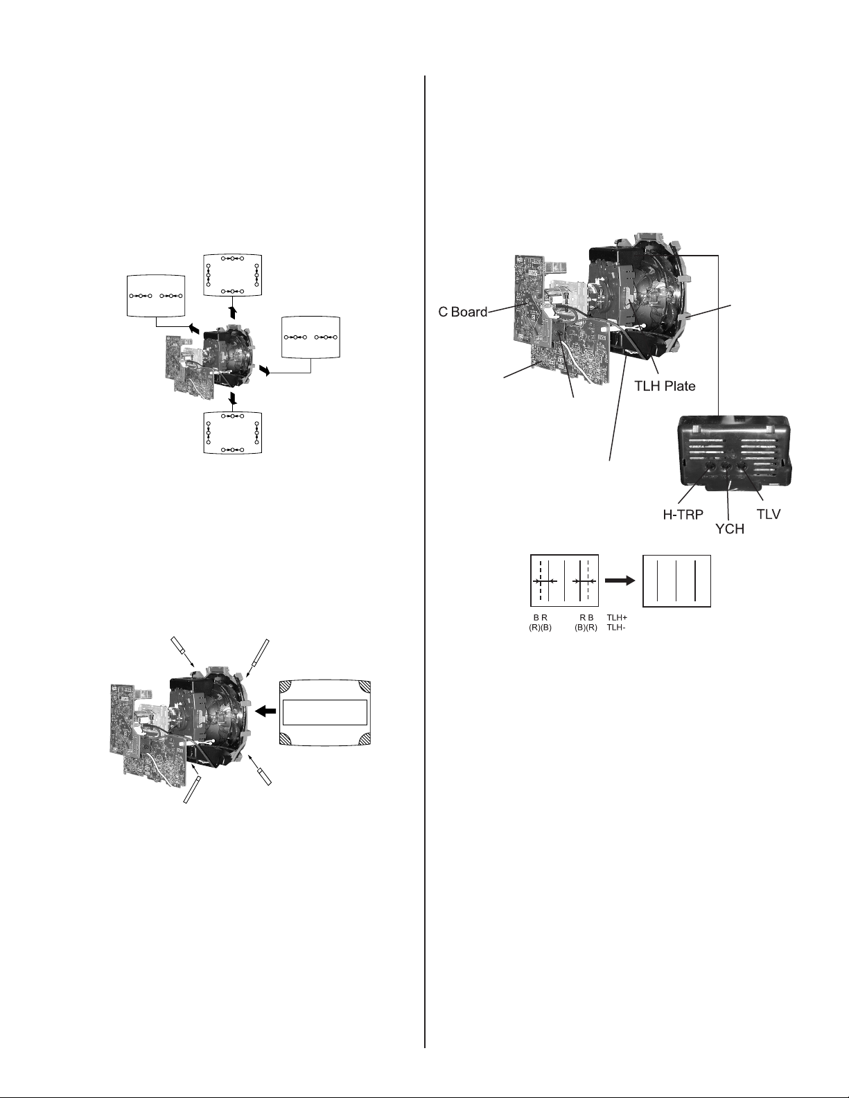
TLH PLATE ADJUSTMENT
Preparation:
• Input crosshatch pattern.
• Adjust Picture Quality to standard, Picture and Brightness to 50%, and
Other to standard.
• Adjust the Horizontal Convergence of red and blue dots by tilting the
TLH plate on the defl ection yoke.
Y Magnet
WA Board
RV701
V. STAT
XCV
4. Tighten the defl ection yoke screw.
5. Install the defl ection yoke spacers.
SCREEN-CORNER CONVERGENCE
1. Affi x a permalloy assembly corresponding to the misconverged areas:
b
a
1. Adjust XCV core to balance X axis.
ba
a-d: screen-corner
misconvergence
cd
c
d
2. Adjust YCH VR to balance Y axis.
3. Adjust vertical red and blue convergence with V.TILT (TLV VR.)
4. Adjust Y MAGNET to correct V.BOW Geometry Distortion.
5. Adjust H-TRP to correct H.Trapezoid Geometry Distortion.
After adjusting items 4 and 5, confi rm overall geometry again.
Perform adjustments while tracking items 1 and 2.
— 14 —
KV-27FV300/29FV300/32FV300/36FV300
2-3. FOCUS
1. Input monoscope signal.
2. Set user controls to normal.
3. Set video mode to STANDARD.
4. Set the PICTURE to maximum.
5. Adjust at 325 Mark for best center/corner focus balance.
6. Receive an entire white signal. Make sure Magenta Ring is at an
acceptable level.
Focus
Screen (G2)
325 MARK
35
35 MARK
CENTER
CIRCLE
325
2-5. WHITE BALANCE ADJUSTMENTS
Adj. NO. Disp. Item All Models
VID_ADJ 0 RDRV Red Drive 41
VID_ADJ 1 GDRV Green Drive 32
VID_ADJ 2 BDRV Blue Drive 29
VID_ADJ 3 RCUT Red Cut-off 31
VID_ADJ 4 GCUT Green Cut-off 14
VID_ADJ 5 BCUT Blue Cut-off 17
VP2 4 SBRT Sub Bright 16
1. Set program palette to STANDARD and push RESET.
2. Input an entire white signal.
3. Set to Service Adjustment Mode.
4. Set the PICTURE and BRIGHT to minimum.
5. Adjust with SBRT if necessary.
6. Set RCUT to “14”.
7. Select GCUT and BCUT with
8. Adjust by pressing
1
and
9. Set the PICTURE and BRIGHT to maximum.
10. Select GDRV and BDRV with and .
11. Adjust with 3 and 6 for the best white balance.
12. Write into the memory by pressing
13. Repeat steps 1-12 for GDR4, BDR4, GCU4 and BCU4 using
Video 4 input.
3
and 5 .
4
for the best white balance.
5
3
then
.
2-4. SCREEN (G2)
1. Input dot pattern from the pattern generator.
2. Set the user controls to NORMAL.
3. Attach the G2-Jig to the C Board.
4. Adjust RCUT, GCUT, BCUT, and SBRT in service mode with an
oscilloscope so that voltages on the red, green, and blue cathodes
are 170 ± 2.0Vdc.
5. Observe the screen and adjust SCREEN (G2) VR to obtain the
faintly visible background of dot signal.
6. Push the TEST + JUMP (+ Channel) to cut off the signal. The screen
should be bright or dark. Brightness of raster must be increased
when adjusting.
7. Adjust screen VR until the screen is slightly cut off, or scarcely lights
up. A signal cannot be seen when the brightness of the raster is
high.
8. Push the JUMP again to release the cut off.
* Use values from Sub Contrast Adjustments
White balance should be adjusted after Sub Contrast because
RDRV is also used in Sub Contrast Adjustment. (See page 22).
170 + 2.0 Vdc
GND
170Vdc
pedestal
— 15 —
SECTION 3: SAFETY RELATED ADJUSTMENTS
KV-27FV300/29FV300/32FV300/36FV300
3-1. X R530, R531 CONFIRMATION METHOD
(HOLD-DOWN CONFIRMATION) AND
READJUSTMENTS
Always perform the following adjustments when replacing the following
components marked with a
Y
mark on the schematic diagram:
Part Replaced () Adjustment ()
A BOARD: HV HOLD DOWN
R550, T503, T504, D519,
R530, R531
IC501, R533, D521, R532,
D520, C531, R529, R530,
R531, C532
PREPARATION BEFORE CONFIRMATION
1. Using a Variac, apply AC input voltage: 120+2.0 VAC.
2. Turn the POWER switch ON.
3. Input a white signal and set the PICTURE and BRIGHT controls to
maximum.
4. Confi rm that the voltage of more than 23.0 VDC appears between
TP85 and ground on the A Board.
HOLD-DOWN READJUSTMENT
If the setting indicated in Step 2 of Hold-Down Operation Confi rmation
cannot be met, readjustment should be performed by altering the
resistance value of R530, R531 component marked with
digital multimeter
+
-
T503
FBT
FBT
R531
R530
TP85
TP85
ammeter
3mA DC range
A
+
-
DC Power Supply
+
-
Figure 1
X
.
HOLD-DOWN OPERATION CONFIRMATION
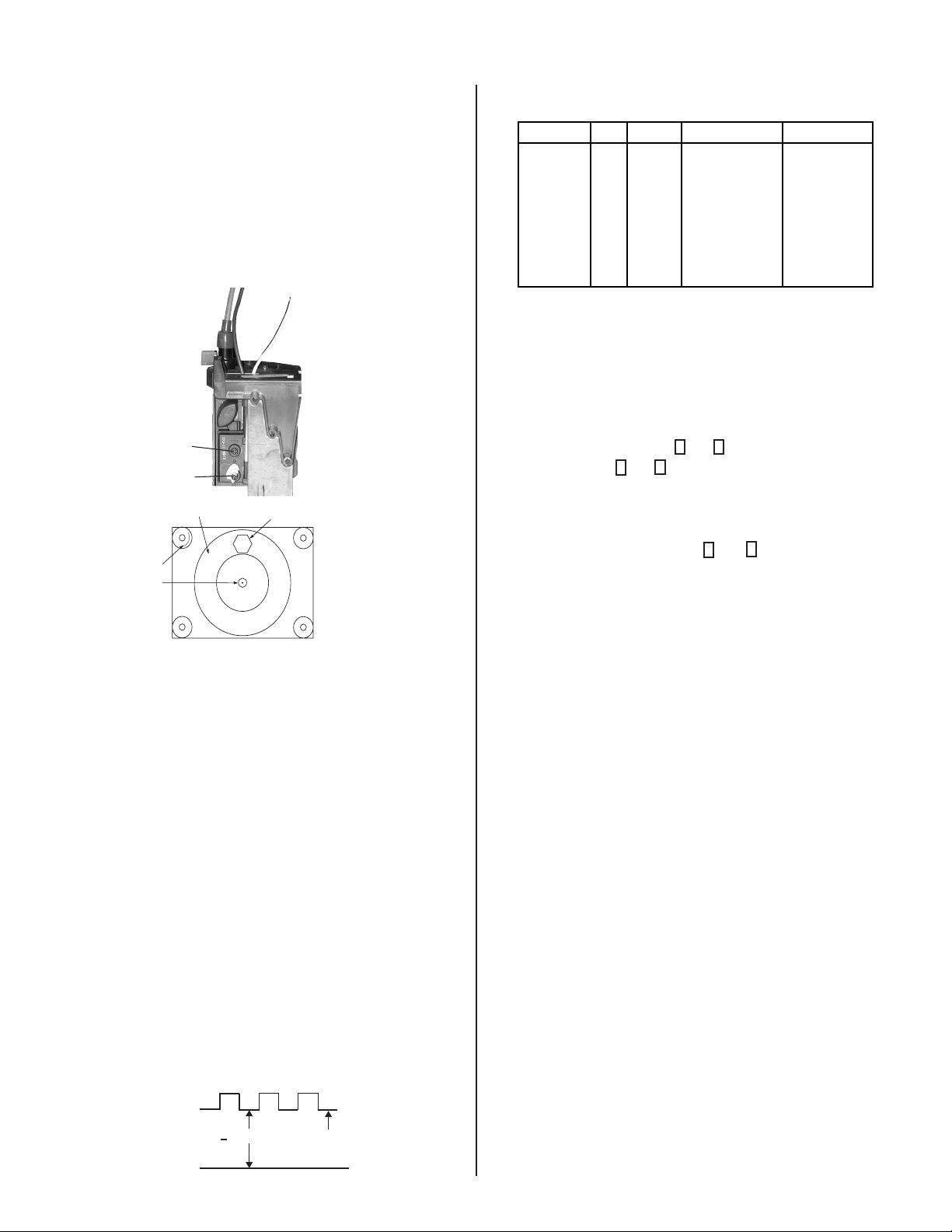
1. Connect the current meter between Pin 11 of the FBT (T503) and the
PWB land where Pin 11 would normally attach. (See Figure 1).
2. Input a dot signal and set PICTURE and BRIGHTNESS to minimum:
IABL = 2175 + 100/ -325 µA.
3. Confi rm the voltage of A Board TP91 is 135 ± 1.5 VDC.
4. Connect the digital voltmeter and the DC power supply to TP85 and
ground. (See Figure 1 above).
5. Increase the DC power voltage gradually until the picture blanks out.
6. Turn DC power source off immediately.
7. Read the digital voltmeter indication (standard = 27.24 + 0.0/ - 0.1
VDC).
8. Input a white signal and set PICTURE and BRIGHTNESS to
maximum: IABL = 2175 + 100/ -325 µA.
9. Repeat steps 4 to 7.
3-2. B+ VOLTAGE CONFIRMATION AND
ADJUSTMENT
Always perform the following adjustments when replacing the following
components, which are marked with
the GK Board:
GK BOARD: IC600, PH602
1. Using a Variac, apply AC input voltage: 130 + 2.0/-0.0 VAC
2. Input a monoscope signal.
3. Set the PICTURE control and the BRIGHT control to
minimum.
4. Confi rm the voltage on A Board between TP23 and ground is less
than 136.5 VDC.
5. If step 4 is not satisfi ed, replace R530 and R531 on A Board and
repeat the above steps.
Y
on the schematic diagram on
— 16 —
SECTION 4: CIRCUIT ADJUSTMENTS
ELECTRICAL ADJUSTMENTS BY REMOTE COMMANDER
Use the Remote Commander (RM-Y181, RM-Y182) to perform the circuit adjustments in this section.
Test Equipment Required: 1. Pattern generator 2. Frequency counter 3. Digital multimeter 4. Audio oscillator
KV-27FV300/29FV300/32FV300/36FV300
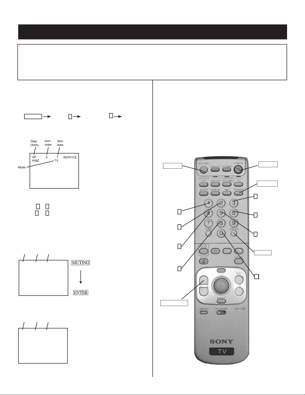
4-1. SETTING SERVICE ADJUSTMENT MODE
1. Standby mode (Power off).
2. Press the following buttons on the remote commander within a
second of each other:
DISPLAY
Channel 5 Sound Volume
+
Power
SERVICE ADJUSTMENT MODE IN
3. The CRT displays the item being adjusted.
4. Press
5. Press
1
or 2 on the Remote Commander to select the item.
3
or 6 on the Remote Commander to change the data.
6. Press MUTING then ENTER to write into memory.
SERVICE ADJUSTMENT MODE MEMORY
Item
order
0
TV
Item
data
7
SERVICE
Green
Red
Disp.
(Item)
VP
HSIZ
4-2. MEMORY WRITE CONFIRMATION
METHOD
1. After adjustment, pull out the plug from the AC outlet, then replace
the plug in the AC outlet again.
2. Turn the power switch ON and set to Service Mode.
3. Call the adjusted items again to confi rm they were adjusted.
4-3. REMOTE ADJUSTMENT BUTTONS AND
INDICATORS
MUTING
(Enter into
memory)
1
Disp. (Item up)
2
(Device Item Up)
4
Disp. (Item down)
8
(Initialize)
POWER
(Service Mode)
DISPLAY
(Service Mode)
3
Item
(Data up)
6
Item
(Data down)
5
(Device item
down)
ENTER
(Enter into
memory)
0
(Remove from
memory)
7. Press then on the Remote Commander to initialize.
Item
order
0
TV
Item
data
7
WRITE
Disp.
(Item)
VP
HSIZ
8. DO NOT turn off set until SERVICE appears.
VOLUME (+)
(Service Mode)
RM-Y182
— 17 —
SERVICE DATA LISTS4-4.
Non-Volatile Memory (NVM) Reference for BA5D Service List
KV-27FV300/29FV300/32FV300/36FV300
Service
VERSION 0 VER 11111111 = = 0
Service
No. Name Bit Mask
Group
Microprocessor version information
Name
Fix /
Var
Vertical Count Down Mode Switching (for
TV)
Vertical Count Down Mode Switching (for
Video)
No.
Group
VP1 0 HSIZ Var H SIZE (11/ 2-7) 11111100 A4 A8 A4 B4
1 HPOS Var HPOS (12 / 2-7) 11111100 A4 A9 A4 B5
2 VBOW Var AFC BOW (16 / 4-7) 11110000 A4 AE A4 BA
3 VANG Var AFC ANGLE (16 / 0-3) 00001111 A4 AE A4 BA
4 VTRP Var TRAPEZIUM (20 / 3-7) 11111000 A4 AF A4 BB
5 HTRP Var H. TRAPEZOID (15 / 4-7) 11110000 A4 AD A4 B9
6 TROT Fix TILT ROTATION (0-63) 11111100 A4 A4 A4 B0
7 PAMP Var PIN AMP (13 / 2-7) 11111100 A4 AA A4 B6
8 UPIN Var UP-CPIN (14 / 2-7) 11111100 A4 AB A4 B7
9 LPIN Var LO-CPIN (1C / 2-7) 11111100 A4 AC A4 B8
10 VSIZ Var V SIZE (0E / 2-7) 11111100 A4 A5 A4 B1
11 VPOS Var V POSITION (0E / 2-7) 11111100 A4 A6 A4 B2
12 VLIN Var V LINEARITY (10 / 0-3) 00001111 A4 A7 A4 B3
13 SCOR Var S CORRECTION (10 / 4-7) 11110000 A4 A7 A4 B3
14 VZOM Fix 16:9 CRT Z Mode on/off 10000000 A4 85
15 EHT Fix Vertical High-Voltage Compensation 00001111 A4 80
16 ASP Fix Aspect Ratio control (4:3 Mode) 11111100 A4 FB 47
17 ASP1 Fix Aspect Ratio control (16:9 Mode) 11111100 A4 FC 47
18 SCRL Fix 16:9 CRT Z Mode Trans. Scroll 00111111 A4 86
19 HBLK Fix Horizontal Blanking on/off 00010000 A4 85
20 LBLK Fix Left Blanking Adjustment 11110000 A4 80
21 RBLK Fix Rigth Blanking Adjustment 00001111 A4 81
22 HDW Fix Horizontal Drive Pulse Width 00001000 A4 85
23 EWDC Fix "Parabola" EW, D.C. Adjustment 00000100 A4 88
24 LVLN Fix Lower Screen BTM Vertical Line Adj. 11110000 A4 81
25 UVLN Fix Uppe Screen BTM Vertical Line Adj. 00001111 A4 82
26 INTL Fix INTERLACE 00110000 A4 84
27 HOSC Fix Horizontal VCO Oscillation Freq. 11110000 A4 82
28 VSS Fix Vertical Sync Slice Level 11000000 A4 84
29 HSS Fix Horizontal Sync Slice Level 00001000 A4 88
30 HMSK Fix For Macro Vision 00010000 A4 88
31 VTMS Fix Select Signal VTIM Pin 01100000 A4 85
32 TCMD Fix
33 VCMD Fix
34 AFC Fix AFC Loop Gain Switching 11000000 A4 86
35 FIFR Fix Field Frequency 11000000 A4 87
36 VBLK Fix VBLKW 00000011 A4 88
37 HTSW Fix H-Trap Switch : NEW 00100000 A4 88
Description
Description Bit Mask
00000011 A4 8C
00000011 A4 8D
Common
Slave Sub Init
Addr Addr Data
Slave Sub Fix Var Slave Sub Slave Sub
Addr Addr Data Data Addr Addr Data Addr Addr Data
PAL-NNTSC / PAL-MCommon
— 18 —
SERVICE DATA LISTS
KV-27FV300/29FV300/32FV300/36FV300
Service
No. Name
Group
VP2 0 REFP Fix REFP 01000000 A4 88 0
1 JPSW Fix Jump SW 00000001 = =
2 SHUE Var Sub HUE adjustment 11110000 A4 8C
3 SCOL Var Sub COLOR adjustment 00001111 A4 8E A4 90 7 A4 92
4 SBRT Var Sub BRIGHTNESS adjustment 00011111 A4 87
5 AXPL Fix Axis PAL 00000001 A4 89 0
6 AXNT Fix Axis NTSC 00000010 A4 89 1
7 CBPF Fix Chroma BPF on/off 00000100 A4 89 1
8 CTRP Fix Y TRAP FILTER on/off 00000001 = =
9 COFF Fix Color On/off 00000010 = =
10 KOFF Fix Set Color Killer 00100000 A4 89 0
11 SSHP Fix Sub SHARPNESS 11110000 A4 83
12 TSPF Fix SHARPNESS Circuit Fo (for TV) 00001100 A4 8C
13 VSPF Fix SHARPNESS Circuit Fo (for Video) 00001100 A4 8D
14 PREL Fix Pre-Shoot/ Over-Shoot 01000000 A4 89 1
15 ABLM Fix ABL Mode Switch 10000000 A4 89 1
16 VTH Fix ABL CD VHT Switching 00000001 = =
17 YDEL Fix Y Delay Time Control 00001111 A4 84
18 NCOL Fix No Color ID 00000001 A4 85
19 FSC Fix FSC Out on/off 00000010 A4 85 1
20 KID Fix Killer ID Control on/off 00000100 A4 85 0
Service
No. Name
Group
VID_ADJ 0 RDRV var R DRIVE (0A / 7-2) 11111100 A4 9E 41
1 GDRV Var G DRIVE (0B / 7-2) 11111100 A4 9F
2 BDRV Var B DRIVE (0C / 7-2) 11111100 A4 A0
3 RCUT Var R CUT OFF ( 07 / 7-2) 11111100 A4 A1 31
4 GCUT Var G CUT OFF (08 / 7-2) 11111100 A4 A2
5 BCUT Var B CUT OFF (09 / 7-2) 11111100 A4 A3
6 SCON Var Sub Contrast adjusment 00001111 A4 8A
7 CHUE Var Sub HUE adjustment for TV 00011111 A4 94 16
8 CCOL Var Sub COLOR adjustment for TV 00011111 A4 8F 18 A4 91 18 A4 93 23
9 UOFS Var YUV U offset 00001111 A4 8B
10 VOFS Var YUV V offset 11110000 A4 8B
11 RON Fix R ON (01 / 3) 00001000 = =
12 GON Fix G ON (01 / 2) 00000100 = =
13 BON Fix B ON (01 / 1) 00000010 = =
14 HUEV Var Sub HUE adjustment for Video 11110000 A4 8D
15 COLV Var Sub COLOR adjustment for Video 11110000 A4 8E A4 90 A4 92
Fix /
Var
Fix /
Var
Description Bit Mask
Description Bit Mask
Slave Sub Fix Var Slave Sub Slave Sub Slave Sub
Addr Addr Data Data Addr Addr Data Addr Addr Data Addr Addr Data
Slave Sub Fix Var Slave Sub Slave Sub Slave Sub
Addr Addr Data Data Addr Addr Data Addr Addr Data Addr Addr Data
PAL-NCommon NTSC PAL-M
NTSC PAL-M PAL-NCommon
— 19 —
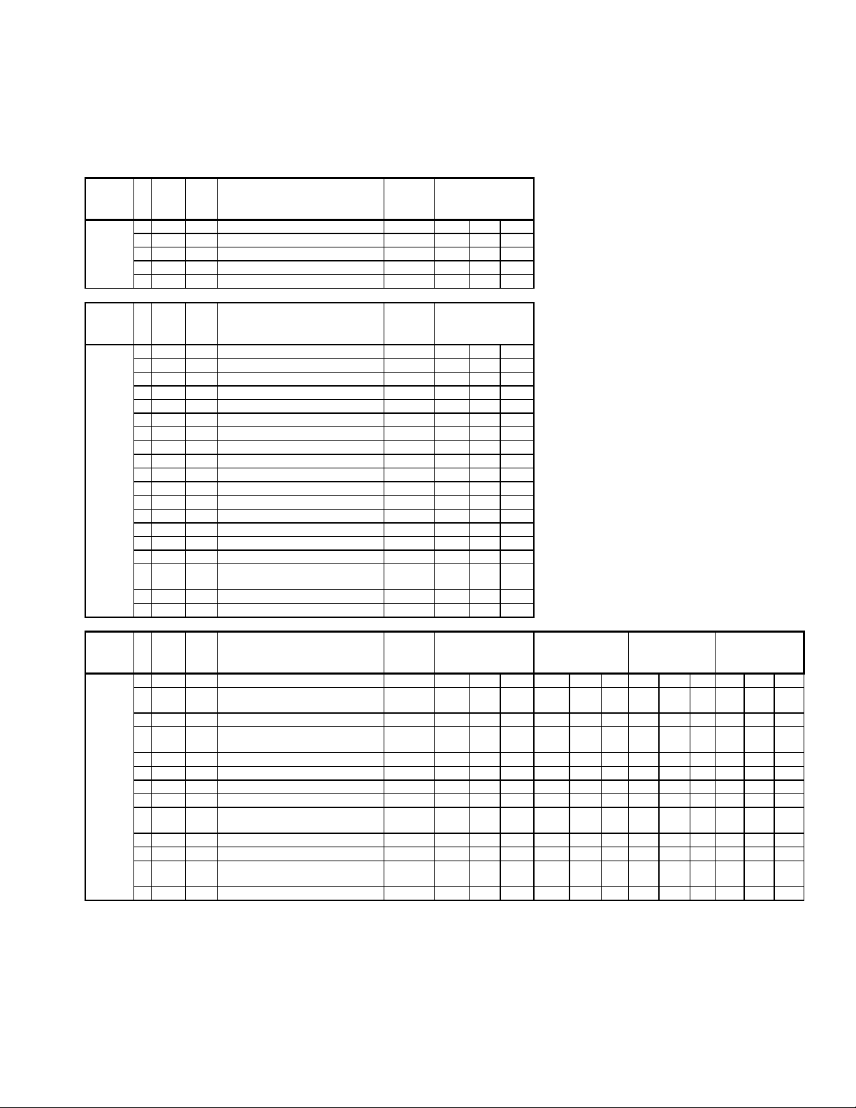
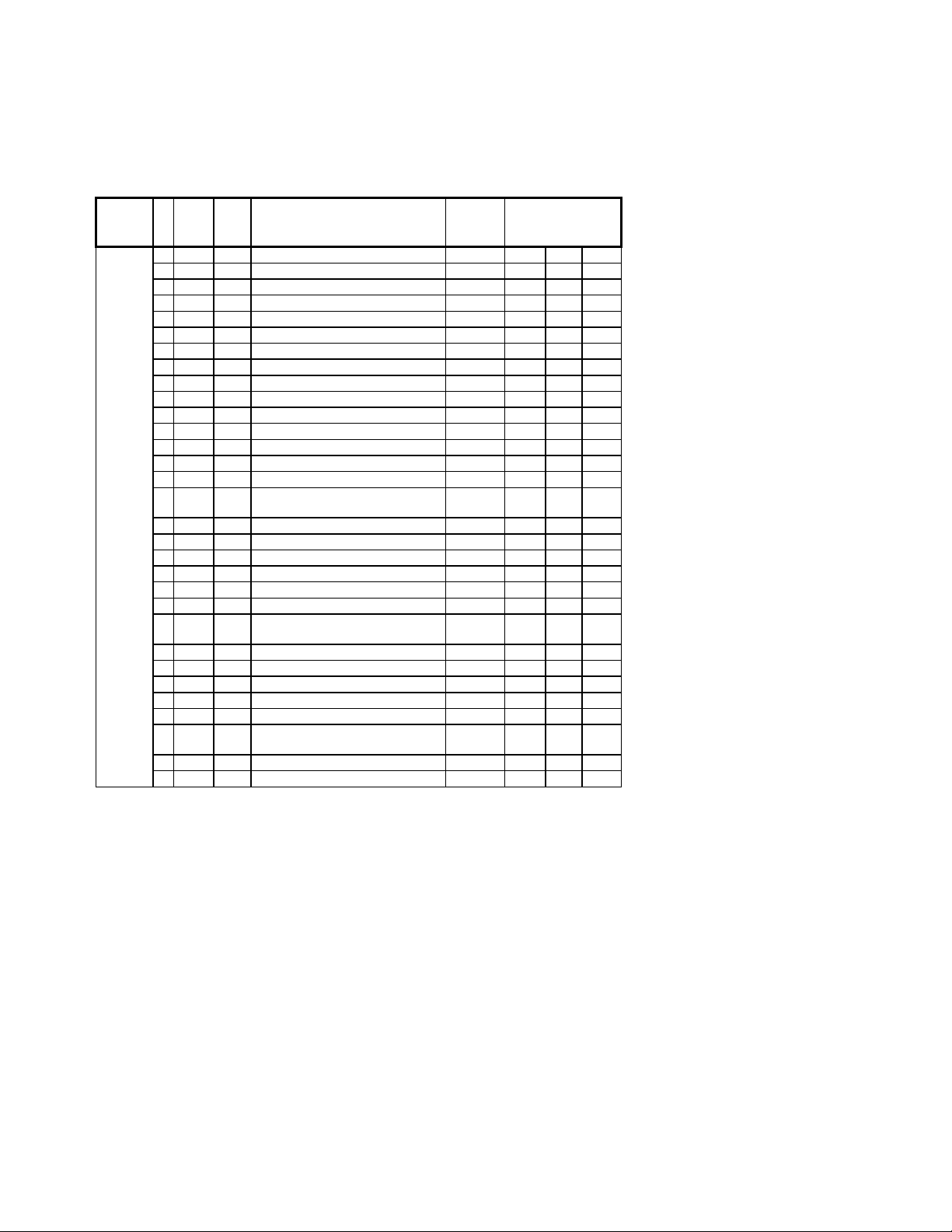
SERVICE DATA LISTS
KV-27FV300/29FV300/32FV300/36FV300
Service
No. Name
Group
COL_TMP 0 GDOF Fix G DRIVE Offset 11111000 A4 9A 4
Service
Group
PIC_IMP 0 BLAD Fix Black area detect (01 / 6-7) 11000000 A4 09 0
1 BDOF Fix B DRIVE Offset 11111000 A4 9B 15
2 GCOF Fix G CUT Offset 11111000 A4 9C 7
3 BCOF Fix B CUT Offset 11111000 A4 9D 14
4 DCOL Fix Dinamic Color 00000010 = =
No. Name
1 SRTS Fix SRT level (01 / 4-5) 00110000 A4 09 3
2 YNR Fix YNR(01 / 2) 00000100 A4 09 1
3 GIRE Fix Gamma correction(01 / 0-1) 00000011 A4 09 3
4 DAC1 Fix DAC1(02 / 7) 10000000 A4 0A 0
5 DAC2 Fix DAC2(02 / 6) 01000000 A4 0A 0
6 VMGA Fix VM on 1226 (02/5-4) 00110000 A4 0A 0
7 GCUR Fix Gamma curve(02 / 2) 00000100 A4 0A 1
8 BLKC Fix Black Compensation (02 / 1) 00000010 A4 0A 1
9 TEST Fix TEST(03 / 6-7) 11000000 A4 0B 3
10 RS Fix RS (03 / 3-5) 00111000 A4 0B 0
11 RTC Fix RTC(03 / 0-2) 00000111 A4 0B 2
12 APAC Fix APAC 10000000 A4 0B 0
13 SRTH Fix SRT bit for Dynablack = High 10000000 A4 5C 1
14 SRTL Fix SRT bit for Dynablack = Low 10000000 A4 5D 1
15 SRTO Fix SRT bit for Dynablack = Off 10000000 A4 5E 0
16 SHPH Fix Sharpness level for Dynablack = High 01111111 A4 5C 54
17 SHPL Fix Sharpness level for Dynablack = Low 01111111 A4 5D 43
18 SHPO Fix Sharpness level for Dynablack = Off 01111111 A4 5E 0
Fix /
Var
Fix /
Var
Description Bit Mask
Description Bit Mask
Common
Slave Sub Fix
Addr Addr Data
Common
Slave Sub Fix
Addr Addr Data
Service
No. Name
Group
PALETTE 0 VPIC Fix User picture setting 0:min, 63: max 11111100 A4 5F 63 A4 65 50 A4 6B 38 A4 71 63
1 VBRT Fix User brightness setting 0:min, 63: max 11111100 A4 60 31 A4 66 31 A4 6C 31 A4 72 31
2 VCOL Fix User color setting 0:min, 63: max 11111100 A4 61 35 A4 67 31 A4 6D 31 A4 73 40
3 VSHP Fix User sharpness setting 0:min, 63: max 11111100 A4 62 31 A4 68 31 A4 6E 34 A4 74 31
4 VVM Fix 0: OFF, 1: Low, 2: High, 3: N/A 00000011 A4 5F 2 A4 65 1 A4 6B 0 A4 71 2
5 VTRI Fix 0: Cool, 1: Nutral, 2: Warm, 3: N/A 00000011 A4 60 0 A4 66 1 A4 6C 2 A4 72 0
6 VGMA Fix 0: OFF, 1: Low, 2: Mid, 3: Max 00000011 A4 63 2 A4 69 2 A4 6F 2 A4 75 2
7 VNRM Fix 0: 3D, 1: 2D 00000010 A4 61 0 A4 67 0 A4 6D 0 A4 73 0
8 VYDC Fix
9 VVEN Fix Vertoca; Enhancement 00011100 A4 63 5 A4 69 3 A4 6F 3 A4 75 5
10 VHK0 Fix Horizontal Peaking 0:On, 1:Off 00000001 A4 61 0 A4 67 0 A4 6D 0 A4 73 0
11 VDBK Fix
12 VYPL Fix Y-Peaking Limit 00000011 A4 64 1 A4 6A 0 A4 70 0 A4 76 1
Fix /
Var
DC Transmission Ratio 0,1: 100%, 2:
92%, 3: 85
User Dynablack 0: OFF, 1: Low, 2: High,
3: N/A
Description Bit Mask
00000011 A4 62 3 A4 68 3 A4 6E 2 A4 74 3
01100000 A4 63 2 A4 69 1 A4 6F 1 A4 75 1
Palette = VIVID
Slave Sub Fix Slave Sub Fix Slave Sub Fix Slave Sub Fix
Addr Addr Data Addr Addr Data Addr Addr Data Addr Addr Data
Palette = SPORTSPalette = STANDARD Palette = MOVIE
— 20 —
SERVICE DATA LISTS
KV-27FV300/29FV300/32FV300/36FV300
Service
3L_COMB 0 FUNN Fix Function (0 / 7-6) for NTSC 11000000 A4 3C 3
Service
3D_COMB 0 COUT Fix COUTS(00 / 2-3) 00001100 A4 21 3
Group
Group
No. Name
1 FUNP Fix Function (0 / 7-6) for PAL-N, PAL-M 00110000 A5 3C 3
2 DRNG Fix DRANG (0 / 2) 00000100 A4 3C 0
3 YCSM Fix Y/C Sep Mode (0 / 1-0) 00000011 A4 3C 0
4 CNRK Fix CNRK (1 / 7-6) 11000000 A4 3D 1
5 CNRL Fix CNR Lim (1 / 5-4) 00110000 A4 3D 1
6 CLPF Fix C-LPF(1 / 3) 00001000 A4 3D 1
7 SLPF Fix SelC-LPF(1 / 2) 00000100 A4 3D 0
8 MODE Fix Mode1 (1 / 1) 00000010 A4 3D 0
9 YPG Fix Y - Peaking Gain (2 / 7-6) 11000000 A4 3E 3
10 PDSC Fix Pds. Clip (2 / 3) 00001000 A4 3E 0
11 YLPF Fix Y-LPF(2 / 2) 00000100 A4 3E 1
12 VENL Fix V-Emph N.L (3 / 4-2) 00011100 A4 3F 4
13 VEC Fix V - Emph Core (3 / 1-0) 00000011 A4 3F 3
No. Name
1 YAPS Fix YAPS(00 / 0-1) 00000011 A4 21 1
2 NSDS Fix NSDS(01 / 4-5) 00110000 A4 22 0
3 MSS Fix MSS(01 / 2-3) 00001100 A4 22 0
4 KILS Fix KILS (01 / 1-0) 00000011 A4 22 1
5 DYC Fix DYCOS ( 02 / 7-6) 11000000 A4 23 2
6 EXAD Fix EXADINS(02 / 5) 00100000 A4 23 0
7 EXCS Fix EXCSS(02 / 1- 0) 00000011 A4 23 1
8 CPP Fix CPP(03 / 6) 01000000 A4 24 0
9 HDP Fix HDP(03 / 3-5) 00111000 A4 24 6
10 CDL Fix CDL(03 / 0-2) 00000111 A4 24 6
11 DYCO Fix DYCOR(04 / 4-7) 11110000 A4 25 2
12 DYGA Fix DYGAIN(04 / 0-3) 00001111 A4 25 10
13 DCCO Fix DCCOR(05 / 4-7) 11110000 A4 26 2
14 DCGA Fix DCGAIN(05 / 0-3) 00001111 A4 26 9
15 YNRL Fix YNRLIM(06 / 4-5) 00110000 A4 27 1
16 CNRL Fix CNRLIM(06 / 0-1) 00000011 A4 27 1
17 ID1O Fix ID1ON(07 / 7) 10000000 A4 28 0
18 ID1W Fix ID1W0A1(07 / 6) 01000000 A4 28 0
19 ID1N Fix ID1W0A2(07 / 5) 00100000 A4 28 0
20 WSC Fix WSC(08 / 6-7) 11000000 A4 29 1
21 VTRH Fix VTRH(08 / 4-5) 00110000 A4 29 1
22 VTRR Fix VTRR(08 / 2-3) 00001100 A4 29 1
23 LDSR Fix LDSR(08 / 0-1) 00000011 A4 29 2
24 WSS Fix WSS(09/7) 10000000 A4 2A 0
25 ID1E Fix ID1ECON ( 09/6) 01000000 A4 2A 1
26 TT Fix TT ( 09 / 4 -5) 00110000 A4 2A 0
27 FELC Fix FELCHK ( 09/3) 00001000 A4 2A 1
28 TH Fix TH ( 09 / 1 -2) 00000110 A4 2A 0
29 VAPG Fix VAPGAIN(0A / 5-7) 11100000 A4 2B 3
30 VAPI Fix VAPINV(0A / 0-4) 00011111 A4 2B 25
Fix /
Var
Fix /
Var
Description Bit Mask
Description Bit Mask
Common
Slave Sub Fix
Addr Addr Data
Common
Slave Sub Fix
Addr Addr Data
— 21 —

SERVICE DATA LISTS
KV-27FV300/29FV300/32FV300/36FV300
Service
3D_COMB 31 YPFT Fix YPFT(0B / 4-5) 00110000 A4 2C 3
Group
No. Name
32 YPFG Fix YPFG(0B / 0-3) 00001111 A4 2C 8
33 V1PS Fix V1PS(0C / 6-7) 11000000 A4 2D 3
34 VEGS Fix VEGS(0C / 4-5) 00110000 A4 2D 2
35 CC3N Fix CC3N(0C / 3) 00001000 A4 2D 0
36 C0HS Fix C0HS(0C / 2) 00000100 A4 2D 0
37 SEL2 Fix SELD2FH(0C / 0) 00000001 A4 2D 1
38 SEL1 Fix SELD1FL(0D / 5) 00100000 A4 2E 1
39 YHCO Fix YHCOR(10 / 6-7) 11000000 A4 31 0
40 YHCG Fix YHCGAIN(10 / 5) 00100000 A4 31 1
41 OVST Fix +OVST(10 / 3) 00001000 A4 31 0
42 CSHD Fix CSHDT(10 / 2) 00000100 A4 31 0
43 KCTT Fix KCTT(10 / 0-1) 00000011 A4 31 0
44 SHT Fix SHT(11 / 7-6 ) 11000000 A4 32 0
45 VCT Fix VCT(11/ 5) 00100000 A4 32 0
46 CGAT Fix CLKGAT ( 11 / 4) 00010000 A4 32 0
47 CG2D Fix CLK2D ( 11 / 3) 00001000 A4 32 1
48 CGGT Fix CLKGGT ( 11 / 2) 00000100 A4 32 0
49 CGEB Fix CLKGEB ( 11 / 1) 00000010 A4 32 0
50 CGT Fix CLKGT ( 11 / 0) 00000001 A4 32 0
51 HPLL Fix HPLLFS(12 / 7) 10000000 A4 33 1
52 BPLL Fix BPLLFS (12 / 6) 01000000 A4 33 0
53 FSCF Fix FSCFG(12 /5) 00100000 A4 33 0
54 PLLF Fix PLLFG(12 / 4) 00010000 A4 33 1
55 KILR Fix KILR(12 / 0-3) 00001111 A4 33 3
56 HSSL Fix HSSL(13 / 4-7) 11110000 A4 34 12
57 VSSL Fix VSSL(13 / 0-3) 00001111 A4 34 8
58 BGPS Fix BGPS(14 / 4-7) 11110000 A4 35 4
59 BGPW Fix BGPW(14 / 0-3) 00001111 A4 35 10
60 ADCL Fix ADCLKS(15 / 6-7) 11000000 A4 36 3
61 NSDW Fix NSDSW(15 / 4) 00010000 A4 36 1
62 HIZE Fix HIZEN ( 16 / 4) 00010000 A4 37 0
63 HCNT Fix HCNTFSYN ( 17 / 6) 01000000 A4 38 0
Fix /
Var
Description Bit Mask
Common
Slave Sub Fix
Addr Addr Data
— 22 —
SERVICE DATA LISTS
KV-27FV300/29FV300/32FV300/36FV300
Service
No. Name
Group
PIP 0 PFRN Fix VCXO oscilation 00000010 A4 40 0
1 PRVS Fix
2 PCON Fix PIP sub contrast control 01111111 A4 41 97
3 PUCO Fix PIP U level control 01111111 A4 42 5
4 PVCO Fix PIP V level control 01111111 A4 43 17
5 PHUE Fix PIP sub hue control 00111111 A4 57 12
6 PKIL Fix Color killer 10000000 A4 42 0
7 PSEP Fix C-sync sep input selection 11000000 A4 44 1
8 PDCN Fix Sub pic sync sep. Thereshold setting 00110000 A4 44 3
9 PBGS Fix bgp position setting 00111111 A4 45 15
10 PDL0 Fix Y/C delay adjust (for video) 00001111 A4 46 11
11 PDL1 Fix Y/C delay adjust (for yuv) 11110000 A4 46 13
12 PBRT Fix Y bryghtness control 00011111 A4 48 25
13 PVP1 Fix V pedestal level for YUV 11110000 A4 49 0
14 PUP1 Fix U pedestal level for YUV 00001111 A4 49 0
15 PVP2 Fix V pedestal level for main w/ burst 11110000 A4 4A 0
16 PUP2 Fix U pedestal level for main w/ burst 00001111 A4 4A 0
17 PVP3 Fix V pedestal level for main w/o burst 11110000 A4 4B 0
18 PUP3 Fix U pedestal level for main w/o burst 00001111 A4 4B 0
19 PACS Fix 0D, 0Eh setting mode 01000000 A4 4C 1
20 PSYS Fix Color system 00110000 = =
21 PSDL Fix Sync delay control 00000011 A4 4C 0
22 PCCL Fix YUV color level 11110000 A4 4D 11
23 PCGA Fix Croma gain 00001000 A4 4D 0
24 PAAF Fix Auto AFC 00000100 A4 4D 1
Fix /
Var
HD/VD input synchronous mode
selection
Description Bit Mask
00000001 A4 40 1
Common
Slave Sub Fix
Addr Addr Data
— 23 —
SERVICE DATA LISTS
KV-27FV300/29FV300/32FV300/36FV300
Service
No. Name
Group
PIP 25 PSU2 Fix For test 00000010 A4 4D 0
26 PCVF Fix Internal 1H comb filter 00000001 A4 4D 0
27 PBIT Fix Y clamp time constant 10000000 A4 4E 0
28 PAFC Fix AFC time constant 01000000 A4 4E 0
29 PACC Fix Color decoder amplitude 00111111 A4 4E 21
30 PSDT Fix System automatic judgment 10000000 = =
31 PBUR Fix VCXO mode selection 01000000 A4 4F 0
32 PEVE Fix Main picture PAL-N 00100000 A4 4F 0
33 PINW Fix Invert sub picture field definition 00010000 A4 4F 0
34 PINR Fix Invert main picture field definition 00001000 A4 4F 0
35 PVMD Fix Vertical display mode when pal-n 00000100 = =
36 PREF Fix Main picture field fix 00000010 A4 4F 0
37 PARE Fix Automatic 50/60 Hz judgement 00000001 A4 4F 0
38 PBWD Fix BW det. Treshold setting 00110000 A4 50 1
39 PFRA Fix Freq. Adjustment for free run mode 00001111 A4 51 0
40 PPAL Fix Parameter setting for PAL-M judgment 11111111 A4 52 52
41 PHPO Fix Sub picture h position 00111111 A4 58 3
42 PVPO Fix Sub picture v position 00111111 A4 59 22
43 PHTI Fix Display timing adjust 00001111 A4 44 3
44 PHAJ Fix Main/Sub switch delay control 11110000 A4 47 2
45 PBGY Fix Back ground Y level setting 00001111 A4 53 0
46 PCRO Fix Sub picture read mode 10000000 A4 54 0
47 PPAR Fix
48 PHPF Fix Y output HPF 00010000 A4 51 0
49 PFSC Fix FSC output 10000000 A4 43 0
50 PVCH Fix 15h,16h,17h, setting mode 00000100 A4 4C 0
51 PVON Fix V-chip decode mode 10000000 A4 53 1
52 PVLN Fix V-chip data slicer line selection 00011111 A4 54 17
53 PVSB Fix
54 PVLV Fix V-chip data slicer slice parameter 11111111 A4 56 130
55 SUSW Fix Sub-Unlock bit position switch 01000000 A4 59 0
Fix /
Var
Thereshold contol for ident judgement of
sub
V-chip data slicer start bit detection
parameter
Description Bit Mask
00001111 A4 50 1
11111111 A4 55 64
Common
Slave Sub Fix
Addr Addr Data
— 24 —
SERVICE DATA LISTS
KV-27FV300/29FV300/32FV300/36FV300
Service
Service
Service
No. Name
Group
AP 0 SBAL Fix Sub Balance 00000111 A8 41 4 A8 41 4
1 SBAS Fix Sub Bass 00000111 A8 43 4 A8 43 4
2 STRE Fix Sub Treble 00000111 A8 42 0 A8 42 0
3 SRL Fix Surround level 00000001 A8 44 0 A8 44 0
4 BBOH Fix Surround Off - BBE high 11110000 A8 45 10 A8 45 10
5 BBOL Fix Surround Off - BBE low 00001111 A8 45 5 A8 45 5
6 BBSH Fix Simulated - BBE high 11110000 A8 46 0 A8 46 0
7 BBSL Fix Simulated - BBE low 00001111 A8 46 0 A8 46 0
8 BBMH Fix Surround - BBE high 11110000 A8 47 0 A8 47 0
9 BBML Fix Surround - BBE low 00001111 A8 47 0 A8 47 0
10 BBGH Fix WOW - BBE high 11110000 A8 48 6 A8 48 6
11 BBGL Fix WOW - BBE low 00001111 A8 48 9 A8 48 9
12 BBTH Fix Trusurround - BBE high 11110000 A8 49 7 A8 49 7
13 BBTL Fix Trusurround - BBE low 00001111 A8 49 8 A8 49 8
14 VFIX Fix Audio output fix data 11111111 A8 4A 244 A8 4A 244
15 AGCL Fix AGC Level 00000110 A8 44 2 A8 44 2
No. Name
Group
CCD 0 DUM0 Fix Only for testing 11111111 = =
1 VOSD Fix Only for testing 00000001 = =
No. Name
Group
OP 0 DISP Fix OSD Display position 00111111 A4 06 28
1 RAMW Fix 00000001 = =
2 ICMP Fix
3 IPOR Fix 0:Even, 1: Odd, Other: do not change 00000011 A4 3A 1
4 FAWD Fix 1: Forced to auto wide mode, 0:normal 00000100 A0 5D 0
5 HCLW Fix H-Count Lower limit 11111111 A4 02 67
6 HCHG Fix H-Count Higher limit 11111111 A4 03 254
7 9VTM Fix Delay for 9V check subsystem 11111111 A4 04 55
8 ZDET Fix Zero detect relay delay 11111111 A4 05 123
Fix /
Var
Fix /
Var
Fix /
Var
Comparison data to determine Noninterlace signal for OSD
Description Bit Mask
Description Bit Mask
Description Bit Mask
00011111 A4 39 4
KV-27FV300/29FV300 KV-32FV300/36FV300
Slave Sub Fix Var Slave Sub Fix Var
Addr Addr Data Data Addr Addr Data Data
Common
Slave Sub Fix
Addr Addr Data
Common
Slave Sub Fix
Addr Addr Data
Service
No. Name
Group
ID 0 ID0 Fix Model variation ID0 11111111 A4 78
1 ID1 Fix Model variation ID1 11111111 A4 79
2 ID2 Fix Model variation ID2 11111111 A4 7A
3 ID3 Fix Model variation ID3 11111111 A4 7B
4 ID4 Fix Model variation ID4 11111111 A4 7C
5 ID5 Fix Model variation ID5 11111111 A4 7D
6 ID6 Fix Model variation ID6 11111111 A4 7E
7 ID7 Fix Model variation ID7 11111111 A4 7F
Fix /
Var
To determine ID's value, ID map must be refered
Description Bit Mask Var Data
Slave
Addr
— 25 —
Sub
Addr
SEE ID MAP
SEE ID MAP
SEE ID MAP
SEE ID MAP
SEE ID MAP
SEE ID MAP
SEE ID MAP
SEE ID MAP
KV-27FV300/29FV300/32FV300/36FV300
4-5. ID MAP TABLE
Model Destination ID-O ID-1 ID-2 ID-3 ID-4 ID-5 ID-6 ID-7
KV-27FV300 US 89 63 237 98 78 128 6 16
KV-27FV300 CND 89 63 237 82 78 128 6 16
KV-29FV300 E 81 63 237 194 110 128 6 80
KV-32FV300 US 89 63 237 98 78 128 6 24
KV-32FV300 CND 89 63 237 82 78 128 6 24
KV-36FV300 US/HAW 89 63 237 98 78 128 6 24
KV-36FV300 CND 89 63 237 82 78 128 6 24
4-6. A BOARD ADJUSTMENTS
H. FREQUENCY (FREE RUN) CHECK
1. Input a TV mode (RF) with no signal.
2. Connect a frequency counter to base of Q501
(TP-25 H. DRIVE) on the A Board.
3. Check H. Frequency for 15734 ± 400/-200 Hz.
V. FREQUENCY (FREE RUN) CHECK
1. Select video 1 with no signal input.
2. Set the conditions for a standard setting.
3. Connect the frequency counter to TP-27 (V OUT) or CN501 pin
6
(V DY+) and ground on the A Board .
4. Check that V. Frequency shows 60 ± 5 Hz.
SUBCONTRAST ADJUSTMENT (RDRV)
1. Input a color-bar signal and set the level to 75%.
2. Set in Standard mode.
3. Activate the Service Adjustment Mode. Set color min pic max.
4. Set GON and BON items. Using
values. Leave RON set to “1”.
3
and 6 set each to the following
7. Adjust the value of SCON with
3
and 6 for
1.90 ± 0.05Vpp for 27/29/32/34”, or 1.95 ± 0.05Vpp for 36/38”.
8. Reset AALS, ABLS, GON and BON values to “1”.
R ON: ON (1)
G ON: ON (1)
B ON: ON (1)
9. Press
MUTING
then
ENTER
to save into the memory.
DISPLAY POSITION ADJUSTMENT (DISP)
1. Input a color-bar signal.
2. Set to Service Adjustment Mode.
3. Select DISP with
4. Adjust values of DISP with
center.
5. Write to memory by pressing
6. Check to see if the text is displayed on the screen.
Signal
Type
1
and 4 .
3
and 6 to adjust characters to the
MUTING
Mode
Category
service micro disp 48
ntsc
vchp
Display
Item
00000000 00000000
then
Item
Data
ENTER
.
Mode
service video rdrv
Signal
Type
ntsc
vchp
Category
Display
00000000 00000000
Item
26
Item
Data
R ON: ON (1)
G ON: OFF (0)
B ON: OFF (0)
5. Connect an oscilloscope probe to C Board, CN705 pin 3 (Red Out)
(TP35).
6. Select SCON with
1
and 4 .
— 26 —
SUB BRIGHT ADJUSTMENT (SBRT)
1. Input a monoscope signal.
2. Activate the Service Adjustment Mode.
3. Set the PICTURE and BRIGHTNESS to minimum.
4. Select the SBRT item with
5. Adjust the values of SBRT with
1
and 4 .
3
and 6 to obtain a faintly visible
crosshatch.
6. Press
MUTING
then
ENTER
to save into the memory.
SUB HUE, SUB COLOR ADJUSTMENT
(SHUE, SCOL)
1. Input color-bar signal at 75%.
2. Activate the Service Adjustment Mode.
3. Set (PIC) to Max and (COL) to 50%.
4. Connect an oscilloscope probe to C Board, CN705Pin
1
5. Select the SHUE and SCOL item with
and 4 .
4
Blue Out.
KV-27FV300/29FV300/32FV300/36FV300
1
6. While showing the SHUE item, adjust the waveform with
4
and
until the second and third bars show the same level
(V2 = V3 < 0.15Vp-p).
7. While showing the SCOL item, adjust the waveform with
6
and
until the fi rst and fourth bars show the same level
(V1 = V4 < 0.15Vp-p).
8. Press
MUTING
then
V2 V3
V1
ENTER
V4
to save into the memory.
3
V. SIZE ADJUSTMENT (VSIZ)
1. Input a crosshatch signal.
2. Activate the Service Adjustment Mode.
3. Select the VSIZ item with
4. Adjust value of VPOS with
5. Press
MUTING
then
1
and 4 .
1
and 4 for the best vertical center.
ENTER
to save into the memory.
H. SIZE ADJUSTMENT (HSIZ)
1. Input a monoscope signal.
2. Activate the Service Adjustment Mode.
3. Select HSIZ with
4. Adjust with
5. Press
MUTING
1
and 4 .
3
and 6 for the best horizontal size.
ENTER
then
to save into the memory.
V. LINEARITY (VLIN), V. CORRECTION
(SCOR), PIN AMP (PAMP), AND HORIZONTAL
TRAPEZOID (HTRP) ADJUSTMENTS
1. Input a crosshatch signal.
2. Activate the Service Adjustment Mode.
3. Select VLIN, SCOR, PAMP, and HTRP with with
4. Adjust with
5. Press
3
and 6 for the best horizontal size.
MUTING
then
V LINEARITY (VLIN)
ENTER
to save into the memory.
1
and 4.
V. CENTER ADJUSTMENT (VPOS)
Perform this adjustment after performing H. Frequency
(Free Run) Check.
1. Input a crosshatch signal.
2. Activate the Service Adjustment Mode.
3. Select the VPOS item with
4. Adjust value of VPOS with
5. Press
MUTING
then
1
and 4 .
3
and 6 for the best vertical center.
ENTER
to save into the memory.
H. CENTER ADJUSTMENT (HPOS)
Perform this adjustment after performing H. Frequency
(Free Run) Check.
1. Input a crosshatch signal.
2. Activate the Service Adjustment Mode.
3. Select the HPOS item with
4. Adjust the value of HPOS with
5. Press
MUTING
then
1
ENTER
and 4 .
3
and 6 for the best horizontal center.
to save into the memory.
V CORRECTION (SCOR)
PIN AMP (PAMP)
HORIZONTAL TRAPEZOID (HTRP)
— 27 —
V. ANGLE (VANG), V. BOW (VBOW), UPPER
PIN (UPIN) AND LOW PIN (LPIN)
ADJUSTMENTS
1. Input a crosshatch signal.
2. Activate the Service Adjustment Mode.
3. Select VANG, VBOW, UPIN, and LPIN with
4. Adjust with
5. Press
3
and 6 for the best picture.
ENTER
MUTING
then
V ANGLE (VANG)
V BOW (VBOW)
to save into the memory.
1
and 4.
KV-27FV300/29FV300/32FV300/36FV300
UPPER PIN (UPIN)
LOW PIN (LPIN)
SERVICE ADJUSTMENT MODE MEMORY
ENTER
0
Item
then
Item
Data
7
.
Green
0
Red
ENTER
1. After completing all adjustments, press
Read From Memory
Mode
service defl vbow
Signal
Type
ntsc
vchp
Category
Display
00000000 00000000
— 28 —
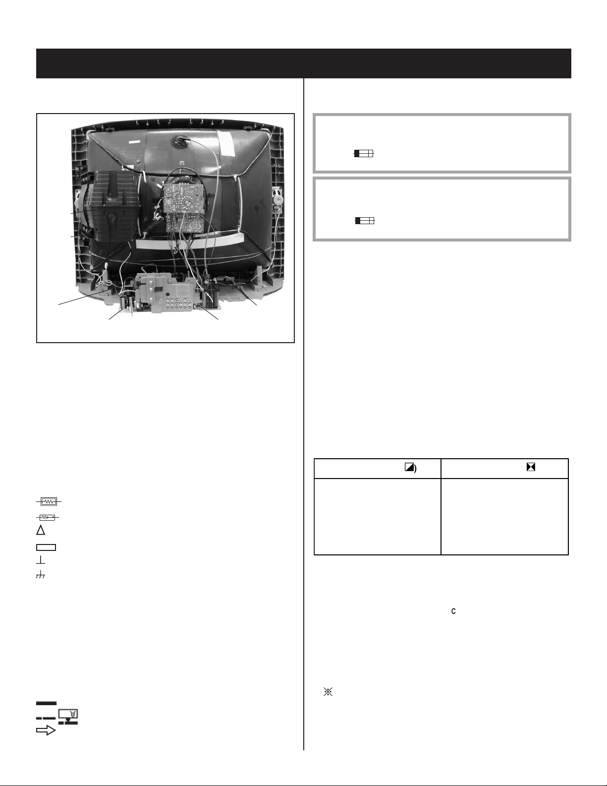
5-1. CIRCUIT BOARDS LOCATION
KV-27FV300/29FV300/32FV300/36FV300
SECTION 5: DIAGRAMS
The components identifi ed by shading and ! symbol are critical for safety. Replace
only with part number specifi ed.
The symbol indicates a fast operating fuse and is displayed on the component
side of the board. Replace only with fuse of the same rating as marked.
C Board
V Board
HR Board
GK Board
A Board
T Board
5-2. PRINTED WIRING BOARDS AND
SCHEMATIC DIAGRAMS INFORMATION
All capacitors are in µF unless otherwise noted. pF : µµF 50WV or less
are not indicated except for electrolytics and tantalums.
All electrolytics are in 50V unless otherwise specifi ed.
All resistors are in ohms. kΩ=1000Ω, MΩ=1000kΩ
Indication of resistance, which does not have one for rating
electrical power, is as follows: Pitch : 5mm
Rating electrical power :
1
/
W in resistance, 1/
4
W and 1/
10
W in chip resistance.
8
: nonfl ammable resistor
: fusible resistor
: internal component
: panel designation and adjustment for repair
: earth ground
: earth-chassis
All variable and adjustable resistors have characteristic curve B, unless
otherwise noted.
Readings are taken with a color-bar signal input.
Readings are taken with a 10MΩ digital multimeter.
Voltages are DC with respect to ground unless otherwise noted.
Voltage variations may be noted due to normal production tolerances.
All voltages are in V.
S : Measurement impossibility.
: B+line
: B-line (Actual measured value may be different).
: signal path (RF)
Circled numbers are waveform references.
1
/
W
4
Les composants identifi es per un trame et une marque
securite. Ne les remplacer que par une piece portant le numero specifi e.
Le symbole indique une fusible a action rapide. Doit etre remplace par une
fusible de meme yaleur, comme maque.
!
sont critiques pour la
The components identifi ed by X in this basic schematic diagram have
been carefully factory-selected for each set in order to satisfy regulations
regarding X-ray radiation. Should replacement be necessary, replace
only with the value originally used.
When replacing components identifi ed by
Y
, make the necessary
adjustments as indicated. If the results do not meet the specifi ed value,
change the component identifi ed by
X
and repeat the adjustment until
the specifi ed value is achieved.
(Refer to R530 and R531 adjustment on page 16.)
When replacing the parts listed in the table below, it is important to
perform the related adjustments.
Part Replaced () Adjustment ()
A BOARD: HV HOLD DOWN
R550, T503, T504, D519,
R530, R531
IC501, R533, D521, R532,
D520, C531, R529, R530,
R531, C532
REFERENCE INFORMATION
RESISTOR
: RN METAL FILM
: RC SOLID
: FPRD NONFLAMMABLE CARBON
: FUSE NONFLAMMABLE FUSIBLE
: RW NONFLAMMABLE WIREWOUND
: RS NONFLAMMABLE METAL OXIDE
: RB NONFLAMMABLE CEMENT
: ADJUSTMENT RESISTOR
COIL
: LF-8L MICRO INDUCTOR
CAPACITOR
: TA TANTALUM
: PS STYROL
: PP POLYPROPYLENE
: PT MYLAR
: MPS METALIZED POLYESTER
: MPP METALIZED POLYPROPYLENE
: ALB BIPOLAR
: ALT HIGH TEMPERATURE
: ALR HIGH RIPPLE
— 29 —
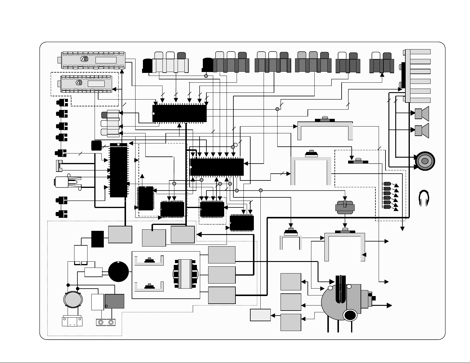
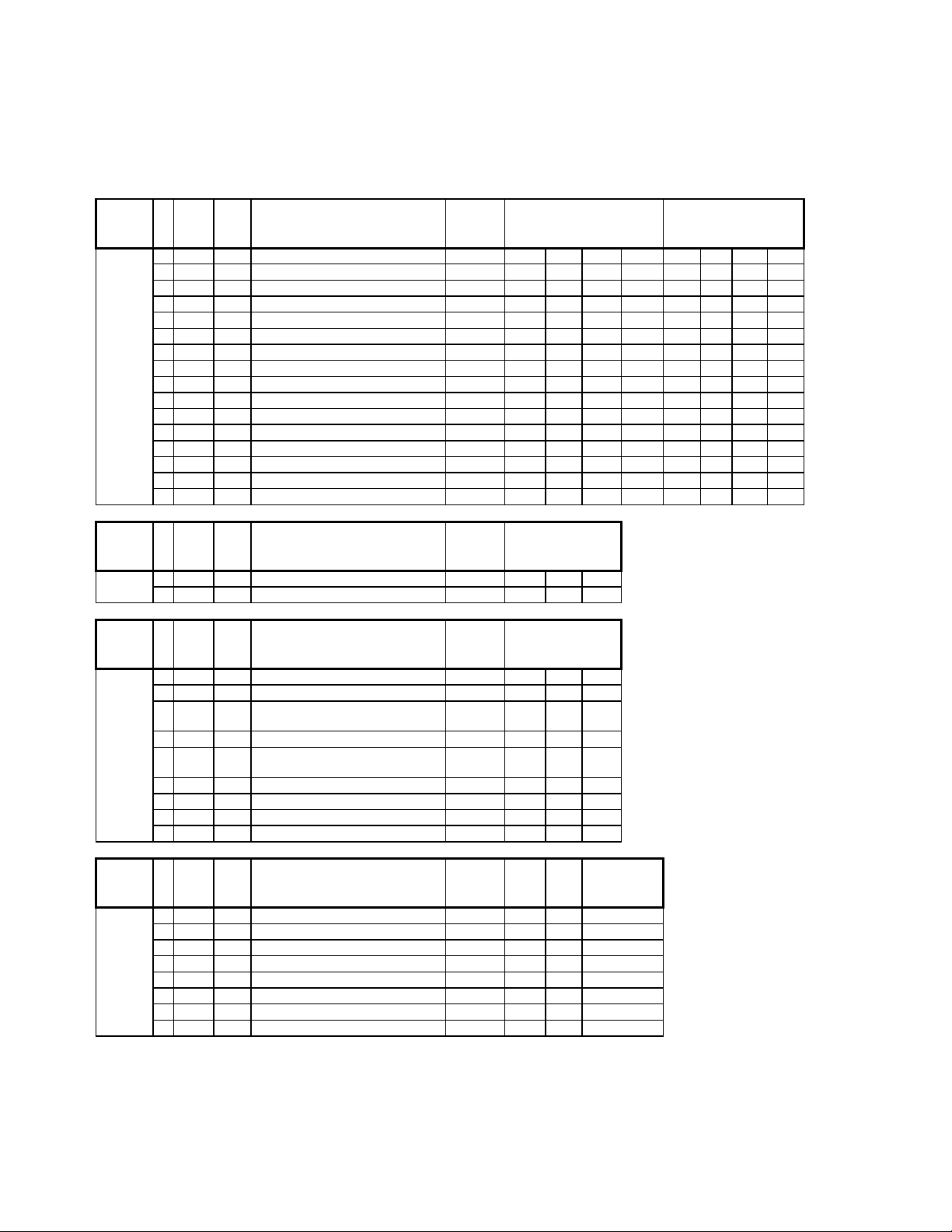
5-3. BLOCK DIAGRAM AND SCHEMATICS
KV-27FV300/29FV300/32FV300/36FV300
Tuner FRONT
Tuner
P board
Sub det-Out
2
L
MOUT
2
2
R
L
V
Mircoprocessor
M306V5ME
I.R.
Det. out
S
REAR
V1 LR
2
2
Audio Processor
NJW1134
I2C Bus
Iprot
(For FV only)
BC board
Y/C
2
2
2
Video processor
CXA2154/5AS
YUV
SRT
TA1226N
5V
Reg.
Yout
Yin
3D comb
MN82832.
9V
Reg.
C
PinP Proc.
M65665FP.
P board
SRT
L.E.D.
Energy Star
G board
Menu
CTRL
5VDC
TV-8
DEC
5V
STBY
S
V2 LR
4
3
B+
Rect.
3
3 RGB
TV-8
2
Y/C
3L comb
TC90A69.
For FS only
135V
REAR
V3 LR
CVBS,FSC
2
2
Vd
V-Out
AN5522 (24-27”)
2
STV9379(32-36”)
Hp
E/W
Pin
Out
2SC4159
YUV AUDIOYUV
Y UV
RGB Driver
TDA6108
LR
Audio Amplifier
TDA8580J
10W&15W
2
IR modulator
BA3308
T board
H.Drive
H-Out
2SD2634(27”)
2SD2645(32-36”)
AUDIO OUT
LR
2
2
3RGB
Emiter
Vert.
Horiz.
To DY
R
L
Speakers
Sub woofer
(for FV only)
IR Head
phones
L.F.T
AC Line
Rect.
Relay
THP
D.G.C.
Power Mosfet
2SK2876
Power Supply
Low B
Rect.
Audio
Rect.
12.5V
24V
— 30 —
OCP
200v
Rect.
+13v
Rect.
-13v
Rect.
G2
FBT
HV
Focus
To CRT
To CRT
FBT
27”-NX4521
32-36”-NX4600
 Loading...