

SONY KV-21SE40A Service Manual

HISTORY INFORMATION FOR THE FOLLOWING MANUAL:
SERVICE MANUAL
MODEL NAME REMOTE COMMANDER DESTINATION CHASSIS NO.
KV-27FS100L
KV-27FS100L
KV-29FS100L
KV-29FS100L
RM-Y180 US SCC-S61G-A
RM-Y180 CANADA SCC-S59G-A
RM-Y180 LATIN NORTH SCC-S60R-A
RM-Y180 LATIN SOUTH SCC-S60S-A
BA-6
CHASSIS
ORIGINAL MANUAL ISSUE DATE: 7/2003
:UPDATED ITEM
☛
REVISION DATE SUBJECT
7/2003 No revisions or updates are applicable at this time.
11/2003 Replaced A Board Schematic to correct T603 PIN Connection (Replace Page 31)
TRINITRON® COLOR TELEVISION
9-965-948-02
Self Diagnosis
Supported model
SERVICE MANUAL
MODEL NAME REMOTE COMMANDER DESTINATION CHASSIS NO.
KV-27FS100L
KV-27FS100L
KV-29FS100L
KV-29FS100L
RM-Y180 US SCC-S61G-A
RM-Y180 CANADA SCC-S59G-A
RM-Y180 LATIN NORTH SCC-S60R-A
RM-Y180 LATIN SOUTH SCC-S60S-A
BA-6
CHASSIS
9-965-948-02
KV-27FS100L RM-Y180
TRINITRON® COLOR TELEVISION

KV-27FS100L/29FS100L
TABLE OF CONTENTS
SECTION TITLE PAGE
Specications ............................................................................................................................................................................. 4
Warnings and Cautions .............................................................................................................................................................. 5
Safety Check-Out ....................................................................................................................................................................... 6
Self-Diagnostic Function............................................................................................................................................................. 7
SECTION 1: DISASSEMBLY............................................................................................................................................................. 9
1-1. Rear Cover Removal.......................................................................................................................................................... 9
1-2. Chassis Assembly Removal............................................................................................................................................... 9
1-3. Service Position ................................................................................................................................................................. 9
1-4. Picture Tube Removal...................................................................................................................................................... 10
Anode Cap Removal Procedure....................................................................................................................................... 10
SECTION 2: SET-UP ADJUSTMENTS.............................................................................................................................................11
2-1. Beam Landing ...................................................................................................................................................................11
2-2. Convergence .................................................................................................................................................................... 12
2-3. Focus ............................................................................................................................................................................... 13
2-4. Screen (G2)...................................................................................................................................................................... 14
2-5. Method of Setting the Service Adjustment Mode ............................................................................................................. 14
2-6. White Balance Adjustments ............................................................................................................................................. 14
SECTION 3: SAFETY RELATED ADJUSTMENTS......................................................................................................................... 15
3-1. X R564 Conrmation Method (HV Hold-Down Conrmation) and Readjustments ........................................................ 15
3-2. B+ Voltage Conrmation and Adjustment ........................................................................................................................ 15
SECTION 4: CIRCUIT ADJUSTMENTS.......................................................................................................................................... 17
4-1. Setting the Service Adjustment Mode .............................................................................................................................. 17
4-2. Memory Write Conrmation Method ................................................................................................................................ 17
4-3. Remote Adjustment Buttons and IndicatorS .................................................................................................................... 17
4-4. ID Map Table.................................................................................................................................................................... 26
4-5. A Board Adjustments........................................................................................................................................................ 26
SECTION 5: DIAGRAMS................................................................................................................................................................. 29
5-1. Circuit Boards Location .................................................................................................................................................... 29
5-2. Printed Wiring Board and Schematic Diagram Information.............................................................................................. 29
5.3. Block Diagram and Schematics......................................................................................................................................... 30
A Board Schematic Diagram ........................................................................................................................................... 31
V Board Schematic Diagram ............................................................................................................................................ 35
HS Board Schematic Diagram ......................................................................................................................................... 37
CV Board Schematic Diagram ......................................................................................................................................... 39
D Board Schematic Diagram............................................................................................................................................ 41
5-4. Semiconductors ............................................................................................................................................................... 43
SECTION 6: EXPLODED VIEWS................................................................................................................................................... 44
6-1. Chassis ............................................................................................................................................................................. 44
6-2. Picture Tube ..................................................................................................................................................................... 45
SECTION 7: ELECTRICAL PARTS LIST....................................................................................................................................... 46
— 3 —
SPECIFICATIONS
KV-27FS100L
KV-29FS100L
Power requirements (Latin North) 120V, 60Hz
Power requirements (Latin South) 220V, 50/60Hz
Number of Inputs/Outputs
Video
1)
3
S Video
2)
1
Y, P
B
, P
R
3)
1
Audio
4)
2
Speaker output (W) 10 W x 2
Power Consumption (W)
In use (Max) 180W
In Standby 1W
Dimensions(W/H/D)
mm 770 x 590 x 490 mm
in
30
1/4
x 23
1/4
x 19
1/4
Mass
kg 45.5 kg
lbs
100 lbs. 5 oz.
KV-27FS100L/29FS100L
Television system
American TV Standard, NTSC
Channel coverage
VHF: 2-13/ UHF: 14-69/ CATV: 1-125
Picture tube
FD Trinitron® tube
Visible screen size
27 inch picture measured diagonally
Actual screen size
29 inch measured diagonally
— 4 —
1)
1 Vp-p 75 ohms unbalanced, sync negative
2)
Y: 1 Vp-p 75 ohms unbalanced, sync negative
C: 0.286 Vp-p (Burst signal), 75 ohms
3) Y: 1.0 Vp-p, 75 ohms, sync negative; PB: 0.7 Vp-p, 75 ohms;
PR Vp-p, 75 ohms.
4)
500 mVrms (100% modulation), Impedance: 47 kilohms
5)
More than 408 mVrms at the maximum volume setting (variable)
More than 408 mVrms (x); Impedance (output): 2 kilohms
Antenna
75 ohm external terminal for VHF/UHF
Supplied Accessories
Remote Commander:
RM-Y180
Size AA (R6) batteries (2)
Antenna, Telescopic
(•) SRS (SOUND RETRIEVAL SYSTEM)
The (•) SRS (SOUND RETRIEVAL SYSTEM) is manufactured by
Sony Corporation under license from SRS Labs, Inc. It is covered by U.S.
Patent No. 4,748,669. Other U.S. and foreign patents pending.
The word ‘SRS’ and the SRS symbol (•) are registered trademarks of
SRS Labs, Inc. BBE and BBE symbol are trademarks of BBE Sound, Inc.
and are licensed by BBE Sound, Inc. under U.S. Patent No. 4,638,258.
Design and specications are subject to change without notice.

KV-27FS100L/29FS100L
WARNINGS AND CAUTIONS
CAUTION
Short circuit the anode of the picture tube and the anode cap to the metal chassis, CRT shield, or carbon painted on the CRT, after
removing the anode.
WARNING!!
An isolation transformer should be used during any service to avoid possible shock hazard, because of live chassis. The chassis of
this receiver is directly connected to the AC power line.
! SAFETY-RELATED COMPONENT WARNING!!
Components identied by shading and ! mark on the schematic diagrams, exploded views, and in the parts list are critical for safe
operation. Replace these components with Sony parts whose part numbers appear as shown in this manual or in supplements
published by Sony. Circuit adjustments that are critical for safe operation are identied in this manual. Follow these procedures
whenever critical components are replaced or improper operation is suspected.
ATTENTION!!
Apres avoir deconnecte le cap de l’anode, court-circuiter l’anode du tube cathodique et celui de l’anode du cap au chassis metallique
de l’appareil, ou la couche de carbone peinte sur le tube cathodique ou au blindage du tube cathodique.
An d’eviter tout risque d’electrocution provenant d’un chássis sous tension, un transformateur d’isolement doit etre utilisé lors de tout
dépannage. Le chássis de ce récepteur est directement raccordé à l’alimentation du secteur.
! ATTENTION AUX COMPOSANTS RELATIFS A LA SECURITE!!
Les composants identies par une trame et par une marque ! sur les schemas de principe, les vues explosees et les listes de pieces
sont d’une importance critique pour la securite du fonctionnement. Ne les remplacer que par des composants Sony dont le numero
de piece est indique dans le present manuel ou dans des supplements publies par Sony. Les reglages de circuit dont l’importance
est critique pour la securite du fonctionnement sont identies dans le present manuel. Suivre ces procedures lors de chaque
remplacement de composants critiques, ou lorsqu’un mauvais fonctionnement suspecte.
— 5 —
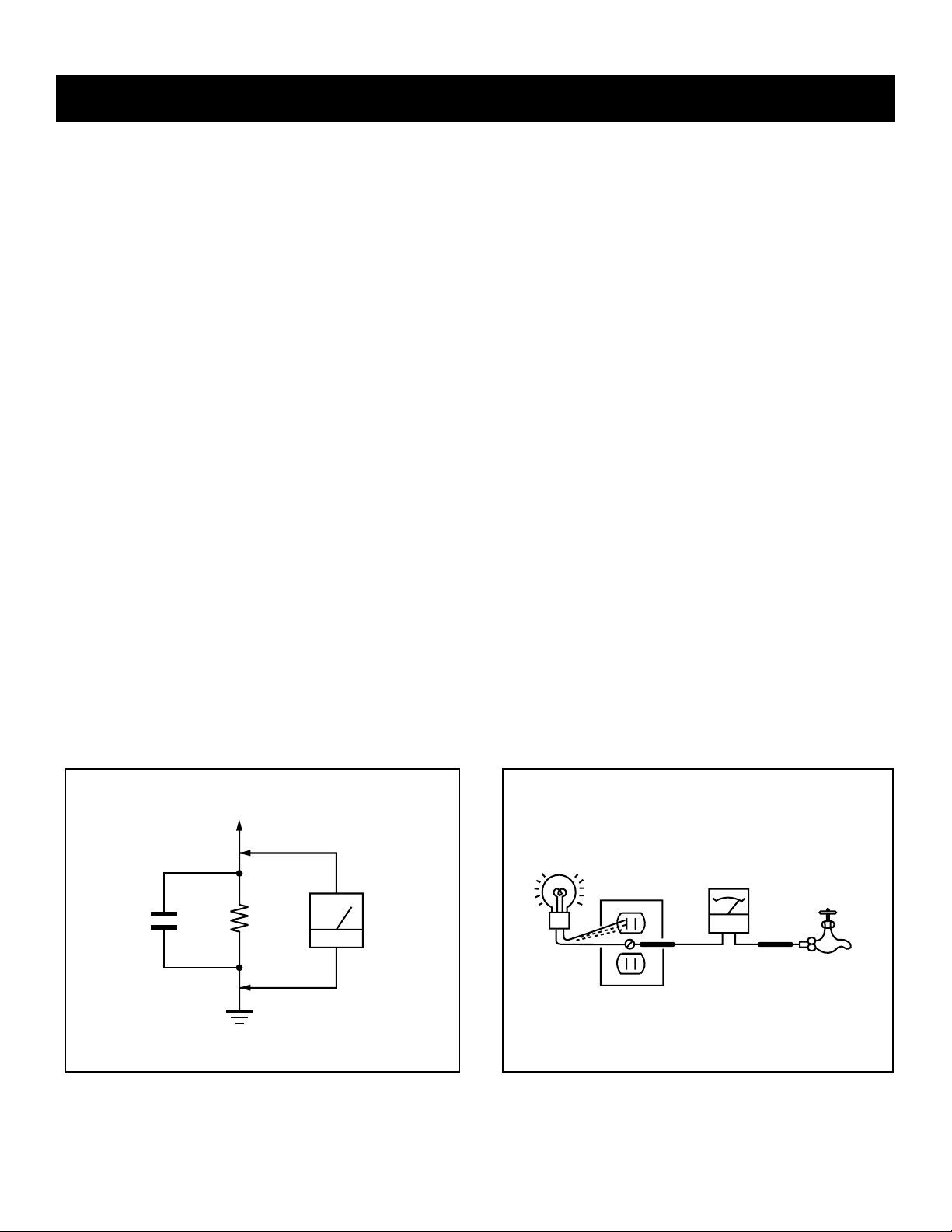
SAFETY CHECK-OUT
To Exposed Metal
Parts on Set
0.15 F
1.5 K Ω
AC
Voltmeter
(0.75 V)
Earth Ground
Trouble Light
AC Outlet Box
Ohmmeter
Cold-water Pipe
KV-27FS100L/29FS100L
After correcting the original service problem, perform the following
safety checks before releasing the set to the customer:
1. Check the area of your repair for unsoldered or poorly soldered
connections. Check the entire board surface for solder splashes and
bridges.
2. Check the interboard wiring to ensure that no wires are “pinched” or
touching high-wattage resistors.
3. Check that all control knobs, shields, covers, ground straps, and
mounting hardware have been replaced. Be absolutely certain that
you have replaced all the insulators.
4. Look for unauthorized replacement parts, particularly transistors,
that were installed during a previous repair. Point them out to the
customer and recommend their replacement.
5. Look for parts which, though functioning, show obvious signs of
deterioration. Point them out to the customer and recommend their
replacement.
6. Check the line cords for cracks and abrasion. Recommend the
replacement of any such line cord to the customer.
7. Check the B+ and HV to see if they are specied values. Make sure
your instruments are accurate; be suspicious of your HV meter if sets
always have low HV.
8. Check the antenna terminals, metal trim, “metallized” knobs, screws,
and all other exposed metal parts for AC leakage. Check leakage as
described below.
Leakage Test
The AC leakage from any exposed metal part to earth ground and
from all exposed metal parts to any exposed metal part having a
return to chassis, must not exceed 0.5 mA (500 microamperes).
Leakage current can be measured by any one of three methods.
1. A commercial leakage tester, such as the Simpson 229 or RCA
WT-540A. Follow the manufacturers’ instructions to use these
instructions.
2. A battery-operated AC milliampmeter. The Data Precision 245
digital multimeter is suitable for this job.
3. Measuring the voltage drop across a resistor by means of a VOM
or battery-operated AC voltmeter. The “limit” indication is 0.75
V, so analog meters must have an accurate low voltage scale.
The Simpson’s 250 and Sanwa SH-63TRD are examples of
passive VOMs that are suitable. Nearly all battery-operated digital
multimeters that have a 2 VAC range are suitable (see Figure A).
How to Find a Good Earth Ground
A cold-water pipe is a guaranteed earth ground; the cover-plate
retaining screw on most AC outlet boxes is also at earth ground. If the
retaining screw is to be used as your earth ground, verify that it is at
ground by measuring the resistance between it and a cold-water pipe
with an ohmmeter. The reading should be zero ohms.
If a cold-water pipe is not accessible, connect a 60- to 100-watt
trouble- light (not a neon lamp) between the hot side of the receptacle
and the retaining screw. Try both slots, if necessary, to locate the hot
side on the line; the lamp should light at normal brilliance if the screw
is at ground potential (see Figure B).
Figure A. Using an AC voltmeter to check AC leakage. Figure B. Checking for earth ground.
— 6 —
KV-27FS100L/29FS100L
Self Diagnosis
Supported model
2 times
4 times
5 times
LED ON 0.3 sec.
LED OFF 0.3 sec.
LED OFF
3 sec.
SELF-DIAGNOSTIC FUNCTION
The units in this manual contain a self-diagnostic function. If an error occurs, the STANDBY/TIMER LED will automatically begin to ash. The number
of times the LED ashes translates to a probable source of the problem. A denition of the STANDBY/TIMER LED ash indicators is listed in the
instruction manual for the user’s knowledge and reference. If an error symptom cannot be reproduced, the Remote Commander can be used to review
the failure occurrence data stored in memory to reveal past problems and how often these problems occur.
Diagnostic Test Indicators
When an error occurs, the STANDBY/TIMER LED will ash a set number of times to indicate the possible cause of the problem. If there is more than
one error, the LED will identify the rst of the problem areas.
Results for all of the following diagnostic items are displayed on screen. No error has occurred if the screen displays a “0”.
Diagnostic Item
Description
Power does not turn on
+B overcurrent (OCP)*
I-Prot
IK (AKB)
No. of times
STANDBY/ TIMER
lamp ashes
Does not light
2 times
4 times
5 times
Self-Diagnositc
Display/
Diagnostic Result
2:0 or 2:1
4:0 or 4:1
5:0 or 5:1
Probable Cause Location
• Power cord is not plugged in.
• Fuse is burned out (F601). (A Board)
• H.OUT (Q505) is shorted. (A Board)
• IC1751 is shorted. (CV Board)
• +13V is not supplied. (A Board)
• IC545 is faulty. (A Board)
• IC001 is faulty. (A Board)
• Screen (G2) is improperly adjusted.**
Detected Symptoms
• Power does not come on.
• No power is supplied to the TV.
• AC Power supply is faulty.
• Power does not come on.
• Load on power line is shorted.
• Has entered standby state after horizontal raster.
• Vertical deection pulse is stopped.
• Power line is shorted or power supply is stopped.
• No raster is generated.
• CRT Cathode current detection reference pulse
output is small.
*If a +B overcurrent is detected, stoppage of the vertical deection is detected simultaneously. The symptom that is diagnosed rst by the
mircrocontroller is displayed on the screen.
**Refer to Screen (G2) Adjustments in Section 2-4. of this manual.
Display of Standby/Timer LED Flash Count
Diagnostic Item Flash Count*
+B Overcurrent 2 times
I-Prot 4 times
IK (AKB) 5 times
*One ash count is not used for self-diagnostic.
Stopping the Standby/Timer LED Flash
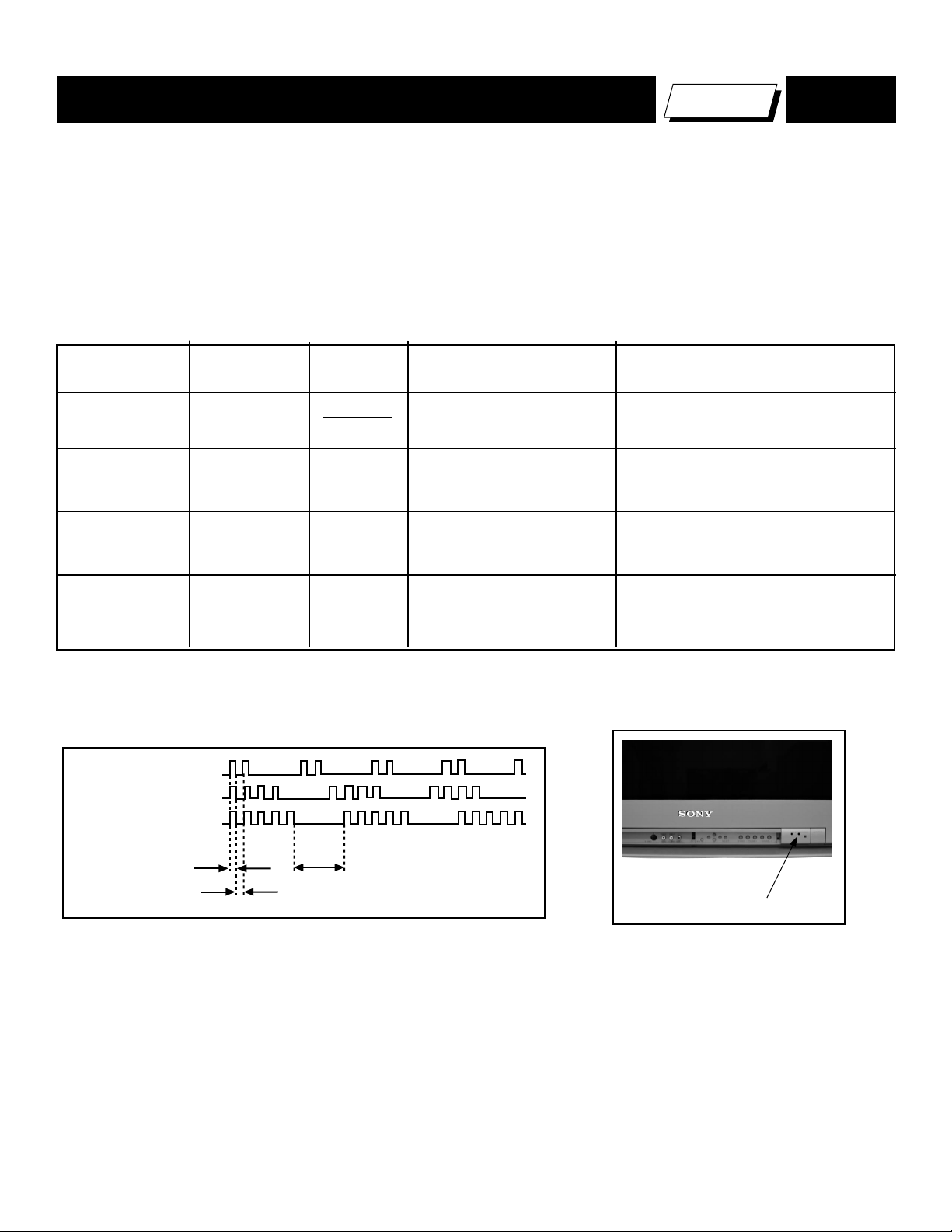
Turn off the power switch on the TV main unit or unplug the power cord from the outlet to stop the STANDBY/TIMER LAMP from ashing.
Standby/Timer LED
— 7 —
KV-27FS100L/29FS100L
A BOARD
IC001
Y/CHROMA JUNGLE
A
BOARD
IC545
V.
OUT
A
BOARD
IC001
SYSTEM
A
BOARD
IC002
MEMORY
IK-AKBIN
FROM
CV BOARD
IC1751 PIN 5
I-HLDWN
FROM
A BOARD
IC561
PIN 7
72
O-LED
REF
I-Prot
IO-BDAT
BDA
DISPLAY
51
3
78
79
53
5
Self-Diagnostic Screen Display
For errors with symptoms such as “power sometimes shuts off” or “screen sometimes goes out” that cannot be conrmed, it is possible to bring up past
occurrences of failure on the screen for conrmation.
To Bring Up Screen Test
In standby mode, press buttons on the Remote Commander sequentially, in rapid succession, as shown below:
Display
Self-Diagnostic Screen Display
Handling of Self-Diagnostic Screen Display
Since the diagnostic results displayed on the screen are not automatically cleared, always check the self-diagnostic screen during repairs. When you
have completed the repairs, clear the result display to “0”.
Unless the result display is cleared to “0”, the self-diagnostic function will not be able to detect subsequent faults after completion of the repairs.
Clearing the Result Display
To clear the result display to “0”, press buttons on the Remote Commander sequentially when the diagnostic screen is displayed, as shown below:
Channel 8
Quitting the Self-Diagnostic Screen
To quit the entire self-diagnostic screen, turn off the power switch on the Remote Commander or the main unit.
Channel
SELF DIAGNOSTIC
2: 000
3: N/A
4: 000
5: 001
101: N/A
ENTER
5
Sound Volume - Power ON
Note that this differs from entering the Service Mode (Sound Volume + ).
Numeral “0” means that no fault was detected.
Numeral “1” means a fault was detected one time only.
Self-Diagnostic Circuit
+B overcurrent (OCP)
Occurs when an overcurrent on the +B (135V) line is detected by pin 72 of IC001 (A Board). If the voltage of pin 72 of IC001 (A Board) is less than 1V
when V.SYNC is more than seven verticals in a period, the unit will automatically turn off.
I-Prot
Occurs when an absence of the vertical deection pulse is detected by pin 78 of IC001 (A Board). Power supply will shut down when waveform interval
exceeds 2 seconds.
IK (AKB)
If the RGB levels* do not balance within 2 seconds after the power is turned on, this error will be detected by IC001 (A Board). TV will stay on, but
there will be no picture.
*(Refers to the RGB levels of the AKB detection Ref pulse that detects 1K).
— 8 —
1-1. REAR COVER REMOVAL
1
2
Rear Cover
Screws +BVTP 4X16 TYPE2 TT(B)
2
SECTION 1: DISASSEMBLY
Screws +BVTP 4X16 TYPE2 TT(B)
4
KV-27FS100L/29FS100L
Screws +BVTP 4X16 TYPE2 TT(B)
2
Screws +BVTP 4X16 TYPE2 TT(B)
2
Screws +BVTP 3X12 TYPE2 TT(B)
5
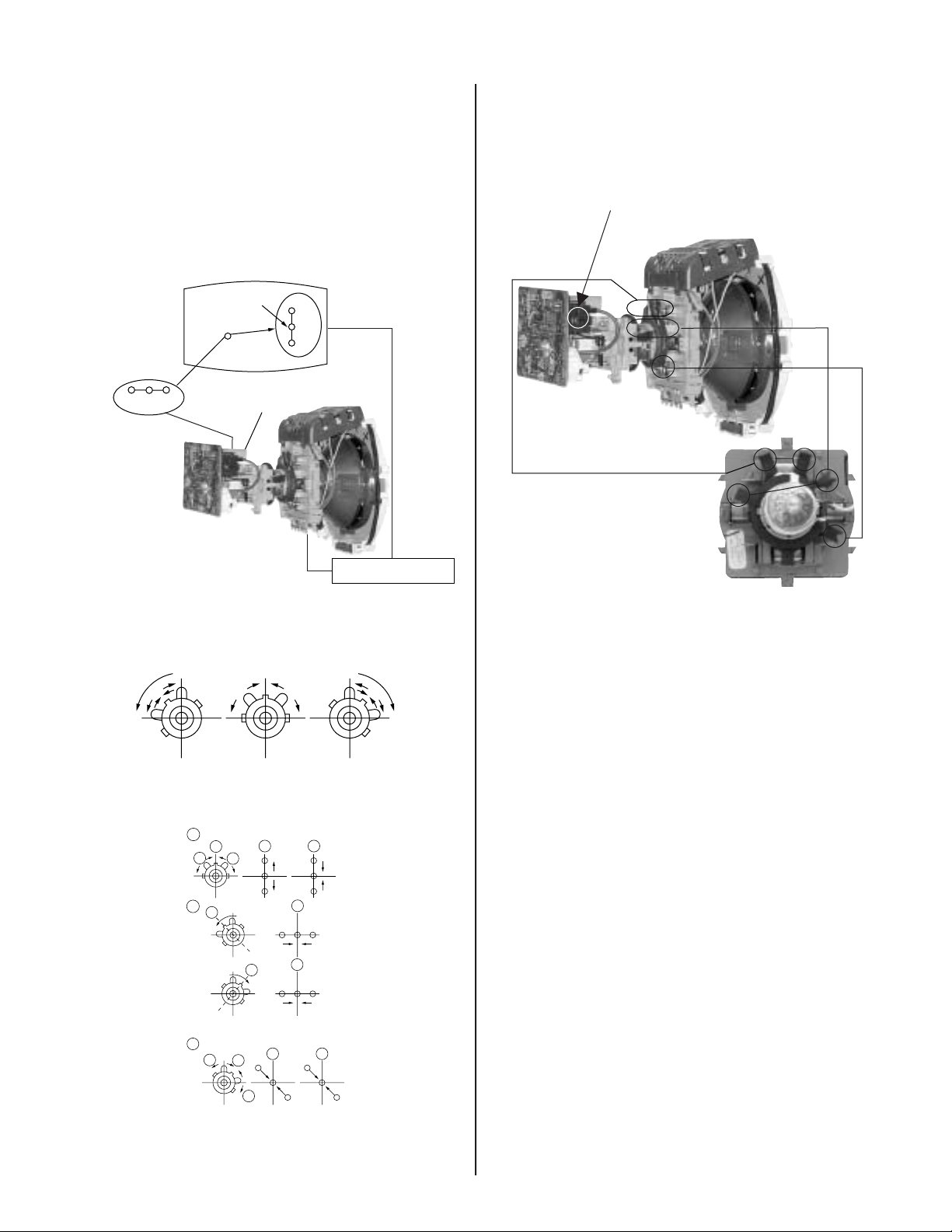
1-2. CHASSIS ASSEMBLY REMOVAL 1-3. SERVICE POSITION
V Board
Claw
Chassis Assembly
CV Board
HS Board
A Board
D Board
Press on catch tab to release A Board.
Disconnect cables as needed to allow A Board to be removed.
— 9 —
1-4. PICTURE TUBE REMOVAL
WARNING: BEFORE REMOVING THE ANODE CAP
High voltage remains in the CRT even after the power is disconnected. To avoid electric shock,
discharge CRT before attempting to remove the anode cap. Short between anode and CRT
coated earth ground strap.
1
10
1. Discharge the anode of the CRT and remove the anode cap.
8
7
3
6
2
5
9
4
2. Unplug all interconnecting leads from the deection yoke, neck
assembly, degaussing coils and CRT grounding strap.
3. Remove the CV Board from the CRT.
4. Remove the chassis assembly.
5. Loosen the neck assembly xing screw and remove.
6. Loosen the deection yoke xing screw and remove.
7. Place the set with the CRT face down on a cushion and remove
the degaussing coil holders.
8. Remove the degaussing coils.
9. Remove the CRT grounding strap and spring tension devices.
10. Unscrew the four CRT xing screws [located on each CRT
corner] and remove the CRT [Take care not to handle the CRT
by the neck].
KV-27FS100L/29FS100L
ANODE CAP REMOVAL PROCEDURE
WARNING: High voltage remains in the CRT even after the power is disconnected. To avoid electric shock, discharge CRT before attempting to
remove the anode cap. Short between anode and coated earth ground strap of CRT.
NOTE: After removing the anode cap, short circuit the anode of the picture tube and the anode cap to either the metal chassis, CRT shield, or carbon
painted on the CRT.
REMOVAL PROCEDURES
Turn up one side of the rubber cap in
the direction indicated by arrow a .
HOW TO HANDLE AN ANODE CAP
1. Do not use sharp objects which may cause damage to the surface of the anode
cap.
2. To avoid damaging the anode cap, do not squeeze the rubber covering too
hard. A material tting called a shatter-hook terminal is built into the rubber.
3. Do not force turn the foot of the rubber cover. This may cause the shatter-hook
terminal to protrude and damage the rubber.
Use your thumb to pull the rubber
cap rmly in the direction indicated
by arrow b .
When one side of the rubber cap separates from
the anode button, the anode cap can be removed
by turning the rubber cap and pulling it in the
direction of arrow c .
— 10 —
SECTION 2: SET-UP ADJUSTMENTS
Purity Control
a
c
b
d
b
a
c d
Purity control
corrects this area.
Disk magnets
or rotatable disk
magnets correct
these areas (a-d).
Deflection yoke positioning
corrects these areas.
KV-27FS100L/29FS100L
The following adjustments should be made when a complete
realignment is required or a new picture tube is installed.
These adjustments should be performed with rated power supply
voltage unless otherwise noted.
Set the controls as follows unless otherwise noted:
VIDEO MODE: Standard
PICTURE CONTROL: Normal
BRIGHTNESS CONTROL: Normal
2-1. BEAM LANDING
Before beginning adjustment procedure:
1. Degauss the entire screen.
2. Feed in the white pattern signal.
ADJUSTMENT PROCEDURE
1. Input a raster signal with the pattern generator.
2. Loosen the deection yoke mounting screw, and set the purity
control to the center as shown below:
Perform the adjustments in order as follows:
1. Beam Landing
2. Convergence
3. Focus
4. Screen (G2)
5. White Balance
Note Test Equipment Required:
1. Color Bar Pattern Generator
2. Degausser
3. DC Power Supply
4. Digital Multimeter
6. Switch over the raster signal to red and blue and conrm the
condition.
7. When the position of the deection yoke is determined, tighten it with
the deection yoke mounting screw.
8. If landing at the corner is not right, adjust by using the disk magnets.
3. Turn the raster signal of the pattern generator to green.
4. Move the deection yoke backward, and adjust with the purity control
so that green is in the center and red and blue are even on both
sides.
5. Move the deection yoke forward, and adjust so that the entire
screen becomes green.
— 11 —
KV-27FS100L/29FS100L
2-2. CONVERGENCE
Before starting convergence adjustments:
1 Perform FOCUS, VLIN and VSIZE adjustments.
2. Set BRIGHTNESS control to minimum.
3. Feed in dot pattern.
VERTICAL STATIC CONVERGENCE
1. Adjust V. STAT magnet to converge red, green and blue dots in the
center of the screen.
Center dot
RV1750
R
B
G
H.STAT
R
G
B
HORIZONTAL STATIC CONVERGENCE
If the blue dot does not converge with the red and green dots, perform
the following:
1. Move H STAT VR magnet (a) to correct insufÞ cient H.Static
convergence.
H STAT VR
V. STAT
BMC MAGNET
PURITY
V.STAT magnet
2. Tilt the V. STAT magnet and adjust static convergence to open or
close the V. STAT magnet.
When the V. STAT magnet is moved in the direction of arrow a and b,
red, green, and blue dots move as shown below:
1
a
b
2
a
a
b
B
G
R
b
b
B
G
R
a
RGB
b
BGR
3
b
a
a
R
G
b
b
B
G
B
R
— 12 —
DYNAMIC CONVERGENCE ADJUSTMENT
B G R
G B
R
G
B
R
R
R
G
B
G
B
G
B
R
BGR
G
B
G
B
R
R
G
B
G
G
B
R
B
R
R
(TLV)
YCH
XCV
TLV
CV
Board
RV1750
V
.STAT
TLH Plate
B R R B
(R)(B) (B)(R)
TLH+
TLH-
ba
c
d
a
b
d
a-d: screen-corner
misconvergence
c
Before performing this adjustment, perform Horizontal and Vertical Static
Convergence Adjustment.
1. Slightly loosen deection yoke screw.
2. Remove deection yoke spacers.
3. Move the deection yoke for best convergence as
shown below:
KV-27FS100L/29FS100L
4. Adjust XCV core to balance X axis.
5. Adjust YCH VR to balance Y axis.
6. Adjust vertical red and blue convergence with V.TILT (TLV VR.)
Note: Perform adjustment 3-6 while tracking items 1 and 2.
SCREEN-CORNER CONVERGENCE
1. Afx a permalloy assembly corresponding to the misconverged areas:
4. Tighten the deection yoke screw.
5. Install the deection yoke spacers.
TLH PLATE ADJUSTMENT
1. Input crosshatch pattern.
2. Adjust PICTURE QUALITY to standard, PICTURE and BRIGHTNESS
to 50%, and OTHER to standard.
3 Adjust the Horizontal Convergence of red and blue dots by tilting the
TLH plate on the deection yoke.
2-3. FOCUS
1. Adjust FOCUS control for best pictures.
Focus (FV)
Screen (G2)
— 13 —
KV-27FS100L/29FS100L
Pedestal
160 – 2VDC
Ground
Mode
Category
Display
Item
Display
Item
Signal
Type
ntsc
service
defl
vchp
00000000
00000000
hsiz 16
service defl hsiz 16
ntsc
vchp 00000000 00000000
Category
Display
Item
Mode
Item
Data
Signal
Type
write
ENTER
Green
Red
MUTING
2-4. SCREEN (G2)
1. Input a dot pattern.
2. Set the PICTURE and BRIGHTNESS controls at minimum and
COLOR control at normal.
3. Adjust SBRT, GCUT, BCUT in service mode with an oscilloscope as
shown below so that voltages on the red, green, and blue cathodes
are 160 ± 2VDC.
±
4. Observe the screen and adjust SCREEN (G2) VR in FBT to obtain
the faintly visible background of dot signal.
2-5. METHOD OF SETTING THE SERVICE ADJUSTMENT MODE
SERVICE MODE PROCEDURE
1. Standby mode (power off).
2. Press
Display
Channel 5
Sound Volume +
Power
on the Remote Commander (press each button within a second).
2-6. WHITE BALANCE ADJUSTMENTS
1. Input an entire white signal with burst.
2. Set to Service Adjustment Mode.
3. Set the PICTURE and BRIGHTNESS to minimum.
4. Adjust with SBRT if necessary.
4
5. Select GCUT and BCUT with
6
6. Adjust with
3
for the best white balance.
and
1
7. Set the PICTURE and BRIGHTNESS to maximum.
8. Select GDRV and BDRV with
6
9. Adjust with
3
10. To write into memory, press
for the best white balance.
and
MUTING
and
1
and
.
4
.
then
ENTER
.
SERVICE ADJUSTMENT MODE ON
1. The CRT displays the time being adjusted.
4
1
on the Remote Commander to select the time.
2. Press
3. Press
4. Press
or
6
3
on the Remote Commander to change the data.
or
ENTER
MUTING
then
to save into the memory.
SERVICE ADJUSTMENT MODE MEMORY
Turn the set off then on to exit Service Adjustment Mode.
— 14 —
SECTION 3: SAFETY RELATED ADJUSTMENTS
KV-27FS100L/29FS100L
3-1. X R564 CONFIRMATION METHOD (HV HOLD-DOWN CONFIRMATION) AND READJUSTMENTS
The following adjustments should always be performed when replacing
the following components which are marked with
diagram:
Part Replaced ( )
Y
DY, T585, CRT, IC001, IC561,
IC600, IC604, C506,C507,C508,
Y
on the schematic
Adjustment ( )
HV HOLD-DOWN
R564
HOLD-DOWN READJUSTMENT
If the setting indicated in Step 2 of Hold-Down Operation Confi rmation
cannot be met, readjustment should be performed by altering the
resistance value of R564 component marked with
C510, C511, C513, C514, L588,
D565, D566, D567,PH602,R564,
R585, R588,R628, R851,T510,
T511....................A Board
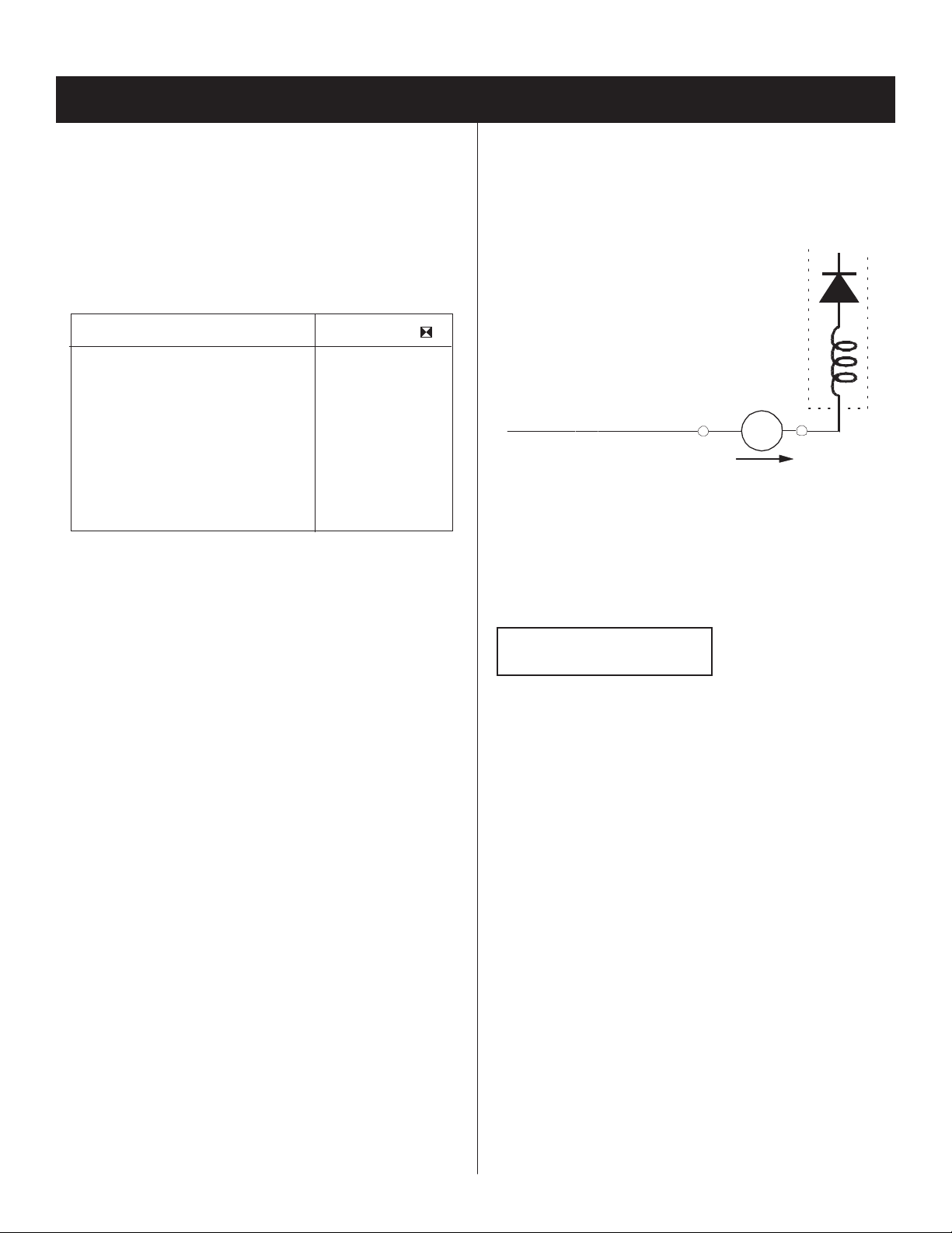
3-2. B+ VOLTAGE CONFIRMATION AND ADJUSTMENT
PREPARATION BEFORE CONFIRMATION
1. Using a Variac, apply AC input voltage: 120 ±2 VAC.
2. Turn the POWER switch ON.
3. Input a white signal and set the PICTURE and BRIGHTNESS
controls to maximum.
4. Confi rm that the voltage between C566 (+) or TP30 and ground is
more than 105 VDC.
HOLD-DOWN OPERATION CONFIRMATION
1. Connect the current meter between Pin 11 of the FBT (T585) and the
PWB land where Pin 11 would normally attach (See Figure 1 on the
next page).
2. Input a dot signal and set PICTURE and BRIGHTNESS to minimum:
IABL = 100 ± 100µA.
3. Confi rm the voltage of A Board TP-23 is 138.0 ± 0.3VDC.
4. Connect the digital voltmeter and the DC power supply via Diode
1SS119 to C566 (+) and ground (See Figure 1 on next page).
5. Increase the DC power voltage gradually until the picture blanks out.
6. Turn DC power source off immediately.
7. Read the digital voltmeter indication (standard < 117VDC).
8. Input a white signal and set PICTURE and BRIGHTNESS to
maximum: IABL = 1650 ± 100µA.
9. Repeat steps 4 to 7.
Note: The following adjustments should always be performed when
replacing the following components, which are marked with
schematic diagram on the A Board:
1. Using a Variac, apply AC input voltage: 130 + 2.0 / - 0.0 VAC.
2. Input a DOT pattern at Q.C.
3. Set the PICTURE and the BRIGHTNESS controls to minimum.
4. Confi rm the voltage of A Board between TP-23 & Ground is <136.6
5. If step 4 is not satisfi ed, replace the components listed above, then
ABL
A BOARD: Y IC604, PH602
VDC.
repeat Steps 1 – 3.
T585
FBT
amPmeter
3.0 mA DC
range
+
A
IABL
X
.
-
Y
on the
— 15 —
KV-27FS100L/29FS100L
Q59
0
T50
5
6
0
2
R
505
C62
4
C50
5
C50
6
D59
8
C58
2
L
588
Q52
2
IC565
IC400
Q65
0
IC402
IC545
IC561
L51
3
L51
1
HS522
C52
5
L52
5
D
5
2
6
C51
3
D00
6
L
5
1
6
C51
4
D54
5
D56
6
D52
5
L
008
L58
2
C
526
C
5
1
1
Q00
4
Q
0
0
5
IC005
C
5
1
2
C
6
1
8
CN5
1
5
IC401
R49
4
R20
0
R
487
R46
1
R45
5
R45
8
R48
5
R10
6
R04
1
R04
0
R41
6
R
2
2
7
R20
3
R57
4
R52
8
R52
9
R53
7
R55
7
R54
9
R53
3
R
534
R40
0
R08
6
R08
0
R
085
C54
8
C52
9
Q40
4
Q30
6
Q40
2
Q
4
0
0
Q40
1
Q
4
0
3
C20
2
JR1
C53
0
C
5
4
0
C45
4
C05
2
C05
3
R52
6
R32
3
R59
3
R50
6
R57
0
R
5
6
9
R56
8
R54
7
R50
2
R58
9
R
411
R40
8
R21
1
R21
2
R59
4
R58
3
R54
6
C45
3
C49
8
C46
0
C41
5
C42
0
C42
2
C56
1
C
2
1
2
C
2
0
6
C20
7
C
4
2
4
C
0
5
1
C66
1
C66
0
C
451
C57
1
D20
1
D23
2
D23
5
D20
4
D20
5
D
5
6
8
D63
0
D56
9
D52
8
D
5
6
7
R
0
3
0
R20
9
R54
0
R54
1
R20
8
R56
6
D56
2
R53
2
R51
1
C64
0
C61
0
4
0
2
C
5
9
5
C54
5
C54
7
R
5
0
4
C54
4
C56
2
D22
0
L00
9
C52
8
C52
7
R58
1
C50
4
C
5
0
2
601
L51
5
R51
0
R
588
R51
5
R30
7
R20
2
R22
9
R22
2
D62
4
Q
5
0
5
Q50
6
C
0
6
9
R51
2
R51
4
R90
1
R54
8
R90
2
C
N20
1
625
T51
1
PS401
L
3
7
1
L37
0
JR1
2
JR505
D41
4
C65
1
C45
0
R50
3
R59
1
C59
0
R60
9
C59
7
T58
5
R43
7
R57
1
R59
8
Q52
1
R57
5
C51
0
D50
6
C36
0
R36
1
R23
3
J20
6
J20
2
R25
0
E
B
E
B
6
4
1
3
HDY
-
HDY
-
HDY
+
HDY
+
VDY
-
VDY
+
H-OUT
N/C
200
V
GND
HEATE
R
-13
V
GND
+13
V
N/C
ABL
GND
GND
HDT
GND
V.OUT
5VLIN
E
H-OUT
H-OUT
LUM
A
-V1
GND
L
UMA-V
3
S-VIDEO
G
N
D
T
V
1
2
6
7
H.PRO
T
1
6
G
L
U
E
MAR
K
135
V
TP2
1
TP2
8
TP2
9
TP2
7
TP1
9
TP2
0
TP1
7
T
P16
TP3
3
TP3
0
TP1
3
TP1
4
TP1
5
TP2
4
TP2
5
E
B
T
P23
TP3
1
TP2
2
C
E
B
LOC
K
6
1
FBT
E
B
TU101
PROCESSOR
AUDIO
3
1
272
5
2
1
1
5
1
1
6
1
2.0A(FS
)
2.7A(FV
)
DIGITAL
MULTIMETER
+
-
X
R564
POWER
SUPPLY
+
-
1SS119
C566
TP23
AMMETER
3mA dc range
A
+
-
Figure 1
— 16 —
DEF NTSC 1 NVM OK
M65582AMF-101FPZ0
Signal
Type
Display
Item
#
Category
Item
Data
41
Display
Item
H SIZE
service defl hsiz 16
ntsc
vchp 00000000 00000000
Category
Display
Item
Mode
Item
Data
Signal
Type
write
service defl hsiz 16
ntsc
vchp 00000000 00000000
Category
Display
Item
Mode
Item
Data
Signal
Type
write
Carry out Step 1 when adjusting
IDs 0-7 and when replacing and
adjusting IC002
SECTION 4: CIRCUIT ADJUSTMENTS
ELECTRICAL ADJUSTMENTS BY REMOTE COMMANDER
Use the Remote Commander (RM-Y180) to perform the circuit adjustments in this section.
Test Equipment Required: 1. Pattern generator 2. Frequency counter 3. Digital multimeter 4. Audio oscillator
KV-27FS100L/29FS100L
4-1. SETTING THE SERVICE ADJUSTMENT MODE
1. Standby mode (Power off).
2. Press the following buttons on the remote commander within a
second of each other:
Display
Channel 5 Sound Volumne +
Power
SERVICE ADJUSTMENT MODE ON
1. The CRT displays the item being adjusted.
2. Press 1 or 4 on the Remote Commander to select the item.
3. Press 3 or 6 on the Remote Commander to change the data.
4. Press
MUTING
then
ENTER
to write into memory.
SERVICE ADJUSTMENT MODE MEMORY
1. Press 8 then
ENTER
on the Remote Commander to initialize.
4-2. MEMORY WRITE CONFIRMATION METHOD
1. After adjustment, pull out the plug from the AC outlet, then replace
the plug in the AC outlet again.
2. Turn the power switch ON and set to Service Mode.
3. Call the adjusted items again to conrm they were adjusted.
4-3. REMOTE ADJUSTMENT BUTTONS AND INDICATORS
MUTING
(Enter into
memory)
1
Disp. (Item up)
2
(Device Item Up)
4
Disp. (Item down)
8
(Initialize)
POWER
(Service Mode)
DISPLAY
(Service Mode)
3
Item
(Data up)
6
Item
(Data down)
5
(Device item
down)
ENTER
(Enter into
memory)
0
(Remove from
memory)
2. Press
3. Turn set off then on to exit Service Adjustment Mode.
MUTING
then
ENTER
to write into memory.
VOLUME (+)
(Service Mode)
RM-Y180
— 17 —
ADJUSTMENT ITEMS (1 OF 8)
Device "DEF"
Item# OSD DETAIL
Range
(HEX) Initial Data
1 HSIZ
H SIZE
(
EW DC) : YUV OFFSET
00-3F 41
2 HPOS H POSITION : YUV OFFSET 00-3F 31
3 VSIZ V RAMP SIZE : YUV OFFSET 00-3F 31
4 VPOS
V POSITION
(
RAMP DC)not useful : YUV OFFSET
00-3F 35
5 VLIN
V LINEARITY
00-3F 28
6 SCOR
S CORRECTION
00-3F 45
7 VBOW
BOW
00-3F 36
8 VANG
ANGLE
00-3F 44
9 TRAP
EW TRAPESIUM
00-3F 29
10 PAMP
EW PIN
00-3F 47
11 UPIN
UPPER PIN
00-3F 31
12 LPIN
LOWER PIN
00-3F 29
13 TROT TROT 00-FF 109
14 HBL
K
H BLK mode select
00-01 00
15 RBL
K
HBLK rear timing:YUV OFFSET
00-3F 15
16 LBL
K
HBLK front timing:YUV OFFSET
00-3F 48
17 VBL
K
V BLK width
00-03 00
18 HMS
K
TOP VEND(when MACROVISION)prevent OFF
00-01 00
19 HDW
H PULSE WIDTH
(
25u/19u
)
00-01 01
20 AFC
AFC GAIN
00-01 00
21 AFC1
AFC1 TIME CONSTANT
00-07 03
22 AFCW
AFC1 PULL IN WIDE
00-01 00
23 CDMD V DET WINDOW SW TIMING 00-03 01
24 HSS
SYNC SLICE LEVEL
(
H sepa
)
00-03 00
25 VSS
SYNC SLICE LEVEL
(
V sepa
)
00-03 03
26 SLDN
Auto Slice level DOWN
00-03 00
27 SLUP
Auto Slice level UP
00-01 00
28 JPSW
Jum
p
SW
00-01 00
29 HOSC
H VCO fo offset ADJUST OFFSET
00-07 07
30 EHT EHT 00-0F 04
31 EHTG EHT MODE 00-01 01
Device "16:9"
Item# OSD DETAIL
Range
(HEX) Initial Data
1 VSIZ
V RAMP SIZE
00-3F 55
2 VPOS
V POSITION
(
RAMP DC
)
00-3F 37
3 VLIN
V LINEARITY
00-3F 30
4 SCOR
S CORRECTION
00-3F 20
5 TRAP
EW TRAPESIUM
00-3F 30
6 PAMP
EW PIN
00-3F 25
7 UPIN
UPPER PIN
00-3F 32
8 LPIN
LOWER PIN
00-3F 31
9 ABLG
ABL GAIN
00-0F 15
10 SCON
SUB CONTRAST LEVEL
00-1F 10
11 VPW Jump Pulse Width 00-01 01
KV-27FS100L/29FS100L
— 18 —
ADJUSTMENT ITEMS (2 OF 8)
Device "VP1"
Item# OSD DETAIL
Range
(HEX) Initial Data
1 RDRV
R DRIVE
00-7F 64/YUV:64
2 GDRV
G DRIVE when Color Tem
p
. is "Cool" and "Neutral"
00-7F 45/YUV:47
3 BDRV
B DRIVE when Color Tem
p
. is "Cool" and "Neutral"
00-7F 59/YUV:62
4 RCUT HARDWARE AKB(R) CMP DATA 00-3FF 120/YUV:120
5 GCUT HARDWARE AKB(G) CMP DATA 00-3FF 68/YUV:67
6 BCUT HARDWARE AKB(B) CMP DATA 00-3FF 51/YUV:49
7 SCON SUB CONTRAST LEVEL 00-1F 23
8 SHUE SUB TINT(HUE) 00-1F 07/YUV:07
9 SCOL SUB COLOR LEVEL 00-1F 16/YUV:27
10 SBRT SUB BRIGHTNESS 00-3F 16/YUV:16
11 RON R OUTPUT ON ( 0:R Output OFF 1:R Output ON ) 00-01 01
12 GON G OUTPUT ON ( 0:G Output OFF 1:G Output ON ) 00-01 01
13 BON B OUTPUT ON ( 0:B Output OFF 1:B Output ON ) 00-01 01
14 BLLV BLUE STRETCH(00:no <-> 11:deep) 00-03 01
15 MTRX
MATRIX RATIO SELECT
00-03 00
16 AXIS
R-Y PHASE OFFSET
00-3F 52
17 SSHO
SUB SHARPNESS GAIN(OVER) RF/VIDEO
00-1F 10/AV:25
18 SSHP
SUB SHARPNESS GAIN(PRE) RF/VIDEO
00-1F 15/AV:30
19 SHPF SHRPNESS fo(00:2 CLK <-> 11:5 CLK) 00-03 00
20 SHCL SHARPNESS CORING LEVE
L
00-0F 00
21 SHM
X
SHARPNESS LIMITTER LEVEL 00-0F 15
22 ACLV ACL GAIN 00-03 00
23 AKBD AKB Self Diagnostic Counter(@1sec) 00-07 02
24 AKBS AKB Switch(0: AKB OFF 1:H/W AKB ON) 00-01 01
25 REFP
AKB REFPLS timin
g
00-01 00
26 YNRC YNR LIMITER LEVEL 00-0F 15
27 BKON BLACK STRETCH ON 00-01 01
28 BKAT BLACK STRETCH DETECTOR TIME CONSTANT1 00-0F 15
29 BKRC BLACK STRETCH DETECTOR TIME CONSTANT2 00-0F 04
30 BKDP BLACK STRETCH START POINT 00-07 Soft Cont'l
31 BKSP BLACK STRETCH POINT 00-03 02
KV-27FS100L/29FS100L
— 19 —
ADJUSTMENT ITEMS (3 OF 8)
Device "VP2"
Item# OSD DETAIL
Range
(HEX) Initial Data
1 VMOF VM LEVEL at "Off" Setting
00-0F 02
2 VMLO
VM LEVEL at "Low" Settin
g
00-0F 04
3 VMHI
VM LEVEL at "Hi
g
h" Settin
g
00-0F 06
4 VMDL
VM DELA
Y
00-0F 07
5 VMPL
VM PORALITY
00-01 00
6 VMWD
VM WIDTH
00-03 01
7 VMCL
VM CORING LEVEL
00-0F 00
8 VMMX
VM LIMITER LEVEL
00-0F 15
9 CKLV
COLOR KILLER VTH
00-7F 01/YUV:00
10 CKON FORCE KILLER 00-01 00
11 ALFA ADAPTIVE DET SENSITIVITY 00-03 02
12 YCMD YC SEPA FORCE SELECT(00:ADAPTIVE 01:H 10:V
1
00-03 00
13 VACL V APERTURE CORING LEVEL 00-0F 00
14 VAG
A
V APERTURE GAIN LEVEL 00-0F Soft Cont'l
15 VAM
X
V APERTURE LIMITER LEVEL 00-0F 05
16 GAMM
GAMMA
(
00:no <-->11:dee
p)
00-03 Soft Cont'l
17 YDL
Y
Y DELAY TIME
00-03 01/YUV:03
18 CDLY
C DELA
Y
00-03 00
19 YOFF
Y OUTPUT MUTE
00-01 00
20 CBPF
C BPF fo HI
00-01 00
21 BGPP
BGP
(
for C DECODER)TIMING
00-1F 9/YUV:28
22 NRCH NOISE DET TIME CONSTANT 00-03 00
23 NRCL NOISE DET TIME CONSTANT 00-FF 08
24 NRVL NOISE DET VTH 00-FF 16
25 NRVH NOISE DET VTH 00-FF 04
26 GDOF G DRIVE OFFSET 00-7F 18
27 BDOF B DRIVE OFFSET 00-7F 31
28 GCOF GCUT CMP DATA OFFSET 00-7F 2
29 BCOF BCUT CMP DATA OFFSET 00-7F 4
30 DCTV DCTRANSFER VTH 00-7F 30
31 DCTG DCTRANSFER GAIN 00-1F Soft Cont'l
32 NSCH NOISE DET TIME CONSTANT2 00-03 03
33 NSCL NOISE DET TIME CONSTANT2 00-FF 255
34 NSVL NOISE DET VTH2 00-FF 255
35 NSVH NOISE DET VTH2 00-FF 255
36 NRCT NR JUDGE COUNTER 01-FF 255
Device "VIVID"
Item# OSD DETAIL
Range
(HEX) Initial Data
1 VPIC Picture(VIVID) 00-3F 63
2 VBRI Brightness(VIVID) 00-3F 27
3 VCOL Color(VIVID) 00-3F 33
4 VHUE Hue(VIVID) 00-3F 31
5 VSH
A
Sharpness(VIVID) 00-3F 31
6 VVM VM(VIVID) 00-02 02
7 VTRI Color Temp(VIVID) 00-02 00
8 VAP
A
Aperture G(VIVID) 00-0F 05
9 VGMA Gamma(VIVID) 00-03 03
10 VDCT DCT LV(VIVID) 00-1F 23
11 BKDP BLACK STRETCH DEPTH (VIVID) 00-07 03
KV-27FS100L/29FS100L
— 20 —
ADJUSTMENT ITEMS (4 OF 8)
Device "STD"
Item# OSD DETAIL
Range
(HEX) Initial Data
1 VPIC Picture(STANDARD) 00-3F 50
2 VBRI Brightness(STANDARD) 00-3F 29
3 VCOL Color(STANDARD) 00-3F 28
4 VHUE Hue(STANDARD) 00-3F 31
5 VSH
A
Sharpness(STANDARD) 00-3F 31
6 VVM VM(STANDARD) 00-02 01
7 VTRI Color Temp(STANDARD) 00-02 01
8 VAP
A
Aperture G(STANDARD) 00-0F 05
9 VGMA Gamma(STANDARD) 00-03 01
10 VDCT DCT LV(STANDARD) 00-1F 15
11 BKDP BLACK STRETCH DEPTH (STANDARD) 00-07 03
Device "MOVIE"
Item# OSD DETAIL
Range
(HEX) Initial Data
1 VPIC Picture(MOVIE) 00-3F 37
2 VBRI Brightness(MOVIE) 00-3F 25
3 VCOL Color(MOVIE) 00-3F 31
4 VHUE Hue(MOVIE) 00-3F 31
5 VSH
A
Sharpness(MOVIE) 00-3F 31
6 VVM VM(MOVIE) 00-02 00
7 VTRI Color Temp(MOVIE) 00-02 02
8 VAP
A
Aperture G(MOVIE) 00-0F 03
9 VGMA Gamma(MOVIE) 00-03 00
10 VDCT DCT LV(MOVIE) 00-1F 02
11 BKDP BLACK STRETCH DEPTH (MOVIE) 00-07 04
Device "SPORTS"
Item# OSD DETAIL
Range
(HEX) Initial Data
1 VPIC Picture(SPORTS) 00-3F 63
2 VBRI Brightness(SPORTS) 00-3F 27
3 VCOL Color(SPORTS) 00-3F 36
4 VHUE Hue(SPORTS) 00-3F 31
5 VSH
A
Sharpness(SPORTS) 00-3F 31
6 VVM VM(SPORTS) 00-02 02
7 VTRI Color Temp(SPORTS) 00-02 00
8 VAP
A
Aperture G(SPORTS) 00-0F 07
9 VGMA Gamma(SPORTS) 00-03 03
10 VDCT DCT LV(SPORTS) 00-1F 27
11 BKDP BLACK STRETCH DEPTH (SPORTS) 00-07 03
KV-27FS100L/29FS100L
— 21 —
ADJUSTMENT ITEMS (5 OF 8)
Device "Y"
Item#
OSD
DETAIL
R
ange
(HEX) Initial Data
1 YNRS
YNR ON
00-01 00
2 YTHR
Y SIGNAL THROUGH 2DYCS
00-01 00
3 Y2D
Y SIGNAL GENERATE from 2DYCS
00-01 00
4 2DFX
C SIGNAL GENELATE from H/V BPF onl
y
00-01 01
5 CLPS
CLAMP CONTROL SW
(
0:CLAMP OFF 1:CLAMP AUTO 2:CLAM
00-02 01
6 VLPF
Y
_
LPF(ANALOG) fo Ajust
00-03 03
7 CLPF
C
_
LPF(ANALOG) fo Ajust
00-03 03
8 BPFB
YCS HBPF SELECT
(
BACK
)
00-03 01
9 BPFF
YCS HBPF SELECT
(
FRONT
)
00-01 01
10 BKTS
BLACK STRETCH RECOVER TIME COUNT
00-01 00
11 VMG2
MODULATOR FEEDBACK GAIN CONTROL
00-03 01
12 CLPT
CLAMP AUTO ON KEEP TIMER COUNT
(@
100ms
)
00-0F 15
Device "C"
Item#
OSD
DETAIL
R
ange
(HEX) Initial Data
1 A1FL
ANALOG ACC h
y
steresis
00-FF 90
2 A1ON
ANALOG ACC AMP ON LEVEL
00-7F 04
3 ACCS
ACC ON/OFF
00-01 00/YUV:01
4 AASL
C DECODER TIME CONSTANT
(
32,16,8,1H
)
00-03 02
5 BASL
ACC TIME CONSTANT
00-03 00
6 XFFR
VCXO FORCE FREERUN
00-01 00/YUV:01
7 A2ON
ABL VTH
00-7F 04
8 A3ON
ACL VTH
00-7F 04
9 A2FL
AMP2 OFF LEVEL lowe
r
00-FF 64
10 A3FL
AMP3 OFF LEVEL lowe
r
00-FF 64
11 AXTH
AXS HYS
00-3F 30
12 ACTH
ROM HYS
00-3F 10
13 AVAV
AVE SEL AV
00-03 03
14 B2TH
B2COMP
00-7F 00
15 ACCP
ACC COMP
00-0F 00
Device "RGB"
Item#
OSD DETAIL
R
ange
(HEX) Initial Data
1 AMUT
RGB POWER ON MUTE
00-01 00
2 PMUT
RGB MUTE
(
EXCEPT OSD
)
00-01 01
3 CORL
R CUTOFF lower
00-FF 212
4 CORH
R CUTOFF u
pp
er
00-01 00
5 COGL
G CUTOFF lower when Color Tem
p
. is "Cool" and "Neutral"
00-FF 197
6 COGH
G CUTOFF u
pp
er when Color Temp. is "Cool" and "Neutral"
00-01 00
7 COBL
B CUTOFF lower when Color Tem
p
. is "Cool" and "Neutral"
00-FF 176
8 COBH
B CUTOFF u
pp
er when Color Temp. is "Cool" and "Neutral"
00-01 00
9 ABLS
ABL SELECT
00-01 00
10 ALSP
ACL SPEED
00-03 00
11 ALRS
ACL RECOVER SPEED
00-0F 02
12 ALAS
ACL ATACK SPEED
00-0F 09
13 ABLG
ABL GAIN
00-0F 05
14 ALS2
ACL ATACK SPEED
(2)
00-03 02
15 AKBM
AKB MODE
00-01 00
16 AKBP
AKB PULSE HEIGHT
00-3F 16
17 OSDL
OSD LIMMIT SELECT
00-01 00
18 UVIN
U/V INVERT
00-01 00
19 UVG
UV OFFSET CANCELER ON
00-01 00
20 UOFS
U IN OFFSET
00-0F 07
21 VOFS
V IN OFFSET
00-0F 07
22 AALG
ANALOG ACL GAIN CONTROL
00-01 00
23 AALS
ANALOG ACL ON/OFF CONTROL
00-01 01
24 UVDE
UVIN DITHER ENABLE
00-01 00/YUV:01
25 UVDT
UVIN DITHER TEST
00-07 00/YUV:06
KV-27FS100L/29FS100L
— 22 —
ADJUSTMENT ITEMS (6 OF 8)
Device "DEFD"
Item#
OSD
DETAIL
R
ange
(HEX) Initial Data
1 HFFR
AFC1 FORCE FREERUN
00-01 00
2 HFUP
H FREERUN FREQUENCY UP
(
700Hz
)
00-01 00
3 JSWW
Jum
p
Pulse Width
00-01 00
4 EWCL
EW/VRAMP DA CLOCK SELECT
00-03 00/YUV:00
5 XF0A
VCXO FREERUN ADJUST
00-0F 00
6 BGST
BGP
(
for PLL) TIMING
00-3F 16/YUV:1
7 XPH
A
VCXO PHASE ADJUS
T
00-0F 10
8 HRMP
AFC2 TIME CONSTANT
00-03 03
9 RPLU
REF PLL TIME CONSTANT
00-07 03
10 RPLB
REF PLL TIME CONSTANT
00-01 01
11 XF0B
VCXO Fo ADJUST
00-03 00
12 RPLS
REF VCO FB LOOP SELECT
00-01 00
13 SSM
S
y
ncSepaMasking CONTROL
00-01 00
14 VSAG
V-SAG
p
revent ON
00-01 00
15 AFC2
AFC2 GAIN CONTROL
00-03 03
16 VRFL
V RAMP FILTER SWITCHING OFF
00-01 01
17 SSLP
LPF
p
re SYNC SEPA ON/OFF
00-01 01
18 XPLU
ACP TIME CONSTANT
00-01 01
19 8FSC
8fscCLK Skew OFF
00-01 01/YUV:00
20 4FS2
4fscCLK Skew OFF
00-01 01/YUV:00
21 CDM2
V
_
LOGIC SW
00-01 01
22 BGPC
BGP C
00-01 00
23 MHDL
BGP SEL
00-01 01
24 BFRE
force V FREERUN
00-01 00
25 HRPP
FRAMP RRAMP H OUT CONTROL RANGE
00-0F 08
26 DSC
K
DS DAC CLK SW 2
00-01 4:3 "1"/16:9 "0"
27 VBH
K
V BLK HALF KILL
00-01 00
28 VPW
V Pulse Wide
00-01 01
29 DTH
DITHER THRESHOLD LEVEL CONTROL at IIC AUTOD=ON
00-03 00
30 SLON
LPF SYNC ON
00-01 01
31 VSSW
SYNC SLICE LEVEL
(V)
Wide Window
00-03 00
32 AF2S
AFC2 timin
g
SW
00-01 00
33 VSL2
Di
g
ital V_SYNC_LPF(fall
)
00-03 00
34 VSL1
Di
g
ital V_SYNC_LPF(rise
)
00-03 01
35 VYUV
YUV V-SIZE OFFSET
00-0F 08
36 VYVP
YUV V-POSITION OFFSET
00-0F 08
37 VYHS
YUV H-SIZE OFFSET
00-0F 08
38 VYHP
YUV H-POSITION OFFSET
00-0F 07
39 VSHE
V-SHRINK MODE for AV
00-01 00
40 VYRB
YUV RBLK OFFSET
00-0F 07
41 VYLB
YUV LBLK OFFSET
00-0F 07
Device "OTHER"
Item#
OSD
DETAIL
R
ange
(HEX) Initial Data
1 PCLP
SYNC TIP/PEDESTAL CLAMP SELECT
00-01 00
2 VRT
ADC REFERENCE
(
00:1.15Vpp 01:1.25Vpp 10:1.35Vpp 11:1.45V
p
00-03 01
3 14HI
4fsc
(
Skew)CLK POLARIT
Y
00-01 00/YUV:00
4 14HD
4fscCLK
(
Skew)CLK DELAY ADJUS
T
00-03 00/YUV:00
5 DSI
8fscCLK POLARITY
00-01 00/YUV:00
6 DSD
8fscCLK DELAY ADJUST
00-03 00/YUV:00
7 ADCD
ADC CLK DELAY ADJUST
00-03 00/YUV:01
8 4FSC
AD/LOGIC CLK SWAP
00-01 00
9 WSTH
WEAK
_
SIGNAL VTH
00-07 00
10 WSVA
WEAK SIGNAL VIDEO ATT
00-07 00/YUV:00
11 WSCA
WEAK SIGNAL CHROMA ATT
00-07 00/YUV:00
12 VREF
AD REFERNCE SELECT
(VZ)
00-03 00
KV-27FS100L/29FS100L
— 23 —
ADJUSTMENT ITEMS (7 OF 8)
Device "OSD"
Item#
OSD
DETAIL
R
ange
(HEX) Initial Data
1 HT
HALF TONE LEVEL
00-03 00
2 OSLR
R OSD LEVEL
00-3F 25
3 OSLG
G OSD LEVEL
00-3F 25
4 OSDC
OSD COMP
00-03 00
5 OSLB
B OSD LEVEL
00-3F 25
Device "H/W AKB"
Item#
OSD
DETAIL
R
ange
(HEX) Initial Data
1 HRIL
H/W AKB RED OUTPUT Lower
00-FF Soft Cont'l
2 HRIH
H/W AKB RED OUTPUT U
pp
er
00-01 Soft Cont'l
3 HGIL
H/W AKB GREEN OUTPUT Lower
00-FF Soft Cont'l
4 HGIH
H/W AKB GREEN OUTPUT U
pp
er
00-01 Soft Cont'l
5 HBIL
H/W AKB BLUE OUTPUT Lower
00-FF Soft Cont'l
6 HBIH
H/W AKB BLUE OUTPUT U
pp
er
00-01 Soft Cont'l
7 HLM1
H/W AKB LIM1
00-FF 06
8 HLM2
H/W AKB LIM2
00-FF 12
9 HLM3
H/W AKB LIM3
00-FF 21
10 HAD1
H/W AKB SPEED1
00-FF 02
11 HAD2
H/W AKB SPEED2
00-FF 06
12 HAKE
H/W AKB MANUAL
(
MCU)/HARD
00-01 01
13 HASP H/W AKB SPEED 00-03 03
14 HERL H/W AKB ERROR DET THRESH 00-FF 40
15 HLMC
H/W AKB ERROR DET TIME
00-FF 20
16 HPWL
H/W AKB POWER ON TRESH
00-FF 04
17 HPWC
H/W AKB POWER ON TIME
00-FF 90
18 HFMT
H/W AKB INITIAL DATA EEPROM WRITE TIMER
(@
1sec
)
00-FF 20
19 SPMT
AKB POWER ON MUTE EXIT TIMER
00-FF 120
KV-27FS100L/29FS100L
— 24 —
ADJUSTMENT ITEMS (8 OF 8)
service id's id5 19
ntsc
M37280MK-00SP VERB.O
Function
ID
Number
Mode
Signal
Type
00010011
Chip
Version
Data
Device "Audio Processor"
Item#
OSD
DETAIL
R
ange
(HEX) Initial Data
1 SBAL Sub Balance 00-07 04
2 SBAS Sub Bass 00-07 00
3 STRE Sub Treble 00-07 00
4 SRL Surround Level 00-01 01
5 BBOL Surround Off-BBE Low 00-0F 00
6 BBOH Surround Off-BBE High 00-0F 00
7 BBSL Simulate BBE Lo
w
00-0F 00
8 BBSH Simulate BBE High 00-0F 00
9 BBGL WOW Game BBE Low 00-0F 00
10 BBGH WOW Game BBE High 00-0F 00
11 BBTL SRS BBE Lo
w
00-0F 00
12 BBTH SRS BBE High 00-0F 00
13 VFIX Audio output fix data 00-FF 255
14 AGCL AGC level 00-03 02
Device "Microprocessor"
Item#
OSD
DETAIL
R
ange
(HEX) Initial Data
1 DISP OSD horizontal offset
00-7F 55
2 CCHP for TILT data calculation
00-7F 80
3 HRLW Low limit of H-pulse counting window (RF) 00-FF 16
4 HRHG High limit of H-pulse counting wondow (RF) 00-FF 64
5 HSDT H-pulse Detection(S-Video) 00-FF 08
6 STPI Gradual CONTRAST Increase Starting level 00-7F 40
7 RAPI Gradual CONTRAST Increase Vsync counter 01-0F 10
Device "Feature "
Item# Item Name DETAIL
R
ange
(HEX) Initial Data
ID0 Language related 00-FF 89
ID1 Video ralated 00-FF 31
ID2 Audio related 00-FF 207
ID3 Miscellaneous 00-FF 35
ID4 Miscellaneous 00-FF 128
ID5 Miscellaneous 00-FF 48
ID6 Miscellaneous 00-FF 02
ID7 Miscellaneous 00-FF 151
KV-27FS100L/29FS100L
Notes:
Range (DEC) shows the range of possible setting for each Adjustment Mode.
Initial Data shows the standard settings for each Adjustment Mode.
— 25 —
4-4. ID MAP TABLE
service video rdrv
ntsc
vchp
Category
Display
Item
Mode
Item
Data
Signal
Type
00000000 00000000
26
92 + 3Vpp
service micro disp 48
ntsc
vchp
Category
Display
Item
Mode
Item
Data
Signal
Type
00000000 00000000
Model Destination ID-O ID-1 ID-2 ID-3 ID-4 ID-5 ID-6 ID-7
KV-27FS100L US 89 31 207 35 128 46 2 151
KV-27FS100L CANADA 89 31 207 51 128 46 2 151
KV-29FS100L LATIN NORTH 81 31 207 131 160 48 2 215
KV-29FS100L LATIN SOUTH 81 31 207 131 160 48 2 215
4-5. A BOARD ADJUSTMENTS
H. FREQUENCY (FREE RUN) CHECK
1. Input a TV mode (RF) with no signal.
2. Connect a frequency counter to base of Q502
(TP-25 H. DRIVE) on the A Board.
3. Check H. Frequency for 15735 ± 200 Hz.
V. FREQUENCY (FREE RUN) CHECK
1. Select video 1 with no signal input.
2. Set the conditions for a standard setting.
3. Connect the frequency counter to TP-27 (V OUT) or CN515 pin
(V DY+) and ground on the A Board .
4. Check that V. Frequency shows 60 ± 4 Hz.
6
DRIVE (SCON)
KV-27FS100L/29FS100L
8. Reset GON and BON values to “1”.
R ON: ON (1)
G ON: ON (1)
B ON: ON (1)
9. Press
MUTING
then
ENTER
to save into the memory.
DISPLAY POSITION ADJUSTMENT (DISP)
1. Input a color-bar signal.
2. Set to Service Adjustment Mode.
3. Select DISP with 1 and 4 .
4. Adjust values of DISP with 3 and 6 to adjust characters to the center.
5. Write to memory by pressing
6. Check to see if the text is displayed on the screen.
MUTING
then
ENTER
.
1. Input a color-bar signal and set the level to 75%.
2. Set in Standard mode.
3. Activate the Service Adjustment Mode.
4. Set GON and BON items. Using 3 and 6 set each to the following
values. Leave RON set to “1”.
R ON: ON (1)
G ON: OFF (0)
B ON: OFF (0)
5. Connect an oscilloscope probe to CV Board, J1751Pin 12 (KR) (Red
Out) .
6. Select SCON with 1 and 4 .
7. Adjust the value of SCON with 3 and 6 for 92 ± 3Vpp.
SUB BRIGHT ADJUSTMENT (SBRT)
1. Input a monoscope signal.
2. Activate the Service Adjustment Mode.
3. Set the PICTURE and BRIGHTNESS to minimum.
4. Select the SBRT item with 1 and 4 .
5. Adjust the values of SBRT with 3 and 6 to obtain a faintly visible
crosshatch.
6. Press
MUTING
then
ENTER
to save into the memory.
SUB HUE, SUB COLOR ADJUSTMENT
(SHUE, SCOL)
1. Input color-bar signal at 75%.
2. Activate the Service Adjustment Mode.
3. Set (PIC) to Max and (COL) to 50%.
4. Connect an oscilloscope probe to CV Board, CN301Pin 4 Blue Out.
5. Select the SHUE and SCOL item with 1 and 4 .
6. While showing the SHUE item, adjust the waveform with 1 and 4
until the second and third bars show the same level
(V2 = V3 < 0.15Vp-p). Set Sub Hue -2 Step.
— 26 —
KV-27FS100L/29FS100L
7. While showing the SCOL item, adjust the waveform with
until the Þ rst and fourth bars show the same level
(V1 = V4 < 0.15Vp-p). Set Sub Col offset not required.
8. Press
MUTING
then
V2 V3
V1
ENTER
V4
to save into the memory.
3
V. SIZE ADJUSTMENT (VSIZ)
1. Input a crosshatch signal.
2. Activate the Service Adjustment Mode.
3. Select the VSIZ item with
4. Adjust value of VPOS with
5. Press
MUTING
then
1
and 4 .
1
and 4 for the best vertical center.
ENTER
to save into the memory.
V. CENTER ADJUSTMENT (VPOS)
Perform this adjustment after performing H. Frequency
(Free Run) Check.
1. Input a crosshatch signal.
2. Activate the Service Adjustment Mode.
3. Select the VPOS item with
4. Adjust value of VPOS with
5. Press
MUTING
then
1
and 4 .
3
and 6 for the best vertical center.
ENTER
to save into the memory.
and 6
H. SIZE ADJUSTMENT (HSIZ)
1. Input a monoscope signal.
2. Activate the Service Adjustment Mode.
1
3. Select HSIZ with
4. Adjust with
5. Press
MUTING
and 4 .
3
and 6 for the best horizontal size.
ENTER
then
to save into the memory.
V. LINEARITY (VLIN), V. CORRECTION
(SCOR), PIN AMP (PAMP), AND
HORIZONTAL TRAPEZOID (HTRP)
ADJUSTMENTS
1. Input a crosshatch signal.
2. Activate the Service Adjustment Mode.
3. Select VLIN, SCOR, PAMP, and HTRP with with
4. Adjust with
5. Press
3
and 6 for the best horizontal size.
then
MUTING
V LINEARITY (VLIN)
V CORRECTION (SCOR)
ENTER
to save into the memory.
1
and 4.
H. CENTER ADJUSTMENT (HPOS)
Perform this adjustment after performing H. Frequency
(Free Run) Check.
1. Input a crosshatch signal.
2. Activate the Service Adjustment Mode.
3. Select the HPOS item with
4. Adjust the value of HPOS with
5. Press
MUTING
then
1
and 4 .
ENTER
3
and 6 for the best horizontal center.
to save into the memory.
PIN AMP (PAMP)
HORIZONT AL TRAPEZOID (HTRP)
— 27 —
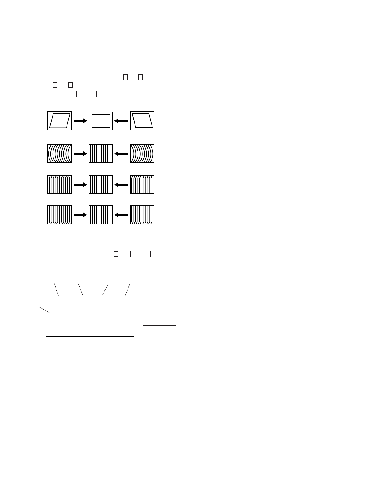
V. ANGLE (VANG), V. BOW (VBOW),
UPPER PIN (UPIN) AND LOW PIN (LPIN)
ADJUSTMENTS
1. Input a crosshatch signal.
2. Activate the Service Adjustment Mode.
3. Select VANG, VBOW, UPIN, and LPIN with 1 and 4.
4. Adjust with
5. Press
3
and 6 for the best picture.
ENTER
MUTING
then
V ANGLE (VANG)
V BOW (VBOW)
UPPER PIN (UPIN)
to save into the memory.
KV-27FS100L/29FS100L
LOW PIN (LPIN)
SERVICE ADJUSTMENT MODE MEMORY
ENTER
0
Item
then
7
.
Item
Data
Green
0
Red
ENTER
1. After completing all adjustments, press
Read From Memory
Display
Mode
Category
service defl vbow
Signal
Type
ntsc
vchp
00000000 00000000
— 28 —
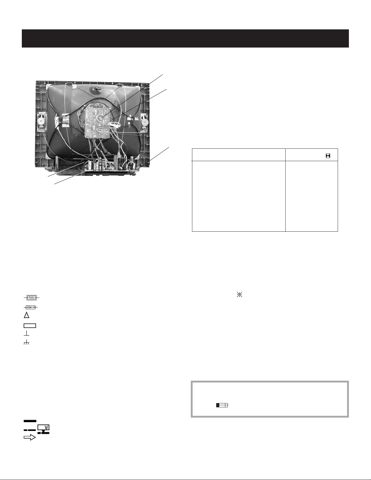
SECTION 5: DIAGRAMS
KV-27FS100L/29FS100L
5-1. CIRCUIT BOARDS LOCATION
HS Board
A Board
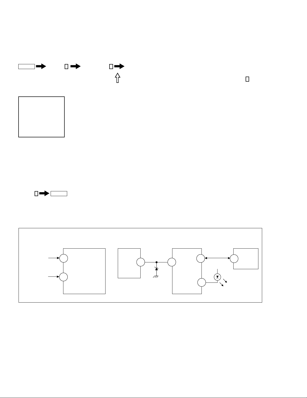
5-2. PRINTED WIRING BOARD AND SCHEMATIC DIAGRAM INFORMATION
CV Board
V Board
D Board
The components identifi ed by X in this basic schematic diagram have
been carefully factory-selected for each set in order to satisfy regulations
regarding X-ray radiation. Should replacement be necessary, replace
only with the value originally used.
When replacing components identifi ed by
Y
, make the necessary
adjustments as indicated. If the results do not meet the specifi ed value,
change the component identifi ed by
X
and repeat the adjustment until
the specifi ed value is achieved. (Refer to Section 3: Safety Related
Adjustments on Page 15.)
When replacing the parts listed in the table below, it is important to
perform the related adjustments.
Part Replaced ( )
Y
DY, T585, CRT, IC001, IC561,
IC600, IC604, C506,C507,C508,
Adjustment ( )
HV HOLD-DOWN
R564
C510, C511, C513, C514, L588,
D565, D566, D567,PH602,R564,
R585, R588,R628, R851,T510,
T511....................A Board
All capacitors are in µF unless otherwise noted. pF : µµF 50WV or less
are not indicated except for electrolytics and tantalums.
All electrolytics are in 50V unless otherwise specifi ed.
All resistors are in ohms. k=1000, M=1000k
Indication of resistance, which does not have one for rating electrical
power, is as follows: Pitch : 5mm Rating electrical power :
1
/
W in resistance, 1/
4
W and 1/
10
W in chip resistance.
8
: nonfl ammable resistor.
: fusible resistor.
: internal component.
: panel designation and adjustment for repair.
: earth ground
: earth-chassis
All variable and adjustable resistors have characteristic curve B, unless
otherwise noted.
Readings are taken with a color-bar signal input.
REFERENCE INFORMATION
RESISTOR : RN METAL FILM
: RC SOLID
: FPRD NONFLAMMABLE CARBON
: FUSE NONFLAMMABLE FUSIBLE
: RW NONFLAMMABLE WIREWOUND
: RS NONFLAMMABLE METAL OXIDE
: RB NONFLAMMABLE CEMENT
: ADJUSTMENT RESISTOR
COIL : LF-8L MICRO INDUCTOR
CAPACITOR : TA TANTALUM
: PS STYROL
: PP POLYPROPYLENE
: PT MYLAR
: MPS METALIZED POLYESTER
: MPP METALIZED POLYPROPYLENE
: ALB BIPOLAR
: ALT HIGH TEMPERATURE
: ALR HIGH RIPPLE
Readings are taken with a 10M digital multimeter.
Voltages are DC with respect to ground unless otherwise noted.
Voltage variations may be noted due to normal production tolerances.
All voltages are in V.
S : Measurement impossibillity.
: B+line.
: B-line. (Actual measured value may be different).
: signal path. (RF)
Circled numbers are waveform references.
The components identifi ed by shading and ! symbol are critical for safety. Replace
only with part number specifi ed.
The symbol indicates a fast operating fuse and is displayed on the component
side of the board. Replace only with fuse of the same rating as marked.
— 29 —
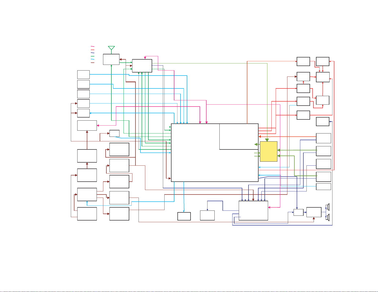
5.3. BLOCK DIAGRAM AND SCHEMATICS
Communication
IIC
Picture Signal
Picture Signal
Sound Signal
Sound Signal
Tuning Related
Tuning Related
Control Lines
Control Lines
Power
Power
Power
Power
Front
Front
Panel
Panel
Keys
Keys
Menu
Menu
Keys
Keys
Receiver
Receiver
Stand by/
Stand by/
Timer
Timer
($A0,$A2,$A4,
($A0,$A2,$A4,
$A6,$A8,$AA)
$A6,$A8,$AA)
5V Stand-by
5V Stand-by
Energy Star
Energy Star
Main Power
Main Power
Key
Key
IR
IR
Led
Led
M24C16
M24C16
Supply
Supply
AC Line
AC Line
Antena
Antenna
Switch
Switch
Reset
Reset
5V Regulator
5V Regulator
9V Regulator
9V Regulator
Low B
Low B
Rectifier
Rectifier
12.5V
12.5V
Audio
Audio
Rectifier 14V
Rectifier 14V
B+ Rectifier
B+ Rectifier
115V
115V
Main Tuner
Main Tuner
($C0)
($C0)
I-MENU
I-MENU
I-KEY
I-RMCN
I-KEY
I-RMCN
O-LED
O-LED
I-AFT2
I-AFT2
I-AFT
I-AFT
O-AGCMUTE
O-AGCMUTE
O-ANTSW
O-ANTSW
I-SAP
I-SAP
I-STEREN
I-STEREN
O-MONO
O-MONO
O-SAP
O-SAP
I-RESET
I-RESET
VCC O-MUTE
VCC O-MUTE
O-DGC
O-DGC
O-RELAYN
O-RELAYN
Degauss
Degauss
SW
SW
IO-BDAT
IO-BDAT
IO-SDAT
I-POWERN
I-POWERN
IO-SDAT
O-BCLKN
O-SCLKN
O-BCLKN
O-SCLKN
Micro
Micro
M65582MF-XXXFP
M65582MF-XXXFP
($60)
Audio
Audio
Out
Out
Video Processor/Comb Filter
Video Processor/Comb Filter
($??)
O-SEL0
O-SEL0
O-SEL1
O-SEL1
I-MECSVD
I-MECSVD
Audio Inputs
Audio Inputs
Audio Processor
Audio Processor
NJM1134
NJM1134
Audio Outputs
Audio Outputs
I-HLDWN
I-HLDWN
O-NS
O-NS
($82)
($82)
Video SW
Video SW
Mute
Mute
FBT
FBT
H-Out
H-Out
V-Out
V-Out
RGB
RGB
Amp
Amp
VM
VM
Audio Amp.
Audio Amp.
TDA8580Q
TDA8580Q
KV-27FS100L/29FS100L
Tilt
Tilt
Rotation
Rotation
CRT
CRT
DY
DY
Monitor
Monitor
Out
Out
Video 4
Video 4
Video 3
Video 3
Video 2
Video 2
Video 1
Video 1
Mechanical
Mechanical
S-Video
S-Video
— 30 —
 Loading...