

Page 1
SELF-DIAGNOSTIC FUNCTION
®
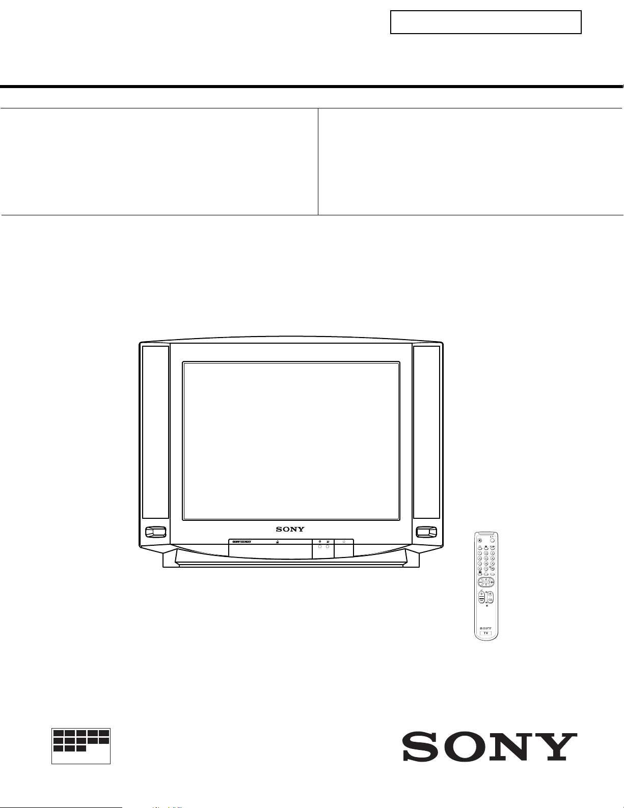
SERVICE MANUAL FE-1
MODEL
KV-21M5D
KV-21T5D
KV-21M5K
COMMANDER DEST CHASSIS NO.
RM-883 AEP SCC-Q04M-A
RM-883 AEP SCC-Q04N-A
RM-883 OIRT SCC-Q03V-A
MODEL
KV-21T5K
KV-21T5R
COMMANDER DEST CHASSIS NO.
RM-883 OIRT SCC-Q03X-A
RM-883 OIRT SCC-Q03W-A
CHASSIS
MICROFILM
N/
MENU
PROGR
Layer 1
RM-883
TRINITRON
1
COLOR TV
®
Page 2
ITEM MODEL Television System Channel Coverage Color System
AEP
OIRT
MODEL 21M5D
Power Consumption
B/G/H
B/G/H, D/K
21T5D
60W 60W 60W
21M5K
21T5K
VHF : E2-E12, A-H2, R01-R12
UHF : E21-E69, B21-B69, R21-R69
CABLE TV : S01-S05, S1-S20
HYPER : S21-S41
VHF : E2-E12, R01-R12
UHF : E21-E69, R21-R60
CABLE TV : S01-S03, S1-S20
HYPER : S21-S41
21T5R
PAL, SECAM
PAL, SECAM
NTS04.43, NTSC3.58
(VIDEO IN)
[PICTURE TUBE]
Super Trinitron
Approx. 55cm (21 inches)
(Approx. 51cm picture measured
diagonally)
110 degree deflection
Input/Output Terminals
[REAR]
21-pin Euro connector (CENELEC standard).
- Inputs for Audio and Video signals.
- Inputs for RGB.
- Outputs of TV Video and Audio signals.
[FRONT]
Video input - phono jack
Audio inputs - phono jacks
Headphone jacks : minijack
Sound output 2 x 4.5W (Music Power)
Power requirements 220 - 240V
Dimensions Approx 598x456x467mm
Weight Approx 21kg
Supplied accessories RM-883 Remote Commander (1)
IEC designated R6 battery (2)
Other features TELETEXT (For KV-21T5 models)
[RM-883]
Remote control system Infrared control
Power requirements 1.5V dc
2 batteries IEC designation
R6 (size AA)
Dimensions Approx 65x225x21mm (w/h/d)
Weight Approx 157g (Not including battery)
Design and specifications are subject to change without notice.
2
Page 3
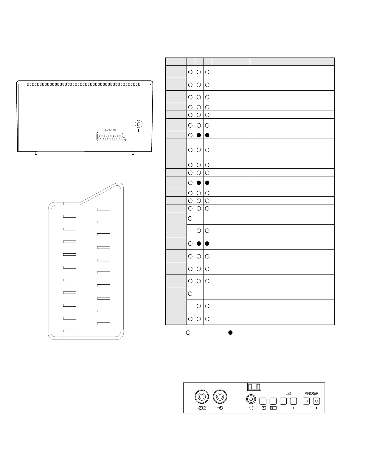
Model Name
KV-21M5D
KV -21M5K
Item
Pal Comb
PIP
Woofer Box
Scart 1
Scart 2
Front in (3)
Scart 4
Projector
AKB in 16:9 mode
Norm B/G
Norm I
Norm D/K
Norm AUS
Norm L
Norm SAT
Norm M
KV -21T5D
OFF OFF OFF
OFF OFF OFF
OFF OFF OFF
ON ON ON
OFF OFF OFF
ON ON ON
OFF OFF OFF
OFF OFF OFF
ON ON ON
ON ON ON
OFF OFF OFF
OFF ON ON
OFF OFF OFF
OFF ON OFF
OFF OFF OFF
OFF OFF OFF
KV -21T5K
KV -21T5R
Language Preset
German OIRT OIRT
3
Page 4
21
19
17
15
13
11
9
7
5
3
1
20
18
16
14
12
10
4
2
Pin No 1 2 4 Signal Signal level
1
2
3
4
5
6
7
8
9
10
11
12
13
14
15
_ (S signal Chroma
16
17
18
8
19
6
20
_ Video input
21
Audio output B
(right)
Audio output B
(right)
Audio output A
(left)
Ground (audio)
Ground (blue)
Audio input A
(left)
Blue input 0.7 +/- 3dB, 75 ohms positive
Function select
(AV control)
Ground (green)
Open
Green Green signal : 0.7 +/- 3dB, 75 ohms,
Open
Ground (red)
Ground (blanking)
_ _ Red input 0.7 +/- 3dB, 75 ohms, positive
input)
Blanking input
(Ys signal)
Ground (video
output)
Ground (video
input)
Video output 1V +/- 3dB, 75ohms, positive sync 0.3V
_ _ Video input 1V +/- 3dB, 75ohms, positive sync 0.3V
Y (S signal)
Common ground
(plug, shield)
Standard leve l : 0.5V rms
Output impedence : Less than 1kohm*
Standard leve l : 0.5V rms
Output impedence : More than 10kohm*
Standard leve l : 0.5V rms
Output impedence : Less than 1kohm*
Standard leve l : 0.5V rms
Output impedence : More than 10kohm*
High state (9.5-12V) : Part mode
Low state (0-2V) : TV mode
Input impedence : More than 10K ohm s
Input capacitance : Less than 2nF
positive
0.3 +/- 3dB, 75 ohms, positive
High state (1-3V) Low state (0-0.4V)
Input impedence : 75 ohms
(-3+10dB)
(-3+10dB)
1V +/- 3dB, 75ohms, positi ve sync 0.3V
(-3+10dB)
4
Page 5

TABLE OF CONTENTS
Section Title Page Section Title Page
1. GENERAL
5. DIAGRAMS
Overview of TV b u tto ns .....................6
Using Select Mode ................... ..6
Adjusting the Picture .....................7
Using the Sleep Timer .....................7
Using the Wake Up Timer .....................8
Viewing Telete xt ................... ..8
Exchanging Programme Pos .....................9
Manually Tuning the TV .....................9
Fine-Tuning Channels .....................10
Skipping Programme Pos .....................10
Using Optional Equipment ................... ..1 1
Troubles h oo tin g ................... ..1 1
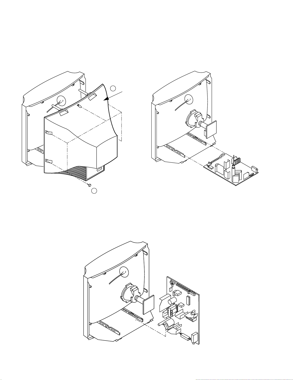
2. DISASSEMBLY
2-1. Rear Cover Removal .....................12
2-2. Chassis Assy Removal .....................1 2
2-3. Service Position .....................12
2-4. Picture Tube Removal .....................13
3. SET-UP ADJUSTMENTS
3-1. Beam Landing .....................14
3-2. Convergence .....................15
3-3. Screen [G2] White Balance .....................17
3-4. Focus .....................17
5-1. Block Diagrams .....................23
5-2. Circuit Board Location .....................27
5-3. Schematic Diagrams and
Printed Wiring Boards .....................27
* A Board .....................31
* C Board .....................36
5-4. Semiconductors .....................39
5-5. IC Blocks .....................40
6. EXPLODED VIEWS
6-1. Chassis .................... .41
6-2. Picture Tube .....................42
7. ELECTRICAL PARTS LIST
.....................43
4. CIRCUIT ADJUSTMENTS
4-1. Electri cal Adju stm en ts .....................18
4-2. Test Mode 2 .....................21
4-3. FE-1 Self Diagnostic Software .....................22
CAUTION
SHORT CIRCUIT THE ANODE OF THE PICTURE TUBE AND THE
ANODE CAP TO THE METAL CHASSIS, CRT SHIELD, OR THE
CARBON PAINTED ON THE CRT, AFTER REMOVAL OF THE
ANODE CAP
WARNING !!
AN ISOLATING TRANSFORMER SHOULD BE USED DURING ANY
SERVICE WORK TO AVOID POSSIBLE SHOCK HAZARD DUE TO
LIVE CHASSIS. THE CHASSIS OF THIS RECEIVER IS DIRECTLY
CONNECTED TO THE POWER LINE.
SAFETY-RELATED COMPONENT WARNING !!
COMPONENTS IDENTIFIED BY SHADING AND MARKED ON
THE SCHEMATIC DIAGRAMS, EXPLODED VIEWS AND IN THE
PARTS LIST ARE CRITICAL FOR SAFE OPERATION. REPLACE
THESE COMPONENTS WITH SONY PARTS WHOSE PART NUMBERS
APPEAR AS SHOWN IN THIS MANUAL OR IN SUPPLEMENTS
PUBLISHED BY SONY.
ATTENTION
APRES AVOIR DECONNECTE LE CAP DE’LANODE,
COURT-CIRCUITER L’ANODE DU TUBE CATHODIQUE ET
CELUI DE L’ANODE DU CAP AU CHASSIS METALLIQUE
DE L’APPAREIL, OU AU COUCHE DE CARBONE PEINTE
SUR LE TUBE CATHODIQUE OU AU BLINDAGE DU TUBE
CATHODIQUE.
ATTENTION !!
AFIN D’EVITER TOUT RISQUE D’ELECTROCUTION PROVENANT
D’UN CHÁSSIS SOUS TENTION, UN TRANSFORMATEUR
D’ISOLEMENT DOIT ETRE UTILISÈ LORS DE TOUT DÈPANNAGE.
LE CHÁSSIS DE CE RÈCEPTEUR EST DIRECTMENT RACCORDÈ
Á L’ALIMENTATION SECTEUR.
ATTENTION AUX COMPOSANTS RELATIFS Á LA
SÈCURITÈ !!
LES COMPOSANTS IDENTIFIÈS PAR UNE TRAME ET PAR UNE
MARQUE SUR LES SCHÈMAS DE PRINCIPE, LES VUES
EXPLOSÈES ET LES LISTES DE PIECES SONT D’UNE IMPORTANCE
CRITIQUE POUR LA SÈCURITÈ DU FONCTIONNEMENT, NE LES
REMPLACER QUE PAR DES COMPSANTS SONY DONT LE NUMÈRO
DE PIÈCE EST INDIQUÈ DANS LE PRÈSENT MANUEL OU DANS
DES SUPPLÈMENTS PUBLIÈS PAR SONY.
5
Page 6

7
RM-883
PROGR
MENU
/
Basic TV Features
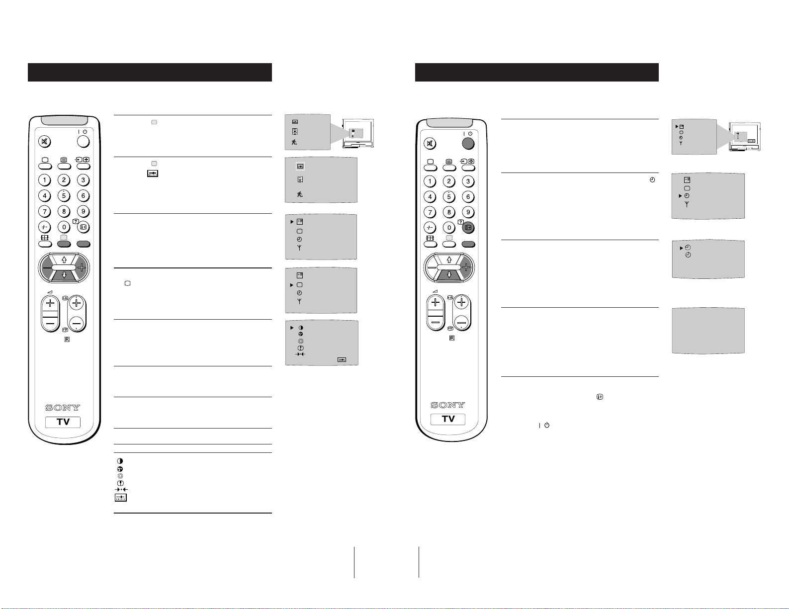
Overview of TV Buttons
On/Off Switch.
Programme Up or
Down Buttons.
(selects TV channels).
Volume Control Buttons.
Auto Tune
Button.
Video Input Button.
(selects input signals
from VCR etc.).
Overview of Remote Control Buttons
To Mute Sound
Press to mute TV sound. Press again
to restore the sound.
To Change Screen Format
Press to view programmes in 16:9
mode.
Press again to return to 4:3 mode.
To Adjust TV Volume
Press to adjust the volume of the TV.
To Temporarily Switch Off TV
Press to temporarily switch off TV. Press
again to switch on TV from standby
mode.
To save energy we recommend switching off
completely when TV is not in use.
NOTE: After 15 - 30 minutes without a
TV signal and without any button being
pressed, the TV switches automatically
into standby mode.
To Reveal On Screen Information
Press to reveal all on-screen indications.
Press again to cancel.
To Select Channels
Press to select channels.
To Select Channels
Press to select channels.
For double-digit programme
numbers, e.g. 23, press -/-- first,
then the buttons 2 and 3.
If you enter an incorrect first
digit, this should be corrected by
entering another digit (0 - 9) and
then selecting -/-- button again to
enter the programme number of
your choice
SECTION 1 GENERAL
Additional TV Features
Using Select Mode
You can select different preset picture modes.
The operating instructions mentioned here are partial abstracts
from the Operating Manual. The page numbers of the Operating
Instruction Manual remain as in the manual.
6
SELEC
1 Press the MENU button on the remote control to
/
display the menu on the TV screen.
2 With the cursor pointing at the
TV screen as shown, press the yellow button.
symbol on the
SELEC
T
T
SELEC
T
SELEC
T
OK
3 Press the blue button to select the desired mode:
MENU
PROGR
RM-883
Personal Mode - reverts to settings made in
“Adjusting the Picture” section of the manual.
Movie Mode - for films
Live Mode - for live broadcast programmes
4 Press the MENU button to remove the menu
display from the TV screen.
Note: The mode selected in step 3 is now stored.
Changing Modes Quickly
1
Press the button on the remote control to display
the three different modes.
2 Press the button again to select your desired
mode.
8
Page 7
Additional TV Features
Adjusting the Picture
Additional TV Features
Using the Sleep Timer
Although the picture is adjusted at the factory, you can modify it to suit your own
requirement.
1 Press the button on the remote control to
/
display the three different modes on the TV
screen.
2 Press the button to highlight the personal mode
as shown.
MENU
symbol
3 Press the MENU button to display the menu on
the TV screen.
4 Press the blue button on the control to select the
symbol on the TV screen then press the yellow
PROGR
button.
7
5 Press the blue button to select the item you wish
RM-883
to change (see below).
6 Press the red or yellow button to alter the selected
item.
7 Press the MENU
display from the TV screen.
button to remove the menu
SELEC
T
SELEC
T
IIIIIIIIIIIIIII- - - - - IIIIIIIIIIIIIII- - - - - -
IIIIIIIIIIIIIII- - - - - IIIIIIIIIIIIIII- - - - - -
The TV may be set to switch automatically to the standby mode after a length of time
chosen by you. You may set the time in 15 minute steps up to 4 hours.
1 Press the MENU button on the remote control to
/
display the menu on the TV screen.
2 Press the blue button on the control to select the
symbol on the TV screen, then press the yellow
button.
MENU
3 Press the yellow button repeatedly until the
required amount of time delay appears on the
screen.
PROGR
4 Once the time delay has been selected, press the
MENU button to remove the on-screen display.
RM-883
One minute before standby, the display shown
appears on the screen.
Notes:
• When watching TV, press the
time remaining.
• To return to normal operation from standby mode,
press the
button.
button to display
SELEC
T
0:59
SELEC
T
OK
SELEC
T
0:45
OFF
Symbol Item
• Contrast
• Colour
• Brightness
• Sharpness
• Reset - resets to factory preset picture level
• Represents the mode selected in the “Using
Select Mode” section.
9
10
Page 8
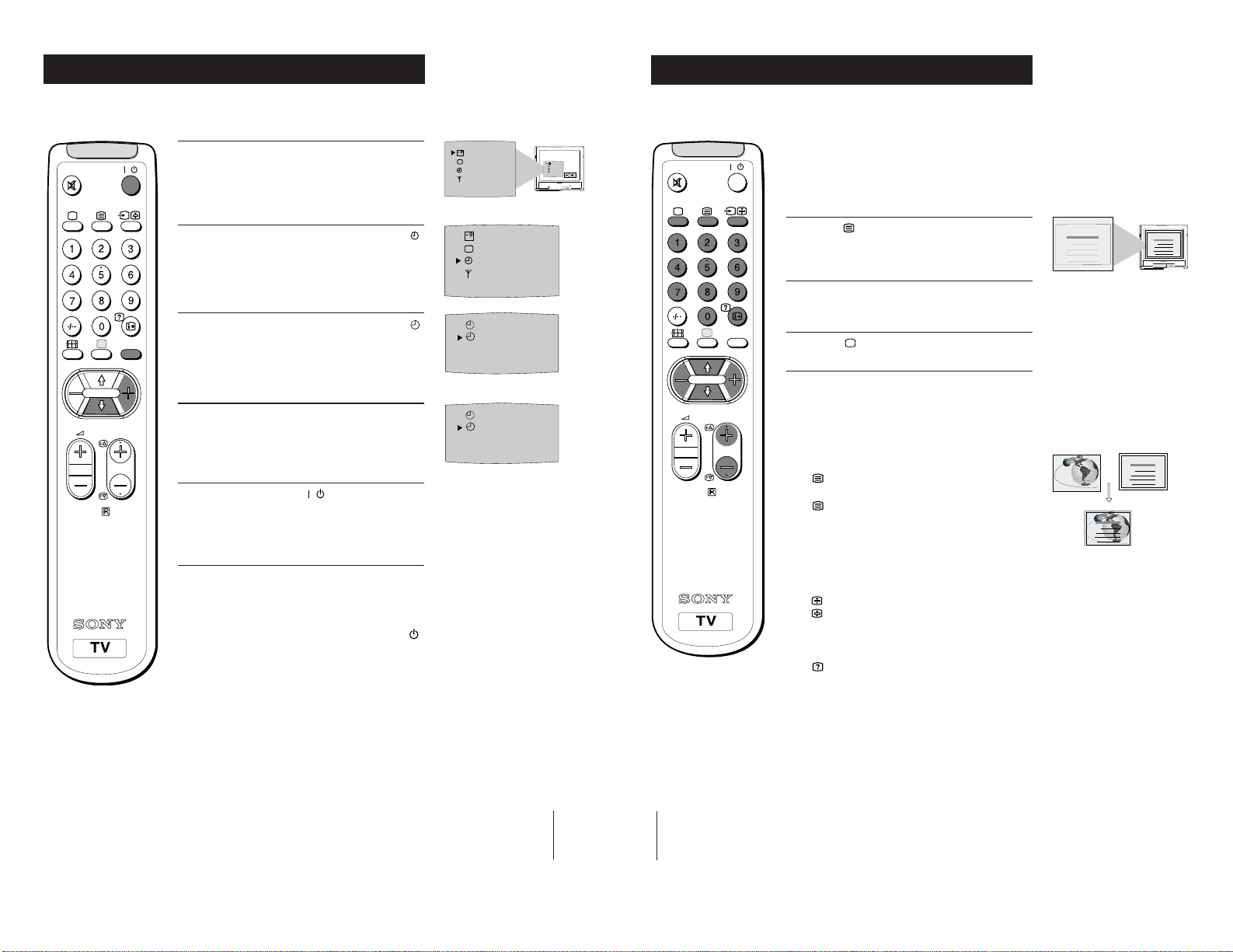
Additional TV Features
Using the Wake Up Timer
Additional TV Features
Viewing Teletext (KV-21T5D only)
The TV may be set to switch on automatically after a length of time chosen by you.
You may set the time in 15 minute steps up to 12 hours.
1 Press the MENU button on the remote control to
/
display the menu on the TV screen.
2 Press the blue button on the control to select the
symbol on the TV screen, then press the yellow
button.
3 Press the blue button on the control to select the
MENU
symbol on the TV screen, then press the yellow
button.
4 Press the red or yellow button to set the time.
PROGR
8
RM-883
0:00 (OFF) 0:15 0:30 0:45 -----12:00
5 Press the standby button
The standby indicator on the TV flashes regularly
to indicate that the Wake Up Timer is active.
After the selected length of time, the TV switches
on automatically.
.
Notes:
• If you use the “Wake Up Timer” to switch the TV
on and for one hour after switching on, no TV or
Remote Control button is pressed, the TV switches
itself back into Standby mode and the indicator
on the TV lights.
• Any temporary power failure will cause a
misfunction in the “Wake Up Timer” and you will
have to reset the “Wake Up Timer”.
Teletext is an information service transmitted by most TV stations.
SELEC
T
SELEC
T
OFF
OFF
OFF
0:45
SELEC
T
OK
/
MENU
PROGR
RM-883
Selecting Teletext
Press a number button on the remote control to
1
select the channel which carries the teletext service
you wish to receive.
2 Press the button on the remote control to switch
on teletext.
3 Input three digits for the page number using the
numbered buttons on the control.
4 Press the button to switch off teletext.
Note: Teletext errors may occur if the broadcasting
signals are weak.
Using Other Teletext Functions
To Superimpose Teletext on to the TV
once in teletext mode or twice in TV mode to
Press
superimpose teletext on to the TV screen.
again to cancel teletext mode.
Press
To Move to Next or Preceding Page
Press PROGR +/previous or next page.
on the remote control to select the
TELETEXT
Index
Programme
News
Sport
Weather
25
153
101
98
TELETEXT
Index
Programme
News
Sport
Weather
TELETEXT
Index
Programme
News
Sport
Weather
25
153
101
98
TELETEXT
Index
Programme
News
Sport
Weather
25
153
101
98
25
153
101
98
To Freeze a Teletext Page
on the control to freeze the page.
Press
Press
again to cancel the freeze.
Revealing concealed information (eg: answers
to a quiz).
to reveal information.
Press
Press again to conceal the information.
Using colour buttons to access pages (Fastext)
When the colour coded menu appears at the bottom of
a page, press the colour button (green, red, yellow or
blue) to access the corresponding page.
11
12
Page 9

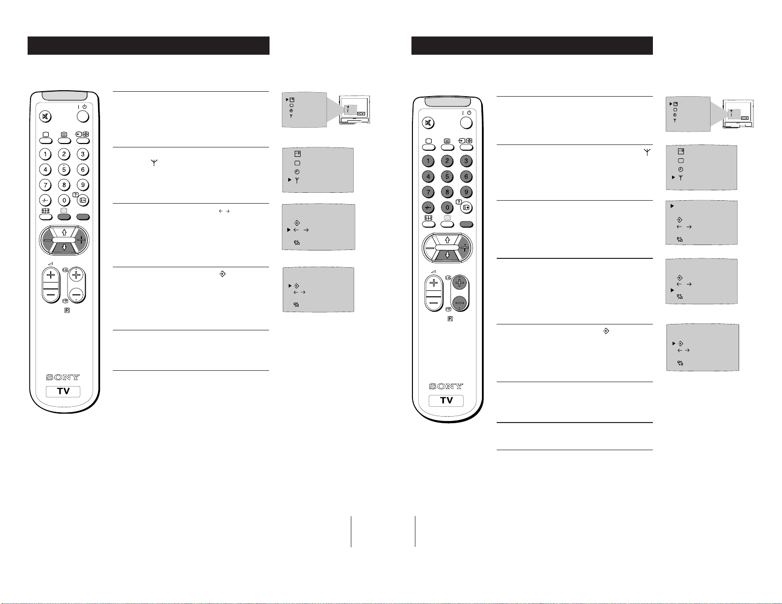
Additional TV Features
Additional TV Features
Exchanging Programme Positions
After tuning you may wish to change the order in which the channels appear on the
TV. You may wish for example to exchange the channel on programme number 8
with the channel on programme number 4.
1 Press the MENU button on the remote control.
/
2 Press the blue button on the control to select on
the TV screen, then press the yellow button.
3 Press the blue
MENU
PROGR
9
RM-883
yellow button.
4 With the cursor pointing at PROGR on the TV
screen as shown, press PROGR + or - button until
the channel you wish to rearrange appears on
screen, then press the blue button once.
5 Press the red or yellow
programme number (e.g. PROGR 04) for your
selected channel.
button to select then press the
button to select the new
SELEC
T
SELEC
T
PROGR 01
VL IIIIIIIIIIIIIII- - - - - - - -
F
C
OO
PROGR - +
01
PROGR - +
04
Manually Tuning the TV
You have already tuned the TV to receive all available channels using the
`Automatically Tuning the TV' procedure at the start of this manual. You can
however carry out this operation manually using the following instructions.
SELEC
SELEC
T
OK
/
MENU
1 Press the MENU button on the remote control to
display the menu on the TV screen.
2 Press the blue button to select the symbol on the
TV screen then press the yellow button.
3 With the cursor pointing at PROGR on the TV
screen as shown, press PROGR + or - button on the
remote control to allocate a programme number to
the channel (eg PROGR 01). For double digit
numbers e.g. 55, press the -/-- button on the remote
control then the corresponding numbered buttons.
4 Press the blue button to select the tuning bar scale
PROGR
RM-883
then press the yellow or red button once to start the
channel search. (Yellow to search up the scale or
red to search down). When a channel is found it
appears on the TV screen.
5 If you do not wish to store this channel on the
programme number you selected, press the yellow
or red button to continue searching for the desired
channel.
T
SELEC
T
PROGR 01
VL IIIIIIIIIIIIIII- - - - -
F
C
OO
PROGR 01
VL IIIIIIIIIIIIIII- - - - -
F
C
OO
SELEC
T
OK
6 Press the blue
yellow button to exchange the channels.
button to select then press the
7 Repeat steps 4 to 6 if you wish to change the order
of the other channels on your TV, then press
MENU to return to normal TV screen.
8 Press the PROGR+/- button to view your selected
channels on their new programme numbers.
PROGR - +
04
13
14
6 If this is the channel you wish to store, press the
blue button to select the
then press the yellow button to store.
7 Repeat steps 3 to 6 if you wish to store more
channels then press the MENU
the menu from the TV screen.
symbol on the screen
button to remove
PROGR 01
VL IIIIIIIIIIIIIII- - - - - - - -
F
COO
Page 10
Additional TV Features
Additional TV Features
Fine-Tuning Channels
If a channel is slightly off tune, you can use this fine tune procedure to obtain a better
picture reception.
1 With the channel you wish to fine-tune on the
/
MENU
PROGR
10
RM-883
screen, press the MENU button on the remote
control. The menu display appears on the TV
screen.
2 Press the blue button on the remote control to
select the
the yellow button.
symbol on the TV screen then press
3 Press the blue button to select the
the TV screen then press the red or yellow button
to adjust the tuning.
4 Press the blue button to select the symbol on the
TV screen then press the yellow button to store.
5 Press the MENU button to remove the menu from
the TV screen.
symbol on
F
SELEC
T
SELEC
T
PROGR 01
VL IIIIIIIIIIIIIII- - - - -
F
C
OO
PROGR 01
VL IIIIIIIIIIIIIII- - - - - - - -
F
C
OO
Skipping Programme Positions
You can programme this TV to skip any unwanted programme numbers when they
are selected with the PROGR +/- buttons.
SELEC
T
OK
/
1 Press the MENU button on the remote control to
display the menu on the TV screen.
2 Press the blue button on the control to select the
symbol on the TV screen then press the yellow
button.
3 With the cursor pointing at PROGR on the TV
MENU
PROGR
RM-883
screen as shown, press PROGR + or - button on the
remote control to select the programme number
you want to skip.
4 Press the blue button to select Coo on the TV menu
screen then press the yellow button on the remote
control.
5 Press the blue button to select the symbol on the
TV screen then press the yellow button to store.
SELEC
T
SELEC
T
PROGR 01
VL IIIIIIIIIIIIIII- - - - -
F
C
OO
PROGR 01
VL IIIIIIIIIIIIIII- - - - -
F
C
OO
PROGR 01
VL IIIIIIIIIIIIIII - - - - - - - -
F
C
OO
SELEC
T
OK
15
16
6 Repeat steps 3 to 5 to skip other unused
programme positions.
7 Press the MENU
the TV screen.
Note: If you wish, you can still select any skipped
programme number by pressing the corresponding
numbered buttons on the remote control.
button to remove the menu from
Page 11
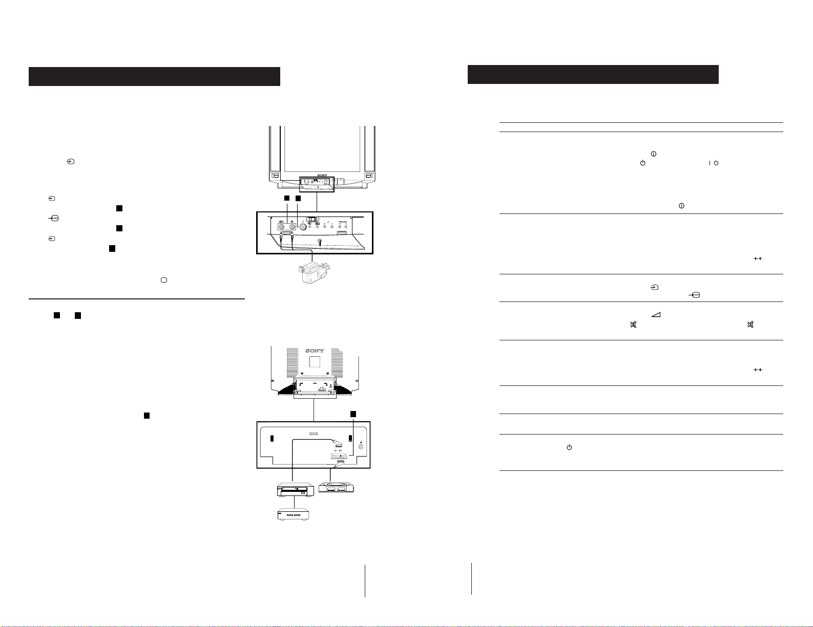
Optional Connections
Using Optional Equipment
Additional Information
Troubleshooting
You can connect optional audio or video equipment to your TV, such as a VCR, a
camcorder or video games as shown.
Select and View the Input Signal
Connect your equipment to the designated TV socket.
1
2 Press
correct input symbol appears on the TV screen.
Symbol Input signals
button repeatedly on your remote control until the
the
• Audio/video input signal through the Euro AV
1
2
connector
• RGB input signal through the Euro AV
connector
• Audio/video input signal through the phono
sockets
C
C
A
3 Switch on the connected equipment.
4 To return to normal TV picture, press the
control.
Note: To avoid picture distortion, do not connect equipment to the
11
and C
A
connectors
at the same time.
button on the remote
Additional Information
Connecting a VCR
We recommend you tune in the VCR signal to TV programme number `0'
using the `Manually Tuning in the TV' section of this instruction manual.
Connecting Headphones
Plug in your headphones to the socket
B
on the front of the TV set.
A
Front of TV
B
Rear of TV
8mm/Hi8
camcorder
C
Here are some simple solutions to problems which may affect the picture and sound.
Problem Solution
No picture (screen is dark), no sound • Plug the TV in.
Poor or no picture (screen is dark), • Using the MENU system, select the Picture
but good sound Adjustment display.
Poor picture quality when watching • Press the button repeatedly on the remote control
a RGB video source. until the RGB symbol
Good picture, no sound • Press the +/– button on the remote control.
No colour on colour programmes • Using the MENU system, select the Picture
Distorted picture when changing • Turn off any equipment connected to the 21 pin
programmes or selecting teletext Euro connector on the rear of the TV.
Remote control does not function • Replace the batteries
• Press the
• If the
programme number button on the remote control.
• Check the aerial connection.
• Check that the selected video source is on.
• Turn the TV off for 3 or 4 seconds and then turn it
on again using the
Adjust the brightness, picture and colour balance
levels.
• From the Picture Adjustment display select
return to the factory settings.
• If
on the remote control.
Adjustment display. Adjust the colour balance.
• From the Picture Adjustment display select
return to the factory settings.
button on the front of TV.
indicator is on press
button on the front of the TV.
is displayed on the screen, press the button
button or a
to
is displayed on the screen.
to
VCR
Decoder
1/
2
1
“PlayStation”
17
18
The standby indicator on the • Contact your nearest Sony service centre.
TV flashes even though the
“Wake Up Timer”is not in use.
• If you continue to have these problems, have your TV serviced by qualified
personnel.
• NEVER open the casing yourself.
Page 12
SECTION 2
DISASSEMBLY
2-1. REAR COVER REMOVAL
2-2. CHASSIS ASSY REMOVAL
2 Rear Cover
1 5 Screws BTV 4x16
2-3. SERVICE POSITION
12
Page 13

2-4. PICTURE TUBE REMOVAL
Degaussing coils 6
Spring tension 7
C board 3
Four PT screws 8
5 DGC holder
2 A Board
Anode cap 1
4 Deflection yoke
Picture tube 9
Cushion
• REMOVAL OF ANODE-CAP
Note : Short circuit the anode of the picture tube and the anode cap to the metal chassis, CRT shield or carbon paint on the CRT, after removing the anode.
* REMOVING PROCEDURES.
c
a
1
Turn up one side of the rubber cap in
the direction indicated by the arrow a
• HOW TO HANDLE THE ANODE-CAP
b
b
2 Using a thumb pull up the rubber cap
firmly in the direction indicated by the
arrow b
3 When one side of the rubber cap is
Anode button
separated from the anode button, the
anode-cap can be removed by turning
up the rubber cap and pulling it up in
the direction of the arrow c
1 To prevent damaging the surface of the anode-cap do not use sharp materials.
2 Do not apply too great a pressure on the rubber, as this may cause damage to the
anode connector.
3 A metal fitting called a shatter hook terminal is fitted inside the rubber cap.
Do not turn the rubber foot over excessively this may cause damage if the shatter
hook sticks out.
13
Page 14

SECTION 3
GREEN
BLUE
RED
SET-UP ADJUSTMENTS
• When complete readjustment is necessary or a new
picture tube is installed, carry out the following
adjustments.
• Unless there are specific instructions to the contrary,
carry out these adjustments with the rated power supply.
• Unless there are specific instructions to the contrary, set the
controls and switches to the following settings :
Contrast ............... 80% [or remote control normal]
Brightness ............... 50%
Preparation:
1. In order to reduce the influence of geomagnetism on the set’s
picture tube, face it in an easterly or westerly direction.
2. Switch on the TV set’s power and degauss with the
degausser.
3-1. BEAM LANDING
1. Input an all-white signal from the pattern generator.
Set the Contrast and Brightness to normal.
2. Set the pattern generator raster signal to all Red.
3. Move the deflection yolk forward and adjust with the purity
control so that the Red is at the centre and the Blue and Green
take up equally sized areas on each side of the screen.
[See Fig.3-1 - 3-3].
4. Move the deflection yolk forward and adjust so that the entire
screen becomes Red. [See Fig.3-1].
5. Switch the raster signal to Blue, then to Green and verify the
purity condition.
6. When the position of the deflection yolk has been determined,
fasten the deflection yolk with the screws.
7. If the beam does not land correctly in all the corners, use
magnets to correct it. [See Fig.3-4].
Carry out the following adjustments in this order :
3-1. Beam Landing
3-2. Convergence
3-3. White balance
3-4. Focus
Note : Test equipment required
1. Color bar/pattern generator.
2. Degausser.
3. Oscilloscope.
4. Digital multimeter.
5. DC Power supply.
Fig. 3-2
For 29" models align the neck assy
as indicated below.
Purity Control
A buckle
G1
G2
Deflection Y oke
Fig. 3-3
Purity control corrects
this area.
Disk magnets or
rotatable disk
magnets correct
these areas (a - d).
Neck Assy
Fig. 3-1
14
ab
c
Deflection yolk positioning
corrects these areas.
d
a
c
b
d
Fig. 3-4
Page 15

3-2. CONVERGENCE
Preparation:
• Before starting this adjustment, adjust the focus, horizontal
size and vertical size.
• Minimize the Brightness setting.
• Input a dot pattern from the pattern generator.
(1) Horizontal and vertical static convergence
• Tilt the V.STAT magnet and adjust the static convergence
by opening or closing the V.STAT magnet.
4. If the V .STAT magnet is moved in the direction of the a
and b arrows, the Red, Green and Blue points move as
indicated below.
Centre dot
R
G
H.STAT
B
RV702
R
G
B
V.STAT Magnet
C Board
RV701
SCREEN
1. [Moving horizontally], adjust the H.STAT control so that the
Red, Green and Blue points are on top of each other at the
centre of the screen.
2. [Moving vertically], adjust the V.STAT magnet so that the
Red, Green and Blue points are on top of each other at the
centre of the screen.
3. If the H.STAT variable resistor is unable to bring the Red,
Green and Blue points together at the centre of the screen,
adjust the horizontal convergence wi th the H.STAT variable
resistor and the V.ST AT magnet in the manner indicated below.
[In this case, the H.STAT variable resistor and the V.STAT
magnet influence each other].
15
Page 16

(2) Operation of the BMC (Hexapole) magnet.
RG B R G B R G B
RGBR
B
G
• The respective dot position resulting from moving each
magnet interact, so be sure to perform adjustment whilst
tracking.
Use the H.STAT VR to adjust the Red, Green and Blue dots
so that they coincide at the centre of the screen
[by moving the dots in the horizontal direction].
G
R
B
V.STAT
Purity
BMC (Hexapole)
(3) Dynamic convergence adjustment.
Preparation:
• Before starting this adjustment, adjust the horizontal and
vertical static convergence.
1. Slightly loosen the deflection yolk screws.
R
B
G
B
RG B
G
RG
B
R
G
B
R
B
G
R
2. Remove the deflection yolk spacer.
3. Move the deflection yolk as indicated in the figure below and
optimize the convergence.
4. Tighten the deflection yolk screws.
5. Re-install the deflection yolk spacer.
G
B
B
G
R
R
RG
RG
B
B
R
B
G
RG
B
16
Page 17

(4) Screen corner convergence.
• If you are unable to adjust the corner converge nce pro perly,
this can be corrected by the use of permalloy assemblies.
a
a-d: screen-corner
convergence defect
b
3-3. Screen [G2], White balance
G2 Setting
1. Input a dot signal from the pattern generato r.
2. Set the Picture, Brightness and Colour to minimum .
3. Apply 170Vdc from an external power supply to the
R, G and B cathodes of the CRT.
4. Whilst watching the picture, adjust the G2 control [RV
SCREEN] located on the FBT to the point just before the flyback return lines disappear.
b
Permalloy
d
c
Fit the permalloy assembly to the rear
of the CRT to correct the area at fault.
c
d
a
White balance adjustment
1. Input a ‘PAL’ all-white signal from the pattern generator.
2. Enter into the Service Mode.
3. Enter into the ‘Picture’ service menu.
4. Select the ‘Green drive’ and adjust so that the White Balance
becomes optimum.
5. Select the ‘Blue drive’ and adjust so that the White Balance
becomes optimum.
6. Set the Picture to MIN.
7. Set the ‘R-cut-off’ to 07.
8. Adjust the ‘G-cut-off’, and the ‘B-cut-off’ so that the White
Balance becomes optimum.
10. Press the button to return to TV operation.
PICTURE
R - Drive Adj
G - Drive Adj
B - Drive Adj
R - cut - off Adj
G - cut - off Adj
B - cut - off Adj
ID - start 02
ID - stop 01
ID - level 01
Bellfo Adj
Sub Colour Adj
Sub Brightness Adj
FOCUS
SCREEN
3-4.FOCUS
1. Input a Phillips colour pattern
2. Set the picture settings to normal.
3. Adjust the focus control located on the Flyback transformer to
bring the centre of the screen into focus.
Note :Bring only the centre area of the screen into focus, switch to an
all-white pattern and confirm that the magenta ring is hardly
noticed. To obtain optimum focus balance the focus setting
between optimum screen centre focus and a reduced magenta
ring level.
17
Page 18

CIRCUIT ADJUSTMENTS
4-1.ELECTRICAL ADJUSTMENTS
SECTION 4
Service adjustments to this model can be performed
using the supplied Remote Commander RM-883.
HOW TO ENTER INTO SERVICE MODE
1. Turn on the main power switch and enter into the stand-by
mode.
2. Press the following sequence of buttons on the Remote
Commander.
+
i
(ON SCREEN
DISPLAY)
5
(DIGIT 5)
• ‘TT--’ will appear in the upper right corner of the
screen.
Other status information will also be displayed.
3. Press ‘MENU’ on the remote commander to obtain the
following menu on the screen.
TEST MENU
> Picture
Geometry
Sound
TV Status
AGC Adjust
Technical
4. Move to the corresponding adjustment item using the ‘Green’
[up] or ‘Blue’ [down] buttons on the Remote Commander.
5. Press the ‘Yellow’ button to enter into the required menu item.
6. Press the ‘Menu’ button on the Remote Commander to quit the
Service Mode when all adjustments have been completed.
+
(VOLUME +)
(TV)
PICTURE
R - Drive Adj
G - Drive Adj
B - Drive Adj
R - cut - off Adj
G - cut - off Adj
B - cut - off Adj
ID - start 02
ID - stop 01
ID - level 01
Bell-f0 Adj
Sub Colour Adj
Sub Brightness Adj
GEOMETRY
V centre Adj
V size Adj
V Lin Adj
S Corr Adj
H Cent Adj
H Size Adj
Pin Amp Adj
Corner Pin Adj
Pin Phase Adj
V Bow Adj
V Angle Adj
Upper V Lin Adj
Lower V Lin Adj
Left HBLK 07
Right HBLK 07
CD Mode (AV) 01
SOUND
Nicam Error Lower
Nicam Error Upper
Nicam Error Rate xx
AGC Gain Level xx
20
80
[Status only]
[Status only]
Note :The data shown in the ‘TV STATUS’ table is dependant on
destination and country.
TV STATUS
Destination A/L/E/U/D/B/K/R
Text Language East/West
18
Page 19

TECHNICAL
GD - Secam 30
BD - Secam 31
RC - Secam 11
GC - Secam 19
BC - Secam 10
GD - Sports 30
BD - Sports 36
RC - Sports 14
GC - Sports 15
BC - Sports 17
Y - Delay (AV) 07
Note: Ensure that no signal is applied to the Antenna socket while
carrying out the following IF adjustments.
SYSTEM B/G, D/K, I & L I.F ADJUSTMENT
1. Input a 38.9Mhz carrier signal at 100dBuV to Pin 11 [IF
output] of the tuner [TU101].
2. Measure the voltage at Pin 17 of [IC101].
3. Adjust L103 [A Board] to obtain a voltage of 2.5V +/- 0.3V.
SYSTEM L BAND 1 I.F ADJUSTMENT
1. Input a 34.0MHz carrier signal at 100dBuV to Pin 11 [IF
output] of the tuner [TU101].
2. Select ‘system L’ + C00 [channel 00].
3. Measure the voltage at Pin 17 [IC101].
4. Adjust RV101 [A Board] to obtain a voltage of 2.5V +/- 0.3V.
SUB BRIGHTNESS ADJUSTMENT
1. Input a Phillips colour pattern.
2. Press ‘TEST’ ‘TEST’ 13 on the Remote Commander.
3. Adjust the ‘Sub-Brightness’ data so that there is barely a
difference between the 0 IRE and 10 IRE signal levels.
SUB CONTRAST ADJUSTMENT
1. Input a video signal that contains a small 100% white area on a
black background
2. Set the picture control to maximum. [‘TT01’]
3. Connect an oscilloscope to Pin 1 of CN504 [A Board].
4. Enter into the ‘Picture’ service menu.
5. Adjust the ‘R - Drive’ data to obtain the following waveform.
25" 2.21V +/- 0.01V
29" 2.52V +/- 0.01V
R - out Waveform
SUB COLOUR ADJUSTMENT
1. Receive a PAL colour bar signal.
2. Connect an oscilloscope to Pin 3 of CN504 [A Board].
3. Enter into the ‘Picture’ service menu.
4. Adjust the ‘Sub Colour’ data so that the Cyan, Mag enta and
Blue colour bars are of equal levels as indicated below.
TUNER AGC ADJUSTMENT
1. Receive a signal of 65dBuV / 75 ohm terminated, via the tuner
antenna socket.
2. Connect a voltmeter to JW130 [A Board].
3. Enter into the ‘Test Menu’.
4. Select the ‘AGC Adjust’ menu item.
5. Adjust the data using the Yellow and Green buttons on the
Remote Commander to obtain a voltage of 3.0V +/- 0.2V.
A
RV101
IC101
17
L103
11
JW130
B-Out Wav eform
Same Level
TUNER
A Board component side
19
Page 20

BELL FILTER ADJUSTMENT (
Secam models only
).
Note : Ensure that the TV set has been powered up for at least
1 minute to allow for drift before carrying out the following
adjustment.
1. Input a video SECAM Colour Bar signal via AV1.
2. Connect an oscilloscope to pin 1 of CN504 [R-OUT] on the
A board.
3. Enter into the ‘Picture’ menu and select ‘Bell-f0’.
4. Decrease the register of ‘Bell-f0’ until the following waveform
change between RED and BLUE is obtained.
V SIZE
V LIN
S CORRECTION
V CENTRE
H CENTRE
Before adjustment After adjustment
5. When the correct waveform has been obtained add an
additional 7 steps to the register.
DEFLECTION SYSTEM ADJUSTMENT
1. Enter into the ‘Geometry’ service menu.
2. Select and adjust each item in order to obtain the optimum
image.
GEOMETRY
V centre Adj
V size Adj
V Lin Adj
S Corr Adj
H Cent Adj
H Size Adj
Pin Amp Adj
Corner Pin Adj
Pin Phase Adj
V Bow Adj
V Angle Adj
Upper V Lin Adj
Lower V Lin Adj
Left HBLK 07
Right HBLK 07
CD Mode (AV) 01
H SIZE
PIN AMP
PIN PHASE
CORNER PIN
V ANGLE
20
Page 21

4-2. TEST MODE 2:
Is available by pressing ‘TEST’ button twice, OSD ‘TT’ appears. The functions described below are available by pressing the two numbers. To
release the Test mode 2, press 0 twice, or switch the TV into stand-by mode, or press the TV button on the remote commander.
00 Cancel Test mode
01 Picture maximum
02 Picture minimum
03 Volume 35%
04 Volume 50%
05 Volume 65%
06 Volume 80%
07 Ageing mode On/Off
08 Set shipping conditions
09 Display TV Status
10 No function
11 Sub Picture Adjustment
12 Sub Colour Adjustment
13 Sub Brightness Adjustment
14 Text H position Adjustment
15 Rotation test
16 Picture level 50%
17 Audio mute ON
18 Disable Blanking
19 No function
20 No function
21 Destination A
22 Destination L
23 Destination E
24 Destination U
25 Destination D
26 Destination B
27 Destination K
28 Destination R
29 No function
30 No function
31 Auto shutoff Disable/Enable
32 RGB priority Disable/Enable
33 Rotation On/OFF
34 Text language East/West
35 Wide CRT/4:3 CRT
36 VM ON/OFF test
37 No function
38 No function
39 No function
40 No function
41 Re-initialize the NVM [Only when Prog=59]
42 Re-initialise geometry settings [Only when Prog=59]
43 No function
44 No function
45 No function
46 No function
47 No function
48 Set NVM as NON Virgin [Only when Prog=59]
49 Set NVM as Virgin [Only when Prog=59]
50 No function
51 No function
52 No function
53 No function
54 No function
55 No function
56 No function
57 No function
58 No function
59 No function
60 No function
61 Auto AGC Adjust
62 Alternative Dest B Autotuning
63 Enable/Disable Y/C input
64 Signal Quality Check for Auto Tune
65 Signal Quality NOT Checked for Auto Tune
66 No function
67 Manual AGC Adjust
68 -100 No function
21
Page 22

4-3. FE-1 SELF DIAGNOSTIC SOFTWARE
The identification of errors within the FE-1 chassis is triggered in one of two ways :- 1: Busy or 2: Device failure to respond to IIC. In the event
of one of these situations arising the software will first try to release the bus if busy (Failure to do so will report with continuous flashing LED) and
then communicate with each device in turn to establish if a device is f a ulty. If a device is found to be faulty the relevant device number will be displayed through the LED (Series of flashes which must be counted) See Table 1., non fatal errors are reported using this method.
Each time the software detects an error it is stored within the NVM. See Table 2.
How to enter into Table 2
Table 1
ERROR
No error 00
Not allowed (may be confused with Sircs response
flash!)
Protection circuit trip < ANY TIME > 02
Reserved 03
No vertical sync 04
AKB 05
IIC bus clock and/or data lines low at Power ON 06
NVM no IIC bus acknowledge at Power ON 07
Jungle controller no IIC acknowledge at Power ON 08
Tuner no acknowledge at Power ON 09
Sound processor no acknowledge at Power ON 10
Flash Timing Example : e.g. error number 3
StBy LED
ON ON ON
OFF OFF
LED
ERROR
COUNT
01
1. Turn on the main power switch of the TV set and enter into the
‘Standby Mode’.
2. Press the following sequence of buttons on the Remote
Commander.
+
i
(ON SCREEN
DISPLAY)
5
(DIGIT 5) (VOLUME -)
(TV)
3. The following table will be displayed indicating the error
count.
Tab le 2
Error Times
2 -
3 4 5 6 7 8 9 10 -
Note: To clear the error count data press ‘80’ on the Remote
commander.
22
Page 23

5-1 BLOCK DIAGRAMS
POWER SUPPLY, DEFLECTION,
PROCESSOR, TUNING, VIDEO SIGNAL
PROCESSOR, AV IN/OUT
SWF
101
SDA
SCL
TU101
CN001
SDA
SCL
J402
VIDEO
A ( )
IF1
AGC
SCL
SDA
3
2
4
L
R
1
2
14
+5V
IC101 VIF/SIF
DEMODULATOR
VIF
VIF
STAND SW RF
TU AGC
AF OUT
DET OUT
AGC
AFC
FUNCTION
SWITCH
S001-S006
REMOTE
CONTROL
RECEIVER
IC002
S601
POWER
CN601
CN603
CN602
1
2
1
2
1
3
DGC
CHECK
DGC CHECK
DGC
DGC
D632
RECT
LINE FILTER
T601
RELAY
RY601
RELAY
SWITCH
Q601
T602
2
5
7
1
4
3
MAIN RECT
D601
IC606
POWER
FBO CP
1
4
VCC
D
3
2
S
IC609
STANDBY
POWER
5
C
4
D
HD
H-DRIVE
Q535
VIDEO AMP
Q408, 409
8
IC001
BUFFER
16
22
17
Q101
3
SYNC SEP
Q005, 004
SWITCH
Q006
8
0-COIN
21
BE/DK/I
0-RFAGC
4
9
I-AFT
10
AGC MON
14
AGC DEFEAT
15
0-BAND-M
16
0-BAND-L
45
I-SIRCS
48
I-PROCDES
0-MSP/ASW
0-V BLK
0- +B DROP
0-VOL
0-SP MUTE
OSD BLK
0-WP
IC003 RESET
431
RESET
MICRO CONTROLLER
2
1
+5V
X001
12MHZ
1
42
41
0-ROT/VC
X-OUT
X-IN
EXT CVBS
0-XRAY PROT
0-STBY
HP
VP
+5V
3
17
18
2
30
34
R
33
G
32
B
7
MON OUT
24
52
51
36
37
BUFFER
Q012
AMPLIFIER
Q007,008, 009
7
SWITCH
Q011
IC004
NVM
IC201
AUDIO AMP
5
L IN/IN 2
9
STBY
3
VOLUME
10
MUTE
IC301
Y/C JUNGLE
2935
INT BLK
32
INT R2 IN
INT G2 IN
31
30
INT B2 IN
SDA
SDAO
35
SCL
34
18
43
48
47
2
4
SCLO
HP
PROTECT
TV/C2 IN
XTAL 1
XTAL 2
CI IN
Y1/CVBS IN
MON OUT
EXT B IN
EXT G IN
EXT R IN
EXT BLK
Y/CVBS IN
ABL IN
R OUT
G OUT
B OUT
IK IN
MON OUT
6
26
27
28
25
41
ABL
3
EW
11
EW
VD+
VD-
HD
VD+
13
VD-
14
HD
19
22
23
24
21
SCLO
6
SDAO
58
R IN/IN 3
L OUT/NC
R OUT/OUT
NC/IN 2
1
12
14
6
CN201
4
1
J201
DGC
HEADPHONES
J401
A6
L AUDIO IN
A19
DET V OUT
B8
MODE
A8
MODE
A7
BLUE
A11
GREEN
A15
RED
A16
BLK
A20
V IN
B15
C IN
B20
YV IN
CN504
1
RED
2
GREEN
TO C BOARD
3
6
BLUE
IK
CN703
PH601
ISOLATOR
32
+B
T603
SRT
MUTE SW
Q202
T531
HDT
1
11
D605
+B RECT
12
D614
13
RECT
14
D610
15
RECT
16
H-OUT
Q533
4
3
4
5
7
8
1
1
1
IC603
ERROR AMP
IC604
5VREG
IC605
9VREG
IC608
5V REG
2
+B
AUDIO
3
3
VCC
+5V
+9V
LOW B
STBY
+5V
VD+
VP
VD-
HP
PROTECT
IC501
V OUTPUT
7
IN
3
BOOST
1
REF
PIN CORRECTION
EW
65+
3
2
+B
HP
IC531
-
+
-
D571,
Q571,574
OUT
5
PIN OUT
7
Q532
1
T511
FBT
1
4
3
5
6
FV
13
12
11
10
9
8
7
ABL
HV
G2
D514
-15V RECT
V- DY+
V- DY-
H- DY-
H- DYH- DY+
H- DY+
6
5
4
3
2
1
2
4
DY ASSY
V- DY+
V- DY-
H- DY-
H- DY+
CN502
TO C BOARD
200V
H1
TO PICTURE
TUBE
TO C BOARD
CN706
CN707
V DY
H DY
TO A BOARD
CN504
TO A BOARD
CN502
TO T511 FBT
CN703
CN707
CN706
R
1
G
2
B
3
1
5
1
H2
G2 1000V
C
+200V
(RGB OUT)
R DRIVE, BKG
Q702, 703
G DRIVE, BKG
Q705, 706
B DRIVE, BKG
Q708, 709
RV702
H STAT
R OUT
Q704
G OUT
Q 707
B OUT
Q710
RCV
R
G
B
H1
H2
G2
H
PICTURE TUBE
R
C
2
V
TO A BOARD
T511 (FBT)
G4G
H
V
23 24 25 26
Page 24

Page 25

Page 26

WAVEFORMS A BOARD
1
1.0 Vp-p (H)
4 7
2.6 Vp-p (H) 0.5 Vp-p (H)
9
146 Vp-p (V)
14
1.1KVp-p (H)
1
SECAMPAL PAL2 2
1.3 Vp-p (H)
5
10
12 Vp-p (H)
2.4 Vp-p (H)
1.0 Vp-p (H)
6 8
5.0 Vp-p (H)
11
142 Vp-p (H)
15
SECAMPAL15
3.0 Vp-p (H)
SECAM
1.3 Vp-p (H)
1.4 Vp-p (H)
12 13
56 Vp-p (V) 290 Vp-p (H)
3
2.6 Vp-p (H)
2.0 Vp-p (H)
WAVEFORMS C BOARD
1
102 Vp-p (H)
3
93 Vp-p (H) 24 Vp-p (H)
2
4
95 Vp-p (H)
Page 27

5-4 SEMICONDUCTORS
E
C
B
C
B
E
B
C
E
LETTER SIDE
( TOP VIEW )
52 27
126
CATHODE
ANODE
1
2
3
1 V OUT
2 V IN
3 GND
LM393N
TDA2822M
TEA2124
7
6
8
2
3
1
( TOP VIEW )
SE-135N
SE-135N-LF12
SAA5498PS/M1A/079
SAA5498PS/M1A/080
SAA5498PS/M1A/081
SAA5498PS/M1A/088
SBX1981-51
ST24W08FM6TR
58
5
DTC114EK
DTC114EKA-T146
DTC144EKA-T-146R
2SA1037K-T-146-QR
2SC2412K-QR
DAN202K
DAN202K-T146
3
2SC2412K-T-146-R
1
4
( TOP VIEW )
TDA7494
4
2
1
2
3
1
2SC688-LK
D45B60L-F
1
15
TDA9817-V1
24 13
2SA933AS-QRT
112
( TOP VIEW )
TOP209P
85
2SA933AS-RT
2SC1740S-RT
AK04VO
AK04WS
ERC04-6SE
HZS9.1NB2
MTZJ-T-77-4.7B
MTZJ-T-77-5.6B
MTZJ-T-77-12B
MTZJ-T-77-33A
P6KE200AG23
RD5.6ESB2
RD6.8ES-B2
RN3Z-LF014-302
1SS119-25TD
1SS133T-77
MTZJ-T-77-22B
STR-F6654
1
5
STV9379
1
3
2
4
5
6
7
14
( TOP VIEW )
TYA7805CTV
BF421-AMMO
2SA1091-O
E
C
CATHODE
AK04-V1
AU-01Z-V1
DINL20-TA
ERB44-06TP1
EG-1Z-V1
EL1Z
ERD28-06S
ERC04-06SE
ERC06-15S
FMN-G12S
B
GP08DPKG23
GP10GPKG23
GP15GPKG23
LSB360HL
RB501V-40TE-T7
RG1CLF-B1
RGPO2-17EL-6433
RGP15GPKG23
RGP10GPKG23
RU-4AM-T3
ANODE
UF4005PKG23
ANODE
CATHODE
39
Page 28

5-5. IC BLOCK DIAGRAMS
A BOARD IC501 STV 9379
2 6 3
FLYBACK
GENERATOR
1
7
-
POWER
AMPLIFIER
+
THERMAL
PROTECTION
4
A BOARD IC201 TDA7495
2
VOLUME
1
30K
5
PROTECTIONS
VOLUME
5
30K
OP AMP
MUTE/STBY
60K
OP AMP
14
9
10
12
A BOARD IC101 TDA9817/V1
22 15 4 6 197 18 17
VIF
TUNER
14
1
2
23
24
AGC
VIF
AMPLIFIER
SIF
AMPLIFIER
SIF
AGC
AGC
INTERCARRIER
MODE SWITCH
FPLL
3 12 13 111095
VCO
TWO
QSS MIXER
INTERCARRIER
MIXER
AM DEMODULATOR
A BOARD IC301 CXA2060AS
45
APC
<HUE>
ACO DET.
CHROMA
AMP
BPF
PAL 4.43MHz
NTSC 3.58MHz
<C BPF>
ACC AMP ACC AMP ACC DET
48 47 46 5 1 15 39 38 37 28 27 26 25 32 31 30 29
C VCO
4.433619MHz
3.579545MHz
9.582058MHz
COLOR SYSTEM DISCRIMINATOR
PAL ID <PAL/NTSC> <XTAL ID>
PAL/NTSC COLOR KILLER <KILLER>
SECAM ID <SECAM>
<XTAL> <COL SYSTEM> <COL LOOP>
<ID START> <ID STOP> <HUE>
BELL
FILTER
(ZAP)
LIM
AMP
AFC
DETECTOR
VIDEO
DEMODULATOR
AND AMPLIFIER
PAL/NTSC
DEMOD
PLL
SECAM
FM DEMOD
FILTER ALIGNMENT
VOLTAGE
REFERENCE
FM-PLL DEMODULATOR
LINE BLK
DEEMPHASIS
SECAM
VCO
CAL. by
4.43MHz
2021
SW
NTSC
PAL,SECAM
KILLER
<KILLER OFF>
1H
DELAY LINE
(PAL/SECAM)
DPIC
<AGING>
CLAMP
DC TRAN
<DC TRAN>
16
<DPIC>
A BOARD IC606 STR-F6654
4
START
REG
EYUV CLAMP
YUV SW
<Y SEL>
YUV OUT
<C DECOD>
COLOR AMP
<COLOR>
<C DFF>
AXIS
<COL MATRIX>
Y/C MIX
RGB CLAMP
VPROT
<VNG>
VM AMP
(OFF YS/YM)
T.S.D
Iconst
36
8
43
O.V.P LATCH
O.S.C
CLAMP
RGB 2/2
YM SW
Y32 SW
YS1 SW
<RGB SEL>
<DY COL>
DYNAMIC COLOR
ABL/PEAK LIM
<ABL MODE>
<ABL VTH>
<GAMMA>
<PICTURE>
GAMMA AMP
PICTURE AMP
DAC
SW
CLAMP
<BRIGHT>
BRIGHT CONT
DRIVE
DRIVE AMP
<R/G/B DRIVE>
PC BUS
DECODER
STATUS I/T
AKB
<IKR>
<PON>
R/G/B BLK
<RGB ON>
CUTOFF CONT
<R/G/B CUTOFF>
3
2
1
5
42
3
21
24
23
22
35
34
43
41
2
4
7
9
6
CHROMA SW
Y SW
MONITOR SW
VIDEO SW
<VIDEO SEL>
<S SEL>
TRAP
PAL 4.43MHz
ATT
NTSC 3.58MHz
SECAM 4.2 - 4.43MHz
<TRAP OFF>
V SYNC SEP
<VSS>
<VSS LPF>
H SYNC SEP
<HSS>
DL
PAL/NTSC
300 x 200nS
SECAM
300 x 200nS
<Y DELAY>
COUNT DOWN LINE COUNTER
V TIM GEN
<FIELD FREQ> <UNDER SCAN>
<CD MODE>
<INTERLACE> <FIELD ID>
AFC
<APC GAIN>
<FH HIGH>
<H CENT>
H SAW GEN
H OSC
<ZAP>
SHARPNESS DL
SHARPNESS AMP
<SHARPNESS>
<SHP FO>
<PREOVER>
V SAW GEN
(50/50)
VTIM
H TIM GEN
<H BLK>
<LEFT HBLK>
<RIGHT HBLK>
17 5
40
WIDE SAW FUNC
<ASPECT>
<SCROLL>
<UPPER VLIN>
<LOWER VLIN>
<V ZOOM>
<V UNDER SCAN>
PHASE DET
<H POSITION>
<AFC BOW>
<AFC ANGLE>
HPROT
<HNG>
HD GEN
<HD W>
191820
VD SAW FUNC
<VON> <S CORRECTION>
<VSIZE> <V LINEARITY>
<V POSITION> <EHT COMP>
EW PARABOLA FUNC
<H SIZE> <TRAPEZIUM>
<PIN AMP> <EW DC>
<CORNER PIN>
IREF REG
3310 12 16
14
13
11
Page 29

SECTION 7
ELECTRICAL PARTS LIST
• Items marked “ * “ are not stocked since
they are seldom required for routine service. Some delay should be anticipated
when ordering these items.
•
• All variable and adjustabl e resi stors have
characteristic curve B, unless otherwise
noted.
•
RESISTORS
• All resistors are in ohms.
• F : nonflammable.
REF. NO. PART.NO DESCRIPTION REMARK REF. NO. PART.NO DESCRIPTION REMARK
When indicating parts by reference number,
please include the board
name.
CAPACITORS COILS
MF : mF, PF : mmF MMH : mH , uH
A
*A-1632-811-A A BOARD, COMPLETE (KV-21M5D)
*****************
*A-1632-809-A A BOARD, COMPLETE (KV-21M5K)
*****************
*A-1632-812-A A BOARD, COMPLETE (KV-21T5D)
*****************
*A-1632-813-A A BOARD, COMPLETE (KV-21T5K)
*****************
*A-1632-810-A A BOARD, COMPLETE (KV-21T5R)
*****************
4-203-258-01 HOLDER, LED
4-382-854-01 SCREW (M3X8), P, SW (+)
4-382-854-11 SCREW (M3X10), P, SW (+)
< CAPACITOR >
C001 1-104-665-11 ELECT 100MF 20% 25V
C002 1-126-965-11 ELECT 22MF 20% 50V
C004 1-163-038-00 CERAMIC CHIP 0.1MF 25V
C005 1-163-105-00 CERAMIC CHIP 33PF 5% 50V
C006 1-163-105-00 CERAMIC CHIP 33PF 5% 50V
C007 1-126-935-11 ELECT 470MF 20% 16V
C008 1-126-964-11 ELECT 10MF 20% 50V
C009 1-126-965-11 ELECT 22MF 20% 50V
C011 1-126-965-11 ELECT 22MF 20% 50V
C012 1-126-959-11 ELECT 0.47MF 20% 50V
C013 1-163-017-00 CERAMIC CHIP 0.0047MF 10% 50V
C016 1-164-004-11 CERAMIC CHIP 0.1MF 10% 25V
C018 1-164-232-11 CERAMIC CHIP 0.01MF 10% 50V
C019 1-163-038-00 CERAMIC CHIP 0.1MF 25V
C022 1-126-935-11 ELECT 470MF 20% 16V
C024 1-104-665-11 ELECT 100MF 20% 25V
C025 1-104-664-11 ELECT 47MF 20% 10V
C029 1-163-077-00 CERAMIC CHIP 0.1MF 10% 25V
C030 1-104-665-91 ELECT 470MF 20% 6.3V
C031 1-163-017-00 CERAMIC CHIP 0.0047MF 10% 50V
C032 1-163-077-00 CERAMIC CHIP 0.1MF 10% 25V
C033 1-164-004-11 CERAMIC CHIP 0.1MF 10% 25V
C035 1-164-232-11 CERAMIC CHIP 0.01MF 10% 50V
C036 1-163-017-00 CERAMIC CHIP 0.0047MF 10% 50V
C037 1-163-017-00 CERAMIC CHIP 0.0047MF 10% 50V
C038 1-126-964-11 ELECT 10MF 20% 50V
C039 1-163-017-00 CERAMIC CHIP 0.0047MF 10% 50V
C040 1-163-001-11 CERAMIC CHIP 220PF 10% 50V
C041 1-163-205-00 CERAMIC CHIP 0.001MF 10% 50V
C042 1-126-933-11 ELECT 100MF 20% 16V
C043 1-126-935-11 ELECT 470MF 20% 16V
C101 1-164-665-11 CERAMIC CHIP 0.039MF 10% 50V
C102 1-164-665-11 CERAMIC CHIP 0.039MF 10% 50V
C103 1-104-665-11 ELECT 100MF 20% 25V
C105 1-126-965-11 ELECT 22MF 20% 50V
C106 1-163-117-00 CERAMIC CHIP 100PF 5% 50V
C107 1-164-232-11 CERAMIC CHIP 0.01MF 10% 50V
C108 1-163-465-11 CERAMIC CHIP 9PF 0.25PF 50V
C109 1-164-004-11 CERAMIC CHIP 0.1MF 10% 25V
C110 1-163-038-00 CERAMIC CHIP 0.1MF 25V
C111 1-216-296-00 SHORT 0
C112 1-163-101-00 CERAMIC CHIP 22PF 5% 50V
C113 1-126-965-11 ELECT 22MF 20% 50V
C114 1-163-037-11 CERAMIC CHIP 0.022MF 10% 50V
C115 1-164-489-11 CERAMIC CHIP 0.22MF 10% 16V
C116 1-126-961-11 ELECT 2.2MF 20% 50V
C117 1-126-961-11 ELECT 2.2MF 20% 50V
C118 1-163-038-00 CERAMIC CHIP 0.1MF 25V
C119 1-163-009-11 CERAMIC CHIP 0.001MF 10% 50V
C120 1-163-031-11 CERAMIC CHIP 0.01MF 50V
C126 1-163-101-00 CERAMIC CHIP 22PF 5% 50V
C127 1-164-005-11 CERAMIC CHIP 0.47MF 16V
C128 1-164-005-11 CERAMIC CHIP 0.47MF 16V
C129 1-104-664-11 ELECT 47MF 20% 16V
C130 1-164-005-11 CERAMIC CHIP 0.47MF 16V
C131 1-163-038-00 CERAMIC CHIP 0.1MF 25V
43
Page 30

The components identified by
shading and marked are critical
for safety
Replace only with the part number
A
specified.
REF. NO. PART.NO DESCRIPTION REMARK REF. NO. PART.NO DESCRIPTION REMARK
C134 1-128-551-11 ELECT 22MF 20% 25V
C135 1-164-004-11 CERAMIC CHIP 0.1MF 10% 25V
C138 1-165-319-11 CERAMIC CHIP 0.1MF 50V
C139 1-163-031-11 CERAMIC CHIP 0.01MF 50V
C140 1-163-031-11 CERAMIC CHIP 0.01MF 50V
C141 1-163-105-00 CERAMIC CHIP 33PF 5% 50V
C142 1-104-664-11 ELECT 47MF 20% 16V
C143 1-104-664-11 ELECT 47MF 20% 25V
C146 1-163-031-11 CERAMIC CHIP 0.01MF 50V
C160 1-163-017-00 CERAMIC CHIP 0.0047MF 10% 50V
C201 1-104-666-11 ELECT 220MF 20% 25V
C203 1-126-942-61 ELECT 1000MF 20% 25V
C206 1-126-960-11 ELECT 1MF 20% 50V
C207 1-126-972-11 ELECT 1000MF 20% 50V
C209 1-163-037-11 CERAMIC CHIP 0.022MF 10% 50V
C210 1-163-009-11 CERAMIC CHIP 0.001MF 10% 50V
C211 1-163-009-11 CERAMIC CHIP 0.001MF 10% 50V
C214 1-163-019-00 CERAMIC CHIP 0.0068MF 10% 50V
C215 1-164-004-11 CERAMIC CHIP 0.1MF 10% 25V
C301 1-163-038-00 CERAMIC CHIP 0.1MF 25V
C302 1-104-664-11 ELECT 47MF 20% 16V
C303 1-101-004-00 CERAMIC 0.01MF 50V
C304 1-126-964-11 ELECT 10MF 20% 50V
C305 1-163-005-11 CERAMIC CHIP 470PF 10% 50V
C307 1-164-232-11 CERAMIC CHIP 0.01MF 10% 50V
C308 1-164-004-11 CERAMIC CHIP 0.1MF 10% 25V
C309 1-126-963-11 ELECT 4.7MF 20% 50V
C312 1-163-099-00 CERAMIC CHIP 18PF 5% 50V
C313 1-163-099-00 CERAMIC CHIP 18PF 5% 50V
C314 1-163-038-00 CERAMIC CHIP 0.1MF 25V
C316 1-163-259-91 CERAMIC CHIP 220PF 5% 50V
C317 1-136-169-00 FILM 0.22MF 5% 50V
C319 1-126-964-11 ELECT 10MF 20% 50V
C321 1-126-963-11 ELECT 4.7MF 20% 50V
C322 1-164-004-11 CERAMIC CHIP 0.1MF 10% 25V
C328 1-104-664-11 ELECT 47MF 20% 25V
C329 1-164-232-11 CERAMIC CHIP 0.01MF 10% 50V
C330 1-163-038-00 CERAMIC CHIP 0.1MF 25V
C331 1-164-232-11 CERAMIC CHIP 0.01MF 10% 50V
C332 1-164-232-11 CERAMIC CHIP 0.01MF 10% 50V
C333 1-126-960-11 ELECT 1MF 20% 50V
C334 1-163-017-00 CERAMIC CHIP 0.0047MF 10% 50V
C335 1-164-232-11 CERAMIC CHIP 0.01MF 10% 50V
C336 1-164-232-11 CERAMIC CHIP 0.01MF 10% 50V
C337 1-164-232-11 CERAMIC CHIP 0.01MF 10% 50V
C338 1-126-967-11 ELECT 47MF 20% 50V
C339 1-163-038-00 CERAMIC CHIP 0.1MF 25V
C350 1-163-017-00 CERAMIC CHIP 0.0047MF 10% 50V
C351 1-163-017-00 CERAMIC CHIP 0.0047MF 10% 50V
C401 1-163-141-00 CERAMIC CHIP 0.001MF 5% 50V
C402 1-126-960-11 ELECT 1MF 20% 50V
C403 1-163-017-00 CERAMIC CHIP 0.0047MF 10% 50V
C405 1-163-141-00 CERAMIC CHIP 0.001MF 5% 50V
C406 1-126-960-11 ELECT 1MF 20% 50V
C407 1-126-964-11 ELECT 10MF 20% 50V
C408 1-126-964-11 ELECT 10MF 20% 50V
C410 1-126-964-11 ELECT 10MF 20% 50V
C426 1-163-009-11 CERAMIC CHIP 0.001MF 10% 50V
C427 1-535-303-00 LEAD, JUMPER (5.0MM)
C433 1-163-141-00 CERAMIC CHIP 0.001MF 5% 50V
C434 1-126-935-11 ELECT 470MF 20% 16V
C437 1-126-960-11 ELECT 1MF 20% 50V
C445 1-163-017-00 CERAMIC CHIP 0.0047MF 10% 50V
C501 1-126-968-11 ELECT 100MF 20% 50V
C502 1-163-038-00 CERAMIC CHIP 0.1MF 25V
C503 1-126-968-11 ELECT 100MF 20% 50V
C504 1-106-220-00 MYLAR 0.1MF 10% 100V
C505 1-136-173-00 FILM 0.47MF 5% 50V
C506 1-164-232-11 CERAMIC CHIP 0.01MF 10% 50V
C507 1-126-933-11 ELECT 100MF 20% 16V
C508 1-126-960-11 ELECT 1MF 20% 50V
C509 1-107-364-11 MYLAR 0.01MF 10% 200V
C510 1-163-005-11 CERAMIC CHIP 470PF 10% 50V
C513 1-107-662-11 ELECT 22MF 20% 250V
C515 1-104-666-11 ELECT 220MF 20% 25V
C517 1-104-666-11 ELECT 220MF 20% 25V
C518 1-106-375-12 MYLAR 0.022MF 99% 200V
C519 1-163-275-11 CERAMIC CHIP 0.001MF 5% 50V
C520 1-163-038-00 CERAMIC CHIP 0.1MF 25V
C531 1-126-964-11 ELECT 10MF 20% 50V
C532 1-164-232-11 CERAMIC CHIP 0.01MF 10% 50V
C535 1-163-251-11 CERAMIC CHIP 100PF 5% 50V
C536 1-107-804-11 FILM 0.68MF 5% 200V
C537 1-137-417-11 MYLAR 0.0047MF 10% 200V
C538 1-165-319-11 CERAMIC CHIP 0.1MF 50V
C539 1-107-642-91 ELECT 3.3MF 20% 200V
C541 1-106-383-00 MYLAR 0.047MF 10% 200V
C542 1-162-116-00 CERAMIC 680PF 10% 2KV
C543 1-162-134-11 CERAMIC 470PF 10% 2KV
C545 1-126-960-11 ELECT 1MF 20% 50V
C546 1-129-746-00 FILM 0.039MF 5% 400V
C547 1-115-522-11 FILM 1MF 5% 200V
C548 1-162-134-11 CERAMIC 470PF 10% 2KV
C550 1-107-638-11 ELECT 33MF 20% 160V
44
Page 31

The components identified by
shading and marked are critical
for safety
Replace only with the part number
specified.
REF. NO. PART.NO DESCRIPTION REMARK REF. NO. PART.NO DESCRIPTION REMARK
A
C552 1-102-212-00 CERAMIC 820PF 10% 500V
C553 1-106-359-00 MYLAR 0.0047MF 10% 100V
C555 1-117-644-11 FILM 10000PF 3% 1.2KV
C571 1-123-024-21 ELECT 33MF 160V
C572 1-104-665-11 ELECT 100MF 20% 10V
C580 1-164-232-11 CERAMIC CHIP 0.01MF 10% 50V
C582 1-163-017-00 CERAMIC CHIP 0.0047MF 10% 50V
C584 1-126-963-11 ELECT 4.7MF 20% 50V
C601 £ 1-107-563-11 FILM 0.1MF 20% 300V
C602 £ 1-107-563-11 FILM 0.1MF 20% 300V
C603 £ 1-117-700-51 CERAMIC 0.0022MF 99% 250V
C604 £ 1-117-700-51 CERAMIC 0.0022MF 99% 250V
C605 1-104-652-11 ELECT 470MF 20% 10V
C606 1-125-318-00 ELECT(BLOCK) 220MF 20% 400V
(KV-21M5D/21M5D/21M5K/21T5K)
1-117-751-11 ELECT(BLOCK) 220MF 20% 450V
(KV-21T5R)
C607 1-161-754-00 CERAMIC 0.001MF 10% 2KV
C609 1-126-953-11 ELECT 2200MF 20% 50V
C610 1-104-665-11 ELECT 100MF 20% 25V
C611 1-165-127-11 CERAMIC 470PF 10% 500V
C612 £ 1-161-964-51 CERAMIC 0.0047MF 250V
C613 £ 1-161-964-51 CERAMIC 0.0047MF 250V
C614 1-162-599-12 CERAMIC 0.0047MF 250V
C615 1-130-202-00 FILM 0.022MF 10% 400V
C618 1-128-890-11 ELECT 2200MF 20% 25V
C621 1-163-005-11 CERAMIC CHIP 470PF 10% 50V
C622 £ 1-161-964-51 CERAMIC 0.0047MF 250V
C624 1-104-665-11 ELECT 100MF 20% 25V
C625 1-104-665-11 ELECT 100MF 20% 25V
C628 1-124-347-00 ELECT 100MF 20% 160V
C629 1-136-189-00 FILM 0.1MF 10% 250V
C630 1-165-127-11 CERAMIC 470PF 10% 500V
C633 1-104-332-11 CERAMIC 470PF 10% 2KV
C635 1-107-675-11 ELECT 1MF 20% 160V
C638 1-107-670-11 ELECT 10MF 20% 400V
(KV-21M5D/21T5D)
1-107-679-91 ELECT 10MF 20% 450V
(KV-21M5K/21T5K/21T5R)
C639 1-104-665-11 ELECT 100MF 20% 25V
C640 1-104-664-11 ELECT 47MF 20% 25V
C641 1-104-665-11 ELECT 100MF 20% 25V
C642 1-104-665-11 ELECT 100MF 20% 25V
< FILTER >
CF101 1-404-801-11 TRAP, CERAMIC
CF102 1-567-101-11 FILTER, CERAMIC (KV-21M5K/21T5K/21T5R)
CF103 1-760-106-11 FILTER, CERAMIC
CF104 1-409-327-00 TRAP, CERAMIC (6.5MHZ)
(KV-21M5K/21T5K/21T5R)
SWF101 1-579-120-11 FILTER, SURFACE WAVE (KV-21M5D/21T5D)
1-579-414-11 FILTER, SAWTOOTH WAVE
(KV-21M5K/21T5K/21T5R)
< CONNECTOR >
CN001 *1-564-508-11 PLUG, CONNECTOR 5P
CN201 *1-564-507-11 PLUG, CONNECTOR 4P
CN501 *1-580-798-11 CONNECTOR PIN (DY)
CN504 *1-564-509-11 PLUG, CONNECTOR 6P
CN506 1-695-915-11 TAB (CONTACT)
CN508 *1-564-508-51 PLUG, CONNECTOR 5P
CN601 £ *1-580-843-11 PIN, CONNECTOR (POWER)
CN602 £ 1-508-765-00 PIN, CONNECTOR (5MM PITCH) 3P
CN603 £ 1-508-786-00 PIN, CONNECTOR (5MM PITCH) 2P
< DIODE >
D001 8-719-109-89 DIODE RD5.6ESB2
D002 8-719-109-89 DIODE RD5.6ESB2
D003 8-719-057-56 DIODE LS5360HL
D004 8-719-109-89 DIODE RD5.6ESB2
D005 8-719-109-89 DIODE RD5.6ESB2
D007 8-719-109-89 DIODE RD5.6ESB2
D008 8-719-991-33 DIODE 1SS133T-77
D009 8-719-109-89 DIODE RD5.6ESB2
D010 8-719-109-89 DIODE RD5.6ESB2
D011 8-719-109-89 DIODE RD5.6ESB2
D012 8-719-914-43 DIODE DAN202K
D014 8-719-058-24 DIODE RB501V-40TE-17
D015 8-719-914-43 DIODE DAN202K
D017 8-719-109-89 DIODE RD5.6ESB2
D018 8-719-991-33 DIODE 1SS133T-77
D023 8-719-109-89 DIODE RD5.6ESB2
D101 8-759-157-40 DIODE UPC574J
D103 8-719-914-43 DIODE DAN202K (KV-21M5K/21T5K/21T5R)
D201 8-719-929-15 DIODE HZS9.1NB2
D202 8-719-914-43 DIODE DAN202K
D204 8-719-109-89 DIODE RD5.6ESB2
D205 8-719-109-89 DIODE RD5.6ESB2
D206 8-719-109-89 DIODE RD5.6ESB2
D306 8-719-109-89 DIODE RD5.6ESB2
D307 8-719-109-89 DIODE RD5.6ESB2
D308 8-719-109-72 DIODE RD3.9ES-B2
D320 8-719-929-15 DIODE HZS9.1NB2
D402 8-719-109-89 DOIDE RD5.6ESB2
D405 8-719-109-97 DIODE RD6.8ES-B2
45
Page 32

The components identified by
shading and marked are critical
for safety
Replace only with the part number
A
specified.
REF. NO. PART.NO DESCRIPTION REMARK REF. NO. PART.NO DESCRIPTION REMARK
D406 8-719-109-97 DIODE RD6.8ES-B2
D407 8-719-109-97 DIODE RD6.8ES-B2
D408 8-719-929-15 DIODE HZS9.1NB2
D414 8-719-109-97 DIODE RD6.8ES-B2
D420 8-719-109-97 DIODE RD6.8ES-B2
D423 8-719-109-97 DIODE RD6.8ES-B2
D424 8-719-929-15 DIODE HZS9.1NB2
D430 8-719-109-97 DIODE RD6.8ES-B2
D501 8-719-908-03 DIODE GP08D
D502 8-719-924-13 DIODE MTZJ-T-77-22B
D512 8-719-908-03 DIODE GP08D
D513 8-719-908-03 DIODE GP08D
D514 8-719-908-03 DIODE GP08D
D534 8-719-908-03 DIODE GP08D
D536 8-719-945-80 DIODE ERC06-15S
D539 8-719-928-08 DIODE ERD28-08S
D541 1-535-303-00 LEAD, JUMPER (5.0MM)
D571 8-719-911-19 DIODE 1SS119-25
D573 8-719-921-40 DIODE MTZJ-4.7C
D601 8-719-510-53 DIODE D4SB60L
D602 8-719-046-74 DIODE AU-01Z-V1
D603 8-719-046-74 DIODE AU-01Z-V1
D605 8-719-312-10 DIODE RU4AM-T3
D608 8-719-067-88 DIODE RG1CLF-B1
D610 8-719-064-47 DIODE RN1Z
FB608 1-412-911-11 FERRITE 0UH
FB609 1-410-396-41 FERRITE 0.45UH
FB610 1-410-397-21 FERRITE 1.1UH
FB611 1-410-397-21 FERRITE 1.1UH
FB612 1-535-303-00 LEAD, JUMPER (5.0MM)
< IC >
IC001 8-759-542-54 IC SAA5491PS/M1A/088 (KV-21M5D/21M5K)
8-759-542-58 IC SAA5498PS/M1A/081 (KV-21T5D)
8-759-542-67 IC SAA5498PS/M1A/079 (KV-21T5K)
8-759-542-65 IC SAA5498PS/M1A/080 (KV-21T5R)
IC002 8-742-014-11 HYB IC SBX1981-51
IC003 8-759-468-56 IC MN1381-T(TA)
IC004 8-759-432-33 IC ST24W08FM6TR
IC101 8-759-466-49 IC TDA9817/V1
IC201 8-759-442-73 IC TDA7494
IC301 8-752-088-38 IC CXA2060BS
IC501 8-759-192-71 IC STV9379
IC531 8-759-450-95 IC LM393N
IC603 8-749-920-61 IC SE135N
IC604 8-759-524-82 IC TYA7805CTV
IC605 8-759-267-25 IC LM2940T-9.0
IC606 8-749-014-89 IC STR-F6652
IC608 8-759-524-82 IC TYA7805CTV
IC609 8-759-468-89 IC TOP209P
D613 8-719-911-19 DIODE 1SS119-25
D619 8-719-043-76 DIODE AK04VO
D621 8-719-068-00 DIODE ERC04-06SE
D626 8-719-068-00 DIODE ERC04-06SE
D627 8-719-510-64 DIODE S2LA20F
D628 8-719-059-23 DIODE P6KE200AG23
D629 8-719-979-64 DIODE UF4005PKG23
D631 8-719-110-31 DIODE RD12ES-B2
D632 8-719-510-64 DIODE S2LA20F
D633 8-719-109-89 DIODE RD5.6ESB2
D634 8-719-064-47 DIODE RN1Z
< FUSE >
F601 £ 1-576-232-21 FUSE (H.B.C.) 5AMP 250V
£ *1-533-725-11 HOLDER, FUSE (F601)
< FERRITE BEAD >
FB001 1-412-911-11 FERRITE 0UH
FB002 1-412-911-11 FERRITE 0UH
FB601 1-412-911-11 FERRITE 0UH
FB602 1-412-911-11 FERRITE 0UH
FB605 1-410-397-21 FERRITE 1.1UH
< PHOTO COUPLER >
PH601 £ 8-749-010-64 PHOTO COUPLER PC123F2
< SOCKET >
J201 1-764-606-11 JACK
J401 1-770-130-11 CONNECTOR (SQUARE TYPE) 21P
J402 1-784-968-11 JACK, PIN 2P
< COIL >
L001 1-408-603-31 INDUCTOR 10UH
L102 1-408-602-31 INDUCTOR 8.2UH
L103 1-403-686-11 COIL
L104 1-535-303-00 LEAD, JUMPER (5.0MM)
L106 1-408-611-31 INDUCTOR 47UH
L107 1-408-605-31 INDUCTOR 15UH
L110 1-408-611-31 INDUCTOR 47UH
L202 1-408-591-11 INDUCTOR 1UH
L203 1-406-979-11 INDUCTOR 0UH
L204 1-408-603-31 INDUCTOR 10UH
L205 1-408-603-31 INDUCTOR 10UH
L301 1-216-295-00 SHORT 0
46
Page 33

The components identified by
shading and marked are critical
for safety
Replace only with the part number
specified.
REF. NO. PART.NO DESCRIPTION REMARK REF. NO. PART.NO DESCRIPTION REMARK
A
L302 1-408-611-31 INDUCTOR 47UH
L303 1-408-609-41 INDUCTOR 33UH
L401 1-408-611-31 INDUCTOR 47UH
L403 1-535-303-00 LEAD, JUMPER (5.0MM)
L405 1-216-295-00 SHORT 0
L501 1-408-611-31 INDUCTOR 47UH
L502 1-412-531-31 INDUCTOR 33UH
L503 1-412-521-31 INDUCTOR 4.7UH
L532 1-412-553-11 INDUCTOR 3.3MMH
L535 1-459-111-00 INDUCTOR 0UH
L537 1-459-652-12 HLC
L538 1-459-390-00 INDUCTOR 0UH
L540 1-535-303-00 LEAD, JUMPER (5.0MM)
L571 1-412-533-21 INDUCTOR 47UH
L602 1-408-611-31 INDUCTOR 47UH
< TRANSISTOR >
Q004 8-729-216-22 TRANSISTOR 2SA1162-G
Q005 1-801-806-11 TRANSISTOR DTC144EKA
Q006 1-801-806-11 TRANSISTOR DTC144EKA
Q007 8-729-620-06 TRANSISTOR 2SC3052-EF
Q008 8-729-620-06 TRANSISTOR 2SC3052-EF
Q009 8-729-620-06 TRANSISTOR 2SC3052-EF
Q010 8-729-620-06 TRANSISTOR 2SC3052-EF
Q011 1-801-806-11 TRANSISTOR DTC144EKA
Q012 8-729-620-06 TRANSISTOR 2SC3052-EF
Q014 8-729-620-06 TRANSISTOR 2SC3052-EF
Q101 8-729-216-22 TRANSISTOR 2SA1162-G
Q102 8-729-620-06 TRANSISTOR 2SC3052-EF
Q103 8-729-620-06 TRANSISTOR 2SC3052-EF
Q104 1-801-806-11 TRANSISTOR DTC144EKA (KV-21M5K/21T5K/21T5R)
Q105 1-801-806-11 TRANSISTOR DTC144EKA (KV-21M5K/21T5K/21T5R)
Q106 8-729-216-22 TRANSISTOR 2SA1162-G
Q202 8-729-620-06 TRANSISTOR 2SC3052-EF
Q401 8-729-216-22 TRANSISTOR 2SA1162-G
Q408 8-729-620-06 TRANSISTOR 2SC3052-EF
Q501 8-729-620-06 TRANSISTOR 2SC3052-EF
Q532 8-729-038-83 TRANSISTOR 2SK2251-01-F19
Q533 8-729-041-25 TRANSISTOR S2055N-16E305A
Q535 8-729-119-80 TRANSISTOR 2SC2688-LK
Q571 8-729-105-08 TRANSISTOR 2SA1330-O6
Q574 8-729-620-06 TRANSISTOR 2SC3052-EF
Q575 1-801-806-11 TRANSISTOR DTC144EKA
Q576 8-729-620-06 TRANSISTOR 2SC3052-EF
Q601 8-729-216-22 TRANSISTOR 2SA1162-G
< RESISTOR >
JR012 1-216-295-00 SHORT 0
JR023 1-216-296-00 SHORT 0
JR032 1-216-295-00 SHORT 0
JR089 1-216-295-00 SHORT 0
JR090 1-216-295-00 SHORT 0
JR101 1-216-295-00 SHORT 0
JR102 1-216-295-00 SHORT 0
JR107 1-216-295-00 SHORT 0
JR108 1-216-077-00 RES,CHIP 15K 5% 1/10W
JR109 1-216-295-00 SHORT 0
JR115 1-216-295-00 SHORT 0
JR116 1-216-295-00 SHORT 0
JR200 1-216-295-00 SHORT 0
JR403 1-216-073-00 RES,CHIP 10K 5% 1/10W
JR412 1-216-077-00 RES,CHIP 15K 5% 1/10W
JR610 1-216-296-00 SHORT 0
JR616 1-216-296-00 SHORT 0
JR617 1-216-296-00 SHORT 0
JW220 8-719-109-89 DIODE RD5.6ESB2
R001 1-216-025-00 RES,CHIP 100 5% 1/10W
R002 1-216-025-00 RES,CHIP 100 5% 1/10W
R003 1-216-065-00 RES,CHIP 4.7K 5% 1/10W
R004 1-216-065-00 RES,CHIP 4.7K 5% 1/10W
R005 1-216-065-00 RES,CHIP 4.7K 5% 1/10W
R006 1-216-065-00 RES,CHIP 4.7K 5% 1/10W
R007 1-216-065-00 RES,CHIP 4.7K 5% 1/10W
R008 1-216-025-00 RES,CHIP 100 5% 1/10W
R009 1-216-025-00 RES,CHIP 100 5% 1/10W
R010 1-216-025-00 RES,CHIP 100 5% 1/10W
R011 1-216-025-00 RES,CHIP 100 5% 1/10W
R012 1-247-807-31 CARBON 100 5% 1/4W
R013 1-216-214-00 RES,CHIP 4.7K 5% 1/8W
R014 1-216-057-00 RES,CHIP 2.2K 5% 1/10W
R015 1-216-049-00 RES,CHIP 1K 5% 1/10W
R017 1-249-429-11 CARBON 10K 5% 1/4W
R019 1-216-053-00 RES,CHIP 1.5K 5% 1/10W
R023 1-216-295-00 SHORT 0
R029 1-216-073-00 RES,CHIP 10K 5% 1/10W
R032 1-216-089-00 RES,CHIP 47K 5% 1/10W
R034 1-216-065-00 RES,CHIP 4.7K 5% 1/10W
R035 1-216-049-00 RES,CHIP 1K 5% 1/10W
R036 1-216-065-00 RES,CHIP 4.7K 5% 1/10W
R038 1-216-073-00 RES,CHIP 10K 5% 1/10W
R039 1-216-089-00 RES,CHIP 47K 5% 1/10W
R044 1-216-295-00 SHORT 0
47
Page 34

The components identified by
shading and marked are critical
for safety
Replace only with the part number
A
specified.
REF. NO. PART.NO DESCRIPTION REMARK REF. NO. PART.NO DESCRIPTION REMARK
R045 1-216-295-00 SHORT 0
R046 1-216-085-00 RES,CHIP 33K 5% 1/10W
R047 1-216-067-00 RES,CHIP 5.6K 5% 1/10W
R048 1-216-079-00 RES,CHIP 18K 5% 1/10W
R049 1-216-057-00 RES,CHIP 2.2K 5% 1/10W
R050 1-216-041-00 RES,CHIP 470 5% 1/10W
R051 1-216-049-00 RES,CHIP 1K 5% 1/10W
R053 1-216-065-00 RES,CHIP 4.7K 5% 1/10W
R054 1-216-041-00 RES,CHIP 470 5% 1/10W
R055 1-216-081-00 RES,CHIP 22K 5% 1/10W
R056 1-216-105-91 RES,CHIP 220K 5% 1/10W
R057 1-216-075-00 RES,CHIP 12K 5% 1/10W
R058 1-216-063-91 RES,CHIP 3.9K 5% 1/10W
R059 1-216-089-00 RES,CHIP 47K 5% 1/10W
R060 1-216-174-00 RES,CHIP 100 5% 1/8W
R061 1-216-174-00 RES,CHIP 100 5% 1/8W
R062 1-216-033-00 RES,CHIP 220 5% 1/10W
R064 1-216-065-00 RES,CHIP 4.7K 5% 1/10W
(KV-21M5K/21T5K/21T5R)
R065 1-216-025-00 RES,CHIP 100 5% 1/10W
R066 1-216-065-00 RES,CHIP 4.7K 5% 1/10W
R067 1-216-065-00 RES,CHIP 4.7K 5% 1/10W
R068 1-216-073-00 RES,CHIP 10K 5% 1/10W
R069 1-216-049-00 RES,CHIP 1K 5% 1/10W
R070 1-216-081-00 RES,CHIP 22K 5% 1/10W
R102 1-216-109-00 RES,CHIP 330K 5% 1/10W
R104 1-216-081-00 RES,CHIP 22K 5% 1/10W
R105 1-216-081-00 RES,CHIP 22K 5% 1/10W
R106 1-215-900-11 METAL OXIDE 22K 5% 2W F
R107 1-216-230-00 RES,CHIP 22K 5% 1/8W
R108 1-216-073-00 RES,CHIP 10K 5% 1/10W
R109 1-216-073-00 RES,CHIP 10K 5% 1/10W
R113 1-216-049-00 RES,CHIP 1K 5% 1/10W
R114 1-216-061-00 RES,CHIP 3.3K 5% 1/10W
(KV-21M5K/21T5K/21T5R)
R115 1-216-061-00 RES,CHIP 3.3K 5% 1/10W
(KV-21M5K/21T5K/21T5R)
R117 1-216-053-00 RES,CHIP 1.5K 5% 1/10W
R118 1-216-295-00 SHORT 0
R119 1-216-057-00 RES,CHIP 2.2K 5% 1/10W
R120 1-216-037-00 RES,CHIP 330 5% 1/10W
R123 1-216-061-00 RES,CHIP 3.3K 5% 1/10W
R124 1-216-057-00 RES,CHIP 2.2K 5% 1/10W
R125 1-216-057-00 RES,CHIP 2.2K 5% 1/10W
R131 1-216-067-00 RES,CHIP 5.6K 5% 1/10W
R132 1-216-295-00 SHORT 0
R135 1-216-043-91 RES,CHIP 560 5% 1/10W
(KV-21M5K/21T5K/21T5R)
R136 1-216-043-91 RES,CHIP 560 5% 1/10W
R142 1-216-295-00 SHORT 0
R071 1-216-214-00 RES,CHIP 4.7K 5% 1/8W
R072 1-216-065-00 RES,CHIP 4.7K 5% 1/10W
R075 1-216-069-00 RES,CHIP 6.8K 5% 1/10W
R077 1-216-083-00 RES,CHIP 27K 5% 1/10W
R078 1-216-049-00 RES,CHIP 1K 5% 1/10W
R079 1-216-049-00 RES,CHIP 1K 5% 1/10W
R080 1-216-049-00 RES,CHIP 1K 5% 1/10W
R081 1-216-049-00 RES,CHIP 1K 5% 1/10W
R082 1-216-053-00 RES,CHIP 1.5K 5% 1/10W
R083 1-216-031-00 RES,CHIP 180 5% 1/10W
R084 1-216-053-00 RES,CHIP 1.5K 5% 1/10W
R085 1-216-031-00 RES,CHIP 180 5% 1/10W
R086 1-216-053-00 RES,CHIP 1.5K 5% 1/10W
R087 1-216-180-00 RES,CHIP 180 5% 1/8W
R088 1-216-065-00 RES,CHIP 4.7K 5% 1/10W
R093 1-216-230-00 RES,CHIP 22K 5% 1/8W
R094 1-216-057-00 RES,CHIP 2.2K 5% 1/10W
R095 1-216-025-00 RES,CHIP 100 5% 1/10W
R096 1-247-807-31 CARBON 100 5% 1/4W
R097 1-247-807-31 CARBON 100 5% 1/4W
R098 1-247-807-31 CARBON 100 5% 1/4W
R101 1-216-049-00 RES,CHIP 1K 5% 1/10W
R143 1-216-029-00 RES,CHIP 150 5% 1/10W
R144 1-216-079-00 RES,CHIP 18K 5% 1/10W
R145 1-216-212-00 RES,CHIP 3.9K 5% 1/8W
R150 1-216-025-00 RES,CHIP 100 5% 1/10W
(KV-21M5K/21T5K/21T5R)
R151 1-216-049-00 RES,CHIP 1K 5% 1/10W
R154 1-216-238-91 RES,CHIP 47K 5% 1/8W
R155 1-216-089-00 RES,CHIP 47K 5% 1/10W
R201 1-260-091-11 CARBON 220 5% 1/2W
R204 1-247-863-91 CARBON 22K 5% 1/4W
R205 1-260-091-11 CARBON 220 5% 1/2W
R206 1-216-085-00 RES,CHIP 33K 5% 1/10W
R209 1-216-065-00 RES,CHIP 4.7K 5% 1/10W
R211 1-215-873-00 METAL OXIDE 4.7K 5% 1W F
R301 1-216-025-00 RES,CHIP 100 5% 1/10W
R302 1-216-073-00 RES,CHIP 10K 5% 1/10W
R303 1-216-073-00 RES,CHIP 10K 5% 1/10W
R304 1-216-073-00 RES,CHIP 10K 5% 1/10W
R305 1-412-002-31 INDUCTOR CHIP 4.7UH
R306 1-216-206-00 RES,CHIP 2.2K 5% 1/8W
R309 1-216-675-11 METAL CHIP 10K 0.50% 1/10W
R310 1-216-022-00 RES,CHIP 75 5% 1/10W
48
Page 35

The components identified by
shading and marked are critical
for safety
Replace only with the part number
specified.
REF. NO. PART.NO DESCRIPTION REMARK REF. NO. PART.NO DESCRIPTION REMARK
A
R313 1-216-025-00 RES,CHIP 100 5% 1/10W
R314 1-216-025-00 RES,CHIP 100 5% 1/10W
R315 1-216-075-00 RES,CHIP 12K 5% 1/10W
R316 1-216-025-00 RES,CHIP 100 5% 1/10W
R317 1-216-049-00 RES,CHIP 1K 5% 1/10W
R318 1-216-025-00 RES,CHIP 100 5% 1/10W
R319 1-216-025-00 RES,CHIP 100 5% 1/10W
R320 1-216-025-00 RES,CHIP 100 5% 1/10W
R321 1-216-025-00 RES,CHIP 100 5% 1/10W
R323 1-216-025-00 RES,CHIP 100 5% 1/10W
R324 1-412-002-31 INDUCTOR CHIP 4.7UH
R325 1-412-002-31 INDUCTOR CHIP 4.7UH
R326 1-216-129-00 RES,CHIP 2.2M 5% 1/10W
R331 1-216-057-00 RES,CHIP 2.2K 5% 1/10W
R332 1-216-057-00 RES,CHIP 2.2K 5% 1/10W
R333 1-216-057-00 RES,CHIP 2.2K 5% 1/10W
R334 1-216-025-00 RES,CHIP 100 5% 1/10W
R335 1-216-025-00 RES,CHIP 100 5% 1/10W
R338 1-216-049-00 RES,CHIP 1K 5% 1/10W
R401 1-216-113-00 RES,CHIP 470K 5% 1/10W
R402 1-216-077-00 RES,CHIP 15K 5% 1/10W
R403 1-216-041-00 RES,CHIP 470 5% 1/10W
R404 1-216-113-00 RES,CHIP 470K 5% 1/10W
R405 1-216-295-00 SHORT 0
R406 1-216-113-00 RES,CHIP 470K 5% 1/10W
R457 1-216-025-00 RES,CHIP 100 5% 1/10W
R459 1-247-807-31 CARBON 100 5% 1/4W
R501 1-216-081-00 RES,CHIP 22K 5% 1/10W
R502 1-216-097-00 RES,CHIP 100K 5% 1/10W
R503 1-215-888-00 METAL OXIDE 220 5% 2W F
R504 1-249-385-11 CARBON 2.2 5% 1/4W F
R505 1-216-667-11 METAL CHIP 4.7K 0.50% 1/10W
R506 1-216-059-00 RES,CHIP 2.7K 5% 1/10W
R507 1-216-349-00 METAL OXIDE 1 5% 1W F
R508 1-216-667-11 METAL CHIP 4.7K 0.50% 1/10W
R509 1-216-059-00 RES,CHIP 2.7K 5% 1/10W
R510 1-216-081-00 RES,CHIP 22K 5% 1/10W
R512 1-249-382-11 CARBON 1.2 5% 1/4W F
R514 1-249-377-11 CARBON 0.47 5% 1/4W F
R515 1-249-377-11 CARBON 0.47 5% 1/4W F
R516 1-249-493-11 CARBON 56K 5% 1/2W
R517 1-249-436-11 CARBON 39K 5% 1/4W
R518 1-216-065-00 RES,CHIP 4.7K 5% 1/10W
R519 1-216-121-91 RES,CHIP 1M 5% 1/10W
R520 1-215-883-11 METAL OXIDE 33 5% 2W F
R522 1-216-097-00 RES,CHIP 100K 5% 1/10W
R523 1-216-117-00 RES,CHIP 680K 5% 1/10W
R524 1-216-085-00 RES,CHIP 33K 5% 1/10W
R525 1-216-057-00 RES,CHIP 2.2K 5% 1/10W
R526 1-216-089-00 RES,CHIP 47K 5% 1/10W
R408 1-216-022-00 RES,CHIP 75 5% 1/10W
R409 1-216-025-00 RES,CHIP 100 5% 1/10W
R410 1-216-025-00 RES,CHIP 100 5% 1/10W
R411 1-216-022-00 RES,CHIP 75 5% 1/10W
R412 1-216-025-00 RES,CHIP 100 5% 1/10W
R413 1-216-295-00 SHORT 0
R414 1-216-022-00 RES,CHIP 75 5% 1/10W
R415 1-216-022-00 RES,CHIP 75 5% 1/10W
R417 1-247-804-11 CARBON 75 5% 1/4W
R418 1-249-413-11 CARBON 470 5% 1/4W
R419 1-216-022-00 RES,CHIP 75 5% 1/10W
R420 1-216-041-00 RES,CHIP 470 5% 1/10W
R421 1-216-113-00 RES,CHIP 470K 5% 1/10W
R422 1-216-295-00 SHORT 0
R425 1-216-077-00 RES,CHIP 15K 5% 1/10W
R426 1-216-073-00 RES,CHIP 10K 5% 1/10W
R445 1-216-171-00 RES,CHIP 75 5% 1/8W
R446 1-216-113-00 RES,CHIP 470K 5% 1/10W
R447 1-216-077-00 RES,CHIP 15K 5% 1/10W
R450 1-216-041-00 RES,CHIP 470 5% 1/10W
R454 1-216-041-00 RES,CHIP 470 5% 1/10W
R455 1-216-295-00 SHORT 0
R527 1-216-075-00 RES,CHIP 12K 5% 1/10W
R528 1-216-246-00 RES,CHIP 100K 5% 1/8W
R529 1-216-073-00 RES,CHIP 10K 5% 1/10W
R530 1-216-085-00 RES,CHIP 33K 5% 1/10W
R531 1-216-057-00 RES,CHIP 2.2K 5% 1/10W
R532 1-216-065-00 RES,CHIP 4.7K 5% 1/10W
R533 1-216-081-00 RES,CHIP 22K 5% 1/10W
R539 1-216-049-00 RES,CHIP 1K 5% 1/10W
R540 1-215-887-00 METAL OXIDE 150 5% 2W F
R541 1-216-105-91 RES,CHIP 220K 5% 1/10W
R542 1-216-089-00 RES,CHIP 47K 5% 1/10W
R543 1-216-089-00 RES,CHIP 47K 5% 1/10W
R545 1-216-129-91 RES,CHIP 2.2M 5% 1/8W
R546 1-249-401-11 CARBON 47 5% 1/4W F
R547 1-535-143-71 LEAD, JUMPER (7.5MM)
R548 1-212-849-00 FUSIBLE 4.7 5% 1/4W F
R549 1-216-371-00 METAL OXIDE 1.5 5% 2W F
R551 1-215-873-00 METAL OXIDE 4.7K 5% 1W F
R552 1-216-061-00 RES,CHIP 3.3K 5% 1/10W
R553 1-249-381-11 CARBON 1 5% 1/4W F
R554 1-216-109-91 RES,CHIP 330K 5% 1/8W
R571 1-249-417-11 CARBON 1K 5% 1/4W F
49
Page 36

The components identified by
shading and marked are critical
for safety
Replace only with the part number
A C
specified.
REF. NO. PART.NO DESCRIPTION REMARK REF. NO. PART.NO DESCRIPTION REMARK
R572 1-216-369-00 METAL OXIDE 1 5% 2W F
R573 1-216-101-00 RES,CHIP 150K 5% 1/10W
R574 1-216-065-00 RES,CHIP 4.7K 5% 1/10W
R575 1-216-097-00 RES,CHIP 100K 5% 1/10W
R581 1-216-089-00 RES,CHIP 47K 5% 1/10W
R582 1-216-089-00 RES,CHIP 47K 5% 1/10W
R583 1-216-081-00 RES,CHIP 22K 5% 1/10W
R588 1-216-051-00 RES,CHIP 1.2K 5% 1/10W
R589 1-216-097-00 RES,CHIP 100K 5% 1/10W
R590 1-216-073-00 RES,CHIP 10K 5% 1/10W
R591 1-215-892-11 METAL OXIDE 1K 5% 2W F
R593 1-249-439-11 CARBON 68K 5% 1/4W
R594 1-216-057-00 RES,CHIP 2.2K 5% 1/10W
R595 1-249-377-11 CARBON 0.47 5% 1/4W F
R602 1-202-961-11 CEMENTED 1.8 5% 10W
R603 1-202-933-61 FUSIBLE 0.1 10% 1/2W F
R607 £ 1-202-961-11 CEMENTED 1.8 5% 10W
R608 1-215-927-00 METAL OXIDE 47K 5% 3W F
R611 1-249-415-11 CARBON 680 5% 1/4W
R613 £ 1-240-030-91 METAL 4.7M 5% 1/2W
R614 £ 1-240-030-91 METAL 4.7M 5% 1/2W
R615 1-249-420-11 CARBON 1.8K 5% 1/4W
R616 1-216-397-11 METAL OXIDE 4.7 5% 3W F
R617 1-249-405-11 CARBON 100 5% 1/4W F
R619 1-216-065-00 RES,CHIP 4.7K 5% 1/10W
S006 1-571-532-21 SWITCH, TACTIL
S601 £ 1-571-433-21 SWITCH, PUSH (AC POWER)
< TRANSFORMER >
T511 £ 1-453-279-11 TRANSFORMER ASSY, FLYBACK (NX-1747/U2B)
T531 1-437-195-11 TRANSFORMER, HORIZONTAL DRIVE
T601 £ 1-433-411-11 TRANSFORMER, LINE FILTER
T602 1-431-732-11 TRANSFORMER, CONVERTER (SRT)
T603 £ 1-433-424-11 TRANSFORMER, CONVERTER
< THERMISTOR >
THP601 £ 1-808-059-31 THERMISTOR, POSITIVE
< TUNER >
TU101 8-598-331-02 TUNER, VSS BT-AC401
< CRYSTAL >
X001 1-578-774-11 VIBRATOR, CRYSTAL
X302 1-567-505-11 OSCILLATOR, CRYSTAL
X303 1-567-504-11 OSCILLATOR, CRYSTAL
**********************************************************************
*A-1638-115-A C BOARD, COMPLETE
******************
R622 1-249-393-11 CARBON 10 5% 1/4W
R627 1-249-385-11 CARBON 2.2 5% 1/4W F
R628 1-247-791-91 CARBON 22 5% 1/4W
R652 1-216-397-11 METAL OXIDE 4.7 5% 3W F
R653 1-216-397-11 METAL OXIDE 4.7 5% 3W F
R658 1-215-929-11 METAL OXIDE 100K 5% 3W F
R659 1-216-382-21 METAL OXIDE 0.27 5% 3W F
R661 1-247-843-11 CARBON 3.3K 5% 1/4W
R662 1-215-929-11 METAL OXIDE 100K 5% 3W F
R664 1-249-417-11 CARBON 1K 5% 1/4W
R665 1-215-877-11 METAL OXIDE 22K 5% 1W F
R667 1-215-927-00 METAL OXIDE 47K 5% 3W F
< RELAY >
RY601 £ 1-755-245-11 RELAY, AC POWER
< SWITCH >
S001 1-571-532-21 SWITCH, TACTIL
S002 1-571-532-21 SWITCH, TACTIL
S003 1-571-532-21 SWITCH, TACTIL
S004 1-571-532-21 SWITCH, TACTIL
S005 1-571-532-21 SWITCH, TACTIL
< CAPACITOR >
C701 1-102-114-00 CERAMIC 470PF 10% 50V
C702 1-102-109-91 CERAMIC 180PF 10% 50V
C703 1-102-109-91 CERAMIC 180PF 10% 50V
C708 1-162-114-00 CERAMIC 0.0047MF 2KV
C710 1-136-189-00 FILM 0.1MF 10% 250V
C712 1-102-109-91 CERAMIC 180PF 10% 50V
C714 1-104-664-11 ELECT 47MF 20% 16V
C717 1-102-114-00 CERAMIC 470PF 10% 50V
C718 1-102-114-00 CERAMIC 470PF 10% 50V
C719 1-102-114-00 CERAMIC 470PF 10% 50V
< CONNECTOR >
CN702 1-695-915-11 TAB (CONTACT)
CN703 *1-564-509-11 PLUG, CONNECTOR 6P
CN705 1-695-915-11 TAB (CONTACT)
CN706 1-695-915-11 TAB (CONTACT)
CN707 *1-564-508-11 PLUG, CONNECTOR 5P
< DIODE >
D701 8-719-109-89 DIODE RD5.6ESB2
D702 8-719-991-33 DIODE 1SS133T-77
50
Page 37

The components identified by
shading and marked are critical
for safety
Replace only with the part number
specified.
REF. NO. PART.NO DESCRIPTION REMARK REF. NO. PART.NO DESCRIPTION REMARK
C
D703 8-719-991-33 DIODE 1SS133T-77
D704 8-719-991-33 DIODE 1SS133T-77
D705 8-719-991-33 DIODE 1SS133T-77
D706 8-719-991-33 DIODE 1SS133T-77
D707 8-719-991-33 DIODE 1SS133T-77
D708 1-535-303-00 LEAD, JUMPER (5.0MM)
D709 8-719-991-33 DIODE 1SS133T-77
D710 8-719-991-33 DIODE 1SS133T-77
D711 1-216-349-00 METAL OXIDE 1 5% 1W F
D712 8-719-991-33 DIODE 1SS133T-77
D713 1-535-303-00 LEAD, JUMPER (5.0MM)
D714 8-719-991-33 DIODE 1SS133T-77
D715 1-535-303-00 LEAD, JUMPER (5.0MM)
D716 8-719-991-33 DIODE 1SS133T-77
D718 8-719-991-33 DIODE 1SS133T-77
D719 1-535-303-00 LEAD, JUMPER (5.0MM)
< CRT SOCKET >
J701 £ 1-251-595-11 SOCKET, CRT
< COIL >
L704 1-414-186-31 INDUCTOR 33UH
< TRANSISTOR >
Q701 8-729-046-28 TRANSISTOR BF420-126
Q702 8-729-119-78 TRANSISTOR 2SC2785-HFE
Q703 8-729-046-28 TRANSISTOR BF420-126
Q704 8-729-200-17 TRANSISTOR 2SA1091-O
Q705 8-729-119-78 TRANSISTOR 2SC2785-HFE
Q706 8-729-046-28 TRANSISTOR BF420-126
Q707 8-729-200-17 TRANSISTOR 2SA1091-O
Q708 8-729-119-78 TRANSISTOR 2SC2785-HFE
Q709 8-729-046-28 TRANSISTOR BF420-126
Q710 8-729-200-17 TRANSISTOR 2SA1091-O
Q712 8-729-046-28 TRANSISTOR BF420-126
Q713 8-729-046-28 TRANSISTOR BF420-126
< RESISTOR >
R701 1-247-895-91 CARBON 470K 5% 1/4W
R702 1-215-899-11 METAL OXIDE 15K 5% 2W F
R703 1-535-143-61 LEAD, JUMPER (5.0MM)
R705 1-260-099-11 CARBON 1K 5% 1/2W
R706 1-247-815-91 CARBON 220 5% 1/4W
R712 1-260-099-11 CARBON 1K 5% 1/2W
R713 1-249-439-11 CARBON 68K 5% 1/4W
R714 1-215-899-11 METAL OXIDE 15K 5% 2W F
R715 1-535-143-11 LEAD, JUMPER (10.0MM)
R716 1-247-815-91 CARBON 220 5% 1/4W
R717 1-249-411-11 CARBON 330 5% 1/4W
R718 1-202-814-11 SOLID 33K 10% 1/2W
R719 1-249-408-11 CARBON 180 5% 1/4W
R720 1-249-427-11 CARBON 6.8K 5% 1/4W
R721 1-535-143-61 LEAD, JUMPER (5.0MM)
R722 1-202-848-00 SOLID 680K 10% 1/2W
R723 1-535-143-11 LEAD, JUMPER (10.0MM)
R726 1-260-099-11 CARBON 1K 5% 1/2W
R727 1-247-815-91 CARBON 220 5% 1/4W
R728 1-216-351-00 METAL OXIDE 1.5 5% 1W F
R729 1-249-411-11 CARBON 330 5% 1/4W
R730 1-249-408-11 CARBON 180 5% 1/4W
R731 1-249-427-11 CARBON 6.8K 5% 1/4W
R734 1-247-807-31 CARBON 100 5% 1/4W
R736 1-215-899-11 METAL OXIDE 15K 5% 2W F
R737 1-247-891-00 CARBON 330K 5% 1/4W
R739 1-535-143-11 LEAD, JUMPER (10.0MM)
R741 1-202-549-00 SOLID 100 20% 1/2W
R743 1-535-143-61 LEAD, JUMPER (5.0MM)
R746 1-249-417-11 CARBON 1K 5% 1/4W
R750 1-249-417-11 CARBON 1K 5% 1/4W
R751 1-249-417-11 CARBON 1K 5% 1/4W
< VARIABLE RESISTOR >
RV702 1-241-656-21 RES, ADJ, METAL FILM 110M
R707 1-249-411-11 CARBON 330 5% 1/4W
R708 1-249-408-11 CARBON 180 5% 1/4W
R711 1-249-427-11 CARBON 6.8K 5% 1/4W
51
Page 38

The components identified by
shading and marked are critical
for safety
Replace only with the part number
specified.
REF. NO. PART.NO DESCRIPTION REMARK REF. NO. PART.NO DESCRIPTION REMARK
MISCELLANEOUS
**************
£ 1-416-329-11 COIL, DEMAGNETIC
1-452-032-00 MAGNET, DISC; 10MM Ø
1-452-094-00 MAGNET, ROTATABLE DISC; 15MM Ø
£ 1-453-279-11 TRANSFORMER ASSY, FLYBACK (NX-1747/U2B)
1-598-128-11 SPEAKER
£ 1-540-006-22 CAP ASSY, HIGH-VOLTAGE
£ 1-571-433-21 SWITCH, PUSH (AC POWER)
£ 1-590-501-21 CORD POWER (WITH NOISE FILTER)
8-598-331-02 TUNER (VSS BT-AC401)
£ 8-451-295-45 DEFLECTION YOKE (Y21PFA2BA)
£ 8-738-784-05 PICTURE TUBE (SD-169) (A51JXH61X)
£ 7-738-784-72 ITC
*********************************************************************
ACCESSORIES AND PACKAGING MATERIAL
***********************************
4-204-422-11 MANUAL, INSTRUCTIONS (KV-21M5D/21T5D)
(ENGLISH/GREEK/TURKISH)
4-204-422-91 MANUAL, INSTRUCTIONS (KV-21M5K/21T5K/21T5R)
(ENGLISH/CZECH/POLISH/RUSSIAN/
HUNGARIAN/BULGARIAN)
4-039-905-02 BAG, PROTECTION
4-204-357-01 INDIVIDUAL CARTON
4-204-355-01 CUSHION (LOWER) (ASSY)
4-204-351-01 CUSHION (UPPER) (ASSY)
**********************************************************************
REMOTE COMMANDER
****************
1-475-765-21 COMMANDER, STANDARD TYPE (RM-883)
9-974-973-01
Sony Corporation
Sony UK
Service Promotions Dept.
52
English
98FP7118-1
Printed in U.K.
1998.6
©
 Loading...