

Page 1

2018/05/0404:12:02(GMT+09:00)
HISTORY INFORMATION FOR THE FOLLOWING MANUAL:
SERVICE MANUAL (COMMON)
GN4UN CHASSIS
ORIGINAL M ANUA L ISSUE DATE: 4/2018
Version Date Subject
1 4/2018 1st Issue
Segment : CHL
LCD TV
9-888-752-01
For SM - Unique , plea s e ref er :
9-888-752-Ax ( America )
9-888-752-Ex ( Europe )
9-888-752-Px (Asia)
SYSSET
Page 2
2018/05/0404:12:02(GMT+09:00)
SERVICE MANUAL (COMMON)
GN4UN CHASSIS
Segment : CHL
LCD TV
SYSSET
Page 3
2018/05/0404:12:02(GMT+09:00)
MODEL LIST
THIS SERVICE MANUAL CONTAINS COMMON INFORMATION FOR BELOW REGIONS AND MODELS:
REGION
ASIA AMERICA EUROPE
MODEL
KD-43X7*F
KD-43XF7*
KD-49X7*F
KD-49XF7*
KD-55X7*F
KD-55XF7*
KD-65X7*F
KD-65XF7*
SYSSET
Page 4
4. SERVICE ADJUSTMENTS
5. DIAGRAMS
2018/05/0404:12:02(GMT+09:00)
Section Title Page
1. SAFETY NOTES 5
2. SELF DIAGNOSTIC FUNCTION 12
3. TROUBLE SH OOTING 14
138
TABLE OF CONTE NTS
115
Please refer Service Manual – Unique for below information :
-Dissassy and Removal Caution
-Wire Dressing
-Circuit Board Location
-Exploded Views and Parts List
Note: Pictures provided in this Service Manual might have slight difference from the
actual sets.
4
SYSSET
Page 5

2018/05/0404:12:02(GMT+09:00)
1-1. Warnings and Caution
1) CAUTION :These servicing instructions are for use by qualified service
personnel only.
2) To reduce the risk of electric shock, do not perform any servicing other than
that contained in the operating instructions unless you are qualified to do so.
3) WARNING!! : An isolation transformer should be used during any service
to avoid possible shock hazard, because of live chassis. The chassis of this
receiver is directly connected to the ac power line.
SECTION 1
SAFETY NOTES
Whenever a TV Main board is replaced, the correct TV Model and Serial
number must be reinserted into m emor y.
This is a MANDATOR Y procedure that each ser vic e center must appl y.
Please refer to t he chapter of A DJUS TM ENT in this service manual to
find out how to set the model number and s erial number in serv ice mode.
1-2-1. Caution Handling of LCD Panel
The replaceable fuse could be in the neutral of the mai ns supply. When
replacing the fuse, t he mains shal l be disconnected for de-energi ze the phase
conductors.
(*Except AC ADAPTOR , Because i t does not carr y out replacing an i nternal
fuse.)
4) CARRYING THE TV : Be sure to follow these guidelines to protect your
property and avoid causing serious injury :
• Carry the TV with an adequate number of people; larger size TVs require
two or more people.
• Correct hand placement while carrying the TV is very important for
safety and to avoid damages.
5) SAFETY-RELATED COMPONENT WARNING!! : Components identified
by shading and ! mark on the exploded views, and in the parts list are critical
for safe operation. Replace these components with Sony parts whose part
numbers appear as shown in this manual or in supplements published by
Sony. Circuit adjustments that are critical for safe
this manual. Follow these procedures whenever critical components are
replaced or improper operation is suspected.
6) IMPORTANT REMINDER FOR TV MAINBOARD REPLACEMENT :
It is mandatory for s ervi ce center s to confirm the TV‘ s system inform ation after
each repair carr ied out w ith Mainboard replacement.
operation are identified in
When r epair ing the LCD Panel, make sure you are grounded w ith a wrist
band.
When r epair ing the LCD Panel on the wall, the panel must be secured
using the 4 mounting holes on the rear cover .
1) Do not pr ess the panel or frame edge to avoid the ri sk of electri c
shock.
2) Do not scratch or press on the panel wi th any sharp objects .
3) Do not leave the module i n high temperatur e or in areas of high
humidity for an extended peri od of time.
4) Do not expose the LC D panel to direct sunl ight.
5) Avoid c ontact wit h water. I t may cause short cir cuit within the module.
6) Disconnect the AC power when replacing t he backli ght ( CC FL) or
inverter c irc uit. ( High voltage oc curs at the inv erter cir cuit at 650Vrms)
7) Always clean the LCD panel with a soft cloth materi al.
8) Use care when handling t he wir es or connectors of the inver ter ci rcui t.
Damaging the wi res may cause a short cir cuit .
9) Protect the panel from ESD to avoid damagi ng the el ectroni c circuit
(C-MOS).
5
SYSSET
Page 6

2018/05/0404:12:02(GMT+09:00)
10) During the repair, D O NOT leave the Power On or Burn-in peri od for
more than 1 hour while the TV is face down on a cloth. Refer Figure 1 .
Figure 1.
1-2-2. Caution for OLED Panel
1) Handling
When repai r i ng the TV set, be sur e y ou ar e gr ounded by usi ng a w r is t band.
*Do not press on the panel or frame edge to avoid the ri sk of electric shock.
*Do not scratch or press on the panel wi th any sharp objects.
*Do not leave the module in high tem peratur es or in areas of high humidi ty
for an extended per iod of tim e.
*Do not expose the panel to dir ect sunli ght.
*Avoid contact wi th water. I t may cause a short cir cuit wit hin the module.
*Disconnec t the AC power when replacing.
*Always clean the panel wi th a soft cloth material .
*Use care when handling the wi res or connectors. D amagi ng the wir es may
cause a short.
*Protect the panel from ES D to avoid damaging the elect ronic cir cuit.
*Do not recommend power-on i n the conditions w hi ch l ai d face down the
panel, in repair acti vity. Refer F i gur e 1 .
*When transpor ting by hand, do not put stress on the panel and the frame
around the screen.
Refer to the panel handli ng chapter of each Ser vice manual ,
or the "Transpor ting" inform ation of the Referenc e Guide of eac h model for
how to hold i t.
2) OLED Screen
•Although the O LED scr een is made with high-preci sion technology and
99.99% or m or e of the pix els ar e effect i ve, blac k dots may appear or br i ght
points of light (white, red, bl ue, or green) m ay appear c onstantly on the
OLED screen. T his is a structural property of the OLED s creen and i s not a
malfunction.
•Do not push or scratch the front filt er, or place obj ects on top of thi s TV
set. The i m age m ay be unev en or the OLE D screen m ay be damaged.
•The screen and cabinet get w arm when this TV set is in use. This is not a
malfunction.
3) Precautio n s t o P ro t ect th e Scr een from Damage
Image retention
OLED TV’s ar e s usc epti bl e to image retention (bur n-i n) due to the
characteri stic s of the mat erial s used. I mage r etention may occur if images
are displayed in the same locati on on the screen repeatedl y or over
extended per iods of tim e. Thi s is not a malfunction of the TV. Avoi d
displaying images that may caus e i m age r etenti on.
The fol lowing are examples o f images that may cause i mage
retention:
•Content w ith black bars either on the top and bottom and/or the left and
right sides of the scr een. ( for exampl e, Letterbo xed , 4:3 sc reen, Standar d
definition)
•Static im ages such as photos.
•Video games that might hav e static content in some part of the scr een.
•On-screen menus, pr ogram guides, channel l ogos et c.
•Static content from appl ications.
•On-screen ti ckers , such as those used for new s and headlines.
6
SYSSET
Page 7
2018/05/0404:12:02(GMT+09:00)
To reduce the risk of image retention:
•Fill the screen by changing [Wide mode] to elim inate the bl ack bars.
Select [Wide mode] other than [Nor mal] .
•Turn off the OSD (On Sc r een Displ ay ) by press i ng the DISPLAY button,
and turn off the menus from connected equipment. For detail s, refer to
the instruct ion m anuals for the c onnected equi pment.
•Avoid displ ay i ng st ati c i m ages w it h br ight colours (includi ng w hi te) ,
clocks or l ogos on any por ti on of the s c reen.
•Set the pictur e settings based on the ambi ent c onditions . T he Standard
Picture is recommended for hom e use and when viewi ng content that
often displ ays the station logos , etc.
The TV has following features to hel p reduce/ pr event image r etention.
Press the HOME button, then select [Settings] – [Picture & Display] –
[Expert panel settings ] – the desir ed option.
Panel ref res h
Panel refresh wil l automatically run to adjust the uniformi ty of the TV
screen after i t has been in use for long periods of tim e.
Panel refresh can also be performed manual ly and s hould only be used if
image retenti on i s very noti c eable or y ou see t he follow i ng m es sage:
[Panel refresh did not finish...]
Caution:
•The Panel refresh function may affect the panel. As a reference, perfor m
the Panel refresh only once a year, do not per form it more than once a
year as it may affect the usable l ife of the panel.
•Panel refresh takes about one hour t o complete.
•A white line may be displayed on the scr een duri ng the Panel refresh,
this is not a malfunction of the TV.
•Panel refresh wil l only work when the room temper ature i s between 10
ºC and 40 ºC.
Pixel shift
Automatical ly moves the image on the screen to pr event i mage retent ion.
Other feature
The screen brightnes s i s automatic ally reduced when dis playi ng stil l
images, cl ocks, bri ght colours or l ogos etc .
IMPORTANT REMINDER FOR OLED PANEL REPLA C EMENT
When c arry ing out OLED panel r eplacem ent, i t is mandatory of a
service c enter to confirm and r ec or d Panel ON tim e & Panel
Refresh times.
It is because t hey ar e i ndi s pensabl e informati on i n or der to c l ar ify
responsibi lity for image retenti on after panel replacement.
Please refer to the chapter of SELF DI AGNOSI S FUN CTI ON in this
service manual to find out how to confirm the Panel ON time &
Panel Refresh times in ser v i ce m ode.
1-3. Caution About the Lithium Battery
1) Danger of explosion if battery is incorrectly replaced. Replace only with
the same or equi val ent type.
2) Outer case broken battery should not contact to water.
1-4. Safety Ch eck-Out
After correcting the original service problem, perform the following
safety checks before releasing the set to the customer:-
1) Check the area of your repair for unsoldered or poorly soldered
connections. Check the entire board surface for solder splashes and
bridges.
2) Check the inter board wiring to ensure that no wires are pinched or
contact high-wattage resistors.
3)Check all control knobs, shields, covers, ground straps and mounting
hardware have been replaced. Be absolutely certain you have replaced
all the insulators.
7
SYSSET
Page 8

2018/05/0404:12:02(GMT+09:00)
4) Look for unauthorized replacement parts, particularly transistors that
were installed during a previous repair. Point them out to the customer and
recommend their replacement.
5) Look for parts which, though functioning show obvious signs of
deterioration. Point them out to the customer and recommend their
replacement.
6) Check the line cords for cracks and abrasion. Recommend the
replacement of any such line cord to the customer.
7) Check the antenna terminals, metal trim, metalized knobs, screws and all
other exposed metal parts for AC leakage. Check leakage test as described
next.
8. For safety reasons, repairing the Power board and/or Inverter board is
prohibited.
1-5.Leakage Test
(To protect electr ic shock w hen customer touch t he termi nal.)
Leakage current c an be measured by V: Voltmeter or oscillosc ope (r.m.s. or
peak reading)
Stabilized pow er suppl y instr ument and isol ated voltage trans forme r:
Use too much current capaci ty and is olated vol tage trans former does not
need to use stabilized pow er suppl y equipment.
Specificati on of RM S volt meter: Input r esis tance > 1 Mohm, Input
capacitance < 200 pF , F r equency range: 15 Hz – 1M Hz . Refer Figure 2.
Isolated ty pe volt -meter (FLUKE 8921A etc *1)
*1 Not use FLUKE 8920A that connected t o protecti ve earth by diode
# Leakage current of measurement instrument is less than 10μArms when
under test equipm ent AC plug is opened
# Set up the following condition and turn on the set. Appl ied vol tage:
Nominal input v oltage (D escr iption on N amepl ate)
# Measure the leakage current between one phase conductor and neutral
for terminal A and terminal B.
Read rms value, and then calculate to peak value PEAK VALUE =√2 RMS
VALUE
Comply with the following requirement
Class II equipment (2-pin plug) : for each term inal , the wor st value of
measurement must not exceed AC 350uA peak).
Note: including AC adaptor, AC adaptor/DC oper ated unit combinati on
Figure 2 – Measuring network
for Leakage Current
1-6. How to Find a Good Earth Ground
1) A cold-w ater pipe is a guaranteed earth gr ound; the cov er-plate
retaining sc rew on most AC outlet boxes is also at earth ground.
2) If the r etai ni ng screw is t o be used as your ear th gr ound, v er i fy that i t i s
at ground by m eas ur ing the r esi st ance between i t and a cold-water pipe
with an ohmmeter. The readi ng should be z ero ohms.
3) If a cold-w ater pi pe is not accessibl e, connect a 60- to 100-wat t troublelight (not a neon lamp) between the hot si de of the receptacl e and the
retaining sc rew. Try both slots, i f necessary , to locat e the hot side on the
line; the l am p s hould light at nor m al br i ll i anc e if the sc r ew i s at gr ound
potential (s ee Figure 3).
Figure 3. Checking for earth
ground.
8
SYSSET
Page 9

2018/05/0404:12:02(GMT+09:00)
1-7. Lead Free Information
The circui t boar ds us ed i n thes e models have been proc ess ed using
Lead Free Solder. The boards ar e identified by the LF logo located
close to the board designat ion.
The servicing of these boards requir es speci al precauti ons. I t is
strongly r ecomm ended to use Lead Free Sol der mater ial i n order to
Figure 4: LF Logo
Figure 5: LF logo on circuit board
guarantee optimal qualit y of new solder j oints.
9
SYSSET
Page 10

2018/05/0404:12:02(GMT+09:00)
1-8. FFC Handling Caution
10
SYSSET
Page 11
2018/05/0404:12:02(GMT+09:00)
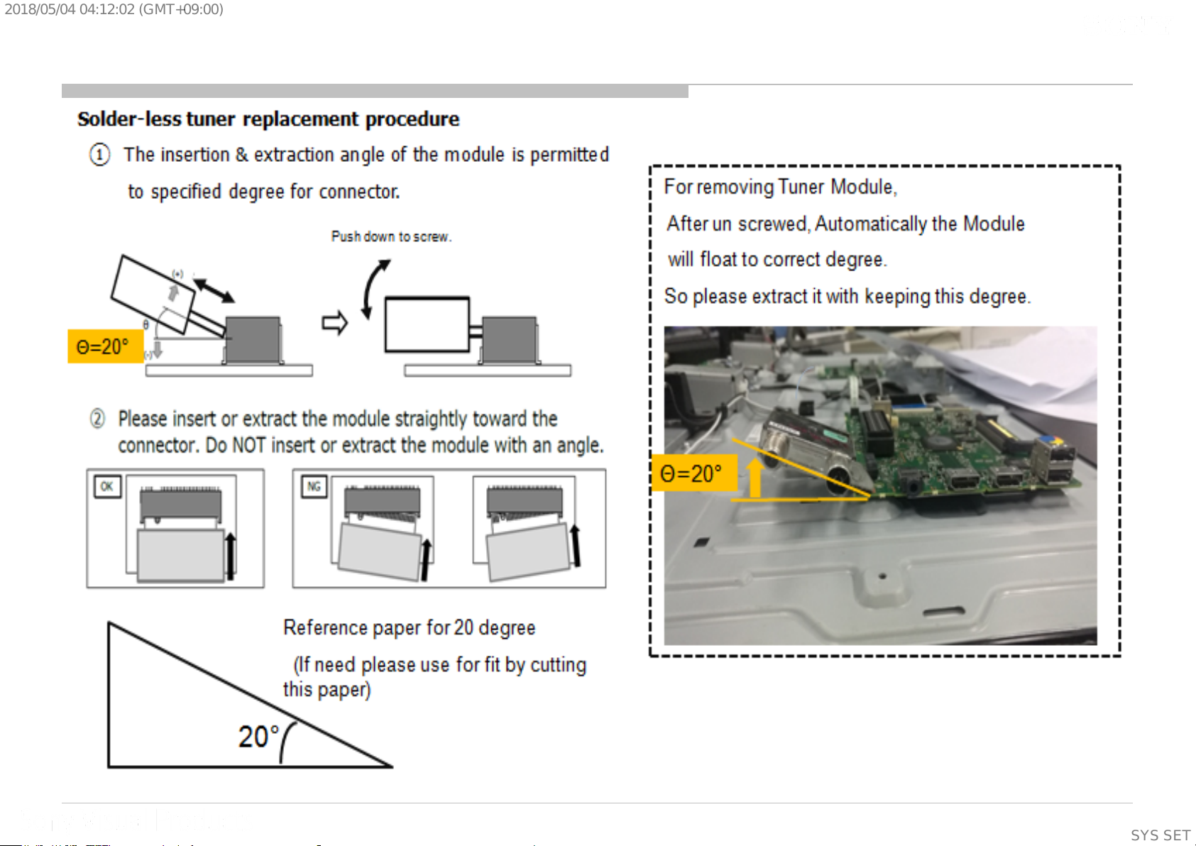
1-9. Solder-less Tuner Replacement
11
SYSSET
Page 12
2018/05/0404:12:02(GMT+09:00)
The units i n t his m anual cont ain a self-diagno sti c function. If an error oc cur s , the Smart C or e R ed LED w i ll automatical l y begin to flash.
The number of times the LED flashes tr anslates to a probable sour ce of the problem .
A definition of the Smar t Core Red LED flash indi cators is listed in the instr uction manual for the user’ s knowledge and reference.
If an error symptom cannot be reproduc ed, the rem ote com mander can be used to review the failure oc curr ence data stored i n memory to
reveal past problems and how often these problems occur .
DIAGNOSTIC TEST INDICATORS
When an error occurs , the Smar t Cor e Red LED will flash a set number of times to indi cate the possi ble cause of the pr oblem.
If there is more than one err or, the LED wil l identify the first of the problem areas.
Result for all of the following diagnosti c item s are displ ayed on screen.
If the scr een di s play s a “0”, no er r or has occ ur r ed .
SECTION 2
SELF DIAGNOSTIC FUNCTION
Status
LED Colour
Remarks
LED Indicator
• Lights up in white when you select “Picture Off”.
• Lights up in amber when you set the timer or
“Photo Frame Mode”.
• Lights up in white when the TV is turned on.
• Flashes while the remote is being operated.
Amber = Red + Green
Power Off
( AC Off and *1)
Power On
Standby
( by remote control
off and Side Key
off)
Picture Off
Set "Sleep Timer"
Set "On Timer"
( Power On )
Set "On Timer"
( Standby )
Picture Frame
Failure
Error of panel ID
Software Updating
Software Updating
failure
OFF
White
OFF
White
Amber
Amber
Amber
Amber
Red Blinking
Amber / Green Blinking
Amber Blinking
Amber / Red Blinking
*1 power switch off (by
Side Key)
The number of LED
blinking indicates cause of
failure.
Blinking:0.5sec Amber/
0.5sec Green
Blinking: 1sec On / 1sec Off
Blinking:1 sec Amber/ 1sec
Red
12
SYSSET
Page 13

2018/05/0404:12:02(GMT+09:00)
Failure LED Display
The Number of Standby LED
(RED blinking)
2 Main Power Error
3 Audio Error Main Board
4 Panel Power Error Main Board
5 Panel I2C Communication Error Main Board or Source Board
6 Backlight Error Main Board
Error Detection Error Location
AC Adaptor or Power Supply
Unit
Tuner Demod Error do not go to Safety Shutdown and do not have RED blinking.
Error Detection Symptoms Error Location
Tuner Demod Error Cannot tune Digital RF/ Analog RF Main Board/Tuner Module
13
SYSSET
Page 14
Before you make the service call…
1. Confirm the symptom from the customer.
2. Select that symptom from the chart.
3. Bring all the boards and cables listed for that symptom .
4. Follow the troubleshooti n g charts in the technical guides to isolate the board.
5. Chart
RED
BLUE
BLACK
No White Power
LED & does not
Stationary
dots
2018/05/0404:12:02(GMT+09:00)
Triage Char t
Colour Code
DOT: Most likely defective part
TRIANGLE: Secondary possible defective part
TEXT: Board that may correct the symptom
SECTION 3
TROUBLESHOOTING
Symptoms - Shutdown. Power LED
blinking red diagnostics sequences
No
Power
Reference
2 3 4 5 6
B* Board
G* Board
H* Board
Speaker
Wifi Module
LD* Board
VBO FFC
Tcon/Source
Board
LCD Panel
Problem
Power Power
Audio
LD
Panel
(Communication)
Panel
(Backlight)
reponse to
remote (Dead
Set)
- missin g or distorte d
colored
lines o r
Video
No video
One of
Inputs
No video
all Inputs
Remote Network Audio Smart Core
No Remot e
Wireless
can't connect
No Audio
Smart Core no LED
(Se t is still a liv e)
14
SYSSET
Page 15
2018/05/0404:12:02(GMT+09:00)
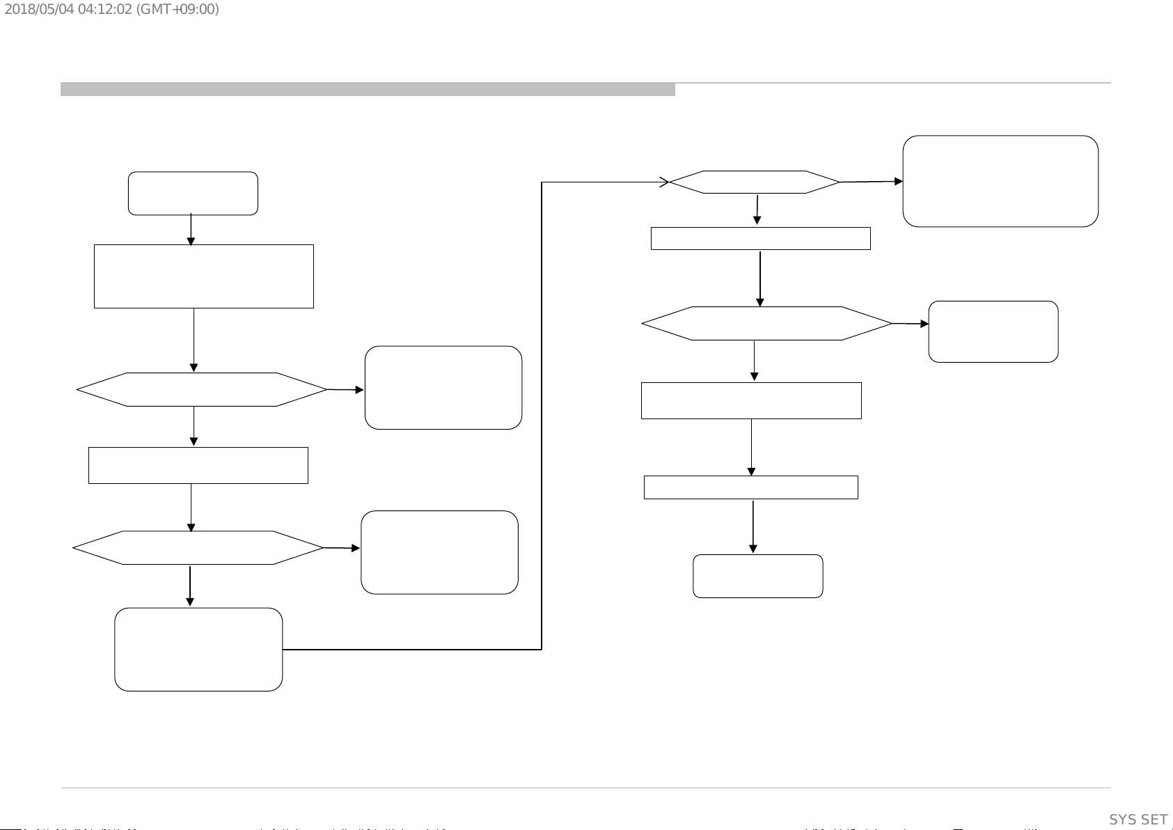
3.1 No power - LD board
START
LD board
1. Check fuse imped a n ce
F1001
Is < 1ohm ?
yes
2. Check impedance
D1001 to GND
Is > 1kohm?
yes
3. Check MOSFET
Q1007
Is > 1kohm?
yes
4. Check MOSFET
Q1002
Is > 1kohm?
yes
5. Check MOSFET
Q1008
Is > 1kohm?
no
no
no
no
no
Fuse F1001 broken
Diode D1001 broken
MOSFET Q 1007 Brok en
MOSFET Q 1002 Brok en
MOSFET Q 1008 Brok en
2
Q1007
3
4
F1001
D1001
1
Q1002
5
Q1008
yes
Check B board
15
SYSSET
Page 16

2018/05/0404:12:02(GMT+09:00)
3.1 No power - LD board
12V DDCON check
START
Check fuse F1000
Is < 1ohm
yes
Check Input to GND
Is > 1k ohm?
yes
Check Input to Output
Is > 1k ohm?
yes
Check Output to GND
Is > 1k ohm?
yes
Check 12V
C1016 voltage
Is voltage <12V?
yes
Check EN POWER_ON
R1003 voltage
Is voltage >2.5V?
yes
Check Vcc
C1009 voltage
Is voltage >5.0V?
yes
no
no
no
no
≥ 12V
no
no
Fuse F1000 broken
DDC IC1000 broken
DDC IC1000 broken
DDC IC1000 broken
Check B-Board
Troubleshooting flow 1.2
IC1000 broken
12V_TCON check
yes
Check 12.5V_TCON
Is voltage > 12.0V?
no
Check TCON_O N
C1024
Is voltage > 3.0V?
yes
Check MOSFET
Q1006
Is > 1kohm?
yes
12V power OK
Check other troubleshooting flow
END
no
no
Main device failure
Q1006 broken
Check point on PWB refer next slide
16
SYSSET
Page 17
2018/05/0404:12:02(GMT+09:00)
3.1 No power - LD board
Input t o G N D
Impedance check
C1024
+12.5V_TCON
Input t o O ut put
Impedance check
C1016
F1000
R1003
C1009
Q1006
Impedance check
Output to GND
Impedance check
17
SYSSET
Page 18

2018/05/0404:12:02(GMT+09:00)
3.2 LED Blink ing: 2x (Main power E rror - Operating Chart )
BB9(G* Board mode l) BB9(AC adapter model)
23V
13.2V
12.2V
16.44V
18
SYSSET
Page 19
2018/05/0404:12:02(GMT+09:00)
3.2 LED Blink ing: 2x (Main power E rror)
BB9(G* Board model)
2-time blinking
Check “+19.5_12.5V_MAIN”
at pin 15/16 of CN 5500
on BB9 Board,
Voltage 12.2V -13.2V?
*Typical 12.7V*
No
Yes
G* Board
BB9(AC adapter model)
2-time blinking
Check “+19.5_12.5V_MAIN”
at pin 15/16 of CN 5500
on BB9 Board,
Voltage 16.44V – 23V ?
*Typical 19.5V*
No
Yes
LD Board
BB9 Board
BB9 Board
19
SYSSET
Page 20
2018/05/0404:12:02(GMT+09:00)
3.2 : 2x Blinking – Main Power Error
LD Board
2 times
Blinking
LD-Board
Check DC voltage at
Q1002
18V – 20V?
*Typical: 19.5V
Yes
Change LD-
board
No
Adaptor
Take out adaptor
and check the output voltage.
18V – 20V?
(Refer Figure 1)
*Typical: 19.5V
Yes
Change LD-
Board
No
Change
Adaptor
-ve
+ve
Ensure that +ve
probe is touching
the needle.
Figure 1: How to check adaptor’s output voltage.
TV Business Division
(Supplementary
information)
20
SYSSET
Page 21
2018/05/0404:12:02(GMT+09:00)
Check point LD1
Board
Name
LD1
(Q1002)
Board PWB (A side) Detail
Q1002
19.5V
(Supplementary
information)
21
SYSSET
Page 22
2018/05/0404:12:02(GMT+09:00)
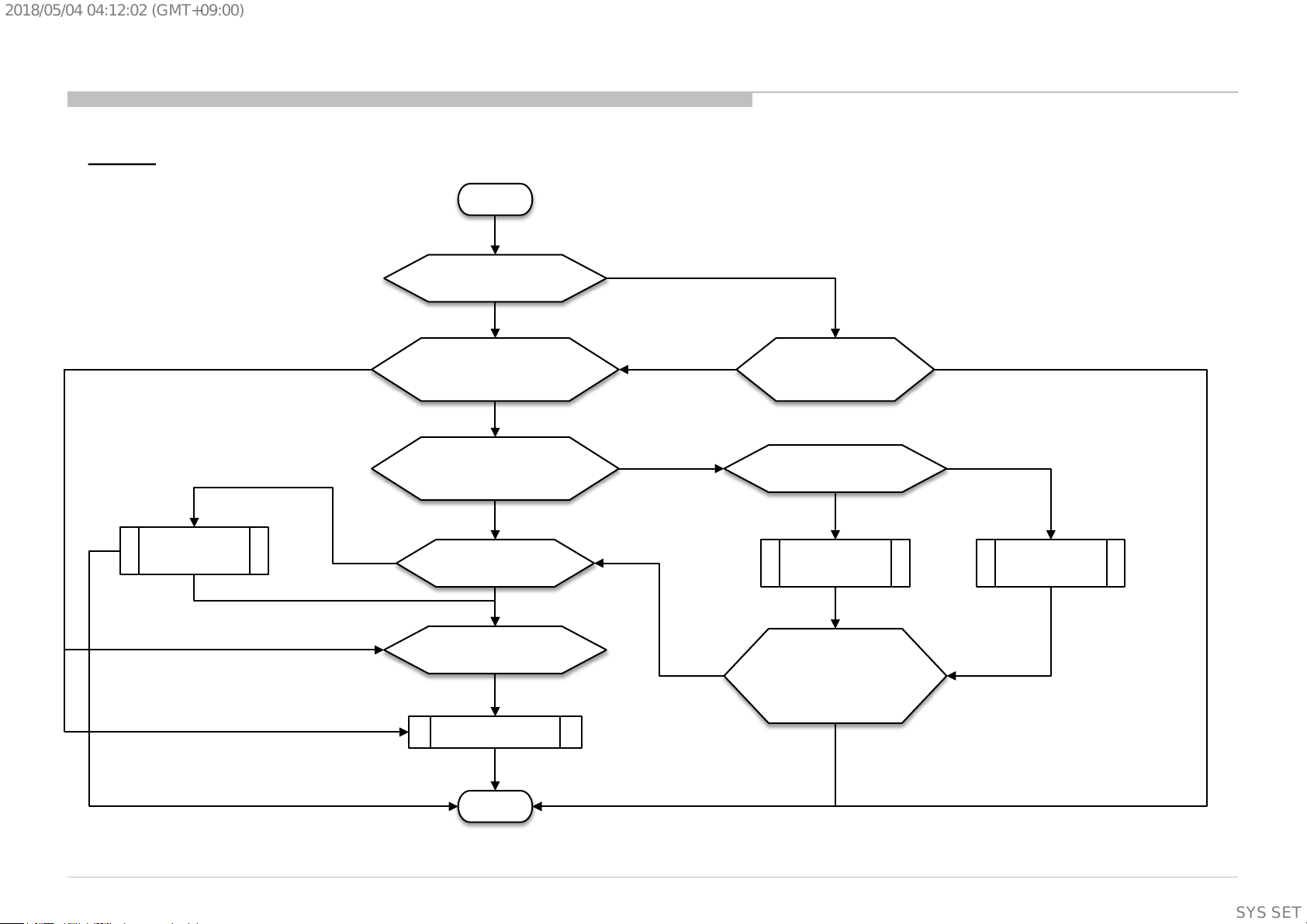
3.3 : 3x Blinking – Audio Error
B Board
B-board Audio Error pin
short to GND
No connectivity of F3101
F3101 broken,
Replace F3101
3x blinking & F3101 OK
START
3x blinking
Check correct Option bit is set?
Correct Option bit & 3x blinking
Disconnect pow er supply
and check Aud i o E rror p i n
Audio Error pin no short to GND
Remove Speaker Connecto r
at CN3109 and
perform AC OF F - ON
3x blinking
Check connecti vit y
of F3101
3x blinking & F3101 OK
Wrong Option bit
3x blinking
No 3x blinking
3x blinking
Important Note :
TV must be power OFF condition before
plug or unplug any of the
FFC/FPC/wire/cable from the board. ->
This is to prev en t possib ili ty c ir cu it
damage happen.
Set correct Option bit and
perform AC OF F - ON
Check Speaker harnes s and
Speaker impedance
Speaker harness
shorted
Change Speaker
Harness
No 3x blinking
Main Speaker
Impedance ≠ 6~8 Ω
Change Main
Speaker
No 3x blinking
#Audio IC (IC3101) problem
Change B-board
DONE
Connect back
Speaker Connector
to CN3109 and
perform AC OF F - ON
No 3x blinking
(Supplementary
information)
22
SYSSET
Page 23

2018/05/0404:12:02(GMT+09:00)
3.3 : 3x Blinking – Audio Error
B Board
(#Audio I C (I C 3 101) problem)
START
#Audio IC (IC3101) problem
3x blinking and F3101 OK
Check Audio IC pins and surrounding part,
Replace the NG part if have any
(For example, fuse broken, e.capacitor blow,
c.capacitor short connection,
inductor open connection and etc.)
3x blinking
Check have any burn mark on Audio IC,
If have burn mark, replace the NG Audio IC
Important Note :
TV must be power OFF condition before
plug or unplug any of the
FFC/FPC/wire/cable from the board. ->
This is to prev en t possib ili ty c ir cu it
damage happen.
No 3x blinking
No 3x blinking
3x blinking
Change B-board
DONE
(Supplementary
information)
23
SYSSET
Page 24
2018/05/0404:12:02(GMT+09:00)
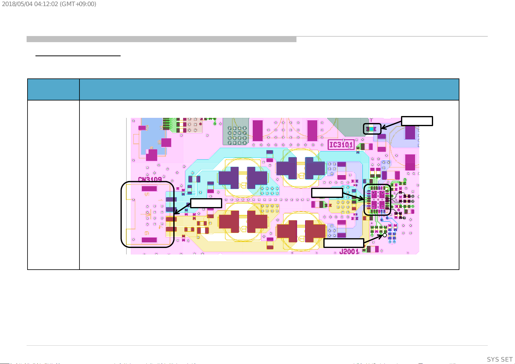
3.3 : 3x Blinking – Audio Error
B Board (Checking Point)
Board PWB
(A side)
Purpose :
Checking Audio
Error pin not
short to GND
Checking fuse
condition
Change Audio IC
if need
Audio IC each pin
checking, please
refer to “Audio
No Sound”
BB9 (CHL) - Audio A mp circuit
F3101
IC3101
CN3109
Audio Erro r pi n
(Supplementary
information)
24
SYSSET
Page 25
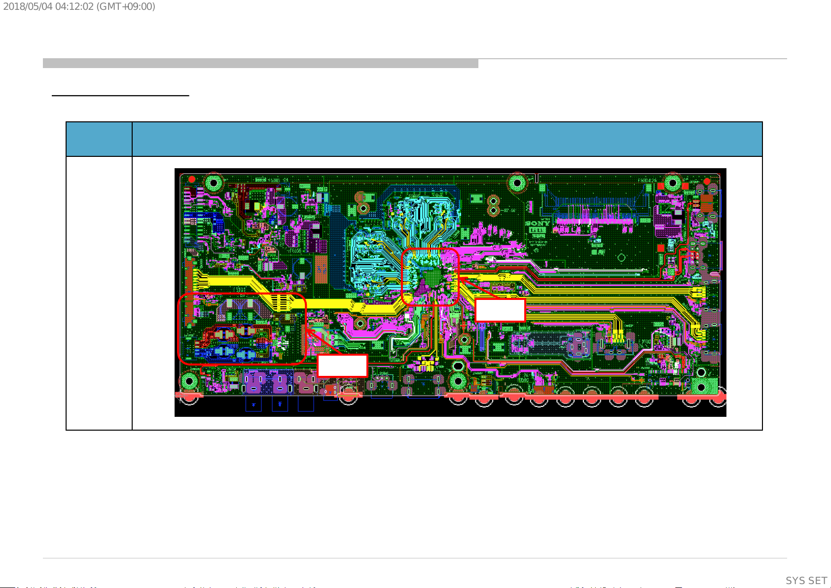
2018/05/0404:12:02(GMT+09:00)
3.3 : 3x Blinking – Audio Error (Back up)
B Board (Checking Point)
Board PWB
(A side)
BB9 (CHL)
Main IC
(IC5000)
Audio Amp
circuit
(Supplementary
information)
25
SYSSET
Page 26
2018/05/0404:12:02(GMT+09:00)
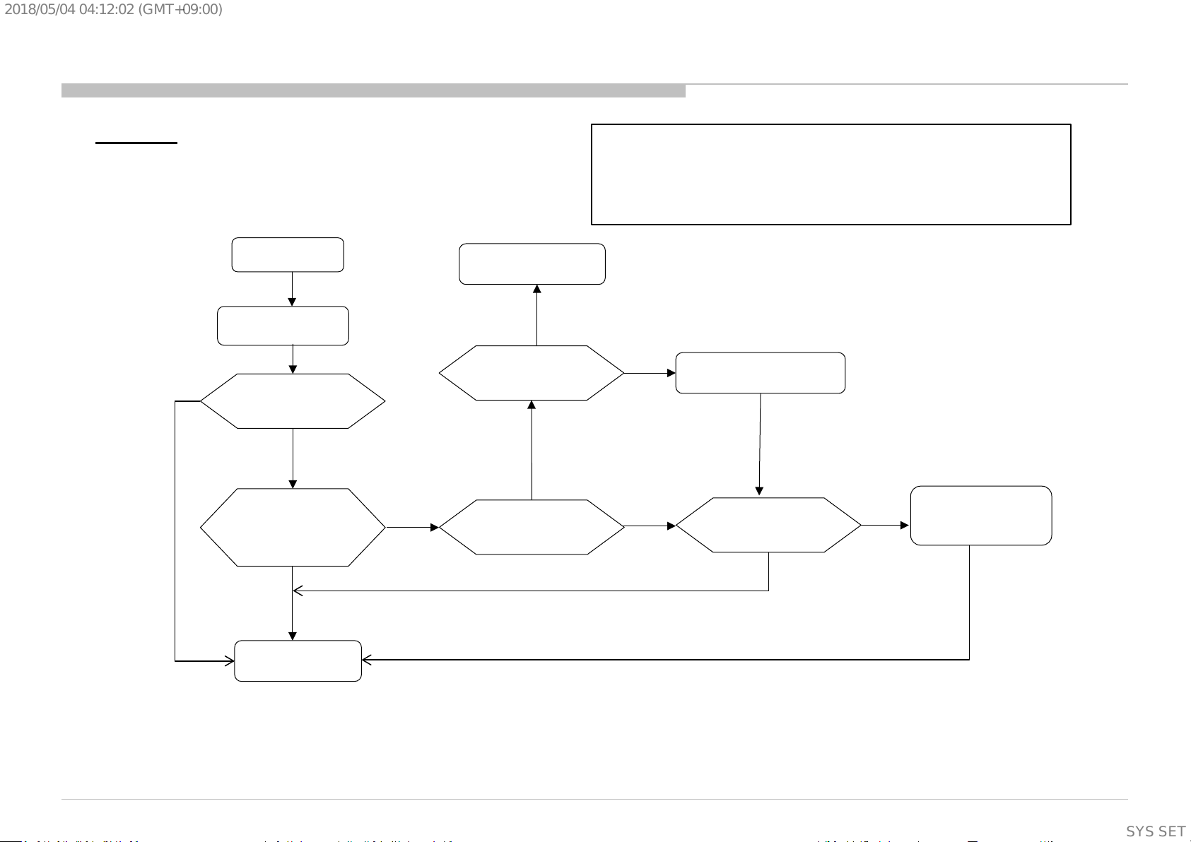
3.4 : 4x Blinking – Panel Power Error
BB9 Board
Yes
Start
*Check Adaptor /
G board connection
TV boot up normally?
No
Check voltag e at
+12.5V_TCON
10.8V-13.2V
No
RC ON
Yes
TV in standby mode?
No
Check PANE L_PWR
3.00V-3.33V?
*Check Adaptor / G-board connection
CHL 43/49 = LD board & Adaptor
CHL 55/65 = G-board
Adaptor: Remove and reinsert Harness from LD board Main board
G-board: Remove and reinsert Harness from Gboard Main board
No
Replace Main IC / B-Board
Yes
Check +12.5V_TCON
10.8V-13.2V?
No
Suspected LD board / G
Board side issue.
Replace PSU uni t board
Yes
End
(Supplementary
information)
26
SYSSET
Page 27
2018/05/0404:12:02(GMT+09:00)
BB9 layout
30pin PSU/LD
Connector
51pin LVDS C onnec tor
SoC
+12.5V_TCON
TV Business Division
PANEL_PWR
27
SYSSET
Page 28
2018/05/0404:12:02(GMT+09:00)
3.5 : 5x Blinking – P anel I2C Error
START
Reinsert LVDS 51pin Flat
Flexible Cable (FFC) at B-Boar d and
Panel Side. Make sur e F FC is t aped
properly.
5 Times Blinking happen?
YES
Replace LV DS 51 pin Flat Flexible
Cabl e (FFC )
5 Times Blinking happen?
YES
No
No
TV set is OK now
NG Symptom:
Incorrect FFC Ins ertion
TV set is OK now
NG Symptom:
LVDS Cable NG
Is 10.8 – 13. 2V available?
YES
Replace B-Board
5 Times Blinking happen?
YES
Replace
O-Cell* or Panel M odule*
TV Boots Up Normally
END
NO
TV set is OK now
NG sympton:
LD board/ G board
no +12.5V_TCON supply
No
TV set is OK now
NG Symptom:
B-Board Is su e NG
* O-Cell or Panel
Module replacement
depends on ser v ice
capabilities
Check voltage at +12.5V_T CO N
28
SYSSET
Page 29
2018/05/0404:12:02(GMT+09:00)
BB9 layout
30pin PSU/LD
Connector
51pin LVDS C onnec tor
SoC
+12.5V_TCON
29
SYSSET
Page 30
2018/05/0404:12:02(GMT+09:00)
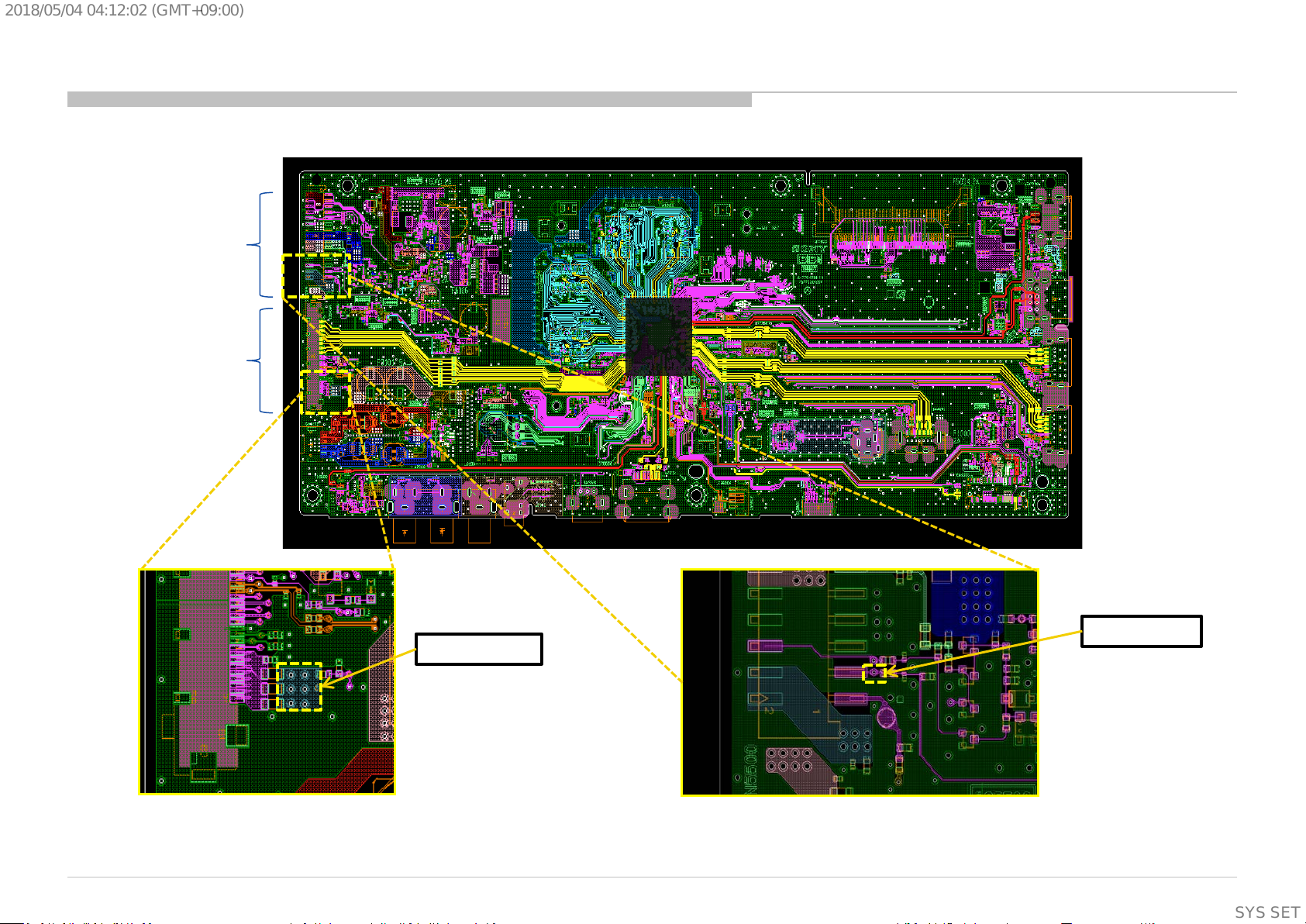
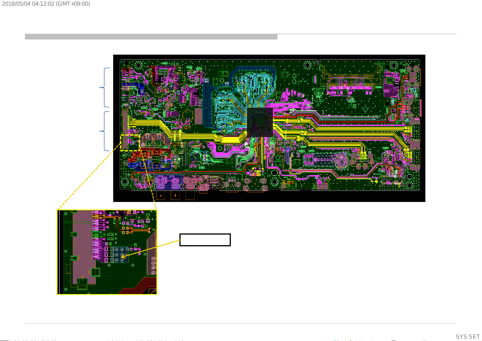
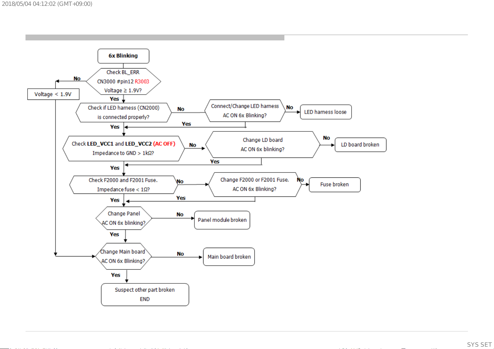
3.6 6x Blinki ng back l ight error
Check point on PWB refer next slide
30
SYSSET
Page 31

2018/05/0404:12:02(GMT+09:00)
3.6 6x Blinking backlight error
31
SYSSET
Page 32

2018/05/0404:12:02(GMT+09:00)
3.7 Blank Screen, Backlight Visible
No Picture
Got Any Abnormal
Display?
Yes
Check Other
Portion:
Tuner - No Picture
Check Smart Core
LED Indication
No
Troubleshoo ting manual
Ext. Video Input -
No Picture
HDMI - No Picture
(5x Blinking)
Refer 5x Blinking
Yes
No
Replace
the V by One FFC
Harness
OK
V by One FFC
Harness NG
NG
Replace
the main Board
OK
Main board NG
NG
Replace
LD/G Board
NG
LCD Panel
(T-CON) NG
OK
LD/G Board NG
32
SYSSET
Page 33

2018/05/0404:12:02(GMT+09:00)
3.8.1 NO PICTURE: TUNER (for Analogue , Digital and Satel li te)
RF input no picture / noisy picture
Check RF source cable
and antenna, OK?
OK
Check Tuner power line:
3.3V at CL1000 = 3.3V?
1.8V at CL1001= 1.8V?
OK
Tuning for Analog, Dig ital or
Satellite?
NG
NG
Change RF cable and antenna
For 1.8V Please refer DDCON
troubleshooting (2a)
For 3.3V Please refer DDCON
troubleshooting ( 2a)
Satellite
NG
Check fuse F1000 continuity.
Part broken?
YES
Change part
F1000
Problem solved?
NG
Change Tuner Module EU-T2S2
(SUT-CE251ZP)
(Please refer page Assemble and
Dissemble Tuner Module)
Please refer DDCON 12V LNB
Voltage troubleshooting (2a)
NO
OK
Done (End)
Refer Analog Tuning
Digital
For TW-DVB ,
AM-ATSC, LA-ISDB & EUDVB only.
Refer Digital Tun ing 1
Check Tuner power line
12V line at CL1006 = 12V?
OK
For EU-T2S2, PA-T2,
HK-DTMB, LA-T2
& PA-ISDB only.
Refer Digital Tun ing 2
Problem solved?
NG
Change B-board
OK
Done (End)
33
SYSSET
Page 34
2018/05/0404:12:02(GMT+09:00)
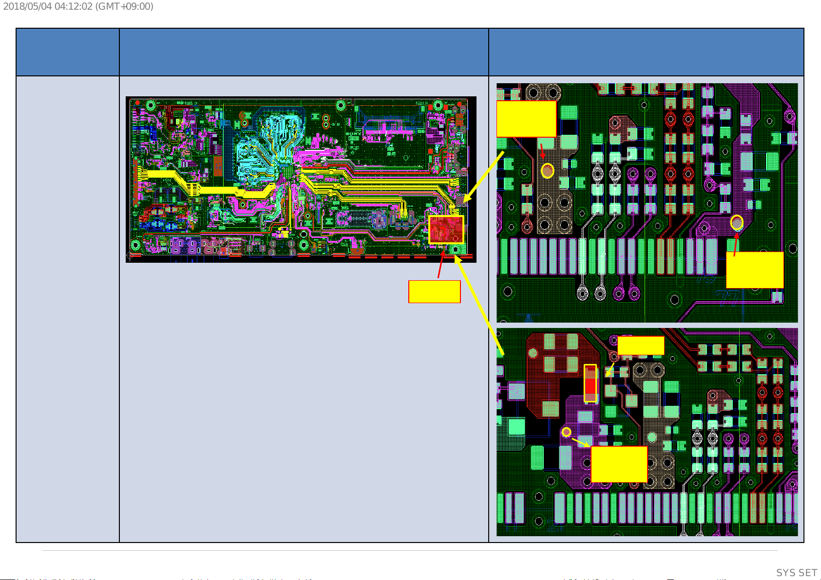
Board Name Board PWB (A side) Detail
BB9 board
(A side)
(3.3V)
CL1000
(1.8V)
CL1001
(12V)
CL1006
F1000
BB9 board
(A side)
CL1001
(1.8V)
CL1000
(3.3V)
Detail
F1000
CL1006
(12V)
(Supplementary
information)
34
SYSSET
Page 35

2018/05/0404:12:02(GMT+09:00)
3.8.2 For Anal ogue Tuning Failed ( All destination)
Analog Tuning
For Other
destination
Channel can be lock?
OK
Picture quality is noisy?
Not Noisy
Noisy
NG
For LA-ISDB,
PA_ISDB &
LA-T2
Confirm Antenna or Cable connection
Check part mounting condition for
digital control line
“M_SCL,M_SDA”
OK
Check part mounting condition
for analog control line
“IFOUTN1, IFOU TP1,
IFAGC1”
OK
Notes:
- Parts for IFOUTN1 line: FB1000,C1005,C1012
- Parts for IFOUTP1 line: R1030, FB1001, C100 6,C10 13
- Parts for IFAGC1 line: C1014, R1010
-Parts for M_SCL line: C1004,R1049
-Parts for M_SDA line: C1003,R1048
NG
NG
Done (End)
OK
Please r e-
upgrade
Firmware (PK G),
Check again
Picture quality?
NG
Change Tuner Module
(Please refer page Assemble and Dissemble Tuner Module)
OK
Problem solved?
NG
Change B-board
35
SYSSET
Page 36

2018/05/0404:12:02(GMT+09:00)
Board Name Board PWB (A side) Detail
BB9 board
(A side)
(IFOUTN1)
FB1000
C1005
C1012
(IFOUTP1)
R1030
FB1001
C1006
C1013
C1012
C1006
C1005
FB1001
R1030
FB1000
C1013
36
SYSSET
Page 37

2018/05/0404:12:02(GMT+09:00)
Board
Name
BB9 board
(A side)
(IFAGC1)
C1014
R1010
Board PWB (A side) Detail
C1014
R1010
37
SYSSET
Page 38

2018/05/0404:12:02(GMT+09:00)
Board
Name
BB9 board
(A side)
(M-SCL)
C1004
R1049
(M-SDA)
C1003
R1048
Board PWB (A side) Detail
R1049
C1004
C1003
R1048
38
SYSSET
Page 39

2018/05/0404:12:02(GMT+09:00)
3.8.3 FOR DIGITAL TUNING 1: For TW-DVB , AM-ATSC,LA-ISDB , EU-DVB only
Digital Tuning 1
Notes:
- Parts fo r IFOUTN1 line: FB1000,C1005,C1012
- Parts for IFOUTP1 line: R1030,
FB1001,C1006,C1013
- Parts fo r IFAGC1 line: C1014, R1010
-Parts for M_SCL line: C1004,R104 9
-Parts for M_SDA line: C1003 ,R10 48
Channel can be lock?
OK
OK (but no picture)
Sound is normal?
No sound
Confirm UEC of digital RF by Service mode
If UEC > 0
Check part mounting conditio n for digital data line
“IFOUTN1, IFOUTP1, IFAGC1”
OK
Please re-upgrade Firmware (PKG),
Check again Picture quality?
OK
NG
If UEC = 0
NG
NG
Check part mounting conditio n for
digital control line
“M_SCL,M_SDA”
OK
Check IC 5000(SoC)
(Change B-board)
Change NG parts
(Please refer page Assemble and Dissemble Tuner Module)
NG
Change NG parts
Problem
solved?
NG
Change Tuner Module
OK
Done (End)
Done (End)
OK
Problem solved?
NG
Change B-board
39
SYSSET
Page 40

2018/05/0404:12:02(GMT+09:00)
Board
Name
BB9 board
(A side)
(IFOUTN1)
FB1000
C1005
C1012
(IFOUTP1)
R1030
FB1001
C1006
C1013
Board PWB (A side) Detail
C1012
C1006
C1005
FB1001
R1030
FB1000
C1013
40
SYSSET
Page 41

2018/05/0404:12:02(GMT+09:00)
Board
Name
BB9 board
(A side)
(IFAGC1)
C1014
R1010
Board PWB (A side) Detail
C1014
R1010
41
SYSSET
Page 42

2018/05/0404:12:02(GMT+09:00)
Board Name Board PWB (A side) Detail
BB9 board
(A side)
(M-SCL)
C1004
R1049
(M-SDA)
C1003
R1048
R1049
C1004
C1003
R1048
42
SYSSET
Page 43

2018/05/0404:12:02(GMT+09:00)
3.8.4 FOR DIGITAL TUNING 2: For EU-T2S2, PA-T2, LA-T2 ,HK-DTMB & PA-ISDB only.
Digital Tuning 2
For LA-T2 For EU-T2S2
Confirm ANT or Cable connection
Channel can be lock?
Sound is normal?
No sound
Confirm UEC of digital RF by Service mode
If UEC > 0
Check part mounting conditio n for digital data line
“DEMOD_TSCL K, DEMOD_TS DATA”
OK
For EU-T2,
PA-T2,
and HK-DTMB
Confirm ANT or Satellite connection
NG
OK
If UEC = 0
Check part mounting conditio n for
NG
digital control line
“M_SDA,M_SCL”
5000(SoC)
(Change B-board)
Change NG parts
NG
Check IC
Notes:
-Parts for M_SCL line: C1004,R1049
-Parts for M_SDA line: C1003,R1048
-Parts for DEMOD_TSCLK line: R1020
- Parts for DEMOD_TSDATA line: R1019
OK
Change NG parts
Problem
solved?
OK
Done (End)
OK
Please re-upgrade Firmware (PKG),
Check again Picture quality?
OK
OK
Done (End)
NG
NG
Change Tuner Module
(Please refer page Assemble and Dissemble Tuner Module)
Problem solved?
NG
Change B-board
43
SYSSET
Page 44
2018/05/0404:12:02(GMT+09:00)
Board
Name
BB9 board
(A side)
(M-SCL)
C1004
R1049
(M-SDA)
C1003
R1048
Board PWB (A side) Detail
R1049
C1004
C1003
R1048
44
SYSSET
Page 45

2018/05/0404:12:02(GMT+09:00)
Board Name Board PWB (A side) Detail
BB9 board
(A side)
(DEMOD_TSCLK)
R1020
(DEMOD_TSDATA
0)
R1019
R020
R1019
45
SYSSET
Page 46

2018/05/0404:12:02(GMT+09:00)
3.8.5 EWBS – (for PA-ISDB Only)
If TV unable to output audible tone /wakeup during standby after received EWBS signal– General Checking
Start
Connection Failed
Check region settin g
OK
NG: Wrong region
setting
TV does not triggered
Due to region
Miss matched
EWBS UI: ON
OK
Does any
RF signal stored
from RF Antenna?
OK
Does Tuning RF
Antenna
OK?
OK
Check mount
Part at EWBS lin e
R5066
OK
NG: Tuner power is OFF
NG: Tuner power is OFF
NG: Cannot locked
any signals
NG: Part missing
EWBS Feature is
Not Enable
During standby
EWBS Feature is
Not Enable
during standby
Refer to
2f.3.1 No Picture Tuner
Trouble shooting
flow
Replace board
END
(Supplementary
information)
46
SYSSET
Page 47

2018/05/0404:12:02(GMT+09:00)
3.8.6 – NO SOUND
No Sound with normal picture
NO
Only RF tuner input?
YES
Change B-board
Please refer Aud io
troubleshooting
(Supplementary
information)
47
SYSSET
Page 48
2018/05/0404:12:02(GMT+09:00)
3.9.1 USB Port 1
3.9.1 USB Port 1– No Detection / Cannot Play / No pict ur e / N o Sound – General Checki ng
TV turn ON condition:
START
Do a Fac t or y S et ti ng
Chan ge t o ON
Detec ti on OK
and
Picture and Sound O K
OK
OFF
NG
*1 Confirm USB Auto Start is
ON or OFF
ON
Check 5V at C7012
(USB port1)
Have 5 V bu t No d et ec ti o n
*2 Confirm U SB file
format
OK
NG
Change to supported USB format
Remarks:
*1 Confirm USB AutoStart at Set-up Menu.
*2 Confirm with OSD on bottom pane l, if
playback not suppor t.
Please refer to IM for detail supported U SB
format.
No 5V
Detec ti on OK
OK
Picture OK
OK
Sound OK
OK
END
US B for m at OK b u t N o detec ti on
Picture NG
Main IC (IC 5000) problem
Sound NG
Audio IC (IC3101) problem
Chan ge B-Board
(Supplementary
information)
48
SYSSET
Page 49

2018/05/0404:12:02(GMT+09:00)
3.9.2 USB Port 2
3.9.2 USB Port 2– No Detection / Cannot Play / No pict ur e / N o Sound – General Checki ng
TV turn ON condition:
START
Do a Fac t or y S et ti ng
Chan ge t o ON
Detec ti on OK
and
Picture and Sound O K
OK
OFF
NG
*1 Confirm USB Auto Start is
ON or OFF
ON
Check 5V at C7029
(USB port2)
Have 5 V bu t No d et ec ti o n
*2 Confirm U SB file
format
OK
NG
Change to supported USB format
Remarks:
*1 Confirm USB AutoStart at Set-up Menu.
*2 Confirm with OSD on bottom pane l, if
playback not suppor t.
Please refer to IM for detail supported U SB
format.
No 5V
Detec ti on OK
OK
Picture OK
OK
Sound OK
OK
END
US B for m at OK b u t N o detec ti on
Picture NG
Main IC (IC 5000) problem
Sound NG
Audio IC (IC3101) problem
Chan ge B-Board
(Supplementary
information)
49
SYSSET
Page 50

2018/05/0404:12:02(GMT+09:00)
3.9.3 USB Port 3
3.9.3 USB Port 3– No Detection / Cannot Play / No pict ur e / N o Sound – General Checki ng
TV turn ON condition:
START
Do a Fac t or y S et ti ng
Chan ge t o ON
Detec ti on OK
and
Picture and Sound O K
OK
OFF
NG
*1 Confirm USB Auto Start is ON
or O FF
ON
Check 5V at C7037
(USB port3)
Have 5 V bu t No d et ec ti o n
*2 Confirm U SB file
format
OK
Detec ti on OK
OK
Picture OK
Change to supported USB format
US B for m at OK b u t N o detec ti on
Remarks:
*1 Confirm USB AutoStart at Set-up Menu.
*2 Confirm with OSD on bottom pane l, if
playback not suppor t.
Please refer to IM for detail supporte d USB
format.
No 5V
NG
Picture NG
OK
Sound OK
OK
END
Sound NG
Main IC (IC 5000) problem
Audio IC (IC3101) problem
Chan ge B-Board
(Supplementary
information)
50
SYSSET
Page 51

2018/05/0404:12:02(GMT+09:00)
3.9.4 USB Port 1 or 3
3.9.4 USB Port 1 or 3 – No D etect ion / Cannot Play / No pi c tur e / N o Sound – Checking Point
USB ( B -board Checking) – Checking 5V Points [USB Port 1 or 3]
Board
Name
BB9
Board PWB (A side) Detail
Have 5V?
C7012
C7037
(Supplementary
information)
51
SYSSET
Page 52

2018/05/0404:12:02(GMT+09:00)
3.9.5 USB Port 2
3.9.5 USB Port 2 – No Detection / Cannot Play / N o pictur e / N o Sound – Checking Point
USB ( B -board Checking) – Checking 5V Points [USB Port 2]
Board
Name
BB9
Board PWB (A side) Detail
Have 5V?
C7029
(Supplementary
information)
52
SYSSET
Page 53

2018/05/0404:12:02(GMT+09:00)
3.10 Ethernet
3.10 Ethernet – No Connect – General Checking
TV turn ON condition:
START
Check if TV has good
cab le conn ecti on
Set-up Network setup
Failed
Check if the Ethernet
cable is good
NG
Chan g e a good c ab l e
Check TV has connection O K
Set-up Network setup
OK
OK
OK
Failed
Check if any abnormal
or broken point on
Ethernet Connector and parts
(J7000/L7000/RB7000/C7002)
No
Check if TV has MAC Address
Set-up Network setup
Failed
Invalid MAC Address
Chan ge B Boar d
Yes
Yes
Connector (J 7000) and parts N G
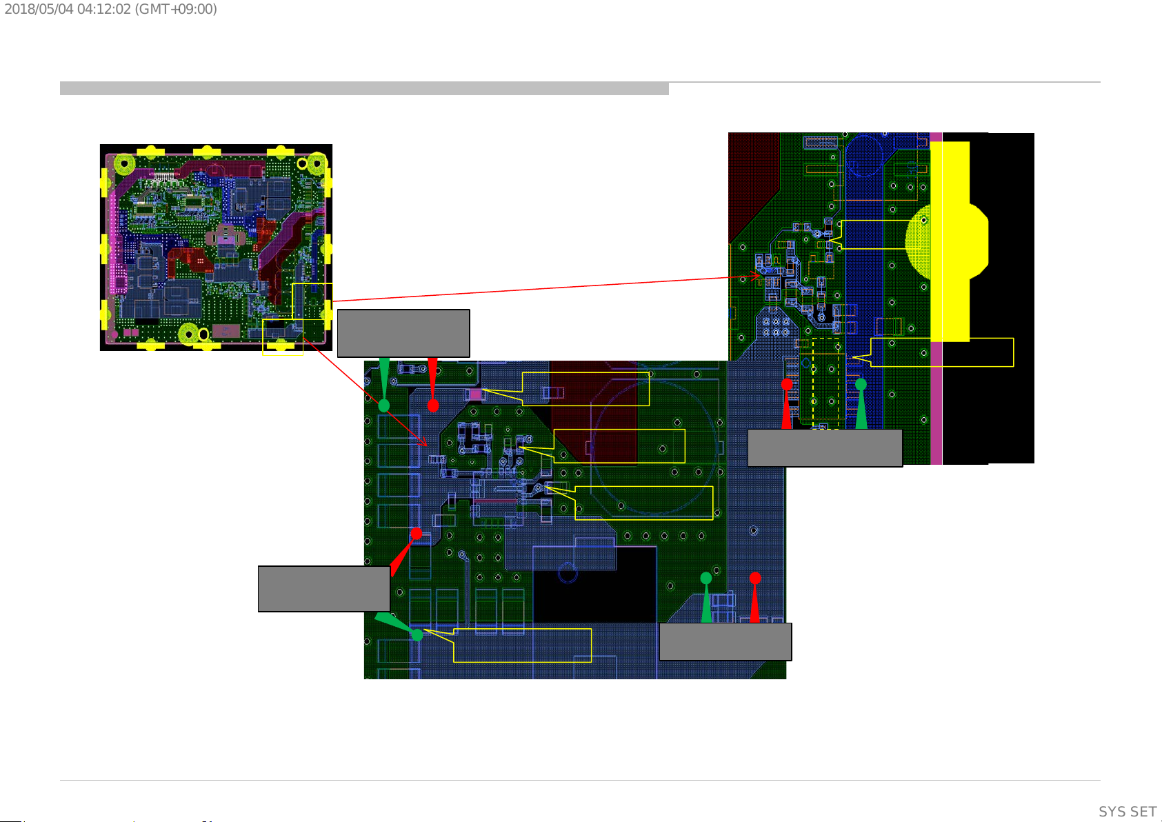
Chan ge B Boar d
T7000 or T7001 or Main IC (IC5000)
NG
Chan ge B Boar d
53
END
53
SYSSET
Page 54

2018/05/0404:12:02(GMT+09:00)
3.10 Ethernet
3.10 Ethernet – No Connect – General Checking
Ethernet (B-board Che c k ing) – Checking parts broken or knock off
Board
Name
BB9
Board PWB (A side) Detail
Check any
parts broken
T7000
or knock off?
RB7000
C7002
L7000
T7001
J7000
54
SYSSET
Page 55

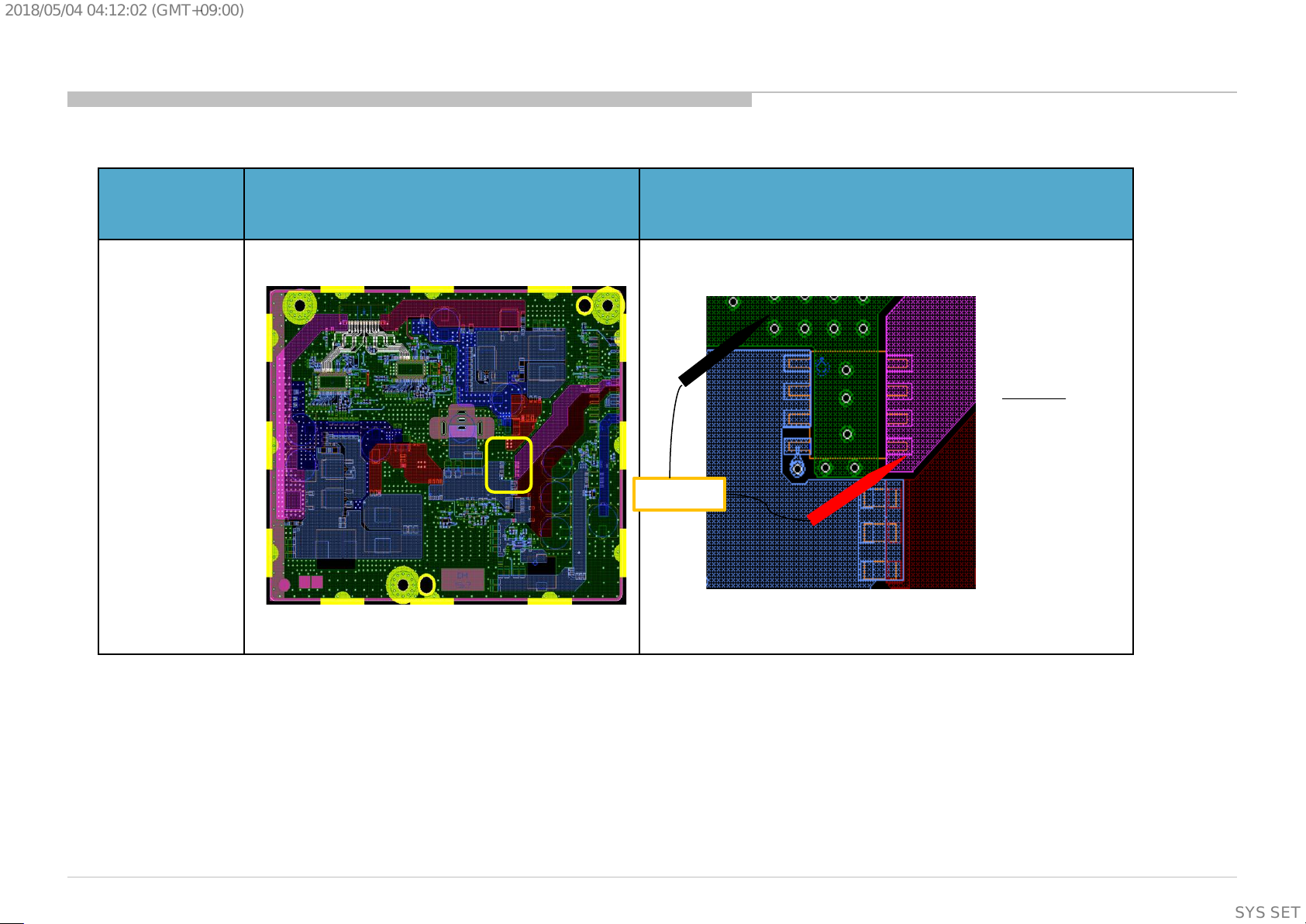
2018/05/0404:12:02(GMT+09:00)
3.11 CI Slot
3.11 CI Slot – Cannot Play / No picture / No Sound – General Checki ng
TV turn ON condition:
START
*1 Insert Good CICAM and
Check if TV can detect CICAM
Channel Setup Digital Setup
Yes
CA Module
No
No
Insert CICAM and
Check CI 5V
at PIN 17/18/51/52
Change B Board
Check CI or CI+ case
CI+
Check service menu for
CI+ Credentials CI+ Key
Invalid key
Invalid Key
Change B Board
CI
Valid key
Check any pin on
CI Slot is bend or
broken.
Connector NG
Change B Board
No
IC7003 NG
Remarks:
*1 Im por t an t : P leas e us e a kn own G ood C I C AM f or tes t in g
*2 Both CI Detection at Pin 36/67 s hould be 3. 3V before
CICAM insert and 0v when CICAM inserted.
*3 Con fi rm thes e 6 resi st ors par t are mou nt p roper l y.
Yes
Yes
*2 Insert CICAM and
Check CI Detection
at Pin 36/67
No
Yes
*3 Check Resistor
Part mounting
Yes
END
Power 3.3V NG
Change B Board
NG
Part Knock Off
Change B Board
Picture and
55
Sound OK
NG
Main IC (IC5000) NG
Change B Board
Yes
55
SYSSET
Page 56

2018/05/0404:12:02(GMT+09:00)
3.11 CI Slot
3.11 CI Slot – Cannot Play / No picture / No Sound – Checking Point
CI Slot (B-board Checking) – Checkin g 5V Point s [1/3]
Board
Name
BB9
Board PWB (A side) Detail
CI 5V at PIN
17/18/51/52
56
SYSSET
Page 57

2018/05/0404:12:02(GMT+09:00)
3.11 CI Slot
3.11 CI Slot – Cannot Play / No picture / No Sound – Checking Point
CI Slot (B-board Checking) – Checking CI Detection Pin Points [2/3]
Board
Name
BB9
Board PWB (A side) Detail
Card Detect 2 – PIN 67
Card Detect 1 – PIN 36
TV Business Division
Remark:
Both CI Detection Pin should be 3.3V before CICAM insert and 0 v when CICAM inserted.
(Supplementary
information)
57
SYSSET
Page 58

2018/05/0404:12:02(GMT+09:00)
3.11 CI Slot
3.11 CI Slot – Cannot Play / No picture / No Sound – Checking Point
CI Slot (B-board Checking) – Checking Resistor Part Mounting Points [3/3]
Board
Name
Board PWB (A side) Detail
BB9
Ref. No. Location Ref. No. Location
RB7003 1 RB7012 6
RB7004 2 RB7020 7
RB7005 3
RB7010 4
2
1
3
5
6
Remark:
Confirm these 6 resistors part are mount properly or not.
4
TV Business Division
(Supplementary
information)
58
SYSSET
Page 59

2018/05/0404:12:02(GMT+09:00)
Troubleshooting manual summary – No Picture
Section
3
Problem/Issue
No Picture
Symptom:
1. No Red LED
Blinking
2. White LED
3.12
3.12.1
3.12.2
3.12.3
3.12.4
3.12.5
3.12.6
HDMI No Picture
- HDCP Failure Analysis
- +5V Power Failure Analysis
- HPD Failure Analysis
- I2C Failure Analysis
- TMDS Failure Analysis
- Bravia Sync (CEC) not function- HDMI
Title
TV Business Division
(Supplementary
information)
59
SYSSET
Page 60

2018/05/0404:12:02(GMT+09:00)
3.12 HDMI No Picture
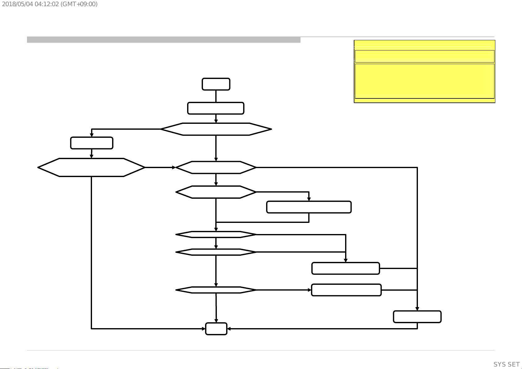
3.12 HDM I – No picture – General Ch ecking
HDMI No Picture
Verify with laptop /
Computer
[NG] No picture
Verify with other
HDMI player /cable
[NG] No picture
Factory reset
HDMI source & re-verify
[NG] No picture
Physical appearance check
On HDMI connector
[OK] Appearance OK
[OK] Picture recovered
[OK] Picture recovered
[OK] Picture recovered
[NG] Connector abnormal
[NG] No picture
Checking condition:
- TV ON & HDMI Source ON except if the flow men tione d is AC OFF.
- TV HDMI input connected to HDMI source (Player etc.)
- TV Input Selection: HDMI
Go to
"HDCP Failure Analysis“
Page
HDMI player/
cable problem
TV
setting problem
HDMI Connector Broken.
Replace & Re-verify
END
[OK] Picture recovered
Check voltage of +5V Power
HDMI1: CN4001 – Pin 18
HDMI2: CN4002 – Pin 18
HDMI3: CN4000 – Pin 18
[OK] V5V = 4.8 ~ 5.3V
Check voltage of HPD
HDMI1: CN4001 – Pin 19
HDMI2: CN4002 – Pin 19
HDMI3: CN4000 – Pin 19
[OK] V
HPD = 2.4 ~ 5.3V
Continue Next Page
TV Business Division
[NG] V
[NG] V
5V ≠ 4.8 ~ 5.3V
HPD ≠ 2.4 ~ 5.3V
Go to
“+5V Power Failure Analysis“
Page
Go to
“HPD Power Failure Analysis“
Page
(Supplementary
information)
60
SYSSET
Page 61

2018/05/0404:12:02(GMT+09:00)
3.12 HDMI No Picture
3.12 HDM I – No picture – General Checking (Continued)
Continue..
Check impedance of series
resistor at SCL&SDA during AC OFF
[OK] Impedance ≈ 100
[OK] VI2C = 3.5 ~ 5.5V
HDMI1: CN4001 – Pin1,3,4,6,7,9,10,12
HDMI2: CN4002 – Pin1,3,4,6,7,9,10,12
HDMI1: R4004 & R4007 (I2C)
HDMI2: R4005 & R4008 (I
HDMI3: R4003 & R4006 (I
Ω±5%
Check voltage o f SCL&SDA line
HDMI1: CN4001 – Pin 15 & 16
HDMI2: CN4002 – Pin 15 & 16
HDMI3: CN4000 – Pin 15 & 16
Check voltage of TMDS line
HDMI3: CN4000 – Pin1,3,4,6,7,
9,10,12
2C)
2C)
[NG] V
[NG] VTMDS ≠ 2.6 ~ 3.5V
[NG] Impedance ≠
100
Ω±5%
[NG] No picture
I2C ≠ 3.5 ~ 5.5V
Checking condition:
- TV ON & HDMI Source ON except if the flow men tione d is AC OFF.
- TV HDMI input connected to HDMI source (Player etc.)
- TV Input Selection: HDMI
Series Resistor Brok en.
Replace → Re-verify
Go to
“I2C Failure Analysis“
Page
Go to
“TMDS Failure Analysis“
Page
[OK] Picture recovered
END
[OK] V
TMDS = 2.6 ~ 3.5V
Replace B-board &
re-verify
Escalate this issue to
R&D team
TV Business Division
END
(Supplementary
information)
61
SYSSET
Page 62

2018/05/0404:12:02(GMT+09:00)
3.12 HDMI No Picture
3.12.1 HDC P Failu re Anal ysi s
Checking condition:
- TV ON & HDMI Source ON except if the flow men tione d is AC OFF.
- TV HDMI input connected to HDMI source (Player etc.)
- TV Input Selection: HDMI
HDCP
Failure Analysis
[OK] Compatible
Verify HDMI Source
device compatibilitie s for
HDCP version 2.2
[NG] Not Com pat i bl e
[NG] Not Com pat i bl e
HDMI Source incompatib le
for HDCP1.4 and HDCP 2.2
TV Business Division
Verify HDMI Source
device compatibilitie s for
HDCP version 1.4
[OK] Compatible
HDCP1.4 Issues
Replace B-Board and Re-verify
[OK] Pict ure recovered
END
HDCP2.2 Issues
[NG] No pict ure
HDCP key corrupted
Escalate this issue to
R&D team
(Supplementary
information)
62
SYSSET
Page 63

2018/05/0404:12:02(GMT+09:00)
3.12 HDMI No Picture
3.12.2 +5V Po w er Failure Analysis – HDMI1 and HDMI3
Checking condition:
- TV ON & HDMI Source ON except if the flow men tione d is AC OFF.
- TV HDMI input connected to HDMI source (Player etc.)
- TV Input Selection: HDMI
+5V Power
Failure Analysis
[OK] Impedance ≈ 1K Ω
[NG] Impedance ≠ 100kΩ ±5%
[OK] Picture recovered
Check impedance of
Resistor durin g AC OFF
HDMI1: R4025
HDMI3: R4024
Check impedance of
Varistor during AC OFF
HDMI1:
VR4010
HDMI3:
VR4009
Replace Broken Varistor
and Re-verify
END
[NG] Impedance ≠ 1K Ω
[NG] No picture
[OK] Impedance ≈ 100kΩ ±5%
[NG] No picture
Replace Broken Resistor
[OK] Picture recovered
and Re-verify
Go to
“HPD Power Failure Analysis“
Page
TV Business Division
(Supplementary
information)
63
SYSSET
Page 64

2018/05/0404:12:02(GMT+09:00)
3.12 HDMI No Picture
3.12.2 +5V Po w er Failure Analysis – HDMI2
Checking condition:
- TV ON & HDMI Source ON except if the flow men tione d is AC OFF.
- TV HDMI input connected to HDMI source (Player etc.)
- TV Input Selection: HDMI
+5V Power
Failure Analysis
Check impedance of
Resistor durin g AC OFF
HDMI2:
[OK] Impedance ≈ 22 Ω
Check impedance of
Varistor during AC OFF
HDMI2:
[NG] Impedance ≠ Open (High Z)
Replace Broken Varistor
and Re-verify
[OK] Picture recovered
R4044
VR4011
[NG] Impedance ≠ 22 Ω
Replace Broken Resistor
and Re-verify
[NG] No picture
[OK] Impedance ≈ Open ( Hi gh Z)
“HPD Power Failure Analysis“
[NG] No picture
[OK] Picture recovered
Go to
Page
TV Business Division
END
(Supplementary
information)
64
SYSSET
Page 65

2018/05/0404:12:02(GMT+09:00)
3.12 HDMI No Picture
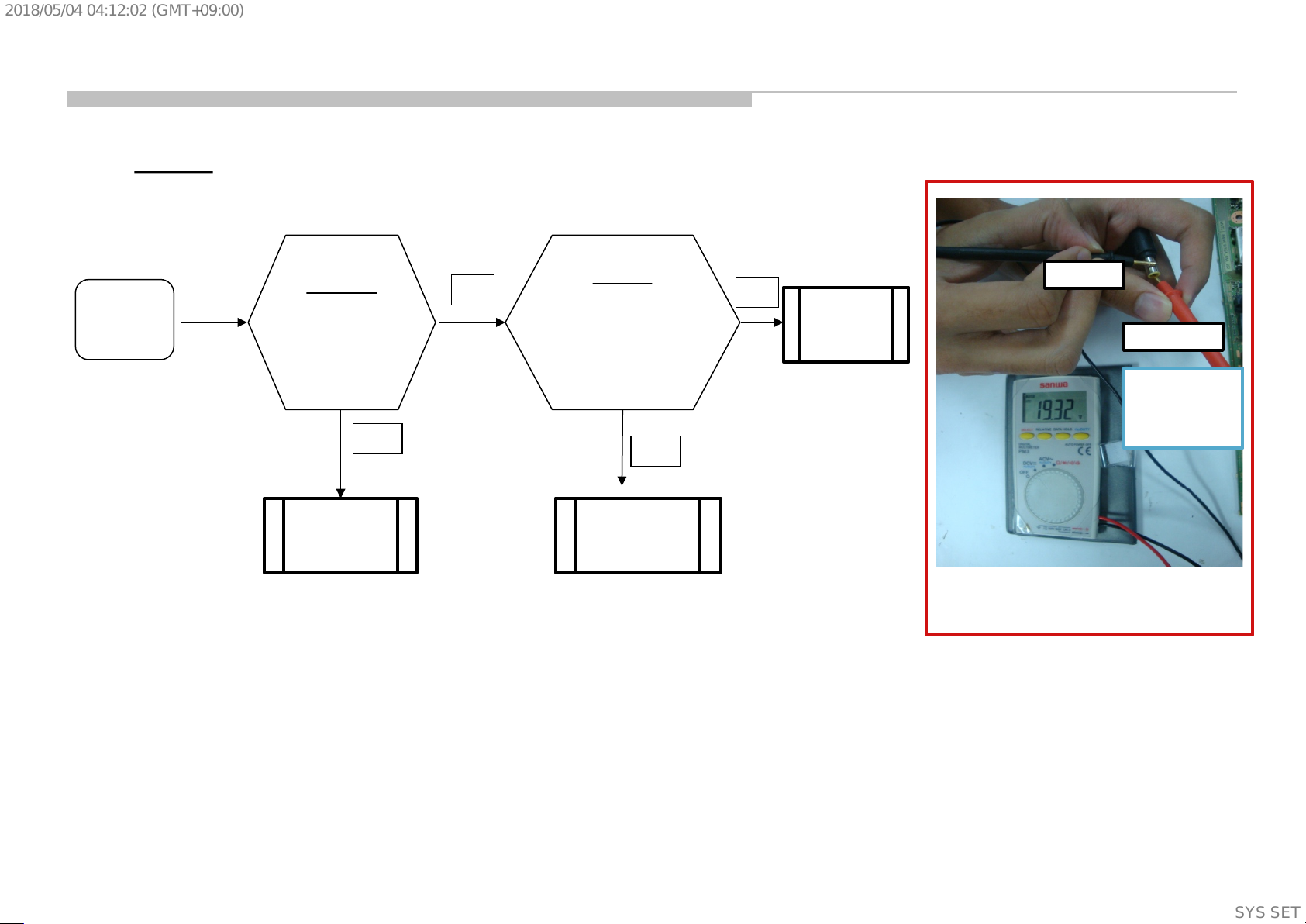
3.12.3 HPD Failure Analysis – HDMI1 and HDMI3
[NG] Any of the part as below
R4021, R4022≠ 4.7KΩ
R4015,R4016, R4018, R4019≠ 1KΩ
HPD
Failure Analysis
Check impedance of
Resistor durin g AC OFF
HDMI1: R4016, R4019 and R4022
HDMI3: R4015, R4018 and R4021
Checking condition:
- TV ON & HDMI Source ON except if the flow men tione d is AC OFF.
- TV HDMI input connected to HDMI source (Player etc.)
- TV Input Selection: HDMI
[OK] All part as below
R4021, R4022 ≈ 4.7KΩ
R4015,R4016, R4018, R4019 ≈ 1KΩ
Check HPD GPIO Line
[OK] Impedance ≈ 100kΩ ±5%
impedance to Ground
during AC OFF
[NG] Impedance ≠ 100kΩ ±5%
HDMI1: R4019*
HDMI3: R4018*
Replace Broken
Resistor and Re-verify
[OK] Picture recovered
END
[NG] No Picture
Internal Main IC (SoC)
Broken (IC5000)
Replace B-Board
and Re-Verify
*Please refer page 67 for actual measuring points
Go to
“I2C Failure Analysis“
Page
(Supplementary
information)
65
SYSSET
Page 66

2018/05/0404:12:02(GMT+09:00)
3.12 HDMI No Picture
3.12.3 HPD Failure Analysis – HDMI2
HPD
Failure Analysis
Check impedance of
Resistor durin g AC OFF
HDMI2: R4043
[NG] Resistance ≠4.7 Ω
Replace Broken
Resistor and Re-verify
[OK] Picture recovered
[OK] Resistance
[NG] No Picture
≈ 4.7 Ω
Checking condition:
- TV ON & HDMI Source ON except if the flow men tione d is AC OFF.
- TV HDMI input connected to HDMI source (Player etc.)
- TV Input Selection: HDMI
Check HPD GPIO Line
impedance to Ground
during AC OFF
HDMI2: R4043*
[NG] Impedance not Open (High Z)
Internal Main IC (SoC)
Broken (IC5000)
Replace B-Board
and Re-Verify
[OK] Impedance ≈ Open (High Z)
Go to
“I2C Failure Analysis“
Page
END
TV Business Division
*Please refer page 67 for actual measuring points
(Supplementary
information)
66
SYSSET
Page 67

2018/05/0404:12:02(GMT+09:00)
3.12 HDMI No Picture
3.12.3 HPD Failure Analysis – Measuring poi nt for H PD GPI O l i ne referenc e s to ground
R4019*
Only meas ure t hi s p o int
reference to GND
HDMI2
R4043*
Only meas ure t hi s p o int
reference to GND
HDMI3
HDMI1
TV Business Division
R4018*
Only meas ure t hi s p o int
referenc e to GND
(Supplementary
information)
67
SYSSET
Page 68

2018/05/0404:12:02(GMT+09:00)
3.12 HDMI No Picture
3.12.4 I2C Fail ure Analy si s
I2C
Failure Analysis
Check impedance of
Resistor during AC OFF
HDMI1: RB4001
HDMI2: RB4002
HDMI3: RB4000
[NG] Impedance
[OK] Picture recovered
≠ 47kΩ
Replace Broken
Resistor and Re-verify
[OK] Impedance
[NG] No Picture
≈ 47kΩ
[NG] HDMI1 Impedance ≠ 140kΩ ±5%
[NG] HDMI2 Impedance not Open (High z)
[NG] HDMI3 Impedance ≠ 140kΩ ±5%
Check I2C GPIO Li ne
impedance to Ground
during AC OFF
HDMI1: CN4001 – Pin15&16
HDMI2: CN4002 – Pin15&16
HDMI3: CN4000 – Pin15&16
Internal Main IC (SoC)
Broken (IC5000)
Replace B-Board
and Re-Verify
Checking condition:
- TV ON & HDMI Source ON except if the flow men tione d is AC OFF.
- TV HDMI input connected to HDMI source (Player etc.)
- TV Input Selection: HDMI
[OK] HDMI1 Impedance ≈ 140kΩ ±5%
[OK] HDMI2 Impedance Open (High Z)
[OK] HDMI3 Impedance ≈ 140kΩ ±5%
Go to
“TMDS Failure Analysis“
Page
END
TV Business Division
68
(Supplementary
information)
68
SYSSET
Page 69

2018/05/0404:12:02(GMT+09:00)
3.12 HDMI No Picture
3.12.5 TMDS Fail ure Anal ysi s
Failure Analysis
Checking condition:
- TV ON & HDMI Source ON except if the flow men tione d is AC OFF.
- TV HDMI input connected to HDMI source (Player etc.)
- TV Input Selection: HDMI
TMDS
Check impedance of Resistor,
CMF (Filter)du r ing AC OFF
HDMI1:RB4007,RB4008,L4002,L4003
HDMI2:RB4003,RB4004,L4004,L4005
HDMI3:RB4005,RB4006,L4000,L4001
[NG] Impedance ≠ 0Ω
Replace Broken
Resistor and Re-verify
[OK] Picture recovered
END
[OK] Impedance ≈ 0±5Ω
[NG] No Picture
Check I2C GPIO Line impedance
to Ground during AC OFF
HDMI1: CN4001 – Pin1,3,4,6,7,9,10,12
HDMI2: CN4002 – Pin1,3,4,6,7,9,10,12
HDMI3: CN4000 – Pin1,3,4,6,7,9,10,12
[NG] Impedance ≠ Open (High-Z)
Internal Main IC (SoC)
Broken (IC5000)
Replace B-Board
and Re-Verify
[OK] Impedance = Open (High-Z)
TV Business Division
69
(Supplementary
information)
69
SYSSET
Page 70

2018/05/0404:12:02(GMT+09:00)
3.12 HDMI No Picture
3.12.6 HDMI Bravia Sync (CEC) Not function
[OK] Source Support CEC &
CEC Source function Normally
Bravia Sync (CEC)
Not Function
Confirm Source (Play er)
CEC Condition/Capability
[NG] Source Not Support CEC /
CEC Source not function Normally
[NG] CEC not functioning
Checking condition:
- TV ON & HDMI Source ON except if the flow men tione d is AC OFF.
- TV HDMI input connected to HDMI source (Player etc.)
- TV Input Selection: HDMI
Change to CEC
Compatible source
[OK] CEC functioning
(CEC) TV setting
[OK] CEC Setting On
Factory Reset &
Change Proven OK
[NG] CEC not functioning
appearance Check On
HDMI connector
[OK] Connector no abnormality
Check impedance
Of R4015 Resistor
during AC OFF
[OK] R4031 ≈ 100Ω ±5%
Bravia Sync
HDMI cable
Physical
[NG] CEC setting Off
[NG] CEC not functioning
[OK] CEC functioning
[NG] Connector abnormal
[NG] CEC not functioning
[NG] R4031 ≠ 100Ω
[NG] CEC not functioning
Turn TV Bravia Sync
HDMI Connector Broken.
Replace & Re-verify
Resistor Broken .
Replace & Re-verify
Replace B-Board
And Re-verify
[OK] CEC functioning
[OK] CEC functioning
[OK] CEC functioning
END
TV Business Division
70
(Supplementary
information)
70
SYSSET
Page 71

2018/05/0404:12:02(GMT+09:00)
3.12 HDMI No Picture
HDMI No picture– Checking Poi nt
R4022
R4019
R4016
VR4010
Zoom 1 :
HDMI1
Pin 19
R4025
L4003
Zoom 4
RB4001
L4002
Pin 1
CN4001
Zoom 1
R4007
R4004
Zoom 2
Zoom 3
R4005
L4005
RB4002
R4044
R4008
L4004
Pin 1
R4043
Zoom 2 :
HDMI2
CN4002
VR4011
Pin 19
TV Business Division
More on the next slide…
(Supplementary
information)
71
SYSSET
Page 72

2018/05/0404:12:02(GMT+09:00)
3.12 HDMI No Picture
HDMI No picture-Checking point ( continued)
Zoom 4
R4031
RB4003
Zoom 4
RB4004
Zoom 3
RB4006
RB4005
RB4008
RB4007
R4036
R4003
RB4000
R4006
R4024
R4021
R4018
R4015
L4001
L4000
Pin 1
Zoom 3 :
HDMI3
VR4009
CN4000
Pin 19
TV Business Division
(Supplementary
information)
72
SYSSET
Page 73

2018/05/0404:12:02(GMT+09:00)
3.12 HDMI No Picture
HDMI No picture– Part List
No Ref No Part No Description
L4000,L4001, L4002, L4003, L4004, L4005 1-460-795-11 COMMON MODE CHOKE COIL
1
RB4003, RB4004, RB4005, RB4006, RB4007,
2
RB4008
1-257-559-21 CONDUCTOR, NETWORK (1005X4)
3
4
5
6
7
8
9
10
11
RB4000, RB4001, RB4002 1-257-548-21 RES, NETWORK 47K (1005X4)
R4043 1-220-803-81 RES, CHIP 4.7 (1005)
R4044 1-218-933-81 RES, CHIP 22 (1005)
R4003, R4004, R4005, R4006, R4007, R4008,
R4031
1-218-941-81 RE S, CHIP 100 (1005)
R4036 1-218-944-81 RE S, CHIP 180 (1005)
R4015,R4016 1-218-953-81 RES, CHIP 1.0K (1005)
R4018,R4019, R4024, R4025 1-250-495-11 RES,METAL FILM CHIP 1.0K(1005)
R4021, R4022 1-218-961-81 RES, CHIP 4.7K (1005)
VR4009, VR4010, VR4011 1-811-656-11 SURGE ABSORBER
TV Business Division
(Supplementary
information)
73
SYSSET
Page 74

2018/05/0404:12:02(GMT+09:00)
3.13 W IFI
3.13 WIFI – Cannot searc h device / Connec tion Fail ed – Gener al C hecki ng
Start
Connection Failed
Check Built-In WiFi
UI
OK
Check WiFi Direct
UI
OK
Check STBY_5V
IC6016
OK
Check Harness
Connection
CN9500
OK
Check TP-VCC
DNUR-SY3
NG: Built-In WiFi Off
NG: WiFi Direct Off
NG: DC Voltage not 5V
NG: Harne ss
Connection Not Ok
NG: DC Voltage is
not 5V
WiFi Feature is
Not Enable
WiFi Direct Feature is
Not Enable
DDCON IC6016
Broken
(Change B*Board)
Harness not in
Good Condition
(Change Harness)
WiFi Module
DNUR-SY3 Broken
(Change WiFi Module)
Check AP/Device
OK
Change B*Board /
WiFi Module
OK
END
Connection Success
NG: Signal Strength
Low
AP Device
Problem
(Change AP/Device)
OK
TV Business Division
(Supplementary
information)
74
SYSSET
Page 75

2018/05/0404:12:02(GMT+09:00)
3.13 W IFI
3.13 WIFI – Cannot searc h device / Connec tion Fail ed – Checking Point
Board Name Board PWB (A si de) Detail
BB9 (IC6016)
IC6016
IC6016
75
SYSSET
75
Page 76

2018/05/0404:12:02(GMT+09:00)
3.13 W IFI
3.13 WIFI – Cannot searc h device / Connec tion Fail ed – Checking Point
76
SYSSET
Page 77
2018/05/0404:12:02(GMT+09:00)
3.14.1 Video Analog Si gnal Path – No Picture – WW Destination
3.14.1 Video Analog Signal Path – No Picture – Gen eral C hecki ng - WW Destination (BB9)
Video
No Picture
Check if input on OSD
is GREY OUT?
(not selectable)
No
Check waveform
before C2006.
Is it Vpp : 1V?
Yes
IC5000 Problem.
(Refer IC troubleshooting
manual)
No
Yes
Check all parts
at CVBS0P signal path.
[VR2000,R2004,
C2000, R2017]
No
Parts Broken.
(Change Part)
Check R2021 voltage.
Is it 3.3V?
No
Yes
J2002 Connector
Problem.
(Change connector)
Yes
J2002 Connectivi ty
Problem.
77
SYSSET
77
Page 78

2018/05/0404:12:02(GMT+09:00)
3.14.1 Video Analog Si gnal Path – No Picture – WW Destination
3.14.1 Video Analog Signal Path – No Picture – Checking Point - WW Destination (BB9)
Board Name Board PWB (A si d e) Details
BB9 (WW)
J2002
VR2000
R2021
R2004
C2000
Details
BB9 (WW)
C2006
R2017
J2002
Details
R2021
VR2000
R2004
C2000
C2006
R2017
TV Business Division
(Supplementary
information)
78
SYSSET
Page 79

2018/05/0404:12:02(GMT+09:00)
3.14.2 Video Analog Signal Path – No Pi cture – UC Destination
3.14.2 Video Analog Signal Path – No Picture – Gen eral C hecki ng - No Picture UC Destination (BB9)
CHL UC
Video
No Picture
Check waveform
before C2006?
Is it Vpp : 1V?
Yes
Check all parts
at CVBS0P signal path.
[VR2000,R2004,
C2000, R2017]
No
No
No Picture or
Abnormal Pictu re
Reinsert Mini Plug
Video Adaptor
until hear
“click” sound
IC5000 Problem
(Refer IC
troubleshooting
manual)
Parts Broken.
(Change Part)
1) Y : 1V
Mini Plug Video Adaptor
Component
No Picture
Check Vpp waveform
at 1) C2003 for Y : 1V?
2) C2008 for Pb :0.7V?
3) C2009 for Pr :0.7V?
Yes
Check all parts.
Y: VR2000,R20 0 4, C2000,
R2014
PB: VR2001, R2005, C2001, R2018
PR: VR2002, R2006, C2002,
R2019
2) Pb : 0.7V
No
No
IC5000 Problem
(Refer IC
troubleshooting
manual)
3) Pr : 0.7V
Parts Broken.
(Change Part)
J2000 connector
Problem.
(Change connector)
TV Business Division
J2000 connector
Problem.
(Change connector)
(Supplementary
information)
79
SYSSET
Page 80

2018/05/0404:12:02(GMT+09:00)
3.14.2 Video Analog Signal Path – No Pi cture – UC Destination
3.14.2 Video Analog Signal Path – No Picture – Checking Point - No Picture UC Destination (BB9)
Board Name Board PWB (A si d e) Details
BB9 (UC)
J2000
R2004
R2005
R2006
C2000
C2001
C2002
VR2000
VR2001
VR2002
BB9 (UC)
C2003
C2006
C2008
C2009
R2014
R2017
R2018
R2019
This image cannot currently be displayed.
This image cannot currently be displayed.
Details
J2000
Details
This image cannot currently be displayed.
VR2002
VR2001
This image cannot currently be displayed.
C2008
C2003
R2014
VR2000
R2018
C2001
R2019
C2002
C2000
R2004
R2006
R2005
C2009
C2006
R2017
TV Business Division
(Supplementary
information)
80
SYSSET
Page 81

2018/05/0404:12:02(GMT+09:00)
3.15 No Power DDCON /LDO
Reference Points
IC Ref Voltage Supply Fuse Enable Output Input
IC6009 5V_DDC_OUT F6004 R6074 C6072 C6066
5V_Main - Q6006(pin2) Q6007(pin1) Q6007(pin3)
IC6010 3.3V_DDC_OUT & STBY F6005 R6089 C6093 C6086
3.3V_Main - Q6008(pin2) Q6009(pin1) Q6009(pin3)
IC6007 1.8V_TU - R6162 C6058 C6055
DDCON
IC6017 1.0V_M3 F6006 R6114 C6146 C6106
IC6004 1.5V_DDR - C6153 C6042 C6040
IC6014 1.05V_M3_A - R6120 C6134 C6130
IC6016 5V_WIFI - R6167 C6141 C6136
IC6018 1.8V_EMMC - IC Pin3 C6125 C6124
LDO
IC6005 1.05V_STBY - IC Pin3 C6050 C6049
TV Business Division
(Supplementary
information)
81
SYSSET
Page 82

2018/05/0404:12:02(GMT+09:00)
Block Diagram
43”
49”
B Board Adaptor /PSU
1.05V LDO
55”
65”
LD
G-Board
19.5V
12.7V
3.3V
DDC
1.0V
DDC
5.0V
DDC
1.5V DDC
1.05V DDC
5V DDC
(WIFI)
1.8V LDO
1.8V DDC
(TUNER)
TV Business Division
(Supplementary
information)
82
SYSSET
Page 83

2018/05/0404:12:02(GMT+09:00)
3.15 No Power DDCON /LDO
DC-DC Converter Overall Check
START
Check C6093 Voltage.
Is the vol ta ge 3.3V?
yes
Check C6042 Voltage.
Is the vol ta ge 1.5V?
yes
Check C6072 Voltage.
Is the vol ta ge 5V?
yes
Check C6141 Voltage.
Is the vol ta ge 5V?
no
no
no
no
DDC: +3.3V_DDC_OUT check
DDC: +1.5V_DDR check
DDC: +5.0V_DDC_OUT check
DDC: +5V_WIFI check
Check C6146 Voltage.
Is the vol ta ge 1V?
yes
Check C6134,
C6050 is it
1.05V?
yes
Check C6058 is
it 1.8V?
yes
Check C6125 is
it 1.8V?
yes
Check 3.3V_MAIN
C6130 Voltage.
Is the vol ta ge 3.3V?
no
no
no
no
no
DDC: +1.0V_M3 check
LDO: +1.05V_M3_xx check
DDC: +1.8V_TU check
DDC: +1.8V_EMMC check
SW: +3.3V_MAIN check
yes
TV Business Division
yes
END (DDCON/LDO working normal)
(Supplementary
information)
83
SYSSET
Page 84

2018/05/0404:12:02(GMT+09:00)
3.15 No Power DDCON /LDO
DDC: +3.3V_DDC_OUT check
START
LD-Board model
Check input
F6005 voltage
Is voltage >1 9 . 0 V?
yes
Check fu se
F6005
Is fuse OK?
yes
yes
no
Check EN signa l
R6088 voltage
Is voltage >2 .9V?
yes
Check Vcc
C6082 voltage
Is voltage >5 .3V?
Is voltage >1 2 . 0 V?
yes
no
Change F6005
G-Board model
Check input
F6005 voltage
no
no
G-Board/LD-Board
no
Change IC 6010
TV Business Division
END
yes
CHL 55”/65”= G-Board model (PSU)
CHL43”/49”=LD-Board model (ADP)
(Supplementary
information)
84
SYSSET
Page 85

2018/05/0404:12:02(GMT+09:00)
3.15 No Power DDCON /LDO
DDC: +1.5V_DDR check
START
no
Check IC6009 Vcc voltage
C6066
Is voltage >19.5V?
yes
Check Vcc voltage
C6040
Is voltage >=5V?
yes
Is IC6004 mounted?
yes
Check Enable
IC6019 #pin1
Is voltage >2.5V?
yes
no
no
no
Check Vcc voltage
C6040
Is voltage >3.3V?
yes
Check
D6002
Is diode ok?
yes
Change IC6019
no
no
Check
D6001
Is diode ok?
no
yes
Change D6002
Check +5V_MAIN DDCON (IC6009)
Change D6001
Check +3.3V_STBY.
G board or IC6010
Change DDCON
IC6004
TV Business Division
(Supplementary
information)
85
SYSSET
Page 86

2018/05/0404:12:02(GMT+09:00)
3.15 No Power DDCON /LDO
SW: +5V_MAIN check
START
Check VG signa l
Q6007 #pin 1
Is voltage > 4.9V?
yes
Check VB signal
Q6006 #pin 2
Is voltage > 1.9V?
no
Other Issue
no
yes
Change Q6007
Change Q6006
TV Business Division
86
(Supplementary
information)
86
SYSSET
Page 87

2018/05/0404:12:02(GMT+09:00)
3.15 No Power DDCON /LDO
DDC: +5.0V_DDC_OUT check
START
Check fu se
F6004
Is fuse OK?
LD-Board model G-Board model
Check input
F6004 voltage
Is voltage >1 9 . 0 V?
yes
yes
no
Check input
F6004 voltage
Is voltage >1 2 . 0 V?
no
yes
Check EN signa l
R6073 voltage
Is voltage >2 .5V?
yes
no
yes
Check Vcc
C6062 voltage
Is voltage >5 V?
no
Change F6004
no
G-Board/LD-Board
G-Board/LD-Board
Change IC 6009
TV Business Division
END
yes
CHL 55”/65”= G-Board model (PSU)
CHL 43”/49”= L D -Board model (ADP)
87
(Supplementary
information)
87
SYSSET
Page 88

2018/05/0404:12:02(GMT+09:00)
3.15 No Power DDCON /LDO DDC: +1.0V_M3 check
START
Check fu se
F6006
Is fuse OK?
LD-Board model G-Board model
Check input
F6006 voltage
Is voltage >1 9 . 0 V?
yes
yes
no
Check input
F6006 voltage
Is voltage >1 2 . 0 V?
no
yes
Check EN signa l
R6114 voltage
Is voltage >1 .9V?
yes
no
yes
Check Vcc
C6102 voltage
Is voltage >5 .3V?
no
yes
Change F6006
no
G-Board/LD-Board
MTK IC damag e
Change IC 6017
END
TV Business Division
CHL 55”/65”= G-Board model (PSU)
CHL43”/49”=LD-Board model (ADP)
88
(Supplementary
information)
88
SYSSET
Page 89

2018/05/0404:12:02(GMT+09:00)
3.15 No Power DDCON /LDO
LDO: +1.05V_M 3_STBY
+1.05V_M3_STBY
START
yes
Check input
C6049 voltage
Is voltage >3.0V?
yes
Check EN signal
IC6005 #pin3
Is voltage >3.0V?
yes
no
no
DDC: 3.3V_DDC_OUT check
DDC: 3.3V_DDC_OUT check
LDO: +1.8V_EM M C
+1.8V_EMMC
START
yes
Check input
C6124 voltage
Is voltage >3.0V?
yes
Check EN signal
IC6018 #pin3
Is voltage >3.0V?
yes
no
DDC: 3.3V Switching check
no
DDC:3.3V Switching check
Change IC6005
TV Business Division
Change IC6018
89
(Supplementary
information)
89
SYSSET
Page 90

2018/05/0404:12:02(GMT+09:00)
3.15 No Power DDCON /LDO
DDC: + 1.8V_TU chec k
START
Check voltage
C6055
Is voltage >5.0V?
yes
Check EN si gnal
R6162
Is voltage >1.6V?
yes
Change IC6007
no
no
Check
D6011
Is diode ok?
yes
Check
D6009
Is diode ok?
yes
no
no
Change D6011
Check +5.0V_DD C _OU T
Change D6009
MTK IC damage
TV Business Division
90
(Supplementary
information)
90
SYSSET
Page 91

2018/05/0404:12:02(GMT+09:00)
3.15 No Power DDCON /LDO
DDC: 1.05V_M3_A check
START
Check voltage
C6130
Is voltage >3.0V?
yes
Check EN si gnal
R6120
Is voltage >3.0V?
yes
Change IC6014
no
DDC: 3.3V switchi ng check
no
DDC: 3.3V switchi ng check
TV Business Division
91
(Supplementary
information)
91
SYSSET
Page 92

2018/05/0404:12:02(GMT+09:00)
3.15 No Power DDCON /LDO
DDC: 5.0V_WIFI check
START
Check voltage
C6136
Is voltage >3.0V?
yes
Check EN si gnal
R6167
Is voltage >3.0V?
yes
Change IC6016
no
no
Check +3.3V_STBY.
G board or IC6010
MTK IC damage
TV Business Division
92
(Supplementary
information)
92
SYSSET
Page 93

2018/05/0404:12:02(GMT+09:00)
3.15 No Power DDCON /LDO
SW: +3.3V_MAIN check
START
Check VG signal
Q6009 #pin1
Is voltage > 3.0V?
yes
Check VB signal
Q6008 #pin2
Is voltage > 1.9V?
no
Other Issue
no
Change Q6009
yes
Change Q6008
TV Business Division
93
(Supplementary
information)
93
SYSSET
Page 94

2018/05/0404:12:02(GMT+09:00)
3.15 No Power DDCON /LDO
DDC & LDO Locations
Q6008
Q6009
IC6004
IC6010
IC6009
IC6017
Q6006
Q6007
IC6014
IC6016
IC6018
TV Business Division
IC6005
94
IC6007
(Supplementary
information)
94
SYSSET
Page 95

2018/05/0404:12:02(GMT+09:00)
3.15 No Power DDCON /LDO
DDC & LDO Locations
DDC: +3.3V_DDC_OUT DDC: +1.5V_DDR DDC: +5.0V_DDC_OUT
C6093
F6004
C6066
C6086
IC6010
F6005
C6153
C6040
IC6004
C6042
IC6009
C6072
TV Business Division
95
(Supplementary
information)
95
SYSSET
Page 96

2018/05/0404:12:02(GMT+09:00)
3.15 No Power DDCON /LDO
DDC & LDO Locations
DDC: +5V_WIFI DDC: +1.0V_M3 DDC: +1.8V_TU
C6141
IC6016
C6136
R6167
R6114
C6055
IC6017
R6162
IC6007
F6006
C6058
C6106
C6146
TV Business Division
96
(Supplementary
information)
96
SYSSET
Page 97
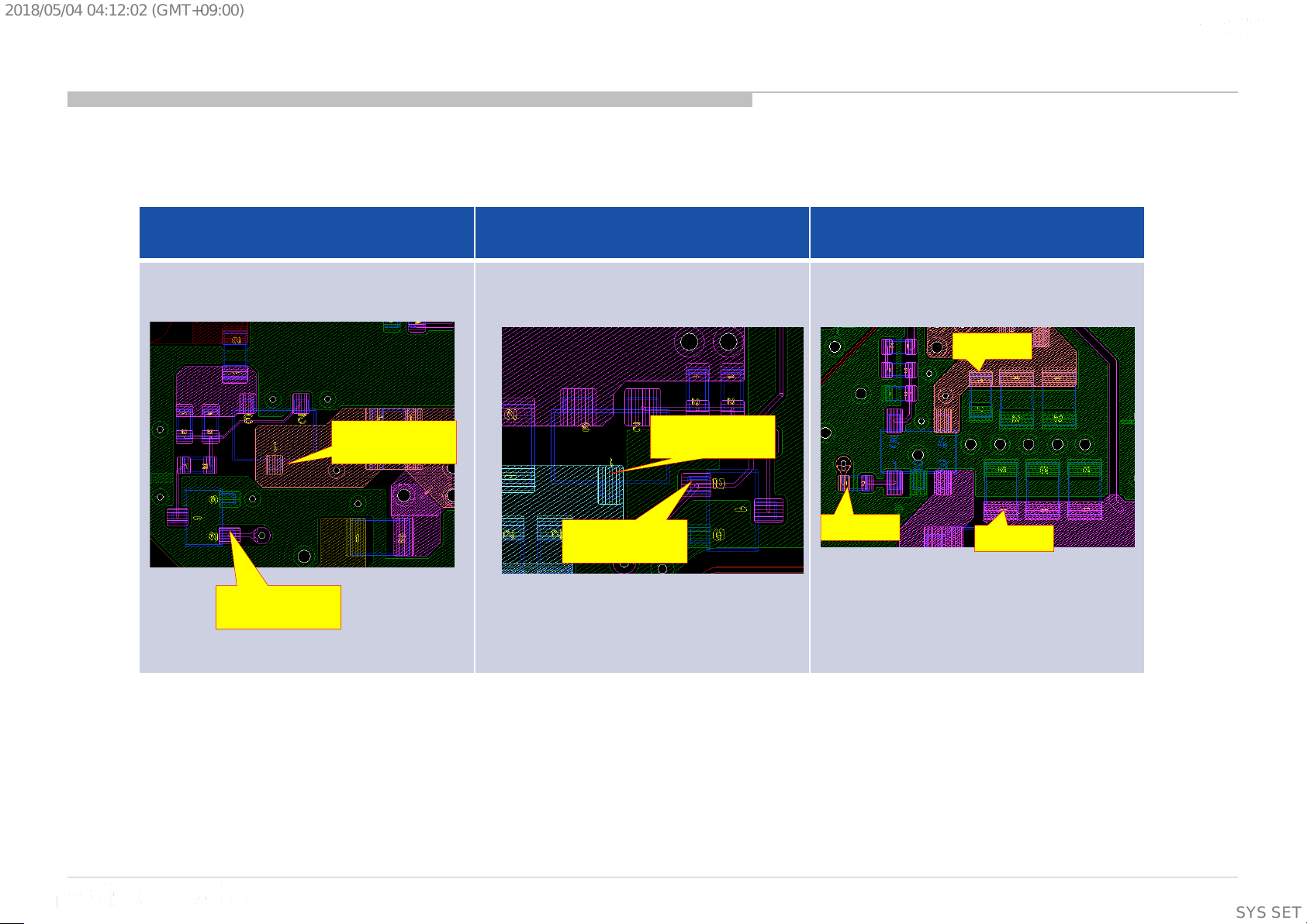
2018/05/0404:12:02(GMT+09:00)
3.15 No Power DDCON /LDO
DDC & LDO Locations
DDC: +3.3V_MAIN DDC: +5V_MAIN DDC: +1.05V_M3_A
C6130
Q6008
#P IN 2 (V B)
Q6009
#P IN 1 (V G)
Q6007
#P IN 1 (V G)
#P IN 2 (V B)
Q6006
R6120
IC6014
C6134
TV Business Division
97
(Supplementary
information)
97
SYSSET
Page 98

2018/05/0404:12:02(GMT+09:00)
3.15 No Power DDCON /LDO
DDC & LDO Locations
DDC: +1.05V_STBY DDC: +1.80V_EMMC
C6050
#PIN3
#PIN3
C6124
C6125
IC6005
IC6018
C6049
TV Business Division
98
(Supplementary
information)
98
SYSSET
Page 99
2018/05/0404:12:02(GMT+09:00)
Troubleshooting manual summary – No Sound
Section
3
Problem/Issue
No Sound
3.16.1 Audio D.Amp IC Normal Operation Condition
3.16.2 Troubleshooting Detail Audio Problem
3.16.2.1 Main Speaker N o Sound
3.16.2.2 Headphone (HP) Out No Sound
3.16.2.3 Analog Audio Input No Sound
3.16.2.4 Analog RF No Sound
3.16.2.5 HDMI Audio No Sound
3.16.2.6 HDMI ARC Failure
3.16.2.7 USB Audio No Sound
3.16.2.7.1 USB Port1 – No Detection / Cannot Play / No Picture / No Sound
3.16.2.7.2 USB Port2 – No Detection / Cannot Play / No Picture / No Sound
Title
TV Business Division
99
(Supplementary
information)
99
SYSSET
Page 100

2018/05/0404:12:02(GMT+09:00)
3.16.1 Audio D Am p IC Normal Operation Condition
3.16.1 Audio D Amp IC Normal Operation Condition
Label Name
AC Adapter PSU board Common
Voltage Voltage Frequency
1 SDI 3.3Vpp 3.3Vpp Clock signal
2 SDO 0V 0V 3 RESETB 3.3V 3.3V 4 LRCK 3.3Vpp 3.3Vpp 48kHz
5 SCLK 3.3Vpp 3.3Vpp 3.07MHz
6 MCLK 0V 0V 7 DVSS 0V 0V 8 VR_DIG 1.8V 1.8V 9 DVDD 3.3V 3.3V -
10 AVSS 0V 0V 11 AVCC 3.3V 3.3V 12 GVDD 5V 5V 13 VR_ANA 5V 5V 14 BSTPR 14.7Vrms 11.4Vrms -
Label Name
AC Adapter PSU board Common
Voltage Voltage Frequency
15 VOUTPR 9.7Vrms 6.4Vrms ~384kHz
16 PVDDR 19.5V 12.7V
17 VOUTNR 9.7Vrms 6.4Vrms ~384kHz
18 BSTNR 14.7Vrms 11.4Vrms 19 BSTNL 14.7Vrms 11.4Vrms -
20 VOUTNL 9.7Vrms 6.4Vrms ~384kHz
21 PVDDL 19.5V 12.7V -
22 VOUTPL 9.7Vrms 6.4Vrms ~384kHz
23 BSTPL 14.7Vrms 11.4Vrms 24 PWDNN 3.3V 3.3V 25 FAULTB 3.3V 3.3V 26 A_SEL 0V 0V 27 SDA 3.3Vpp 3.3Vpp Clock signal
28 SCL 3.3Vpp 3.3Vpp Clock signal
TV Business Division
100
(Supplementary
information)
100
SYSSET
 Loading...