

Sony ICX422AL Datasheet
ICX422AL
Diagonal 11mm (Type 2/3) CCD Image Sensor for EIA B/W Video Cameras
Description
The ICX422AL is an interline CCD solid-state image
sensor suitable for EIA B/W video cameras with a
diagonal 11mm (Type 2/3) system. Compared with the
current product ICX082AL, basic characteristics such
as sensitivity and smear are improved drastically and
high saturation characteristics are realized.
This chip features a field period readout system and
an electronic shutter with variable charge-storage
time. This chip is compatible with the pins of the
ICX082AL and has the same drive conditions.
Features
• High sensitivity (+3.0dB compared with the ICX082AL)
• Low smear (–10.0dB compared with the ICX082AL)
• High saturation signal (+2.0dB compared with the ICX082AL)
• High resolution and Low dark current
• Excellent antiblooming characteristics
• Continuous variable-speed shutter
Device Structure
• Interline CCD image sensor
• Optical size: Diagonal 11mm (Type 2/3)
• Number of effective pixels: 768 (H) × 494 (V) approx. 380K pixels
• Total number of pixels: 811 (H) × 508 (V) approx. 410K pixels
• Chip size: 10.25mm (H) × 8.5mm (V)
• Unit cell size: 11.6µm (H) × 13.5µm (V)
• Optical black: Horizontal (H) direction: Front 3 pixels, rear 40 pixels
Vertical (V) direction: Front 12 pixels, rear 2 pixels
• Number of dummy bits: Horizontal 22
Vertical 1 (even fields only)
• Substrate material: Silicon
20 pin DIP (Ceramic)
V
3
Pin 11
Optical black position
H
(T op View)
Pin 1
40
2
12
Sony reserves the right to change products and specifications without prior notice. This information does not convey any license by
any implication or otherwise under any patents or other right. Application circuits shown, if any, are typical examples illustrating the
operation of the devices. Sony cannot assume responsibility for any problems arising out of the use of these circuits.
– 1 –
E01X22-PS
Block Diagram and Pin Configuration
(Top view)
V
L
7
GND
9
DD
V
10
V
OUT
11
V
GG
V
SS
GND
12
13
14
Output Unit
15 16 17 18 19 20
RG Hφ
RD Hφ
V
L
Vertical Register
Horizontal Register
1
2
HIS
Note)
ICX422AL
Vφ
4
1
Vφ
3
2
3
Vφ
2
4
SUB
GND
5
Vφ
1
6
Note) : Photo sensor
Pin Description
Pin No. Symbol Description
1
2
3
4
5
6
7
8
9
10
Vφ4
Vφ3
Vφ2
SUB
GND
Vφ1
VL
NC
GND
VDD
Vertical register transfer clock
Vertical register transfer clock
Vertical register transfer clock
Substrate (overflow drain)
GND
Vertical register transfer clock
Protective transistor bias
GND
Output amplifier drain power
Description
Pin No. Symbol
11
12
13
14
15
16
17
18
19
20
VOUT
VGG
VSS
GND
RD
RG
VL
Hφ1
Hφ2
HIS
Signal output
Output amplifier gate bias
Output amplifier source
GND
Reset drain
Reset gate clock
Protective transistor bias
Horizontal register transfer clock
Horizontal register transfer clock
Horizontal register input source bias
– 2 –
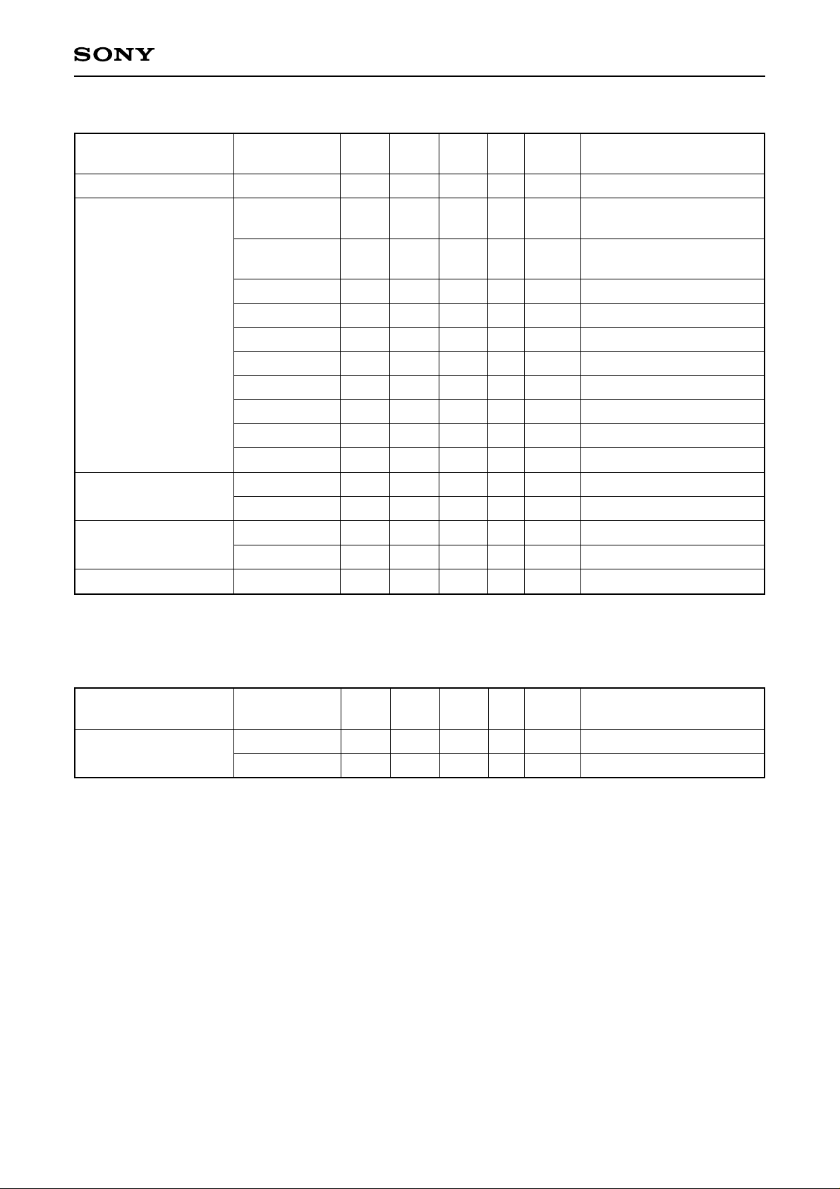
Absolute Maximum Ratings
ICX422AL
Item
Substrate voltage SUB – GND
HIS, VDD, RD, VOUT, VSS – GND
Supply voltage
HIS, VDD, RD, VOUT, VSS – SUB
Vertical clock input
voltage
Vertical clock input pins – GND
Vertical clock input pins – SUB
Voltage difference between vertical clock input pins
Voltage difference between horizontal clock input pins
Hφ1, Hφ2 – Vφ4
Hφ1, Hφ2, RG, VGG – GND
Hφ1, Hφ2, RG, VGG – SUB
VL – SUB
Vφ1, Vφ3, HIS, VDD, RD, VOUT – VL
RG – VL
Vφ2, Vφ4, VGG, VSS, Hφ1, H φ2 – VL
Storage temperature
Operating temperature
Ratings
–0.3 to +55
–0.3 to +20
–55 to +10
–15 to +20
to +10
to +15
to +17
–17 to +17
–10 to +15
–55 to +10
–65 to +0.3
–0.3 to +30
–0.3 to +24
–0.3 to +20
–30 to +80
–10 to +60
Unit Remarks
V
V
V
V
V
1
V
∗
V
V
V
V
V
V
V
V
°C
°C
1
∗
27V (Max.) when clock width < 10µs, clock duty factor < 0.1%.
Bias Conditions
Item
Output amplifier drain voltage
Reset drain voltage
Output amplifier gate voltage
Output amplifier source
Substrate voltage adjustment range
Substrate voltage adjustment precision
Reset gate clock voltage adjustment range
Reset gate clock voltage adjustment precision
Protective transistor bias
Horizontal register input source bias
Symbol
VDD
VRD
VGG
VSS
VSUB
∆VSUB
VRGL
∆VRGL
VL
VHIS
Min.
14.7
14.7
3.8
15.0
15.0
4.2
15.3
15.3
4.6
Ground with 750Ω resistor
9
–3
0
–3
–11
14.7
–10.5
15.0
19
+3
3.0
+3
–10
15.3
Unit
V
V
V
V
%
V
%
V
V
RemarksTyp. Max.
VRD = VDD
±5%
2
∗
2
∗
3
∗
VHIS = VDD
– 3 –
DC Characteristics
ICX422AL
Item
Output amplifier drain current
Input current
Input current
2
∗
Indications of substrate voltage (VSUB) and reset gate clock voltage (VRGL) setting value
Symbol6Min. Unit RemarksTyp. Max.
IDD
IIN1
IIN2
1
10
mA
µA
µA
4
∗
5
∗
The setting value of the substrate voltage and reset gate clock voltage are indicated on the back of the
image sensor by a special code. Adjust the substrate voltage (VSUB) and reset gate clock voltage (VRGL) to
the indicated voltage. The adjustment precision is ±3%.
VSUB code — one character indication
VRGL code — one character indication ↑↑
VRGL code VSUB code
"Code" and optimal setting correspond to each other as follows.
VRGL code
Optimal setting1020.531.041.552.062.573.0
VSUB code
Optimal settingD9.0
E
9.5f10.0G10.5h11.0J11.5K12.0L12.5m13.0N13.5P14.0Q14.5R15.0S15.5T16.0U16.5V17.0W17.5X18.0Y18.5Z19.0
<Example> "5K" → VRGL = 2.0V
VSUB = 12.0V
3
∗
This must no exceed the VVL voltage of the vertical clock waveform.
4
∗
1) Current to each pin when 20V is applied to VDD, RD, VOUT, VSS, HIS and SUB pins, while pins that are
not tested are grounded.
2) Current to each pin when 20V is applied sequentially to V φ1, Vφ2, Vφ3 and Vφ4 pins, while pins that are
not tested are grounded. However, 20V is applied to SUB pin.
3) Current to each pin when 15V is applied sequentially to Hφ1, Hφ2, RG and VGG pins, while pins that are
not tested are grounded. However, 15V is applied to SUB pin.
4) Current to VL pin when 30V is applied to Vφ1, Vφ3, HIS, VDD, RD and VOUT pins or when, 24V is applied
to RG pin or when, 20V is applied to Vφ2, Vφ4, VGG, VSS, Hφ1 and Hφ2 pins, while VL pin is grounded.
However, GND and SUB pins are left open.
5
∗
Current to SUB pin when 55V is applied to SUB pin, while pins that are not tested are grounded.
– 4 –
Clock V olta ge Conditions
ICX422AL
Item
Readout clock voltage
Vertical transfer clock
voltage
Horizontal transfer
clock voltage
Reset gata clock
voltage
Symbol
VVT
VVH1, VVH2,
VVH3, VVH4
VVL1, VVL2,
VL3, VVL4
V
VφV
| VVH1 – VVH2 |
VVH3 – VVH
VVH4 – VVH
VVHH
VVHL
VVLH
VVLL
VφH
VHL
VφRG
VRGL
Min.
14.5
–0.6
8.9
–0.5
–0.5
6.0
–3.5
6.0
0
Typ.
15.0
–9.6
Max. Unit
15.5
V
0
V
V
V
0.2
0.8
1.0
0.8
0.8
8.0
–3.0
13.0
3.0
V
0
V
0
V
V
V
V
V
V
V
V
V
Waveform
diagram
1
2
2
2
2
2
2
2
2
2
2
3
3
3
3
Remarks
VVH = (VVH1 + VVH2)/2
VVL = (VVL3 + VVL4)/2
VφV = VVHn – VVLn (n = 1 to 4)
High-level coupling
High-level coupling
Low-level coupling
Low-level coupling
1
∗
Substrate clock voltage
1
∗
The reset gate clock voltage need not be adjusted when the reset gate clock is driven when the
VφSUB
27.0
32.0
V
4
specifications are as given below. In this case, the reset gate clock voltage setting indicated on the back of
the image sensor has not significance.
V
V
Waveform
diagram
3
3
Remarks
Item
Reset gate clock
voltage
VRGL
VφRG
Symbol
Min.
–0.2
8.5
Typ.
0
9.0
Max. Unit
0.2
9.5
– 5 –
 Loading...