

Sony ICX418ALB User Manual
ICX418ALB
Diagonal 8mm (Type 1/2) CCD Image Sensor for EIA B/W Video Cameras
Description
The ICX418ALB is an interline CCD solid-state
image sensor suitable for EIA B/W video cameras
with a diagonal 8mm (Type 1/2) system. Compared
with the current product ICX038DLB, basic
characteristics such as sensitivity, smear, dynamic
range and S/N are improved drastically.
This chip features a field period readout system and
an electronic shutter with variable charge-storage
time. Also, this outline is miniaturized by using
original package. This chip is compatible with the
pins of the ICX038DLB and has the same drive
conditions.
Features
• High sensitivity (+5.0dB compared with the ICX038DLB)
• Low smear (–5.0dB compared with the ICX038DLB
• High D range (+2.0dB compared with the ICX038DLB)
• High S/N
• High resolution and low dark current
• Excellent antiblooming characteristics
• Continuous variable-speed shutter
• Substrate bias: Adjustment free (external adjustment also possible with 6 to 14V)
• Reset gate pulse: 5Vp-p adjustment free (drive also possible with 0 to 9V)
• Horizontal register: 5V drive
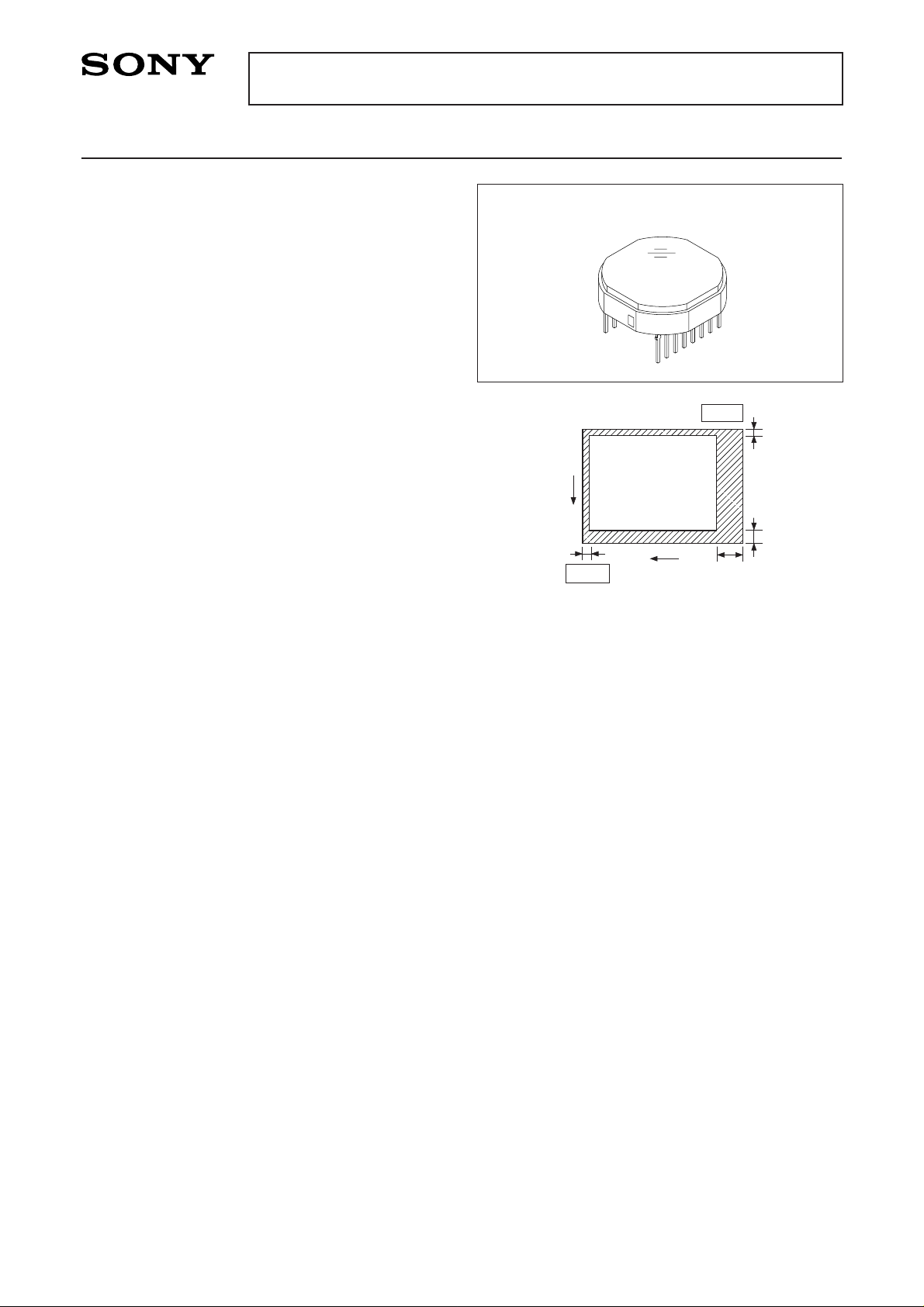
• Maximum package dimensions: φ13.2mm
16 pin DIP (Ceramic)
V
3
Pin 9
Optical black position
H
(T op View)
Pin 1
2
12
40
Device Structure
• Interline CCD image sensor
• Optical size: Diagonal 8mm (Type 1/2)
• Number of effective pixels: 768 (H) × 494 (V) approx. 380K pixels
• Total number of pixels: 811 (H) × 508 (V) approx. 410K pixels
• Chip size: 7.40mm (H) × 5.95mm (V)
• Unit cell size: 8.4µm (H) × 9.8µm (V)
• Optical black: Horizontal (H) direction: Front 3 pixels, rear 40 pixels
Vertical (V) direction: Front 12 pixels, rear 2 pixels
• Number of dummy bits: Horizontal 22
Vertical 1 (even fields only)
• Substrate material: Silicon
Sony reserves the right to change products and specifications without prior notice. This information does not convey any license by
any implication or otherwise under any patents or other right. Application circuits shown, if any, are typical examples illustrating the
operation of the devices. Sony cannot assume responsibility for any problems arising out of the use of these circuits.
– 1 –
E01908A41

ICX418ALB
USE RESTRICTION NOTICE (December 1, 2003 ver.)
This USE RESTRICTION NOTICE ("Notice") is for customers who are considering or currently using the CCD
products ("Products") set forth in this specifications book. Sony Corporation ("Sony") may, at any time, modify
this Notice which will be available to you in the latest specifications book for the Products. You should abide by
the latest version of this Notice. If a Sony subsidiary or distributor has its own use restriction notice on the
Products, such a use restriction notice will additionally apply between you and the subsidiary or distributor. You
should consult a sales representative of the subsidiary or distributor of Sony on such a use restriction notice
when you consider using the Products.
Use Restrictions
• The Products are intended for incorporation into such general electronic equipment as office products,
communication products, measurement products, and home electronics products in accordance with the
terms and conditions set forth in this specifications book and otherwise notified by Sony from time to time.
• You should not use the Products for critical applications which may pose a life- or injury- threatening risk or
are highly likely to cause significant property damage in the event of failure of the Products. You should
consult your Sony sales representative beforehand when you consider using the Products for such critical
applications. In addition, you should not use the Products in weapon or military equipment.
• Sony disclaims and does not assume any liability and damages arising out of misuse, improper use,
modification, use of the Products for the above-mentioned critical applications, weapon and military
equipment, or any deviation from the requirements set forth in this specifications book.
Design for Safety
• Sony is making continuous efforts to further improve the quality and reliability of the Products; however,
failure of a certain percentage of the Products is inevitable. Therefore, you should take sufficient care to
ensure the safe design of your products such as component redundancy, anti-conflagration features, and
features to prevent mis-operation in order to avoid accidents resulting in injury or death, fire or other social
damage as a result of such failure.
Export Control
• If the Products are controlled items under the export control laws or regulations of various countries, approval
may be required for the export of the Products under the said laws or regulations. You should be responsible
for compliance with the said laws or regulations.
No License Implied
• The technical information shown in this specifications book is for your reference purposes only. The
availability of this specifications book shall not be construed as giving any indication that Sony and its
licensors will license any intellectual property rights in such information by any implication or otherwise. Sony
will not assume responsibility for any problems in connection with your use of such information or for any
infringement of third-party rights due to the same. It is therefore your sole legal and financial responsibility to
resolve any such problems and infringement.
Governing Law
• This Notice shall be governed by and construed in accordance with the laws of Japan, without reference to
principles of conflict of laws or choice of laws. All controversies and disputes arising out of or relating to this
Notice shall be submitted to the exclusive jurisdiction of the Tokyo District Court in Japan as the court of first
instance.
Other Applicable Terms and Conditions
• The terms and conditions in the Sony additional specifications, which will be made available to you when you
order the Products, shall also be applicable to your use of the Products as well as to this specifications book.
You should review those terms and conditions when you consider purchasing and/or using the Products.
– 2 –
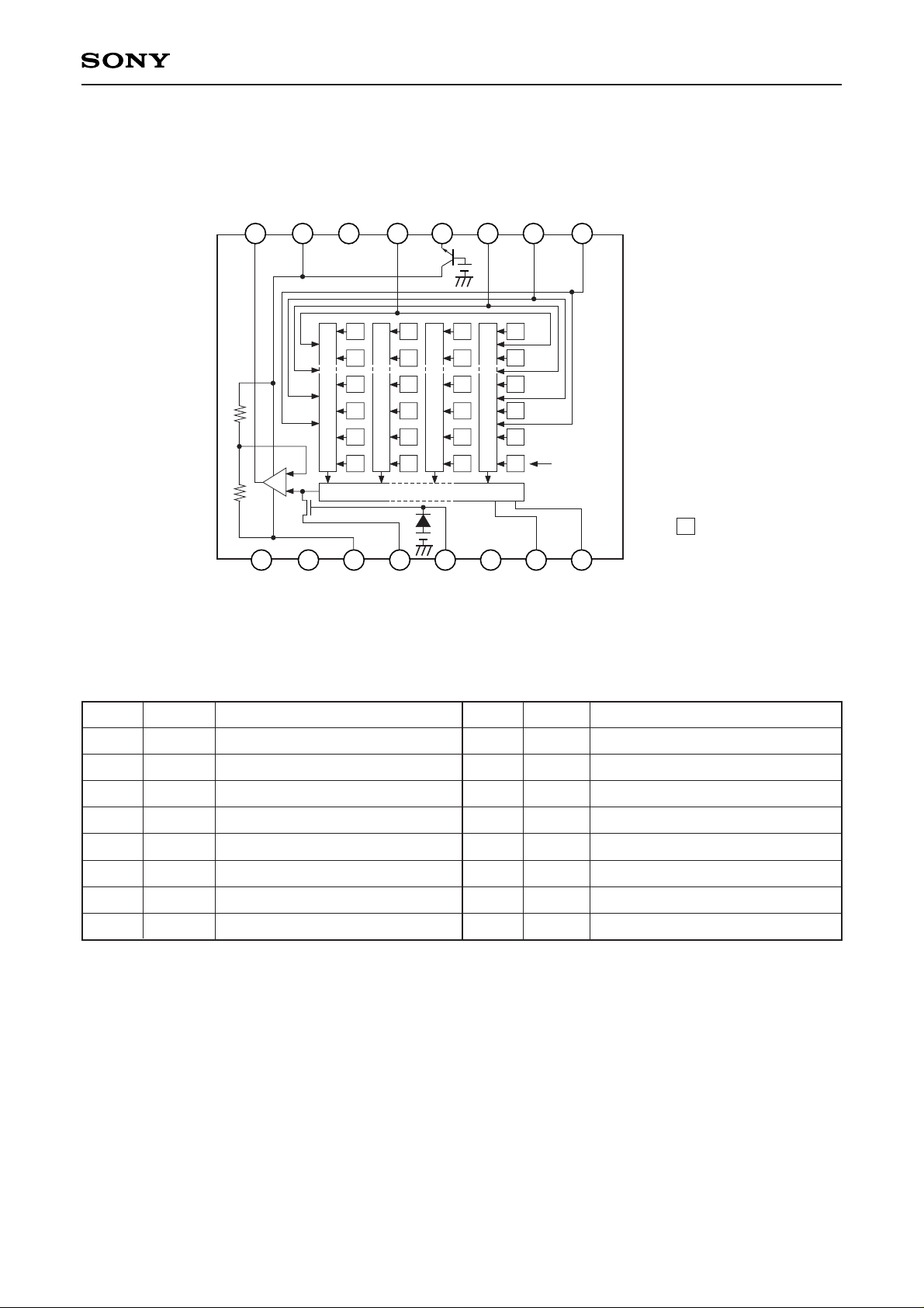
Block Diagram and Pin Configuration
(T op Vie w)
ICX418ALB
OUTVDD
V
8 7 6 5 4 3 2 1
Vertical Register
9 10 11 12 13 14 15 16
NC
NC
1
L
V
Vφ
Horizontal Register
RD
GND
SUB
φ
RG
φ
2
Vφ
DSUB
V
3
Vφ
Note)
1
Hφ
4
Vφ
Note) : Photo sensor
2
Hφ
Pin Description
Pin No. Pin No.
1
2
3
4
5
6
7
8
Symbol Description
Vφ4
Vφ3
Vφ2
φSUB
Vφ1
VL
VDD
VOUT
Vertical register transfer clock
Vertical register transfer clock
Vertical register transfer clock
Substrate clock
Vertical register transfer clock
Protective transistor bias
Output circuit supply voltage
Signal output
9
10
11
12
13
14
15
16
Symbol Description
NC
NC
GND
RD
φRG
VDSUB
Hφ1
Hφ2
GND
Reset drain bias
Reset gate clock
Substrate bias circuit supply voltage
Horizontal register transfer clock
Horizontal register transfer clock
– 3 –
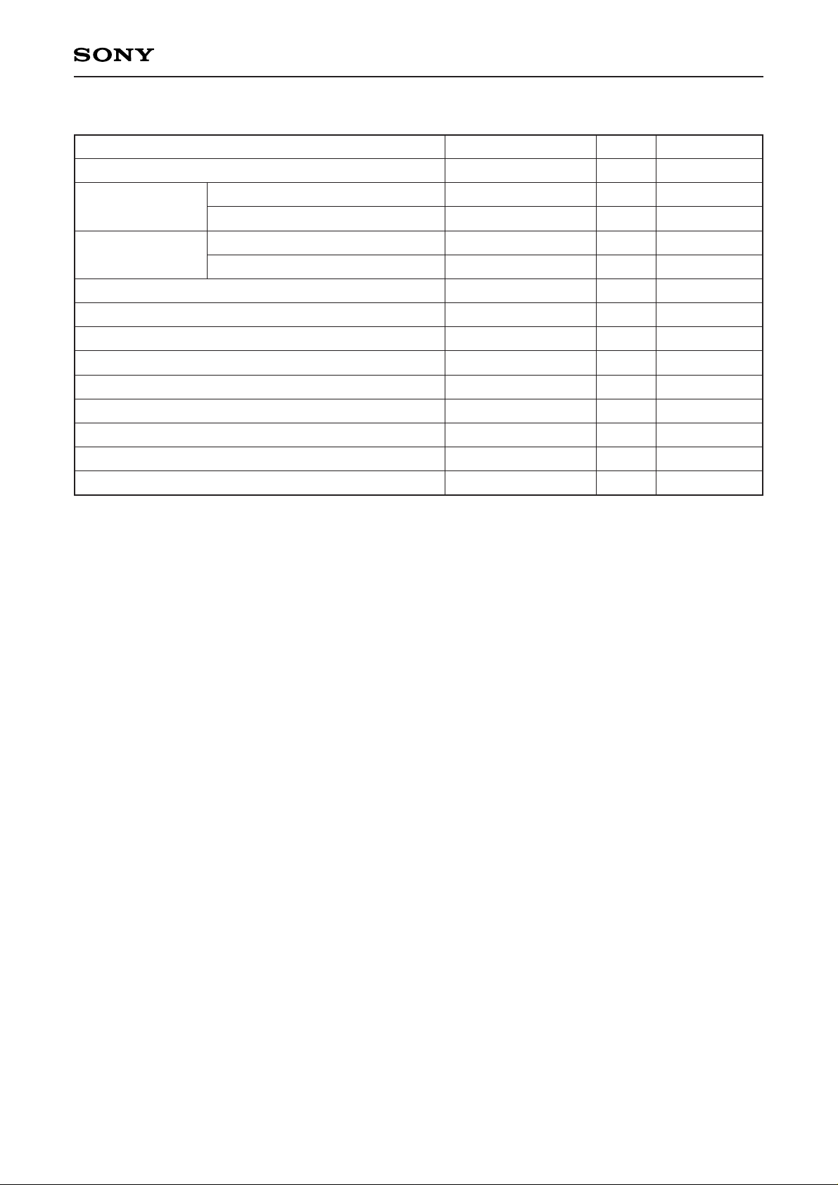
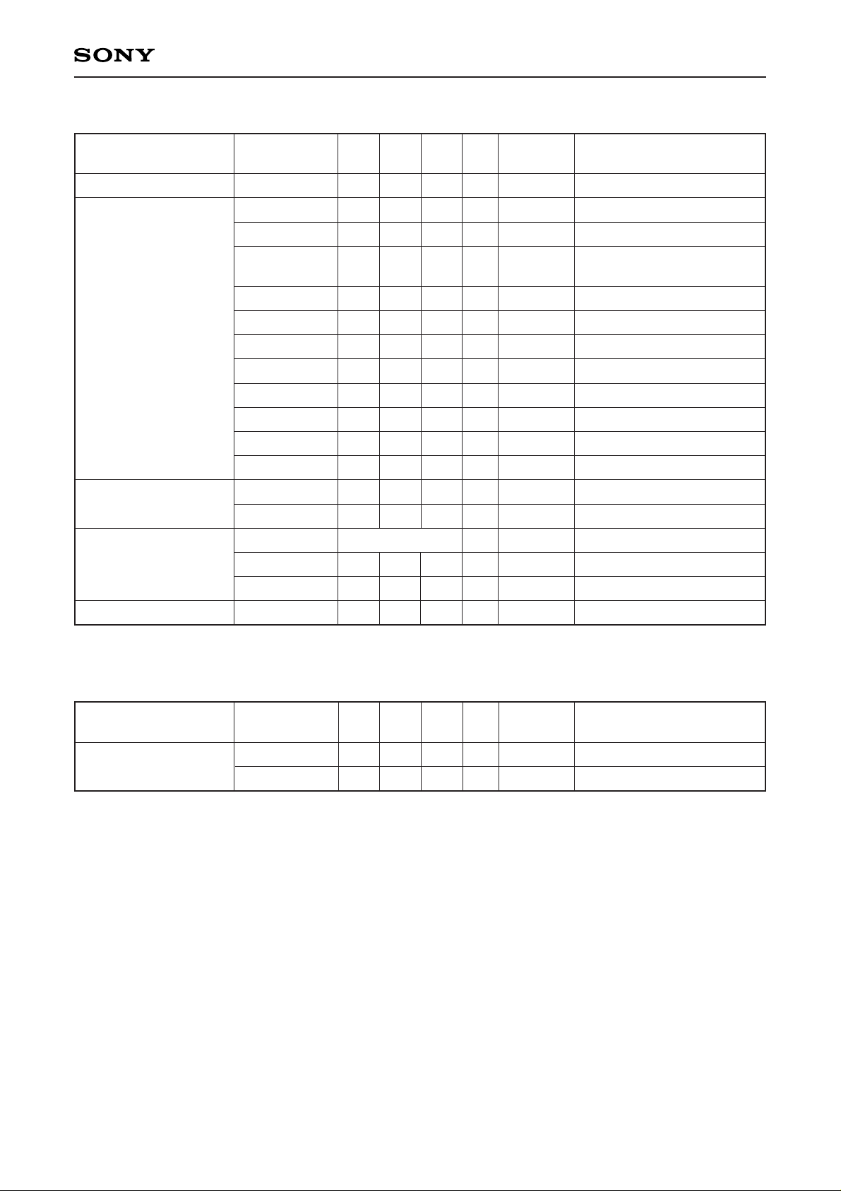
Absolute Maximum Ratings
ICX418ALB
Item
Substrate clock φSUB – GND
VDD, VRD, VDSUB, VOUT – GND
Supply voltage
VDD, VRD, VDSUB, VOUT – φSUB
Vφ1, Vφ2, Vφ3, Vφ4 – GND
Clock input voltage
1, Vφ2, Vφ3, Vφ4 – φSUB
Vφ
Voltage difference between vertical clock input pins
Voltage difference between horizontal clock input pins
Hφ1, Hφ2 – Vφ4
φRG – GND
φRG – φSUB
VL – φSUB
Pins other than GND and φSUB – VL
Storage temperature
Operating temperature
∗1
+27V (Max.) when clock width < 10µs, clock duty factor < 0.1%.
Ratings Unit Remarks
–0.3 to +50
–0.3 to +18
–55 to +10
–15 to +20
to +10
to +15
to +17
–17 to +17
–10 to +15
–55 to +10
–65 to +0.3
–0.3 to +30
–30 to +80
–10 to +60
V
V
V
V
V
V
V
V
V
V
V
V
°C
°C
1
∗
– 4 –
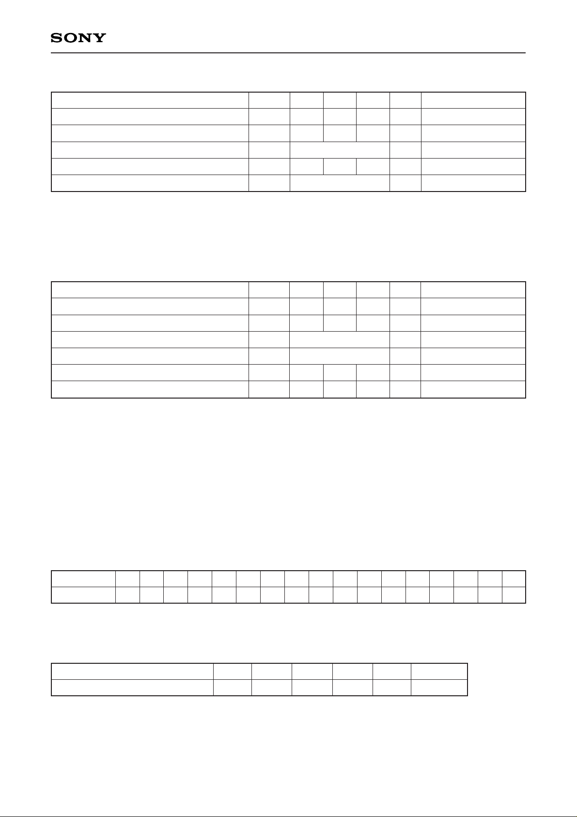
Bias Conditions 1 [when used in substrate bias internal generation mode]
ICX418ALB
Item
Output circuit supply voltage
Reset drain voltage
Protective transistor bias
Substrate bias circuit supply voltage
Substrate clock
∗1
VL setting is the VVL voltage of the ver tical transfer clock waveform, or the same supply voltage as the VL
Symbol
VDD
VRD
VL
VDSUB
φSUB
Min.
14.55
14.55
14.55
15.0
15.0
1
∗
15.0
2
∗
15.45
15.45
15.45
Unit
V
V
V
RemarksTyp. Max.
VRD = VDD
power supply for the V dr iver should be used. (When CXD1267AN is used.)
∗2
Do not apply a DC bias to the substrate clock pin, because a DC bias is generated within the CCD.
Bias Conditions 2 [when used in substrate bias external adjustment mode]
Item
Output circuit supply voltage
Reset drain voltage
Protective transistor bias
Substrate bias circuit supply voltage
Substrate voltage adjustment range
Substrate voltage adjustment precision
Symbol
VDD
VRD
VL
VDSUB
VSUB
∆VSUB
Min.
14.55
14.55
6.0
–3
15.0
15.0
3
∗
4
∗
15.45
15.45
14.0
+3
Unit
V
V
V
%
RemarksTyp. Max.
VRD = VDD
5
∗
5
∗
∗3
VL setting is the VVL voltage of the ver tical transfer clock waveform, or the same supply voltage as the VL
power supply for the V dr iver should be used. (When CXD1267AN is used.)
∗4
Connect to GND or leave open.
∗5
The setting value of the substrate voltage (VSUB) is indicated on the back of the image sensor by a
special code. When adjusting the substrate voltage externally, adjust the substrate voltage to the indicated
voltage. The adjustment precision is ±3%. However, this setting value has not significance when used in
substrate bias internal generation mode.
VSUB code — one character indication
Code and optimal setting correspond to each other as follows.
VSUB code
Optimal setting
6.0
f
E
6.5G7.0h7.5J8.0K8.5L9.0m9.5N10.0P10.5Q11.0
R
11.5
S
12.0
U
T
13.0V13.5W14.0
12.5
<Example> "L" → VSUB = 9.0V
DC Characteristics
Item
Output circuit supply current
Symbol
IDD
Min. Unit RemarksTyp. Max.
5.0
mA10.0
– 5 –
Clock V oltage Conditions
ICX418ALB
V
V
V
V
Vp-p
V
V
V
V
V
V
V
Vp-p
V
V
Vp-p
V
Vp-p
Waveform
diagram
1
2
2
2
2
2
2
2
2
2
2
2
3
3
4
4
4
5
Remarks
VVH = (VVH1 + VVH2)/2
VVL = (VVL3 + VVL4)/2
VφV = VVHn – VVLn (n = 1 to 4)
High-level coupling
High-level coupling
Low-level coupling
Low-level coupling
Low-level coupling
Item
Readout clock voltage
Vertical transfer clock
voltage
Horizontal transfer
clock voltage
Reset gate clock
voltage
∗1
Substrate clock voltage
∗1
Input the reset gate clock without applying a DC bias. In addition, the reset gate clock can also be driven
Symbol
VVT
VVH1, VVH2
VVH3, VVH4
VVL1, VVL2,
VVL3, VVL4
VφV
| VVH1 – VVH2 |
VVH3 – VVH
VVH4 – VVH
VVHH
VVHL
VVLH
VVLL
VφH
VHL
VRGL
VφRG
VRGLH – VRGLL
VφSUB
Min.
14.55
–0.05
–0.2
–9.6
8.3
–0.25
–0.25
4.75
–0.05
4.5
23.0
Typ.
15.0
0
0
–9.0
9.0
5.0
0
1
∗
5.0
24.0
Max. Unit
15.45
0.05
0.05
–8.5
9.65
0.1
0.1
0.1
0.5
0.5
0.5
0.5
5.25
0.05
5.5
0.8
25.0
with the following specifications.
Item
Reset gate clock
voltage
VRGL
VφRG
Symbol
Min.
–0.2
8.5
Typ.
0
9.0
– 6 –
Max. Unit
0.2
9.5
V
Vp-p
Waveform
diagram
4
4
Remarks
 Loading...