

Sony ICX406AQF Datasheet
ICX406A QF
Diagonal 8.98mm (Type 1/1.8) Frame Readout CCD Image Sensor with a Square Pixel for Color Cameras
Description
The ICX406AQF is a diagonal 8.98mm (Type 1/1.8)
interline CCD solid-state image sensor with a square
pixel array and 3.98M effective pixels. Frame readout
allows all pixels' signals to be output independently
within approximately 1/3.33 second.
Also, number of vertical pixels decimation allows
output of 30 frames per second in high frame rate
readout mode.
This chip features an electronic shutter with
variable charge-storage time.
R, G, B primary color mosaic filters are used as the
color filters, and at the same time high sensitivity and
low dark current are achieved through the adoption
of Super HAD CCD technology.
This chip is suitable for applications such as
electronic still cameras, etc.
Features
• Supprots frame readout
• High horizontal and vertical resolution
• Supports high frame rate readout mode: 30 frames/s, 25 frames/s,
AF1 mode: 60 frames/s, 50 frames/s,
AF2 mode: 120 frames/s, 100 frames/s
• Square pixel
• Horizontal drive frequency: 18MHz
• No voltage adjustments (reset gate and substrate bias are not adjusted.)
• R, G, B primary color mosaic filters on chip
• High sensitivity, low dark current
• Continuous variable-speed shutter
• Excellent anti-blooming characteristics
• Exit pupil distance recommended range –20 to –100mm
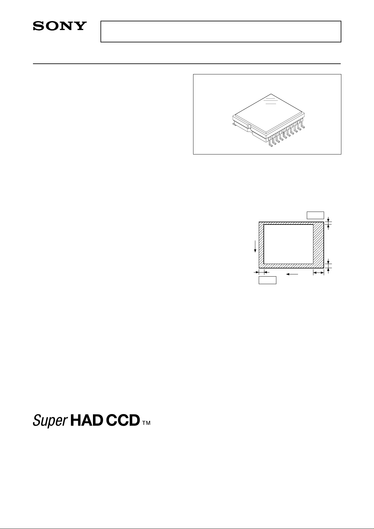
• 20-pin high-precision plastic package
Device Structure
• Interline CCD image sensor
• Total number of pixels: 2384 (H) × 1734 (V) approx. 4.13M pixels
• Number of effective pixels: 2312 (H) × 1720 (V) approx. 3.98M pixels
• Number of active pixels: 2308 (H) × 1712 (V) approx. 3.95M pixels diagonal 8.980mm
• Number of recommended recording pixels:
2272 (H) × 1740 (V) approx. 3.87M pixels diagonal 8.875mm aspect ratio 4:3
• Chip size: 8.10mm (H) × 6.64mm (V)
• Unit cell size: 3.125µm (H) × 3.125µm (V)
• Optical black: Horizontal (H) direction: Front 16 pixels, rear 56 pixels
Vertical (V) direction: Front 12 pixels, rear 2 pixels
• Number of dummy bits: Horizontal 28
Vertical 1 (even fields only)
• Substrate material: Silicon
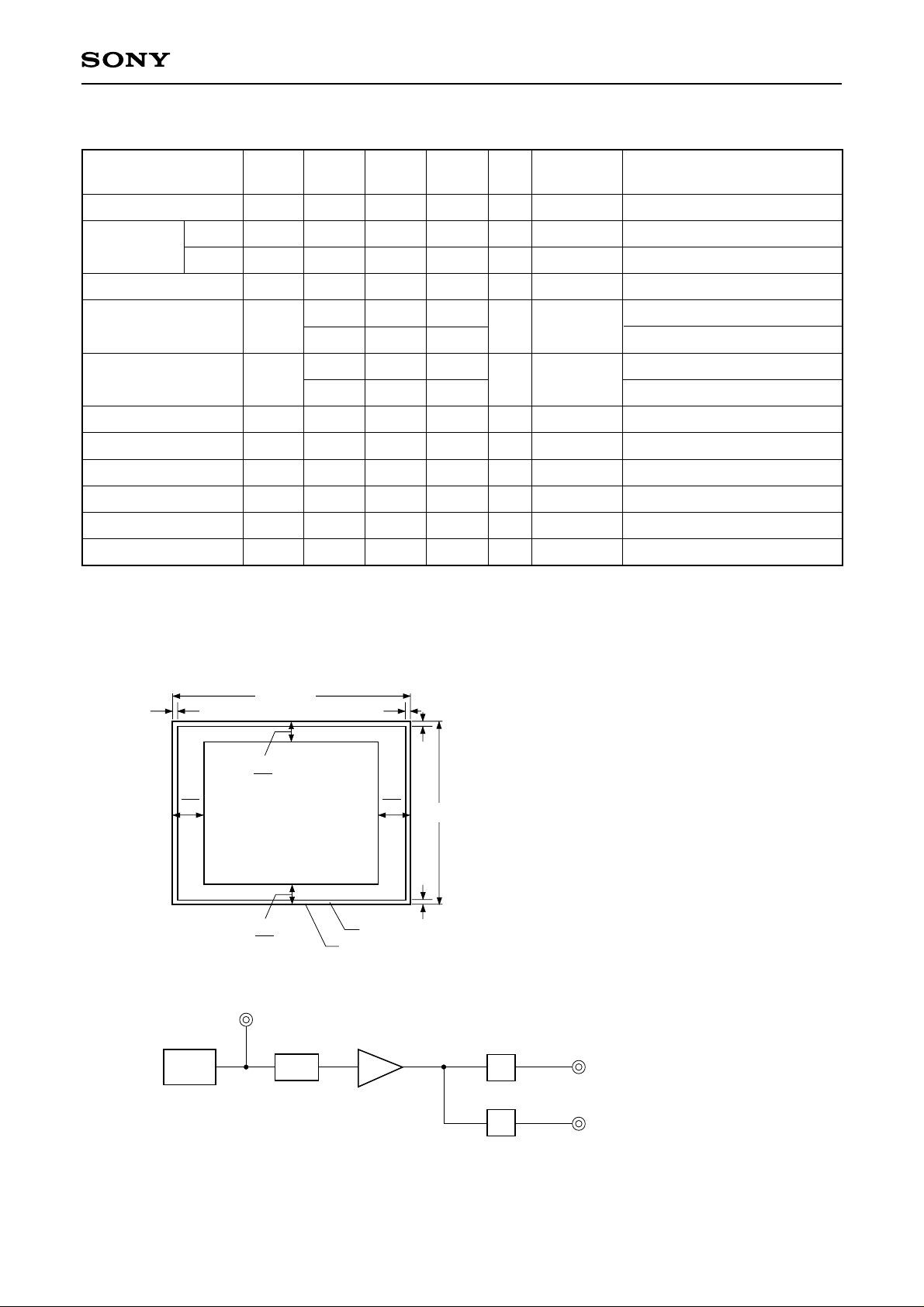
20 pin SOP (Plastic)
V
16
Pin 11
H
Optical black position
(T op View)
Pin 1
2
12
56
∗
Super HAD CCD is a trademark of Sony Corporation. The Super HAD CCD is a version of Sony's high performance CCD HAD (Hole-
Accumulation Diode) sensor with sharply improved sensitivity by the incorporation of a new semiconductor technology developed by Sony
Corporation.
Sony reserves the right to change products and specifications without prior notice. This information does not convey any license by
any implication or otherwise under any patents or other right. Application circuits shown, if any, are typical examples illustrating the
operation of the devices. Sony cannot assume responsibility for any problems arising out of the use of these circuits.
– 1 –
E01331-PS
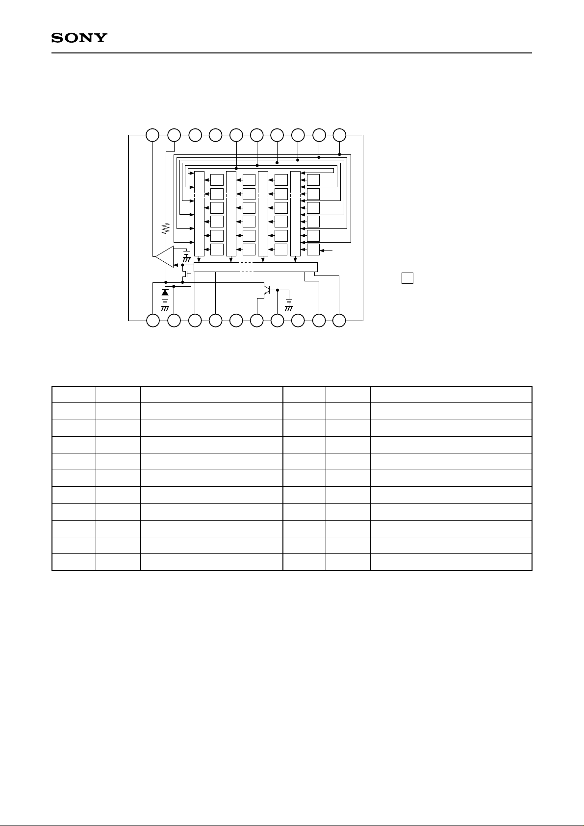
Block Diagram and Pin Configuration
(Top View)
OUT
V
GND
TEST
TEST
10 9 8 7 6 5 4 3 2 1
ICX406AQF
4
Vφ1BVφ1AVφ2Vφ3BVφ3AVφ
Gb
Gb
R
Gb
R
Gb
Vertical register
11 12 13 14 15 16 17 18 19 20
φRG
2Hφ1
Hφ
DD
V
B
φSUB
R
Gb
R
Gb
SUB
C
Gr
B
Gr
B
Horizontal register
GND
B
Gr
B
Gr
B
GrRGrR
Note)
Note) : Photo sensor
L
V
2
Hφ1Hφ
Pin Description
Pin No. Symbol Description Pin No. Symbol Description
1
2
3
4
Vφ4
Vφ3A
Vφ3B
Vφ2
Vertical register transfer clock
Vertical register transfer clock
Vertical register transfer clock
Vertical register transfer clock
11
12
13
14
VDD
φRG
Hφ2
Hφ1
Supply voltage
Reset gate clock
Horizontal register transfer clock
Horizontal register transfer clock
5
6
7
8
9
10
1
∗
Leave this pin open.
2
∗
DC bias is generated within the CCD, so that this pin should be grounded externally through a capacitance
Vφ1A
Vφ1B
TEST
TEST
GND
VOUT
Vertical register transfer clock
Vertical register transfer clock
1
Test pin
Test pin
∗
1
∗
GND
Signal output
15
16
17
18
19
20
GND
φSUB
CSUB
VL
Hφ1
Hφ2
GND
Substrate clock
2
Substrate bias
∗
Protective transistor bias
Horizontal register transfer clock
Horizontal register transfer clock
of 0.1µF.
– 2 –
Absolute Maximum Ratings
ICX406AQF
Item
DD, VOUT, φRG – φSUB
V
Vφ
1A, Vφ1B, Vφ3A, Vφ3B – φSUB
Against φSUB
Vφ2, Vφ4, VL – φSUB
Hφ1, Hφ2, GND – φSUB
CSUB – φSUB
VDD, VOUT, φRG, CSUB – GND
Against GND
Vφ1A, Vφ1B, Vφ2, Vφ3A, Vφ3B, Vφ4 – GND
Hφ1, Hφ2 – GND
Vφ1A, Vφ1B, Vφ3A, Vφ3B – VL
Against VL
Vφ2, Vφ4, Hφ1, Hφ2, GND – VL
Voltage difference between vertical clock input pins
Between input
clock pins
Hφ1 – Hφ2
Hφ1, Hφ2 – Vφ4
Storage temperature
Guaranteed temperature of performance
Operating temperature
Ratings Unit Remarks
–40 to +12
–50 to +15
–50 to +0.3
–40 to +0.3
–25 to
–0.3 to +22
–10 to +18
–10 to +6.5
–0.3 to +28
–0.3 to +15
to +15
–6.5 to +6.5
–10 to +16
–30 to +80
–10 to +60
–10 to +75
V
V
V
V
V
V
V
V
V
V
V
V
V
°C
°C
°C
1
∗
1
∗
+24V (Max.) when clock width < 10µs, clock duty factor < 0.1%.
+16V (Max.) is guaranteed for turning on or off power supply.
– 3 –
Bias Conditions
ICX406AQF
Item
Supply voltage
Protective transistor bias
Substrate clock
Reset gate clock
1
∗
VL setting is the VVL voltage of the vertical clock waveform, or the same voltage as the VL power supply
Symbol
VDD
VL
φSUB
φRG
Min.
14.55 15.45
15.0
1
∗
2
∗
2
∗
Unit RemarksTyp. Max.
V
for the V driver should be used.
2
∗
Do not apply a DC bias to the substrate clock and reset gate clock pins, because a DC bias is generated
within the CCD.
DC Characteristics
Item
Supply current
Symbol
IDD
Min. Unit RemarksTyp. Max.
7.0
mA10.03.0
Clock V olta ge Conditions
V
V
V
Waveform
Diagram
1
2
2
Remarks
VVH = (VVH1 + VVH2)/2
Item Symbol
Readout clock voltage
VVT
VVH1, VVH2
VVH3, VVH4
Min. Typ. Max. Unit
14.55
–0.05
–0.2
15.0
0
0
15.45
0.05
0.05
Vertical transfer clock
voltage
Horizontal transfer
clock voltage
Reset gate clock
voltage
Substrate clock voltage
VVL1, VVL2,
VVL3, VVL4
VφV
VVH3 – VVH
VVH4 – VVH
VVHH
VVHL
VVLH
VVLL
VφH
VHL
VCR
VφRG
VRGLH – VRGLL
VRGL – VRGLm
VφSUB
–8.0
6.8
–0.25
–0.25
4.75
–0.05
0.8
3.0
21.5
–7.5
7.5
5.0
0
2.5
3.3
22.5
–7.0
8.05
0.1
0.1
0.9
0.9
0.9
0.7
5.25
0.05
5.25
0.4
0.5
23.5
V
V
V
V
V
V
V
V
V
V
V
V
V
V
V
2
2
2
2
2
2
2
2
3
3
3
4
4
4
5
VVL = (VVL3 + VVL4)/2
VφV = VVHn – VVLn (n = 1 to 4)
High-level coupling
High-level coupling
Low-level coupling
Low-level coupling
Cross-point voltage
Low-level coupling
Low-level coupling
– 4 –
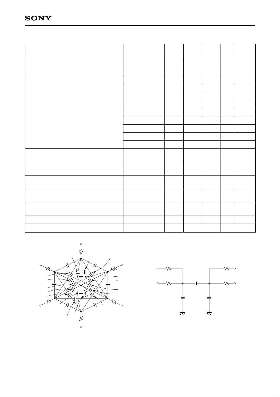
Clock Equivalent Circuit Constants
ICX406AQF
Item Min.
Capacitance between vertical transfer clock
and GND
Capacitance between vertical transfer
clocks
Capacitance between horizontal transfer
clock and GND
Capacitance between horizontal transfer
clocks
Capacitance between reset gate clock and
GND
Symbol
CφV1A, CφV3A
CφV1B, CφV3B
CφV2, CφV4
CφV1A2, CφV3A4
CφV1B2, CφV3B4
CφV23A, CφV41A
CφV23B, CφV41B
CφV1A3A
CφV1B3B
CφV1A3B, CφV1B3A
CφV24
CφV1A1B, CφV3A3B
CφH1, CφH2
CφHH
CφRG
Typ. Max.
1200
4700
3300
470
560
150
220
39
220
56
82
68
36
91
8
Unit Remarks
pF
pF
pF
pF
pF
pF
pF
pF
pF
pF
pF
pF
pF
pF
pF
Capacitance between substrate clock and
GND
Vertical transfer clock series resistor
Vertical transfer clock ground resistor
Horizontal transfer clock series resistor
Vφ
2
R
GND
2
Cφ
V1A3A
Cφ
Cφ
V3B4
R
4
V23A
Cφ
V3A4
Cφ
R
3A
Cφ
R
Cφ
Vφ
Cφ
Cφ
Cφ
Cφ
Vφ
1A
V1B2
V1A
Cφ
V1B3A
V1B
V41A
1B
V1A1B
R
1B
Cφ
V24
Cφ
V1A2
R
1A
Cφ
V4
Cφ
V41B
R
Cφ
V1B3B
V23B
3B
Vφ
Cφ
Cφ
V3A3B
Cφ
Cφ
Vφ
CφSUB
R1A, R1B, R2,
R3A, R3B, R4
RGND
RφH
3A
V2
V3A
V1A3B
V3B
3B
1000
62
18
15
Hφ1 Hφ2
CφHH
Hφ1 Hφ2
CφH1
pF
Ω
Ω
Ω
RφHRφH
RφHRφH
CφH2
Vφ
4
Vertical transfer clock equivalent circuit Horizontal transfer clock equivalent circuit
– 5 –
Drive Clock Waveform Conditions
(1) Readout clock waveform
100%
90%
V
VT
10%
0%
tr tf
twh
(2) Vertical transfer clock waveform
Vφ1A, Vφ1B Vφ3A, Vφ3B
V
VH1
V
VHH
V
VH
V
VHH
φM
ICX406AQF
φM
2
0V
V
V
VHH
VHH
V
VH
V
VHL
V
VHL
V
VL1
V
VLH
V
VLL
V
VL
V
Vφ2 Vφ4
V
VHH
V
VHL
V
VH2
V
VHH
V
VH
V
VHL
VL3
V
VHL
V
V
VH
V
VHL
V
VH3
VL
V
VHL
V
VLH
V
VLL
V
V
VHH
V
VH4
VHH
V
VHL
V
V
VL
VVH = (VVH1 + VVH2)/2
VVL = (VVL3 + VVL4)/2
VφV = VVHn – VVLn (n = 1 to 4)
VLL
V
V
VLH
V
VL2
V
VL4
VLH
V
VLL
V
VL
– 6 –
ICX406AQF
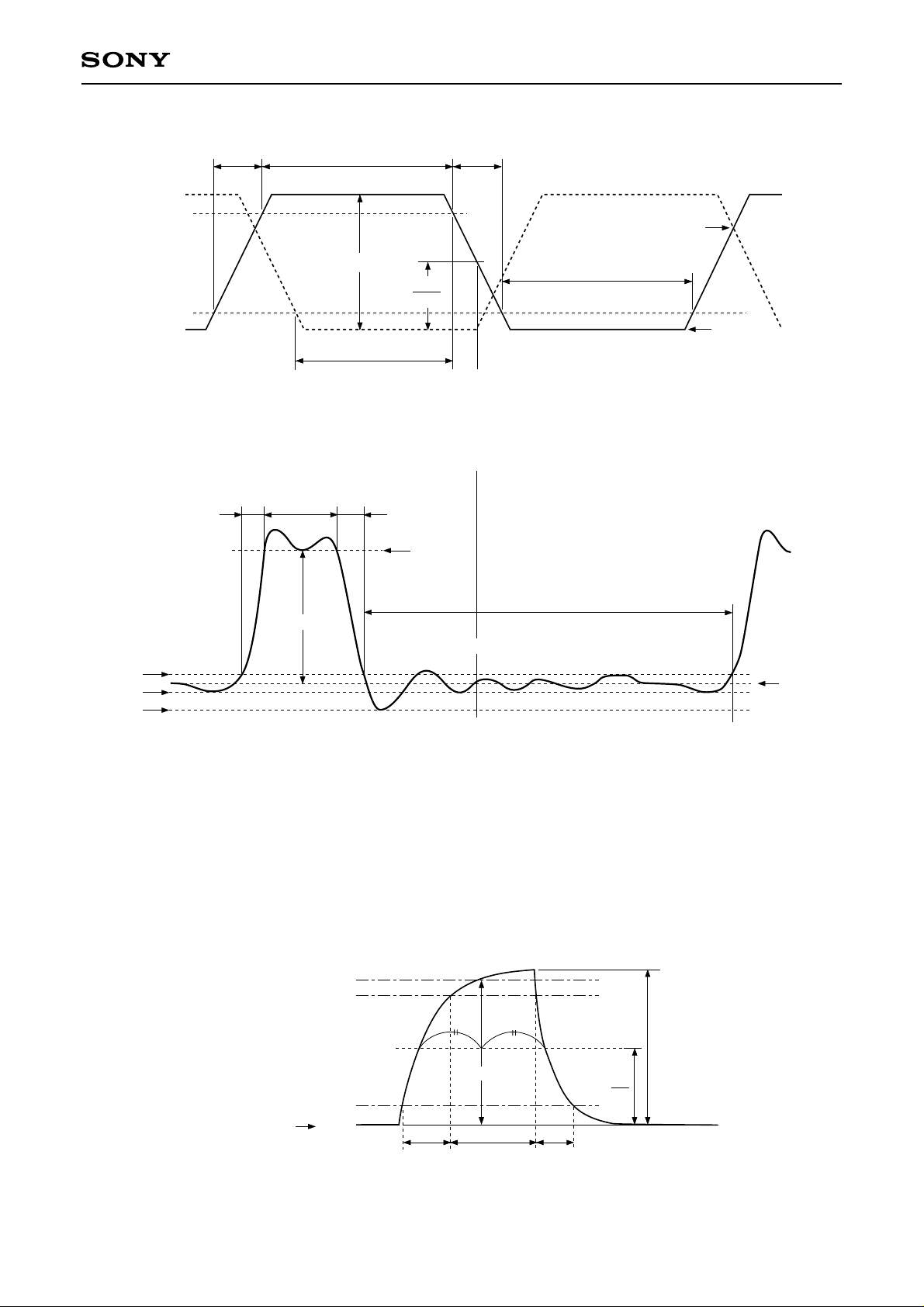
(3) Horizontal transfer clock waveform
tf
VCR
twl
VHL
Hφ
90%
10%
Hφ
tr
2
1
twh
Vφ
H
VφH
2
two
Cross-point voltage for the Hφ1 rising side of the horizontal transfer clocks Hφ1 and Hφ2 waveforms is VCR.
The overlap period for twh and twl of horizontal transfer clocks Hφ1 and Hφ2 is two.
(4) Reset gate clock waveform
RG waveform
V
RGLH
V
RGLL
V
RGLm
tr twh
Vφ
RG
tf
V
RGH
twl
Point A
V
RGL
VRGLH is the maximum value and VRGLL is the minimum value of the coupling waveform during the period from
Point A in the above diagram until the rising edge of RG.
In addition, VRGL is the average value of VRGLH and VRGLL.
VRGL = (VRGLH + VRGLL)/2
Assuming VRGH is the minimum value during the interval with twh, then:
VφRG = VRGH – VRGL
Negative overshoot level during the falling edge of RG is VRGLm.
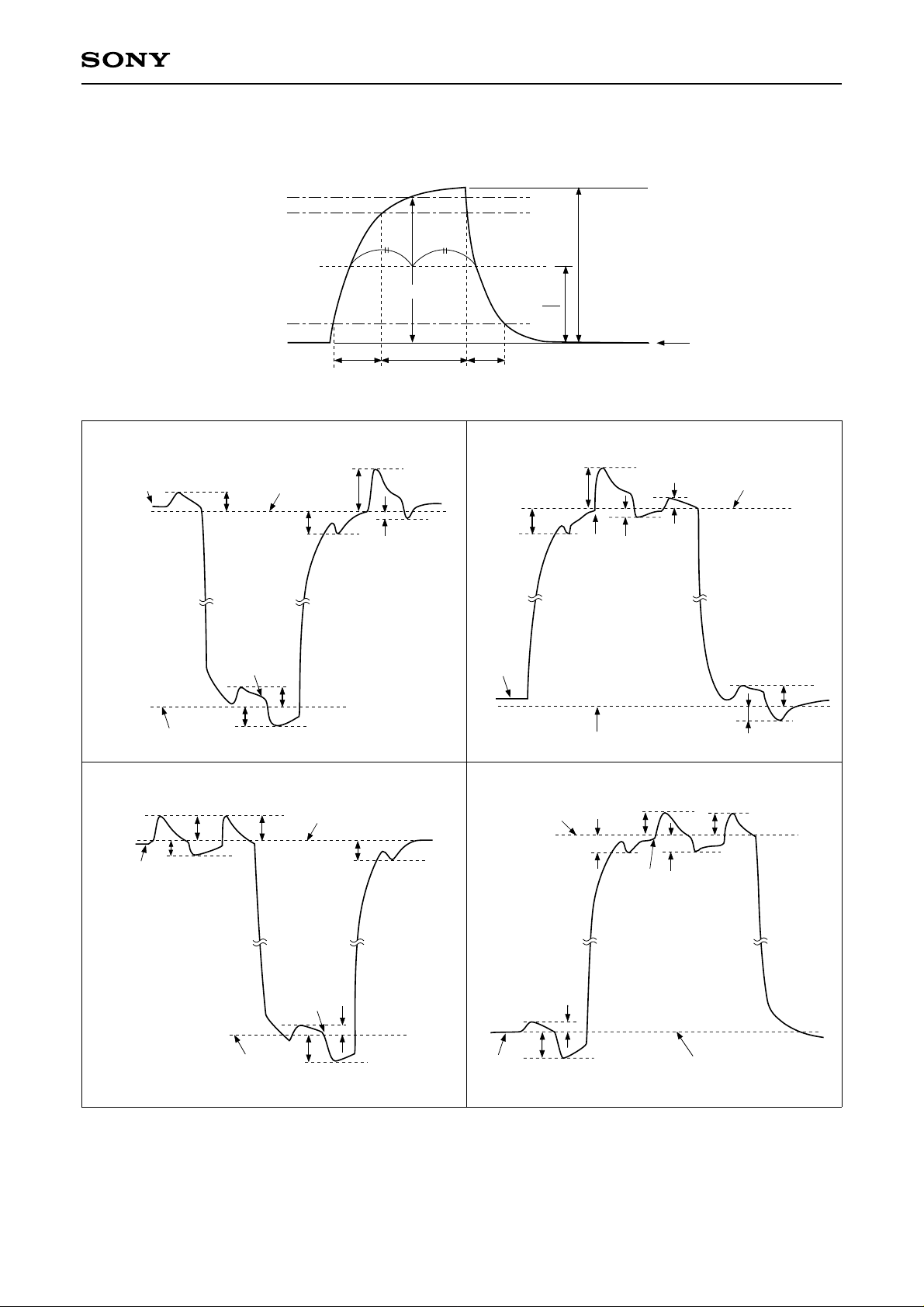
(5) Substrate clock waveform
100%
90%
10%
V
(A bias generated within the CCD)
SUB
0%
Vφ
SUB
tr tftwh
– 7 –
φM
φM
2
Clock Switching Characteristics (Horizontal drive frequency: 18MHz)
ICX406AQF
Item
Readout clock
Vertical transfer
clock
Horizontal
transfer clock
Reset gate clock
Substrate clock
Symbol
VT
Vφ1A, Vφ1B,
Vφ2, Vφ3A,
Vφ3B, Vφ4
Hφ1
Hφ2
φRG
φSUB
Horizontal transfer clock
Min.
3.10
14
14
7
1.6
Symbol
Hφ1, Hφ2
twh
twl tr tf
Typ. Max. Min. Typ. Max. Min. Typ. Max. Min. Typ. Max.
3.33
19.5
19.5
10
3.56
141419.5
19.5
37
0.5
8.5
8.5
4
14
14
0.5
15
0.5
8.5
8.5
5
250
14
14
0.5
two
Min.
Typ. Max.
UnitnsRemarksItem
12 19.5
Unit
µs
During readout
When using
ns
CXD3400N
ns
tf ≥ tr – 2ns
ns
During drain
µs
charge
Remarks
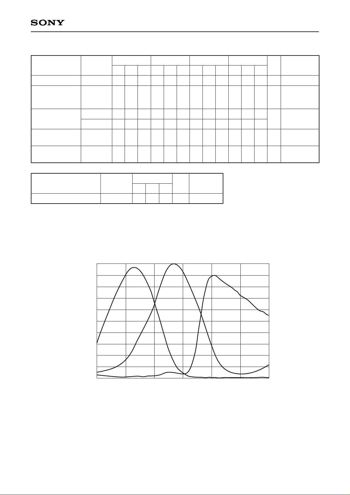
Spectral Sensitivity Characteristics (excludes lens characteristics and light source characteristics)
1.0
0.9
0.8
0.7
0.6
0.5
0.4
Relative Response
0.3
0.2
0.1
0
400
B
450 500 550
G
R
600 650 700
Wave Length [nm]
– 8 –
ICX406AQF
Image Sensor Characteristics (horizontal drive frequency: 18MHz) (Ta = 25°C)
Item
G Sensitivity
Sensitivity
comparison
Saturation signal
Smear
Symbol
Sg
R
B
Rr
Rb
Vsat
Min.
180
0.35
0.40
380
Typ.
220
0.50
0.55
–85
Max.
285
0.65
0.70
–81.2
Sm
–72
–68.0
20
Video signal shading
SHg
25
Dark signal
Dark signal shading
Line crawl G
Line crawl R
Line crawl B
Lag
1
∗
After closing the mechanical shutter, the smear can be reduced to below the detection limit by performing
Vdt
∆Vdt
Lcg
Lcr
Lcb
Lag
16
8
3.8
3.8
3.8
0.5
Measurement
Unit
method
mV
mV
dB
%
mV
mV
%
%
%
%
Remarks
1
1/30s accumulation
1
1
2
Ta = 60°C
Frame readout mode
∗
3
High frame rate readout mode
Zone 0 and I
4
Zone 0 to II'
5
6
Ta = 60°C, 3.33 frame/s
Ta = 60°C, 3.33 frame/s,
7
7
7
8
vertical register sweep operation.
2
∗
Excludes vertical dark signal shading caused by vertical register high-speed transfer.
1
2
∗
Zone Definition of Video Signal Shading
2
H
8
2312 (H)
V
10
V
10
Zone 0, I
Zone II, II'
Ignored region
Effective pixel region
Measurement System
CCD signal output [∗A]
CCD C.D.S
AMP
2
4
H
8
1720 (V)
4
S/H
Gr/Gb channel signal output [∗B]
S/H
R/B channel signal output [∗C]
Note) Adjust the amplifier gain so that the gain between [∗A] and [∗B], and between [∗A] and [∗C] equals 1.
– 9 –
ICX406AQF
Image Sensor Characteristics Measurement Method
Measurement conditions
(1) In the following measurements, the device drive conditions are at the typical values of the bias and clock
voltage conditions, and the frame readout mode is used.
(2) In the following measurements, spot blemishes are excluded and, unless otherwise specified, the optical
black level (OB) is used as the reference for the signal output, which is taken as the value of the Gr/Gb
channel signal output or the R/B channnel signal output of the measurement system.
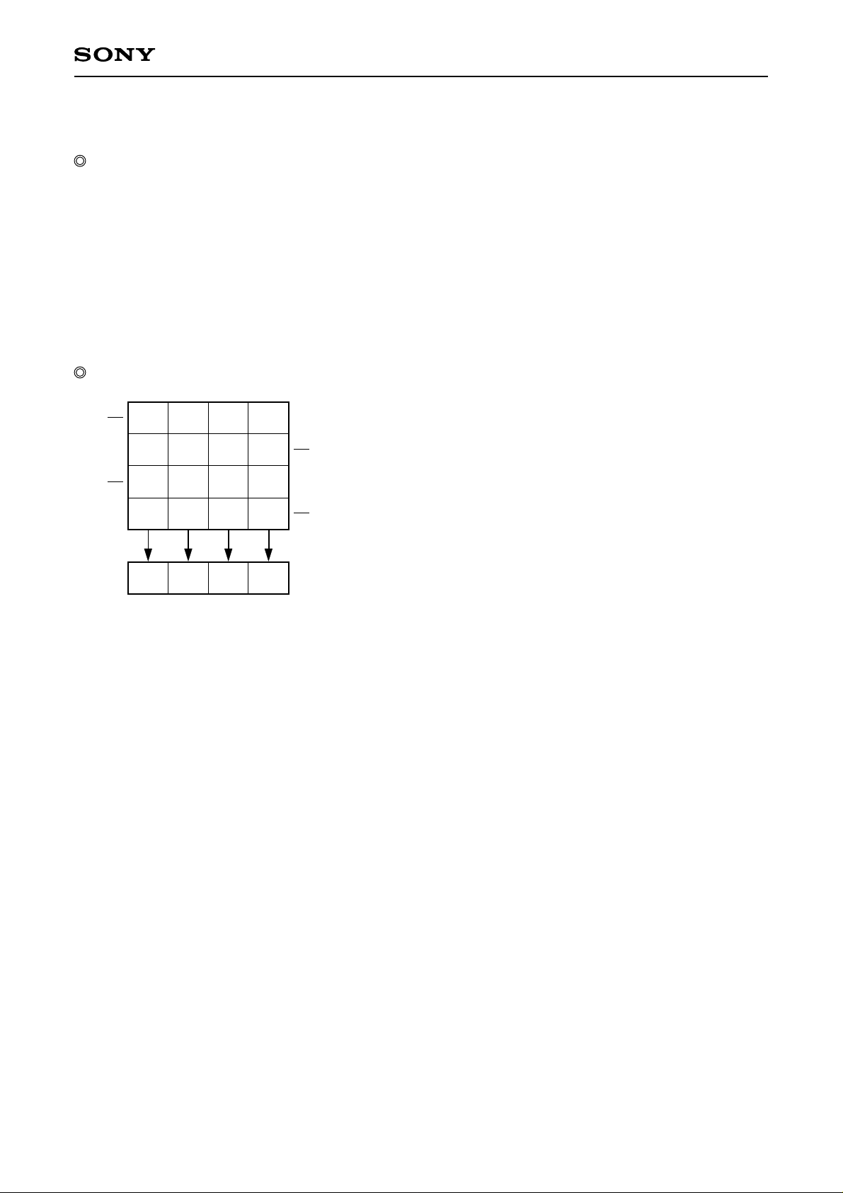
Color coding of this image sensor & Readout
B2
B1
Gb B Gb B
RGrRGr
Gb B Gb B
RGrRGr
Color Coding Diagram
The primary color filters of this image sensor are arranged in
the layout shown in the figure on the left (Bayer arrangement).
A2
Gr and Gb denote the G signals on the same line as the R
signal and the B signal, respectively.
For frame readout, the A1 and A2 lines are output as signals in
A1
the A field, and the B1 and B2 lines in the B field.
Horizontal register
– 10 –
 Loading...