

Sony ICX285AL Datasheet
ICX285AL
Diagonal 11 mm (Type 2/3) Progressive Scan CCD Image
Sensor with Square Pixel for B/W Cameras
Description
The ICX285AL is a diagonal 11 mm (Type 2/3)
interline CCD solid-state image sensor with a square
pixel array. High sensitivity and low smear are
achieved through the adoption of EXview HAD CCD
technology. Progressive scan allows all pixel’s signals
to be output independently within approximately
1/15 second. Also, the adoption of high frame rate
readout mode supports 60 frames per second. This
chip features an electronic shutter with variable
charge-storage time which makes it possible to realize
full-frame still images without a mechanical shutter.
This chip is suitable for image input applications
such as still cameras which require high resolution,
etc.
Features
• Progressive scan allo ws individual readout of the image signals from all pix els.
• High horizontal and vertical resolution (both approximately 1024 TV-lines) still images without a mechanical
shutter
• Supports high frame rate readout mode (effective 256 lines output, 60 frame/s)
• Square pixel
• Aspect ratio: 4:3
• Horizontal drive frequency: 28.64 MHz
• High sensitivity, low smear
• Low dark current, excellent anti-blooming characteristics
• Continuous variable-speed shutter
• Horizontal register: 5.0 V driv e
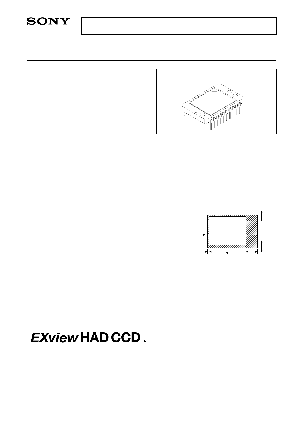
20 pin DIP (Ceramic)
Pin 1
2
V
Device Structure
• Interline CCD image sensor
• Image size: Diagonal 11 mm (Type 2/3)
• Total number of pixels: 1434 (H) × 1050 (V) approx. 1.50M pixels
• Number of effective pixels:1392 (H) × 1040 (V) approx. 1.45M pixels
• Number of active pixels: 1360 (H) × 1024 (V) approx. 1.40M pixels
• Chip size: 10.2 mm (H) × 8.3 mm (V)
• Unit cell size: 6.45 µm (H) × 6.45 µm (V)
• Optical black: Horizontal (H) direction: Front 2 pixels, rear 40 pixels
Vertical (V) direction: Front 8 pixels, rear 2 pixels
• Number of dummy bits: Horizontal 20
V ertical 3
• Substrate material: Silicon
* EXview HAD CCD is a trademark of Sony Corporation.
EXview HAD CCD is a CCD that drastically improves light efficiency by including near infrared light region as a basic structure of
HAD (Hole-Accumulation-Diode) sensor.
Sony reserves the right to change products and specifications without prior notice. This information does not convery any license by
any implication or otherwise under any patents or other right. Application circuits shown, if any, are typical examples illustrating the
operation of the devices. Sony cannot assume responsibility for any problems arising out of the use of these circuits.
– 1 –
2
Pin 11
Optical black position
H
(T op View)
40
E00Y42A27
8
Block Diagram and Pin Configuration (Top View)
ICX285AL
Pin Description
GND
GND
Vφ3Vφ4NC
10 9 8 7 6 5 4 3 2 1
Vertical register
Horizontal register
11 12 13 14 15 16 17 18 19 20
OUT
V
DD
V
φRG
2Hφ1
Hφ
NC
φSUB
Vφ2BNC
L
V
SUB
C
Vφ2AVφ
Note)
Hφ1Hφ
1
Note) : Photo sensor
2
Pin No.
1
2
3
4
5
6
7
8
9
10
*1
DC bias is generated within the CCD , so that this pin should be grounded externally through a capacitance of
Symbol
Vφ1
Vφ2A
NC
Vφ2B
NC
NC
Vφ4
Vφ3
GND
GND
Vertical register transfer clock
Vertical register transfer clock
Vertical register transfer clock
Vertical register transfer clock
Vertical register transfer clock
GND
GND
Description
Pin No.
11
12
13
14
15
16
17
18
19
20
Symbol
VOUT
VDD
φRG
Hφ2
Hφ1
φSUB
CSUB
VL
Hφ1
Hφ2
Description
Signal output
Supply voltage
Reset gate clock
Horizontal register transfer clock
Horizontal register transfer clock
Substrate clock
Substrate bias
*1
Protective transistor bias
Horizontal register transfer clock
Horizontal register transfer clock
0.1µF.
– 2 –
Absolute Maximum Ratings
ICX285AL
Item
VDD, VOUT, φRG – φSUB
Vφ2A, Vφ2B – φSUB
Against φSUB Vφ1, Vφ3, Vφ4, VL – φSUB
Hφ1, Hφ2, GND – φSUB
CSUB – φSUB
VDD, VOUT, φRG, CSUB – GND
Against GND Vφ1, Vφ2A, Vφ2B, Vφ3, Vφ4 – GND
Hφ1, Hφ2 – GND
Vφ2A, Vφ2B – VL
Against VL
Vφ1, Vφ3, Vφ4, Hφ1, Hφ2, GND – VL
Voltage difference between vertical clock input pins
Between input
clock pins
Hφ1 – Hφ2
Hφ1, Hφ2 – Vφ4
Storage temperature
Performance guarantee temperature
Operating temperature
Ratings
–40 to +12
–50 to +15
–50 to +0.3
–40 to +0.3
–25 to
–0.3 to +22
–10 to +18
–10 to +6.5
–0.3 to +28
–0.3 to +15
to +15
–6.5 to +6.5
–10 to +16
–30 to +80
–10 to +60
–10 to +75
Unit
V
V
V
V
V
V
V
V
V
V
V
V
V
°C
°C
°C
Remarks
*1
*1
+24 V (Max.) when clock width < 10 µs, clock duty factor < 0.1%.
+16 V (Max.) is guaranteed for power-on and power-off.
Bias Conditions
Item
Supply voltage
Protective transistor bias
Substrate clock
Reset gate clock
Symbol
VDD
VL
φSUB
φRG
Min.
14.55
Typ.
15.0
*2
*3
*3
Max.
15.45
UnitVRemarks
DC characteristics
Item
Supply current
*2
VL setting is the VVL voltage of the vertical clock waveform, or the same v oltage as the VL power supply for the
Symbol
IDD
Min. Typ .
9
Max.
11
UnitmARemarks
V driver should be used.
*3
Do not apply a DC bias to the substrate clock and reset gate clock pins , because a DC bias is generated within
the CCD.
– 3 –
Clock V oltage Conditions
ICX285AL
Item
Readout clock voltage
Vertical transfer
clock voltage
Horizontal transfer
clock voltage
Reset gate
clock voltage
Symbol
VVT
VVH1, VVH2
VVH3, VVH4
VVL1, VVL2,
VVL3, VVL4
VφV
VVH3 – VVH
VVH4 – VVH
VVHH
VVHL
VVLH
VVLL
VφH
VHL
VCR
VφRG
VRGLH – VRGLL
VRGL – VRGLm
Min.
14.55
–0.05
–0.2
–7.3
6.5
–0.25
–0.25
4.75
–0.05
VφH/2
3.0
Typ.
15.0
0
0
–7.0
7.0
5.0
0
3.3
Max.
15.45
0.05
0.05
–6.7
7.35
0.1
0.1
1.4
1.3
1.4
0.8
5.25
0.05
5.5
0.4
0.5
Unit
V
V
V
V
V
V
V
V
V
V
V
V
V
V
V
V
V
Waveform
diagram
1
2
2
2
2
2
2
2
2
2
2
3
3
3
4
4
4
Remarks
VVH = (VVH1 + VVH2)/2
VVL = (VVL3 + VVL4)/2
VφV = VVHn – VVLn (n = 1 to 4)
High-level coupling
High-level coupling
Low-level coupling
Low-level coupling
Cross-point voltage
Low-level coupling
Low-level coupling
Substrate clock voltage
VφSUB
21.25
22.0
22.75
V
5
– 4 –
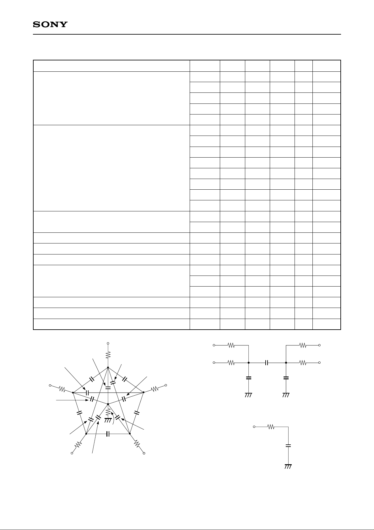
Clock Equivalent Circuit Constants
ICX285AL
Item
Capacitance between vertical transfer clock and GND
Capacitance between vertical transfer clocks
Capacitance between horizontal transfer clock and GND
Capacitance between horizontal transfer cloc ks
Symbol
CφV1
CφV2A
CφV2B
CφV3
CφV4
CφV12A
CφV12B
CφV2A3
CφV2B3
CφV14
CφV34
CφV2A4
CφV2B4
CφH1
CφH2
CφHH
Typ.
5600
6800
22000
8200
22000
150
390
270
470
2200
330
390
560
47
39
74
Max. Unit
pF
pF
pF
pF
pF
pF
pF
pF
pF
pF
pF
pF
pF
pF
pF
pF
RemarksMin.
Capacitance between reset gate clock and GND
Capacitance between substrate clock and GND
Vertical transfer clock series resistor
Vertical transfer clock ground resistor
Horizontal transfer clock series resistor
Reset gate clock ground resistor
Vφ
4
Cφ
Vφ
Cφ
V4
Cφ
V12B
Cφ
V41
R
1
1
V1
Cφ
V12A
Cφ
V2A4
R
2A
Cφ
Vφ
2A
V2A
Cφ
R
V2A3
R
GND
4
Cφ
V34
Cφ
V2B4
Cφ
V2B
R
2B
Cφ
V2B3
Cφ
V3
R
3
Vφ
3
Vφ
2B
CφRG
CφSUB
R1, R3
R2A, R2B
R4
RGND
RφH
RφRG
Hφ
1
Hφ
1
Rφ
Rφ
H
H
Cφ
4
1300
30
32
20
60
7.5
24
Cφ
HH
H1
Cφ
pF
pF
Ω
Ω
Ω
Ω
Ω
Ω
Rφ
H
Rφ
H
H2
Horizontal transfer clock equivalent cir cuit
Rφ
RGφ
RG
Cφ
RG
Hφ
Hφ
2
2
Vertical transfer cloc k equivalent circuit
– 5 –
Reset gate clock equivalent circuit
Drive Clock Waveform Conditions
(1) Readout clock wavef orm
100%
90%
10%
0%
(2) Vertical transfer clock waveform
Vφ
1
V
V
VH
VHH
V
V
VT
tr tf
VHH
twh
Vφ
ICX285AL
φM
φM
2
0V
3
V
VHH
V
VHH
V
VH
V
VL1
Vφ2A, Vφ
V
VH2
V
VHL
V
VHL
V
Vφ
VH3
V
VLH
V
VL3
V
V
4
V
VHH
V
VHL
V
VH4
VLL
VL
V
VHH
V
VHL
V
VH
V
VHL
V
VLH
V
VLL
2B
V
VHH
V
VH1
VH
V
VHL
VHL
V
VL
V
VHH
V
VHL
V
V
V
VL2
V
VLH
V
VLL
V
VL
VVH = (VVH1 + VVH2)/2
VVL = (VVL3 + VVL4)/2
VφV = VVHn – VVLn (n = 1 to 4)
– 6 –
V
VL4
V
VLL
V
VL
V
VLH
(3) Horizontal transfer clock waveform
ICX285AL
tf
VCR
twl
VHL
Hφ
90%
10%
Hφ
tr
2
1
twh
Vφ
H
VφH
2
two
Cross-point voltage for the Hφ1 rising side of the horizontal transfer clocks Hφ1 and Hφ2 waveforms is VCR.
The overlap period for twh and twl of horizontal transf er clocks Hφ1 and Hφ2 is two.
(4) Reset gate clock waveform
RG waveform
tr twh
Vφ
RG
tf
V
RGH
twl
Point A
V
V
V
RGLH
RGLL
RGLm
V
RGL
VRGLH is the maximum value and VRGLL is the minimum value of the coupling waveform during the period from
Point A in the abo ve diagram until the rising edge of RG.
In addition, VRGL is the average value of VRGLH and VRGLL.
VRGL = (VRGLH + VRGLL)/2
Assuming VRGH is the minimum value during the interval twh, then:
VφRG = VRGH – VRGL
Negative overshoot level during the falling edge of RG is VRGLm.
(5) Substrate clock waveform
100%
90%
φM
Vφ
SUB
10%
V
SUB
0%
tr tftwh
φM
2
(A bias generated within the CCD)
– 7 –
 Loading...