

ICX282AKF
Diagonal 11mm (Type 2/3) Frame Readout CCD Image Sensor with Square Pixel for Color Cameras
Description
The ICX282AKF is a diagonal 11mm (Type 2/3)
interline CCD solid-state image sensor with a square
pixel array and 5.07M effective pixels. Frame readout
allows all pixels' signals to be output independently
within approximately 1/3.75 second. In addition, output
is possible using various addition and pulse elimination
methods. This chip features an electronic shutter with
variable charge-storage time. Adoption of a design
specially suited for frame readout ensures a saturation
signal level equivalent to that when using field readout.
High resolution and high color reproductively are
achieved through the use of Ye, Cy, Mg and G
complementary color mosaic filters as the color filters.
Further, high sensitivity and low dark current are
achieved through the adoption of Super HAD CCD
technology.
This chip is suitable for applications such as
electronic still cameras, PC input cameras, etc.
Features
• High horizontal and vertical resolution
• Supports 10 types of readout modes
Frame readout mode, 2× speed mode (1), 2× speed mode (2), 8× speed mode,
center scan mode (1), center scan mode (2), center scan mode (3),
center scan mode (4), AF mode (1), AF mode (2)
• Square pixel
• Horizontal drive frequency: 22.5MHz
• No voltage adjustments (reset gate and substrate bias are not adjusted.)
• Ye, Cy, Mg and G complementary color mosaic filters on chip
• High sensitivity, low dark current, excellent anti-blooming characteristics
• Continuous variable-speed shutter
• Horizontal register, reset gate: 3.3V drive
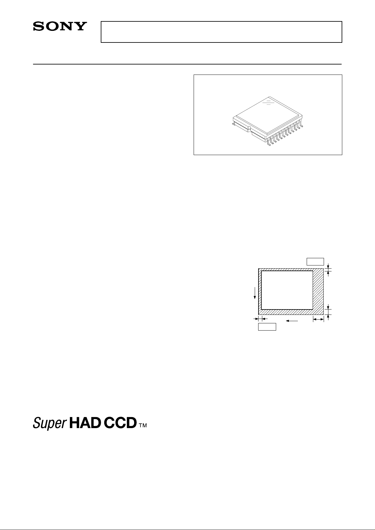
• 24-pin high-precision plastic package
Device Structure
• Interline CCD image sensor
• Image size: Diagonal 11mm (Type 2/3)
• Total number of pixels: 2658 (H) × 1970 (V) approx. 5.24M pixels
• Number of effective pixels:2588 (H) × 1960 (V) approx. 5.07M pixels
• Number of active pixels: 2580 (H) × 1944 (V) approx. 5.02M pixels
• Number of recommended recording pixels:
2560 (H) × 1920 (V) approx. 4.92M pixels
• Chip size: 9.74mm (H) × 7.96mm (V)
• Unit cell size: 3.4µm (H) × 3.4µm (V)
• Optical black: Horizontal (H) direction: Front 12 pixels, rear 58 pixels
Vertical (V) direction: Front 8 pixels, rear 2 pixels
• Number of dummy bits: Horizontal 28
Vertical 1 (even fields only)
• Substrate material: Silicon
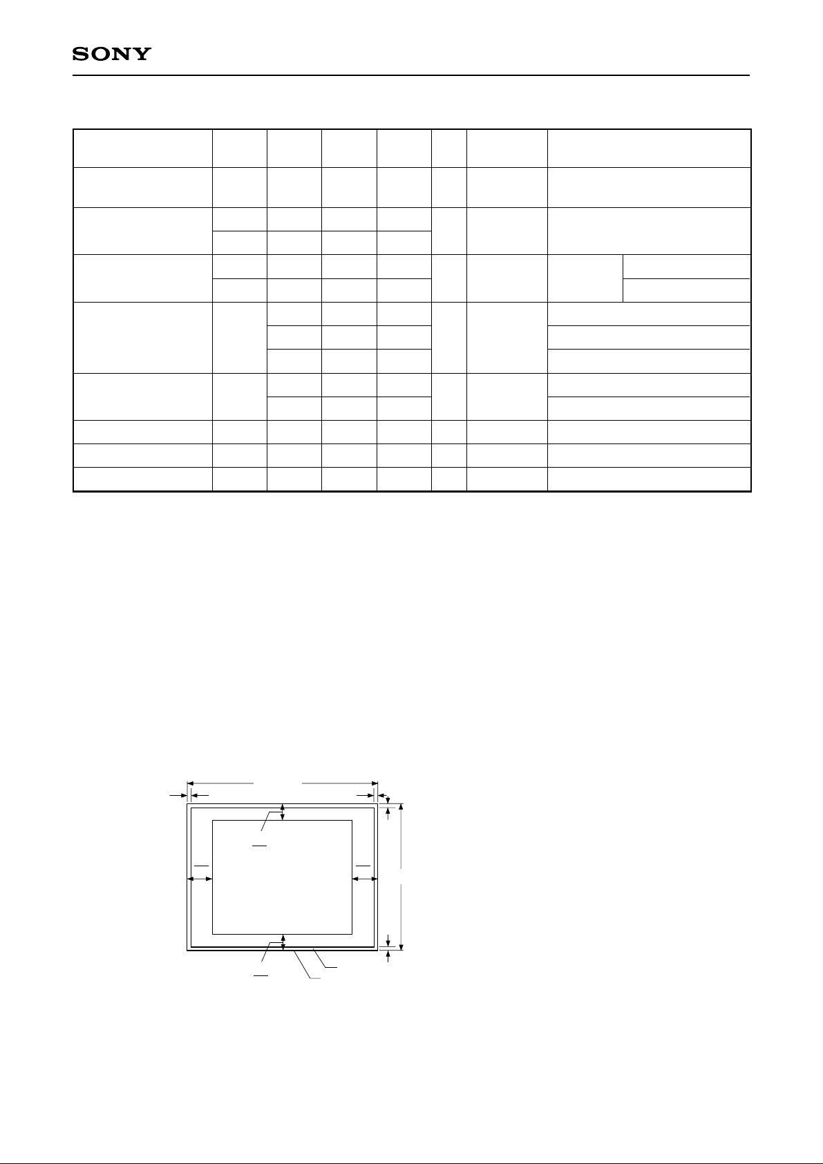
24 pin SOP (Plastic)
V
12
Pin 13
H
Optical black position
(T op View)
Pin 1
58
2
8
∗
Super HAD CCD is a registered trademark of Sony Corporation. Super HAD CCD is a CCD that drastically improves sensitivity by introducing
newly developed semiconductor technology by Sony Corporation into Sony's high-performance HAD (Hole-Accumulation Diode) sensor.
Sony reserves the right to change products and specifications without prior notice. This information does not convey any license by
any implication or otherwise under any patents or other right. Application circuits shown, if any, are typical examples illustrating the
operation of the devices. Sony cannot assume responsibility for any problems arising out of the use of these circuits.
– 1 –
E01628-PS
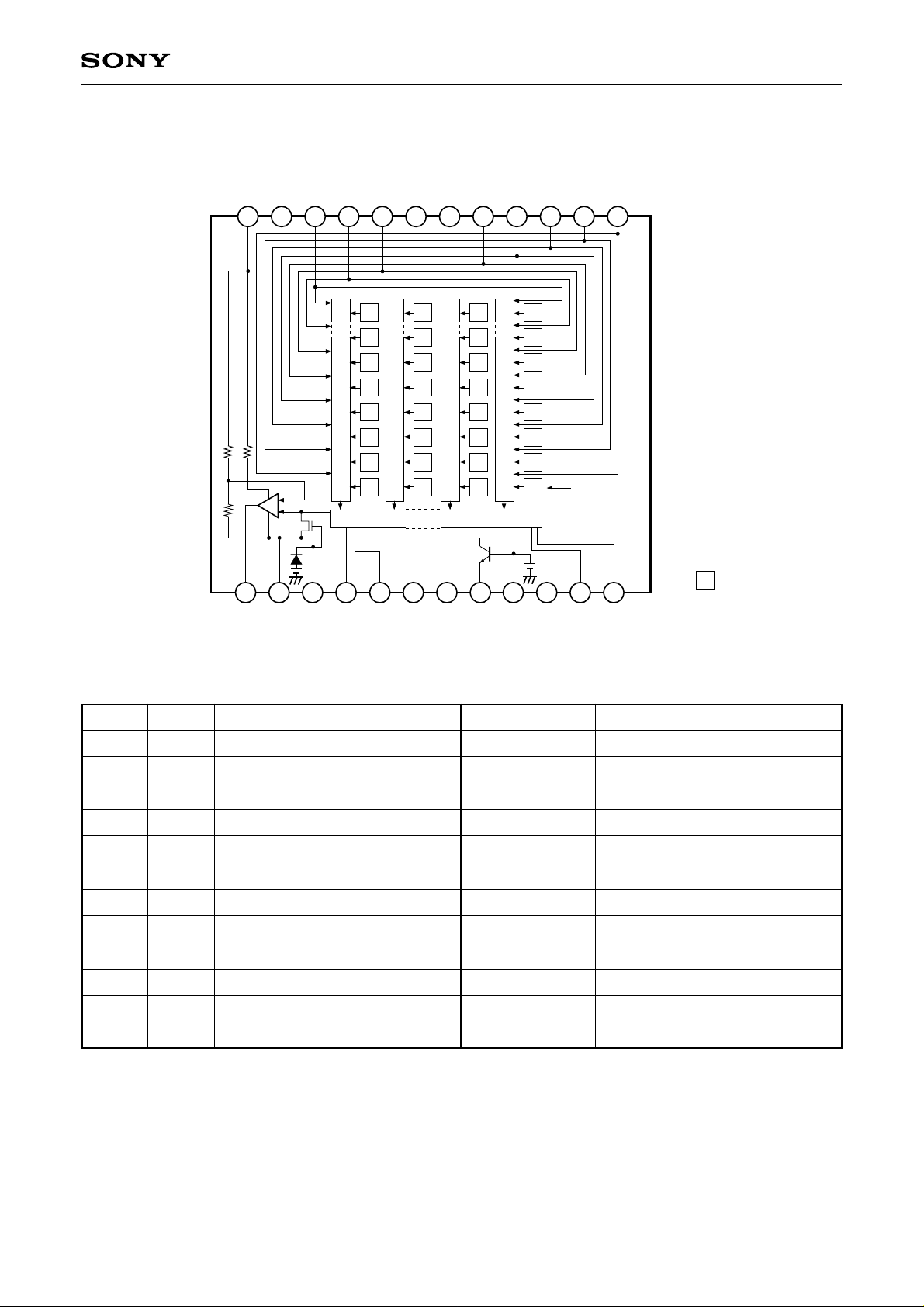
Block Diagram and Pin Configuration
(Top View)
1C
Vφ
GND
GND
12 11 10 9 8 7 6 5 4 3 2 1
ICX282AKF
1A
1B
Vφ
Vφ
NC
NC
2
Vφ
3B
3C
Vφ
Vφ
4
3A
Vφ
Vφ
Ye
G
Ye
G
Ye
G
Vertical register
Ye
G
13 14 15 16 17 18 19 20 21 22 23 24
OUT
V
DD
V
φRG
2B
Hφ
Cy
Mg
Cy
Mg
Cy
Mg
Cy
Mg
Horizontal register
1B
Hφ
GND
NC
Ye
Ye
Ye
Ye
G
G
G
G
φSUB
SUB
C
Cy
Mg
Cy
Mg
Cy
Mg
Cy
Mg
Note)
Note)
L
V
2A
1A
Hφ
Hφ
: Photo sensor
Pin Description
Pin No. Symbol Description Pin No. Symbol Description
1
Vφ4
Vertical register transfer clock
13
VOUT
Signal output
2
Vφ3A
3
Vφ3B
4
Vφ3C
5
Vφ2
6
NC
7
NC
8
Vφ1A
9
Vφ1B
10
11
12
1
∗
DC bias is generated within the CCD, so that this pin should be grounded externally through a
Vφ1C
GND
GND
Vertical register transfer clock
Vertical register transfer clock
Vertical register transfer clock
Vertical register transfer clock
Vertical register transfer clock
Vertical register transfer clock
Vertical register transfer clock
GND
GND
14
15
16
17
18
19
20
21
22
23
24
VDD
φRG
Hφ2B
Hφ1B
GND
NC
φSUB
CSUB
VL
Hφ1A
Hφ2A
Supply voltage
Reset gate clock
Horizontal register transfer clock
Horizontal register transfer clock
GND
Substrate clock
Substrate bias
Protective transistor bias
Horizontal register transfer clock
Horizontal register transfer clock
capacitance of 0.1µF.
– 2 –
1
∗
Absolute Maximum Ratings
ICX282AKF
Item
VDD, VOUT, φRG – φSUB
Vφ1α, Vφ3α – φSUB (α = A to C )
Against φSUB
2, Vφ4, VL – φSUB
Vφ
Hφ
1β, Hφ2β, GND – φSUB (β = A, B)
CSUB – φSUB
VDD, VOUT, φRG, CSUB – GND
Against GND
Vφ1α, Vφ2, Vφ3α, Vφ4 – GND (α = A to C)
Hφ1β, Hφ2β – GND (β = A, B)
Vφ1α, Vφ3α – VL (α = A to C)
Against VL
Vφ2, Vφ4, Hφ1β, Hφ2β, GND – VL (β = A, B)
Voltage difference between vertical clock input pins
Between input
clock pins
Hφ1β – Hφ2β (β = A, B)
Hφ1β, Hφ2β – Vφ4 (β = A, B)
Storage temperature
Guaranteed temperature of performance
Operating temperature
Ratings Unit Remarks
–40 to +12
–50 to +15
–50 to +0.3
–40 to +0.3
–25 to
–0.3 to +22
–10 to +18
–10 to +6.5
–0.3 to +28
–0.3 to +15
to +15
–6.5 to +6.5
–10 to +16
–30 to +80
–10 to +60
–10 to +75
V
V
V
V
V
V
V
V
V
V
V
V
V
°C
°C
°C
1
∗
1
∗
+24V (Max.) when clock width < 10µs, clock duty factor < 0.1%.
+16V (Max.) is guaranteed for turning on or off power supply.
– 3 –
Bias Conditions
ICX282AKF
Item
Supply voltage
Protective transistor bias
Substrate clock
Reset gate clock
1
∗
VL setting is the VVL voltage of the vertical clock waveform, or the same voltage as the VL power supply
Symbol
VDD
VL
φSUB
φRG
Min.
14.55 15.45
15.0
1
∗
2
∗
2
∗
Unit RemarksTyp. Max.
V
for the V driver should be used.
2
∗
Do not apply a DC bias to the substrate clock and reset gate clock pins, because a DC bias is generated
within the CCD.
DC Characteristics
Item
Supply current
Symbol
IDD
Min. Unit RemarksTyp. Max.
7.0
mA10.04.0
Clock V oltage Conditions
V
Waveform
diagram
1
Remarks
Item
Readout clock voltage
VVT
Symbol
Min.
14.55
Typ.
15.0
Max. Unit
15.45
Vertical transfer clock
voltage
Horizontal transfer
clock voltage
Reset gate clock
voltage
Substrate clock voltage
VVH1, VVH2
VVH3, VVH4
VVL1, VVL2,
VVL3, VVL4
VφV
VVH3 – VVH
VVH4 – VVH
VVHH
VVHL
VVLH
VVLL
VφH
VHL
VCR
VφRG
VRGLH – VRGLL
VRGL – VRGLm
VφSUB
–0.05
–0.2
–8.0
6.8
–0.25
–0.25
3.0
–0.05
0.5
3.0
21.5
0
0
–7.5
7.5
3.3
0
1.65
3.3
22.5
0.05
0.05
–7.0
8.05
0.1
0.1
0.6
0.9
0.9
0.5
3.6
0.05
3.6
0.4
0.5
23.5
2
V
V
V
V
V
V
V
V
V
V
V
V
V
V
V
V
V
VVH = (VVH1 + VVH2)/2
2
2
VVL = (VVL3 + VVL4)/2
2
VφV = VVHn – VVLn (n = 1 to 4)
2
2
2
High-level coupling
2
High-level coupling
2
Low-level coupling
2
Low-level coupling
3
3
3
Cross-point voltage
4
4
Low-level coupling
4
Low-level coupling
5
– 4 –
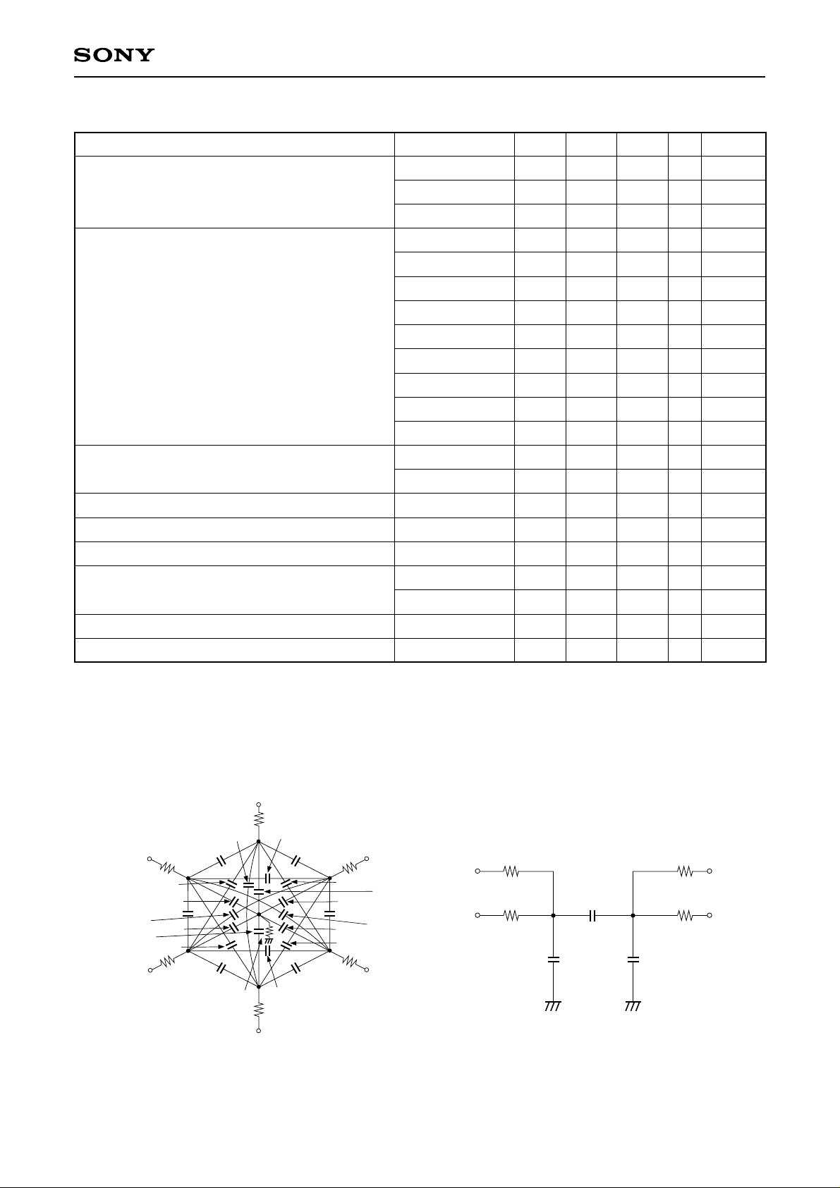
Clock Equivalent Circuit Constant
ICX282AKF
Item Min.
Capacitance between vertical transfer clock
and GND
Capacitance between vertical transfer clocks
Capacitance between horizontal transfer clock
and GND
Capacitance between horizontal transfer clocks
Capacitance between reset gate clock and GND
Capacitance between substrate clock and GND
Vertical transfer clock series resistor
Vertical transfer clock ground resistor
Horizontal transfer clock series resistor
Symbol
CφV1γ, CφV3γ
CφV1B, CφV3B
CφV2, CφV4
CφV1γ2, CφV3γ4
CφV1B2, CφV3B4
CφV23γ, CφV41γ
CφV23B, CφV41B
CφV1γ3γ
CφV1B3B
CφV1γ3B, CφV1B3γ
CφV24
CφV1γ1B, CφV3γ3B
CφH1
CφH2
CφHH
CφRG
CφSUB
R1γ, R3γ
R1B, R2, R3B, R4
RGND
RφH
Typ. Max.
1800
6800
5600
560
680
180
270
56
330
91
120
100
82
62
110
5
1500
62
43
16
7.5
Unit
pF
pF
pF
pF
pF
pF
pF
pF
pF
pF
pF
pF
pF
pF
pF
pF
pF
Ω
Ω
Ω
Ω
Remarks
Note 1) γ = A, C for each vertical transfer clock capacitance.
Note 2) The relationships of V1A = V1C and V3A = V3C are established for each vertical transfer clock
capacitance.
Note 3) CφV1A1C and CφV3A3C are sufficiently small relative to other capacitance between vertical transfer
clocks, and are also below the measurement limit, so these are omitted from the equivalent circuit
diagrams and the above table.
Vφ
2
R
2
Cφ
V1γ3
V1B3B
4
Cφ
Cφ
V23
V3B4
γ
γ
Vφ3γ (γ
3
γ
Cφ
CφV3γ
CφV3γ
Cφ
CφV3γ
R
3B
V23B
V3B
Vφ
3B
CφV1γ
4
3B
= A, C)
Cφ
V2
Rφ
Rφ
H
Hφ
1A
Rφ
H
Hφ
3B
1B
Cφ
H1
Cφ
HH
Cφ
H
Hφ
Rφ
H
Hφ
H2
R
Horizontal transfer clock equivalent circuit
Cφ
V24
Vφ1γ (γ
Cφ
V1B3
Cφ
= A, C)
Cφ
Cφ
γ
V4
Vφ
V1B2
CφV1γ
V1γ1B
Cφ
Cφ
1B
R1γ
V41
V1B
R
Cφ
V1γ2
γ
1B
Cφ
V41B
Cφ
R
GND
R
Vφ
4
Vertical transfer clock equivalent circuit
– 5 –
2A
2B
Drive Clock Waveform Conditions
(1) Readout clock waveform
100%
90%
V
VT
10%
0%
tr tf
twh
(2) Vertical transfer clock waveform
Vφ1A, Vφ1B, Vφ1C Vφ3A, Vφ3B, Vφ3C
ICX282AKF
φM
φM
2
0V
VVH1
VVL
Vφ2 Vφ4
VVHL
VVH2
VVHH
VVHH
VVLL
VVL1
VVHH
VVH
VVHL
VVLH
VVHH
VVHL
VVL3
VVH
VVHL
VVHL
VVHH
VVH
VVH3
VVHL
VVL
VVHL
VVHH
VVH4
VVHH
VVH
VVLH
VVLL
VVHH
VVHL
VVLL
VVL
VVH = (VVH1 + VVH2)/2
VVL = (VVL3 + VVL4)/2
VφV = VVHn – VVLn (n = 1 to 4)
VVL2
VVLH
– 6 –
VVL4
VVLH
VVLL
VVL
(3) Horizontal transfer clock waveform
ICX282AKF
twh tftr
Hφ2A, Hφ
2B
90%
V
CR
Vφ
Hφ1A, Hφ
10%
1B
H
two
Vφ
H
2
twl
HL
V
Cross-point voltage for the Hφ1 rising side of the horizontal transfer clocks Hφ1 and Hφ2 waveforms is VCR.
The overlap period for twh and twl of horizontal transfer clocks Hφ1 and Hφ2 is two.
(4) Reset gate clock waveform
RG waveform
tr twh
Vφ
RG
tf
V
RGH
twl
Point A
V
V
V
RGLH
RGLL
RGLm
V
RGL
VRGLH is the maximum value and VRGLL is the minimum value of the coupling wavefo rm during the period from
Point A in the above diagram until the rising edge of RG.
In addition, VRGL is the average value of VRGLH and VRGLL.
VRGL = (VRGLH + VRGLL)/2
Assuming VRGH is the minimum value during the interval with twh, then:
VφRG = VRGH – VRGL
Negative overshoot level during the falling edge of RG is VRGLm.
(5) Substrate clock waveform
100%
90%
φM
10%
V
(A bias generated within the CCD)
SUB
0%
VφSUB
tr tftwh
φM
2
– 7 –
Clock Switching Characteristics (Horizontal drive frequency: 22.5MHz)
ICX282AKF
Item
Readout clock
Vertical transfer
clock
Horizontal
transfer clock
Reset gate
clock
Substrate clock
Horizontal
transfer clock
Symbol
VT
Vφ1A, Vφ1B,
Vφ1C, Vφ2,
Vφ3A, Vφ3B,
Vφ3C, Vφ4
Hφ1A, Hφ1B
Hφ2A, Hφ2B
φRG
φSUB
Symbol
Hφ1A, Hφ1B,
Hφ2A, Hφ2B
twh
Min.
Typ. Max. Min. Typ. Max.Min. Typ. Max. Min. Typ. Max.
2.47
2.67
twl tr tf
0.5
15
13
13
6
2.0
16
16
8
2.58
131316
16
31
6.5
6.5
3
9.5
9.5
0.5
two
Min.
Typ. Max.
UnitnsRemarksItem
11 16
0.5
6.5
6.5
3
350
9.5
9.5
0.5
Unit
µs
ns
ns
ns
µs
Remarks
During
readout
When using
CXD3400N
During
imaging,
tf ≥ tr – 2ns
During drain
charge
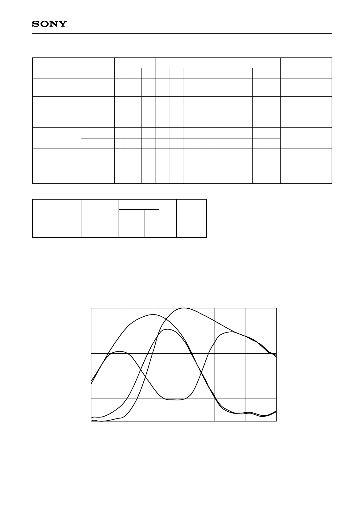
Spectral Sensitivity Characteristics (excludes lens characteristics and light source characteristics)
1.0
Ye
Cy
0.8
G
0.6
0.4
Relative Response
0.2
Mg
0
400 450 500 550
Wave Length [nm]
600 650 700
– 8 –
ICX282AKF
Image Sensor Characteristics (Ta = 25°C)
Item
Sensitivity
Sensitivity
comparison
Symbol
S
RMgG
RYeCy
Vsat
Min.
264
0.75
1.10
450
Typ.
330
Max.
1.35
1.43
Saturation signal
Smear
Video signal shading
Vsat2
Sm
SH
900
–92
–86
–80
–84
–78
–72
20
25
Dark signal
Dark signal shading
Lag
1
∗
Frame readout mode, 2× speed mode (1), and center scan modes (1), (2), (3) and (4).
2
∗
When the accumulation time is constant, 2-line addition modes have a sensitivity double that of modes
Vdt
∆Vdt
Lag
16
8
0.5
Measurement
Unit
method
mV
mV
dB
%
mV
mV
%
1
1/30s accumulation,
no line addition
2
No line addition
3
Ta = 60°C
2-line addition
Frame readout mode
4
2× speed mode (1)
8× speed mode
Zone 0 and I
5
Zone 0 to II'
6
7
Ta = 60°C, 3.75 frame/s
Ta = 60°C, 3.75 frame/s,
8
Remarks
1, ∗2
∗
4
∗
5
∗
without line addition.
3
∗
2× speed mode (2), 8× speed mode, and AF mode (1), (2)
4
∗
After closing the mechanical shutter, the smear can be reduced to below the detection limit by performing
vertical register sweep operation. This is also the same for 2× speed mode (2) and center scan modes (3)
and (4).
5
∗
Smear can be reduced by approximately 30dB to a level of approximately –116dB (typ.) by performing the
following sequence.
1
∗
3
∗
6
∗
Vertical register high-speed transfer → Readout (SG) → Mechanical shutter closed → Signal output
6
∗
Excludes vertical dark signal shading caused by vertical register high-speed transfer.
Zone Definition of Video Signal Shading
4
H
8
2588 (H)
V
10
V
10
4
Zone 0, I
Zone II, II'
Ignored region
Effective pixel region
H
8
8
1960 (V)
8
– 9 –
Measurement System
CCD signal output [∗A]
ICX282AKF
CCD C.D.S
Note) Adjust the amplifier gain so that the gain between [∗A] and [∗B], and between [∗A] and [∗C] equals 1.
AMP
S/H
S/H
G/Ye channel signal output [∗B]
Mg/Cy channel signal output [∗C]
Image Sensor Characteristics Measurement Method
Measurement conditions
(1) In the following measurements, the device drive conditions are at the typical values of the bias and clock
voltage conditions, and the frame readout mode is used.
(2) In the following measurements, spot blemishes are excluded and, unless otherwise specified, the optical
black level (OB) is used as the reference for the signal output, which is taken as the value of the Y signal
output or chroma signal output of the measurement system.
Color coding of this image sensor & Composition of luminance (Y) and chroma (color difference) signals
The complementary color filters of this image sensor are
B2
Ye Cy Ye Cy
GMgGMg
A2
arranged in the layout shown in the figure on the left.
For frame readout, the A1 and A2 lines are output as signals in
the A field, and the B1 and B2 lines in the B field.
B1
Ye Cy Ye Cy
GMgGMg
A1
Horizontal register
Color Coding Diagram
These signals are processed to form the Y signal and chroma (color difference) signal sa follws.
The approximation:
Y ={G + Mg + Ye + Cy} × 1/4
= 1/4 {2B + 3G +2R}
is used for the Y signal, and the approximation:
R – Y = {(Mg + Ye) – (G +Cy}
= {2R –G}
B – Y = {(Mg + Cy) – (G +Ye)}
= {2B –G}
are used for the chroma (color difference) signal.
– 10 –
ICX282AKF
Readout modes list
The readout method, frame rate, number of output lines and other information for each readout mode are
shown in the table below.
Mode
Frame
readout
2× speed (1)
2× speed (2)
8× speed
Center scan
(1)
Center scan
(2)
Center scan
(3)
Center scan
(4)
AF (1)
AF (2)
Readout
method
Frame
readout
2/4 lines
Frame
readout
4/16 lines
2/4 lines
2/4 lines
Frame
readout
Frame
readout
4/16 lines
4/16 lines
High-speed
sweep for
preventing smear
Yes
Yes
Yes
None
None
None
Yes
Yes
None
None
Addition
method
None
None
Vertical
2 lines
Vertical
2 lines
None
None
None
None
Vertical
2 lines
Vertical
2 lines
Frame rate [frame/s]
NTSC
3.75
7.49
6.66
29.97
14.985
PAL
3.57
7.14
6.25
25
12.5
26.35
7.02
11.988
59.94
119.88
10
50
100
Number of output
effective image data
lines
1960
980
980
245
NTSC: 484, PAL: 587
246
968
NTSC: 492, PAL: 620
NTSC: 104, PAL: 128
NTSC: 34, P AL: 46
– 11 –
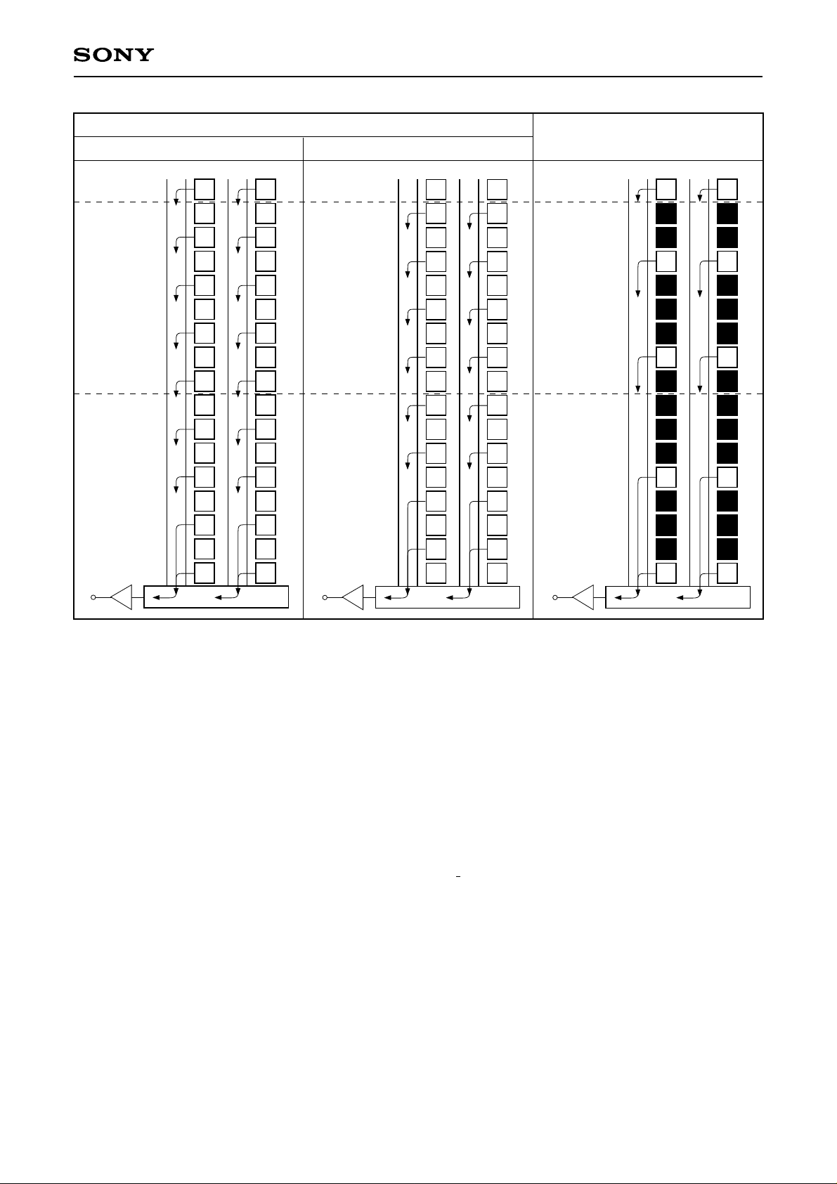
Description of frame readout mode
The output methods for the following readout modes are shown below.
ICX282AKF
V
OUT
16 (V3B)
15 (V1B)
14 (V3A)
13 (V1C)
12 (V3B)
11 (V1B)
10 (V3A)
9 (V1C)
8 (V3B)
7 (V1B)
6 (V3C)
5 (V1A)
4 (V3B)
3 (V1B)
2 (V3C)
1 (V1A)
Frame readout mode
1st field 2nd field
G17 (V1A)
Ye
G
Ye
G
Ye
G
Ye
G
Ye
G
Ye
G
Ye
G
Ye
G
Mg
Cy
Mg
Cy
Mg
Cy
Mg
Cy
Mg
Cy
Mg
Cy
Mg
Cy
Mg
Cy
Mg
V
OUT
16 (V3B)
15 (V1B)
14 (V3A)
13 (V1C)
12 (V3B)
11 (V1B)
10 (V3A)
9 (V1C)
8 (V3B)
7 (V1B)
6 (V3C)
5 (V1A)
4 (V3B)
3 (V1B)
2 (V3C)
1 (V1A)
G17 (V1A)
Ye
G
Ye
G
Ye
G
Ye
G
Ye
G
Ye
G
Ye
G
Ye
G
Mg
Cy
Mg
Cy
Mg
Cy
Mg
Cy
Mg
Cy
Mg
Cy
Mg
Cy
Mg
Cy
Mg
2× speed mode (1)
2/4-line readout
16 (V3B)
15 (V1B)
14 (V3A)
13 (V1C)
12 (V3B)
11 (V1B)
10 (V3A)
9 (V1C)
8 (V3B)
7 (V1B)
6 (V3C)
5 (V1A)
4 (V3B)
3 (V1B)
2 (V3C)
1 (V1A)
V
OUT
Ye
Ye
Ye
Ye
Ye
Ye
Ye
Ye
G17 (V1A)
G
G
R
G
G
G
G
G
Mg
Cy
Mg
Cy
Mg
Cy
Mg
Cy
Mg
Cy
Mg
Cy
Mg
Cy
Mg
Cy
Mg
Note) Blacked out portions in the diagram indicate pixels which are not read out.
1. Frame readout mode
In this mode, all pixel signals are divided into two fields and output.
All pixel signals are read out independently, making this mode suitable for high resolution image capturing.
2. 2× speed mode (1) 2/4-line readout
All effective area signals are output in half the time of frame readout mode by reading out 2 lines for every 4
lines.
The number of output lines is halved, but all color signals can be output in a single field, so exposure
completed is read out (SG), making high-speed shutter operation possible.
However, note that the G/Mg and Ye/Cy line readout timings have a time difference of approximately 6.7µs
(150clk).
In addition, using high-speed sweep transfer and the mechanical shutter is recommended to suppress
smear.
Smear is reduced by approximately 30dB by performing the following sequence.
Vertical register high-speed transfer → Readout (SG) → Mechanical shutter closed → Signal output
– 12 –
ICX282AKF
V
OUT
16 (V3B)
15 (V1B)
14 (V3A)
13 (V1C)
12 (V3B)
11 (V1B)
10 (V3A)
9 (V1C)
8 (V3B)
7 (V1B)
6 (V3C)
5 (V1A)
4 (V3B)
3 (V1B)
2 (V3C)
1 (V1A)
2× speed mode (2) 2-line addition
1st field 2nd field
G17 (V1A)
Ye
G
Ye
G
Ye
G
Ye
G
Ye
G
Ye
G
Ye
G
Ye
G
Mg
Cy
Mg
Cy
Mg
Cy
Mg
Cy
Mg
Cy
Mg
Cy
Mg
Cy
Mg
Cy
Mg
V
OUT
16 (V3B)
15 (V1B)
14 (V3A)
13 (V1C)
12 (V3B)
11 (V1B)
10 (V3A)
9 (V1C)
8 (V3B)
7 (V1B)
6 (V3C)
5 (V1A)
4 (V3B)
3 (V1B)
2 (V3C)
1 (V1A)
G17 (V1A)
Ye
G
Ye
G
Ye
G
Ye
G
Ye
G
Ye
G
Ye
G
Ye
G
Mg
Cy
Mg
Cy
Mg
Cy
Mg
Cy
Mg
Cy
Mg
Cy
Mg
Cy
Mg
Cy
Mg
V
OUT
8× speed mode
4/16-line readout
16 (V3B)
15 (V1B)
14 (V3A)
13 (V1C)
12 (V3B)
11 (V1B)
10 (V3A)
9 (V1C)
8 (V3B)
7 (V1B)
6 (V3C)
5 (V1A)
4 (V3B)
3 (V1B)
2 (V3C)
1 (V1A)
Ye
Ye
Ye
Ye
Ye
Ye
Ye
Ye
G17 (V1A)
G
G
G
G
G
G
G
G
Mg
Cy
Mg
Cy
Mg
Cy
Mg
Cy
Mg
Cy
Mg
Cy
Mg
Cy
Mg
Cy
Mg
Note) Blacked out portions in the diagram indicate pixels which are not read out.
3. 2× speed mode (2) 2-line addition
In this mode, the G/Mg line is read out in the 1st field and the Ye/Cy line in the 2nd field, 2 lines are
transferred during the horizontal blanking period, and 2 lines are added in the horizontal register.
All pixel signals are divided into two fields and output in appro ximately half the time (slightly longer than half)
of frame readout mode.
At this time, the sensitivity (for 1/30s accumulation) and saturation signal level are double that during frame
readout mode, allowing high sensitivity imaging with a wide dynamic range.
4. 8× speed mode, 4/16-line readout
All effective area signals are output in 1/8 the time of frame readout mode by reading out 4 lines for every 16
lines, transferring 4 lines during the horizontal blanking period, and adding 2 lines in the horizontal register.
The number of output lines is 245 lines.
However, note that the G/Mg and Ye/Cy line readout timings have a time difference of approximately 6.7µs
(150clk).
This mode emphasizes processing speed over vertical resolution, making it suitable for AE/AF and other
control and for image verification on LCD viewfinders.
– 13 –
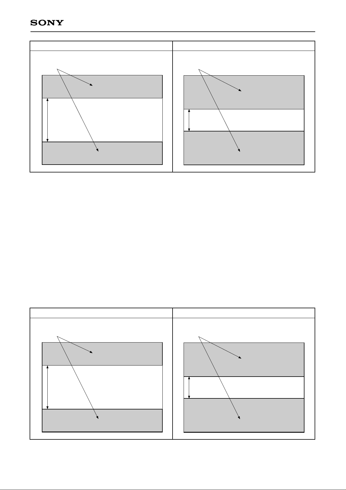
Center scan mode (1) 484-line output Center scan mode (2) 246-line output
ICX282AKF
Undesired portion
(Swept by vertical register high-speed transfer)
V: 968 pixels
Picture center cut-out portion
Undesired portion
(Swept by vertical register high-speed transfer)
V: 492 pixels
Picture center cut-out portion
5. Center scan mode (1) 484-line output
This mode sweeps the undesired portions by vertical register high-speed transfer, and outputs only the vertical
968-pixel region of the picture center by reading out 2 lines for every 4 lines (like 2× speed mode (1)).
The number of output lines is 484 lines.
The frame rate is increased (approximately 15 frames/s) by setting the number of vertical output lines to that
of VGA mode, making this mode suitable for VGA moving pictures. (However, the angle of view is equivalent
to 2× electronic zoom.)
6. Center scan mode (2) 246-line output
This mode sweeps the undesired portions by vertical register high-speed transfer, and outputs only the vertical
492-pixel region of the picture center by reading out 2 lines for every 4 lines (like 2× speed mode (1)).
The number of output lines is 246 lines.
This mode is suitable for enlarged display when verifying image on LCD viewfinders.
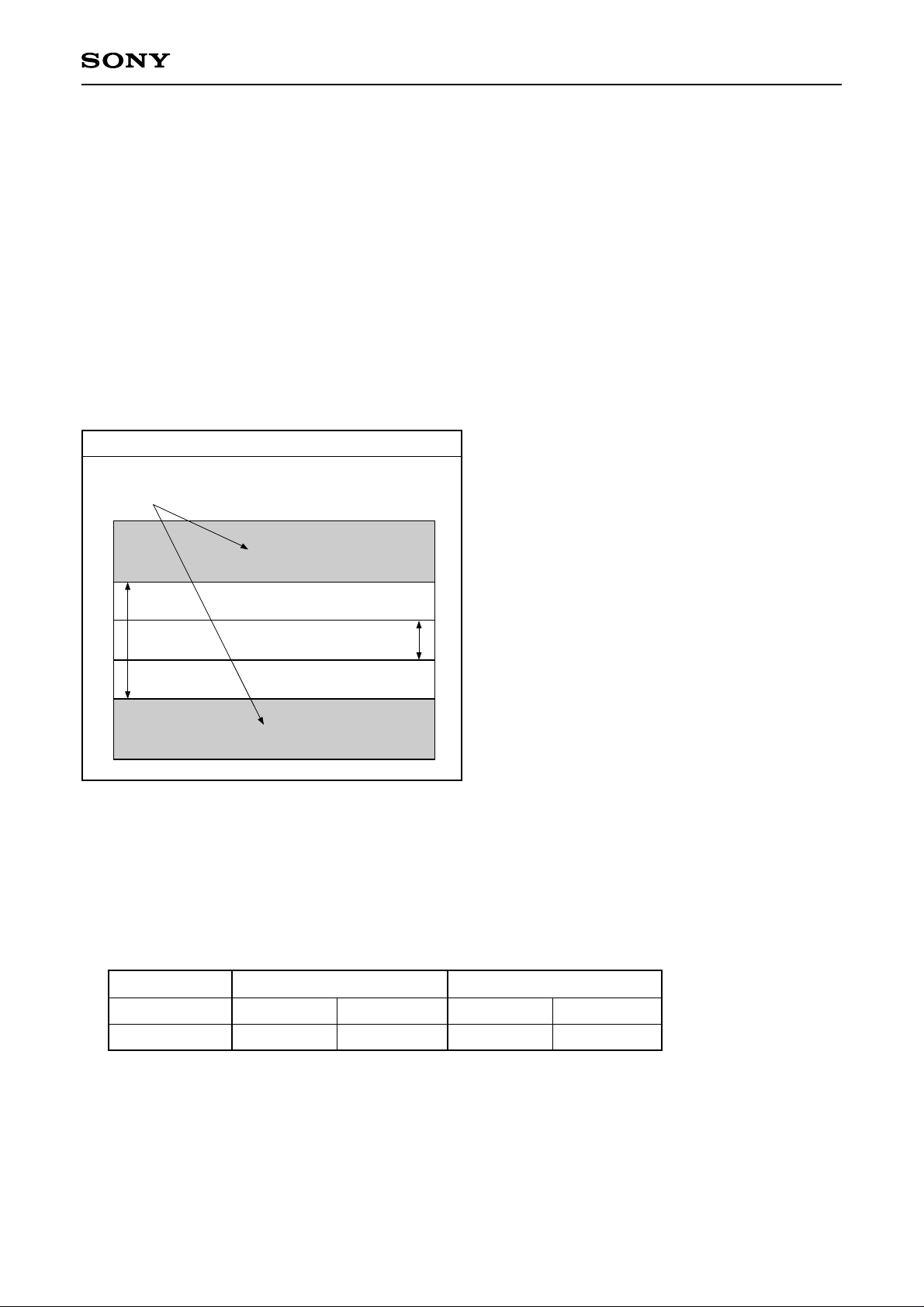
Center scan mode (3) 968-line output Center scan mode (4) 492-line output
Undesired portion
(Swept by vertical register high-speed transfer)
V: 968 pixels
Picture center cut-out portion
Undesired portion
(Swept by vertical register high-speed transfer)
V: 492 pixels
Picture center cut-out portion
– 14 –
ICX282AKF
7. Center scan mode (3) 968-line output
This mode sweeps the undesired portions by vertical register high-speed transfer, and outputs only the
vertical 968-pixel region of the the picture center divided into two fields (like frame readout mode).
The number of output lines is 968 lines.
This mode is used to shorten the frame rate when shooting 2× electronic zoom image.
8. Center scan mode (4) 492-line output
This mode sweeps the undesired portions by vertical register high-speed transfer, and outputs only the
vertical 492-pixel region of the picture center divided into two fields (like frame readout mode).
The number of output lines is 492 lines.
This mode is used to shorten the frame rate when shooting 4× electronic zoom image.
AF mode (1), (2)
Undesired portion
(Swept by vertical register high-speed transfer)
Picture center cut-out portion
AF mode (2)
V: 272 pixels
AF mode (1)
V: 832 pixels
9. AF modes (1), (2)
The AF modes are used to achieve even higher-speed AF control than 8× speed mode.
AF mode (1) outputs only the vertical 832-pixel (in NTSC mode) region of the picture center at
approximately 60 frames/s by reading out 4 lines for every 16 lines (like 8× speed mode).
AF mode (2) outputs only the vertical 272-pixel (in NTSC mode) region of the picture center at
approximately 120 frames/s by reading out 4 lines for every 16 lines (like 8× speed mode).
The number of output lines for each mode is shown below.
AF mode (1) AF mode (2)
NTSC mode
PAL mode
60 frame/s
50 frame/s
104 lines
128 lines
120 frame/s
100 frame/s
34 lines
46 lines
– 15 –
 Loading...