

Sony ICX278AK Datasheet
ICX278AK
Diagonal 4.5mm (Type 1/4) CCD Image Sensor for NTSC Color Video Cameras
Description
The ICX278AK is an interline CCD solid-state
image sensor suitable for NTSC color video cameras
with a diagonal 4.5mm (Type 1/4) system. Compared
with the current product ICX208AK, basic
characteristics such as sensitivity, smear and
dynamic range are improved drastically through the
adoption of EXview HAD CCDTM technology.
This chip features a field period readout system and
an electronic shutter with variable charge-storage time.
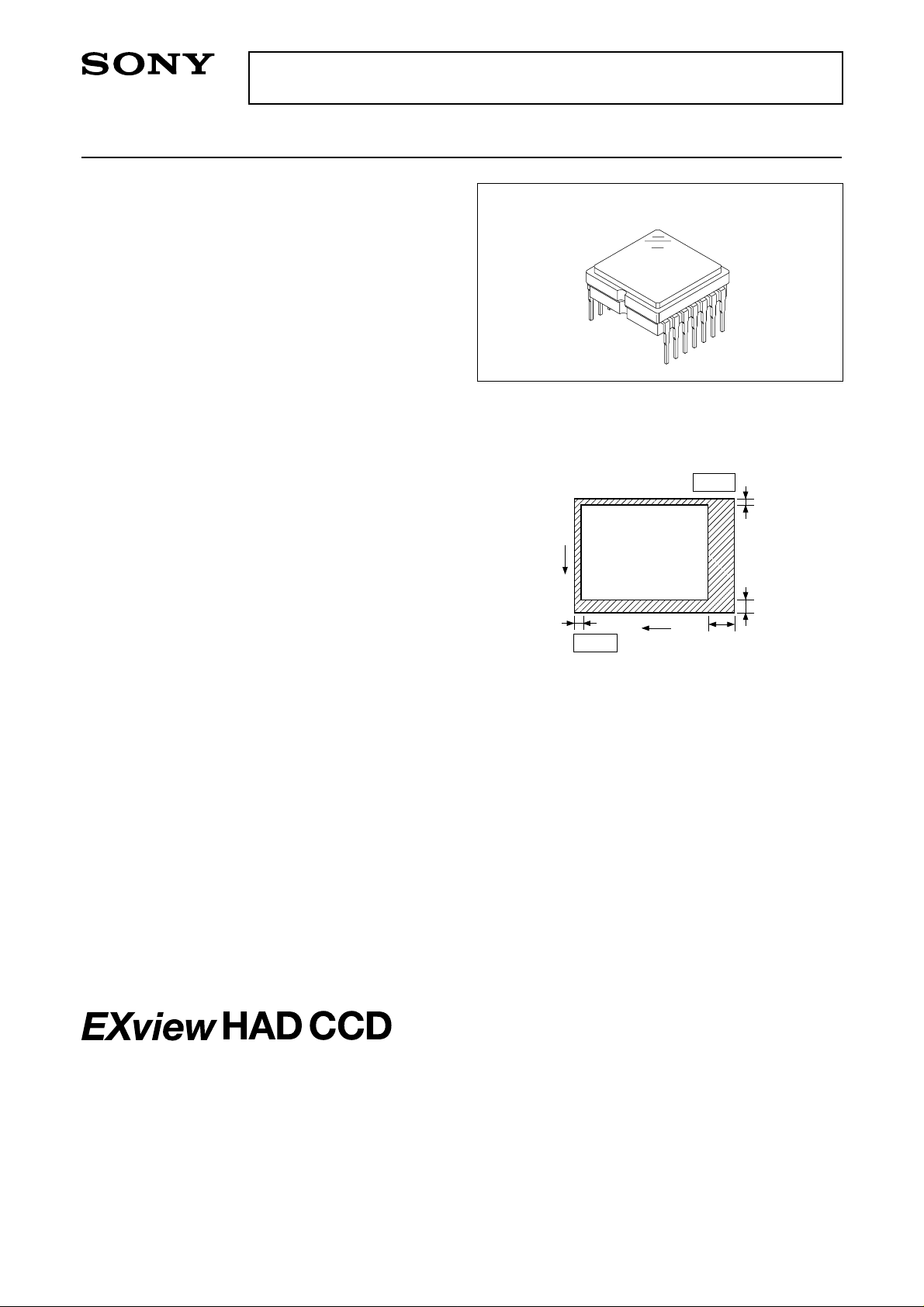
The package is a 10mm-square 14-pin DIP (Plastic).
EXview HAD CCDTM has different spectral
characteristics from the current CCD.
14 pin DIP (Plastic)
Features
• High sensitivity (+5dB compared with the ICX208AK)
• Low smear (–20dB compared with the ICX208AK)
• High D range (+2dB compared with the ICX208AK)
• Horizontal register: 3.3 to 5.0V drive
V
• Reset gate: 3.3 to 5.0V drive
• No voltage adjustment
(Reset gate and substrate bias are not adjusted.)
• High resolution, low smear and low dark current
• Excellent antiblooming characteristics
• Continuous variable-speed shutter
• Recommended range of exit pupil distance: –20 to –100mm
• Ye, Cy, Mg, and G complementar y color mosaic filters on chip
3
Pin 8
Optical black position
(T op View)
Device Structure
• Interline CCD image sensor
• Image size: Diagonal 4.5mm (Type 1/4)
• Number of effective pixels: 768 (H) × 494 (V) approx. 380K pixels
• Total number of pixels: 811 (H) × 508 (V) approx. 410K pixels
• Chip size: 4.43mm (H) ×3.69mm (V)
• Unit cell size: 4.75µm (H) × 5.55µm (V)
• Optical black: Horizontal (H) direction: Front 3 pixels, rear 40 pixels
Vertical (V) direction: Front 12 pixels, rear 2 pixels
• Number of dummy bits: Horizontal 22
Vertical 1 (even fields only)
• Substrate material: Silicon
Pin 1
2
12
H
40
TM
∗
EXview HAD CCD is a trademark of Sony Corporation.
EXview HAD CCD is a CCD that drastically improves light efficiency by including near infrared light region as a basic structure of
HAD (Hole-Accumulation-Diode) sensor.
Sony reserves the right to change products and specifications without prior notice. This information does not convey any license by
any implication or otherwise under any patents or other right. Application circuits shown, if any, are typical examples illustrating the
operation of the devices. Sony cannot assume responsibility for any problems arising out of the use of these circuits.
– 1 –
E00Z49-PS
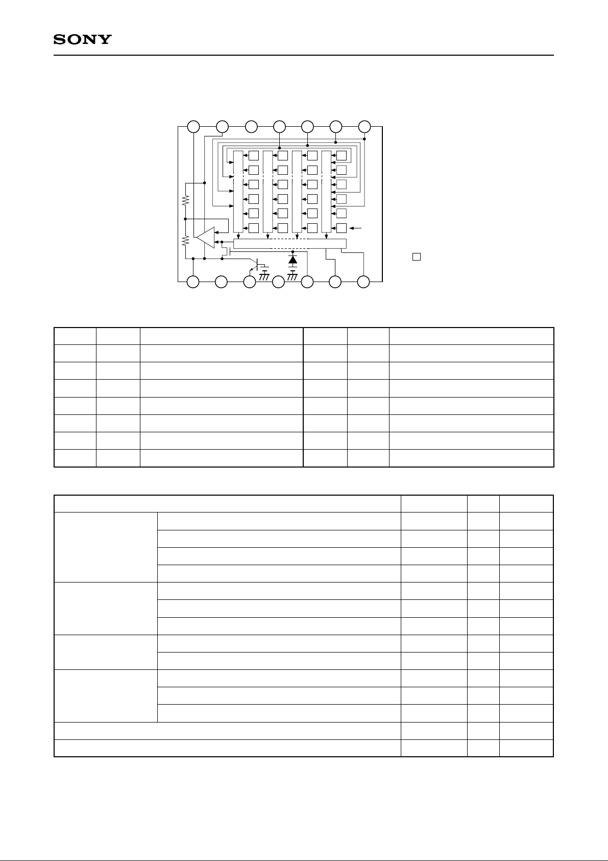
Block Diagram and Pin Configuration
(Top View)
OUT
V
GND
7 6 5 4 3 2 1
NC
ICX278AK
1
2
3
Vφ
Vφ
4
Vφ
Vφ
Pin Description
Cy
Mg
Cy
G
Cy
Vertical Register
Mg
Horizontal Register
8 9 10 11 12 13 14
DD
V
GND
φSUB
Cy
Ye
G
Ye
Mg
Ye
G
L
V
Mg
Cy
G
Cy
Mg
RG
Ye
G
Ye
Mg
Ye
G
Note)
Note) : Photo sensor
1
2
Hφ
Hφ
Pin No. Symbol Description Pin No. Symbol Description
1
Vφ4
2
Vφ3
3
Vφ2
4
Vφ1
5
NC
6
GND
Vertical register transfer clock
Vertical register transfer clock
Vertical register transfer clock
Vertical register transfer clock
GND
8
9
10
11
12
13
VDD
GND
φSUB
VL
RG
Hφ1
Supply voltage
GND
Substrate clock
Protective transistor bias
Reset gate clock
Horizontal register transfer clock
7
VOUT
Signal output
14
Absolute Maximum Ratings
Item
VDD, VOUT, RG – φSUB
Vφ1, Vφ3 – φSUB
Against φSUB
Vφ2, Vφ4, VL – φSUB
Hφ1, Hφ2, GND – φSUB
VDD, VOUT, RG – GND
Against GND
Vφ1, Vφ2, Vφ3, Vφ4 – GND
Hφ1, Hφ2 – GND
Vφ1, Vφ3 – VL
Against VL
Vφ2, Vφ4, Hφ1, Hφ2, GND – VL
Voltage difference between vertical clock input pins
Between input clock
pins
Hφ1 – Hφ2
Hφ1, Hφ2 – Vφ4
Storage temperature
Operating temperature
1
∗
+24V (Max.) when clock width < 10µs, clock duty factor < 0.1%.
– 2 –
Hφ2
Horizontal register transfer clock
Ratings Unit Remarks
–40 to +8
–50 to +15
–50 to +0.3
–40 to +0.3
–0.3 to +18
–10 to +18
–10 to +6
–0.3 to +28
–0.3 to +15
to +15
–5 to +5
–13 to +13
–30 to +80
–10 to +60
V
V
V
V
V
V
V
V
V
V
V
V
°C
°C
1
∗
Bias Conditions
ICX278AK
Item
Supply voltage
Protective transistor bias
Substrate clock
Reset gate clock
1
∗
VL setting is the VVL voltage of the vertical transfer clock waveform, or the same power supply as the VL
Symbol
VDD
VL
φSUB
φRG
Min.
14.55 15.45
15.0
1
∗
2
∗
2
∗
Unit RemarksTyp. Max.
V
power supply for the V dr iver should be used.
2
∗
Do not apply a DC bias to the substrate clock and reset gate clock pins, because a DC bias is generated
within the CCD.
DC Characteristics
Item
Supply current
Symbol4Min. Unit RemarksTyp. Max.
IDD
mA6
Clock V olta ge Conditions
V
V
Waveform
diagram
1
2
Remarks
VVH = (VVH1 + VVH2)/2
Item
Readout clock voltage
Symbol
VVT
VVH1, VVH2
Min.
14.55
–0.05
Typ.
15.0
0
Max. Unit
15.45
0.05
Vertical transfer clock
voltage
Horizontal transfer
clock voltage
Reset gate clock
voltage
Substrate clock voltage
VVH3, VVH4
VVL1, VVL2,
VVL3, VVL4
VφV
VVH3 – VVH
VVH4 – VVH
VVHH
VVHL
VVLH
VVLL
VφH
VHL
VφRG
VRGLH – VRGLL
VRGL – VRGLm
VφSUB
–0.2
–8.0
6.3
–0.25
–0.25
3.0
–0.05
3.0
21.0
0
–7.0
7.0
3.3
0
3.3
22.0
0.05
–6.5
8.05
0.1
0.1
0.3
0.3
0.3
0.3
5.25
0.05
5.5
0.4
0.5
23.5
V
V
V
V
V
V
V
V
V
V
V
V
V
V
V
2
2
VVL = (VVL3 + VVL4)/2
2
VφV = VVHn – VVLn (n = 1 to 4)
2
2
2
High-level coupling
2
High-level coupling
2
Low-level coupling
2
Low-level coupling
3
3
Input through 0.1µF
4
capacitance
4
Low-level coupling
4
Low-level coupling
5
– 3 –
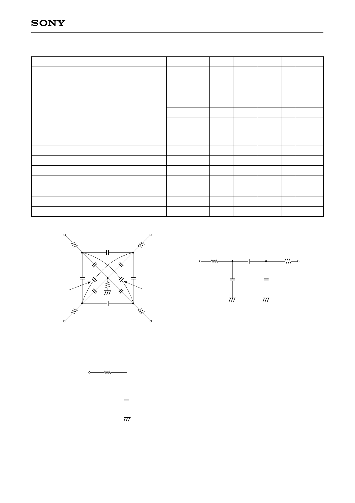
Clock Equivalent Circuit Constant
ICX278AK
Item Min.
Capacitance between vertical transfer clock
and GND
Capacitance between vertical transfer clocks
Capacitance between horizontal transfer clock
and GND
Capacitance between horizontal transfer clocks
Capacitance between reset gate clock and GND
Capacitance between substrate clock and GND
Vertical transfer clock series resistor
Vertical transfer clock ground resistor
Horizontal transfer clock series resistor
Reset gate clock series resistor
Vφ
Vφ
1
2
Symbol
CφV1, CφV3
CφV2, CφV4
CφV12, CφV34
CφV23, CφV41
CφV13
CφV24
CφH1, CφH2
CφHH
CφRG
CφSUB
R1, R2, R3, R4
RGND
RφH
RφRG
Typ. Max.
1200
560
220
120
82
75
22
36
5
180
82
15
12
51
Unit Remarks
pF
pF
pF
pF
pF
pF
pF
pF
pF
pF
Ω
Ω
Ω
Ω
Cφ
Vφ
Cφ
V24
4
Cφ
Cφ
V12
V1
V4
R
Cφ
GND
V34
Cφ
Cφ
V2
V3
Cφ
Cφ
R
R
V23
V13
3
2
Vφ
Rφ
H
Hφ
1
Cφ
H1
3
Cφ
HH
Cφ
Rφ
H
Hφ
2
H2
R
1
Cφ
V41
R
4
Horizontal transfer clock equivalent circuitVertical transfer clock equivalent circuit
Rφ
RGφ
RG
Cφ
RG
Reset gate clock equivalent circuit
– 4 –
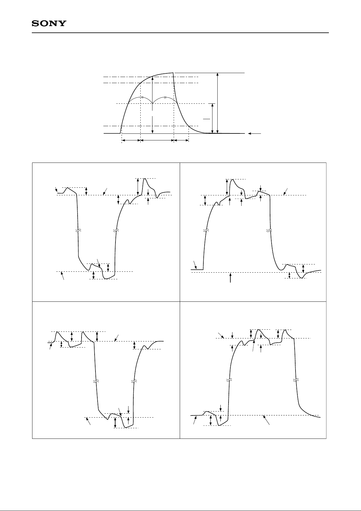
Drive Clock Waveform Conditions
(1) Readout clock waveform
100%
90%
V
VT
10%
0%
tr tf
twh
(2) Vertical transfer clock waveform
Vφ1 Vφ3
ICX278AK
φM
φM
2
0V
VVH1
VVL
Vφ2 Vφ4
VVHL
VVH2
VVHH
VVHH
VVLL
VVL1
VVHH
VVH
VVHL
VVLH
VVHH
VVHL
VVL3
VVH
VVHL
VVHL
VVHH
VVH
VVH3
VVHL
VVL
VVHL
VVHH
VVH4
VVHH
VVH
VVLH
VVLL
VVHH
VVHL
VVLL
VVL
VVH = (VVH1 + VVH2)/2
VVL = (VVL3 + VVL4)/2
VφV = VVHn – VVLn (n = 1 to 4)
VVL2
VVLH
– 5 –
VVL4
VVLH
VVLL
VVL
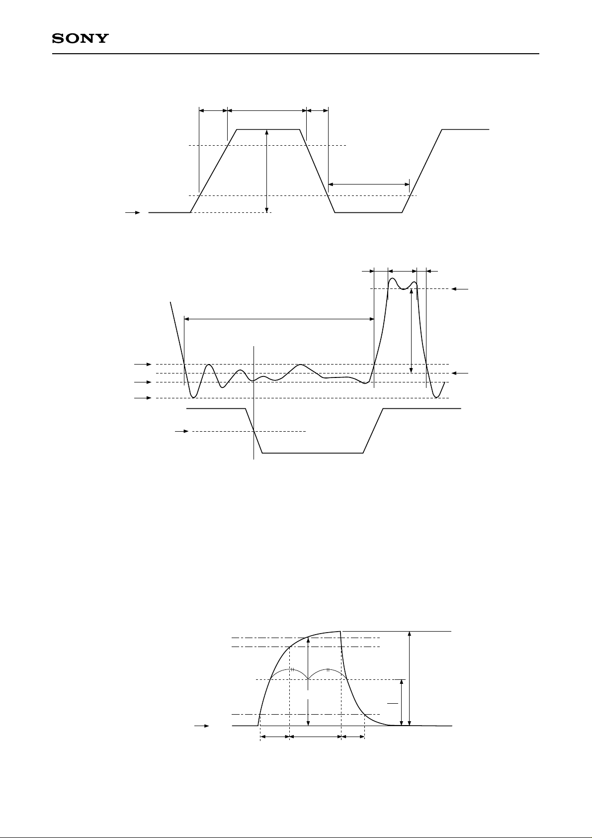
(3) Horizontal transfer clock waveform
tr twh tf
90%
10%
V
HL
Vφ
ICX278AK
H
twl
(4) Reset gate clock waveform
twhtr tf
VRGH
twl
RG
Vφ
VRGL
RG waveform
VRGLH
V
RGLL
VRGLm
Hφ1 waveform
H/2 [V]
Vφ
Point A
VRGLH is the maximum value and VRGLL is the minimum value of the coupling waveform during the period from
Point A in the above diagram until the rising edge of RG. In addition, VRGL is the average value of VRGLH and
VRGLL.
VRGL = (VRGLH + VRGLL)/2
Assuming VRGH is the minimum value during the interval twh, then:
VφRG = VRGH – VRGL
Negative overshoot level during the falling edge of RG is VRGLm.
(5) Substrate clock waveform
V
(A bias generated within the CCD)
SUB
100%
90%
10%
0%
Vφ
SUB
tr tftwh
– 6 –
φM
φM
2
 Loading...