

Sony ICX274AQ User Manual
ICX274A Q
Diagonal 8.923mm (Type 1/1.8) Progressive Scan CCD Image Sensor with Square Pixel for Color Cameras
Description
The ICX274AQ is a diagonal 8.923mm (Type 1/1.8)
interline CCD solid-state image sensor with a square
pixel array and 2.01M effective pixels. Progressive
scan allows all pixels' signals to be output
independently within approximately 1/15 second,
and output is also possible using various addition
and pulse elimination methods. This chip features an
electronic shutter with variable charge-storage time
which makes it possible to realize full-frame still
images without a mechanical shutter. High resolution
and high color reproductivity are achieved through
the use of R, G, B primary color mosaic filters as the
color filters. Further, high sensitivity and low dark
current are achieved through the adoption of Super
HAD CCD technology.
This chip is suitable for applications such as
electronic still cameras, PC input cameras, etc.
Features
• High horizontal and vertical resolution
• Supports the following modes
Progressive scan mode (with/without mechanical shutter)
2/8-line readout mode
2/4-line readout mode
2-line addition mode
Center scan modes (1), (2) and (3)
AF modes (1) and (2)
• Square pixel
• Horizontal drive frequency: 28.6364MHz (typ.), 36.0MHz (max.)
• Reset gate bias are not adjusted
• R, G, B primary color mosaic filters on chip
• High sensitivity, low dark current
• Continuous variable-speed shutter function
• Excellent anti-blooming characteristics
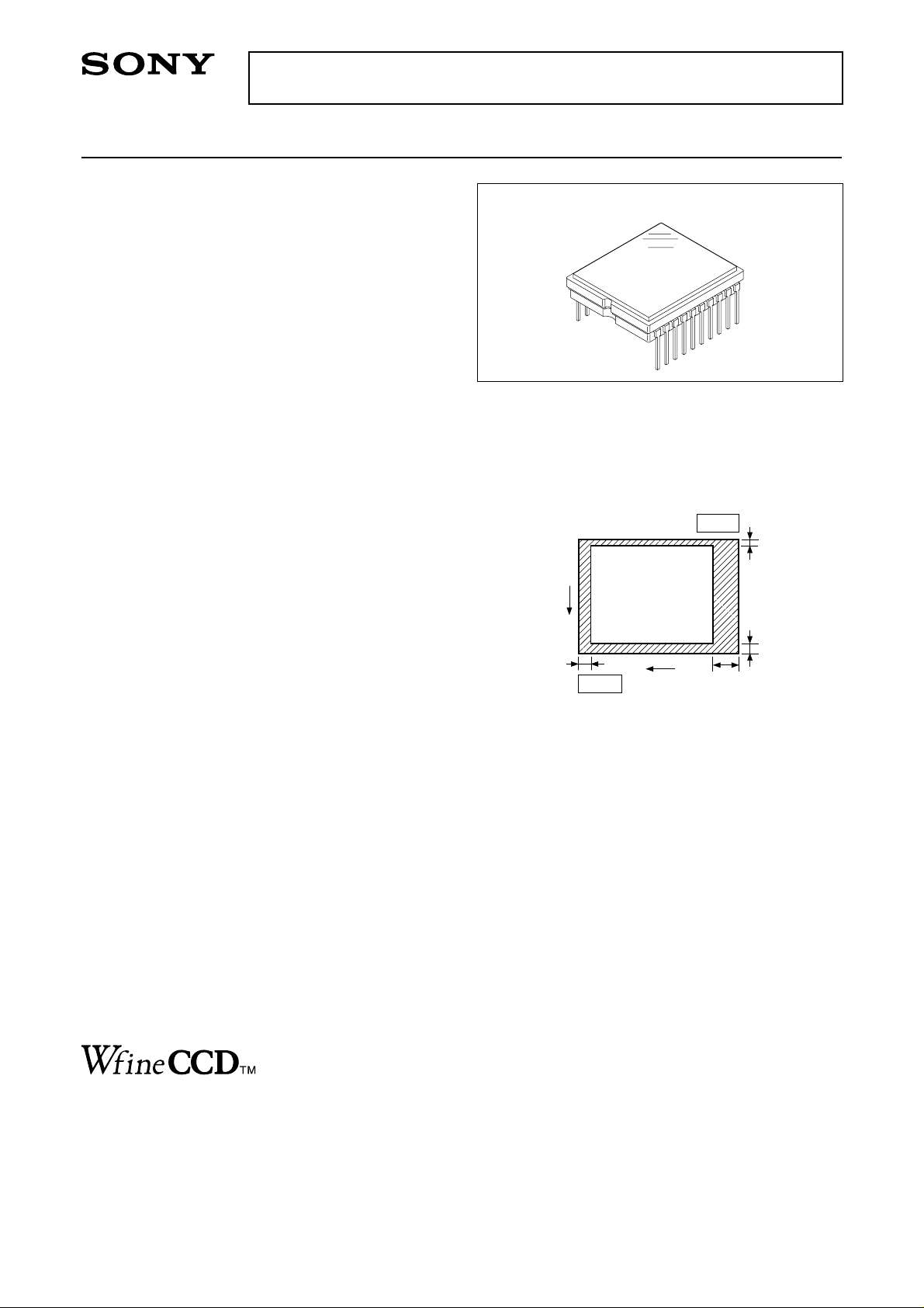
• 20-pin high-precision plastic package
20 pin DIP (Plastic)
V
12
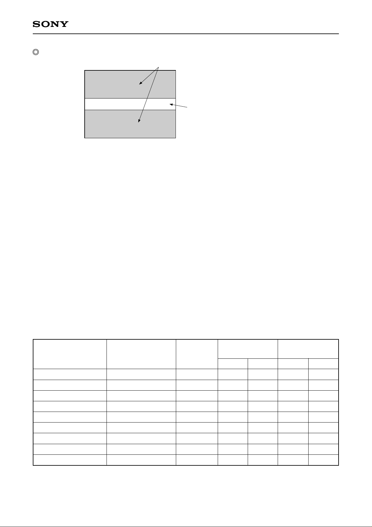
Pin 11
Optical black position
H
(T op View)
Pin 1
2
10
48
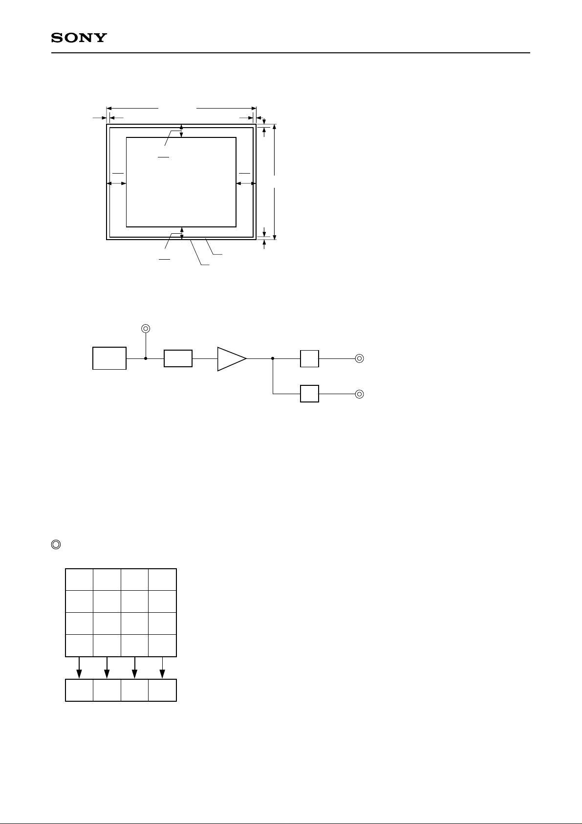
Device Structure
• Interline CCD image sensor
• Image size: Diagonal 8.923mm (Type 1/1.8)
• Total number of pixels: 1688 (H) × 1248 (V) approx. 2.11M pixels
• Number of effective pixels: 1628 (H) × 1236 (V) approx. 2.01M pixels
• Number of active pixels: 1620 (H) × 1220 (V) approx. 1.98M pixels
• Recommended number of
recording pixels: 1600 (H) × 1200 (V) approx. 1.92M pixels
• Chip size: 8.50mm (H) × 6.80mm (V)
• Unit cell size: 4.40µm (H) × 4.40µm (V)
• Optical black: Horizontal (H) direction: Front 12 pixels, rear 48 pixels
Vertical (V) direction: Front 10 pixels, rear 2 pixels
• Number of dummy bits: Horizontal 28
Vertical 1
• Substrate material: Silicon
∗
Wfine CCD is trademark of Sony corporation.
Represents a CCD adopting progressive scan, primary color filter and square pixel.
Sony reserves the right to change products and specifications without prior notice. This information does not convey any license by
any implication or otherwise under any patents or other right. Application circuits shown, if any, are typical examples illustrating the
operation of the devices. Sony cannot assume responsibility for any problems arising out of the use of these circuits.
– 1 –
E01410B23-PS
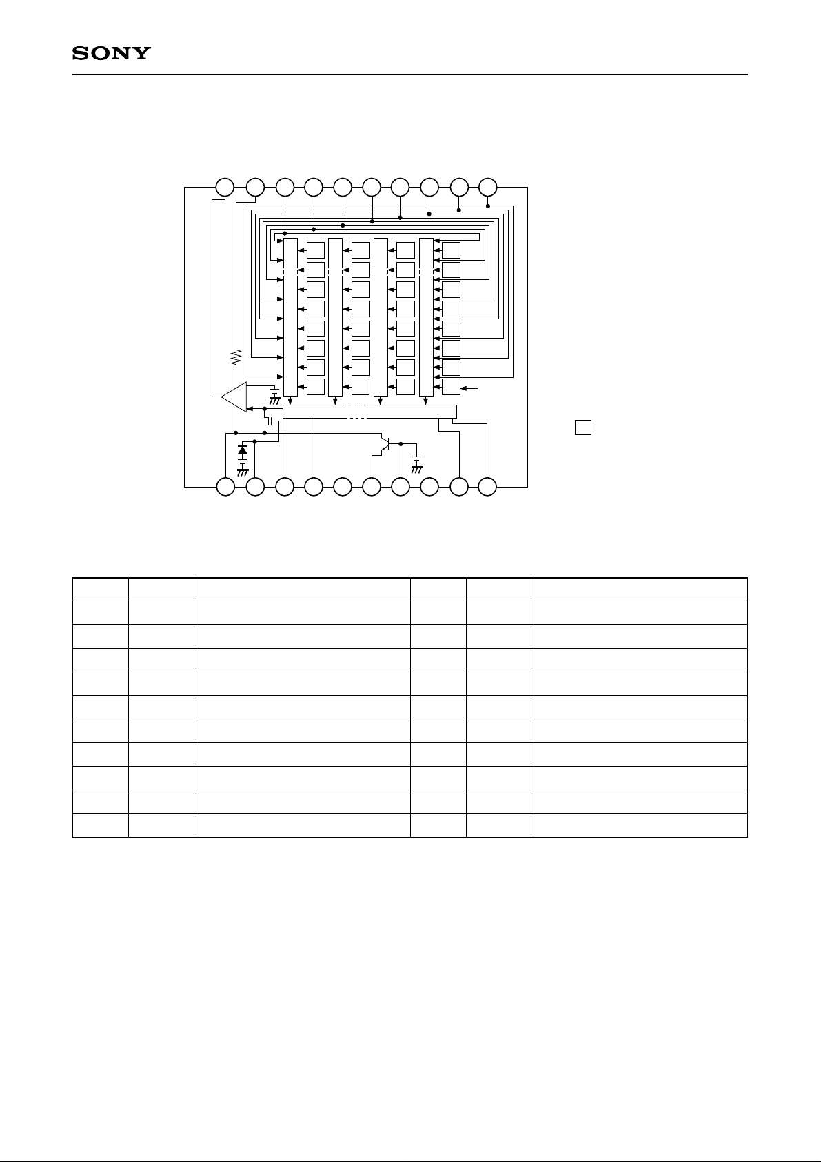
Block Diagram and Pin Configuration
(Top View)
OUT
V
GND
Vφ1Vφ2CVφ2BVφ2AVφ3CVφ3BVφ3AVφ
10 9 8 7 6 5 4 3 2 1
ICX274AQ
4
B
G
B
G
B
G
B
GRGR
Note)
Note) : Photo sensor
L
V
2A
Hφ1AHφ
φSUB
G
R
G
R
G
R
G
SUB
C
G
R
G
R
G
R
Vertical register
G
11 12 13 14 15 16 17 18 19 20
φRG
2BHφ1B
Hφ
DD
V
B
G
B
G
B
G
B
Horizontal register
GND
Pin Description
Pin No. Symbol Description Pin No. Symbol Description
1
Vφ4
2
Vφ3A
Vertical register transfer clock
Vertical register transfer clock
11
12
VDD
φRG
Supply voltage
Reset gate clock
3
Vφ3B
4
Vφ3C
5
Vφ2A
6
Vφ2B
7
Vφ2C
8
Vφ1
9
GND
10
1
∗
DC bias is generated within the CCD, so that this pin should be grounded externally through a capacitance of
VOUT
Vertical register transfer clock
Vertical register transfer clock
Vertical register transfer clock
Vertical register transfer clock
Vertical register transfer clock
Vertical register transfer clock
GND
Signal output
13
14
15
16
17
18
19
20
Hφ2B
Hφ1B
GND
φSUB
CSUB
VL
Hφ1A
Hφ2A
Horizontal register transfer clock
Horizontal register transfer clock
GND
Substrate clock
1
Substrate bias
∗
Protective transistor bias
Horizontal register transfer clock
Horizontal register transfer clock
0.1µF.
– 2 –
Absolute Maximum Ratings
ICX274AQ
Item
DD, VOUT, φRG – φSUB
V
Vφ
2α, Vφ3α – φSUB (α = A to C)
Against φSUB
Vφ1, Vφ4, VL – φSUB
Hφ1β, Hφ2β, GND – φSUB (β = A, B)
CSUB – φSUB
VDD, VOUT, φRG, CSUB – GND
Against GND
Vφ1, Vφ2α, Vφ3α, Vφ4 – GND (α = A to C)
Hφ1β, Hφ2β – GND (β = A, B)
Vφ2α, Vφ3α – VL (α = A to C)
Against VL
Vφ1, Vφ4, Hφ1β, Hφ2β, GND – VL (β = A, B)
Voltage difference between vertical clock input pins
Between input
clock pins
Hφ1β – Hφ2β (β = A, B)
Hφ1β, Hφ2β – Vφ4 (β = A, B)
Storage temperature
Guaranteed temperature of performance
Operating temperature
Ratings Unit Remarks
–40 to +12
–50 to +15
–50 to +0.3
–40 to +0.3
–25 to
–0.3 to +22
–10 to +18
–10 to +6.5
–0.3 to +28
–0.3 to +15
to +15
–6.5 to +6.5
–10 to +16
–30 to +80
–10 to +60
–10 to +75
V
V
V
V
V
V
V
V
V
V
V
V
V
°C
°C
°C
2
∗
2
∗
+24V (Max.) is guaranteed when clock width < 10µs, clock duty factor < 0.1%.
+16V (Max.) is guaranteed during power-on or power-off.
– 3 –
Bias Conditions
ICX274AQ
Item
Supply voltage
Protective transistor bias
Substrate voltage
adjustment range
No line addition
2-line addition
∗
Substrate voltage adjustment accuracy
Reset gate clock
1
∗
Progressive scan mode, 2/8-line readout mode, 2/4-line readout mode, center scan modes (1) and (3),
Symbol
VDD
VL
1
∗
VSUB
2
VSUB2
∆VSUB
φRG
Min.
14.55
Internally generated value
8.8
Indicated
voltage – 0.2
15.0
3
∗
Indicated
voltage
5
∗
15.45
14.4
Indicated
voltage + 0.2
Unit
V
V
V
V
and AF modes (1) and (2)
2
∗
2-line addition mode and center scan mode (2)
3
∗
VL setting is the VVL voltage of the vertical clock waveform, or the same voltage as the VL power supply
for the V driver should be used.
4
∗
Substrate voltage (VSUB2) setting value indication
The substrate voltage (VSUB) for modes without line addition is generated internally.
The substrate voltage setting value for use with vertical 2-line addition is indicated by a code on the
bottom surface of the image sensor. Adjust the substrate voltage to the indicated voltage.
VSUB2 code – 1-digit indication
↑
VSUB2 code
RemarksTyp. Max.
4
∗
The code and the actual value correspond as follows.
VSUB2 code
Actual value
VSUB2 code
Actual value
1
8.829.039.249.469.679.8810.0910.2A10.4C10.6d10.8E11.0f11.2G11.4h11.6
J
11.8K12.0L12.2m12.4N12.6P12.8R13.0S13.2U13.4V13.6W13.8X14.0Y14.2Z14.4
[Example] "h" indicates a VSUB2 setting of 11.6V.
5
∗
Do not apply a DC bias to the reset gate clock pin, because a DC bias is generated within the CCD.
DC characteristics
Item
Supply current
Symbol
IDD
Min. Unit RemarksTyp. Max.
10.0
mA13.07.0
– 4 –
Clock V olta ge Conditions
ICX274AQ
Item
Readout clock
voltage
Vertical transfer
clock voltage
Horizontal transfer
clock voltage
Symbol
V
VT
VVH1, VVH2
VVH3, VVH4
VVL1, VVL2,
VVL3, VVL4
VφV
VVH3 – VVH
VVH4 – VVH
VVHH
VVHL
VVLH
VVLL
VφH
VHL
VCR
Min.
14.55
–0.05
–0.2
–8.0
6.8
–0.25
–0.25
4.75
–0.05
0.8
Typ.
15.0
0
0
–7.5
7.5
5.0
0
2.5
Max. Unit
15.45
0.05
0.05
–7.0
8.05
0.1
0.1
0.5
0.5
0.5
0.5
5.25
0.05
V
V
V
V
V
V
V
V
V
V
V
V
V
V
Waveform
diagram
1
2
2
2
2
2
2
2
2
2
2
3
3
3
Remarks
VVH = (VVH1 + VVH2)/2
VVL = (VVL3 + VVL4)/2
VφV = VVHn – VVLn (n = 1 to 4)
High-level coupling
High-level coupling
Low-level coupling
Low-level coupling
Cross-point voltage
Reset gate clock
voltage
Substrate clock
voltage
VφRG
VRGLH – VRGLL
VRGL – VRGLm
VφSUB
3.0
21.5
3.3
22.5
5.25
0.4
0.5
23.5
5
4
4
Low-level coupling
4
Low-level coupling
V
V
V
V
– 5 –
Clock Equivalent Circuit Constants
ICX274AQ
Item Min.
Capacitance between vertical transfer clock and
GND
Capacitance between vertical transfer clocks
Symbol
CφV1
CφV2A, CφV2B
CφV2C
CφV3A, CφV3B
CφV3C
CφV4
CφV12 (A, B)
CφV12C
CφV13 (A, B)
CφV13C
CφV14
CφV2 (A, B), 3 (A, B)
CφV2 (A, B), 3C
CφV2 (A, B), 4
CφV2C, 3 (A, B)
CφV2C, 3C
Typ. Max.
3300
1200
2700
1000
1800
6800
120
220
150
270
2700
470
680
680
1000
820
Unit Remarks
pF
pF
pF
pF
pF
pF
pF
pF
pF
pF
pF
pF
pF
pF
pF
pF
Capacitance between horizontal transfer clock
and GND
Capacitance between horizontal transfer clocks
Capacitance between reset gate clock and GND
Capacitance between substrate clock and GND
CφV2C, 4
CφV3 (A, B), 4
CφV3C, 4
CφH1
CφH2
CφHH
CφRG
CφSUB
R1, R4
1800
820
1500
100
100
47
2
820
30
pF
pF
pF
pF
pF
pF
pF
pF
Ω
Vertical transfer clock series resistor
Vertical transfer clock ground resistor
Horizontal transfer clock series resistor
Horizontal transfer clock ground resistor
Reset gate clock and series resistor
R2 (A, B, C), 3 (A, B, C)
RGND
RφH
RφH2
RφRG
62
15
7
20
4.7
Ω
Ω
Ω
kΩ
Ω
Note 1) Expressions using parentheses such as CφV2 (A,B), 3C indicate items which include all combinations of
the pins within the parentheses.
For example, CφV2 (A, B), 3C indicates [CφV2A3C, CφV2B3C].
– 6 –
Vφ
Cφ
4
Cφ
V2α4 (α = A to C)
R
4
Cφ
V4
Cφ
V3α4 (α = A to C)
Cφ
V13α (α = A to C)
V14
Cφ
V1
Vφ
Vφ
1
R
1
R
Cφ
R
3α (α = A to C)
3α (α = A to C)
Cφ
V12α (α = A to C)
GND
Cφ
Cφ
V2α3α (α = A to C)
V3α (α = A to C)
R
2α (α = A to C)
V2α (α = A to C)
Vφ
2α (α = A to C)
ICX274AQ
Rφ
H
Hφ
Rφ
H
Hφ
Rφ
H2
H2
Hφ
Hφ
Rφ
H
1A
Rφ
H
1B
Cφ
H1
Cφ
HH
Cφ
Horizontal transfer clock equivalent circuit
Rφ
RGφ
RG
2A
2B
Note 2) Cφ2α2β and Cφ3α3β (α = A to C, β = A to C other than α) are
sufficiently small relative to other capacitance between
other vertical clocks in the equivalent circuit, so these
are omitted from the equivalent circuit diagram.
Cφ
RG
Reset gate clock equivalent circuitVertical transfer clock equivalent circuit
– 7 –
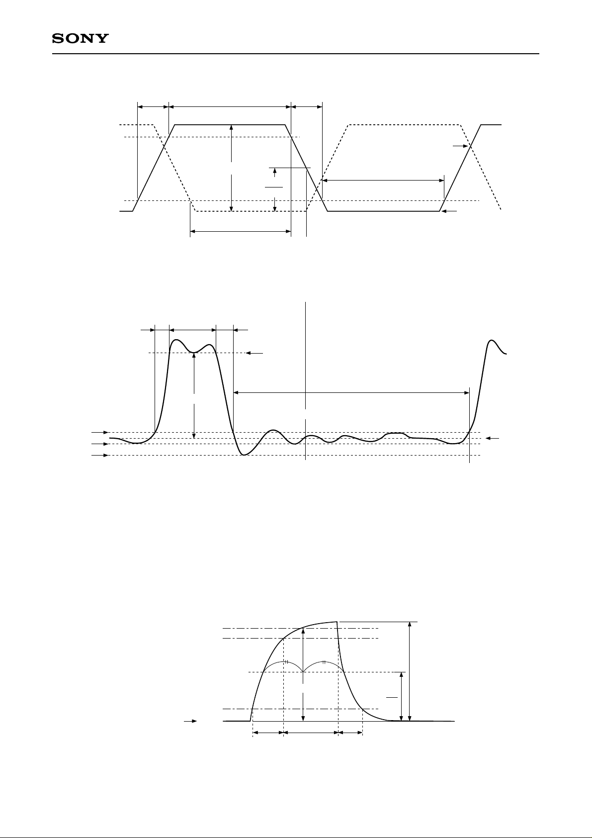
Drive Clock Waveform Conditions
(1) Readout clock waveform
100%
90%
V
VT
10%
0%
tr tf
twh
(2) Vertical transfer clock waveform
Vφ1 Vφ3A, Vφ3B, Vφ3C
V
VH1
V
VHH
V
VH
V
VHH
φM
ICX274AQ
φM
2
0V
V
V
VHH
VHH
V
VH
V
VHL
V
VHL
V
VL1
V
VLH
V
VLL
V
VL
V
Vφ2A, Vφ2B, Vφ2C Vφ4
V
VHH
V
VHL
V
VH2
V
VHH
V
VH
V
VHL
VL3
V
VHL
V
V
VH
V
VHL
V
VH3
VL
V
VHL
V
VLH
V
VLL
V
V
VHH
V
VH4
VHH
V
VHL
V
V
VL
VVH = (VVH1 + VVH2)/2
VVL = (VVL3 + VVL4)/2
VφV = VVHn – VVLn (n = 1 to 4)
VLL
V
V
VLH
V
VL2
V
VL4
VLH
V
VLL
V
VL
– 8 –
ICX274AQ
(3) Horizontal transfer clock waveform
tf
VCR
twl
VHL
Hφ
Hφ
2β
90%
10%
1β
tr
twh
Vφ
H
VφH
2
two
Cross-point voltage for the Hφ1β rising side of the horizontal transfer clocks Hφ1β and Hφ2β waveforms is VCR.
The overlap period for twh and twl of horizontal transfer clocks Hφ1β and Hφ2β is two. (β = A, B)
(4) Reset gate clock waveform
RG waveform
V
RGLH
V
RGLL
V
RGLm
tr twh
Vφ
RG
tf
V
RGH
twl
Point A
V
RGL
VRGLH is the maximum value and VRGLL is the minimum value of the coupling waveform during the period from
Point A in the above diagram until the rising edge of RG.
In addition, VRGL is the average value of VRGLH and VRGLL.
VRGL = (VRGLH + VRGLL)/2
Assuming VRGH is the minimum value during the interval twh, then:
VφRG = VRGH – VRGL
Negative overshoot level during the falling edge of RG is VRGLm.
(5) Substrate clock waveform
100%
90%
10%
V
(Internally generated bias)
SUB
0%
Vφ
SUB
tr tftwh
– 9 –
φM
φM
2
Clock Switching Characteristics (Horizontal drive frequency: 28.6364MHz)
ICX274AQ
Item
Readout clock
Vertical transfer
clock
Horizontal
transfer clock
Reset gate clock
Substrate clock
Horizontal
transfer clock
Symbol
VT
Vφ1, Vφ4,
Vφ2α, Vφ3α
(α = A to C)
Hφ1β (β = A, B)
Hφ2β (β = A, B)
φRG
φSUB
Symbol
Hφ1A, Hφ1B,
Hφ2A, Hφ2B
twh
Min.
Typ. Max.Min. Typ.Max.Min. Typ.Max. Min. Typ.Max.
3.3
3.5
twl tr tf
0.5
15
10
10
4
12.5
12.5
7
2.1
101012.5
12.5
24
5
7.5
5
7.5
2
0.5
two
UnitnsRemarksItem
Min.
Typ. Max.
810
0.5
5
5
3
400
7.5
7.5
0.5
Unit
During
µs
readout
∗
ns
∗
ns
ns
During drain
µs
charge
Remarks
1
2
Clock Switching Characteristics (Horizontal drive frequency: 36MHz)
Item
Readout clock
Vertical transfer
clock
Horizontal
transfer clock
Reset gate clock
Substrate clock
Symbol
VT
Vφ1, Vφ4,
Vφ2α, Vφ3α
(α = A to C)
Hφ1β (β = A, B)
Hφ2β (β = A, B)
φRG
φSUB
twh
Min.
Typ. Max.Min. Typ.Max.Min. Typ.Max. Min. Typ.Max.
4.0
4.2
8
9
8
9
4
5.5
1.67
twl tr tf
0.5
889
9
8
5
5
2
two
UnitnsRemarksItem
Horizontal
transfer clock
Symbol
Hφ1A, Hφ1B,
Hφ2A, Hφ2B
Min.
Typ. Max.
89
6
6
0.25
15
0.5
5
5
3
400
6
6
0.25
Unit
During
µs
readout
∗
ns
∗
ns
ns
During drain
µs
charge
Remarks
1
2
1
∗
When two vertical transfer clock drivers CXD3400N are used.
2
∗
tf ≥ tr – 2ns, and the cross-point voltage (VCR) for the Hφ1β (β = A, B) rising side of the Hφ1β and H φ2β
waveforms must be VφH/2 [V] or more.
– 10 –
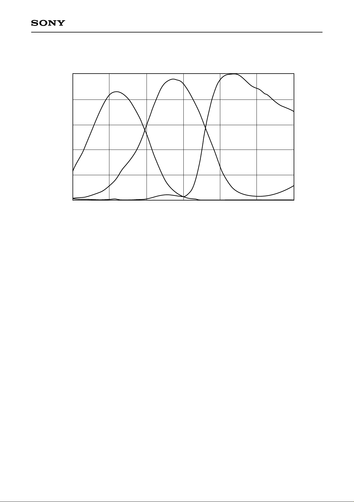
Spectral Sensitivity Characteristics (excludes lens characteristics and light source characteristics)
1.0
BG R
0.8
0.6
0.4
Relative Response
0.2
ICX274AQ
0
400 450 500 550
Wave Length [nm]
600 650 700
– 11 –
ICX274AQ
Image Sensor Characteristics (Ta = 25°C)
Item
G Sensitivity
Sensitivity
comparison
R
B
Saturation signal
Smear
Video signal shading
Uniformity between
video signal channels
Dark signal
Dark signal shading
Line crawl G
Line crawl R
Line crawl B
Lag
Symbol
Sg
Rr
Rb
Vsat
Vsat2
Sm
SH
∆Srg
∆Sbg
Vdt
∆Vdt
Lcg
Lcr
Lcb
Lag
Min.
335
0.35
0.45
Typ.
420
0.5
0.6
Max.
545
0.65
0.75
400
1
∗
400
–100
–94
–88
–92
–86
–80
20
25
8
Measurement
Unit
method
mV
mV
dB
%
%
Remarks
1
1/30s accumulation
1
1
2
2
Ta = 60°C
2-line addition
Progressive scan mode
No line addition
3
2/4-line readout mode
2/8-line readout mode
∗
3
∗
4
∗
5
∗
6
∗
Zone 0 and I
4
Zone 0 to II’
5
8
8
2
3.8
3.8
3.8
0.5
mV
mV
%
%
%
%
6
7
8
8
8
9
Ta = 60°C, 14.985 frame/s
Ta = 60°C, 14.985 frame/s,
7
∗
1
∗
Vsat2 is the saturation signal level in 2-line addition mode, and is 200mV per pixel.
2
∗
Progressive scan mode, 2/8-line readout mode, 2/4-line readout mode, and center scan modes (1) and (3).
3
∗
2-line addition mode and center scan mode (2).
4
∗
Same for 2-line addition mode and center scan modes (2) and (3).
5
∗
Same for center scan mode (1).
6
∗
Same for AF modes (1) and (2).
7
∗
Excludes vertical dark signal shading caused by vertical register high-speed transfer.
– 12 –
Zone Definition of Video Signal Shading
1628 (H)
4
V
H
8
10
ICX274AQ
4
8
H
8
1236 (V)
10
Zone 0, I
Zone II, II’
V
Ignored region
Effective pixel region
8
Measurement System
CCD signal output [∗A]
CCD C.D.S
AMP
S/H
S/H
Gr/Gb channel signal output [∗B]
R/B channel signal output [∗C]
Note) Adjust the amplifier gain so that the gain between [∗A] and [∗B], and between [∗A] and [∗C] equals 1.
Image Sensor Characteristics Measurement Method
Color coding of this image sensor & Readout
Gb B Gb B
The primary color filters of this image sensor are arranged in the layout
shown in the figure on the left (Bayer arrangement).
RGrRGr
Gb B Gb B
Gr and Gb denote the G signals on the same line as the R signal and the
B signal, respectively.
RGrRGr
Horizontal register
Color Coding Diagram
– 13 –
ICX274AQ
Readout modes
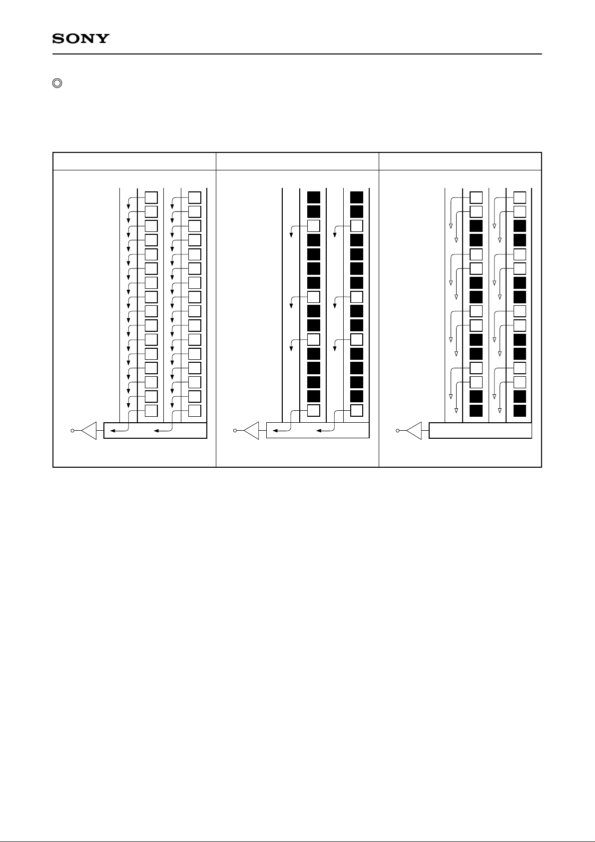
The diagrams below and on the following pages show the output methods for the following nine readout
modes.
2/4-line readout modeProgressive scan mode 2/8-line readout mode
16 (V2C/V3C)
15 (V2C/V3C)
14 (V2A/V3A)
13 (V2B/V3B)
12 (V2C/V3C)
11 (V2C/V3C)
10 (V2B/V3B)
9 (V2A/V3A)
8 (V2C/V3C)
7 (V2C/V3C)
6 (V2A/V3A)
5 (V2B/V3B)
4 (V2C/V3C)
3 (V2C/V3C)
2 (V2B/V3B)
1 (V2A/V3A)
OUT
V
G
R
G
R
G
R
G
R
G
R
G
R
G
R
G
R
B
G
B
G
B
G
B
G
B
G
B
G
B
G
B
G
16 (V2C/V3C)
15 (V2C/V3C)
14 (V2A/V3A)
13 (V2B/V3B)
12 (V2C/V3C)
11 (V2C/V3C)
10 (V2B/V3B)
9 (V2A/V3A)
8 (V2C/V3C)
7 (V2C/V3C)
6 (V2A/V3A)
5 (V2B/V3B)
4 (V2C/V3C)
3 (V2C/V3C)
2 (V2B/V3B)
1 (V2A/V3A)
OUT
V
G
R
G
R
G
R
G
R
G
R
G
R
G
R
G
R
B
G
B
G
B
G
B
G
B
G
B
G
B
G
B
G
16 (V2C/V3C)
15 (V2C/V3C)
14 (V2A/V3A)
13 (V2B/V3B)
12 (V2C/V3C)
11 (V2C/V3C)
10 (V2B/V3B)
9 (V2A/V3A)
8 (V2C/V3C)
7 (V2C/V3C)
6 (V2A/V3A)
5 (V2B/V3B)
4 (V2C/V3C)
3 (V2C/V3C)
2 (V2B/V3B)
1 (V2A/V3A)
OUT
V
Note) Blacked out portions in the diagram indicate pixels which are not read out.
Output starts from line 1 in 2/8-line decimation mode.
G
R
G
R
G
R
G
R
G
R
G
R
G
R
G
R
B
G
B
G
B
G
B
G
B
G
B
G
B
G
B
G
1. Progressive scan mode
In this mode, all pixel signals are output in non-interlace format in 1/14.985s.
All pixel signals within the same exposure period are read out simultaneously, making this mode suitable
for high resolution image capturing.
2. 2/8-line readout mode
All effective area signals are output in approximately 1/30s by reading out the signals for only two out of
eight lines (1st and 6th lines, 9th and 14th lines).
This readout mode emphasizes processing speed over vertical resolution, making it suitable for AE/AF and
other control and for checking images on LCD viewfinders.
3. 2/4-line readout mode
All effective area signals are output in approximately 1/20s by reading out the signals for only two out of
four lines (3rd and 4th lines, 7th and 8th lines, and so on).
– 14 –
ICX274AQ
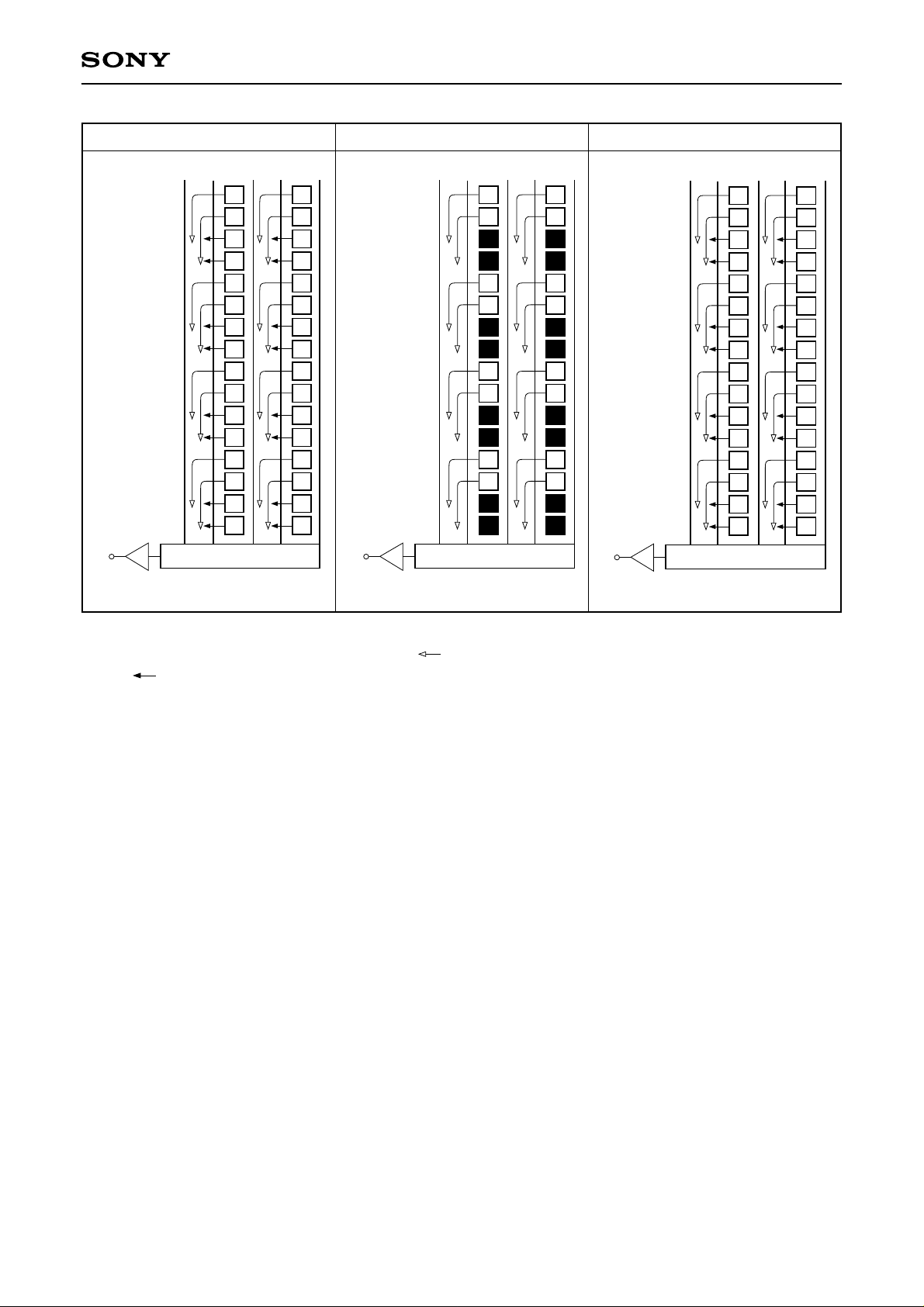
Center scan mode (2)2-line addition mode Center scan mode (1)
16 (V2C/V3C)
15 (V2C/V3C)
14 (V2A/V3A)
13 (V2B/V3B)
12 (V2C/V3C)
11 (V2C/V3C)
10 (V2B/V3B)
9 (V2A/V3A)
8 (V2C/V3C)
7 (V2C/V3C)
6 (V2A/V3A)
5 (V2B/V3B)
4 (V2C/V3C)
3 (V2C/V3C)
2 (V2B/V3B)
1 (V2A/V3A)
OUT
V
G
R
G
R
G
R
G
R
G
R
G
R
G
R
G
R
B
G
B
G
B
G
B
G
B
G
B
G
B
G
B
G
16 (V2C/V3C)
15 (V2C/V3C)
14 (V2A/V3A)
13 (V2B/V3B)
12 (V2C/V3C)
11 (V2C/V3C)
10 (V2B/V3B)
9 (V2A/V3A)
8 (V2C/V3C)
7 (V2C/V3C)
6 (V2A/V3A)
5 (V2B/V3B)
4 (V2C/V3C)
3 (V2C/V3C)
2 (V2B/V3B)
1 (V2A/V3A)
OUT
V
G
R
G
R
G
R
G
R
G
R
G
R
G
R
G
R
B
G
B
G
B
G
B
G
B
G
B
G
B
G
B
G
16 (V2C/V3C)
15 (V2C/V3C)
14 (V2A/V3A)
13 (V2B/V3B)
12 (V2C/V3C)
11 (V2C/V3C)
10 (V2B/V3B)
9 (V2A/V3A)
8 (V2C/V3C)
7 (V2C/V3C)
6 (V2A/V3A)
5 (V2B/V3B)
4 (V2C/V3C)
3 (V2C/V3C)
2 (V2B/V3B)
1 (V2A/V3A)
V
OUT
Note) Blacked out portions in the diagram indicate pixels which are not read out.
After reading out the pixels indicated by and transferring two lines, the pixels indicated by
are read out and two pixels of the same color are added by the vertical transfer block.
G
R
G
R
G
R
G
R
G
R
G
R
G
R
G
R
B
G
B
G
B
G
B
G
B
G
B
G
B
G
B
G
4. 2-line addition mode
In this mode, the signals for only two out of four lines (3rd and 4th lines, 7th and 8th lines, and so on) are
read out, the vertical register is shifted by 2 bits, and then the signals of the remaining two out of the four
lines (1st and 2nd lines, 5th and 6th lines, and so on) are read out and added within the vertical register. All
effective area signals are output in approximately 1/20s.
5. Center scan mode (1)
In this mode, the signals for only two out of four lines (3rd and 4th lines, 7th and 8th lines, and so on) are
read out. The undesired por tions are swept by vertical register high-speed transfer, and the vertical
1136-pixel region in the center of the picture is output by the above readout method. The number of
output lines is 568 lines at 36MHz, and 434 lines at 28.6364MHz. The frame rate is increased
(approximately 30 frames/s) by setting the number of output lines to that of VGA mode, making this
mode suitable for VGA moving pictures. (However, the angle of view decreases.)
6. Center scan mode (2)
In this mode, the signals for only two out of four lines (3rd and 4th lines, 7th and 8th lines, and so on) are
read out, the vertical register is shifted by 2 bits, and then the signals of the remaining two out of the four
lines (1st and 2nd lines, 5th and 6th lines, and so on) are read out and added within the vertical register.
The undesired portions are swept by vertical register high-speed transfer, and the vertical 1136-pixel region
in the center of the picture is output by the above readout method. The number of output lines is 568 lines
at 36MHz, and 434 lines at 28.6364MHz. The frame rate is increased (approximately 30 frames/s) by
setting the number of output lines to that of VGA mode, making this mode suitable for VGA moving pictures.
(However, the angle of view decreases.)
– 15 –
ICX274AQ
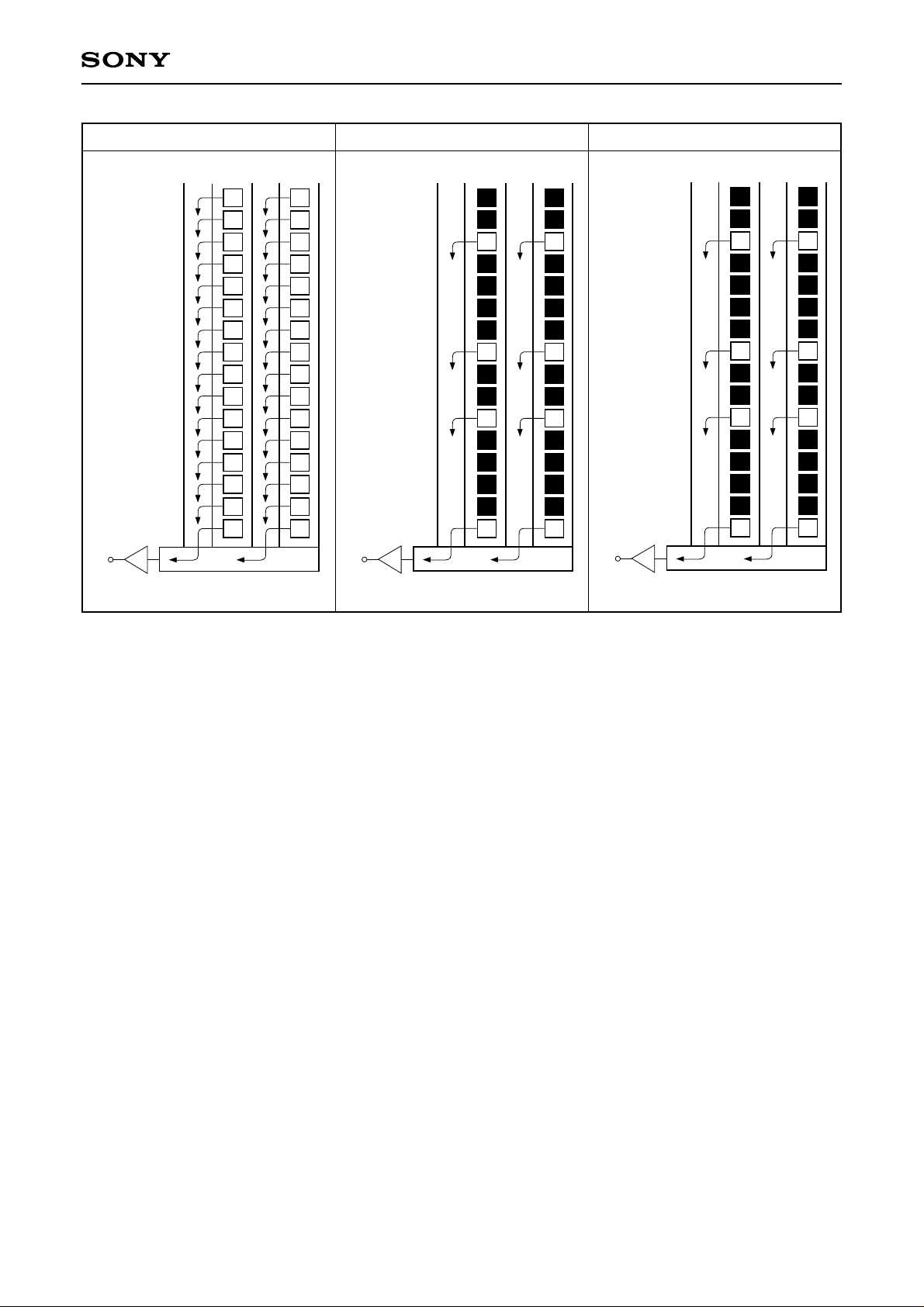
AF mode (2)Center scan mode (3) AF mode (1)
16 (V2C/V3C)
15 (V2C/V3C)
14 (V2A/V3A)
13 (V2B/V3B)
12 (V2C/V3C)
11 (V2C/V3C)
10 (V2B/V3B)
9 (V2A/V3A)
8 (V2C/V3C)
7 (V2C/V3C)
6 (V2A/V3A)
5 (V2B/V3B)
4 (V2C/V3C)
3 (V2C/V3C)
2 (V2B/V3B)
1 (V2A/V3A)
V
OUT
G
R
G
R
G
R
G
R
G
R
G
R
G
R
G
R
B
G
B
G
B
G
B
G
B
G
B
G
B
G
B
G
16 (V2C/V3C)
15 (V2C/V3C)
14 (V2A/V3A)
13 (V2B/V3B)
12 (V2C/V3C)
11 (V2C/V3C)
10 (V2B/V3B)
9 (V2A/V3A)
8 (V2C/V3C)
7 (V2C/V3C)
6 (V2A/V3A)
5 (V2B/V3B)
4 (V2C/V3C)
3 (V2C/V3C)
2 (V2B/V3B)
1 (V2A/V3A)
V
OUT
G
R
G
R
G
R
G
R
G
R
G
R
G
R
G
R
B
G
B
G
B
G
B
G
B
G
B
G
B
G
B
G
16 (V2C/V3C)
15 (V2C/V3C)
14 (V2A/V3A)
13 (V2B/V3B)
12 (V2C/V3C)
11 (V2C/V3C)
10 (V2B/V3B)
9 (V2A/V3A)
8 (V2C/V3C)
7 (V2C/V3C)
6 (V2A/V3A)
5 (V2B/V3B)
4 (V2C/V3C)
3 (V2C/V3C)
2 (V2B/V3B)
1 (V2A/V3A)
V
OUT
Note) Blacked out portions in the diagram indicate pixels which are not read out.
G
R
G
R
G
R
G
R
G
R
G
R
G
R
G
R
B
G
B
G
B
G
B
G
B
G
B
G
B
G
B
G
7. Center scan mode (3)
This is the center scan mode using the progressive scan method.
The undesired portions are swept by vertical register high-speed transfer, and the picture center is cut out.
The number of output lines is 580 lines at 36MHz, and 444 lines at 28.6364MHz.
8. AF mode (1)
In this mode, the undesired portions are swept by vertical register high-speed transfer, and the vertical
940-pixel region in the center of the picture is output in approximately 1/60s by reading out the signals for
only two out of eight lines (1st and 6th lines, 9th and 14th lines). The number of output lines is 235 lines at
36MHz, and 170 lines at 28.6364MHz. This mode aims for even faster AF control than 2/8-line readout
mode.
9. AF mode (2)
In this mode, the undesired portions are swept by vertical register high-speed transfer, and the vertical
300-pixel region in the center of the picture is output in approximately 1/120s by reading out the signals for
only two out of eight lines (1st and 6th lines, 9th and 14th lines). The number of output lines is 75 lines at
36MHz, and 43 lines at 28.6364MHz. This mode aims for even faster AF control than 2/8-line readout
mode.
– 16 –
ICX274AQ
Center scan and AF modes
Undesired portions (Swept by vertical register high-speed transfer)
Picture center cut-out portion
Description of Center Scan and AF Mode Operation
The center scan and AF modes realize high frame rates by sweeping the top and bottom of the picture with
high-speed transfer and cutting out the center of the picture.
The various readout modes during center scan and AF operation are described below.
• AF modes
AF mode (1), (2): The output method is the same as readout in 2/8-line readout mode.
• Center scan modes
Center scan mode (1): The output method is the same as 2/4-line readout mode.
Center scan mode (2): The output method consists of 2-line addition readout whereby the signals for only
two out of four lines (3rd and 4th lines, 7th and 8th lines, and so on) are read out,
the vertical register is shifted by 2 bits, and then the signals of the remaining two
out of the four lines (1st and 2nd lines, 5th and 6th lines, and so on) are read out
and added within the vertical register.
Center scan mode (3): The output method is the same as progressive scan mode.
The readout method, frame rate, number of output lines and other information for each readout mode are
shown in the table below.
Number of output
Mode
Readout method
Addition
method
Frame rate (frame/s)
effective pixel data
lines
28.6MHz 36MHz 28.6MHz 36MHz
Progressive scan mode
2/8-line readout mode
2/4-line readout mode
Progressive scan
2/8-line readout
2/4-line readout
None
None
None
9.99
29.97
19.98
14.985
29.97
19.98
1220
305
610
1220
305
610
2-line addition mode
Center scan mode (1)
Center scan mode (2)
Center scan mode (3)
AF mode (1)
AF mode (2)
2/4-line readout
2/4-line readout
2-line addition readout
Progressive scan
2/8-line readout
2/8-line readout
Vertical 2-line
None
Vertical 2-line
None
None
None
– 17 –
19.98
29.97
29.97
29.97
59.94
119.88
19.98
29.97
29.97
29.97
59.94
119.88
1220
434
434
444
170
43
1220
568
568
580
235
75

ICX274AQ
Measurement conditions
(1) In the following measurements, the device drive conditions are at the typical values of the bias and clock
voltage conditions, and the progressive scan readout mode is used.
(2) In the following measurements, spot blemishes are excluded and, unless otherwise specified, the optical
black level (OB) is used as the reference for the signal output, which is taken as the value of the Gr/Gb
signal output or the R/B signal output of the measurement system.
Definition of standard imaging conditions
(1) Standard imaging condition I:
Use a pattern box (luminance: 706cd/m2, color temperature of 3200K halogen source) as a subject.
(Pattern for evaluation is not applicable.) Use a testing standard lens with CM500S (t = 1.0mm) as an IR
cut filter and image at F5.6. The luminous intensity to the sensor receiving surface at this point is defined
as the standard sensitivity testing luminous intensity.
(2) Standard imaging condition II:
Image a light source (color temperature of 3200K) with a uniformity of brightness within 2% at all angles.
Use a testing standard lens with CM500S (t = 1.0mm) as an IR cut filter. The luminous intensity is adjusted
to the value indicated in each testing item by the lens diaphragm.
1. Sensitivity
Set to the standard imaging condition I. After setting the electronic shutter mode with a shutter speed of
1/100s, measure the signal voltages (VGr, VGb) at the center of each Gr and Gb channel screen, and
substitute the values into the following formulas.
VG = (VGr + VGb)/2
Sg = VG × [mV]
100
30
2. Saturation signal
Set to the standard imaging condition II. After adjusting the luminous intensity to 20 times the intensity with
the average value of the G channel signal output, 150mV, measure the minimum values of the G, R and B
signal outputs.
3. Smear
Set to standard imaging condition II. With the lens diaphragm at F5.6 to F8, first adjust the average value
of the Gr signal output to 150mV. Measure the average values of the Gr signal output, Gb signal output, R
signal output and B signal output (Gra, Gba, Ra, Ba), and then adjust the luminous intensity to 500 times
the intensity with the average value of the Gr signal output, 150mV. After the readout clock is stopped and
the charge drain is executed by the electronic shutter at the respective H b lankings, measure the maximum
value (Vsm [mV]) independent of the Gr, Gb, R and B signal outputs, and substitute the values into the
following f ormula.
Smear in modes other than progressive scan mode is calculated from the storage time and signal
addition method. As a result, 2-line addition mode and center scan modes (2) and (3) are the same as
progressive scan mode, 2/4-line readout mode and center scan mode (1) are two times progressive scan
mode, and 2/8-line readout mode and AF modes (1) and (2) are four times progressive scan mode.
Sm = 20 × log (Vsm ÷ × × ) [dB] (1/10V method conversion value)
Gra + Gba + Ra + Ba
4
1
500
1
10
– 18 –
4. Video signal shading
Set to the standard imaging condition II. With the lens diaphragm at F5.6 to F8, adjusting the luminous
intensity so that the average value of the G channel signal output is 150mV. Then measure the maximum
value (Gmax [mV]) and minimum value (Gmin [mV]) of the G signal output and substitute the values into
the following formula.
SH = (Gmax – Gmin)/150 × 100 [%]
5. Uniformity between video signal channels
After measuring 4, measure the maximum (Rmax [mV]) and minimum (Rmin [mV]) values of the R signal
and the maximum (Bmax [mV]) and minimum (Bmin [mV]) values of the B signal, and substitute the values
into the following formulas.
∆Srg = (Rmax – Rmin)/150 × 100 [%]
∆Sbg = (Bmax – Bmin)/150 × 100 [%]
6. Dark signal
Measure the average value of the signal output (Vdt [mV]) with the device ambient temperature of 60°C
and the device in the light-obstructed state, using the horizontal idle transfer level as a reference.
ICX274AQ
7. Dark signal shading
After measuring 6, measure the maximum (Vdmax [mV]) and minimum (Vdmin [mV]) values of the dark
signal output and substitute the values into the following formula.
∆Vdt = Vdmax – Vdmin [mV]
8. Line crawl
Set to the standard imaging condition II. Adjusting the luminous intensity so that the value of the Gr signal
output is 150mV, and then inser t R, G and B filters and measure the difference between G signal lines
(∆Glr, ∆Glg, ∆Glb [mV]) as well as the value of the G signal output (Gar, Gag, Gab). Substitute the values
into the following formula.
∆Gli
Lci = × 100 [%] (i = r, g, b)
Gai
9. Lag
Adjust the Y signal output generated by the strobe light to 150mV. After setting the strobe light so that it
strobes with the following timing, measure the residual signal amount (Vlag). Substitute the value into the
following f ormula.
Lag = (Vlag/150) × 100 [%]
VD
Strobe light timing
Output
Light
Y signal output 150mV
– 19 –
Vlag (lag)
ICX274AQ
100k
0.1
–7.5V
CCD
OUT
2SC4250
1
4
1 2 3 4 5 6 7 8 9 10
4.7k
2C
2B
2A
3C
3B
3A
OUT
Vφ
Vφ
Vφ
Vφ
Vφ
Vφ
Vφ
Vφ
V
GND
3.3/20V
ICX274
(BOTTOM VIEW)
VSUB
0.01
2-line addition mode
Center scan mode (2)
Modes other than the above
(Internally generated value)
GND
SUB2VSUB
V
DCIN
1M
V
DD
φRG
Hφ
2B
Hφ
1B
GND
φSUB
C
SUB
V
L
Hφ
1A
Hφ
2A
20 19 18 17 16 15 14 13 12 11
2200p
0.1
3.3/16V
15V
20
1
0.1
3.3V
19
2
18
3
XV3
17
4
0.1
15
16
CXD3400N
6
5
XV2
XSG3C
0.1
14
7
12
13
9
8
XSG2C
11
10
0.1
20
1
1/35V
19
2
XSUB
18
3
XV3
16
17
5
4
XSG3B
XSG3A
0.1
0.1
14
15
CXD3400N
7
6
XV2
XSG2B
12
13
9
8
XV4
XSG2A
11
10
XV1
Hφ1AHφ2AHφ1BHφ
0.1
Substrate bias adjustment input voltage
(VSUB in the circuit diagram above)
2B
Substrate bias
φSUB pin voltage
φRG
Drive Circuit
– 20 –
Switch the substrate bias adjustment input voltage to
DCIN before adjusting the substrate bias in 2-line
addition mode and center scan mode (2).
Note) Substrate bias control
ICX274AQ
10
9
8
7
6
5
4
14
13
12
11
10
9
8
7
6
5
4
3
2
1
1493
1492
3
2
1
10
9
8
7
6
5
4
3
2
1
28.6MHz
1252
1251
1250
1249
14
13
12
11
10
9
8
7
6
5
4
3
2
1
1493
"a" "a"
1492
1236
1235
10
9
8
7
6
5
4
3
2
1
10
9
8
7
6
5
4
3
2
1
36MHz
28.6MHz
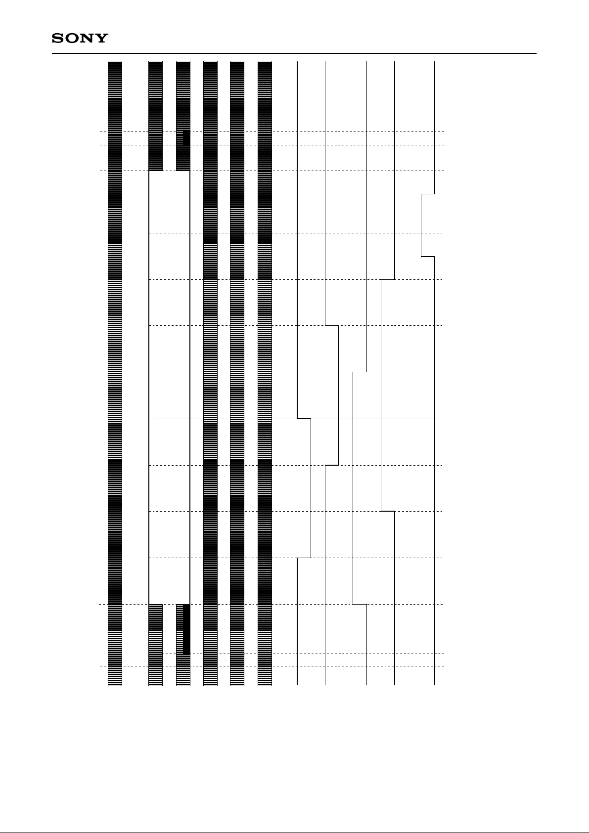
Drive Timing Chart (Vertical Sync) Progressive Scan Mode
VD
HD
1252
1251
1250
1249
V1
V2
– 21 –
V3
V4
1236
1236
1235
CCD
OUT
36MHz
Note) The 1252H horizontal period at 36MHz is 480clk; the 1493H horizontal period at 28MHz is 1860clk.
296
ICX274AQ
132
96
90
541
154
54 1
114
1
78
136
91
60
1
135
Drive Timing Char t (Horizontal Sync) Progressive Scan Mode
1
1920
CLK
1521 112128204
14
H1A/H1B
H2A/H2B
RG
SHP
SHD
18 1
1
– 22 –
V1
1
V2A/V2B/V2C
1 90
1
V3A/V3B/V3C
V4
1
1
SUB
 Loading...