Sony ICFCD-830 Service manual
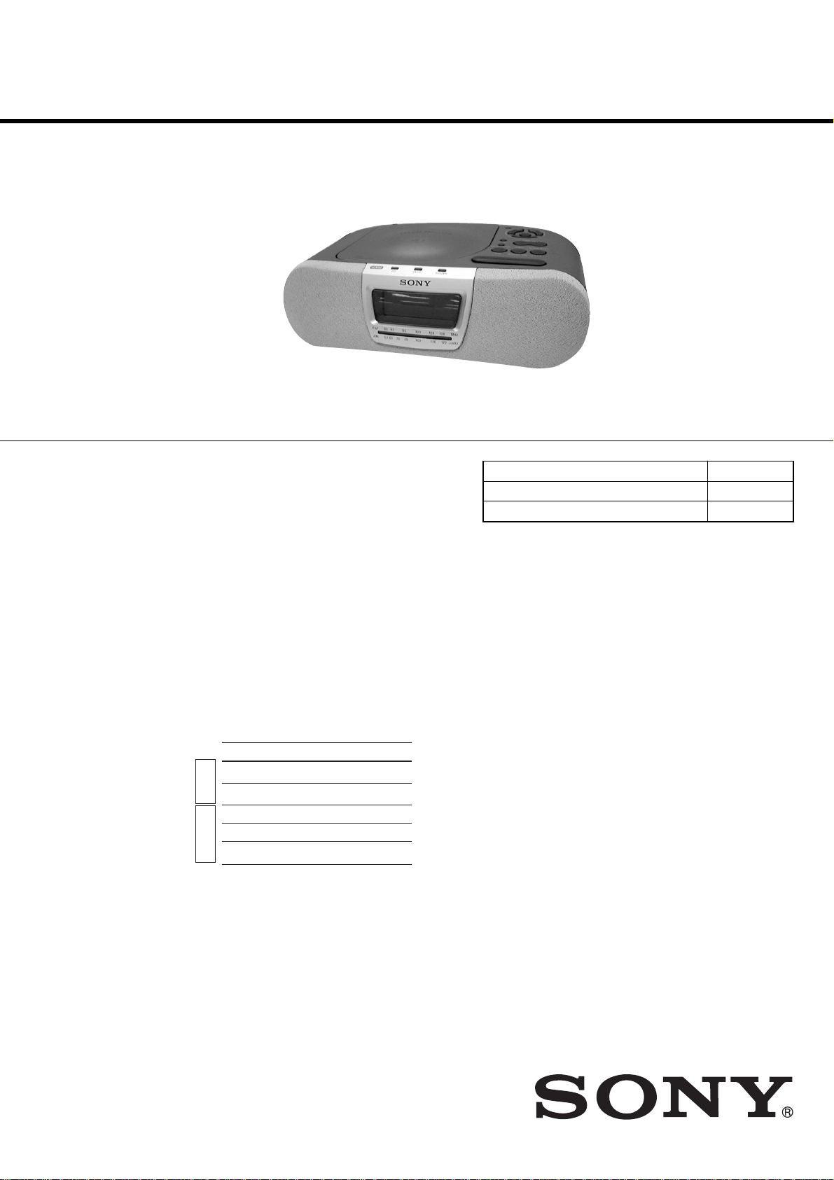
ICF-CD830/CD830L
SERVICE MANUAL
Ver 1.1 2001. 08
With SUPPLEMENT-1
Photo : ICF-CD830
SPECIFICATIONS
CD player section
System: Compact disc digital audio system
Laser diode properties: Material: GaAlAs
Wavelength: 780 nm
Emission duration: Continuous
Laser output: Less than 44.6 µW
(This output is the value measured at a
distance of about 200 mm from the objective
lens surface on the optical pick-up block
with 7 mm aperture.)
Frequency response: 20-20 000 Hz
Wow and flutter: Below measurable limit
Radio section
Frequency range:
ICF-CD830 ICF-CD830L
FM 87.5-108 MHz
America
AM 530-1 710 kHz
North and South
FM 87.5-108 MHz 87.5-108 MHz
AM(MW) 530-1 710 kHz 530-1 710 kHz
Other
countries
LW
–
+1
dB
–1.5
–
–
153-255 kHz
US Model
Canadian Model
Australian Model
E Model
ICF-CD830
AEP Model
ICF-CD830/CD830L
UK Model
ICF-CD830L
Model Name Using Similar Mechanism ICF-CD823
Optical Device Name KSM-213CDM
Optical Pick-UP Name KSS-213C
General
Time display:
North and South America, UK and
Australia: 12-hour system
Other countries: 24-hour system
Speaker:
66 mm (2
Power outputs:
1.2 W + 1.2 W
Power requirements:
North and South American model:
Australian model:
Other models:
Dimensions:
Approx. 273 × 94.5 × 194.5 mm (w/h/d)
(Approx. 10
projecting parts and controls
Mass:
Approx. 1 705 g (3 lb. 12 oz.)
ICF-CD830L (UK model):
Approx. 1 725 g (3 lb. 13 oz.)
Design and specifications are subject to change
without notice.
5
⁄8 inches) dia., 4 Ω
(at 10% harmonic distortion)
120 V AC, 60 Hz
240 V AC, 50 Hz
220-230 V AC, 50 Hz
3
⁄4 × 3 3⁄4 × 7 3⁄4 inches) incl.
9-873-107-12
2001H1600-1
© 2001.8
CD CLOCK RADIO
Sony Corporation
Personal Audio Company
Shinagawa Tec Service Manual Production Group
ICF-CD830/CD830L
r
TABLE OF CONTENTS
1. GENERAL ········································································ 4
2. DISASSEMBLY
2-1. UPPER CASE ······························································· 5
2-2. KEY BOARD ································································ 5
2-3. TRANSFORMER BOARD··········································· 6
2-4. MAIN CHASSIS ··························································· 6
2-5. OPTICAL PICK-UP BLOCK (KSM-213CDM) ·········· 6
3. TEST MODE ·······························································7
4. ELECTRICAL ADJUSTMENTS ····························· 9
5. DIAGRAMS
5-1. CIRCUIT BOARDS LOCATION ······························· 10
5-2. BLOCK DIAGRAM (CD830) ···································· 11
5-3. BLOCK DIAGRAM (CD830L) ·································· 12
5-4. SCHEMATIC DIAGRAM
– TUNER SECTION (CD830) –································· 13
5-5. SCHEMATIC DIAGRAM
– TUNER SECTION (CD830L) – ······························ 14
5-6. SCHEMATIC DIAGRAM
– CD SECTION – ······················································· 15
5-7. SCHEMATIC DIAGRAM
– POWER SECTION – ··············································· 16
5-8. PRINTED WIRING BOARD
– MAIN SECTION – ·················································· 17
5-9. PRINTED WIRING BOARD
– KEY/POWER SECTION – ······································ 18
5-10.SCHEMATIC DIAGRAM
– KEY SECTION – ····················································· 19
5-11.IC BLOCK DIAGRAMS ············································ 20
5-12.IC PIN FUNCTION DESCRIPTION ························· 22
SAFETY CHECK-OUT
After correcting the original service problem, perform the following
safety check before releasing the set to the customer:
Check the antenna terminals, metal trim, “metallized” knobs, screws,
and all other exposed metal parts for AC leakage.
Check leakage as described below.
LEAKAGE TEST
The AC leakage from any exposed metal part to earth ground and
from all exposed metal parts to any exposed metal part having a
return to chassis, must not exceed 0.5 mA (500 microampers.).
Leakage current can be measured by any one of three methods.
1. A commercial leakage tester, such as the Simpson 229 or RCA
WT-540A. Follow the manufacturers’ instructions to use these
instruments.
2. A battery-operated AC milliammeter. The Data Precision 245
digital multimeter is suitable for this job.
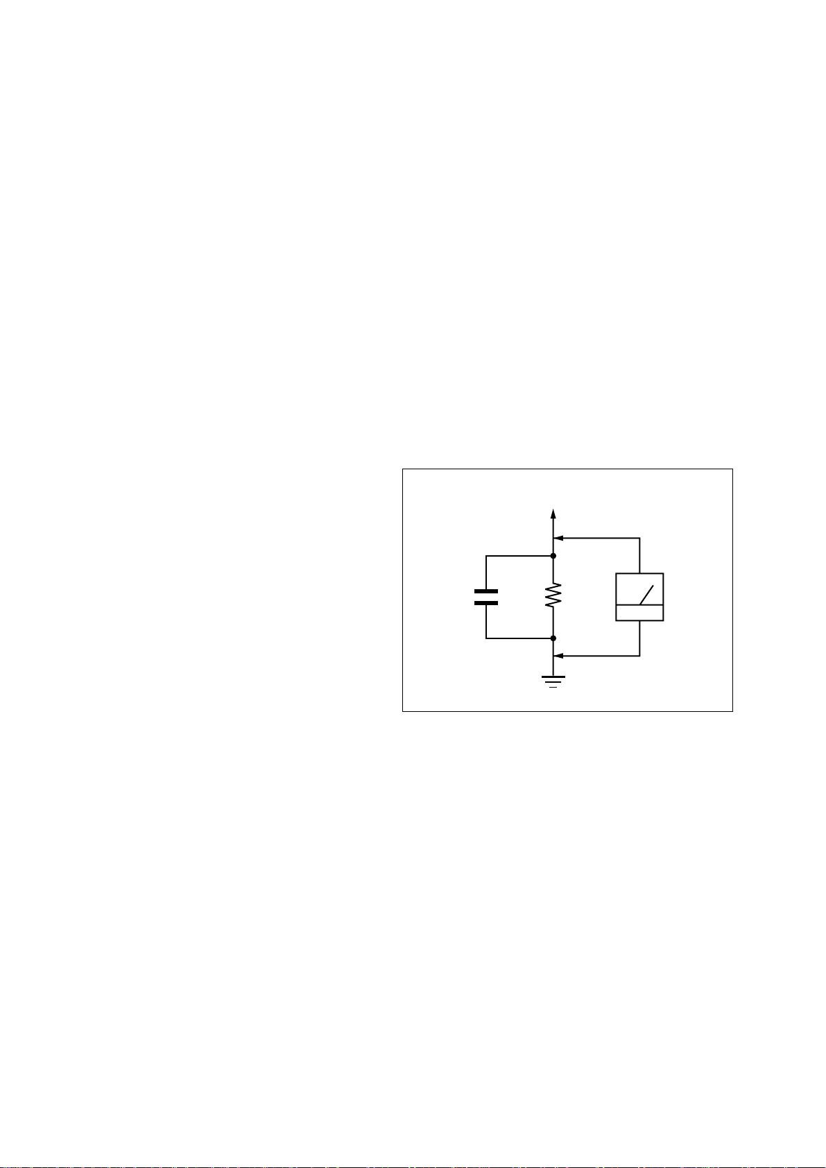
3. Measuring the voltage drop across a resistor by means of a VOM
or battery-operated AC voltmeter. The “limit” indication is 0.75
V, so analog meters must have an accurate low-voltage scale.
The Simpson 250 and Sanwa SH-63Trd are examples of a
passive VOM that is suitable. Nearly all battery operated digital
multimeters that have a 2 V AC range are suitable. (See Fig. A)
To Exposed Metal
Parts on Set
AC
0.15 µF
1.5 k
Ω
voltmete
(0.75 V)
6. EXPLODED VIEWS
6-1. CABINET SECTION ·················································· 23
6-2. CHASSIS SECTION··················································· 24
6-3. OPTICAL PICK-UP SECTION
(KSM-213CDM) ························································· 25
7. ELECTRICAL PARTS LIST ································· 26
SAFETY-RELATED COMPONENT WARNING!!
COMPONENTS IDENTIFIED BY MARK ! OR DOTTED LINE
WITH MARK ! ON THE SCHEMATIC DIAGRAMS AND IN
THE PARTS LIST ARE CRITICAL TO SAFE OPERATION.
REPLACE THESE COMPONENTS WITH SONY PARTS WHOSE
PART NUMBERS APPEAR AS SHOWN IN THIS MANUAL OR
IN SUPPLEMENTS PUBLISHED BY SONY.
ATTENTION AU COMPOSANT AYANT RAPPORT
À LA SÉCURITÉ!
LES COMPOSANTS IDENTIFIÉS PAR UNE MARQUE ! SUR
LES DIAGRAMMES SCHÉMATIQUES ET LA LISTE DES
PIÈCES SONT CRITIQUES POUR LA SÉCURITÉ DE
FONCTIONNEMENT. NE REMPLACER CES COM- POSANTS
QUE PAR DES PIÈCES SONY DONT LES NUMÉROS SONT
DONNÉS DANS CE MANUEL OU DANS LES SUPPLÉMENTS
PUBLIÉS PAR SONY.
Earth Ground
Fig. A. Using an AC voltmeter to check AC leakage.
Note on chip component replacement
• Never reuse a disconnected chip component.
• Notice that the minus side of a tantalum capacitor may be dam-
aged by heat.
2
ICF-CD830/CD830L
NOTES ON HANDLING THE OPTICAL PICK-UP
BLOCK OR BASE UNIT
The laser diode in the optical pick-up block may suffer electrostatic
break-down because of the potential difference generated by the
charged electrostatic load, etc. on clothing and the human body.
During repair, pay attention to electrostatic break-down and also
use the procedure in the printed matter which is included in the
repair parts.
The flexible board is easily damaged and should be handled with
care.
NOTES ON LASER DIODE EMISSION CHECK
The laser beam on this model is concentrated so as to be focused on
the disc reflective surface by the objective lens in the optical pickup block. Therefore, when checking the laser diode emission,
observe from more than 30 cm away from the objective lens.
CHUCK PLATE JIG ON REPAIRING
On repairing CD section, playing a disc without the CD lid, use
Chuck Plate Jig.
• Code number of Chuck Plate Jig: X-4918-255-1
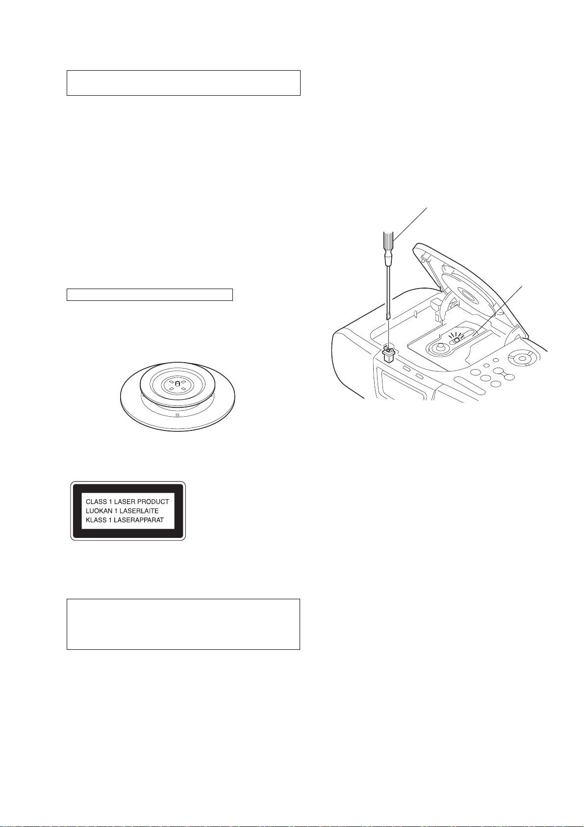
LASER DIODE AND FOCUS SEARCH
OPERATION CHECK
1. Open the CD lid.
2. Turn on S401 as following figure.
3. Confirm that the laser diode emission while observing the
objecting lens. When there is no emission, Auto Power Control
circuit or Optical Pick-up is broken.
Objective lens moves up and down once for the focus search.
Insert a precision
screwdriver and
push S401
laser diode
emission
This Compact Disc player is classified as a CLASS 1
LASER product.
The CLASS 1 LASER PRODUCT label is located on the
bottom exterior.
CAUTION
Use of controls or adjustments or performance of procedures
other than those specified herein may result in hazardous
radiation exposure.
3
ICF-CD830/CD830L
AC power cord
Cordon d’alimentation
secteur
FM wire antenna
Antenne fil FM
VOLUME
SECTION 1
GENERAL
ICF-CD830
This section is extracted from
instruction manual.
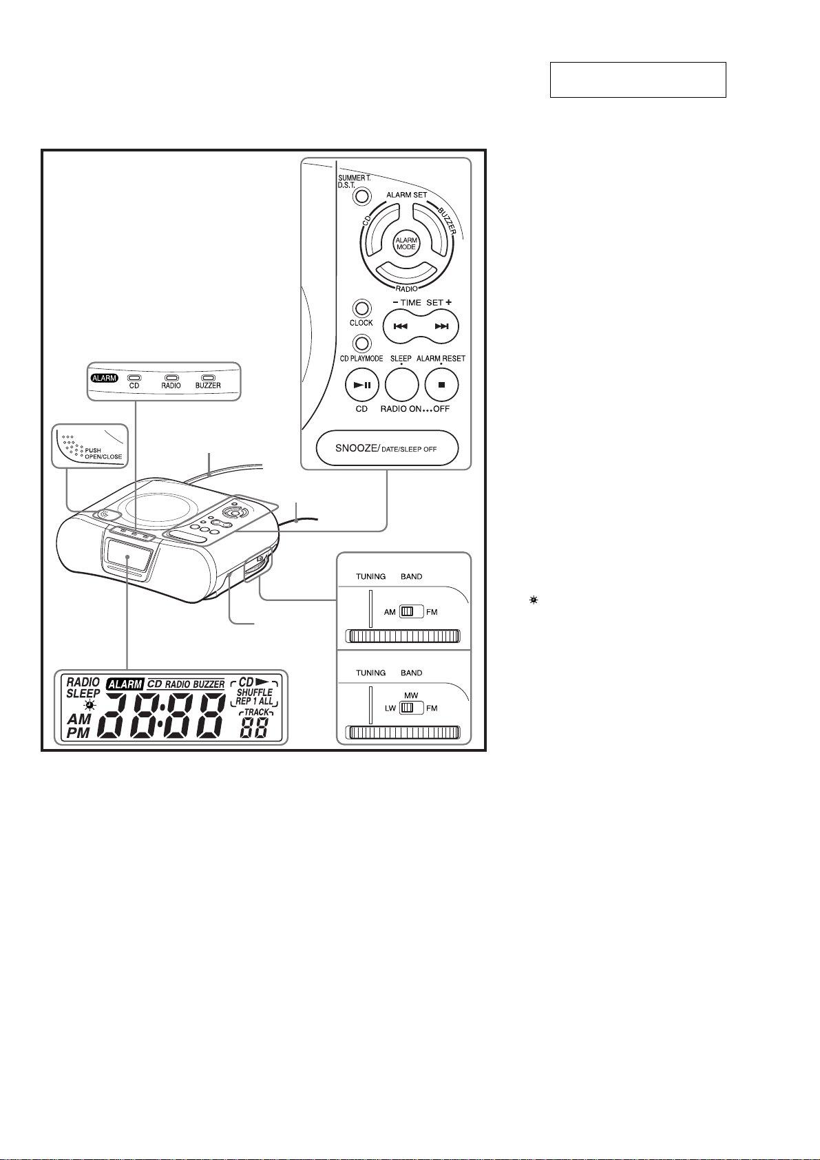
Setting the Clock
and Date
1
Plug in the clock radio.
The display will flash “AM 12:00” or “0:00”.
2
Press CLOCK for a few seconds.
You will hear a beep and the year will start to
flash in the display.
3
Press TIME SET + or – until the correct
year appears in the display.
4
Press CLOCK once.
5
Repeat steps 3 and 4 to set the month,
day, hour, and minute.
After setting the minute, press CLOCK to start
the counting of the seconds, and you will
hear two short beeps.
• To display the year and date, press SNOOZE/
DATE/SLEEP OFF once for the date, and within
2 seconds press it again for the year. The
display shows the date or year for a few
seconds and then changes back to the current
time.
• To set the current time rapidly, hold down
TIME SET + or –.
• The clock system varies depending on the
model you own.
12-hour system: “AM 12:00” = midnight
24-hour system: “0:00” = midnight
• In step 5, when you press CLOCK after the
minute setting to activate the clock, the seconds
start counting from zero.
To change the display to the
daylight saving time (summer time)
indication
Press D.S.T./SUMMER T.
“
” is displayed and the time indication
changes to summer time.
To deactivate the summer time function, press
D.S.T./SUMMER T. again.
ICF-CD830L
4
SECTION 2
d
)
DISASSEMBLY
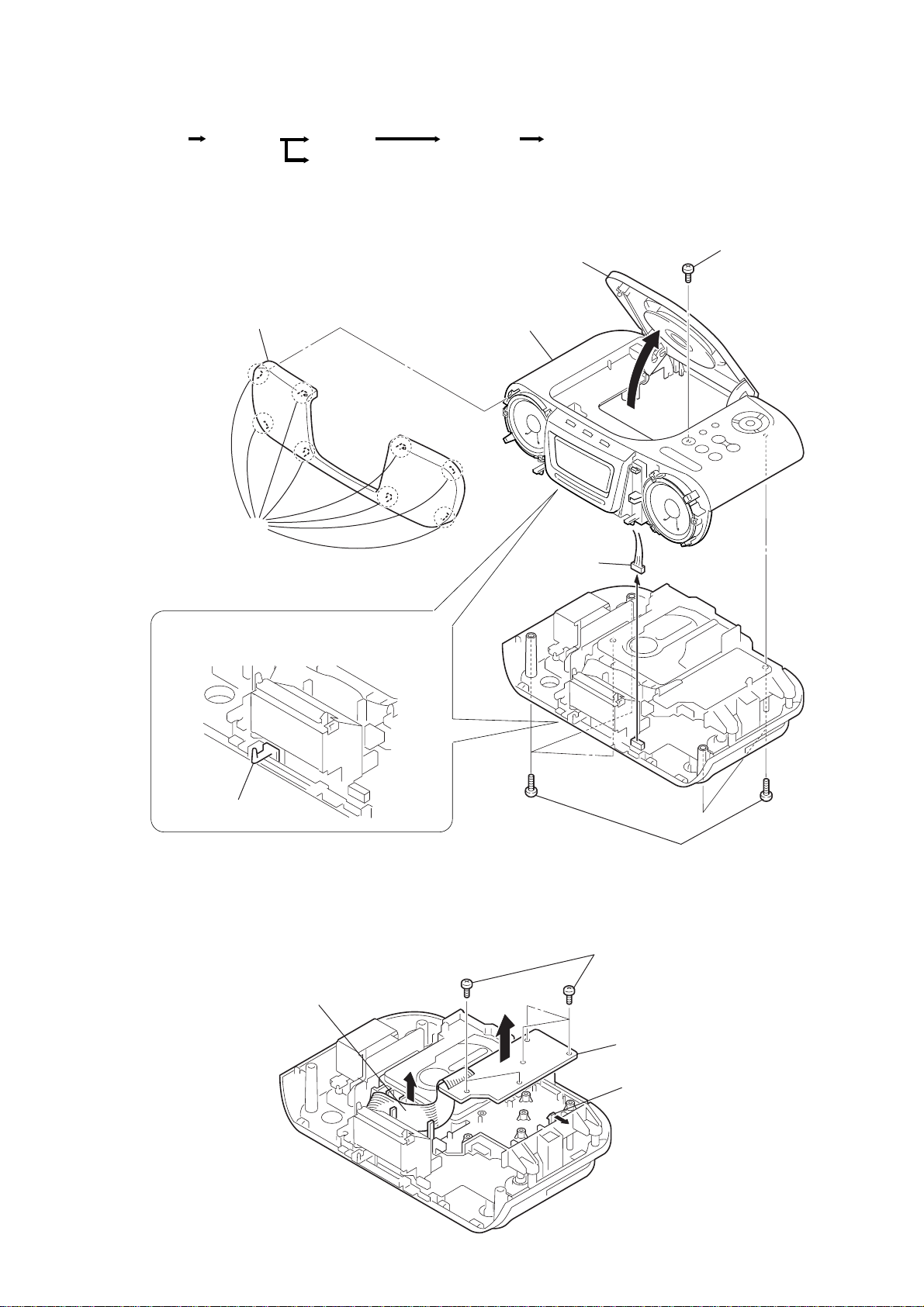
• The equipment can be removed using the following procedure.
Set
Upper case
Note: Follow the disassembly procedure in the numerical order given.
Key board
Transformer board
2-1. UPPER CASE
Main chassis Optical pick-up block (KSM-213CDM
ICF-CD830/CD830L
Ver 1.1 2001.08
5 Screw (+P3 × 14)
4 Lid, CD
2 Panel (SP)
1 Eight claws
Precaution during installation
When installing the upper case to the main section,
move the pointer to the left-most end as shown.
7 Upper case
6 Connector
(CN371)
Pointer
2-2. KEY BOARD
3 Five screws (+P3 × 14)
1 Five screws
(+P3 × 10)
4 Wire
3 Key boar
2 Hook
5
ICF-CD830/CD830L
k
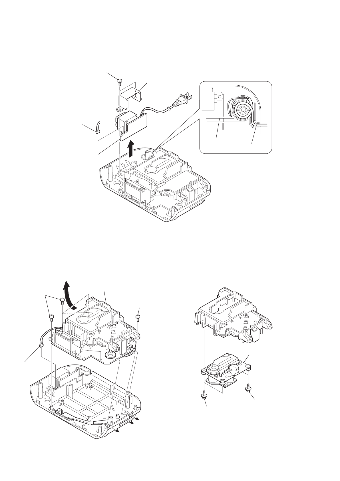
2-3. TRANSFORMER BOARD
2 Two screws
(+P3 × 10)
1 Connector
(CN901)
4 Transformer board
3 Bracket (Trans)
Transformer board
Power cord
2-4. MAIN CHASSIS
2 Six screws
(+P3 × 10)
3 Connector
(CN901)
4 Main chassis
1 Two screws
(+P3 × 10)
2-5. OPTICAL PICK-UP BLOCK (KSM-213CDM)
3 Optical pick-up bloc
(KSM-213CDM)
1 Two screws
2 Two screws
(2.6 × 10)
(2.6 × 10)
6
SECTION 3
TEST MODE
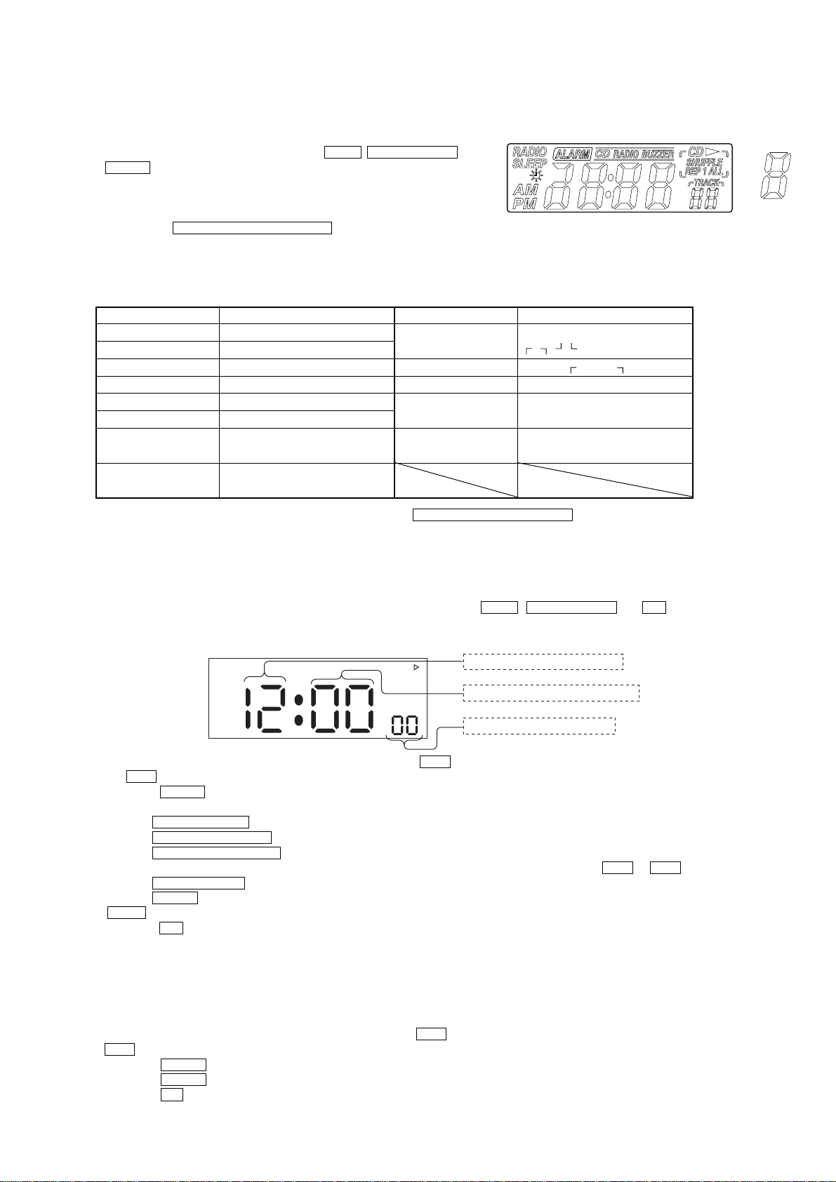
3-1. LCD Test Mode
• The LCD test mode is initiated by turning off the main power once then
back on or by resetting the machine while IC401 pin-60 terminal is
connected to GND, or while depressing the D.S.T. , ALARM MODE and
RADIO keys simultaneously.
• The LCD test mode operations are listed in the following table.
• When the machine enters the LCD test mode, the version number of the
system control IC is displayed on the LCD.
• Pressing the SNOOZE/DATE/SLEEP OFF key turns on all segments of
LCD and LEDs.
• Pressing any key turns off the corresponding segment of the LCD.
Correspondence between the keys and segments of LCD are as follows.
ICF-CD830/CD830L
(LCD segment)
a
fgb
ce
d
1234 56
KEY
D.S.T.
ALARM MODE
ALARM SET CD
ALARM SET BUZZER
ALARM SET RADIO
CLOCK
TIME SET –
TIME SET +
s
ALARM CD RADIO BUZZER
ALARM-CD LED
ALARM-BUZZER LED
ALARM-RADIO LED
AM, PM,:
1a, 1b, 1c, 1d, 1e, 1f, 1g,
2a, 2b, 2c, 2d, 2e, 2f, 2g
3a, 3b, 3c, 3d, 3e, 3f, 3g,
4a, 4b, 4c, 4d, 4e, 4f, 4g
SEGMENT
KEY
CD PLAY MODE
CD
RADIO
OFF
SNOOZE/DATE/
SLEEP OFF
SEGMENT
REP, 1, ALL, SHUFFLE,
, , ,
CD, H, TRACK
RADIO, SLEEP
5a, 5b, 5c, 5d, 5e, 5f, 5g,
6a, 6b, 6c, 6d, 6e, 6f, 6g
• After all segments of LCD and LEDs turn off, pressing the SNOOZE/DATE/SLEEP OFF key ends the LCD test mode and resets the
machine.
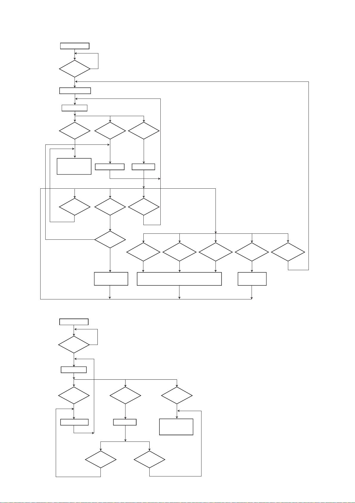
3-2. CD Test Mode
3-2-1. CD TEST-1 (AUTO)
• The CD TEST-1 (AUTO) mode is initiated by turning off the main power once then back on or by resetting the machine while IC401 pin59 terminal (RADIO LED) is connected to GND, or while depressing the D.S.T. , ALARM MODE and CD keys simultaneously.
• When the machine enters CD TEST-1 (AUTO) mode, it repeats the focus search until the focus becomes OK.
• After the focus becomes OK and the focus is automatically adjusted, rough servo is locked in and the adjustment value is displayed.
F-E BALANCE ADJUSTMENT
TRACKING GAIN ADJUSTMENT
FOCUS BIAS ADJUSTMENT
AM
CD
SHUFFLE
TRACK
• The sled can be moved to the innermost track by pressing the . button. The sled can be moved to the outermost track by pressing
the > button.
• When the RADIO button is pressed, the machine enters the CLVA (servo ON) and the mute is turned OFF if data is read successfully.
When the following button is pressed, the corresponding operations are performed.
a) ALARM SET CD Setting the 1 track jump
b) ALARM SET RADIO Setting the 10 track jump
c) ALARM SET BUZZER Setting the 100 track jump
Afterwards the desired track jump can be set by pressing the > or . button.
d) ALARM MODE TRACKING GAIN-UP
e) RADIO Rough servo
• D.S.T. restarts CD TEST-1 (AUTO) mode from the focus automatic adjustment
• When the CD button is pressed then, the track jumps to the second session and the machine exits the CD TEST-1 (AUTO) mode.
3-2-2. CD TEST-2 (MANUAL)
• The CD TEST-2 (MANUAL) mode is initiated by turning off the main power once then back on or by resetting the machine while IC401
pin-58 terminal (CD LED) is connected to GND.
• When the machine enters CD TEST-2 (MANUAL) mode, it repeats the focus search until the focus becomes OK.
• After the focus becomes OK, the machine enters the rough servo.
• The sled can be moved to the innermost track by pressing the . button. The sled can be moved to the outermost track by pressing the
> button.
• When the RADIO button is pressed, the machine enters the CLVA (servo ON) and the mute is turned OFF if data is read successfully.
When the RADIO button is pressed again, the machine enters the rough servo.
• When the CD button is pressed then, the track jumps to the second session and the machine exits the CD TEST-2 (MANUAL) mode.
7
ICF-CD830/CD830L
CD TEST-1
FOCUS
OK
Y
Auto adjustment
Rough servo
CD button
TEST MODE END
The second music
played back.
CD button
Y
N
± button
Sled movement
± button
Y : YES
N: NO
Servo ON
RADIO
button
YYY
RADIO
button
YY
CD TEST-2
FOCUS
OK
Y
Rough servo
± button
Y
jump has
been set?
N
Executes the
setting of jump.
N
Y
RADIO
button
ALARM SET
CD
Y
ALARM SET
RADIO
Y
YY Y Y
Sets the respective
setup values.
CD
button
Y
ALARM SET
BUZZER
ALARM
MODE
TRACKING
GAIN UP
D.S.T.
Sled movement
± button
Servo ON
CD
button
YY
TEST MODE END
The second music
played back.
8
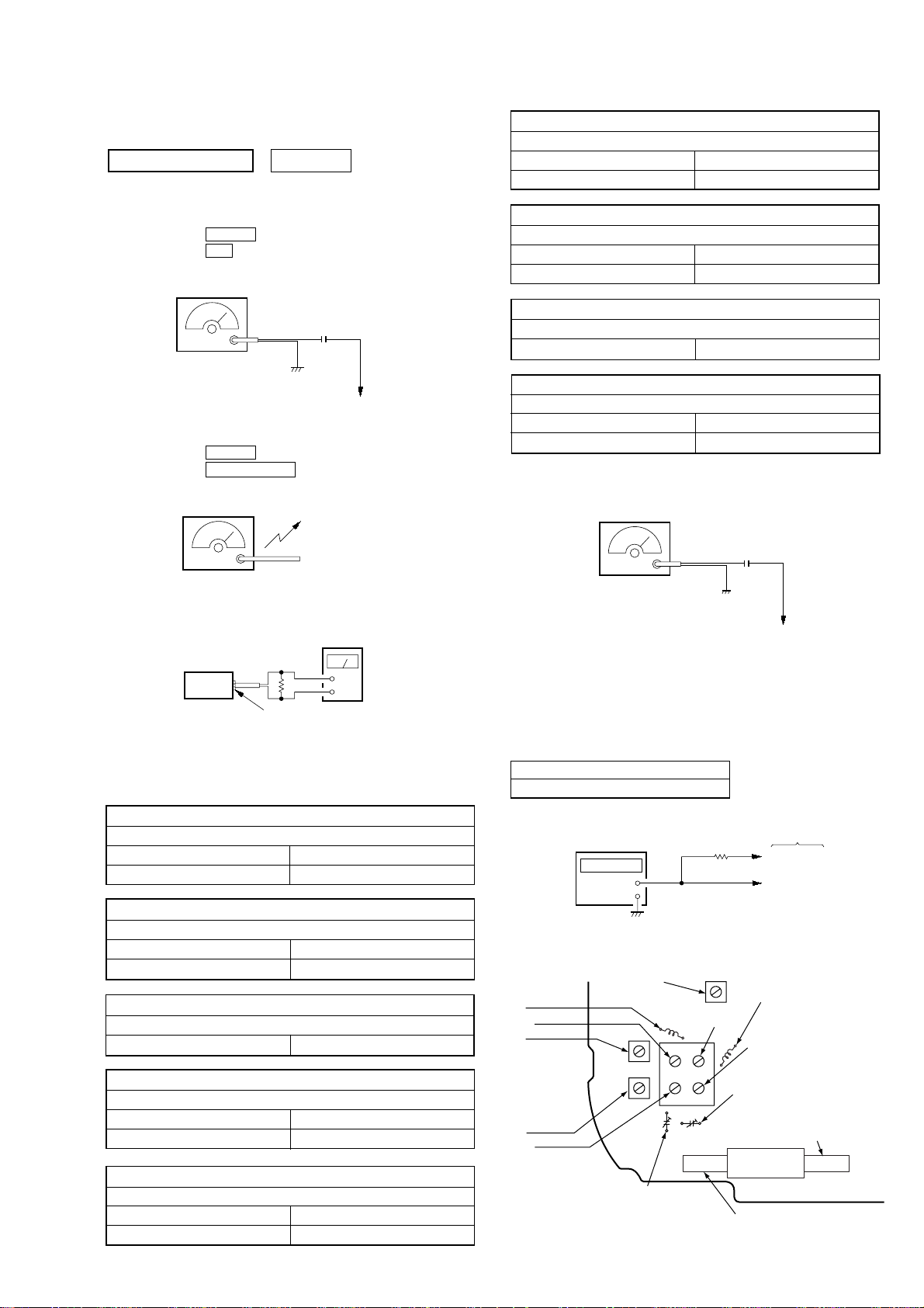
SECTION 4
FM RF signal
generator
Carrier frequency: 98 MHz
Modulation: no modulation
Output level: 0.1 V (100 dB)
0.01 µF
FM lead wire antenna terminal
d
t
nt
ELECTRICAL ADJUSTMENTS
ICF-CD830/CD830L
PRECAUTION
• Adjustment should be performed in the order given.
TUNER SECTION 0 dB=1 µV
[FM]
Setting:
Function switch : RADIO
BAND switch : FM
FM RF signal
generator
0.01 µF
75 kHz frequency deviation
by 1 kHz signal.
Output level: as low as possible
[AM (MW/LW) ]
Setting:
Function switch : RADIO
BAND switch : AM (MW/LW)
AM RF signal
generator
FM lead wire antenna terminal
Put the lead-wire
antenna close to
the set.
MW FREQUENCY COVERAGE ADJUSTMENT (CD830L)
Adjust for a maximum reading on level meter
L4 515 kHz
CT4 1,750 kHz
MW TRACKING ADJUSTMENT (CD830L)
Adjust for a maximum reading on level meter
L1-1 600 kHz
CT1 1,400 kHz
LW FREQUENCY COVERAGE ADJUSTMENT (CD830L)
Adjust for a maximum reading on level meter
CT6 145 kHz
LW TRACKING ADJUSTMENT (CD830L)
Adjust for a maximum reading on level meter
L1-2 160 kHz
CT5 240 kHz
FM VCO Adjustment
Procedure:
• Repeat the procedures in each adjustment several times, and the
frequency coverage and tracking adjustments should be finally
done by the trimmer capacitors.
AM FREQUENCY COVERAGE ADJUSTMENT (CD830)
30% amplitude modulation by
400 Hz signal.
Output level: as low as possible
level meter
4 Ω
set
SPEAKER OUT
FM FREQUENCY COVERAGE ADJUSTMENT
Adjust for a maximum reading on level meter
L3 86.5 MHz (87.35 MHz)
CT3 109.5 MHz (108.25 MHz)
FM TRACKING ADJUSTMENT
Adjust for a maximum reading on level meter
L2 86.5 MHz (87.35 MHz)
CT2 109.5 MHz (108.25 MHz)
AM IF ADJUSTMENT
Adjust for a maximum reading on level meter
T1 455 kHz
Adjust for a maximum reading on level meter
L4 515 kHz (516.5 kHz)
CT4 1,750 kHz (1,631.5 kHz)
AM TRACKING ADJUSTMENT (CD830)
Adjust for a maximum reading on level meter
L1 600 kHz
CT1 1,400 kHz
+
–
( ) : AEP Model
1. Connect the frequency counter to 4 and 7 pins of IC1 as shown
the figure right.
2. Tune the set to 98 MHz.
3. Adjust RV1 for 76 kHz reading on frequency counter.
Specification V alue:
Frequency counter
75,950 – 76,050 Hz
Connection:
frequency counter
+
–
33 k Ω
MAIN Boar
IC1 Pin 7
IC1 Pin 4
Adjustment Location:
[MAIN BOARD] (Component Side)
T1
L3
CT3
L3
FM Frequency
Coverage
Adjustment
L4
CT4
AM Frequency
Coverage Adjustment
MW Frequency
Coverage Adjustment
AM IF
Adjustment
CT6
LW Frequency
Coverage
Adjustment
CT2
L2
FM Traking
Adjustment
CT1
AM Tracking Adjustmen
MW Tracking Adjustme
CT5
LW Traking Adjustment
L1-2
LW Traking Adjustment
L1, L1-1
AM Tracking Adjustment
MW Tracking Adjustment
9
ICF-CD830/CD830L
SECTION 5
DIAGRAMS
Note on Printed Wiring Board:
• X : parts extracted from the component side.
• : Pattern from the side which enables seeing.
Note on Schematic Diagrams:
• All capacitors are in µF unless otherwise noted. pF: µµF
50 WV or less are not indicated except for electrolytics
and tantalums.
• All resistors are in Ω and 1/
specified.
¢
•
• 2 : nonflammable resistor.
• C : panel designation.
• H : adjustment for repair.
• A : B+ Line.
• Voltages and waveforms are dc with respect to ground
Note:
The components identified by mark ! or dotted
line with mark ! are critical for safety.
Replace only with part
number specified.
• Voltages are taken with a VOM (Input impedance 10 MΩ).
• Signal path.
• Abbreviation
: internal component.
under no-signal (detuned) conditions.
no mark : FM
( ) : AM (MW/LW)
< > : CD
Voltage variations may be noted due to normal production tolerances.
F : FM
f : AM (MW/LW)
J : CD
AUS : Australian model
CND : Canadian model
IT : Italian model
SP : Singapore model
4
W or less unless otherwise
Note:
Les composants identifiés par
une marque ! sont critiques
pour la sécurité.
Ne les remplacer que par une
piéce portant le numéro
spécifié.
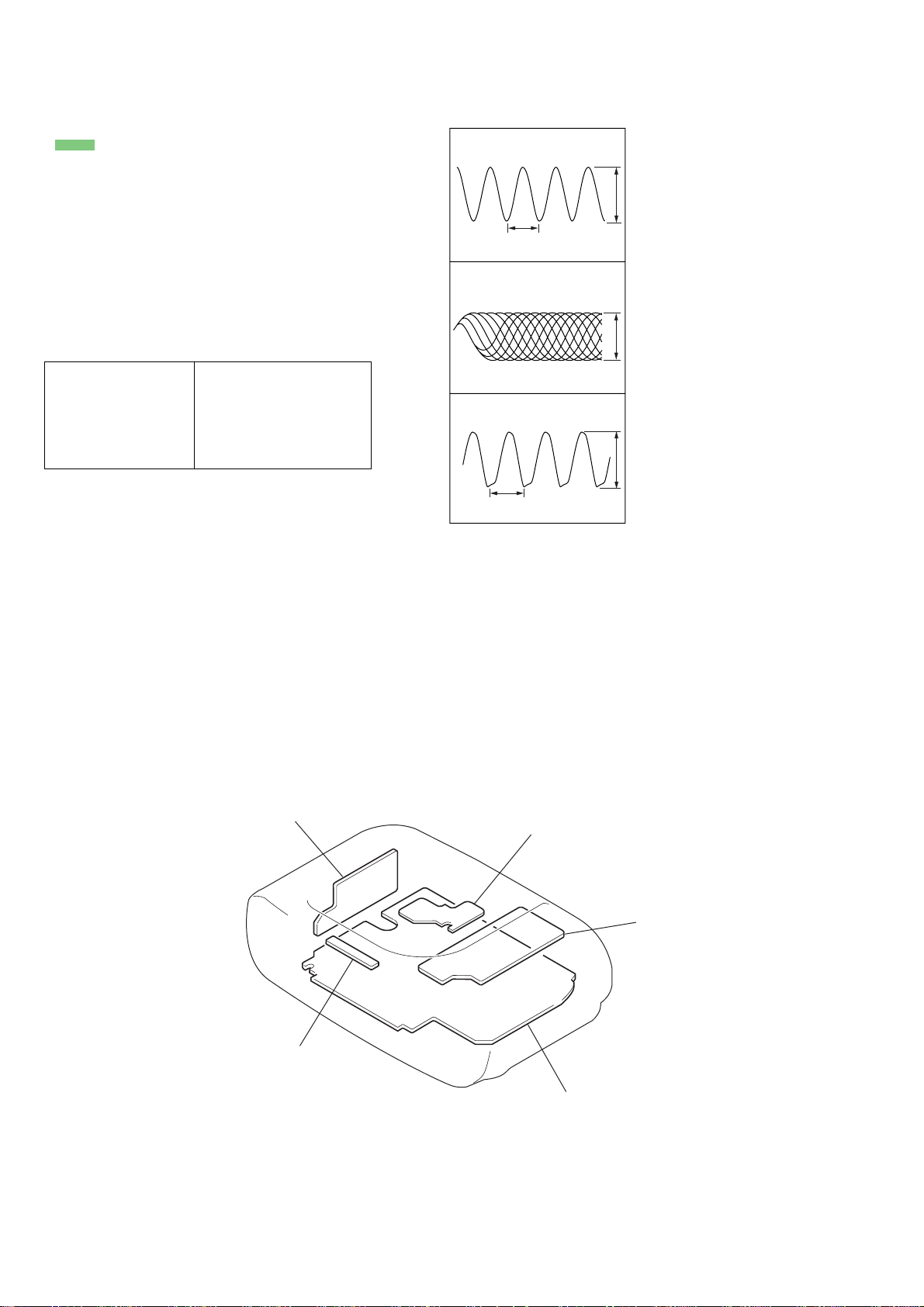
• Waveforms
1
IC401 ud (XT1)
31 ms
1.0 V/DIV, 20 ms/DIV
2
IC501 ed (RF0)
(PLAY MODE)
0.2 V/DIV, 500 ns/DIV
3
IC551 ua (XTA0)
59 ns
2.0 V/DIV, 40 ns/DIV
3.4 Vp-p
0.9 – 1.3 Vp-p
5.6 Vp-p
5-1. CIRCUIT BOARDS LOCATION
TRANSFORMER board
LED board
MOTOR (6P) board
KEY board
MAIN board
10
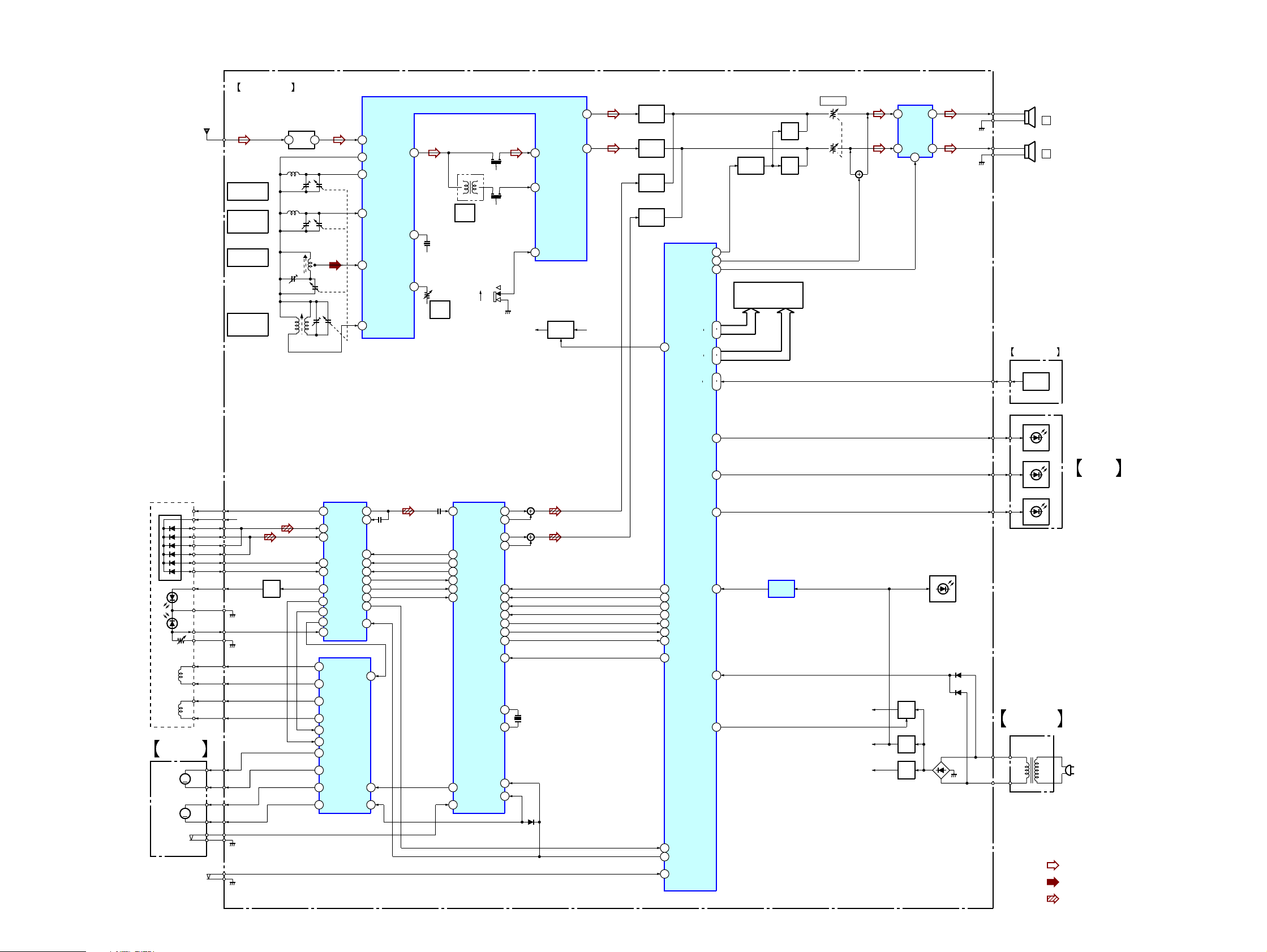
5-2. BLOCK DIAGRAM (CD830)
ANT1
(FM ANTENNA)
TRACKING
FREQUENCY
COVERAGE
TRACKING
FREQUENCY
COVERAGE
MAIN BOARD
FM
FM
AM
AM
AM OSC
BPF1
B.P.F
1
L2
CT2 CV1-2
FM RF
L3
CT3
FM OSC
L1
AM FERRITE-ROD
ANTENNA
CT1
L4
CT4
3
CV1-3
CV1-1
CV1-4
18
21
20
22
19
24
FRONT- END
FM RF IN
REG
FM RF OUT
FM OSC
AM RF
AM OSC
FM/AM
IC1
MIX OUT
DISCRI
VCO
ICF-CD830/CD830L
RV351
L OUT
6
CF3
AM IFT
AM
IF
10.7MHz
T1
CF2
455kHz
S1
FM
AM
13
14
15
16
26
CF1
27
RV1
FM
VCO
FM IF
AM IF
BAND
+B SW
Q1
R OUT
5
+5VTU +B
BUFFER
Q131
BUFFER
Q231
BUFFER
Q101
BUFFER
Q201
SYSTEM CONTROL
IC401
POWER ON
80
RADIO ON
A MUTE
BUZZER
SEG0
SEG15
COM0
COM3
KEY0
KEY12
MUTE
Q151
MUTE
CONT
Q351
77
53
79
LIQUID CRYSTAL
11
26
7
10
33
47
LCD401
DISPLAY PANEL
MUTE
Q251
VOLUME
11
POWER AMP
IC371
12
3
5
8
SP101
SP201
L
(SPEAKER)
R
KEY BOARD
S601-613
FUNCTION
KEY
OPTICAL PICK-UP
BLOCK
(KSS-213C)
VC
A
B
C
D
E
F
LD
GND
PD
VR
F+
FOCUS
COIL
F-
T+
TRACKING
COIL
T-
MOTOR(6P)
BOARD
M571
SLED
M
MOTOR
M572
SPINDLE
M
MOTOR
D653
ALM-CD LED
58
D652
DIGITAL SERVO
RF AMP
IC501
51
RFO
+5V
Q501
LD
DRIVE
VC
38
PD1
39
PD2
42
E
41
F
36
LD
16
SLO
13
TAO
6
FEO
37
PD
MOTOR/COIL DRIVE
26
F+
27
F-
17
T+
18
T-
19
T IN
3
SL IN
2
SL+
1
SL-
12
SP+
11
SP-
IC591
DATA
COUT
RFI
CLK
XLT
FOK
F IN
SP IN
MUTE
33
32
22
20
21
27
24
25SENS1
26SENS2
23XRST
25
15
7
DIGITAL SIGNAL PROC.
D/A CONV.
IC551
35
L OUT1
RF
A OUT1
L OUT2
A OUT2
12
DATO
14
CLKO
13
XLTO
18
FOK
11
10
21
15
CIN
SEIN
MDP
XLON MUTE
SPOA(LIMIT)
DATA
SENS
SMUTE
XTAI
XTAO
XRST
67
65
74
76
7
9CLK
8XLAT
4SQCK
57SCOR
5SQSO
6
62
71
X551
16.9344MHz
72
79
17
ALM-RADIO LED
ALM-BUZZER LED
56
C DATA
54
C CLOCK
55
C LATCH
62
C SQCK
52
C SCOR
61
C SQSO
50
C SENS
63
C MUTE
RESET
CD ON
59
D651
60
D401-402
67
49AC IN
57
RESET
IC402
IC402
CD +B
M +6V
D903
D905-908
D904
TRANSFORMER
BOARD
T901
POWER
TRANSFOMER
+B SW
Q551
+5V
REG
Q901
REG
Q903
AC
IN
LED
BOARD
S570
LIMIT
SW
S401
DOOR SW
51
64
75
C SENS2
C RST
DOOR IN
• Signal Path
: FM
: AM
: CD
1111
ICF-CD830/CD830L
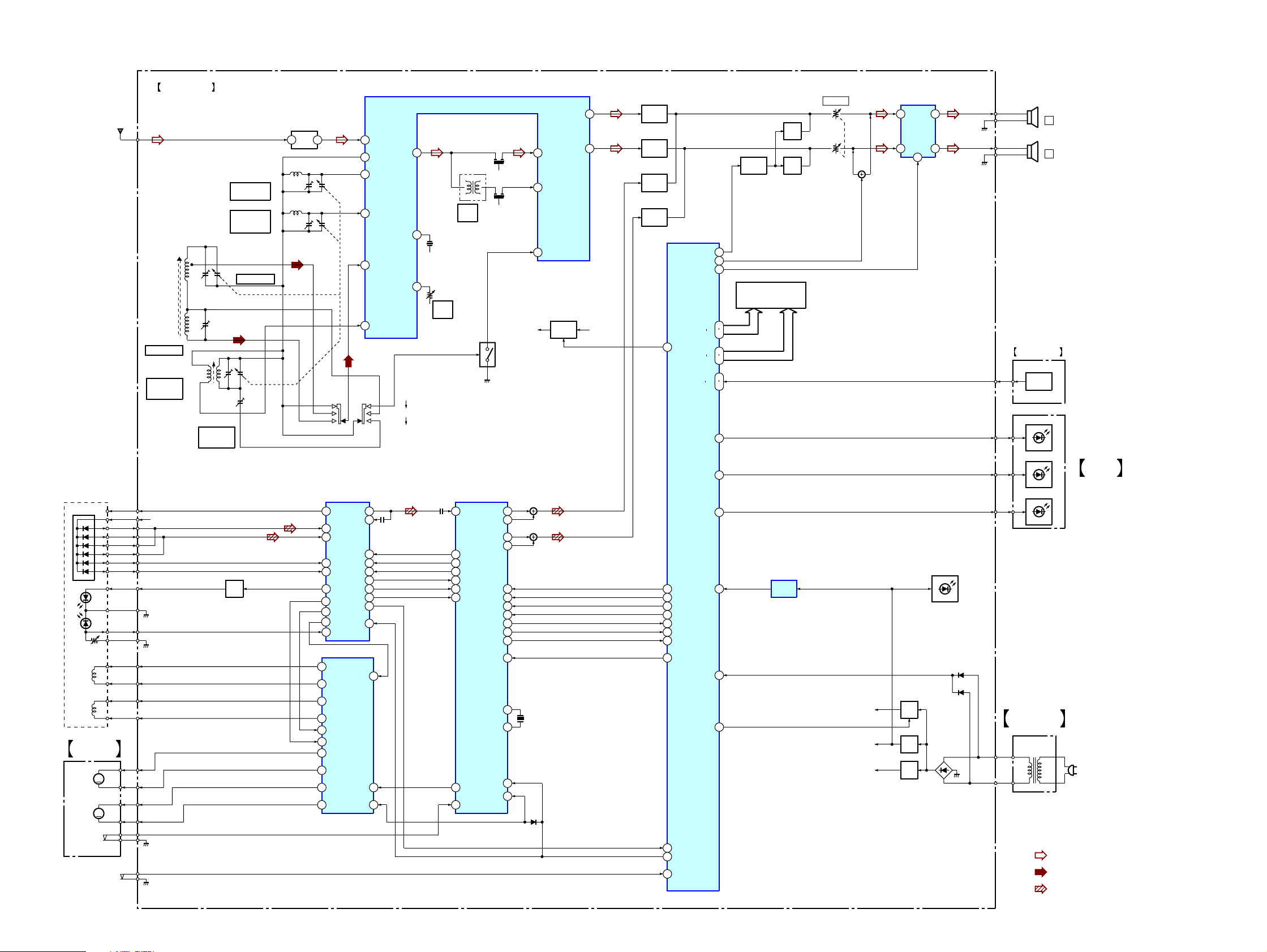
5-3. BLOCK DIAGRAM (CD830L)
MAIN BOARD
ANT1
(FM ANTENNA)
L1
MW/LW FERRITE-ROD
ANTENNA
L1-1
(MW)
L1-2
(LW)
L1-2,CT5
LW TRACKING
L4,CT4
MW
FREQUENCY
COVERAGE
OPTICAL PICK-UP
BLOCK
(KSS-213C)
VR
FOCUS
COIL
TRACKING
COIL
MOTOR(6P)
BOARD
M571
SLED
MOTOR
M572
SPINDLE
MOTOR
VC
A
B
C
D
E
F
LD
GND
PD
M
M
F+
F-
T+
T-
+5V
MW/LW
OSC
CT1
L4
FREQUENCY
COVERAGE
CT2,L2
FM
TRACKING
L3,CT3 CV1-3
FM
FREQUENCY
COVERAGE
CV1-1
L1-1,CT1
MW TRACKING
CT5
CV1-4
CT4
CT6
CT6
LW
Q501
LD
DRIVE
1
L2 CT2
FM RF
L3 CT3
FM OSC
BPF1
B.P.F
3
CV1-2
S1-1
RF AMP
IC501
51
VC
38
PD1
39
PD2
42
E
41
F
36
LD
16
SLO
13
TAO
6
FEO
37
PD
MOTOR/COIL DRIVE
IC591
26
F+
27
F-
17
T+
18
T-
19
T IN
3
SL IN
2
SL+
1
SL-
12
SP+
11
SP-
DATA
COUT
RFO
RFI
CLK
XLT
FOK
F IN
SP IN
MUTE
18
21
20
22
19
24
S1-2
FM RF IN
REG
FM RF OUT
FM OSC
AM RF
AM OSC
33
32
22
20
21
27
24
25SENS1
26SENS2
23XRST
25
15
7
FM/AM
FRONT- END
IC1
MIX OUT
DISCRI
VCO
RV351
L OUT
6
CF3
16
26
CF1
27
RV1
FM
VCO
FM
MW
LW
35
12
14
13
18
11
10
21
15
10.7MHz
T1
AM IFT
CF2
455kHz
AM
IF
Q2,Q3
DIGITAL SERVO
DIGITAL SIGNAL PROC.
D/A CONV.
IC551
L OUT1
RF
A OUT1
L OUT2
A OUT2
DATO
CLKO
XLTO
FOK
DATA
CIN
SEIN
SENS
SMUTE
XTAI
XTAO
XRST
MDP
XLON MUTE
SPOA(LIMIT)
13
14
15
67
65
74
76
7
9CLK
8XLAT
4SQCK
57SCOR
5SQSO
6
62
71
X551
16.9344MHz
72
79
17
FM IF
AM IF
BAND
+B SW
Q1
R OUT
5
+5VTU +B
BUFFER
Q131
BUFFER
Q231
BUFFER
Q101
BUFFER
Q201
SYSTEM CONTROL
IC401
POWER ON
80
RADIO ON
ALM-CD LED
ALM-RADIO LED
ALM-BUZZER LED
56
C DATA
54
C CLOCK
55
C LATCH
62
C SQCK
52
C SCOR
61
C SQSO
50
C SENS
63
C MUTE
A MUTE
BUZZER
SEG0
SEG15
COM0
COM3
KEY0
KEY12
RESET
CD ON
MUTE
Q151
MUTE
CONT
Q351
77
53
79
LIQUID CRYSTAL
11
26
7
10
33
47
58
59
60
67
49AC IN
57
LCD401
DISPLAY PANEL
RESET
IC402
IC402
MUTE
Q251
VOLUME
CD +B
M +6V
11
POWER AMP
IC371
12
3
5
8
SP101
SP201
L
(SPEAKER)
R
KEY BOARD
S601-613
FUNCTION
KEY
D653
D652
D651
D401-402
D903
D905-908
D904
TRANSFORMER
BOARD
T901
POWER
TRANSFOMER
+B SW
Q551
+5V
REG
Q901
REG
Q903
AC
IN
LED
BOARD
S570
LIMIT
SW
S401
DOOR SW
• Signal Path
51
64
75
C SENS2
C RST
DOOR IN
: FM
: MW/LW
: CD
1212
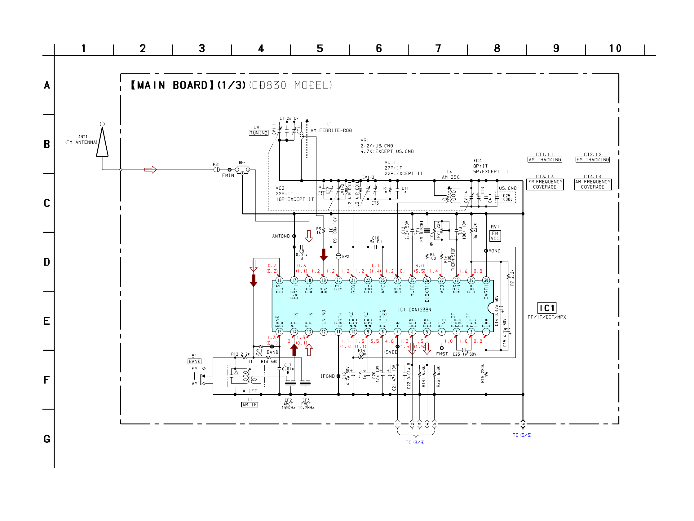
5-4. SCHEMATIC DIAGRAM – TUNER SECTION (CD830) –
ICF-CD830/CD830L
1313
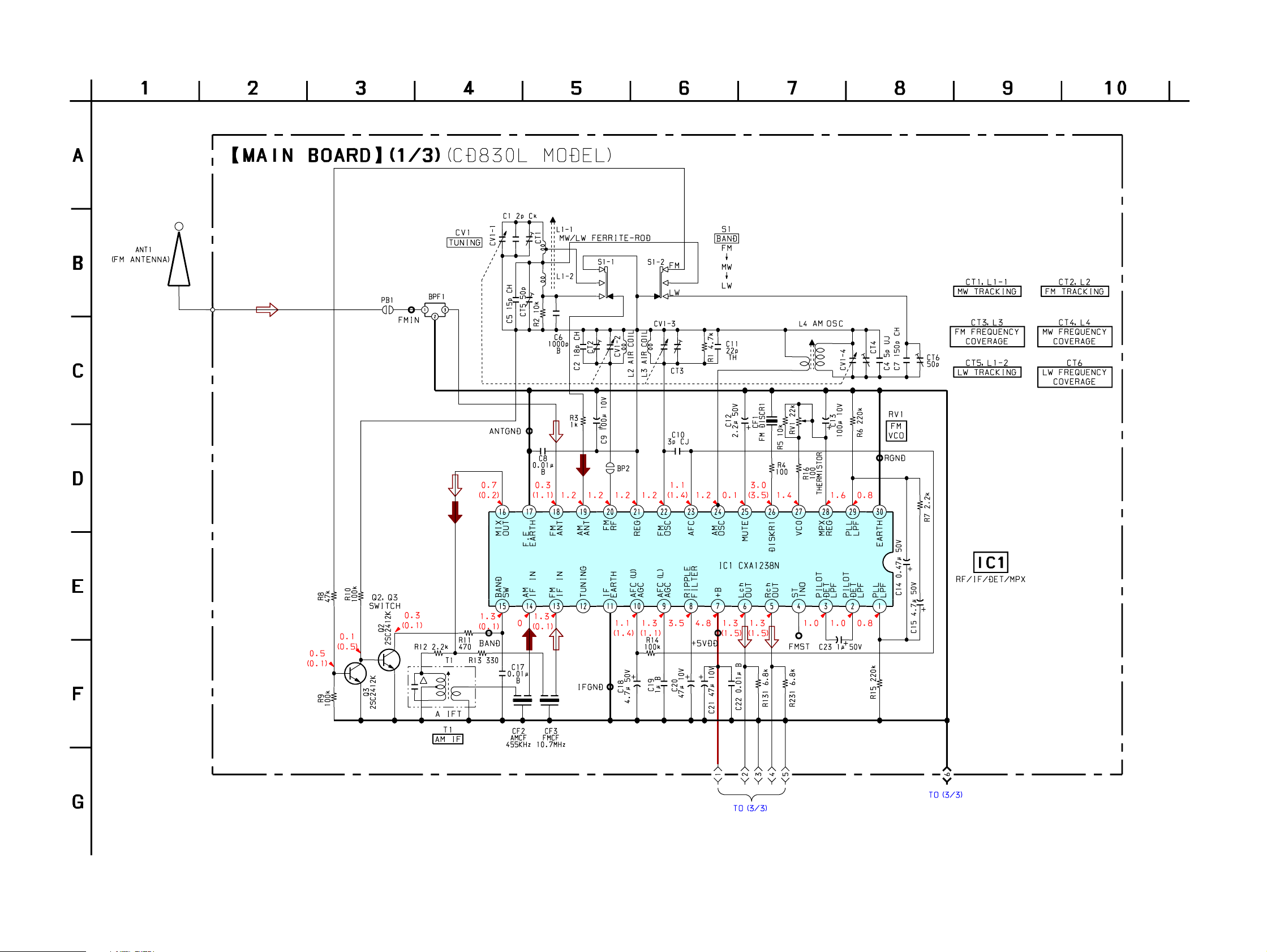
ICF-CD830/CD830L
5-5. SCHEMATIC DIAGRAM – TUNER SECTION (CD830L) –
1414
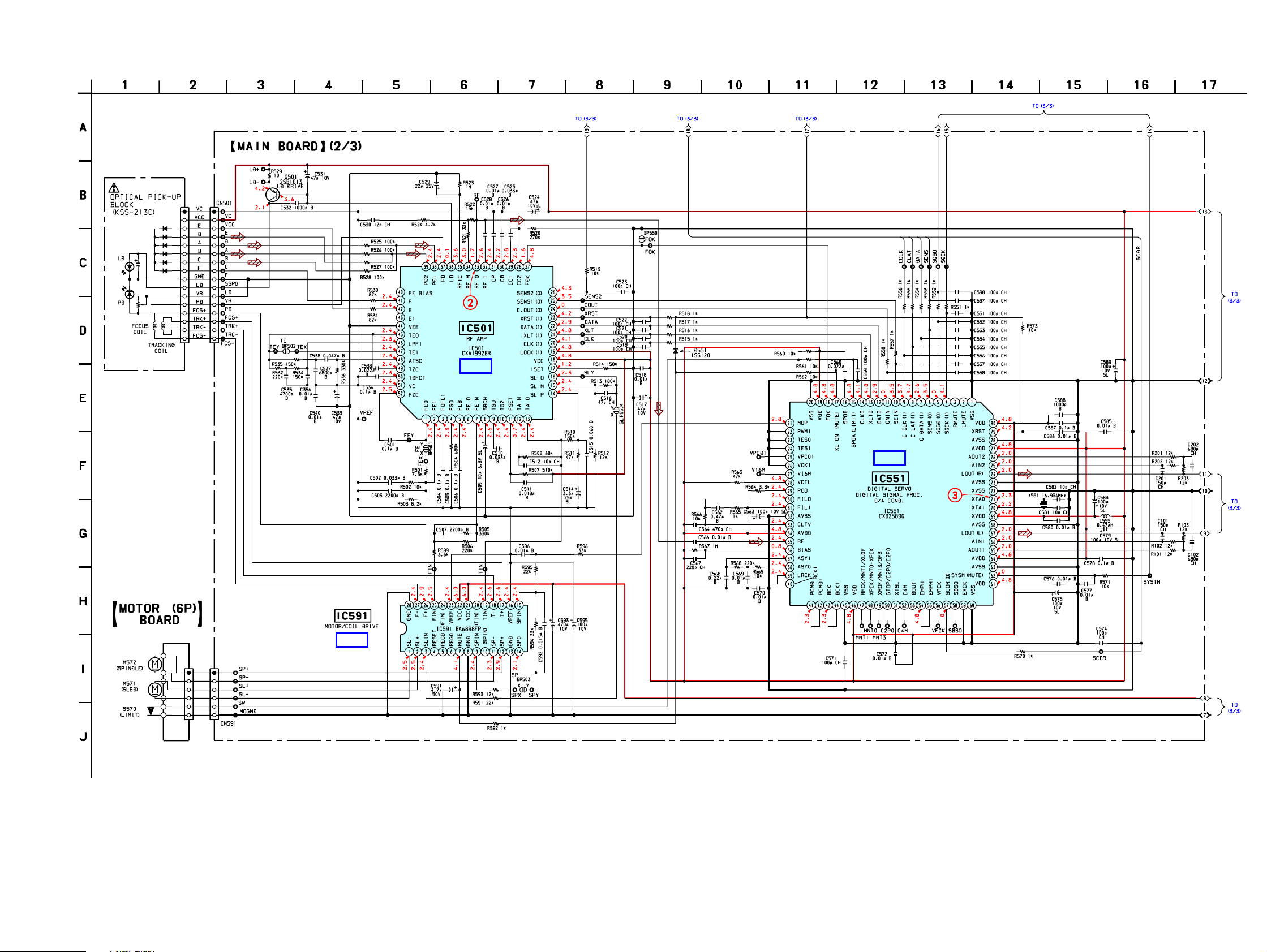
ICF-CD830/CD830L
5-6. SCHEMATIC DIAGRAM – CD SECTION –
• Refer to page 10 for Waveforms. • Refer to page 20, 21 for IC Block Diagrams.
IC B/D
IC B/D
IC B/D
1515
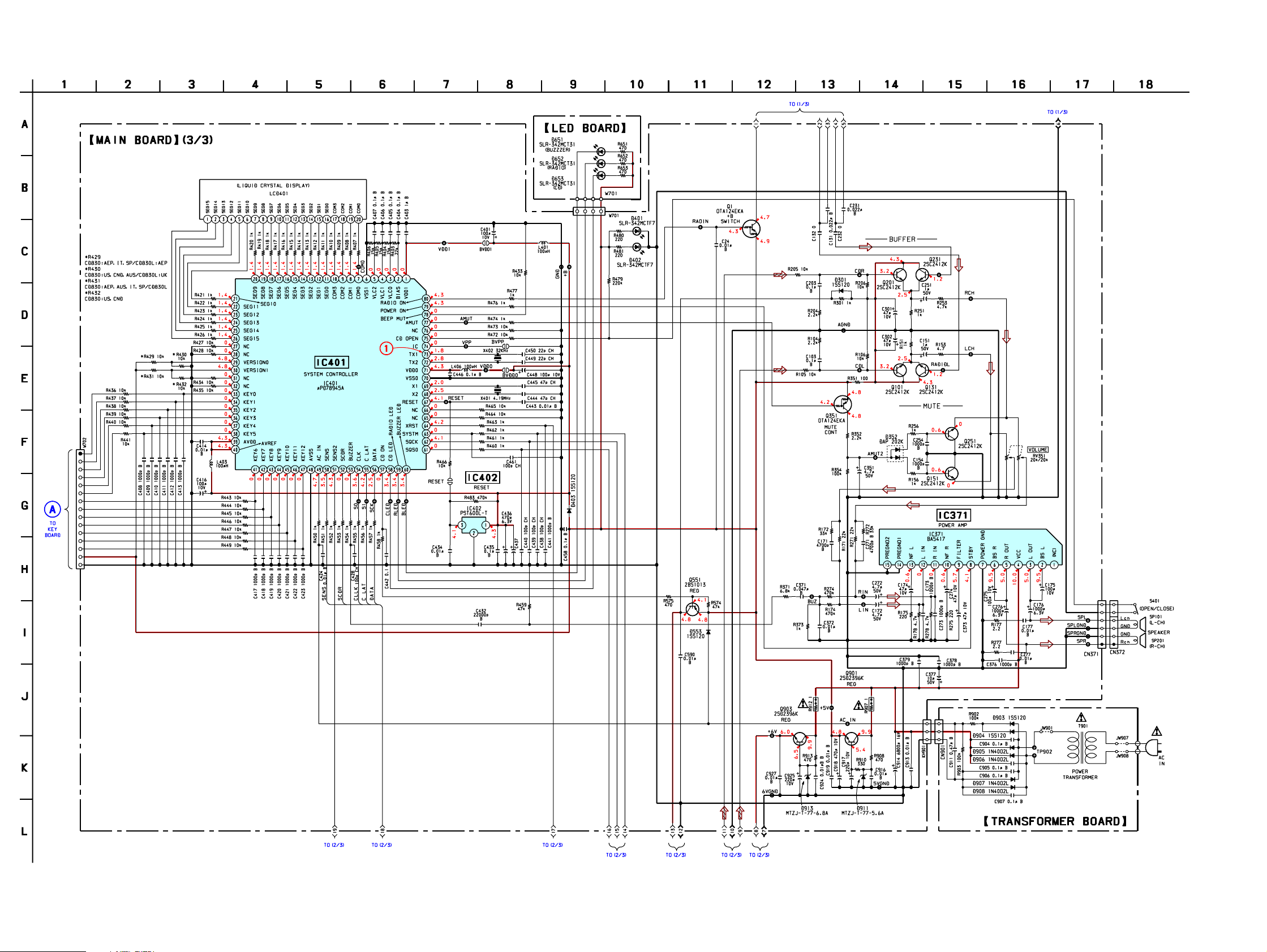
ICF-CD830/CD830L
5-7. SCHEMATIC DIAGRAM – POWER SECTION –
• Refer to page 10 for Waveforms. • Refer to page 22 for IC Pin Function Description.
(Page 19)
1616
ICF-CD830/CD830L
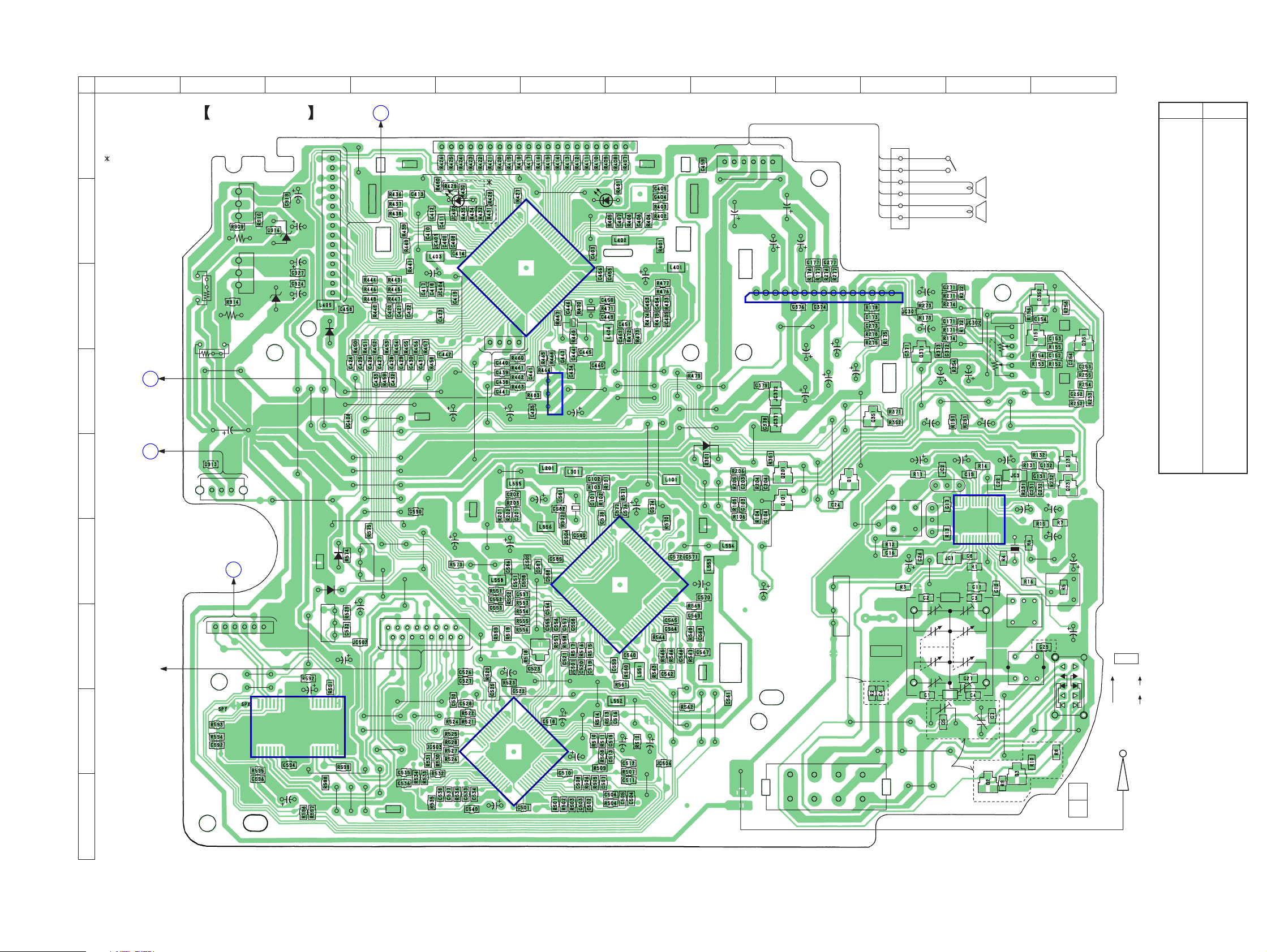
5-8. PRINTED WIRING BOARD – MAIN SECTION –
12
3 4 5 6 7 8 9 101112
MAIN BOARD
A
1
R429:
CD830:AEP,IT,SP/CD830L:AEP
R430:
CD830:US,CND,AUS/CD830L:UK
R431:
CD830:AEP,AUS,IT,SP/CD830L
B
R432:
CD830:US,CND
C
D
E
D
TO
LED
BOARD
C
TO
TRANSFORMER
BOARD
F
G
TO
OPTICAL PICK-UP
BLOCK (KSS-213C)
H
I
R908
R907
R912
MOTOR (6P)
1
Q901
E
Q903
E
D913
R913
C914
KH901
TO
BOARD
B
6
CN591
14
15 28
D911
C591
C595
W702
1
C918
C917
C926
16
C925
D553
D551
Q501
E
IC591
D403
1
• Refer to page 10 for Circuit Board Location.
TO
A
KEY
E
C593
C531
BOARD
1
D401
Q551
CN501
16
15
LCD401 (LIQUID CRYSTAL DISPLAY)
1
21
40
C416
41
C437 C436
C589
2
1
39
40
W701
C539
C579
C529
IC501
52
IC401
2627
1
20
6160
C583
X401
1
3
IC402
C517
14
13
80
X551
80
1
C509
• Semiconductor
Location
Ref. No. Location
D301 E-8
S401
20
D402
1
X402
C448
IC551
20 21
C514
C401
D301
C575
6061
41
40
C524
C563
CN371
16
C176
C276
C175
C275
115
IC371
C274
C375
C174
C373
C377
E
E
E
C301
BPF1
CN372
E
3
1
CV1
TUNING
CD830L
L1
(OPEN/CLOSE)
6
1
C272
C172
E
C351
C302
C20 C21
T1
C9
CT1
C18
CF3
15
16 30
CT2
CV1-2
CV1-3
CV1-1 CV1-4
CT5
CD830L
SP101
(L-CH)
(R-CH)
SP201
RV351
VOLUME
C251C151
CF2
IC1
CT3
CT4
CT6
E
1-680-415-
SPEAKER
C23
1
CF1
L3
CD830:US,CND
L4
E
E
E
E
C15
E
C14
C13
RV1
C12
S1
S1
BAND
AM
FM
(CD830)
(CD830L)
ANT1
(FM ANTENNA)
11
(11)
D352 C-12
D401 B-5
D402 B-6
D403 C-3
D551 F-3
D553 F-3
D911 B-3
D913 C-3
IC1 F-11
IC371 C-9
IC401 C-6
IC402 D-6
IC501 H-5
IC551 F-7
IC591 H-3
Q1 E-9
Q2 I-11
Q3 I-11
Q101 E-9
Q131 E-12
Q151 C-12
Q201 E-9
Q231 E-12
Q251 C-12
Q351 D-10
Q501 G-3
Q551 F-4
Q901 B-2
Q903 C-2
LW
MW
FM
1717
 Loading...