

Sony HCDGV-8 Service manual
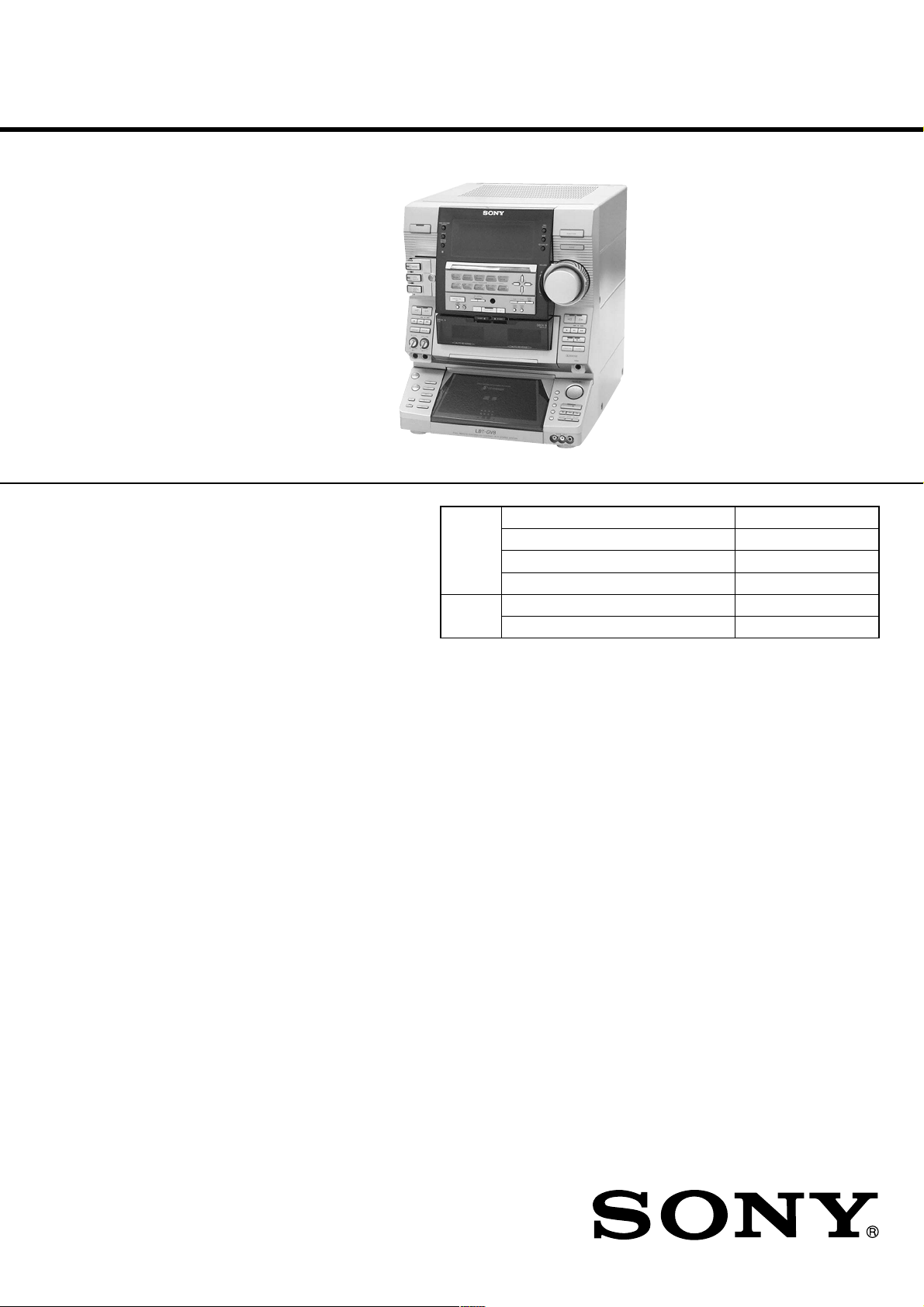
HCD-GV6/GV8
SERVICE MANUAL
Ver 1.0 2001.04
HCD-GV6/GV8 are the amplifier, CD
player, tape deck and tuner section in
LBT-GV6/GV8.
Dolby noise reduction manufactured under license
from Dolby Laboratories Licensing Corporation.
“DOLBY” and the double-D symbol ; are trademarks of Dolby Laboratories Licensing Corporation.
Photo: HCD-GV8
CD
Section
TAPE
Section
E Model
Model Name Using Similar Mechanism HCD-XG60
CD Mechanism Type CDM37L-5BD34L
Base Unit Name BU-5BD34L
Optical Pick-up Name KSS-213DH
Model Name Using Similar Mechanism HCD-XG60
Tape T r ansport Mechanism Type TCM-230PWR42
Amplifier section
HCD-GV8
The following measured at AC 120/220/240V,
50 Hz
DIN power output (rated) 240 + 240 watts
Continuous RMS power output (reference)
HCD-GV6
The following measured at AC 120/220/240V,
50 Hz
DIN power output (rated) 150 + 150 watts
Continuous RMS power output (reference)
Inputs
PHONO IN:
(phono jacks) sensitivity 3 mV,
MIC1/2:
(phone jack) sensitivity 1 mV,
VIDEO IN:
(phono jack) sensitivity 250 mV,
GAME IN:
(phono jack) sensitivity 250 mV,
MD IN:
(phono jack) sensitivity 450 mV,
(4 ohms at 1 kHz, DIN)
320 + 320 watts
(4 ohms at 1 kHz, 10% THD)
(6 ohms at 1 kHz, DIN)
200 + 200 watts
(6 ohms at 1 kHz, 10% THD)
impedance 47 kilohms
impedance 10 kilohms
impedance 47 kilohms
impedance 47 kilohms
impedance 47 kilohms
SPECIFICATIONS
Outputs
PHONES:
(stereo phone jack) accepts headphones of 8
VIDEO OUT:
(phono jack) voltage 250 mV
MD OUT:
(phono jacks) voltage 250 mV
FRONT SPEAKER:
HCD-GV8: accepts impedance of 4 to
HCD-GV6:
Video section
Inputs
VIDEO IN (phono jack): 1 V p-p, 75 ohms
GAME IN (phono jack): 1 V p-p, 75 ohms
Outputs
VIDEO OUT (phono jack):1 V p-p, 75 ohms
S-VIDEO OUT (4-pin/mini-DIN jack):
ohms or more
impedance 1 kilohm
impedance 1 kilohm
16 ohms
accepts impedance of 6 to
16 ohms
Y: 1 V p-p, unbalanced,
Sync negative,
C: 0.286 V p-p,
load impedance 75 ohms
COMPACT DISC DECK RECEIVER
VIDEO CD/CD player section
System Compact disc and digital
Laser Semiconductor laser
Wavelength: 780-790 nm
Frequency response 2 Hz – 20 kHz (±0.5 dB)
Signal-to-noise ratio More than 90 dB
Dynamic range More than 90 dB
Video color system format
CD OPTICAL DIGITAL OUT
(Square optical connector jack, rear panel)
Wavelength: 660 nm
Output level –18 dBm
Tape player section
Recording system 4-track 2-channel stereo
Frequency response 40 – 13,000 Hz (±3 dB),
(DOLBY NR OFF)
audio system
(λ=780nm), Emission
duration: continuous
NTSC, PAL
using Sony TYPE I cassette
40 – 14,000 Hz (±3 dB),
using Sony TYPE II cassette
– Continued on next page –
9-873-826-11 Sony Corporation
2001D0500-1 Home Audio Company
C 2001.4 Shinagawa Tec Service Manual Production Group
HCD-GV6/GV8
Tuner section
FM stereo, FM/AM superheterodyne tuner
FM tuner section
Tuning range 87.5 – 108.0 MHz
Antenna FM lead antenna
Antenna terminals 75 ohm unbalanced
Intermediate frequency 10.7 MHz
AM tuner section
Tuning range
Middle Eastern and Philippine models:
Other models: 531 – 1,602 kHz
Antenna AM loop antenna
Antenna terminals
Intermediate frequency 450 kHz
General
Power requirements 120 V, 220 V or 230 – 240
Power consumption
HCD-GV8 300 watts
HCD-GV6 180 watts
Dimensions (w/h/d) Approx. 355 × 425 × 450
Mass :
HCD-GV8 Approx. 16.0 kg
HCD-GV6 Approx. 15.5 kg
(50 kHz step)
531 – 1,602 kHz
(with the interval set at 9
kHz)
(with the interval set at 9
kHz)
530 – 1,710 kHz
(with the interval set at 10
kHz)
External antenna terminal
V AC, 50/60 Hz
Adjustable with voltage
selector
mm
Notes on chip component replacement
• Never reuse a disconnected chip component.
• Notice that the minus side of a tantalum capacitor may be dam-
aged by heat.
Flexible Circuit Board Repairing
• Keep the temperature of the soldering iron around 270 ˚C during repairing.
• Do not touch the soldering iron on the same conductor of the
circuit board (within 3 times).
• Be careful not to apply force on the conductor when soldering
or unsoldering.
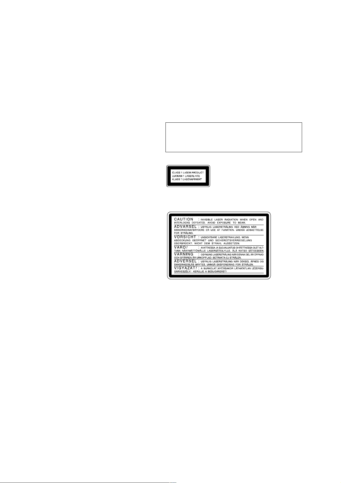
CAUTION
Use of controls or adjustments or performance of procedures
other than those specified herein may result in hazardous radiation exposure.
This appliance is classified as
a CLASS 1 LASER product.
The CLASS 1 LASER
PRODUCT MARKING is
located on the rear exterior.
The following caution label is located inside the unit.
Design and specifications are subject to change
without notice.
SAFETY-RELATED COMPONENT WARNING!!
COMPONENTS IDENTIFIED BY MARK 0 OR DOTTED
LINE WITH MARK 0 ON THE SCHEMATIC DIAGRAMS
AND IN THE PARTS LIST ARE CRITICAL TO SAFE
OPERATION. REPLACE THESE COMPONENTS WITH
SONY PARTS WHOSE PART NUMBERS APPEAR AS
SHOWN IN THIS MANUAL OR IN SUPPLEMENTS PUBLISHED BY SONY.
2

TABLE OF CONTENTS
HCD-GV6/GV8
1. SERVICING NOTES ................................................ 4
2. GENERAL
Location of Controls ....................................................... 5
Setting the Time .............................................................. 6
3. DISASSEMBLY
3-1. Disassembly Flow ........................................................... 7
3-2. Case ................................................................................. 7
3-3. Front Panel Section ......................................................... 8
3-4. Cover (TC), Tape Mechanism Deck
(TCM-230PWR42) ......................................................... 8
3-5. MAIN Board, Fan, D.C. (M901) .................................... 9
3-6. CD Mechanism Deck (CDM37L-5BD34L)................... 10
3-7. Base Unit (BU-5BD34L) ................................................ 11
3-8. Disc Table ........................................................................ 11
4. TEST MODE.............................................................. 12
5. MECHANICAL ADJUSTMENTS....................... 14
6. ELECTRICAL ADJUSTMENTS
Deck section .................................................................... 14
CD Section ...................................................................... 17
Video Section .................................................................. 17
7. DIAGRAMS
7-1. Block Diagram – CD SERVO Section – ....................... 18
7-2. Block Diagram – AUDIO/VIDEO CD Section –.......... 19
7-3. Block Diagram – TUNER/TAPE DECK Section – ...... 20
7-4. Block Diagram – MAIN Section – ................................ 21
7-5. Block Diagram – DISPLAY/KEY CONTROL/
POWER SUPPLY Section – ........................................... 22
7-6. Note for Printed Wiring Boards and
Schematic Diagrams ....................................................... 23
7-7. Printed Wiring Board – BD Board – ............................. 24
7-8. Schematic Diagram – BD Board – ................................ 25
7-9. Schematic Diagram – VIDEO Board (1/2) – ................ 26
7-10. Schematic Diagram – VIDEO Board (2/2) – ................ 27
7-11. Printed Wiring Board – VIDEO Board –....................... 28
7-12. Printed Wiring Boards – CD MOTOR Section – .......... 30
7-13. Schematic Diagram – CD MOTOR Section – .............. 31
7-14. Printed Wiring Board – A UDIO Board – ...................... 32
7-15. Schematic Diagram – AUDIO Board – ......................... 33
7-16. Printed Wiring Board – LEAF SW Board – .................. 34
7-17. Schematic Diagram – LEAF SW Board –..................... 34
7-18. Schematic Diagram – MAIN Board (1/3) – .................. 35
7-19. Schematic Diagram – MAIN Board (2/3) – .................. 36
7-20. Schematic Diagram – MAIN Board (3/3) – .................. 37
7-21. Printed Wiring Board – MAIN Board – ........................ 38
7-22. Printed Wiring Board – PA Board – .............................. 40
7-23. Schematic Diagram – PA Board – ................................. 41
7-24. Printed Wiring Boards – MIC/FRONT INPUT/
HEADPHONES Boards –............................................... 42
7-25. Schematic Diagram – MIC/FRONT INPUT/
HEADPHONES Boards – ............................................. 43
7-26. Printed Wiring Board – PANEL FL Board –................. 44
7-27. Schematic Diagram – PANEL FL Board – ................... 45
7-28. Printed Wiring Boards
– PANEL VR/ILLUMINATION Boards –..................... 46
7-29. Schematic Diagram
– PANEL VR/ILLUMINATION Boards –..................... 47
7-30. Printed Wiring Boards – TC-A/TC-B/CD-L/
CD-R (1)/CD-R (2) Boards – ......................................... 48
7-31. Schematic Diagram – TC-A/TC-B/CD-L/
CD-R (1)/CD-R (2) Boards – ......................................... 49
7-32. Printed Wiring Board – TRANSFORMER Section–.... 50
7-33. Schematic Diagram – TRANSFORMER Section–....... 50
7-34. IC Pin Function Description ........................................... 56
8. EXPLODED VIEWS
8-1. Case, Back Panel Section................................................ 66
8-2. Front Panel Section-1...................................................... 67
8-3. Front Panel Section-2...................................................... 68
8-4. Chassis Section ............................................................... 69
8-5. CD Mechanism Deck Section (CDM37L-5BD34L)...... 70
8-6. Base Unit Section (BU-5BD34L)................................... 71
8-7. Tape Mechanism Deck Section-1
(TCM-230PWR42) ......................................................... 72
8-8. Tape Mechanism Deck Section-2
(TCM-230PWR42) ......................................................... 73
9. ELECTRICAL PARTS LIST ............................... 74
3
HCD-GV6/GV8
SECTION 1
SERVICING NOTES
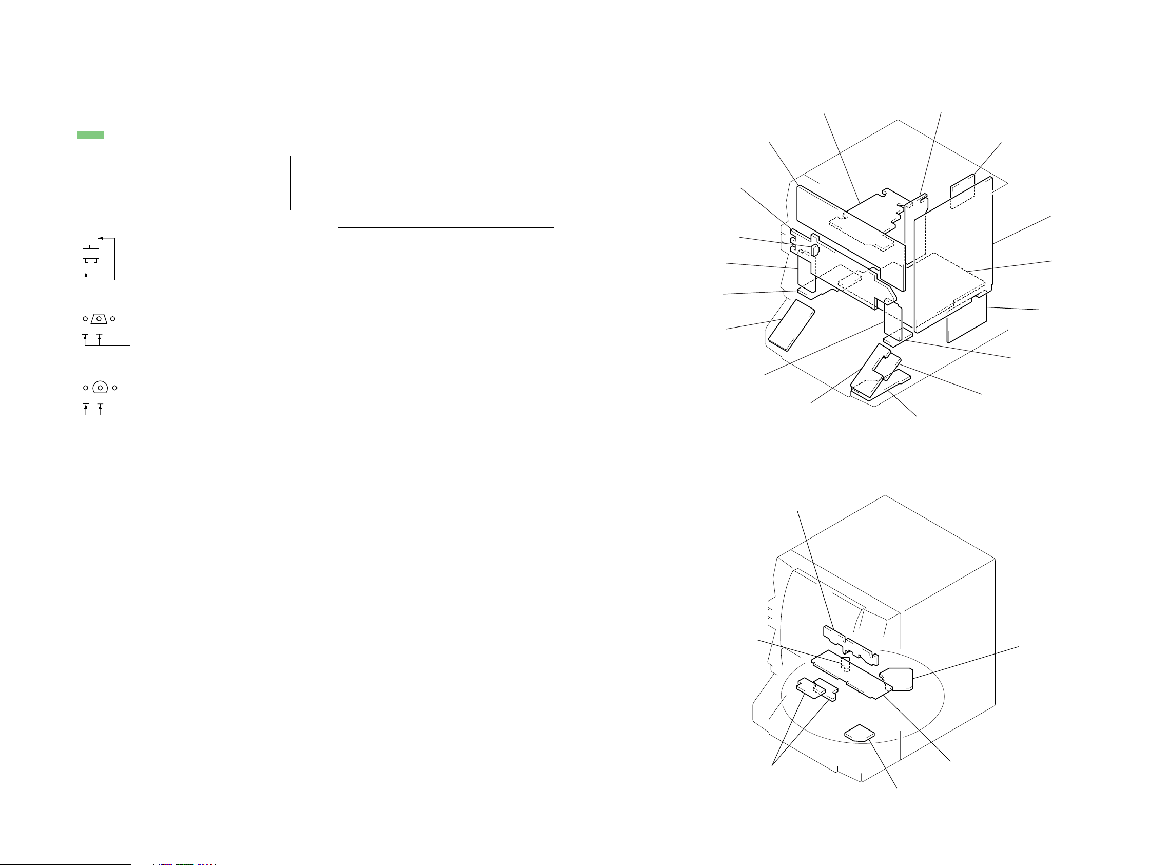
NOTES ON HANDLING THE OPTICAL PICK-UP
BLOCK OR BASE UNIT
The laser diode in the optical pick-up block may suffer electrostatic break-down because of the potential difference generated
by the charged electrostatic load, etc. on clothing and the human
body.
During repair, pay attention to electrostatic break-down and also
use the procedure in the printed matter which is included in the
repair parts.
The flexible board is easily damaged and should be handled with
care.
NOTES ON LASER DIODE EMISSION CHECK
The laser beam on this model is concentrated so as to be focused
on the disc reflective surface by the objective lens in the optical
pick-up block. Therefore, when checking the laser diode emission, observe from more than 30 cm away from the objectiv e lens.
LASER DIODE AND FOCUS SEARCH OPERATION
CHECK
Carry out the “S curve check” in “CD section adjustment” and
check that the S curve waveforms is output three times.
• MODEL IDENTIFICATION
– Rear Panel –
SELF-DIAGNOSIS
This unit is equipped with a self-diagnosis function.
The function is used for diagnosing the conditions of the circuits
of the VIDEO board.
The circuits can be determined if normal or abnormal by the lighting of D502 of the VIDEO board.
Lighting of D502
When lit : Operates normally
Blinks repeatedly : The circuit may be faulty.
– VIDEO Board (Side A) –
IC505
PART No.
MODEL PART No.
HCD-GV6: Malaysia and
Singapore models
HCD-GV6: Saudi Arabia model 4-232-090-1
HCD-GV8: Malaysia and
Singapore models
HCD-GV6: Indonesia model 4-232-090-6
4-232-090-0
4-232-090-2
D502
[]
[]
[]
[]
4
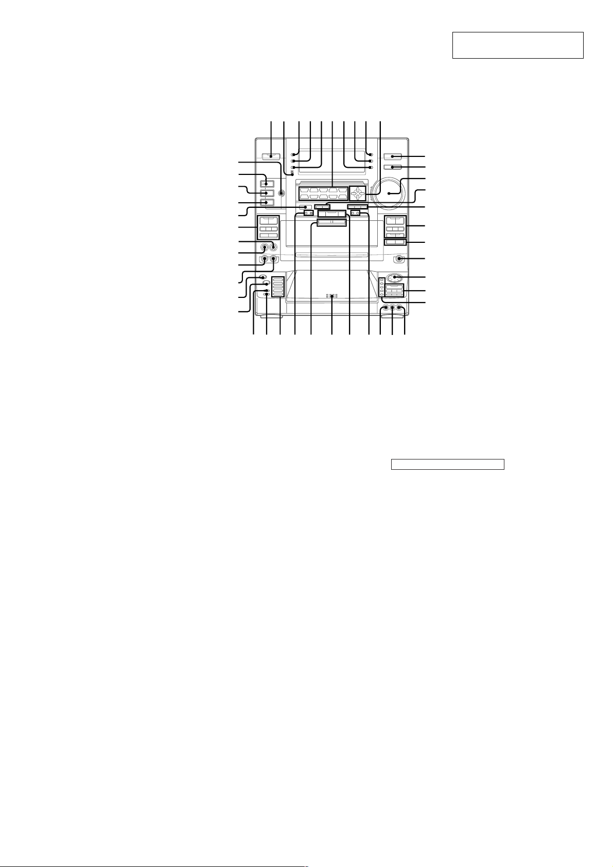
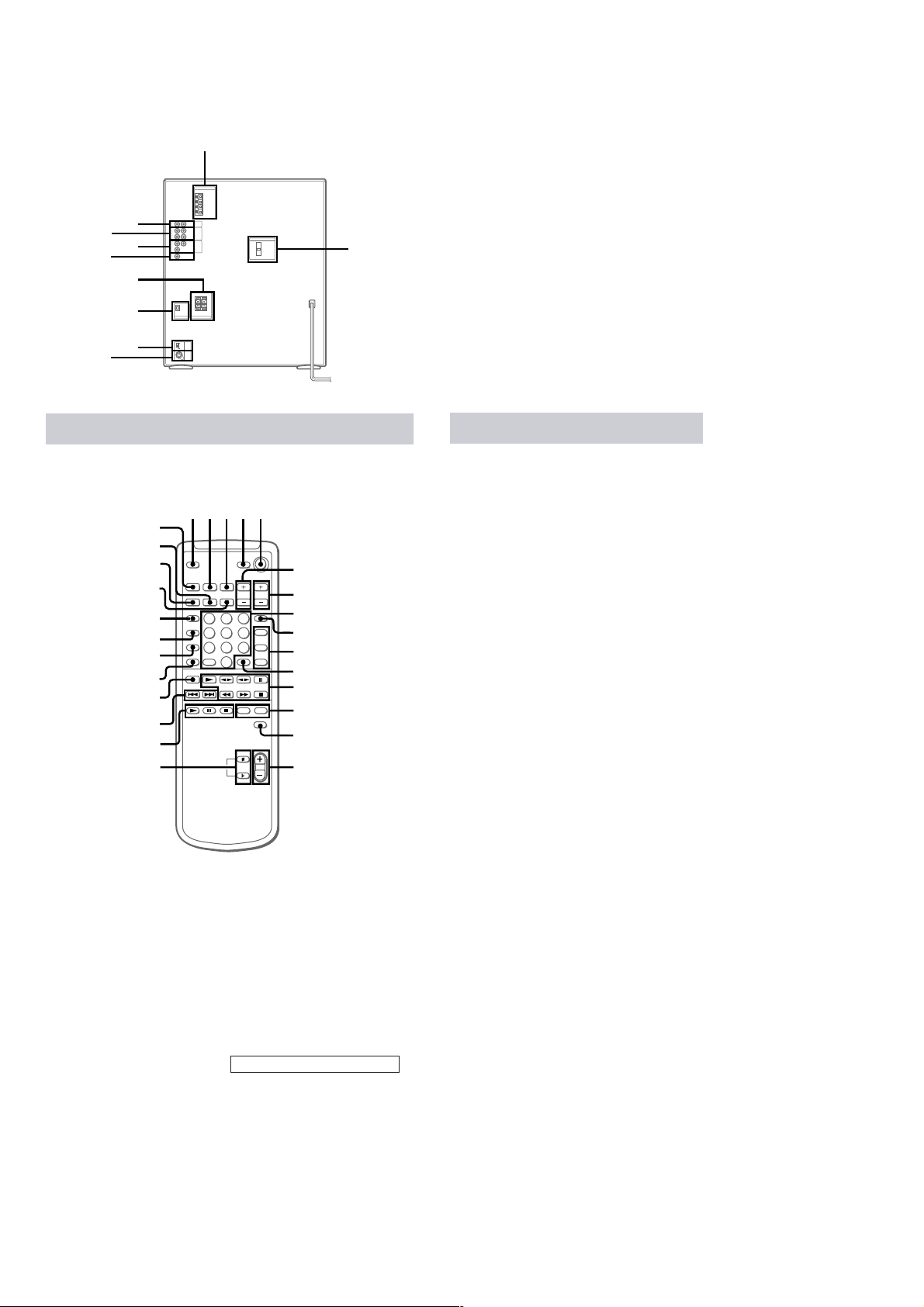
LOCATION OF CONTROLS
– Front Panel –
SECTION 2
GENERAL
1
2
3456789
HCD-GV6/GV8
This section is extracted from
instruction manual.
q;
rf
rd
rs
ra
r;
el
ek
ej
eh
eg
ef
ed
es
ACTIVE wa (19)
A EJECT Z/Z B EJECT wk (22)
AUDIO L jack wd (31)
AUDIO R jack ws (31)
CD FLASH ed (14)
CD LOOP ef (7,14)
CD SYNC qj (23,24)
DIRECT EQUALIZER 6 (26)
SALSA REGGAE
SAMBA TANGO
MOVIE POP
ROCK JAZZ
DANCE GAME
DIRECTION el (22,23,24,29)
DISC SKIP w; (9~13,18,24)
DISC 1~5 e; (10,12)
DISPLA Y 4 (8,14)
DOLBY NR el (22,23)
ECHO LEVEL ek (28)
EDIT es (24)
ENTER wl (20)
ENTER/NEXT qg (8,25,27,30,36 )
FLAT qg (26)
FUNCTIONqa
(7,12,13,23,24,29,31,32)
ea
e;
GAME qs (29,31)
GROOVE rd (26)
H SPEED DUB qj (23)
IR receptor 2
Jog dial (AMS./>) ql
(10~14,18,24)
KARAOKE PON/MPX r; (28)
KEY CONTROL 2/# qf (28)
MIC 1 jack eh (28)
MIC 2 jack eg (28)
MIC LEVEL ej (28)
NEXT wa (10,11,17,18)
NON STOP ea (13)
P.FILE qg (26,27)
PHONES jack qk
PLAY MODE w; ( 9,12,13,18,24)
POWER SAVE/DEMO
(STANDBY) 3 (8)
PREV wa (10,11,17,18)
PUSH OPEN wj (9,10,12)
REPEAT w; (10,12)
RETURN wa (11)
SELECT wa (11)
SLEEP 8 (29)
SPECTRUM ANALYZER 5 (28)
STEREO/MONO wg (21)
wh
qa
qs
qd
qf
qg
qh
qj
qk
ql
w;
wa
wswdwfwgwjwkwl
SUPER WOOFER rs ( 26,32)
SUPER WOOFER MODE ra (26)
SURROUND rf(23,26)
TIMER SELECT 9 (25,30)
TUNER/BAND wh(20,21,23)
TUNER MEMORY wl (20)
TUNING MODE wg (20,21)
VIDEO jack wf (31)
VOLUME control qd (21)
BUTTON DESCRIPTIONS
@/1 1
c/CLOCK SET 7
v/V/b/B q;
z REC qh
X qh
m /M, AMS./>
(TAPE A/B) qhel
h/H qhel
x qhw;el
m /M (CD/VCD) w;
HX w;
+/– wh
5
HCD-GV6/GV8
– Rear Panel –
2
3
4
5
6
7
8
9
1
0
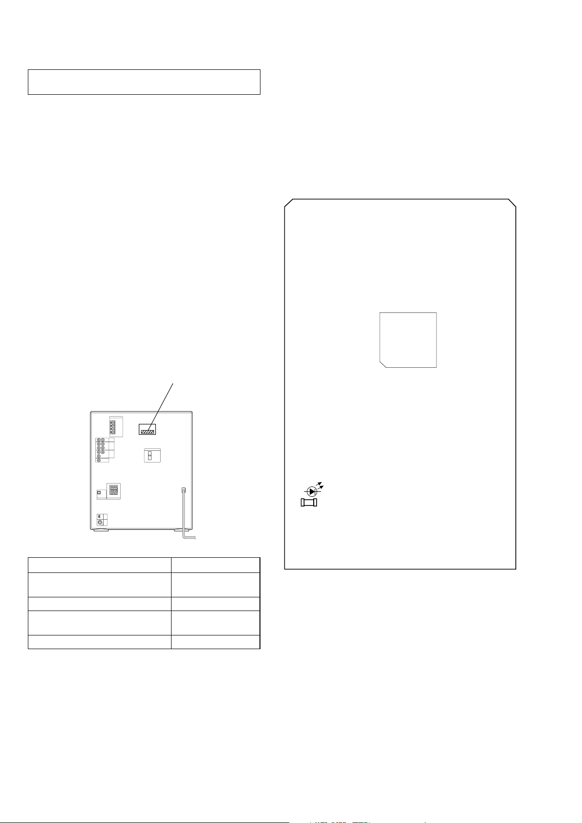
1 ANTENNA terminal
2 PHONO IN jack
3 MD IN/OUT jack
4 VIDEO/AUDIO IN jack
5 VIDEO OUT jack
6 FRONT SPEAKER terminal
7 CD DIGITAL OUT OPTICAL terminal
8 SYSTEM SELECT switch
9 S VIDEO OUT jack
0 VOLTAGE SELECTOR switch
Remote control
wj
wh
wg
wf
wd
ws
wa
w;
ql
qk
qj
qh
1
234
5
6
7
8
9
q;
qa
qs
qd
qf
qg
Setting the time
1 Turn on the system.
Press c/CLOCK SET.
2
When you set the time for the first time,
skip to step 5.
3 Press v/V repeatedly to select “SET
CLOCK.”
4 Press ENTER/NEXT.
5 Press v/V repeatedly to set the hour.
6 Press ENTER/NEXT.
The minute indication flashes.
7 Press v/V repeatedly to set the minute.
8 Press ENTER/NEXT.
The clock starts working.
Tip
If you’ve made a mistake or want to change the time,
start over from step 2.
Note
The clock settings are canceled when you disconnect
the power cord or if a power failure occurs.
ACTIVE wa (19)
CHECK wh (13)
CLEAR wf (13,17)
DECK A nN qs (22)
DECK B nN qs (22)
DISPLAY 2 (8,14)
D.SKIP wg (9~13,17,18,24)
EDIT ws (24)
FILE SELECT ON/OFF q; (26)
FILE SELECT v/V q; (14)
FLASH qd (14)
FUNCTION w;
(7,12,13,23,24,29,31,32)
KEY CONTROL
LOOP qd (14)
MD N qj
MD X qj
MD x qj
NEXT, +, > qk
(10,11,12,17,18,21,22)
Numeric buttons 8 (10,11,16~18)
ON SCREEN 3 (15,16)
PREV, –, . qk
(10,11,12,17,18,21,22)
REPEAT wd (10,12)
2/# qh (28)
6
SELECT CD N qs
(9,10,12,16~18)
SLEEP wj (29)
SPECIAL MENU 9 (16~18)
SURROUND qf (23,26)
TUNER/BAND ql(20,21,23)
TV CH +/– 7 (8)
TV/VIDEO 1 (8)
TV VOL +/– 6 (8)
TV @/1 4 (8)
VOL +/– qg (21)
BUTTON DESCRIPTIONS
@/1 5
O RETURN qa
x qs
m/M qs
X qs
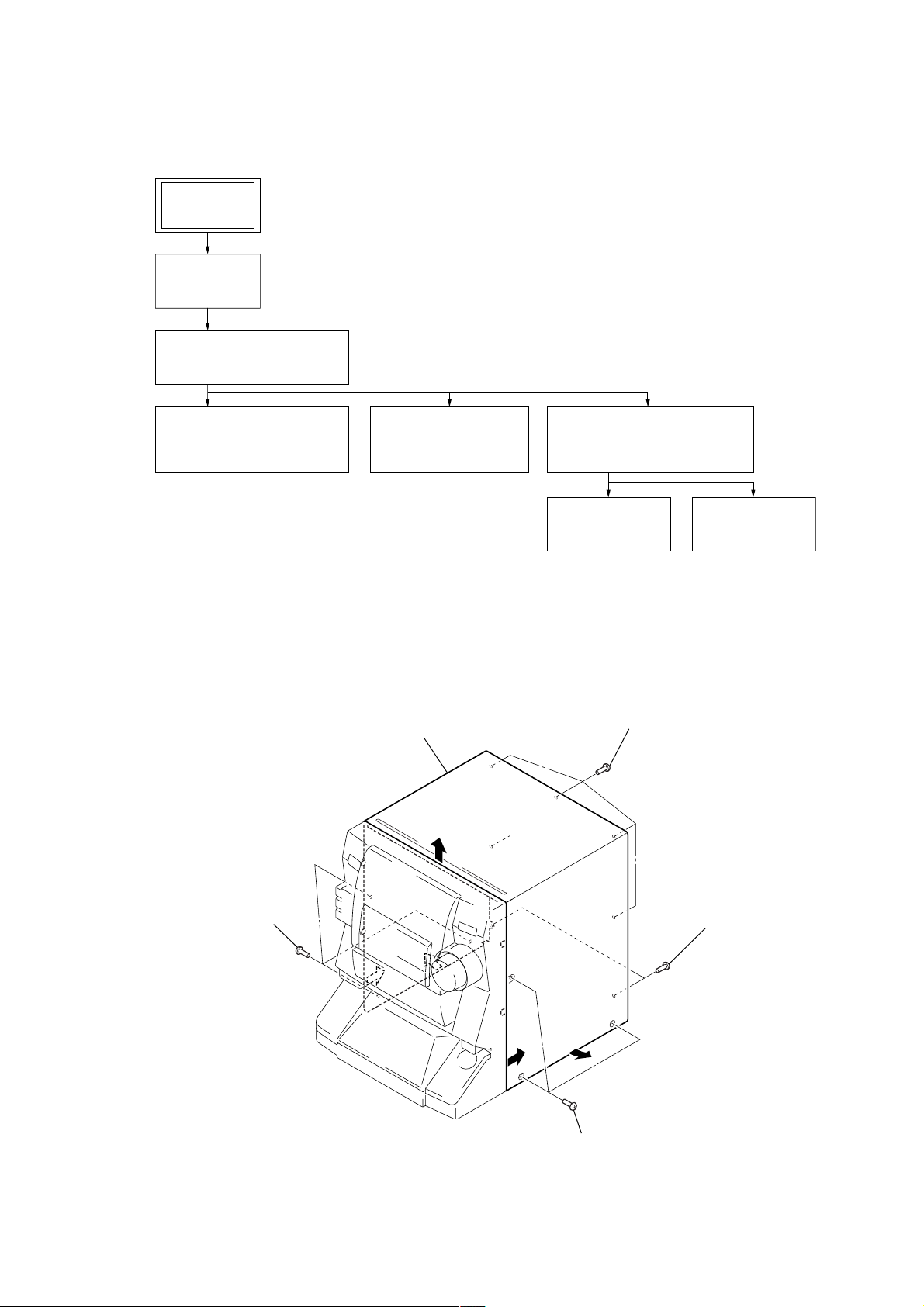
• This set can be disassembled in the order shown below.
)
3-1. DISASSEMBLY FLOW
SET
3-2. CASE
(Page 7)
3-3. FRONT PANEL SECTION
(Page 8)
HCD-GV6/GV8
SECTION 3
DISASSEMBLY
3-4. COVER (TC),
TAPE MECHANISM DECK
(TCM-230PWR42)
(Page 8)
Note: Follow the disassembly procedure in the numerical order given.
3-5. MAIN BOARD,
FAN, D.C. (M901)
(Page 9)
3-2. CASE
6
case
3-6. CD MECHANISM DECK
(CDM37L-5BD34L)
(Page 10)
3-7. BASE UNIT
(BU-5BD34L)
(Page 11)
2
five screws
(BVTT3
3-8. DISC T ABLE
×
6)
(Page 11)
1
three screws
(CASE3 TP2)
5
4
5
4
1
three screws
(CASE3 TP2)
3
two screws
(BVTP3
×
8
7
HCD-GV6/GV8
)
)
3-3. FRONT PANEL SECTION
1
1
4
3
lug
two screws
(BVTP3
×
8)
1
wire (flat type)
(15 core) (CN303)
wire (flat type)
(17 core) (CN304)
wire (flat type)
(13 core) (CN431)
2
two connectors
(CN452, 702)
3
4
screw
(BVTP3
two lugs
×
8
6
7
front panel section
5
four screws
(BVTP3
×
claw
8)
3-4. COVER (TC), TAPE MECHANISM DECK (TCM-230PWR42)
4
two screws
(BVTP3
×
8)
5
screw
(BVTP3
×
8)
3
wire (flat type) (17 core)
(CN1001)
3
2
connector
(CN806)
wire (flat type) (15 core
(CN601)
4
two screws
(BVTP3
×
8)
1
five claws
5
tape mechanism deck
(TCM-230PWR42)
2
cover (TC)
8
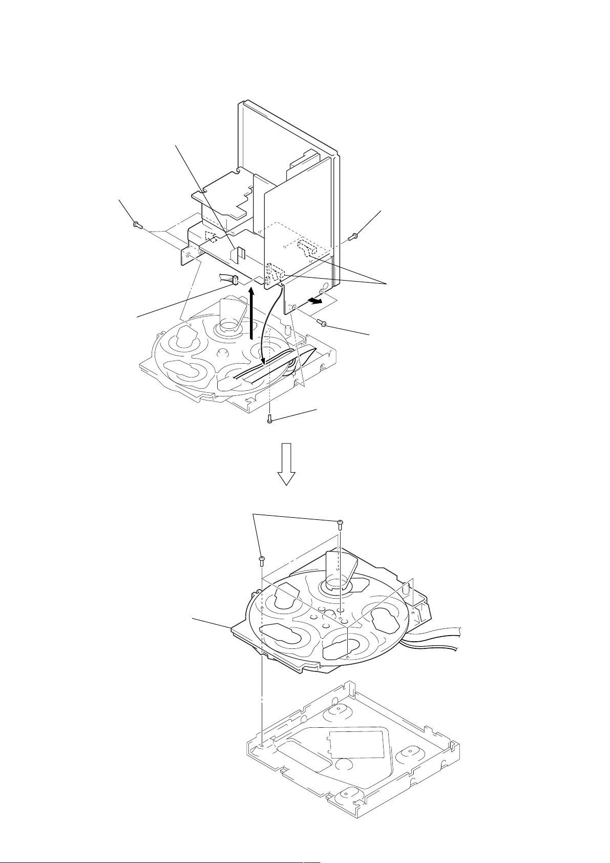
3-5. MAIN BOARD, FAN, D.C. (M901)
)
8
back panel
9
wire (flat type) (19 core)
(CN411)
7
1
fan, D.C.
(M901)
wire (flat type)
(13 core) (CN441)
2
4
eight screws
(BVTP3
×
8)
2
2
6
2
three screws
(BVTP3
3
three screws
(BVTP3
HCD-GV6/GV8
screw
(BVTP3
three screws
(BVTP3
two screws
(BVTP3
×
8)
×
8)
×
8)
×
8)
×
8)
0
connector
(CN412)
qa
qs
two connectors
(CN901, 902)
connector (CN903
5
qd
MAIN board
two screws
×
(BVTP3
8)
9
HCD-GV6/GV8
3-6. CD MECHANISM DECK (CDM37L-5BD34L)
wire (flat type)
1
(19 core) (CN411)
4
three screws
(BVTP3
2
×
connector
(CN412)
8)
6
7
6
3
8
4
two screws
(BVTP3
three screws
(BVTP3
×
8)
Open the cable clamp.
×
8)
0
CD mechanism deck
(CDM37L-5BD34L)
9
five screws
(BVTP3 × 8)
5
two screws
(BVTP3
×
8)
10
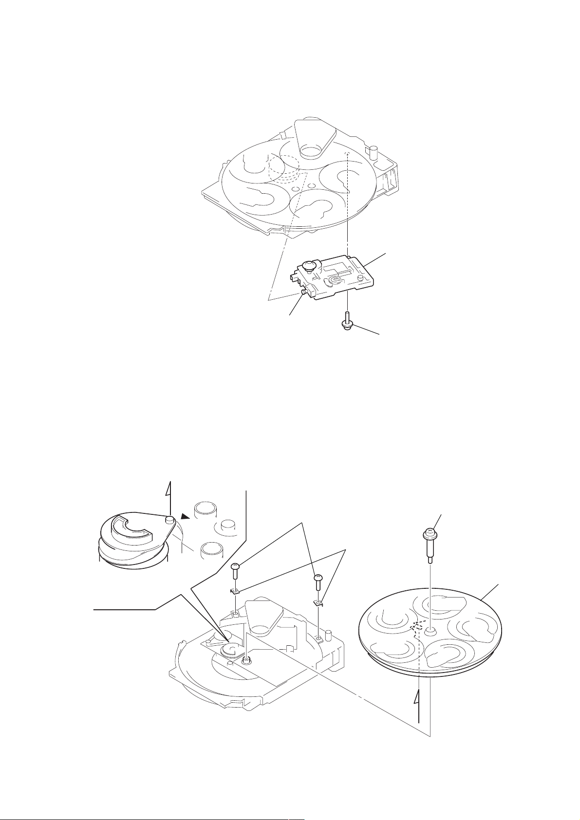
3-7. BASE UNIT (BU-5BD34L)
w
1 two screws
(BVTP3 × 8)
A
2 two brackets (BU)
3 step screw
4 disc table
A
3
base unit (BU-5BD34L)
HCD-GV6/GV8
2
3-8. DISC TABLE
Note: When the disc table is installed, adjust the positions of roller cam
and mark B as shown in the figure, then set to the groove of disc
table.
boss
1
BU fitting scre
11

HCD-GV6/GV8
SECTION 4
TEST MODE
[MC Cold Reset]
• The cold reset clears all data including preset data stored in the
RAM to initial conditions. Execute this mode when returning
the set to the customer.
Procedure:
1. Turn the power ON or set to the DEMO mode.
2. Press three buttons of [ /CLOCK SET], [ENTER/NEXT], and
?/1 simultaneously.
3. The set is reset, and displays “COLD RESET”, then becomes
DEMO mode.
[MC Hot Reset]
• This mode resets the set with the preset data kept stored in the
memory. The hot reset mode functions same as if the power
cord is plugged in and out.
Procedure:
1. Turn the power ON or set to the DEMO mode.
2. Press three buttons of [ /CLOCK SET], [ENTER/NEXT],
and [DISC 1] simultaneously.
3. The set is reset, and becomes standby state.
[Change-over the AM Tuning Interval]
(EXCEPT Saudi Arabia model)
• The AM tuning interval can be changed over 9 kHz or 10 kHz.
Procedure:
1. Press the ?/1 button to turn the power ON.
2. Select the function “TUNER”, and press the [TUNER/BAND]
button to select the BAND “AM”.
3. Press the ?/1 button to turn the power OFF.
4. Press the [ENTER/NEXT] and ?/1 buttons simultaneously,
and the display on the fluorescent indicator tube changes to
“AM 9 K STEP” or “AM 10 K STEP”, and thus the tuning
interval is changed over.
c
c
[CD Delivery Mode]
• This mode moves the optical pick-up to the position durable to
vibration. Use this mode when returning the set to the customer
after repair.
Procedure:
1. Press the ?/1 button to turn the power ON.
2. Press the [LOOP] and ?/1 buttons simultaneously.
3. A message “LOCK” is displayed on the fluorescent indicator
tube, and the CD delivery mode is set.
[LED and Fluorescent Indicator Tube All Lit, Key Check
Mode]
Procedure:
1. Press three buttons of [ /CLOCK SET], [ENTER/NEXT],
and [DISC 2] simultaneously.
2. LEDs and fluorescent indicator tube are all turned on.
Press the [DISC 2] button, and the key check mode is activated.
3. In the key check mode, the fluorescent indicator tube displays
“K 0 J0 V0”. Each time a button is pressed, “K” value increases. However , once a button is pressed, it is no longer tak en
into account.
“J” value increases like 1, 2, 3 ... if turn the JOG dial clockwise, or it decreases like 0, 9, 8 ... if turn the JOG dial counterclockwise.
“V” value increases like 1, 2, 3 ... if turn the [VOLUME] dial
clockwise, or it decreases like 0, 9, 8 ... if turn the JOG dial
counterclockwise.
4. To release from this mode, press three buttons in the same
manner as step 1, or disconnect the power cord.
c
12
HCD-GV6/GV8
[Aging Mode]
This mode can be used for operation check of tape deck section.
Tape deck section work in parallel.
• If an error occurred:
The aging operation stops and display then status.
• If no error occurs:
The aging operation continues repeatedly.
Procedure:
1. Load the tapes into the decks A and B respectively.
2. Press the [FUNCTION] button to select the function “CD”.
3. Press the [PLAY MODE] button to set the “ALL DISCS” mode,
and press the [REPEAT] button to “REPEAT” off.
4. Press three buttons of [ /CLOCK SET], [ENTER/NEXT],
c
and [DISC 4] simultaneously.
5. The aging mode is activated, if the indicator of disc tray num-
ber on the fluorescent indicator tube is blinking.
6. To release from the aging mode, press the ?/1 button to turn
the power OFF and operate the cold reset. (Refer to the “MC
Cold Reset”)
1. Display at the Aging Mode
• Display operating state of tape deck section alternately.
• If an error occurred, stop display.
2. Tape Deck Section
• The sequence during the aging mode is following as below.
• If an error occurred, stop display that step.
Aging mode sequence (Tape deck section) :
Rewind the tape A and B
“TAPE A AG-1”
Shut off
FWD play the tape A
“TAPE A AG-2”
2 minutes
Fast forward the tape A
“TAPE A AG-3”
Shut off or 20 seconds
REV play the tape A
“TAPE A AG-4”
2 minutes
Rewind the tape A
“TAPE A AG-5”
Shut off
FWD play the tape B
“TAPE B AG-2”
2 minutes
Fast forward the tape B
“TAPE B AG-3”
Shut off or 20 seconds
REV play the tape B
“TAPE B AG-4”
2 minutes
Rewind the tape B
“TAPE B AG-5”
Shut off
Note: “TAPE * AG-*” is display of each step.
13
HCD-GV6/GV8
SECTION 5
MECHANICAL ADJUSTMENTS
SECTION 6
ELECTRICAL ADJUSTMENTS
Precaution
1. Clean the following parts with a denatured alcohol-moistened
swab:
record/playback heads pinch rollers
erase head rubber belts
capstan idlers
2. Demagnetize the record/playback head with a head demagnetizer.
3. Do not use a magnetized screwdriver for the adjustments.
4. After the adjustments, apply suitable locking compound to the
parts adjusted.
5. The adjustments should be performed with the rated power supply voltage unless otherwise noted.
Torque Measurement
Mode Torque Meter Meter Reading
FWD CQ-102C (31 to 71 g•cm)
FWD
back tension
REV CQ-102RC (31 to 71 g•cm)
REV
back tension
FF/REW CQ-201B (71 to 143 g•cm)
FWD tension CQ-403A (100 g or more)
REV tension CQ-403A (100 g or more)
CQ-102C (2 to 6 g•cm)
CQ-102RC (2 to 6 g•cm)
3.1 to 6.96 mN•m
(0.43 – 0.98 oz•inch)
0.20 to 0.58 mN•m
(0.03 – 0.08 oz•inch)
3.1 to 6.96 mN•m
(0.43 – 0.98 oz • inch)
0.20 to 0.58 mN•m
(0.03 – 0.08 oz • inch)
6.97 to 14.02 mN•m
(0.99 – 1.99 oz • inch)
9.80 mN•m
(3.53 oz or more)
9.80 mN•m
(3.53 oz or more)
DECK SECTION
0 dB = 0.775 V
Precaution
1. Demagnetize the record/playback head with a head demagnetizer.
2. Do not use a magnetized screwdriver for the adjustments.
3. After the adjustments, apply suitable locking compound to the
parts adjust.
4. The adjustments should be performed with the rated power
supply voltage unless otherwise noted.
5. The adjustments should be performed in the order given in
this service manual. (As a general rule, playback circuit adjustment should be completed before performing recording
circuit adjustment.)
6. The adjustments should be performed for both L-CH and RCH.
7. Switches and controls should be set as follows unless otherwise specified.
8. Set to the DOLBY NR OFF.
9. Set to the test mode.
(1) Press the ?/1 button to turn the power ON.
(2) Select the function “TAPE A or B”.
(3) Press the button of [ /CLOCK SET], [ENTER/NEXT],
c
and [DISC 3] simultaneously , to set the tape deck test mode
and displays “TEST MODE” on the fluorescent indicator
tube.
(4) To release from the test mode, press the ?/1 button.
• Test Tape
Tape Signal Used for
P-4-A100 10 kHz, – 10 dB Azimuth Adjustment
WS-48B 3 kHz, 0 dB Tape Speed Adjustment
P-4-L300 315 Hz, 0 dB Playback Level Adjustment
14
HCD-GV6/GV8
+
–
set
test tape
WS-48B
(3 kHz, 0 dB)
MAIN board
MD OUT jack (J701)
L-CH, R-CH
frequency counter
r
r
Record/Playback Head Azimuth Adjustment
DECK A DECK B
Note: Perform this adjustments for both decks
Procedure:
1. Mode: Playback (FWD)
2. Turn the adjustment screw and check output peaks. If the peaks
test tape
P-4-A100
(10 kHz, – 10 dB)
MAIN board
MD OUT jack (J701)
L-CH, R-CH
set
level mete
+
–
do not match for L-CH and R-CH, turn the adjustment screw
so that outputs match within 1dB of peak.
Output
level
within
1dB
within
1dB
L-CH
peak
Adjustment Location:Playback Head (Deck A).
Record/Playback/Erase Head (Deck B).
forward
reverse
Tape Speed Adjustment DECK B
Mode: Playback
R-CH
Screw
position
peak
L-CH
peak
R-CH
peak
Screw
position
3. Mode: Playback
MAIN board
test tape
P-4-A100
(10 kHz, – 10 dB)
L-CH
set
R-CH
in phase 45 ° 90 ° 135 ° 180°
MD OUT jack (J701)
L-CH
R-CH
waveform of oscilloscope
good
oscilloscope
wrong
H
V
4. Repeat step 1 to 3 in playback (REV) mode.
5. After the adjustments, apply suitable locking compound to the
parts adjusted.
1. Insert the WS-48B into the deck B.
2. Press the H button on the deck B.
3. Press the [H SPEED DUB] button in playback mode.
Then at HIGH speed mode.
4. Adjust RV1001 on the LEAF SW board do that frequency
counter reads 6,000 ± 180 Hz.
5. Press the [H SPEED DUB] button.
Then back to NORMAL speed mode.
6. Adjust RV1002 on the LEAF SW board so that frequency
counter reads 3,000 ± 90 Hz.
Adjustment Location: LEAF SW board
Sample value of Wow and Flutter: 0.3% or less W.RMS (JIS)
(WS-48B)
Playback Level Adjustment DECK A DECK B
Procedure:
Mode: Playback
test tape
P-4-L300
(315 Hz, 0 dB)
set
MAIN board
MD OUT jack (J701)
L-CH
level mete
+
–
Deck A is RV311 (L-CH), Deck B is RV301 (L-CH) so that adjustment within specification values as follows.
Specification Values:
J701 PB level: 301.5 to 338.3 mV (– 8.2 to – 7.2 dB) level
difference between the channels: within ± 0.5 dB
Adjustment Location: AUDIO board
15
HCD-GV6/GV8
r
r
REC Bias Adjustment DECK B
Procedure:
1. Mode: Record
FUNCTION: VIDEO
MAIN board
VIDEO AUDIO IN jack (J701)
L-CH, R-CH
50 mV (– 23.8 dB)
600
Ω
set
blank tape
CN-123
AF OSC
1) 315 Hz
2) 10 kHz
attenuator
2. Mode: Playback
recorded
portion
set
MAIN board
MD OUT jack (J701)
L-CH, R-CH
level mete
+
–
3. Confirm playback the signal recorded in step 1 become specification values as follows.
If these values are out of specification v alues, adjust the R V341
(L-CH) and RV441 (R-CH) on the AUDIO board to repeat
steps 1and 2.
Specification values: Playback output of 315 Hz to playback
output of 10 kHz: ± 0.5 dB
Adjustment Location: AUDIO board
Specification values:
J701 PB level: 47.2 to 53.0 mV (– 24.3 to – 23.3 dB)
Adjustment Location: MAIN board
– MAIN BOARD (Conductor Side) –
VIDEO
AUDIO IN
L/R
J701
REC LEVEL
IC301
RV351
R-CH
MD OUT
RV301
L-CH
L/R
– AUDIO BOARD (Component Side) –
RV441
RV301
PB LEVEL
(L)
– DECK B –
IC602
RV341
RL
REC BIAS
CN601
RV311
PB LEVEL (L)
– DECK A –
REC Level Adjustment DECK B
Procedure:
1. Mode: Record
FUNCTION: VIDEO
MAIN board
VIDEO AUDIO IN jack (J701)
L-CH, R-CH
AF OSC
315 Hz, 50 mV (– 23.8 dB)
600
attenuator
Ω
blank tape
CS-123
set
2. Mode: Playback
recorded
portion
set
MAIN board
MD OUT jack (J701)
L-CH, R-CH
level mete
+
–
3. Confirm playback the signal recorded in step 1 become specification values as follows.
If these values are out of specification v alues, adjust the R V301
(L-CH) and R V351 (R-CH) on the MAIN board to repeat steps
1 and 2.
– LEAF SW BOARD (Component Side) –
TAPE SPEED
(NORMAL) (HIGH)
RV1002
RV1001
CN1001
16
HCD-GV6/GV8
+
–
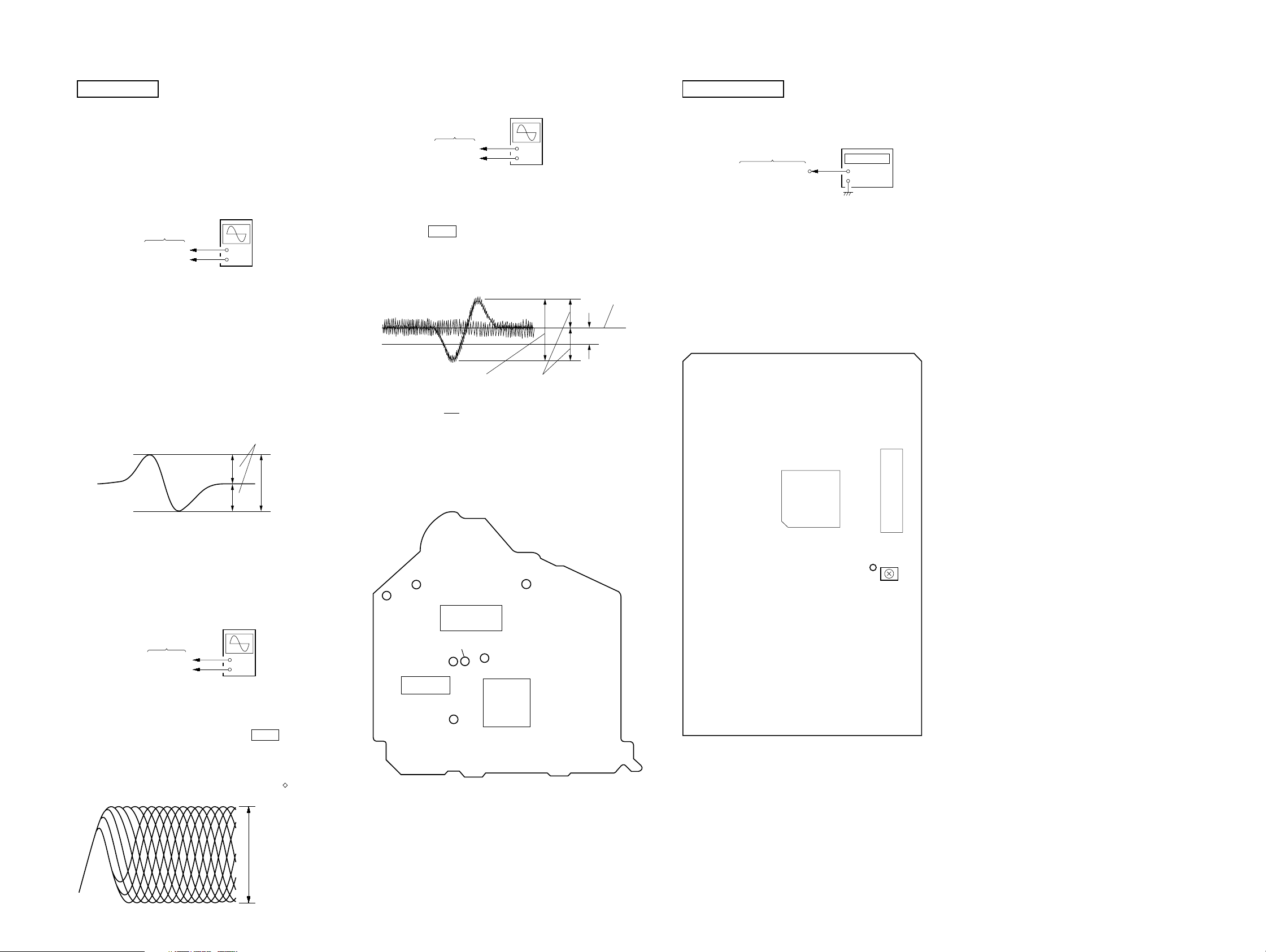
TP508 (27 MHz)
VIDEO board
frequency counter
IC505
IC507
TP508
(27 MHz)
CT503
VIDEO
Frequency
Adjustment
– VIDEO BOARD (Side A) –
e
e
)
CD SECTION
Note:
1. CD Block is basically designed to operate without adjustment. Therefore, check each item in order given.
2. Use YEDS-18 disc (3-702-101-01) unless otherwise indicated.
3. Use an oscilloscope with more than 10 MΩ impedance.
4. Clean the object lens by an applicator with neutral detergent when the
signal level is low than specified value with the following checks.
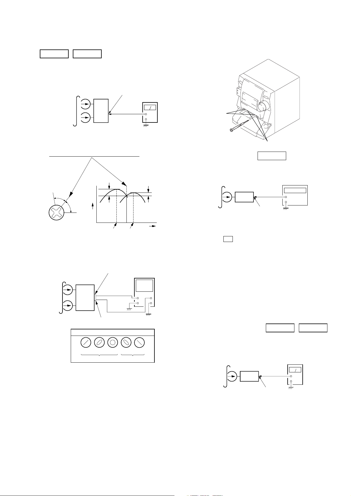
S-Curve Check
oscilloscop
BD board
TP (FE)
TP (VC)
Procedure:
1. Connect oscilloscope to TP (FE) and TP (VC).
2. Connect between TP (FE1) and TP (VC) by lead wire.
3. Connect between TP (AGCCON) and TP (GND) by lead wire.
4. Turn the power ON.
5. Load a disc (YEDS-18) and actuate the focus search. (In con-
sequence of open and close the disc tray, actuate the focus
search)
6. Cofirm that the oscilloscope waveform (S-curve) is symmetri-
cal between A and B. And confirm peak to peak level within
4 ± 1 Vp-p.
S-curve waveform
+
–
symmetry
E-F Balance (1 Track Jump) Check
oscilloscope
(DC range)
BD board
TP (TE)
TP (VC)
+
–
Procedure :
1. Connect oscilloscpe to TP (TE) and TP (VC).
2. Turn the power ON.
3. Load a disc (YEDS-18) and playback the number five track.
4. Press the H X button. (Becomes the 1 track jump mode)
5. Confirm that the level B and A (DC voltage) on the oscilloscope waveform.
1 track jump waveform
B
0V
level = 1.3 ± 0.6 Vp-p symmetry
Specified level: × 100 = less than ± 22%
A
B
center of
waveform
A (DC voltage
6. After check, remove the lead wire connected in step 1.
VIDEO SECTION
Frequency Adjustment
Connection:
Procedure:
1. Connect the frequency counter to TP508 (27 MHz) on VIDEO
board.
2. Turn the power ON.
3. Press the [FUNCTION] button to select the CD.
4. Adjust CT503 on the VIDEO board so that the frequency
counter reading 27.0 MHz ± 80 Hz at stop status.
Adjustment Location:
7. After check, remove the lead wire connected in step 2 and 3.
Note: • Try to measure several times to make sure than the ratio of A : B
or B : A is more than 10 : 7.
• Take sweep time as long as possible and light up the brightness
to obtain best waveform.
RF Level Check
Procedure:
1. Connect oscilloscope to TP (RF) and TP (VC).
2. Connect between TP (AGCCON) and TP (GND) by lead wire.
3. Turn the power ON.
4. Load a disc (YEDS-18) and press the H X button to play.
5. Confirm that the oscilloscope waveform is clear and check RF
signal level is correct or not.
6. After check, remove the lead wire connected in step 2.
Note: Clear RF signal waveform means that the shape “ ” can be clearly
distinguished at the center of the waveform.
BD board
TP (RF)
TP (VC)
oscilloscop
(AC range)
A
within 4 ± 1 Vp-p
B
+
–
VOLT/DIV: 200 mV
TIME/DIV: 500 ns
(with the 10: 1 probe
in use)
level:
1.45 ± 0.3 Vp-p
Checking Location:
– BD BOARD (Side B) –
TP (AGCCON)
TP (RF)
IC102
TP (TE)
TP (FE)
IC103
TP (VC)
TP (GND)
TP (FE1)
IC101
1717
HCD-GV6/GV8
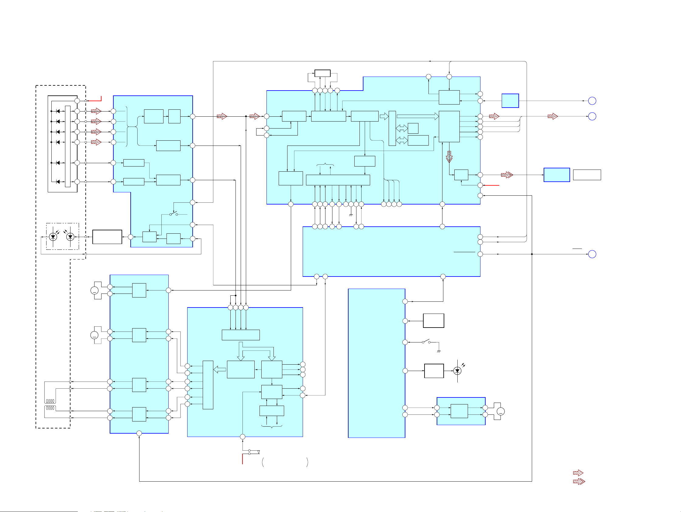
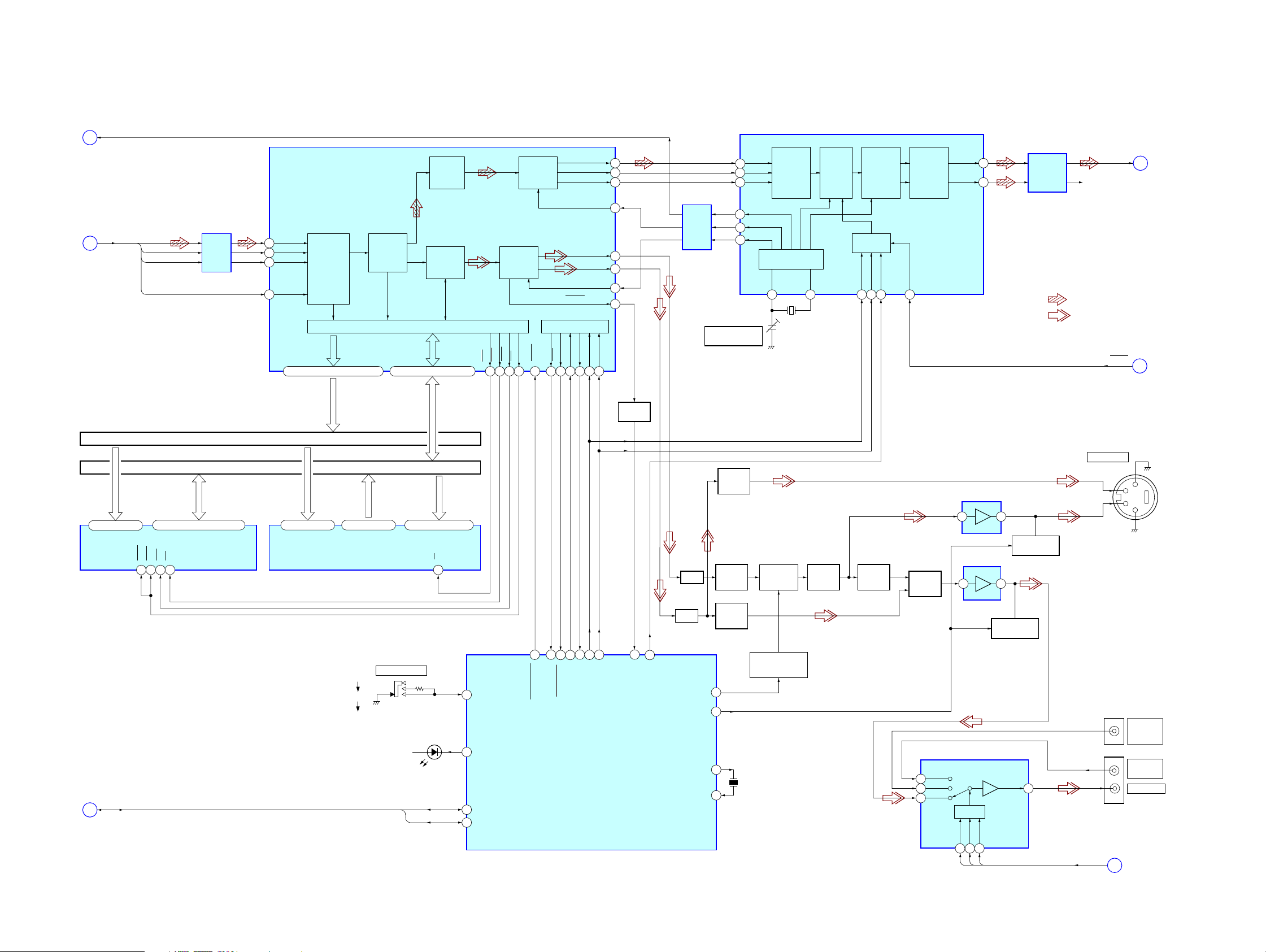
7-1. BLOCK DIAGRAM – CD SERVO Section –
DETECTOR
A
B
C
D
F
E
OPTICAL PICK-UP
BLOCK
(KSS-213DH)
LASER DIODE
PD
I-V AMP
10
LD
(SPINDLE)
7
4
2
1
5
6
M101
(SLED)
M102
CD D+5V
10
11
AUTOMATIC
POWER CONTROL
Q101
15
M
16
17
M
18
FOCUS/TRACKING ERROR AMP
A
5
B
6
C
7
D
8
F
F I-V AMP
E
E I-V AMP
LD
3
FOCUS/TRACKING COIL DRIVE,
SPINDLE/SLED MOTOR DRIVE
IC102
CH4OUTF
CH4OUTR
CH3OUTF
CH3OUTR
MOTOR
DRIVE
MOTOR
DRIVE
SECTION 7
DIAGRAMS
RF AMP,
IC103
RF
CH4SIN
CH3FIN
CH3RIN
RF EQ
AMP
FOCUS
ERROR AMP
TRACKING
ERROR AMP
APC PD
AMP
25
24
23
HOLD SW
SUMMING
AMP
APC LD
AMP
RFO
LDON
PD
16
FE
14
TE
13
21
22
4
DIGITAL SERVO
CTL2
PROCESSOR
IC101 (2/2)
40 41 39 43
FE
TE
SE
A/D
CONVERTER
DIGITAL SIGNAL PROCESSOR
50
49
48
RFDC
FILTER
IC101 (1/2)
RFAC
ASYMMETRY
CORRECTOR
ASYI
ASYO
DIGITAL
CLV
PROCESSOR
MDP
25 76 77
53 55
PCO
FILO
DIGITAL PLL
TO SERVO AUTO
SEQUENCER
DATA
CLOK
3 5 4 1 18 36 37 10
DSP CLK
DSP DATA
LDON
28 2
125254
FILI
CLTV
XPCK
CPU INTERFACE
SCOR
SENSE
XLAT
SENSE
DSP LATCH
SENSE CLK
16 69
C4M
EFM
DEMODULATOR
32K
RAM
INTERNAL BUS
SUBCODE
PROCESSOR
SQCK
SQSO
EXCK
SBSO
79 801574 6 5 10 111368 3
SCOR
SUBQ CLK
SUBQ DATA
WFCK
XUGF
GFS
CD MECHANISM CONTROLLER
IC502 (1/2)
XRST
T-SENS
ENC3/UP-SW
EMPH
CORRECTOR
59
61
68
ERROR
DISC TABLE
SENSOR
IC202
S201
(UP)
CTL2
CTL1
XTSL
CLOCK
GENERATOR
D/A
DIGITAL
INTERFACE
MUTE
DSP MUTE
XRESET
12
XTAO
XTAI
PCMD
BCK
LRCK
C2PO
WDCK
DOUT
DIGITAL
OUT
MD2
XRST
CTRL1
CTRL2
DEVICE RESET
72
71
66
67
65
14
17
64
63
2
11
27
77
OSC
BUFFER
IC104
DATA
BCK
LRCK
C2PO
CD D+5V
CTL1
CTL2
OPTICAL
TRANSCEIVER
IC781
MCLK
33.8MHz
DATA, BCK,
LRCK, C2PO
CD DIGITAL OUT
RESET
OPTICAL
A
B
C
(Page 19)
(Page 19)
(Page 19)
2-AXIS
DEVICE
(TRACKING)
(FOCUS)
12
11
14
13
CH2OUTF
CH2OUTR
CH1OUTF
CH1OUTR
COIL
DRIVE
COIL
DRIVE
MUTE
20
CH2FIN
CH2RIN
CH1FIN
CH1RIN
SFDR
29
SRDR
30
5
6
2
3
TFDR
31
TRDR
32
FFDR
33
FRDR
34
PWM GENERATOR
FOCUS/TRACKING/SLED
FOCUS/
TRACKING/SLED
SERVO DSP
SSTP
26
CD D+5V
MIRR,
DFCT, FOK
DETECTOR
SERVO
INTERFACE
SERVO AUTO
SEQUENCER
TO CPU INTERFACE
S101
(LIMIT)
ON: When the optical pick-up
is inner position.
FOK
MIRR
DFCT
COUT
SCLK
22
20
21
19
8
SYSTEM CONTROLLER
ENC2/DISC-LED
IC501 (1/4)
TBL-L
TBL-R
69
63
65
LED DRIVE
Q201
9
1
TABLE MOTOR DRIVER
IN1
IN2
IC201
MOTOR
DRIVE
D201
(DISC No.)
OUT1
OUT2
7
3
M201
M
(TABLE)
• SIGNAL PATH
: CD PLAY (ANALOG OUT)
: CD PLAY (DIGITAL OUT)
1818
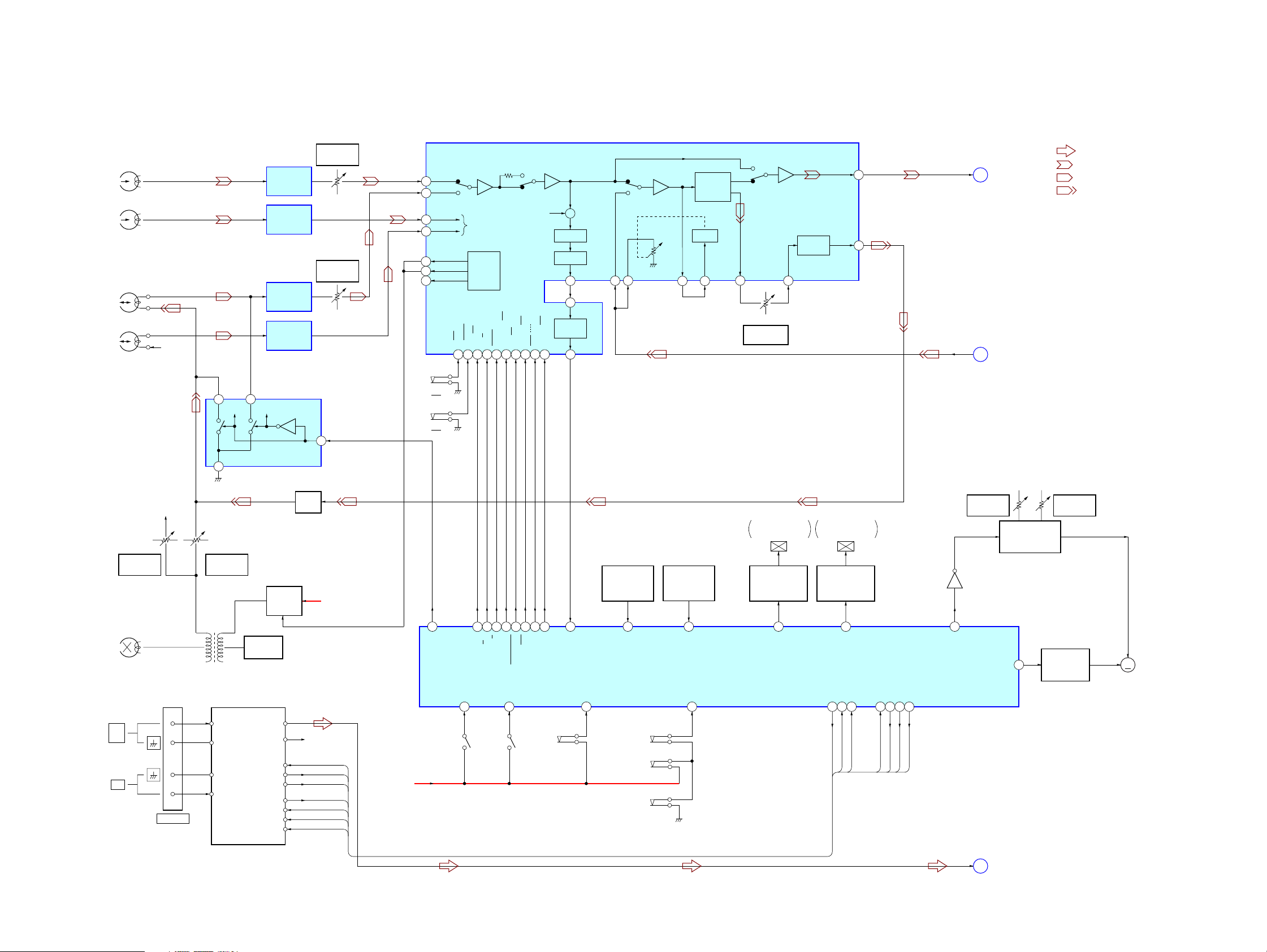
7-2. BLOCK DIAGRAM – AUDIO/VIDEO CD Section –
MCLK 33.8MHz
A
(Page 18)
B
(Page 18)
DATA, BCK,
LRCK, C2PO
DATA
BCK
LRCK
C2PO
LEVEL
SHIFT
IC501
MPEG VIDEO/AUDIO DECODER,
VIDEO SIGNAL PROCESSOR
IC505
CD-DATA
4
CD-BCK
3
5
6
CD-LRCK
CD-C2PO
CD-ROM
INTERFACE
CIRCUIT
MA0 – MA10
58 – 56, 54, 52 – 50, 48, 46 – 44 10 – 15, 17, 19, 21, 23 – 29
MPEG
SYSTEM
DECODER
D-RAM/ROM INTERFACE
MD0 – MD15
MPEG
AUDIO
DECODER
MPEG
VIDEO
DECODER
PROCESS
CIRCUIT
RAS0
MWE
MCE
37
38 42 40 60
VIDEO
CAS
AUDIO
INTERFACE
CIRCUIT
PGIO2/VSYNC/CSYNC
HRDY
RESET
113
DA-DATA
DA-BCK
DA-LRCK
DA-XCLK
Y-OUT
C-OUT
VCK-IN
CPU INTERFACE
HSEL
HD-OUT
HD-IN
HINT
114 121
112
119
117
HCK
HCD-GV6/GV8
DIGITAL FILTER,
D/A CONVERTER
IC509
XT1
DIGITAL
FILTER,
NOISE
SHAPER
CIRCUIT
D/A
CONVERTER
MODE
CONTROL
MC
MD
9 724 1
8
R-CH
CD-L
E
(Page 21)
LOW-PASS
FILER
VOUTL
VOUTR
14
11
LOW-PASS
FILER
IC101
• R-ch is omitted due to same as L-ch.
ML
RSTB
10
• SIGNAL PATH
: CD PLAY (AUDIO)
: CD PLAY (VIDEO)
RESET
C
(Page 18)
CT503
(27MHz)
DATA
18
BCK
17
LRCK
19
768FSO
21
384FSO
20
MCKO
4
INPUT
INTERFACE
CIRCUIT
TIMING CONTROL/
CLOCK GENERATOR
XT2
X503
27MHz
110
111
108
86
69
75
106
93
OSC
BUFFER
IC504
VIDEO FREQUENCY
16 – 19, 22 – 26
D-RAM
IC507
D
(Page 22)
A0 – A8
A0 – A8
DATA, CLK
UCAS
LCAS
14 132928
RAS
DQ1 – DQ16
WE
D0 – D15
ADDRESS BUS
DATA BUS
12 – 5, 27, 26, 23
PROGRAM ROM
A0 – A10
IC506
A0 – A10
A0 – A10
13 – 15, 17 – 212 – 5, 7 – 10, 31 – 34, 36 – 39
NTSC
AUTO
D0 – D7
O0 – O7
PAL
25, 4, 28, 29, 3, 2, 30
S501
SYSTEM SELECT
(SELF DIAGNOSIS)
D0 – D15
D8 – D14
A11 – A17
CE
22
D502
CLK
DATA
93
73
29
30
NT/PAL
TEST LED
CLK
DATA
24
2120
DATA1I
DATA1O
CL680 SEL
CL680 HINT
CL680 HRDY
CL680 RESET
CD MECHANISM CONTROLLER
IC502 (2/2)
32
23
BUFFER
Q502
DATA
CLK
VIDEO
BUFFER
Q303
XOUT
XIN
34
65
13
15
VIDEO
BUFFER
Q301
VIDEO
BUFFER
Q304
B.P.F.
B.P.F.
CLK1
45
22
BUS
DF LATCH
SHARPNESS
VMUTE
3331
SHARPNESS
FILTER
Q302
SHARPNESS
CONTROL SWITCH
Q306
X501
10MHz
VIDEO
BUFFER
Q307
VIDEO
BUFFER
Q308
VIDEO SELECT
SWITCH,
VIDEO AMP
IC191
Y/C MIX
Q310
IN1
1
IN3 VOUT
IN4
8
VIDEO AMP
IC401 (1/2)
VIDEO AMP
IC401 (2/2)
LOGIC
CTLA
CTLB
3 52
ABC
VIDEO MUTING
CTLC
41
VIDEO MUTING
58
Q454
Q453
106
J301
S VIDEO OUT
C
Y
J804 (1/2)
J702
A, B, C
F
1
3
4
2
GAME
INPUT
VIDEO
VIDEO
VIDEO IN
VIDEO OUT
(Page 21)
1919
HCD-GV6/GV8
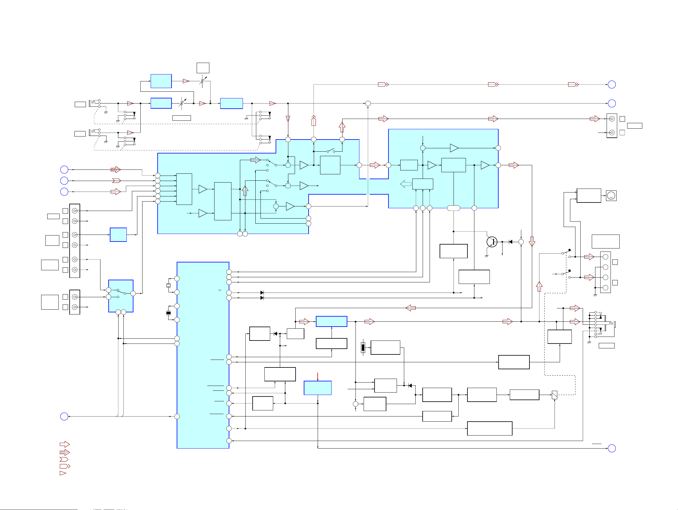
7-3. BLOCK DIAGRAM – TUNER/TAPE DECK Section –
HP101
(PLAYBACK)
L-CH
R-CH
HRPE101 (1/2)
(RECORD/PLAYBACK)
L-CH
R-CH
R-CH
DECK PROCESS,
DECK A/B SELECT, PB/REC EQ AMP,
DOLBY NR AMP, ALC, AMS
RV311
PB LEVEL (L)
(DECK A)
PB EQ AMP
(DECK A)
IC611 (2/2)
PB EQ AMP
(DECK A)
IC611 (1/2)
RV301
PB LEVEL (L)
(DECK B)
PB EQ AMP
(DECK B)
IC601 (2/2)
PB EQ AMP
(DECK B)
IC601 (1/2)
REC/PB SWITCHING
IC602
1
3
R-CH
R-CH
4
A IN (L)
48
B IN (L)
46
A IN (R)
51
B IN (R)
53
BIAS (N)
33
BIAS (C)
32
BIAS (M)
31
S1004
(DECK A 120/70)
S1008
(DECK B 120/70)
IC301
R-CH
BIAS
CONTROL
CIRCUIT
B NORM/CROM
ALC ON/OFF
A 120/70
1516182022 23242517
19
NORM/HIGH
PB A/B
70
120
R-CH
NR ON/OFF
BIAS ON/OFF
RM ON/OFF
L.P.F.
BUFFER
AMS
CIRCUIT
REC/PB/PASS
LM ON/OFF
+
28
27
26
MAOUT
MSIN
MSOUT
R IN (L)
43
ALC (L)
44
DOLBY PASS
ALC
R OUT (L)
35 34
DOLBY NR
AMP
CIRCUIT
ALC
IN (L)
REC OUT (L)
39
RV301
REC LEVEL (L)
(DECK B)
EQ IN (L)
38
REC
EQ AMP
PB OUT (L)
EQ OUT
40
(L)
36
PB-L
REC-L
G
(Page 21)
H
(Page 21)
• R-ch is omitted due to same as L-ch.
• SIGNAL PATH
: TUNER (FM/AM)
: PLAYBACK (DECK A)
: PLAYBACK (DECK B)
: RECORD
RV441
REC BIAS (R)
(DECK B)
HRPE101 (2/2)
(ERASE)
FM
75Ω
AM
R-CH
ANTENNA
2
RV341
REC BIAS (L)
(DECK B)
BIAS OSC
T621
FM/AM TUNER UNIT
FM ANT
FM ANT
AM ANT
AM ANT
BIAS OSC
Q621, 622
ST-R
ST-MUTE
STEREO
TUNED
ST-DIN
ST-DOUT
ST-CLK
ST-CE
REC BIAS
SWITCH
Q623
ST-L
C331, L331
BIAS
TRAP
R-CH
ST-MUTE
STEREO
TUNED
ST-DIN
ST-DOUT
ST-CLK
ST-CE
A+7V
D+5V
(UNSW)
100
TC-RELAY
(DECK A PLAY)
8584838281 807978
ALC
PB-A/B
EQ-H/N
A-PLAY-SW
87
S1001
S1002
(DECK B PLAY)
BIAS
REC-MUTE
B-PLAY-SW
86
TC-MUTE
R/PB/PAS
NR-ON/OFF
(DECK A HALF)
S1003
77
AMS-IN
A-HALF
88
ROTATION
DETECT SENSOR
(DECK A)
IC1001
91
A-SHUT
S1006
(DECK B HALF)
S1005
(DECK A REC)
S1009
(DECK B REC)
ROTATION
DETECT SENSOR
(DECK B)
IC1002
90
B-SHUT
B-HALF
89
TRIGGER PLUNGER
PLUNGER DRIVE
SYSTEM CONTROLLER
IC501 (2/4)
DECK A
TRIGGER
(DECK A)
Q333, 334
73
A-TRG
TRIGGER PLUNGER
DECK B
TRIGGER
PLUNGER DRIVE
(DECK B)
Q331, 332
72
B-TRG
ST-DIN
TUNED
STEREO
ST-MUTE
49 50 51 54 53 55 52
ST-DIN
TUNED
STEREO
ST-MUTE
ST-CLK
ST-DOUT
ST-CLK
ST-DOUT
ST-CE
ST-CE
Q335
76
CAP-M-H/L
RV1001
TAPE SPEED
(HIGH)
CAPM-CNT2
CAPSTAN MOTOR
CONTROL SWITCH
Q1001
74
MOTOR DRIVE
RV1002
TAPE SPEED
(NORMAL)
CAPSTAN
Q336, 339
M
M1
(CAPSTAN)
CT-L
J
(Page 21)
2020
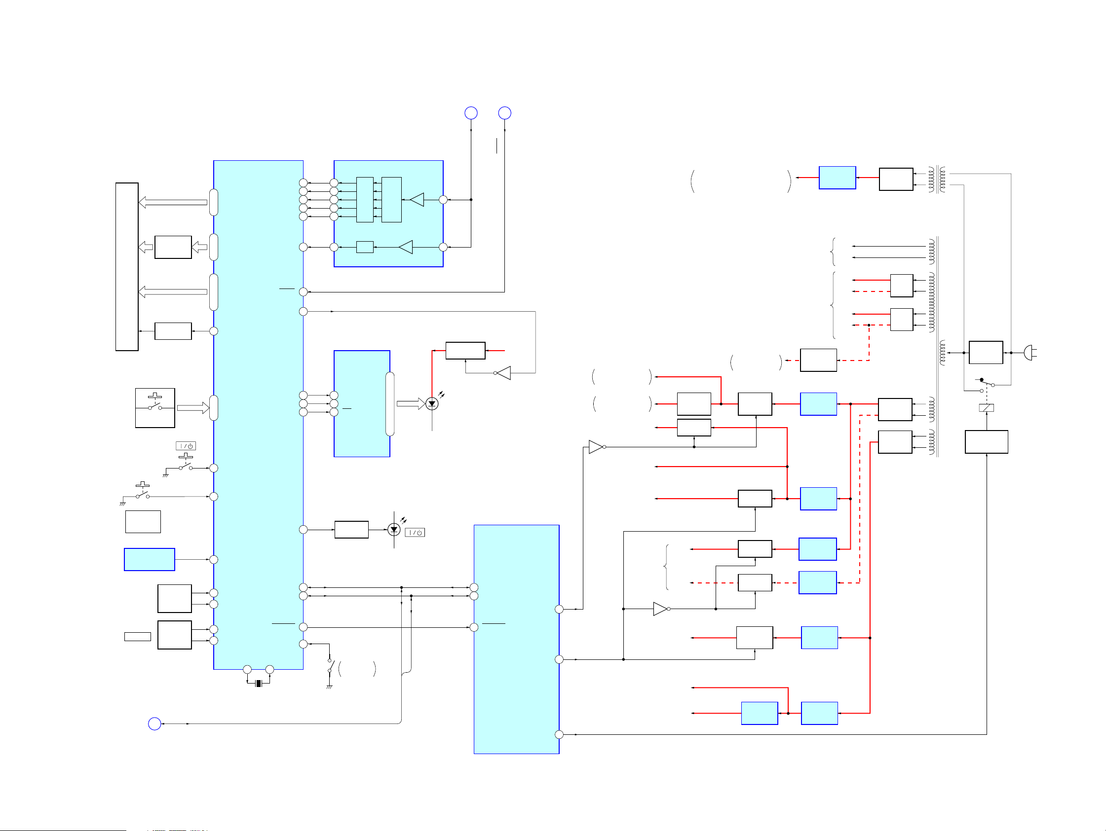
7-4. BLOCK DIAGRAM – MAIN Section –
DIGITAL
ECHO
IC851
RV601
ECHO
LEVEL
HCD-GV6/GV8
REC-L
H
(Page 20)
J802
MIC 2
J801
MIC 1
E
G
J
J701 (1/2)
L
R
L
R
L
R
J804 (2/2)
L
R
F
CD-L
PB-L
ST-L
R-CH
R-CH
R-CH
R-CH
A, B, C
(Page 19)
(Page 20)
(Page 20)
MD IN
PHONO
IN
VIDEO
AUDIO IN
GAME
INPUT
AUDIO
(Page 19)
• R-ch is omitted due to same as L-ch.
• SIGNAL PATH
: TUNER (FM/AM)
: CD PLAY
: TAPE PLAY
: RECORD
: MIC INPUT
PHONO
EQ AMP
IC601
FUNCTION SELECT
SWITCH
IC181
X0
12
14
X1
X
AB
10 9
MIC AMP
IC850 (1/2)
RV602
MIC LEVEL
INPUT SELECT SWITCH,
GRAPHIC EQUALIZER CONTROL,
ELECTRICAL VOLUME
IN D2
66
IN C2
67
IN B2
68
IN E2
65
IN A2
69
IN F2
64
IC101
INPUT
SELECT
SWITCH
R-CH
MIC AMP
IC850 (2/2)
SOUND
CONTROL
CIRCUIT
KEY IN2
KEY IN1
60 5
2 58 57
MIC IN
REC A2
+
+
L+R
+
KEY OUT 1
KEY OUT 2
30
6
59
GRAPHIC
EQUALIZER
CONTROL
CIRCUIT
R-CH
REC B2
F OUT2
42 41
+
R-CH
SUPER
WOOFER
72
BUF
OUT2
36
FEED BACK
SWITCH
Q112
R-CH
D803
VOL
IN2
COMMAND
VOLUME
CONTROL
+
CPU
INTERFACE
DATA
CLOCK
LATCH
34
BASS BOOST
CONTROL
CIRCUIT
BB B2,
BB A2
38, 39
BUF IN2
373233
+
DBFB CONTROL
SWITCH
Q111
493-DATA
XC-OUT
X501
13
32.768kHz
X502
16MHz
11
XC-IN
10
13
X-OUT
X-IN
15
FUNC SEL0
46
FUNC SEL1
45
CBA
28
V MUTE
SW-MODE
SYSTEM CONTROLLER
IC501 (3/4)
STK-POWER
LINE-MUTE
493-CLK
493-LAT
DBFB-H/L
HP MUTE
AC-CUT
RESET
PROTECT
F-RELAY
HP-IN
47
48
38
7
34
1
93
6
22
12
27
3
36
D501
D534
PROTECT
SWITCH
Q804
RESET
SWITCH
Q801
D807
R-CH
MUTING CONTROL
SWITCH
Q802, 803
MUTING
Q113
POWER AMP
STANDBY SWITCH
Q803, 804, 834
EVER +5V
RESET SIGNAL
GENERATOR
IC801
IC801
R-CH
+
R-CH
TH831
TEMPERATURE
DETECT SWITCH
OVER LOAD
DC DETECT
SWITCH
Q433, 434
Q831, 832
DETECT
Q801, 851
D401
OVER LOAD
DETECT SWITCH
Q432
PROTECT SWITCH
Q439
BASS WOOFER
CONTROL SWITCH
Q115
R-CH
OVER LOAD
DETECT SWITCH
Q437
FRONT SPEAKER PROTECT
RELAY DRIVE
R-CH
Q401, 402
R-CH
MUTING CONTROL
SWITCH
Q833
PROTECT SWITCH
Q431
R-CH
R-CH
–1
–2
HEADPHONE
MUTING
Q805, 855
RY401
SPEANA
R-CH
FAN MOTOR
DRIVE
Q961, 962
FRONT SPEAKER
RESET
K
J701 (2/2)
M901
(FAN)
M
TM401
IMPEDANCE
USE 4 – 16Ω
+
–
+
–
J803
PHONES
L
(Page 22)
L
MD OUT
R
L
R
(Page 22)
2121
HCD-GV6/GV8
7-5. BLOCK DIAGRAM – DISPLAY/KEY CONTROL/POWER SUPPLY Section –
K
(Page 21)(Page 21)
L
GRID DRIVE
Q605, 606
FL601
FLUORESCENT INDICATOR TUBE
GRID DRIVE
Q607
S601 – 607, 611 – 619, 621 – 627,
S701 – 730, 735, 741, 743 – 762
S608
S609
POWER
SAVE/DEMO
(STANDBY)
REMOTE CONTROL
RECEIVER
IC702
D
(Page 19)
ROTARY
ENCODER
S763
ROTARY
ENCODER
S736
DATA, CLK
S763
(JOG DIAL)
S736
VOLUME
FLUORESCENT INDICATOR TUBE DRIVER,
43
74
75
10
KEY CONTROL
44 – 46
SEG-1 – SEG-23
28 , 27
GR-15, GR-16
42, 40 – 29
GR-2 – GR-14
GR-1
11 – 15
KEY 0 – KEY 4
4
KEY POWER ON/OFF
KEY POWER
2
SAVE/DEMO
1
SIRCS
JOG A
JOG B
VOL A
9
VOL B
72 70
IC601
LED STANDBY
XOUT
X601
12.5MHz
BPF 0
BPF 1
BPF 2
BPF 3
BPF 4
ALL BAND
RESET
LED SEL
LED DAT
LED SCK
LED LATCH
I2C DATA
I2C CLK
WAKE UP
D-SW
XIN
17
18
19
20
21
22
73
67
78
79
80
RECT
D832
RECT
D831
SUB POWER
TRANSFORMER
T901
POWER
TRANSFORMER
T951
VOLTAGE
SELECTOR
S901
RY901
POWER ON/OFF
RELAY DRIVE
Q901
AC IN
BAND-PASS FILTER
IC602
F02
16
F03
15
F04
14
13
12
11
7
5
13
3
14
6
15
8
F05
F06
REC
LEVEL
LED DRIVER
IC701
DATA
CLK
STB
LED DRIVE
Q601
S742
LID (CD)
OPEN/CLOSE
DET
DET
P1 – P6, P7 – P10, P12 – P16
B.P.F.
17, 19 – 23, 1 – 4, 7 – 11
DATA
D601
CLK
LINE
REC IN
IN
SPEANA
4
6
B+ SWITCH
Q602, 603
D611 – 614, 621, 622,
D700 – 710, 713, 714,
D716 – 720, 741, 791
30
29
18
RESET
+5V (LED)
Q604
SYSTEM CONTROLLER
IC501 (4/4)
IIC-DATA
IIC-CLK
CD-POWER
WAKE UP
STBY RELAY
POWER
EVER +5V
SYSTEM CONTROLLER (IC501),
CD MECHANISM CONTROLLER (IC502),
FL DRIVER (IC601) B+
TO FLUORESCENT
INDICATOR TUBE
(FL601)
POWER AMP (IC801),
PROTECT CIRCUIT
–35V
CD D+5V (SW)
CD STEREO/VIDEO CD
SECTION B+
+3.3V
MPEG VIDEO/AUDIO
DECODER (IC505) B+
CD A+5V (SW)
(VIDEO CD SECTION B+)
Q914
+5V (LED)
(PANEL SECTION B+)
D+5V (UNSW)
AU D+5V
M62493FP (IC101) B+
D+5V (SW)
(CD SENSOR SECTION B+)
TC, PANEL,
AUDIO
5
Q906
ST +10V
(FM/AM TUNER UNIT B+)
2
FAN MOTOR B+
TC M+12V
(TC MOTOR SECTION B+)
CD M+7V
(CD MOTOR SECTION B+)
43
+3.3V
REGULATOR
Q531
B+ SWITCH
Q913
A+7V
A–7V
FL DRIVER (IC601)
B–
VCD
B+ SWITCH
Q921
B+ SWITCH
Q911, 912
B+ SWITCH
Q901, 902
B– SWITCH
Q903 – 905
TUNER
B+ SWITCH
Q931, 932
+7V
REGULATOR
IC933
REGULATOR
REGULATOR
REGULATOR
REGULATOR
REGULATOR
REGULATOR
–35V
Q903, 908
+5V
IC921
+5V
IC911
+7V
IC901
–7V
IC951
+10V
REGULATOR
IC931
+12V
REGULATOR
IC932
+5V
IC901
+VL
–VL
+VH
–VH
RECT
D902 – 905
VF
VF
RECT
D841 – 844
RECT
D833 – 836
2222
HCD-GV6/GV8
CD-R (1) board
TC-B board
CD-L board
TC-A board
MIC board
ILLUMINATION board
PANEL VR board
PANEL FL board
TRANS board SUB TRANS board
TUNER PACK
(FM/AM TUNER UNIT)
MAIN board
PA board
HEADPHONES board
CD-R (2) board
FRONT INPUT board
VIDEO board
7-6. NOTE FOR PRINTED WIRING BOARDS AND SCHEMATIC DIAGRAMS
Note on Printed Wiring Board:
• X : parts extracted from the component side.
• Y : parts extracted from the conductor side.
• : Pattern from the side which enables seeing.
(The other layers' patterns are not indicated.)
Caution:
Pattern face side: Parts on the pattern face side seen from
(Side B) the pattern face are indicated.
Parts face side: Parts on the parts face side seen from
(Side A) the parts face are indicated.
• Indication of transistor.
C
Q
B
B
B
E
Q
CE
These are omitted.
These are omitted.
Q
CE
These are omitted.
Note on Schematic Diagram:
• All capacitors are in µF unless otherwise noted. pF: µµF
50 WV or less are not indicated except for electrolytics
and tantalums.
• All resistors are in Ω and 1/
specified.
• 2 : nonflammable resistor.
• 5 : fusible resistor.
• C : panel designation.
Note: The components identified by mark 0 or dotted line
with mark 0 are critical for safety.
Replace only with part number specified.
• A : B+ Line.
• B : B– Line.
• H : adjustment for repair.
• V oltages are taken with a VOM (Input impedance 10 MΩ).
Voltage variations may be noted due to normal production tolerances.
• Waveforms are taken with a oscilloscope.
Voltage variations may be noted due to normal production tolerances.
• Circled numbers refer to waveforms.
• Signal path.
F : TUNER (FM/AM)
E : TAPE PLAY (DECK A)
d : TAPE PLAY (DECK B)
G : RECORD
L : CD PLAY (VIDEO)
J : CD PLAY (AUDIO)
c : DIGITAL OUT
N : MIC INPUT
• Abbreviation
EA : Saudi Arabia model
IA : Indonesia model
MY : Malaysia model
SP : Singapore model
4
• Circuit Boards Location
W or less unless otherwise
TABLE SENSOR board
CD MOTOR board
LEAF SW board
BD board
AUDIO board
LED board
2323
HCD-GV6/GV8
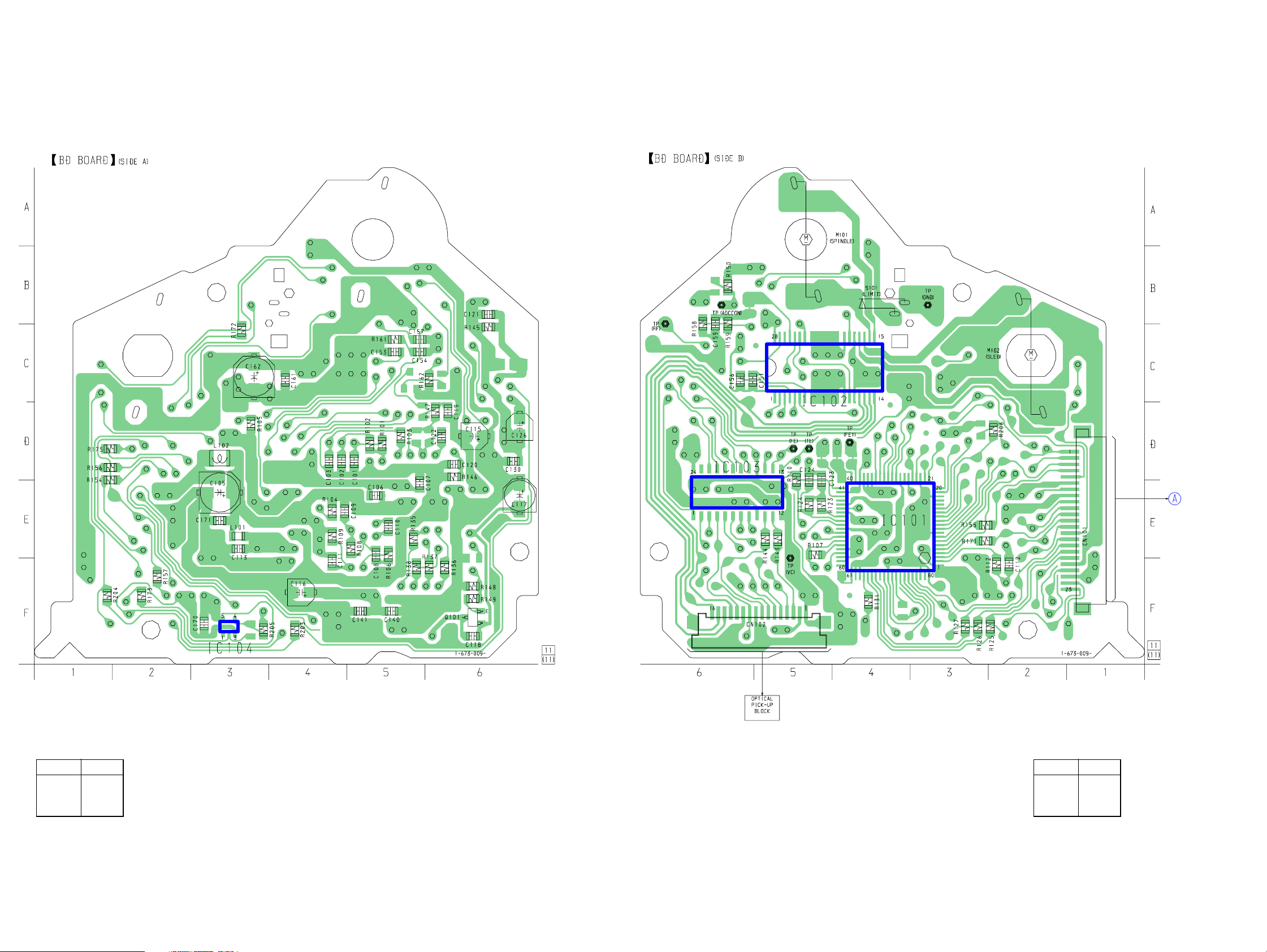
7-7. PRINTED WIRING BOARD – BD Board –• See page 23 for Circuit Boards Location.
• Semiconductor
Location
(Side A)
Ref. No. Location
IC104 F-3
Q101 F-6
(KSS-213DH)
• Semiconductor
Location
(Side B)
Ref. No. Location
IC101 E-4
IC102 C-5
IC103 E-6
VIDEO
BOARD
CN501
(Page
28)
2424
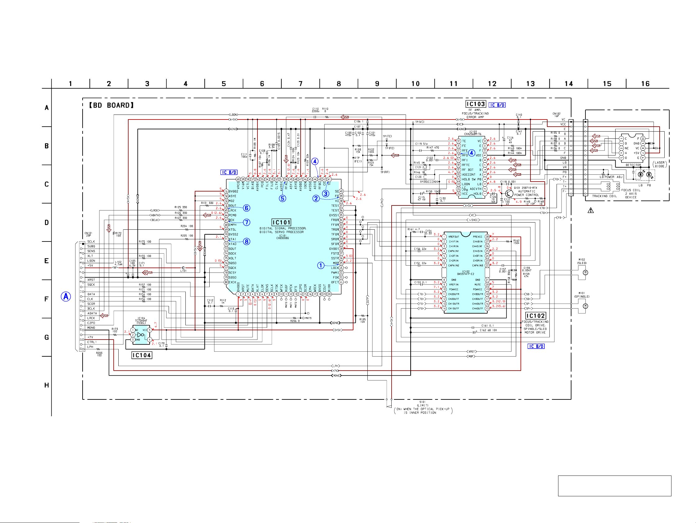
7-8. SCHEMATIC DIAGRAM – BD Board –• See page 39 for Waveforms. • See page 51 for IC Block Diagrams.
HCD-GV6/GV8
VIDEO
BOARD
(1/2)
CN501
(Page 26)
D. OUT
D. GND
AMUTE
XTAL33.8MHz
OPTICAL PICK-UP
BLOCK
(KSS-213DH)
OSC BUFFER
• Voltages and waveforms are dc with respect to ground
under no-signal conditions.
no mark : CD STOP
( ) : CD PLAY
The components identified by mark 0 or dotted
line with mark 0 are critical for safety.
Replace only with part number specified.
2525
HCD-GV6/GV8
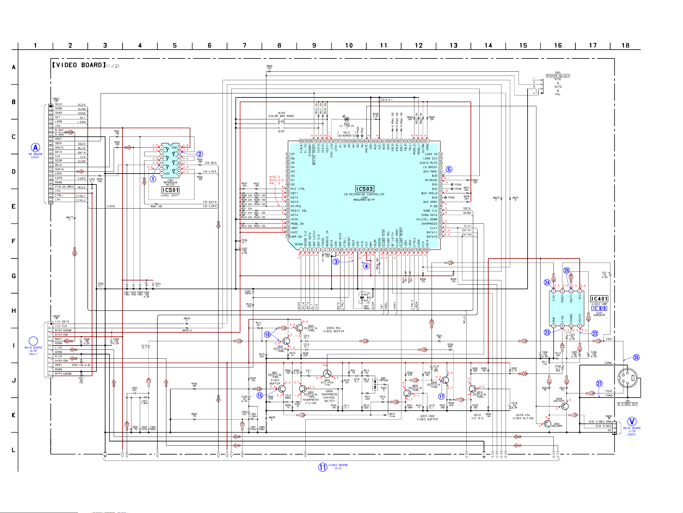
7-9. SCHEMATIC DIAGRAM – VIDEO Board (1/2) –• See page 29 for Waveforms. • See page 51 for IC Block Diagrams.
(Page 25)
W
(Page 36)
2626
(Page 27)
(Page 35)
• Voltages and waveforms are dc with respect to ground
under no-signal conditions.
no mark : VIDEO CD PLAY
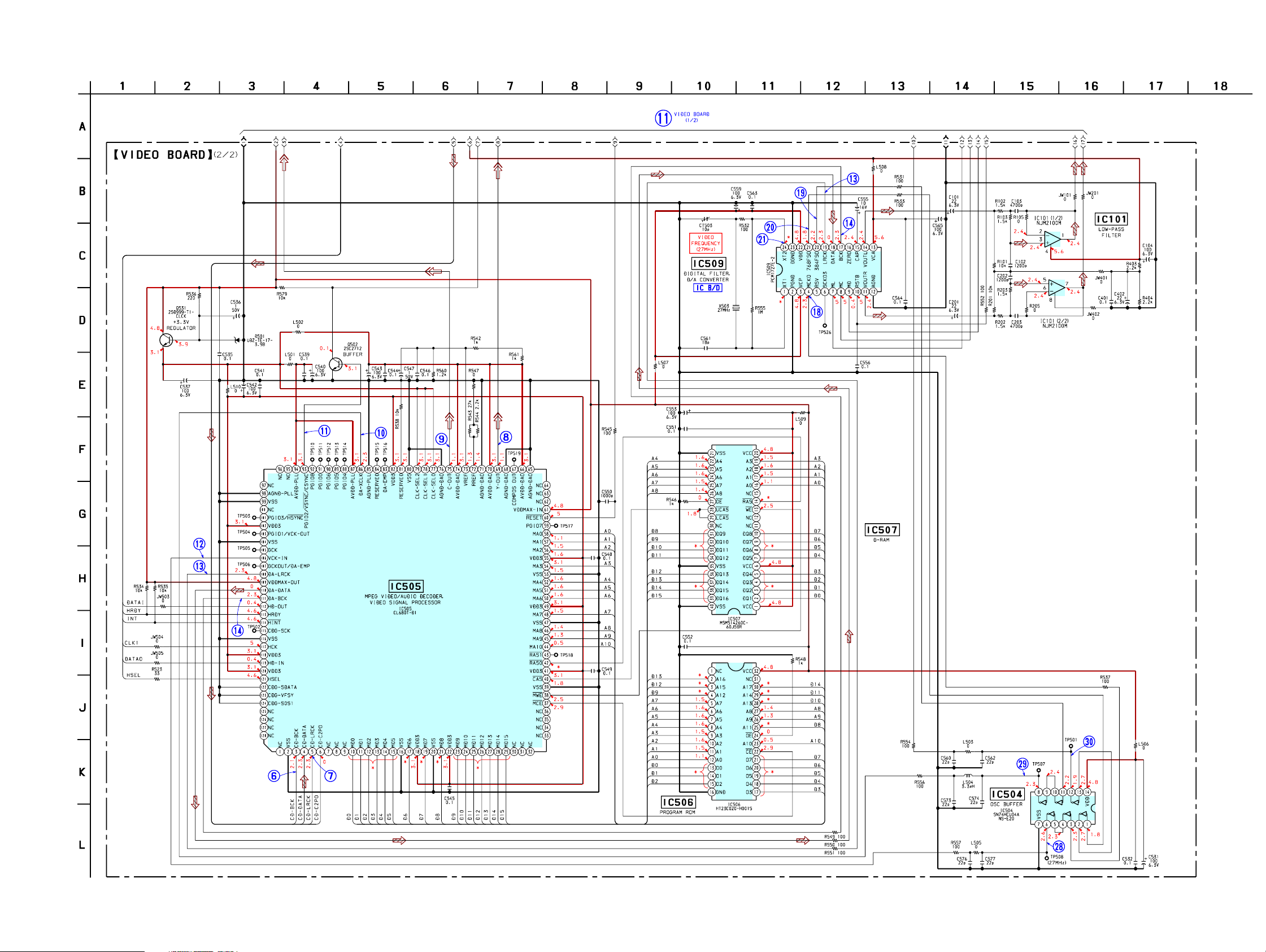
7-10. SCHEMATIC DIAGRAM – VIDEO Board (2/2) –• See page 29 for Waveforms. • See page 51 for IC Block Diagrams.
HCD-GV6/GV8
(Page 26)
• Voltages and waveforms are dc with respect to ground
under no-signal conditions.
no mark :VIDEO CD PLAY
2727
: Impossible to measure
∗
HCD-GV6/GV8
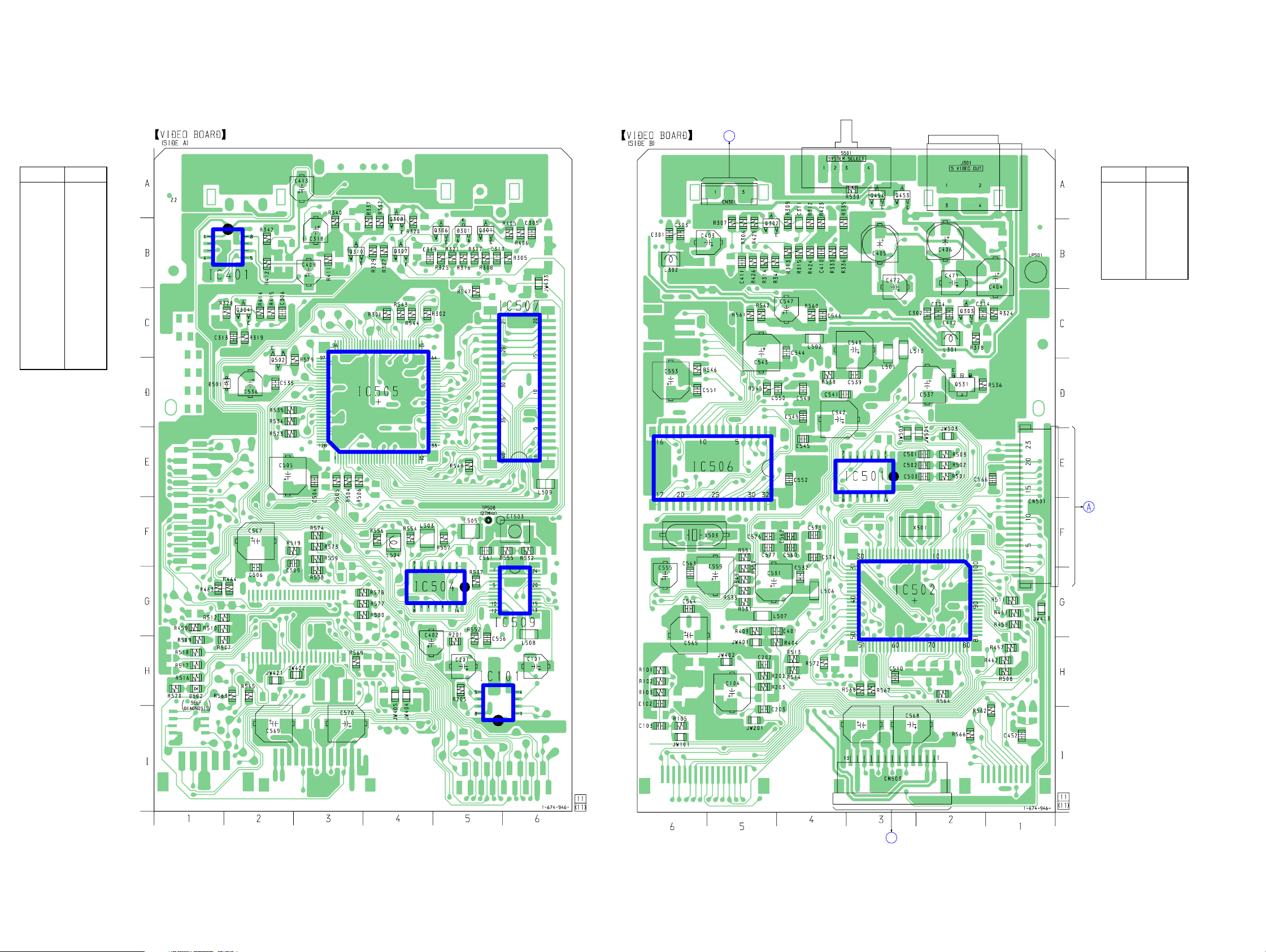
7-11. PRINTED WIRING BOARD – VIDEO Board –• See page 23 for Circuit Boards Location.
• Semiconductor
Location
(Side A)
Ref. No. Location
D301 B-5
D501 D-2
D502 H-1
(Page 38)
MAIN BOARD
V
CN701
• Semiconductor
Location
(Side B)
Ref. No. Location
IC501 E-3
IC502 G-3
IC506 E-5
IC101 H-5
IC401 B-2
IC504 G-5
IC505 D-4
IC507 D-6
IC509 G-6
Q301 B-5
Q304 C-2
Q306 B-5
Q307 B-4
Q308 B-4
Q310 B-3
Q502 D-2
BD
BOARD
CN101
(Page 24)
Q302 B-5
Q303 C-2
Q453 A-3
Q454 A-3
Q531 D-2
C571
MAIN BOARD
W
CN411
(Page 38)
2828
 Loading...