

Sony HCDGRX-9900 Service manual
HCD-GRX9900/RXD9
SERVICE MANUAL
HCD-GRX9900/RDX9 are the Amplifier,
CD player, Tape Deck and Tuner section
in MHC-GRX9900/RXD9.
Dolby noise reduction manufactured under license
from Dolby Laboratories Licensing Corporation.
“DOLBY” and the double-D symbol a are trademarks of Dolby Laboratories Licensing Corporation.
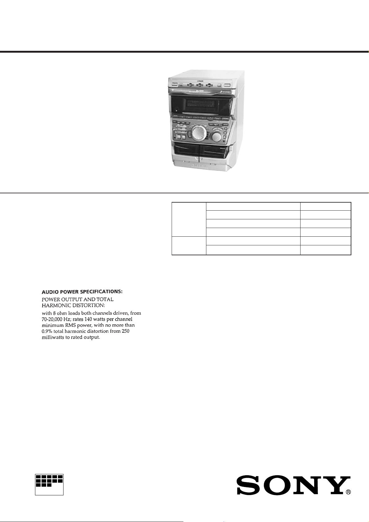
Photo: HCD-RXD9 (US model)
CD
Section
Tape deck
Section
US Model
AEP Model
UK Model
HCD-RXD9
E Model
HCD-GRX9900
Model Name Using Similar Mechanism NEW
CD Mechanism Type CDM38LH-5BD32L
Base Unit Name BU-5BD32L
Optical Pick-up Name KSS-213D/Q-NP
Model Name Using Similar Mechanism NEW
Tape Transport Mechanism Type TCM-230AWR2
Amplifier section
US model:
AEP and UK models:
DIN power output (rated) 120 + 120 watts
(8 ohms at 1 kHz, DIN)
Continuous RMS power output (reference)
150 + 150 watts
(8 ohms at 1 kHz, 10% THD)
Music power output (reference)
275 + 275 watts
(8 ohms at 1 kHz, 10% THD)
SPECIFICATIONS
E models:
The following measured at AC 120, 220, 240 V 50/60 Hz
DIN power output (rated) 200 + 200 watts
(6 ohms at 1 kHz, DIN)
Continuous RMS power output (reference)
250 + 250 watts
(6 ohms at 1 kHz, 10% THD)
– Continued on next page –
MICROFILM
MINI Hi-Fi COMPONENT SYSTEM

Specifications (continued)
Inputs
MD/VIDEO (AUDIO) IN: voltage 450 mV/250mV,
(phono jacks) impedance 47 kilohms
MIX MIC: (phone jack) sensitivity 1 mV, impedance 10
kilohms
Outputs
MD OUT: voltage 250 mV,
(phono jacks) impedance 1 kilohms
PHONES: accepts headphones of 8 ohms
(stereo phone jack) or more
SPEAKER:
E models: accepts impedance of 6 to 16 ohms
Other models: accepts impedance of 8 to 16 ohms
SUPER WOOFER (GRX9900/RXD9: US models):
Voltage 1 V, impedance 1 kilohm
CD player section
System Compact disc and digital audio system
Laser Semiconductor laser (λ=780nm)
Emission duration: continuous
Laser output Max. 44.6 µW*
*This output is the value measured at
distance of 200 mm from the objective
lens surface on the Optical Pick-up
Block with 7 mm aperture.
Frequency response 2 Hz - 20 kHz (±0.5 dB)
Wavelength 780 -790 nm
Signal-to-noise ratio More than 90 dB
Dynamic range More than 90 dB
CD OPTICAL DIGITAL OUT
(Square optical connector jack, rear panel)
Wavelength 600 nm
Output Level -18 dBm
Tape player section
Recording system 4-track 2-channel stereo
Frequency response 40 - 13,000 Hz (±3 dB),
(DOLBY NR OFF) using Sony TYPE I cassette
40 - 14,000 Hz (±3 dB),
using Sony TYPE II cassette
Tuner section
FM stereo, FM/AM superheterodyne tuner
FM tuner section
Tuning range 87.5 - 108.0 MHz
Antenna FM lead antenna
Antenna terminals 75 ohm unbalanced
Intermediate frequency 10.7 MHz
3 Band type:
Saudi Arabia model:
MW: 531 - 1,602 kHz
(with the interval set at 9 kHz)
SW: 5.95 - 17.90 MHz
(with the interval set at 5 kHz)
Other models:
MW: 531 - 1,602 kHz
(with the interval set at 9 kHz)
530 - 1,710 kHz
(with the interval set at 10 kHz)
SW: 5.95 - 17.90 MHz
(with the interval set at 5 kHz)
Antenna AM loop antenna
Antenna terminals External antenna terminal
Intermediate frequency 450 kHz
General
Power requirements
US model: 120 V AC, 60 Hz
AEP and UK models: 230 V A C, 50/60 Hz
Mexican model: 120 V AC, 50/60 Hz
Other models: 120 V, 220 V, or 230 - 240 V AC,
50/60 Hz
Adjustable with voltage selector
Power consumption
US model: 170 watts
AEP and UK models: 180 watts
Other models: 240 watts
Dimensions (w/h/d) Approx. 280 × 360 × 395 mm
(131/8 × 141/4 × 155/8 in.)
Mass
US model: Approx. 10.6 kg (23 lb 6 oz.)
AEP and UK models: Approx. 10.8 kg
Other models: Approx. 12.2 kg
Supplied accessories: AM loop antenna (1)
Remote Commander (1)
Batteries (2)
FM lead antenna (1)
Speaker cords (2)
Front speaker pads (8)
Design and specifications are subject to change without notice.
UKV tuner section (3 band (FM-AM-UKV) models only)
Tuning range 65.0 - 74.0 MHz
Stereo Plus
AM tuner section
Tuning range
2 Band type:
US model: 530 - 1,710 kHz
(with the interval set at 10 kHz)
531 - 1,710 kHz
(with the interval set at 9 kHz)
AEP and UK models:
531 - 1,602 kHz
(with the interval set at 9 kHz)
Other models: 531 - 1,602 kHz
(with the interval set at 9 kHz)
530 - 1,710 kHz
(with the interval set at 10 kHz)
SAFETY-RELATED COMPONENT WARNING!!
COMPONENTS IDENTIFIED BY MARK ! OR DOTTED
LINE WITH MARK ! ON THE SCHEMATIC DIA GRAMS
AND IN THE PARTS LIST ARE CRITICAL TO SAFE
OPERATION. REPLACE THESE COMPONENTS WITH
SONY PARTS WHOSE PART NUMBERS APPEAR AS
SHOWN IN THIS MANUAL OR IN SUPPLEMENTS PUBLISHED BY SONY.
– 2 –
TABLE OF CONTENTS
SECTION 1
SERVICING NOTES
1. SERVICING NOTES............................................... 3
2. GENERAL
Location of Controls ....................................................... 6
Setting the Time .............................................................. 7
3. DISASSEMBLY ......................................................... 8
4. TEST MODE.............................................................. 11
5. MECHANICAL ADJUSTMENTS....................... 14
6. ELECTRICAL ADJUSTMENTS
DECK Section ................................................................. 14
CD Section ...................................................................... 17
7. DIAGRAMS
7-1. Block Diagram – CD SERVO Section – ........................ 19
7-2. Block Diagram – TAPE DECK Section – ...................... 21
7-3. Block Diagram – MAIN Section –................................. 23
7-4. Block Diagram – DISPLAY/KEY CONTROL/
POWER SUPPLY Section – ........................................... 25
7-5. Note for Printed Wiring Boards and
Schematic Diagrams ....................................................... 27
7-6. Printed Wiring Board – BD Board – .............................. 29
7-7. Schematic Diagram – BD Board – ................................ 31
7-8. Printed Wiring Boards – CD MOTOR Section –.......... 33
7-9. Schematic Diagram – CD MOTOR Section – .............. 35
7-10. Pr inted Wiring Board – AUDIO Board – ...................... 37
7-11. Schematic Diagram – AUDIO Board – ......................... 39
7-12. Printed Wiring Board – LEAF SW Board –.................. 41
7-13. Schematic Diagram – LEAF SW Board – ..................... 41
7-14. Pr inted Wiring Board – MAIN Board – ........................ 43
7-15. Schematic Diagram – MAIN Board (1/4) – .................. 45
7-16. Schematic Diagram – MAIN Board (2/4) – .................. 47
7-17. Schematic Diagram – MAIN Board (3/4) – .................. 49
7-18. Schematic Diagram – MAIN Board (4/4) – .................. 51
7-19. Printed Wiring Board – PANEL/CD SW Board – ........ 53
7-20. Schematic Diagram
– PANEL (1/3)/CD SW Board –..................................... 55
7-21. Schematic Diagr am – PANEL (2/3) Board – ................ 57
7-22. Schematic Diagram – PANEL (3/3) Board – ................ 59
7-23. Pr inted Wiring Board – TRANS Board –....................... 61
7-24. Schema tic Diagr am – TRANS Board –......................... 62
7-25. Printed Wiring Board
– SUB TRANS Board (RXD9) –.................................... 63
7-26. Schematic Diagram
– SUB TRANS Board (RXD9) –.................................... 64
7-27. IC Pin Function Description ........................................... 69
SAFETY CHECK-OUT
After correcting the original service problem, perform the following safety check before releasing the set to the customer:
Check the antenna terminals, metal trim, “metallized” knobs,
screws, and all other exposed metal parts for AC leakage.
Check leakage as described below.
LEAKAGE TEST
The A C leaka ge from an y e xposed metal part to earth g round and
from all exposed metal parts to any exposed metal part having a
return to chassis, must not exceed 0.5 mA (500 microampers.).
Leakage current can be measured by any one of three methods.
1. A commercial leakage tester , such as the Simpson 229 or RCA
WT -540A. Follo w the manufacturers’ instructions to use these
instruments.
2. A battery-operated AC milliammeter. The Data Precision 245
digital multimeter is suitable for this job.
3. Measuring the voltage drop across a resistor by means of a
VOM or battery-operated AC voltmeter. The “limit” indication is 0.75 V, so analog meters must have an accurate lowvoltage scale. The Simpson 250 and Sanwa SH-63T rd are e xamples of a passive VOM that is suitable. Nearly all battery
operated digital multimeters that have a 2 V A C range are suitable. (See Fig. A)
To Exposed Metal
Parts on Set
AC
1.5 k
0.15 µF
Fig. A. Using an AC voltmeter to check AC leakage.
Ω
Earth Ground
voltmeter
(0.75 V)
8. EXPLODED VIEWS ................................................ 7 4
9. ELECTRICAL PARTS LIST ............................... 83
– 3 –
This appliance is classified as a CLASS 1 LASER product.
The CLASS 1 LASER PRODUCT MARKING is located on
the rear exterior.
Laser component in this product is capable of emitting radiation
exceeding the limit for Class 1.
The following caution label is located inside the unit.
MODEL IDENTIFICATION
– Rear Panel –
PART No.
CAUTION :
INTERLOCKS DEFEATED. AVOID EXPOSURE TO BEAM.
ADVARSEL :
SIKKERHEDSAFBRYDERE ER UDE AF FUNKTION. UNDGÅ UDSAETTELSE
FOR STRÅLING.
VORSICHT :
ABDECKUNG GEÖFFNET UND SICHEREITSVERRIEGELUNG
ÜBERBRÜCKT. NICHT DEM STRAHL AUSSETZEN.
VARO!:
TIINA NÄKYMÄTTÖMÄLLE LASERSÄTEILYLLE. ÄLÄ KATSO SÄTEESEEN.
VARNING :
OCH SPÄRREN ÄR URKOPPLAD. BETRAKTA EJ STRÅLEN.
ADVERSEL :
SIKKERHEDSLÅS BRYTES. UNNGÅ EKSPONERING FOR STRÅLEN.
VIGYAZAT!:
GÁRVESZÉLY
INVISIBLE LASER RADIATION WHEN OPEN AND
USYNLIG LASERSTRÅLING VED ÅBNING NÅR
UNSICHTBARE LASERSTRAHLUNG, WENN
AVATTAESSA JA SUOJALUKITUS OHITETTAESSA OLET ALT-
OSYNLING LASERSTRÅLING NÄR DENNA DEL ÄR ÖPPNAD
USYNLIG LASERSTRÅLING NÅR DEKSEL ÅPNES OG
A BURKOLAT NYITÁSAKOR LÁTHATATLAN LÉZERSU-
!
KERÜLJE A BESUGÁRZÁST!
NOTES ON HANDLING THE OPTICAL PICK-UP
BLOCK OR BASE UNIT
The laser diode in the optical pick-up block may suffer electrostatic break-down because of the potential difference generated
by the charged electrostatic load, etc. on clothing and the human
body.
During repair, pay attention to electrostatic break-down and also
use the procedure in the printed matter which is included in the
repair parts.
The flexible board is easily damaged and should be handled with
care.
NOTES ON LASER DIODE EMISSION CHECK
The laser beam on this model is concentrated so as to be focused
on the disc reflective surface by the objective lens in the optical
pick-up block. Therefore, when checking the laser diode emission, observe from more than 30 cm away from the objective lens.
MODEL PART No.
Argentine and 120 V AC Area in E models 4-214-457-0π
Saudi Arabia model 4-214-457-1π
Singapore and Malaysia models 4-214-457-2π
Mexican model 4-214-457-3π
AEP, UK, German and
North European models
4-214-457-5π
CIS model 4-214-457-6π
US model 4-214-457-7π
240 V AC Area in E model 4-214-457-8π
Notes on chip component replacement
• Never reuse a disconnected chip component.
• Notice that the minus side of a tantalum capacitor may be damaged by heat.
Flexible Circuit Board Repairing
• Keep the temperature of the soldering iron around 270 ˚C during repairing.
• Do not touch the soldering iron on the same conductor of the
circuit board (within 3 times).
• Be careful not to apply force on the conductor when soldering
or unsoldering.
CAUTION
Use of controls or adjustments or performance of procedures
other than those specified herein may result in hazardous radiation exposure.
– 4 –
HOW TO OPEN THE DISC TRAY WHEN POWER SWITCH TURNS OFF.
e
1
Remove the Cover. (Refer to page 8)
3
Pull-out the disc tray.
2
Turn the cam to the
direction of arrow.
NOTE FOR INSTALLATION (ROTARY ENCODER)
BU cam
Groove
Note:When attaching the Base unit, Insert th
section A into the groove of BU cam.
Section A
Note:When attaching the BU cam,
engage the Rotary encoder
switch as shown in the figure.
– 5 –
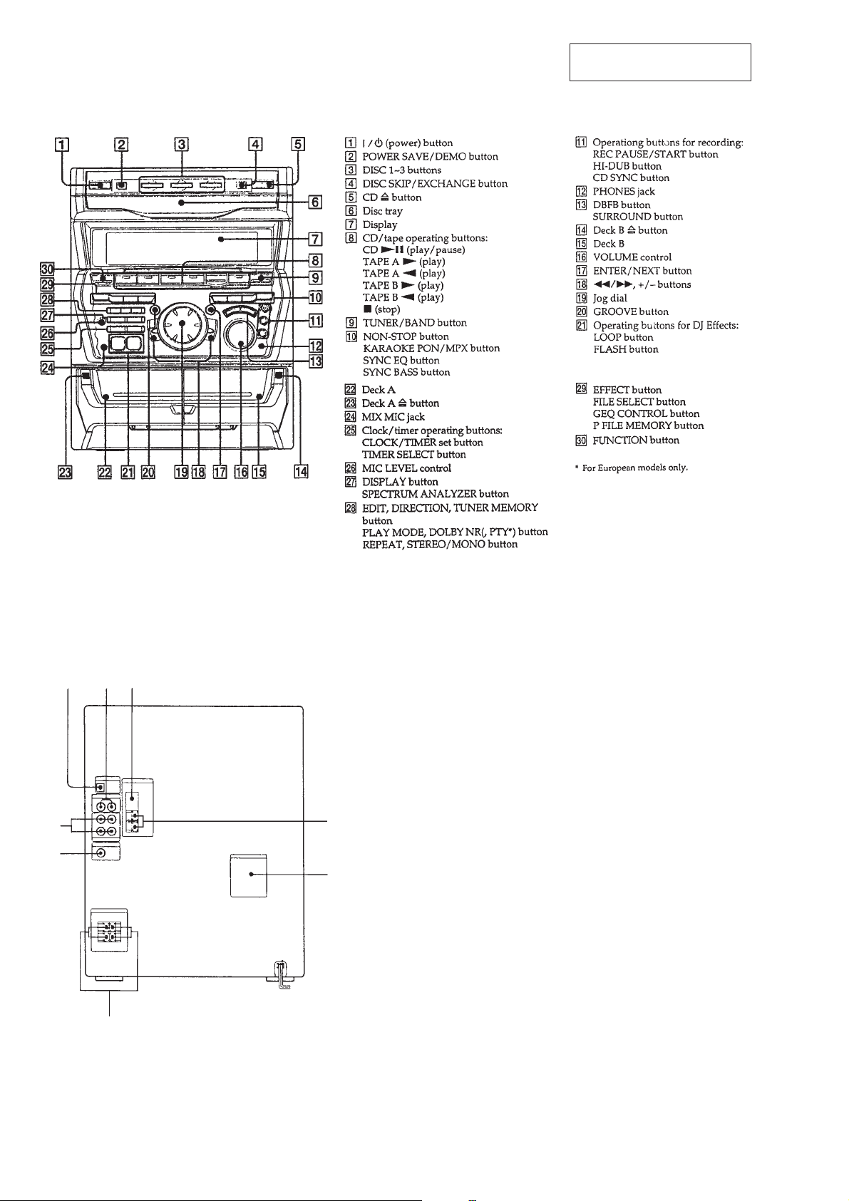
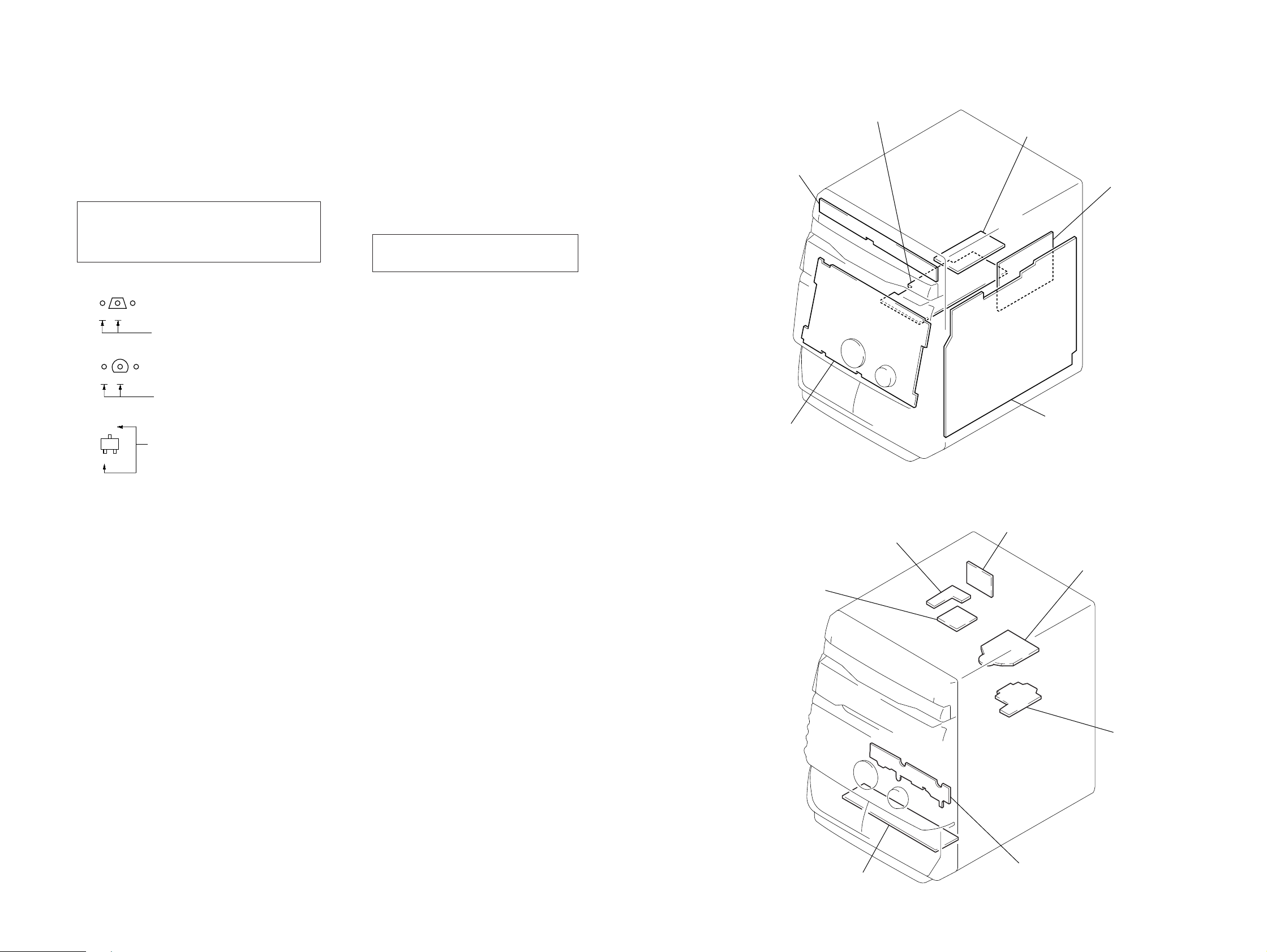
LOCATION OF CONTOROLS
– Front Panel –
SECTION 2
GENERAL
This section is extracted from
instruction manual.
– Rear Panel –
123
4
5
6
7
8
1 CD DIGITAL OUT terminal
2 VIDEO (AUDIO) IN jack
3 FM COAXIAL ANTENNA terminal
(RXD9: AEP and UK models)
FM ANTENNA terminal
(GRX9900/RXD9: US models)
4 MD IN/OUT jack
5 SUPER WOOFER jack
(GRX9900/RXD9: US models)
6 SPEAKER terminal
7 AM ANTENN A terminal
8 VOLTAGE SELECTOR switch
(GRX9900: 120 V AC Area in E, 240 V AC Area in E, Saudi
Arabia, Singapore, Malaysia, Argentine models)
– 6 –
– 7 –
SECTION 3
)
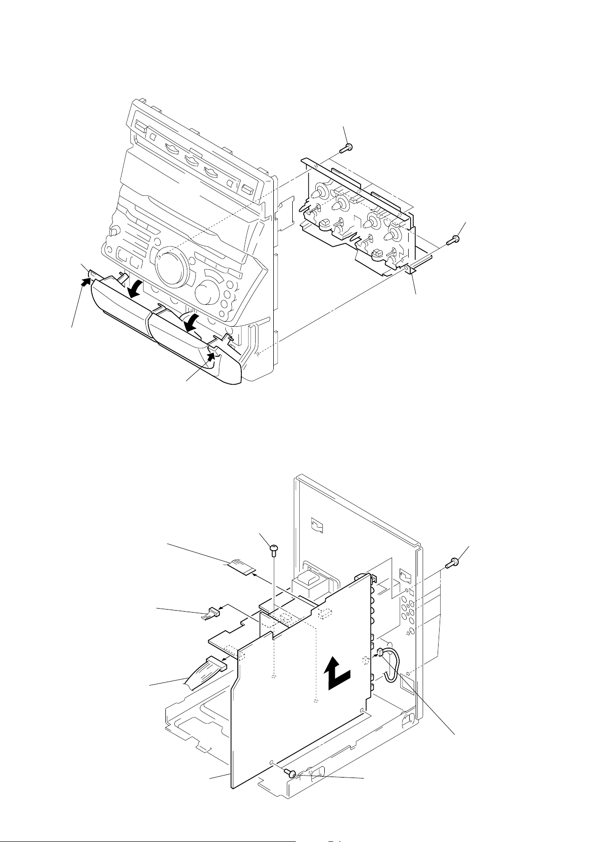
DISASSEMBLY
Note: Follow the disassembly procedure in the numerical order given.
CASE
6
case
2
screw
(case3 TP2) (3 × 12)
3
two screws
(case3 TP2) (3 × 8)
5
4
4
1
five screws
(BVTT3 × 8)
2
screw
(case3 TP2) (3 × 12)
3
two screws
(case3 TP2) (3 × 8
LOADING PANEL ASS’Y
A
1
Turn the cam-in the
direction of the arrow A.
2
Pull-out
the disc tray.
3
loading panel ass’y
– 8 –
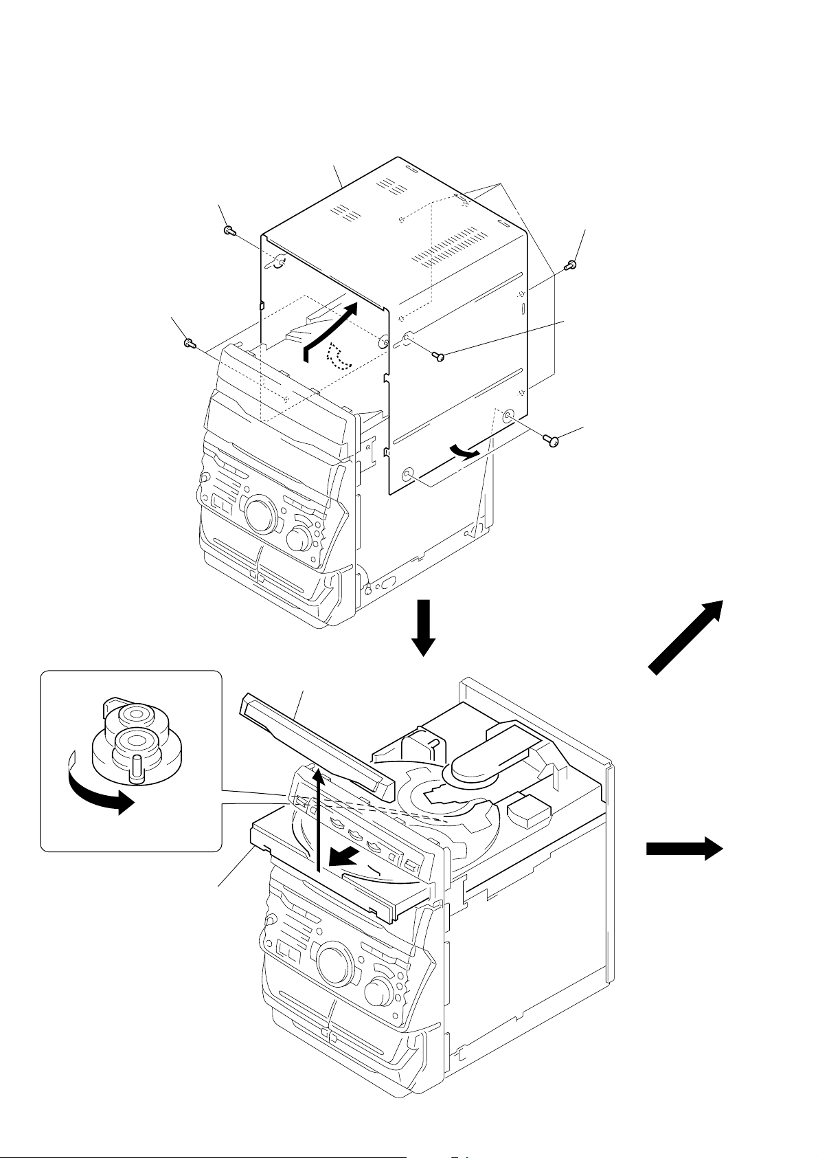
FRONT PANEL SECTION
)
5
screw
(BVTT3
×
10)
7
front panel section
1
wire (flat type)
(15 core) (32 cm) (CN303)
2
screw
(BVTT2.6
5
×
5)
screw
(BVTP3
4
lug
×
10)
1
wire (flat type)
(23 core) (CN501)
4
lug
3
two washers
2
screw
(BVTT2.6
×
5
6
three screws
×
(BVTT3
6)
CD MECHANISM DECK SECTION (CDM38LH-5BD32L)
3
Remove the CD mechanism
deck (CDM38LH-5BD32L)
in the direction of arrows
A
– B.
B
1
screw
×
(BVTP3
10)
1
wire (flat type) (17 core)
(CN304)
A
2
two screws
(BVTP3
×
8)
– 9 –
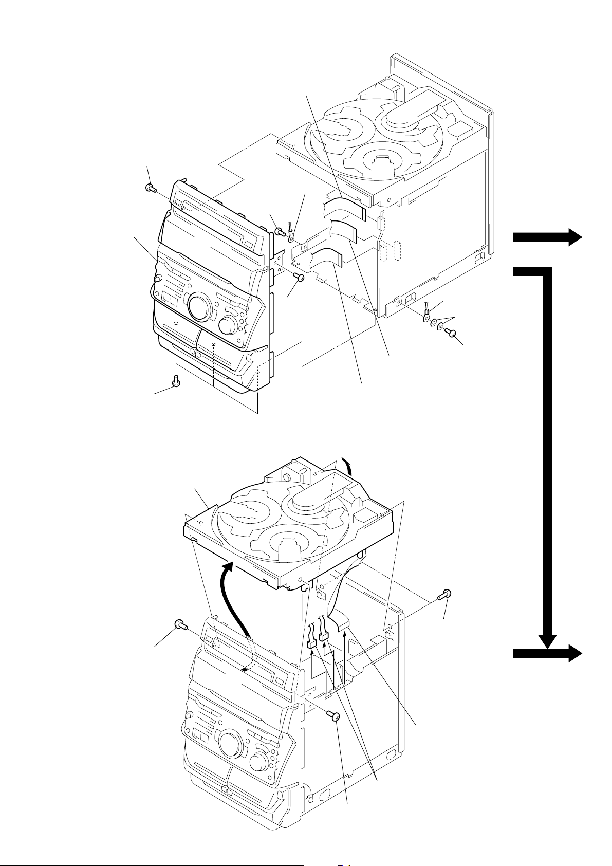
1
4
screw
(BVTP3
5
wire (flat type) (19 core)
(CN391)
two connectors
(CN392, 393)
×
10)
)
TAPE MECHANISM DECK SECTION (TCM-230AWR2)
2
Open two
cassette lids.
1
Push the cassette lid.
3
three screws
(BVTP2.6
×
8)
3
two screws
(BVTP2.6
4
tape mechanism deck
section (TCM-230AWR2)
×
8)
1
Push the cassette lid.
MAIN BOARD
• Abbreviation
AR: Argentine model
E2 : 120 V AC Area in E model
E3 : 240 V AC Area in E model
EA : Saudi Arabia model
1
wire (flat type)
13 core: GRX9900: E2, MX, AR/RXD9: US
15 core: GRX9900: E3, EA, MY, SP/
()
(CN371)
RXD9: AEP, UK
2
connector
(CN13)
(RXD9)
MX: Mexican model
MY: Malaysia model
SP : Singapore model
3
two screws
(BVTP3
×
8)
3
five screws
(BVTP3
×
8
2
connector
(CN901)
4
Remove the MAIN board
in the direction of the arrow.
– 10 –
3
two screws
(BVTP3
5
connector
(CN403)
×
8)

SECTION 4
TEST MODE
[MC Cold Reset]
• The cold reset clears all data including preset data stored in the
RAM to initial conditions. Execute this mode when returning
the set to the customer.
Procedure:
1. Turn the power ON or set to the DEMO mode.
2. Press three buttons of p , [ENTER/NEXT], and 1/u simulta-
neously.
3. The set is reset, and displays “COLD RESET”, then becomes
DEMO mode.
[MC Hot Reset]
• This mode resets the set with the preset data kept stored in the
memory. The hot reset mode functions same as if the power
cord is plugged in and out.
Procedure:
1. Turn the power ON or set to the DEMO mode.
2. Press three buttons of p , [ENTER/NEXT], and [DISC1] si-
multaneously.
3. The set is reset, and becomes standby state.
[Change-over the AM Tuning Interval]
(EXCEPT AEP, UK, and Saudi Arabia models)
• The AM tuning interval can be changed over 9 kHz or 10 kHz.
Procedure:
1. Press the 1/u button to turn the power ON.
2. Select the function “TUNER”, and press the [TUNER/BAND]
button to select the BAND “AM”.
3. Press the 1/u button to turn the power OFF.
4. Press the [ENTER/NEXT] and 1/u buttons simultaneously,
and the display on the fluorescent indicator tube changes to
“AM 9 k STEP” or “AM 10 k STEP”, and thus the tuning
interval is changed over.
[CD Service Mode]
• This mode can run the CD sled motor optionally. Use this mode,
for instance, when cleaning the optical pick-up.
Procedure:
1. Press the 1/
2. Select the function “CD”.
3. Press three buttons of p , [ENTER/NEXT], and § simulta-
neously.
4. Set to the Sled Servo mode.
5. With the CD in stop status, turn the JOG dial clockwise to
move the optical pick-up to outside track, or turn it counterclockwise to inside track.
6. To exit from this mode, perform as follows.
1) Move the optical pick-up to the most inside track.
2) Disconnect the power cord.
Notes: • Always move the optical pick-up to most inside track when
u button to turn the power ON.
exiting from this mode. Otherwise, a disc will not be unloaded.
• Do not r un the sled motor excessively, otherwise the gear can
be chipped.
[CD Delivery Mode]
• This mode moves the optical pick-up to the position durable to
vibration. Use this mode when returning the set to the customer
after repair.
Procedure:
1. Press the 1/
2. Press the [LOOP] and 1/u buttons simultaneously.
3. A message “LOCK” is displayed on the fluorescent indicator
tube, and the CD delivery mode is set.
[LED and Fluorescent Indicator Tube All Lit, Key Check
Mode]
Procedure:
1. Press three buttons of p , [ENTER/NEXT], and [DISC2] si-
multaneously.
2. LEDs and fluorescent indicator tube are all turned on.
Press the [DISC2] button, and the key check mode is activated.
3. In the key check mode, the fluorescent indicator tube displays
“K 0 J0 V0”. Each time a button is pressed, “K” value increases. However , once a button is pressed , it is no longer taken
into account.
“J” value increases like 1, 2, 3 ... if turn the JOG dial clockwise, or it decreases like 0, 9, 8 ... if turn the JOG dial counterclockwise.
“V” value increases like 1, 2, 3 ... if turn the [VOLUME] dial
clockwise, or it decreases like 0, 9, 8 ... if turn the JOG dial
counterclockwise.
4. To exit from this mode, press three buttons in the same man-
ner as step 1, or disconnect the power cord.
u button to turn the power ON.
– 11 –
[Aging Mode]
This mode can be used for operation check of CD section and tape
deck section.
CD section and tape deck section work in parallel.
• If an error occurred:
The aging operation stops only an error occurred sections and
display then status.
• If no error occurs:
The aging operation continues repeatedly.
Procedure:
1. Set disc in DISC1 tray.
2. Load the tapes into the decks A and B respectively.
3. Press the [PLAYMODE] button to set the “ ALL DISCS” mode,
and press the [REPEAT] button to “REPEAT” off.
4. Press the [FUNCTION] button to select the function “CD”.
5. Press three buttons of p , [ENTER/NEXT], and [DISCSKIP/
EX-CHANGE] simultaneously.
6. The aging mode is activated, if the indicator of disc tray num-
ber on the fluorescent indicator tube is blinking.
7. To exit from the aging mode, press the 1/u button to turn the
power OFF and operate the cold reset. (Refer to the “MC Cold
Reset”)
• Display at an error occurred
1) Display of the error count
(1) Press three buttons of p , [ENTER/NEXT], and [CDSYNC]
simultaneously.
(2) Display of the error count following as below.
Display
EMC**EDC
Notes:
EMC**: The number of mechanical error.
EDC**: The number of no disc error after chucking the disc.
**
2) Display of mechanical error
Display
E**M##$$&&
1. Display at the Aging Mode
• Display operating state of CD section and tape deck section alternately.
• If an error occurred, stop display which that section.
2. CD Section
• Display at the aging mode is the same as the normal operation.
• T he sequence during the aging mode is following as below.
Aging mode sequence (CD section) :
Turn the disc tray
Disc1 chucking
TOC read
Play track1 for 2 seconds
Play last track for 2 seconds
Notes:
: The number of mechanical error.(“00” is latest one)
**
(Press the [PLAYMODE] button to changes next error display)
## : Not used.
$$ : Loading error. (Second figure is not used)
D: The error in the midst of close at the except mechanical trouble.
E : The error in the midst of open at the except mechanical trouble.
C : The error in the midst of chuck up at the except mechanical
trouble.
F : The error in the midst of EX-open at the except mechanical
trouble.
&&: Loading error. (Second figure in not used)
1:The error in the midst of chuck up.
2:The error in the midst of chuck down.
3:Time up of EX-open
4:Time up of EX-close.
3) Display of no disc error
Display
E**D##$$&&
Notes:
: The number of mechanical error.(“00” is latest one)
**
(Press the [REPEAT] button to changes next error display)
##:
01:Focus error
02:GFS error
03:Set up error
$$:
00:No disc error when does not chucking retry.
02:No disc error when chucking retry to completion.
&&: The state when judged no disc error. (Second figure is not used)
1: Stop
2: Set up
3: TOC read
4: Access
5: Play
6: Pause
7: Manual search (Play)
8: Manual search (Pause)
– 12 –
3. Tape Deck Section
• The sequence during the aging mode is following as below.
• If an error occurred, stop display that step.
Aging mode sequence (Tape deck section) :
Rewind the tape A and B
“TAPE A AG-1”
Shut off
FWD play the tape A
“TAPE A AG-2”
2 minutes
Fast forward the tape A
“TAPE A AG-3”
Shut off or 20 seconds
REV play the tape A
“TAPE A AG-4”
2 minutes
Rewind the tape A
“TAPE A AG-5”
Shut off
FWD play the tape B
“TAPE B AG-2”
2 minutes
Fast forward the tape B
“TAPE B AG-3”
Shut off or 20 seconds
REV play the tape B
“TAPE A AG-4”
2 minutes
Rewind the tape B
“TAPE B AG-5”
Shut off
Note: “TAPE * AG-*” is display of each step.
– 13 –
SECTION 5
r
MECHANICAL ADJUSTMENTS
SECTION 6
ELECTRICAL ADJUSTMENTS
Precaution
1. Clean the following parts with a denatured alcohol-moistened
swab:
record/playback heads pinch rollers
erase head rubber belts
capstan idlers
2. Demagnetize the record/playback head with a head demagnetizer.
3. Do not use a magnetized screwdriver for the adjustments.
4. After the adjustments, apply suitable locking compound to the
parts adjusted.
5. The adjustments should be performed with the rated power supply voltage unless otherwise noted.
Torque Measurement
Mode
FWD
FWD
back tension
REV
REV
back tension
FF/REW
FWD tension
REV tension
Torque meter
CQ-102C
CQ-102C
CQ-102RC
CQ-102RC
CQ-201B
CQ-403A
CQ-403R
Meter reading
31 to 71 g • cm
(0.43 – 0.98 oz • inch)
2 to 6 g • cm
(0.03 – 0.08 oz • inch)
31 to 71 g • cm
(0.43 – 0.98 oz • inch)
2 to 6 g • cm
(0.03 – 0.08 oz • inch)
71 to 143 g • cm
(0.99 – 1.99 oz • inch)
100 g or more
(3.53 oz or more)
100 g or more
(3.53 oz or more)
DECK SECTION
0 dB=0.775 V
1. Demagnetize the record/playback head with a head demagnetizer.
2. Do not use a magnetized screwdriver for the adjustments.
3. After the adjustments, apply suitable locking compound to the
parts adjust.
4. The adjustments should be performed with the rated power
supply voltage unless otherwise noted.
5. The adjustments should be performed in the order given in
this service manual. (As a general rule, playback circuit adjustment should be completed before performing recording
circuit adjustment.)
6. The adjustments should be performed for both L-CH and RCH.
7. Switches and controls should be set as follows unless otherwise specified.
8. Set to the DOLBY NR OFF.
9. Set to the test mode.
(1) Press the 1/u button to turn the power ON.
(2) Select the function “TAPE A or B”.
(3) Press the button of p , [ENTER/NEXT], and [DISC3]
simultaneously, to set the tape deck test mode and blink
the indicator of disc tray number on the fluorescent indicator tube.
(4) To exit from the test mode, press the 1/u button.
• Test Tape
Tape Signal Used for
P-4-A100 10 kHz, –10 dB Azimuth Adjustment
WS-48B 3 kHz, 0 dB Tape Speed Adjustment
P-4-L300 315 Hz, 0 dB Level Adjustment
Record/Playback Head Azimuth Adjustment
DECK A DECK B
Note: Perform this adjustments for both decks
Procedure:
1. Mode: Playback
test tape
P-4-A100
(10 kHz, –10 dB)
MAIN board
MD OUT jack (J101)
L-CH, R-CH
set
level mete
+
–
– 14 –
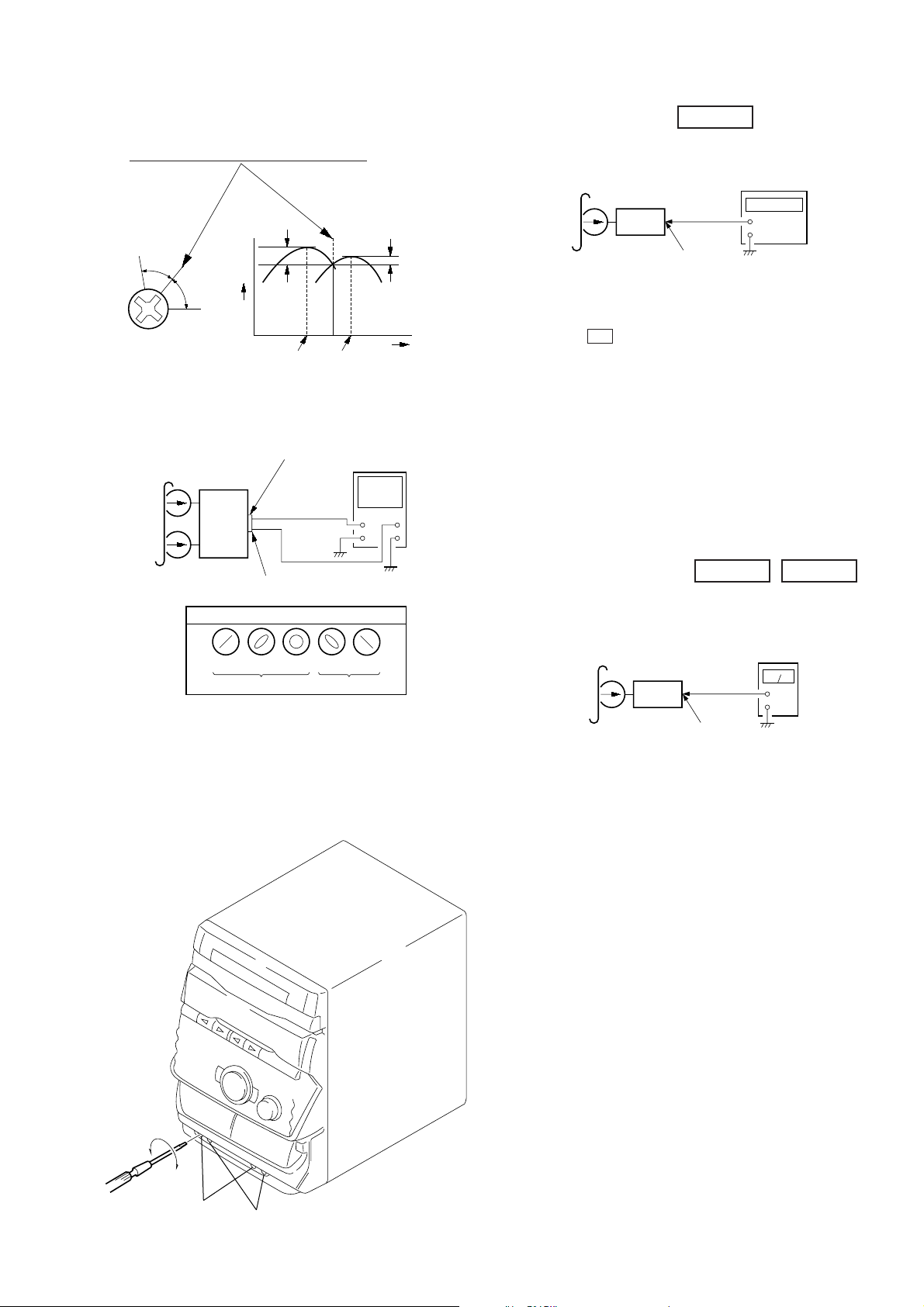
2. T urn the adjustment scre w and check output peaks. If the peaks
do not match for L-CH and R-CH, turn the adjustment screw
so that outputs match within 1dB of peak.
Tape Speed Adjustment
Mode: Playback
test tape
WS-48B
(3 kHz, 0 dB)
DECK B
frequency counter
Output
level
within
1dB
L-CH
peak
R-CH
peak
within
1dB
Screw
position
L-CH
peak
Screw
position
R-CH
peak
3. Mode: Playback
MAIN board
test tape
P-4-A100
(10 kHz, –10 dB)
L-CH
R-CH
in phase 45°90°135°180
MD OUT jack (J101)
L-CH
R-CH
waveform of oscilloscope
good
oscilloscope
wrong
H
V
°
4. Repeat step 1 to 3 in playback (REV) mode.
5. After the adjustments, apply suitable locking compound to the
pats adjusted.
set
MAIN board
MD OUT jack (J101)
L-CH, R-CH
+
–
1. Insert the WS-48B into the deck B.
2. Press the ( button on the deck B.
3. Press the [HI-DUB] button in playback mode.
Then at HIGH speed mode.
4. Adjust RV1001 on the LEAF SW board do that frequency
counter reads 6,000 ± 180 Hz.
5. Press the [HI-DUB] button.
Then back to NORMAL speed mode.
6. Adjust RV1002 on the LEAF SW board so that frequency
counter reads 3,000 ± 90 Hz.
Adjustment Location: LEAF SW board
Sample value of Wow and Flutter: 0.3% or less W.RMS (JIS)
(WS-48B)
Playback level Adjustment DECK A DECK B
Procedure:
Mode: Playback
test tape
P-4-L300
(315 Hz, 0 dB)
set
MAIN board
MD OUT jack (J101)
L-CH, R-CH
level meter
+
–
Adjustment Location:Playback Head (Deck A).
Record/Playback/Earth Head (Deck B).
forward
reverse
Deck A is RV311 (L-CH) and RV411 (R-CH), Deck B is RV301
(L-CH) and RV401 (R-CH) so that adjustment within adjustment
level as follows.
Adjustment Level:
J101 PB level: 301.5 to 338.3 mV (–8.2 to –7.2 dB) level
difference between the channels: within ±0.5 dB
Adjustment Location: AUDIO board
– 15 –
REC Bias Adjustment DECK B
Procedure:
1. Mode: Record
FUNCTION: VIDEO
MAIN board
VIDEO (AUDIO) IN jack (J101)
L-CH, R-CH
50 mV (–23.8 dB)
600
Ω
AF OSC
1) 315 Hz
2) 10 kHz
attenuator
2. Mode: Playback
set
blank tape
CN-123
Specification values:
J101 PB level: 47.2 to 53.0 mV (–24.3 to –23.3 dB)
Adjustment Location: MAIN board
– MAIN BOARD (Conductor Side) –
RV301
L
IC301
RV351
R
REC LEVEL
VIDEO (AUDIO) IN
J101
MD OUT
(L/R)
(L/R)
recorded
portion
set
MAIN board
MD OUT jack (J101)
L-CH, R-CH
level meter
+
–
3. Confirm playback the signal recorded in step 1 become specification values as follows.
If these values are out of specification values, adjust the R V341
(L-CH) and RV441 (R-CH) on the AUDIO board to repeat
steps 1and 2.
Specification values: Playback output of 315 Hz to playback
output of 10 kHz: ± 0.5 dB
Adjustment Location: AUDIO board
REC Level Adjustment DECK B
Procedure:
1. Mode: Record
FUNCTION: VIDEO
MAIN board
VIDEO (AUDIO) IN jack (J101)
L-CH, R-CH
AF OSC
315 Hz, 50 mV (–23.8 dB)
Ω
attenuator
600
blank tape
CS-123
set
– AUDIO BOARD (Component Side) –
RV441
RV401
RV301
LR
PB LEVEL
– DECK B –
– LEAF SW BOARD (Component Side) –
TAPE SPEED
(NORMAL) (HIGH)
RV1002
RV1001
IC602
RV341
RL
REC BIAS
CN601
CN1001
RV311
LR
PB LEVEL
– DECK A –
RV411
2. Mode: Playback
recorded
portion
set
MAIN board
MD OUT jack (J101)
L-CH, R-CH
level meter
+
–
3. Confirm playback the signal recorded in step 1 become specification values as follows.
If these values are out of specification values, adjust the R V301
(L-CH) and R V351 (R-CH) on the MAIN board to repeat steps
1 and 2.
– 16 –
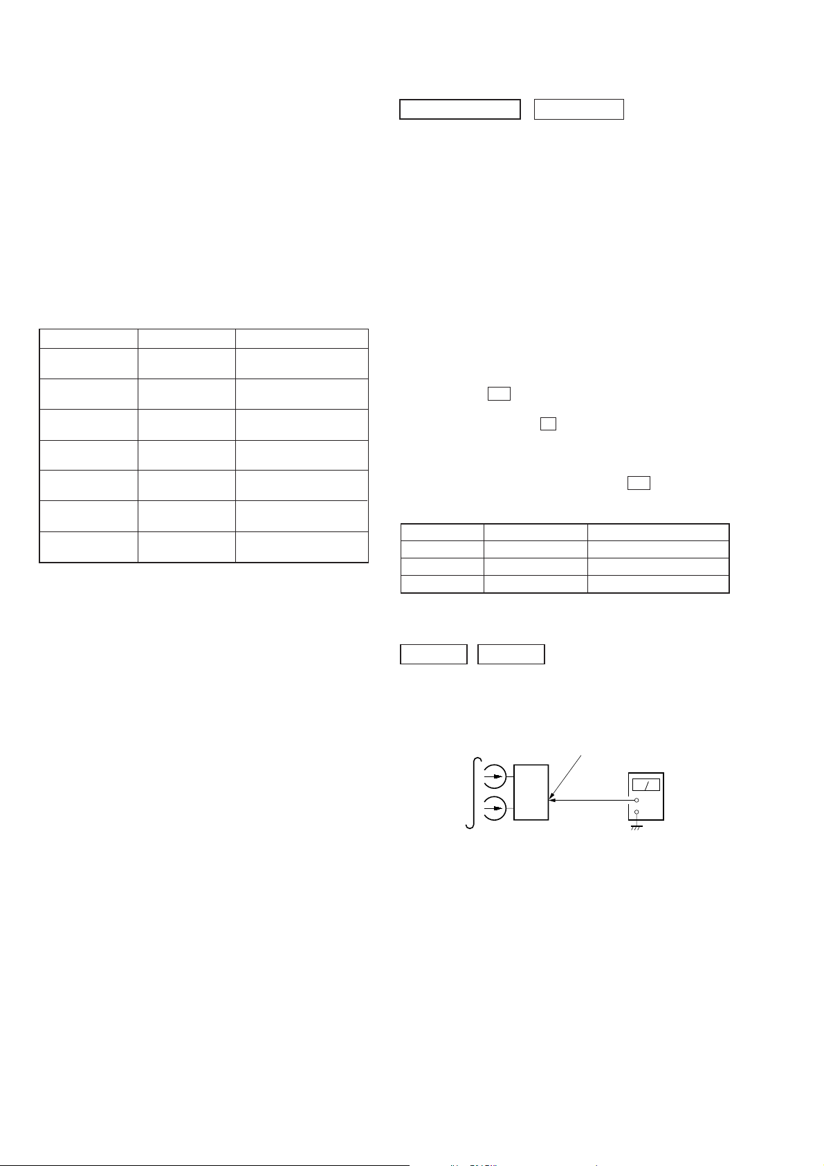
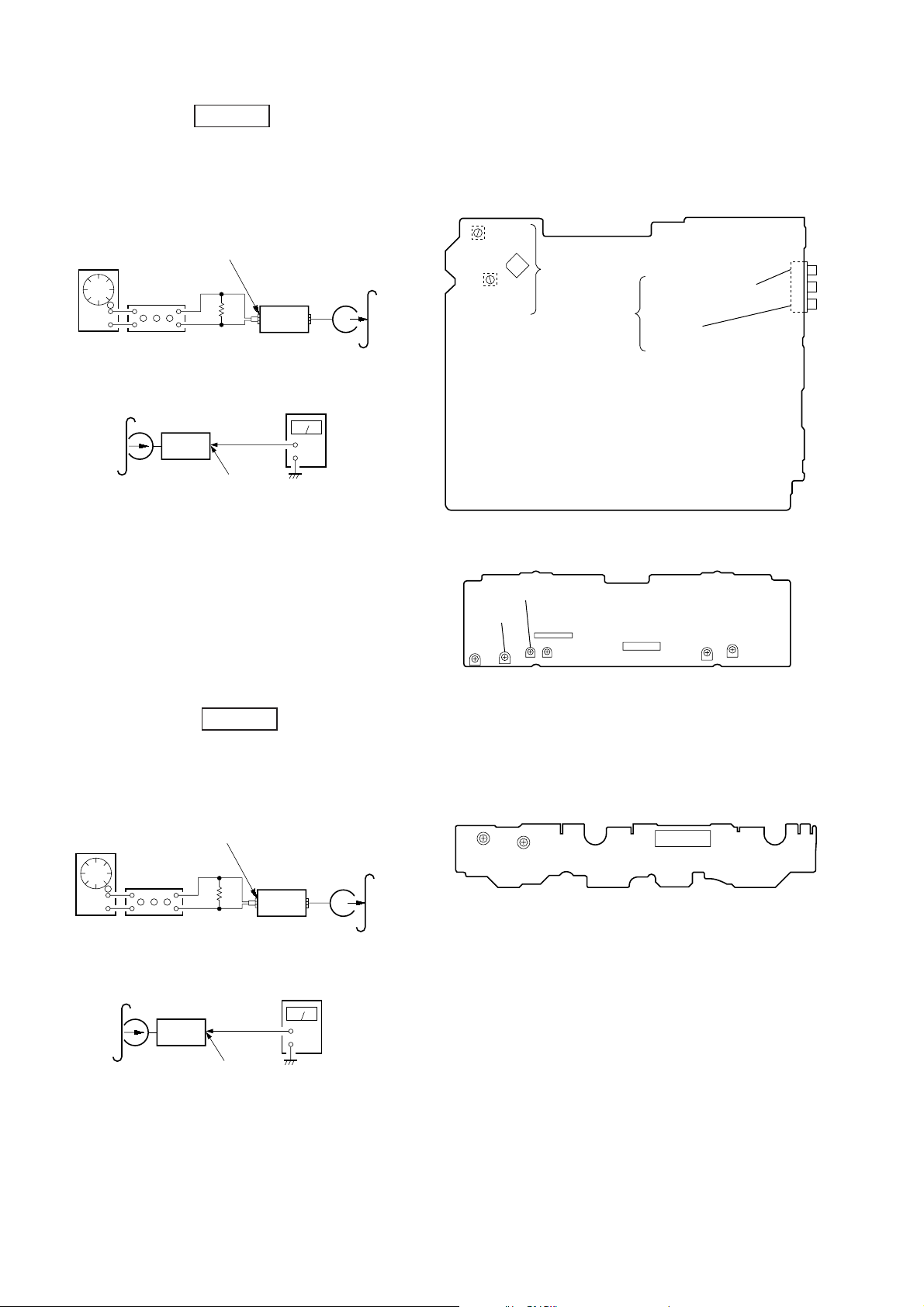
CD SECTION
V
+
–
BD board
TP (TE)
TP (VC)
oscilloscope
)
Note:
1. CD Block is basically designed to operate without adjustment. Therefore, check each item in order given.
2. Use YEDS-18 disc (3-702-101-01) unless otherwise indicated.
3. Use an oscilloscope with more than 10 MΩ impedance.
4. Clean the object lens by an applicator with neutral detergent when the
signal level is low than specified value with the following checks.
S-Curve Check
oscilloscope
BD board
TP (FE)
TP (VC)
+
–
E-F Balance (1 Track Jump) Check
Procedure :
1. Connect oscilloscpe to TP (TE) and TP (VC).
2. Turn the power ON.
3. Load a disc (YEDS-18) and playback the number five track.
4. Press the ^ (CD) button. (Becomes the 1 track jump mode)
5. Confirm that the level B and A (DC voltage) on the oscilloscope waveform.
Procedure:
1. Connect oscilloscope to TP (FE).
2. Connect between TP (FE1) and TP (VC) by lead wire.
3. Connect between TP (AGCCON) and TP (GND) by lead wire.
4. Turn the power ON.
5. Load a disc (YEDS-18) and actuate the focus search. (In consequence of open and close the disc tray, actuate the focus
search)
6. Cofirm that the oscilloscope waveform (S-curve) is symmetrical between A and B. And confirm peak to peak level within
4 ± 1 Vp-p.
S-curve waveform
symmetry
A
B
within 4
±
1 Vp-p
7. After check, remove the lead wire connected in step 2 and 3.
Note: • Try to measure several times to make sure than the ratio of A : B
or B : A is more than 10 : 7.
• Take sweep time as long as possible and light up the brightness
to obtain best waveform.
RF Level Check
oscilloscope
BD board
1 track jump waveform
B
0V
level = 1.3
Specified level: × 100 = less than ± 22%
±
0.6 Vp-p symmetry
A
B
A (DC voltage
6. After check, remove the lead wire connected in step 1.
center of
waveform
TP (RF)
TP (VC)
+
–
Procedure:
1. Connect oscilloscope to TP (RF).
2. Connect between TP (AGCCON) and TP (GND) by lead wire.
3. Turn the power ON.
4. Load a disc (YEDS-18) and playback.
5. Confirm that the oscilloscope waveform is clear and check RF
signal level is correct or not.
6. After check, remove the lead wire connected in step 2.
Note: Clear RF signal waveform means that the shape “≈” can be clearly
distinguished at the center of the waveform.
VOLT/DIV: 200 m
TIME/DIV: 500 ns
level:
±
0.3 Vp-p
1.45
– 17 –
Checking Location:
– BD BOARD (Side B) –
TP (VC)
TP (RF)
IC103
IC102
TP (TE)
TP (GND)
TP
(AGCCON)
TP (FE)
TP (FE1)
– 18 –
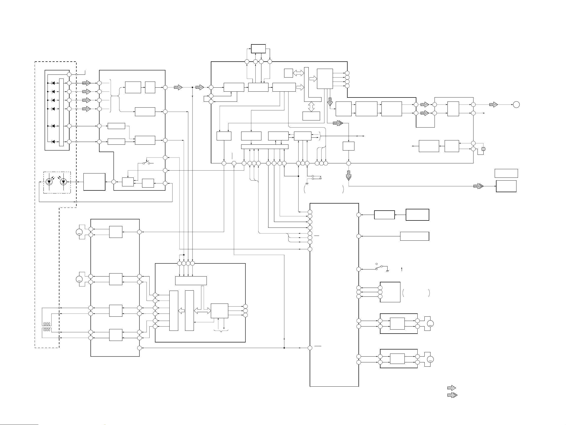
SECTION 7
DIAGRAMS
7-1. BLOCK DIAGRAM – CD SERVO Section –
HCD-GRX9900/RXD9
DETECTOR
A
B
C
D
F
E
OPTICAL PICK-UP
(KSS-213D/Q-NP)
LASER DIODE
PD
7
4
2
1
5
I-V AMP
10
6
LD
CD D+5V
10
11
AUTOMATIC
POWER
CONTROL
Q101
FOCUS/TRACKING ERROR AMP
A
5
B
6
C
7
D
8
F
F I-V AMP
E
E I-V AMP
LD
3
RF AMP,
SUMMING
APC LD
AMP
IC103
RF
AMP
RF EQ
AMP
FOCUS
ERROR AMP
TRACKING
ERROR AMP
APC PD
AMP
RFO
HOLD SW
LDON
FILTER
53
54 56
FILO
PCO
CLTV
RFAC
ASYI
ASYO
DIGITAL
CLV
MDP
26
ASYMMETRY
CORRECTION
XRST
3
16
FE
14
TE
13
21
22
PD
4
51
49
48
DIGITAL
SUBCODE
PROCESSOR
XLON
XLAT
DATA
14 5 6
PLL
CPU INTERFACE
CLOK
SENS
8
7
DIGITAL SIGNAL PROCESSOR,
DIGITAL FILTER, D/A CONVERTER
55
FILI
EFM
DEMODULATOR
SERVO AUTO
SEQUENCER
SQSO
SCOR
20
1 2
16K
RAM
SQCK
IC101 (1/2)
CORRECTOR
SERVO
INTERFACE
SCLK
COUT
9 21
D/A
INTERFACE
INTERNAL BUS
ERROR
SSTP
EMPH
WFCK
GFS
64 15
27
ON :
18
S101
(LIMIT)
When the optical pick-up
is inner position.
PCMD
BCK
LRCK
C2PO
SERIAL
IN
INTERFACE
DIGITAL
62
63
61
19
OUT
DOUT
60
DIGITAL
FILTER,
NOISE SHAPER
TO MIRR/DFCT/
FOK DETECTOR
PWM
&
INTEGRATOR
AOUT1
AOUT2
70
77
CLOCK
GENERATOR
X101
CD DIGITALOUT
OPTICAL
OPTICAL
TRANSCEIVER
CD-L
IC381
IC381
A
(Page 23)
BUFFER
TIMING
LOGIC
LOUT1
LOUT2
XTAI
XTAO
72
75
R-CH
66
67
16.9344MHz
AIN1
71
AIN2
76
(TRACKING)
(FOCUS)
05
2-AXIS
DEVICE
M101
(SPINDLE)
M102
(SLED)
FOCUS/TRACKING COIL DRIVE,
SPINDLE/SLED MOTOR DRIVE
IC102
CH4OUTF
15
M
M
16
17
18
12
11
14
13
CH4OUTR
CH3OUTF
CH3OUTR
CH2OUTF
CH2OUTR
CH1OUTF
CH1OUTR
MOTOR
DRIVE
MOTOR
DRIVE
COIL
DRIVE
COIL
DRIVE
CH4SIN
CH3FIN
CH3RIN
CH2FIN
CH2RIN
CH1FIN
CH1RIN
MUTE
25
43
39
40
41
FE
TE
SE
24
23
SFDR
28
SRDR
29
5
6
2
3
20
TFDR
30
TRDR
31
FFDR
32
33
FRDR
FOCUS/TRACKING/SLED
RFDC
A/D
CONVERTER
PWM GENERATOR
SERVO DSP
FOCUS/TRACKING/SLED
DIGITAL SERVO
PROCESSOR
IC101 (2/2)
MIRR/DFCT/
FOK
DETECTOR
TO SERVO INTERFACE
FOK
MIRR
DFCT
24
22
23
33
SQ-CLK
32
SQ-DATA
19
SCOR
56
SENSE
37
CD-CLK
58
XLT
CD-DATA
35
HOLD
57
SYSTEM CONTROLLER
(CD MECHANISM CONTROL)
IC501 (1/4)
59
XRST
DISC-SENS
TBL-SENS
OUT-OPEN
ENC1
ENC2
ENC3
LOAD-OUT
LOAD-IN
TBL-L
TBL-R
60
61
71
69
68
66
67
63
65
LEVEL SHIFT
Q701
(OPEN/CLOSE DET)
470
ROTARY
2
ENCODER
S811
3
DISC TRAY SLIDE MOTOR DRIVE
FIN
10
RIN
2
DISC TRAY TURN MOTOR DRIVE
IN1
3
IN2
6
DISC TRAY SENSOR
S801
CLOSE
OPEN
IC801
MOTOR
DRIVE
IC701
MOTOR
DRIVE
DISC IN DETECT
SENSOR
IC703
IC702
DISC TRAY
ADDRESS DETECT
OUT1
7
OUT2
4
OUT1
7
OUT2
2
M
(DISC TRAY SLIDE)
M
(DISC TRAY TURN)
M801
M701
– 19 – – 20 –
• SIGNAL PATH
: CD PLAY (ANALOG OUT)
: CD PLAY (DIGITAL OUT)
HCD-GRX9900/RXD9
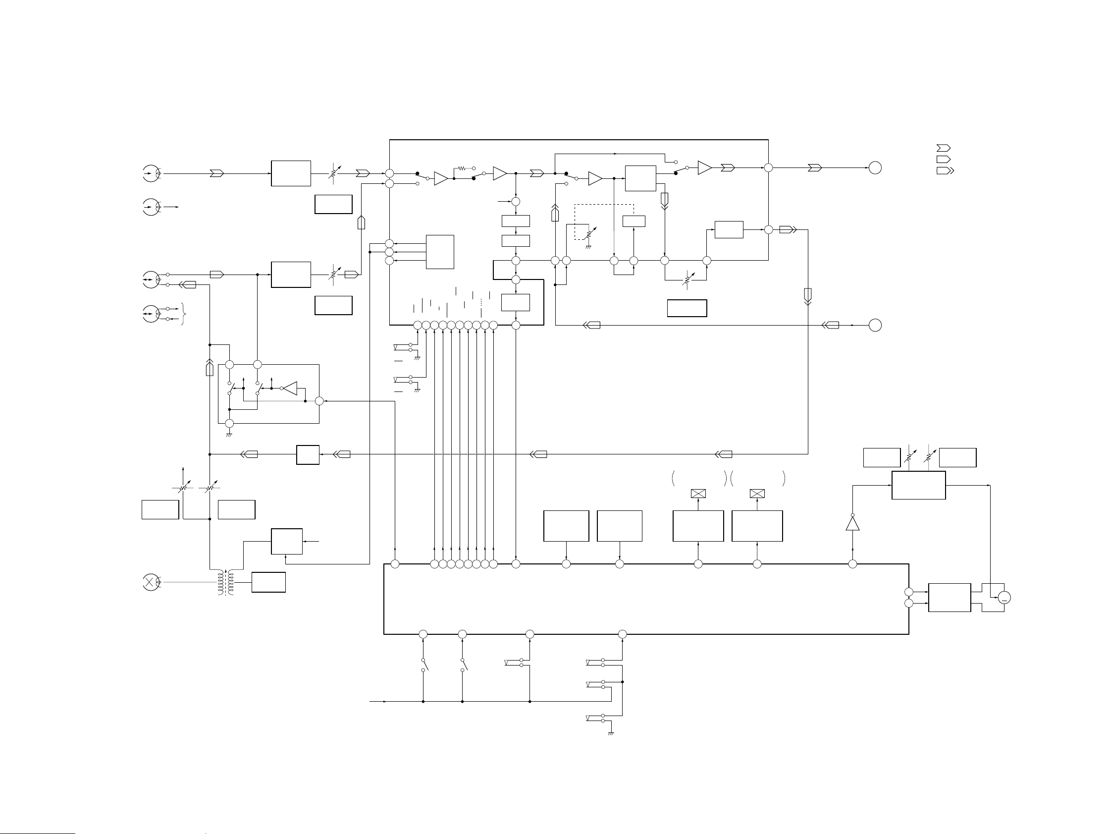
7-2. BLOCK DIAGRAM – TAPE DECK Section –
L-CH
R-CH R-CH
(RECORD/PLAYBACK)
L-CH
R-CH R-CH
HP101
(PLAYBACK)
HRPE101 (1/2)
DECK PROCESS
DECK A/B SELECT, PB/REC EQ AMP,
DOLBY NR AMP, ALC, AMS
IC301
DOLBY PASS
NORM/HIGH
PB A/B
70
120
R-CH
NR ON/OFF
BIAS ON/OFF
RM ON/OFF
L.P.F.
BUFFER
AMS
CIRCUIT
REC/PB/PASS
LM ON/OFF
+
28
27
26
MAOUT
MSIN
MSOUT
RIN (L)
43
ALC (L)
44
DOLBY NR
ALC
ALC
ROUT (L)
35 34
AMP
CIRCUIT
IN (L)
REC OUT (L)
39
RV301
REC LEVEL (L)
(DECK B)
EQ IN (L)
38
PB EQ AMP
(DECK A)
IC611
PB EQ AMP
(DECK B)
IC601
REC/PB SWITCHING
IC602
1
3
R-CH
R-CH
RV311
PB LEVEL (L)
(DECK A)
RV301
PB LEVEL (L)
(DECK B)
4
AIN (L)
48
BIN (L)
46
BIAS (N)
33
BIAS (C)
32
BIAS (M)
31
S1004
(DECK A 120/70)
S1008
(DECK B 120/70)
BIAS
CONTROL
CIRCUIT
B NORM/CROM
ALC ON/OFF
A 120/70
1516182022 23242517
19
REC
EQ AMP
PB OUT (L)
EQ OUT
40
(L)
36
PB-L
REC-L
B
(Page 23)
C
(Page 24)
• SIGNAL PATH
: PLAYBACK (DECK A)
: PLAYBACK (DECK B)
: RECORD
RV441
REC BIAS (R)
(DECK B)
HRPE101 (2/2)
(ERASE)
R-CH
05
2
RV341
REC BIAS (L)
(DECK B)
BIAS OSC
T621
BIAS OSC
Q621, 622
REC BIAS
SWITCH
Q623
C331, L331
BIAS
TRAP
B+
(A+7V)
D+5V
100
TC-RELAY
(DECK A PLAY)
8584838281 807978
PB-A/B
EQ-H/N
ALC-ON/OFF
A-PLAY-SW
87
S1001
S1002
(DECK B PLAY)
BIAS
REC-MUTE
B-PLAY-SW
86
TC-MUTE
R/P-PASS
NR-ON/OFF
(DECK A HALF)
S1003
77
AMS-IN
88
DETECT SENSOR
A-HALF
(DECK B HALF)
(DECK A REC)
ROTATION
(DECK A)
IC1001
91
A-SHUT
S1006
S1005
S1009
(DECK B REC)
ROTATION
DETECT SENSOR
(DECK B)
IC1002
90
B-SHUT
SYSTEM CONTROLLER
B-HALF
89
IC501 (2/4)
TRIGGER PLUNGER
DECK A
TRIGGER
PLUNGER DRIVE
(DECK A)
Q333, 334
73
A-TRG
TRIGGER PLUNGER
DECK B
TRIGGER
PLUNGER DRIVE
(DECK B)
Q331, 332
72
B-TRG
Q335
76
CAP-M-H/L
RV1001
TAPE SPEED
(HIGH)
CAPM-CNT1
CAPM-CNT2
CAPSTAN MOTOR
CONTROL SWITCH
Q1001
75
MOTOR DRIVE
74
RV1002
TAPE SPEED
(NORMAL)
CAPSTAN
Q336 – 343
M
M1
(CAPSTAN)
– 21 –
– 22 –
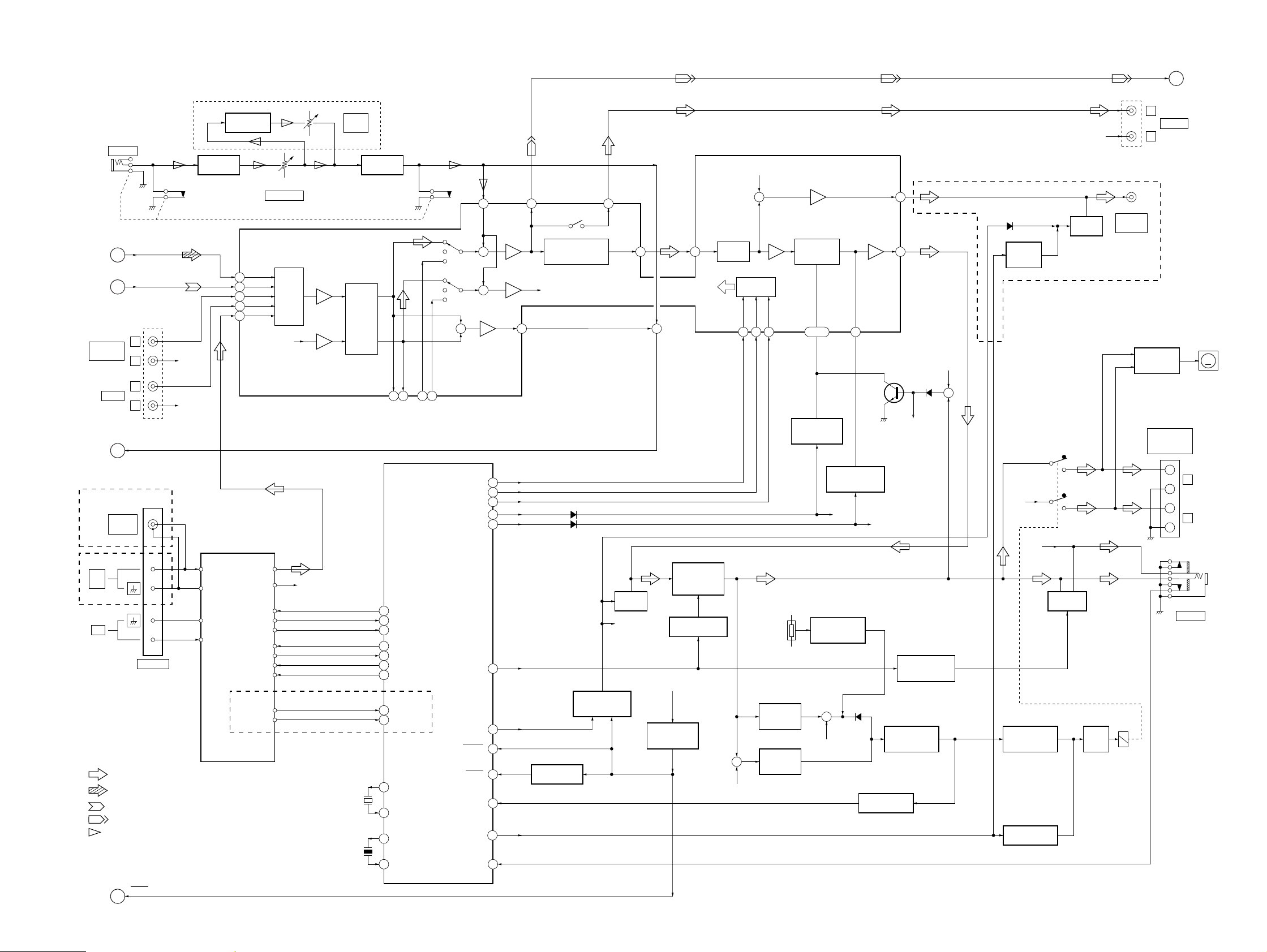
7-3. BLOCK DIAGRAM – MAIN Section –
HCD-GRX9900/RXD9
J711
MIX MIC
VIDEO
MD IN
A
B
D
FM 75Ω
COAXIAL
CD-L
PB-L
SPEANA
(Page 20)
(Page 22)
(AUDIO) IN
(Page 25)
(RXD9: AEP, UK)
(GRX9900/RXD9: US)
FM
75Ω
AM
• SIGNAL PATH
: TUNER (FM/AM)
: CD PLAY
: TAPE PLAY
: RECORD
: MIC INPUT
(Page 25)
RESET
E
J101 (1/2)
L
R
L
R
ANTENNA
R-CH
R-CH
MIC AMP
IC712 (1/2)
(GRX9900: Saudi Arabia)
DIGITAL ECHO
IC711
IN E2
65
IN D2
66
IN B2
68
IN A2
69
IN C2
67
GRAPHIC EQUALIZER CONTROL,
FM/AM TUNER UNIT
FM ANT
FM ANT
AM ANT
AM ANT
ST-L
ST-R
ST-MUTE
STEREO
TUNED
ST-DIN
ST-DOUT
ST-CLK
ST-CE
RDS-DATA
RDS-INT
RV712
MIC LEVEL
INPUT
SELECT
SWITCH
R-CH
INPUT SELECT SWITCH,
ELECTRICAL VOLUME
IC101
R-CH
(RXD9: AEP, UK)
05
RV711
ECHO
LEVEL
SOUND
CONTROL
CIRCUIT
X601
32.768kHz
X613
16MHz
MIC AMP
IC712 (2/2)
49
50
51
53
54
55
52
21
20
11
10
13
15
KEY IN2
KEY IN1
KEY OUT 2
60 5 59 6
SYSTEM CONTROLLER
ST-MUTE
STEREO
TUNED
ST-DOUT
ST-DIN
ST-CLK
ST-CE
RDS-DATA
RDS-INT
XC-OUT
XC-IN
X-OUT
X-IN
KEY OUT 1
IC501 (3/4)
PROTECTOR
2 58 57
MIC IN
REC A2
+
+
L+R
+
493-DATA
493-CLK
493-LATCH
DBFB-H/L
BASS FREQ.
STK-MUTE
LINE-MUTE
AC-CUT
RESET
F-RELAY
RY-SW
30
47
48
38
7
44
1
6
22
12
27
3
36
RESET SWITCH
GRAPHIC EQUALIZER
CONTROL CIRCUIT
R-CH
D607
D644
MUTING CONTROL
SWITCH
Q508, 509
Q501
REC B2
F OUT2
42 41
MUTING
Q113
R-CH
COMMAND
+
POWER AMP
STANDBY SWITCH
Q803, 804, 881
+5V
RESET SIGNAL
GENERATOR
IC502
IC801
VOL
IN2
VOLUME
CONTROL
+
R-CH
R-CH
+
CPU
INTERFACE
DATA
CLOCK
LATCH
34
TH831
OVER LOAD
DETECT
Q801
DC DETECT
SWITCH
Q433, 434
BASS BOOST
CONTROL
CIRCUIT
BB B2,
BB A2
38, 39
DBFB CONTROL
SWITCH
Q111
CONTROL SWITCH
TEMPERATURE
DETECT SWITCH
Q831, 832
+
R-CH
SUPER
WOOFER
BUF IN2
373233
BASS FREQUENCY
Q201
R-CH
D803
PROTECT SWITCH
BUF
OUT2
FEED BACK
SWITCH
Q112
R-CH
OVER LOAD
DETECT SWITCH
Q439
72
36
D141
R-CH
MUTING CONTROL
SWITCH
Q412
Q432
R-CH
+
D191
PROTECT
SWITCH
Q192
–1
–2
R-CH
R-CH
OVER LOAD
DETECT SWITCH
Q437
PROTECT SWITCH
Q435, 436
MUTING
Q411, 471
R-CH
MUTING
Q191
(GRX9900/RXD9: US)
RELAY
DRIVE
Q431
J101 (2/2)
J191
SUPER
WOOFER
RY401
REC-L
L
MD OUT
R
FAN MOTOR
DRIVE
Q401, 402
TM401
SPEAKER
IMPEDANCE
USE 6 – 16Ω
+
–
+
–
C
PHONES
(Page 22)
L
R
J701
M501
(FAN)
M
– 23 –
– 24 –
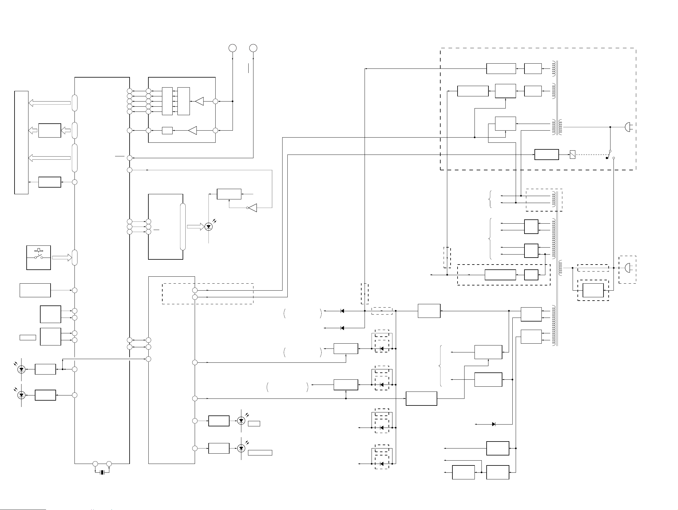
HCD-GRX9900/RXD9
7-4. BLOCK DIAGRAM – DISPLAY/KEY CONTROL/POWER SUPPLY Section –
D
FLUORESCENT INDICATOR TUBE DRIVER,
KEY CONTROL
IC601
BAND-PASS FILTER
IC603
SPEANA
(Page 23)(Page 23)
E
RESET
(RXD9)
+5V REGULATOR
IC11
SUB POWER TRANSFORMER
RECT
D12 – 15
T11
GRID DRIVE
Q611 – 616
FL601
FLUORESCENT INDICATOR TUBE
GRID DRIVE
Q610
S611 – 630,
S637 – 650, 801 – 807
REMOTE CONTROL
RECEIVER
IC602
LED DRIVE
Q607
LED DRIVE
Q608
D608, 609
ROTARY
ENCODER
S601
ROTARY
ENCODER
S602
S601
(JOG DIAL)
S602
VOLUME
D609
(RIGHT)
D608
(LEFT)
(FOR ILLUMINATION DISPLAY)
46 – 67
S1 – S22
32 – 27
G13 – G18
G2 – G12
44 – 42, 40 – 33
45
G1
11 – 14
KEY0 – KEY3
1
SIRCS
2
JOG-A
8
JOG-B
VOL-A
9
10
VOL-B
22
GRADATION R/WAKE UP
15
GRADATION L
05
S LOW FREQ (BPF0)
ALL BAND (L+R)
RESET
L SEL
LED DATA
LED SCK
LED LAT
I2C DATA
I2C CLK
XOUT
XIN
72
70
X601
12.5MHz
BPF1
BPF2
BPF3
BPF4
16
17
18
19
20
21
73
7
5
3
4
78
79
F01
17
F02
16
F04
14
DET
F05
13
F06
12
L+R
11
DET
LED DRIVER
IC604
DATA
13
14
CLK
15
STB
SYSTEM CONTROLLER
IC501 (4/4)
IIC-DATA
30
IIC-CLK
29
WAKE UP
18
LINE
B.P.F.
17, 19 – 23, 2, 3, 5, 7, 10, 11
P1 – P6, P8, P9, P11, P12, P15, P16
FL SW
STBY RELAY
CD-POWER
POWER
STBY LED
TIMER LED
IN
REC IN
42
43
5
2
39
26
LED DRIVE
Q604, 620
LED DRIVE
4
6
B+ SWITCH
Q601, 602
D611 – 615, 619,
D620, 622 – 626,
D631 – 634, 801 – 803
(RXD9)
Q605
LED +5V
Q603
D804
I/u
D636
TIMER SELECT
+5V
SYSTEM CONTROLLER
(IC501) B+
+5V (STBY)
(PANEL SECTION B+)
CD D+5V, CD A+5V
CD MECHANISM DECK
SECTION B+
D+5V
M62493FP (IC101),
CD SENSOR CIRCUIT B+
(RXD9)
D501, 502
D509
B+ SWITCH
Q907, 908
B+ SWITCH
Q904, 905
D+5V
(TAPE DECK SECTION B+)
LED +5V
(PANEL SECTION B+)
(GRX9900)
(RXD9)
D925
(GRX9900)
(RXD9)
D923
(GRX9900)
(RXD9)
D922
(GRX9900)
(RXD9)
D924
(GRX9900)
–26V
(FL DRIVER (IC601) B–)
REGULATOR
TC, PANEL,
REGULATOR
CONTROL SWITCH
Q903, 923
CD M+7V
(CD MOTOR SECTION B+)
TC M+12V
(TC MOTOR SECTION B+)
ST +10V
(FM/AM TUNER UNIT B+)
(RXD9)
+5V
IC902
AUDIO
–26V REGULATOR
POWER AMP (IC801),
PROTECTOR CIRCUIT
(GRX9900)
+7V
–7V
FAN MOTOR B–
+10V
REGULATOR
Q909
Q13
TO FLUORESCENT
INDICATOR TUBE
(FL601)
REGULATOR
Q901, 902, 913
REGULATOR
Q914, 951, 952
FL ON/OFF
SWITCH
Q12, 17
FL ON/OFF
SWITCH
Q14 – 16
VF1
VF2
B+
B–
B+
B–
–26V REGULATOR
Q971
+7V
–7V
D405 – 407
+7V
REGULATOR
IC901
+12V
REGULATOR
IC903
RECT
D17 – 20
(GRX9900)
RECT
D832
RECT
D831
RECT
D971
RECT
D901 – 904
RECT
D907 – 910
RELAY DRIVE
Q11
POWER TRANSFORMER
T951
RY11
(GRX9900: Mexican/RXD9)
VOLTAGE
SELECTOR
S951
(EXCEPT GRX9900: Mexican/RXD9)
AC IN
(GRX9900)
AC IN
– 25 –
– 26 –
7-5. NOTE FOR PRINTED WIRING BOARDS AND SCHEMATIC DIAGRAMS
CONNECTOR board
SENSOR board
MOTOR (TURN) board
MOTOR (SLIDE) board
LEAF SW board
AUDIO board
BD board
(In addition to this, the necessary note is printed in each block)
Note on Printed Wiring Board:
• X : parts extracted from the component side.
• Y : parts extracted from the conductor side.
• p : parts mounted on the conductor side.
¢
•
• b : Pattern from the side which enables seeing.
(The other layers' patterns are not indicated.)
Caution:
Pattern face side: Parts on the pattern face side seen from
(Side B) the pattern face are indicated.
Parts face side: Parts on the parts face side seen from
(Side A) the parts face are indicated.
• Indication of transisitor.
: internal component.
Q
B
CE
These are omitted.
Q
B
CE
These are omitted.
C
Q
B
E
These are omitted.
Note on Schematic Diagram:
• All capacitors are in µF unless otherwise noted. pF: µµF
50 WV or less are not indicated except for electrolytics
and tantalums.
• All resistors are in Ω and 1/
specified.
¢
•
• 2 : nonflammable resistor.
• 5 : fusible resistor.
• C : panel designation.
• U : B+ Line.
• V : B– Line.
• H : adjustment for repair.
• V oltages are taken with a VOM (Input impedance 10 MΩ).
• Waveforms are taken with a oscilloscope.
• Circled numbers refer to waveforms.
• Signal path.
• Abbreviation
: internal component.
Note: The components identified by mark ! or
dotted line with mark ! are critical for safety .
Replace only with part number specified.
Voltage variations may be noted due to normal production tolerances.
Voltage variations may be noted due to normal production tolerances.
F : TUNER (FM/AM)
E : PLAYBACK (DECK A)
d : PLAYBACK (DECK B)
G : RECORD
J : CD PLAY (ANALOG OUT)
c : CD PLAY (DIGITAL OUT)
N : MIC INPUT
AED : North European model
AR : Argentine model
E2 : 120 V AC Area in E model
E3 : 240 V AC Area in E model
EA : Saudi Arabia model
G : German model
MY : Malaysia model
MX : Mexican model
SP : Singapore model
4
W or less unless otherwise
• Circuit Boards Location
CD SW board
PANEL board
TRANS board
SUB TRANS board
(RXD9)
TUNER PACK
MAIN board
– 27 –
– 28 –
 Loading...