

Page 1
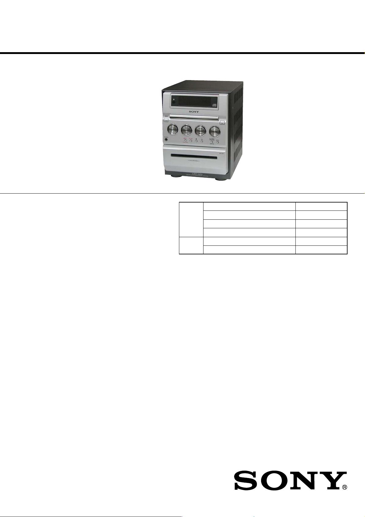
HCD-GP5
SERVICE MANUAL
Ver 1.5 2004.10
HCD-GP5 is the Amplifier, CD player, Tape
Deck and Tuner section in CMT-GP5.
CD
Section
TAPE
Section
US Model
Canadian Model
AEP Model
UK Model
E Model
Australian Model
Model Name Using Similar Mechanism NEW
CD Mechanism Type CDM55A-K6BD44B
Base Unit Name BU-K1BD44B
Optical Pick-up Name KSM-213D
Model Name Using Similar Mechanism NEW
Tape Transport Mechanism Type CMAL1Z240A
Amplifier section
AUDIO POWER SPECIFICATIONS:
(U.S.A. model only)
POWER OUTPUT AND TOTAL HARMONIC
DISTORTION:
With 6-ohm loads, both channels driven, from 120 10,000 Hz; rated 35 watts per channel minimum RMS
power, with no more than 10% total harmonic
distortion from 250 milliwatts to rated output.
North American model:
Continuous RMS power output (reference):
European model:
DIN power output (rated): 30 + 30 W
Continuous RMS power output (reference):
Music power output (reference ):
Other models:
The following measured at AC 230 V or AC 120 V, 50/
60 Hz
DIN power output (rated): 30 + 30 W
Continuous RMS power output (reference):
35 + 35 W
(6 ohms at 1 kH z, 10%
THD)
(6 ohms at 1 kH z, DIN)
30 + 30 W
(6 ohms at 1 kH z, 10%
THD)
60 + 60 W
(6 ohms at 1 kH z, DIN)
30 + 30 W
(6 ohms at 1 kH z, 10%
THD)
SPECIFICATIONS
Inputs
MD IN (phono jacks):
Outputs
PHONES (stereo minijack):
SPEAKERS: Accepts impedance of 6 to
CD player section
System Compact disc and digital
LaserSemiconductor laser
Frequency response 2 Hz – 20 kHz (±0.5 dB)
Tape deck section
Recording system 4-track 2-channel stereo
Frequency response 50 – 13,000 Hz (±3 dB),
Tuner section
FM stereo, FM/AM superheterodyne tuner
FM tuner section
Sensitivity 500 mV,
impedance 47 kilohms
Accepts headphones with
an impedance of 8 ohms or
more
16 ohms.
audio system
λ
=780 nm)
(
Emission duration:
continuous
using Sony TYPE I
cassettes
Tuning range 87.5 – 108.0 MHz (50-kHz
Antenna FM lead antenna
Antenna terminals 75 ohms balanced
Intermediate frequency 10.7 MHz
AM tuner section
Tuning range
Pan-American model: 530 – 1,710 kHz
European model: 531 – 1,602 kHz
Other models: 530 – 1,710 kHz
Antenna AM loop antenna, external
Intermediate frequency 450 kHz
step)
(with the tuning interval
set at 10 kHz)
531 – 1,710 kHz
(with the tuning interval
set at 9 kHz)
(with the tuning interval
set at 9 kHz)
(with the tuning interval
set at 10 kHz)
531 – 1,602 kHz
(with the tuning interval
set at 9 kHz)
antenna terminal
— Continued on next page —
9-877-380-06
2004J16-1
© 2004.10
MICRO HI-FI COMPONENT SYSTEM
Sony Corporation
Personal Audio Company
Published by Sony Engineering Corporation
Page 2

HCD-GP5
Ver 1.3 2004.01
TABLE OF CONTENTS
General
Power requirements
North American model: 120 V AC, 60 Hz
European model: 230 V AC, 50/60 Hz
Australian model: 230 - 240 V AC, 50/60 Hz
Hong Kong model:
Singaporean model:
Other models:
Power consumption
North American model: 60 watts
European model: 60 watts
Other models: 60 watts
Dimensions (w/h/d) Approx. 190 × 250 × 270
Mass Approx. 4.6 kg
Design and specifications are subject to change
without notice.
220 - 240 V AC, 50/60 Hz
220 - 240 V AC, 50/60 Hz
110 - 120 V or 220 - 240 V
AC, 50/60 Hz
Adjustable with voltage
selector
0.3 watts (in the standby
mode)
mm
1. SERVICING NOTES ······················································· 3
2. GENERAL ··········································································5
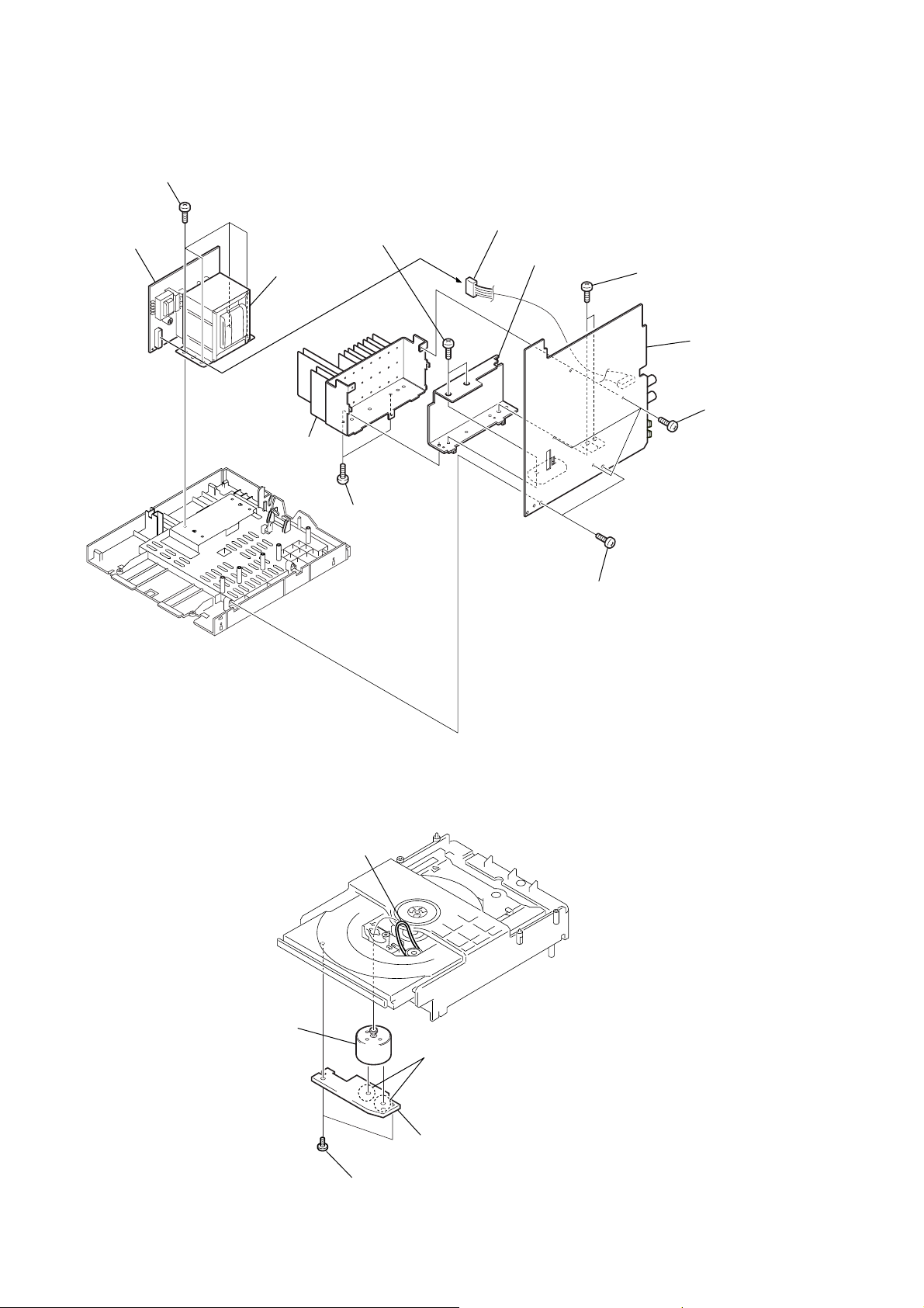
3. DISASSEMBLY
3-1. Top Cabinet, Rear Panel·················································· 7
3-2. Front Panel Assy ····························································· 8
3-3. CONTROL Board, Single Cassette Mechanism············· 8
3-4. CD Mechanism Deck (CDM55A-K6BD44B)················ 9
3-5. MAIN Board, TRANSFORMER Board······················· 10
3-6. LOADING Board·························································· 10
3-7. CD Board ······································································ 11
3-8. Tray (CDM55D) ··························································· 11
3-9. Optical Pick-up (KSM-213D), Holder (C213) ············· 12
4. MECHANICAL ADJUSTMENTS ····························· 13
5. ELECTRICAL ADJUSTMENTS ······························· 14
6. DIAGRAMS······································································ 17
6-1. Block Diagram ······························································ 19
6-2. Printed Wiring Board – CD Section – ························· 20
6-3. Schematic Diagram – CD Section – ···························· 21
6-4. Printed Wiring Board – Control Section – ··················· 22
6-5. Schematic Diagram – Control Section –······················ 23
6-6. Printed Wiring Boards – Main Section – ····················· 24
6-7. Schematic Diagram – Main Section (1/4) –················· 25
6-8. Schematic Diagram – Main Section (2/4) –················· 26
6-9. Schematic Diagram – Main Section (3/4) –················· 27
6-10. Schematic Diagram – Main Section (4/4) –··············· 28
6-11. Printed Wiring Board – Power Section – ··················· 29
6-12. Schematic Diagram – Power Section –······················ 30
6-13. IC Pin Function Description ······································· 35
SAFETY-RELATED COMPONENT WARNING!!
COMPONENTS IDENTIFIED BY MARK 0 OR DOTTED LINE WITH
MARK 0 ON THE SCHEMATIC DIAGRAMS AND IN THE PARTS
LIST ARE CRITICAL TO SAFE OPERATION. REPLACE THESE
COMPONENTS WITH SONY PARTS WHOSE PART NUMBERS
APPEAR AS SHOWN IN THIS MANUAL OR IN SUPPLEMENTS
PUBLISHED BY SONY.
ATTENTION AU COMPOSANT AYANT RAPPORT
À LA SÉCURITÉ!
LES COMPOSANTS IDENTIFÉS P AR UNE MARQUE 0 SUR LES
DIAGRAMMES SCHÉMA TIQUES ET LA LISTE DES PIÈCES SONT
CRITIQUES POUR LA SÉCURITÉ DE FONCTIONNEMENT. NE
REMPLACER CES COMPOSANTS QUE PAR DES PIÈSES SONY
DONT LES NUMÉROS SONT DONNÉS DANS CE MANUEL OU
DANS LES SUPPÉMENTS PUBLIÉS PAR SONY.
7. EXPLODED VIEWS
7-1. Overall Section ····························································· 37
7-2. Front Panel Section ······················································· 38
7-3. Chassis Section ····························································· 39
7-4. CD Mechanism Deck Setion········································· 40
7-5. KSM-213D···································································· 41
8. ELECTRICAL PARTS LIST ······································· 42
2
Page 3
SECTION 1
r
SERVICING NOTES
HCD-GP5
Notes on chip component replacement
•Never reuse a disconnected chip component.
• Notice that the minus side of a tantalum capacitor may be damaged by heat.
Flexible Circuit Board Repairing
•Keep the temperature of the soldering iron around 270 ˚C during
repairing.
• Do not touch the soldering iron on the same conductor of the
circuit board (within 3 times).
• Be careful not to apply force on the conductor when soldering or
unsoldering.
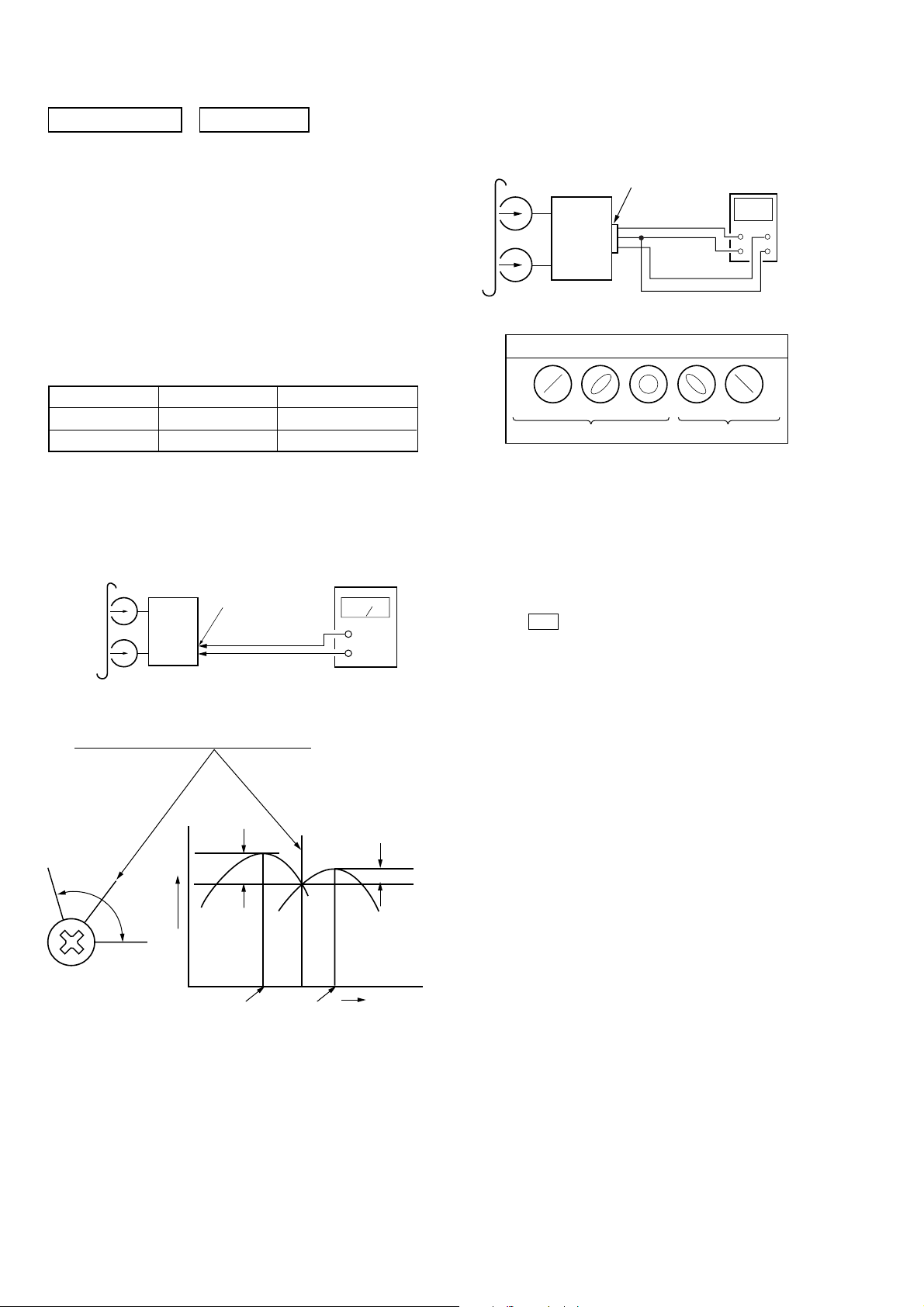
SAFETY CHECK-OUT
After correcting the original service problem, perform the following
safety check before releasing the set to the customer:
Check the antenna terminals, metal trim, “metallized” knobs, screws,
and all other exposed metal parts for AC leakage.
Check leakage as described below.
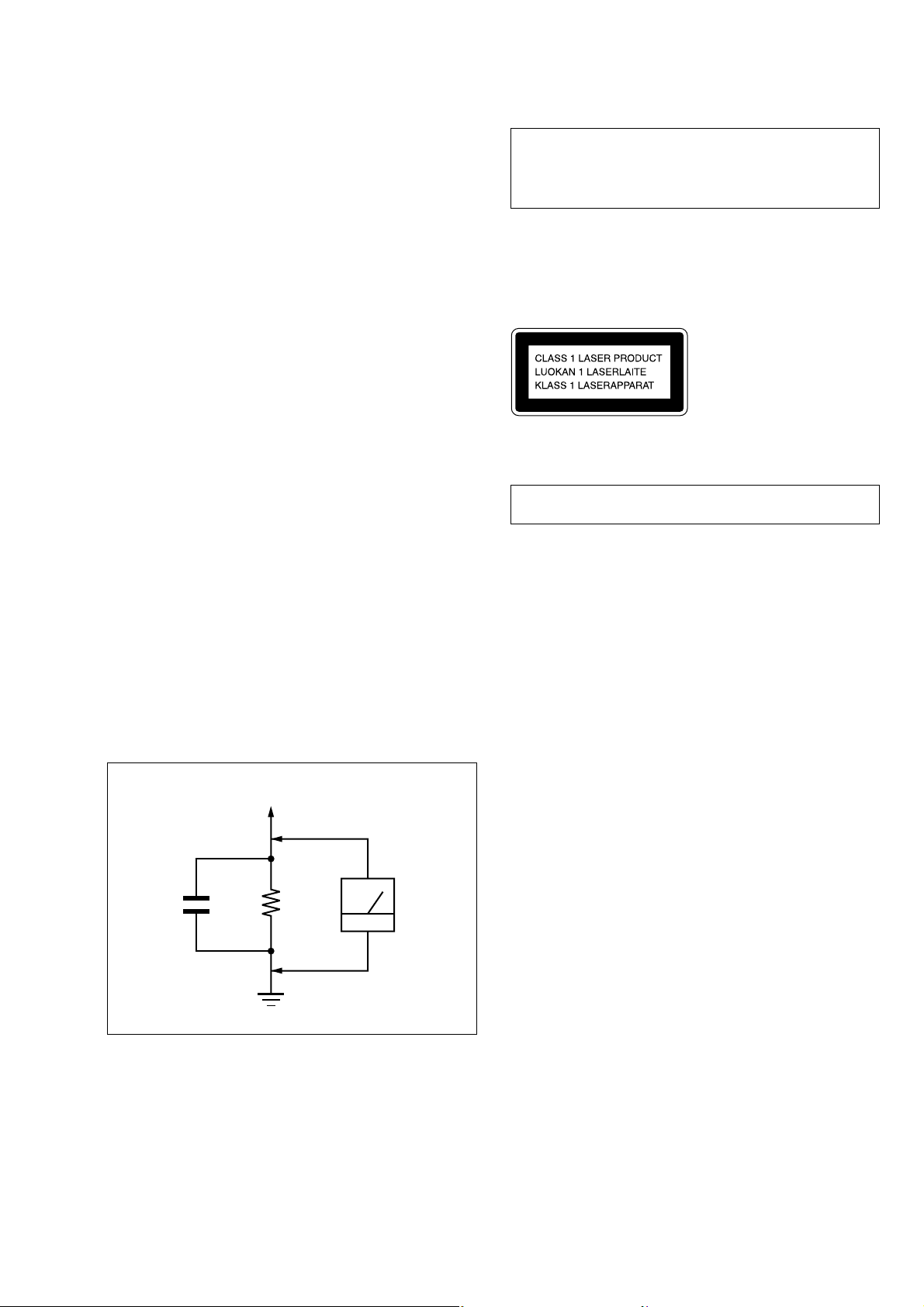
LEAKAGE TEST
The AC leakag e from any exposed metal part to earth ground and
from all exposed metal parts to any exposed metal part having a
return to chassis, must not exceed 0.5 mA (500 microamperes.).
Leakage current can be measured by any one of three methods.
1. A commercial leakage tester , such as the Simpson 229 or RCA
WT-540A. Follow the manufacturers’ instructions to use these
instruments.
2. A battery-operated AC milliammeter. The Data Precision 245
digital multimeter is suitable for this job.
3. Measuring the voltage drop across a resistor by means of a V OM
or battery-operated A C voltmeter . The “limit” indication is 0.75
V, so analog meters must have an accurate low-voltage scale.
The Simpson 250 and Sanwa SH-63Trd are examples of a
passive VOM tha t is suitable. Nearly all battery operated digital
multimeters that have a 2 V A C range are suitable. (See Fig. A)
To Exposed Metal
Parts on Set
CAUTION
Use of controls or adjustments or performance of procedures
other than those specified herein may result in hazardous
radiation exposure.
This appliance is classified as a CLASS 1 LASER product.
The CLASS 1 LASER PRODUCT MARKING is located on
the exterior.
Laser component in this product is capable of emitting radiation
exceeding the limit for Class 1.
NOTES ON HANDLING THE OPTICAL PICK-UP
BLOCK OR BASE UNIT
The laser diode in the optical pick-up block may suffer electrostatic
break-down because of the potential difference generated by the
charged electrostatic load, etc. on clothing and the human body.
During repair, pay attention to electrostatic break-down and also
use the procedure in the printed matter which is included in the
repair parts.
The flexible board is easily damaged and should be handled with
care.
NOTES ON LASER DIODE EMISSION CHECK
The laser beam on this model is concentrated so as to be focused on
the disc reflective surface by the objective lens in the optical pickup block. Therefore, when checking the laser diode emission,
observe from more than 30 cm away from the objective lens.
LASER DIODE AND FOCUS SEARCH OPERATION
CHECK
Carry out the “S curve check” in “CD section adjustment” and check
that the S curve waveforms is output three times.
1.5 k
0.15 µF
Fig. A. Using an AC voltmeter to check AC leakage.
Ω
Earth Ground
AC
voltmete
(0.75 V)
3
Page 4
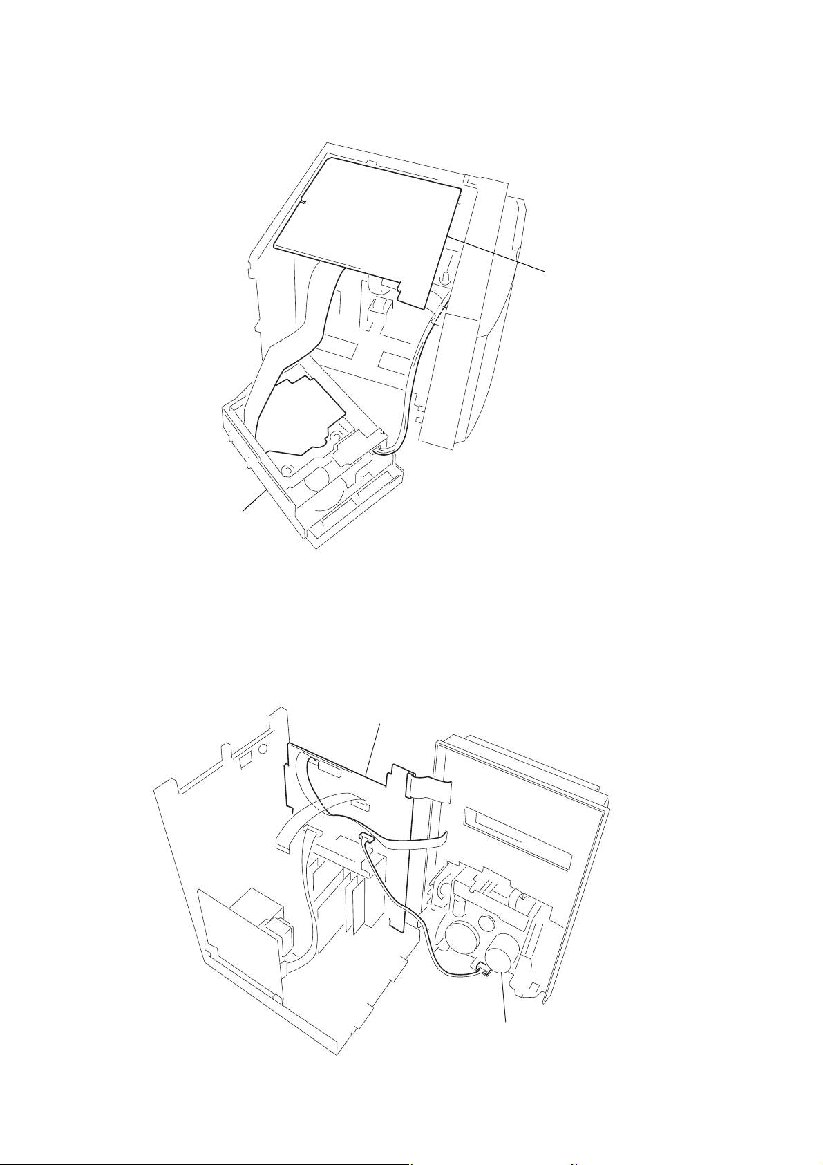
HCD-GP5
Service Position of the CD Mechanism Deck
MAIN Board
CD Mechanism Deck
(CDM55A-K6BD44B)
Service Position of the Tape Cassette Mechanism Deck
MAIN Board
Tape Cassette Mechanism Deck
(CMAL1Z240A)
4
Page 5
SECTION 2
Illustrati
GENERAL
List of button locations and reference pages
HCD-GP5
This section is extracted
from instruction manual.
How to use this page
Use this pa ge to fin d th e lo c atio n o f b u tto ns an d o th e r
parts of the system that are mentioned in the text.
Main unit
ALPHABETICAL ORDER
A – M
Cassette compartment qg
CD SYNC qd (12)
DIRECTION 9 (11, 12, 15)
Disc tray 4
DISPLAY 8 (9, 10, 16)
Display window 3
DSG qa (13)
MD qj (17)
P – Z
PHONES jack qh
PLAY MODE/TUNING MODE
9 (6, 7)
Remote sensor 2
TUNER/BAND qj (8, 9)
TUNING +/– 6 (8 , 9)
VOLUME +/– 7 (14, 15)
12 345
on number
r
DISPLAY 8 (9, 10, 16)
Name of button/par t Reference page
RR
BUTTON DESCRIPTIONS
?/1 (po w e r) 1 (5, 9, 14, 15)
.m/ M> (go back/go
forward or fast forward/
rewind) 6 (5, 6, 7, 11, 12, 14,
15, 16)
x (stop) qs (6, 7 , 11, 12, 20)
REC PAUSE/START z qf (12,
15)
CD NX (play/pause) qk (6 , 7)
TAPE nN (play) qk (11, 12,
15)
Z (CD open/close) 5 (6)
Z PUSH (tape open/close) 0
(11)
qk
qj
qh
6
7
8
9
qdqfqg
0qaqs
5
Page 6
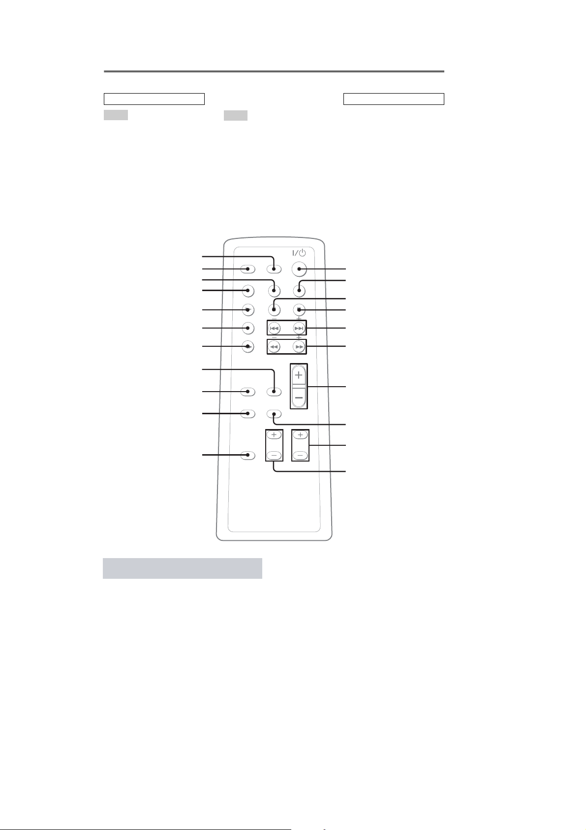
HCD-GP5
Remote control
ALPHABETICAL ORDER
A – M
BASS +/– 0 (13)
CLEAR 8 (8, 9)
CLOCK/TIMER SELECT w;
(14, 15)
CLOCK/TIMER SET wa (5, 14,
15)
DISPLAY 2 (9, 10, 16)
DSG qa (13)
MD qk (17)
wa
w;
ql
qk
qj
qh
qg
qf
P – Z
PLAY MODE/DIRECTION qd
(6, 7, 11, 12, 15)
PRESET +/– 5 (9)
REPEAT/FM MODE qf (7, 9)
SLEEP ql (13)
TREBLE +/– 9 (13)
TUNER BAND qh (8, 9)
TUNER MEMORY qs (8)
TUNING +/– 6 (8, 9)
VOL +/– 7 (14, 15)
BUTTON DESCRIPTIONS
?/1 (power) 1 (5, 9, 14, 15)
m/M (fast forward/re wind)
6 (6, 11)
./ > (go back/go forward)
5 (5, 6, 7, 12, 14, 15, 16)
x (s top) 4 (6, 7, 11, 12, 20)
X (pa us e) 3 (6, 11)
CD N (play) qj (6, 7)
TAPE nN (play) qg (11, 12,
15)
1
2
3
4
5
6
qd
qs
qa
Setting the clock
Use buttons on the remote for the operation.
Press ?/1 to turn on the system.
1
Press CLOCK/TIMER SET.
2
Press ./> repeatedly to set the
3
hour.
Press CLOCK/TIMER SET.
4
Press ./> repeatedly to set the
5
minute.
Press CLOCK/TIMER SET.
6
The clock starts working.
To adjust the clock
Press CLOCK/TIMER SET.
1
Press ./> to select “CLOCK”, then
2
press CLOCK/TIMER SET.
Do the same procedures as step 3 to 6
3
above.
7
8
9
0
6
Page 7
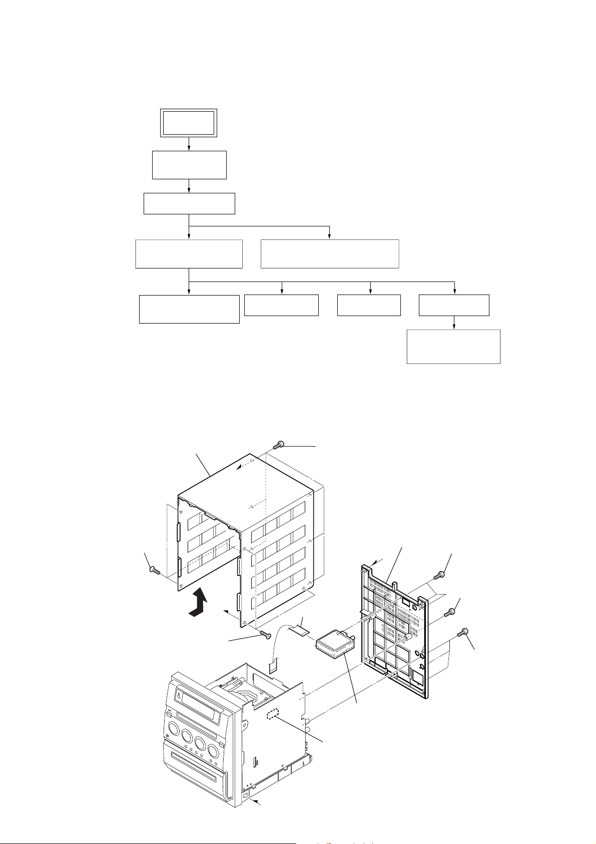
• This set can be disassembled in the order shown below.
SET
TOP CABINET,
REAR PANEL
FRONT PANEL ASSY
SECTION 3
DISASSEMBLY
HCD-GP5
Ver 1.2 2003.11
CD MECHANISM DECK
(CDM55A-K6BD44B)
MAIN BOARD,
TRANSFORMER BOARD
Note: Follow the disassembly procedure in the numerical order given.
CONTROL BOARD,
SINGLE CASSETTE MECHANISM
LOADING BOARD CD BOARD TRAY (CDM55D)
3-1. Top Cabinet, Rear Panel
5
2
three s
(+KTP 3
crews
×
12)
top cabinet
a
3
six s
crews
(+BVTP 3
OPTICAL PICK-UP
(KSM-213D),
HOLDER (C213)
×
10)
qa
rear panel
a
9
three s
(+BVTP 3
crews
×
10)
4
1
three s
(+KTP 3
crews
×
12)
7
two s
crews
b
b
6
w
ire (flat type)
11p
CN304
q;
tuner (FM/AM)
(+BVTP 3
8
(+BVTP 3
three s
×
10)
crews
×
10)
7
Page 8
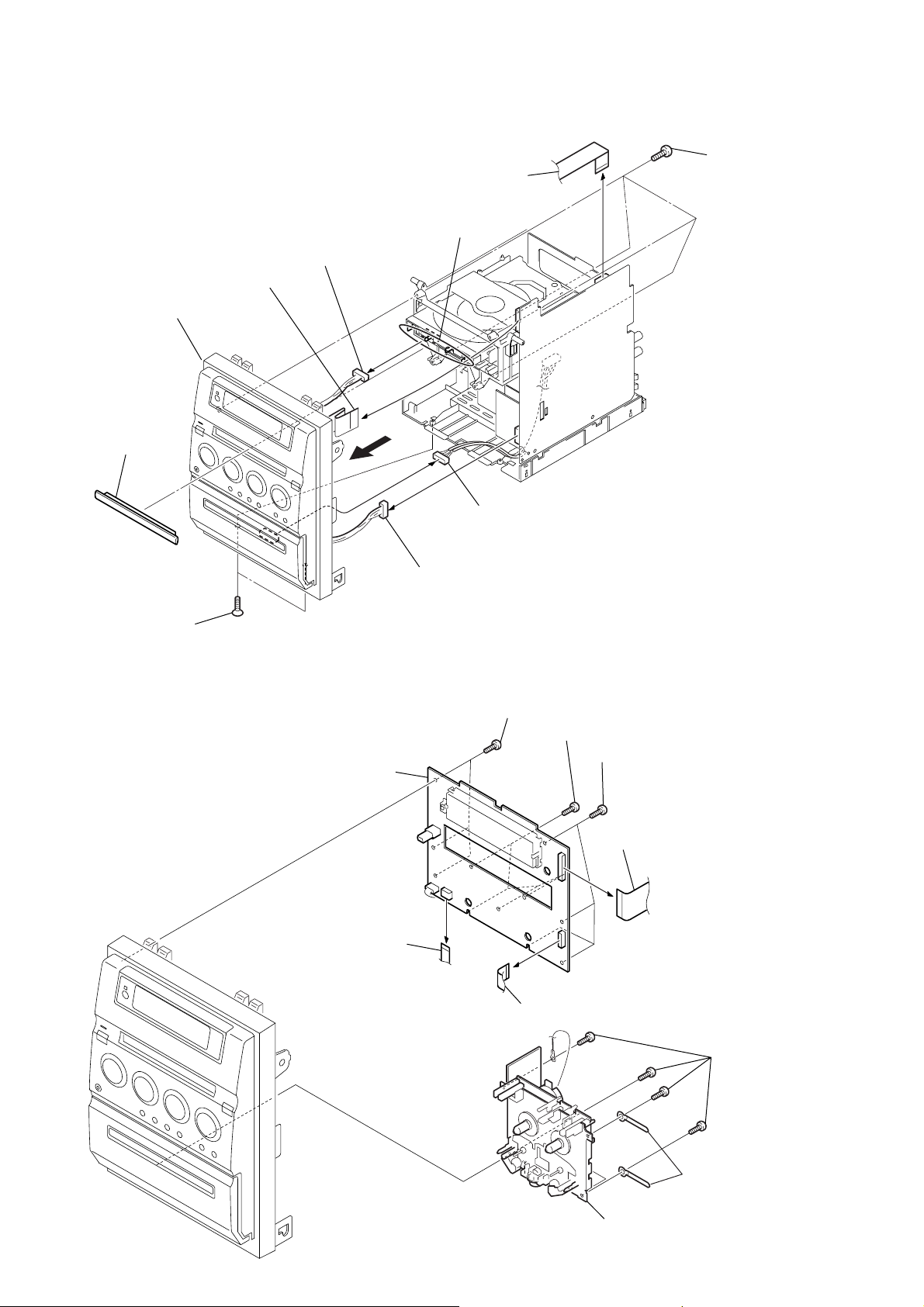
HCD-GP5
3-2. Front Panel Assy
6
w
ire (flat type) 26p (CN302)
q;
front panel assy
2
CD lid
7
connector 5p (CN1)
5
w
ire (flat type) 13p (CN303)
1
four claws
4
four s
(+BVTP 3
crews
×
10)
3
two s
(+KTP 3
crews
×
12)
3-3. CONTROL Board, Single Cassette Mechanism
7
CONTROL
6
w
ire (flat type) 8p (CN603)
board
8
connector 6p
9
connector 5p (CN201)
1
three s
crews (+BVTP 3
2
four s
crews (+BVTP 3
3
four s
4
×
10)
×
10)
crews (+BVTP 3
w
ire (flat type) 26p (CN601)
×
10)
5
w
ire (flat type) 13p (CN602)
8
four s
crews
×
10)
9
two clamp
q;
single cassette mechanism
(CMAL1Z240A)
(+BVTP 3
8
Page 9
3-4. CD Mechanism Deck (CDM55A-K6BD44B)
)
1
CD plate
7
CD mechanism deck
(CDM55A-K6BD44B)
5
6
CD holder
4
s
crew (+BVTP 3
CN101
×
10)
3
w
ire (flat type) 21p (CN101,305
HCD-GP5
CN305
2
s
crew (+BVTP 3
×
10)
9
Page 10
HCD-GP5
)
3-5. MAIN Board, TRANSFORMER Board
q;
four s
(+BVTP 3
qs
TRANSFORMER
board
crews
×
10)
6
two s
(+BVTP 3
qa
power transformer
5
main heat sink
crews
1
×
10)
connector 9p (CN801)
8
sub heat sink
7
two s
crews
(+BVTP 3
9
×
10)
MAIN board
3
three s
(+BVTP 3
crews
×
10
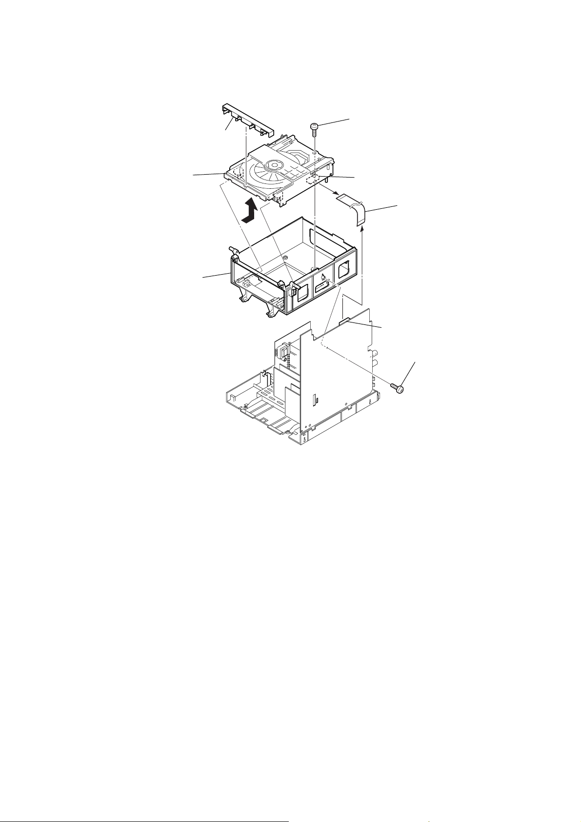
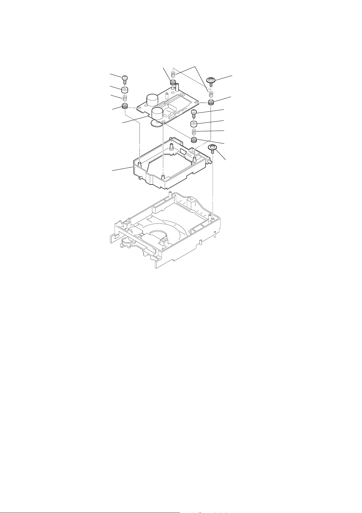
3-6. LOADING Board
1
Remove the belt.
4
two s
(+BVTP 3
crews
×
10)
2
two s
crews (+BVTP 3
×
10)
10
4
motor
(M901)
(LD) assy
2
two
screws (+BTP 2.6
3
Remove soldering from the two points.
5
LOADING board
×
6)
Page 11
p
3-7. CD Board
4
wire (flat type) 21p (CN101)
2
Remove soldering
from the four points.
1
screw(+P 2.6
5
CD board
×
5)
3
wire (flat type) 16
HCD-GP5
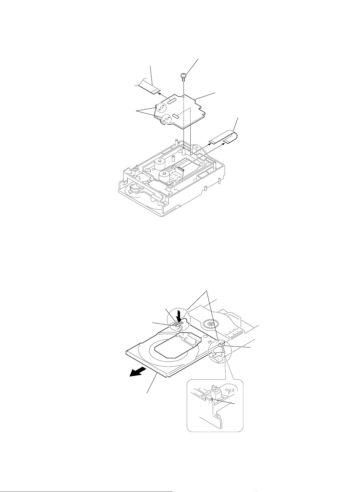
3-8. Tray (CDM55D)
1
While pressing the two protrusions A and B to unlock the two claws as shown,
pull the tray in the direction of the arrow C. (Be careful of the claws.)
A
claw
claw
C
2
tray
B
11
Page 12
HCD-GP5
s
Ver 1.2 2003.11
3-9. Optical Pick-up (KSM-213D), Holder (C213)
3
5
screw (+PTTP M2.6)
6
stopper (BU)
7
compression spring
(T213)
8
insulator
qd
optical pick-up
(KSM-213D)
qg
holder
(C213)
insulator
2
two compression spring
1
(+PTPWH M2.6)
4
9
screw (+PTTP M2.6)
q;
stopper (BU)
qa
compression spring
(T213)
qs
insulator
qf
floating
(+PTPWH M2.6)
(T213)
two floating
insulator
screws
screw
12
Page 13
SECTION 4
MECHANICAL ADJUSTMENTS
Precaution
1. Clean the following parts with a denatured alcohol-moistened
swab:
record/playback heads pinch rollers
erase head rubber belts
capstan idlers
2. Demagnetize the record/playback head with a head demagnetizer.
3. Do not use a magnetized screwdriver for the adjustments.
4. After the adjustments, apply suitable locking compound to the
parts adjusted.
5. The adjustments should be performed with the rated power
supply voltage unless otherwise noted.
Torque Measurement
HCD-GP5
Mode
FWD
FWD
back tension
REV
REV
back tension
FF/REW
FWD tension
REV tension
Torque meter Meter reading
3.04 – 6.96 mN • m
CQ-102C
CQ-102C
CQ-102RC
CQ-102RC
CQ-201B
CQ-403A
CQ-403R
(31 to 71 g • cm)
(0.43 – 0.98 oz • inch)
0.20 – 0.58 mN • m
(2 to 6 g • cm)
(0.02 – 0.08 oz • inch)
3.04 – 6.96 mN • m
(31 to 71 g • cm)
(0.43 – 0.98 oz • inch)
0.20 – 0.58 mN • m
(2 to 6 g • cm)
(0.02 – 0.08 oz • inch)
6.97 – 14.02 mN • m
(71 to 143 g • cm)
(0.98 – 1.99 oz • inch)
9.8 mN • m or more
(100 g • cm or more)
(1.4 oz • inch or more)
9.8 mN • m or more
(100 g • cm or more)
(1.4 oz • inch or more)
13
Page 14
HCD-GP5
SECTION 5
ELECTRICAL ADJUSTMENTS
DECK SECTION 0 dB=0.775V
1. Demagnetize the record/playback head with a head demagnetizer.
2. Do not use a magnetized screwdriver for the adjustments.
3. After the adjustments, apply suitable locking compound to the
parts adjusted.
4. The adjustments should be performed with the rated power
supply voltage unless otherwise noted.
5. The adjustments should be performed in the order given in this
service manual. (As a general rule, playback circuit adjustment
should be completed before performing recording circuit
adjustment.)
6. The adjustments should be performed for both L-CH and RCH.
7. Switches and controls should be set as follows unless otherwise
specified.
Signal Used forTape
P-4-A100
WS-48B
[Record/Playback Head Azimuth Adjustment]
Procedure:
1. Mode : Playback
test tape
P-4-A100
(10kHz, –10dB)
2. Turn the adjustment screw and check output peaks. If the peaks
do not match for L-CH and R-CH, turn the adjustment screw
so that outputs match within 1 dB of peak.
10 kHz, –10 dB
3 kHz, 0 dB
MAIN board
J203
speaker terminal
set
Azimuth Adjustment
Tape Speed Adjustment
level meter
+
–
3. Mode: Playback
test tape
P-4-A100
(10kHz, –10dB)
set
in phase 45
MAIN board
J203
speaker terminal
L
R
Waveform of oscilloscope
°
90
°
good
135
oscilloscope
°
wrong
180
°
4. After the adjustments, apply suitable locking compound to the
parts adjusted.
Adjustment Location:Record/Playback/Erase Head
[Tape Speed Check]
Procedure:
1. Turn the power on.
2. Insert the WS-48B into deck.
3. Press the Y button of deck.
4. Check the reading of frequency counter becomes 3000 ± 90 Hz.
Sample Value of Wow and flutter
W.RMS (JIS) less than 0.3%
(test tape: WS-48B)
L-CH
peak
screw
position
14
R-CH
peak
output
level
within
1 dB
L-CH
peak
R-CH
peak
within 1dB
screw
position
Page 15
HCD-GP5
+
–
CD board
TP (RFAC)
TP (VC)
oscilloscope
CD SECTION
Note:
1. CD Block is basically designed to operate without adjustment. Therefore, check each item in order given.
2. Use YEDS-18 disc (3-702-101-01) unless otherwise indicated.
3. Use an oscilloscope with more than 10MΩ impedance.
4. Clean the object lens by an applicator with neutral detergent when the
signal level is low than specified value with the following checks.
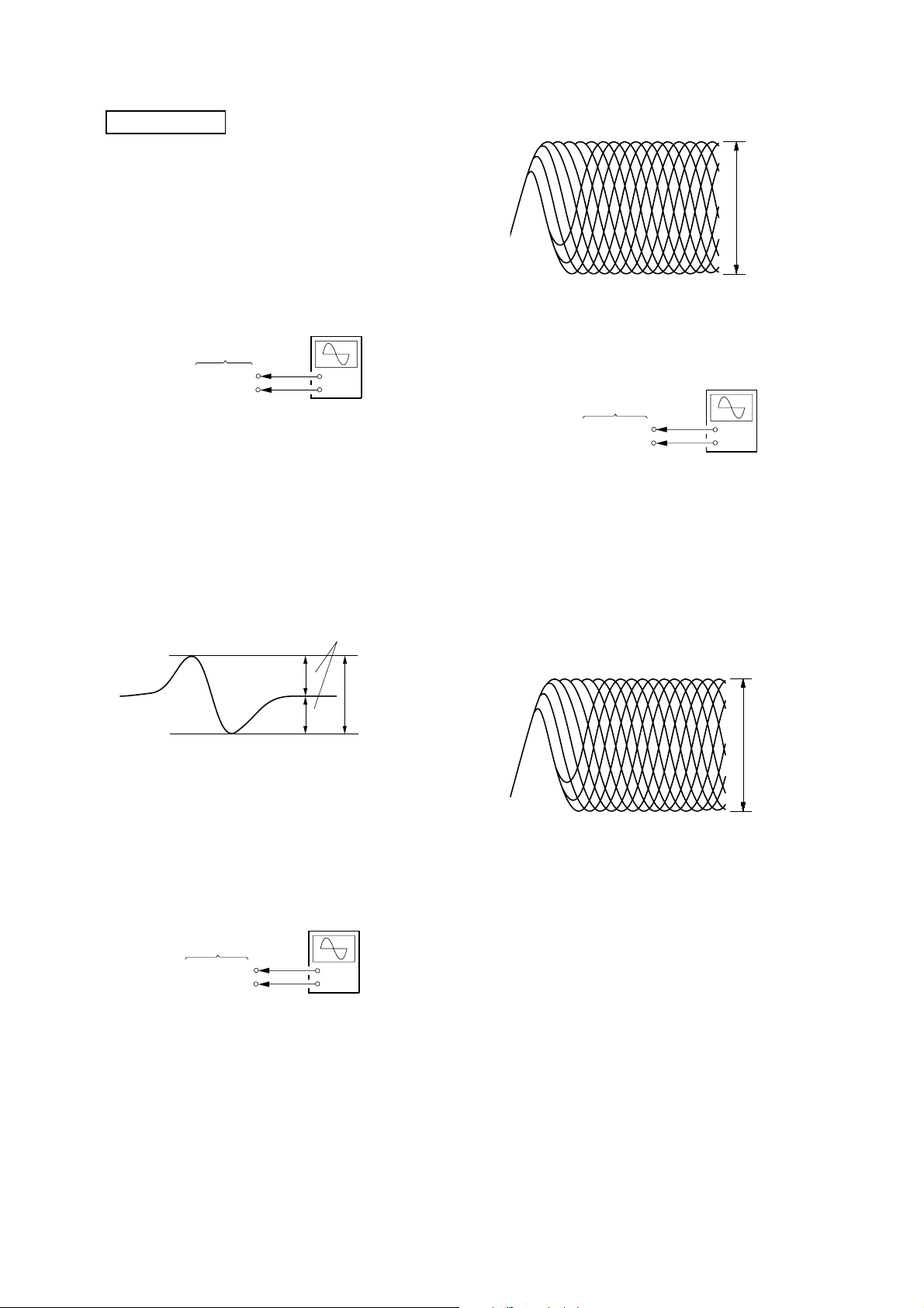
S-curve Check
Connection:
oscilloscope
CD board
TP (FE)
TP (DVC)
Procedure:
1. Connect an oscilloscope to test point TP (FE) and TP (DVC)
on the CD board.
2. Turn the power on.
3. Put the disc (YEDS-18) in and turned power switch on again
and actuate the focus search. (actuate the focus search when
disc table is moving in and out)
4. Check the oscilloscope waveform (S-curve) is symmetrical
between A and B. And confirm peak to peak level within 2 ± 1
Vp-p.
S-curve waveform
+
–
symmetry
A
B
within 2
±
1 Vp-p
RFDC signal waveform
VOLT/DIV: 200 mV
TIME/DIV: 500 ns
level: 0.7
±
0.2 Vp-p
Checking Location: CD board (Conductor side)
RFAC Level Check
Connection:
Procedure:
1. Connect an oscilloscope to test point TP (RFA C) and TP (VC)
on the CD board.
2. Turn the power on.
3. Put the disc (YEDS-18) in to playback the number five track.
4. Confirm that oscilloscope waveform is clear and check RF AC
signal level is correct or not.
Note: A clear RFAC signal waveform means that the shape “◊” can be
clearly distinguished at the center of the waveform.
RFAC signal waveform
VOLT/DIV: 200 mV
TIME/DIV: 500 ns
Note: •Try to measure several times to make sure than the ratio of A : B
or B : A is more than 10 : 7.
•Take sweep time as long as possible and light up the
brightness to obtain best waveform.
Checking Location: CD board (Conductor side)
RFDC Level Check
Connection:
oscilloscope
CD board
TP (RFDC)
TP (DVC)
+
–
Procedure:
1. Connect an oscilloscope to test point TP (RFDC) and TP (DVC)
on the CD board.
2. Turn the power on.
3. Put the disc (YEDS-18) in to playback the number five track.
4. Confirm that oscilloscope waveform is clear and check RFDC
signal level is correct or not.
Note: A clear RFDC signal waveform means that the shape “◊” can be
clearly distinguished at the center of the waveform.
level: 0.9
Checking Location: CD board (Conductor side)
±
0.4 Vp-p
15
Page 16
HCD-GP5
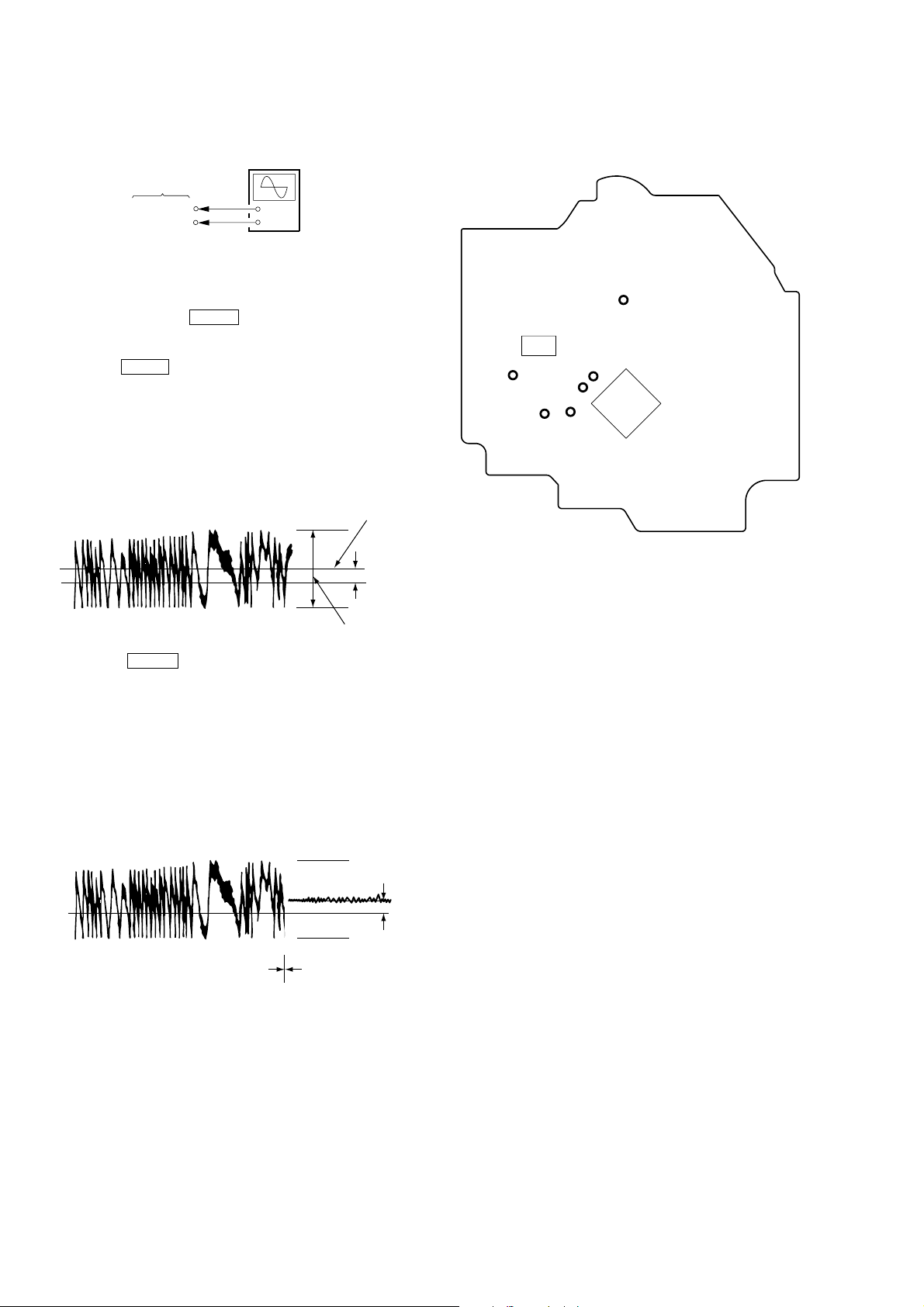
E-F Balance Check
Connection:
oscilloscope
CD board
TP (TE)
TP (DVC)
+
–
Procedure:
1. Connect an oscilloscpe to test point TP (TE) and TP (DVC) on
the CD board.
2. AC is put in pushing CD u button.
3. FL tube carries out all lights and goes into CD test mode.
4. Put the disc (YEDS-18) in to playback the number five track.
5. Press the CD u button. (The tracking servo and the sledding
servo are turned OFF)
6. Check the level B of the oscilliscope's waveform and the A
(DC voltage) of the center of the Traverse waveform.
Confirm the following :
A/B x 100 = less than ± 22%
Tr averse Waveform
0V
Center of
the waveform
B
A (DC
voltage)
Checking Location:
– CD BOARD (Conductor Side) –
TP (VC)
IC103
TP
(RFAC)
TP (TE)
TP (FE)
TP
(DVC)
IC101
TP
(RFDC)
level: 1.15 ± 0.5 Vp-p
7. Press the CD u button. (The tracking servo and sledding
servo are turned ON)
Confirm the C (DC voltage) is almost equal to the A (DC
voltage) is step 4.
8. To exit from this mode, turn the power off.
Notes: •Always move the optical pick-up to most inside track when
0V
exiting from this mode. Otherwise, a disc will not be unloaded.
• Do not run the sled motor excessively, otherwise the gear can
be chipped.
Tr averse Waveform
Tr acking servo
Sled servo
OFF
Tr acking servo
Sled servo
ON
C (DC
voltage)
Checking Location: CD board (Conductor side)
16
Page 17

• Circuit Boards Location
B
These are omitted.
CE
TRANSFORMER board
CONTROL board
HEADPHONE board
LOADING board
SECTION 6
DIAGRAMS
HCD-GP5
Ver 1.3 2004.01
CD board
MAIN board
THIS NOTE IS COMMON FOR PRINTED WIRING BOARDS AND SCHEMATIC DIAGRAMS.
(In addition to this, the necessary note is printed in each block.)
For schematic diagrams.
Note:
• All capacitors are in µF unless otherwise noted. pF: µµF
50 WV or less are not indicated except for electrolytics
and tantalums.
• All resistors are in Ω and 1/
specified.
f
•
• 2 : nonflammable resistor.
• 1 : fusible resistor.
• C : panel designation.
• A : B+ Line.
• B : B– Line.
•Voltages are taken with a VOM (Input impedance 10 MΩ).
•Waveforms are taken with a oscilloscope.
• Circled numbers refer to waveforms.
• Signal path.
•Abbreviation
: internal component.
Note:
The components identified by
mark 0 or dotted line with mark
0 are critical for safety.
Replace only with part number
specified.
Voltage variations may be noted due to normal production tolerances.
Voltage variations may be noted due to normal production tolerances.
F : TUNER
J : CD
d : MD
E : PB (TAPE)
a : REC (TAPE)
AUS: Australian model
CND : Canadian model
E51 : Chilean and Peruvian models
HK : Hong Kong model
KR : Korean model
SP : Singapore model
TW : Taiwan model
4
W or less unless otherwise
Note:
Les composants identifiés par
une marque 0 sont critiques
pour la sécurité.
Ne les remplacer que par une
pièce portant le numéro spécifié.
For printed wiring boards.
Note:
• X : parts extracted from the component side.
• Y : parts extracted from the conductor side.
f
•
• : Pattern from the side which enables seeing.
: internal component.
• Indication of transistor
C
Q
B
E
B
These are omitted.
CE
These are omitted.
17
Page 18

HCD-GP5
7
Q301 collector (Rec mode)
5V/DIV, 5
µs
/DIV
10.6Vp-p
10.9
µ
s
•Waveforms
– CD Board –
1 IC103 qg (RFAC)
(CD Play Mode)
– CONTROL Board – – MAIN Board –
5
IC601 qd (O-XT2)
200mV/DIV,
1 µs
2 IC101 el (FE)
(CD Play Mode)
50mV/DIV,
200 µs
3 IC101 ra (TE)
(CD Play Mode)
100mV/DIV,
200 µs
4 IC101 yj (XTAO)
59ns
1V/DIV,
20ns
/DIV
1.1Vp-p
/DIV
200mVp-p
/DIV
250mVp-p
/DIV
5.4Vp-p
30.5
µ
s
2V/DIV,
6
IC601 qh (XOUT)
116ns
1V/DIV,
10 µs
40ns
5.4Vp-p
/DIV
2.7Vp-p
/DIV
18
Page 19

6-1. Block Diagram
OPTICAL PICK-UP
BLOCK
(KSM-213D)
VC
+5V
A
B
C
D
E
F
Q101
LD
DRIVE
F-
T-
SLED
M
MOTOR
SPINDLE
M
MOTOR
VR
FOCUS
COIL
TRACKING
COIL
LD
GND
PD
F+
T+
RF AMP
IC103
VC
27
RFDCO
A
6
B
7
C
8
D
9
E
10
F
11
LD
1
PD
2
MOTOR/COIL DRIVE
IC102
CH1RO
13
CH1FO
14
CH2RO
11
CH2FO
12
CH3RO
18
CH3FO
17
CH4RO
16
CH4FO
15
MD
RFAC
FE
TE
FEI
SW
CH1RI
CH1FI
CH2RI
CH2FI
CH3RI
CH3FI
CH4INS
MUTE
J201
L
R
TUNER UNIT
STEREO
RDS SIG
RDS DATA
RDS CLK
15
28
16
18
17
29RFDCI
12
3
2
6
5
23
24
25
20
DECK BLOCK
REC/PB
HEAD
ERASE
HEAD
DECK BLOCK
SW1
PLAY
SW2
R REC
SW3
F REC
SW4
PACK
SW5
END
M1
DECK
MOTOR
+10V
L-CH
R-CH
D OUT
D IN
CLK
TUNED
MUTE
M
HCD-GP5
Ver 1.2 2003.11
PB/REC EQ AMP
IC301
OUT L
AUX L
19 18
R-CH
Q314-316
REG
+VM
+5V
R-CH
CE
DIGITAL SERVO
IC101
L OUT
RFAC
R-CH
R-CH
Q607
51
43
39
41
40
32
33
30
31
29
28
26
L301
BIAS
RFDC
FE
TE
SE
FFDR
FRDR
TFDR
TRDR
SRDR
SFDR
MDP
Q606
MOTOR
DRIVE
Q605
T SOL
DRIVE
R OUT
DATA
CLOK
XLAT
SQCK
SCLK
SCOR
SQSO
SENS
XTAI
XTAO
SSTP
XRST
BIAS
OSC
Q301
Q302
Q303,304
72
75
5
7
6
2
9
20
1
8
66
67
27
3
Q305-311
REC/PB
SWITCH
+VM
R-CH
X101
16.9344MHz
S101
LIMIT
23
21
2
+3.3V +5.5V
TU L
CD L
TAPE L
Q102,D101
+3.3V
REG
OUT R
CONT
REC OUT
R-CH
16
13
28
X601
32.768kHz
X602
8.64MHz
10
F DATA
83
O PW M3E
99
R COUNT
98
R DATA
100
R CLK
84
R CE
93
R TUNED
92
R STEREO
80
R MUTE
23
RDS SIG
91
RDS DATA
27
RDS CLK
87
C DATA
97
C CLK
86
C XLT
96
C SQSD
88
C SQCK
3
C SCOR
94
C SENS
85
C XRST
1
C PWM1
2
C PWM2
95
C LDON
12
13
15
16
7
77
T REC
81
O BIAS
79
T PLAY SW
24
T SW
5
T END
6
T MTR CONT
4
T SOL
I XT1
O XT2
X IN
X OUT
O SHIFT
µ CON
IC601
P AMP MUTE
P MONI
SEG20
GRID1
GRID11
I KEY2
LED CONT
CD DOOR SW
O CLOSE
RMC IN
I RESET
POWER DOWN
CD ON
POWER CONT
SEG1
76O DSG
9
8P CONT
25
45
.
47
50
.
52
66
34
44
18I KEY1
19
75
28
74O OPEN
73
29
Q601
RESET
11
SWITCH
26
82
8
MUTE
FL601
FLUORESCENT
DISPLAY
STANDBY
5
4
2
IC603
REMOTE
CONTROL
RECEIVER
Q504
Q503
PWR
CONT
HOLD
Q507
MOTOR DRIVE
IC604
VM
FIN
RIN
31
IC602
RESET
Q312
MUTE CONT
Q506
FIL1 FIL2
S601-607,612
FUCTION
KEY
S608-611
S613-616
FUCTION
KEY
LED601
ECO LED
+VM (7V)
OUT1
OUT2
µCON +B
POWER AMP
IC201
12
L IN
10
STBY
Q508
AC
DET
D502
7
9
D603
D608
21
D609
4L OUT
3R OUT
+PRE
5
+VCC
2
-VCC
1
Q509,510
DC
DET
+VM
CD DOOR
MOTOR UNIT
OPEN
CLOSE
TRAY
M
MOTOR
Q602-604
+5V
REG
+VH
Q501,502
OVER LOAD
DET
D434 D435
D605
J202
PHONES
• RCH is omitted due to same as L-CH.
• Signal Path
L
J203
SPEAKER
R
D402
D403
D410
D407
D405
D406
D404
V ECO
J204
SUBWOOFER
D416
FIL1
FIL2
D801-804
PT801
POWER
TRANS
PT802
SUB TRANS
+7V
Q410
DC
DET
+VL
Q411
DC
DET
-VL
Q419
+5V
REG
D422
D425
D423
D427
Q408,409
+VH
REG
Q404
-VH
REG
Q413
-VFL
REG
Q407
+VCC
REG
D436
CD P CONT
Q415,417,418
Q401 RY801
RELAY
DRIVE
D417
D413
D409
Q402,403,405
+VM
REG
Q416
+7V
REG
D418
D431
D432
+VH
-VH
+VP
+VL
-VP
-VL
-VFL
+VM
+VCC
P CONT
VM
Q406
+7V
CD +5V
: TUNER
: CD
: MD
: PB (TAPE)
: REC (TAPE)
L801
LINE
FILTER
AC
IN
1919
Page 20

HCD-GP5
Ver 1.2 2003.11
6-2. Printed Wiring Board – CD Section –
A
B
• See page 17 for Circuit Boards Location.
D
• Semiconductor
Location
Ref. No. Location
D101 F-5
IC101 E-4
IC102 C-5
IC103 D-2
Q101 C-2
Q102 G-5
TP (VC)
C
D
E
IC102
IC103
TP (RFAC)
TP (DVC)
IC101
CN305
24
F
G
12
1-680-849-
345678
2020
Page 21

6-3. Schematic Diagram – CD Section –
HCD-GP5
Ver 1.2 2003.11
• See page 18 for Waveforms. • See page 31, 32 for IC Block Diagrams.
KSM-213D
(1/4)
CN305
0uH
0uH
25
2121
Page 22

HCD-GP5
Ver 1.3 2004.01
6-4. Printed Wiring Board – Control Section –
CONTROL BOARD
C
TO
MAIN
BOARD
CN302
(Page 24)
• See page 17 for Circuit Boards Location.
E51,HK,SP,
TW,AUS
US,CND,AEP,UK,KR
IC601
FLUORESCENT INDICATOR TUBE
3
IC602
• Semiconductor
Location
Ref. No. Location
D601 A-2
D602 B-5
D603 B-6
D604 B-5
D605 A-1
D606 D-5
D607 B-5
D608 B-5
D609 B-5
IC603
IC601 A-3
IC602 B-5
IC603 B-6
124
IC604 D-7
Q601 B-4
Q602 A-2
Q603 A-2
Q604 A-2
Q605 D-5
Q606 D-5
Q607 E-6
Q608 B-6
B
TO
MAIN
BOARD
CN303
(Page 24)
STANDBY
Z
?/1
VOL
+
+
M >
CD
NX
TUNER/
BAND
IC604
. m
–
VOL
TAPE
bB
–
MD
TAPE
MECHANISM
DECK
DISPLAY
PLAY MODE/
TUNING MODE
DSG
x
CD SYNC
zREC
PAUSE/START
1-689-573-
LOADING BOARD
12
(12)
M901
2222
1-674-336-
Page 23

6-5. Schematic Diagram – Control Section –
HCD-GP5
Ver 1.3 2004.01
• See page 18 for Waveforms. • See page 33 for IC Block Diagram. • See page 35 for IC Pin Function Description.
TO
MAIN
BOARD
(1/4)
CN302
(Page 25)
SLR-342VCT31
STANDBY
2SA1981Y
SWITCH
IC603
5.3
270
0
TUNER/BAND
RPM7140-V4
5.3
0
5.3
x
MD
Y
TAP E
CD
u
-
REC
. m
z
PAU SE /START
+
M >
CN602
13P
Z
TO
MAIN
BOARD
B
(1/4)
CN303
(Page 25)
CONTROL BOARD
FLUORESCENT INDICATOR TUBE
Q602-Q604
5V REGULATOR
5.9
9.5
2.5
1.9
2SA1296
GR-(TYPE2)
10.2
(0.9)
10.2
(10.2)
8.8
8.2
1SS133T-77
10.2
(10.2)
1SS133T-72
2.5
9.5
(10.2)
0.5
1N4148A
-T265
1N4148A-T265
10.1
(1.0)
Q605
T SOL DRIVE
Q606
MOTOR DRIVE
1SS133
T-72
1SS133T-72
5.6
5.6
IC602
RESET
Q601
RESET
2SC2712L
-TE85R
0
MOTOR DRIVE
OTHER MODELS
3.9K
22K
22K
NO MOUNT
22K
4.7
0
0
10.2
10.2
4.0
270
LOADING
BOARD
CN151
5P
I/1
S1
(OPEN/CLOSE)
M901
(TRAY)
+
US, CND, AEP, UK, KR
NO MOUNT
33P
10K
10K
0
1K
R601
R631
R700
R701
R702
IC601
u Com
LC876764C-51E5
6
5
5.1
1SS133T-72
IC604
T-72
100K
C
CN601
26P
IC601
VOLTAGE CHART
PIN NO. PIN NO. PIN NO.
VOLT. VOLT. VOLT.
12.3 41-31.0 81 0.5
22.3 42-31.0 82 5.2
3043-31.0 83 0.4
40.8 44-31.0 84 0
55.3 45-31.0 85 5.2
6 10.2 46 5.2 86 5.2
7047-31.0 87 5.2
85.1 48-31.0 88 5.2
9049-31.0 89 0
10 0 50 -31.0 90 5.2
11 5.1 51 0 91 0.2
12 0 52 -31.0 92 5.3
13 2.6 53 -31.0 93 5.3
14 0 54 -31.0 94 3.3
15 2.6 55 -31.0 95 0
16 2.6 56 -31.0 96 3.3
17 5.2 57 -31.0 97 5.2
18 5.3 58 -31.0 98 0
19 5.3 59 -31.0 99 0.7
20 0.1 60 -31.0 100 0
21 0.1 61 -31.0
22 0.1 62 -31.0
23 0.1 63 -31.0
24 2.0 64 -31.0
25 3.1 65 -31.0
26 5.6 66 -31.0
27 0.1 67 -
28 0 68 29 5.3 69 2.5
30 - 70 5.0
31 - 71 0
32 - 72 5.2
33 - 73 5.2
34 -31.0 74 5.2
35 -31.0 75 0
36 -31.0 76 5.2
37 -31.0 77 0
38 -31.3 78 0
39 -31.0 79 4.9
40 -31.0 80 5.2
TAPE
MECHANISM DECK
8P
0
Q607
SWITCH
2.0
0
2323
Page 24

HCD-GP5
Ver 1.3 2004.01
6-6. Printed Wiring Boards – Main Section –
C
TO
CONTROL BOARD
CN601
(Page 22)
TAPE MECHANISM
DECK
MAIN BOARD
AEP,UK,KR
IC301
1
TUNER
UNIT
AEP,UK,KR
1528
14
A
TO
CD BOARD
CN101
(Page 20)
20
B
TO
CONTROL
BOARD
CN602
(Page 22)
12
D
TO
TRANSFORMER
BOARD
CN801
(Page 29)
• Semiconductor Location
Ref. No. Location
D301 E-2
D302 E-5
D303 B-4
D304 E-4
D402 F-6
D403 F-6
D404 H-6
D405 H-6
D406 G-6
D407 G-6
D408 C-7
D409 C-7
D410 C-7
D411 C-7
D412 C-7
D413 F-6
D414 H-6
D415 H-6
D417 F-6
D418 C-6
D419 H-7
D420 H-7
D421 C-6
D422 H-4
D423 H-4
D424 H-4
D425 G-4
D427 G-4
D428 H-4
D429 H-4
D430 H-4
D431 H-4
D432 G-4
D433 F-1
D434 H-2
D435 H-1
D501 G-1
IC201 H-3
IC301 E-4
Q301 F-1
Ref. No. Location
Q302 F-2
Q303 E-1
Q304 E-1
Q305 E-3
Q306 E-2
Q307 E-2
Q308 D-3
Q309 E-3
Q310 E-3
Q311 E-2
Q312 D-5
Q313 E-5
Q314 C-3
Q315 C-3
Q316 C-3
Q401 E-7
Q402 I-6
Q403 H-6
Q404 G-4
Q405 H-7
Q406 F-1
Q407 F-1
Q408 H-4
Q409 H-4
Q410 H-4
Q411 G-4
Q415 H-7
Q416 I-7
Q417 H-7
Q418 C-6
Q419 C-6
Q501 G-1
Q502 G-1
Q503 G-2
Q504 H-3
Q505 H-3
Q506 G-3
Q507 G-1
Q508 G-1
Q509 G-1
Q510 G-1
PHONES
HEADPHONE
BOARD
1-689-576-
IC201
MD
SUBWOOFER
R+
L+
SPEAKERS
R-
L-
R
L
R
L
1-689-575-
2424
Page 25

6-7. Schematic Diagram – Main Section (1/4) –
• See page 33 for IC Block Diagram.
MAIN BOARD (1/4)
CN302
26P
TUNER
UNIT
HCD-GP5
Ver 1.3 2004.01
TO
CONTROL
BOARD
CN601
(Page 23)
TO
CONTROL
BOARD
CN602
(Page 23)
TO
CD
BOARD
CN101
(Page 21)
CN304
15P
0.45uH
D303
C
JW342
CN303
13P
C345 100 / 10V
AEP, UK, KR
UZ-5.1BSB-TP
AEP, UK, KR
Q314 - Q316
8.0
(2.5)
5.2 (1.7)
REG
Q314
(1.0)
Q316
2SA1980G
2SC3052F-T1-LF
4.6
Q315
10.2
(10.3)
0.45uH
2SC3052F-T1-LF
FB302
0.45uH
1
16V
2
3
4
28
5
6
TO
7
(2/4)
MAIN BOARD
1
(Page 26)
B
0
5.1
Q312, Q313
SWITCH
5.1
R369 1K
L203
10uH
C339
1 / 50V
A
C338
1 / 50V
FB303 0.45uH
L302 36uH
L204 10uH
000000000
0
0
V
0
00000
V
000
C356
C357
C355
0.22 / 50V
0.22 / 50V
0.22 / 50V
JR301 0
0
000
0
0.1
4.8
-4.3
C354
0.22 / 50V
4.7 / 50V
C358
4.7 / 50V
IC301
PB/REC EQ AMP
IC B/D
0
C351
D304
UZ-4.7BSA-TP
V
V
V
8
9
CN305
21P
10
11
14
13
12
16
15
2
18
17
MAIN BOARD
19
TO
23
22
21
20
27
26
25
24
(3/4)
(Page 27)
2525
Page 26

HCD-GP5
Ver 1.3 2004.01
6-8. Schematic Diagram – Main Section (2/4) –
• See page 34 for IC Block Diagram.
HEADPHONE BOARD
TO
MAIN BOARD
(1/4)
(Page 25)
MAIN BOARD (2/4)
5P
PHONES
L
FB203
1
0.45uH
IC201
POWER AMP
IC B/D
Q506
MUTE CONTROL
DC DET
-0.30.4
2SA1162G
-TE85R
0.4
2SC2712G
-TE85R
2SA1162G
-TE85R
Q504, Q505
MUTE
2
3
4
28
5
2SC2712G-TE85R
0.1
6
1
7
8
HOLD
2.2K
25V
3.1
V
V
MTZJ-T-77-7.5B
4.7
4.7
0.1
+VH REG
0.0022
0.0022
18.8
2.2/50V
0
2SC2712G
-TE85R
-0.4
-0.4
2SC2712G
-TE85R
0
2.2/50V
2SC2712G-TE85R
AC DET
0.6
36.2
1SS133T-72
Q509, Q510
17.9
1SS133T-72
MD
R
*1 IC201
AEP,UK,KR MODELS : STK403-030
OTHER MODELS : STK403-040
IC201
0
0
0
0
0.6
V
V
4.310.2
4.8
V
2SC2712G-TE85R
POWER CONTROL
0.9
0.5
0.5
0.9
18.8
18.9
+VH REG
UZ-10BSC-TP
F
2SC3052F-T1-LF
DC DET
4.6
*1
0
0
12.3
15.6
-17.1
3.1
3.1
-19.2
1SS133T-72
0
V
-19.2
-TP
KTC3199GR
3
-19.4
30.6
V
18.8
12.4
0.45uH
4.7
10
4.7
10
J203
L
R
J204
SUBWOOFER
SPEAKERS
RL203GW-TA
RL203GW-TA
DC DET
-11.8
F
-12
-36.7
38
3
TO
MAIN BOARD
36
35
37
9
29
30
31
343332
V
-VH REG
-36.9
-36.9
-19.5
MTZJ-T-77-8.2C
(4/4)
(Page 28)
2626
Page 27

6-9. Schematic Diagram – Main Section (3/4) –
• See page 18 for Waveform.
MAIN BOARD (3/4)
3.4
Q305
2SK2158-T2B
(-0.4)
0
0
Q305 - Q311
REC/PLAY
SWITCH
0
(-0.4)
HCD-GP5
Ver 1.3 2004.01
TO
MAIN BOARD
(Page 25)
18
17
(1/4)
19
27
26
25
24
23
22
21
20
40
41
2
10
11
14
13
12
16
15
TAPE MECHANISM
DECK
CN301
7P
Q308
2SK2158-T2B
D301
1SS133T-72
Q307
2SK2158-T2B
3.4
(-0.4)
0
Q310
2SA1162-G
DTA124EUA-T106
0
(-0.4)
Q309
2SA1162-G
Q306
3.7
(-0.4)
0
0
3.8
(0)
L301
BIAS
OSCILLATION
Q311
DTA124EUA-T106
-0.2
(-0.7)
C333
100 / 16V
10.3
2SC5343GL
9.8
2SC5343GL
10.3
7
Q301, Q302
BIAS OSC
Q302
10.2
10.2
Q301
25V
25V
9.8
Q303
2SC5343GL
0.5
Q304
0.5
2SC3052F-T1-LF
0.5
Q303, Q304
BIAS SWITCH
V
R331
0
D302 UZ-4.7BSA-TP
C346
10P
42
43
4
TO
MAIN BOARD
(4/4)
(Page 28)
44
45
Q419
2SC3266GR
0.7
REGULATOR
(4.9)
1.2
(5.5)
1.1
V
MTZJ-T-72-5.6B
D421
1.2
(6.9)
46
V
V
47
2727
Page 28

HCD-GP5
Ver 1.3 2004.01
6-10. Schematic Diagram – Main Section (4/4) –
29
30
31
40
41
343332
MAIN BOARD (4/4)
MTZJ-T-77-8.2C
MTZJ-T-77-33D
V
-31.7
2SC1815GR-TPE2
-31.2
-34.5
Q413
-VFL VOLTAGE REGULATOR
1N4003LES
1N4003LES
1N4003LES
TO
MAIN BOARD
1N4003LES
(2/4)
(Page 26)
38
(F20)
0.047
(F20)
37
(F20)
(F20)
0.047
36
35
RL203GW-TA
RL203GW-TA
RL203GW-TA
RL203GW-TA
3
V
TO
MAIN BOARD
(3/4)
(Page 27)
1SS133T-72
42
4
43
44
45
R319
JW
46
UZ-5.1BSB-TP
47
D418
Q406, Q407
REG
0(0.6)
0
10.2
9.6
1.8(1.0)
POWER CONTROL
V
T-72
L
G
10.3
2SC3052F-T1-LF
5.6
5
17.9(16.3)
1.2(7)
17.9(17)
T-72
1.6(0)
1.7(0.8)
1SS133T-72
50V
1.5(0.1)
0(4.7)
18.3(17.6)
-E
L
Q415, Q417
POWER CONTROL
V
MTZJ-T-72-8.2C
C427
470P
0.9
0.6
2SC2712L
-TE85L
10.3
1SS133T-72
0
-E
17.5
17
Q402, Q403, Q405
REG
0.7
16.2
L
0.6
0
2SC2712L-TE85R
RELAY DRIVE
0.2
PN401
TRANSFORMER
BOARD
D
CN801
(Page 30)
TO
2828
Page 29

6-11. Printed Wiring Board – Power Section –
• See page 17 for Circuit Boards Location.
E51,TW
TRANSFORMER BOARD
E51
E51
SW801
VOLTAGE
SELECTOR
230V
TW
POWER TRANSFORMER
D
TO
MAIN BOARD
PN401
(Page 24)
HCD-GP5
Ver 1.3 2004.01
230V
AC
IN
EXCEPT E51,TW
TRANSFORMER BOARD
TW
JW807 JW806
PT802
POWER TRANSFORMER
(SUB)
1
2
TO
MAIN BOARD
PN401
D
POWER TRANSFORMER
(Page 24)
PT802
POWER TRANSFORMER
(SUB)
12
AC
IN
2929
Page 30

HCD-GP5
Ver 1.3 2004.01
6-12. Schematic Diagram – Power Section –
E51, TW
TO
MAIN
BOARD
(4/4)
PN401
(Page 28)
D
TRANSFORMER BOARD
CN801
9P
0
PT801
POWER TRANSFORMER
D802 1SS133T-72
D803 1SS133T-72
D801 1SS133T-72
D804 1SS133T-72
*
not replaceable
*
bult in transformer
0
RY801
POWER RELAY
E51
0
L801
LINE FILTER
E51
TW
0
SW801
230V
VOLTAGE
SELECTOR
120V
TW
EXCEPT E51, TW
TO
MAIN
BOARD
(4/4)
D
PN401
(Page 28)
TRANSFORMER BOARD
CN801
9P
0
PT801
POWER TRANSFORMER
0
PT802
POWER TRANSFORMER (SUB)
not replaceable
*
*
bult in transformer
RY801
0
POWER RELAY
0
CN802
2P
0
AC
IN
D802 1SS133T-72
D803 1SS133T-72
D801 1SS133T-72
D804 1SS133T-72
0
PT802
POWER TRANSFORMER (SUB)
3030
0
L801
LINE FILTER
CN802
2P
0
AC
IN
Page 31

• IC Block Diagrams
– CD Board –
IC101 CXD3017Q
HCD-GP5
LRCK
PCMD
BCK
EMPH
XVDD
XTAI
XTAO
XVSS
AVDD1
AOUT1
AIN1
LOUT1
AVSS1
AVSS2
LOUT2
AIN2
AOUT2
AVDD2
RMUT
LMUT
VDD
AVDD3
DOUT
60
DIGITAL
OUT
61
62
63
64
65
66
67
68
69
70
71
72
73
74
75
76
77
78
79
80
D/A
INTERFACE
TIMING
LOGIC
OVER SAMPLING
PWM
3rd ORDER
NOISE SHAPER
DIGITAL FILTER
SERIAL IN
INTERFACE
59
58
INTERNAL BUS
PWM
VSS
57
ERROR
CORRECTOR
16K
RAM
SUBCODE
PROCESSOR
FILO
FILI
PCO
54
56
55
53
DIGITAL
PLL
EFM
DEMODULATOR
SERVO
INTERFACE
SERVO AUTO
SEQUENCER
CLTV
AVSS3
52
ASYI
BIAS
RFAC
51
49
50
ASYMMETRY
CORRECTOR
48
ASYO
47
AVDD0
46
IGEN
45
AVSS0
ADIO
44
SERVO DSP
FOCUS
SERVO
TRACKING
SERVO
SLED
SERVO
CE
TE
RFDC
43
41
42
OPERATIONAL
AMPLIFIER
ANALOG SWITCH
A/D
CONVERTER
PWM GENERATOR
CLOCK
GENERATOR
FOCUS PWM
GENERATOR
TRACKING
PWM GENERATOR
SLED PWM
GENERATOR
DIGITAL
CLV
MIRR, DFCT,
FOK
DETECTOR
SE
40
FE
39
VC
38
XTSL
37
TES1
36
TEST
35
VSS
34
33
FRDR
32
FFDR
TRDR
31
TFDR
30
SRDR
29
28
SFDR
SSTP
27
MDP
26
25
LOCK
FOK
24
DFCT
23
22
MIRR
3
1
2
SQSO
SQCK
XRST
4
SYSM
IC102 BA5974FP-E2
PRFVCC
CH4BIN
INTERFACE
CH4SIN'
RF
F
R
CH4SIN
CH3FIN
F
INTERFACE
INTERFACE
CPU
INTERFACE
7
5
6
XLAT
DATA
CH3RIN
R
F
R
RF
8
CLOK
R
F
SENS
CAPAIN3
9
10
SCLK
11 12
VDD
ATSK
13
SPOA
14
SPOB
MUTE
1516171819
XUGF
XPCK
XLON
WFCK
GND
20
GFS
C2PO
SCOR
MUTE
POWVCC
CH3OUTR
CH3OUTF
THERMAL
SHUTDOWN
CH4OUTR
LEVEL SHIFT
202122232425262728 19 18 17 16 15
21
CH4OUTF
COUT
1 2 3 4 5 6 7 8 9 10 11 12 13 14
GND
VREFOUT
CH1FIN
CH1RIN
CAPAIN1
CH2FIN
CH2RIN
CAPAIN2
VREFIN
POWVCC
CH2OUTR
CH2OUTF
CH1OUTR
CH1OUTF
31
Page 32

HCD-GP5
IC103 CXA2581N-T4
DVC
VC
–
+
VOFST
RW/ROM
30
DC OFST
29
A
B
C
D
DVC
–
+
RW/ROM
–
+
DVC
VCC
RFDCI
28
RFDCO
VC
27
VC
EQ IN
AC SUM
GND
SW
DVCC
DVC
RFAC
APC AMP
DVC
VC
A
B
C
D
APC-OFF
(Hi-Z)
RW/ROM
(H/L)
SUMMING
BCD
A
GM
GM
RFAC
AMP
EQ
EQ ON/OFF
RW/ROM
B
C
A
D
B
D
A
C
VOFST
–
+
RW/ROM
RW/ROM
–
+
RW/ROM
RW/ROM
VOFST
–
+
RW/ROM
RFAC
VCA
VCC
–
+
DVC
VC
VC
–
+
DVC
VC
1
LD
2
PD
3
4
5
6
A
7
B
8
C
9
D
10
E
11
F
12
13
14
15
26
RFC
25
VFC
24
BST
23
RFG
22
VCC
21
CEI
20
CE
19
TE BAL
18
TE
17
FEI
16
FE
32
Page 33

– CONTROL Board –
IC604 BA6956AN
TSD
CONTROL LOGIC
1 2 3 4 5 6 7 8 9
VREF
OUT2
RNF
OUT1
VM
VCC
FIN
GND
HCD-GP5
RIN
– MAIN Board –
IC301 BD3881FV
REC-O_L
REC-O_R
TUNER-R
TUNER-L
CD-R
CD-L
AUX-R
AUX-L
OUT-L
TON_L-L
OUT-R
TON_L-R
TAPE-L
TAPE-R
TON_H-L
VSS
TON_H-R
33
Page 34

HCD-GP5
IC201 STK403-040
SUB
TR4
SUB
C4
R7
R8
TR6TR3
GND
R3
R4
BIAS CIRCUIT
CH1 IN
CH1 NF
C2C1
PRE DRIVER
IC CH2
ST BY
CH2 NF
C3
TR1
PRE DRIVER
IC CH1
1 2 3 4 5 6 7 8 9 10 11 12
–VCC (–VP)
+VCC (+VP)
R1
R2
CH1 OUT
CH2 OUT
R5
R6
TR2 TR5
+PRE
CH2 IN
34
Page 35

6-13. IC Pin Function Description
IC601 LC876764A-51E5 System Control (CONTROL Board)
HCD-GP5
Pin No.
1
2
3
4
5
6
7
8
9
10
11
12
13
14
15
16
17
18
19
20
21
22
23
24
25
26
27
28
29
30 to 33
34 to 44
45
46
47 to 50
51
52 to 66
67, 68
69 to 71
72
73
74
75
76
77
78
79
80
81
82
83
Pin Name
C-PWM1
C-PWM2
C-SCOR
T-SOL
T-END
T-MTR.CONT
O-SHIFT
P-CON
PAMP-MUTE
F-DATA
I-RESET
I-XT1
O-XT2
GND.
XIN
XOUT
VDD1
I-KEY1
I-KEY2
BASS ENC INPUT
TRBLE ENC INPUT
VOL-ENC
RDS-SIG
T-SW
I-POWER MONI
I-POWER DOWN
RDS-CLK
CD-DOOR-SW
RMC-IN
NC
O-GRID1 to 11
O-SEG1
VDD3
O-SEG2 to 5
GND.
O-SEG6 to 20
NC
I-INI-1 to 3
VDD4
O-CLOSE
O-OPEN
LED-CONT
O-DSG
T-REC
I-INI.BASS+2
T-PLAY.SW
R-MUTE
O-BIAS
CD-FUN
O-PWM3E
I/O
O
PWM1 signal output to the CD unit
O
PWM2 signal output to the CD unit
I
SCOR (SUBQ request) signal output to the CD unit
O
Solenoid control signal output to the tape deck
I
Tape deck reel switch signal input
O
Motor control signal output to the tape deck
O
Clock shift control signal output
O
Power relay control signal output
O
Muting control signal output to the power amplifier
O
Control signal output to the sound processor
I
Reset signal input from the reset IC (IC603)
I
Resonator terminal (32.768kHz)
O
Resonator terminal (32.768kHz)
—
Ground terminal
I
Resonator terminal (8.64MHz)
O
Resonator terminal (8.64MHz)
—
Power supply terminal
I
Key AD input 1
I
Key AD input 2
I
Encoder signal input from the bass encoder
I
Encoder signal input from the treble encoder
I
Encoder signal input from the volume encoder
I
RDS signal level input from the tuner
I
Tape switch status signal input from the tape deck (SW2 to 4)
I
Power amplifier overload monitoring signal input
I
Power down detection signal input
I
RDS clock input from the tuner
I
CD door open/close switch signal input
I
Remote sensor signal input
—
Not used (open)
O
Grid signal output to the fluorescent indicator tube
O
Segment signal output to the fluorescent indicator tube
—
Power supply terminal
O
Segment signal output to the fluorescent indicator tube
—
Ground terminal
O
Segment signal output to the fluorescent indicator tube
—
Not used (open)
I
Initial selection signal input
—
Power supply terminal
O
CD tray close control signal output
O
CD tray open control signal output
O
Standby LED control signal output
O
Not used (open)
O
REC/PLAY control signal output to the REC/PLAY switch circuit
—
Not used (fixed at “L”)
I
Play switch signal input from the tape deck
O
Muting signal output to the tuner
O
Bias control signal output to the bias oscillation circuit
O
CD power supply control signal output
O
Tuner power supply control siganl output
Description
35
Page 36

HCD-GP5
Pin No.
84
85
86
87
88
89
90
91
92
93
94
95
96
97
98
99
100
Pin Name
R-CE
C-XRST
C-XLT
C-DATA
C-SQCK
VSS2
VDD2
RDS-DATA
R-ST
R-TUNED
C-SENS
C-LDON
C-SQSO
C-CLK
R-DATA
R-COUNT
R-CLK
I/O
O
Tuner chip enable signal output to the tuner
O
Reset signal output to the CD unit
O
Latch signal output to the CD unit
O
Data output to the CD unit
O
SUBQ clock output to the CD unit
—
Ground terminal
—
Power supply terminal
I
RDS data input from the tuner
I
Stereo/mono detection signal input from the tuner
I
Tuner tuned status signal input
I
SENS signal input from the CD unit
O
LD ON signal output to the CD unit
I
SUB-Q data input from the CD unit
O
Clock output to the CD unit
O
Data output to the tuner
I
IF count signal input from the tuner
O
Clock signal output to the tuner
Description
36
Page 37

NOTE:
• -XX, -X mean standardized parts, so they may
have some differences from the original one.
• Items marked “*” are not stocked since they
are seldom required for routine service. Some
delay should be anticipated when ordering these
items.
• The mechanical parts with no reference number
in the exploded views are not supplied.
7-1. Overall Section
SECTION 7
EXPLODED VIEWS
•Abbreviation
AUS: Australian model
CND : Canadian model
E51 : Chilean and Peruvian models
HK : Hong Kong model
KR : Korean model
SP : Singapore model
TW : Taiwan model
#3
HCD-GP5
Ver 1.5
The components identified by mark 0 or
dotted line with mark 0 are critical for safety.
Replace only with part number specified.
Les composants identifiés par une marque
0 sont critiques pour la sécurité.
Ne les remplacer que par une pièce portant
le numéro spécifié.
#1
not
supplied
1
front panel section
a
b
#1
CD mechanism
deck section
#2
#2
2
3
6
#2
not
supplied
a
not
supplied
#3
#3
#3
5
#2
4
#1
Ref. No. Part No. Description Remark Ref. No. Part No. Description Remark
1 4-247-756-01 CABINET, TOP (US,CND,AEP,UK,KR)
1 4-247-756-21 CABINET, TOP (AUS,E51,HK,SP,TW)
2 1-827-731-11 WIRE (FLAT TYPE)(11 CORE)(EXCEPT AEP,UK)
2 1-828-984-11 WIRE (FLAT TYPE)(15 CORE)(AEP,UK)
3 1-693-619-11 TUNER (FM/AM)(AEP,UK,KR)
3 1-693-620-11 TUNER (FM/AM)(AUS,E51,HK,SP,TW)
3 1-693-624-11 TUNER (FM/AM)(US,CND)
4 4-247-367-01 LID,CD
b
0 5 1-555-795-00 CORD, POWER (EXCEPT US,CND,TW,KR)
0 5 1-769-079-22 CORD, POWER (KR)
0 5 1-783-532-11 CORD, POWER (US,CND,TW)
6 1-827-714-11 WIRE (FLAT TYPE)(21 CORE)
#1 7-685-248-14 SCREW +KTP 3X12 TYPE2 NON-SLIT
#2 7-685-647-79 SCREW +BVTP 3X10 TYPE2 NON-S
#3 7-685-647-14 SCREW +BVTP 3X10 TYPE2 NON-S
chassis section
37
Page 38

HCD-GP5
d
d
Ver 1.5
7-2. Front Panel Section
58
59
#2
#2 #2
77
55
53
not
supplied
54
56
57
60
71
68
61
62
64
65
69
63
70
76
79
not
supplied
66
67
#2
73
not
supplied
72
#2
#2
not
supplied
#2
not
supplie
not
supplie
52
51
Ref. No. Part No. Description Remark Ref. No. Part No. Description Remark
51 4-247-757-01 SPR-T,CASS
52 X-4955-860-1 LID TC ASSY
53 X-4955-859-1 HOLDER CASSETTE ASSY
54 4-238-631-01 TAPE SPRING
55 4-247-361-01 COVER, DISPLAY
56 4-247-374-01 WINDOW,DISPLAY
57 4-247-366-01 CABINET, FRONT (AEP,UK)
57 4-247-366-21 CABINET, FRONT (EXCEPT AEP,UK)
58 4-247-376-01 POWER,INDICATER
59 4-247-370-01 BUTTON,POWER
60 4-247-357-01 CAP, AUX
61 4-247-358-01 CAP, CD
62 4-247-359-01 CAP, TUNING
63 4-247-356-01 CAP, VOL
64 4-247-360-01 COVER, RING
65 1-689-576-11 HEADPHONE BOARD
66 4-247-369-01 BUTTON,OPEN/CLOSE
67 4-247-368-01 BUTTON,FUNCTION
68 4-231-841-01 SPRING (HEART CAM-B)
69 4-231-825-01 CAM (B), HEART
70 4-242-318-01 OIL-DMPR, 70
71 4-247-752-01 RUBBER, FOOT
72 1-829-747-11 WIRE (FLAT TYPE)(26 CORE)
73 1-796-351-51 MECHANISM, SINGLE CASSETTE
76 4-247-371-01 BUTTON,CD
77 A-4747-954-A CONTROL BOARD, COMPLETE (AEP,UK,KR)
77 A-4747-960-A CONTROL BOARD, COMPLETE (US,CND)
77 A-4748-774-A CONTROL BOARD, COMPLETE
79 3-229-336-01 SCREW +BVWH TAPPING
#2 7-685-647-79 SCREW +BVTP 3X10 TYPE2 NON-S
(E51,HK,SP,TW,AUS)
38
Page 39

7-3. Chassis Section
HCD-GP5
Ver 1.4 2004.08
102
PT801
#2
#4
not supplied
#2
not supplied
#2
not
supplied
#2
not
supplied
#2
103
#2
#2
not supplied
101
Ref. No. Part No. Description Remarks Ref. No. Part No. Description Remarks
101 4-247-752-01 RUBBER, FOOT
102 1-689-574-11 TRANSFORMER BOARD
103 A-4747-957-A MAIN BOARD, COMPLETE (AEP,UK,KR)
103 A-4747-962-A MAIN BOARD, COMPLETE (US,CND)
103 A-4748-777-A MAIN BOARD, COMPLETE (E51,HK,SP,TW,AUS)
0 PT801 1-443-032-11 TRANSFORMER, POWER (US,CND)
0PT801 1-443-033-11 TRANSFORMER, POWER (AEP,UK)
0PT801 1-443-034-11 TRANSFORMER, POWER (HK,SP,AUS)
0PT801 1-443-036-11 TRANSFORMER, POWER (KR)
0PT801 ––––––––––– TRANSFORMER, POWER (E51,TW)
#2 7-685-647-79 SCREW +BVTP 3X10 TYPE2 NON-S
#4 7-682-561-09 SCREW +B 4X8P
The components identified by
mark 0 or dotted line with mark
0 are critical for safety.
Replace only with part number
specified.
Les composants identifiés par
une marque 0 sont critiques
pour la sécurité.
Ne les remplacer que par une
pièce portant le numéro spécifié.
39
Page 40

HCD-GP5
d
Ver 1.2 2003.11
7-4. CD Mechanism Deck Setion
not supplied
155
153
156
157
154
158
159
152
161
160
151
#6
162
M901
169
168
not supplied
169
164
not supplie
165
166
167
optical pick-up
(KSM-213D)
169
170
169
171
170
170
167
172
171
173
163
#7
Ref. No. Part No. Description Remarks Ref. No. Part No. Description Remarks
151 1-674-336-12 LOADING BOARD
152 4-925-315-31 DAMPER
153 4-224-894-22 TRAY (CDM55D)
154 4-220-233-01 CAM (CDM55)
155 4-221-815-11 ROLLER
156 4-220-237-01 GEAR (A)
157 4-220-234-01 PULLEY (LDG)
158 4-221-816-01 BELT (CDM55)
159 4-227-598-01 SPACER (55)
160 4-220-238-01 GEAR (B)
164 A-473-508-2A MAGNET
165 4-231-777-02 SHEET (KH2)
166 4-244-962-01 HOLDER (C213)
167 4-985-672-01 SCREW (+PTPWH M2.6), FLOATING
168 4-229-358-01 SHAFT (BU21)
169 4-227-549-11 INSULATOR
170 4-244-959-01 SPRING (T213), COMPRESSION
171 4-231-151-01 STOPPER (BU)
172 4-218-253-31 SCREW (M2.6), +BTTP
173 1-757-055-11 WIRE, PARALLEL (FFC) (16 CORE)
161 4-220-229-02 LEVER (SW)
162 4-220-239-01 SPRING, TORSION
163 A-4728-536-A CD BOARD, COMPLETE
40
M901 A-4735-337-A MOTOR (LD) ASSY (TRAY)
#6 7-685-533-19 SCREW +BTP 2.6X6 TYPE2 N-S
#7 7-621-255-32 SCREW +P 2X5
Page 41

7-5. KSM-213D
HCD-GP5
Ver 1.2 2003.11
601
Ref. No. Part No. Description Remarks
0 601 A-4735-357-A BASE ASSY, OP (KSM-213D)
The components identified by
mark 0 or dotted line with mark
0 are critical for safety.
Replace only with part number
specified.
Les composants identifiés par
une marque 0 sont critiques
pour la sécurité.
Ne les remplacer que par une
pièce portant le numéro spécifié.
41
Page 42

HCD-GP5
Ver 1.3 2004.01
CD
NOTE:
• Due to standardization, replacements in the parts
list may be different from the parts specified in
the diagrams or the components used on the set.
• -XX, -X mean standardized parts, so they may
have some difference from the original one.
• Items marked “*” are not stocked since they are
seldom required for routine service. Some delay
should be anticipated when ordering these items.
• RESISTORS
All resistors are in ohms.
METAL: metal-film resistor
METAL OXIDE: Metal Oxide-film resistor
F: nonflammable
Ref. No. Part No. Description Remarks Ref. No. Part No. Description Remarks
A-4728-536-A CD BOARD, COMPLETE
******************
< CAPACITOR >
ELECTRICAL PARTS LIST
• CAPACITORS:
• COILS
• SEMICONDUCTORS
•Abbreviation
SECTION 8
uF: µF
uH: µH
In each case, u: µ, for example:
uA...: µA... , uPA... , µPA... ,
uPB... , µPB... , uPC... , µPC... ,
uPD..., µPD...
AUS: Australian model
CND: Canadian model
E51 : Chilean and Peruvian models
C190 1-115-156-11 CERAMIC CHIP 1uF 10V
C191 1-126-933-11 ELECT 100uF 20.00% 16V
C192 1-126-382-11 ELECT 100uF 20.00% 16V
C193 1-126-382-11 ELECT 100uF 20.00% 16V
HK : Hong Kong model
KR : Korean model
SP : Singapore model
TW : Taiwan model
When indicating parts by reference number,
please include the board name.
The components identified by mark 0 or
dotted line with mark 0 are critical for safety.
Replace only with part number specified.
Les composants identifiés par une marque
0 sont critiques pour la sécurité.
Ne les remplacer que par une pièce portant
le numéro spécifié.
C101 1-162-967-11 CERAMIC CHIP 0.0033uF 10% 50V
C102 1-107-826-11 CERAMIC CHIP 0.1uF 10.00% 16V
C103 1-162-962-11 CERAMIC CHIP 470PF 10% 50V
C104 1-162-962-11 CERAMIC CHIP 470PF 10% 50V
C108 1-107-826-11 CERAMIC CHIP 0.1uF 10.00% 16V
C109 1-162-965-11 CERAMIC CHIP 0.0015uF 10% 50V
C110 1-162-967-11 CERAMIC CHIP 0.0033uF 10% 50V
C111 1-162-927-11 CERAMIC CHIP 100PF 5% 50V
C112 1-115-156-11 CERAMIC CHIP 1uF 10V
C114 1-164-360-11 CERAMIC CHIP 0.1uF 16V
C116 1-126-382-11 ELECT 100uF 20.00% 16V
C117 1-126-382-11 ELECT 100uF 20.00% 16V
C118 1-162-964-11 CERAMIC CHIP 0.001uF 10% 50V
C121 1-164-360-11 CERAMIC CHIP 0.1uF 16V
C122 1-126-933-11 ELECT 100uF 20.00% 16V
C123 1-162-970-11 CERAMIC CHIP 0.01uF 10% 25V
C124 1-125-891-11 CERAMIC CHIP 0.47uF 10.00% 10V
C125 1-164-360-11 CERAMIC CHIP 0.1uF 16V
C126 1-164-360-11 CERAMIC CHIP 0.1uF 16V
C127 1-126-382-11 ELECT 100uF 20.00% 16V
C130 1-164-360-11 CERAMIC CHIP 0.1uF 16V
C131 1-126-933-11 ELECT 100uF 20.00% 16V
C133 1-162-921-11 CERAMIC CHIP 33PF 5% 50V
C140 1-115-156-11 CERAMIC CHIP 1uF 10V
C143 1-164-360-11 CERAMIC CHIP 0.1uF 16V
C145 1-164-360-11 CERAMIC CHIP 0.1uF 16V
C146 1-107-826-11 CERAMIC CHIP 0.1uF 10.00% 16V
C153 1-164-360-11 CERAMIC CHIP 0.1uF 16V
C159 1-162-969-11 CERAMIC CHIP 0.0068uF 10% 25V
C162 1-126-382-11 ELECT 100uF 20.00% 16V
C194 1-164-360-11 CERAMIC CHIP 0.1uF 16V
C196 1-164-360-11 CERAMIC CHIP 0.1uF 16V
C197 1-107-826-11 CERAMIC CHIP 0.1uF 10.00% 16V
C198 1-126-933-11 ELECT 100uF 20.00% 16V
< CONNECTOR >
CN101 1-770-528-31 CONNECTOR, FFC/FPC 21P
CN102 1-779-466-11 CONNECTOR, FFC (LIF (NON-ZIF)) 16P
< DIODE >
D101 8-719-056-77 DIODE UDZ-TE-17-3.9B
< FERRITE BEAD >
FB101 1-469-144-21 FERRITE 0uH
FB103 1-469-144-21 FERRITE 0uH
< IC >
IC101 8-752-402-31 IC CXD3017Q
IC102 8-759-549-28 IC BA5974FP-E2
IC103 8-752-089-74 IC CXA2581N-T4
< JUMPER RESISTOR >
JR101 1-216-864-11 METAL CHIP 0
< TRANSISTOR >
Q101 8-729-049-31 TRANSISTOR 2SB710A-RTX
Q102 8-729-920-85 TRANSISTOR 2SD1664-T100-QR
< RESISTOR >
C163 1-126-933-11 ELECT 100uF 20.00% 16V
C165 1-164-360-11 CERAMIC CHIP 0.1uF 16V
C167 1-162-920-11 CERAMIC CHIP 27PF 5% 50V
C168 1-162-919-11 CERAMIC CHIP 22PF 5% 50V
C171 1-115-412-11 CERAMIC CHIP 680PF 5.00% 25V
C172 1-162-927-11 CERAMIC CHIP 100PF 5% 50V
C181 1-115-412-11 CERAMIC CHIP 680PF 5.00% 25V
C182 1-162-927-11 CERAMIC CHIP 100PF 5% 50V
C183 1-162-968-11 CERAMIC CHIP 0.0047uF 10% 50V
C184 1-162-968-11 CERAMIC CHIP 0.0047uF 10% 50V
C185 1-125-891-11 CERAMIC CHIP 0.47uF 10.00% 10V
42
R101 1-216-821-11 METAL CHIP 1K 5% 1/10W
R102 1-216-845-11 METAL CHIP 100K 5% 1/10W
R103 1-216-835-11 METAL CHIP 15K 5% 1/10W
R104 1-216-839-11 METAL CHIP 33K 5% 1/10W
R106 1-216-821-11 METAL CHIP 1K 5% 1/10W
R107 1-216-833-11 METAL CHIP 10K 5% 1/10W
R108 1-216-827-11 METAL CHIP 3.3K 5% 1/10W
R109 1-216-857-11 METAL CHIP 1M 5% 1/10W
R111 1-216-846-11 METAL CHIP 120K 5% 1/10W
R114 1-218-745-11 METAL CHIP 160K 5% 1/10W
R116 1-216-797-11 METAL CHIP 10 5% 1/10W
Page 43

HCD-GP5
Ver 1.3 2004.01
CD CONTROL
Ref. No. Part No. Description Remarks Ref. No. Part No. Description Remarks
R117 1-216-821-11 METAL CHIP 1K 5% 1/10W
R118 1-216-809-11 METAL CHIP 100 5% 1/10W
R119 1-216-826-11 METAL CHIP 2.7K 5% 1/10W
R120 1-216-835-11 METAL CHIP 15K 5% 1/10W
R122 1-216-845-11 METAL CHIP 100K 5% 1/10W
R123 1-216-833-11 METAL CHIP 10K 5% 1/10W
R124 1-216-845-11 METAL CHIP 100K 5% 1/10W
R131 1-216-813-11 METAL CHIP 220 5% 1/10W
R143 1-216-836-11 METAL CHIP 18K 5% 1/10W
R144 1-216-836-11 METAL CHIP 18K 5% 1/10W
R147 1-216-828-11 METAL CHIP 3.9K 5% 1/10W
R148 1-216-797-11 METAL CHIP 10 5% 1/10W
R149 1-216-797-11 METAL CHIP 10 5% 1/10W
R150 1-216-833-11 METAL CHIP 10K 5% 1/10W
R151 1-216-845-11 METAL CHIP 100K 5% 1/10W
R158 1-216-837-11 METAL CHIP 22K 5% 1/10W
R159 1-216-837-11 METAL CHIP 22K 5% 1/10W
R162 1-216-847-11 METAL CHIP 150K 5% 1/10W
R171 1-216-837-11 METAL CHIP 22K 5% 1/10W
R172 1-216-837-11 METAL CHIP 22K 5% 1/10W
R173 1-216-837-11 METAL CHIP 22K 5% 1/10W
R181 1-216-837-11 METAL CHIP 22K 5% 1/10W
R182 1-216-837-11 METAL CHIP 22K 5% 1/10W
R183 1-216-837-11 METAL CHIP 22K 5% 1/10W
R190 1-216-813-11 METAL CHIP 220 5% 1/10W
R191 1-216-839-11 METAL CHIP 33K 5% 1/10W
R192 1-216-839-11 METAL CHIP 33K 5% 1/10W
R193 1-216-846-11 METAL CHIP 120K 5% 1/10W
R194 1-216-845-11 METAL CHIP 100K 5% 1/10W
R195 1-216-853-11 METAL CHIP 470K 5% 1/10W
R196 1-216-825-11 METAL CHIP 2.2K 5% 1/10W
R197 1-216-821-11 METAL CHIP 1K 5% 1/10W
C607 1-126-963-11 ELECT 4.7uF 20.00% 50V
C608 1-126-916-11 ELECT 1000uF 20.00% 6.3V
C609 1-127-876-21 CERAMIC 0.01uF 10% 50V
C610 1-115-339-11 CERAMIC CHIP 0.1uF 10.00% 50V
C611 1-124-584-00 ELECT 100uF 20% 10V
C612 1-124-234-00 ELECT 22uF 20% 16V
C613 1-164-156-11 CERAMIC CHIP 0.1uF 25V
C614 1-115-339-11 CERAMIC CHIP 0.1uF 10.00% 50V
C615 1-115-339-11 CERAMIC CHIP 0.1uF 10.00% 50V
C616 1-162-913-11 CERAMIC CHIP 8PF 0.50PF 50V
C617 1-162-919-11 CERAMIC CHIP 22PF 5% 50V
C618 1-162-921-11 CERAMIC CHIP 33PF 5% 50V
C619 1-162-913-11 CERAMIC CHIP 8PF 0.50PF 50V
C620 1-162-970-11 CERAMIC CHIP 0.01uF 10% 25V
C621 1-162-970-11 CERAMIC CHIP 0.01uF 10% 25V
C622 1-162-970-11 CERAMIC CHIP 0.01uF 10% 25V
C623 1-162-917-11 CERAMIC CHIP 15PF 5% 50V
C624 1-126-947-11 ELECT 47uF 20.00% 25V
C625 1-162-964-11 CERAMIC CHIP 0.001uF 10% 50V
C626 1-162-921-11 CERAMIC CHIP 33PF 5% 50V
C627 1-126-964-11 ELECT 10uF 20.00% 50V
C628 1-115-339-11 CERAMIC CHIP 0.1uF 10.00% 50V
C629 1-162-927-11 CERAMIC CHIP 100PF 5% 50V
C630 1-162-927-11 CERAMIC CHIP 100PF 5% 50V
C631 1-162-282-31 CERAMIC 100PF 10% 50V
C632 1-162-282-31 CERAMIC 100PF 10% 50V
C633 1-162-927-11 CERAMIC CHIP 100PF 5% 50V
C634 1-162-927-11 CERAMIC CHIP 100PF 5% 50V
C635 1-162-927-11 CERAMIC CHIP 100PF 5% 50V
C636 1-162-927-11 CERAMIC CHIP 100PF 5% 50V
C637 1-162-927-11 CERAMIC CHIP 100PF 5% 50V
C638 1-162-927-11 CERAMIC CHIP 100PF 5% 50V
< NETWORK >
RN101 1-233-576-11 RES, CHIP NETWORK 100
< SWITCH >
S101 1-771-853-11 SWITCH, DETECTION (LIMIT)
< VIBRATOR >
X101 1-767-226-11 VIBRATOR, CRYSTAL (16.9344)
************************************************************
A-4747-954-A CONTROL BOARD, COMPLETE (AEP, UK, KR)
************************
A-4747-960-A CONTROL BOARD, COMPLETE (US, CND)
************************
A-4748-774-A CONTROL BOARD, COMPLETE
(E51, HK, SP, TW, AUS)
************************
4-247-818-01 GUIDE (FL)
4-247-819-01 HOLDER, SENSOR
4-247-820-01 FILTER, FL
< CAPACITOR >
C604 1-162-927-11 CERAMIC CHIP 100PF 5% 50V
C605 1-162-962-11 CERAMIC CHIP 470PF 10% 50V
C606 1-126-963-11 ELECT 4.7uF 20.00% 50V
C639 1-162-970-11 CERAMIC CHIP 0.01uF 10% 25V
C640 1-162-970-11 CERAMIC CHIP 0.01uF 10% 25V
C641 1-126-960-11 ELECT 1uF 20.00% 50V
C642 1-126-963-11 ELECT 4.7uF 20.00% 50V
C643 1-115-339-11 CERAMIC CHIP 0.1uF 10.00% 50V
C644 1-115-339-11 CERAMIC CHIP 0.1uF 10.00% 50V
C645 1-162-282-31 CERAMIC 100PF 10% 50V
C646 1-126-964-11 ELECT 10uF 20.00% 50V
C647 1-115-339-11 CERAMIC CHIP 0.1uF 10.00% 50V
C648 1-115-339-11 CERAMIC CHIP 0.1uF 10.00% 50V
C649 1-162-970-11 CERAMIC CHIP 0.01uF 10% 25V
C650 1-126-933-11 ELECT 100uF 20.00% 16V
C651 1-162-282-31 CERAMIC 100PF 10% 50V
C652 1-162-970-11 CERAMIC CHIP 0.01uF 10% 25V
C653 1-162-970-11 CERAMIC CHIP 0.01uF 10% 25V
< CONNECTOR >
CN601 1-779-294-11 CONNECTOR, FFC (LIF (NON-ZIF)) 26P
CN602 1-779-550-21 CONNECTOR, FFC (LIF (NON-ZIF)) 13P
* CN603 1-770-516-31 CONNECTOR, FFC/FPC 8P
< DIODE >
D601 8-719-010-41 DIODE UZ-5.6BSA-TP
D602 8-719-991-33 DIODE 1SS133T-72
D603 8-719-991-33 DIODE 1SS133T-77
D604 8-719-991-33 DIODE 1SS133T-72
43
Page 44

HCD-GP5
Ver 1.3 2004.01
CONTROL
Ref. No. Part No. Description Remarks Ref. No. Part No. Description Remarks
D605 8-719-991-33 DIODE 1SS133T-72
D606 8-719-991-33 DIODE 1SS133T-72
D607 8-719-991-33 DIODE 1SS133T-72
D608 8-719-989-91 DIODE 1N4148A-T265
D609 8-719-989-91 DIODE 1N4148A-T265
< FERRITE BEAD >
R613 1-247-831-91 CARBON 1K 5% 1/4W
R614 1-247-831-91 CARBON 1K 5% 1/4W
R615 1-247-831-91 CARBON 1K 5% 1/4W
R616 1-247-831-91 CARBON 1K 5% 1/4W
R617 1-247-831-91 CARBON 1K 5% 1/4W
R618 1-247-831-91 CARBON 1K 5% 1/4W
R619 1-216-845-11 METAL CHIP 100K 5% 1/16W
FB601 1-412-473-21 INDUCTOR 0uH
< FLUORESCENT INDICATOR TUBE >
FL601 1-518-908-11 INDICATOR TUBE, FLUORESCENT
< IC >
IC601 6-803-170-01 IC LC876764C-51E5
IC602 6-700-250-01 IC PST3445UL
IC603 6-701-681-01 IC RPM7140-V4 (g)
IC604 8-759-598-69 IC BA6956AN
< JUMPER RESISTOR >
JR601 1-216-864-11 METAL CHIP 0 5% 1/16W
JR602 1-216-864-11 METAL CHIP 0 5% 1/16W
JR604 1-216-864-11 METAL CHIP 0 5% 1/16W
JR607 1-216-864-11 METAL CHIP 0 5% 1/16W
< COIL >
L601 1-410-509-11 INDUCTOR 10uH
L602 1-410-509-11 INDUCTOR 10uH
< DIODE >
LED601 8-719-059-98 DIODE SLR-342VCT31
< TRANSISTOR >
R620 1-216-829-11 METAL CHIP 4.7K 5% 1/16W
R621 1-216-821-11 METAL CHIP 1K 5% 1/16W
R622 1-216-835-11 METAL CHIP 15K 5% 1/16W
R623 1-216-817-11 METAL CHIP 470 5% 1/16W
R624 1-216-833-11 METAL CHIP 10K 5% 1/16W
R625 1-216-825-11 METAL CHIP 2.2K 5% 1/16W
R626 1-216-833-11 METAL CHIP 10K 5% 1/16W
R627 1-216-825-11 METAL CHIP 2.2K 5% 1/16W
R629 1-249-436-11 CARBON 39K 5% 1/4W
R631 1-216-837-11 METAL CHIP 22K 5% 1/16W
(E51, HK, SP, TW, AUS)
R632 1-216-845-11 METAL CHIP 100K 5% 1/16W
R633 1-216-845-11 METAL CHIP 100K 5% 1/16W
R634 1-216-833-11 METAL CHIP 10K 5% 1/16W
R635 1-216-845-11 METAL CHIP 100K 5% 1/16W
R636 1-216-845-11 METAL CHIP 100K 5% 1/16W
R637 1-216-845-11 METAL CHIP 100K 5% 1/16W
R638 1-216-845-11 METAL CHIP 100K 5% 1/16W
R639 1-216-845-11 METAL CHIP 100K 5% 1/16W
R640 1-216-845-11 METAL CHIP 100K 5% 1/16W
R641 1-216-845-11 METAL CHIP 100K 5% 1/16W
R642 1-216-845-11 METAL CHIP 100K 5% 1/16W
R643 1-216-845-11 METAL CHIP 100K 5% 1/16W
R644 1-216-845-11 METAL CHIP 100K 5% 1/16W
R645 1-216-845-11 METAL CHIP 100K 5% 1/16W
R646 1-216-845-11 METAL CHIP 100K 5% 1/16W
Q601 8-729-230-49 TRANSISTOR 2SC2712L-TE85R
Q602 6-550-296-01 TRANSISTOR 2SA1980G
Q603 8-729-230-49 TRANSISTOR 2SC2712L-TE85R
Q604 8-729-230-49 TRANSISTOR 2SC2712L-TE85R
Q605 6-550-297-01 TRANSISTOR 2SA1981Y
Q606 6-550-305-01 TRANSISTOR 2SA1296GR- (TPE2)
Q607 8-729-900-53 TRANSISTOR DTC114EK
Q608 6-550-297-01 TRANSISTOR 2SA1981Y
< RESISTOR >
R601 1-216-828-11 METAL CHIP 3.9K 5% 1/16W
(E51, HK, SP, TW, AUS)
R601 1-216-833-11 METAL CHIP 10K 5% 1/16W
(US, CND, AEP, UK, KR)
R602 1-216-821-11 METAL CHIP 1K 5% 1/16W
R603 1-216-821-11 METAL CHIP 1K 5% 1/16W
R604 1-216-821-11 METAL CHIP 1K 5% 1/16W
R605 1-216-821-11 METAL CHIP 1K 5% 1/16W
R606 1-216-841-11 METAL CHIP 47K 5% 1/16W
R607 1-247-807-31 CARBON 100 5% 1/4W
R608 1-247-807-31 CARBON 100 5% 1/4W
R609 1-216-809-11 METAL CHIP 100 5% 1/16W
R610 1-216-809-11 METAL CHIP 100 5% 1/16W
R611 1-216-809-11 METAL CHIP 100 5% 1/16W
R612 1-249-429-11 CARBON 10K 5% 1/4W
R647 1-216-845-11 METAL CHIP 100K 5% 1/16W
R648 1-216-845-11 METAL CHIP 100K 5% 1/16W
R649 1-216-845-11 METAL CHIP 100K 5% 1/16W
R650 1-216-845-11 METAL CHIP 100K 5% 1/16W
R651 1-216-845-11 METAL CHIP 100K 5% 1/16W
R652 1-216-845-11 METAL CHIP 100K 5% 1/16W
R653 1-216-845-11 METAL CHIP 100K 5% 1/16W
R654 1-216-845-11 METAL CHIP 100K 5% 1/16W
R655 1-216-845-11 METAL CHIP 100K 5% 1/16W
R656 1-216-845-11 METAL CHIP 100K 5% 1/16W
R657 1-216-845-11 METAL CHIP 100K 5% 1/16W
R658 1-216-845-11 METAL CHIP 100K 5% 1/16W
R659 1-216-835-11 METAL CHIP 15K 5% 1/16W
R660 1-216-845-11 METAL CHIP 100K 5% 1/16W
R661 1-216-845-11 METAL CHIP 100K 5% 1/16W
R662 1-216-841-11 METAL CHIP 47K 5% 1/16W
R663 1-216-841-11 METAL CHIP 47K 5% 1/16W
R664 1-247-887-00 CARBON 220K 5% 1/4W
R665 1-216-841-11 METAL CHIP 47K 5% 1/16W
R666 1-216-821-11 METAL CHIP 1K 5% 1/16W
R667 1-216-853-11 METAL CHIP 470K 5% 1/16W
R668 1-216-809-11 METAL CHIP 100 5% 1/16W
R669 1-216-829-11 METAL CHIP 4.7K 5% 1/16W
R670 1-216-833-11 METAL CHIP 10K 5% 1/16W
R671 1-216-841-11 METAL CHIP 47K 5% 1/16W
44
Page 45

HCD-GP5
Ver 1.3 2004.01
CONTROL HEADPHONE LOADING
Ref. No. Part No. Description Remarks Ref. No. Part No. Description Remarks
R672 1-216-841-11 METAL CHIP 47K 5% 1/16W
R673 1-216-298-00 METAL CHIP 2.2 5% 1/10W
R674 1-216-833-11 METAL CHIP 10K 5% 1/16W
R675 1-216-837-11 METAL CHIP 22K 5% 1/16W
R676 1-216-837-11 METAL CHIP 22K 5% 1/16W
R725 1-216-845-11 METAL CHIP 100K 5% 1/16W
R726 1-216-829-11 METAL CHIP 4.7K 5% 1/16W
R727 1-216-845-11 METAL CHIP 100K 5% 1/16W
R728 1-216-845-11 METAL CHIP 100K 5% 1/16W
R729 1-247-831-91 CARBON 1K 5% 1/4W
R677 1-216-839-11 METAL CHIP 33K 5% 1/16W
R678 1-216-837-11 METAL CHIP 22K 5% 1/16W
R679 1-218-179-11 RES-CHIP 10M 5% 1/10W
R680 1-247-831-91 CARBON 1K 5% 1/4W
R681 1-216-821-11 METAL CHIP 1K 5% 1/16W
R682 1-249-410-11 CARBON 270 5% 1/4W F
R683 1-216-845-11 METAL CHIP 100K 5% 1/16W
R684 1-249-426-11 CARBON 5.6K 5% 1/4W
R685 1-216-845-11 METAL CHIP 100K 5% 1/16W
R686 1-218-817-11 RES-CHIP 3.3 10% 1/2W
R687 1-249-426-11 CARBON 5.6K 5% 1/4W
R688 1-249-429-11 CARBON 10K 5% 1/4W
R689 1-216-809-11 METAL CHIP 100 5% 1/16W
R690 1-216-809-11 METAL CHIP 100 5% 1/16W
R691 1-247-807-31 CARBON 100 5% 1/4W
R692 1-216-809-11 METAL CHIP 100 5% 1/16W
R693 1-216-809-11 METAL CHIP 100 5% 1/16W
R694 1-216-809-11 METAL CHIP 100 5% 1/16W
R695 1-216-809-11 METAL CHIP 100 5% 1/16W
R696 1-216-809-11 METAL CHIP 100 5% 1/16W
R697 1-247-807-31 CARBON 100 5% 1/4W
R698 1-247-807-31 CARBON 100 5% 1/4W
R699 1-247-807-31 CARBON 100 5% 1/4W
R700 1-216-837-11 METAL CHIP 22K 5% 1/16W
(E51, HK, SP, TW, AUS)
R700 1-216-295-91 SHORT CHIP 0 (US, CND, AEP, UK, KR)
R701 1-216-833-11 METAL CHIP 10K 5% 1/16W
(US, CND, AEP, UK, KR)
R702 1-216-837-11 METAL CHIP 22K 5% 1/16W
(E51, HK, SP, TW, AUS)
R702 1-247-831-91 CARBON 1K 5% 1/4W
(US, CND, AEP, UK, KR)
R703 1-249-425-11 CARBON 4.7K 5% 1/4W F
R704 1-249-425-11 CARBON 4.7K 5% 1/4W F
R734 1-216-838-11 METAL CHIP 27K 5% 1/16W
R735 1-247-879-91 CARBON 100K 5% 1/4W
R736 1-247-879-91 CARBON 100K 5% 1/4W
< SWITCH >
S601 1-786-050-21 SWITCH, KEY BOARD (TUNER/BAND)
S602 1-786-050-21 SWITCH, KEY BOARD (bB TAPE)
S603 1-786-050-21 SWITCH, KEY BOARD (MD)
S604 1-786-050-21 SWITCH, KEY BOARD (Z)
S605 1-786-050-21 SWITCH, KEY BOARD (x)
S606 1-786-050-21 SWITCH, KEY BOARD (+ M>)
S607 1-786-050-21 SWITCH, KEY BOARD (.m –)
S608 1-786-050-21 SWITCH, KEY BOARD (~/1)
S609 1-786-050-21 SWITCH, KEY BOARD (DISPLAY)
S610 1-786-050-21 SWITCH, KEY BOARD
(PLAY MODE/TUNING MODE)
S611 1-786-050-21 SWITCH, KEY BOARD (CD SYNC)
S612 1-786-050-21 SWITCH, KEY BOARD (z REC PAUSE/START)
S613 1-786-050-21 SWITCH, KEY BOARD (CD u)
S614 1-786-050-21 SWITCH, KEY BOARD (DSG)
S615 1-786-050-21 SWITCH, KEY BOARD (VOL+)
S616 1-786-050-21 SWITCH, KEY BOARD (VOL-)
< VIBRATOR >
X601 9-300-001-87 VIB, XTAL 32.768KHZ CFS-308 CT 32.768KHz
X602 1-795-880-11 VIBRATOR, CERAMIC 8.64MHz
************************************************************
1-689-576-11 HEADPHONE BOARD
*****************
< JACK >
J202 1-816-219-11 JACK, HEADPHONE (PHONES)
R705 1-216-845-11 METAL CHIP 100K 5% 1/16W
R706 1-218-867-11 METAL CHIP 6.8K 5% 1/10W
R707 1-249-430-11 CARBON 12K 5% 1/4W
R708 1-216-840-11 METAL CHIP 39K 5% 1/16W
R709 1-216-833-11 METAL CHIP 10K 5% 1/16W
R710 1-247-831-91 CARBON 1K 5% 1/4W
R711 1-218-833-11 METAL CHIP 270 0.5% 1/10W
R712 1-247-831-91 CARBON 1K 5% 1/4W
R713 1-249-419-11 CARBON 1.5K 5% 1/4W F
R714 1-216-824-11 METAL CHIP 1.8K 5% 1/16W
R715 1-249-422-11 CARBON 2.7K 5% 1/4W F
R716 1-216-828-11 METAL CHIP 3.9K 5% 1/16W
R717 1-249-427-11 CARBON 6.8K 5% 1/4W F
R718 1-249-430-11 CARBON 12K 5% 1/4W
R719 1-249-419-11 CARBON 1.5K 5% 1/4W F
R720 1-216-824-11 METAL CHIP 1.8K 5% 1/16W
R721 1-249-422-11 CARBON 2.7K 5% 1/4W F
R722 1-216-828-11 METAL CHIP 3.9K 5% 1/16W
R723 1-247-831-91 CARBON 1K 5% 1/4W
R724 1-249-426-11 CARBON 5.6K 5% 1/4W
< COIL >
L205 1-408-117-00 INDUCTOR 10uH
< RESISTOR >
R201 1-249-409-11 CARBON 220 5% 1/4W F
R202 1-249-412-11 CARBON 390 5% 1/4W F
R203 1-249-409-11 CARBON 220 5% 1/4W F
R204 1-249-412-11 CARBON 390 5% 1/4W F
************************************************************
1-674-336-12 LOADING BOARD
**************
< CONNECTOR >
* CN151 1-568-943-11 PIN, CONNECTOR 5P
< SWITCH >
S1 1-786-203-11 SWITCH, LEVER (SLIDE)(OPEN/CLOSE)
************************************************************
45
Page 46

HCD-GP5
Ver 1.3 2004.01
MAIN
Ref. No. Part No. Description Remarks Ref. No. Part No. Description Remarks
A-4747-957-A MAIN BOARD, COMPLETE (AEP, UK, KR)
*********************
A-4747-962-A MAIN BOARD, COMPLETE (US, CND)
*********************
A-4748-777-A MAIN BOARD, COMPLETE
(E51, HK, SP, TW, AUS)
*********************
< CAPACITOR >
C205 1-162-970-11 CERAMIC CHIP 0.01uF 10% 25V
C206 1-162-970-11 CERAMIC CHIP 0.01uF 10% 25V
C207 1-162-964-11 CERAMIC CHIP 0.001uF 10% 50V
C208 1-164-156-11 CERAMIC CHIP 0.1uF 25V
C219 1-164-156-11 CERAMIC CHIP 0.1uF 25V
C220 1-164-156-11 CERAMIC CHIP 0.1uF 25V
C231 1-164-156-11 CERAMIC CHIP 0.1uF 25V
C301 1-162-964-11 CERAMIC CHIP 0.001uF 10% 50V
C302 1-162-964-11 CERAMIC CHIP 0.001uF 10% 50V
C305 1-106-361-00 MYLAR 0.0056uF 5.00% 100V
C306 1-126-923-91 ELECT 220uF 20.00% 10V
C307 1-162-970-11 CERAMIC CHIP 0.01uF 10% 25V
C308 1-162-979-11 CERAMIC CHIP 0.0027uF 10.00% 50V
C309 1-162-979-11 CERAMIC CHIP 0.0027uF 10.00% 50V
C310 1-162-979-11 CERAMIC CHIP 0.0027uF 10.00% 50V
C311 1-164-156-11 CERAMIC CHIP 0.1uF 25V
C312 1-164-156-11 CERAMIC CHIP 0.1uF 25V
C313 1-162-964-11 CERAMIC CHIP 0.001uF 10% 50V
(AEP, UK, KR)
C314 1-164-156-11 CERAMIC CHIP 0.1uF 25V
C315 1-124-589-11 ELECT 47uF 20% 16V
C316 1-162-915-11 CERAMIC CHIP 10PF 0.5PF 50V
C317 1-126-923-91 ELECT 220uF 20.00% 10V
C318 1-162-970-11 CERAMIC CHIP 0.01uF 10% 25V
C319 1-126-947-11 ELECT 47uF 20.00% 16V
C320 1-162-967-11 CERAMIC CHIP 0.0033uF 10% 50V
C321 1-162-967-11 CERAMIC CHIP 0.0033uF 10% 50V
C322 1-126-961-11 ELECT 2.2uF 20.00% 50V
C323 1-126-961-11 ELECT 2.2uF 20.00% 50V
C324 1-164-315-11 CERAMIC CHIP 470PF 5.00% 50V
C325 1-162-969-11 CERAMIC CHIP 0.0068uF 10% 25V
C326 1-162-969-11 CERAMIC CHIP 0.0068uF 10% 25V
C327 1-164-315-11 CERAMIC CHIP 470PF 5.00% 50V
C328 1-162-923-11 CERAMIC CHIP 47PF 5% 50V
C329 1-162-923-11 CERAMIC CHIP 47PF 5% 50V
C330 1-126-947-11 ELECT 47uF 20.00% 25V
C331 1-126-947-11 ELECT 47uF 20.00% 25V
C332 1-164-733-11 CERAMIC CHIP 820PF 10.00% 50V
C333 1-126-933-11 ELECT 100uF 20.00% 16V
C334 1-164-733-11 CERAMIC CHIP 820PF 10.00% 50V
C335 1-164-230-11 CERAMIC CHIP 220PF 5.00% 50V
C338 1-126-160-11 ELECT 1uF 20% 50V
C339 1-126-160-11 ELECT 1uF 20% 50V
C341 1-162-968-11 CERAMIC CHIP 0.0047uF 10% 50V
C344 1-126-947-11 ELECT 47uF 20.00% 25V
C345 1-104-658-91 ELECT 100uF 20.00% 10V
(AEP, UK, KR)
C346 1-162-199-31 CERAMIC 10PF 5% 50V
C351 1-126-963-11 ELECT 4.7uF 20.00% 50V
C352 1-126-956-91 ELECT 0.1uF 20.00% 50V
C353 1-126-956-91 ELECT 0.1uF 20.00% 50V
C354 1-124-464-11 ELECT 0.22uF 20% 50V
C355 1-124-464-11 ELECT 0.22uF 20% 50V
C356 1-124-464-11 ELECT 0.22uF 20% 50V
C357 1-126-957-11 ELECT 0.22uF 20.00% 50V
C358 1-126-963-11 ELECT 4.7uF 20.00% 50V
C359 1-164-315-11 CERAMIC CHIP 470PF 5.00% 50V
C360 1-162-977-11 CERAMIC CHIP 0.0018uF 10.00% 50V
C361 1-162-977-11 CERAMIC CHIP 0.0018uF 10.00% 50V
C362 1-164-315-11 CERAMIC CHIP 470PF 5.00% 50V
C363 1-164-218-11 CERAMIC CHIP 180PF 0.25PF 50V
C364 1-164-218-11 CERAMIC CHIP 180PF 0.25PF 50V
C367 1-164-315-11 CERAMIC CHIP 470PF 5.00% 50V
C368 1-164-315-11 CERAMIC CHIP 470PF 5.00% 50V
C384 1-162-970-11 CERAMIC CHIP 0.01uF 10% 25V
C385 1-162-964-11 CERAMIC CHIP 0.001uF 10% 50V
C387 1-162-964-11 CERAMIC CHIP 0.001uF 10% 50V
C390 1-162-964-11 CERAMIC CHIP 0.001uF 10% 50V
C392 1-164-156-11 CERAMIC CHIP 0.1uF 25V
C396 1-128-801-21 CERAMIC 22PF 5% 50V
C397 1-164-733-11 CERAMIC CHIP 820PF 10.00% 50V
C398 1-164-733-11 CERAMIC CHIP 820PF 10.00% 50V
C401 1-162-968-11 CERAMIC CHIP 0.0047uF 10% 50V
C402 1-162-968-11 CERAMIC CHIP 0.0047uF 10% 50V
C403 1-115-339-11 CERAMIC CHIP 0.1uF 10.00% 50V
C404 1-115-339-11 CERAMIC CHIP 0.1uF 10.00% 50V
C405 1-137-420-11 FILM 0.047uF 5.00% 100V
C406 1-137-420-11 FILM 0.047uF 5.00% 100V
C407 1-119-940-51 ELECT 4700uF 20.00% 50V
C408 1-119-940-51 ELECT 4700uF 20.00% 50V
C409 1-128-548-11 ELECT 4700uF 20.00% 25V
C410 1-128-548-11 ELECT 4700uF 20.00% 25V
C412 1-126-947-11 ELECT 47uF 20.00% 25V
C413 1-162-970-11 CERAMIC CHIP 0.01uF 10% 25V
C414 1-126-947-11 ELECT 47uF 20.00% 25V
C416 1-126-966-11 ELECT 33uF 20.00% 50V
C417 1-126-966-11 ELECT 33uF 20.00% 50V
C418 1-126-968-11 ELECT 100uF 20.00% 50V
C419 1-164-156-11 CERAMIC CHIP 0.1uF 25V
C420 1-124-261-00 ELECT 10uF 20% 50V
C421 1-126-967-11 ELECT 47uF 20.00% 50V
C422 1-126-967-11 ELECT 47uF 20.00% 50V
C424 1-124-584-00 ELECT 100uF 20% 10V
C427 1-164-315-11 CERAMIC CHIP 470PF 5.00% 50V
C428 1-164-733-11 CERAMIC CHIP 820PF 10.00% 50V
C431 1-164-733-11 CERAMIC CHIP 820PF 10.00% 50V
C432 1-124-589-11 ELECT 47uF 20% 16V
C433 1-124-584-00 ELECT 100uF 20% 10V
C434 1-162-970-11 CERAMIC CHIP 0.01uF 10% 25V
C435 1-124-589-11 ELECT 47uF 20% 16V
C436 1-126-967-11 ELECT 47uF 20.00% 50V
C437 1-126-967-11 ELECT 47uF 20.00% 50V
C438 1-164-315-11 CERAMIC CHIP 470PF 5.00% 50V
C439 1-162-970-11 CERAMIC CHIP 0.01uF 10% 25V
C440 1-130-321-11 FILM 0.1uF 5.00% 100V
C441 1-130-321-11 FILM 0.1uF 5.00% 100V
C501 1-126-966-11 ELECT 33uF 20.00% 16V
46
Page 47

HCD-GP5
Ver 1.3 2004.01
MAIN
Ref. No. Part No. Description Remarks Ref. No. Part No. Description Remarks
C502 1-162-192-31 CERAMIC 2.7PF 10.00% 50V
C503 1-162-192-31 CERAMIC 2.7PF 10.00% 50V
C504 1-162-970-11 CERAMIC CHIP 0.01uF 10% 25V
C505 1-113-342-11 CERAMIC 0.1uF 50V
C506 1-163-021-91 CERAMIC CHIP 0.01uF 10.00% 50V
C507 1-126-157-11 ELECT 10uF 20% 16V
C508 1-126-157-11 ELECT 10uF 20% 16V
C509 1-126-968-11 ELECT 100uF 20.00% 50V
C510 1-126-961-11 ELECT 2.2uF 20.00% 50V
C511 1-126-961-11 ELECT 2.2uF 20.00% 50V
C512 1-128-817-21 CERAMIC 470PF 5% 50V
C513 1-128-817-21 CERAMIC 470PF 5% 50V
C514 1-136-230-00 FILM 0.0022uF 5.00% 100V
C515 1-136-230-00 FILM 0.0022uF 5.00% 100V
C516 1-126-947-11 ELECT 47uF 20.00% 25V
C517 1-162-970-11 CERAMIC CHIP 0.01uF 10% 25V
C518 1-162-970-11 CERAMIC CHIP 0.01uF 10% 25V
C519 1-126-962-11 ELECT 3.3uF 20.00% 50V
C520 1-126-967-11 ELECT 47uF 20.00% 50V
D429 8-719-991-33 DIODE 1SS133T-72
D430 8-719-048-55 DIODE UZ-10BSC-TP
D431 6-500-335-01 DIODE MC2838
D432 6-500-334-01 DIODE MC2836
D433 8-719-991-33 DIODE 1SS133T-72
D434 8-719-110-09 DIODE MTZJ-T-77-8.2C
D435 8-719-991-33 DIODE 1SS133T-72
D501 8-719-991-33 DIODE 1SS133T-72
< FERRITE BEAD >
FB202 1-410-396-41 FERRITE 0.45uH
FB203 1-410-396-41 FERRITE 0.45uH
FB301 1-410-396-41 FERRITE 0.45uH
FB302 1-410-396-41 FERRITE 0.45uH
FB303 1-410-396-41 FERRITE 0.45uH
FB304 1-410-396-41 FERRITE 0.45uH
< IC >
< CONNECTOR >
* CN201 1-564-520-11 PLUG, CONNECTOR 5P
* CN301 1-564-709-11 PIN, CONNECTOR (SMALL TYPE) 7P
CN302 1-779-294-11 CONNECTOR, FFC (LIF (NON-ZIF)) 26P
CN303 1-779-281-11 CONNECTOR, FFC (LIF (NON-ZIF)) 13P
CN304 1-784-776-11 CONNECTOR, FFC 15P
CN305 1-568-838-11 CONNECTOR, FFC 21P
< DIODE >
D301 8-719-991-33 DIODE 1SS133T-72
D302 8-719-010-32 DIODE UZ-4.7BSA-TP
D303 8-719-923-38 DIODE UZ-5.1BSB-TP (AEP, UK, KR)
D304 8-719-010-32 DIODE UZ-4.7BSA-TP
D402 6-500-382-01 DIODE RL203GW-TA
D403 6-500-382-01 DIODE RL203GW-TA
D404 6-500-378-01 DIODE 1N5402GW (F20)
D405 6-500-378-01 DIODE 1N5402GW (F20)
D406 6-500-378-01 DIODE 1N5402GW (F20)
D407 6-500-378-01 DIODE 1N5402GW (F20)
D408 6-500-376-01 DIODE 1N4003LES
D409 6-500-376-01 DIODE 1N4003LES
D410 6-500-376-01 DIODE 1N4003LES
D411 8-719-983-35 DIODE MTZJ-T-77-33D
D412 6-500-376-01 DIODE 1N4003LES
IC201 6-703-084-01 IC STK403-030 (AEP, UK, KR)
IC201 6-704-106-01 IC STK403-040 (EXCEPT AEP, UK, KR)
IC301 6-702-895-01 IC BD3881FV
< JACK >
J201 1-793-478-11 JACK, PIN 2P (MD)
J203 1-537-240-31 TERMINAL BOARD (CHECKER PIN)(SPEAKERS)
J204 1-774-785-21 JACK, PIN 1P (SUBWOOFER)
< JUMPER RESISTOR >
JR301 1-216-295-91 SHORT CHIP 0
< COIL >
L201 1-456-107-11 COIL, AIR-CORE
L202 1-456-107-11 COIL, AIR-CORE
L203 1-408-117-00 INDUCTOR 10uH
L204 1-408-117-00 INDUCTOR 10uH
L301 1-456-094-11 TRANSFORMER, BIAS OSCILLATION
L302 1-408-032-31 INDUCTOR 36uH
< CABLE HOLDER >
PN401 1-784-584-11 HOLDER, CABLE (2.5mm PITCH)
< RESISTOR >
D413 6-500-382-01 DIODE RL203GW-TA
D414 8-719-991-33 DIODE 1SS133T-72
D415 8-719-110-09 DIODE MTZJ-T-72-8.2C
D416 6-500-335-01 DIODE MC2836
D417 6-500-382-01 DIODE RL203GW-TA
D418 8-719-923-38 DIODE UZ-5.1BSB-TP
D419 8-719-991-33 DIODE 1SS133T-72
D420 8-719-991-33 DIODE 1SS133T-72
D421 8-719-109-89 DIODE MTZJ-T-72-5.6B
D422 8-719-921-63 DIODE MTZJ-T-77-7.5B
D423 6-500-382-01 DIODE RL203GW-TA
D425 8-719-110-09 DIODE MTZJ-T-77-8.2C
D427 6-500-382-01 DIODE RL203GW-TA
D428 8-719-991-33 DIODE 1SS133T-72
PR501 1-220-890-11 METAL 0.22 10% 3W
< TRANSISTOR >
Q301 6-550-333-01 TRANSISTOR 2SC5343GL
Q302 6-550-333-01 TRANSISTOR 2SC5343GL
Q303 6-550-333-01 TRANSISTOR 2SC5343GL
Q304 8-729-120-28 TRANSISTOR 2SC3052F-T1-LF
Q305 8-729-045-62 TRANSISTOR 2SK2158-T2B
Q306 8-729-028-83 TRANSISTOR DTA124EUA-T106
Q307 8-729-045-62 TRANSISTOR 2SK2158-T2B
Q308 8-729-045-62 TRANSISTOR 2SK2158-T2B
Q309 8-729-216-22 TRANSISTOR 2SA1162-G
Q310 8-729-216-22 TRANSISTOR 2SA1162-G
47
Page 48

HCD-GP5
Ver 1.3 2004.01
MAIN
Ref. No. Part No. Description Remarks Ref. No. Part No. Description Remarks
Q311 8-729-028-83 TRANSISTOR DTA124EUA-T106
Q312 1-801-806-11 TRANSISTOR DTC144EK
Q313 1-801-806-11 TRANSISTOR DTC144EK
Q314 8-729-120-28 TRANSISTOR 2SC3052F-T1-LF
Q315 8-729-120-28 TRANSISTOR 2SC3052F-T1-LF
Q316 6-550-296-01 TRANSISTOR 2SA1980G
Q401 8-729-230-49 TRANSISTOR 2SC2712L-TE85R
Q402 8-729-024-93 TRANSISTOR 2SB1370-E
Q403 6-550-333-01 TRANSISTOR 2SC5343GL
Q404 6-550-293-01 TRANSISTOR 2SK2937
Q405 8-729-230-49 TRANSISTOR 2SC2712L-TE85R
Q406 8-729-120-28 TRANSISTOR 2SC3052F-T1-LF
Q407 6-550-296-01 TRANSISTOR 2SA1980G
Q408 6-550-293-01 TRANSISTOR 2SK2937
Q409 6-550-289-01 TRANSISTOR 2SA1235F
Q410 8-729-120-28 TRANSISTOR 2SC3052F-T1-LF
Q411 6-550-289-01 TRANSISTOR 2SA1235F
Q415 8-729-900-53 TRANSISTOR DTC114EK
Q416 8-729-024-93 TRANSISTOR 2SB1370-E
Q417 6-550-333-01 TRANSISTOR 2SC5343GL
Q418 6-550-333-01 TRANSISTOR 2SC5343GL
Q419 6-550-344-01 TRANSISTOR 2SC3266GR
Q501 6-550-640-01 TRANSISTOR KTA1267
Q502 8-729-016-42 TRANSISTOR KTC3199GR-TP
Q503 8-729-230-49 TRANSISTOR 2SC2712G-TE85R
Q504 8-729-230-49 TRANSISTOR 2SC2712G-TE85R
Q505 8-729-230-49 TRANSISTOR 2SC2712G-TE85R
Q506 8-729-216-22 TRANSISTOR 2SA1162G-TE85R
Q507 8-729-230-49 TRANSISTOR 2SC2712G-TE85R
Q508 8-729-230-49 TRANSISTOR 2SC2712G-TE85R
Q509 8-729-230-49 TRANSISTOR 2SC2712G-TE85R
Q510 8-729-216-22 TRANSISTOR 2SA1162G-TE85R
< RESISTOR >
R205 1-249-389-11 CARBON 4.7 5% 1/4W F
R206 1-216-793-11 METAL CHIP 4.7 5% 1/10W
R207 1-249-389-11 CARBON 4.7 5% 1/4W F
R208 1-216-793-11 METAL CHIP 4.7 5% 1/10W
R209 1-216-847-11 METAL CHIP 150K 5% 1/16W
R210 1-216-847-11 METAL CHIP 150K 5% 1/16W
R212 1-216-832-11 METAL CHIP 8.2K 5% 1/16W
R213 1-216-821-11 METAL CHIP 1K 5% 1/16W
R214 1-216-821-11 METAL CHIP 1K 5% 1/16W
R215 1-216-833-11 METAL CHIP 10K 5% 1/16W
R216 1-216-833-11 METAL CHIP 10K 5% 1/16W
R217 1-249-393-11 CARBON 10 5% 1/4W F
R218 1-249-393-11 CARBON 10 5% 1/4W F
R301 1-216-842-11 METAL CHIP 56K 5% 1/16W
R302 1-216-829-11 METAL CHIP 4.7K 5% 1/16W
R303 1-216-840-11 METAL CHIP 39K 5% 1/16W
R304 1-247-847-91 CARBON 4.7K 5% 1/4W
R305 1-216-825-11 METAL CHIP 2.2K 5% 1/16W
R306 1-216-836-11 METAL CHIP 18K 5% 1/16W
R307 1-216-836-11 METAL CHIP 18K 5% 1/16W
R308 1-249-392-11 CARBON 8.2 5% 1/4W F
R309 1-216-828-11 METAL CHIP 3.9K 5% 1/16W
R310 1-216-835-11 METAL CHIP 15K 5% 1/16W
R311 1-216-828-11 METAL CHIP 3.9K 5% 1/16W
R312 1-247-847-91 CARBON 4.7K 5% 1/4W
R313 1-216-813-11 METAL CHIP 220 5% 1/16W
(AEP, UK, KR)
R314 1-216-813-11 METAL CHIP 220 5% 1/16W
(AEP, UK, KR)
R315 1-216-828-11 METAL CHIP 3.9K 5% 1/16W
R316 1-216-857-11 METAL CHIP 1M 5% 1/16W
R317 1-216-840-11 METAL CHIP 39K 5% 1/16W
R318 1-216-817-11 METAL CHIP 470 5% 1/16W
R321 1-216-809-11 METAL CHIP 100 5% 1/16W
R322 1-216-809-11 METAL CHIP 100 5% 1/16W
R323 1-216-852-11 METAL CHIP 390K 5% 1/16W
R324 1-216-822-11 METAL CHIP 1.2K 5% 1/16W
R325 1-216-836-11 METAL CHIP 18K 5% 1/16W
R326 1-216-836-11 METAL CHIP 18K 5% 1/16W
R327 1-216-822-11 METAL CHIP 1.2K 5% 1/16W
R328 1-216-852-11 METAL CHIP 390K 5% 1/16W
R329 1-216-835-11 METAL CHIP 15K 5% 1/16W
R330 1-216-833-11 METAL CHIP 10K 5% 1/16W
R331 1-216-864-11 METAL CHIP 0 5% 1/16W
R332 1-216-833-11 METAL CHIP 10K 5% 1/16W
R333 1-247-847-91 CARBON 4.7K 5% 1/4W
R334 1-216-829-11 METAL CHIP 4.7K 5% 1/16W
R336 1-249-409-11 CARBON 220 5% 1/4W F
R337 1-249-413-11 CARBON 470 5% 1/4W F
R338 1-249-413-11 CARBON 470 5% 1/4W F
R339 1-247-807-31 CARBON 100 5% 1/4W
R340 1-216-826-11 METAL CHIP 2.7K 5% 1/16W
R341 1-216-830-11 METAL CHIP 5.6K 5% 1/16W
R342 1-216-833-11 METAL CHIP 10K 5% 1/16W
R343 1-216-826-11 METAL CHIP 2.7K 5% 1/16W
R344 1-216-833-11 METAL CHIP 10K 5% 1/16W
R345 1-216-843-11 METAL CHIP 68K 5% 1/16W
R346 1-216-827-11 METAL CHIP 3.3K 5% 1/16W
R347 1-216-843-11 METAL CHIP 68K 5% 1/16W
R348 1-216-827-11 METAL CHIP 3.3K 5% 1/16W
R349 1-249-429-11 CARBON 10K 5% 1/4W
R350 1-216-822-11 METAL CHIP 1.2K 5% 1/16W
R351 1-216-822-11 METAL CHIP 1.2K 5% 1/16W
R352 1-249-429-11 CARBON 10K 5% 1/4W
R353 1-216-827-11 METAL CHIP 3.3K 5% 1/16W
R354 1-216-837-11 METAL CHIP 22K 5% 1/16W
R355 1-216-827-11 METAL CHIP 3.3K 5% 1/16W
R356 1-216-837-11 METAL CHIP 22K 5% 1/16W
R357 1-216-826-11 METAL CHIP 2.7K 5% 1/16W
R358 1-216-829-11 METAL CHIP 4.7K 5% 1/16W
R359 1-216-826-11 METAL CHIP 2.7K 5% 1/16W
R360 1-216-829-11 METAL CHIP 4.7K 5% 1/16W
R361 1-216-820-11 METAL CHIP 820 5% 1/16W
R362 1-216-833-11 METAL CHIP 10K 5% 1/16W
R363 1-216-821-11 METAL CHIP 1K 5% 1/16W
R364 1-216-821-11 METAL CHIP 1K 5% 1/16W
R365 1-216-825-11 METAL CHIP 2.2K 5% 1/16W
R366 1-216-825-11 METAL CHIP 2.2K 5% 1/16W
R367 1-216-824-11 METAL CHIP 1.8K 5% 1/16W
R368 1-216-833-11 METAL CHIP 10K 5% 1/16W
R369 1-216-821-11 METAL CHIP 1K 5% 1/16W
R370 1-216-836-11 METAL CHIP 18K 5% 1/16W
48
Page 49

HCD-GP5
Ver 1.3 2004.01
MAIN TRANSFORMER
Ref. No. Part No. Description Remarks Ref. No. Part No. Description Remarks
R371 1-216-836-11 METAL CHIP 18K 5% 1/16W
R372 1-216-824-11 METAL CHIP 1.8K 5% 1/16W
R373 1-216-826-11 METAL CHIP 2.7K 5% 1/16W
R374 1-216-826-11 METAL CHIP 2.7K 5% 1/16W
R375 1-216-864-11 METAL CHIP 0 5% 1/16W
R377 1-249-434-11 CARBON 27K 5% 1/4W
R378 1-249-434-11 CARBON 27K 5% 1/4W
R389 1-216-840-11 METAL CHIP 39K 5% 1/16W
R390 1-216-817-11 METAL CHIP 470 5% 1/16W
R391 1-216-789-11 METAL CHIP 2.2 5% 1/16W
R394 1-216-830-11 METAL CHIP 5.6K 5% 1/16W
R395 1-216-825-11 METAL CHIP 2.2K 5% 1/16W
R396 1-216-809-11 METAL CHIP 100 5% 1/16W
R397 1-216-830-11 METAL CHIP 5.6K 5% 1/16W
R401 1-249-430-11 CARBON 12K 5% 1/4W
R402 1-216-802-11 METAL CHIP 27 5% 1/10W
R403 1-216-083-00 METAL CHIP 27K 5% 1/10W
R404 1-216-083-00 METAL CHIP 27K 5% 1/10W
R405 1-218-446-11 METAL CHIP 1 5% 1/10W
R406 1-249-381-11 CARBON 1 5% 1/4W F
R407 1-218-446-11 METAL CHIP 1 5% 1/10W
R408 1-249-381-11 CARBON 1 5% 1/4W F
R412 1-216-833-11 METAL CHIP 10K 5% 1/16W
R413 1-216-829-11 METAL CHIP 4.7K 5% 1/16W
R414 1-249-413-11 CARBON 470 5% 1/4W F
R415 1-216-844-11 METAL CHIP 82K 5% 1/16W
R416 1-216-807-11 METAL CHIP 68 5% 1/16W
R417 1-216-829-11 METAL CHIP 4.7K 5% 1/16W
R419 1-216-833-11 METAL CHIP 10K 5% 1/16W
R421 1-216-833-11 METAL CHIP 10K 5% 1/16W
R422 1-216-813-11 METAL CHIP 220 5% 1/16W
R423 1-216-817-11 METAL CHIP 470 5% 1/16W
R424 1-247-883-00 CARBON 150K 5% 1/4W
R425 1-216-827-11 METAL CHIP 3.3K 5% 1/16W
R427 1-216-833-11 METAL CHIP 10K 5% 1/16W
R428 1-216-829-11 METAL CHIP 4.7K 5% 1/16W
R429 1-249-413-11 CARBON 470 5% 1/4W F
R430 1-216-845-11 METAL CHIP 100K 5% 1/16W
R431 1-216-797-11 METAL CHIP 10 5% 1/16W
R432 1-247-847-91 CARBON 4.7K 5% 1/4W
R433 1-216-817-11 METAL CHIP 470 5% 1/16W
R434 1-249-422-11 CARBON 2.7K 5% 1/4W F
R435 1-249-422-11 CARBON 2.7K 5% 1/4W F
R436 1-216-797-11 METAL CHIP 10 5% 1/16W
R437 1-216-861-11 METAL CHIP 2.2M 5% 1/16W
R438 1-216-049-11 RES-CHIP 1K 5% 1/10W
R439 1-216-057-00 METAL CHIP 2.2K 5% 1/10W
R440 1-216-057-00 METAL CHIP 2.2K 5% 1/10W
R441 1-216-057-00 METAL CHIP 2.2K 5% 1/10W
R442 1-216-049-11 RES-CHIP 1K 5% 1/10W
R444 1-216-827-11 METAL CHIP 3.3K 5% 1/16W
R445 1-216-073-91 RES-CHIP 10K 5% 1/10W
R447 1-216-218-91 RES-CHIP 6.8K 5% 1/8W
R449 1-216-218-91 RES-CHIP 6.8K 5% 1/8W
R450 1-216-833-11 METAL CHIP 10K 5% 1/16W
R454 1-216-829-11 METAL CHIP 4.7K 5% 1/16W
R455 1-247-847-91 CARBON 4.7K 5% 1/4W
R456 1-216-817-11 METAL CHIP 470 5% 1/16W
R457 1-216-841-11 METAL CHIP 47K 5% 1/16W
R458 1-216-841-11 METAL CHIP 47K 5% 1/16W
R459 1-216-829-11 METAL CHIP 4.7K 5% 1/16W
R460 1-247-847-91 CARBON 4.7K 5% 1/4W
R461 1-216-817-11 METAL CHIP 470 5% 1/16W
R465 1-216-813-11 METAL CHIP 220 5% 1/16W
R466 1-216-829-11 METAL CHIP 4.7K 5% 1/16W
R467 1-216-807-11 METAL CHIP 68 5% 1/16W
R468 1-249-429-11 CARBON 10K 5% 1/4W
R469 1-216-817-11 METAL CHIP 470 5% 1/16W
R470 1-247-831-91 CARBON 1K 5% 1/4W
R471 1-216-837-11 METAL CHIP 22K 5% 1/16W
R474 1-216-821-11 METAL CHIP 1K 5% 1/16W
R501 1-247-873-91 CARBON 56K 5% 1/4W
R502 1-247-873-91 CARBON 56K 5% 1/4W
R503 1-249-429-11 CARBON 10K 5% 1/4W
R504 1-216-057-00 METAL CHIP 2.2K 5% 1/10W
R505 1-216-837-11 METAL CHIP 22K 5% 1/16W
R506 1-216-833-11 METAL CHIP 10K 5% 1/16W
R507 1-216-833-11 METAL CHIP 10K 5% 1/16W
R508 1-247-879-91 CARBON 100K 5% 1/4W
R509 1-247-879-91 CARBON 100K 5% 1/4W
R510 1-216-848-11 METAL CHIP 180K 5% 1/16W
R512 1-249-430-11 CARBON 12K 5% 1/4W
R513 1-215-863-11 METAL OXIDE 100 5% 1W
R514 1-216-824-11 METAL CHIP 1.8K 5% 1/16W
R515 1-216-824-11 METAL CHIP 1.8K 5% 1/16W
R516 1-216-825-11 METAL CHIP 2.2K 5% 1/16W
R518 1-216-841-11 METAL CHIP 47K 5% 1/16W
R519 1-216-857-11 METAL CHIP 1M 5% 1/16W
R520 1-216-833-11 METAL CHIP 10K 5% 1/16W
R521 1-247-831-91 CARBON 1K 5% 1/4W
R522 1-216-842-11 METAL CHIP 56K 5% 1/16W
R523 1-216-842-11 METAL CHIP 56K 5% 1/16W
R524 1-216-821-11 METAL CHIP 1K 5% 1/16W
R525 1-216-821-11 METAL CHIP 1K 5% 1/16W
R526 1-247-871-91 CARBON 47K 5% 1/4W
R527 1-216-829-11 METAL CHIP 4.7K 5% 1/16W
R528 1-216-829-11 METAL CHIP 4.7K 5% 1/16W
R529 1-216-826-11 METAL CHIP 2.7K 5% 1/16W
R530 1-216-826-11 METAL CHIP 2.7K 5% 1/16W
R531 1-216-833-11 METAL CHIP 10K 5% 1/16W
R532 1-218-867-11 METAL CHIP 6.8K 5% 1/10W
R533 1-216-821-11 METAL CHIP 1K 5% 1/16W
R534 1-216-857-11 METAL CHIP 1M 5% 1/16W
R535 1-216-845-11 METAL CHIP 100K 5% 1/16W
************************************************************
1-689-574-11 TRANSFORMER BOARD
*******************
< CAPACITOR >
R451 1-216-833-11 METAL CHIP 10K 5% 1/16W
R452 1-216-841-11 METAL CHIP 47K 5% 1/16W
R453 1-216-841-11 METAL CHIP 47K 5% 1/16W
C801 1-126-941-11 ELECT 470uF 20.00% 25V
49
Page 50

HCD-GP5
Ver 1.5
TRANSFORMER
Ref. No. Part No. Description Remarks
< CONNECTOR >
* CN801 1-564-512-11 PLUG, CONNECTOR 9P
CN802 1-564-321-00 PIN, CONNECTOR (3.96mm PITCH) 2P
< DIODE >
D801 8-719-991-33 DIODE 1SS133T-72
D802 8-719-991-33 DIODE 1SS133T-72
D803 8-719-991-33 DIODE 1SS133T-72
D804 8-719-991-33 DIODE 1SS133T-72
< COIL >
0L801 1-402-663-11 TRANSFORMER, LINE FILTER (LFT)
< TRANSFORMER >
0PT802 1-439-772-11 TRANSFORMER, POWER
0PT802 1-439-781-11 TRANSFORMER, POWER (US, CND)
0PT802 1-443-041-11 TRANSFORMER, POWER (AEP, UK, KR)
(E51, HK, SP, TW, AUS)
< RESISTOR >
0R803 1-219-776-11 CARBON 2.2M 10% 1/2W
< RELAY >
0RY801 1-755-276-11 RELAY, POWER
< SWITCH >
0SW801 1-786-404-11 SELECTOR, VOLTAGE (SWS-2201)(E51)
************************************************************
MISCELLANEOUS
**************
2 1-827-731-11 WIRE (FLAT TYPE)(11 CORE)(EXCEPT AEP,UK)
2 1-828-984-11 WIRE (FLAT TYPE)(15 CORE)(AEP,UK)
3 1-693-619-11 TUNER (FM/AM)(AEP, UK, KR)
3 1-693-620-11 TUNER (FM/AM)(AUS, E51, HK, SP, TW)
3 1-693-624-11 TUNER (FM/AM)(US, CND)
05 1-555-795-00 CORD, POWER (EXCEPT US, CND, TW, KR)
05 1-769-079-22 CORD, POWER (KR)
05 1-783-532-11 CORD, POWER (US, CND, TW)
6 1-827-714-11 WIRE (FLAT TYPE)(21 CORE)
72 1-829-747-11 WIRE (FLAT TYPE)(26 CORE)
(EXCEPT E51, TW)
73 1-796-351-51 MECHANISM, SINGLE CASSETTE
173 1-757-055-11 WIRE, PARALLEL (FFC)(16 CORE)
0601 A-4735-357-A BASE ASSY, OP (KSM-213D)
0PT801 1-443-032-11 TRANSFORMER, POWER (US, CND)
0PT801 1-443-033-11 TRANSFORMER, POWER (AEP, UK)
0PT801 1-443-034-11 TRANSFORMER, POWER (HK, SP, AUS)
0PT801 1-443-036-11 TRANSFORMER, POWER (KR)
0PT801 ––––––––––– TRANSFORMER, POWER (E51,TW)
The components identified by
mark 0 or dotted line with mark
0 are critical for safety.
Replace only with part number
specified.
Les composants identifiés par
une marque 0 sont critiques
pour la sécurité.
Ne les remplacer que par une
pièce portant le numéro spécifié.
50
Page 51

MEMO
HCD-GP5
51
Page 52

HCD-GP5
REVISION HISTORY
Clicking the version allows you to jump to the revised page.
Also, clicking the version at the upper right on the revised page allows you to jump to the next revised
page.
Ver. Date Description of Revision
1.0 2003.06 New
1.1 2003.07 Addition of Singapore, Hong Kong, Chilean, Peruvian and Australian
models
1.2 2003.11 Deletion of 3-10. KSS-213D in DISASSEMBLY.
Change of Part No. for Ref. No. 601 (KSM-213D) (SPM-03061)
1.3 2004.01 Addition of Korean and Taiwan models
1.4 2004.08 Change of Part No. for PT801 and PT802 (SPM-04075)
1.5 2004.10 Addition of FLAT WIRE for Ref.No. 2, 6 and 72 (SPM-04133)
 Loading...