

Page 1
HCD-EP30/EP40
SERVICE MANUAL
Ver 1.0 2001.04
HCD-EP30/EP40 are the amplifier, CD
player, tape deck and tuner section in
CMT-EP30/EP40.
Amplifier section
AUDIO POWER SPECIFICATIONS:
(US model only)
POWER OUTPUT AND TOTAL
HARMONIC DISTORTION:
with 4 Ω loads both channels driven, from 120
- 10,000 Hz; rates 5 W per channel minimum
RMS power, with no more than 10% total
harmonic distortion from 250 mW to rated
output.
Canadian model:
Continuous RMS power output (reference)
AEP, UK models:
DIN power output (rated) 4.5 + 4.5 W
Continuous RMS power output (reference)
Music power output (reference)
Other models:
The following measured at AC 230 V, 50/60 Hz
DIN power output (rated) 4.5 + 4.5 W
Continuous RMS power output (reference)
Outputs
PHONES: Accepts headphones of
(stereo mini jack) 8 Ω or more
SPEAKER: Accepts impedance of 4 to
5 + 5 W
(4 Ω at 1 kHz, 10% THD)
(4 Ω at 1 kHz, DIN)
5 + 5 W
(4 Ω at 1 kHz, 10% THD)
13 + 13 W
(4 Ω at 1 kHz, DIN)
5 + 5 W
(4 Ω at 1 kHz, 10% THD)
16 Ω
CD player section
System Compact disc and digital
Laser Semiconductor laser
Frequency response 20 Hz - 20 kHz (±0.5 dB)
Tape player section
Recording system 4-track 2-channel stereo
Frequency response 50 - 13 000 Hz (±3 dB),
Tuner section
FM stereo, FM/AM superheterodyne tuner
FM tuner section
Tuning range 87.5 - 108.0 MHz
Antenna FM lead antenna
Intermediate frequency 10.7 MHz
AM tuner section
Tuning range
Pan-American model: 530 - 1 710 kHz
European model:
Other models: 531 - 1 602 kHz
Antenna Built-in ferrite bar antenna
Intermediate frequency 450 kHz
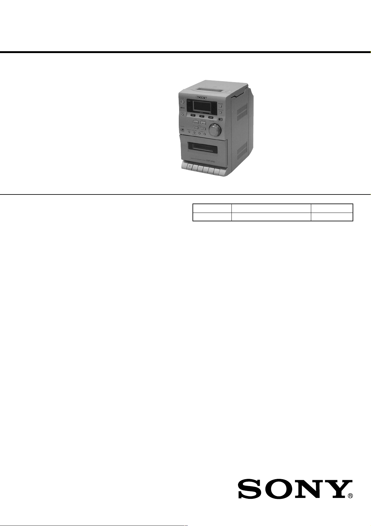
Photo: HCD-EP40
CD Section CD Mechanism Type CS-21SC-1280
TAPE Section Tape Transport Mechanism Type TCM125-2
SPECIFICATIONS
audio system
(λ=780 nm)
Emission duration:
continuous
using Sony TYPE I
cassette
(with the interval set at
10 kHz)
531 - 1 602 kHz
(with the interval set at
9 kHz)
531 -1 602 kHz
(with the interval set at
9 kHz)
(with the interval set at
9 kHz)
530 - 1 710 kHz
(with the interval set at
10 kHz)
US Model
Canadian Model
E Model
Australian Model
HCD-EP30
AEP Model
UK Model
HCD-EP30/EP40
General
Power requirements
US, Canadian models: 120 V AC, 60 Hz
AEP, UK models: 230 V AC, 50/60 Hz
Australian model: 230 V AC, 50/60 Hz
Mexican model: 120 V AC, 60 Hz
Argentine model: 220 V AC, 50/60 Hz
Taiwan model: 110 V AC, 60 Hz
Other models: 230 V AC, 50/60 Hz
Power consumption
US model: 25 W
Canadian model: 25 W
AEP, UK models: 30 W
Other models: 30 W
Dimensions (w/h/d):
Mass: Approx. 2.8 kg
Design and specifications are subject to change
without notice.
0.9 W (in the standby
mode)
Approx. 145 × 238 × 238 mm
9-873-867-11 Sony Corporation
2001D0500-1 Home Audio Company
C 2001.4 Shinagawa Tec Service Manual Production Group
COMPACT DISC DECK RECEIVER
Page 2

HCD-EP30/EP40
TABLE OF CONTENTS
1. SERVICING NOTES ................................................ 4
2. GENERAL ................................................................... 5
3. DISASSEMBLY
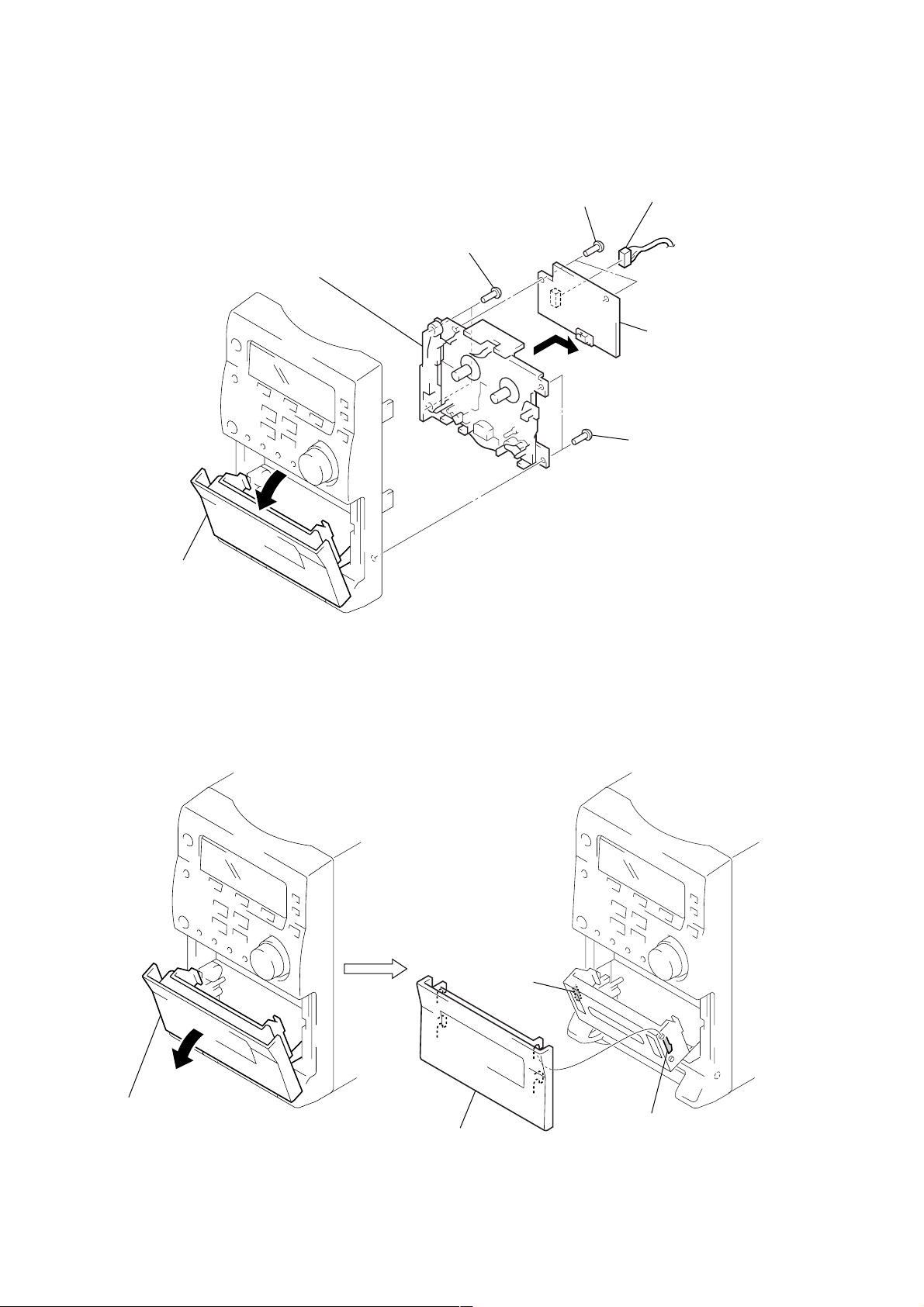
3-1. Disassembly Flow ........................................................... 7
3-2. Front Panel Section ......................................................... 8
3-3. MAIN Board ................................................................... 8
3-4. CD Cabinet Section......................................................... 9
3-5. CD Mechanism Deck (CS-21SC-1280) ......................... 9
3-6. Tape Mechanism Deck (TCM125-2) .............................. 10
3-7. Cassette Lid ..................................................................... 10
4. MECHANICAL ADJUSTMENTS ....................... 11
5. ELECTRICAL ADJUSTMENTS......................... 11
6. DIAGRAMS
6-1. Note for Printed Wiring Boards and
Schematic Diagrams ....................................................... 15
6-2. Schematic Diagram – MAIN Board (1/2) – .................. 16
6-3. Schematic Diagram
– MAIN (2/2)/HEADPHONE Boards – ......................... 17
6-4. Printed Wiring Boards
– MAIN/HEADPHONE Boards –.................................. 18
6-5. Printed Wiring Board – CASSETTE Board –............... 19
6-6. Schematic Diagram – CASSETTE Board –.................. 19
6-7. Printed Wiring Board – DISPLAY Board – .................. 20
6-8. Schematic Diagram – DISPLAY Board – ..................... 21
6-9. Schematic Diagram – POWER Board –........................ 22
6-10. Printed Wiring Board – POWER Board –..................... 23
6-11. IC Pin Function Description ........................................... 25
7. EXPLODED VIEWS
7-1. Cabinet Section ............................................................... 26
7-2. Front Panel Section-1...................................................... 27
7-3. Front Panel Section-2...................................................... 28
7-4. CD Cabinet Section......................................................... 29
8. ELECTRICAL PARTS LIST ............................... 30
2
Page 3
HCD-EP30/EP40
r
Notes on chip component replacement
• Never reuse a disconnected chip component.
• Notice that the minus side of a tantalum capacitor may be damaged by heat.
Flexible Circuit Board Repairing
• Keep the temperature of the soldering iron around 270 ˚C during repairing.
• Do not touch the soldering iron on the same conductor of the
circuit board (within 3 times).
• Be careful not to apply force on the conductor when soldering
or unsoldering.
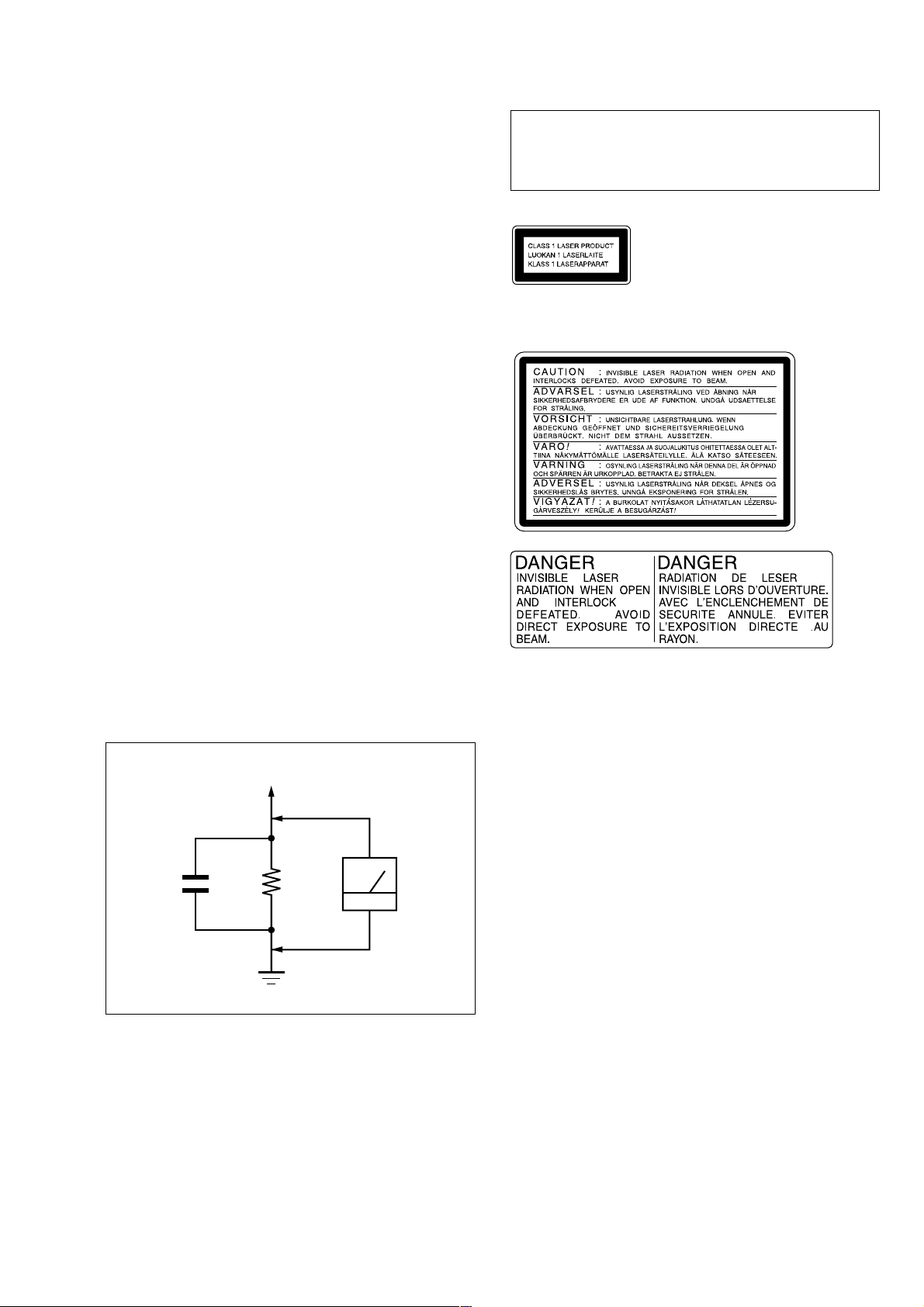
SAFETY CHECK-OUT
After correcting the original service problem, perform the following safety check before releasing the set to the customer:
Check the antenna terminals, metal trim, “metallized” knobs,
screws, and all other exposed metal parts for AC leakage.
Check leakage as described below.
LEAKAGE TEST
The AC leakage from any exposed metal part to earth ground and
from all exposed metal parts to any exposed metal part having a
return to chassis, must not exceed 0.5 mA (500 microamperes.).
Leakage current can be measured by any one of three methods.
1. A commercial leakage tester , such as the Simpson 229 or RCA
WT -540A. Follo w the manufacturers’ instructions to use these
instruments.
2. A battery-operated AC milliammeter. The Data Precision 245
digital multimeter is suitable for this job.
3. Measuring the voltage drop across a resistor by means of a
VOM or battery-operated AC voltmeter. The “limit” indication is 0.75 V, so analog meters must have an accurate lowvoltage scale. The Simpson 250 and Sanwa SH-63Trd are examples of a passive VOM that is suitable. Nearly all battery
operated digital multimeters that have a 2 V A C range are suitable. (See Fig. A)
CAUTION
Use of controls or adjustments or performance of procedures
other than those specified herein may result in hazardous radiation exposure.
This appliance is classified as
a CLASS 1 LASER product.
The CLASS 1 LASER
PRODUCT MARKING is
located on the rear exterior.
The following caution label is located inside the unit.
To Exposed Metal
Parts on Set
1.5 k
0.15 µF
Fig. A. Using an AC voltmeter to check AC leakage.
SAFETY-RELATED COMPONENT WARNING!!
COMPONENTS IDENTIFIED BY MARK 0 OR DOTTED
LINE WITH MARK 0 ON THE SCHEMATIC DIAGRAMS
AND IN THE PARTS LIST ARE CRITICAL TO SAFE
OPERATION. REPLACE THESE COMPONENTS WITH
SONY PARTS WHOSE PART NUMBERS APPEAR AS
SHOWN IN THIS MANUAL OR IN SUPPLEMENTS PUBLISHED BY SONY.
Ω
Earth Ground
AC
voltmete
(0.75 V)
ATTENTION AU COMPOSANT AYANT RAPPORT
À LA SÉCURITÉ!
LES COMPOSANTS IDENTIFIÉS P AR UNE MARQ UE 0
SUR LES DIAGRAMMES SCHÉMATIQUES ET LA LISTE
DES PIÈCES SONT CRITIQUES POUR LA SÉCURITÉ
DE FONCTIONNEMENT. NE REMPLACER CES COMPOSANTS QUE PAR DES PIÈCES SONY DONT LES
NUMÉROS SONT DONNÉS DANS CE MANUEL OU
DANS LES SUPPLÉMENTS PUBLIÉS PAR SONY.
3
Page 4
HCD-EP30/EP40
SECTION 1
SERVICING NOTES
NOTES ON HANDLING THE OPTICAL PICK-UP
BLOCK OR BASE UNIT
The laser diode in the optical pick-up block may suffer electrostatic break-down because of the potential difference generated
by the charged electrostatic load, etc. on clothing and the human
body.
During repair, pay attention to electrostatic break-down and also
use the procedure in the printed matter which is included in the
repair parts.
The flexible board is easily damaged and should be handled with
care.
NOTES ON LASER DIODE EMISSION CHECK
The laser beam on this model is concentrated so as to be focused
on the disc reflective surface by the objective lens in the optical
pick-up block. Therefore, when checking the laser diode emission, observe from more than 30 cm away from the objectiv e lens.
LASER DIODE AND FOCUS SEARCH OPERATION
CHECK
1. Press the I/1 button to the power ON with no disc inserted
and press the [CD] button.
2. Open the lid for CD.
3. Turn on SW600 as following figure.
4. Confirm the laser diode emission while observing the objecting lens. When there is no emission, Auto Power Control circuit or Optical Pick-up is broken.
Objective lens moves up and down five times for the focus
search.
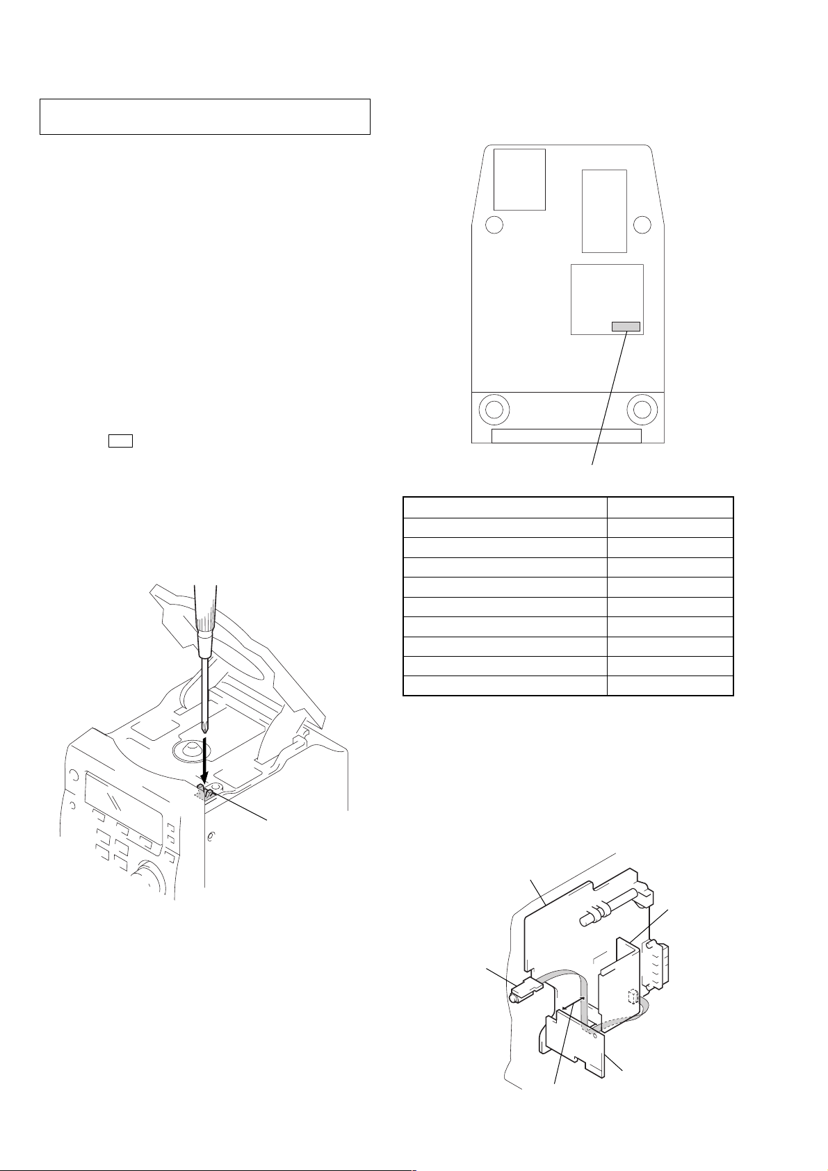
• MODEL IDENTIFICATION
– Bottom View –
PART No.
MODEL PART No.
EP30: AEP and UK models 4-235-167-0
US and Canadian models 4-235-169-0
Singapore model 4-235-170-0
Australian model 4-235-171-0
Taiwan model 4-235-172-0
Mexican model 4-235-173-0
Argentina model 4-235-174-0
EP40: AEP and UK models 4-235-175-0
Saudi Arabia model 4-236-316-0
[]
[]
[]
[]
[]
[]
[]
[]
[]
SW600
TO PREVENT ‘T APE OSCILLATION SOUND AT V OLUME’
MAXIMUM SETTING (W/O TAPE)
Headphone wire dressing:
a.) Draw the wire from Main board to Headphone Jack board along
the bottom side of heatsink.
b.) The wire must be kept away from the top side of Cassette board
at least 30 mm.
MAIN board
heatsink
HEADPHONE
board
CASSETTE board
at least 30 mm
4
Page 5
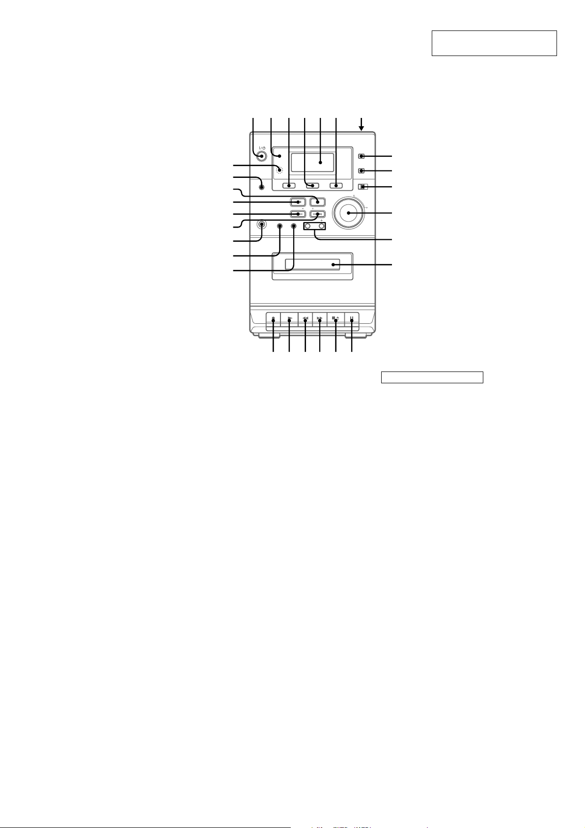
LOCATION OF CONTROLS
– Front Panel –
SECTION 2
GENERAL
1 2 3456 7
HCD-EP30/EP40
This section is extracted from
instruction manual.
wk
wj
wh
wg
wf
wd
ws
wa
w;
Cassette compartment qd (12)
CD 4 (8, 9, 13, 15)
Display Window 5 (9, 18)
ENTER/PGM w; (7, 8, 9, 10, 12,
15)
ISS 0 (13)
MEGA BASS 8 (14)
MONO STEREO 0 (11)
MUSIC MENU 9 (14)
PHONES jack ws
PRESET +/— qs (10, 11)
RDS (CMT-EP40 only) wg (11,
12)
REMAIN 4 (9)
qfqj qhql qk qg
Remote sensor wk
REPEAT wj (8)
SHUFFLE wa (8)
TAPE 3 (12)
TIMER indicator 2 (15)
TUNER 6 (10, 13, 15)
TUNER DSPL (CMT-EP40 only)
wh (11)
TUNER MEM w; (10)
TUNING + wd (10, 11)
TUNING — wf (10, 11)
VOLUME control qa (15)
8
9
q;
qa
qs
qd
BUTTON DESCRIPTIONS
@/1 (power) 1 (6, 10)
CD
. m (go back) wf (8, 9)
M > (go forward) wd (8, 9)
u (play/pause) wg (8, 9)
Z PUSH OPEN/CLOSE 7 (8)
x (stop) wh (8, 9)
TAPE
M (fast forward) qh (12)
X (pause) qf (12, 13)
N (play) qk (12, 15)
z (recording) ql (13)
m (rewind) qj (12)
xZ (stop/eject) qg (12, 13)
5
Page 6
HCD-EP30/EP40
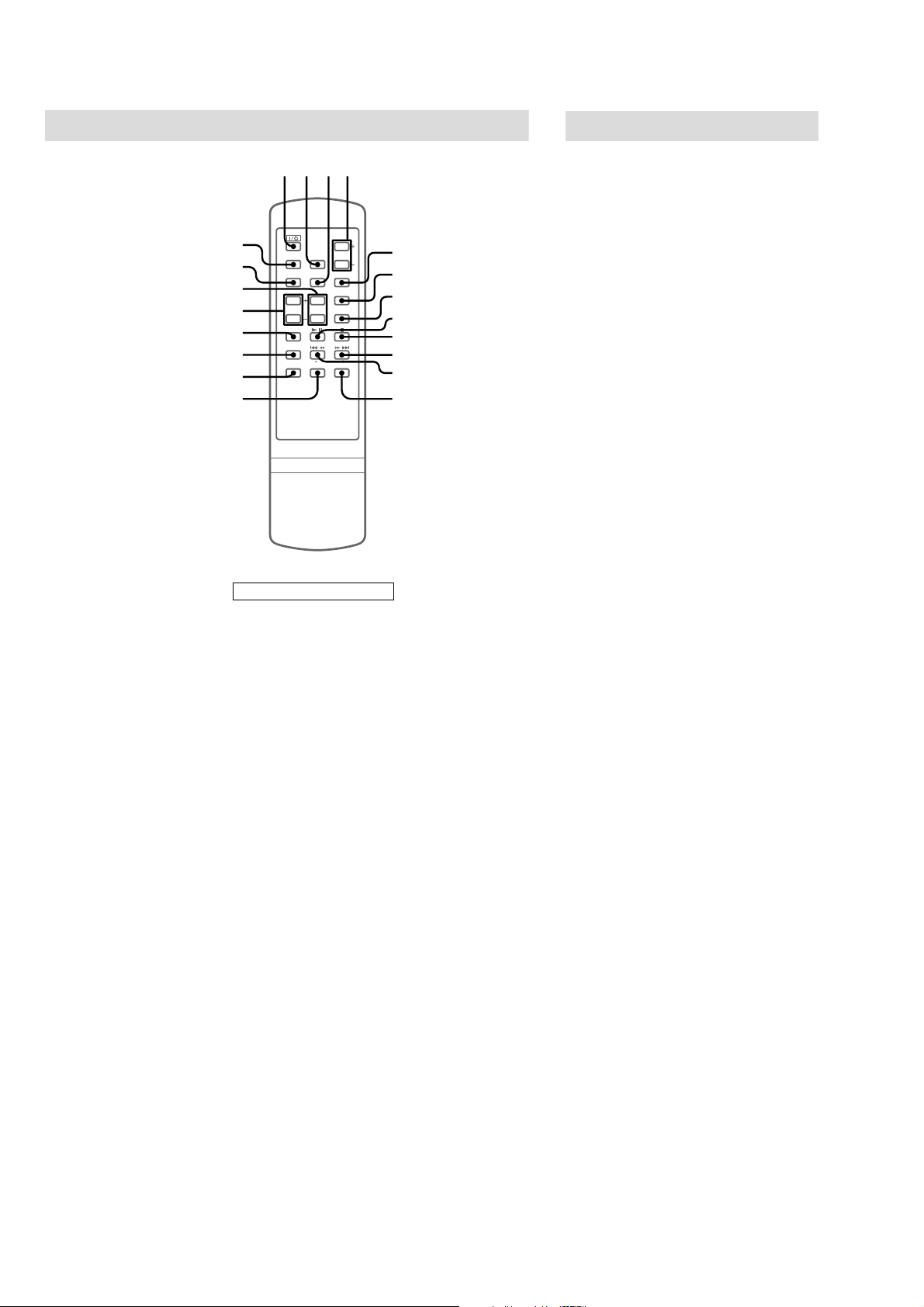
Remote Control
w;
ql
qk
qj
qh
qg
qf
qd
1234
5
6
7
8
9
q;
qa
qs
Setting the time
1 Turn on the system.
2 Press CLOCK/TIMER/SLEEP SET on
the remote.
The clock indication appears.
3 Press TUNING/CLOCK/TIMER + or — on
the remote repeatedly to set the time.
4 Press ENTER/PGM (TUNER MEM/
ENTER/PGM on the remote).
The clock starts working.
Tip
If you made a mistake, perform from step 2.
To change the preset time
Perform from step 2.
Note
The clock settings are canceled when you disconnect
the power cord or if a power failure occurs.
CD/REMAIN 3 (8, 9, 13, 15)
CLOCK/TIMER/SLEEP SET qf
(7, 15)
MEGA BASS 2 (14)
MUSIC MENU w; (14)
PRESET +/— qj (10, 11)
RDS (CMT-EP40 only) qh (11,
12)
REPEAT qs (8)
SHUFFLE 7 (8)
TAPE ql (12)
TIMER ON/OFF qd (15)
TUNER/BAND 5 (10, 13, 15)
TUNER DSPL (CMT-EP40 only)
qg (11)
TUNER MEM/ENTER/PGM 6
(7, 8, 9, 10, 11, 15)
TUNING/CLOCK/TIMER +/—
qk (7, 10, 11, 15)
VOLUME +/— 4 (15)
BUTTON DESCRIPTIONS
M (fast forward) > (go
forward) 0 (8, 9)
. (go back) m (rewind) qa
(8, 9)
u (play/pause) 8 (8, 9)
`/1 (power) 1 (6, 10)
x (stop) 9 (8, 9)
6
Page 7
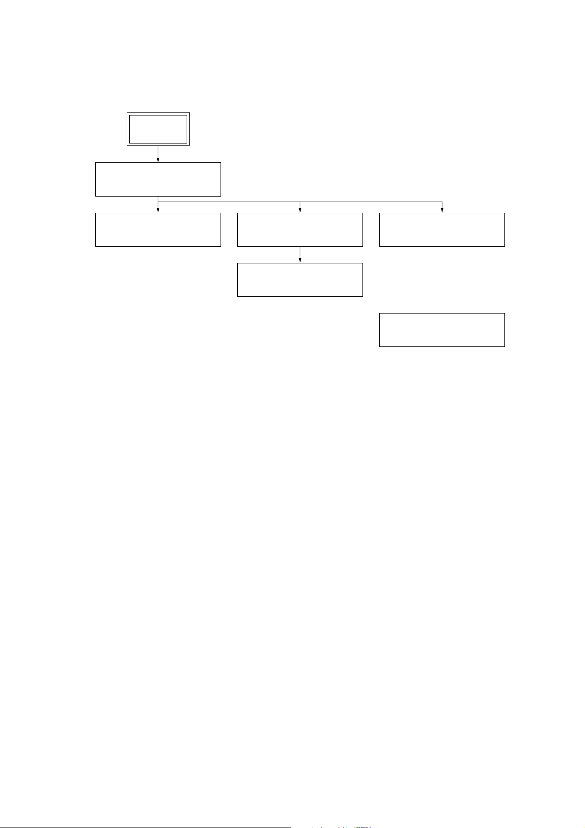
• This set can be disassembled in the order shown below.
3-1. DISASSEMBLY FLOW
SET
3-2. FRONT PANEL SECTION
(Page 8)
HCD-EP30/EP40
SECTION 3
DISASSEMBLY
3-3. MAIN BOARD
(Page 8)
3-4. CD CABINET SECTION
(Page 9)
3-5. CD MECHANISM DECK
(CS-21SC-1280)
(Page 9)
3-6. TAPE MECHANISM DECK
(TCM125-2)
(Page 10)
3-7. CASSETTE LID
(Page 10)
7
Page 8
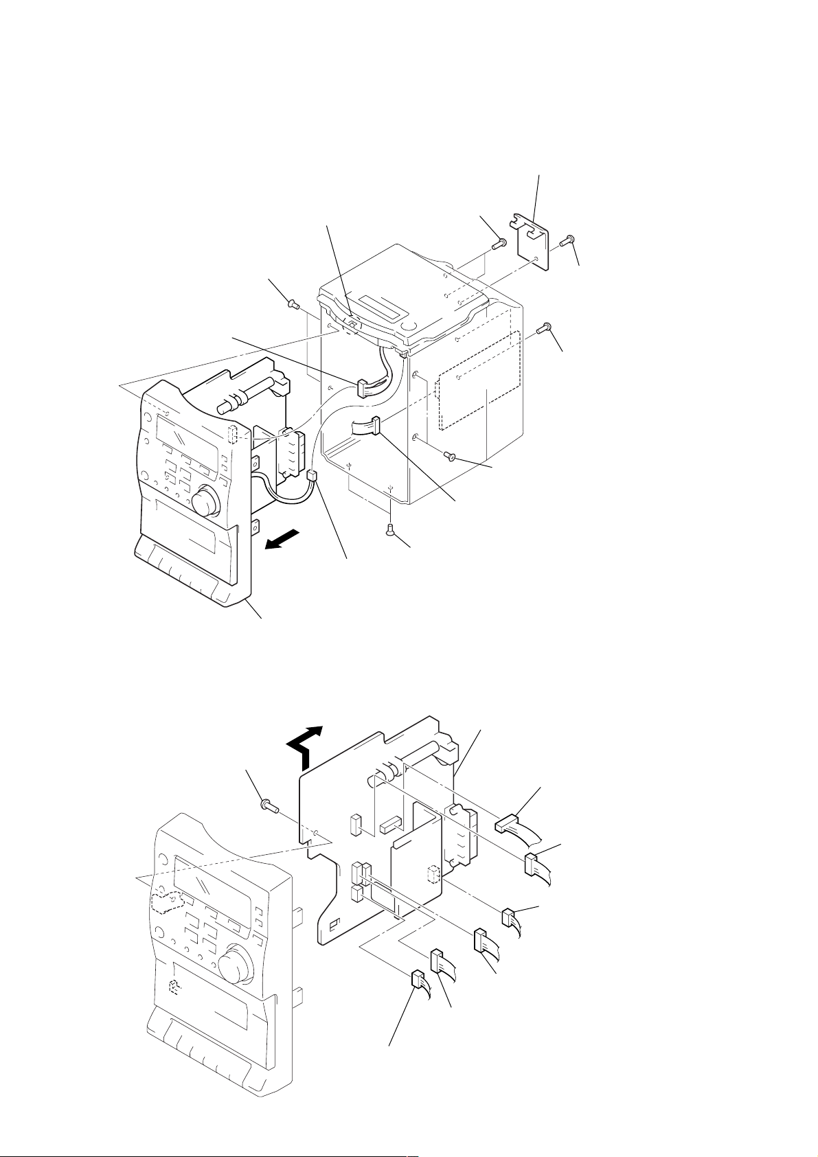
HCD-EP30/EP40
)
r
Note: Follow the disassembly procedure in the numerical order given.
3-2. FRONT PANEL SECTION
6
claw
5
two screws
(+K3
×
5)
8
connector
(CN203)
3
two screws
(BTP2.6
2
antenna cover cabinet
×
10)
1
screw
(BVTP3
4
two screws
(BVTP3
×
×
10)
10
3-3. MAIN BOARD
7
screw
(+BTP2.6 × 8)
7
0
qa
front panel section
8
connector
(SW600)
5
two screws
(+K3
9
connector
(CN402)
×
5)
5
two screws
(+K3
9
MAIN board
×
5)
1
connector
(CN204)
2
connecto
(CN101)
6
connector
(CN202)
5
connector
(CN201)
4
3
connector
(CN302)
connector
(CN301)
8
Page 9
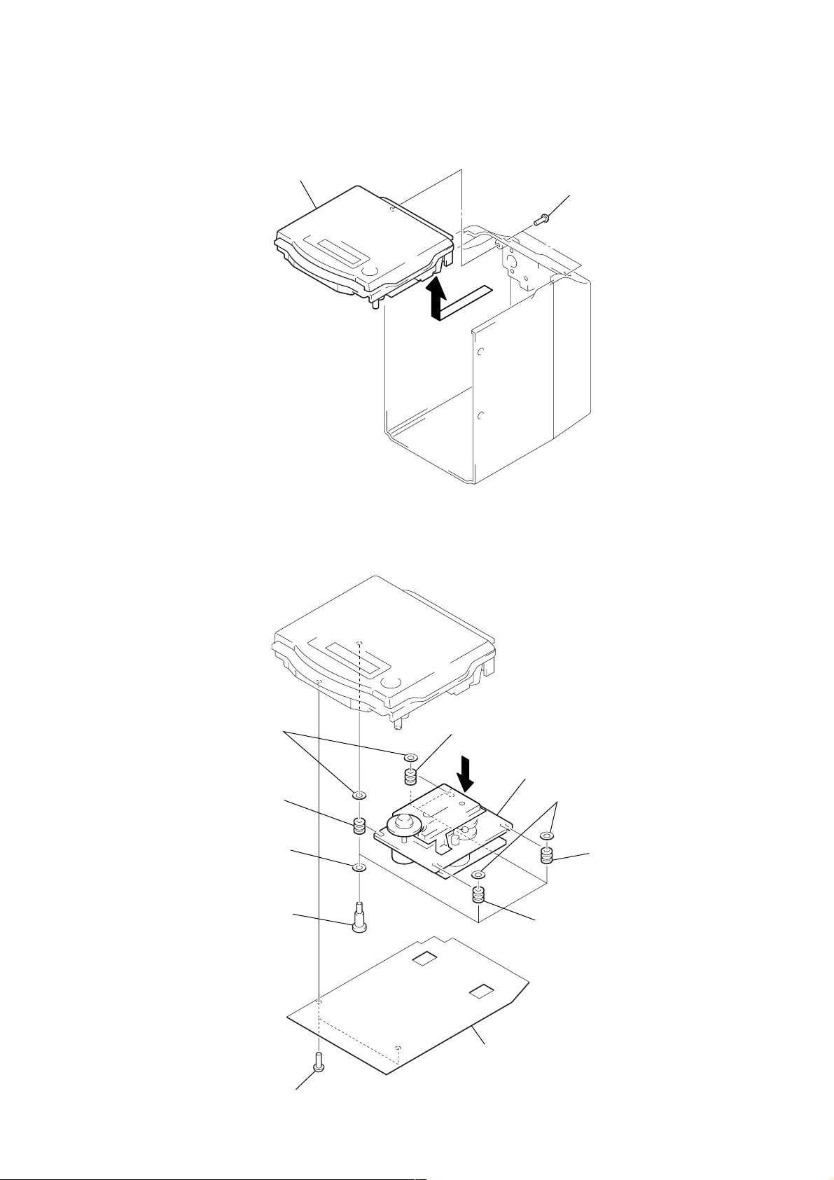
3-4. CD CABINET SECTION
)
2
CD cabinet section
1
two screws
(BTP2.6
HCD-EP30/EP40
×
8
3-5. CD MECHANISM DECK (CS-21SC-1280)
6
two spring clamps
7
vibration proof rubber
(pink)
4
four fiber washers
3
four pulley screws
7
vibration proof rubber
(brown)
5
8
CD mechanism deck (CS-21SC-1280)
6
two spring clamps
7
vibration proof rubber
(brown)
7
vibration proof rubber
(pink)
1
two screws
(BVTP3 × 10)
2
plastic cover
9
Page 10
HCD-EP30/EP40
3-6. TAPE MECHANISM DECK (TCM125-2)
7
tape mechanism deck (TCM125-2)
6
two screws
(BVTP3
×
10)
2
two screws
(BTP2.6
3
1
4
6
two screws
(BVTP3
connector
(CN701)
cassette board
×
10)
×
6)
5
Open the cassette lid.
3-7. CASSETTE LID
2
claw
10
1
Open the cassette lid.
3
cassette lid
2
claw
Page 11
SECTION 4
r
CAPSTAN/REEL
motor (M201)
Tape Speed
Adjustment
MECHANICAL ADJUSTMENTS
HCD-EP30/EP40
SECTION 5
ELECTRICAL ADJUSTMENTS
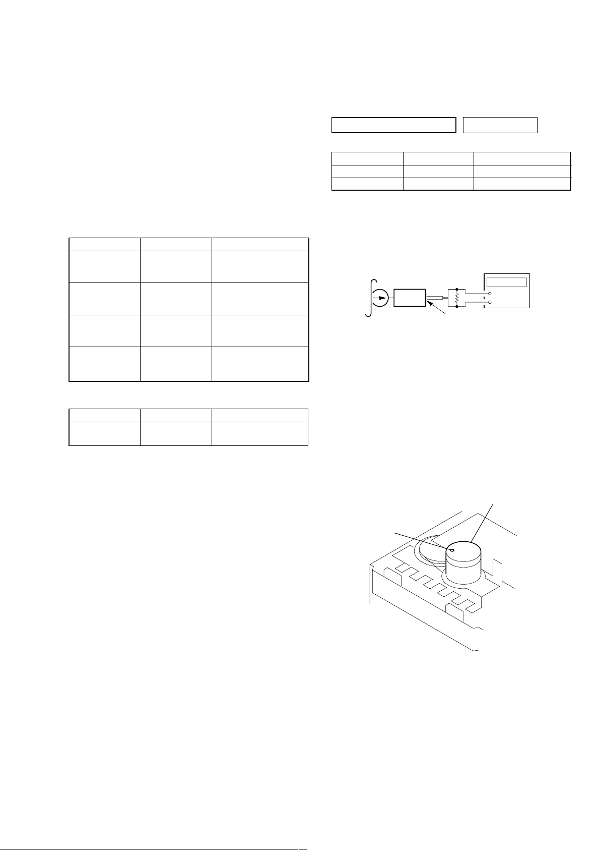
PRECAUTION
1. Clean the following parts with a denatured-alcohol-moistened
swab :
record/playback head pinch roller
erase head rubber belts
capstan idlers
2. Demagnetize the record/playback head with a head demagnetizer. (Do not bring the head magnetizer close to the erase head.)
3. Do not use a magnetized screwdriver for the adjustments.
4. After the adjustments, apply suitable locking compound to the
parts adjusted.
5. The adjustments should be performed with the rated power
supply voltage unless otherwise noted.
• Torque Measurement
Mode Torque Meter Meter Reading
FWD CQ-102C (30 – 70 g•cm)
FWD
Back Tension
FF CQ-201B (more than 60 g•cm)
REW CQ-201B (more than 60 g•cm)
CQ-102C (1.5 – 5.5 g•cm)
• Tape T ension Measurement
Mode Tension Meter Meter Reading
FWD CQ-403A
2.95 – 6.86 mN•m
(0.42 – 0.97 oz•inch)
0.15 – 5.39 mN•m
(0.021 – 0.076 oz•inch)
more than 5.89 mN•m
(more than 0.83 oz•inch)
more than 5.89 mN•m
(more than 0.83 oz•inch)
more than 100 g
(more than 3.53 oz)
PRECAUTION
1. Setting
MEGA BASS switch : OFF
TAPE DECK SECTION 0 dB=0.775 V
Test tape
Type Signal Used for
WS-48A 3 kHz, 0 dB Tape Speed Adjustment
P-4-A063 6.3 kHz, –10 dB Head Azimuth Adjustment
Tape Speed Adjustment
Setting:
Function: TAPE
test tape
WS-48A
(3 kHz, 0 dB)
set
Procedure:
1. Playback WS-48A (tape center) in the FWD state.
2. Adjsut the volume in CAPST AN/REEL motor (M201) so that
the frequency counter reading becomes 3,000 Hz.
Specified Value: 2,985 to 3,015 Hz
3. Confirm that the frequency at the beginning and that at the
end of tape winding are between 2,955 to 3,045 Hz.
frequency counte
32
Ω
+
–
HEADPHONE board
PHONES jack (JK401)
Adjustment Location:
11
Page 12
HCD-EP30/EP40
Record/Playback Head Azimuth Adjustment
Procedure:
1. Mode: Playback (FWD)
test tape
P-4-A063
(6.3 kHz, –10 dB)
set
HEADPHONE board
PHONES jack (JK401)
32
level meter
Ω
+
–
2. Turn the adjustment screw and check output peaks. If the peaks
do not match for L-CH and R-CH, turn the adjustment screw
so that outputs match within 1dB of peak.
Output
level
within
1dB
L-CH
peak
R-CH
peak
within
1dB
Screw
position
L-CH
peak
Screw
position
R-CH
peak
Adjustment Location:Record/Playback/Erase Head.
Note: Refer to “3-7. CASSETTE LID” (see page 10)
3. Mode: Playback (FWD)
test tape
P-4-A063
(6.3 kHz, –10 dB)
L-CH
set
R-CH
in phase
32
32
HEADPHONE board
PHONES jack (JK401)
screen pattern
45
°
90
good wrong
Ω
Ω
135 °180
°
oscilloscope
V
H
+
+
–
–
°
4. Repeat step 1 to 3 in playback (REV) mode.
5. After the adjustments, apply suitable locking compound to the
parts adjusted.
12
Page 13

HCD-EP30/EP40
)
)
TUNER SECTION 0 dB=1 µV
[AM]
Setting:
Function : TUNER
Band switch: AM
AM RF signal
generator
30% amplitude
modulation by
400 Hz signal
Output level: as low as possible
[FM]
Setting:
Function : TUNER
Band switch: FM
FM RF signal
generator
22.5 kHz frequency
deviation by 400 Hz
signal
Output level: as low as possible
Put the lead-wire
antenna close to
the set.
set
MAIN board
0.01 µF
FM ANT
set
level meter
32
Ω
+
–
HEADPHONE board
PHONES jack (JK401
level meter
32
Ω
+
–
HEADPHONE board
PHONES jack (JK401
no mark: US, Canadian, E, Australian models
< > : AEP, UK models
AM FREQUENCY COVERAGE ADJUSTMENT
Adjustment Part Frequency Display Reading on Digital Voltmeter
Confirmation
T102
Adjust for a maximum reading on level meter
L110 600 kHz <603 kHz>
TC102 1,400 kHz <1,404 kHz>
FM FREQUENCY COVERAGE ADJUSTMENT
Adjustment Part Frequency Display Reading on Digital Voltmeter
L104 87.6 MHz 2.1 ± 0.2 V
Confirmation 108 MHz 7.0 ± 0.4 V
Adjust for a maximum reading on level meter
L103 89.9 MHz
TC101 105.9 MHz
530 kHz
<531 kHz>
1,710 kHz 7.7 ± 0.3 V
<1,602 kHz> <7.3 ± 0.3 V>
AM TRACKING ADJUSTMENT
FM TRACKING ADJUSTMENT
1.5 ± 0.2 V
Adjustment Location: MAIN board (See page 14)
digital voltmeter
MAIN board
TP10 (FM VT)
TP11 (AM VT)
100 k
Ω
• Repeat the procedures in each adjustment several times, and the
frequency coverage and tracking adjustments should be finally
done by the trimmer capacitors.
13
Page 14

HCD-EP30/EP40
t
Adjustment Location and Connecting Points
– MAIN BOARD (Component Side) –
L104 FM Frequency
Coverage Adjustment
T102
AM Tracking
}
TP10
(FM VT)
TC102
L110 Adjustment
AM Frequency Coverage Adjustment
– MAIN BOARD (Conductor Side) –
L103
TC101
IC101
TP11
(AM VT)
FM Tracking Adjustmen
}
14
Page 15

SECTION 6
DIAGRAMS
HCD-EP30/EP40
6-1. NOTE FOR PRINTED WIRING BOARDS AND SCHEMATIC DIAGRAMS
Note on Printed Wiring Board:
• W : indicates side identified with part number.
• : Pattern from the side which enables seeing.
(The other layers' patterns are not indicated.)
Note on Schematic Diagram:
• All capacitors are in µF unless otherwise noted. pF: µµF
50 WV or less are not indicated except for electrolytics
and tantalums.
• All resistors are in Ω and 1/
specified.
• 2 : nonflammable resistor.
• C : panel designation.
Note:
The components identified by mark 0 or dotted
line with mark 0 are critical for safety.
Replace only with part
number specified.
• A : B+ Line.
• H : adjustment for repair.
• Voltages are taken with a VOM (Input impedance 10 MΩ).
Voltage variations may be noted due to normal production tolerances.
• Waveforms are taken with a oscilloscope.
Voltage variations may be noted due to normal production tolerances.
• Circled numbers refer to waveforms.
• Signal path.
F : FM
f : AM
E : T APE PLAY
a : RECORD
J : CD PLAY
• Abbreviation
AUS : Australian model
CND : Canadian model
4
Note:
Les composants identifiés par
une marque 0 sont critiques
pour la sécurité.
Ne les remplacer que par une
pièce portant le numéro
spécifié.
• Circuit Boards Location
MAIN board
W or less unless otherwise
HEADPHONE board
POWER board
CASSETTE board DISPLAY board
1515
Page 16

HCD-EP30/EP40
6-2. SCHEMATIC DIAGRAM – MAIN Board (1/2) –• See page 23 for Waveforms. • See page 24 for IC Block Diagrams.
FM
LEAD
ANTENNA
ANT1
FM ANT
75Ω
COAXIAL
MAIN BOARD
C104
0.001
C157
0.1
1N4148TP
1N4148TP
0.047
AM FERRITE-ROD
(1/2)
L103, TC101
FM TRACKING
C105 0.001
L103
FM RF
1µH
ANTENNA
AM OSC
0.047
1
(0)
1.3
+
L104
FM FREQUENCY
COVERAGE
0.001
5.2 (0)
1.3
5.2 (6.2)
50V
C111
0.001
L104 FM OSC
5.2 (6.2)
5.2 (6.2)
5.2 (6.2)
2.8 (3.6)
0.0015
50V
0 (6.2)
+
0 (0.7)
1.2 (0.4)
0
5.2
(6.2)
TP10
(FM VT)
1.3
5.2
10.7MHz
R112
3.3k
2SC1923
0.0015
(6.2)
1.2k
1.3
Q101
FM OSC BUFFER
5.4
(0.1)
10V
0
4.5 (4.3)
4.5 (0.1)
1.3
1.3
450kHz
+
4.5 (5.6)
10.7MHz
0.3 (0.5)
3.9k
3.9k
2.2P
0.01
0.001
4.5 (4.3)
4.5 (4.3)
IC101
FM/AM IF AMB
MIX, MPX, DET, OSC
IC B/D
IC102
FM/AM PLL
IC B/D
0.01
50V
5.6k
+
2.2k
+
0.1
1
+
50V
+
50V
0
50V
+
+
+
(0.4)
50V
0.2
BUFFER
(5.4)
3.3k
5.2
0.0033
0.0033
Q103
STEREO/MONO
SWITCHING
0 (0.7)
4.5 (0.1)
+
50V
50V
+
470
16V
Q102
FM/AM BAND
SELECT SWITCH
0.047
6.8k
6.8k
100p
0
4.7k
0
1µH
Q116, 209, 210
TUNER B+ SWITCH
Q109, 605
B+ SWITCH
0.1
0.001
0.022
0 (2.6)
2.6 (0)
0.1 (3.1)
5.6k
5.1
0.9
0
5.4
2.6
0.9
2.4 (1.5)
2.5
0.1
0.1
10V
+
5.4
7.2MHz
0
0
0.1
+
16V
9.2
0.7
MTZJ-5.1
9.3
8.5
0
CN101
8P
RDSCL
RDSDA
PLLCE
PLLDI
PLLCL
STOUT
SIG
CT
A
DSIPLAY
BOARD
(Page 21)
L110, TC102
AM TRACKING
T102
AM FREQUENCY
COVERAGE
TP11
(AM VT)
0.022
0.022
+
0
2.4
4.5
MUX
VREF
VSS1
VDD1
VDD2XIXONCRCLK
1.6
4.5
+
2.2
16V
50V
2.4
*
RDAT
QUAL
2
2.2
2.2
U
4
u
5.6
4.7k
5.4
2SD1616-L
4.8
100µH
+
0.1
IC604
RDS DECODER
EP40
U
U
U
2
3
1
u
u
u
IC B/D
0.1
1
2.4
MAIN BOARD
(2/2)
0
CMP
VSS3
T2T1VSS2
(Page 17)
• Voltages and waveforms are dc with respect to ground
under no-signal (detuned) conditions.
no mark : FM
( ) : AM
: Impossible to measure
∗
1616
Page 17

6-3. SCHEMATIC DIAGRAM – MAIN (2/2)/HEADPHONE Boards –• See page 24 for IC Block Diagram.
MAIN BOARD
(1/2)
(2/2)
2200p
(Page 16)
4700p
U
4
u
3.3k
3.3k
0.0033
0.1
0.1
0.1
0.0082
5.3
4.8
7.8
3.9
0.1
+
16V
0
0
0
0
0.0082
0.1
0.1
0.1
0.0033
0.047
8.2k
5.6k
0.0039
0.027
3.9
3.9
3.9
3.6
3.6
3.9
3.9
0.027
0.0039
5.6k
0.047
3.9
8.2k
MTZJ-6.2B
3.9
3.9
3.9
3.9
13.5
2SD1616-L
+
Q312
+6V REGULATOR
3.9
3.9
3.9
5.66.2
(Page 19)
M201
(CAPSTAN/REEL)
B
CASSETE
BOARD
S201
(PLAY)
BEAT
GND
SYNC
COTR
1
U
U
U
1
2
3
u
u
u
CN201
9P
RL
RR
PL
PR
9V
16V
0.1
CN202
4P
MAIN BOARD
0.047
3.9k
3.9k
Q201, 202
REC AMP
+
+
2.1
1.4
1.4
2.1
+
1.9
50V
1.9
+
1 50V
+
16V
IC203
FUNCTION SELECT SWITCH,
ELECTRICAL VOLUME
IC B/D
4.7
50V
+
+
50V
+
3.9
50V
3.9
3.9
+
50V
+
4.7
50V
+
1N4148TP
4.7
50V
0.001
+
6.8k
8.2k
6.8k
50V
0.001
Q205, 206
MEGA BASS
ON DRIVE
8.2k
50V
0.022
+
3.3k
2.2k
4.7k
4.7k
2.2k
3.3k
+
9.3
9.9
+
50V
+9V REGULATOR
0
MEGA BASS
ON : 0.1
OFF : 0.7
MEGA BASS
ON : 0.1
OFF : 0.7
0
13.7
Q313
CD –SW
6V
+
MTZJ-10B
(Page 21)
DISPLAY
C
TU –SW
TA –SW
1N4148TP
+
10V
BOARD
LED V+
0.022
GND
PSW
MUTE
9K/10K
0.8 (9.5)
1N4148TP
+
9P
1N4148TP
1N4148TP
50V
2SD1616-L
+
2SD1616-L
+9V REGULATOR
0.8
(10)
13.6
(0)
REGULATOR CONTROL
1N4148TP
0 [0.6]
0
0
0 [0.6]
Q301, 302
MUTING
Q308, 309
13.7
0.6 (13.6)
4.7k
MTZJ-10B
Q310, 311
SWITCH
[0.6]
9P
0
BEAT
SYNC
MUTING CONTROL
SWITCH
0 [1.1]
13.7
13.6
(12.9)
0
(0.7)
(Page 21)
DISPLAY
D
BOARD
CE
DBBS
Q314
1N4148TP
0.001
+
+
0.001
50V
0.6
(0)
CLK
HCD-EP30/EP40
SUPPLIED AS THE
CD
*
*
ASSEMBLED BLOCK
BLOCK
CDDATA
CDCLK
CDRS
DAT
9P
2200p
+
16.1
8.7
8.7
16.1
++
0.1
1N4148TP
AM FREQ STEP
10 kHz
R
9 kHz
+
25V
25V
2.7k
2.7k
IC301
POWER AMP
50V
0
+
0.6
16V
16V
0.6
+
0
16.4
1N4148TP
0.022
HEAT OPERATION
PROTECTION CIRCUIT
+
13.7
13
0.3
B+ SWITCH
BIAS CIRCUIT,
Q305, 306
+
8.7
+
–
–
+
16.7
13.7
+
0.7
50V
HEADPHONE BOARD
5
CN301
5P
0.15
0.15
+
1N4148TP
1N4148TP
1
2
3
4
5
6
7
1
+
–
–
+
6
1
PHONES
DC_15V
R
L
SPEAKER
IMPEDANCE
USE 4Ω
POWER
BOARD
(Page
E
CN402
22)
• Voltages are dc with respect to ground under no-signal
(detuned) conditions.
no mark : TUNER (FM/AM)
( ) : CD PLAY
[ ] : TAPE PLA Y
1717
Page 18

HCD-EP30/EP40
• Semiconductor
Location
Ref. No. Location
D101 B-4
D102 B-5
D103 B-8
D104 C-9
D105 B-5
D302 G-6
D303 G-6
D306 F-6
D307 H-8
D308 G-7
D310 H-8
D311 H-8
D312 F-6
D314 F-7
D316 F-6
D317 H-8
IC101 B-9
IC102 D-8
IC203 D-5
IC301 G-5
IC604 E-8
Q101 D-9
Q102 C-10
Q103 B-10
Q104 A-10
Q109 C-8
Q116 D-10
Q201 D-4
Q202 E-4
Q205 F-4
Q206 D-4
Q209 E-8
Q210 E-9
Q301 F-5
Q302 F-6
Q305 H-6
Q306 G-7
Q308 H-7
Q309 H-7
Q310 G-8
Q311 G-7
Q312 G-7
Q313 H-7
Q314 G-6
Q605 G-7
ZD103 E-9
ZD302 H-7
ZD304 H-6
ZD305 G-7
6-4. PRINTED WIRING BOARDS – MAIN/HEADPHONE Boards –• See page 15 for Circuit Boards Location.
1 2 3 4 5 6 7 8 9 10
L110
AM FERRITE-ROD
ANTENNA
A
MAIN BOARD
AKA
B
FM LEAD
ANTENNA
AKAK
ANT101
FM ANT
75Ω
COAXIAL
C
+
ECB
D
E
* SUPPLIED AS THE
ASSEMBLED BLOCK
*CD
BLOCK
SW301
FM FREQ
STEP
9 kHz
r
10kHz
++
ECB
+
BCE
++
+
+
++
ECB
+
IC203
+
ECB
+
BCE
+
+
F
HEADPHONE BOARD
7
JK401
PHONES
G
H
34561
2
R413
R412
15
SPK301
SPEAKER
(IMPEDANCE USE 4Ω)
+
L
–
IC301
–
R
+
++
+
+
+
+
+
++
ECB
++
AKAAK
K
A
K
ECB
A
A
KKK
+
A
++
I
1818
T102
OSC
ECB
+
+
+
ECB
ECB
(Page 19)
(Page 20)
1
2
3
4
BCE
DISPLAY
A
(Page 20)
DISPLAY
D
(Page 20)
M
BOARD
BOARD
S201
(PLAY)
M201
(CAPSTAN/REEL)
AM
123
++
16 9
(EP40)
KA
L103
FM RF
TP10
(FM VT)
ECB
TP11
(AM VT)
ECB
IC102
ECB
+
+
KA
+
U04
FM OSC
+
+
IC101
+
BCE
+
+
+
AK
IC604
18
+++
(EP40)
A
K
ECB
BCE
(EP40)
+
BCE
+
K
BCE
AK
ECB
A
BCE
BCE
ECB
+
1
6
+
K
K
K
A
A
A
A
K
B
C
CASSETTE
BOARD
DISPLAY
BOARD
E
POWER BOARD
CN402
(Page 23)
Page 19

6-5. PRINTED WIRING BOARD – CASSETTE Board – • See page 15 for Circuit Boards Location. 6-6. SCHEMATIC DIAGRAM – CASSETTE Board –
• See page 23 for Waveforms. • See page 24 for IC Block Diagram.
1 2 3 4 5
HCD-EP30/EP40
A
HPRE701
REC/PB/ERASE
HEAD
B
C
• Semiconductor
Location
Ref. No. Location
D701 B-4
D702 B-4
+
ECB
CASSETTE BOARD
–1
–2
–3
–4
–5
–6
ECB
SW701
(REC/PB)
REC
PB
CASSETE BOARD
50V
50V
5.6k
3.9
3.9
5.6k
0.0068
1.2k
ALC
IN1
ALC
IN2
0
1.2k
0.022
SW701 (5/6)
(REC/PB)
0.1
0
ALC
CONST
RF
7.7
0.1
SW701 (1/6)
(REC/PB)
REC
R
PB
REC BIAS OSC
9.3 (0.8)
9.3 (0.8)
0
2
REC
r
PB
7.8
Q706
3
IC701
ALC, REC/PB AMP
+
50V
50V
0.022
+
+
+
50V
2SD1616-L
8.9 (0.3)
SW701 (6/6)
(REC/PB)
REC T PB
3
IC B/D
+
50V
1SS133T
-77
MUTING
CONTROL
SWITCH
Q701, 702
MUTING
0 (0.7)
0 (0.7)
100k
0
+
BCE
+
++
+
+
ECB
A
+
MAIN BOARD
B
CN201
(Page 18)
HRPE701
RECORDE/PLAYBACK
ERASE
L-CH
K
IC701
+
+
K
+
+
BCE
+
ECB
A
+
R-CH
ERASE
CN701
4P
SW701 (3/6)
SW701 (4/6)
SW701 (2/6)
(REC/PB)
REC t PB
1
0 (0.7)[0]
(REC/PB)
REC
R
PB
0.0015
(REC/PB)
REC
r
PB
0.0018
0.0018
0.0018
Q705
ISS SWITCHING
0.022
0.1
+
0
IN1 NF1 PC1 OUT1 GND
IN2 NF2 PC2 OUT2 VCC
0
1.2
+
0.0027
0.4 (0)
[21.4]
0.022
+
1.2
1.4
1.4
+
0.1
330
+
50V
0
0
1N4148TP
25V
0.7 (0)
Q704
REC ON SWITCH
0.7
50V
+
+
50V
B
MAIN
BOARD
(2/2)
CN201
(Page 17)
4.7k
0
(3.5)
IC701 B-3
Q701 A-4
Q702 B-4
Q703 B-4
Q704 A-2
Q705 B-2
Q706 C-2
• Voltages and waveforms are dc with respect to ground
under no-signal conditions.
no mark : TAPE PLAY
( ) : RECORD (ISS 1)
[ ] : RECORD (ISS 2)
1919
Page 20

HCD-EP30/EP40
• Semiconductor
Location
Ref. No. Location
D11 F-4
D12 F-4
D13 F-4
D14 F-4
D15 F-3
D16 F-3
D17 F-3
D18 F-2
D19 F-2
D601 C-6
D602 D-5
D603 C-6
D604 C-3
D607 B-3
D608 B-3
D609 D-2
D610 D-2
D611 D-2
D612 C-3
D613 D-3
D614 D-3
D615 D-3
D616 D-6
D617 E-2
D618 D-4
D619 B-6
D647 C-6
D648 D-6
IC601 B-4
IC602 D-2
IC603 A-3
Q601 B-6
Q602 B-6
Q603 D-3
Q604 C-6
REM601 B-6
6-7. PRINTED WIRING BOARD – DISPLAY Board –• See page 15 for Circuit Boards Location.
1 2 3 4 5 6 7
DISPLAY BOARD
A
IC603
1 36
13
D621
LIQUID CRYSTAL DISPLAY
180
IC601
20
(AEP, UK)
K
K
A
SW613
TUNER
K
ECB
KA
21
40 41
A
US, CND,
E, AUS
US, CND,
E, AUS
+ –TUNING
M > m .
D
B
C
MAIN BOARD
CN302
C
(Page 18)
SW614
MUSIC MENU
SW631
(MONO STEREO)
ST t MONO
ISS
2 t 1
SW600
Z PUSH
OPEN/CLOSE
SW622 SW621
+ –VOLUME
MEGA BASS
A
A
A
+
IC602
K
98
K
K
+
116
KA
A
12
K
A
KA
KA
TIMERD619
I/1
REM601
US,
13
BCE
A
A
K
K
ECB
+
K
A
+
AEP, UK,
E, AUS
ECB
K
A
K
US, CND,
E, AUS
A
REPEAT
A
MAIN BOARD
CN101
(Page 18)
SW601 – 615
61
60
+
REMAIN
CD
K
A
TAPE
CND
A
K
E
+ –
D
MAIN BOARD
CN204
(Page 18)
F
(INCLUDED IN DISPLAY BOARD)
R421
D19 D18
R420
D17 D16 D15 D14 D12
D11 – 19
(LCD BACK LIGHT)
(EP40)
PRESET SHUFFLE
SW608
TUNER DSPL
x
R419
D13
D11
2020
21
SW610
RDS
u
TUNER MEM
ENTER PGM
(EP40)
Page 21

6-8. SCHEMATIC DIAGRAM – DISPLAY Board –• See page 23 for Waveform.
DISPLAY BOARD
HCD-EP30/EP40
A
MAIN
BOARD
(1/2)
CN101
(Page 16)
SEL2215S-CD
D619
TIMER
D604
1N4148AP
1N4148TP
1N4148TP
1N4148TP
1N4148TP
1.8k
2.4
0 (4.7)[4.7]
1.4 (0)[1.4]
(AEP, UK)
0
2.4
0 (4)[0]
0 0.6
1.8k
LIQUID CRYSTAL DISPLAY
2.4
2.4
S31
S30
S29
S28
S27
S26
S25
S24
S23
S22
S21
S20
S19
S18
S17
S16
S15
COM0
2.4
COM1
COM2
COM3
4.7
BIAS
4.7
VLC0
3.2
VLC1
1.6
VLC2
TUNER
TAPE
CD
4.6
TIMER STATUS
VSS
4.6
CD RESET
4.5
SURROUND
0
PLL CL
5.3
PLL DI
5.2
TUNER SD
4.7
CLOCK
5.3
DATA
CD CLOCK
STEREO
5.2
2.2
5.3
SYSTEM CONTROLLER
LIQUID CRYSTAL DISPLAY DRIVER
UPD753016AGC-F31-3B9
MUTE
SYNCRO
REMOTE
RDS CLOCK
0
0
5.2
0 {3.5}
PLLCE
0
IC601
MEGA BASS
ON : 0.1
OFF : 4.7
SHRST
CE
*
D616
1N4148TP
2.4
PSW
RDS DATA
4.7
DPSW2/SLEND
BASS BOOST
0
4.7
VDD
S14
12/24H SELECT
X1ICXT2
XT1
4.7
2.4
2.9
+
10
16V
S13
CPU RESET
KEY R3
KEY R2
KEY R1
KEY R0
CD
PLLDO
SELECT
DATA
X2
0.1
S12
S11
S10
S9
S8
S7
S6
S5
S4
S3
S2
S1
S0
NC
2.4
2.4
2.4
2.4
2.4
2.4
2.4
2.4
2.4
2.4
2.4
5.6
5.2
5.2
5.2
5.2
4.3
4.6
5.2
0.1
2.4
(US, CND, E, AUS)
1
+
1000
6.3V
1N4148TP
IC603
RESET SIGNAL
GENERATOR
IC603
P5290
5.6
O
G
0.0022
I
16V
SW601
I /1
5.6
SW621
SW622
SW612
TAPE
SW621 SW622
–
VOLUME
+
SW605
SW606
SW605 SW606
–
PRESET
SW609
TUNING –
. m
TUNING +
M >
1N4148TP
1N4148TP
1N4148TP
1N4148TP
SW607
SW604
TUNER MEM
ENTER PGM
5.3
5.3
5.3
5.3
5.3
4.7
5.3
5.3
5.3
SW613
TUNER
SW614
MUSIC
+
MENU
SW615
MEGA
+
BASS
5.3
5.3
5.3
5.3
1N4148TP
1N4148TP
1N4148TP
10V
SW611
REMAIN
CD
SW602
REPEAT
SW603
SHUFFLE
+
0.1
SW608
TUNER DSPL
x
SW610
(EP40)
(EP40)
RDS
u
IC602
(AEP, UK, E, AUS)
(US, CND, E, AUS)
0 5.6
0
0 0.1
0 5.6
(US, CND)
2.2k
4.7
5.2
0.6
0.1
BUFFER
0.6
+
1N4148TP
10V
5.2
5.2
Q602
POWER
ON/OFF
SWITCH
REM601
REMOTE
CONTROL
RECEIVER
REM601
RPM6938
180
180
L934SGC/B
L934SGC/B
L934SGC/B
L934SGC/B
L934SGC/B
KEY CONTROL
L934SGC/B
L934SGC/B
0.1
(MONO STEREO)
ST t MONO
ISS
2 t 1
9
MAIN BOARD (2/2)
C
CN302
(Page 17)
180
0.1
1
9
D
MAIN BOARD (2/2)
CN204
1
0.1
SW600
ZPUSH
OPEN/CLOSE
L934SGC/B
(LCD BACK LIGHT)
L934SGC/B
D11-19
(Page 17)
• Voltages and waveforms are dc with respect to ground
under no-signal (detuned) conditions.
no mark : FM
< > : AM (9 kHz STEP)
〈〈 〉〉 : AM (10 kHz STEP)
( ) : CD PLAY
[ ] : TAPE PLA Y
{ } : RECORD
: Impossible to measure
2121
∗
Page 22

HCD-EP30/EP40
6-9. SCHEMATIC DIAGRAM – POWER Board –
POWER BOARD
Q404
+6V REGULATOR
6.2
8050D
6.7
7.9
TR402
POWER
TRANSFORMER
C421 0.001 250V
E
MAIN BOARD
(2/2)
CN304
(Page 17)
B GND
CN402
6P
+
MTZJ-6.8B
+
++
RL401
0
0.6
C404 0.022
+
(AEP, UK, E, AUS)
3.15A 125V
(US, CND)
C402 0.022
C408 0.022
2A 125V (US, CND)
+
POWER
TRANSFORMER
(AEP, UK, E, AUS)
TR401
2.2k
Q401–403
POWER ON/OFF
RELAY DRIVE
1.1
0.5
2.2k
1.1
1.1
0.7
8050D
AC IN
C406 0.022
• Voltages are dc with respect to ground under no-signal
conditions.
no mark : TUNER (FM/AM)
The components identified by mark 0 or dotted
line with mark 0 are critical for safety.
Replace only with part number specified.
Les composants identifiés par une marque 0 sont
critiques pour la sécurité. Ne les remplacer que
par une pièce portant le numéro spécifié.
2222
Page 23

HCD-EP30/EP40
6-10. PRINTED WIRING BOARD – POWER Board –• See page 15 for Circuit Boards Location.
1 2 3 4 5
AC IN
A
B
MAIN
BOARD
(Page 18)
E
POWER BOARD
+
A
A
K
KA
+++
BCE
K
A
+
BCE
ECB
BCE
K
A
+
K
K
A
KA
C
KA
AK
AK
D
KA
KA
AK
AK
TR402
POWER
TRANSFORMER
• Waveforms
– MAIN Board –
1 IC102 w; (XOUT)
3.1 Vp-p
139 ns
2 IC604 qf (XO) 2 Q706 (Base) (RECORD mode)
3.2 Vp-p
231 ns
– CASSETTE Board –
1 Q705 (Collector)
(RECORD (ISS 2) mode)
11.8
µ
s
µ
s
12.4
3 Q706 (Collector, Emitter)
(RECORD mode)
– DISPLAY Board –
1 IC601 tl (X2)
4.4 Vp-p
47.2 Vp-p
167 ns
1.3 Vp-p
E
• Semiconductor
Location
Ref. No. Location
D401 D-1
D402 C-1
D403 D-1
D404 C-1
D405 B-2
D406 C-2
D407 B-2
D408 B-2
D409 C-3
D411 C-3
D412 D-3
D413 C-3
D414 D-3
Q401 B-3
Q402 B-3
Q403 B-3
Q404 B-3
ZD401 B-3
TR401
POWER
TRANSFORMER
12.4
0.8 Vp-p
µ
s
2323
Page 24

HCD-EP30/EP40
• IC Block Diagrams – MAIN Board –
IC101 LA1823
FMRF IN
RF GND
FMRF OUT
24 23
FM
RF
AM
RF
1
AMRF IN
GND2
REG
2
REG
22 21
AM
MIX
AM
OSC
3
AM OSC
VCC2
VCC2
OSC
BUFFER
VCC1
4
VCC1
FM OSC
20
FM
OSC
FM
MIX
5 6
FM MIX
19
GND1
DET OUT
MUTE
18 17 16
MUTE
SD
IF
BUFFER
7
GND
FM BUFFER
R
L
AM/FM
15
9
AM MIX
PHASE
COMP
FM
S-METER
FM
IF
10
QUAD
DECODER
ST SW FFVCO FF FF
TRIG
ST
8
AM OSC BUFFER
MO/ST
14
PILOT
DET
AM
DET
AM
IF
11 12
AMIF
FM
DET
13
FM DET
AGC
SD
IC203 LC75392
1
LVROUT
–
+
2
LVRIN
3
LTOUT
4
LTCOM
5
LT4
6
LT3
7
LT2
8
LT1
9
L4
10
L3
11
L2
12
L1
VDD
13
CL
14
15
DI
30
RVROUT
–
+
29
RVRIN
+–+
–
LATCH
DECODER
SHIFT
REGISTER
CONTROL
+
–
28
RTOUT
27
RTCOM
RT4
26
25
RT3
24
RT2
23
RT1
R4
22
R3
21
R2
20
R1
19
VREF
18
VSS
17
16
CE
IC102 LC72131
VSS
2122
INTERFACE
3
2
NC
CCB
4
DI
CE
AOUT
19
20
REFERENCE
DIVIDER
5
6
CL
DO
XOUT
1
XIN
AIN
PD
18
PHASE
DETECTOR
CHARGE PUMP
UNLOCK
DETECTOR
SWALLOW COUNTER
1/16, 1/17 4BITS
12BITS
PROGRAMMABLE
DRIVER
DATA SHIFT REGISTER LATCH
10
7
9
8
BO4
BO2
BO1
BO3
11
POWER
RESET
IO1
NC
AMIN
IO2
VDD
FMIN
17
16
1/2
ON
15
14
13
UNIVERSAL
COUNTER
IFIN
12
VDD2
RCLK
PLL
1187.5Hz
BIPHASE
DECODER
DEFFERENTIAL
DECODER
1 43 65 872
QUAL
NC
PLL 57kHz
RDS/ARI
COMPARATOR
8th SWITCHED
CAPACITOR
FILTER
ANTI-ALIASING
FILTER
RDAT
VREF
MUX
XO
141516 13 121110 9
CLOCK
ANALOG
VSS1
VDD1
VSS3
VSS2
XI
DIGITAL
CMP
T1
TEST
T2
– CASSETTE Board –
IC701 AN7312IC604 BU1924F-E2 (HCD-EP40)
VCC
RF
ALC IN2
14 13 12
RIPPLE FILTER
ALC
1 2 3
GND
ALC CONST
OUT2
11 10 9
AMP. CH2
AMP. CH1
4 5 6 7
OUT1
ALC IN1
PC2
PC1
NF2
NF1
IN2
8
IN1
2424
Page 25

HCD-EP30/EP40
6-11. IC PIN FUNCTION DESCRIPTION
• DISPLAY BOARD IC601 µPD753016AGC-F31-3B9 (SYSTEM CONTROLLER, LIQUID CRYSTAL DISPLAY DRIVER)
Pin No. Pin Name I/O Description
1 to 20 S12 to S31 O Segment drive signal output to the liquid crystal display (D621)
21 to 24 COM0 to COM3 O Common drive signal output to the liquid crystal display (D621)
25 BIAS O Bias output for the liquid crystal display drive
26 to 28 VLC0 to VLC2 I
29 TUNER O Power on/off control signal output for the tuner section “L”: power on
30 TAPE O Audio line muting on/off control signal output “L”: muting on
31 CD O Power on/off control signal output for the CD section “L”: power on
TIMER STATUS
32
33 VSS — Ground terminal
34 CD-RESET O Reset signal output to the CD section “L”: reset
35 SURROUND O Not used (pull up)
36 PLL CL O PLL serial data transfer clock signal output to the FM/AM PLL (IC102)
37 PLL DI O PLL serial data output to the FM/AM PLL (IC102)
38 TUNER SD I FM and AM signal meter voltage detection input from the LA1823 (IC101)
39 CLOCK O Serial data transfer clock signal output to the LC75392 (IC203)
40 DATA O Serial data output to the LC75392 (IC203)
41 STEREO I FM stereo detection signal input from the LA1823 (IC101) “L”: stereo
42 CD CLOCK I Serial data transfer clock signal input from the CD section
43 RDS CLOCK I
44 REMOTE I Remote control signal input from the remote control receiver (RM601)
45 SYNCRO I Recording on detection signal input
46 MUTE O Audio line muting on/off control signal output “H”: muting on
47 PLLCE O PLL chip enable signal output to the FM/AM PLL (IC102) “H” active
48 CE O Chip enable signal output to the LC75392 (IC203) “H” active
49 SHRST O Not used (open)
50 RDS DATA I Serial data input from the RDS decoder (IC604) (RDS decoder is HCD-EP40 only)
51 PSW O System power on/off control signal out “H”: power on
52 BASS BOOST O Mega bass on/off selection signal output “H”: mega bass on
53 DPSW2/SLEND I
54
55 XT1 I Power failure detection input terminal “L”: power failure, “H”: power on
56 XT2 O Not used (open)
57 IC — Internal connection terminal (connected to power supply)
58 X1 I Main system clock input terminal (6 MHz)
59 X2 O Main system clock output terminal (6 MHz)
60 PLLDO SELECT I PLL serial data input from the FM/AM PLL (IC102)
61 CD DATA I/O Two-way data bus with the CD section
62 NC — Not used (open)
63 12/24H SELECT
64 to 67
68 CPU RESET I
69 to 80 S0 to S11 O Segment drive signal output to the liquid crystal display (D621)
VDD — Power supply terminal
KEY R0 to
KEY R4
Input terminal for doubler circuit capacitor connection to develop liquid crystal display drive
voltage
O LED drive signal output of the TIMER indicator (D619) “L”: LED on
Serial data transfer clock signal input from the RDS decoder (IC604)
(RDS decoder is HCD-EP40 only)
CD lid open/close detection switch (SW600) input terminal “L”: CD lid is closed
I
Not used (fixed at “H”)
I Key return signal input from the key matrix “L” input when key pressing
System reset signal input from the reset signal generator (IC603) “L”: reset
For several hundreds msec. after the power supply rises, “L” is input, then it changes to “H”
25
Page 26

HCD-EP30/EP40
2
SECTION 7
EXPLODED VIEWS
NOTE:
• -XX and -X mean standardized parts, so they
may have some difference from the original
one.
• Color Indication of Appearance Parts
Example:
KNOB, BALANCE (WHITE) . . . (RED)
• Abbreviation
AR : Argentina model
AUS : Australian model
CND: Canadian model
7-1. CABINET SECTION
↑↑
Parts Color Cabinet's Color
EA : Saudi Arabia model
MX : Mexican model
CD cabinet section
5
#1
• Items marked “*” are not stocked since they
are seldom required for routine service. Some
delay should be anticipated when ordering
these items.
• The mechanical parts with no reference number in the exploded views are not supplied.
• Hardware (# mark) list and accessories and
packing materials are given in the last of the
electrical parts list.
SP : Singapore model
TW : Taiwan model
The components identified by mark
0 or dotted line with mark 0 are
critical for safety.
Replace only with part number
specified.
Les composants identifiés par une
marque 0 sont critiquens pour la
sécurité.
Ne les remplacer que par une pièce
portant le numéro spécifié.
6
7
#4
#1
#2
#
8
2
1
3
Ref. No. Part No. Description Remark
1 3-451-162-00 WASHER
2 4-235-952-01 AC CORD HOLDER
3 4-236-194-01 EMBLEM BADGE
5 A-4726-713-A MAIN BOARD, COMPLETE (EP40)
5 A-4726-786-A MAIN BOARD, COMPLETE (EP30: AEP, UK)
5 A-4726-868-A MAIN BOARD, COMPLETE
(US, CND, SP, EA, TW, MX, AR, AUS)
06 1-555-750-00 CORD, POWER (AEP, UK, EA, SP)
06 1-696-966-31 CORD, POWER (AUS)
06 1-783-525-31 CORD, POWER (TRACKING) (TW, MX)
06 1-783-820-11 CORD, POWER (US, CND)
06 1-783-940-51 CORD, POWER (AR)
7 4-235-974-01 CAB, ANTENNA COVER
#2
#5
Front panel section
#3
9
#3
10
11
#3
#2
TR401
#1
12
Ref. No. Part No. Description Remark
8 1-823-170-11 CORD (WITH CONNECTOR) (FM ANT)
9 4-235-972-01 REAR CABINET (AEP, UK)
9 4-236-544-01 REAR CABINET
10 4-235-995-01 RUBBER FOOT
11 4-235-944-01 POWER PWB MOUNTING BKT
12 A-4726-866-A POWER BOARD, COMPLETE
12 A-4726-715-A POWER BOARD, COMPLETE
0TR401 1-437-463-11 TRANSFORMER, POWER
0TR401 1-437-476-11 TRANSFORMER, POWER (US, CND, TW, MX)
(US, CND, EA, SP, AR, TW, MX, AUS)
(US, CND, MX, TW)
(AEP, UK, EA, SP, AR, AUS)
(AEP, UK, EA, SP, AR, AUS)
26
Page 27

7-2. FRONT PANEL SECTION-1
HCD-EP30/EP40
56
54
57
55
59
58
60
61
66
#6
#10
62
#2
63
64
#1
65
#1
53
52
51
Ref. No. Part No. Description Remark
51 4-235-953-01 VOL. SWING KNOB
52 4-235-950-01 SWING SHAFT
53 4-235-939-01 VOL. DECORATION RING
54 4-236-068-01 DISPLAY WINDOW (EP30)
54 4-236-070-01 DISPLAY WINDOW (EP40)
55 4-224-104-41 DAMPER
56 4-236-067-01 CASS LID WINDOW (EP30)
56 4-236-069-01 CASS LID WINDOW (EP40)
57 4-235-976-01 CASS LID (EP30)
57 4-235-979-01 CASS LID (EP40)
58 4-235-940-01 CASS LID BKT
59 4-235-981-01 CASS LID SPRING
60 4-235-941-01 MAIN PWB MOUNTING BKT (A)
not supplied
72
71
70
69
68
Ref. No. Part No. Description Remark
61 4-235-942-01 CASS PWB MOUNTING BKT (A)
62 A-4726-711-A CASSETTE BOARD, COMPLETE
63 4-235-947-01 CASS PWB MOUNTING BKT (B)
64 1-796-190-11 DECK, MECH (TAPE)
65 4-235-951-01 VOL. SWING LEVER
66 4-235-989-01 VOLUME KNOB SPRING
67 4-235-954-01 CASS KEY (PAUSE)
68 4-235-955-01 CASS KEY (STOP/EJECT)
69 4-235-956-01 CASS KEY (FF)
70 4-235-957-01 CASS KEY (REW)
71 4-235-958-01 CASS KEY (PLAY)
72 4-235-959-01 CASS KEY (REC)
67
27
Page 28

HCD-EP30/EP40
4
7-3. FRONT PANEL SECTION-2
103
not supplied
116
#11
115
104
106
109
107
115
#1
108
#4
105
#4
110
#4
#
111
112
102
101
Ref. No. Part No. Description Remark
101 4-235-995-01 RUBBER FOOT
102 4-235-975-01 FRONT PANEL (EP30)
102 4-235-978-01 FRONT PANEL (RDS) (EP40)
103 A-4726-714-A HEADPHONE BOARD, COMPLETE
104 4-235-968-01 TAPE KEY CAP
105 4-235-946-01 FUNCTION KEY BKT
106 4-235-966-01 CD KEY CAP
107 4-235-967-01 TUNER KEY CAP
108 4-235-963-01 PLAY/STOP KNOB
109 4-235-962-01 SKIP/SEARCH KNOB
113
115
Ref. No. Part No. Description Remark
111 A-4726-712-A DISPLAY BOARD, COMPLETE (EP40)
111 A-4726-785-A DISPLAY BOARD, COMPLETE (EP30: AEP, UK)
111 A-4726-867-A DISPLAY BOARD, COMPLETE (US, CND)
111 A-4726-869-A DISPLAY BOARD, COMPLETE
112 4-235-965-01 SLIDE KNOB
113 4-235-961-01 BASS/SELECT KNOB
114 4-235-964-01 PRESET UP/DOWN KNOB
115 4-235-994-01 PANEL FIXING PLATE
116 4-235-960-01 POWER KNOB
114
(SP, EA, AUS, TW, MX, AR)
110 4-235-943-01 MAIN PWB MOUNTING BKT (B)
28
Page 29

7-4. CD CABINET SECTION
159
158
SW600
HCD-EP30/EP40
160
161
#6
#8
157
156
152
154
#7
153
167
162
#9
#6
165
164
163
154
166
154
167
154
152
#2
Ref. No. Part No. Description Remark
151 4-235-971-01 PLASTIC COVER
152 4-236-280-01 RUBBER, VIBRATION PROOF (PINK)
153 4-235-991-01 PULLEY SCREW
* 154 3-509-138-00 CLAMP, SPRING
156 4-235-948-01 DISC HOLDER BKT
157 1-471-144-11 MAGNET
158 4-235-977-01 CD LID (EP30)
158 4-235-980-01 CD LID (EP40)
159 4-236-066-01 CD LID WINDOW
151
Ref. No. Part No. Description Remark
160 4-235-970-01 NSX1 PUSH ROD
161 4-235-990-01 CD EJECT SPRING
162 4-235-982-01 CD LID SPRING
163 4-224-104-41 DAMPER
164 4-235-938-01 CD TRAY
165 4-235-949-01 PU COVER
166 1-796-189-11 MECH, CD
167 4-236-281-01 RUBBER, VIBRATION PROOF (BROWN)
SW600 1-692-960-21 SWITCH, PUSH (1 KEY) (OPEN/CLOSE)
29
Page 30

HCD-EP30/EP40
CASSETTE
SECTION 8
ELECTRICAL PARTS LIST
NOTE:
• Due to standardization, replacements in the
parts list may be different from the parts specified in the diagrams or the components used
on the set.
• -XX and -X mean standardized parts, so they
may have some difference from the original
one.
• RESISTORS
All resistors are in ohms.
METAL: Metal-film resistor.
METAL OXIDE: Metal oxide-film resistor.
F: nonflammable
• Abbreviation
AR : Argentina model
AUS : Australian model
CND: Canadian model
EA : Saudi Arabia model
Ref. No. Part No. Description Remark Ref. No. Part No. Description Remark
A-4726-711-A CASSETTE BOARD, COMPLETE
C701 1-130-474-00 FILM 0.0018uF 5% 50V
C702 1-130-474-00 FILM 0.0018uF 5% 50V
C703 1-130-495-00 FILM 0.1uF 5% 50V
C704 1-130-495-00 FILM 0.1uF 5% 50V
C705 1-162-286-31 CERAMIC 220PF 10% 50V
C706 1-162-286-31 CERAMIC 220PF 10% 50V
C707 1-104-665-11 ELECT 100uF 20% 10V
C708 1-104-665-11 ELECT 100uF 20% 10V
C709 1-164-159-11 CERAMIC 0.1uF 50V
C710 1-164-159-11 CERAMIC 0.1uF 50V
MX : Mexican model
SP : Singapore model
TW : Taiwan model
*************************
< CAPACITOR >
• Items marked “*” are not stocked since they
are seldom required for routine service.
Some delay should be anticipated when ordering these items.
• SEMICONDUCTORS
In each case, u: µ, for example:
uA. . : µA. . uPA. . : µPA. .
uPB. . : µPB. . uPC. . : µPC. .
uPD. . : µPD. .
• CAPACITORS
uF: µF
• COILS
uH: µH
IC701 6-700-579-01 IC AN7312
Q701 8-729-194-57 TRANSISTOR 2SC945-P
Q702 8-729-194-57 TRANSISTOR 2SC945-P
Q703 8-729-194-57 TRANSISTOR 2SC945-P
Q704 8-729-194-57 TRANSISTOR 2SC945-P
Q705 8-729-194-57 TRANSISTOR 2SC945-P
Q706 8-729-116-82 TRANSISTOR 2SD1616-L
The components identified by
mark 0 or dotted line with mark
0 are critical for safety.
Replace only with part number
specified.
Les composants identifiés par une
marque 0 sont critiquens pour la
sécurité.
Ne les remplacer que par une pièce
portant le numéro spécifié.
When indicating parts by reference
number, please include the board.
< IC >
< TRANSISTOR >
< RESISTOR >
C711 1-126-964-11 ELECT 10uF 20% 50V
C712 1-126-964-11 ELECT 10uF 20% 50V
C713 1-126-960-11 ELECT 1uF 20% 50V
C714 1-126-960-11 ELECT 1uF 20% 50V
C715 1-126-956-91 ELECT 0.1uF 20% 50V
C716 1-126-956-91 ELECT 0.1uF 20% 50V
C717 1-130-473-00 FILM 0.0015uF 5% 50V
C718 1-130-473-00 FILM 0.0015uF 5% 50V
C719 1-126-964-11 ELECT 10uF 20% 50V
C720 1-104-664-11 ELECT 47uF 20% 10V
C721 1-126-935-11 ELECT 470uF 20% 16V
C722 1-161-494-00 CERAMIC 0.022uF 25V
C723 1-128-551-11 ELECT 22uF 20% 25V
C724 1-161-494-00 CERAMIC 0.022uF 25V
C725 1-130-476-00 FILM 0.0027uF 5% 50V
C726 1-162-288-31 CERAMIC 330PF 10% 50V
C727 1-161-494-00 CERAMIC 0.022uF 25V
C728 1-126-964-11 ELECT 10uF 20% 50V
C729 1-130-487-00 FILM 0.022uF 5% 50V
C730 1-130-481-00 FILM 0.0068uF 5% 50V
C731 1-162-282-31 CERAMIC 100PF 10% 50V
C732 1-162-282-31 CERAMIC 100PF 10% 50V
< CONNECTOR >
* CN701 1-695-645-11 PLUG (CONNECTOR) 4P
< DIODE >
D701 8-719-991-33 DIODE 1SS133T-77
D702 8-719-991-33 DIODE 1SS133T-77
R701 1-249-393-11 CARBON 10 5% 1/4W
R702 1-249-393-11 CARBON 10 5% 1/4W
R703 1-249-434-11 CARBON 27K 5% 1/4W
R704 1-249-434-11 CARBON 27K 5% 1/4W
R705 1-249-433-11 CARBON 22K 5% 1/4W
R706 1-249-433-11 CARBON 22K 5% 1/4W
R707 1-249-418-11 CARBON 1.2K 5% 1/4W
R708 1-249-418-11 CARBON 1.2K 5% 1/4W
R709 1-249-413-11 CARBON 470 5% 1/4W
R710 1-249-413-11 CARBON 470 5% 1/4W
R711 1-249-438-11 CARBON 56K 5% 1/4W
R712 1-249-438-11 CARBON 56K 5% 1/4W
R713 1-249-433-11 CARBON 22K 5% 1/4W
R714 1-249-433-11 CARBON 22K 5% 1/4W
R715 1-249-429-11 CARBON 10K 5% 1/4W
R716 1-249-429-11 CARBON 10K 5% 1/4W
R719 1-249-426-11 CARBON 5.6K 5% 1/4W
R720 1-249-426-11 CARBON 5.6K 5% 1/4W
R721 1-249-429-11 CARBON 10K 5% 1/4W
R722 1-249-429-11 CARBON 10K 5% 1/4W
R723 1-247-893-11 CARBON 390K 5% 1/4W
R724 1-249-441-11 CARBON 100K 5% 1/4W
R725 1-249-411-11 CARBON 330 5% 1/4W
R726 1-249-437-11 CARBON 47K 5% 1/4W
R727 1-249-430-11 CARBON 12K 5% 1/4W
R728 1-249-437-11 CARBON 47K 5% 1/4W
R729 1-249-437-11 CARBON 47K 5% 1/4W
R730 1-249-437-11 CARBON 47K 5% 1/4W
R731 1-247-847-11 CARBON 4.7K 5% 1/4W
R732 1-249-411-11 CARBON 330 5% 1/4W
30
Page 31

HCD-EP30/EP40
CASSETTE DISPLAY
Ref. No. Part No. Description Remark
R733 1-249-429-11 CARBON 10K 5% 1/4W
R734 1-249-437-11 CARBON 47K 5% 1/4W
R735 1-249-435-11 CARBON 33K 5% 1/4W
R736 1-249-396-11 CARBON 18 5% 1/4W
< SWITCH >
SW701 1-786-225-11 SWITCH, PUSH (1 KEY) (REC/PB)
< COIL >
T701 1-424-875-11 COIL (OSC)
**************************************************************
A-4726-712-A DISPLAY BOARD, COMPLETE (EP40)
A-4726-785-A DISPLAY BOARD, COMPLETE (EP30: AEP, UK)
A-4726-867-A DISPLAY BOARD, COMPLETE (US, CND)
A-4726-869-A DISPLAY BOARD, COMPLETE
(SP, EA, TW, MX, AR, AUS)
************************
4-235-945-01 LED & REMOTE SENSOR HOLDER
4-235-973-01 LCD REFLECTOR
4-236-071-01 LCD DIFFUSE SHEET
4-236-072-01 LED DIFFUSE SHEET
7-685-534-14 SCREW +BTP 2.6X8 TYPE2 N-S
< CAPACITOR >
C602 1-126-514-11 ELECT 22uF 20% 10V
C605 1-126-916-11 ELECT 1000uF 20% 6.3V
C606 1-126-791-11 ELECT 10uF 20% 16V
C613 1-102-516-11 CERAMIC 27PF 5% 50V
C614 1-102-960-00 CERAMIC 24PF 5% 50V
C619 1-164-159-11 CERAMIC 0.1uF 50V
C620 1-164-159-11 CERAMIC 0.1uF 50V
C621 1-126-382-11 ELECT 100uF 20% 10V
C639 1-164-159-11 CERAMIC 0.1uF 50V
C652 1-126-791-11 ELECT 10uF 20% 16V
C654 1-161-494-00 CERAMIC 0.022uF 25V
C664 1-164-159-11 CERAMIC 0.1uF 50V
C665 1-164-159-11 CERAMIC 0.1uF 50V
C666 1-164-159-11 CERAMIC 0.1uF 50V
C667 1-164-159-11 CERAMIC 0.1uF 50V
< DIODE/LIQUID CRYSTAL DISPLAY >
D11 8-719-085-51 LED L934SGC/B (LCD BACK LIGHT)
D12 8-719-085-51 LED L934SGC/B (LCD BACK LIGHT)
D13 8-719-085-51 LED L934SGC/B (LCD BACK LIGHT)
D14 8-719-085-51 LED L934SGC/B (LCD BACK LIGHT)
D15 8-719-085-51 LED L934SGC/B (LCD BACK LIGHT)
D16 8-719-085-51 LED L934SGC/B (LCD BACK LIGHT)
D17 8-719-085-51 LED L934SGC/B (LCD BACK LIGHT)
D18 8-719-085-51 LED L934SGC/B (LCD BACK LIGHT)
D19 8-719-085-51 LED L934SGC/B (LCD BACK LIGHT)
D601 8-719-991-33 DIODE 1SS133T-77
D602 8-719-991-33 DIODE 1SS133T-77
D603 8-719-991-33 DIODE 1SS133T-77 (US, CND, E, AUS)
D604 8-719-991-33 DIODE 1SS133T-77
D607 8-719-991-33 DIODE 1SS133T-77 (AEP, UK)
D608 8-719-991-33 DIODE 1SS133T-77
D609 8-719-991-33 DIODE 1SS133T-77
Ref. No. Part No. Description Remark
D610 8-719-991-33 DIODE 1SS133T-77
D611 8-719-991-33 DIODE 1SS133T-77
D612 8-719-991-33 DIODE 1SS133T-77
D613 8-719-991-33 DIODE 1SS133T-77
D614 8-719-991-33 DIODE 1SS133T-77
D615 8-719-991-33 DIODE 1SS133T-77
D616 8-719-991-33 DIODE 1SS133T-77 (AEP, UK, E, AUS)
D617 8-719-991-33 DIODE 1SS133T-77
D618 8-719-991-33 DIODE 1SS133T-77 (US, CND, E, AUS)
D619 8-719-062-11 LED SEL2215S-CD (TIMER)
D621 1-804-496-11 DISPLAY PANEL, LIQUID CRYSTAL
D647 8-719-991-33 DIODE 1SS133T-77
D648 8-719-991-33 DIODE 1SS133T-77 (US, CND)
< IC >
IC601 6-800-412-01 IC uPD753016AGC-F31-3B9
IC602 8-759-009-22 IC TC4094BF
IC603 8-759-971-11 IC PST529D
< COIL >
L601 1-410-521-11 INDUCTOR 100uH
L602 1-410-509-11 INDUCTOR 10uH
< TRANSISTOR >
Q601 8-729-194-57 TRANSISTOR 2SC945-P
Q602 8-729-194-57 TRANSISTOR 2SC945-P
Q603 8-729-194-57 TRANSISTOR 2SC945-P
(US, CND, E, AUS)
Q604 8-729-141-03 TRANSISTOR 2SA733-QP (US, CND)
< RESISTOR >
R419 1-249-408-11 CARBON 180 5% 1/4W
R420 1-249-408-11 CARBON 180 5% 1/4W
R421 1-249-408-11 CARBON 180 5% 1/4W
R600 1-249-437-11 CARBON 47K 5% 1/4W
R601 1-249-429-11 CARBON 10K 5% 1/4W
R602 1-249-437-11 CARBON 47K 5% 1/4W
R603 1-249-420-11 CARBON 1.8K 5% 1/4W
R604 1-249-420-11 CARBON 1.8K 5% 1/4W
R605 1-249-429-11 CARBON 10K 5% 1/4W
R606 1-247-807-31 CARBON 100 5% 1/4W
R607 1-249-437-11 CARBON 47K 5% 1/4W
R608 1-249-437-11 CARBON 47K 5% 1/4W
R609 1-249-437-11 CARBON 47K 5% 1/4W
R610 1-249-429-11 CARBON 10K 5% 1/4W
R611 1-249-429-11 CARBON 10K 5% 1/4W
R612 1-249-429-11 CARBON 10K 5% 1/4W
R613 1-249-429-11 CARBON 10K 5% 1/4W
R614 1-247-843-11 CARBON 3.3K 5% 1/4W
R615 1-249-429-11 CARBON 10K 5% 1/4W
R616 1-247-871-11 CARBON 47K 5% 1/4W
R618 1-249-433-11 CARBON 22K 5% 1/4W
R620 1-249-433-11 CARBON 22K 5% 1/4W
R621 1-249-429-11 CARBON 10K 5% 1/4W
R623 1-249-417-11 CARBON 1K 5% 1/4W
R625 1-249-417-11 CARBON 1K 5% 1/4W
R627 1-249-437-11 CARBON 47K 5% 1/4W
R628 1-249-417-11 CARBON 1K 5% 1/4W
31
Page 32

HCD-EP30/EP40
DISPLAY HEADPHONE MAIN
Ref. No. Part No. Description Remark
R629 1-249-417-11 CARBON 1K 5% 1/4W
R631 1-249-437-11 CARBON 47K 5% 1/4W
R632 1-249-437-11 CARBON 47K 5% 1/4W
R633 1-249-437-11 CARBON 47K 5% 1/4W
R634 1-249-437-11 CARBON 47K 5% 1/4W
R636 1-249-437-11 CARBON 47K 5% 1/4W
R638 1-249-437-11 CARBON 47K 5% 1/4W
R639 1-249-417-11 CARBON 1K 5% 1/4W
R640 1-249-417-11 CARBON 1K 5% 1/4W
R641 1-249-437-11 CARBON 47K 5% 1/4W
R642 1-249-433-11 CARBON 22K 5% 1/4W
R643 1-249-433-11 CARBON 22K 5% 1/4W
R644 1-249-433-11 CARBON 22K 5% 1/4W
R645 1-249-437-11 CARBON 47K 5% 1/4W
R646 1-249-437-11 CARBON 47K 5% 1/4W
R647 1-249-437-11 CARBON 47K 5% 1/4W
R657 1-249-409-11 CARBON 220 5% 1/4W
R658 1-249-437-11 CARBON 47K 5% 1/4W
R663 1-249-429-11 CARBON 10K 5% 1/4W
R664 1-249-429-11 CARBON 10K 5% 1/4W
R665 1-249-429-11 CARBON 10K 5% 1/4W
R666 1-249-429-11 CARBON 10K 5% 1/4W
(US, CND, E, AUS)
R667 1-247-847-11 CARBON 47K 5% 1/4W
Ref. No. Part No. Description Remark
A-4726-714-A HEADPHONE BOARD, COMPLETE
***************************
< JACK >
JK401 1-815-813-11 JACK (LARGE TYPE) (PHONES)
< RESISTOR >
R412 1-249-408-11 CARBON 180 5% 1/4W
R413 1-249-408-11 CARBON 180 5% 1/4W
**************************************************************
A-4726-713-A MAIN BOARD, COMPLETE (EP40)
A-4726-786-A MAIN BOARD, COMPLETE (EP30: AEP, UK)
A-4726-868-A MAIN BOARD, COMPLETE
(US, CND, SP, EA, TW, MX, AR, AUS)
*********************
1-424-881-11 AM BAR ANT
4-235-969-01 BAR HOLDER
7-682-549-09 SCREW +B 3X10
< TERMINAL >
ANT101 1-694-848-11 TERMINAL BOARD (ANT FM) (FM ANT)
< CAPACITOR >
R668 1-249-421-11 CARBON 2.2K 5% 1/4W
(US, CND)
< IC >
REM601 8-749-016-29 IC RPM6938 (REMOTE CONTROL RECEIVER)
< SWITCH >
SW601 1-570-472-11 SWITCH, KEY BOARD (I/1)
SW602 1-570-472-11 SWITCH, KEY BOARD (REPEAT)
SW603 1-570-472-11 SWITCH, KEY BOARD (SHUFFLE)
SW604 1-570-472-11 SWITCH, KEY BOARD
(TUNER MEM, ENTER PGM)
SW605 1-570-472-11 SWITCH, KEY BOARD (PRESET –)
SW606 1-570-472-11 SWITCH, KEY BOARD (PRESET +)
SW607 1-570-472-11 SWITCH, KEY BOARD (TUNING +, M >)
SW608 1-570-472-11 SWITCH, KEY BOARD
(TUNER DSPL (EP40), x)
SW609 1-570-472-11 SWITCH, KEY BOARD (TUNING –, . m )
SW610 1-570-472-11 SWITCH, KEY BOARD (RDS (EP40), u)
SW611 1-570-472-11 SWITCH, KEY BOARD (REMAIN, CD)
SW612 1-570-472-11 SWITCH, KEY BOARD (TAPE)
SW613 1-570-472-11 SWITCH, KEY BOARD (TUNER)
SW614 1-570-472-11 SWITCH, KEY BOARD (MUSIC MENU)
SW615 1-570-472-11 SWITCH, KEY BOARD (MEGA BASS)
SW621 1-554-088-00 SWITCH, KEY BOARD (VOLUME –)
SW622 1-554-088-00 SWITCH, KEY BOARD (VOLUME +)
SW631 1-786-224-11 SW, SLIDE (MONO STEREO, ISS)
< VIBRATOR >
C102 1-162-282-31 CERAMIC 100PF 10% 50V
C104 1-162-294-31 CERAMIC 0.001uF 10% 50V
C105 1-162-294-31 CERAMIC 0.001uF 10% 50V
C107 1-130-471-00 FILM 0.001uF 5% 50V
C108 1-126-963-11 ELECT 4.7uF 20% 50V
C109 1-102-936-00 CERAMIC 3.0PF 0.25PF 50V
C110 1-162-205-31 CERAMIC 18PF 5% 50V
C111 1-162-294-31 CERAMIC 0.001uF 10% 50V
C112 1-162-294-31 CERAMIC 0.001uF 10% 50V
C113 1-130-485-00 FILM 0.015uF 5% 50V
C114 1-130-485-00 FILM 0.015uF 5% 50V
C116 1-161-494-00 CERAMIC 0.022uF 25V
C117 1-130-477-00 FILM 0.0033uF 5% 50V
C118 1-130-477-00 FILM 0.0033uF 5% 50V
C119 1-126-960-11 ELECT 1uF 20% 50V
C120 1-126-960-11 ELECT 1uF 20% 50V
C121 1-162-290-31 CERAMIC 470PF 10% 50V
C122 1-126-957-11 ELECT 0.22uF 20% 50V
C123 1-126-959-11 ELECT 0.47uF 20% 50V
C124 1-126-960-11 ELECT 1uF 20% 50V
C126 1-162-306-11 CERAMIC 0.01uF 30% 16V
C127 1-127-884-11 CERAMIC 0.047uF 10% 50V
C128 1-126-935-11 ELECT 470uF 20% 16V
C129 1-126-963-11 ELECT 4.7uF 20% 50V
C130 1-126-964-11 ELECT 10uF 20% 50V
C131 1-127-884-11 CERAMIC 0.047uF 10% 50V
C135 1-110-342-11 FILM 390PF 5% 50V
C136 1-102-947-00 FILM 10PF 0.5PF 50V
C140 1-127-884-11 CERAMIC 0.047uF 10% 50V
X602 1-795-398-11 VIBRATOR, CRYSTAL (6MHz)
**************************************************************
32
C142 1-127-888-11 CERAMIC 0.1uF 10% 50V
(EP40)
C143 1-126-934-11 ELECT 220uF 20% 16V
(EP40)
C144 1-161-494-00 CERAMIC 0.022uF 25V
Page 33

HCD-EP30/EP40
MAIN
Ref. No. Part No. Description Remark
C145 1-162-282-31 CERAMIC 100PF 10% 50V
C146 1-162-294-31 CERAMIC 0.001uF 10% 50V
C147 1-162-306-11 CERAMIC 0.01uF 30% 16V
C148 1-126-963-11 ELECT 4.7uF 20% 50V
C150 1-126-935-11 ELECT 470uF 20% 16V
C151 1-127-888-11 CERAMIC 0.1uF 10% 50V
C152 1-127-888-11 CERAMIC 0.1uF 10% 50V
C153 1-101-974-11 CERAMIC 20PF 5% 50V
C154 1-102-518-11 CERAMIC 33PF 5% 50V
C155 1-102-518-11 CERAMIC 33PF 5% 50V
C156 1-104-664-11 ELECT 47uF 20% 10V
C157 1-127-888-11 CERAMIC 0.1uF 10% 50V
C160 1-162-191-31 CERAMIC 2.2PF 10% 50V
C161 1-127-888-11 CERAMIC 0.1uF 10% 50V
C162 1-161-494-00 CERAMIC 0.022uF 25V
C163 1-126-933-11 ELECT 100uF 20% 16V
C166 1-104-664-11 ELECT 47uF 20% 10V
C167 1-162-290-31 CERAMIC 470PF 10% 50V
C181 1-102-962-00 CERAMIC 30PF 5% 50V
C190 1-102-962-00 CERAMIC 30PF 5% 50V
C201 1-127-872-11 CERAMIC 4700PF 10% 50V
C202 1-126-935-11 ELECT 470uF 20% 16V
C203 1-126-960-11 ELECT 1uF 20% 50V
C204 1-126-960-11 ELECT 1uF 20% 50V
C205 1-127-888-11 CERAMIC 0.1uF 10% 50V
C206 1-127-888-11 CERAMIC 0.1uF 10% 50V
C207 1-127-888-11 CERAMIC 0.1uF 10% 50V
C208 1-127-888-11 CERAMIC 0.1uF 10% 50V
C209 1-127-888-11 CERAMIC 0.1uF 10% 50V
C210 1-127-888-11 CERAMIC 0.1uF 10% 50V
C211 1-126-963-11 ELECT 4.7uF 20% 50V
C212 1-126-963-11 ELECT 4.7uF 20% 50V
C213 1-126-961-11 ELECT 2.2uF 20% 50V
C214 1-126-961-11 ELECT 2.2uF 20% 50V
C215 1-130-478-00 FILM 0.0039uF 5% 50V
C216 1-130-478-00 FILM 0.0039uF 5% 50V
C219 1-130-488-00 FILM 0.027uF 5% 50V
C220 1-130-488-00 FILM 0.027uF 5% 50V
C221 1-136-293-11 FILM 0.0082uF 5% 50V
C222 1-136-293-11 FILM 0.0082uF 5% 50V
C225 1-130-477-00 FILM 0.0033uF 5% 50V
C226 1-130-477-00 FILM 0.0033uF 5% 50V
C227 1-162-285-31 CERAMIC 180PF 10% 50V
C228 1-162-285-31 CERAMIC 180PF 10% 50V
C229 1-130-491-00 FILM 0.047uF 5% 50V
C230 1-130-491-00 FILM 0.047uF 5% 50V
C231 1-162-199-31 CERAMIC 10PF 5% 50V
Ref. No. Part No. Description Remark
C249 1-130-475-00 FILM 0.0022uF 5% 50V
C250 1-126-964-11 ELECT 10uF 20% 50V
C251 1-130-491-00 FILM 0.047uF 5% 50V
C301 1-130-471-00 FILM 0.001uF 5% 50V
C302 1-130-471-00 FILM 0.001uF 5% 50V
C303 1-104-660-11 ELECT 47uF 20% 16V
C304 1-104-664-11 ELECT 47uF 20% 10V
C305 1-130-497-00 FILM 0.15uF 5% 50V
C306 1-130-497-00 FILM 0.15uF 5% 50V
C307 1-104-665-11 ELECT 100uF 20% 25V
C308 1-104-665-11 ELECT 100uF 20% 25V
C309 1-126-767-11 ELECT 1000uF 20% 16V
C310 1-126-767-11 ELECT 1000uF 20% 16V
C311 1-127-888-11 CERAMIC 0.1uF 10% 50V
C313 1-126-941-11 ELECT 470uF 20% 25V
C314 1-104-666-11 ELECT 220uF 20% 25V
C315 1-126-964-11 ELECT 10uF 20% 50V
C317 1-161-494-00 CERAMIC 0.022uF 25V
C319 1-126-961-11 ELECT 2.2uF 20% 50V
C320 1-126-961-11 ELECT 2.2uF 20% 50V
C321 1-126-961-11 ELECT 2.2uF 20% 50V
C322 1-126-933-11 ELECT 100uF 20% 16V
C323 1-161-494-00 CERAMIC 0.022uF 25V
C325 1-126-964-11 ELECT 10uF 20% 50V
C326 1-126-933-11 ELECT 100uF 20% 16V
C327 1-161-494-00 CERAMIC 0.022uF 25V
C328 1-104-664-11 ELECT 47uF 20% 10V
C329 1-127-888-11 CERAMIC 0.1uF 10% 50V
C330 1-126-933-11 ELECT 100uF 20% 16V
C331 1-104-665-11 ELECT 100uF 20% 25V
C409 1-126-944-11 ELECT 3300uF 20% 25V
C604 1-126-961-11 ELECT 2.2uF 20% 50V
(EP40)
C615 1-126-933-11 ELECT 100uF 20% 16V
(EP40)
C616 1-162-282-31 CERAMIC 100PF 10% 50V
(EP40)
C618 1-162-215-31 CERAMIC 47PF 5% 50V
(EP40)
C643 1-162-215-31 CERAMIC 47PF 5% 50V
(EP40)
C646 1-162-291-31 CERAMIC 560PF 10% 50V
(EP40)
C650 1-162-291-31 CERAMIC 560PF 10% 50V
(EP40)
C653 1-127-888-11 CERAMIC 0.1uF 10% 50V
(EP40)
< CONNECTOR >
C232 1-162-199-31 CERAMIC 10PF 5% 50V
C238 1-126-935-11 ELECT 470uF 20% 16V
C239 1-126-935-11 ELECT 470uF 20% 16V
C240 1-130-475-00 FILM 0.0022uF 5% 50V
C241 1-126-963-11 ELECT 4.7uF 20% 50V
C242 1-126-963-11 ELECT 4.7uF 20% 50V
C245 1-162-294-31 CERAMIC 0.001uF 10% 50V
C246 1-162-294-31 CERAMIC 0.001uF 10% 50V
C247 1-126-959-11 ELECT 0.47uF 20% 50V
C248 1-126-959-11 ELECT 0.47uF 20% 50V
* CN101 1-564-710-11 PIN, CONNECTOR (SMALL TYPE) 8P
* CN201 1-564-711-11 PIN, CONNECTOR (SMALL TYPE) 9P
* CN202 1-695-645-11 PLUG (CONNECTOR) 4P
* CN203 1-564-711-11 PIN, CONNECTOR (SMALL TYPE) 9P
* CN204 1-564-711-11 PIN, CONNECTOR (SMALL TYPE) 9P
* CN301 1-565-731-11 PLUG, CONNECTOR (2.5mm) 5P
* CN302 1-564-711-11 PIN, CONNECTOR (SMALL TYPE) 9P
< DIODE >
D101 8-719-991-33 DIODE 1SS133T-77
33
Page 34

HCD-EP30/EP40
MAIN
Ref. No. Part No. Description Remark
D102 8-719-991-33 DIODE 1SS133T-77
D103 8-719-070-77 DIODE SVC201SPA-M1-AC
D104 8-719-070-77 DIODE SVC201SPA-M1-AC
D105 8-719-085-35 DIODE SVC348T
D302 8-719-991-33 DIODE 1SS133T-77
D303 8-719-991-33 DIODE 1SS133T-77
D306 8-719-991-33 DIODE 1SS133T-77
D307 8-719-991-33 DIODE 1SS133T-77
D308 8-719-991-33 DIODE 1SS133T-77
D310 8-719-991-33 DIODE 1SS133T-77
D311 8-719-991-33 DIODE 1SS133T-77
D312 8-719-991-33 DIODE 1SS133T-77
D314 8-719-991-33 DIODE 1SS133T-77
D316 8-719-991-33 DIODE 1SS133T-77
D317 8-719-991-33 DIODE 1SS133T-77
< FILTER >
F101 1-760-393-11 FILTER, CERAMIC (10.7MHz)
F102 1-795-397-11 FILTER, CERAMIC (450kHz)
F103 1-234-704-11 FILTER, BAND PASS (FM)
< IC >
IC101 6-700-580-01 IC LA1823
IC102 8-759-584-70 IC LC72131
IC203 8-759-473-59 IC LC75392
IC301 8-759-246-03 IC TA8229K
IC604 8-759-557-36 IC BU1924F-E2 (EP40)
Ref. No. Part No. Description Remark
Q311 8-729-194-57 TRANSISTOR 2SC945-P
Q312 8-729-116-82 TRANSISTOR 2SD1616-L
Q313 8-729-438-33 TRANSISTOR 2SC1383-R
Q314 8-729-194-57 TRANSISTOR 2SC945-P
Q605 8-729-116-82 TRANSISTOR 2SD1616-L (EP40)
< RESISTOR >
R101 1-249-393-11 CARBON 10 5% 1/4W
R102 1-249-435-11 CARBON 33K 5% 1/4W
R103 1-249-435-11 CARBON 33K 5% 1/4W
R104 1-249-418-11 CARBON 1.2K 5% 1/4W
R105 1-247-883-00 CARBON 150K 5% 1/4W
R107 1-249-421-11 CARBON 2.2K 5% 1/4W
R108 1-249-424-11 CARBON 3.9K 5% 1/4W
R109 1-249-424-11 CARBON 3.9K 5% 1/4W
R112 1-247-843-11 CARBON 3.3K 5% 1/4W
R114 1-249-429-11 CARBON 10K 5% 1/4W
R115 1-249-437-11 CARBON 47K 5% 1/4W
R116 1-249-437-11 CARBON 47K 5% 1/4W
R117 1-249-441-11 CARBON 100K 5% 1/4W
R118 1-247-843-11 CARBON 3.3K 5% 1/4W
R119 1-249-441-11 CARBON 100K 5% 1/4W
R120 1-249-429-11 CARBON 10K 5% 1/4W
R121 1-249-435-11 CARBON 33K 5% 1/4W
R123 1-249-441-11 CARBON 100K 5% 1/4W
R124 1-249-429-11 CARBON 10K 5% 1/4W
R126 1-249-402-11 CARBON 56 5% 1/4W
< COIL >
L101 1-414-142-11 INDUCTOR 1uH
L103 1-424-880-11 COIL (FM)
L104 1-424-879-11 COIL (FM)
L106 1-408-801-21 INDUCTOR 0.22uH
L110 1-424-878-11 COIL (ANT)
L141 1-410-521-11 INDUCTOR 100uH (EP40)
L143 1-414-142-11 INDUCTOR 1uH
L301 1-410-525-11 INDUCTOR 220uH
< TRANSISTOR >
Q101 8-729-231-82 TRANSISTOR 2SC1923-O
Q102 8-729-194-57 TRANSISTOR 2SC945-P
Q103 8-729-194-57 TRANSISTOR 2SC945-P
Q104 8-729-194-57 TRANSISTOR 2SC945-P
Q109 8-729-194-57 TRANSISTOR 2SC945-P (EP40)
Q116 8-729-119-76 TRANSISTOR 2SA1175-HFE
Q201 8-729-194-57 TRANSISTOR 2SC945-P
Q202 8-729-194-57 TRANSISTOR 2SC945-P
Q205 8-729-194-57 TRANSISTOR 2SC945-P
Q206 8-729-194-57 TRANSISTOR 2SC945-P
Q209 8-729-194-57 TRANSISTOR 2SC945-P
Q210 8-729-194-57 TRANSISTOR 2SC945-P
Q301 8-729-116-82 TRANSISTOR 2SD1616-L
Q302 8-729-116-82 TRANSISTOR 2SD1616-L
Q305 8-729-804-25 TRANSISTOR 2SB985-T
R131 1-249-441-11 CARBON 100K 5% 1/4W
R134 1-249-437-11 CARBON 47K 5% 1/4W
R135 1-249-425-11 CARBON 4.7K 5% 1/4W
R136 1-249-427-11 CARBON 6.8K 5% 1/4W
R139 1-249-410-11 CARBON 270 5% 1/4W
R143 1-249-402-11 CARBON 56 5% 1/4W
(EP40)
R144 1-249-437-11 CARBON 47K 5% 1/4W
R145 1-249-425-11 CARBON 4.7K 5% 1/4W
R146 1-249-426-11 CARBON 5.6K 5% 1/4W
R147 1-249-421-11 CARBON 2.2K 5% 1/4W
R148 1-249-426-11 CARBON 5.6K 5% 1/4W
R150 1-249-417-11 CARBON 1K 5% 1/4W
R151 1-249-410-11 CARBON 270 5% 1/4W
R152 1-249-437-11 CARBON 47K 5% 1/4W
R153 1-249-435-11 CARBON 33K 5% 1/4W
(EP40)
R155 1-249-441-11 CARBON 100K 5% 1/4W
R158 1-249-429-11 CARBON 10K 5% 1/4W
R166 1-249-441-11 CARBON 100K 5% 1/4W
R167 1-249-429-11 CARBON 10K 5% 1/4W
R168 1-249-427-11 CARBON 6.8K 5% 1/4W
R201 1-249-409-11 CARBON 220 5% 1/4W
R202 1-249-429-11 CARBON 10K 5% 1/4W
R203 1-249-441-11 CARBON 100K 5% 1/4W
R204 1-249-441-11 CARBON 100K 5% 1/4W
R205 1-249-417-11 CARBON 1K 5% 1/4W
Q306 8-729-194-57 TRANSISTOR 2SC945-P
Q308 8-729-037-08 TRANSISTOR KTD2058Y
Q309 8-729-119-76 TRANSISTOR 2SA1175-HFE
Q310 8-729-194-57 TRANSISTOR 2SC945-P
34
R206 1-249-417-11 CARBON 1K 5% 1/4W
R208 1-249-417-11 CARBON 1K 5% 1/4W
R209 1-249-435-11 CARBON 33K 5% 1/4W
R210 1-249-424-11 CARBON 3.9K 5% 1/4W
Page 35

HCD-EP30/EP40
MAIN PO WER
Ref. No. Part No. Description Remark
R211 1-249-424-11 CARBON 3.9K 5% 1/4W
R212 1-249-435-11 CARBON 33K 5% 1/4W
R213 1-249-434-11 CARBON 27K 5% 1/4W
R214 1-249-434-11 CARBON 27K 5% 1/4W
R215 1-249-426-11 CARBON 5.6K 5% 1/4W
R216 1-249-426-11 CARBON 5.6K 5% 1/4W
R219 1-249-428-11 CARBON 8.2K 5% 1/4W
R220 1-249-428-11 CARBON 8.2K 5% 1/4W
R223 1-249-429-11 CARBON 10K 5% 1/4W
R224 1-249-429-11 CARBON 10K 5% 1/4W
R225 1-249-434-11 CARBON 27K 5% 1/4W
R226 1-249-434-11 CARBON 27K 5% 1/4W
R227 1-249-434-11 CARBON 27K 5% 1/4W
R228 1-249-434-11 CARBON 27K 5% 1/4W
R229 1-249-433-11 CARBON 22K 5% 1/4W
R230 1-249-433-11 CARBON 22K 5% 1/4W
R231 1-249-440-11 CARBON 82K 5% 1/4W
R232 1-249-440-11 CARBON 82K 5% 1/4W
R233 1-249-437-11 CARBON 47K 5% 1/4W
R234 1-249-427-11 CARBON 6.8K 5% 1/4W
R239 1-249-428-11 CARBON 8.2K 5% 1/4W
R240 1-249-428-11 CARBON 8.2K 5% 1/4W
R241 1-249-393-11 CARBON 10 5% 1/4W
R242 1-247-843-11 CARBON 3.3K 5% 1/4W
R243 1-247-843-11 CARBON 3.3K 5% 1/4W
R245 1-249-427-11 CARBON 6.8K 5% 1/4W
Ref. No. Part No. Description Remark
R315 1-249-437-11 CARBON 47K 5% 1/4W
R316 1-249-417-11 CARBON 1K 5% 1/4W
R317 1-247-883-00 CARBON 150K 5% 1/4W
R318 1-249-399-11 CARBON 33 5% 1/4W
R320 1-249-437-11 CARBON 47K 5% 1/4W
R321 1-249-414-11 CARBON 560 5% 1/4W
R322 1-249-441-11 CARBON 100K 5% 1/4W
R323 1-249-425-11 CARBON 4.7K 5% 1/4W
R324 1-249-441-11 CARBON 100K 5% 1/4W
R325 1-249-441-11 CARBON 100K 5% 1/4W
R327 1-249-416-11 CARBON 820 5% 1/4W
R328 1-249-429-11 CARBON 10K 5% 1/4W
R329 1-249-409-11 CARBON 220 5% 1/4W
R330 1-249-409-11 CARBON 220 5% 1/4W
R331 1-249-429-11 CARBON 10K 5% 1/4W
R333 1-260-064-11 CARBON 1 5% 1/2W
R334 1-249-437-11 CARBON 47K 5% 1/4W
R335 1-249-429-11 CARBON 10K 5% 1/4W
R336 1-249-429-11 CARBON 10K 5% 1/4W
R648 1-249-425-11 CARBON 4.7K 5% 1/4W
(EP40)
< TERMINAL >
SPK301 1-537-238-11 TERMINAL BOARD (SPEAKER)
< SWITCH >
R246 1-249-437-11 CARBON 47K 5% 1/4W
R247 1-249-421-11 CARBON 2.2K 5% 1/4W
R248 1-249-421-11 CARBON 2.2K 5% 1/4W
R249 1-247-843-11 CARBON 3.3K 5% 1/4W
R250 1-247-843-11 CARBON 3.3K 5% 1/4W
R251 1-249-437-11 CARBON 47K 5% 1/4W
R252 1-249-437-11 CARBON 47K 5% 1/4W
R253 1-249-441-11 CARBON 100K 5% 1/4W
R254 1-249-429-11 CARBON 10K 5% 1/4W
R255 1-249-429-11 CARBON 10K 5% 1/4W
R256 1-249-429-11 CARBON 10K 5% 1/4W
R257 1-249-417-11 CARBON 1K 5% 1/4W
R258 1-247-855-11 CARBON 10K 5% 1/4W
R262 1-249-437-11 CARBON 47K 5% 1/4W
R263 1-249-437-11 CARBON 47K 5% 1/4W
R264 1-249-422-11 CARBON 2.7K 5% 1/4W
R265 1-249-422-11 CARBON 2.7K 5% 1/4W
R266 1-249-430-11 CARBON 12K 5% 1/4W
R267 1-249-430-11 CARBON 12K 5% 1/4W
R268 1-249-429-11 CARBON 10K 5% 1/4W
R269 1-249-417-11 CARBON 1K 5% 1/4W
R301 1-249-437-11 CARBON 47K 5% 1/4W
R302 1-249-437-11 CARBON 47K 5% 1/4W
R303 1-249-425-11 CARBON 4.7K 5% 1/4W
R304 1-249-425-11 CARBON 4.7K 5% 1/4W
R308 1-249-410-11 CARBON 270 5% 1/4W
R309 1-249-410-11 CARBON 270 5% 1/4W
R310 1-249-385-11 CARBON 2.2 5% 1/6W
R311 1-249-385-11 CARBON 2.2 5% 1/6W
R312 1-249-393-11 CARBON 10 5% 1/4W
SW301 1-786-229-11 SWITCH, SLIDE (AM FREQ STEP)
(US, CND, E, AUS)
< COIL >
T102 1-424-877-11 COIL (AM OSC)
T103 1-424-876-11 COIL (AM)
< TRIMMER >
TC101 1-141-304-21 CAP, TRIMMER 10PF
TC102 1-141-227-00 CAP, TRIMMER 20PF
< DISCRIMINATOR/VIBRATOR >
X101 1-795-396-11 DISCRIMINATOR, CERAMIC (10.7MHz)
X102 1-577-126-11 VIBRATOR, CRYSTAL (7.2MHz)
X601 1-579-900-21 VIBRATOR, CRYSTAL (4.332MHz) (EP40)
< DIODE >
ZD103 8-719-921-42 DIODE MTZJ-5.1A
ZD302 8-719-110-17 DIODE RD10ESB2
ZD304 8-719-110-17 DIODE RD10ESB2
ZD305 8-719-109-93 DIODE RD6.2ESB2
**************************************************************
A-4726-715-A POWER BOARD, COMPLETE
(AEP, UK, EA, SP, AR, AUS)
A-4726-866-A POWER BOARD, COMPLETE
(US, CND, MX, TW)
***********************
1-533-217-31 HOLDER, FUSE
R313 1-247-791-11 CARBON 22 5% 1/4W
35
Page 36

HCD-EP30/EP40
POWER
Ref. No. Part No. Description Remark
< CAPACITOR >
C402 1-101-005-00 CERAMIC 22000PF 50V
C404 1-101-005-00 CERAMIC 22000PF 50V
C406 1-101-005-00 CERAMIC 22000PF 50V
C408 1-101-005-00 CERAMIC 22000PF 50V
C410 1-126-943-11 ELECT 2200uF 20% 25V
C415 1-126-935-11 ELECT 470uF 20% 16V
C416 1-126-960-11 ELECT 1uF 20% 50V
C417 1-126-942-61 ELECT 1000uF 20% 25V
C418 1-104-664-11 ELECT 47uF 20% 25V
C419 1-104-664-11 ELECT 47uF 20% 25V
0C421 1-113-889-11 CERAMIC 0.001uF 10% 250V
< CONNECTOR >
* CN402 1-573-457-11 PLUG, CONNECTOR 6P
< DIODE >
D401 8-719-077-63 DIODE 1N5402
D402 8-719-077-63 DIODE 1N5402
D403 8-719-077-63 DIODE 1N5402
D404 8-719-077-63 DIODE 1N5402
D405 8-719-200-02 DIODE 10E2
D406 8-719-200-02 DIODE 10E2
D407 8-719-200-02 DIODE 10E2
D408 8-719-200-02 DIODE 10E2
D409 8-719-991-33 DIODE 1SS133T-77
D411 8-719-200-02 DIODE 10E2
D412 8-719-200-02 DIODE 10E2
D413 8-719-200-02 DIODE 10E2
D414 8-719-200-02 DIODE 10E2
< FUSE >
0F401 1-533-470-11 FUSE, GLASS TUBE (DIA. 5) (T3.15AL/250V)
(AEP, UK, E, AUS)
0F401 1-533-690-11 FUSE, GLASS CYLINDRICAL (DIA. 5)
(3.15A/125V) (US, CND)
0F402 1-533-296-11 FUSE, GLASS CYLINDRICAL (DIA. 5)
(2A/125V) (US, CND)
0F402 1-533-468-11 FUSE, GLASS TUBE (DIA. 5) (T2AL/250V)
(AEP, UK, E, AUS)
< TRANSISTOR >
Q401 8-729-820-24 TRANSISTOR 2SC3330-T-TP
Q402 8-729-116-82 TRANSISTOR 2SD1616-L
Q403 8-729-119-76 TRANSISTOR 2SA1175-HFE
Q404 8-729-116-82 TRANSISTOR 2SD1616-L
< RESISTOR >
R402 1-247-839-11 CARBON 2.2K 5% 1/4W
R403 1-249-441-11 CARBON 100K 5% 1/4W
R404 1-249-393-11 CARBON 10 5% 1/4W
R405 1-249-421-11 CARBON 2.2K 5% 1/4W
R410 1-249-410-11 CARBON 270 5% 1/4W
Ref. No. Part No. Description Remark
< RELAY >
0RL401 1-755-446-11 RELAY (AEP, UK, EA, SP, AR, AUS)
0RL401 1-755-448-11 RELAY (US, CND, MX, TW)
< TRANSFORMER >
0TR402 1-437-462-11 TRANSFORMER, POWER
(AEP, UK, EA, SP, AR, AUS)
0TR402 1-437-475-11 TRANSFORMER, POWER (US, CND, MX, TW)
< DIODE >
ZD401 8-719-109-97 DIODE RD6.8ES-B2
**************************************************************
MISCELLANEOUS
**************
06 1-555-750-00 CORD, POWER (EP30: AEP, UK, EA, SP/EP40)
06 1-696-966-31 CORD, POWER (EP30: AUS)
06 1-783-525-31 CORD, POWER (TRACKING) (EP30: TW, MX)
06 1-783-820-11 CORD, POWER (EP30: US, CND)
06 1-783-940-51 CORD, POWER (EP30: AR)
8 1-823-170-11 CORD (WITH CONNECTOR) (FM ANT)
64 1-796-190-11 DECK, MECH
157 1-471-144-11 MAGNET
166 1-796-189-11 MECH, CD
SW600 1-692-960-21 SWITCH, PUSH (1 KEY) (OPEN/CLOSE)
0TR401 1-437-463-11 TRANSFORMER, POWER
(EP30: AEP, UK, EA, SP, AR, AUS/EP40)
0TR401 1-437-476-11 TRANSFORMER, POWER
(EP30: US, CND, TW, MX)
************************************************************
**************
HARDWARE LIST
**************
#1 7-685-534-14 SCREW +BTP 2.6X8 TYPE2 N-S
#2 7-685-647-14 SCREW +BVTP 3X10 TYPE2 SLIT
#3 7-682-246-04 SCREW +K 3X5
#4 7-685-535-14 SCREW +BTP 2.6X10 TYPE2 N-S
#5 7-685-648-14 SCREW +BVTP 3X12 TYPE2 SLIT
#6 7-685-504-19 SCREW +BTP 2X6 TYPE2 N-S
#7 7-623-916-21 FIBER WASHER 3.3, SMALL
#8 7-685-233-19 SCREW +KTP 2.6X6 TYPE2NON-SLIT
#9 7-624-106-04 STOP RING 3.0, TYPE -E
#10 7-685-533-19 SCREW +BTP 2.6X6 TYPE2 N-S
#11 7-685-135-19 SCREW (+ PTPWH) (2.6X10)
************************************************************
ACCESSORIES & PACKING MATERIALS
*******************************
0 1-569-008-21 ADAPTOR, CONVERSION (EA, SP)
0 1-770-019-11 ADAPTOR, CONVERSION PLUG 3P (UK)
R411 1-249-393-11 CARBON 10 5% 1/4W
0R412 1-216-478-11 METAL OXIDE 390 5% 3W F
36
The components identified by
mark 0 or dotted line with
mark 0 are critical for safety .
Replace only with part number specified.
Les composants identifiés par une
marque 0 sont critiques pour la
sécurité.
Ne les remplacer que par une pièce
portant le numéro spécifié.
Page 37

MEMO
HCD-EP30/EP40
37
Page 38

HCD-EP30/EP40
REVISION HISTORY
Clicking the version allows you to jump to the revised page.
Also, clicking the version at the upper right on the revised page allows you to jump to the next revised
page.
Ver. Date Description of Revision
1.0 2001.04 New
 Loading...