

Page 1
HCD-EH25/EH26
SERVICE MANUAL
Ver. 1.0 2008.05
• HCD-EH25 is the amplifi er, USB, CD player,
tape deck and tuner section in CMT-EH25.
• HCD-EH26 is the amplifi er, USB, CD player,
tape deck and tuner section in CMT-EH26.
• “WALKMAN” and “WALKMAN” logo are registered
trademarks of Sony Corporation.
• MPEG Layer-3 audio coding technology and patents
licensed from Fraunhofer IIS and omson.
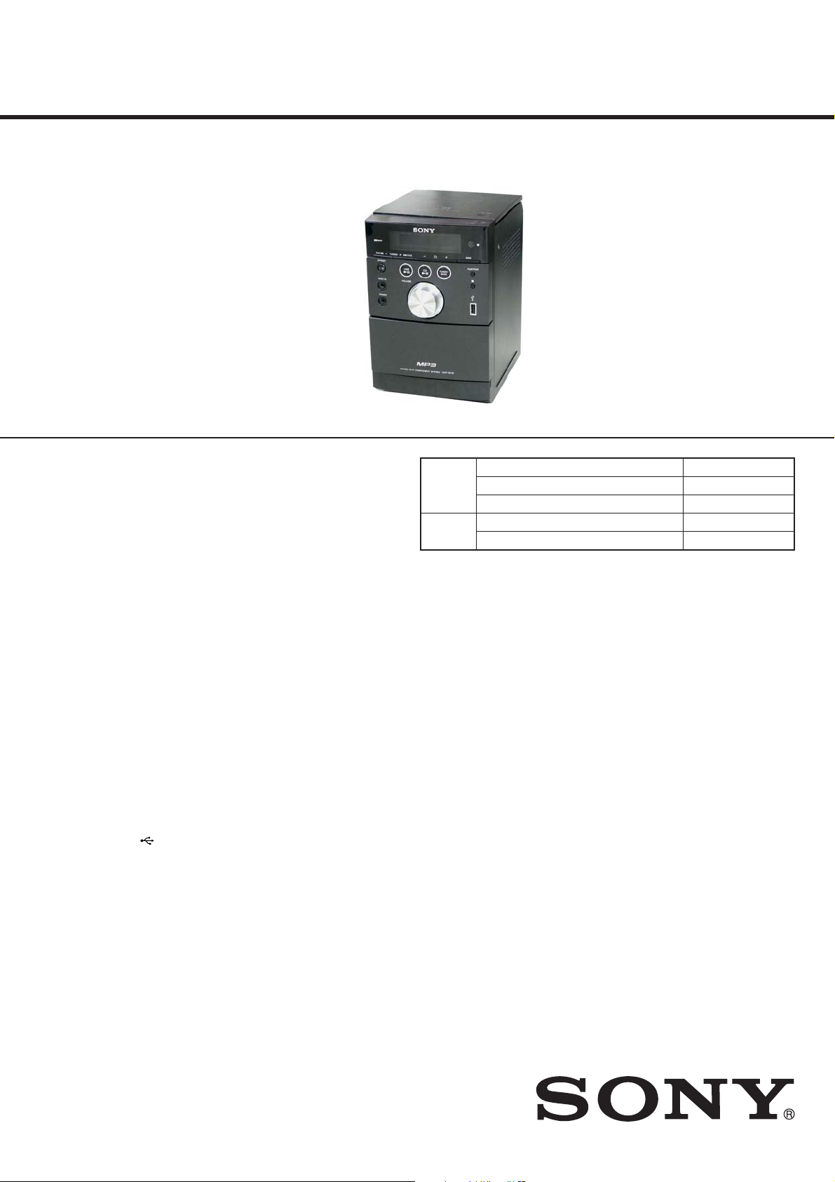
Photo: HCD-EH26
CD
Section
TAPE
Section
AEP Model
HCD-EH25/EH26
UK Model
Russian Model
Korean Model
HCD-EH25
Model Name Using Similar Mechanism NEW
Base Unit Name BU-K8BD90-WOD
Optical Pick-up Name KSM-213CDP
Model Name Using Similar Mechanism HCD-EH10
Tape Transport Mechanism T ype MF-EH10
Amplifier section
European and Russian models:
DIN power output (rated):
4 + 4 watts (4 ohms at 1 kHz, DIN)
Continuous RMS power output
(reference): 5 + 5 watts (4 ohms at
1 kHz, 10% THD)
Music power output (reference):
7 + 7 watts (4 ohms at 1 kHz, 10%
THD)
Other models:
DIN power output (rated):
4 + 4 watts (4 ohms at 1 kHz, DIN)
Continuous RMS power output
(reference): 5 + 5 watts (4 ohms at
1 kHz, 10% THD)
Inputs:
AUDIO IN (stereo mini jack):
voltage 800 mV, impedance
47 kilohms
(USB) port: Type A, maximum
current 500 mA
Outputs:
PHONES (stereo mini jack): accepts
headphones of 8 ohms or more
SPEAKER: accepts impedance of
4 ohms
SPECIFICATIONS
USB section
Supported bit rate
MP3 (MPEG 1 Audio Layer-3):
32 – 320kbps, VBR
Sampling frequencies
MP3 (MPEG 1 Audio Layer-3):
32/44.1/48 kHz
CD player section
System: Compact disc and digital audio
system
Laser Diode Properties
Emission Duration: Continuous
Laser Output*: Less than 44.6µW
* is output is the value measurement
at a distance of 200mm from the
objective lens surface on the Optical
Pick-up Block with 7mm aperture.
Frequency response: 20 Hz – 20 kHz
Signal-to-noise ratio: More than 90 dB
Dynamic range: More than 90 dB
Tape deck section
Recording system: 4-track 2-channel, stereo
Tuner section
FM stereo, FM/AM superheterodyne tuner
FM tuner section:
Tuning range:
87.5 − 108.0 MHz (50 kHz step)
Antenna: FM lead antenna
Intermediate frequency: 10.7 MHz
AM tuner section:
Tuning range
Korean model:
531 − 1,602 kHz (with 9 kHz tuning
interval)
530 − 1,610 kHz (with 10 kHz tuning
interval)
Other models:
531 − 1,602 kHz (9 kHz step)
Antenna: AM loop antenna
Intermediate frequency: 450 kHz
General
Power requirements
Korean model: 220 V AC, 60 Hz
Other models: 230 V AC, 50/60 Hz
Power consumption: 27 watts
Dimensions (w/h/d) (excl. speakers):
Approx. 155 × 241 × 224.6 mm
Mass (excl. speakers): Approx. 2.2 kg
Design and specications are subject to
change without notice.
9-889-152-01
2008E05-1
2008.05
©
COMPACT DISC DECK RECEIVER
Sony Corporation
Audio Business Group
Published by Sony Techno Create Corporation
Page 2

HCD-EH25/EH26
NOTES ON CHIP COMPONENT REPLACEMENT
• Never reuse a disconnected chip component.
• Notice that the minus side of a tantalum capacitor may be damaged by heat.
CAUTION
Use of controls or adjustments or performance of procedures
other than those specifi ed herein may result in hazardous radia-
tion exposure.
This appliance is classifi ed as
a CLASS 1 LASER product.
This marking is located on the
rear exterior.
TABLE OF CONTENTS
1. SERVICING NOTES ............................................. 3
2. GENERAL .................................................................. 4
3. DISASSEMBLY
3-1. Disassembly Flow ........................................................... 5
3-2. Rear Cabinet Block ......................................................... 5
3-3. Front Cabinet Block, Top Cabinet Block,
MAIN Board ................................................................... 6
3-4. MF-EH10 (Tape Mechanism Deck), Cassette Lid .......... 6
3-5. Base Unit Block (BU-K8BD90-WOD) .......................... 7
3-6. Optical Pick-up Block (KSM-213CDP) ......................... 7
4. TEST MODE ............................................................ 8
5. MECHANICAL ADJUSTMENTS ...................... 9
6. ELECTRICAL ADJUSTMENTS ........................ 9
7. DIAGRAMS
7-1. Block Diagram - CD SERVO Section - .......................... 12
7-2. Block Diagram - TUNER/USB Section - ....................... 13
7-3. Block Diagram - MAIN/POWER SUPPLY Section - .... 14
7-4. Printed Wiring Board - CD Board - ................................ 16
7-5. Schematic Diagram - CD Board - ................................... 17
7-6. Printed Wiring Board - USB Board - .............................. 18
7-7. Schematic Diagram - USB Board - ................................. 19
7-8. Printed Wiring Board - MAIN Board - ........................... 20
7-9. Schematic Diagram - MAIN Board (1/3) - ..................... 21
7-10. Schematic Diagram - MAIN Board (2/3) - ..................... 22
7-11. Schematic Diagram - MAIN Board (3/3) - ..................... 23
7-12. Printed Wiring Board - PANEL Board - ......................... 24
7-13. Schematic Diagram - PANEL Board - ............................ 25
7-14. Printed Wiring Board - PT-VBUS Board - ..................... 26
7-15. Schematic Diagram - PT-VBUS Board - ........................ 26
SAFETY-RELATED COMPONET WARNING!
COMPONENTS IDENTIFIED BY MARK 0 OR DOTTED LINE
WITH MARK 0 ON THE SCHEMATIC DIAGRAMS AND IN
THE PARTS LIST ARE CRITICAL TO SAFE OPERATION.
REPLACE THESE COMPONENTS WITH SONY PARTS
WHOSE PART NUMBERS APPEAR AS SHOWN IN THIS
MANUAL OR IN SUPPLEMENTS PUBLISHED BY SONY.
8. EXPLODED VIEWS
8-1. Overall Section ............................................................... 27
8-2. Front Cabinet Section ..................................................... 28
8-3. Top Cabinet Section ........................................................ 29
8-4. Base Unit Section (BU-K8BD90-WOD) ........................ 30
9. ELECTRICAL PARTS LIST .............................. 43
Accessories are given in the last of the electrical parts list.
2
Page 3
SECTION 1
SERVICING NOTES
HCD-EH25/EH26
NOTES ON HANDLING THE OPTICAL PICK-UP
BLOCK OR BASE UNIT
The laser diode in the optical pick-up block may suffer electrostatic break-down because of the potential difference generated by the
charged electrostatic load, etc. on clothing and the human body.
During repair, pay attention to electrostatic break-down and also
use the procedure in the printed matter which is included in the
repair parts.
The fl exible board is easily damaged and should be handled with
care.
NOTES ON LASER DIODE EMISSION CHECK
The laser beam on this model is concentrated so as to be focused
on the disc refl ective surface by the objective lens in the optical
pickup block. Therefore, when checking the laser diode emission,
observe from more than 30 cm away from the objective lens.
UNLEADED SOLDER
Boards requiring use of unleaded solder are printed with the leadfree mark (LF) indicating the solder contains no lead.
(Caution: Some printed circuit boards may not come printed with
the lead free mark due to their particular size)
: LEAD FREE MARK
Unleaded solder has the following characteristics.
• Unleaded solder melts at a temperature about 40 °C higher
than ordinary solder.
Ordinary soldering irons can be used but the iron tip has to be
applied to the solder joint for a slightly longer time.
Soldering irons using a temperature regulator should be set to
about 350 °C.
Caution: The printed pattern (copper foil) may peel away if
the heated tip is applied for too long, so be careful!
• Strong viscosity
Unleaded solder is more viscous (sticky, less prone to fl ow)
than ordinary solder so use caution not to let solder bridges
occur such as on IC pins, etc.
• Usable with ordinary solder
It is best to use only unleaded solder but unleaded solder may
also be added to ordinary solder.
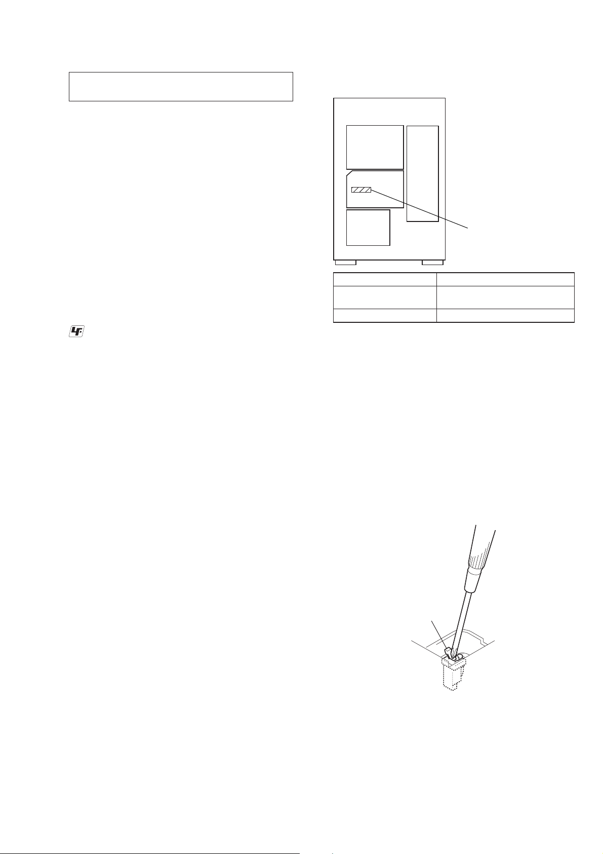
MODEL IDENTIFICATION
– Rear Cabinet –
Power Voltage
Indication
Model POWER VOLTAGE INDICATION
AEP, UK and Russian
models
Korean model AC 220 V, 60 Hz
LASER DIODE AND FOCUS SEARCH OPERATION
CHECK
During normal operation of the equipment, emission of the laser
diode is prohibited unless the upper lid is closed while turning on
the SW750. (push switch type)
The following checking method for the laser diode is operable.
• Method
Emission of the laser diode is visually checked.
1. Open the upper lid.
2. Push the SW750 as shown in Fig.1.
Note: Do not push the detection lever strongly , or it may be bent or dam-
aged.
3. Check the object lens for confi rming normal emission of the
laser diode. If not enitting, there is a trouble in the automatic
power control cirsuit or the optical pick-up.
In this operation, the object lens will move up and down 2
times along with inward motion for the focus search.
AC 230 V, 50/60 Hz
SW750
Fig.1 Method to push the SW750
3
Page 4
HCD-EH25/EH26
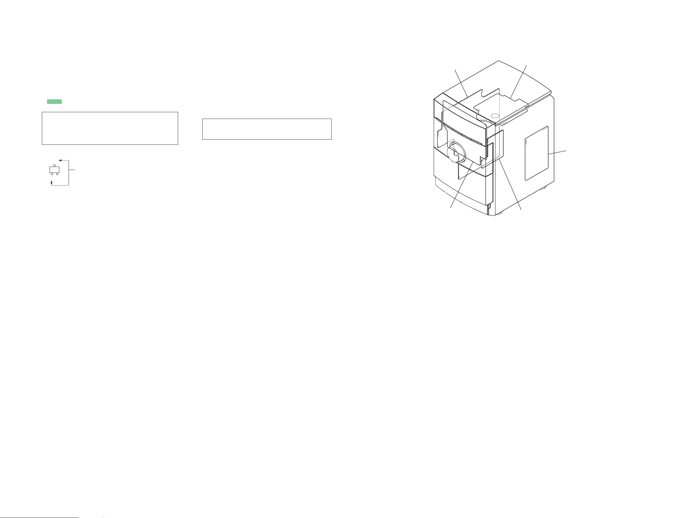
SECTION 2
GENERAL
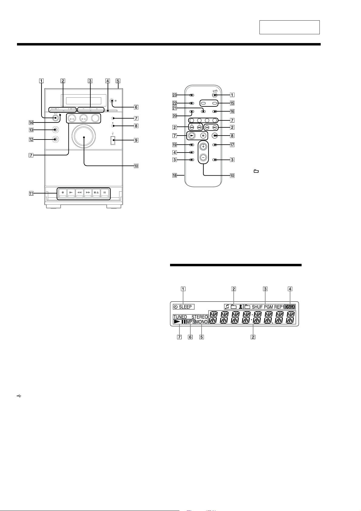
Guide to parts and controls
is manual mainly explains operations using the remote, but the same operations can
also be performed using the buttons on the unit having the same or similar names.
This section is extracted
from instruction manual.
Unit
Remote sensor
Playback buttons and function
buttons
Unit: USB (play/pause)
button
Press to select the USB function.
Presstostartorpauseplaybackofan
optional USB device.
Remote: USB button
Press to select the USB function.
Unit: CD (play/pause)
button
Press to select the CD function.
Press to start or pause playback of a disc.
Remote: CD button
Press to select the CD function.
Remote: (play) button,
(pause) button
Press to start or pause playback.
TUNER/BAND button
Press to select the TUNER function.
Press to select FM or AM reception
mode.
FUNCTION button
Press to select the function.
(stop) button
Press to stop playback.
(USB) port
Connect to an optional USB device.
R
Unit: VOLUME control
Remote: VOLUME +/− button
Turn or press to adjust the volume.
RB
(record) button, (play)
button, / (rewind/fast
forward) button, (stop/
eject) button, (pause) button
Press to operate the tape functions.
RT
PHONES jack
Connect the headphones.
RE
AUDIO IN jack
Connect to an optional audio
component.
RG
STANDBY indicator
Lights up when the system is turned o.
RH
CLOCK/TIMER SELECT button
CLOCK/TIMER SET button
Press to set the clock and the Play Timer.
RI
REPEAT/FM MODE button
Press to listen to a disc or USB device
repeatedly. Or press to listen to a single
track/le or all tracks/le in a folder (for
USB devices only) repeatedly.
Press to select the FM reception mode
(monaural or stereo).
RK
ENTER button
Press to enter the settings.
RL
Battery compartment lid
RM
CLEAR button
Press to delete a pre-programmed track
le.
X
TUNER MEMORY button
Press to preset the radio station.
XB
PLAY MODE/TUNING MODE
button
Press to select the play mode of a CD or
MP3 disc.
Press to select the tuning mode.
XT
DISPLAY button
Presstochangethe informationonthe
display.
XE
SLEEP button
Press to set the Sleep Timer.
Remote
Information on the display
Timer
Text information
Play mode
DSGX
Tuner reception mode
Tuner reception
Audio format
Play/Pause
/ (power) button
Press to turn on the system.
/ (go back/go forward)
button
Press to select a track or le.
Unit: TUNING +/− (tuning)
button
Remote: +/− (tuning) button
Press to tune in the desired station.
/ (rewind/fast forward)
button
Press to nd a point in a track or le.
+/− (select folder) button
Press to select a folder.
Sound buttons
Unit: DSGX button
Remote: EQ button
Press to select the sound eect.
PUSH OPEN/CLOSE
Press to open or close the CD
compartment.
4
Page 5
DISASSEMBLY
• This set can be disassembled in the order shown below.
3-1. DISASSEMBLY FLOW
SET
3-2. REAR CABINET BLOCK
(Page 5)
3-3. FRONT CABINET BLOCK,
TOP CABINET BLOCK,
MAIN BOARD
(Page 6)
HCD-EH25/EH26
SECTION 3
3-4. MF-EH10 (TAPE MECHANISM DECK),
CASSETTE LID
(Page 6)
Note: Follow the disassembly procedure in the numerical order given.
3-2. REAR CABINET BLOCK
screw
(KTP2 3 × 8)
3-5. BASE UNIT BLOCK
(BU-K8BD90-WOD)
(Page 7)
3-6. OPTICAL PICK-UP BLOCK
(KSM-213CDP)
(Page 7)
(BVTP3 × 10)
two screws
(BVTP3 × 10)
screw
(KTP2 3 × 8)
two screws
connector
(CN002)
connector
(CN103)
two screws
(BVTP3 × 10)
rear cabinet block
5
Page 6
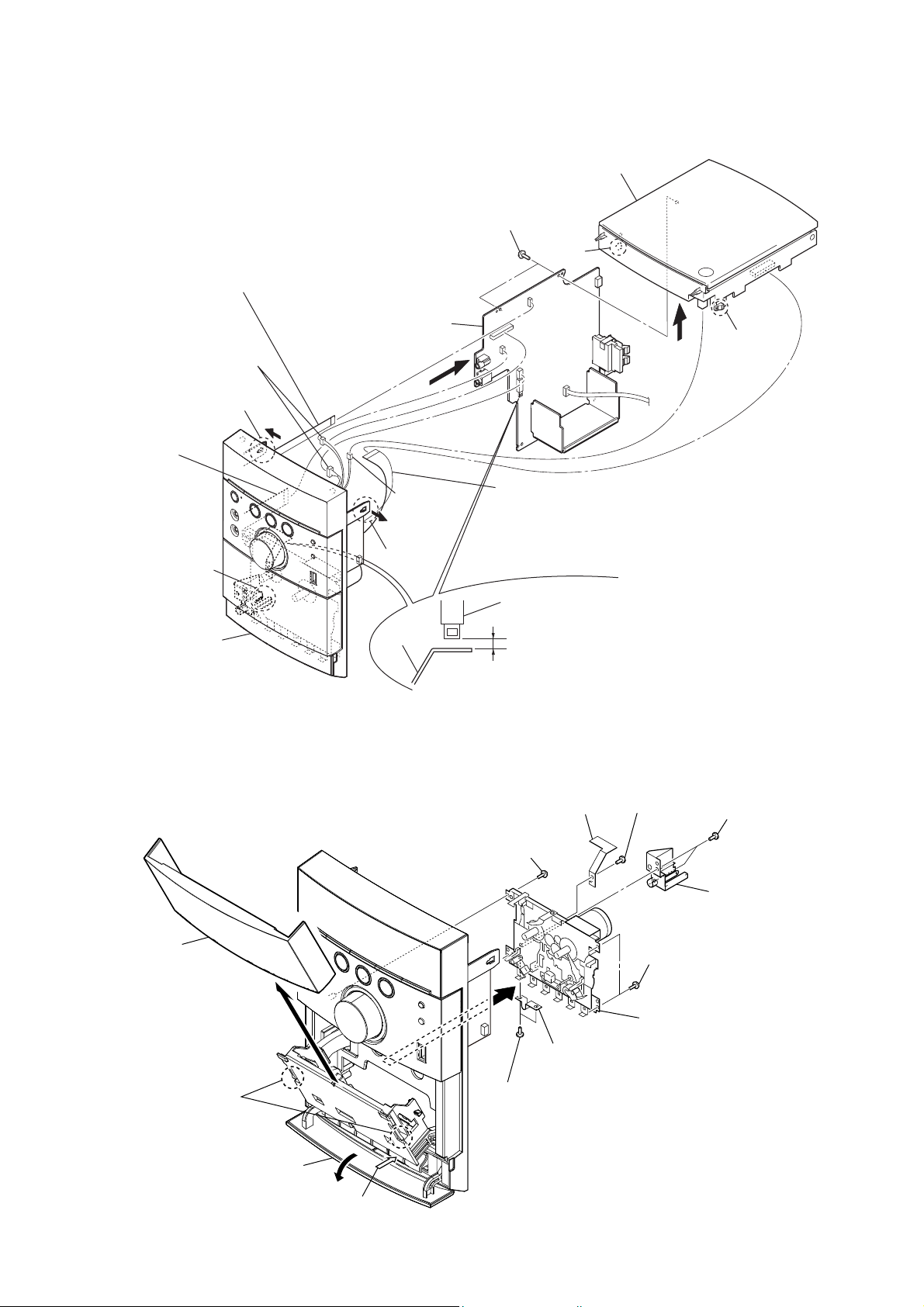
HCD-EH25/EH26
3-3. FRONT CABINET BLOCK, TOP CABINET BLOCK, MAIN BOARD
top cabinet block
R
two screws
(Russian, Korean models),
flexible flat cable (7 core) (FFC001)
(AEP, UK models)
(CN106)
two connectors
(CNP501, CNP502)
flexible flat cable (17 core)
(FFC002) (CN105)
flexible flat cable (5 core) (FFC001)
MAIN board
RB
claw
(BVTP2.6)
claw
claw
connector
(SW750)
claw
front cabinet block
claw
REC lever
Note: Adjust so that the space of slide switch (REC/PB) (SW501)
3-4. MF-EH10 (TAPE MECHANISM DECK), CASSETTE LID
screw
(BVTP2.6)
flexible flat cable (FFC003)
(CN201)
slide switch (REC/PB) (SW501)
2.3 ± 0.4 mm
REC lever becames 2.3 ± 0.4 mm
screw
lever (REC)
.
two screws
(BVTP2.6)
PWB holder
cassette lid
RE
Note: When removing cassette lid,
it's possible to remove cassette
lid by the order of RT RE.
two claws
RT
Open the button cover (C).
6
Push the eject button.
two screws
cable holder
R
two screws
(BVTP2.6)
MF-EH10
RB
(tape mechanism deck)
Page 7
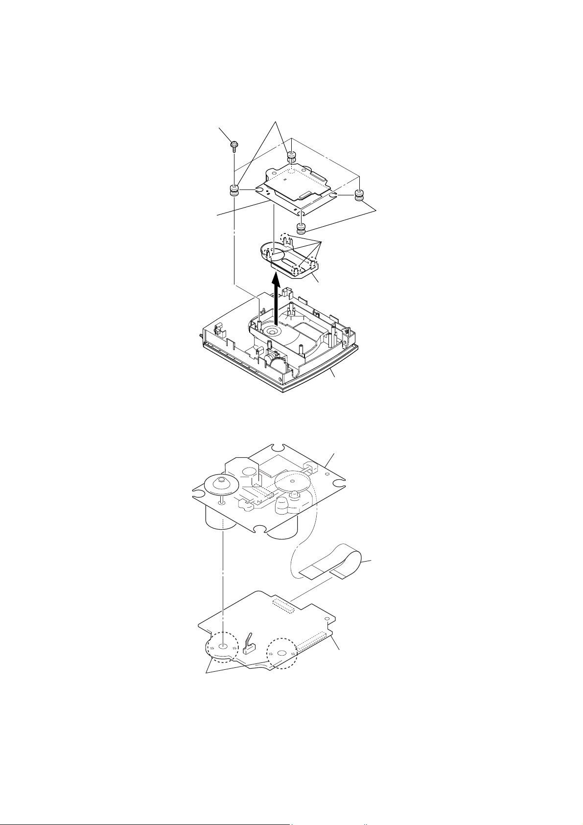
3-5. BASE UNIT BLOCK (BU-K8BD90-WOD)
Note: This illustration sees the top cabinet block back side from back.
HCD-EH25/EH26
four screws
(PWH B2.6)
base unit block
(BU-K8BD90-WOD)
two vibration proof rubbers
(green)
CD cover
(red)
four claws
top cabinet block
– Bottom view –
two vibration proof rubbers
3-6. OPTICAL PICK-UP BLOCK (KSM-213CDP)
Remove the four solders.
optical pick-up block
(KSM-213CDP)
wire (flat type) (16 core)
(optical pick-up, CD board: CN301)
CD board
7
Page 8

HCD-EH25/EH26
SECTION 4
TEST MODE
COLD RESET
The cold reset clears all data including preset data stored in the
memory to initial conditions. Execute this mode when returning
the set to the customer.
Procedure:
1. Press three buttons of [x], [l
. –
TUNING] and [
?/1
simultaneously.
2. When “RESET” appears, the set enters standby status.
PANEL TEST MODE
Procedure:
1. Press the [
2. Press three buttons of [FUNCTION], [USB], and [
] button to turn the power on.
?/1
?/1
] simul-
taneously.
3. When the panel test is activated, [STANDBY] LED and segments on the liquid crystal display are all turned on.
4. Press the [CD
u] button, date and version are displayed. For
example, “0403V101”.
5. Press the [TUNER/BAND] button, model name and destination are displayed. For example, “EH25CE2”.
6. To release from this mode, press three buttons of [FUNC
TION], [USB], and [
] simultaneously.
?/1
TUNER STEP CHANGE
(EH25: Korean)
The AM tuning interval can be changed over 9 kHz or 10 kHz.
Procedure:
1. Press the [
] button to turn the power on.
?/1
2. Press the [TUNER/BAND] button to select TUNER (AM)
function.
3. Press the [
] button again to turn the power off (standby).
?/1
4. After pressing the [DISPLAY] button on the remote commander, while pressing the [TUNING + M L] button, press the
[
] button.
?/1
5. It turns power on and display “9K STEP” or “10K STEP”, and
thus the tuning interval is changed over.
CD SERVICE MODE
This mode can move the SLED of the optical pick-up, and also can
turn the optical pick-up laser power on and off.
Procedure:
1. Press the [
] button to turn the power on.
?/1
2. Press the [FUNCTION] button to select CD function.
3. Press three buttons of [l m – TUNING], [FUNCTION],
and [
] simultaneously.
?/1
4. It enters the CD service mode and displays “SERVICE”.
5. To release from this mode, press three buttons of [l m
– TUNING], [FUNCTION] and [
] simultaneously.
?/1
Key Operation:
[TUNING + M L], [l m – TUNING]:
Use these keys to move the SLED. When [TUNING + M
L] is pressed in this mode, the SLED moves to outer cir-
cumference and the message “SLED OUT” is displayed.
When [
l m – TUNING] is pressed in this mode, the
SLED moves to inner circumference and the message
“SLED IN” is displayed.
CD ERROR CODE
The past errors of the optical pick-up system (= optical unit + CD
board) are displayed as the BD Errors as shown below.
Procedure:
1. Press the [
]
2. Press the [FUNCTION] button to select CD function.
] button to turn the power on.
?/1
3. Press three buttons of [l m – TUNING], [DSGX] and
[
] simultaneously.
?/1
4. Then, the BD error code is displayed as “D0xxxxxx” (x means
hexadecimal number) on the liquid crystal display as shown
below.
5. Every pressing of the [TUNING +
M L] button in this
mode increments the number after “D” starting from “D0” up
to “D4”, and then returns to “D0”. Every pressing of the [
m – TUNING] button in this mode decrements the number
after “D”. The smaller the error code number is, the newer the
error content is.
6. To release from this mode, press the [
] button to turn the
?/1
power off.
Contents of “BD Errors”
Error display example
D 0 01 06 01
1 2 3 4
1 It indicates the error history number
0 to 4: The error code number 0 indicates the newest error.
2 It indicates the error content
01: The focus servo cannot lock-in.
02: GFS is no good (NG).
03: The startup time exceeds the specifi ed period of time
(time over)
04: The focus servo is unlocked continuously.
05: Q code cannot be obtained within the specifi ed period of
time.
06: The tracking servo cannot lock-in.
07: Blank disc
3 It indicates the on-going processing of optical pick-up system
(= optical unit + CD board) when the trouble has occurred.
01: The CD SHIP mode processing is in progress.
02: The POWER OFF processing is in progress.
03: The POWER ON processing is in progress.
04: The INITIALIZE processing is in progress.
05: The optical pick-up system (= optical unit + CD board)
is in the stop state.
06: The STOP operation is in progress.
07: The startup processing is in progress.
08: The TOC read-in processing is in progress.
09: The SEARCH operation is in progress.
0A: The PLAY operation is in progress.
0B: The PAUSE operation is in progress.
0C: The PLAY – MANUAL SEARCH operation is in prog-
ress.
0D: The PAUSE – MANUAL SEARCH operation is in prog-
ress.
l
[FUNCTION]:
Use this key to turn the optical pick-up laser power on and
off. When the laser power is turned on, the message “LD
ON” is displayed. When the laser power is turned off, the
message “LD OFF” is displayed.
8
4 It indicates the operation that is being processed when the trou-
ble has occurred.
It indicates the step number of each processing specifi ed by 3.
Because the numbers of steps are different in each processing,
this number is different in each processing.
Page 9
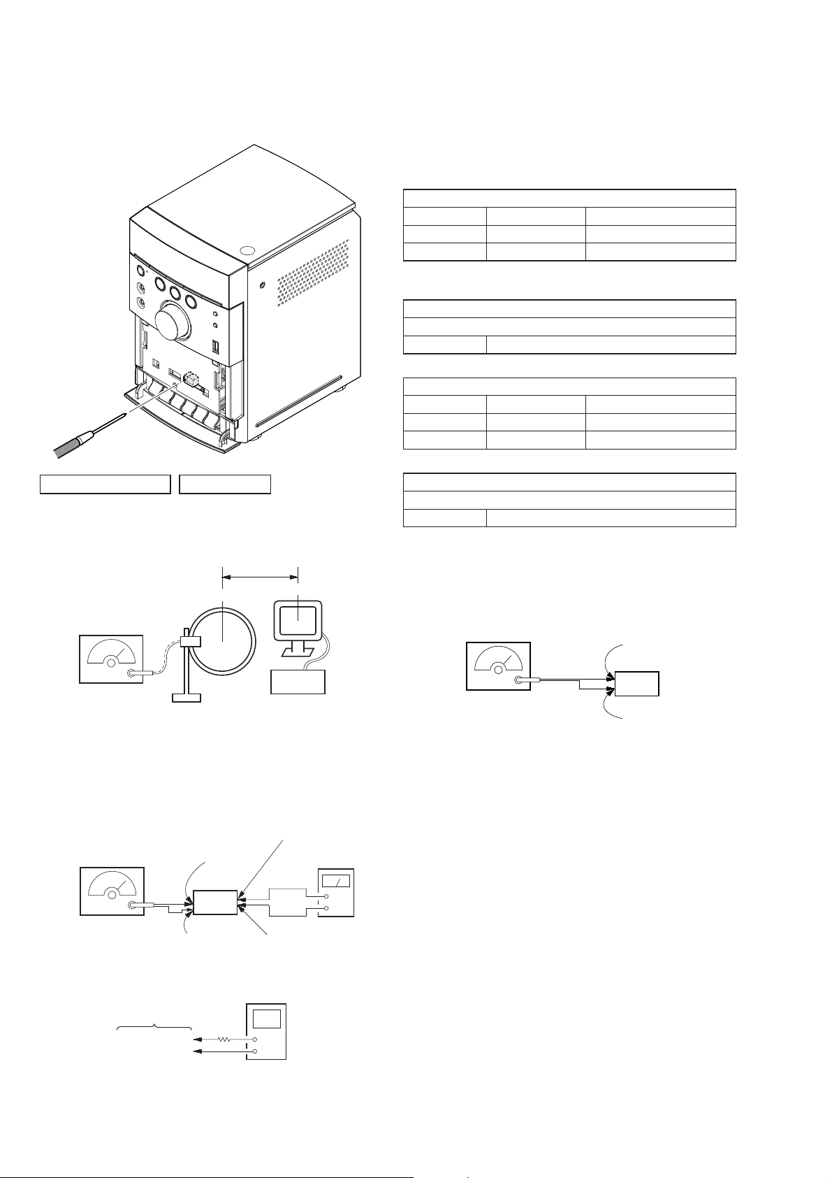
SECTION 5
MECHANICAL ADJUSTMENTS
HCD-EH25/EH26
SECTION 6
ELECTRICAL ADJUSTMENTS
Precaution
1. Clean the following parts with a denatured-alcohol-moistened
swab:
record/playback head pinch roller
erase head rubber belts
capstan idlers
2. Demagnetize the record/playback head with a head demagnetizer. (Do not bring the head magnetizer close to the erase
head.)
3. Do not use a magnetized screwdriver for the adjustments.
4. After the adjustments, appiy suitable locking compound to the
parts adjusted.
5. The adjustments should be performed with the rated power
supply voltage unless otherwise noted.
Torque Measurement
Mode Torque meter Meter reading
FWD CQ-102AS
FWD
Back Tension
FF CQ-201AS
REW CQ-201B
CQ-102C
2.0 – 8.0 mN • m
(20 – 80 g • cm)
(0.28 – 1.12 oz • inch)
0.15 – 0.6 mN • m
(1.5 – 6.0 g • cm)
(0.021 – 0.083 oz • inch)
5.0 – 17.7 mN • m
(50 – 177 g • cm)
(0.7 – 2.48 oz • inch)
5.0 – 17.7 mN • m
(50 – 177 g • cm)
(0.7 – 2.48 oz • inch)
Tape Tension Measurement
Mode Torque meter Meter reading
FWD CQ-403A
more than 80 g
(more than 2.82 oz)
DECK SECTION 0 dB = 0.775
1. Demagnetize the record/playback head with a head
demagnetizer.
2. Do not use a magnetized screwdriver for the adjustments.
TEST TAPE
Tape Signal Used for
P-4-A063 6.3 kHz, –10 dB Azimuth Adjustment
RECORD/PLAYBACK HEAD AZIMUTH ADJUSTMENT
Procedure:
1. Mode: Playback
test tape
P-4-A063
(6.3 kHz, –10 dB)
2. Turn the adjustment screw and check output peaks. If the peaks
do not match for L-CH and R-CH, turn the adjustment screw
so that outputs match within 1dB of peak.
L-CH
peak
Output
level
R-CH
Screw
position
peak
set
within
1 dB
L-CH
peak
MAIN board
PHONES jack
(J102)
R-CH
peak
level meter
+
–
within
1 dB
Screw
position
3. Mode: Playback
test tape
P-4-A063
(6.3 kHz, –10 dB)
in phase 45° 90° 135° 180°
MAIN board
PHONES jack
(J102)
set
waveform of oscilloscope
good
oscilloscope
V
wrong
H
4. Confi rm that oscilloscope waveform is clear and check RF sig-
nal level is correct or not.
9
Page 10
HCD-EH25/EH26
Adjustment Location: Record/Playback/Erase Head
Note: Remove the cassette lid before this adjustment.
Refer to “DISASSEMBLY” (page 5)
TUNER SECTION
0 dB = 1 μV
[AM]
Setting:
Function: TUNER
Band: AM
60 cm
loop antenna A
AM RF signal
generator
30% amplitude
modulation by
400 Hz signal
loop antenna B
set
[FM]
Setting:
Function: TUNER
Band: FM
MAIN board
JW403
FM RF signal
generator
MAIN board
CNP802 pin
(TUNER OUT L-ch)
level meter
• Repeat the procedures in each adjustment several times, and
the tracking adjustments should be fi nally done by the trimmer
capacitors.
• Remove FM antenna in FM adjustment.
( ): AEP, Russian and UK models
AM VT VOLTAGE ADJUSTMENT
Adjustment Part Frequency Display Reading on Digital Voltmeter
L852 530 (531) kHz 1.5 ± 0.1 V
Confi rmation 1710 (1602) kHz 8.0 (7.2) ± 0.5 V
( ): AEP, Russian and UK models
AM TRACKING ADJUSTMENT
Adjust for a maximum reading on level meter
L851 530 (531) kHz
FM VT VOLTAGE ADJUSTMENT
Adjustment Part Frequency Display Reading on Digital Voltmeter
L805 87.5 MHz 1.75 ± 0.1 V
Confi rmation 108 MHz 6.2 ± 0.5 V
FM TRACKING ADJUSTMENT
Adjust for a maximum reading on level meter
L804 98 MHz
FM DETECTOR ADJUSTMENT
Setting:
Function: TUNER
BAND button: FM
FM RF Signal
generator
Carrier frequency : 98 MHz
Modulation : deviation by
FM 75 kHZ
Output level : 60 dB
MAIN board
JW403
(TUNER OUT L-ch)
set
MAIN board
JW148 (GND)
1. Tune the set to 98 MHz.
2. Adjust L806 so that modulation distortion may become the
best in the vicinity of the maximum value where the tuner out
level becomes -156Bs or more.
1 kHz frequency
deviation by FM 75 kHz
signal
Output level:
as low as possible
JW821 (VT)
JW805 (GND)
10
MAIN board
CNP802 pin
MAIN board
set
digital voltmeter
10 kΩ
+
–
MAIN board
JW148
(GND)
Page 11
HCD-EH25/EH26
V
Adjustment Location:
– MAIN Board (Component Side) –
L805
FM VT
Voltage
Adjustment
L806
FM Detector
Adjustment
L804
FM Tracking
Adjustment
– MAIN Board (Conductor Side) –
CNP802
JW805
(GND)
1
3
L852
AM VT
Voltage
Adjustment
L851
AM Tracking
Adjustment
JW403
(TUNER OUT L-ch)
CD SECTION
Note:
1. CD Block is basically constructed to operate without adjustment.
2. Use YEDS-18 disc (3-702-101-01) unless otherwise indicated.
3. Use an oscilloscope with more than 10 MΩ impedance.
4. Clean the object lens by an applicator with neutral detergent when the
signal level is low than specifi ed value with the following checks.
5. Check the focus bias check when optical pick-up block is replaced.
FOCUS BIAS CHECK
oscilloscope
(DC range)
CD board
TP122 (RFEQO)
TP124 (VC)
Procedure:
1. Connect oscilloscope to TP122 (RFEQO) and TP124 (VC) on
the CD board.
2. Press the [
] button to turn the power on.
?/1
3. Set the disc (YEDS-18) and press the [CD u] button to playback.
4. Confi rm that oscilloscope waveform is as shown in the fi gure
below. (eye pattern)
A good eye pattern means that the diamond shape (◊) in the
center of the waveform can be clearly distinguished.
+
–
VOLT/DIV: 200 m
TIME/DIV: 500 ns
JW821
(VT)
JW148
(GND)
JW402
(TUNER OUT R-ch)
FM TUNE LEVEL CHECK
signal
generator
set
Procedure:
1. Turn on the set.
2. Input the following signal from signal generator to FM antenna
input directly.
Carrier frequency : A = 87.5 MHz, B = 98 MHz, C = 108 MHz
Deviation : 75 kHz
Modulation : 1 kHz
ANT input : 35 dBu (EMF)
Note: Use 75 ohm coaxial cable to connect signal generator and the set.
You cannot use video cable for checking.
Use signal generator whose output impedance is 75 ohm.
Checking Location:
– CD Board (Conductor Side) –
TP124
(VC)
TP122
(RFEQO)
level:
1.2 ± 0.3 Vp-p
IC101
3. Set to FM tuner function and tune A, B and C signals.
4. Confi rm “TUNED” is lit on the display for A, B and C sig-
nals.
When the selected station signal is received in good condition,
“TUNED” is displayed.
11
Page 12
HCD-EH25/EH26
SECTION 7
DIAGRAMS
7-1. BLOCK DIAGRAM - CD SERVO Section -
AVDD
DETECTOR
A
B
C
D
E
F
LASER DIODE
PD
LD
I-V AMP
VCC
+3.3V
A
B
C
D
E
F
AUTOMATIC
LD
PD
POWER
CONTROL
Q301
FNi1 (A)
95
97 FPi1 (B)
94 FNi2 (C)
96 FPi2 (D)
100 TNi (E)
98 TPi (F)
91 LDo 92MDi
RFo
89
3RFRP RFZI
88
2
76TEi TEZi
AGCi
83RFEQo 81 RFi
82 RFRPi
30LO
27RO
R-CH
CD-L
(Page 14)
A
OPTICAL PICK-UP
BLOCK
(KSM-213DCP)
M401
(SPINDLE)
M402
(SLED)
2-AXIS
DEVICE
(TRACKING)(FOCUS)
VC
SP+
M
SP–
SL+
M
SL–
T+
T–
F+
F–
R-ch is omitted due to same as L-ch.
SIGNAL PATH
: CD PLAY
FOCUS/TRACKING COIL DRIVE,
SLED/SPINDLE MOTOR DRIVE
IC401
BIAS 23
2VO1+
3
IN1
1VO1–
12 VO2–
IN2’ 9
11 VO2+
18 VO3+
17 VO3–
26 VO4+
27
VO4–
MUTE
7
IN3’
IN4’
DVDD
+3.3V
20
24
S201
(LIMIT)
84 VRo
13 DMo
12 FMo
10 TRO
9FMO
20 IO0 (/HSO)
CD-MP3 PROCESSOR
IC101
SYSTEM CONTROLLER
IC701 (1/3)
38BUS0
39BUS1 6BUS1
40BUS2 (SO) 7BUS2
41BUS3 (SI) 8BUS3
42BUCK (CLK)
43XCCE
48PIO0
5BUS0
10 BUCK
11 XCCEN
3REQ
12
XI
23
X102
16.9344MHz
54SBSY
37XRST
XO
24
43 SBSY
12 XRST
4 MMUT
Page 13
HCD-EH25/EH26
HCD-EH25/EH26
1313
7-2. BLOCK DIAGRAM - TUNER/USB Section -
FM MIX
AMP
Q803
FM/AM TUNER,
FM/AM PLL
IC801
RDS DECODER
IC861
36
FMRF-IN
8
FMIF-IN
22
MPX-IN
1
AMRF-IN
31
AM-OSC
25
TU_DO
56
TU_CLK
55
TU_CE
57
TU_DI
39
TU_ASD
SYSTEM CONTROLLER
IC701 (2/3)
+4V
REGULATOR
Q862
VM +9V RDS +4V
X801
75kHz
2019
XIN
XOUT
16DI17CL15
CE
18
DO25AGC
1
CNP802
ANTENNA
FM/AM
3
BAND-PASS
FILTER
BPF801
AM
TRACKING
L851
AM-RF
AM VT
VOLTAGE
L852
AM-OSC
D851
CF801
7
AMIF-IN
L803
AM-IFT
34
FMRF-OUT
FM
TRACKING
L804
FM-RF
32
FM-OSC
FM VT
VOLTAGE
L805
FM-OSC
VM +9V
11
FM-DET
FM
DETECTOR
L806
FM-DET
3
FM-MIX
30BO2
23
FMDET-OUT
12
L-OUT
13
R-OUT R-CH
TUNER-L
5
AM-MIX
24
AMDET-OUT
CF802
CF803
4
FIN
DET AMP
Q861
26
RDS_DATA
2
D0
45
RDS_CLK
16
CL
X861
4.332MHz
1413
XIN
XOUT
B
• SIGNAL PATH
: AM
• R-ch is omitted due to same as L-ch.
: FM
(EH25: AEP, UK/EH26)
3
CN104
(USB)
D+
D–
2
USB CONTROLLER
IC101
D/A CONVERTER
IC105
USB_DP34
USB_DM
33
DATA
55
LRCK
53
BCK
54
DIN1
LRCI
3
MCLK
2
VOUTL 8
VOUTR
5
XOUT_PLL
XIN_PLL
40 41
X101
16.9344MHz
CLOCK SHIFT
IC104
MCLK
4
RESETX
1
SDA
13
SCL
12
BUSY
11
MCHNG
10
USB_SDA
49
USB_SCL
50
USB_BUSY
19
MCHING
18
USB_RESET
17
: USB
R-CH
C
USB-L
(Page 14)
(Page 14)
Page 14
HCD-EH25/EH26
HCD-EH25/EH26
1414
7-3. BLOCK DIAGRAM - MAIN/POWER SUPPLY Section -
R-CH
INPUT SELECTOR,
ELECTRICAL VOLUME
IC401
28
REC1O
18
OUT1
13
SD
23
C1
21
B1
2
PB1P
19
A1
R-CH
CD-L
A
TUNER-L
• SIGNAL PATH
: CD PLAY
: TAPE PLAY
: REC
• R-ch is omitted due to same as L-ch.
J105
AUDIO IN
J102
PHONES
SPEAKER
+
–
–
+
R
L
J101
BIAS OSC
L501
OSC
Q507
TPR501
(REC/PB)
TAPE
MECHANISM
DECK
L-CH
SW501-1
SW501
(REC/PB)
PB
S
REC
R-CH
R-CH
POWER
AMP
IC301
33
FUNC_SDA
RMC
9
SYSTEM CONTROLLER
IC701 (3/3)
+
(AC IN)
F001
POWER
TRANSFORMER
PT005
SYS +3.3V
D702
D116 – 118
D372
AMP B+
RECT
D107 – 110
B+ SWITCH
Q351, 352
AC DETECT
Q371, 372
AC DETECT
Q121, 122
VOLTAGE
DETECT
Q705, 706
RECT
D111, 113
VSTBY
+9V
REGULATOR
Q101 – 103
VM +9V
USB
DVDD +3.3V
VM +7V
TUNER +5V
TUNER +3V
46POWER_ON
42HOLD
36P_MONI
54REST
REMOTE CONTROL
RECEIVER
IC703
LED DRIVE
Q707
LED701
(LCD BACK LIGHT)
LED_STBY
22
LED
1
LED702
X701
32768Hz
14 13
X3
X2
92 93
X702
5.53MHz
X1
X0
LCD702
LIQUID
CRYSTAL
DISPLAY
48 RE_VOL
2 CD OPEN/CLOSE
ROTARY
ENCODER
SW700
VOLUME
STANDBY
SW701 – 711
(FRONT PANEL KEYS)
SW750
(CD LID OPEN/CLOSE DETECT)
KEY1 – KEY3
37, 38, 41
COM0 – COM3
59 – 62
SEG0 – SEG31
63, 64, 67 – 89, 94 – 100
RESET
SWITCH
Q704
B
SW501-2
40
TP_STATE
DC
DETECT
Q123
LED DRIVE
Q711, 712
LINE FILTER
LF901
REGULATOR
Q701 – 703
REGULATOR
Q802
REGULATOR
Q801
+3.3V
REGULATOR
IC707
+3.5V
REGULATOR
IC706
D703
+1.5V
REGULATOR
IC201
+1.5V
REGULATOR
IC102
VOLTAGE
DETECTOR
IC709
Q710
D704, 705
B+ SWITCH
Q713, 714
USB AVDD +3.3V
USB +1.5V
AVDD +3.3V
DVDD +3.3V
VDD +1.5V
24USB_REG_ON
23CD_ON
RECT
D901, 902
+5V
REGULATOR
IC901
VBUS POWER
ON/OFF SWITCH
IC103
VBUS B+
AUDIO SELECT
SWITCH
IC451
USB-L
C
: USB
: AUDIO IN
: FM
30
AUDIO_SW
34
AMP_ON
21
USB_EN
20
USB_FLG
+
+3.3V
REGULATOR
Q708
+3.3V
REGULATOR
Q709
(Page 12)
(Page 13)
(Page 13)
Page 15
HCD-EH25/EH26
HCD-EH25/EH26
1515
For Schematic Diagrams.
Note:
• All capacitors are in μF unless otherwise noted. (p: pF) 50
WV or less are not indicated except for electrolytics and
tantalums.
• All resistors are in Ω and 1/4 W or less unless otherwise
specifi ed.
• f : internal component.
• C : panel designation.
THIS NOTE IS COMMON FOR PRINTED WIRING BOARDS AND SCHEMATIC DIAGRAMS.
(In addition to this, the necessary note is printed in each block.)
• A : B+ Line.
• H : adjustment for repair.
• Voltages and waveforms are dc with respect to ground
under no-signal (detuned) conditions.
– CD board –
no mark : CD PLAY
– USB board –
no mark : USB
– Other board –
no mark : FM
[ ] : AM
( ) : CD PLAY
‹‹ ›› : USB
< > : TAPE PLAY
{ } : REC
* : Impossible to measure
• Voltages are taken with VOM (Input impedance 10 MΩ).
Voltage variations may be noted due to normal production
tolerances.
• Waveforms are taken with a oscilloscope.
Voltage variations may be noted due to normal production
tolerances.
• Circled numbers refer to waveforms.
• Signal path.
F : FM
f : AM
J : CD PLAY
N : USB
E : TAPE PLAY
j : REC
h : AUDIO IN
• Abbreviation
KR : Korean model
RU : Russian
model
For Printed Wiring Boards.
Note:
• X : Parts extracted from the component side.
• Y : parts extracted from the conductor side.
• W : indicates side identifi ed with part number.
• f : internal component.
• : Pattern from the side which enables seeing.
(The other layers' patterns are not indicated.)
• Indication of transistor.
Note: The components identifi ed by mark 0 or dotted
line with mark 0 are critical for safety.
Replace only with part number specifi ed.
Caution:
Pattern face side:
(Conductor Side)
Parts face side:
(Component Side)
Parts on the pattern face side seen from
the pattern face are indicated.
Parts on the parts face side seen from
the parts face are indicated.
• Circuit Boards Location
C
Q
B
E
These are omitted.
MAIN board
PANEL board
CD board
PT-VBUS board
USB board
Page 16
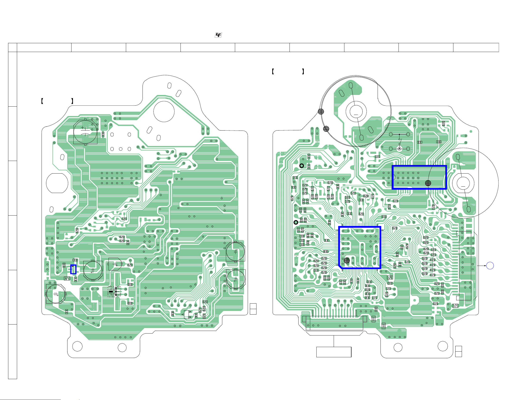
HCD-EH25/EH26
HCD-EH25/EH26
1616
• : Uses unleaded solder.
• See page 15 for Circuit Boards Location.
7-4. PRINTED WIRING BOARD - CD Board -
R150
R149
R148
R108
R154
R153
C148
C110
C109
C301
C303
C302
C104
R110
C116
C404
R203
R204
R205
R206
R207
R208
R209
R210
R219
R223
R222
R147
R221
R218
R146
R145
C150
R113
C403
R202
C151
C108
C105
C147
C146
C145
C152
C118
C117
C144
C101
C125
CN201
C143
C120
R144
R157
C142
C141
C140
C100
C107
R408
R156
C124
C127
C126
CN301
R101
C119
C102
R415
R414
C103
R405
C113
R102
R402
R105
R106
C132
C138
C137
R135
R134
R136
R130
R128
R129
R143
R139
C136
R120
R114
C153
C112
R125
R126
C149
C139
R127
R118
R140
R151
C122
C123
R220
R104
S201
R155
C128
C106
C201
R304
R302
C309
C205
C207
C307
R303
C133
R111
R112
C115
R211
Q301
R301
C204
C202
C206
C306
R212
C401
C130
C405
IC201
IC401
IC101
R201
R142
CD BOARD (COMPONENT SIDE)
CD BOARD (CONDUCTOR SIDE)
314
5
17 814
28 22 21 15
TP124
(VC)
TP122
(RFEQO)
1
25
26
50
5175
76
100
1
21
A
PANEL
BOARD
CNP701
161
1-872-135-
11
(11)
1-872-135-
11
(11)
OPTICAL PICK-UP BLOCK
(KSM-213CDP)
A
B
C
D
E
F
123456789
E
(LIMIT)
M401
(SPINDLE)
M402
(SLED)
M
M
X102
(Page 24)
Page 17
HCD-EH25/EH26
HCD-EH25/EH26
1717
• See page 23 for Waveforms. • See page 27 for IC Block Diagrams. • See page 33 for IC Pin Function Description.
7-5. SCHEMATIC DIAGRAM - CD Board -
R108
R154
R153
C201
R304
R201
R110
R303
R203
R204
R205
R206
R207
R208
R209
R210
R219
R223
R222
R221
R218
R112
R202
R211
Q301
R301
C202
R157
TP122 (RFEQO)
TP124 (VC)
R156
CN301
R101
C401
R415
R102
R128
R129
R143
R142 R139
R114
R140
R151
R220
R150
R212
IC101
R105
R106
R125
R126
R127
IC201
X102
C301
C307
C309
C100
C138
C153
C151
C204
C130
C128
C113
C127
C126
C103
C102
C120
C118
C117
C101
C124
C125
R145
R146
R147
R148
R149
C149
C105
C143
C146
C145
C148
C104
C405
C404
C403
C205
C116
C133
CN201
C110
R113
R111
C115
R155
C109
C132
R104
C123
C122
C139
C150
R136 R135
R134
C112 C108
R120
R118
C136
C107
R130
R144
C144
C147
C140
C137
C141
C142
C106
R302
C306
C303C302
R405
R402
R408
R414
C207
C152
C206
IC401
0
1M
1M
100
10V
2.2
0
10k
2.2
100
100
100
100
100
100
100
100
100k
100k
100k
100k
100k
100
0
100
2SA2119K
100k
100
10V
100
100
16P
220
220
10V
47k
10k
470k
1k
47k
22k 47k
10k
0
0
100k
0
TK63115SCL-G@GT
0.1
1
0.001
0.1
470p
0.1
470p
0.1
0.1
0.0022
0.1
0.1
0.1
0.01
0.01
0.022
C119
0.022
0.1
0.0047
0.0047
0
0
0
0
0
22p
0.1
0.01
470p
0.01
47p
0.1
0.1
0.1
0.1
0.1
0.1
0.1
0.1
10k
100
22
6.3V
47
0.1
0.1
0
470p
470p
0.01
0.001
22k 470k
1M
0.1 0.1
47p
0.1
4.7k
22k
0.1
0.1
0.01
0.01
0.0022
0.1
100
10V
0
100
10V
1010
10k
2.2k
2.2k
4.7k
1
470p
1
BA5826SFP-E2
SP-
SP+
SL+
SL-
100
1M
1k
0
0
0
16.9344MHz
TC94A70FG-006
5p
5p
21P
0
100k
IC101
CD-MP3 PROCESSOR
IC401
FOCUS/TRACKING COIL DRIVE,
SLED/SPINDLE MOTOR DRIVE
IC201
+1.5V REGULATOR
SPSP+
SL+
SL-
M401
(SPINDLE)
M402
(SLED)
AUTOMATIC POWER
CONTROL
S201
(LIMIT)
IC B/D
A
PANEL
BOARD
CNP701
2
1
IC B/D
OPTICAL
PICK-UP
BLOCK
(KSM-213CDP)
M
M
(Page 25)
Page 18

HCD-EH25/EH26
HCD-EH25/EH26
1818
• : Uses unleaded solder.
• See page 15 for Circuit Boards Location.
7-6. PRINTED WIRING BOARD - USB Board -
C101
IC102
C105
C103
C107
C108
C110
C112
C116
R105
R106
R107
R108
R109
R112
C123
X101
C113
C114
R124
R125
C124
IC103
CN104
(USB)
CN103
C121
C125
C128
C130
IC101
D101
D102
D103
FB101
FB102
R128
R129
R132
R133
R134
CN101
C109
C111
C117
C118
R102
R103
R104
C127
R101
R113
R116
R115
R118
R120
R121
R123
R126
R136
R135
L102
C135
C136
C137
C138
R137
R138
R139
R140
R141
R142
IC104
IC105
R127
1-876-596-
11
(11)
1-876-596-
11
(11)
KA
1
4
5
AK
K/A
K/A
KK
A
E
PT-VBUS
BOARD
CNA901
F
PANEL
BOARD
CNP707
13
45
1
3
4
5
1
3
4
5
1
8
4
5
1
64 49
48
33
3217
16
USB BOARD (COMPONENT SIDE) USB BOARD (CONDUCTOR SIDE)
A
B
C
D
E
12345678910
(Page 24)
(Page 26)
Ref. No. Location
• Semiconductor
Location
D101 D-8
D102 D-8
D103 E-8
IC101 C-7
IC102 B-4
IC103 E-3
IC104 C-8
IC105 B-7
Page 19

HCD-EH25/EH26
HCD-EH25/EH26
1919
• See page 23 for Waveforms. • See page 27 for IC Block Diagrams. • See page 33 for IC Pin Function Description.
7-7. SCHEMATIC DIAGRAM - USB Board -
CN101
X101
R101
R108
R109
R118
R120
R126
R127
R129
R132
R133
R134
C108
C116
C117
FB102
R115
R116
R124
R123
D102
D101
IC102
IC104
C137
C138
R137
R139
IC101
IC105
R125
D103
R136
C112
CN103
C130
C113
C114
C121
C124
C128
C125
C111
C110
C109
R102
R112
R113
C105
C118
R142
R141
R140
C127
C135
C136
R107
R106
R105
R104
R103
R135
C123
R121
C103
C101
C107
CN104
L102
IC103
FB101
R128
13P
16.9344MHz
100
100k
0
0
0
100
100
0
100k
10k
100k
0.1
0.1
0.1
0
2.2k
2.2k
1M
12k
MC2837
MC2837
TK63115SCL-G@GT
TC7WHU04FK
0.1
0.1
470
100
BU9428JKV
-E2
WM8727GED
100
MC2837
1.5
0.1
2P
0.1
6p
6p
0.1
0.1
0.1
0.1
0.1
0.1
0.1
100
0
0
1
0.1
100
100
100
0.1
0.001
5p
100
100
100
100
100
0
10
0
220 6.3
V
100
10V
1
5P
R5523N001B
0
0
RESETX
SEL_SLAVE
SEL_MP3
SEL_DOUT
SEL_VOL
SEL_APLSY
SEL_UTPKT
TEST1
TEST2
MCHNG
BUSY
SCL
SDA
A0
A1
TEST3
DVDDIO
SMAN
SEL_
TEST4
NC
TEST6
TEST7
TEST8
DVSS
TEST9
DVDD
TEST11
TEST12
TEST13
ATEST1
AVDDC
USB_DM
USB_DP
AVSSC
REXTI
VOREFI
VDD_PLL
TEST_PLL
XIN_PLL
XOUT_PLL
VSS_PLL
DAVSS
VCDACO
LDACO
DAVDD
AMUTE
RDACO
TEST14
TEST15
TEST16
TEST17
BCK
DATA
TEST18
DVDD
TEST19
TEST20
TEST21
TEST22
DVSS
TMODE
IO
DVDD
BUSY
DGND
AGND
VOUT
NC
VDD
CE
GND
DIN
BCKI
LRCI
MCLK
VOUTL
VOUTR
VDD
GND
VBUS_GND
VBUS_5V
VBUS POWER
ON/OFF SWITCH
D/A CONVERTER
CLOCK SHIFT
USB CONTROLLER
RESET
MUCHING
FLG
EN
USB_SDA
USB_SCL
DVDD_3.3V
AVDD_3.3V
ROUT
LOUT
REGULATOR
+1.5V
(USB)
CLKOUT12
LRCK
(Page 26)
(Page 25)
Page 20

HCD-EH25/EH26
HCD-EH25/EH26
2020
• : Uses unleaded solder.
• See page 15 for Circuit Boards Location.
7-8. PRINTED WIRING BOARD - MAIN Board -
CLP501
JW837
JW152
JW145
JW147
JW413
JW141
JW167
JW142
JW416
JW132
JW150
JW412
JW403
JW407
JW101
JW414
JW143
JW410
JW103
JW104
JW154
JW158
JW402
JW146
JW408
JW165
JW134
JW102
JW155
JW106
JW406
JW415
JW401
JW168
JW151
JW411
JW418
JW157
JW209
JW216
JW149
JW405
JW161
JW159
PIN101
(NC)
JW160
JW171
CNA102
JW124
JW125
JW126
JW127
JW128
JW153
JW138
JW210
JW200
JW208
JW206
JW201
JW217
JW215
JW213
JW144
JW220
JW211
JW417
JW409
JW129
JW156
JW148
(GND)
(TUNER OUT R-ch)
(TUNER OUT L-ch)
JW404
JW172
JW133
JW140
JW207
JW139
JW825
JW833
JW815
C101
JW835
JW831
CN105
CF801
JW170
JW137
D113
D111
JW169
JW824
D117
C457
CN106
C454
C453
C452
R118
C451
JW107
JW821
(VT)
C122
JW166
L104
CF803
HT101
C118
D110
D109
D108
D107
JW832
R115
C567
J102
IC301
C509
C405
C412
C402
C413
CNP502
CNP501
Q101
C431
JW814
JW806
CF802
JW834
SW501
C432
R116
C305
C308
JW830
C307
JW805
(GND)
C304
C303
JW804
JW809
BPF801
X861
R117
C813
JW822
JW829
JW803
JW823
JW840
C865
JW836
C841
C863
C801
C834
JW811
JW813
JW812
L805
JW818
JW808
JW817
C401
JW816
C306
JW807
JW810
C510
JW802
JW819
L852
D116
D118
JW181
JW182
JR101
C843
JR403
JR401
JR402
JR404
JR405
JR406
C309
C310
C532
C531
R308
C534
C533
IC452
IC451
R453
R452
C382
C381
R384
R383
R451
D372
Q372
Q371
R381
R382
R407
R374
R371
R372
R355
R356
Q351
C458
C456
C455
C312
JR861
R354
R850
D815
C820
R876
R353
R352
R351
Q352
R373
C519
C518
Q123
E
C105
C800
D813
D802
D803
D131
R127
R126
R129
R128
C818
C121
R125
R124
R108
C114
C543
R109
E
E
E
E
A
A
K
E
R131
R107
R106
R105
R104
R103
R102
R101
C110
C109
D106
Q103
Q102
Q122
IC861
R542
FB101
C156
D812
R130
C311
R875
R849
R874
R560
JR106
R519
R520
C513
C514
C502
R838
C406
C408
C407
R561
C196
C404
R564
C562
R110
Q801
C564
Q507
E
C561
R501
R503
R504
C115
R544
R535
C535
R565
R543
C501
C410
R426
C525
R423
C835
R837
R507
R508
R509
R510
C524
R819
R306
R340
R305
R303
R301
R302
R304
R339
C302
C315
C301
R815
C815
C802
R801
R818
R802
C812
C831
C832
C833
R822
R824
R820
JR802
R176
Q861
E
E
C864
R869
R870
R871
C829
JR801
Q121
C155
R847
R810
R814
C873
C194
C848
R121
R181
C421
R365
C182
C184
C181
C183
R123
C371
R823
C866
C807
C840
R406
Q862
R307
C814
R840
JR803
R541
R536
C403
R821
C847
R841
C544
R182
R844
R845
PIN102
(NC)
C811
C839
C823
C810
C824
C409
R522
R425
R424
C825
C142
C141
R120
R119
L103
R873
R430
R531
R429
R440
R442
C433
C437
C434
C438
Q802
C565
R826
R825
IC401
R866
R868
C862
16
9
1
8
36
19
1
18
R862
R864
C867
C861
R839
R812
C836
R811
R441
R439
R521
R405
Q803
C838
R830
R829
E
E
R403
R524
R410
R411
R842
R412
C515
R402
R427
R856
R827
R428
R846
C415
C416
R848
C528
R834
R809
IC801
C527
R857
C523
R513
C526
R835
C816
R433
R514
R813
C817
R863
C822
C821
R816
R833
C868
C869
R859
R434
R828
C522
R860
R836
C804
R528
R532
R804
L804
C508
C111
R523
R805
C806
C803
R817
R530
C505
R152
R803
R502
R175
C809
R527
R808
C506
C507
C819
R807
C529
R806
C855
R529
C504
C503
C856
R518
C854
R831
R853
R851
C851
R151
C853
C852
R517
D851
R867
R872
C102
D371
R156
C113
R154
R155
R153
R112
R111
JR804
C828
C826
R843
C827
R375
R376
R377
R378
R379
R380
E
E
E
J105
J102
L501
L806
X801
L851
L803
J101
CNP802
K
A
K/A
K
A
K/A
K
K
A
A
A
K
1-877-091-
12
(12)
CF802
CF801, 803BPF801
(EH25: KR)
(EH25: AEP, UK/EH26)
B. P. F
EH25: AEP, UK,
RU/EH26
C
PANEL
BOARD
CNP703
D
PANEL
BOARD
CNP706
AUDIO IN
PHONES
-2
-1
SW501
(L-CH)
(R-CH)
TAPE
MECHANISM
DECK
(REC/PB)
TPR501
1
4
B
PT-VBUS
BOARD
CN002
PB
(REC/PB)
REC
G
B
C
E
D
S
A
A
K
A
A
K
A
A
K
A
K
A/K
(EH25: KR)
(EH25: KR)
(EH25: KR)
(EH25: AEP, UK/EH26)
(EH25: AEP, UK/EH26)
+
–
+
–
R
L
SPEAKER
4
1
3
1
ANTENNA
FM/AM
MAIN BOARD
A
B
C
D
E
F
G
H
I
J
12345678910111213
K
L
M
(Page 24)
(Page 24)
(Page 26)
Ref. No. Location
• Semiconductor
Location
D106 L-4
D107 K-3
D108 K-3
D109 K-4
D110 K-4
D111 K-5
D113 K-5
D116 B-9
D117 C-9
D118 C-10
D131 I-5
D371 L-6
D372 J-6
D802 E-5
D803 F-6
D812 D-2
D813 D-2
D815 F-6
D851 E-5
IC301 M-6
IC401 H-7
IC451 E-8
IC452 D-8
IC801 F-4
IC861 C-6
Q101 M-4
Q102 L-4
Q103 L-4
Q121 J-5
Q122 J-5
Q123 H-4
Q351 M-5
Q352 L-5
Q371 L-6
Q372 L-5
Q507 K-7
Q801 G-3
Q802 G-2
Q803 D-3
Q861 C-7
Q862 C-7
Page 21

HCD-EH25/EH26
HCD-EH25/EH26
2121
• See page 23 for Waveforms. • See page 27 for IC Block Diagrams.
7-9. SCHEMATIC DIAGRAM - MAIN Board (1/3) -
R843
Q801
R803
R807
R808
R809
R811 R812
R813
R814
R815
R818
R819
R820
R821
R823
R824
R825
R826
R827
R831
R834
R835
R839
R841
R842
R844
R845
R846
R847
R850
R851
Q803
D851
D802
R863
C801
C802
C803
C806
C809
C810
C812
C814
C816
C817
C818
C819C820
C822
C823
C824
C825
C826
C829 C830C833
C839
C841
C851
C853
C855
JR803
D812
D813
D815
R840C831
C800
R804
C804
R801
JR802
C873
C811
C832
R822
R848
R833
R836
C835
C836
R837
R838
Q802
R866 R876
R868
R872
Q862
R829
R830
C838
X801
R816
C821
R849
D803
R802
R806
C815
C834
JW837
R861 C864
Q861
R870 R869 C863
C867
R875
R874
R864
R871
R857
R856
C869
R867
R873
C868
C852
R805
C856
C854
R853
C828
C827
IC861
JW805
JR801
L805
JW821
L851
C843
C807
JR861
X861
C862
C866
C861
C865
R859
R860
JW402
JW403
C848
C847
L852
L806
L803 CF803
CF801
R828
C813
CF802
R810
CF802
R817
IC801
CNP802
C840
BPF801
L804
470k
2SC3052F
10
100k
10k
1k
4.7k 470
10k
100
4.7k
47k
47k
10k
220
100
2.2k
470
100
100
220
22k
4.7k
100
100
47k
10
22
2.2k
22
2.2k
22k
2SC5477
SVC347A
SVC230
22k
100
16V
0.1
0.01
0.001
0.1
0.22
0.1
0.1
0.22
0.1
0
0.0010.001
470p
18p
18p
1
100p
0.01 0.010.47
0.1
22
50V
0.047
0.022
470p
0
MC2837
MC2837
MC2837
22k0.47
0.1
0
0.1
2.2k
0
2p
0.1
0.47
2.2k
1k
10k
10k
0.22
0.22
1k
1k
2SC3052F
10k
47k
10k
220
2SC3052F
100k
47k
0.1
75KHz
10k
0.047
22k
SVC230
10
0
100p
220
10V
10k 470p
2SC3052F
470k 10k 22
50
470p
100k
100k
10k
220k
47k
47k
47p
10k
2.2k
68p
10p
100k
5p
10p
100k
100p
100p
PT2579SN
(GND)
0
(VT)
220p
0.0022
0
4.332MHz
0.1
470p
0.1
22
50V
220
10V
1M
1000P
10k
LV23003VA
3P
0.47
FM RF
(1/3)
REGULATOR
REGULATOR
REGULATOR
DET AMP
RDS RECODER
RDS-CLK
TU-ANSD
TU-DO
TU-CLK
TU-DI
TU-CE
VM9V
TU-L
TU-GND
TU-R
EMC-GND
RDS-DO
∗
1K
22K
R859,860
∗
∗
(EH25:AEP,RU,UK/EH26)
(EH25:KR)
(TUNER OUT R-ch)
(TUNER OUT L-ch)
FM DET
AM VT VOLTAGE
L852
L851
AM TRACKING
AM IF
L806
FM DETECTOR
FM MIX AMP
(EH25:AEP,RU,UK/EH26)
(EH25:KR)
22
47
(EH25:AEP,RU,UK/EH26)
(EH25:KR)
L804
FM TRACKING
FM/AM TUNER,
FM/AM PLL
FM VT
VOLTAGE
L805
(EH25:AEP,UK/EH26)
(EH25:KR)
FM/AM
ANTENNA
AM RF
AM OSC
AM OSC
2200p
2200p
JR804 0
(Page 22)
Page 22

HCD-EH25/EH26
HCD-EH25/EH26
2222
• See page 23 for Waveforms. • See page 27 for IC Block Diagrams.
7-10. SCHEMATIC DIAGRAM - MAIN Board (2/3) -
R501
R502
R527R528
R564
R565
R507
R508
R521
R529
R530
R424
R425
R406
R402
R109
R535 R536
R101
R108
R107
R119R120
R303
R427 R428
R305
R433
R434
R365
R340
R560
R517
R354
R353
R351
R355
R356
R371
R372
R373
R374
R375
R376
R377
R378
R379
R380
R381
R382
R383
R384
R308
R307
R302
R519
R520
R111
R112
R125
R124
R106
R105
R103R104
R110
R121
R123
R181
R304
R306
R352
R541
R543
IC401
C109
C110
C111
C114
C115
C118
C121
C141C142
C194
C196
C301
C303 C304
C305
C306
C310
C311
C312
C381
C382
C401
C402
C403
C404
C405
C406
C408
C409
C410
C412
C413
C415
C416
C421
C431
C432
C433
C501
C504
C505
C506
C507
C508
C509
C510
C515
C518
C519
C522
C523
C525
C526
C529
C531
C532
C533
C534
C535
C543
C544
C561
C562
C564
C565
D106
D131
D372
Q102
Q103
Q121
Q122
Q123
Q352
Q372
Q507
Q371
R151
R152
R176
D371
Q101
R441
R442
R523
R524
R504
R503
R513
R514
R403
R411
C513
C514
Q351
D113
D116 D117 D118
C122
C307 C308
C102
C101
C113
R153 R155
PIN101
(NC)
R182
R154 R156
R544
IC301
C371
R339
C309
R301
C302
C315
JW181
C183
C181
JW182
C184
C182
R118
R116
R117
R115
JW166
D107
D108
D110
D109
D111
C155
C156
R126
R127
R128 R129 R131 R130
R102
JW169
JW170
CNA102
R175
R405
R423
R426
C437
R429
R430
C438
R439
R440
C434
R522
R561
R532
C528
C567
R542
JW107
R510
R518
C503 R509
C502
C407
R412
R410
CNP501
CNP502
CN105
J105
J102
C105
C105
R407
L103
JW137
C524
L501
CN106
L104
10μH
J101
R531
C527
FB101
JW148
SW501
100
100
4.7k4.7k
4.7
4.7
2.2k
2.2k
22k
2.2k
2.2k
4.7k
4.7k
1k
100
470
220 220
10k
100
470
2.2k2.2k
2.2k
100k 100k
4.7k
22k
22k
2.2k
100
1k
100k
10k
10k
10k
10k
22k
1111111
111
10k
10k
10k
1k
22k
22k
22k
47k
47k
470k
470k
4.7k
100
22k
100k
47k100k
100k
220k
470k
10
2.2k
4.7k
2.2k
22k
4.7k
BD3881FV
0.01
0.22
0.1
0.1
0.1
100
16V
0.47
0.010.01
0.1
0.1
0.0022
4.7
50V
100
16V
1
50V
1
50V
0.001
470p
470p
0.001
0.01
0.1
50V
100
16V
0.1
0.22
0.1
50V
0.22
0.0047
0.1
0.1
100
16V
100
16V
0.1
0.1
0.1
1
50V
1
50V
470p
47p
470p
0.047
0.047
0.01
0.01
33
16V
33
16V
10p
0.1
0.1
100p
0.01
0.01
0.01
100p
0.001
0.001
0.1
0.1
0.1
0.001
0.001
0.0022
0.0022
0.01
1
UDZW-TE17-
MC2836-T11
MC2838-T11
2SC3052F-T
2SC3052F-T
2SC3052F-T
2SC3052F-T
2SC3052F-T
2SC3052F-T
2SC3052F-T
2SC3052F-T
ISA1235
AC1TP-1EF
10k
10k
100k
MC2838-T1
1
2SB1565E
82k
82k
3.3k
3.3k
15k
15k
150
150
1.2k
1k
0.0015
0.0015
2SJ599
1N4002-B5
1N4002-B5 1N4002-B5 1N4002-B5
220
35V
1000
16V
1000
16V
0.1
3300
35V
2200
35V
4.7k
4.7k
10
4.7k 4.7k
3.9k
LA4631-E
0.1
100
0.001
22k
0.001
0.001
0.1
0.1
0.1
0.1
220
220
220
220
RL202-B322-1
RL202-B322-1
RL202-B322-1
RL202-B322-1
1N4002-B5
0.1
0.1
47k
47k
220 220 220 220
100
4P
100k
0
4.7k
4.7k
470p
4.7k
4.7k
470p
4.7k
4.7k
470p
22k
22k
15k
0.001
0.0047
15k
390k
100k
470p 390k
47p
0.0047
220
100k
4P
3P
19P
100
0.01
15k
0.001
(GND)
FUSD
FUSD
AMP_ON
P_MONI
P_ON
TUCK
TUAS
USB_R
USB_L
AU_SW
CD_R
AU_SW
USB_R
TPST
AMP_ON
TPST
TUDO
TUCE
TUDI
RDSD
CD_L
USB_L
CD_R
CD_L
TUCE
TUCK
TUDI
TUDO
TUAS
RDSD
RDSC
RDSC
P_MONI
P_ON
S
TU_DO
TU_ANSD
TU_CK
TU_DI
TU_CE
RDS_SD
RDS_SC
DGND
P-MONITER
TP_STATE
FUNC_SDA
AMP_ON
AGND
CD_R
CD_L
POWER_ON
MGND
MGND
VSTBY
USB_L
USB_R
AUDIO_SW
AGND
VM2-7V
VM2-7V
USB_REG_ON
AUX-L
AUX-R
TU-L
TU-R
CD-R
CD-L
GND
VMAC
VMAC
VM9C
TU-L
TU-GND
TU-R
RDS-CLK
RDS-DO
TU-ANSD
TU-CLK
TU-CE
EMC-GND
TU-DO
TU-DI
L
R
SPEAKER
AU-L
AU-R
USB_L
USB_R
CD_L
CD_R
AU_SW
P0WER AMP
AC DETECT
Q121,122
DC DETECT
BIAS OSC
REC
PB
(REC/PB)
AUDIO IN
(REC/PB)
R-CH
L-CH
MECHANISM
TAPE
DECK
INPUT
SELECTOR,
ELECTRICAL
VOLUME
PHONES
(2/3)
A-GND
+9V
B+ SWITCH
Q351,352
0.1 (EH25:AEP,UK,RU/EH26)
0.47 (EH25:KR)
USB_EN
+9V REGULATOR
Q101-103
Q371,372
AC DETECT
OSC
(EH25:RU,KR)5P
7P (EH25:AEP,UK/EH26)
(MF-EH10)
(EH25:AEP,UK/EH26)
NC
NC
NC
TPR501
-2
-1
∗
∗
PIN102
(NC)
(Page 21)
(Page 23)
(Page 26)
(Page 25)
(Page 23)
(Page 25)
(Page 23)
Page 23

HCD-EH25/EH26
HCD-EH25/EH26
2323
• See page 27 for IC Block Diagrams.
7-11. SCHEMATIC DIAGRAM - MAIN Board (3/3) -
R452
R453
C457 C458
C455
R451
C456
C452
C451
C453
C454
IC451IC452
10k
100
100
16V
0.1
0.1
10k
0.1
1
50V
1
50V
1
50V
1
50V
NJM2521MNJM2521M
A-GND
+9V
USB-L
USB-R
CD-L
CD-R
AU-SW
AU-L
AU-R
(3/3)
SWITCH
AUDIO SELECT
SWITCH
AUDIO SELECT
GND
VOUT
V+
VIN3
VIN1
SW1
VIN2
SW2
GND
VOUT
V+
VIN3
VIN1
SW1
VIN2
SW2
(Page 22)
(Page 22)
(Page 22)
• Waveforms
– CD Board –
– MAIN Board – – PANEL Board –
– USB Board –
IC101 JB (RFi)
(CD play mode)
200 mV/DIV, 500 ns/DIV
IC101 XG (XO)
(CD play mode)
59.1 ns
1 V/DIV, 20 ns/DIV
0.5 to 1.3 Vp-p
3.3 Vp-p
IC801 X (XOUT)
RB
13.4 μs
IC861 RG (XOUT)
RT
230 ns
2 V/DIV, 100 ns/DIV
Q507 (Base)
RE
(Tape REC mode)
1.2 Vp-p
1 V/DIV, 10 μs/DIV
5 Vp-p
IC701 RG (X3)
FB
IC701 PT (X1)
FT
30.4 μs
1 V/DIV, 10 μs/DIV
181 ns
2 V/DIV, 100 ns/DIV
3 Vp-p
3.2 Vp-p
4.3 Vp-p
14.6 μs
IC101 SB (XOUT_PLL)
XB
2.1 Vp-p
59 ns
1 V/DIV, 20 ns/DIV
RG
2 V/DIV, 10 μs/DIV
Q507 (Collector)
(Tape REC mode)
9.8 Vp-p
14.6 Ms
5 V/DIV, 10 Ms/DIV
Page 24

HCD-EH25/EH26
HCD-EH25/EH26
2424
• : Uses unleaded solder.
• See page 15 for Circuit Boards Location.
7-12. PRINTED WIRING BOARD - PANEL Board -
JW763
JW765
JW761
JW724
JW703
JW714
JW790
JW730
JW728
JW720
JW741
JW731
JW715
JW760
JW723
JW779
JW708
JW707
JW719
JW729
JW772
JW738
JW744
JW749
JW755
JW756
JW733
JW762
JW726
JW771
JW753
JW754
JW736
JW732
JW747
JW739
JW735
JW725
JW780
JW781
JW783
JW711
JW700
JW721
CNA750
JW757
JW750
JW713
JW712
JW706
JW751
JW722
JW717
JW752
JW775
JW727
JW704
JW782
JW716
JW740
JW710
JW742
JW701
JW776
JW745
JW746
JW767
JW748
JW737
JW773
JW774
JW709
JW764
JW718
JW759
CNP703
CNP706
SW700
LED701
SW709
SW711
SW703
SW703
SW710
SW708
SW707
SW701
SW702
SW706
SW704
X702
LCD702
X701
LED702
C704
SW705
IC703
CNP701
C725
D704
D705
JR775
JR714
JR709
JR710
JR750
JR751
JR754
JR760
JR762
JR743
JR747
JR748
JR749
JR788
JR789
JR706
JR707
JR722
JR723
JR713
R782
R783
JR719
JR763
JR715
JR725
JR726
JR752
IC706
R791
R790
R789
R781
R751
R741
R735
R722
R720
IC709
C745
C744
C740
C739
R798
R799
C738
C743
C742
C741
R744
Q707
R742
R766
R714
R730
R702
R740
Q714
R792
C731
R762
R746
C712
R759
R753
R743
R723
C716
R757
R756
R705
R709
C719
C722
R729
R704
C729
C723
R736
R727
R734
R747
R748
R712
R793
JR702
CNP707
R788
R774
C707
R726
JR705
R711
R724
R779
C711
L701
R719
R718
C701
R761
R785
R760
R731
R763
R775
R764
R745
R771
R768
R713
R787
IC701
R732
R708
L702
C727
C728
Q706
R701
Q712
R777
Q702
Q705
Q703
D701
R784
R772
R710
C710
C724
R750
R770
R765
R749
R716
R707
R715
R767
R703
Q701
R728
D702
R706
R738
R739
R725
R754
R733
C726
C733
C706
R755
C732
Q704
R721
C702
C721
C748
C750
C751
R794
R795
R796
R797
Q708
Q709
Q710
D703
IC707
Q713
C753
Q711
JR724
E
E
E
18
19
1
2
E
E
E
E
E
E
E
E
E
E
E
1-877-092-
12
(12)
F
USB BOARD
CN101
A
CD BOARD
CN201
D
MAIN
BOARD
CN105
C
MAIN
BOARD
CN106
1
51
100
30 31
50
80
81
1
34
4
3
K
A
A
1
2
5
1
34
5
PANEL BOARD
LIQUID CRYSTAL DISPLAY
1
2
1
3
36
SW750
LCD BACK
LIGHT
21
20
1
2
(EH25: AEP, UK/EH26)
A
C
B
(EH25: AEP, UK/EH26)
CD LID
OPEN/CLOSE
DETECT
1
A
K
K
(EH25: RU, KR)
(EH25: AEP, RU, UK/EH26)
(EH25: AEP, UK/EH26)
–
+
CD
V
TUNER/
BAND
DSGX
FUNCTION
Y
VOLUME
SW700
ROTARY ENCODER
TUNING –
.-
TUNING +
.-
USB
V
STANDBY
A
B
C
D
E
F
G
H
123456789
SW701 – 711
(Page 16) (Page 18)
(Page 20)
(Page 20)
Ref. No. Location
• Semiconductor
Location
D701 B-7
D702 C-6
D703 G-6
D704 F-7
D705 F-7
IC701 C-4
IC703 B-2
IC706 F-7
IC707 G-7
IC709 G-6
LED701 B-2
LED702 D-8
Q701 B-7
Q702 C-7
Q703 C-7
Q704 B-7
Q705 B-7
Q706 C-7
Q707 B-2
Q708 F-6
Q709 G-5
Q710 F-6
Q711 D-7
Q712 D-8
Q713 C-7
Q714 C-6
Page 25

HCD-EH25/EH26
HCD-EH25/EH26
2525
• See page 23 for Waveforms. • See page 27 for IC Block Diagrams. • See page 33 for IC Pin Function Description.
7-13. SCHEMATIC DIAGRAM - PANEL Board -
R767
R748
R721
R787
X701
R775
R718
R713R779
X702
C719
C726
C732
C733
C701
C702
C707
C716
L702
R702
R703
R704
R705
R706
R707
R708
R711
R720
R741
R742
R743
R744
R745
R746
R749
R750
R753
R759
R762
R765
R766
R774
R789
R790
R791
R768
R777
Q702 Q703
Q704
Q705 Q706
Q701
R724
R725
R726
R729
R731
R735
C739
Q710
IC701
Q712
D704
D705
Q713
Q714
R799
R712
R740
C729
CNP706
C741
C750
R794 R796
C751
C748
D703
C742
C743
IC707
R701
C744
R798
C704
Q711
LED702
R710
R709
R734
C727
C728
R723
LED701
C710
R739
R738
R732
R716
R715
R788
R751
R770
R733
R761 C724
R760
R730
C722
C721
C712
R771
R793
R792
L701
R763
R784
R785
D701
C753
IC706
R756
R755
D702
C738
CNP707
C740
R736
R727
R757
Q707
IC703
SW705 S W7 04
SW711 SW710 SW709 SW708 SW707 SW706
SW702SW703
SW700
R795 R797
C731
CNP701
R764
CNP703
R728
JR702
JR705
R719
C711
C706
R722
Q709Q708
R781
R782
R783
C725
R772
R754
CNA750
R714
SW750
SW701
C745
IC709
C723
220k
47k
470
47k
32768Hz
47
1k
10k220k
5.53MHz
0.047
0.01
18p
22p
0.1
0.01
0.001
0.1
0
1k
1k
1k
1k
1k
1k
1k
1k
1k
4.7k
1k
1k
2.2k
10k
2.2k
1k
2.2k
100
100
2.2k
4.7k
10
1k
1k
1k
1k
47
47
2SC3052F-T 2SC3052F-T
RT1N441C-T
2SC3052F-T 2SC3052F-T
ISA1235
AC1TP-1EF
1k
1k
1k
1k
1k
1k
1000p
RT1N441C-T
MB90F830PF
-GE1
2SC3052F-T
1N4002-B5
1N4002-B5
RT1N441C-T
ISA1235
100k
0
4.7k
0.001
19P
1
0.1
6.8k 2.7k
0.1
0.1
MC2838-T11
1
1
TK70533SCL
470
1000p
47k
470
4V
2SC3052F-T
1L4345V22DOTDT02
1k
1k
1k
47p
47p
470
SELU2B10A-SLF62
1
10k
10k
47k
100
100
1k
1k
47k
47k
47k 0.0047
100k
1k
4.7k
0.001
0.001
0.1
39k
10k
10k
0
22k
100k
10k
UDZW-TE17-
1
TK11135CSCL
1k
100k
MC2836-T11
1
13P
0.1
1k
1k
100k
2SC3052F-T
NJL24H400A
1.5k 680
0.1
21P
22k
10k
0
0
1k
0.1
0.1
1k
ISA1235ISA1235
0
100
6.3V
22k
10k
2P
10k
0.1
PST3542UL
0.001
GND
2
3
4
5
6
7
8
10
11
12
33
36
39
40
45
43
25
26
34
2
46
45
26
57
56
55
39
25
33
34
36
40
46
17
18
19
20
21
30
49
50
30
24
24
24
17
18
19
20
21
49
50
4
43
3
11
10
8
7
6
5
12
57
56
55
VCC
VSS
AVCC
AVSS
VSS
V3
COM0
COM1
SEG0
SEG1
VCC
VSS
SEG2
SEG3
SWG4
SEG5
SEG6
SEG7
SEG8
SEG9
SEG10
SEG11
SEG12
SEG13
SEG14
SEG15
SEG16
SEG17
SEG18
SEG19
VCC
VSS
X1
X0
DGND
P-MONITER
TP_STATE
FUNC_SDA
AMP_ON
AGND
CD_R
CD_L
POWER_ON
TU_DO
TU_ANSD
TU_CK
TU_DI
TU_CE
RDS_SD
RDS_SC
ZDET
M_MUTE
MGND
VM(7V)
DVDD(3.3V)
D_OUT
DGND
SBSY
REQ
CCE
BUCK
BUS3
BUS2
BUS1
BUS0
RST
AGND
LOUT
ROUT
AVDD(3.3V)
REQ
MMUT
BUS0
BUS1
BUS2
BUS3
RMC
USB_FLG
USB_EN
LED_STBY
CD_ON
TU_DO
RDS_DATA
BUCK
USB_RESET
MCHING
USB_BUSY
FUNC_SDA
AUDIO_SW
P_MONI
KEY1
KEY2
TU_ASD
TP_STATE
HOLD
SBSY
RDS_CLK
SUFIX
RE_VOL
USB_SDA
USB_SCL
TU_DI
TU_CLK
TU_CE
MD2
MD1
MD0
X2
X3
DAC_GND
MGND
MGND
USB_REG_ON
KEY0
VSTBY
LED
AMP_ON
CD OPEN/CLOSE
POWER_ON
NC
NC
NC
NC
ROUT
LOUT
AGND
EN
FLG
BUSY
MUCHING
USB_SCL
USB_SDA
RESET
AVDD_3.3V
DVDD_3.3V
DGND
USB_L
USB_R
AUDIO_SW
AGND
VM2-7V
VM2-7V
REST
VOUTVIN
NPCNT GND
VOUT
VIN
GND
CNT
DSGX
VDD
NP
GND
CD
OUT
USB_REG_ON
CD
TUNER/
BAND
-
TUNING
+
FUNCTION + -
REMOTE CONTROL
RECEIVER
SYSTEM CONTROLLER
LIQUID
LCD702
CRYSTAL
DISPLAY
(LCD BACK LIGHT)
OPEN/CLOSE
DETECT
CD LID
REGULATOR
Q701-703
VOLUME
ROTARY
ENCODER
(EH25:RU,KR)
(EH25:AEP,UK/EH26)
5P
7P
EH25:AEP,UK
/EH26
REGULATOR
+3.5V
REGULATOR
+3.3V
VOLTAGE DETECT
Q705,706
LED DRIVE
Q711,712
B+ SWITCH
Q713,714
SWITCH
RESET
STANDBY
LED702
XCCEN
XRST
EH25:AEP,
UK/EH26
REGULATOR
∗
∗
∗
R781
0
220
(EH25:AEP,UK/EH26)
(EH25:RU)
∗
0
(EH25:RU)
(EH25:KR)
4.7K
R782
(EH25:AEP,RU,UK/EH26)
(EH25:RU,KR)
REGULATOR
LED DRIVE
USB
INVERTER
VOLTAG E
DETECTOR
EH25:AEP,
UK/EH26
COM3
COM2
SEG31
SEG30
SEG29
SEG28
SEG27
SEG26
SEG25
SEG24
SEG23
SEG22
SEG21
SEG20
AC1TP-1EF
AC1TP-1EF AC1TP-1EF
+3.3V +3.3V
(Page 19)
(Page 22)
(Page 22)
(Page
17)
Page 26

HCD-EH25/EH26
HCD-EH25/EH26
2626
• : Uses unleaded solder.
• See page 15 for Circuit Boards Location.
7-14. PRINTED WIRING BOARD - PT-VBUS Board -
• See page 27 for IC Block Diagrams.
7-15. SCHEMATIC DIAGRAM - PT-VBUS Board -
R913
D903
IC901
C902
C903
C906
C909
C910R918
CNA901
C911 R919
R920
R921
C913
CN002
L901
100μH
D901
D902
F001
LF901
T002
PT005
T001
C901
2.2k
RK14
PQ1CG2032FZ
0.1
2200
35V
220
35V
0.1
2200
16V
2.2k
2P
0.1 4.7k
10k
2.2k
0.1
4P
1N4002-B5
1N400-B5
T160mAL
250V
0.1
VBUS_5V
VBUS_GND
VMAC
VMAC
GND
USB_EN
(CHASSIS)
POWER
TRANSFORMER
GND
VOUT
VIN
OADJ
ON/OFF
REGULATOR
5
7
(AC IN)
BUILT IN TRANSFORMER
NOT REPLACEABLE:
∗
∗
+5V
(Page 19)
(Page 22)
(Page 18)
(Page 20)
123456
PT-VBUS BOARD
A
B
C
E
USB
BOARD
CN103
CNA901
1
2
D903
D
L901
(AC IN)
T001
LF901
T002
T004
F001
T003
E
F
B
MAIN
BOARD
CNA102
G
4
CN002
1
C910
C906
C909
5
1
R921
C911
C913
R920
R919
R918
R913
4
IC901
C902
D902
D901
2
C903
POWER TRANSFORMER
PT005
∗
∗
NOT REPLACEABLE:
BUILT IN TRANSFORMER
C901
12
(12)
1-877-095-
Page 27

• IC Block Diagrams
– CD Board –
IC201 TK63115SCL-G@GT
1
VIN
THERMAL &
OVER CURRENT
PROTECTION
HCD-EH25/EH26
2
GND
3NC4
VCONT
VOLTAGE
REFERENCE
ON/OFF
CONTROL
–
+
IC401 BA5826SFP-E2
1
VO1(–)
VO1(+)
RESET
D.BUFF
2
D.BUFF
3
IN1
4
THERMAL
SHUT-DOWN
REGULATOR
BIAS TRAP
LEVEL
SHIFT
LEVEL
SHIFT
5
D.BUFF
D.BUFF
VOUT
– USB Board –
IC102 TK63115SCL-G@GT
28
GND
27
VO4(–)
VO4(+)
26
25
IN4
24
IN4'
1
VIN
THERMAL &
OVER CURRENT
PROTECTION
2
GND
3NC4
VCONT
VOLTAGE
REFERENCE
ON/OFF
CONTROL
–
+
VOUT
5
REGB
REGOUT
MUTE
GND
IN2'
IN2
VO2(+)
VO2(–)
GND
OPOUT
LEVEL
SHIFT
REGULATOR
VCC
VCC
LEVEL
SHIFT
5
6
MUTE
7
8
9
10
D.BUFF
11
D.BUFF
12
13
14
D.BUFF
D.BUFF
23
22
21
20
19
18
17
16
15
BIAS
VCC
VCC
IN3'
IN3
VO3(+)
VO3(–)
RESETt
OPIN
27
Page 28

HCD-EH25/EH26
IC103 R5523N001B-TR-F
5OUT
UVLO
GATE
CONTROL
1EN
2GND
THERMAL
SHUTDOWN
3FLG
IC105 WM8727GED/RV
1DIN
2BCKIN
3LRCIN
4MCLK
SERIAL
INTERFACE
MUTING
MUTING
CURRENT
LIMIT
FLAG
DELAY
DIGITAL
FILTERS
SIGMA-DELTA
MODULATOR
SIGMA-DELTA
MODULATOR
4IN
RIGHT
DAC
LEFT
DAC
LOW PASS
FILTER
LOW PASS
FILTER
8VOUTL
7VDD
6GND
5VOUTR
– MAIN Board –
IC301 LA4631-E
INPUT
AMP
INPUT
AMP
STANDBY
SWITCH
STANDBY
POP NOISE
PREVENTION
CIRCUIT
P.P.
DRIVE AMP
DRIVE AMP
REFERENCE
AMP
RIPPLE
FILTER
2
1 3 4 5 6 7 8 11 13
IN1
FILTER
IN2
PRE GND
PRE
PRE
THERMAL
SHUT DOWN
PROTECTOR
OUTPUT
AMP
OUTPUT
AMP
VCC
28
OUT2
109 12
OUT1
POWER GND
Page 29

IC401 BD3881FV
HCD-EH25/EH26
REC1O27REC1N26REC2N25REC2O24INC223INC122INB221INB120INA219INA1
28
VOLUME
1
PB1N
2
PB1P3PB2P
4
PB2N
5
PB2O
6
PB1O
7
VOLIN18VOLIN2
VOLUME
OUT117BAS116OUT215BAS2
18
BASS
TREBLE
9
GND
10
TRE1
TREBLE
11
TRE2
BASS
12
VDD
LOGIC
CONTROL
13
CONT
14
VEE
IC451, 452 NJM2521M (TE2)
VOUT
GND
8
BUFFER
1 2 3 4
SW1
VIN1
VIN2
SW2
VCC
VIN3 (MUTE)
567
BIAS
29
Page 30

HCD-EH25/EH26
IC801 LV23003VA
AM RF-IN
REG
FM-MIX
GND1
AM-MIX
VCC1
AMIF-IN
FMIF-IN
P-DET
P-COMP
FM-DET
L-OUT
R-OUT
VSS
FM
MIX
AM
DET
DET
AM
RF
AM
MIX
AGC
FM
FM
S-METER
PIROT
DET
FF
FF
PHASE
COMPARATOR
MUTE
1
2
3
4
5
6
7
8
9
10
11
12
13
14
IF
BUFFER
AM
IF
FM
IF
DECODER
FM
RF
FM
OSC
OSC
BUFFER
SD
ST
TRIG
STSW
FF
VCO
AM
OSC
LOW-PASS
FILTER
36
FM RF-IN
35
GND2
34
FMRF-OUT
33
VCC2
32
FM-OSC
31
AM-OSC
30
BO2
29
BO1
28
LP-OUT
27
LP-IN
26
PD
25
AGC
24
AMDET-OUT
23
FMDET-OUT
22
MPX-IN
UNIVERSAL
COUNTER
DATA SHIFT
15
CE
16
DI
17
CL
18
DO
CCB
I/F
REGISTER
LATCH
PROGRAMMABLE
DIVIDER
SWALLOW
COUNTER
UNLOCK
DETECTOR
POWER ON
RESET
REFERENCE
DIVIDER
PHASE
DETECTOR
CHARGE
PUMP
21
VDD
20
XOUT
19
XIN
30
Page 31

IC861 PT2579SN
RDCL
T57
OSC2
OSC1
141516 13 12
DVDD
11
DVSS
TEST
10 9
HCD-EH25/EH26
MODE
QUALITY BIT
GENERATOR
1 43 65 872
QUAL
BIPHASE
SYMBOL
DECODER
DIFFERENTIAL
DECODER
RDDA
VREF
OSCILLATION
COSTAS LOOP
FIXED DIVIDER
REGENERATION
REFERENCE
MUX
&
DIVIDER
VARIABLE &
CLOCK
& SYNC
VOLTAGE
AVDD
AVSS
CLOCKED
COMPARATOR
CIN
TEST LOGIC &
OUTPUT SELECTOR
SWITCH
ANTI-ALIASING
FILTER
57 kHz
BAND PASS
(8th ORDER)
RECONSTRUCTION
FILTER
SCOUT
– PANEL Board –
IC706 TK11135CSCL-G IC707 TK70533SCL-G
4
VOUT
5
VIN
CONTROL
CIRCUIT
1
VCONT
BANDGAP
REFERENCE
2
GND
OVER HEAT &
OVER CURRENT
PROTECTION
1
VCONT
VIN
5
CONTROL
CIRCUIT
REFERENCE
BANDGAP
2
GND
OVER HEAT &
OVER CURRENT
PROTECTION
–
+
3
NP
VOUT
4
–
+
3
NP
31
Page 32

HCD-EH25/EH26
IC709 PST3542UL
GND 1
VREF
+
–
VDD 2
– PT-VBUS Board –
IC901 PQ1CG2032FZ
VOLTAGE
REGULATOR
OVERCURRENT
DETECTION
CIRCUIT
ON/OFF
CIRCUIT
PWM COMPARATOR
+
–
Q
OCSILLATION
R
S
4
SOFT START
–
+
ERROR
AMP
OUT
CD3
OVERHEAT
DETECTION
CIRCUIT
1
VIN
2
VOUT
3
4
5
COM
OADJ
ON/OFF
32
Page 33

HCD-EH25/EH26
• IC Pin Function Description
CD BOARD IC101 (CD-MP3 PROCESSOR) TC94A70FG-006
Pin No. Pin Name I/O Description
1 AVSS3 - Ground terminal
2 RFZi I RF ripple zero crossing signal input terminal
3 RFRP O RF ripple signal output terminal
4 SBAD/RFDC O Sub beam addition signal or RF peak detection signal output terminal Not used
5 FEi O Focus error signal output terminal Not used
6 TEi O Tracking error signal output terminal
7 TEZi I Tracking error zero crossing signal input terminal
8 AVDD3 - Power supply terminal (+3.3 V)
9 FOo O Focus coil drive signal output terminal
10 TRo O Tracking coil drive signal output terminal
11 VREF I Reference voltage (+1.65V) input terminal
12 FMo O Sled motor drive signal output terminal
13 DMo O Spindle motor drive signal output terminal
14 VSSP3 - Ground terminal
15 VCOi I VCO control voltage input terminal
16 VDDP3 - Power supply terminal (+3.3 V)
17 VDD1 - Power supply terminal (+1.5 V)
18 VSS - Ground terminal
19 FGiN I FG signal input terminal Not used
20 IO0 (/HSO) I Disc inner position detection signal input terminal
21 IO1 (/UHSO) O Not used
22 XVSS3 - Ground terminal
23 XI I System clock input terminal (16.9344 MHz)
24 XO O System clock output terminal (16.9344 MHz)
25 XVDD3 - Power supply terminal (+3.3 V)
26 DVSS3 - Ground terminal
27 RO O Audio data (R-ch) output to the input selector
28 DVDD3 - Power supply terminal (+3.3 V)
29 DVR O Reference voltage (+1.65V) output terminal
30 LO O Audio data (L-ch) output to the input selector
31 DVSS3 - Ground terminal
32 VDDT3 - Power supply terminal (+3.3 V)
33 VSS1 - Ground terminal
34 VDD1 - Power supply terminal (+1.5 V)
35 VDDM1 - Power supply terminal (+1.5 V)
36 SRAMSTB I S-RAM standby mode control signal input terminal Fixed at "L" in this set
37 XRST I Reset signal input from the system controller "L": reset
38, 39 BUS0, BUS1 I Serial data input from the system controller
40 BUS2 (SO) I Serial data input from the system controller
41 BUS3 (SI) I Serial data input from the system controller
42 BUCK (CLK) I Serial data transfer clock signal input from the system controller
43 XCCE I Chip enable signal input from the system controller
44 TEST I Setting terminal for test mode Normally fi xed at "L"
45 IRQ I Interrupt request signal input terminal Not used
46 AoUT3 (PO4) O Request signal output terminal Not used
47 AoUT2 (PO5) O Audio data output terminal Not used
48 PIO0 O Request signal output to the system controller
49, 50 PIO1, PIO2 O Not used
51 PIO3 I Gate signal input terminal Not used
52 VSS1 - Ground terminal
53 VDDT3 - Power supply terminal (+3.3 V)
54 SBSY O Subcode block sync signal output to the system controller
55 SBOK/FOK O Not used
56 IPF O Not used
33
Page 34

HCD-EH25/EH26
Pin No. Pin Name I/O Description
57 SFSY/LOCK O Not used
58 ZDET O Zero detection signal output terminal Not used
59 GPIN I Not used
60 MS I Microcomputer interface mode selection signal input terminal Fixed at "H" in this set
61 DOUT (PO6) O Digital audio data output terminal Not used
62 AOUT (PO7) O Audio data output terminal Not used
63 BCK (PO8) O Bit clock signal output terminal Not used
64 LRCK (PO9) O L/R sampling clock signal output terminal Not used
65 AIN (PI4) I Digital audio data input terminal Not used
66 BCKi (PI5) I Bit clock signal input terminal Not used
67 LRCKi (PI6) I L/R sampling clock signal input terminal Not used
68 VDD1 - Power supply terminal (+1.5 V)
69 VSS - Ground terminal
70 AWRC - Not used
71 PVDD3 - Power supply terminal (+3.3 V)
72 PDO O Phase error margin signal between EFM signal and PLCK signal output terminal
73 TMAXS O TMAX detection signal output terminal Not used
74 TMAX O TMAX detection signal output terminal
75 LPFN I Inverted signal input from the operation amplifi er for PLL loop fi lter
76 LPFo O Signal output from the operation amplifi er for PLL loop fi lter
77 PVREF I Reference voltage (+1.65V) input terminal
78 VCOF O VCO fi lter output terminal
79 PVSS3 - Ground terminal
80 SLCo O EFM slice level output terminal
81 RFi I RF signal input terminal
82 RFRPi I RF ripple signal input terminal
83 RFEQo O EFM slice level output terminal
84 VRo O Reference voltage (+1.65V) output terminal
85 RESiN O External resistor connection terminal
86 VMDiR O Reference voltage (+1.65V) output terminal for automatic power control circuit
87 TESTR O Low-pass fi lter terminal for RFEQO offset correction
88 AGCi I RF signal amplitude adjustment amplifi cation input terminal
89 RFo O RF signal generation amplifi cation output terminal
90 RVDD3 - Power supply terminal (+3.3 V)
91 LDo O
92 MDi I Light amount monitor input from the laser diode of optical pick-up block
93 RVSS3 - Ground terminal
94 FNi2 (C) I Main beam (C) input from the optical pick-up block
95 FNi1 (A) I Main beam (A) input from the optical pick-up block
96 FPi2 (D) I Main beam (D) input from the optical pick-up block
97 FPi1 (B) I Main beam (B) input from the optical pick-up block
98 TPi (F) I Sub beam (F) input from the optical pick-up block
99 TNPC O External capacitor connection terminal
100 TNi (E) I Sub beam (E) input from the optical pick-up block
Laser diode on/off control signal output to the automatic power control circuit
"H": laser diode on
34
Page 35

USB BOARD IC101 BU9428JKV-E2 (USB CONTROLLER)
Pin No. Pin Name I/O Description
1 RESETX I Reset signal input from the system controller "L": reset
2 SEL_SLAVE I
3 SEL_MP3 I
4 SEL_DOUT I
5 SEL_VOL I
6 SEL_APLAY I
7 SEL_UTPKT I
8, 9 TEST1, TEST2 - Fixed at "H"
10 MCHNG I Music change signal input from the system controller
11 BUSY O Command operation busy signal output to the system controller
12 SCL I I2C clock signal input from the system controller
13 SDA I/O Two-way I2C data bus with the system controller
14, 15 A0, A1 I I2C slave address signal input terminal Fixed at "L" in this set
16 SEL_SMAN I
17 TEST3 - Not used
18 DVDDIO - Power supply terminal (+3.3V)
19 TEST4 - Not used
20 NC - Not used
21 to 23 TEST6 to TEST8 O Not used
24 DVSS - Ground terminal
25 TEST9 - Not used
26 CLKOUT12 O Clock output terminal (12 MHz) Not used
27 DVDD - Power supply terminal (+1.5V)
28 to 30 TEST11 to TEST13 - Not used
31 ATEST1 - Not used
32 AVDDC - Power supply terminal (+3.3V)
33 USB_DM I/O Two-way data (minus) bus with the USB connector
34 USB_DP I/O Two-way data (plus) bus with the USB connector
35 AVSSC - Ground terminal
36 REXTI I Connect bias resistor to ground terminal
37 VOREFI - Not used
38 VDD_PLL - Power supply terminal (+3.3V)
39 TEST_PLL - Not used
40 XIN_PLL I System clock input terminal (16.9344 MHz)
41 XOUT_PLL O System clock output terminal (16.9344 MHz)
42 VSS_PLL - Ground terminal
43 DAVSS - Ground terminal
44 RDACO O Line output terminal (R-ch) Not used
45 VCDACO O Reference voltage output terminal Not used
46 LDACO O Line output terminal (L-ch) Not used
47 DAVDD - Power supply terminal (+3.3V)
48 AMUTE O Audio muting control signal output terminal Not used
49 to 52 TEST14 to TEST17 - Not used
53 LRCK O I2S clock signal output to the D/A converter
54 BCK O I2S bit clock signal output to the D/A converter
55 DATA O I2S data output to the D/A converter
56 TEST18 - Not used
57 DVDD - Power supply terminal (+1.5V)
58 to 61 TEST19 to TEST22 - Not used
62 DVSS - Ground terminal
Mode selection signal input terminal "L": slave mode, "H": stand alone mode
Fixed at "L" in this set
MP3 play mode selection signal input terminal
"L": MP1, MP2 and MP3 play "H": MP3 play only Fixed at "L" in this set
Digital/analog output mode selection signal input terminal
"L": digital output, "H": analog output Fixed at "L" in this set
Volume control mode selection signal input terminal
"L": volume control invalid, "H": volume control valid Fixed at "L" in this set
Auto play mode on/off control signal input terminal "L": auto play on, "H": auto play off
Fixed at "H" in this set
USB test packet output on/off control signal input terminal
"L": USB test packet output on, "H": USB test packet output off Fixed at "H" in this set
Slave mode selection signal input terminal "L": slave mode 3, "H": slave mode 2
Fixed at "H" in this set
HCD-EH25/EH26
35
Page 36

HCD-EH25/EH26
Pin No. Pin Name I/O Description
63 TMODE I Not used
64 DVDDIO - Power supply terminal (+3.3V)
36
Page 37

HCD-EH25/EH26
PANEL BOARD IC701 MB90F830PF-GE1 (SYSTEM CONTROLLER)
Pin No. Pin Name I/O Description
1 LED O LED drive signal output terminal for liquid crystal display back light "H": LED on
2 CD OPEN/CLOSE I CD lid open/close detection switch input terminal "L": CD lid is closed
3 REQ I Request signal input from the CD-MP3 processor
4 MMUT O Muting signal output to the coil/motor driver
5 to 8 BUS0 to BUS3 O Serial data output to the CD-MP3 processor
9 RMC I Remote control signal input from the remote control receiver
10 BUCK O Serial data transfer clock signal output to the CD-MP3 processor
11 XCCEN O Chip enable signal output to the CD-MP3 processor
12 XRST O Reset signal output to the CD-MP3 processor "L": reset
13 X2 I Sub system clock input terminal (32768 Hz)
14 X3 O Sub system clock output terminal (32768 Hz)
15 VCC - Power supply terminal (+3.3V)
16 VSS - Ground terminal
17 USB_RESET O Reset signal output to the USB controller "L": reset
18 MCHING O Music change signal output to the USB controller
19 USB_BUSY I Command operation busy signal input from the USB controller
20 USB_FLG I Flag delay signal input from the VBUS power on/off switch
21 USB_EN O Power supply on/off control signal output to the VBUS power on/off switch "H": power on
22 LED_STBY O LED drive signal output terminal for STANDBY indicator "L": LED on
23 CD_ON O Power supply on/off control signal output terminal for CD section "H": power on
24 USB_REG_ON O Power supply on/off control signal output terminal for USB section "H": power on
25 TU_DO I Serial data input from the FM/AM tuner
26 RDS_DATA I RDS serial data input from the RDS decoder (EH25: AEP, UK/EH26 only)
27 to 29 NC - Not used
30 AUDIO_SW O CD/USB audio selection signal output to the audio select switch "L": CD, "H": USB
31 NC - Not used
32 AVCC - Power supply terminal (+3.3V)
33 FUNC_SDA O Serial data output to the electrical volume
34 AMP_ON O Standby control signal output to the power amplifi er "L": standby
35 AVSS - Ground terminal
36 P_MONI I Power monitor input terminal
37, 38 KEY1, KEY2 I Front panel key input terminal (A/D input)
39 TU_ASD I Auto gain control signal input from the FM/AM tuner
40 TP_STATE I REC/PB detection signal input terminal
41 KEY0 I Power key input terminal
42 HOLD I Hold signal input terminal
43 SBSY I Subcode block sync signal input from the CD-MP3 processor
44 VSS - Ground terminal
45 RDS_CLK I
46 POWER_ON O Main power supply on/off control signal output terminal "H": power on
47 SUFIX I Destination setting terminal
48 RE_VOL I Jog dial pulse input from the rotary encoder (for VOLUME)
49 USB_SDA I/O Two-way I2C data bus with the USB controller
50 USB_SCL O I2C clock signal output to the USB controller
51 MD2 I Mode setting terminal Fixed at "L" in this set
52, 53 MD1, MD0 I Mode setting terminal Fixed at "H" in this set
54 RESET I
55 TU_CE O Chip enable signal output to the FM/AM tuner
56 TU_CLK O Serial data transfer clock signal output to the FM/AM tuner
57 TU_DI O Serial data output to the FM/AM tuner
58 V3 -
59 to 62 COM0 to COM3 O Common drive signal output to the liquid crystal display
63, 64 SEG0, SEG1 O Segment drive signal output to the liquid crystal display
RDS serial data transfer clock signal input from the RDS decoder
(EH25: AEP, UK/EH26 only)
Reset signal input terminal "L": reset
For several hundreds msec. after the power supply rises, "L" is input, then it changes to "H"
Terminal for doubler circuit capacitor connection to develop liquid crystal display drive voltage
37
Page 38

HCD-EH25/EH26
Pin No. Pin Name I/O Description
65 VCC - Power supply terminal (+3.3V)
66 VSS - Ground terminal
67 to 89 SEG2 to SEG24 O Segment drive signal output to the liquid crystal display
90 VCC - Power supply terminal (+3.3V)
91 VSS - Ground terminal
92 X1 O Main system clock output terminal (5.53 MHz)
93 X0 I Main system clock input terminal (5.53 MHz)
94 to 100 SEG25 to SEG31 O Segment drive signal output to the liquid crystal display
38
Page 39

Note:
• -XX and -X mean standardized parts, so
they may have some difference from the
original one.
• Items marked “*” are not stocked since
they are seldom required for routine service. Some delay should be anticipated
when ordering these items.
8-1. OVERALL SECTION
7
MAIN
board
top cabinet section
SECTION 8
EXPLODED VIEWS
• The mechanical parts with no reference
number in the exploded views are not supplied.
• Color Indication of Appearance Parts Example:
KNOB, BALANCE (WHITE) . . . (RED)
↑ ↑
• Abbreviation
KR : Korean model
RU : Russian model
#
Parts Color Cabinet’s Color
not supplied
8
HCD-EH25/EH26
The components identifi ed by mark 0
or dotted line with mark 0 are critical for
safety.
Replace only with part number specifi ed.
not supplied
(HOLDER11 board)
7
#2
3
not supplied
#
#2
#1
not supplied
(HOLDER1 board)
4
%
(KR)
10
9
PT005
8
5
#2
%
"
#2
not supplied
(PT-VBUS board)
5
F001
2
#1
not
supplied
(KR)
not supplied
"
not
supplied
#1
not
supplied
$
$
#2
1
#3
front cabinet section
Ref. No. Part No. Description Remark Ref. No. Part No. Description Remark
1 A-1544-898-A MAIN BOARD, COMPLETE (EH25: AEP, UK/EH26)
1 A-1544-906-A MAIN BOARD, COMPLETE (EH25: KR)
1 A-1547-611-A MAIN BOARD, COMPLETE (EH25: RU)
2 3-701-748-00 CLAMP
3 3-287-571-01 CABINET, REAR
%
(KR)
8 2-580-644-01 SCREW, +KTP2 3X8
9 3-572-085-00 WASHER, FIBER
10 1-500-868-11 CORE, FERRITE
0 F001 1-532-275-33 FUSE (T160mAL/250V)
0 PT005 1-445-421-11 TRANSFORMER, POWER (KR)
(AEP, RU,
UK)
0 4 1-769-079-51 CORD, POWER (KR)
0 4 1-830-891-11 CORD, POWER (RU, UK)
0 4 1-831-370-11 CORD, POWER (AEP)
5 3-198-753-11 FOOT (FELT)
7 3-087-053-01 +BVTP2.6 (3CR)
0 PT005 1-445-506-11 TRANSFORMER, POWER (AEP, RU, UK)
#1 7-685-646-79 SCREW +BVTP 3X8 TYPE2 IT-3
#2 7-685-647-79 SCREW +BVTP 3X10 TYPE2 IT-3
#3 7-685-649-79 SCREW +BVTP 3X14 TYPE2 IT-3 (KR)
39
Page 40

HCD-EH25/EH26
8-2. FRONT CABINET SECTION
74
58
FFC004
'
64
FFC002
58
51
55
54
52
57
56
&
not supplied
58
53
59
LCD702
&
63
60
58
65
61
58
62
66
LED701
58
58
69
67
FFC001
58
not supplied
'
70
PANEL board
68
73
not supplied
FFC003
69
72
71
70
58
Ref. No. Part No. Description Remark Ref. No. Part No. Description Remark
51 3-280-084-01 KNOB (VOL)
52 A-1544-213-A CABINET ASSY, FRONT (EH25: AEP, UK)
52 A-1545-262-A CABINET ASSY, FRONT (EH26)
52 A-1545-899-A CABINET ASSY, FRONT (EH25: KR)
52 A-1545-958-A CABINET ASSY, FRONT (EH25: RU)
53 3-280-079-01 BUTTON COVER (C)
54 2-637-768-01 SPRING (CASSETTE)
55 3-288-035-01 HOLDER (CASSETTE)
56 3-280-077-21 LID, CASSETTE (EH25: AEP, UK)
56 3-280-077-41 LID, CASSETTE (EH26)
56 3-280-077-51 LID, CASSETTE (EH25: RU, KR)
57 3-047-468-01 DAMPER
58 3-087-053-01 +BVTP2.6 (3CR)
59 3-280-087-01 LENS (POWER)
60 3-280-083-01 BUTTON (OPERATION)
61 2-636-524-01 HOLDER, PWB
62 3-280-081-01 BUTTON (CASSETTE)
(z, N, m, M, x Z, X)
63 3-280-088-01 SPRING (C-BUTTON LID)
64 A-1544-901-A PANEL BOARD, COMPLETE
(EH25: AEP , UK/EH26)
64 A-1544-908-A PANEL BOARD, COMPLETE (EH25: KR)
64 A-1547-613-A PANEL BOARD, COMPLETE (EH25: RU)
65 2-636-545-01 SHEET (LCD)
66 2-636-532-01 ILLUMINATOR (LCD)
67 2-636-531-01 HOLDER (LCD)
68 2-636-546-01 LEVER (REC)
69 3-254-022-01 SCREW
70 3-701-748-00 CLAMP
71 A-1313-349-A MF-EH10 (TAPE MECHANISM DECK)
72 2-670-389-01 BELT (1)
73 3-214-817-01 BELT (FR)
74 A-1527-435-A USB BOARD, COMPLETE
FFC001 1-832-796-21 CABLE, FLEXIBLE FLAT (5 CORE)
(EH25: RU, KR)
FFC001 1-832-806-21 CABLE, FLEXIBLE FLAT (7 CORE)
(EH25: AEP , UK/EH26)
FFC002 1-831-952-21 CABLE, FLEXIBLE FLAT (19 CORE)
FFC003 1-832-748-21 CABLE, FLEXIBLE FLAT (21 CORE)
FFC004 1-832-706-21 CABLE, FLEXIBLE FLAT (13 CORE)
LCD702 1-802-381-11 DISPLAY PANEL, LIQUID CRYSTAL
LED701 6-502-498-01 LED SELU2B10A-SLF62FGH (LCD BACK LIGHT)
40
Page 41

8-3. TOP CABINET SECTION
102
HCD-EH25/EH26
101
not supplied
106
112
105
110
103
109
111
113
104
110
SW750
107
108
base unit section
(BU-K8BD90-WOD)
108
109
Ref. No. Part No. Description Remark Ref. No. Part No. Description Remark
101 2-636-518-31 LID, CD
102 1-452-899-11 MAGNET
103 3-019-395-01 PLATE, CHUCKING
104 2-637-769-01 SPRING (CD)
105 2-636-515-02 CABINET, TOP
106 3-047-468-11 DAMPER
107 4-247-493-01 COVER, CD
108 3-931-379-21 RUBBER, VIBRATION PROOF (RED)
109 3-252-828-01 SCREW (B2.6), (+) PWH TAPPING
110 3-931-379-31 RUBBER, VIBRATION PROOF (GREEN)
111 3-253-143-01 SCREW (B2.6), (+) P TAPPING
112 3-087-053-01 +BVTP2.6 (3CR)
113 2-675-085-01 SPACER
SW750 1-692-960-11 SWITCH, PUSH (1 KEY)
(CD LID OPEN/CLOSE DETECT)
41
Page 42

HCD-EH25/EH26
8-4. BASE UNIT SECTION (BU-K8BD90-WOD)
151
(including sled motor (M402),
spindle motor (M401))
included in 151
(spindle motor (M401))
S201
included in 151
(sled motor (M402))
152
153
Ref. No. Part No. Description Remark Ref. No. Part No. Description Remark
0 151 8-820-126-02 OPTICAL PICK-UP BLOCK (KSM-213CDP/C2NP)
(Including spindle motor (M401), sled motor (M402))
152 1-834-268-21 WIRE (FLAT TYPE) (16 CORE)
153 A-1217-914-A CD BOARD, COMPLETE
S201 1-771-853-11 SWITCH, DETECTION (LIMIT)
42
Page 43

HCD-EH25/EH26
SECTION 9
ELECTRICAL PARTS LIST
Note:
• Due to standardization, replacements in
the parts list may be different from the
parts specifi ed in the diagrams or the com-
ponents used on the set.
• -XX and -X mean standardized parts, so
they may have some difference from the
original one.
• Items marked “*” are not stocked since
they are seldom required for routine service. Some delay should be anticipated
when ordering these items.
• CAPACITORS
uF: μF
• COILS
uH: μH
Ref. No. Part No. Description Remark Ref. No. Part No. Description Remark
A-1217-914-A CD BOARD, COMPLETE
*******************
< CAPACITOR >
• RESISTORS
All resistors are in ohms.
METAL: Metal-fi lm resistor.
METAL OXIDE: Metal oxide-fi lm resistor.
F: nonfl ammable
• SEMICONDUCTORS
In each case, u: μ, for example:
uA. . : μA. . , uPA. . , μPA. . ,
uPB. . : μPB. . , uPC. . , μPC. . ,
uPD. . : μPD. .
• Abbreviation
KR : Korean model
RU : Russian model
C148 1-162-923-11 CERAMIC CHIP 47PF 5% 50V
C149 1-162-919-11 CERAMIC CHIP 22PF 5% 50V
C150 1-162-964-11 CERAMIC CHIP 0.001uF 10% 50V
C151 1-164-315-11 CERAMIC CHIP 470PF 5% 50V
When indicating parts by reference number, please include the board name.
The components identifi ed by mark 0
or dotted line with mark 0 are critical for
safety.
Replace only with part number specifi ed.
CD
C100 1-164-360-11 CERAMIC CHIP 0.1uF 16V
C101 1-164-360-11 CERAMIC CHIP 0.1uF 16V
C102 1-164-360-11 CERAMIC CHIP 0.1uF 16V
C103 1-164-360-11 CERAMIC CHIP 0.1uF 16V
C104 1-164-360-11 CERAMIC CHIP 0.1uF 16V
C105 1-164-360-11 CERAMIC CHIP 0.1uF 16V
C106 1-128-995-21 ELECT CHIP 100uF 20% 10V
C107 1-164-360-11 CERAMIC CHIP 0.1uF 16V
C108 1-164-360-11 CERAMIC CHIP 0.1uF 16V
C109 1-164-360-11 CERAMIC CHIP 0.1uF 16V
C110 1-164-360-11 CERAMIC CHIP 0.1uF 16V
C112 1-164-360-11 CERAMIC CHIP 0.1uF 16V
C113 1-164-360-11 CERAMIC CHIP 0.1uF 16V
C115 1-124-778-00 ELECT CHIP 22uF 20% 6.3V
C116 1-164-360-11 CERAMIC CHIP 0.1uF 16V
C117 1-164-227-11 CERAMIC CHIP 0.022uF 10% 25V
C118 1-162-970-11 CERAMIC CHIP 0.01uF 10% 25V
C119 1-164-227-11 CERAMIC CHIP 0.022uF 10% 25V
C120 1-162-970-11 CERAMIC CHIP 0.01uF 10% 25V
C122 1-164-315-11 CERAMIC CHIP 470PF 5% 50V
C123 1-164-315-11 CERAMIC CHIP 470PF 5% 50V
C124 1-162-968-11 CERAMIC CHIP 0.0047uF 10% 50V
C125 1-162-968-11 CERAMIC CHIP 0.0047uF 10% 50V
C126 1-107-826-11 CERAMIC CHIP 0.1uF 10% 16V
C127 1-162-966-11 CERAMIC CHIP 0.0022uF 10% 50V
C128 1-162-910-11 CERAMIC CHIP 5PF 0.25PF 50V
C130 1-162-910-11 CERAMIC CHIP 5PF 0.25PF 50V
C132 1-164-360-11 CERAMIC CHIP 0.1uF 16V
C133 1-107-826-11 CERAMIC CHIP 0.1uF 10% 16V
C136 1-162-923-11 CERAMIC CHIP 47PF 5% 50V
C137 1-162-970-11 CERAMIC CHIP 0.01uF 10% 25V
C138 1-164-315-11 CERAMIC CHIP 470PF 5% 50V
C139 1-162-970-11 CERAMIC CHIP 0.01uF 10% 25V
C140 1-162-970-11 CERAMIC CHIP 0.01uF 10% 25V
C141 1-162-966-11 CERAMIC CHIP 0.0022uF 10% 50V
C142 1-107-826-11 CERAMIC CHIP 0.1uF 10% 16V
C143 1-162-970-11 CERAMIC CHIP 0.01uF 10% 25V
C144 1-107-826-11 CERAMIC CHIP 0.1uF 10% 16V
C145 1-162-970-11 CERAMIC CHIP 0.01uF 10% 25V
C146 1-164-315-11 CERAMIC CHIP 470PF 5% 50V
C147 1-107-826-11 CERAMIC CHIP 0.1uF 10% 16V
C152 1-164-315-11 CERAMIC CHIP 470PF 5% 50V
C153 1-164-360-11 CERAMIC CHIP 0.1uF 16V
C201 1-128-995-21 ELECT CHIP 100uF 20% 10V
C202 1-128-995-21 ELECT CHIP 100uF 20% 10V
C204 1-164-360-11 CERAMIC CHIP 0.1uF 16V
C205 1-164-360-11 CERAMIC CHIP 0.1uF 16V
C206 1-165-908-11 CERAMIC CHIP 1uF 10% 10V
C207 1-165-908-11 CERAMIC CHIP 1uF 10% 10V
C301 1-164-360-11 CERAMIC CHIP 0.1uF 16V
C302 1-137-710-91 CERAMIC CHIP 10uF 20% 6.3V
C303 1-137-710-91 CERAMIC CHIP 10uF 20% 6.3V
C306 1-128-995-21 ELECT CHIP 100uF 20% 10V
C307 1-165-908-11 CERAMIC CHIP 1uF 10% 10V
C309 1-162-964-11 CERAMIC CHIP 0.001uF 10% 50V
C401 1-128-394-11 ELECT CHIP 220uF 20% 10V
C403 1-164-360-11 CERAMIC CHIP 0.1uF 16V
C404 1-164-360-11 CERAMIC CHIP 0.1uF 16V
C405 1-164-360-11 CERAMIC CHIP 0.1uF 16V
< CONNECTOR >
CN201 1-784-833-51 CONNECTOR, FFC (LIF (NON-ZIF)) 21P
CN301 1-770-425-51 CONNECTOR, FFC/FPC 16P
< IC >
IC101 6-709-624-01 IC TC94A70FG-006
IC201 6-710-808-01 IC TK63115SCL-G@GT
IC401 6-710-637-01 IC BA5826SFP-E2
< TRANSISTOR >
Q301 6-551-120-01 TRANSISTOR 2SA2119K
< RESISTOR >
R101 1-216-813-11 METAL CHIP 220 5% 1/10W
R102 1-216-833-11 METAL CHIP 10K 5% 1/10W
R104 1-216-295-91 SHORT CHIP 0
R105 1-216-857-11 METAL CHIP 1M 5% 1/10W
R106 1-216-821-11 METAL CHIP 1K 5% 1/10W
R108 1-216-864-11 SHORT CHIP 0
R110 1-216-833-11 METAL CHIP 10K 5% 1/10W
R111 1-216-809-11 METAL CHIP 100 5% 1/10W
R112 1-216-809-11 METAL CHIP 100 5% 1/10W
43
Page 44

HCD-EH25/EH26
CD
MAIN
Ref. No. Part No. Description Remark Ref. No. Part No. Description Remark
R113 1-216-833-11 METAL CHIP 10K 5% 1/10W
< VIBRATOR >
R114 1-216-833-11 METAL CHIP 10K 5% 1/10W
R118 1-216-845-11 METAL CHIP 100K 5% 1/10W
R120 1-216-864-11 SHORT CHIP 0
R125 1-216-864-11 SHORT CHIP 0
R126 1-216-864-11 SHORT CHIP 0
R127 1-216-864-11 SHORT CHIP 0
R128 1-216-853-11 METAL CHIP 470K 5% 1/10W
R129 1-216-821-11 METAL CHIP 1K 5% 1/10W
R130 1-216-829-11 METAL CHIP 4.7K 5% 1/10W
R134 1-216-857-11 METAL CHIP 1M 5% 1/10W
R135 1-216-853-11 METAL CHIP 470K 5% 1/10W
R136 1-216-837-11 METAL CHIP 22K 5% 1/10W
R139 1-216-841-11 METAL CHIP 47K 5% 1/10W
R140 1-216-864-11 SHORT CHIP 0
R142 1-216-837-11 METAL CHIP 22K 5% 1/10W
R143 1-216-841-11 METAL CHIP 47K 5% 1/10W
R144 1-216-837-11 METAL CHIP 22K 5% 1/10W
R145 1-216-864-11 SHORT CHIP 0
R146 1-216-864-11 SHORT CHIP 0
R147 1-216-864-11 SHORT CHIP 0
R148 1-216-864-11 SHORT CHIP 0
R149 1-216-864-11 SHORT CHIP 0
R150 1-216-864-11 SHORT CHIP 0
R151 1-216-864-11 SHORT CHIP 0
R153 1-216-857-11 METAL CHIP 1M 5% 1/10W
R154 1-216-857-11 METAL CHIP 1M 5% 1/10W
R155 1-216-805-11 METAL CHIP 47 5% 1/10W
R156 1-216-809-11 METAL CHIP 100 5% 1/10W
R157 1-216-809-11 METAL CHIP 100 5% 1/10W
R201 1-216-295-91 SHORT CHIP 0
X102 1-795-101-21 VIBRATOR, CERAMIC (16.9344MHz)
************************************************************
A-1544-898-A MAIN BOARD, COMPLETE (EH25: AEP, UK/EH26)
A-1544-906-A MAIN BOARD, COMPLETE (EH25: KR)
A-1547-611-A MAIN BOARD, COMPLETE (EH25: RU)
*********************
7-685-646-79 SCREW +BVTP 3X8 TYPE2 N-S
< BAND PASS FILTER >
BPF801 1-236-711-21 FILTER, BAND PASS
< CAPACITOR/JUMPER RESISTOR >
C101 1-128-549-11 ELECT 3300uF 20% 35V
C102 1-100-566-91 CERAMIC CHIP 0.1uF 10% 25V
C105 1-100-566-91 CERAMIC CHIP 0.1uF 10% 25V
(EH25: AEP, RU, UK/EH26)
C105 1-117-863-11 CERAMIC CHIP 0.47uF 10% 6.3V
(EH25: KR)
C109 1-162-970-11 CERAMIC CHIP 0.01uF 10% 25V
C110 1-115-467-11 CERAMIC CHIP 0.22uF 10% 10V
C111 1-164-156-11 CERAMIC CHIP 0.1uF 25V
C113 1-126-953-11 ELECT 2200uF 20% 35V
C114 1-100-566-91 CERAMIC CHIP 0.1uF 10% 25V
C115 1-164-156-11 CERAMIC CHIP 0.1uF 25V
C118 1-126-933-11 ELECT 100uF 20% 16V
C121 1-117-863-11 CERAMIC CHIP 0.47uF 10% 6.3V
C122 1-126-949-11 ELECT 220uF 20% 35V
C141 1-162-970-11 CERAMIC CHIP 0.01uF 10% 25V
C142 1-162-970-11 CERAMIC CHIP 0.01uF 10% 25V
R202 1-216-295-91 SHORT CHIP 0
R203 1-216-809-11 METAL CHIP 100 5% 1/10W
R204 1-216-809-11 METAL CHIP 100 5% 1/10W
R205 1-216-809-11 METAL CHIP 100 5% 1/10W
R206 1-216-809-11 METAL CHIP 100 5% 1/10W
R207 1-216-809-11 METAL CHIP 100 5% 1/10W
R208 1-216-809-11 METAL CHIP 100 5% 1/10W
R209 1-216-809-11 METAL CHIP 100 5% 1/10W
R210 1-216-809-11 METAL CHIP 100 5% 1/10W
R211 1-216-809-11 METAL CHIP 100 5% 1/10W
R212 1-216-809-11 METAL CHIP 100 5% 1/10W
R218 1-216-845-11 METAL CHIP 100K 5% 1/10W
R219 1-216-845-11 METAL CHIP 100K 5% 1/10W
R220 1-216-845-11 METAL CHIP 100K 5% 1/10W
R221 1-216-845-11 METAL CHIP 100K 5% 1/10W
R222 1-216-845-11 METAL CHIP 100K 5% 1/10W
R223 1-216-845-11 METAL CHIP 100K 5% 1/10W
R301 1-216-845-11 METAL CHIP 100K 5% 1/10W
R302 1-216-864-11 SHORT CHIP 0
R303 1-216-789-11 METAL CHIP 2.2 5% 1/10W
R304 1-216-789-11 METAL CHIP 2.2 5% 1/10W
R402 1-216-825-11 METAL CHIP 2.2K 5% 1/10W
R405 1-216-833-11 METAL CHIP 10K 5% 1/10W
R408 1-216-825-11 METAL CHIP 2.2K 5% 1/10W
R414 1-216-829-11 METAL CHIP 4.7K 5% 1/10W
R415 1-216-841-11 METAL CHIP 47K 5% 1/10W
C155 1-165-621-91 CERAMIC CHIP 0.1uF 50V
C156 1-165-621-91 CERAMIC CHIP 0.1uF 50V
C181 1-164-156-11 CERAMIC CHIP 0.1uF 25V
C182 1-164-156-11 CERAMIC CHIP 0.1uF 25V
C183 1-164-156-11 CERAMIC CHIP 0.1uF 25V
C184 1-164-156-11 CERAMIC CHIP 0.1uF 25V
C194 1-100-566-91 CERAMIC CHIP 0.1uF 10% 25V
C196 1-100-566-91 CERAMIC CHIP 0.1uF 10% 25V
C301 1-162-966-11 CERAMIC CHIP 0.0022uF 10% 50V
C302 1-162-964-11 CERAMIC CHIP 0.001uF 10% 50V
C303 1-126-963-11 ELECT 4.7uF 20% 50V
C304 1-126-933-11 ELECT 100uF 20% 16V
C305 1-126-960-11 ELECT 1uF 20% 50V
C306 1-126-960-11 ELECT 1uF 20% 50V
C307 1-126-767-11 ELECT 1000uF 20% 16V
C308 1-126-767-11 ELECT 1000uF 20% 16V
C309 1-162-964-11 CERAMIC CHIP 0.001uF 10% 50V
C310 1-162-964-11 CERAMIC CHIP 0.001uF 10% 50V
C311 1-162-962-11 CERAMIC CHIP 470PF 10% 50V
C312 1-162-962-11 CERAMIC CHIP 470PF 10% 50V
C315 1-162-964-11 CERAMIC CHIP 0.001uF 10% 50V
C371 1-164-156-11 CERAMIC CHIP 0.1uF 25V
C381 1-162-964-11 CERAMIC CHIP 0.001uF 10% 50V
C382 1-162-970-11 CERAMIC CHIP 0.01uF 10% 25V
C401 1-126-956-91 ELECT 0.1uF 20% 50V
C402 1-126-933-11 ELECT 100uF 20% 16V
C403 1-100-566-91 CERAMIC CHIP 0.1uF 10% 25V
C404 1-115-467-11 CERAMIC CHIP 0.22uF 10% 10V
C405 1-126-956-91 ELECT 0.1uF 20% 50V
44
Page 45

HCD-EH25/EH26
MAIN
Ref. No. Part No. Description Remark Ref. No. Part No. Description Remark
C406 1-115-467-11 CERAMIC CHIP 0.22uF 10% 10V
C801 1-126-933-11 ELECT 100uF 20% 16V
C407 1-162-968-11 CERAMIC CHIP 0.0047uF 10% 50V
C408 1-162-968-11 CERAMIC CHIP 0.0047uF 10% 50V
C409 1-100-566-91 CERAMIC CHIP 0.1uF 10% 25V
C410 1-100-566-91 CERAMIC CHIP 0.1uF 10% 25V
C412 1-126-933-11 ELECT 100uF 20% 16V
C413 1-126-933-11 ELECT 100uF 20% 16V
C415 1-100-566-91 CERAMIC CHIP 0.1uF 10% 25V
C416 1-100-566-91 CERAMIC CHIP 0.1uF 10% 25V
C421 1-100-566-91 CERAMIC CHIP 0.1uF 10% 25V
C431 1-126-960-11 ELECT 1uF 20% 50V
C432 1-126-960-11 ELECT 1uF 20% 50V
C433 1-162-962-11 CERAMIC CHIP 470PF 10% 50V
C434 1-162-962-11 CERAMIC CHIP 470PF 10% 50V
C437 1-162-962-11 CERAMIC CHIP 470PF 10% 50V
C438 1-162-962-11 CERAMIC CHIP 470PF 10% 50V
C451 1-126-960-11 ELECT 1uF 20% 50V
C452 1-126-960-11 ELECT 1uF 20% 50V
C453 1-126-960-11 ELECT 1uF 20% 50V
C454 1-126-960-11 ELECT 1uF 20% 50V
C455 1-100-566-91 CERAMIC CHIP 0.1uF 10% 25V
C456 1-100-566-91 CERAMIC CHIP 0.1uF 10% 25V
C457 1-126-933-11 ELECT 100uF 20% 16V
C458 1-100-566-91 CERAMIC CHIP 0.1uF 10% 25V
C501 1-162-923-11 CERAMIC CHIP 47PF 5% 50V
C502 1-162-923-11 CERAMIC CHIP 47PF 5% 50V
C503 1-162-962-11 CERAMIC CHIP 470PF 10% 50V
C504 1-162-962-11 CERAMIC CHIP 470PF 10% 50V
C505 1-165-176-11 CERAMIC CHIP 0.047uF 10% 16V
C506 1-165-176-11 CERAMIC CHIP 0.047uF 10% 16V
C507 1-162-970-11 CERAMIC CHIP 0.01uF 10% 25V
C802 1-100-566-91 CERAMIC CHIP 0.1uF 10% 25V
C803 1-162-970-11 CERAMIC CHIP 0.01uF 10% 25V
C804 1-100-566-91 CERAMIC CHIP 0.1uF 10% 25V
C806 1-162-964-11 CERAMIC CHIP 0.001uF 10% 50V
C807 1-162-966-11 CERAMIC CHIP 0.0022uF 10% 50V
C809 1-100-566-91 CERAMIC CHIP 0.1uF 10% 25V
C810 1-115-467-11 CERAMIC CHIP 0.22uF 10% 10V
C811 1-164-156-11 CERAMIC CHIP 0.1uF 25V
C812 1-164-156-11 CERAMIC CHIP 0.1uF 25V
C813 1-126-923-91 ELECT 220uF 20% 10V
C814 1-164-156-11 CERAMIC CHIP 0.1uF 25V
C815 1-162-927-11 CERAMIC CHIP 100PF 5% 50V
C816 1-115-467-11 CERAMIC CHIP 0.22uF 10% 10V
C817 1-100-566-91 CERAMIC CHIP 0.1uF 10% 25V
C818 1-216-864-11 SHORT CHIP 0
C819 1-162-964-11 CERAMIC CHIP 0.001uF 10% 50V
C820 1-162-964-11 CERAMIC CHIP 0.001uF 10% 50V
C821 1-165-176-11 CERAMIC CHIP 0.047uF 10% 16V
C822 1-162-962-11 CERAMIC CHIP 470PF 10% 50V
C823 1-162-918-11 CERAMIC CHIP 18PF 5% 50V
C824 1-162-918-11 CERAMIC CHIP 18PF 5% 50V
C825 1-125-837-91 CERAMIC CHIP 1uF 10% 6.3V
C826 1-162-927-11 CERAMIC CHIP 100PF 5% 50V
C827 1-162-927-11 CERAMIC CHIP 100PF 5% 50V
C828 1-162-927-11 CERAMIC CHIP 100PF 5% 50V
C829 1-162-970-11 CERAMIC CHIP 0.01uF 10% 25V
C830 1-162-970-11 CERAMIC CHIP 0.01uF 10% 25V
C831 1-117-863-11 CERAMIC CHIP 0.47uF 10% 6.3V
C832 1-117-863-11 CERAMIC CHIP 0.47uF 10% 6.3V
C833 1-117-863-11 CERAMIC CHIP 0.47uF 10% 6.3V
C508 1-162-970-11 CERAMIC CHIP 0.01uF 10% 25V
C509 1-126-966-11 ELECT 33uF 20% 50V
C510 1-126-966-11 ELECT 33uF 20% 50V
C513 1-162-965-11 CERAMIC CHIP 0.0015uF 10% 50V
C514 1-162-965-11 CERAMIC CHIP 0.0015uF 10% 50V
C515 1-162-915-11 CERAMIC CHIP 10PF 0.5PF 50V
C518 1-164-156-11 CERAMIC CHIP 0.1uF 25V
C519 1-164-156-11 CERAMIC CHIP 0.1uF 25V
C522 1-162-927-11 CERAMIC CHIP 100PF 5% 50V
C523 1-162-970-11 CERAMIC CHIP 0.01uF 10% 25V
C524 1-162-970-11 CERAMIC CHIP 0.01uF 10% 25V
C525 1-162-970-11 CERAMIC CHIP 0.01uF 10% 25V
C526 1-162-970-11 CERAMIC CHIP 0.01uF 10% 25V
C527 1-162-964-11 CERAMIC CHIP 0.001uF 10% 50V
C528 1-162-964-11 CERAMIC CHIP 0.001uF 10% 50V
C529 1-162-927-11 CERAMIC CHIP 100PF 5% 50V
C531 1-162-964-11 CERAMIC CHIP 0.001uF 10% 50V
C532 1-162-964-11 CERAMIC CHIP 0.001uF 10% 50V
C533 1-100-566-91 CERAMIC CHIP 0.1uF 10% 25V
C534 1-100-566-91 CERAMIC CHIP 0.1uF 10% 25V
C535 1-100-566-91 CERAMIC CHIP 0.1uF 10% 25V
C543 1-162-964-11 CERAMIC CHIP 0.001uF 10% 50V
C544 1-162-964-11 CERAMIC CHIP 0.001uF 10% 50V
C561 1-162-966-11 CERAMIC CHIP 0.0022uF 10% 50V
C562 1-162-966-11 CERAMIC CHIP 0.0022uF 10% 50V
C564 1-162-970-11 CERAMIC CHIP 0.01uF 10% 25V
C565 1-115-156-11 CERAMIC CHIP 1uF 10V
C567 1-130-479-00 MYLAR 0.0047uF 5% 50V
C800 1-164-156-11 CERAMIC CHIP 0.1uF 25V
C834 1-126-923-91 ELECT 220uF 20% 10V
C835 1-115-467-11 CERAMIC CHIP 0.22uF 10% 10V
C836 1-115-467-11 CERAMIC CHIP 0.22uF 10% 10V
C838 1-100-566-91 CERAMIC CHIP 0.1uF 10% 25V
C839 1-100-566-91 CERAMIC CHIP 0.1uF 10% 25V
C840 1-117-863-11 CERAMIC CHIP 0.47uF 10% 6.3V
C841 1-126-965-91 ELECT 22uF 20% 50V
C843 1-162-960-11 CERAMIC CHIP 220PF 10% 50V
(EH25: KR)
C847 1-162-966-11 CERAMIC CHIP 0.0022uF 10% 50V
C848 1-162-966-11 CERAMIC CHIP 0.0022uF 10% 50V
C851 1-165-176-11 CERAMIC CHIP 0.047uF 10% 16V
C852 1-162-915-11 CERAMIC CHIP 10PF 0.5PF 50V
C853 1-164-227-11 CERAMIC CHIP 0.022uF 10% 25V
C854 1-162-915-11 CERAMIC CHIP 10PF 0.5PF 50V
C855 1-162-962-11 CERAMIC CHIP 470PF 10% 50V
C856 1-162-910-11 CERAMIC CHIP 5PF 0.25PF 50V
C861 1-100-566-91 CERAMIC CHIP 0.1uF 10% 25V
(EH25: AEP , UK/EH26)
C862 1-100-566-91 CERAMIC CHIP 0.1uF 10% 25V
(EH25: AEP , UK/EH26)
C863 1-126-965-91 ELECT 22uF 20% 50V
(EH25: AEP , UK/EH26)
C864 1-162-962-11 CERAMIC CHIP 470PF 10% 50V
(EH25: AEP , UK/EH26)
C865 1-126-965-91 ELECT 22uF 20% 50V
(EH25: AEP , UK/EH26)
C866 1-162-962-11 CERAMIC CHIP 470PF 10% 50V
(EH25: AEP , UK/EH26)
4545
Page 46

HCD-EH25/EH26
MAIN
Ref. No. Part No. Description Remark Ref. No. Part No. Description Remark
C867 1-162-962-11 CERAMIC CHIP 470PF 10% 50V
(EH25: AEP , UK/EH26)
C868 1-162-925-11 CERAMIC CHIP 68PF 5% 50V
(EH25: AEP , UK/EH26)
C869 1-162-923-11 CERAMIC CHIP 47PF 5% 50V
(EH25: AEP , UK/EH26)
C873 1-162-907-11 CERAMIC CHIP 2PF 0.25PF 50V
< JUMPER RESISTOR >
JR101 1-216-864-11 SHORT CHIP 0 (EH25: KR)
JR106 1-216-864-11 SHORT CHIP 0 (EH25: AEP, UK/EH26)
JR107 1-216-864-11 SHORT CHIP 0 (EH25: RU)
JR401 1-216-864-11 SHORT CHIP 0
JR402 1-216-864-11 SHORT CHIP 0
< FILTER/CAPACITOR >
CF801 1-795-426-11 FILTER, CERAMIC
CF802 1-128-821-51 CERAMIC 1000PF 5% 50V
(EH25: KR)
CF802 1-579-554-21 FILTER, CERAMIC (EH25: AEP, RU, UK/EH26)
CF803 1-781-962-21 FILTER, CERAMIC
< CONNECTOR >
CN105 1-784-780-11 CONNECTOR, FFC 19P
CN106 1-784-766-11 CONNECTOR, FFC 5P (EH25: RU, KR)
CN106 1-568-826-11 CONNECTOR, FFC 7P (EH25: AEP, UK/EH26)
CNP501 1-815-445-11 PIN, CONNECTOR (PWB) 4P
CNP502 1-815-444-11 PIN, CONNECTOR (PWB) 3P
* CNP802 1-506-680-11 PLUG, CONNECTOR (2.5mm) 3P
(ANTENNA FM/AM)
< DIODE >
D106 6-501-172-01 DIODE UDZW-TE17-8.2B
D107 6-502-411-01 DIODE RL202-B322-1
D108 6-502-411-01 DIODE RL202-B322-1
D109 6-502-411-01 DIODE RL202-B322-1
D110 6-502-411-01 DIODE RL202-B322-1
D111 6-501-582-01 DIODE 1N4002-B5
D113 6-501-582-01 DIODE 1N4002-B5
D116 6-501-582-01 DIODE 1N4002-B5
D117 6-501-582-01 DIODE 1N4002-B5
D118 6-501-582-01 DIODE 1N4002-B5
D131 6-500-334-01 DIODE MC2836-T112-1
D371 6-500-335-01 DIODE MC2838-T112-1
D372 6-500-335-01 DIODE MC2838-T112-1
D802 6-501-369-01 DIODE SVC230-TB-E
D803 6-501-369-01 DIODE SVC230-TB-E
D812 6-501-579-01 DIODE MC2837
D813 6-501-579-01 DIODE MC2837
D815 6-501-579-01 DIODE MC2837
D851 6-501-142-01 DIODE SVC347A-TL-E
< FERRITE BEAD >
FB101 1-469-152-11 FERRITE, EMI (SMD) (2012)
< IC >
JR403 1-216-864-11 SHORT CHIP 0
JR404 1-216-864-11 SHORT CHIP 0
JR405 1-216-864-11 SHORT CHIP 0
JR406 1-216-864-11 SHORT CHIP 0
JR801 1-216-864-11 SHORT CHIP 0
JR802 1-216-864-11 SHORT CHIP 0
JR803 1-216-864-11 SHORT CHIP 0
JR804 1-216-864-11 SHORT CHIP 0 (EH25: AEP, UK/EH26)
JR861 1-216-864-11 SHORT CHIP 0 (EH25: AEP, UK/EH26)
< COIL >
L103 1-469-152-11 FERRITE, EMI (SMD) (2012)
L104 1-410-509-11 INDUCTOR 10uH
L501 1-456-094-11 TRANSFORMER, BIAS OSCILLATION
L803 1-433-741-11 TRANSFORMER, IF
L804 1-457-163-22 COIL, AIR-CORE
L805 1-457-162-22 COIL, AIR-CORE
L806 1-457-168-11 COIL, DET
L851 1-457-161-11 COIL, AM ANTENNA
L852 1-456-596-11 COIL, MW OSC
< CONNECTOR >
* PIN101 1-564-187-00 PIN, CONNECTOR
* PIN102 1-564-187-00 PIN, CONNECTOR
< TRANSISTOR >
Q101 8-729-024-93 TRANSISTOR 2SB1565E
Q102 8-729-120-28 TRANSISTOR 2SC1623-L5L6
Q103 8-729-120-28 TRANSISTOR 2SC1623-L5L6
Q121 8-729-120-28 TRANSISTOR 2SC1623-L5L6
Q122 8-729-120-28 TRANSISTOR 2SC1623-L5L6
Q123 8-729-120-28 TRANSISTOR 2SC1623-L5L6
Q351 6-551-703-01 FET 2SJ599-ZK-E1-AZ
Q352 8-729-120-28 TRANSISTOR 2SC1623-L5L6
Q371 6-551-696-01 TRANSISTOR ISA1235AC1TP-1EF
Q372 8-729-120-28 TRANSISTOR 2SC1623-L5L6
Q507 8-729-120-28 TRANSISTOR 2SC1623-L5L6
Q801 8-729-120-28 TRANSISTOR 2SC1623-L5L6
Q802 8-729-120-28 TRANSISTOR 2SC1623-L5L6
Q803 6-550-304-01 TRANSISTOR 2SC5477-T122-1
Q861 8-729-120-28 TRANSISTOR 2SC1623-L5L6
(EH25: AEP , UK/EH26)
IC301 6-706-641-01 IC LA4631-E
IC401 6-702-895-01 IC BD3881FV
IC451 8-759-526-64 IC NJM2521M (TE2)
IC452 8-759-526-64 IC NJM2521M (TE2)
IC801 6-708-840-01 IC LV23003VA
IC861 6-708-918-01 IC PT2579SN (EH25: AEP, UK/EH26)
< TERMINAL BOARD/JACK >
J101 1-780-314-11 TERMINAL BOARD (SPEAKER)
J102 1-815-629-1
J105 1-566-822-51 JACK (AUDIO IN)
1 JACK (PHONES)
46
Q862 8-729-120-28 TRANSISTOR 2SC1623-L5L6
(EH25: AEP , UK/EH26)
< RESISTOR >
R101 1-216-833-11 METAL CHIP 10K 5% 1/10W
R102 1-216-809-11 METAL CHIP 100 5% 1/10W
R103 1-216-841-11 METAL CHIP 47K 5% 1/10W
R104 1-216-845-11 METAL CHIP 100K 5% 1/10W
R105 1-216-845-11 METAL CHIP 100K 5% 1/10W
R106 1-216-837-11 METAL CHIP 22K 5% 1/10W
R107 1-216-817-11 METAL CHIP 470 5% 1/10W
Page 47

HCD-EH25/EH26
MAIN
Ref. No. Part No. Description Remark Ref. No. Part No. Description Remark
R108 1-216-809-11 METAL CHIP 100 5% 1/10W
R109 1-216-817-11 METAL CHIP 470 5% 1/10W
R110 1-216-845-11 METAL CHIP 100K 5% 1/10W
R383 1-216-833-11 METAL CHIP 10K 5% 1/10W
R384 1-216-821-11 METAL CHIP 1K 5% 1/10W
R402 1-216-809-11 METAL CHIP 100 5% 1/10W
R111 1-216-853-11 METAL CHIP 470K 5% 1/10W
R112 1-216-853-11 METAL CHIP 470K 5% 1/10W
R115 1-249-409-11 CARBON 220 5% 1/4W
R116 1-249-409-11 CARBON 220 5% 1/4W
R117 1-249-409-11 CARBON 220 5% 1/4W
R118 1-249-409-11 CARBON 220 5% 1/4W
R119 1-216-825-11 METAL CHIP 2.2K 5% 1/10W
R120 1-216-825-11 METAL CHIP 2.2K 5% 1/10W
R121 1-216-849-11 METAL CHIP 220K 5% 1/10W
R123 1-216-853-11 METAL CHIP 470K 5% 1/10W
R124 1-216-809-11 METAL CHIP 100 5% 1/10W
R125 1-216-829-11 METAL CHIP 4.7K 5% 1/10W
R126 1-216-841-11 METAL CHIP 47K 5% 1/10W
R127 1-216-841-11 METAL CHIP 47K 5% 1/10W
R128 1-216-813-11 METAL CHIP 220 5% 1/10W
R129 1-216-813-11 METAL CHIP 220 5% 1/10W
R130 1-216-813-11 METAL CHIP 220 5% 1/10W
R131 1-216-813-11 METAL CHIP 220 5% 1/10W
R151 1-216-833-11 METAL CHIP 10K 5% 1/10W
R152 1-216-833-11 METAL CHIP 10K 5% 1/10W
R153 1-216-829-11 METAL CHIP 4.7K 5% 1/10W
R154 1-216-829-11 METAL CHIP 4.7K 5% 1/10W
R155 1-216-829-11 METAL CHIP 4.7K 5% 1/10W
R156 1-216-829-11 METAL CHIP 4.7K 5% 1/10W
R175 1-216-845-11 METAL CHIP 100K 5% 1/10W
R176 1-216-845-11 METAL CHIP 100K 5% 1/10W
R181 1-216-797-11 METAL CHIP 10 5% 1/10W
R182 1-216-797-11 METAL CHIP 10 5% 1/10W
R301 1-216-837-11 METAL CHIP 22K 5% 1/10W
R302 1-216-837-11 METAL CHIP 22K 5% 1/10W
R403 1-216-822-11 METAL CHIP 1.2K 5% 1/10W
R405 1-216-864-11 SHORT CHIP 0
R406 1-216-821-11 METAL CHIP 1K 5% 1/10W
R407 1-216-809-11 METAL CHIP 100 5% 1/10W
R410 1-216-845-11 METAL CHIP 100K 5% 1/10W
R411 1-216-821-11 METAL CHIP 1K 5% 1/10W
R412 1-216-813-11 METAL CHIP 220 5% 1/10W
R423 1-216-829-11 METAL CHIP 4.7K 5% 1/10W
R424 1-216-829-11 METAL CHIP 4.7K 5% 1/10W
R425 1-216-829-11 METAL CHIP 4.7K 5% 1/10W
R426 1-216-829-11 METAL CHIP 4.7K 5% 1/10W
R427 1-216-845-11 METAL CHIP 100K 5% 1/10W
R428 1-216-845-11 METAL CHIP 100K 5% 1/10W
R429 1-216-829-11 METAL CHIP 4.7K 5% 1/10W
R430 1-216-829-11 METAL CHIP 4.7K 5% 1/10W
R433 1-216-837-11 METAL CHIP 22K 5% 1/10W
R434 1-216-837-11 METAL CHIP 22K 5% 1/10W
R439 1-216-829-11 METAL CHIP 4.7K 5% 1/10W
R440 1-216-829-11 METAL CHIP 4.7K 5% 1/10W
R441 1-216-844-11 METAL CHIP 82K 5% 1/10W
R442 1-216-844-11 METAL CHIP 82K 5% 1/10W
R451 1-216-833-11 METAL CHIP 10K 5% 1/10W
R452 1-216-833-11 METAL CHIP 10K 5% 1/10W
R453 1-216-809-11 METAL CHIP 100 5% 1/10W
R501 1-216-809-11 METAL CHIP 100 5% 1/10W
R502 1-216-809-11 METAL CHIP 100 5% 1/10W
R503 1-216-835-11 METAL CHIP 15K 5% 1/10W
R504 1-216-835-11 METAL CHIP 15K 5% 1/10W
R507 1-216-825-11 METAL CHIP 2.2K 5% 1/10W
R508 1-216-825-11 METAL CHIP 2.2K 5% 1/10W
R303 1-216-825-11 METAL CHIP 2.2K 5% 1/10W
R304 1-216-825-11 METAL CHIP 2.2K 5% 1/10W
R305 1-216-829-11 METAL CHIP 4.7K 5% 1/10W
R306 1-216-829-11 METAL CHIP 4.7K 5% 1/10W
R307 1-216-837-11 METAL CHIP 22K 5% 1/10W
R308 1-216-837-11 METAL CHIP 22K 5% 1/10W
R339 1-216-809-11 METAL CHIP 100 5% 1/10W
R340 1-216-809-11 METAL CHIP 100 5% 1/10W
R351 1-216-833-11 METAL CHIP 10K 5% 1/10W
R352 1-216-825-11 METAL CHIP 2.2K 5% 1/10W
R353 1-216-833-11 METAL CHIP 10K 5% 1/10W
R354 1-216-833-11 METAL CHIP 10K 5% 1/10W
R355 1-216-833-11 METAL CHIP 10K 5% 1/10W
R356 1-216-837-11 METAL CHIP 22K 5% 1/10W
R365 1-216-825-11 METAL CHIP 2.2K 5% 1/10W
R371 1-218-446-11 METAL CHIP 1 5% 1/10W
R372 1-218-446-11 METAL CHIP 1 5% 1/10W
R373 1-218-446-11 METAL CHIP 1 5% 1/10W
R374 1-218-446-11 METAL CHIP 1 5% 1/10W
R375 1-218-446-11 METAL CHIP 1 5% 1/10W
R376 1-218-446-11 METAL CHIP 1 5% 1/10W
R377 1-218-446-11 METAL CHIP 1 5% 1/10W
R378 1-218-446-11 METAL CHIP 1 5% 1/10W
R379 1-218-446-11 METAL CHIP 1 5% 1/10W
R380 1-218-446-11 METAL CHIP 1 5% 1/10W
R381 1-216-833-11 METAL CHIP 10K 5% 1/10W
R382 1-216-833-11 METAL CHIP 10K 5% 1/10W
R509 1-216-852-11 METAL CHIP 390K 5% 1/10W
R510 1-216-852-11 METAL CHIP 390K 5% 1/10W
R513 1-216-811-11 METAL CHIP 150 5% 1/10W
R514 1-216-811-11 METAL CHIP 150 5% 1/10W
R517 1-216-845-11 METAL CHIP 100K 5% 1/10W
R518 1-216-845-11 METAL CHIP 100K 5% 1/10W
R519 1-216-841-11 METAL CHIP 47K 5% 1/10W
R520 1-216-841-11 METAL CHIP 47K 5% 1/10W
R521 1-216-837-11 METAL CHIP 22K 5% 1/10W
R522 1-216-837-11 METAL CHIP 22K 5% 1/10W
R523 1-216-827-11 METAL CHIP 3.3K 5% 1/10W
R524 1-216-827-11 METAL CHIP 3.3K 5% 1/10W
R527 1-216-829-11 METAL CHIP 4.7K 5% 1/10W
R528 1-216-829-11 METAL CHIP 4.7K 5% 1/10W
R529 1-216-825-11 METAL CHIP 2.2K 5% 1/10W
R530 1-216-825-11 METAL CHIP 2.2K 5% 1/10W
R531 1-216-835-11 METAL CHIP 15K 5% 1/10W
R532 1-216-835-11 METAL CHIP 15K 5% 1/10W
R535 1-216-813-11 METAL CHIP 220 5% 1/10W
R536 1-216-813-11 METAL CHIP 220 5% 1/10W
R541 1-216-837-11 METAL CHIP 22K 5% 1/10W
R542 1-216-835-11 METAL CHIP 15K 5% 1/10W
R543 1-216-829-11 METAL CHIP 4.7K 5% 1/10W
R544 1-216-828-11 METAL CHIP 3.9K 5% 1/10W
R560 1-216-821-11 METAL CHIP 1K 5% 1/10W
R561 1-216-837-11 METAL CHIP 22K 5% 1/10W
R564 1-216-793-11 METAL CHIP 4.7 5% 1/10W
4747
Page 48

HCD-EH25/EH26
MAIN PANEL
Ref. No. Part No. Description Remark Ref. No. Part No. Description Remark
R565 1-216-793-11 METAL CHIP 4.7 5% 1/10W
R801 1-216-825-11 METAL CHIP 2.2K 5% 1/10W
R802 1-216-797-11 METAL CHIP 10 5% 1/10W
R803 1-216-797-11 METAL CHIP 10 5% 1/10W
R804 1-216-864-11 SHORT CHIP 0
R805 1-216-845-11 METAL CHIP 100K 5% 1/10W
R806 1-216-864-11 SHORT CHIP 0
R807 1-216-845-11 METAL CHIP 100K 5% 1/10W
R808 1-216-833-11 METAL CHIP 10K 5% 1/10W
R809 1-216-821-11 METAL CHIP 1K 5% 1/10W
R810 1-216-857-11 METAL CHIP 1M 5% 1/10W
R811 1-216-829-11 METAL CHIP 4.7K 5% 1/10W
R812 1-216-817-11 METAL CHIP 470 5% 1/10W
R813 1-216-833-11 METAL CHIP 10K 5% 1/10W
R814 1-216-809-11 METAL CHIP 100 5% 1/10W
R815 1-216-829-11 METAL CHIP 4.7K 5% 1/10W
R816 1-216-833-11 METAL CHIP 10K 5% 1/10W
R817 1-216-833-11 METAL CHIP 10K 5% 1/10W
R818 1-216-841-11 METAL CHIP 47K 5% 1/10W
R819 1-216-841-11 METAL CHIP 47K 5% 1/10W
R820 1-216-833-11 METAL CHIP 10K 5% 1/10W
R821 1-216-813-11 METAL CHIP 220 5% 1/10W
R822 1-216-825-11 METAL CHIP 2.2K 5% 1/10W
R823 1-216-809-11 METAL CHIP 100 5% 1/10W
R824 1-216-825-11 METAL CHIP 2.2K 5% 1/10W
R825 1-216-817-11 METAL CHIP 470 5% 1/10W
R826 1-216-809-11 METAL CHIP 100 5% 1/10W
R827 1-216-809-11 METAL CHIP 100 5% 1/10W
R828 1-216-801-11 METAL CHIP 22 5% 1/10W
(EH25: AEP, RU, UK/EH26)
R828 1-216-805-11 METAL CHIP 47 5% 1/10W
(EH25: KR)
R829 1-216-845-11 METAL CHIP 100K 5% 1/10W
R830 1-216-841-11 METAL CHIP 47K 5% 1/10W
R831 1-216-813-11 METAL CHIP 220 5% 1/10W
R833 1-216-833-11 METAL CHIP 10K 5% 1/10W
R834 1-216-837-11 METAL CHIP 22K 5% 1/10W
R835 1-216-829-11 METAL CHIP 4.7K 5% 1/10W
R836 1-216-833-11 METAL CHIP 10K 5% 1/10W
R837 1-216-821-11 METAL CHIP 1K 5% 1/10W
R838 1-216-821-11 METAL CHIP 1K 5% 1/10W
R839 1-216-809-11 METAL CHIP 100 5% 1/10W
R840 1-216-837-11 METAL CHIP 22K 5% 1/10W
R841 1-216-809-11 METAL CHIP 100 5% 1/10W
R842 1-216-841-11 METAL CHIP 47K 5% 1/10W
R843 1-216-853-11 METAL CHIP 470K 5% 1/10W
R844 1-216-797-11 METAL CHIP 10 5% 1/10W
R845 1-216-801-11 METAL CHIP 22 5% 1/10W
R846 1-216-825-11 METAL CHIP 2.2K 5% 1/10W
R847 1-216-801-11 METAL CHIP 22 5% 1/10W
R859 1-216-837-11 METAL CHIP 22K 5% 1/10W
(EH25: KR)
R860 1-216-821-11 METAL CHIP 1K 5% 1/10W
(EH25: AEP, RU, UK/EH26)
R860 1-216-837-11 METAL CHIP 22K 5% 1/10W
(EH25: KR)
R861 1-216-833-11 METAL CHIP 10K 5% 1/10W
(EH25: AEP , UK/EH26)
R863 1-216-837-11 METAL CHIP 22K 5% 1/10W
R864 1-216-833-11 METAL CHIP 10K 5% 1/10W
(EH25: AEP , UK/EH26)
R866 1-216-833-11 METAL CHIP 10K 5% 1/10W
(EH25: AEP , UK/EH26)
R867 1-216-833-11 METAL CHIP 10K 5% 1/10W
(EH25: AEP , UK/EH26)
R868 1-216-833-11 METAL CHIP 10K 5% 1/10W
(EH25: AEP , UK/EH26)
R869 1-216-833-11 METAL CHIP 10K 5% 1/10W
(EH25: AEP , UK/EH26)
R870 1-216-853-11 METAL CHIP 470K 5% 1/10W
(EH25: AEP , UK/EH26)
R871 1-216-849-11 METAL CHIP 220K 5% 1/10W
(EH25: AEP , UK/EH26)
R872 1-216-813-11 METAL CHIP 220 5% 1/10W
(EH25: AEP , UK/EH26)
R873 1-216-825-11 METAL CHIP 2.2K 5% 1/10W
(EH25: AEP , UK/EH26)
R874 1-216-845-11 METAL CHIP 100K 5% 1/10W
(EH25: AEP , UK/EH26)
R875 1-216-845-11 METAL CHIP 100K 5% 1/10W
(EH25: AEP , UK/EH26)
R876 1-216-841-11 METAL CHIP 47K 5% 1/10W
(EH25: AEP , UK/EH26)
< SWITCH >
SW501 1-762-369-11 SWITCH, SLIDE (REC/PB)
< VIBRATOR >
X801 1-767-388-21 VIBRATOR, CRYSTAL (75kHz) (EH25: KR)
X801 1-795-926-11 VIBRATOR, CRYSTAL (75kHz)
(EH25: AEP, RU, UK/EH26)
X861 1-579-900-21 VIBRATOR, CRYSTAL (4.332MHz)
(EH25: AEP , UK/EH26)
************************************************************
A-1544-901-A PANEL BOARD, COMPLETE
(EH25: AEP , UK/EH26)
A-1544-908-A PANEL BOARD, COMPLETE (EH25: KR)
A-1547-613-A PANEL BOARD, COMPLETE (EH25: RU)
**********************
2-636-531-01 HOLDER (LCD)
2-636-532-01 ILLUMINATOR (LCD)
2-636-545-01 SHEET (LCD)
R848 1-216-821-11 METAL CHIP 1K 5% 1/10W
R849 1-216-837-11 METAL CHIP 22K 5% 1/10W
R850 1-216-825-11 METAL CHIP 2.2K 5% 1/10W
R851 1-216-837-11 METAL CHIP 22K 5% 1/10W
R853 1-216-845-11 METAL CHIP 100K 5% 1/10W
R856 1-216-841-11 METAL CHIP 47K 5% 1/10W
(EH25: AEP , UK/EH26)
R857 1-216-841-11 METAL CHIP 47K 5% 1/10W
(EH25: AEP , UK/EH26)
R859 1-216-821-11 METAL CHIP 1K 5% 1/10W
(EH25: AEP, RU, UK/EH26)
48
< CAPACITOR >
C701 1-164-156-11 CERAMIC CHIP 0.1uF 25V
C702 1-162-970-11 CERAMIC CHIP 0.01uF 10% 25V
C704 1-126-518-11 ELECT 470uF 20% 4V
C706 1-164-156-11 CERAMIC CHIP 0.1uF 25V
C707 1-162-964-11 CERAMIC CHIP 0.001uF 10% 50V
C710 1-165-908-11 CERAMIC CHIP 1uF 10% 10V
C711 1-164-156-11 CERAMIC CHIP 0.1uF 25V
C712 1-164-156-11 CERAMIC CHIP 0.1uF 25V
C716 1-164-156-11 CERAMIC CHIP 0.1uF 25V
Page 49

HCD-EH25/EH26
PANEL
Ref. No. Part No. Description Remark Ref. No. Part No. Description Remark
C719 1-165-176-11 CERAMIC CHIP 0.047uF 10% 16V
C721 1-162-971-11 CERAMIC CHIP 0.001uF 10% 50V
C722 1-162-971-11 CERAMIC CHIP 0.001uF 10% 50V
C723 1-162-971-11 CERAMIC CHIP 0.001uF 10% 50V
C724 1-113-905-11 CERAMIC 220PF 10% 250V
C725 1-124-584-00 ELECT 100uF 20% 6.3V
C726 1-162-970-11 CERAMIC CHIP 0.01uF 10% 25V
C727 1-162-923-11 CERAMIC CHIP 47PF 5% 50V
C728 1-162-923-11 CERAMIC CHIP 47PF 5% 50V
C729 1-162-964-11 CERAMIC CHIP 0.001uF 10% 50V
C731 1-164-156-11 CERAMIC CHIP 0.1uF 25V
C732 1-162-918-11 CERAMIC CHIP 18PF 5% 50V
C733 1-162-919-11 CERAMIC CHIP 22PF 5% 50V
C738 1-115-156-11 CERAMIC CHIP 1uF 10V
C739 1-162-964-11 CERAMIC CHIP 0.001uF 10% 50V
C740 1-100-566-91 CERAMIC CHIP 0.1uF 10% 25V
C741 1-115-156-11 CERAMIC CHIP 1uF 10V
C742 1-115-156-11 CERAMIC CHIP 1uF 10V
C743 1-115-156-11 CERAMIC CHIP 1uF 10V
C744 1-162-964-11 CERAMIC CHIP 0.001uF 10% 50V
C745 1-100-566-91 CERAMIC CHIP 0.1uF 10% 25V
C748 1-100-566-91 CERAMIC CHIP 0.1uF 10% 25V
C750 1-164-156-11 CERAMIC CHIP 0.1uF 25V
C751 1-164-156-11 CERAMIC CHIP 0.1uF 25V
C753 1-115-156-11 CERAMIC CHIP 1uF 10V
< CONNECTOR >
JR725 1-216-864-11 SHORT CHIP 0
JR726 1-216-864-11 SHORT CHIP 0
JR743 1-216-864-11 SHORT CHIP 0
JR747 1-216-864-11 SHORT CHIP 0
JR748 1-216-864-11 SHORT CHIP 0
JR749 1-216-864-11 SHORT CHIP 0
JR750 1-216-864-11 SHORT CHIP 0
JR751 1-216-864-11 SHORT CHIP 0
JR752 1-216-864-11 SHORT CHIP 0
JR754 1-216-864-11 SHORT CHIP 0
JR760 1-216-864-11 SHORT CHIP 0
JR762 1-216-864-11 SHORT CHIP 0
JR763 1-216-864-11 SHORT CHIP 0
JR775 1-216-864-11 SHORT CHIP 0
JR788 1-216-864-11 SHORT CHIP 0
JR789 1-216-864-11 SHORT CHIP 0
L701 1-216-864-11 SHORT CHIP 0
L702 1-216-864-11 SHORT CHIP 0
< LIQUID CRYSTAL DISPLAY >
LCD702 1-802-381-11 DISPLAY PANEL, LIQUID CRYSTAL
< LED >
LED701 6-502-498-01 LED SELU2B10A-SLF62FGH
(LCD BACK LIGHT)
LED702 6-501-452-01 LED 1L4345V22DOTDT02 (STANDBY)
CNP701 1-779-289-11 CONNECTOR, FFC (LIF (NON-ZIF)) 21P
CNP703 1-784-727-11 CONNECTOR, FFC 5P (EH25: RU, KR)
CNP703 1-568-850-11 CONNECTOR, FFC 7P (EH25: AEP, UK/EH26)
CNP706 1-784-780-11 CONNECTOR, FFC 19P
CNP707 1-779-281-11 CONNECTOR, FFC (LIF (NON-ZIF)) 13P
< DIODE >
D701 6-501-163-01 DIODE UDZW-TE17-3.6B
D702 6-500-334-01 DIODE MC2836-T112-1
D703 6-500-335-01 DIODE MC2838-T112-1
D704 6-501-582-01 DIODE 1N4002-B5
D705 6-501-582-01 DIODE 1N4002-B5
< IC >
IC701 IC MB90F830PF-GE1 (for SERVICE)
IC703 6-600-349-31 IC NJL24H400A
IC706 6-711-821-01 IC
IC707 6-706-964-01 IC TK70533SCL-G
IC709 6-712-923-01 IC PST3542UL
< JUMPER RESISTOR >
JR702 1-216-864-11 SHORT CHIP
JR705 1-216-864-11 SHORT CHIP 0
JR706 1-216-864-11 SHORT CHIP 0
JR707 1-216-864-11 SHORT CHIP 0
JR709 1-216-864-11 SHORT CHIP 0
JR710 1-216-864-11 SHORT CHIP 0
JR713 1-216-864-11 SHORT CHIP 0
JR714 1-216-864-11 SHORT CHIP 0
JR715 1-216-864-11 SHORT CHIP 0
JR719 1-216-864-11 SHORT CHIP 0
JR722 1-216-864-11 SHORT CHIP 0
JR723 1-216-864-11 SHORT CHIP 0
JR724 1-216-864-11 SHORT CHIP 0
TK11135CSCL-G
0
< TRANSISTOR >
Q701 6-551-696-01 TRANSISTOR ISA1235AC1TP-1EF
Q702 8-729-120-28 TRANSISTOR 2SC1623-L5L6
Q703 8-729-120-28 TRANSISTOR 2SC1623-L5L6
Q704 8-729-038-28 TRANSISTOR RT1N441C-TP-1
Q705 8-729-120-28 TRANSISTOR 2SC1623-L5L6
Q706 8-729-120-28 TRANSISTOR 2SC1623-L5L6
Q707 8-729-120-28 TRANSISTOR 2SC1623-L5L6
Q708 6-551-696-01 TRANSISTOR ISA1235AC1TP-1EF
Q709 6-551-696-01 TRANSISTOR ISA1235AC1TP-1EF
Q710 8-729-038-28 TRANSISTOR RT1N441C-TP-1
Q711 8-729-120-28 TRANSISTOR 2SC1623-L5L6
Q712 8-729-120-28 TRANSISTOR 2SC1623-L5L6
Q713 8-729-038-28 TRANSISTOR RT1N441C-TP-1
Q714 6-551-696-01 TRANSISTOR ISA1235AC1TP-1EF
< RESISTOR >
R701 1-216-817-11 METAL CHIP 470 5% 1/10W
R702 1-216-821-11 METAL CHIP 1K 5% 1/10W
R703 1-216-821-11 METAL CHIP 1K 5% 1/10W
R704 1-216-821-11 METAL CHIP 1K 5% 1/10W
R705 1-216-821-11 METAL CHIP 1K 5% 1/10W
R706 1-216-821-11 METAL CHIP 1K 5% 1/10W
R707 1-216-821-11 METAL CHIP 1K 5% 1/10W
R708 1-216-821-11 METAL CHIP 1K 5% 1/10W
R709 1-216-821-11 METAL CHIP 1K 5% 1/10W
R710 1-216-821-11 METAL CHIP 1K 5% 1/10W
R711 1-216-821-11 METAL CHIP 1K 5% 1/10W
R712 1-216-864-11 SHORT CHIP 0
R713 1-216-833-11 METAL CHIP 10K 5% 1/10W
R714 1-216-833-11 METAL CHIP 10K 5% 1/10W
R715 1-216-809-11 METAL CHIP 100 5% 1/10W
4949
Page 50

HCD-EH25/EH26
PANEL PT-VBUS
Ref. No. Part No. Description Remark Ref. No. Part No. Description Remark
R716 1-216-809-11 METAL CHIP 100 5% 1/10W
R718 1-216-821-11 METAL CHIP 1K 5% 1/10W
R719 1-216-821-11 METAL CHIP 1K 5% 1/10W
R720 1-216-821-11 METAL CHIP 1K 5% 1/10W
R721 1-216-817-11 METAL CHIP 470 5% 1/10W
R722 1-216-821-11 METAL CHIP 1K 5% 1/10W
(EH25: AEP , UK/EH26)
R723 1-216-817-11 METAL CHIP 470 5% 1/10W
R724 1-216-821-11 METAL CHIP 1K 5% 1/10W
R725 1-216-821-11 METAL CHIP 1K 5% 1/10W
R726 1-216-821-11 METAL CHIP 1K 5% 1/10W
R727 1-216-821-11 METAL CHIP 1K 5% 1/10W
R728 1-216-833-11 METAL CHIP 10K 5% 1/10W
R729 1-216-821-11 METAL CHIP 1K 5% 1/10W
R730 1-216-821-11 METAL CHIP 1K 5% 1/10W
R731 1-216-821-11 METAL CHIP 1K 5% 1/10W
R732 1-216-841-11 METAL CHIP 47K 5% 1/10W
R733 1-216-841-11 METAL CHIP 47K 5% 1/10W
R734 1-216-821-11 METAL CHIP 1K 5% 1/10W
R735 1-216-821-11 METAL CHIP 1K 5% 1/10W
R736 1-216-821-11 METAL CHIP 1K 5% 1/10W
R738 1-216-833-11 METAL CHIP 10K 5% 1/10W
R739 1-216-833-11 METAL CHIP 10K 5% 1/10W
R740 1-216-829-11 METAL CHIP 4.7K 5% 1/10W
R741 1-216-829-11 METAL CHIP 4.7K 5% 1/10W
R742 1-216-821-11 METAL CHIP 1K 5% 1/10W
R743 1-216-821-11 METAL CHIP 1K 5% 1/10W
R744 1-216-825-11 METAL CHIP 2.2K 5% 1/10W
R745 1-216-833-11 METAL CHIP 10K 5% 1/10W
R746 1-216-825-11 METAL CHIP 2.2K 5% 1/10W
R747 1-216-829-11 METAL CHIP 4.7K 5% 1/10W
R748 1-216-841-11 METAL CHIP 47K 5% 1/10W
R749 1-216-821-11 METAL CHIP 1K 5% 1/10W
R750 1-216-825-11 METAL CHIP 2.2K 5% 1/10W
R751 1-216-821-11 METAL CHIP 1K 5% 1/10W
(EH25: AEP , UK/EH26)
R753 1-216-809-11 METAL CHIP 100 5% 1/10W
R754 1-216-833-11 METAL CHIP 10K 5% 1/10W
R755 1-216-845-11 METAL CHIP 100K 5% 1/10W
R756 1-216-821-11 METAL CHIP 1K 5% 1/10W
R757 1-216-845-11 METAL CHIP 100K 5% 1/10W
R759 1-216-809-11 METAL CHIP 100 5% 1/10W
R782 1-216-829-11 METAL CHIP 4.7K 5% 1/10W
(EH25: RU)
R782 1-216-864-11 SHORT CHIP 0 (EH25: KR)
R783 1-216-864-11 SHORT CHIP 0 (EH25: RU, KR)
R784 1-216-845-11 METAL CHIP 100K 5% 1/10W
R785 1-216-833-11 METAL CHIP 10K 5% 1/10W
R787 1-216-841-11 METAL CHIP 47K 5% 1/10W
R788 1-216-821-11 METAL CHIP 1K 5% 1/10W
R789 1-216-821-11 METAL CHIP 1K 5% 1/10W
R790 1-216-821-11 METAL CHIP 1K 5% 1/10W
R791 1-216-821-11 METAL CHIP 1K 5% 1/10W
R792 1-216-833-11 METAL CHIP 10K 5% 1/10W
R793 1-216-833-11 METAL CHIP 10K 5% 1/10W
R794 1-218-867-11 METAL CHIP 6.8K 0.5% 1/10W
R795 1-216-823-11 METAL CHIP 1.5K 5% 1/10W
R796 1-216-826-11 METAL CHIP 2.7K 5% 1/10W
R797 1-216-819-11 METAL CHIP 680 5% 1/10W
R798 1-216-841-11 METAL CHIP 47K 5% 1/10W
R799 1-216-845-11 METAL CHIP 100K 5% 1/10W
< ROTARY ENCODER/SWITCH >
SW700 1-478-642-11 ENCODER, ROTARY (VOLUME)
SW701 1-762-875-21 SWITCH, KEYBOARD (CD u)
SW702 1-762-875-21 SWITCH, KEYBOARD (USB u)
SW703 1-762-875-21 SWITCH, KEYBOARD (TUNING +, M L)
SW704 1-762-875-21 SWITCH, KEYBOARD (TUNING –, l m)
SW705 1-762-875-21 SWITCH, KEYBOARD (l/1)
SW706 1-762-875-21 SWITCH, KEYBOARD (FOLDER –)
SW707 1-762-875-21 SWITCH, KEYBOARD (FOLDER +)
SW708 1-762-875-21 SWITCH, KEYBOARD (TUNER/BAND)
SW709 1-762-875-21 SWITCH, KEYBOARD (x)
SW710 1-762-875-21 SWITCH, KEYBOARD (FUNCTION)
SW711 1-762-875-21 SWITCH, KEYBOARD (DSGX)
< VIBRATOR >
X701 1-760-252-12 VIBRATOR, CRYSTAL (32768Hz)
X702 1-813-940-11 PIEZOELECTRIC OSCILLATOR (5.53MHz)
************************************************************
PT-VBUS BOARD
**************
R760 1-216-845-11 METAL CHIP 100K 5% 1/10W
R761 1-216-841-11 METAL CHIP 47K 5% 1/10W
R762 1-216-825-11 METAL CHIP 2.2K 5% 1/10W
R763 1-216-837-11 METAL CHIP 22K 5% 1/10W
R764 1-216-837-11 METAL CHIP 22K 5% 1/10W
R765 1-216-829-11 METAL CHIP 4.7K 5% 1/10W
R766 1-216-797-11 METAL CHIP 10 5% 1/10W
R767 1-216-849-11 METAL CHIP 220K 5% 1/10W
R768 1-216-805-11 METAL CHIP 47 5% 1/10W
R770 1-216-841-11 METAL CHIP 47K 5% 1/10W
R771 1-216-840-11 METAL CHIP 39K 5% 1/10W
R772 1-216-837-11 METAL CHIP 22K 5% 1/10W
R774 1-216-821-11 METAL CHIP 1K 5% 1/10W
R775 1-216-805-11 METAL CHIP 47 5% 1/10W
R777 1-216-805-11 METAL CHIP 47 5% 1/10W
R779 1-216-849-11 METAL CHIP 220K 5% 1/10W
R781 1-216-813-11 METAL CHIP 220 5% 1/10W
(EH25: RU)
R781 1-216-864-11 SHORT CHIP 0 (EH25: AEP, UK/EH26)
50
< CAPACITOR >
C901 1-165-621-91 CERAMIC CHIP 0.1uF 50V
C902 1-165-621-91 CERAMIC CHIP 0.1uF 50V
C903 1-100-924-21 ELECT 2200uF 20% 35V
C906 1-128-957-31 ELECT 220uF 20% 35V
C909 1-107-826-11 CERAMIC CHIP 0.1uF 10% 16V
C910 1-128-951-21 ELECT 2200uF 20% 16V
C911 1-107-826-11 CERAMIC CHIP 0.1uF 10% 16V
C913 1-107-826-11 CERAMIC CHIP 0.1uF 10% 16V
< CONNECTOR >
CN002 1-819-132-11 PIN, CONNECTOR 4P
< DIODE >
D901 6-501-582-01 DIODE 1N4002-B5
D902 6-501-582-01 DIODE 1N4002-B5
D903 8-719-312-92 DIODE RK14V1
Page 51

HCD-EH25/EH26
USBPT-VBUS
Ref. No. Part No. Description Remark Ref. No. Part No. Description Remark
< IC >
IC901 8-759-640-19 IC PQ1CG2032FZ
< COIL >
D103 6-501-579-01 DIODE MC2837
< JUMPER RESISTOR >
FB101 1-216-295-91 SHORT CHIP 0
FB102 1-216-295-91 SHORT CHIP 0
L901 1-456-467-11 COIL, CHOKE 100uH
< LINE FILTER >
0 LF901 1-443-993-11 TRANSFORMER, LINE FILTER (LFT)
< RESISTOR >
R913 1-216-825-11 METAL CHIP 2.2K 5% 1/10W
R918 1-218-855-11 METAL CHIP 2.2K 0.5% 1/10W
R919 1-218-863-11 METAL CHIP 4.7K 0.5% 1/10W
R920 1-218-871-11 METAL CHIP 10K 0.5% 1/10W
R921 1-218-855-11 METAL CHIP 2.2K 0.5% 1/10W
< FUSE HOLDER >
T003 1-533-233-31 FUSE HOLDER
T004 1-533-233-31 FUSE HOLDER
************************************************************
A-1527-435-A USB BOARD, COMPLETE
********************
< CAPACITOR >
C101 1-128-995-21 ELECT CHIP 100uF 20% 10V
C103 1-100-354-21 ELECT CHIP 220uF 20% 6.3V
C105 1-165-908-11 CERAMIC CHIP 1uF 10% 10V
C107 1-165-908-11 CERAMIC CHIP 1uF 10% 10V
C108 1-164-360-11 CERAMIC CHIP 0.1uF 16V
C109 1-164-360-11 CERAMIC CHIP 0.1uF 16V
C110 1-164-360-11 CERAMIC CHIP 0.1uF 16V
C111 1-164-360-11 CERAMIC CHIP 0.1uF 16V
C112 1-164-360-11 CERAMIC CHIP 0.1uF 16V
C113 1-162-911-11 CERAMIC CHIP 6PF 0.5PF 50V
C114 1-162-911-11 CERAMIC CHIP 6PF 0.5PF 50V
C116 1-164-360-11 CERAMIC CHIP 0.1uF 16V
C117 1-164-360-11 CERAMIC CHIP 0.1uF 16V
C118 1-164-360-11 CERAMIC CHIP 0.1uF 16V
C121 1-107-826-11 CERAMIC CHIP 0.1uF 10% 16V
C123 1-137-710-91 CERAMIC CHIP 10uF 20% 6.3V
C124 1-107-826-11 CERAMIC CHIP 0.1uF 10% 16V
C125 1-107-826-11 CERAMIC CHIP 0.1uF 10% 16V
C127 1-107-826-11 CERAMIC CHIP 0.1uF 10% 16V
C128 1-164-360-11 CERAMIC CHIP 0.1uF 16V
C130 1-107-826-11 CERAMIC CHIP 0.1uF 10% 16V
C135 1-162-964-11 CERAMIC CHIP 0.001uF 10% 50V
C136 1-162-910-11 CERAMIC CHIP 5PF 0.25PF 50V
C137 1-164-360-11 CERAMIC CHIP 0.1uF 16V
C138 1-164-360-11 CERAMIC CHIP 0.1uF 16V
< IC >
IC101 6-712-645-01 IC BU9428JKV-E2
IC102 6-710-808-01 IC TK63115SCL-G@GT
IC103
IC104 6-709-888-01 IC TC7WHU04FK (T5RSOYF
IC105 6-707-808-01 IC WM8727GED/RV
< COIL >
L102 1-457-223-11 COMMON MODE CHOKE COIL
<
R101 1-216-809-11 METAL CHIP 100 5% 1/10W
R102 1-216-809-11 METAL CHIP 100 5% 1/10W
R103 1-216-809-11 METAL CHIP 100 5% 1/10W
R104 1-216-809-11 METAL CHIP 100 5% 1/10W
R105 1-216-809-11 METAL CHIP 100 5% 1/10W
R106 1-216-809-11 METAL CHIP 100 5% 1/10W
R107 1-216-809-11 METAL CHIP 100 5% 1/10W
R108 1-216-845-11 METAL CHIP 100K 5% 1/10W
R109 1-216-864-11 SHORT CHIP 0
R112 1-216-864-11 SHORT CHIP 0
R113 1-216-864-11 SHORT CHIP 0
R115 1-216-825-11 METAL CHIP 2.2K 5% 1/10W
R116 1-216-825-11 METAL CHIP 2.2K 5% 1/10W
R118 1-216-864-11 SHORT CHIP 0
R120 1-216-864-11 SHORT CHIP 0
R121 1-216-864-11 SHORT CHIP 0
R123 1-216-834-11 METAL CHIP 12K 5% 1/10W
R124 1-216-857-11 METAL CHIP 1M 5% 1/10W
R125 1-216-809-11 METAL CHIP 100 5% 1/10W
R126 1-216-809-11 METAL CHIP 100 5% 1/10W
R127 1-216-809-11 METAL CHIP 100 5% 1/10W
R128 1-216-864-11 SHORT CHIP 0
R129 1-216-864-11 SHORT CHIP 0
R132 1-216-845-11 METAL CHIP 100K 5% 1/10W
R133 1-216-833-11 METAL CHIP 10K 5% 1/10W
R134 1-216-845-11 METAL CHIP 100K 5% 1/10W
R135 1-216-295-91 SHORT CHIP 0
R136 1-217-905-11 RES-CHIP 1.5 5% 1/10W
R137 1-216-817-11 METAL CHIP 470 5% 1/10W
R138 1-216-857-11 METAL CHIP 1M 5% 1/10W
R139 1-216-809-11 METAL CHIP 100 5% 1/10W
R140 1-216-809-11 METAL CHIP 100 5% 1/10W
R141 1-216-809-11 METAL CHIP 100 5% 1/10W
R142 1-216-809-11 METAL CHIP 100 5% 1/10W
6-710-887-01 IC R5523N001B-TR-F
RESISTOR >
< CONNECTOR >
CN101 1-784-865-51 CONNECTOR, FFC (LIF (NON-ZIF)) 13P
CN103 1-770-160-21 PIN, CONNECTOR (PC BOARD) 2P
CN104 1-794-548-21 CONNECTOR, USB (A) (USB)
< DIODE >
D101 6-501-579-01 DIODE MC2837
D102 6-501-579-01 DIODE MC2837
< VIBRATOR >
X101 1-767-408-21 VIBRATOR, CRYSTAL (16.9344MHz)
************************************************************
5151
Page 52

HCD-EH25/EH26
Ref. No. Part No. Description Remark
MISCELLANEOUS
**************
0 4 1-769-079-51 CORD, POWER (KR)
0 4 1-830-891-11 CORD, POWER (RU, UK)
0 4 1-831-370-11 CORD, POWER (AEP)
10 1-500-868-11 CORE, FERRITE
71 A-1313-349-A MF-EH10 (TAPE MECHANISM DECK)
102 1-452-899-11 MAGNET
0 151 8-820-126-02 OPTICAL PICK-UP BLOCK (KSM-213CDP/C2NP)
152 1-834-268-21 WIRE (FLAT TYPE) (16 CORE)
0 F001 1-532-275-33 FUSE (T160mAL/250V)
FFC001 1-832-796-21 CABLE, FLEXIBLE FLAT (5 CORE)
(Including spindle motor (M401), sled motor (M402))
(EH25: RU, KR)
FFC001 1-832-806-21 CABLE, FLEXIBLE FLAT (7 CORE)
FFC002 1-831-952-21 CABLE, FLEXIBLE FLAT (19 CORE)
FFC003 1-832-748-21 CABLE, FLEXIBLE FLAT (21 CORE)
FFC004 1-832-706-21 CABLE, FLEXIBLE FLAT (13 CORE)
0 PT005 1-445-421-11 TRANSFORMER, POWER (KR)
0 PT005 1-445-506-11 TRANSFORMER, POWER (AEP, RU, UK)
S201 1-771-853-11 SWITCH, DETECTION (LIMIT)
SW750 1-692-960-11 SWITCH, PUSH (1 KEY)
(CD LID OPEN/CLOSE DETECT)
************************************************************
ACCESSORY
**********
0 1-770-019-61 ADAPTOR, CONVERSION PLUG (UK)
(EH25: AEP , UK/EH26)
52
Page 53

MEMO
HCD-EH25/EH26
53
Page 54

HCD-EH25/EH26
REVISION HISTORY
Checking the version allows you to jump to the revised page.
Also, clicking the version at the top of the revised page allows you to jump to the next revised page.
Ver. Date Description of Revision
1.0 2008.05 New
 Loading...