

Sony HCDDZ-700-FW Service manual
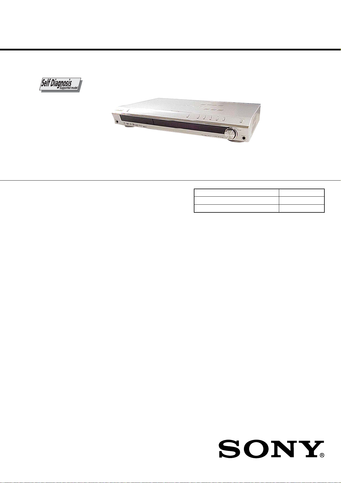
HCD-DZ700FW
Amplifier section
Stereo mode (rated) 55 W + 55 W (3 ohms at 1
kHz, DIN)
Surround mod e (refe r ence) musi c power output
Front: 143 W + 143 W
(with SS-TS46)
Center*: 143 W
(with SS-CT46)
Surround*: 143 W + 143
W
(with SS-TS46B)
Subwoofer*: 285 W
(with SS-WS42)
*Depending on the sound field settings and the source,
there may be no sound output.
Inputs (Analog)
TV, VIDEO Sensitivity: 450 mV
Impedance: 50 kilohm s
Inputs (Digital)
VIDEO (Optical)
SAT (Coaxial) Impedance: 75 oh ms
AUDIO IN
Sensitivity: 250/125 mV
Impedance: 50 kilohm s
Phones Accepts low-and high-
impedance headphones.
Super Audio CD/DVD system
Laser Semiconductor laser
(Super Audio CD/DVD:
= 650 nm)
(CD: = 790 nm)
Emission duration:
continuous
Signal format system PAL/NTSC
Frequency response (at 2 CH STEREO mode)
DVD (PCM): 2 Hz to 22
kHz (±1.0 dB)
CD: 2 Hz to 20 kHz (±1.0
dB)
Harmonic distortion Less than 0.03 %
Tuner section
System PLL quartz-locked digital
synthesizer system
FM tuner section
Tuning range 87.5 – 108.0 MHz (50 kHz
step)
Antenna (aerial) FM wire antenna ( aerial)
λ
λ
Antenna (aerial) terminals 75 ohms, unbalanced
Intermediate frequency 10.7 MHz
AM tuner section
Tuning range 531 – 1,602 kHz (with the
interval set at 9 kHz)
Antenna (aerial) AM loop antenna (aerial)
Intermediate frequency 450 kHz
Video section
Outputs Video: 1 Vp-p 75 ohms
R/G/B: 0.7 Vp-p 75 ohms
COMPONENT:
Y: 1 Vp-p 75 ohms
PB/CB, PR/CR: 0.7 Vp-p
75 ohms
Input VIDEO: 1 Vp-p 75 ohms
General
Power requirements 220 – 240 V AC, 50/60 Hz
Power consumption On: 130 W
Standby: 0.3 W (at the
Power Saving mode)
Dimensions (approx.) 430 70 295 mm (w/h/d)
××
incl. projecting parts
Mass (approx.) 3.6 kg
Design and specifications are subject to change
without notice.
SERVICE MANUAL
Ver. 1.0 2005.05
HCD-DZ700FW is the amplifier, D VD/CD and
tuner section in DAV-DZ700FW.
This system incorporates with Dolby*1 Digital and Dolby Pro Logic
(II) adaptive matrix surround decoder and the DTS*2 Digital
Surround System.
*1 Manufactured under license from Dolby Laboratories.
“Dolby, ” “Pro Logic, ” and the double-D symbol are trademarks
of Dolby Laboratories.
*2 Manufactured under license from Digital Theater Systems, Inc.
“DTS” and “DTS Digital Surround” are trademarks of
Digital Theater Systems, Inc.
AEP Model
UK Model
Model Name Using Similar Mechanism HCD-DZ300
Mechanism T ype CDM85-DVBU102
Optical Pick-up Name
KHM-310CAA
9-879-676-01
2005E1678-1
© 2005.05
Sony Corporation
Audio Group
Published by Sony Engineering Corporation
SPECIFICATIONS
SUPER AUDIO CD/DVD RECEIVER
HCD-DZ700FW
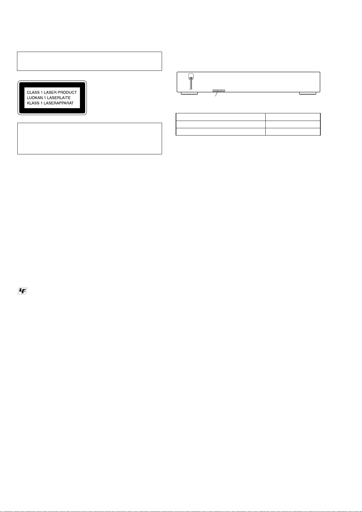
Laser component in this product is capable of emitting radiation
exceeding the limit for Class 1.
This appliance is classified as
a CLASS 1 LASER product.
The CLASS 1 LASER
PRODUCT MARKING is
located on the rear exterior.
CAUTION
Use of controls or adjustments or performance of procedures
other than those specified herein may result in hazardous radiation
exposure.
Notes on chip component replacement
• Never reuse a disconnected chip component.
• Notice that the minus side of a tantalum capacitor may be
damaged by heat.
Flexible Circuit Board Repairing
• Keep the temperature of the soldering iron around 270 °C
during repairing.
• Do not touch the soldering iron on the same conductor of the
circuit board (within 3 times).
• Be careful not to apply force on the conductor when soldering
or unsoldering.
MODEL IDENTIFICATION
– Rear Panel –
Parts No.
Model Part No.
AEP and UK models 2-588-157-0[]
RU model 2-588-157-1[]
•Abbreviation
RU : Russian model.
UNLEADED SOLDER
Boards requiring use of unleaded solder are printed with the leadfree mark (LF) indicating the solder contains no lead.
(Caution: Some printed circuit boards may not come printed with
the lead free mark due to their particular size)
: LEAD FREE MARK
Unleaded solder has the following characteristics.
• Unleaded solder melts at a temperature about 40 °C higher
than ordinary solder.
Ordinary soldering irons can be used but the iron tip has to be
applied to the solder joint for a slightly longer time.
Soldering irons using a temperature regulator should be set to
about 350 °C.
Caution: The printed pattern (copper foil) may peel away if
the heated tip is applied for too long, so be careful!
• Strong viscosity
Unleaded solder is more viscou-s (sticky, less prone to flow)
than ordinary solder so use caution not to let solder bridges
occur such as on IC pins, etc.
• Usable with ordinary solder
It is best to use only unleaded solder but unleaded solder may
also be added to ordinary solder.
SAFETY-RELATED COMPONENT WARNING!!
COMPONENTS IDENTIFIED BY MARK 0 OR DOTTED LINE
WITH MARK 0 ON THE SCHEMATIC DIAGRAMS AND IN
THE PARTS LIST ARE CRITICAL TO SAFE OPERATION.
REPLACE THESE COMPONENTS WITH SONY PAR TS WHOSE
PART NUMBERS APPEAR AS SHOWN IN THIS MANU AL OR
IN SUPPLEMENTS PUBLISHED BY SONY.
2

TABLE OF CONTENTS
HCD-DZ700FW
1. SERVICING NOTE ................................................... 4
2. GENERAL ................................................................... 6
3. DISASSEMBLY
3-1. Disassembly Flow ........................................................... 8
3-2. Case, Front Panel Assy .................................................... 9
3-3. FL Board, H/P Board....................................................... 10
3-4. STBY Board, KEY Board ............................................... 10
3-5. I/O Board, DC Fan .......................................................... 11
3-6. TX Board ......................................................................... 11
3-7. DMB10 Board ................................................................. 12
3-8. MAIN Board.................................................................... 12
3-9. DVD Mechanism Deck (CDM85-DVBU102) ................ 13
3-11. Belt, MS-203 Board ........................................................ 14
3-12. Base Unit ......................................................................... 15
3-13. Optical Pick-up (KHM-310CAA) ................................... 15
4. TEST MODE ............................................................... 16
5. ELECTRICAL ADJUSTMENT ............................. 20
6. DIAGRAMS
6-1. Block Diagram – RF/SERVO Section –......................... 22
6-2. Block Diagram – VIDEO Section – ............................... 23
6-3. Block Diagram – AMP Section –................................... 24
6-4. Block Diagram – AUDIO Section – ............................... 25
6-5. Block Diagram – POWER Section –.............................. 26
6-6. Block Diagram – DIAT TRANSMIT Section – ............. 27
6-7. Printed Wiring Board – DMB10 Board (Side A) – ......... 28
6-8. Printed Wiring Board – DMB10 Board (Side B) – ......... 29
6-9. Schematic Diagram – DMB10 Board (1/4) –................. 30
6-10. Schematic Diagram – DMB10 Board (2/4) –................. 31
6-11. Schematic Diagram – DMB10 Board (3/4) –................. 32
6-12. Schematic Diagram – DMB10 Board (4/4) –................. 33
6-13. Printed Wiring Board – MAIN Board (Side A) –............ 34
6-14. Printed Wiring Board – MAIN Board (Side B) –............ 35
6-15. Schematic Diagram – MAIN Board (1/8) – ................... 36
6-16. Schematic Diagram – MAIN Board (2/8) – ................... 37
6-17. Schematic Diagram – MAIN Board (3/8) – ................... 38
6-18. Schematic Diagram – MAIN Board (4/8) – ................... 39
6-19. Schematic Diagram – MAIN Board (5/8) – ................... 40
6-20. Schematic Diagram – MAIN Board (6/8) – ................... 41
6-21. Schematic Diagram – MAIN Board (7/8) – ................... 42
6-22. Schematic Diagram – MAIN Board (8/8) – ................... 43
6-23. Printed Wiring Boards – FRONT PANEL Section –....... 44
6-24. Schematic Diagram – FRONT PANEL Section –.......... 45
6-25. Printed Wiring Boards – AUDIO IN/OUT Section – ...... 46
6-26. Schematic Diagram – AUDIO IN/OUT Section – ......... 47
6-27. Printed Wiring Board – I/O Board (Side A) – ................. 48
6-28. Printed Wiring Board – I/O Board (Side B) –................. 49
6-29. Schematic Diagram – I/O Board (1/2) – ........................ 50
6-30. Schematic Diagram – I/O Board (2/2) – ........................ 51
6-31. Printed Wiring Board – MS-203 Board –........................ 52
6-32. Schematic Diagram – MS-203 Board – ......................... 52
6-33. Printed Wiring Board – TX Board –................................ 53
6-34. Schematic Diagram – TX Board – ................................. 54
7. EXPLODED VIEWS
7-1. Overall Section ................................................................ 68
7-2. Front Panel Section ......................................................... 69
7-3. Chassis Section................................................................ 70
7-4. DVD Mechanism Deck Section (CDM85-DVBU102) ... 71
8. ELECTRICAL PARTS LIST .................................. 72
3
HCD-DZ700FW
SECTION 1
SERVICING NOTE
NOTES ON HANDLING THE OPTICAL PICK-UP BLOCK
OR BASE UNIT
The laser diode in the optical pick-up block may suffer electrostatic
break-down because of the potential difference generated by the
charged electrostatic load, etc. on clothing and the human body.
During repair, pay attention to electrostatic break-down and also
use the procedure in the printed matter which is included in the
repair parts.
The flexible board is easily damaged and should be handled with
care.
NOTES ON LASER DIODE EMISSION CHECK
The laser beam on this model is concentrated so as to be focused on
the disc reflective surface by the objective lens in the optical pickup block. Therefore, when checking the laser diode emission,
observe from more than 30 cm away from the objective lens.
LASER DIODE AND FOCUS SEARCH OPERATION
CHECK
Carry out the “S curve check” in “CD section adjustment” and check
that the S curve waveform is output several times.
Self-diagnosis Function
DISC SLOT LOCK
The disc slot lock function for the antitheft of an demonstration
disc in the store is equipped.
Setting Procedure :
1. Press the ?/1 button to turn the set on.
2. Press the [FUNCTION] button to set DVD function.
3. Insert a disc.
4. Press the
x stick and the A button simultaneously for five
seconds.
5. The message “LOCKED” is displayed and the slot is locked.
Releasing Procedure :
1. Press the x stick and the A button simultaneously for five
seconds again.
2. The message “UNLOCKED” is displayed and the slot is
unlocked.
Note: When “LOCKED” is displayed, the slot lock is not released by
Note 1: Regarding the notification symbol “R”
Note 2: Incorrect operations may be performed if the test mode ia not
Note 3: If the disc tray does not open and the message “LOCKED”
turning power on/off with the ?/1 button.
Because the number of the operating buttons of this product are
limited, some operations require use of the operating buttons of
the remote commander, When a specific operation requires use
of the operating buttons of the remote commander, “R” is added
to the specific operating procedure in this manual.
Example MENU/NO “R” The MENU/NO button of remote
commander.
entered properly.
In this case, press the ?/1 button to turn the power off, and
retry to enter the test mode.
appears, press the x stick and the A button simultaneously
for seconds or longer.
Then remove your fingers from the above stick and the button.
The message “UNLOCKED” appears for 2 seconds and the disc
tray opens.
(When letters/numbers appear in the
display)
When the s elf -diagnosis function is acti vate d to
prevent the system from malfunctioning, a 5character service number (e.g., C 13 50) with a
combination of a letter and 4 digits appears on
the screen and the front pa nel display. In this
case, check the following table.
C:13:50
First 3
characters of
the servic e
number
C 13 The disc is dirty.
C 31 The disc is not inserted correc t ly.
E XX
(xx is a number)
Cause and/or corrective action
,Clean the disc with a soft cloth
,Restart the system, then re-insert
the disc correctly.
To prevent a malfunction, the
system has performed the selfdiagnosis function.
,Contact your nearest Sony
dealer or local authorized Sony
service facility and giv e the 5character service number.
Example: E 61 10
4
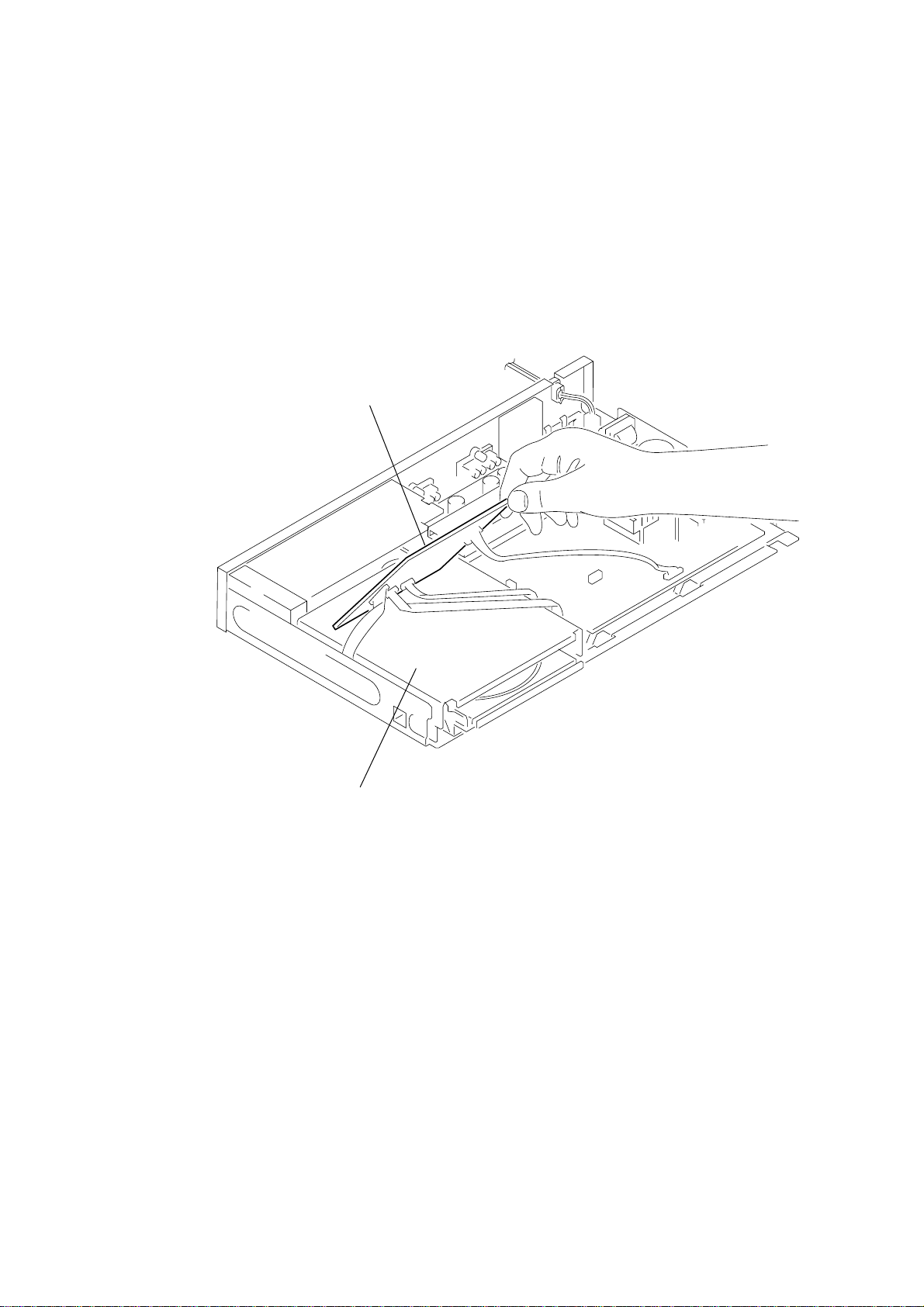
• SERVICE POSITION (DMB10 BOARD)
When servicing side B of the DMB10 board
Remove the DMB10 board from bracket.
(Refer to DISASSEMBLY 3-7. (page 12)).
Set the DMB10 board facing the side B upward as shown.
Connect the cable and make the repair work.
DMB10 board (side B)
HCD-DZ700FW
DMB bracket
5
HCD-DZ700FW
Front panel
SECTION 2
GENERAL
This section is extracted
from instruction manual.
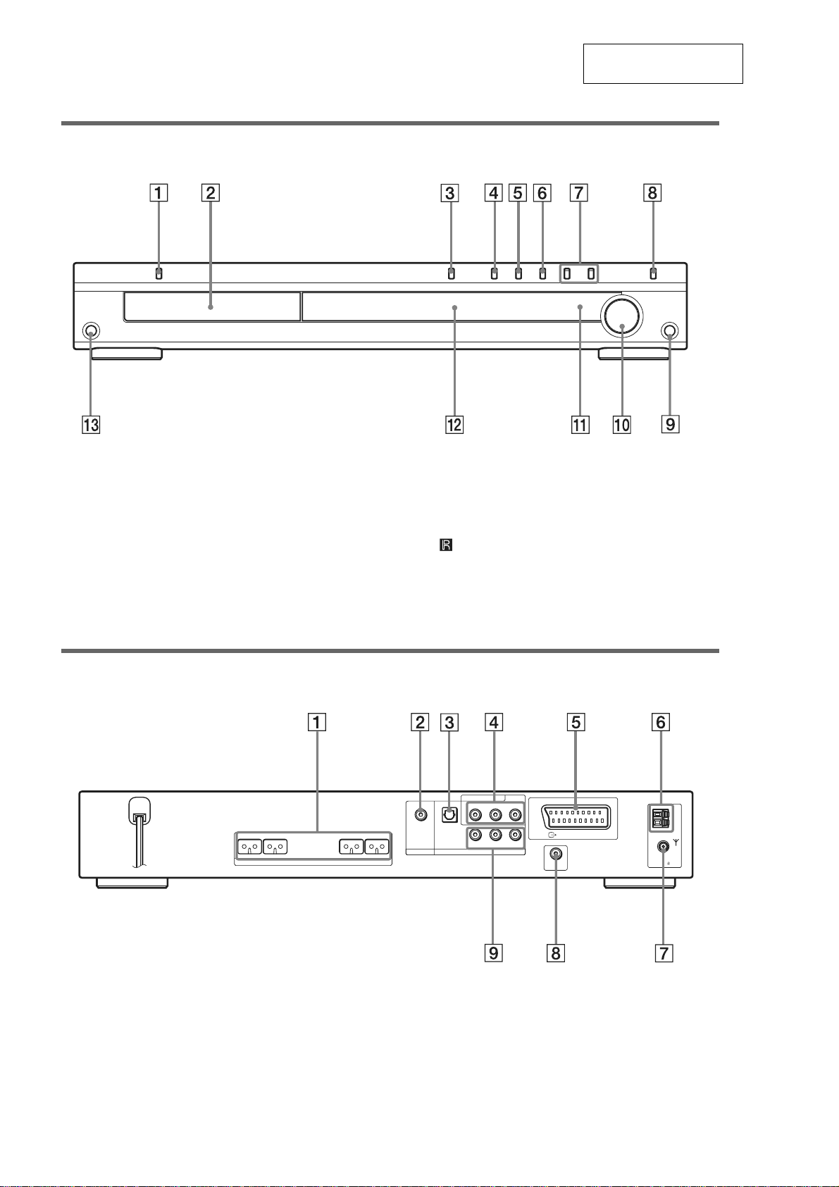
A "/1 (on/standby) (32, 39, 82)
B Disc tray (39)
C A (open/close) (39, 82)
D H (play) (39)
E X (pause) (39)
F x (stop) (39, 82)
G ./> (39)
Rear panel
FRONT R FRONT L CENTER WOOFER
SPEAKER
H FUNCTION (39)
I PHONES jack (39)
J VOLUME (39)
K (remote sensor) (13)
L Front panel dis play ( 1 0 1)
M AUDIO IN jack
Y
RAUDIO IN VIDEO INL
DVD ONLY
PB/CBPR/C
R
EURO AV
OUTPUT(TO TV)
DIR-T1
COMPONENT VIDEO OUT
OPTICAL
COAXIAL
DIGITAL IN
DIGITAL IN
SAT VIDEO
COAXIAL
FM
AM
75
A SPEAKER jacks (15)
B SAT COAXIAL DIGITAL IN jack (30)
C VIDEO OPTICAL DIGITAL IN jack (30)
D COMPONENT VIDEO OUT jacks (26)
E EURO AV T OUTPUT (TO TV) jacks
(26)
6
F AM terminal (25)
G FM 75 COAXIAL jack (25)
Ω
H DIR-T1 jack (15)
I VIDEO VIDEO/AUDIO IN jacks (28, 30)
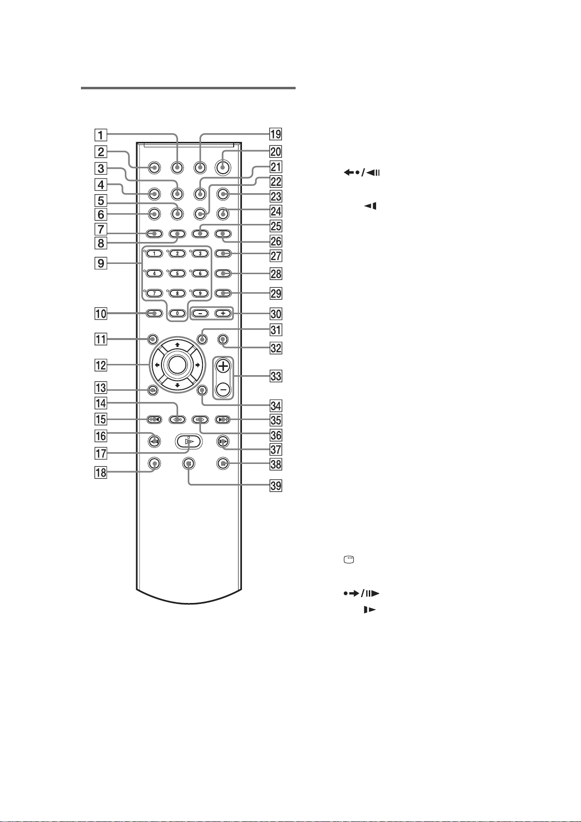
Remote
HCD-DZ700FW
J CLEAR, - (35, 41, 75, 76)
K TOP MENU (43)
L C/X/x/c/ENTER (32, 41, 65, 71, 77, 82,
83)
M O RETURN (45)
N REPLAY, STEP (39)
O . PRESET –, TV CH – (35, 39, 75, 79)
P m/ SLOW, TUNING – (55, 79)
Q H (play) (39)
The H button has a tactile dot.*
R TV (75)
S THEATRE SYNC (76)
T "/1 (on/standby) (32, 39, 79)
U AMP MENU (32, 77, 82)
V DSGX (68)
W FUNCTION (27, 39, 68, 77)
X SOUND FIELD (65)
Y DISPLAY (79)
Z PICTURE NAVI (49)
wj AUDIO (63)
wk SUBTITLE (70)
wl ANGLE (70)
e; ALBUM –/+ (39, 76)
ea MENU (43)
es MUTING (39)
ed VOLUME, TV VOL +/– (39, 75, 79)
The VOLUME, TV VOL + button has a
tactile dot.*
ef DISPLAY (10, 35, 41, 71, 83)
eg > PRESET +, TV CH + (35, 39, 75, 79)
A TV [/1 (on/standby) (75)
B TV/VIDEO (75)
C TUNER MENU (79)
D SLEEP (81)
E SA-CD/CD (44)
F PROGRESSIVE (27)
G REPEAT/FM MODE (42, 79)
H MULTI/2CH (44)
I Number buttons (43, 71, 75)
The number 5 but t on has a tactile dot.*
eh ADVANCE, STEP (39)
ej M/ SLOW, TUNING + (55, 79)
ek x (stop) (39, 71, 79)
el X (pause) (39)
*Use the tactile dot as a ref erence when operat ing the
system.
7
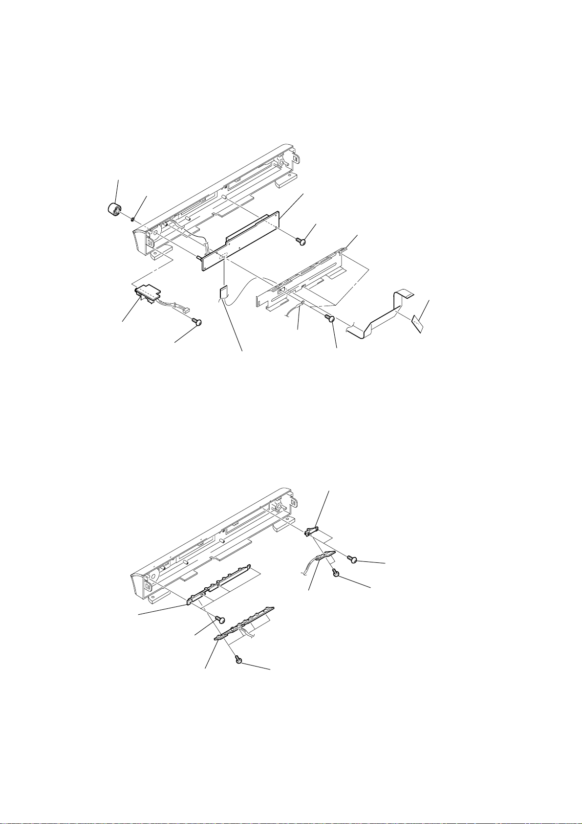
HCD-DZ700FW
SECTION 3
DISASSEMBLY
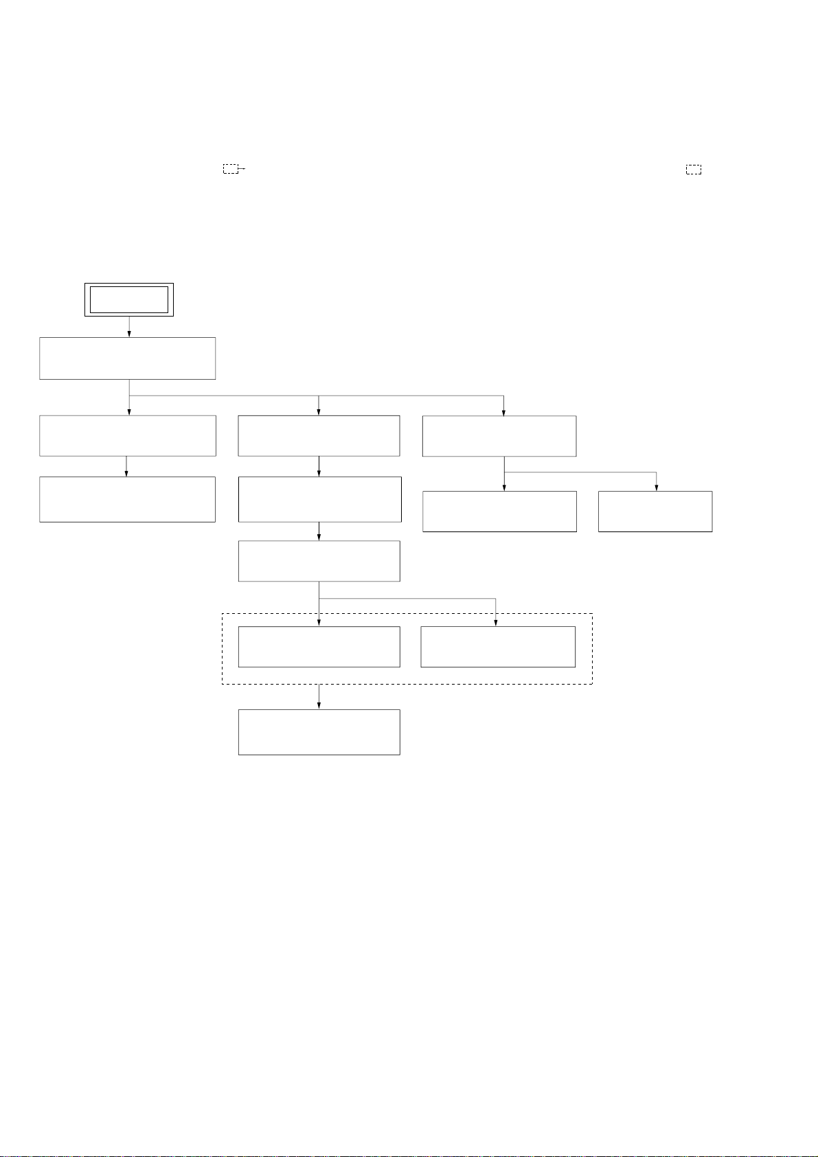
3-1. DISASSEMBLY FLOW
•This set can be disassembled in the order shown below.
•The dotted square with arrow ( ) prompts you to move to the next job when all of the works within the dotted square ( ) are
completed.
SET
3-2. CASE, FRONT PANEL ASSY
(Page 9)
3-3. FL BOARD, H/P BOARD
(Page 10)
3-4. STBY BOARD, KEY BOARD
(Page 10)
3-7. DMB10 BOARD
(Page 12)
3-9. DVD MECHANISM DECK
(CDM85-DVBU102)
(Page 13)
3-10. TRAY
(Page 13)
3-12. BASE UNIT
(Page 15)
3-13. OPTICAL PICK-UP
(KHM-310CAA)
(Page 15)
3-5. I/O BOARD, DC FAN
(Page 11)
3-6. TX BOARD
(Page 11)
3-11. BELT, MS-203 BOARD
(Page 14)
3-8.MAIN BOARD
(Page 12)
8
Note: Follow the disassembly procedure in the numerical order given.
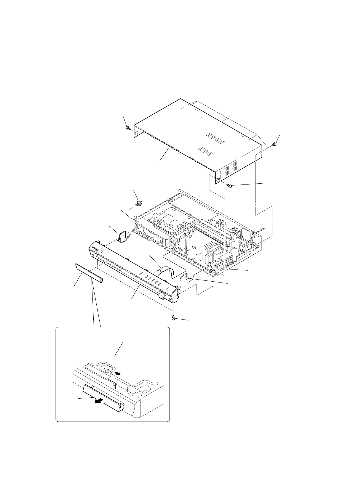
3-2. CASE, FRONT PANEL ASSY
4
screw (CASE3 TP2)
7
case
qd
floating
screw (+PTPWH M2.6)
HCD-DZ700FW
6
five screws (+BVTP 3 × 8)
5
screw
(CASE3 TP2)
3
DVD lid assy
9
claw
qf
IPOD board
qs
w
ire (flat type)
19core(CN509)
qg
front panel assy
1
The lever is moved in the direction
of the arrow with the thin rod.
qa
connector
(CN309)
8
three screws (+BVTP 3 × 8)
0
claw
DVD lid
2
9
HCD-DZ700FW
3-3. FL BOARD, H/P BOARD
3
knob (vol)
4
nut
qa
FL board
9
t
apping screw
(DIA.2.6
×
8)
8
shield (front)
5
sheet
2
H/P board
1
(DIA.2.6
3-4. STBY BOARD, KEY BOARD
4
button (play)
t
apping screw
×
8)
7
earth line
q;
wire (flat type)
19core(CN801)
7
STBY board
6
three t
(DIA.2.6
8
button (power)
apping screws
×
8)
5
two tapping screws
(DIA.2.6
6
two tapping screws
(DIA.2.6
×
8)
×
8)
10
1
four tapping screws
(DIA.2.6
×
8)
3
KEY board
2
four tapping screws
(DIA.2.6
×
8)
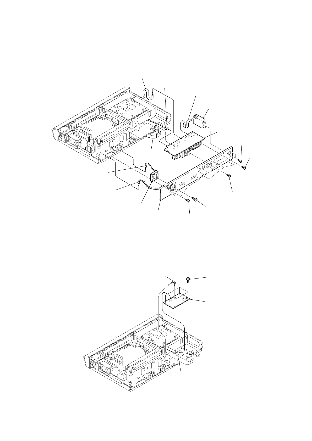
3-5. I/O BOARD, DC FAN
3
wire (flat type)
13core(CN201)
6
wire (flat type)
23core(CN601)
5
connector
(CN602)
0
wire (flat type)
11core or 9core (CN101)
qd
tuner
qa
I/O board
qs
two screws (+BVTP 3 × 8)
HCD-DZ700FW
0
two
screws
(+BVTP 3 × 8)
3-6. TX BOARD
2
connector
(CN300)
1
connector
(CN901)
8
DC fan
back panel
3
connector
(CN802)
7
two screws (BVTT 4 × 8)
4
six
screws (+BVTP 3 × 8)
1
four screws (+BV 3)
4
TX
9
four
screws (+BVTP 3 × 8)
board
2
wire (flat type)
13core(CN801)
11
HCD-DZ700FW
)
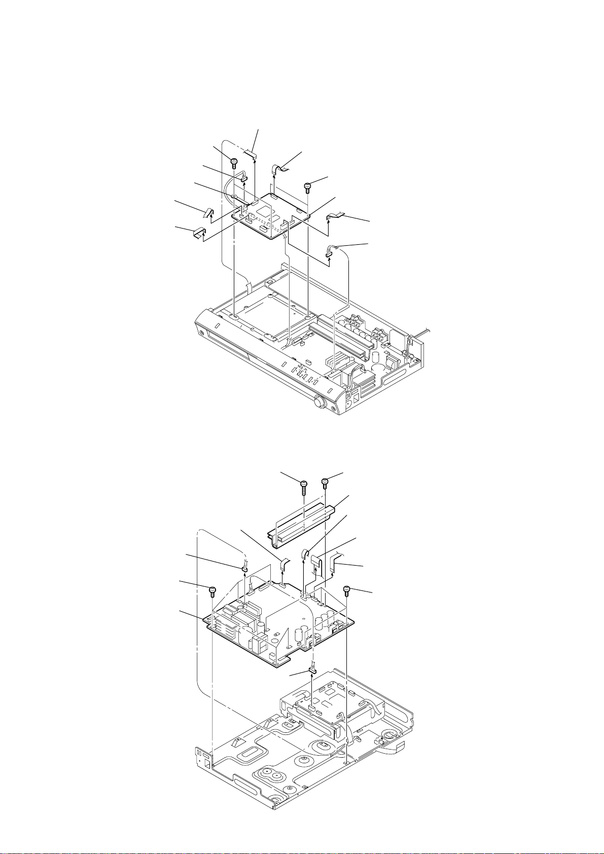
3-7. DMB10 BOARD
2
7core(CN202)
1
11core(CN106)
8
two screws (+BV 3)
3
(CN201)
9
coating clip
wire (flat type)
wire (flat type)
connector
4
wire (flat type)
24core(CN101)
5
13core(CN301)
wire (flat type)
0
two screws (+BV 3)
qa
DMB10 board
6
wire (flat type)
11core(CN4501
7
connector
(CN401)
3-8. MAIN BOARD
0
five screws (+BV 3)
8
(CN902)
qs
MAIN board
connector
2
screw (BVTP 3 × 12)
4
wire (flat type)
11core(CN505)
9
connector
(CN401)
1
two screws (+BV 3)
3
heat sink (AMP)
5
wire (flat type)
11core(CN512)
6
23core(CN507)
wire (flat type)
7
wire (flat type)
11core(CN504)
qa
four screws (+BV 3)
12
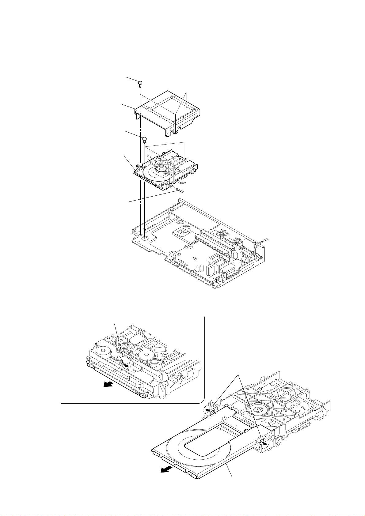
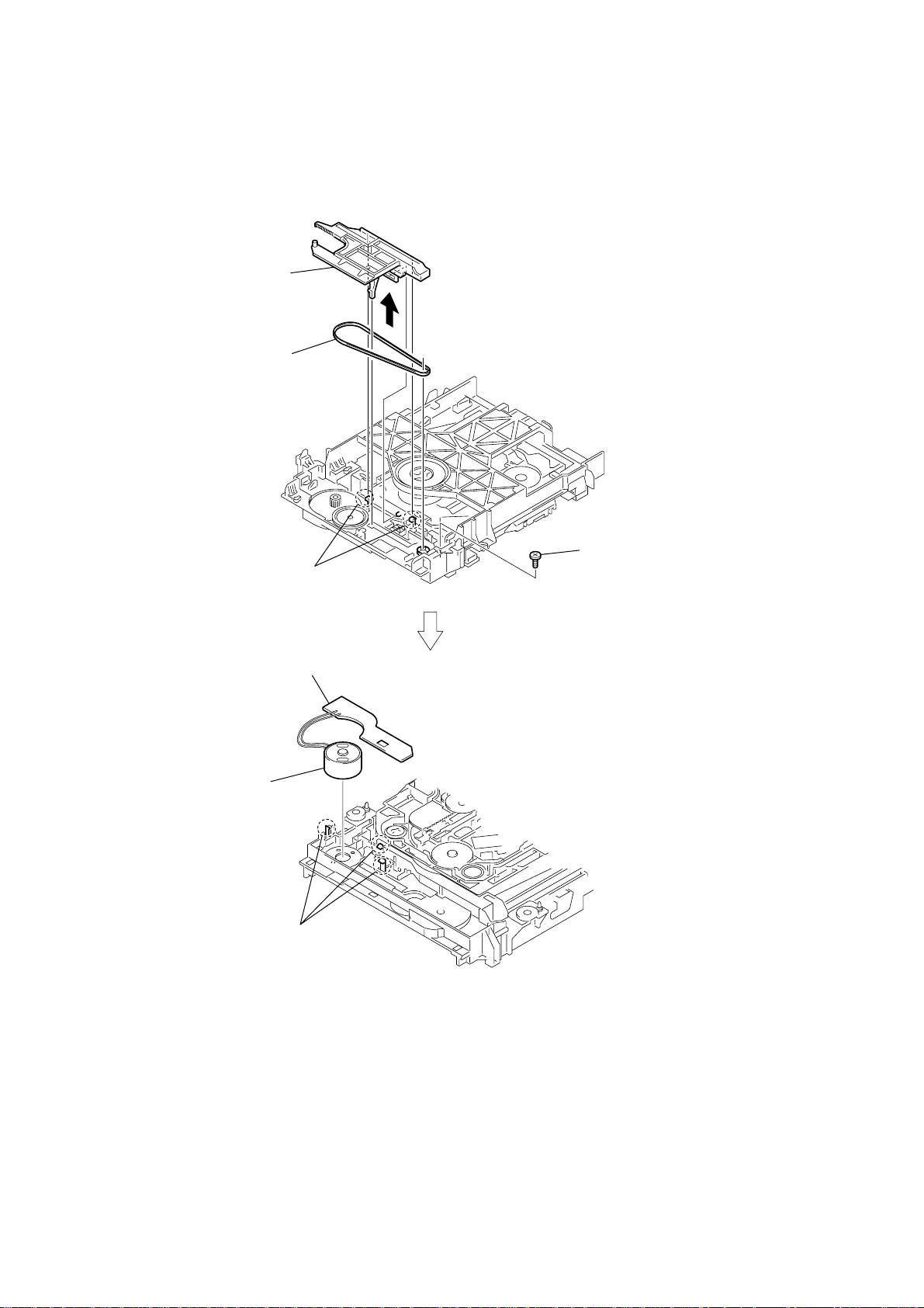
3-9. DVD MECHANISM DECK (CDM85-DVBU102)
1
t
hree screws (+BV 3)
2
dmb bracket
3
three
screws (+BV 3)
5
DVD mechanism deck
(CDM85-DVBU102)
HCD-DZ700FW
3-10. TRAY
1
Move the Chuck cam
in the direction of the arrow.
4
wire (flat type)
5 core
bottom side
3
two claws
2
4
5
tray
13
HCD-DZ700FW
3-11. BEL T, MS-203 BOARD
2
chuck cam
3
belt
6
DC motor
1
two claws
7
MS-203 board
5
three claws
4
screw
(M 1.7
×
2.5)
14
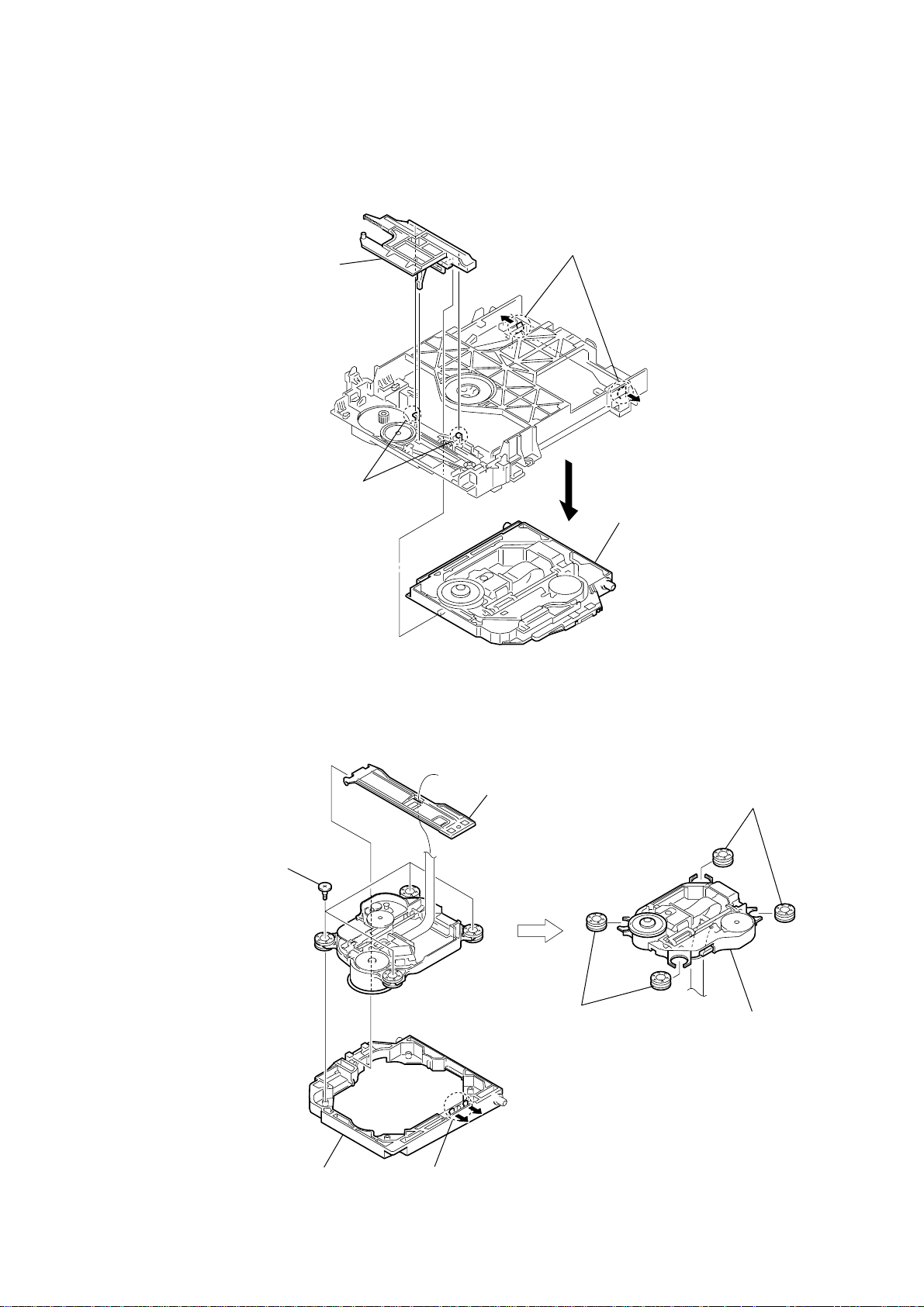
3-12. BASE UNIT
s
2
chuck cam
3
two claws
HCD-DZ700FW
1
two claws
3-13. OPTICAL PICK-UP (KHM-310CAA)
3
four insulator screws
2
loading base
4
base unit
4
two insulator
bu holder
1
two claws
5
two insulators
6
optical pick-up
(KHM-310CAA)
15

HCD-DZ700FW
SECTION 4
TEST MODE
Note 1: Regarding the notification symbol “R”
Because the number of the operating buttons of this product
are limited, some operations require use of the operating
buttons of the remote commander, When a specific operation
requires use of the operating buttons of the remote
commander, “R” is added to the specific operating procedure
in this manual. Example MENU/NO “R” The MENU/NO
button of remote commander.
Note 2: Incorrect operations may be performed if the test mode is
not entered properly.
In this case, press the ?/1 button to turn the po wer of f, and
retry to enter the test mode.
1. Cold Reset
• The cold reset clears all data including preset data stored in
the RAM to initial conditions. Execute this mode when
returning the set to the customers.
Procedure:
1. Press the ?/1 button to turn the power on.
2. Press three buttons x , A and ?/1 simultaneously.
3. When this button is operated, display as “COLD RESET” for
a while and all of the settings are reset.
2. Panel Test Mode
•This mode is used to check the software version, LCD, LED
and keyboard.
2-1. DVD LED Test Mode
Procedure:
1. Press the ?/1 button to turn on the power.
2. Press three bottons X , . and A simultaneously.
3. When the display LED test mode is activated, all segments
are turned on.
4. To exit from this mode, pull out the AC plug.
2-2. V ersion T est Mode
Procedure:
1. When the panal test mode is activated, press the . button
and the message “DS6W***” is displayed, the version test
mode is activated.
2. Whenever press the . button, the version is displayed in
order of CC2, MC, SYS, UI, DVD, TA, TM and DS6W.
3. Press the > button and the date of the softwafe production
is displayed.
4. Press the > button again and the version is displayed.
5. To exit from this mode, pull out the AC plug.
2-3. Key Test Mode
Procedure:
1. When the panel test mode is activated, press the H button,
to select the key test mode.
2. To enter the KEY test mode, the fluorecent indicator displays
“K0 VO”. Each time a button is pressed, “KEY” value
increases. However, once a button is pressed, it is no longer
taken into account. When all keys are pressed correctly, “K8
VO” is displayed.
3. To exit from this mode, pull out the AC plug.
3. Disc Tray Lock
The disc tray lock function for the antitheft of an demonstration
disc in the store is equipped.
Setting Procedure :
1. Press the ?/1 button to turn the set on.
2. Press the FUNCTION button to set DVD function.
3. Insert a disc.
4. Press the x button and the A button simultaneously for fiv e
seconds.
5. The message “LOCKED” is displayed and the tray is locked.
Releasing Procedure :
1. Press the x button and the A button simultaneously for fiv e
seconds. again.
2. The message “UNLOCKED” is displayed and the tray is
unlocked.
Note: When “LOCKED” is displayed, the slot lock is not released by
turning power on/off with the ?/1 button.
4. DVD Ship Mode
• Use this mode when returning the set to the customer after
repair.
Procedure:
1. Press the ?/1 button to turn the set on.
2. Press the FUNCTION button to set the function “DVD”.
3.
Press three buttons x
4. After a message “MECHA LOCK” is displayed on the
fluorescent indicator tube, pull out the AC plug.
5. To exit from this mode, press the ?/1 button to turn the set
on.
5. DVD Debug In Mode
Procedure:
1. Press the ?/1 button to turn the set on.
2. Press the FUNCTION button to set the function “DVD”.
3. Press the three buttons . , A and > simultaneously.
4. To exit from this mode, press the ?/1 button to turn the set
on.
6. AM Step Change
•A step of AM channels can be changed over between 9 kHz
and 10 kHz.
Procedure:
1. Press ?/1 button to turn the set ON.
2. Select the function “TUNER”, and press FUNCTION button
to select the BAND “AM”.
3. Press ?/1 button to turn the set OFF.
4. Press > and ?/1 buttons simultaneously , and the display
of fluorescent indicator tube changes to “AM 9 k STEP” or
“AM 10 k STEP”, and thus the channel step is changed over.
,
and
?/1
simultaneously.
16

HCD-DZ700FW
DVD SECTION
4-1. GENERAL DESCRIPTION
The Mirror Time and IOP measurement allows you to make
diagnosis and adjustment simply by using the remote commander
and monitor TV. The instructions, diagnosis results, etc. are given
on the on screen display (OSD).
The Mirror Time and IOP measurement is required is such events
where servicing a DVD-Player includes changing the Base Unit
(BU). For each new BU to be used with a certain MV-044 board,
Mirror Time and IOP measurement need to be carried out.
4-2. STARTING TEST MODE
Press three buttons x , A and VOLUME + simultaneously
with the DVD player in standby mode.
The Test Mode starts, then the menu shown below will be
displayed on the TV screen.
Remocon Diagnosis Menu
0. External Chip Check
1. Servo Parameter Check
2. Drive Manual Operation
3. Emergency History
4. Version Information
5. Video Level Adjustment
4-4. MIRROR TIME ADJUSTMENT
To enter Mirror Time Adjustment, press 5 “R” button on the remote
commander. The screen will appear as below.
MIRR time Adjust Menu
1. CD MIRR time Check:
2. DVD MIRR time Check:
3. Threshold:
4. Save to EEPROM
5. Default set MIRR time
[Open] Tray open [Close] Tray close
[0] Return to previous menu
There are five main commands in the Mirr time Adjust menu as
shown in the figure above. The functions of each command are
described in the following page.
1. CD MIRR time Check
This command checks the Mirror time value for CD disc.
2. DVD MIRR time Check
This command checks the Mirror time value for DVD disc.
3. Threshold
This command displays the threshold value between CD and DVD
mirror time.
Model Name : DS6W_XX
IF-con : V
Syscon : Ver.
er. xx.xx (xxxx)
x.xxx
The menu above is the Remocon Diagnosis Menu screen which
consists of six main function. At the bottom of the menu screen,
the model name and IF-con version. To enter Mirror Time
Adjustment menu, press button 2 “R” on the remote commander
to enter Drive Manual Operation menu. To exit from the Test Mode,
press the power button on the remote commander.
4-3. DRIVE MANUAL OPERATION
The Drive Manual Operation menu consists of five main
function. By pressing 2 “R” button on the remote commander in
the Remocon Diagnosis Menu, the screen will appear as below.
Drive Manual Operation
1. Servo Control
2. Track/Layer Jump
3. Manual Adjustment
4. Tray Aging Mode
5. MIRR time Adjust
0. Return to Top Menu
4. Save to EEPROM
This command saves an adjusted mirror time value to the EEPR OM.
5. Default set MIRR time
This command will set CD and DVD mirror time to firmware def ault
value.
[Open] / [Close]
Pressing the A button controls the tray for disc change
during mirror time adjustment.
[0] Return to previous menu
Press 0 “R” button to return to previous menu.
4-4-1. EXECUTING MIRROR TIME ADJUSTMENT
In order to execute mirror time adjustment, the following standard
procedures must be followed.
(1) In standby mode, press three buttons x , A and
VOLUME + simultaneously.
(2) Select “2. Drive Manual Operation”.
Remocon Diagnosis Menu
0. External Chip Check
1. Servo Parameter Check
2. Drive Manual Operation
3. Emergency History Check
4. Version information
5. Video Level Adjustment
Model : DS6W_xx
IF-con : Ver. xx.xx (xxxx)
Syscon : Ver. x.xxx
17

HCD-DZ700FW
(3) Select “5. MIRR time Adjust”.
Drive Manual Operation
1. Servo Control
2. Track/Layer Jump
3. Manual Adjustment
4. Mecha test mode
5. MIRR time Adjust
0. Return to Top Menu
(4) Select “5. Default set MIRR time”.
MIRR time Adjust Menu
1. CD MIRR time Check:
2. DVD MIRR time Check:
3. Threshold:
4. Save to EEPROM:
5. Default set MIRR time:
[Open] Tray open [Close] Tray close
[0] Return to previous menu
(5) Select “3. Threshold”.
(6) Confirm the number. If it is 7D, go to next step. If it is any
other value, return to step 4.
MIRR time Adjust Menu
(14) Confirm the same values are displayed. If it is not same,
return to step 7.
MIRR time Adjust Menu
1. CD MIRR time Check:
2. DVD MIRR time Check: XX XX
3. Threshold:
4. Save to EEPROM:
5. Default set MIRR time:
[Open] Tray open [close] Tray close
[0] Return to previous menu
(15) Push A button to eject tray.
(16) Take out HLX-504 and insert Test Disc YEDS-18 into
tray.
(17) Push A button to close tray.
(18) Push “1. CD MIRR time check”.
(19) Wait for HEX number to display.
(20) Confirm the number, if YY is 5A ~ E8, proceed with next
step. If no, return to 15.
MIRR time Adjust Menu
1. CD MIRR time Check:
2. DVD MIRR time Check:
3. Threshold: 7D
4. Save to EEPROM:
5. Default set MIRR time:
[Open] Tray open [Close] Tray close
[0] Return to previous menu
(7) Push A button to eject tray.
(8) Insert Test Disc HLX-504 into tray.
(9) Push A button to close tray.
(10) Push “2. DVD MIRR time Check”.
(11) Wait for HEX number to display.
(12) Confirm the number, if XX is 28 ~ 70, proceed with next
step. If no, return to 8.
MIRR time Adjust Menu
1. CD MIRR time Check:
2. DVD MIRR time Check: xx xx
3. Thereshold:
4. Save to EEPROM:
5. Default set MIRR time:
[Open] tray open [close] Tray close
[0] Return to previous menu
1. CD MIRR time Check: yy YY
2. DVD MIRR time Check: XX XX
3. Threshold:
4. Save to EEPROM:
5. Default set MIRR time:
[Open] Tray open [close] Tray close
[0] Return to previous menu
(21) Push “4. Save to EEPROM”.
(22) Confirm the same values are displayed. If it is not the
same, return to step 15.
MIRR time Adjust Menu
1. CD MIRR time check: YY YY
2. DVD MIRR time check: XX XX
3. Threshold:
4. Save to EEPROM:
5. Default set MIRR time:
[Open] Tray open [close] Tray close
[0] Return to previous menu
(23) Push A button to eject tray.
(24) Remove Test Disc YEDS-18 from tray.
(25) Push A button to close tray.
(26) Press 0 “R” button to the Drive Manual Operation menu.
(13) Push “4. Save to EEPROM”.
18
(27) Press 0 “R” button to return to the Remocon Diagnosis
Menu.
(28) Press the ?/1 button to switch OFF set.

HCD-DZ700FW
4-5. EXECUTING IOP MEASUREMENT
In order to execute mirror time adjustment, the following standard
procedures must be followed.
(1) In standby mode, press three buttons x , A and
VOLUME + simultaneously.
Remocon Diagnosis Menu
0. External Chip Check
1. Servo Parameter Check
2. Drive Manual Operation
3. Emergency History Check
4. Version information
5. Video Level Adjustment
Model : DS6W XX
IF-con Ver : XX.XX (XXXX)
Syscon Ver : X.XX
(2) Select “2. Drive Manual Operation” by pressing the 2 “R”
button on the remote commander. The screen will appear as
below.
Drive Manual Operation
1. Servo Control
2. Track/Layer Jump
3. Manual Adjustment
4. Tray Aging Mode
5. MIRR time adjust
0. Return to top Menu
(5) Wait until a hexadecimal number appear.
Manual Adjust
1. Track Balance Adjust:
2. Track Gain Adjust:
3. Focus Balance Adjust:
4. Focus Gain Adjust:
5. Eq Boost Adjust:
6. Iop. 5B:
7. TRV. Level:
8. S curve(FE) Level:
9. RFL(PI) Level:
0. MIRR Time:
Change Value
[0] Return to previous menu
(6) Convert each data from hexadecimal to decimal using
conversion table.
(7) Substract between these two values.
(8) If the remainder is smaller than 93 (decimal), then it is
OK. However if the value is higher than 93, then the BU
is defective and need to be change.
(9) Press RETURN “R” button to return back to previous menu.
(10) Press 0 “R” button to return to Top Menu and power OFF
the DVD Player.
(3) Select “3. Manual Adjustment” by pressing the 3 “R” b utton
on the remote commander. The screen will appear as below.
Manual Adjust
1. Track Balance Adjust:
2. Track Gain Adjust:
3. Focus Balance Adjust:
4. Focus Gain Adjust:
5. Eg boost Adjust:
6. Iop:
7. TRV. Level:
8. S curve(FE) Level:
9. RFL(PI) Level:
0. MIRR Time:
o O Change Value
[RETURN] Return to previous menu
(4) Select Iop by pressing 6 “R” button on the remote commander.
19
HCD-DZ700FW
SECTION 5
ELECTRICAL ADJUSTMENT
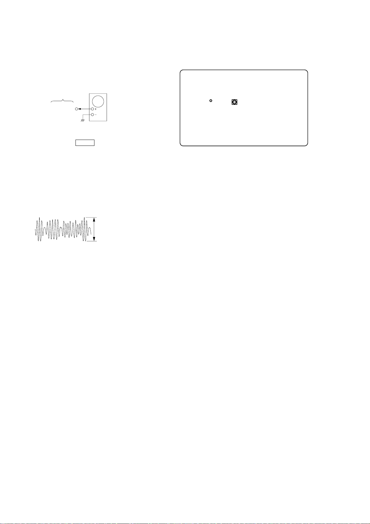
DIAT SIGNAL RF LEVEL ADJUSTMENT
This adjustment is performed in order to adjust the transmission
distance of RF signal for DIAT communication.
Connection:
TX board
TP815
Procedure:
1. Connect the oscilloscope to TP815 and GND on the TX board.
2. Connect DIR-T1 to DIR-T1 jack (J801).
3. Adjust RV801 on the TX board so that the center of w aveform
becomes 1.0 Vp-p.
4. Confirm trigger is locked.
5. Adjust RV801 on the TX board so that the center of w aveform
becomes 2.2 to 2.4 Vp-p.
RF Signal Reference Waveform
oscilloscope
VOLT/DIV : 500 mV
TIME/DIV : 500 ns
level : 2.2 to 2.4 Vp-p
Adjustment Location:
– TX Board (SIDE A) –
TP815
RV801
20
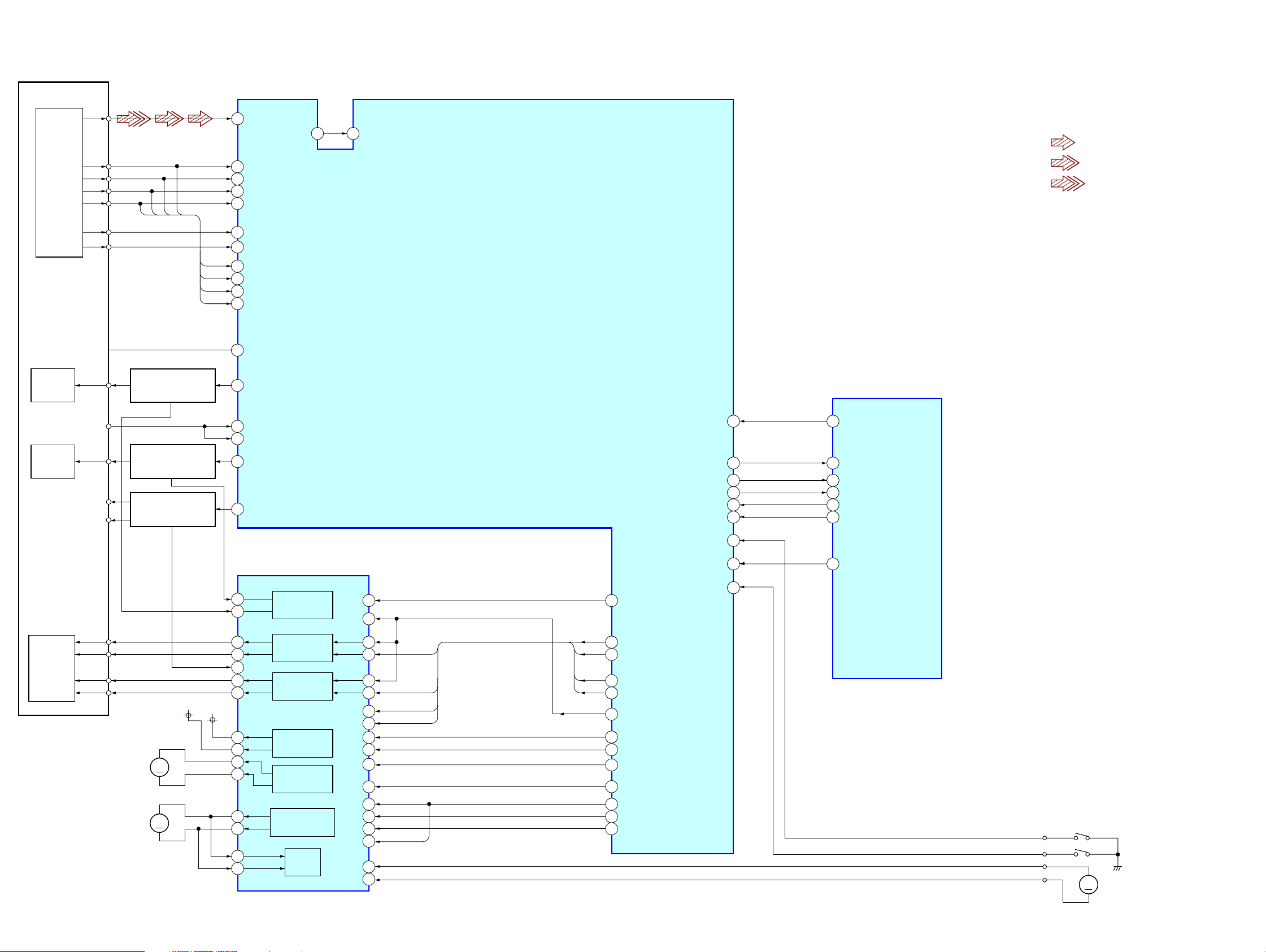
SECTION 6
d
DIAGRAMS
HCD-DZ700FW
THIS NOTE IS COMMON FOR PRINTED WIRING BOARDS AND SCHEMATIC DIAGRAMS.
(In addition to this, the necessary note is printed in each block.)
For Schematic Diagrams.
Note:
• All capacitors are in µF unless otherwise noted. (p: pF)
50 WV or less are not indicated except f or electrolytics and
tantalums.
• All resistors are in Ω and 1/
specified.
• f : internal component.
• C : panel designation.
Note: The components identified by mark 0 or dotted
line with mark 0 are critical for safety.
Replace only with part number specified.
✩ IC103 is a written in and settled EEPROM. Supply with
a single article has not been carried out. In case you
exchange by DMB10 board, please put on IC103
currently used with the model again.
• A : B+ Line.
• B : B– Line.
•Voltages and wavef orms are dc with respect to ground under no-signal (detuned) conditions.
•Voltages and waveforms are dc with respect to ground in
service mode.
•Waveforms are taken with a oscilloscope.
Voltage variations may be noted due to normal production
tolerances.
* : Impossible to measure
no mark : DVD STOP
•Voltages are taken with VOM (Input impedance 10 MΩ).
• Circled numbers refer to waveforms.
• Signal path.
F : AUDIO
J : CD PLAY
c : DVD PLAY
I : SACD PLAY
d : TUNER
L : VIDEO
E : Y
r : COMPONENT VIDEO
q : R, G, B
f : AUDIO IN
h : DIGITAL IN (OPTICAL IN)
i : DIGITAL IN (COAXIAL IN)
•Abbreviation
RU : Russian model.
4
W or less unless otherwise
For Printed Wiring Boards.
Note:
• X : parts extracted from the component side.
• a : Through hole.
•
(The other layers' patterns are not indicated.)
• Indication of transistor.
: Pattern from the side which enables seeing.
Caution:
Pattern face side: Parts on the pattern face side seen from
(SIDE A) the pattern face are indicated.
Parts face side: Parts on the parts face side seen from
(SIDE B) the parts face are indicated.
C
Q
CEB
These are omitte
E
B
These are omitted.
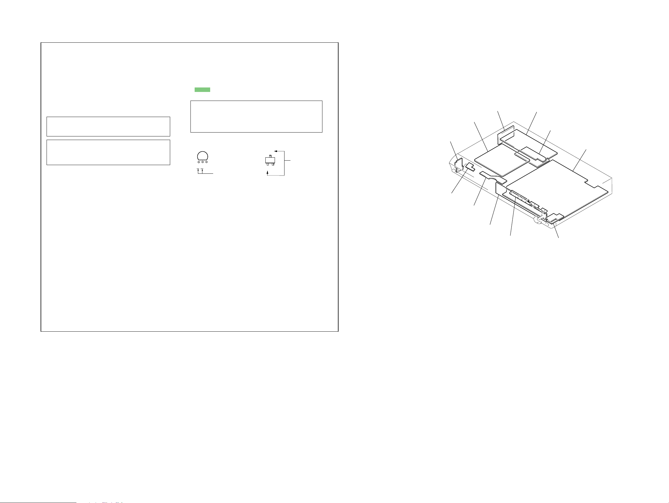
• Circuit Boards Location
IPOD board
STBY board
DMB10 board
MS-203 board
FL board
TUNER UNIT
KEY board
I/O board
TX board
MAIN board
H/P board
HCD-DZ700FW
2121
HCD-DZ700FW
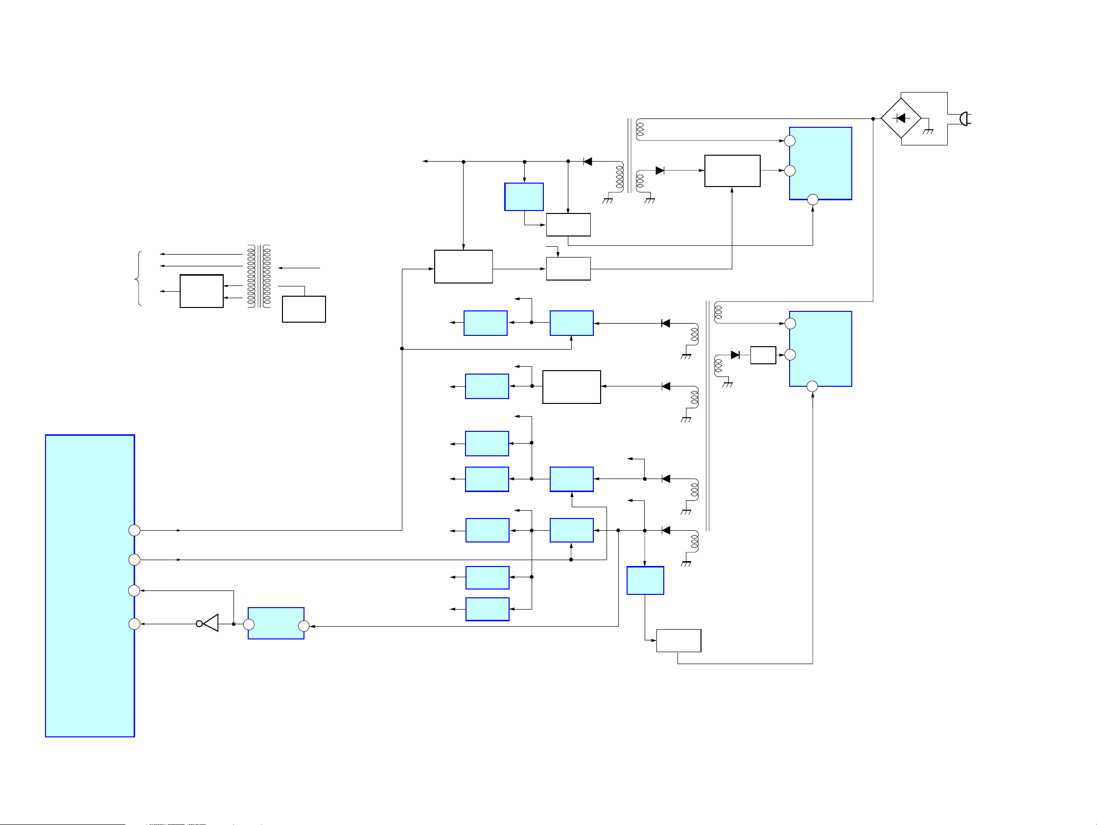
6-1. BLOCK DIAGRAM – RF/SERVO SECTION –
DETECTOR
OPTICAL PICK-UP
BLOCK
(KHM-310CAA)
LASER
DIODE
(FOR CD)
LASER
DIODE
(FOR DVD)
CD LD
DVD LD
WR650
VR780
PD
RF
DVDRFIP
6
OSP
252 253
OSN
• Signal Path
: CD PLAY
A
B
C
D
F
E
C
B
D
AUTOMATIC POWER
CONTROL (FOR CD)
AUTOMATIC POWER
CONTROL (FOR DVD)
VOLUME CONTROL
A
Q102 (1/2)
Q102 (2/2)
Q101, Q103
A
B
D
C
2
3
4
5
19
18
8
9
10
11
176
23
20
21
22
187
DVDA
DVDB
DVDC
DVDD
TPI
TNI
NA
NB
MD
MC
LI M SW
LD01
MD12
MD11
LD02
MSW
IC102 (1/3)
CD/DVD RF AMP,
FOCUS/TRACKING ERROR AMP
DVD SYSTEM PROCESSOR
DIGITAL SERVO PROCESSOR
PRST
IFCK
MAMUTE
IFSDO
IFSDI
XIFCS
110
99
51
98
101
100
43
MTK_XRST
33
DVD_SCO/CLK1
25
MAMUTE
32
DVD_SOD/RXD1
31
DVD_SID/TXD1
39
DVD_XIFCS
: DVD PLAY
: SACD PLAY
2AXIS
DEVICE
FOCUS/
TRACKING
COIL
FCS+
FCS–
TRK+
TRK–
(SLED)
(SPINDLE)
MM
MM
+3.3V
SP+
SP–
SL–
SL+
FOCUS/TRACKING COIL DRIVER,
SPINDLE, SLED MOTOR DRIVER
42
41
36 48
37 1
32
35 3
34 4
VCC
32
31
30
29
27
28
47
46
IC201
BUFFER
FOCUS COIL
DRIVE
TRACKING COIL
DRIVE
SLED MOTOR
DRIVE
SLED MOTOR
DRIVE
SPINDLE MOTOR
DRIVE
BUFFER
177
OCSW
105
IFBSY
179
CKSW
15
43
10
13
16
17
40
45
19
20
22
21
25
22
24
V1P4
FOO
TRO
FMO
DMO
V1P4
FMO
FOO
DMO
TRO
39
TROPENPWN
38
FMO
42
FOO
37
DND
41
TRO
V REFO
30
186
FWD
185
REV
40
IOPMON
47
SPFG
184
MUTE123
183
MUTE
181
TSDM
34
DVD_IFBUSY/RST1
IC509 (1/4)
SYSTEM
CONTROLLER
OCSW1
CKSW1
LDM+
LDM-
S001(CHUK/TRAY DETECT)
MM
(LOADING)
HCD-DZ700FW
2222
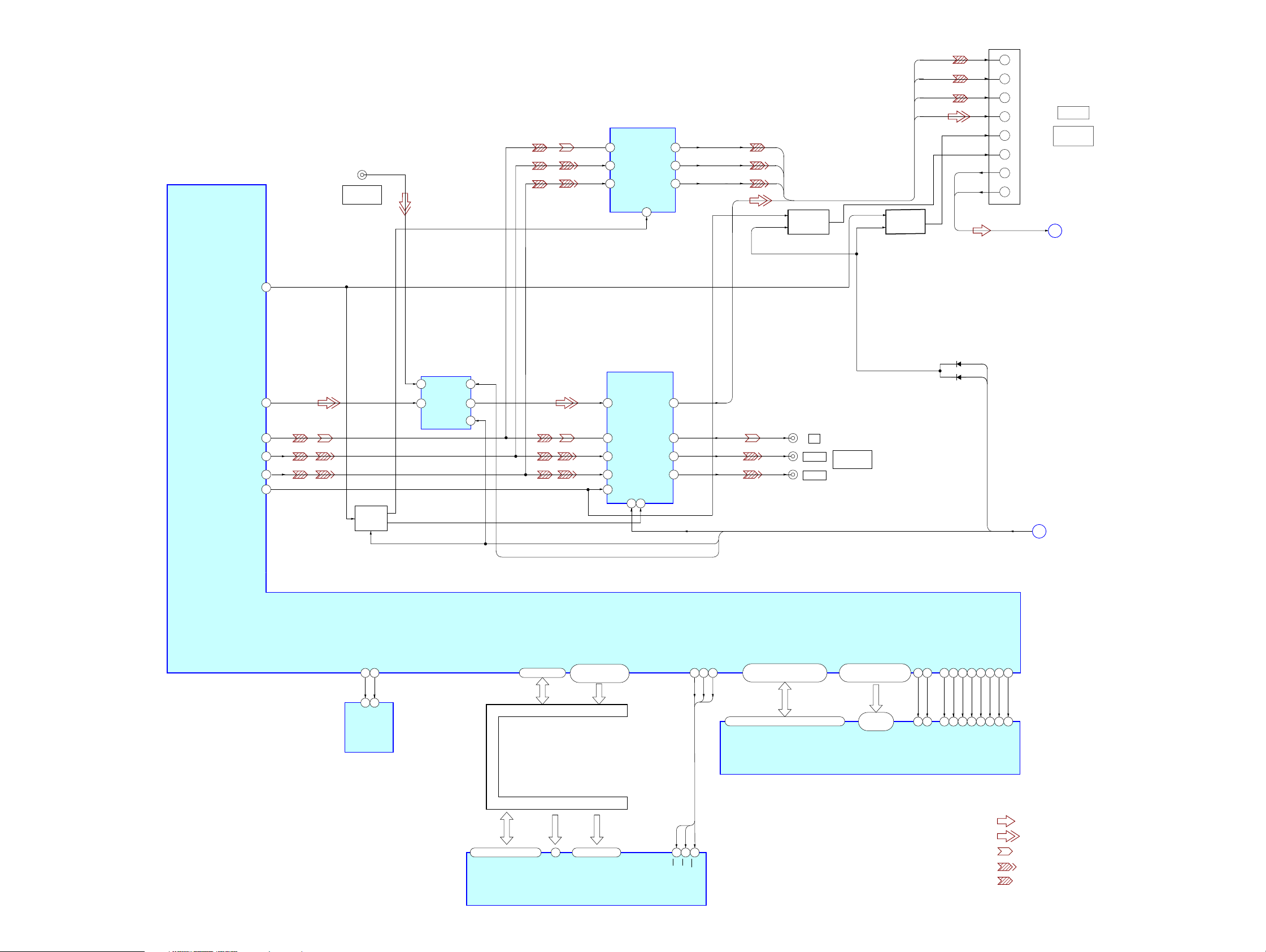
HCD-DZ700FW
6-2. BLOCK DIAGRAM – VIDEO SECTION –
169
RGB
198
YUY3
200
YUY4
202
YUY5
203
YUV6
171
WODE
J203(1/2)
SAT
VIDEO IN
Q207-209
MUTE
CONTROL
3
5
IC203
SELECTOR
IN2
IN3
SW1
OUT
SW2
CROUT
CYOUT
CBOUT
Q201-203
BLANKOUT
SWITCH
VOUT
D203
D202
L
R
AV SEL0
AV SEL1
IC202
VIDEO AMP, 75ohm DRIVER
VOUT
CYOUT
CBOUT
CROUT
AV SEL0
AV SEL1
AV SEL2
CYOUT
CBOUT
CROUT
WIDE
DVD SEL DVD SEL
Q204-206
FUNCTION
SWITCH
Y
PB/C
PR/C
B
R
RGB SEL
J203
COMPONENT
VIDEO OUT
11
CYIN
13
CBIN
15
CRIN
IC201
VIDEO AMP, 75Ω DRIVER
2
6
11
13
15
2
CVBSIN
CYIN
CBIN
CRIN
SI
MUTE1
5
14
7
4
CYOUT
CBOUTB
CROUTB
MUTE2
14
VOUT
CYOUT
CBOUT
CROUT
MUTE2
24
21
18
30
24
21
18
15
11
7
19
16
8
6
2
J202
AV SEL0-2
R/C OUT
G OUT
B OUT
V/Y OUT
BLANK
OUT
FUNCTION
SW
A(L) IN
A(R) IN
L, R
B
EURO AV
OUTPUT
(TO TV)
C
(Page 24)
AMP
SECTION
(Page 24)
AMP
SECTION
HCD-DZ700FW
SCL
102
103
6 5
SCL
IC103
EEPROM
SDA
SPA
IC102(2/3)
DVD SYSTEM PROCESSOR
AB0 – AB7
81-84,86-88,91
HD0 – HD7 A0 – A21
DATA & ADDRESS BUS
DATA & ADDRESS BUS
HD0 – HD7
29,31,33,35,38,40,42,44 25-16, 9-1, 48
DQ0 – DQ7
HIGHA0-7
IOA0-7, IOA18-IOA20
A16, A17
53-61, 67-72, 74-76,
78, 89, 92, 93
A0
A0 – A19DQ15/A-1
IC101
FLASH ROM
A1-A20
RA0 – RA11
146, 147, 149-151,
158-160, 162, 164-166
22-26,
29-35
RA0 – RA11
IC104
SDRAM
RCLK
RCS
RWE
MRAS
BA0
BA1
143
142
145 156 113 137 157
38
20
21
BS0
BS1
DRCLK
CAS
138
140
139
19
16
18
17
CAS
RCS
RAS
RWE
MDQM0
15
DQM0
MDQM1
39
DQM1
CLE
37
DRCLE
77
CEWEOE
IOCS
IOWA
IOUE
79
66
125-123, 121, 120, 118,
117, 115, 135, 133-128, 126
2,4,5,7,8,10,11,13,42,44,45,47,48,50,51,53
RD0 – RD15
RD0 – RD15
• Signal Path
: AUDIO
CE
OE
WE
2645
28OE11
CE
WE
: VIDEO
: Y
: COMPONENT VIDEO
: R, G, B
2323
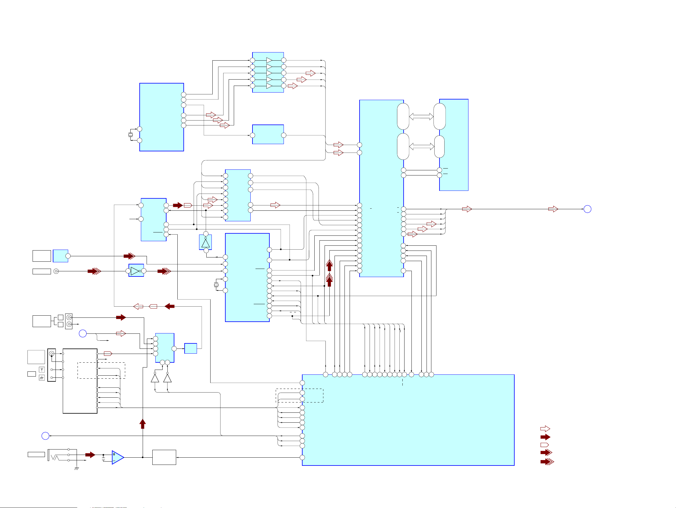
HCD-DZ700FW
6-3. BLOCK DIAGRAM – AMP SECTION –
X101
27MHz
R-CH
IC604
OPTICAL
IN
OPTICAL
DIGITAL IN
COAXIAL IN
AUDIO IN
COAXIAL
FM
75Ω
AM
VIDEO
SECTION
(Page 23)
J603
AUDIO IN
SAT
B
1
OUT
J602
J203(2/2)
L
R
VIDEO
SECTION
(Page 23)
FM/AM TUNER UNIT
FM ANT
GND
AM ANT
GND
AVSEL0-AVSEL2
R-CH
C
L-CH
R-CH
RDS-CLK
RDS-DATA
TUNED
R-CH
DO
CK
CE
DI
R-CH
R-CH
RDS-CLK
RDS-DATA
TUDI
TUDO
TUCLK
TCE
TUNED
5
6
IC605
2
AEP, UK
7
AMP
229
XTALI
228
XTALO
DVD SYSTEM PROCESSOR
IC501
A/D CONVERTER
1
LIN
2
RIN
4
IC608
INVERTER
Q603
IC102(3/3)
DOUT
SCKI
LRCK
BCK
PDWN
AUDIO INPUT
SELECTOR
15
X2
12
X
11
X3
14
X1
AV
SEL0
Q601,605
CONTROL
IC602
AB
10 9
AV
MUTE
ALRCK
ABCK
ACLK
ASDATA0
ASDATA1
ASDATA2
12
15
10
11
7
X
Q604
SEL2
IC4501
BUFFER
72
75
76
78
80
77
79
85
81
82
83
LRCK0
BCK0
D1
D2
D3
MCK0
DIR_CLK
DIR_RERR
AD RST
RDS_CLK
RDS_DATA
PLL_DO
PLL_DI
PLL_CLK
PLL_CE
TUNED
AV select0
AV select1
AV select2
DIN
38
SEL1 FS
65
60 5963
DSP PM
DSP XRST
D2
D3
DSP BST
DSP GP9
114
SDI3
115
SDI4
30
SD12
22
KFSIO
17
BCKI1
29
BCKI2
28
LRCK12
15
LRCK11
69
GP8
59
EXLOCK
33
HDIN
18
SDI1
2
XRST
113
PM
56
BS T
68
G9
DIN
5
DSP DIN/DIR DIN
IC506
DIGITAL AUDIO
PROCESSOR
DIR_CLK
DIR_HCE
DIR_HDOUT
70
7
67
DIR HCE
DIR HDOUT
DSP DIN/DIR CLK
72-75
77-80
D0-D15
98,99
102-105
107,108
64-66
82-85
A0-A15
92-97
109,110
WEO
CS0
LRCKO
BCKO
SCKOUT
SD01
SD02
SD03
HCLK
GP12
HCS
HD OUT
HACN
XSTATE
CSFLAG
DIR_RST
DIR_RERR
69
66
19
68
DIR RST
DIR UGPI
DIR CSFLAG
SYSTEM CONTROLLER
112
45 17
44 6
6
61
DSP HCE
DSP DOUT
LRCKO
BCKO
71
DSP SKIP
19
20
14
23
24
25
34
37
36
35
32
DIR_ZERO
58
18
DIR RERR
DIR ZORO
IC509 (2/4)
DSP ACK
7-10
13-16
18-21
24,25
29+32
35-38
5-1
44-42
27-24
21-19
SCK
D1
D3
D2
SD-RAM
D0 – D15
D0 – D15
WE
CS
IC507
D1 - D3, SCK,
BCKO, LRCKO
A
AUDIO
SECTION
(Page 25)
• R-CH is omitted due to same as L-CH.
• Signal Path
: AUDIO
: AUDIO IN
: TUNER
14
15
24
34
17
36
35
38
37
25
48
16
15
14
11
12
13
Y
4
XSTATE
DIR_HDOUT
DIR_CLK
DIR_HCE
CS FLAG
DIR_RST
DIR_ZORO
AEP, UK
RDS_CLK
RDS_DATA
TUDO
TUDI
TUCLK
TCE
TUNED
AV SEL0
AV SEL1
AV SEL2
5
6
9
8
7
213
214
215
217
218
219
IC514
SELECTOR
LRCK0
10 1
3B A/B
11
3A
2B
2A
1B
1A
4A
4B
XIN
DIGITAL AUDIO
XOUT
3Y
2Y
1Y
4Y
IC505
INTERFACE
BCKO
6
5
D1
3
2
14
MCK0
13
AMP
4
2
X500
12.288MHz
13 CKOUT
4DIN1
5DIN2
22
21
IC517
INVERTER
IC603
13
9
7
4
12
2
AUDIO
ERROR
XSTATE
CFALAG
A
LRCK
DATA
BCK
DI
DO
CL
CE
IC4502
BUFFER
: DIGITAL IN(OPTICAL IN)
IPOD/MICSW
91
: DIGITAL IN(COAXIAL IN)
HCD-DZ700FW
2424
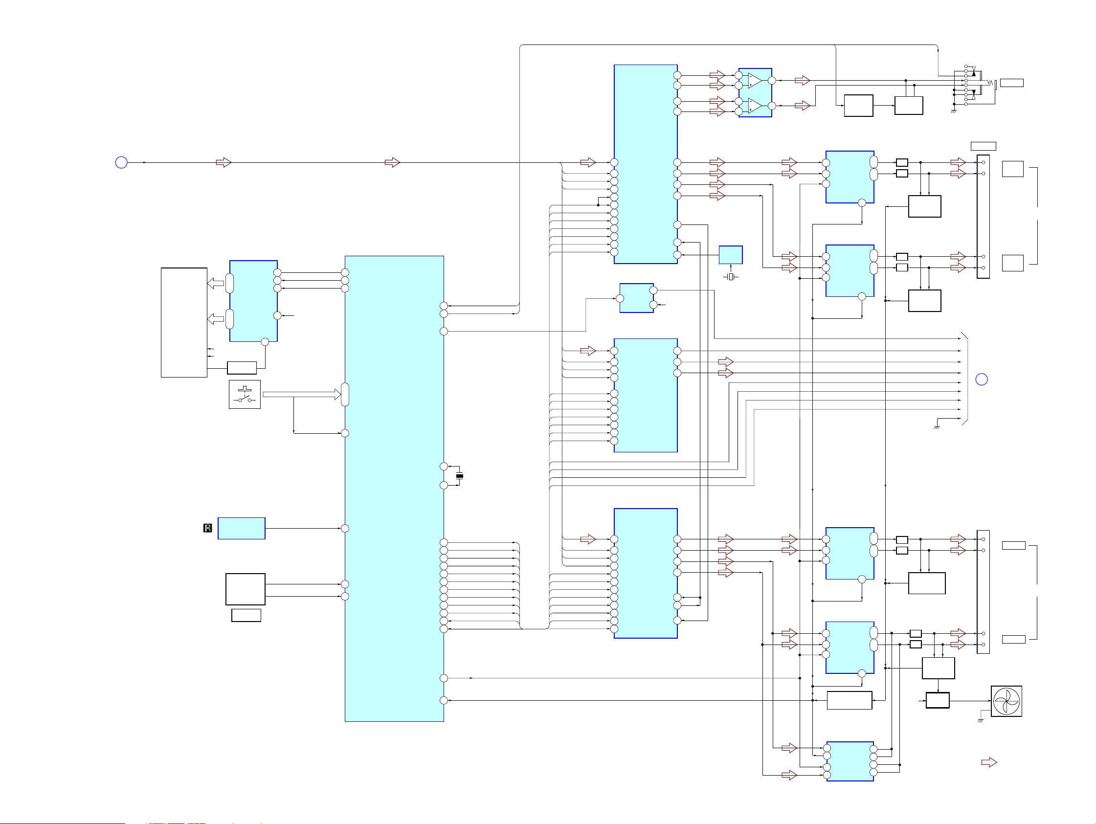
HCD-DZ700FW
6-4. BLOCK DIAGRAM – AUDIO SECTION –
D1 – D3, SCK,
AMP
SECTION
(Page 24)
BCKO, LRCKO
A
FL801
FLUORESCENT
INDICATOR TUBE
F1
F2
G1
S801 – S808
FL DRIVER
14 – 29
SG1 – SG16
47 – 31
GR2 – GR12
Q802
FL DRIVER
IC802
DIN
CLK
STB
42
GR1
R
R
L
L
IC305
OSC
X450
IC301
HEADPHONE
AMP
2
3
6
5
Q101, 102
DC
DETECT
Q103, 104
DC
DETECT
HP-SW
CSOD
BCKO
LRCKO
D2(SL/SR)
SDATA
SCLK
XLAT
XRST
D-GND
SPEAKER
Y
J801
PHONES
(+)
FRONT
R
(–)
(+)
FRONT
L
(–)
DIAT TRANSMIT
SECTION
(Page 27)
J203
1
7
HP-MUTE
POWER DRIVER
2
PWMBP
17
PWMAP
RESET
4
POWER DRIVER
2
PWMBP
17
PWMAP
RESET
4
Q507
MUTING
CONTROL
IC101
OUTB
OUTA
IC102
OUTB
OUTA
Q806 - 809
MUTING
29
LPF
30
25
LPF
26
SD
13
29
LPF
30
25
LPF
26
SD
13
IC108
STREAM PROCESSOR
45
HPOUTL1
43
HPOUTL2
41
HPOUTR1
39
HPOUTR2
D1
SCK
BCKO
LRCKO
OVF2
SCDT
SHIFT
LAT1
INIT
IC509 (3/4)
SYSTEM CONTROLLER
7
8
9
30
VFL
KEY0
27
24
28
97,95,94
74
FL DATA
FL CLK
FL CS/STB
KEY0 – KEY2
KEY INT
HP SW
HP MUTE
DIAT_CSOD
56
57
23
HP-SW
HP-MUTE
NSPMUTE
SOFTMUTE
D2
SCK
BCKO
LRCKO
MODEO
XRST
LINK
LAT2
INIT
NSPMUTE
SOFTMUTE
31
DATA
36
XFSIIN
30
BCK
29
LRCK
25
FLAGL OVF
24
OVF FLAGR
21
SCDT
22
SCSHIFT
23
SCLATCH
27
INIT
18
NSPMUTE
19
SOFTMUTE
IC502
INVERTER
B
4
Y
A
IC513
STREAM PROCESSOR
4
SDIN
2
RCK1
5
BCK1
6
LRCK1
26
MODEO
13
RST
14
MUTE
23
SCLATCH
27
INIT
18
NSPMUTE
19
SOFTMUTE
OUTR1
OUTR2
OUTL1
OUTL2
XFS0OUT
FS0I
XFS0IN
2
1
BCKO
LRCKO
SDOUT
6
4
11
9
14
38
48
49.152MHz
+3.3V
25
24
23
IC801
REMOTE CONTROL
RECEIVER
S800
VOLUME
ENCODER
VOLUME
4
10
11
SIRCS–IN
ENA
ENB
Xout
MODEO
XSCEN
M-ST/WMUTE
DAMP SCDT
DAMP SHIFT
DAMP LAT1
XRST
DAMP LAT3
DAMP INIT
DAMP SOFT MUTE
OVERFLOW1
OVERFLOW2
DRIVE RST
DRIVE OCP
SCDT
13
X502
Xin
5MHz
15
73
3
100
1
2
51
21
53
54
55
49
50
47
48
MODEO
XSCEN
LINK
SCDT
SHIFT
LAT1
XRST
LAT3
INIT
SOFTMUTE
OVF
OVF2
SHIFT
XSCEN
XRST
D3
SCK
BCKO
LRCKO
OVF
SCDT
SHIFT
LAT3
INIT
NSPMUTE
SOFTMUTE
OVF2
IC110
STREAM PROCESSOR
31
DATA
36
XFSIIN
30
BCK
29
LRCK
25
FLAGL OVF
21
SCDT
22
SCSHIFT
23
SCLATCH
27
INIT
18
NSPMUTE
SOFTMUTE
19
OVF FLAGR
24
OUTR1
OUTR2
OUTL1
OUTL2
FS0I
FS0CKO
XFS0IN
IC105
POWER DRIVER
6
4
11
9
38
37
48
C
C
WF
WF
2
PWMBP
17
PWMAP
RESET
4
POWER DRIVER
2
PWMBP
17
PWMAP
RESET
4
PROTECT DETECT
POWER DRIVER
2
PWMBP
13
SD
4
RESET
17
PWMAP
IC106
Q301
IC107
OUTB
OUTA
13
OUTB
OUTA
13
OUTB
OUTA
29
LPF
30
25
LPF
26
SD
29
30
25
26
SD
29
30
25
26
+12V
Q109, 110
DETECT
LPF
LPF
DC
Q111, 112
DC
DETECT
FAN
DRIVE
Q302-304
(+)
CENTER
(–)
(+)
WOOFER
(–)
FAN
• Signal Path
: AUDIO
J202
HCD-DZ700FW
2525
HCD-DZ700FW
6-5. BLOCK DIAGRAM – POWER SECTION –
TO FLUORESCENT
INDICATOR TUBE
VFL
T901
TRANSFORMER(MAIN)
IC901
3
D
4
8
4
VCC
FB/OLP
STARTUP
VCC
FB/OLP
POWER
PROTECTION
5
IC921
POWER
PROTECTION
6
D931
+31.5V
IC931
VOLTAGE
DETECT
DC/DC
CONVERTER
T801
F1
F2
+5V
RECT
Q943,947
VOLTAGE
DETECT
E4V
PC901
PHOTO
COUPLER
PC903
PHOTO
COUPLER
D801,802
IC515
+9V REG
IC516
+5V REG
+12V
IC941
+12V REG
M -8V
Q945
MOTER DRIVE
CONTROLLER
D804,805
OSC
Q801
+9V
+5V
D905
T902
TRANSFORMER (SUB)
D941
D944
Q901
VOLTAGE
CONTROLLER
D922
Q921
REG
D901
AC IN
IC509 (4/4)
SYSTEM CONTROLLER
+5V
+3.3V
RF +3.3V
44P CONT2
+1.8V
40P CONT1
+1.8V
20AC_CUT
Q506
12RESET
IC511
1
RESET
2
+2.5V
IC105
+3.3V REG
IC107
+3.3V REG
+3.3V
IC106
+1.8V REG
IC303
+1.8V REG
IC508
+2.5V REG
IC942
+5V REG
IC943
+3.3V REG
+6V
D942
E 4V
D943
IC951
VOLTAGE
DETECT
PC902
PHOTO
COUPLER
HCD-DZ700FW
2626
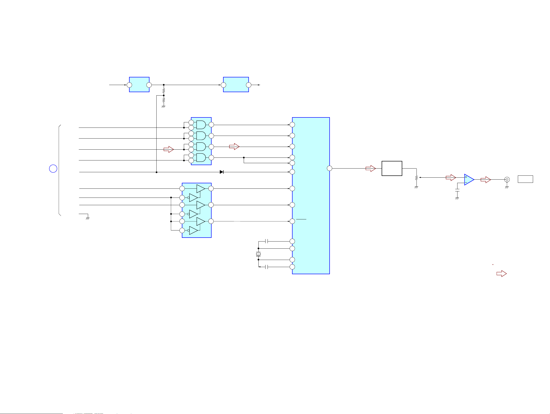
6-6. BLOCK DIAGRAM – DIAT TRANSMIT SECTION –
HCD-DZ700FW
AUDIO
SECTION
(Page 25)
Y
LRCKO
BCKO
D2(SL/SR)
XRST
CSOD
SDATA
XLAT
SCLK
D-GND
+12V
IC800
REG
VCC(9V)
R835
R836
5
4
12
13
10
IC802
LEVEL SHIFT
4
5
10
9
13
12
1
2
6
8
11
3
D800
6
11
8
IC801
641 4
+2.5V REG
+2.5V
RF MODULATOR
D/A CONVERTER
49
LRCK
50
BCK
48
DTIN
41
APS
64
XRST
16
CSOD
15
SWDT
13
SCLK
14
XSCEN
IC804
DAAOUT
21
Q801
BUFFER
RV801
IC805
RF AMP
3
4
C842
1
J801
DIR-T1
9
LEVEL SHIFT
IC803
X801
24.576MHz
C820
C819
54
57
59
60
C SST
O SCI
OSCO
XTCK4
Signal Path
: AUDIO
HCD-DZ700FW
2727
 Loading...