

Page 1
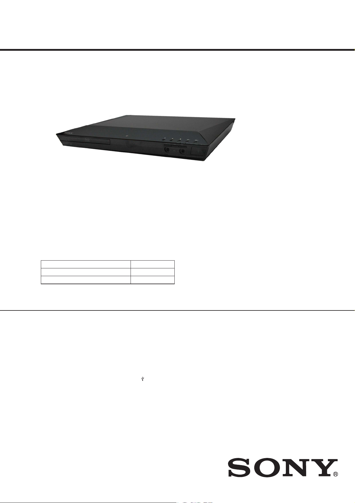
HBD-E2100/E3100/E3200/E4100/
E6100
SERVICE MANUAL
Ver. 1.7 2014.06
Photo: HBD-E3100
• HBD-E2100 is the amplifi er, video, HDMI, BD/DVD/CD system, USB, LAN,
wireless LAN, Bluetooth, NFC and FM tuner section in BDV-E2100.
• HBD-E3100 is the amplifi er, video, HDMI, BD/DVD/CD system, USB, LAN,
wireless LAN, Bluetooth, NFC and FM tuner section in BDV-E3100.
• HBD-E3200 is the amplifier, video, HDMI, BD/DVD/CD system, USB, LAN,
wireless LAN, Bluetooth, NFC and FM tuner section in BDV-E3200.
• HBD-E4100 is the amplifi er, video, HDMI, BD/DVD/CD system, USB, LAN,
wireless LAN, Bluetooth, NFC and FM tuner section in BDV-E4100.
• HBD-E6100 is the amplifi er, video, HDMI, BD/DVD/CD system, USB, LAN,
wireless LAN, Bluetooth, NFC and FM tuner section in BDV-E6100.
US Model
HBD-E2100/E3100
Canadian Model
Singapore Model
HBD-E2100/E3100/E4100/E6100
AEP Model
Taiwan Model
HBD-E2100/E4100/E6100
UK Model
HBD-E2100/E3100/E4100
Chinese Model
HBD-E4100/E6100
E Model
HBD-E2100/E3100/E3200/E4100/E6100
Argentina Model
BDV-E2100/E4100
Australian Model
HBD-E2100/E6100
Russian Model
Saudi Arabia Model
Model Name Using Similar Mechanism BDP-S3100
Mechanism Type BPX-7
Optical Pick-up Block Name KEM480AAA
Amplifi er Section
US model only:
AUDIO POWER SPECIFICATIONS
POWER OUTPUT AND TOTAL HARMONIC DISTORTION:
(FTC)
Front L + Front R: With 3 ohms loads, both channels driven, from
180 Hz - 20,000 Hz;
rated 50 watts per channel
minimum RMS power, with no more than 1%
total harmonic distortion from 250 milliwatts to
rated output.
BDV-E6100/BDV-E4100/BDV-E3100/BDV-E3200
BDV-E2100 (Except UK model):
POWER OUTPUT (rated)
Front L/Front R: 75 W + 75 W (at 3 ohms, 1 kHz, 1% THD)
POWER OUTPUT (reference)
Front L/Front R/Surround L/Surround R:
125 W (per channel at 3 ohms, 1 kHz)
Center: 250 W (at 6 ohms, 1 kHz)
Subwoofer: 250 W (at 6 ohms, 80 Hz)
Inputs (Analog)
AUDIO IN Sensitivity: 1 V/400 mV
MIC 1/2 Sensitivity: 10 mV (Singapore model)
Inputs (Digital)
TV (Audio Return Channel/OPTICAL)
Supported formats: LPCM 2CH
(up to 48 kHz), Dolby Digital, DTS
BDV-E2100 (UK model)
POWER OUTPUT (rated)
Front L/Front R: 75 W + 75 W (at 3 ohms, 1 kHz, 1% THD)
POWER OUTPUT (reference)
Front L/Front R/Surround L/Surround R:
100 W (per channel at 3 ohms, 1 kHz)
Center: 200 W (at 6 ohms, 1 kHz)
Subwoofer: 200 W (at 6 ohms, 80 Hz)
BDV-E4100/ BDV-E6100 (Chinese model)
POWER OUTPUT
Front L/Front R/Surround L/Surround R:
75 W (per channel at 3 ohms, 1 kHz)
Center: 150 W (at 6 ohms, 1 kHz)
Subwoofer: 150 W (at 6 ohms, 80 Hz)
Inputs (Analog)
AUDIO IN Sensitivity: 1 V/400 mV
Inputs (Digital)
TV (Audio Return Channel/OPTICAL)
Supported formats: LPCM 2CH (up to 48 kHz),
Dolby Digital, DTS
HDMI Section
Connector Type A (19 pin)
BD/DVD/CD System
Signal format system NTSC/PAL (except US, PX and Canadian models)
NTSC (US, PX and Canadian models)
USB Section
(USB) port: Type A (For connecting USB memory, memory
card reader, digital still camera, and digital video
camera)
LAN Section
LAN (100) terminal 100 BASE-TX Terminal
Wireless LAN Section
Standards Compliance IEEE 802.11 b/g/n
Frequency and Channel US, Canadian, Argentina and Taiwan models:
2.4 GHz band: channels 1–11
Other models:
2.4 GHz band: channels 1–13
Frequency band 2.4000 GHz - 2.4835 GHz
9-890-611-08
2014F80-1
2014.06
©
Sony Corporation
Published by Sony EMCS (Malaysia) PG Tec
SPECIFICATIONS
Thai Model
HBD-E3100/E4100/E6100
South African Model
HBD-E2100/E3100/E6100
PX Model
HBD-E2100
Bluetooth Section
Communication system Bluetooth Specification version 3.0
Output Bluetooth Specification Power Class 2
Maximum communication range
Line of sight approx. 10 m
(except US, PX and Canadian models)
Line of sight approx. 10 m (33ft)
(US, PX and Canadian models)
Frequency band 2.4 GHz band
2.4000 GHz - 2.4835 GHz
Modulation method FHSS (Freq Hopping Spread Spectrum)
Compatible Bluetooth profiles
Supported Codecs3) SBC4), AAC
Transmission range (A2DP)
20 Hz – 20,000 Hz (Sampling frequency
44.1 kHz, 48 kHz)
1)
The actual range will vary depending on factors such as obstacles
between devices, magnetic fields around a microwave oven, static
electricity, cordless phone, reception sensitivity, antenna’s perfor mance, operating system, software application, etc.
2)
Bluetooth standard profiles indicate the purpose of Bluetooth
communication between devices.
3)
Codec: Audio signal compression and conversion format
4)
Subband Codec
2)
A2DP 1.2 (Advanced Audio Distribution
Profile)
AVRCP 1.3 (Audio Video Remote Control
Profile)
1)
1)
BLU-RAY DISC/DVD RECEIVER
Page 2
HBD-E2100/E3100/E3200/E4100/E6100
Ver. 1.5
FM Tuner Section
System PLL quartz-locked digital synthesizer
Tuning range 87.5 MHz - 108.0 MHz (50 kHz step)
(except US, PX and Canadian models)
87.5 MHz - 108.0 MHz (100 kHz step)
(US, PX and Canadian models)
Antenna (aerial) FM wire antenna (aerial)
General
Power requirements US and Canadian models:
120 VAC, 60 Hz
Taiwan model:
120 V AC, 50/60 Hz
Latin-American, 110 – 240 V AC area in
E model and PX models:
110 V – 240 V AC, 50/60 Hz
Saudi Arabia model:
127 V – 240 V AC, 50/60 Hz
Other models:
220 V – 240 V AC, 50/60 Hz
Power consumption On: 95 W
Standby: 0.3 W
Dimensions (w/h/d) (approx.)
430 mm × 50.5 mm × 296 mm
(17 in × 2 in × 11
Mass (approx.) 2.7 kg (5 lb 16 oz)
Design and specifications are subject to change without notice.
• Standby power consumption: 0.3 W.
• Over 85% power efficiency of amplifier block is achieved with the full digital amplifier, S-Master.
• This system incorporates with Dolby* Digital and Dolby Pro Logic adaptive matrix surround
decoder and the DTS** Digital Surround System.
* Manufactured under license from Dolby Laboratories.
Dolby, Pro Logic, and the double-D symbol are trademarks of Dolby Laboratories.
** Manufactured under license under U.S. Patent Nos: 5,956,674; 5,974,380; 6,226,616;
6,487,535; 7,212,872; 7,333,929; 7,392,195; 7,272,567 & other U.S. and worldwide patents
issued & pending. DTS-HD, the Symbol, & DTS-HD and the Symbol together are registered trademarks of DTS, Inc. Product includes software. © DTS, Inc. All Rights Reserved.
• This system incorporates High-Defi nition Multimedia Interface (HDMI
The terms HDMI and HDMI High-Defi nition Multimedia Interface, and the HDMI Logo are
trademarks or registered trademarks of HDMI Licensing LLC in the United States and other
countries.
• Java is a trademark of Oracle and/or its affi liates.
• “DVD logo” is a trademark of DVD Format/ Logo Licensing Corporation.
• “Blu-ray Disc”, “Blu-ray”, “Blu-ray 3D”, “BD-LIVE”, “BONUSVIEW”, and logos are trademarks of the Blu-ray Disc Association.
• “Blu-ray Disc”, “DVD+RW”, “DVD-RW”, “DVD+R”, “DVD-R”, “DVD VIDEO”, and “CD”
logos are trademarks.
• “BRAVIA” is a trademark of Sony Corporation.
• “AVCHD 3D/Progressive” and the “AVCHD 3D/Progressive” logo are trademarks of Panasonic
Corporation and Sony Corporation.
, “XMB”, and “xross media bar” are trademarks of Sony Corporation and Sony Computer
•
Entertainment Inc.
• “Playstation” is a registered trademark of Sony Computer Entertainment Inc.
• “Sony Entertainment Network logo” and “Sony Entertainment Network” are trademarks of Sony
Corporation.
• Music and video recognition technology and related data are provided by Gracenote®.
Gracenote is the industry standard in music recognition technology and related content delivery.
For more information, please visit www.gracenote.com.
CD, DVD, Blu-ray Disc, and music and video-related data from Gracenote, Inc., copyright ©
2000-present Gracenote.
Gracenote Software, copyright © 2000-present Gracenote. One or more patents owned by Gra-
cenote apply to this product and service. See the Gracenote website for a nonexhaustive list of
applicable Gracenote patents. Gracenote, CDDB, MusicID, MediaVOCS, the Gracenote logo
and logotype, and the “Powered by Gracenote” logo are either registered trademarks or trademarks of Gracenote, Inc. in the United States and/or other countries.
• Wi-Fi®, Wi-Fi Protected Access® and Wi-Fi Alliance® are registered marks of the Wi-Fi
Alliance.
• Wi-Fi CERTIFIED™, WPA™, WPA2™ and Wi-Fi Protected Setup™ are marks of the Wi-Fi
Alliance.
• The N Mark is a trademark or registered trademark of NFC Forum, Inc. in the United States and
in other countries.
• Android is a trademark of Google Inc.
• The Bluetooth
and any use of such marks by Sony Corporation is under license. Other trademarks and trade
names are those of their respective owners.
• MPEG Layer-3 audio coding technology and patents licensed from Fraunhofer IIS and
Thomson.
• This product incorporates proprietary technology under license from Verance Corporation and
is protected by U.S. Patent 7,369,677 and other U.S. and worldwide patents issued and pending
as well as copyright and trade secret protection for certain aspects of such technology. Cinavia
is a trademark of Verance Corporation. Copyright 2004-2010 Verance Corporation. All rights
reserved by Verance. Reverse engineering or disassembly is prohibited.
®
word mark and logos are registered trademarks owned by Bluetooth SIG, Inc.
¾ in) incl. projecting parts
TM
) technology.
SAFETY-RELATED COMPONENT WARNING!
COMPONENTS IDENTIFIED BY MARK 0 OR DOTTED LINE
WITH MARK 0 ON THE SCHEMATIC DIAGRAMS AND IN
THE PARTS LIST ARE CRITICAL TO SAFE OPERATION.
REPLACE THESE COMPONENTS WITH SONY PARTS
WHOSE PART NUMBERS APPEAR AS SHOWN IN THIS
MANUAL OR IN SUPPLEMENTS PUBLISHED BY SONY.
• Windows Media is either a registered trademark or trademark of Microsoft Corporation in the
United States and/or other countries.
This product is protected by certain intellectual property rights of Microsoft Corporation. Use
or distribution of such technology outside of this product is prohibited without a license from
Microsoft or an authorized Microsoft subsidiary.
Content owners use Microsoft
tellectual property, including copyrighted content. This device uses PlayReady technology to
access PlayReady-protected content and/or WMDRM-protected content. If the device fails to
properly enforce restrictions on content usage, content owners may require Microsoft to revoke
the device’s ability to consume PlayReady-protected content. Revocation should not affect unprotected content or content protected by other content access technologies. Content owners may
require you to upgrade PlayReady to access their content. If you decline an upgrade, you will not
be able to access content that requires the upgrade.
• DLNA™, the DLNA Logo and DLNA CERTIFIED™ are trademarks, service marks, or certifi -
cation marks of the Digital Living Network Alliance.
• Opera® Devices SDK from Opera Software ASA. Copyright 1995-2013 Opera Software ASA.
All rights reserved.
• All other trademarks are trademarks of their respective owners.
• Other system and product names are generally trademarks or registered trademarks of the manufacturers. ™ and ® marks are not indicated in this document.
®
PlayReady™ content access technology to protect their in-
End User License Information
Gracenote® End User License Agreement
This application or device contains software from Gracenote, Inc. of Emeryville, California
(“Gracenote”). The software from Gracenote (the “Gracenote Software”) enables this application
to perform disc and/or fi le identifi cation and obtain music-related information, including name,
artist, track, and title information (“Gracenote Data”) from online servers or embedded databases
(collectively, “Gracenote Servers”) and to perform other functions. You may use Gracenote Data
only by means of the intended End-User functions of this application or device.
You agree that you will use Gracenote Data, the Gracenote Software, and Gracenote Servers for
your own personal non-commercial use only. You agree not to assign, copy, transfer or transmit
the Gracenote Software or any Gracenote Data to any third party. YOU AGREE NOT TO USE
OR EXPLOIT GRACENOTE DATA, THE GRACENOTE SOFTWARE, OR GRACENOTE
SERVERS, EXCEPT AS EXPRESSLY PERMITTED HEREIN.
You agree that your non-exclusive license to use the Gracenote Data, the Gracenote Software,
and Gracenote Servers will terminate if you violate these restrictions. If your license terminates,
you agree to cease any and all use of the Gracenote Data, the Gracenote Software, and Gracenote
Servers. Gracenote reserves all rights in Gracenote Data, the Gracenote Software, and the Gracenote
Servers, including all ownership rights. Under no circumstances will Gracenote become liable for
any payment to you for any information that you provide. You agree that Gracenote, Inc. may enforce
its rights under this Agreement against you directly in its own name.
The Gracenote service uses a unique identifi er to track queries for statistical purposes. The purpose
of a randomly assigned numeric identifi er is to allow the Gracenote service to count queries without
knowing anything about who you are. For more information, see the web page for the Gracenote
Privacy Policy for the Gracenote service.
The Gracenote Software and each item of Gracenote Data are licensed to you “AS IS.” Gracenote
makes no representations or warranties, express or implied, regarding the accuracy of any Gracenote
Data from in the Gracenote Servers. Gracenote reserves the right to delete data from the
Gracenote Servers or to change data categories for any cause that Gracenote deems suffi cient.
No warranty is made that the Gracenote Software or Gracenote Servers are error-free or that
functioning of Gracenote Software or Gracenote Servers will be uninterrupted. Gracenote is not
obligated to provide you with new enhanced or additional data types or categories that Gracenote
may provide in the future and is free to discontinue its services at any time. GRACENOTE
DISCLAIMS ALL WARRANTIES EXPRESS OR IMPLIED, INCLUDING, BUT NOT LIMITED
TO, IMPLIED WARRANTIES OF MERCHANTABILITY, FITNESS FOR A PARTICULAR
PURPOSE, TITLE, AND NON-INFRINGEMENT. GRACENOTE DOES NOT WARRANT THE
RESULTS THAT WILL BE OBTAINED BY YOUR USE OF THE GRACENOTE SOFTWARE
OR ANY GRACENOTE SERVER. IN NO CASE WILL GRACENOTE BE LIABLE FOR ANY
CONSEQUENTIAL OR INCIDENTAL DAMAGES OR FOR ANY LOST PROFITS OR LOST
REVENUES.
© Gracenote, Inc. 2009
CAUTION
Use of controls or adjustments or performance of procedures
other than those specifi ed herein may result in hazardous radia-
tion exposure.
ATTENTION AU COMPOSANT AYANT RAPPORT
LES COMPOSANTS IDENTIFIÉS PAR UNE MARQUE 0 SUR
LES DIAGRAMMES SCHÉMATIQUES ET LA LISTE DES
PIÈCES SONT CRITIQUES POUR LA SÉCURITÉ DE FONCTIONNEMENT. NE REMPLACER CES COMPOSANTS QUE
PAR DES PIÈCES SONY DONT LES NUMÉROS SONT DONNÉS DANS CE MANUEL OU DANS LES SUPPLÉMENTS
PUBLIÉS PAR SONY.
À LA SÉCURITÉ!
2
Page 3
SAFETY CHECK-OUT
After correcting the original service problem, perform the following safety check before releasing the set to the customer:
Check the antenna terminals, metal trim, “metallized” knobs,
screws, and all other exposed metal parts for AC leakage.
Check leakage as described below.
LEAKAGE TEST
The AC leakage from any exposed metal part to earth ground and
from all exposed metal parts to any exposed metal part having a
return to chassis, must not exceed 0.5 mA (500 microamperes.).
Leakage current can be measured by any one of three methods.
1. A commercial leakage tester, such as the Simpson 229 or RCA
WT-540A. Follow the manufacturers’ instructions to use these
instruments.
2. A battery-operated AC milliammeter. The Data Precision 245
digital multimeter is suitable for this job.
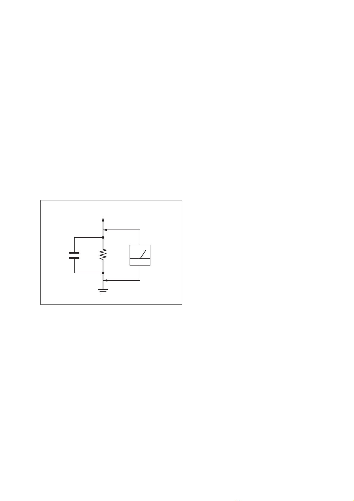
3. Measuring the voltage drop across a resistor by means of a
VOM or battery-operated AC voltmeter. The “limit” indication
is 0.75 V, so analog meters must have an accurate low-voltage
scale. The Simpson 250 and Sanwa SH-63Trd are examples
of a passive VOM that is suitable. Nearly all battery operated
digital multimeters that have a 2 V AC range are suitable. (See
Fig. A)
HBD-E2100/E3100/ E3200/E4100/E6100
Ver. 1.5
To Exposed Metal
Parts on Set
AC
1.5 kΩ0.15 μF
Earth Ground
Fig. A. Using an AC voltmeter to check AC leakage.
voltmeter
(0.75 V)
3
Page 4
HBD-E2100/E3100/E3200/E4100/E6100
Ver. 1.5
TABLE OF CONTENTS
1. SERVICING NOTES .............................................. 5
2. DISASSEMBLY
2-1. Disassembly Flow ........................................................... 13
2-2. How To Bend FFC .......................................................... 14
2-3. Case ................................................................................. 15
2-4. Panel Loading Assy ........................................................ 15
2-5. Front Panel Assy ............................................................. 16
2-6. BD Drive (BPX-7) .......................................................... 16
2-7. POWER KEY Board, WLAN/BT COMBO Card,
KARAOKE Board (SP, RU), PANEL Board .................. 17
2-8. MB1002 Board ............................................................... 18
2-9. AMP Board ..................................................................... 18
2-10. SWITCHING REGULATOR (SWR1) ........................... 19
2-11. Optical Pick-up Block (KEM480AAA),
Wire (Flat Type) .............................................................. 20
3. TEST MODE ............................................................. 21
4. ELECTRICAL CHECK .......................................... 32
5. TROUBLESHOOTING ........................................... 33
6. DIAGRAMS
6-1. Block Diagram - SERVO Section - ................................ 37
6-2. Block Diagram - MEMORY/HDMI Section - ................ 38
6-3. Block Diagram - MAIN Section - ................................... 39
6-4. Block Diagram - AMP Section - ..................................... 40
6-5. Block Diagram - POWER SUPPLY Section - ................ 41
6-6. Printed Wiring Board
- MB1002 Board (Component Side) - ............................ 43
6-7. Printed Wiring Board
- MB1002 Board (Conductor Side) - .............................. 44
6-8. Schematic Diagram - MB1002 Board (1/6) - ................. 45
6-9. Schematic Diagram - MB1002 Board (2/6) - ................. 46
6-10. Schematic Diagram - MB1002 Board (3/6) - ................. 47
6-11. Schematic Diagram - MB1002 Board (4/6) - ................. 48
6-12. Schematic Diagram - MB1002 Board (5/6) - ................. 49
6-13. Schematic Diagram - MB1002 Board (6/6) - ................. 50
6-14. Printed Wiring Board
- AMP Board (Component Side) - .................................. 51
6-15. Printed Wiring Board
- AMP Board (Conductor Side) - .................................... 52
6-16. Schematic Diagram - AMP Board (1/3) - ....................... 53
6-17. Schematic Diagram - AMP Board (2/3) - ....................... 54
6-18. Schematic Diagram - AMP Board (3/3) - ....................... 55
6-19. Printed Wiring Board - PANEL Board - ......................... 56
6-20. Schematic Diagram - PANEL Board - ............................ 57
6-21. Printed Wiring Board
- KARAOKE Board (SP, RU) - ...................................... 58
6-22. Schematic Diagram
- KARAOKE Board (SP, RU) - ...................................... 58
6-23. Printed Wiring Board - POWER KEY Board -............... 58
6-24. Schematic Diagram - POWER KEY Board - ................. 58
7. EXPLODED VIEWS
7-1. Case Section .................................................................... 76
7-2. Front Panel Section ......................................................... 77
7-3. Chassis Bottom Section .................................................. 78
7-4. Chassis Section ............................................................... 80
7-5. BD Drive Section (BPX-7) ............................................. 81
8. ELECTRICAL PARTS LIST .............................. 82
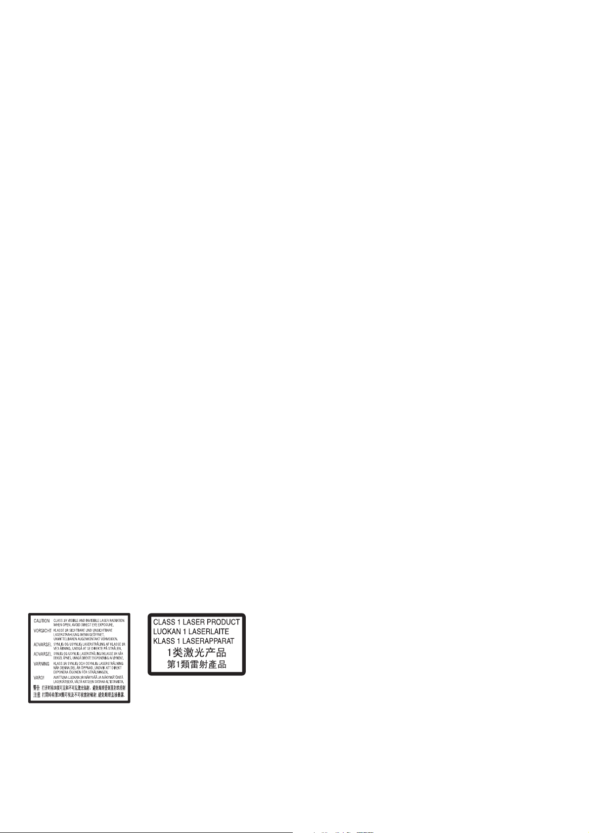
This appliance is classified as a
CLASS 3R LASER product.
Visible and invisible laser radiation
is emitted when the laser protective
housing is opened, so be sure to
avoid direct eye exposure.
This marking is located on the laser
protective housing inside the
enclosure.
4
This appliance is classified as a
CLASS 1 LASER product. This
marking is located on the rear
exterior.
The nameplate is located on the
bottom exterior.
NOTES ON CHIP COMPONENT REPLACEMENT
• Never reuse a disconnected chip component.
• Notice that the minus side of a tantalum capacitor may be dam-
aged by heat.
FLEXIBLE CIRCUIT BOARD REPAIRING
• Keep the temperature of soldering iron around 270 °C during
repairing.
• Do not touch the soldering iron on the same conductor of the
circuit board (within 3 times).
• Be careful not to apply force on the conductor when soldering
or unsoldering.
Page 5
HBD-E2100/E3100/E3200/E4100/E6100
SECTION 1
SERVICING NOTES
Ver. 1.5
NOTES ON HANDLING THE OPTICAL PICK-UP
BLOCK OR BASE UNIT
The laser diode in the optical pick-up block may suffer electrostatic break-down because of the potential difference generated by
the charged electrostatic load, etc. on clothing and the human body.
During repair, pay attention to electrostatic break-down and also
use the procedure in the printed matter which is included in the
repair parts.
The fl exible board is easily damaged and should be handled with
care.
NOTES ON LASER DIODE EMISSION CHECK
The laser beam on this model is concentrated so as to be focused
on the disc refl ective surface by the objective lens in the optical
pickup block. Therefore, when checking the laser diode emission,
observe from more than 30 cm away from the objective lens.
UNLEADED SOLDER
Boards requiring use of unleaded solder are printed with the leadfree mark (LF) indicating the solder contains no lead.
(Caution: Some printed circuit boards may not come printed with
the lead free mark due to their particular size)
: LEAD FREE MARK
Unleaded solder has the following characteristics.
• Unleaded solder melts at a temperature about 40 °C higher
than ordinary solder.
Ordinary soldering irons can be used but the iron tip has to be
applied to the solder joint for a slightly longer time.
Soldering irons using a temperature regulator should be set to
about 350 °C.
Caution: The printed pattern (copper foil) may peel away if
the heated tip is applied for too long, so be careful!
• Strong viscosity
Unleaded solder is more viscous (sticky, less prone to fl ow)
than ordinary solder so use caution not to let solder bridges
occur such as on IC pins, etc.
• Usable with ordinary solder
It is best to use only unleaded solder but unleaded solder may
also be added to ordinary solder.
RELEASING THE DISC TRAY LOCK
The disc tray lock function for the antitheft of an demonstration
disc in the store is equipped.
Releasing Procedure:
1. Press the [
2. Touch the [FUNCTION] sensor to select “BD/DVD”.
3. Touch the [x] and [Z] sensors simultaneously and hold down
until “D. OFF” displayed on the fluorescent indicator tube
(around 5 seconds).
Note: When “D. LOCK” is displayed, the disc tray lock is not released by
turning power on/off with the [
ABOUT THE LENS CLEANING
Do not do the lens cleaning with the cotton bud etc. It causes the
trouble.
] button to turn on the system.
?/1
] button.
?/1
NOTE OF REPLACING THE IC101, IC102, IC103,
IC203, IC204, IC601, IC706, IC801 AND IC1001 ON
THE MB1002 BOARD
IC101, IC102, IC103, IC203, IC204, IC601, IC706, IC801 and
IC1001 on the MB1002 board cannot exchange with single. When
these parts on the MB1002 board are damaged, exchange the entire
mounted board.
NOTE OF REPLACING THE IC102 AND IC103 ON
THE MB1002 BOARD
Replacement of IC102 and IC103 on the MB1002 board used in
this unit requires a special tool.
TEST DISC
Part No. Description Layer
J-6090-199-A BLX-104 Single Layer
J-6090-200-A BLX-204 Dual Layer
J-2501-307-A CD (HLX-A1)
J-2501-305-A HLX-513 Single Layer (NTSC)
J-2501-306-A HLX-514 Dual Layer (NTSC)
J-6090-077-A HLX-506 Single Layer (PAL)
J-6090-078-A HLX-507 Dual Layer (PAL)
Note: Refer to the service manual of BDP-BX1/S350 (Part No. 9-883-
989-1[]) (page 1-3 to 1-14E) for the use of BLX-104/204.
Operation and Display:
1. BLX-104
Procedure:
1. Select 23.976Hz/1080p.
2. Play “4.Motion picture”.
3. Check whether player can play back or not.
4. Check each outputs.
Video:
Composite/S Video/component/HDMI.
Audio:
Speaker out.
* When 1080/24p monitor is nothing, 1080i (59.94Hz or 50Hz)
can use instead of 1080/24p.
However this is temporary correspondence.
2. BLX-204
Procedure:
1. Select 1080i (59.94Hz or 50Hz).
2. Play “4.Motion picture”.
3. Check whether player can play back or not (Check the picture
and sound output).
3. CD (HLX-A1)
Procedure:
Check whether player can play back or not (Check the sound output).
4. HLX-513/514 (NTSC), HLX-506/507 (PAL)
Procedure:
1. After displayed Main Menu, select “1.Video Signal”.
2. Play “1.Color bar 100%” (Check the picture and sound output).
3. Return to Menu.
4. Play “Demonstration 4:3” or “Demonstration 16:9” (Check the
picture and sound output).
5
Page 6

HBD-E2100/E3100/E3200/E4100/E6100
Ver. 1.5
NOTE OF REPLACING THE OPTICAL DEVICE
(KEM480AAA) OR MB1002 BOARD
The password will be supplied to only service HQ, and
service center name, q’ty and all of software registered
information should be maintained by service HQ, and
Audio will ask to report the registration information.
Optical device (KEM480AAA) for BD requires precise read out
functions and secure contents protection system for more than past
DVD/CD.
Therefore, in the case repaired as follows, the writing work of the
OP data is necessary.
• When the optical device (KEM480AAA) is replaced (The
MB1002 board doesn’t replace).
• When both the optical device (KEM480AAA) and MB1002
board are replaced.
• When the MB1002 board is replaced (The optical device
(KEM480AAA) doesn’t replace) (In this case, do the work of
“3. Optical device (KEM480AAA) replacement” other than
the replacement of new optical device).
Note: The servo adjustment is done while writing the OP data. The manual
adjustment is unnecessary.
LD ON TIME history doesn’t carry over.
Do not touch any optical block parts, turn table and during replac-
ing. BD laser diode is very sensitive.
1. Preparation
1-1. ESD Countermeasure
It is necessary to confi rm the state of static electricity in the work
space before the repair is started.
The static electricity resistance of the BD laser is weaker than that
of the DVD/CD laser.
Do work space and worker’s ESD countermeasures to prevent destruction by ESD.
1-2. Jig
• Digital camera (Recommend with macro mode)
• USB memory
• PC
• Barcode decoder (Refer to “1-3. Barcode decoder
(BDPRdec)”)
1-3. Barcode decoder (BDPRdec)
Jig name : BDPRdec.exe
Release : 2011.8.25
Version : 3.0.0.0
Software contents :
• BDPRdec.exe : Barcode decoder software
• SavePath.ini : Decoded fi le destination setting fi le (Ini-
tial destination is “C:\BD\BuData.txt”)
• TasmanBars.dll : Decode dll
• Uninst.exe : Uninstall the “BDPRdec.exe” from PC
Install procedure:
1. Unzip the barcode decoder fi les to any PC folder.
2. Check the attached 2D code photo (OK_sample.JPG) drag &
drop onto “BDPRdec.exe”.
When the barcode decoder is used for the fi rst time, the pass-
word is necessary. It is unnecessary since the second times.
Note 1: The password will be supplied to only service headquarters, and
service center name/q’ty/all of software registered information
should be maintained by service headquarters.
Note 2: Do not change the decoded fi le name “BuData.txt”.
3. When “.NET frame work requirements” is displayed, down-
load following applications from Microsoft download site.
• Microsoft .NET Framework Version 2.0 Redistributable Pack-
age (x86)
http://www.microsoft.com/downloads/details.aspx?displaylan
g=en&FamilyID=0856eacb-4362-4b0d-8edd-aab15c5e04f5
• Microsoft .NET Framework 2.0 Service Pack 1 (x86)
http://www.microsoft.com/downloads/details.aspx?displaylan
g=en&FamilyID=79bc3b77-e02c-4ad3-aacf-a7633f706ba5
How to use:
Case 1 Drag & drop 2D code photo onto “BDPRdec.exe”.
Case 2 Drag & drop BU data fi le onto “BDPRdec.exe”.
Data fi le name be changed to specify format and end of
7 character are defi ned.
You can also enter the fi le path at the prompt.
6
Page 7
HBD-E2100/E3100/E3200/E4100/E6100
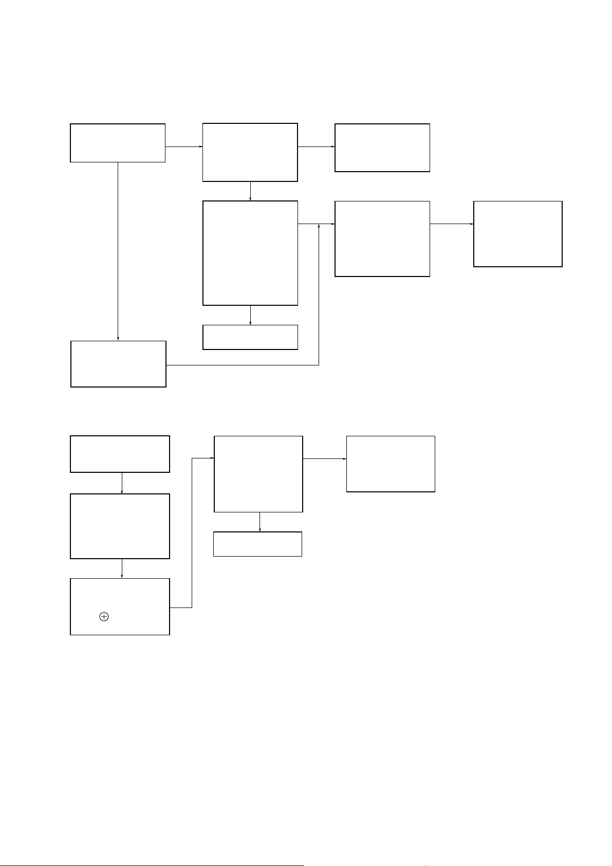
2. Pass-fail judgment of the optical device (KEM480AAA)
Perform pass-fail judgment to judge whether the repair of the optical device (KEM480AAA) is necessary.
2-1. Flow of drive section check
Ver. 1.5
Confirm whether
BD (BLX-104) can be
reproduced
YES
Confirm whether
DVD (HLX-513)/
CD (HLX-A1) can be
reproduced
Note: Refer to “2-11. OPTICAL PICK-UP BLOCK (KEM480AAA), WIRE (FLAT TYPE)” (page 20) about how to remove the COVER, DRIVE.
Confirm whether the
NO
NO
drive voltage is the
following values
Q205 pin 1 : 12 V
Q206 pin 1 : 5 V
YES
Confirm OP FFC cable
(Part No. 1-846-347-11)
and SPD FFC cable
(Part No. 1-846-349-61),
and replace it when it
has been damaged
Then, confirm whether
this unit operates
normally
YES
OK
Confirm F201, F202,
NO
F203 on the MB1002
board, and replace it
when it is open.
NO NO
Confirm whether the
optical device IOP
is normal in the
service mode
(Refer to “2-2. Flow
of optical device
IOP check”)
Replace the
optical device
(KEM480AAA)
(Refer to “3. Optical
device (KEM480AAA)
replacement”)
2-2. Flow of optical device IOP check
Turn the power on,
and change function
to “BD/DVD”
Press the buttons on
the remote commander
in order of [DISPLAY],
[0], [2], [1] [SUBTITLE],
and enter the service
mode
Press the buttons on
the remote commander
in order of [8], [7], [3],
[ ], and the
dIOP value is displayed
Confirm whether
value is the
specification value
Specification value:
BD : ±6 mA
DVD/CD: ±9 mA
YES
OK
NO
Replace the
optical device
(Refer to “3. Optical
device (KEM480AAA)
replacement”)
7
Page 8
HBD-E2100/E3100/E3200/E4100/E6100
Ver. 1.5
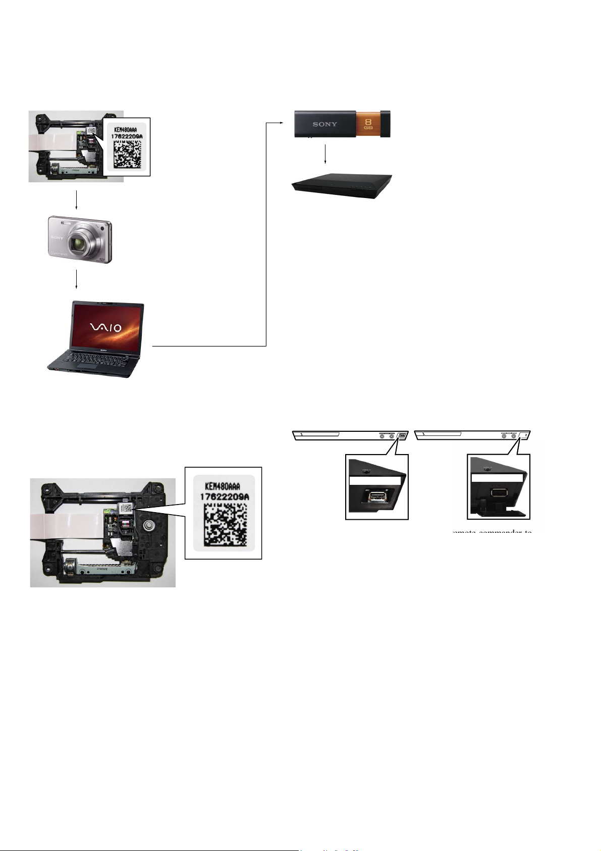
3. Optical device (KEM480AAA) replacement
Flow of replacement:
Note: The photo in fl ow is an image.
Barcode label on
new optical device
(KEM480AAA)
bottom side
Take photo (JPEG)
by digital camera
Change photo into
the text data with
the barcode decoder
Save the text data
to USB memory
(memory capacity
need not be 8GB)
Connect USB memory
with front USB connector
on this unit, and read the
text data by the service mode
Procedure:
1. Remove the INSULATOR (4 pieces) and broken optical device (KEM480AAA) from LOADING ASSY.
2. Take photo of the barcode on new optical device
(KEM480AAA) bottom side by digital camera.
3. Assemble the INSULATOR (4 pieces) to new optical device
(KEM480AAA), fi x (Torque value: 2 kgf) it to LOADING
ASSY with screw, and assemble this unit.
4. Drag & drop the taken photo by step 2 to “BDPRdec.exe”, and
make the text data (File name: BuData.txt).
5. Save the text data to USB memory.
6. Connect USB memory with front USB connector on this unit,
and turn the power on.
– Front view –
(E2100)
\/1
Front USB connector
(E3100/E4100/E6100)
\/1
Front USB connector
7. Press the [FUNCTION] button on the remote commander to
select “BD/DVD”.
8. Press the buttons on the remote commander in order of
[DISPLAY], [0], [2], [1], [SUBTITLE], and enter the service
mode.
9. Press the buttons on the remote commander in order of [8], [1],
[ENTER], and execute “[1] Drive OP data Write”. BDV must
select Mode 1.
10. Turn the power off after writing the OP data.
11. Turn the power on, and enter the service mode again.
12. Press the buttons on the remote commander in order of [8], [7],
[3], [ENTER], and the dIOP value is displayed.
13. Confi rm value is the following specifi cation value, and turn the
power off.
Specifi cation value:
BD : 6 mA
DVD/CD : 9 mA
14. Turn the power on, confi rm playback performance of the BD
(BLX-104)/DVD (HLX-514)/CD (HLX-A1).
15. Completely assemble this unit, and complete the repair.
8
Page 9
HBD-E2100/E3100/E3200/E4100/E6100
Ver. 1.5
NOTE OF REPLACING MB1002 BOARD OR WLAN/
BT COMBO CARD
When the MB1002 board or WLAN/BT COMBO card are replaced, please execute the below service mode.
1. Please update FW to M16.R.157
2. Whenever replace MB1002 board or WLAN/BT COMBO
CARD please execute “Reset to Factory Default Settings”
from XMB.
Procedure:
[Home menu
Setup Resetting Reset to Factory Default
Settings All Settings]
Next, go to service menu and execute “(1) Bluetooth Enable” and
“(3) Write Bluetooth device address to Registry”.
Finally check one touch NFC listening function at normal power
on.
Note: The operation in this mode must use a remote commander
and TV monitor.
1. Connect this unit with TV monitor.
2. Press the
Press button in order of the [DISPLAY] [0] [2] [1]
3.
(\/1) button to turn the power on.
[SUBTITLE] on the remote commander.
(Make the interval when each button is pressed within two
seconds)
4. Enter the BD service mode. The OSD menu on TV monitor can
be operated by remote commander.
5. Press [m] and Enter Diag.
6. Press [,] and Enter Bluetooth Device Test (Screen 1).
7. Enter (1) Bluetooth Enable, wait until the display show
“ Status : Bluetooth Enable Successful ” (Screen 2).
8. Enter (3) Write Bluetooth device address to Registry, wait until
the display show “Bluetooth Device Address” and “Status :
Write Successfull” (Screen 3).
9. Enter [RETURN] to the selection of test category.
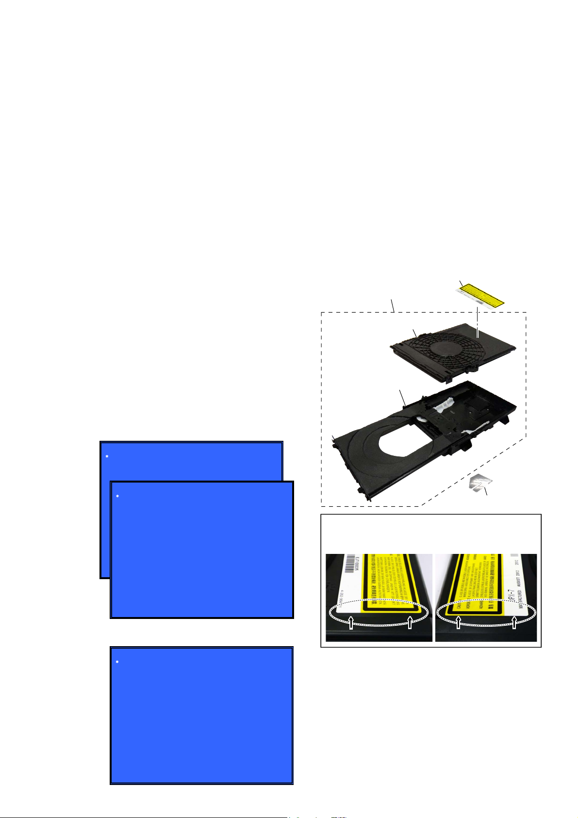
(Screen 1)
Diag
Category: Bluetooth Device Test
NOTE THE BD DRIVE (BPX-7) PARTS REPLACING
The mechanism blocks except optical device of BD drive (BPX-7)
are chiefl y composed of the following parts.
• HOLDER, CHUCK ASSY
• LOADING ASSY
• COVER, DRIVE
These parts are produced by two venders, it is not compatible.
Therefore, HOLDER, CHUCK ASSY and LOADING ASSY
are supplied by one pair as repair parts. Please exchange both
HOLDER, CHUCK ASSY and LOADING ASSY at the same
time.
COVER, DRIVE need not be exchanged at the same time.
Note 1: The laser caution label is not pasted to LOADING FOR SER-
VICE. Please peel off an original laser caution label, and paste
it to LOADING FOR SERVICE when you use LOADING FOR
SERVICE.
LABEL, LASER CAUTION
LOADING FOR SERVICE
HOLDER, CHUCK ASSY
LOADING ASSY
(Screen 2)
(Screen 3)
Diag
Category: Bluetooth Device Test
[1] Bluetooth Enable
[2] Bluetooth Disable
[3] Write Bluetooth device address to Registry
[4] Bluetooth Inquiry Test
Status : Bluetooth Enable Successful!
HELP: [UP][DOWN][ENT][RET]
Diag
Category: Bluetooth Device Test
[1] Bluetooth Enable
[2] Bluetooth Disable
[3] Write Bluetooth device address to Registry
[4] Bluetooth Inquiry Test
Bluetooth device address : 00:01:36:23:FD:CF
Status : Write Successful!
HELP: [UP][DOWN][ENT][RET]
COVER, DRIVE
/LPLWVDPSOHLQVWDWHRIODVHUFDXWLRQODEHO
If laser caution label is a condition of the figure below,
Note 2:
it is acceptable.
9
Page 10
HBD-E2100/E3100/E3200/E4100/E6100
–
Ver. 1.5
MODEL IDENTIFICATION
- Rear view -
Part No.
Model Part No.
E2100
E3100
E4100
E6100
E3200
4-438-896-0[]
4-438-896-1[]
4-438-896-2[]
4-438-896-3[]
4-438-896-6[]
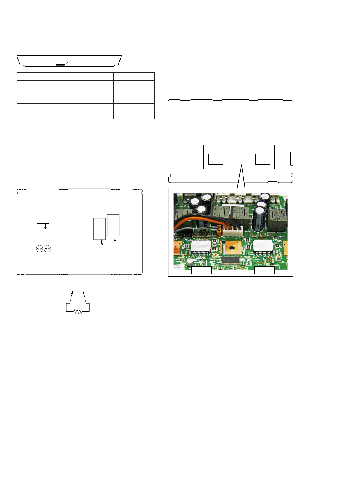
CAPACITOR ELECTRICAL DISCHARGE PROCESSING
When checking the board, the electrical discharge is necessary for
the electric shock prevention.
Connect the resistor to both ends of respective capacitors.
• Switching regulator
C207, C201, C402, C503, C504
SWITCHING REGULATOR (Conductor Side) –
NOTE OF REPLACING THE IC3102 AND IC3302 ON
THE AMP BOARD AND THE COMPLETE AMP BOARD
When IC3102 and IC3302 on the AMP board and the complete
AMP board are replaced, it is necessary to spread the compound
(GREASE (G-747)) 1KG) (Part No. 7-640-004-33 ) between parts
and heat sink.
Spread the compound referring to the fi gure below.
– AMP Board (Component Side) –
IC3102IC3302
C402
C504 C503
(To both ends of each capacitor)
800 :/2 W
C207
C201
IC3302 IC3102
10
Page 11

HBD-E2100/E3100/E3200/E4100/E6100
Ver. 1.5
CHECKING METHOD OF NETWORK OPERATION
It is necessary to check the network operation, when replacing the
MB1002 board. Check the operation of wireless and wired LAN,
according to the following method.
1. Checking Method of Wireless LAN Operation
Check that access point is recognized surely.
Necessary Equipment:
Wireless access point with router function (AP)
Procedure:
1. Press the [HOME] button on the remote commander to enter
the home menu.
2. Press the [m]/[M]/[<]/[,] buttons on the remote command-
er to select “Network Settings”“Internet Settings”, and press
] button on the remote commander.
the [
3. Press the [m]/[M] buttons on the remote commander to select
“Wireless Setup (built-in)”, and press the [ ] button on the
remote commander.
4. The system starts searching for access points, and displays a
list of up available network name (SSID).
5. Check that access point (SSID) is displayed on the searching
result.
Note: Refer to the instruction manual about details of the setting method.
2. Checking method of wired LAN operation
Check that access point is recognized surely.
Procedure:
1. Connect the main unit to the router or the hub, etc. with the
LAN cable.
2. Press the [HOME] button on the remote commander to enter
the home menu.
Press the [m]/[M]/[<]/[,] buttons on the remote commander
3.
to select “Network Settings”“Internet Settings”, and press
the [ ] button on the remote commander.
4. Press the [m]/[M] buttons on the remote commander to select
“Wired Setup”, and press the [ ] button on the remote commander.
5. Press the [m]/[M] buttons on the remote commander to select
“Auto”, and press the [ ] button on the remote commander.
6. Press the [,] button on the remote commander.
7. Press the [m]/[M] buttons on the remote commander to select
“Save & Connect”, and press the [ ] button on the remote
commander.
8. When “Internet Settings is now complete.” appears, then press
the [ ] button on the remote commander.
9. Press the [HOME] button on the remote commander to enter
the home menu.
10. Press the [m]/[M]/[<]/[,] buttons on the remote commander
to select “Network Settings”“Network Connection Diagnostics”,
and press the [ ] button on the remote commander.
11. Press the [<]/[,] buttons on the remote commander to select “IPV4” or “IPV6”, and press [ ] button on the remote
commander.
12. Press the [<]/[,] buttons on the remote commander to
select “Start”, and press the [ ] button on the remote commander.
13. Check that IP address can be acquired.
Note: Refer to the instruction manual about details of the setting method.
11
Page 12
HBD-E2100/E3100/E3200/E4100/E6100
Ver. 1.7
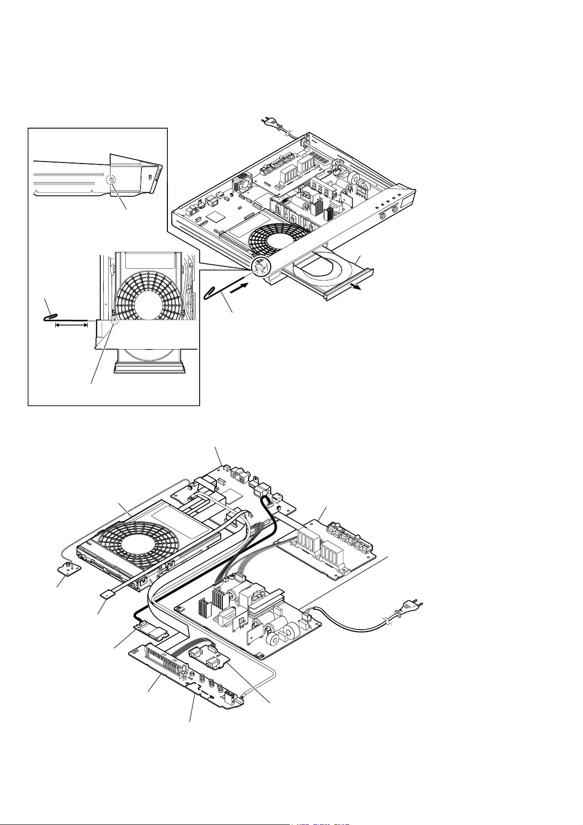
HOW TO OPEN THE TRAY WHEN POWER SWITCH TURN OFF
Note 1: After the case is removed, this work is done.
Note 2: Please prepare the thin wire (clip etc. processed to the length of 8 cm or more).
1 Remove the case.
(Illustration of disassembly is omitted.)
hole
– Side view –
Insert the clip etc.
processed to the
length of 8 cm or
more in the hole
on the side of the
chassis and push.
8 cm or more
Push after it inserts it in this hole well.
Note:
SERVICE POSITION
BD drive (BPX-7)
BD drive
tray
3
2 Insert the clip etc.
tray
– Top view –
MB1002 board
AMP board
POWER KEY board
RC-S801/A (WW)
card, WLAN/BT COMBO
12
PANEL board
NON-KARAOKE board
(EXCEPT SP, RU)
KARAOKE board
(SP, RU)
switching regulator (SWR1)
(3L392W-1) (US, CND, AEP, UK,
SAF, SP, TW, AUS,
TH, CH)
(3L392W) (E3, E51, PX, EA, E12,
E32, RU, MX6, AR)
• Abbreviation
AR
AUS : Australian model
CH : Chinese model
CND : Canadian model
E3 : 240 V AC area in E model
E12 : 220 – 240 V AC area in E model
E32 : 110 – 240 V AC area in E model
E51 : Chilean and Peruvian models
EA : Saudi Arabia model
MX6 : Latin-American model
PX : PX model
RU : Russian model
SAF : South African model
SP : Singapore model
TH : Thai model
TW : Taiwan model
: Argentina model
Page 13

DISASSEMBLY
• This set can be disassembled in the order shown below.
2-1. DISASSEMBLY FLOW
HBD-E2100/E3100/E3200/E4100/E6100
SECTION 2
Ver. 1.5
SET
2-3. CASE
(Page 15)
2-4. PANEL LOADING ASSY
(Page 15)
2-5. FRONT PANEL ASSY
(Page 16)
2-6. BD DRIVE (BPX-7)
(Page 16)
2-7. POWER KEY BOARD, WLAN/BT COMBO CARD,
KARAOKE BOARD (SP, RU), PANEL BOARD
(Page 17)
2-2. HOW TO BEND FFC
(Page 14)
2-8. MB1002 BOARD
(Page 18)
2-9. AMP BOARD
(Page 18)
2-10. SWITCHING REGULATOR (SWR1)
(Page 19)
2-11. OPTICAL PICK-UP BLOCK (KEM480AAA),
WIRE (FLAT TYPE)
(Page 20)
13
Page 14
HBD-E2100/E3100/E3200/E4100/E6100
Ver. 1.5
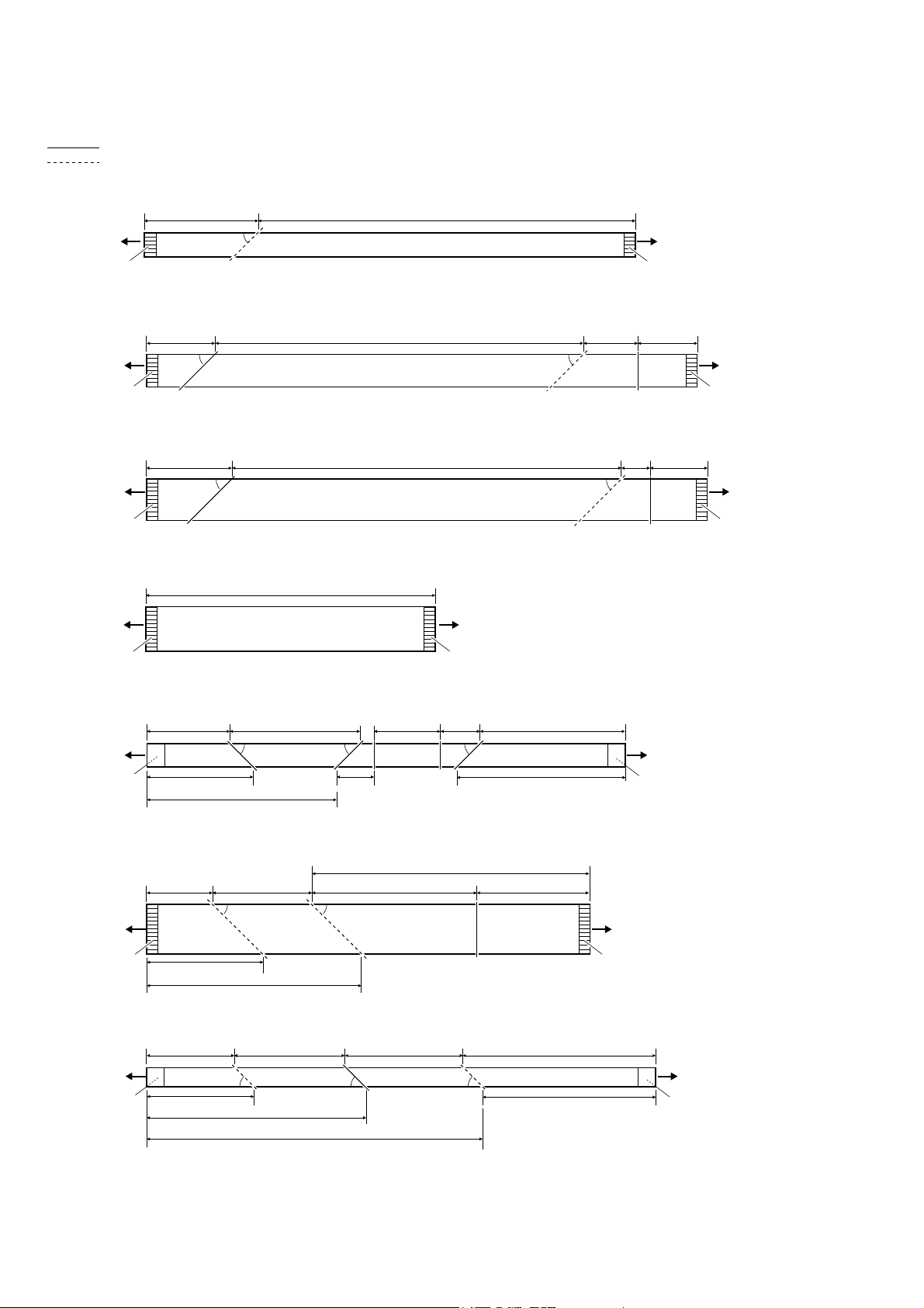
2-2. HOW TO BEND FFC
: Mountain fold
: Valley fold
wire (flat type) (8 core), length 260 mm (Ref. No. 52)
40 mm 220 mm
RC-S801/A
(WW)
The upper side
is contact side.
wire (flat type) (15 core), length 300 mm (Ref. No. 57) (EXCEPT SP, RU)
25 mm
MB1002 board
(CN805)
The upper side
is contact side.
wire (flat type) (21 core), length 305 mm (Ref. No. 57) (SP, RU)
MB1002 board
(CN803)
The upper side
is contact side.
45º
235 mm
45º 45º
30 mm
45º 45º
235 mm
MB1002
(CN806)
The upper side
is contact side.
18 mm 22 mm
20 mm
10 mm
PANEL board
(CN02)
The upper side
is contact side.
PANEL board
(CN01)
The upper side
is contact side.
wire (flat type) (24 core), length 105 mm (Ref. No. 105)
105 mm
MB1002 board
(CN707)
The upper side
is contact side.
wire (flat type) (9 core), length 252 mm (Ref. No. 206)
29 mm
MB1002 board
(CN660)
The lower side
is contact side.
flexible flat cable (45 core), length 231 mm (Ref. No. 207)
MB1002 board
(CN501)
The upper side
is contact side.
39 mm 12 mm
19 mm 49 mm 101 mm 62 mm
42 mm
78 mm 21 mm 12 mm 110 mm
45º 45º45º
97 mm
45º
91 mm
45º
AMP board
(CN3505)
The upper side
is contact side.
163 mm
120 mm
BD drive
(BPX-7)
The lower side
is contact side.
BD drive
(BPX-7)
The upper side
is contact side.
wire (flat type) (5 core), length 276 mm (Ref. No. 208)
33 mm 46 mm
MB1002 board
(CN670)
The lower side
is contact side.
45º 45º45º
39 mm
85 mm
143 mm
14
58 mm 139 mm
133 mm
BD drive
(BPX-7)
The lower side
is contact side.
Page 15
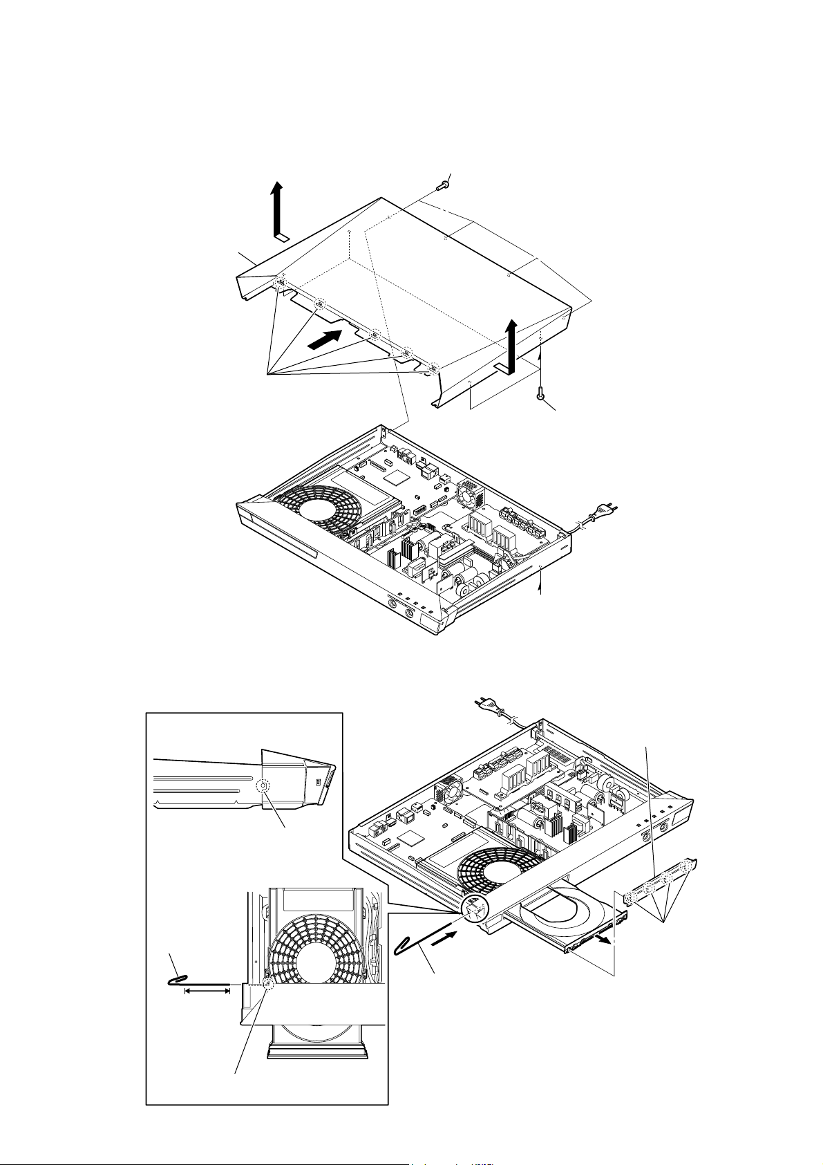
Note: Follow the disassembly procedure in the numerical order given.
2-3. CASE
6
7 case
HBD-E2100/E3100/E3200/E4100/E6100
Ver. 1.5
1 four screws (+BV3 (3-CR))
3 five claws
2-4. PANEL LOADING ASSY
4
5
A
2 four screws (+BV3 (3-CR))
A
hole
– Side view –
Insert the clip etc.
processed to the
length of 8 cm or
more in the hole
on the side of the
chassis and push.
8 cm or more
Push after it inserts it in this hole well.
Note:
4 panel loading assy
BD drive
3 four claws
2
1 Insert the clip etc.
tray
– Top view –
15
Page 16
HBD-E2100/E3100/E3200/E4100/E6100
Ver. 1.5
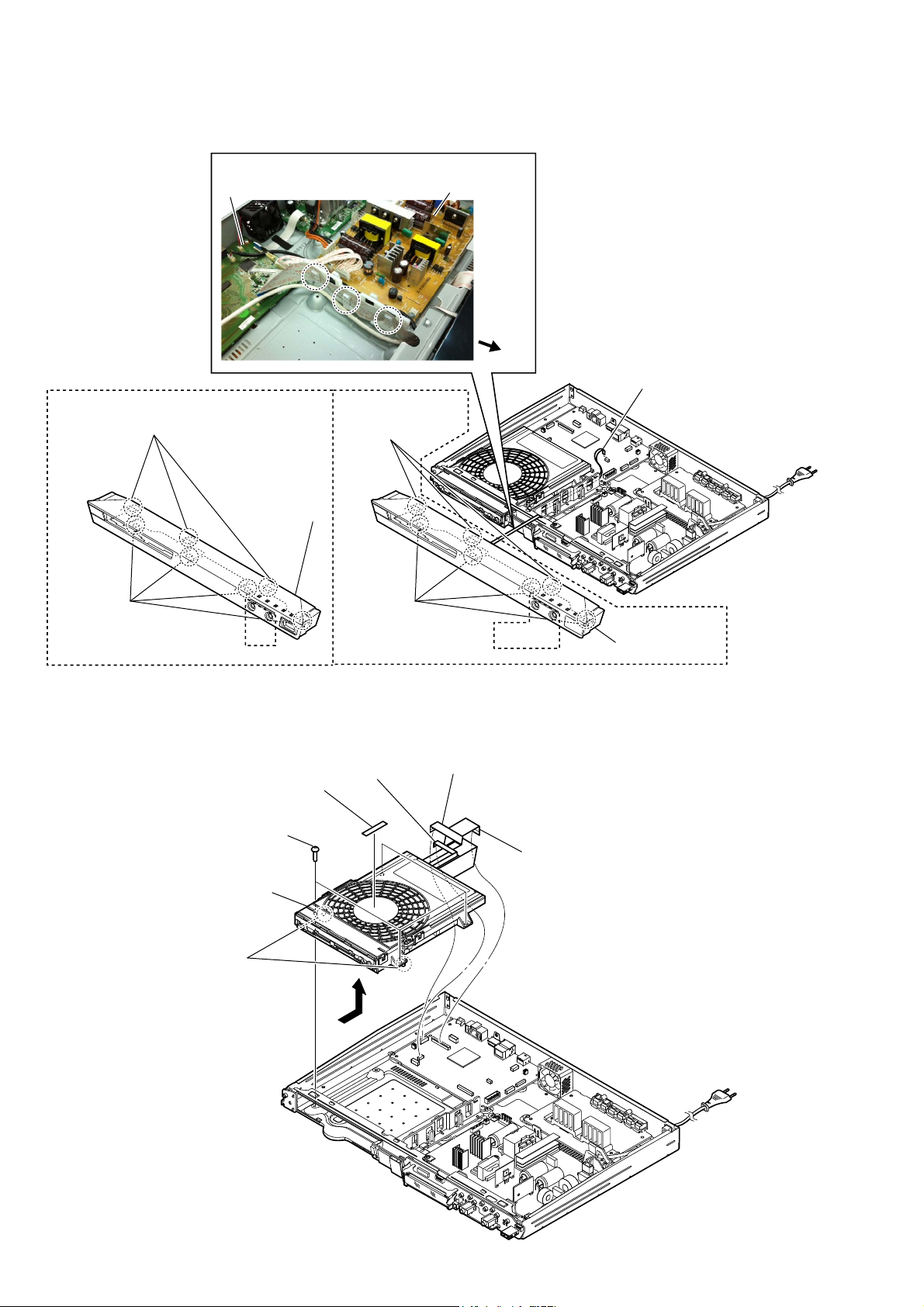
2-5. FRONT PANEL ASSY
3 three claws
2 four claws
:LUHVHWWLQJ
MB1002 board
4 front panel assy
switching regulator (SWR1)
(E3100/E4100/E6100)(E2100)
3 three claws
2 four claws
• Abbreviation
RU : Russian model
SP : Singapore model
front side
1 wire (flat type) (8 core)
(CN806)
2-6. BD DRIVE (BPX-7)
4 four screws
(+BV3 (3-CR))
8 BD drive BPX-7
5 boss
When you install the BD
Note:
drive (BPX-7), please match
the position of the boss two
places.
(SP)
3 wire (flat type)
(5 core) (CN670)
7 sheet, sound
6358
4 front panel assy
2 wire (flat type)
(9 core) (CN660)
1 flexible flat cable (45 core) (CN501)
6
16
Page 17
HBD-E2100/E3100/E3200/E4100/E6100
Ver. 1.5
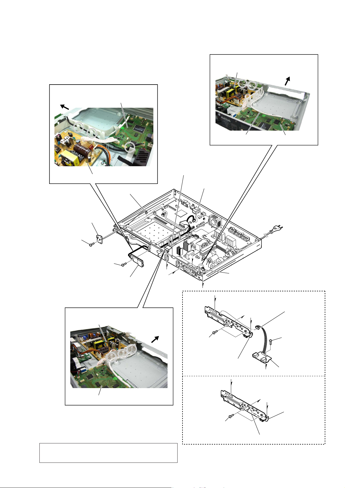
2-7. POWER KEY BOARD, WLAN/BT COMBO CARD, KARAOKE BOARD (SP, RU), PANEL BOARD
:LUHVHWWLQJ
switching regulator (SWR1)
front side
:LUHVHWWLQJ
front side
MB1002 board
switching regulator (SWR1)
3 POWER KEY board
2 one screw
(+BV3 (3-CR))
5 one screw
(+BV3 (3-CR))
6 card, WLAN/BT COMBO
:LUHVHWWLQJ
switching regulator (SWR1)
1 CN804 (2P)
front side
7 wire (flat type) (21 core) (CN01)
(SP, RU)
wire (flat type) (15 core) (CN02)
(EXCEPT SP, RU)
4 CN404 (5P)
G
D
F
E
(SP, RU)
D
0 two screws
(+BV3 (3-CR))
harness USB
9 harness (USB) CN51 (5P)
F
E
MB1002 board
8 CN03 (6P)
qs one screw
(+BV3 (3-CR))
MB1002 board
• Abbreviation
RU : Russian model
SP : Singapore model
Note: When replacing the WLAN/BT COMBO card, refer to
“CHECKING METHOD OF NETWORK OPERATION”
(page 11).
qa PANEL board
(EXCEPT SP, RU)
0 two screws
(+BV3 (3-CR))
D
G
F
qf NON-KARAOKE board
qd KARAOKE board
E
qa PANEL board
17
Page 18
HBD-E2100/E3100/E3200/E4100/E6100
Ver. 1.5
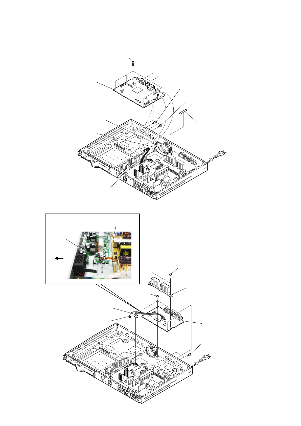
2-8. MB1002 BOARD
5 five screws
(+BV3 (3-CR))
8 MB1002 board
6 one screw
(+BV3 (3-CR))
7 one screw
(+B 3 u5)
3 wire (flat type)
(24 core) (CN707)
2-9. AMP BOARD
:LUHVHWWLQJ
AMP board
rear side
1 CN201 (2P)
2 tape
4 CN202 (8P)
switching regulator (SWR1)
1 CN101 (4P)
2 CN4 (2P)
3 four screws
(+BV3 (3-CR))
4 three screws
(+BV3 (3-CR))
5 heat sink (AMP 5.1CH)
7 AMP board
6 two screws
(+BV3 (3-CR))
18
Page 19
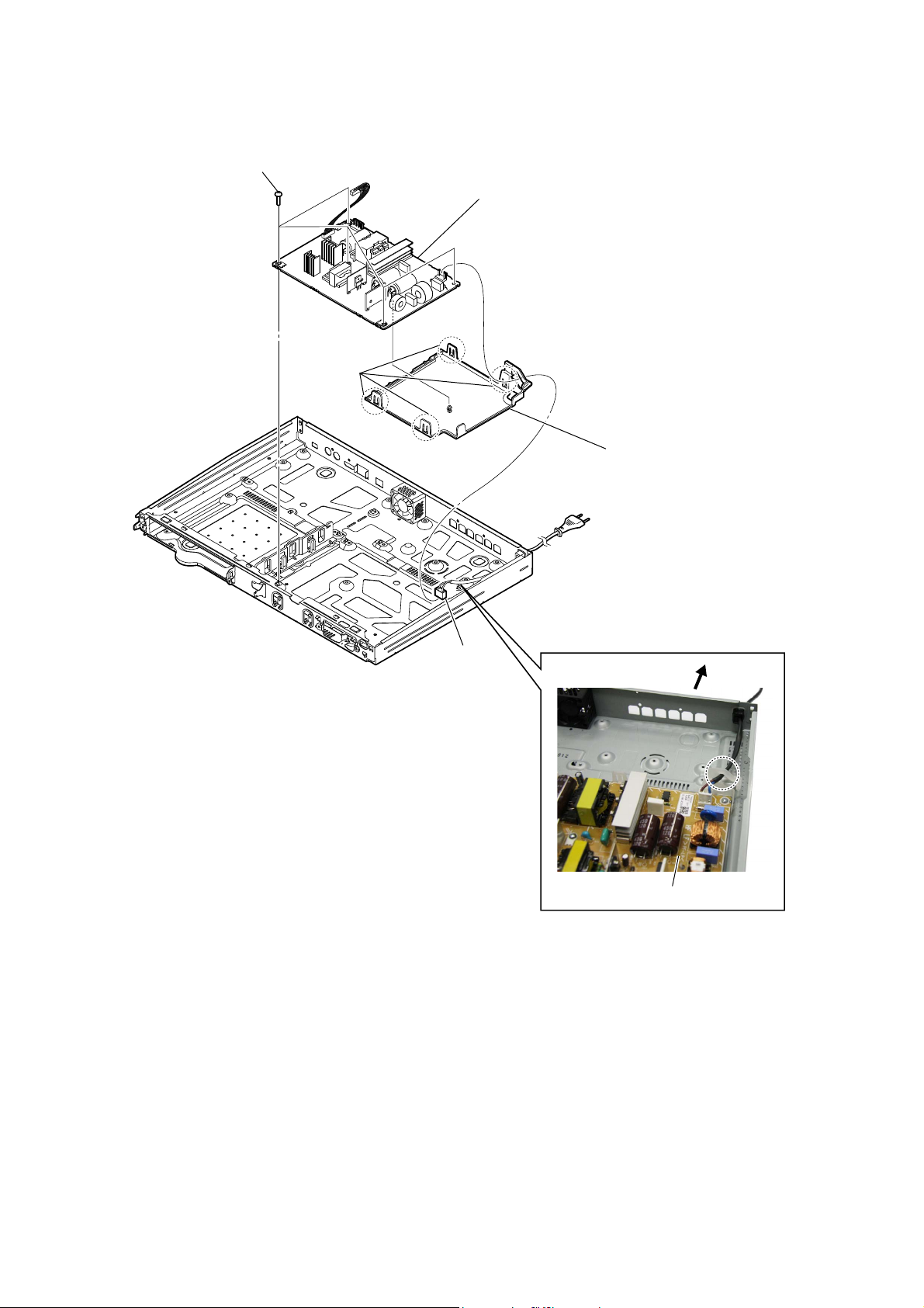
2-10. SWITCHING REGULATOR (SWR1)
2 five screws
(+BV3 (3-CR))
3 four claws
HBD-E2100/E3100/E3200/E4100/E6100
Ver. 1.7
5 switching regulator (SWR1)
(3L392W-1) (US, CND, AEP, UK, SAF, SP, TW, AUS, TH, CH)
(3L392W) (E3, E51, PX, EA, E12, E32, RU, MX6, AR)
4 insulation, bottom
1 CN1 (2P)
3RZHUFRUGVHWWLQJ
rear side
switching regulator (SWR1)
• Abbreviation
AR : Argentina model
AUS : Australian model
CH : Chinese model
CND : Canadian model
E3 : 240 V AC area in E model
E12 : 220 – 240 V AC area in E model
E32 : 110 – 240 V AC area in E model
E51 : Chilean and Peruvian models
EA : Saudi Arabia model
MX6 : Latin-American model
PX : PX model
RU : Russian model
SAF : South African model
SP : Singapore model
TH : Thai model
TW : Taiwan model
19
Page 20
HBD-E2100/E3100/E3200/E4100/E6100
Ver. 1.5
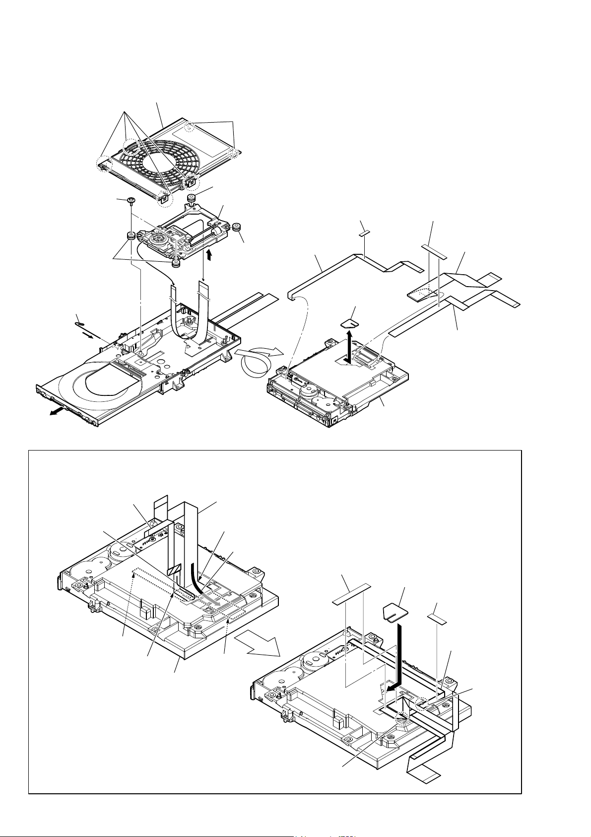
2-11. OPTICAL PICK-UP BLOCK (KEM480AAA), WIRE (FLAT TYPE)
1 four claws
6 two screws (S), float
0 insulator
4 Insert the thin
wire (clip etc.).
3 holder, chuck assy (T)
2 two claws
0 insulator
qa device, optical KEM480AAA
9
7
8
0 insulator
qs tape, non-halogene
qd wire (flat type)
(5 core)
qj
qf tape, FFC
qg flexible flat cable
(45 core)
qk cover, drive
qh wire (flat type)
(9 core)
5
– Bottom view –
,QVWDOODWLRQRIIOH[LEOHIODWFDEOHFRUHZLUHIODWW\SHFRUHDQGZLUHIODWW\SHFRUH
This illustration sees the loading assy (T) from bottom side.
Note:
3 wire (flat type) (9 core)
4 Through the hole
terminal face
Fold
loading assy (T)
1 flexible flat cable (45 core)
Fold
2 Through the hole
5 tape, FFC
terminal face
loading assy (T)
9 cover, drive
7 tape, non-halogene
8
6 wire (flat type)
(5 core)
Under the
guide
20
Under the guide
(Fold area)
Page 21
HBD-E2100/E3100/E3200/E4100/E6100
SECTION 3
TEST MODE
Ver. 1.5
COLD RESET
The cold reset clears certain data in this system without initialize
Personal Information and some BD operation data. Execute this
mode when returning the unit to the customers.
Procedure:
1. Press the [
] button to turn the power on.
?/1
2. Press the [x] and [VOL –] buttons simultaneously and hold
down (around 5 seconds).
3. The message “WAIT” appears then “RESET” appears on fl uo-
rescent indicator tube, then becomes standby states.
DEMO MODE
This mode let you lock the disc tray. When this mode is activated,
the disc will not eject when the [
] button is pressed. The message
Z
“D. LOCK” will be displayed on the fluorescent indicator tube.
Procedure:
1. Press the [
] button to turn the power on.
?/1
2. Press the [FUNCTION] button to select the “BD/DVD”.
3. Insert a disc.
4. During stop condition, press the [x] and [Z] buttons
simultaneously and hold down (around 5 seconds) until
“D. LOCK” displayed on the fluorescent indicator tube.
Releasing method:
Press the [x] and [Z] buttons simultaneously and hold down
(around 5 seconds) until “D. OFF” displayed on the fl uorescent
indicator tube.
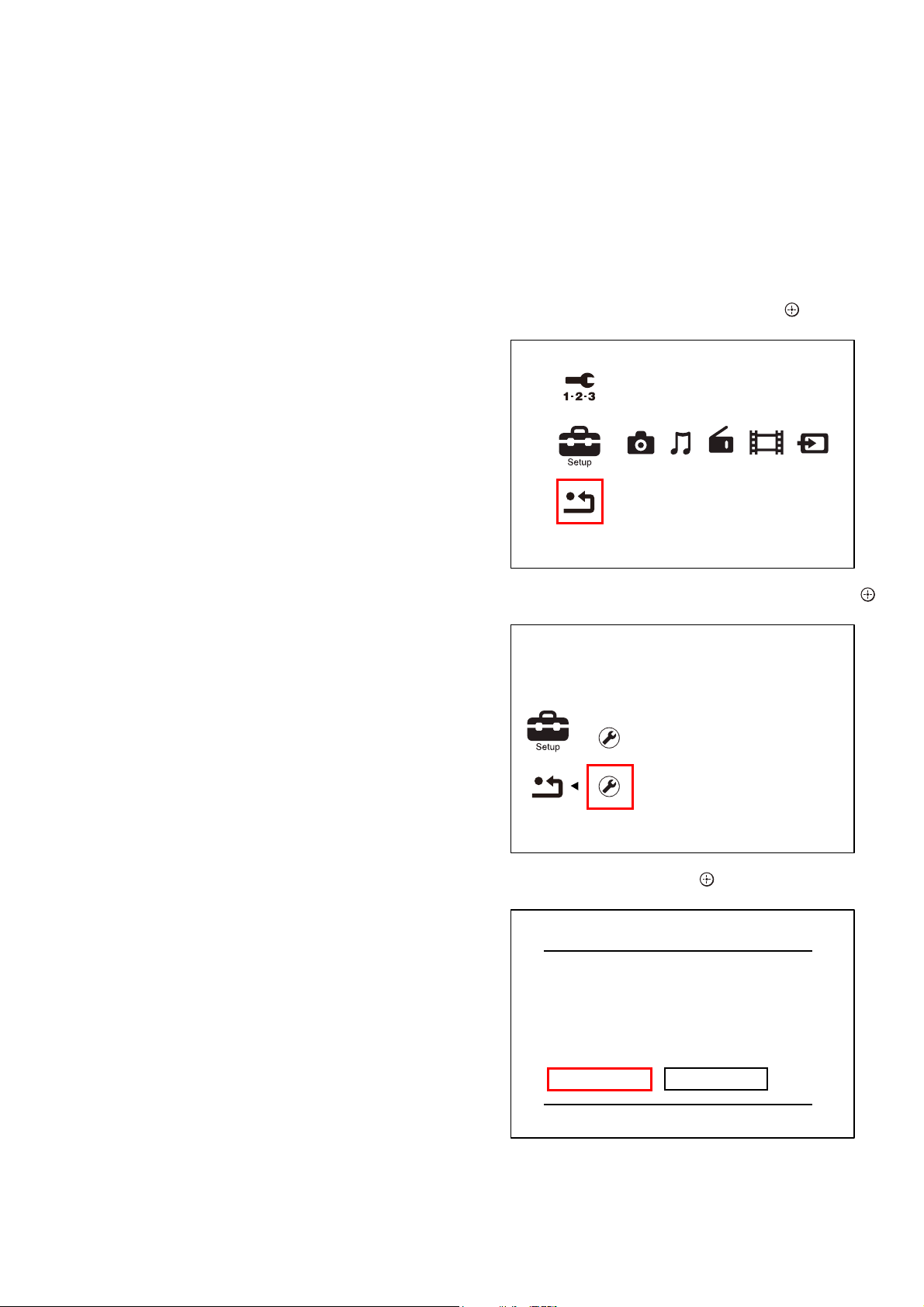
FACTORY INITIALIZE
Return all of the unit setting to their factory defaults.
Note 1: Disconnect the following connections when you use this mode.
USB
LAN
Note 2: The operation in this mode must use a remote commander and TV
monitor.
Procedure:
1. Press the [
] button to turn the power on.
?/1
2. Press the [HOME] button on the remote commander, and the
home menu is displayed.
3. Select “Setup” “Resetting”, and press the [
] button on the
remote commander.
Easy Network Settings
Resetting
PANEL TEST
Procedure:
1. Press the [
] button to turn the power on.
?/1
2. Press button in order of the [DISPLAY] [0] [0] [1]
[SUBTITLE] on the remote commander (Make the interval
when each button is pressed within two seconds).
3. All segments in fl uorescent indicator tube are lighted up. And
half segments in fl uorescent indicator tube are lighted up, oth-
ers half segments in fl uorescent indicator tube are lighted up,
then all segments in fl uorescent indicator tube are lighted up.
This operation is repeated.
4. In the state of step 3, press the [VOL +] button on the remote
commander and model information is displayed on the fl uores-
cent indicator tube.
Each time the [VOL +] button on the remote commander is
pressed, the display changes from destination information,
STR version, special mode in this order, and returns to the
model information display.
5. In the state of step 3, press the [FUNCTION] button on the
remote commander and “K 0” is displayed on the fluorescent
indicator tube.
“K 0” value increases whenever a button or sensor on the unit
is pressed. However, once a button or sensor has been pressed,
it is no longed taken into account.
All button and sensors on the unit are pressed, “OK” and “K 9”
are alternately displayed on the fluorescent indicator tube.
Releasing method:
To release from this mode, press the [
?/1
] button.
4. Select “Initialize Personal Information”, and press the [
button on the remote commander.
Reset to Factory Default Settings
Initialize Personal Information
Delete personal data when disposing
5. Select “OK”, and press the [ ] button on the remote commander.
Initialize Personal Information
The information below will be deleted.
Do you want to proceed?
- Playback history
- Internet video utilization information
OK
Cancel
]
21
Page 22
HBD-E2100/E3100/E3200/E4100/E6100
Ver. 1.5
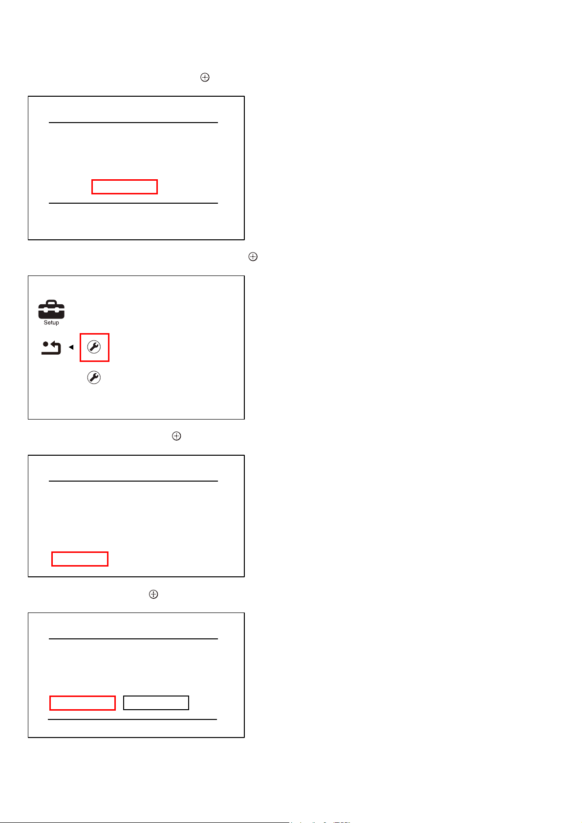
6. The message “Close” appears, and press the [
] button on the
remote commander.
Initialize Personal Information
Initialization complete.
Close
7. Select “Reset to Factory Default Settings”, and press the [
button on the remote commander.
Reset to Factory Default Settings
Restore each setting to the factory d
Initialize Personal Information
8. Select “All Settings”, and press the [ ] button on the remote
commander.
BD SERVICE MODE
Note: The operation in this mode must use a remote commander and TV
monitor.
Setting method of the BD service mode:
1. Connect this unit with TV monitor.
2. Press the [
] button to turn the power on.
?/1
3. Press button in order of the [DISPLAY] [0] [2] [1]
[SUBTITLE] on the remote commander. (Make the interval
when each button is pressed within two seconds)
4. Enter the BD service mode. The OSD menu on TV monitor
can be operated by remote commander.
1. Main Functions
• Diag
Performs unit test of devices installed on the board.
• Log
Error log is displayed. Displayed contents can also be saved in
]
an USB memory device.
• Factory Initialize
Restores the unit to its factory settings.
• Network
Checks the wired network connection.
• Version Up
• System Information
Displays the system information of the unit.
Displays information such as the software version, drive infor-
mation, etc.
• EMC Test Mode
Not used.
• Drive
Write drive OP data and check drive.
• HDD Mode
Not used.
Reset to Factory Default Settings
Screen Settings
Audio Settings
BD/DVD Viewing Settings
Parental Control Settings
System Settings
Network Settings
All Settings
9. Select “Start”, and press the [ ] button on the remote commander.
All Settings
Restore all settings to the factory default
settings. The system will turn off after
reset.
Start
Cancel
10. Initialization ends when the message “HELLO” on the
fl uorescent indicator tube disappears.
22
Page 23
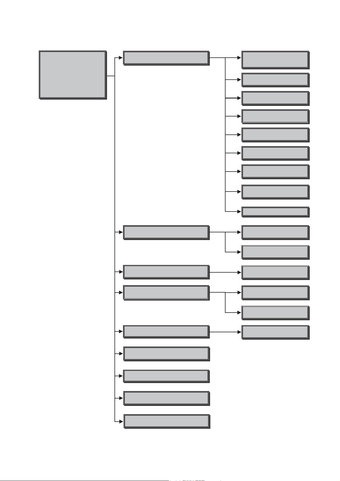
2. Menu Tree
HBD-E2100/E3100/E3200/E4100/E6100
Ver. 1.5
Service 0ode 0enu
Service 0ode 0enu
[1] DiaJ
[1] DiaJ
[2] LoJ
[2] LoJ
[3] Factory Initialize
[3] Factory Initialize
[4] Network
[4] Network
[5] Version Up
[5] Version Up
[6] System Information
[6] System Information
[7] (0&7HVW0RGH
[8] Drive
>@+''0RGH
DiaJ
'LDJ7HVW
Device Test
86%'$&,)FRQ0,&0),,3&
([WHUQDO+'0,7UDQVFRGHUWHVW
Video Test
Video output test
$udio Test
$udio output test
$udio Input Test
$XGLR,QSXW7HVW
:LUHOHVV/$17HVW
Only wireless model used
0LF7HVW
Not used
+'0,,QSXW7HVW
Not used
Transcorder Test
Not used
%OXHWRRWK'HYLFH7HVW
LoJ
Displays Error /RJ
Factory Initialize
,QLWLDOL]HGHIDXOWVHWWLQJ
Network
1Htwork diDJQRVLVIRUZLUHG
Version Up
DISC update
System Information
Displays system information
(0&7HVW0RGH
Not used
Error LoJ
Displays error loJ
+''/RJ
Not used
Start Initialize
,QLWLDOL]HGHIDXOWVHWWLQJIRUWKHXQLW
,IFRQILJ
View network status
3LQJ
&RQILUPQHWZRUNFRQQHFWLRQ
Start Update
6WDUWGLVFXSJUDGH
Drive
Write drive OP data and check drive
+''0RGH
Not used
23
Page 24
HBD-E2100/E3100/E3200/E4100/E6100
[
e
Ver. 1.5
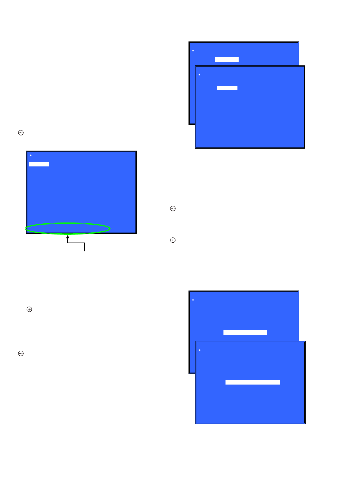
3. Service Mode Menu (Top Menu)
This is the top menu of service mode.
Each function is accessed from this screen.
Operation:
[1] Moves to Diag screen
[2] Moves to Log screen
[3] Moves to Factory Initialize screen
[4] Moves to Network screen
[5] Moves to Version Up (DISC version update) screen
[6] Moves to System Information screen
[7] Moves to EMC test mode screen (Not used)
[8] Moves to Drive screen
[9] Moves to HDD mode (Not used)
]/[m] Moves the cursor
[
M
[ ] Moves to the screen of the item selected with the cursor
(Screen 1)
Diag
Category:
Diag
Device Test
Category: Device Test
USB Host
Device:
Front USB Media check ... OK
Checking...
* Cursor is not displayed when the menu is fi rst displayed.
Service Mode Menu
[1] Diag
[1] Diag
[2] Log
[3] Factory Initialize
[4] Network
[5] Version Up
[6] System Information
[7] EMC Test Mode
[8] Drive
9] HDD mod
HELP : [UP] [DOWN] [ENT] [NUM]
HELP (currently available keys, etc.) is displayed
4. Diag (Device Test)
This screen is used to test devices mounted on the board.
Screen 1: Selects the test category
Operation:
[<]/[,] Selects the category
[m]/[ ] Moves to the selected category
[RETURN] Returns to the service top menu
(Screen 2)
HELP: [RIGHT] [UP] [ENT] [RET]
• Device Test: List of devices
USB Host : USB media check (front). Only one time.
5. Diag (Video/Audio Test)
This screen performs video and audio tests.
Screen 1: When video test category is selected
Operation:
[ ] Shows Color Bar
[
]/[RETURN] Returns to the selection of test category
M
Screen 2: When audio test category is selected
Operation:
] Generate TONE Sound
[
[
]/[RETURN] Returns to the selection of test category
M
• Video test:
Outputs a color bar (HDMI).
• Audio test:
TONE sound output (speaker & HDMI).
Diag
Category: Video Test
Screen 2: Device test
Selects the device to test after selecting Device Test in screen 1.
Operation:
[<]/[,] Selects the device to test
[ ] Executes the test
[M] Returns to selection of test category
[RETURN] Returns to selection of test category
• List of test categories
Device Test
Video Test
Audio Test
Audio Input Test
Wireless LAN Test
Mic Test (Not used)
HDMI Input Test (Not used)
Transcorder Test (Not used)
Bluetooth Device Test
24
(Screen 1)
(Screen 2)
[ENT] Show Color Bar
Diag
Category: Audio Test
HELP: [UP][ENT][RET]
[ENT] Generate TONE Sound
HELP: [UP] [ENT] [RET]
Page 25
HBD-E2100/E3100/E3200/E4100/E6100
Ver. 1.5
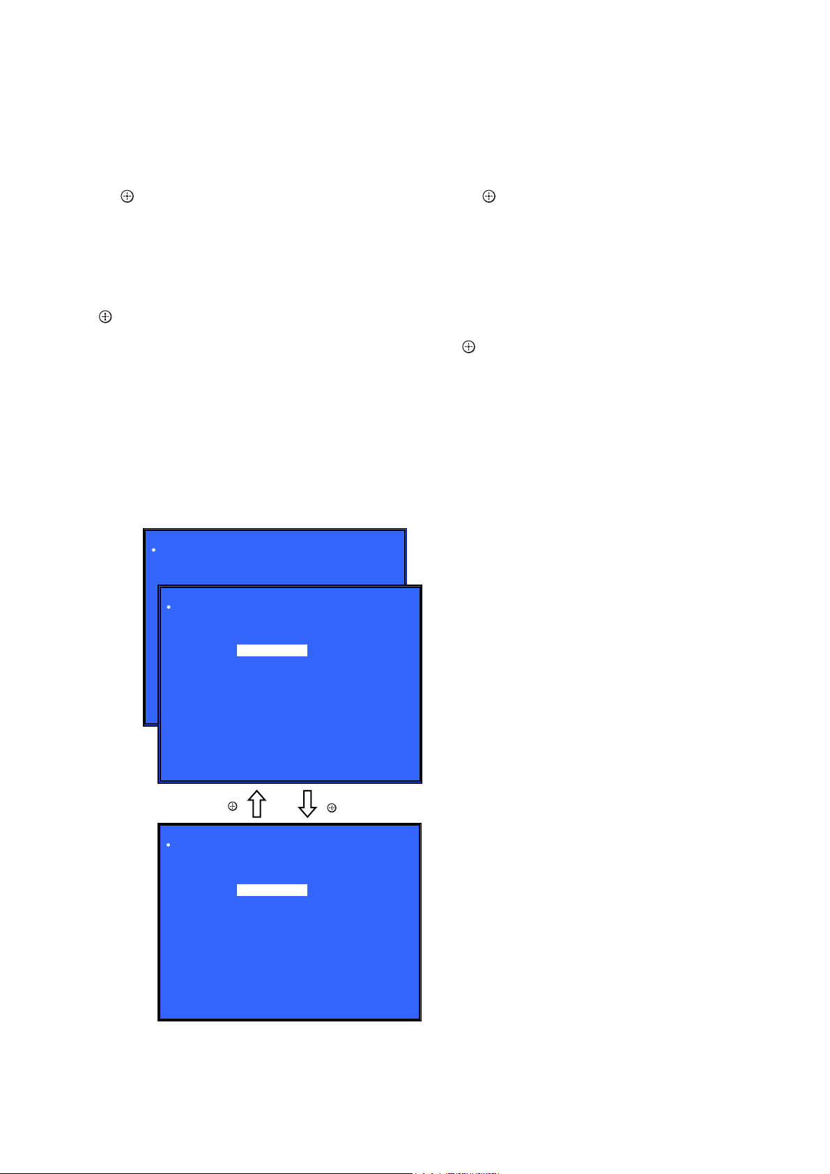
6. Diag (Audio Input Test)
This screen performs audio input test.
Screen 1: Select Audio Input Test Category
Operation:
[<]/[,] Selects the category
[m]/[ ] Activate the selected category
[RETURN] Returns to the service top menu
Screen 2: Select Input Device
After “Audio Input Test” selects in Screen 1, the device to test is
chosen.
Operation:
[M]/[m] Selects Device
[ ] Activate and Start Test/Stop
[RETURN] Returns to the selection of test category
• Device Test : Device List
Digital Input1 : CXD90019R-BA is inputted from Optical
Digital Input2 : CXD90019R-BA is inputted from ARC
Analog Input : CXD90019R-BA is inputted from AUDIO
• Audio Input Test
CXD90019R-BA is inputted from DIR/analog and outputs
LineOut (8ch) L and R.
Check tone sound by speaker connected with LineOut (8ch) L and
R.
(Input; LPCM 48kHz 2ch)
Diag
Category:
Diag
(Screen 1)
Audio Input Test
Category: Audio Input Test
Device:
[ENT] Start Input Sound
Digital Input 1
Digital Input 2
Analog Input
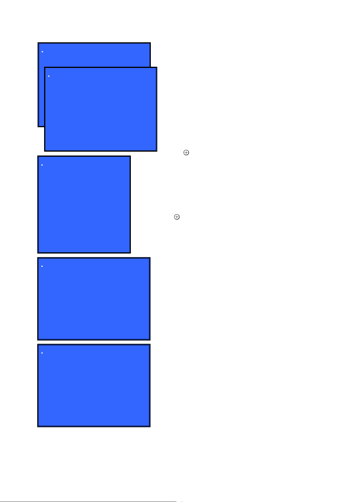
7. Diag (Wireless LAN Test)
This screen performs wireless LAN test.
Screen 1: Selects the Wireless LAN test category
Operation:
]/[,] Selects the category
[
<
[m]/[ ] Moves to the selected category
[RETURN] Returns to the service top menu
Screen 2: Wireless LAN test
[1] Show WLAN Hwinfo
[2] Connect to AccessPoint
[3] Start display RSSI value.
[4] Start Ping Test
Operation:
[M]/[m] Selects the test
[ ] Executes the test
[RETURN] Returns to selection of test category
Screen 2 : Select [1] Show WLAN HwInfo
• Viewing the display
Serial : Serial Number
Hard : Hardware Version
Mac : Mac Address
Screen 3 : Select [2] Connect to AccessPoint
Connect Access Point only with the following AP settings.
CERT: NO-ENCRYPT
WEPKEY: abcdef1234
PMK: ABCDE12345
SSID: SONY-Test-R
IPADDR: 192.168.1.100
NETMASK: 255.255.255.0
BROADCAST: 192.168.1.10
When connect to AP, Status is “Connected!”
When cannot connect to AP, Status is “can’t Connect!”
Screen 4 : Select [3] Start Display RSSI Value
Display RSSI value.
Screen 5 : Select [4 ] Start Ping Test
Ping Test.
IP address use the value of “192.168.1.10”.
(Screen 2)
HELP: [LEFT] [RIGHT] [UP] [DOWN] [ENT] [RET]
[ ]
Diag
Category: Audio Input Test
Device:
[ENT] Stop Input Sound
HELP: [LEFT] [RIGHT] [UP] [DOWN] [ENT] [RET]
Digital Input 1
Digital Input 2
Analog Input
[ ]
25
Page 26
HBD-E2100/E3100/E3200/E4100/E6100
Ver. 1.5
(Screen 1)
(Screen 2)
(Screen 3)
(Screen 4)
Diag
Category: Wireless LAN Test
Diag
Diag
Category: Wireless LAN Test
[1] Show WLAN HwInfo
[2] Connect to AccessPoint
[3] Start Display RSSI Value
[4] Start Ping Test
Serial : 200912313165535
Hard : 22
Mac : 00:01:36:23:FD:CF
HELP: [UP][DOWN][ENT][RET]
Diag
Category: Wireless LAN Test
[1] Show WLAN HwInfo
[2] Connect to AccessPoint
[3] Start Display RSSI Value
[4] Start Ping Test
CERT : NO-ENCRYPT
WEPKEY : abcdef1234
PMK : ABCDE12345
SSID : SONY-Test-R
IPADDR : 192.168.1.100
NETMASK: 255.255.255.0
BROADCAST : 192.168.1.10
Status : Connected!
HELP: [UP][DOWN][ENT][RET]
Diag
Category: Wireless LAN Test
[1] Show WLAN HwInfo
[2] Connect to AccessPoint
[3] Stop Display RSSI Value
[4] Start Ping Test
RSSI Value : 60
HELP: [UP][DOWN][ENT][RET]
8. Diag (MIC Input Test)
This screen performs MIC input test.
Note: Not used for the servicing.
9. Diag (HDMI Input Test)
This screen performs HDMI input test.
Note: Not used for the servicing.
10. Diag (Transcoder Test)
Note: Not used for the servicing.
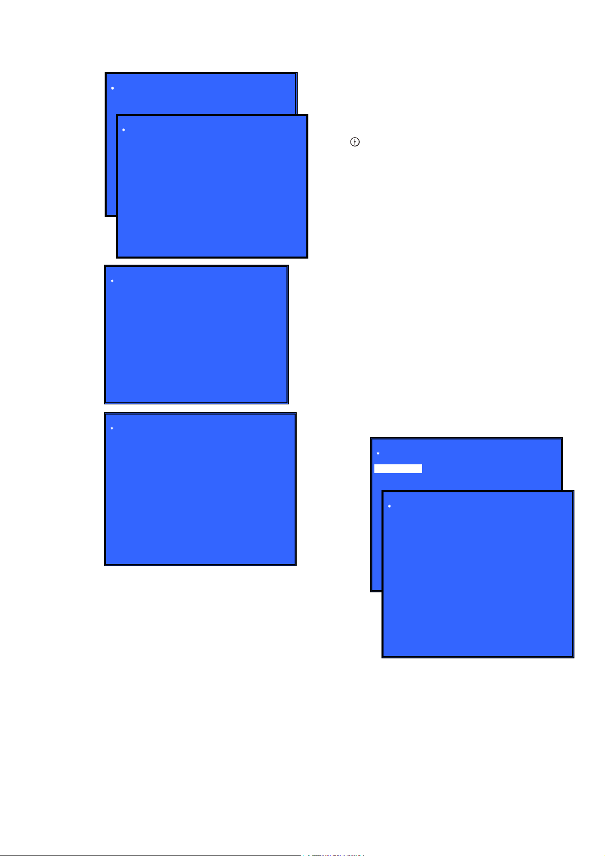
11. Diag (Bluetooth Device Test)
This screen performs Bluetooth Device Test.
Screen 1: Select Bluetooth Device Test Category
Operation:
[<]/[,] Selects the category
[m]/[ ] Activate the selected category
[RETURN] Returns to the service top menu
Screen 2: Select Bluetooth Device Test
Operation:
[1] Bluetooth Enable
[2] Bluetooth Disable
[3] Write Bluetooth device address to Registry.
[4] Bluetooth Inquiry Test
[M]/[m] Selects Device
[ ] Activate and Start Test
[RETURN] Returns to the selection of test category
Screen 2: Select [1] Bluetooth Enable
• Viewing the Status display, if
Successful: “Bluetooth Enable Successful!”
Fail: “Bluetooth Enable Fail!”
Screen 3 : Select [2] Bluetooth Disable
• Viewing the Status display, if
Successful: “Bluetooth Disable Successful!”
Fail: “Bluetooth Disable Fail!”
Screen 4 : Select [3] Store Bluetooth device address to
Registry
Display will show : Bluetooth device address : “xx:xx:xx:xx:xx:xx”
• Viewing the Status display, if
Successful: “Write Successful!”
Fail: “Write Fail!”
(Screen 5)
26
Diag
Category: Wireless LAN Test
[1] Show WLAN HwInfo
[2] Connect to AccessPoint
[3] Stop Display RSSI Value
[4] Start Ping Test
Ping To : 192.168.1.10
PING 192.168.1.10 OK!
HELP: [UP][DOWN][ENT][RET]
Page 27
HBD-E2100/E3100/E3200/E4100/E6100
Ver. 1.5
(Screen 1)
(Screen 2)
(Screen 3)
(Screen 4)
Diag
Category: Bluetooth Device Test
Diag
Category: Bluetooth Device Test
[1] Bluetooth Enable
[2] Bluetooth Disable
[3] Write Bluetooth device address to Registry
[4] Bluetooth Inquiry Test (not used)
Status : Bluetooth Enable Successful!
Status : Bluetooth Enable Fail!
HELP: [UP][DOWN][ENT][RET]
Diag
Category: Bluetooth Device Test
[1] Bluetooth Enable
[2] Bluetooth Disable
[3] Write Bluetooth device address to Registry
[4] Bluetooth Inquiry Test (not used)
Status : Bluetooth Disable Successful!
Status : Bluetooth Disable Fail!
HELP: [UP][DOWN][ENT][RET]
Diag
Category: Bluetooth Device Test
[1] Bluetooth Enable
[2] Bluetooth Disable
[3] Write Bluetooth device address to Registry
[4] Bluetooth Inquiry Test (not used)
Bluetooth device address : 00:01:36:23:FD:CF
Status : Write Successful!
Status : Write Fail!
HELP: [UP][DOWN][ENT][RET]
12. Log: Error Log (Output of each Log)
This screen displays the contents of each log.
Note: Do not refer to the displayed date.
Screen 1: Selects log
Operation:
[1]/[ ] Moves to the Error Log output screen
[RETURN] Returns to the top menu of the service mode
Screen 2: Displays the Error Log
Operation:
[<] Returns to the previous page
[,] Moves to the next page
[RETURN] Returns to the screen (Screen 1) that selects the log
type
[RED] Writes the log contents to an USB memory device
• Viewing the log display
Error Log:
[174] 2010/01/01 00:00:08 [ErrCode:0902A4053002]
[Index number] [Date] [Time] [Error code]
About copying log to USB memory device:
Press the [RED] button in each log display screen with the USB
memory device inserted into the unit.
Note: Please do not press the [RED] button immediately after USB mem-
ory is inserted.
Please do not pull out USB memory immediately after the [RED]
button was pressed.
Error Log:
When “getErrLogFile.trm fi le” exists in the USB memory de-
vice, errlog.log fi le is output.
Select Log
[1] Error Log
Error Log
02]
[174] 2010/01/01 00:00:08 [ErrCode:0902A4053002]
[175] 2010/01/01 00:00:08 [ErrCode:0902A4053002]
[176] 2010/01/01 00:00:08 [ErrCode:0902A4053002]
[177] 2010/01/01 00:00:08 [ErrCode:0902A4053002]
[178] 2010/01/01 00:00:08 [ErrCode:0902A4053002]
[179] 2010/01/01 00:00:08 [ErrCode:0902A4053002]
[180] 2010/01/01 00:00:08 [ErrCode:0902A4053002]
HELP : [DOWN][ENT][(NUM)]
(Screen 1)
(Screen 2)
[181] 2010/01/01 00:00:08 [ErrCode:0902A4053002]
[182] 2010/01/01 00:00:08 [ErrCode:0902A4053002]
[183] 2010/01/01 00:00:08 [ErrCode:0902A4053002]
[184] 2010/01/01 00:00:07 [ErrCode:0902A4053002]
[185] 2010/01/01 00:00:08 [ErrCode:0902A4053002]
[186] 2010/01/01 00:00:08 [ErrCode:0902A4053002]
<Page 1/20>
HELP : Press [RED] key to store log to Udisc.
27
Page 28
HBD-E2100/E3100/E3200/E4100/E6100
Ver. 1.5
13. Factory Initialize (Factory Settings)
There is a possibility that this mode cannot be correctly executed. Never use this mode.
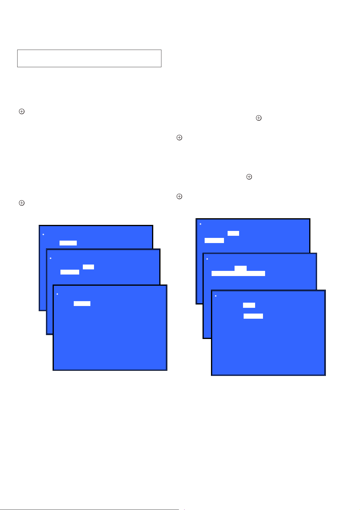
14. Network (Network Test Diagnosis Screen: Ifconfi g)
Network menu for the wired ethernet.
Screen 1: Ifconfi g Test
Operation:
[
] Activate Ifconfi g (Display network setting)
[,] Select ping test
[RETURN] Returns to the top menu of the service mode
Screen 2: Ping Test
Operation:
[<] Select Ifconfi g test
[RETURN] Returns to the top menu of the service mode
(The details of a Ping test are “14. Network (Network Test Diagnosis Screen: Ping)”)
Screen 3: Ifconfi g Test Active
Display Ifconfi g command results.
Operation:
[ ] Ifconfi g retry
[,] Select Ping Test
[RETURN] Returns to the top menu of the service mode
Network
Test: Ifconfig Ping
15. Network (Network Test Diagnosis Screen: Ping)
Ping test for the wired ethernet.
Screen 1: Ping Test
Operation:
[<] Select Ifconfi g test
[m] Ping execution preparation
[RETURN] Returns to the top menu of the service mode
Screen 2: The IP address of the Ping point is set up
(IP address input mode)
When “Ping to :>” is reversed, the [ ] button is pressed and IP
is inputted.
Operation:
[ ] Finish to input
[RETURN] Finish to input
[<] Finish to input and Select Ifconfi g Test
[0] to [9] Input Character sting ‘0-9’
Screen 3: Ping Test Active
When [START] is reversed, the [
] button is pressed and execute
ping.
Operation:
] Activate ping test
[
[M] The IP address of the ping point is set up
[RETURN] Returns to the top menu of the service mode
Network
Ifconfig
Test:
Ping To :
Ping
[START]
(Screen 1)
(Screen 2)
Network
Test: Ifconfig Ping
Ping To:
Network
HELP : [DOWN][ENT][(NUM)]
(Screen 3)
Test: Ifconfig Ping
IP 192. 168. 11. 2 MAC 00-16-01-85-21-A3
HELP : [DOWN][ENT][(NUM)]
HELP : [ENT]: Re/Exe [RIGHT]
[START]
(Screen 1)
(Screen 2)
(Screen 3)
Network
Test: Ifconfig
Ping to :> 192. 168. 200. 13
Test: Ifconfig
PING 192. 168. 200. 13 OK!
HELP: [ENT] : Start [UP] [LEFT]
Ping
[ENT] : Release
[RET] : Release
Network
Ping
Ping to : 192. 168. 200. 13
[START]
28
Page 29
HBD-E2100/E3100/E3200/E4100/E6100
Ver. 1.5
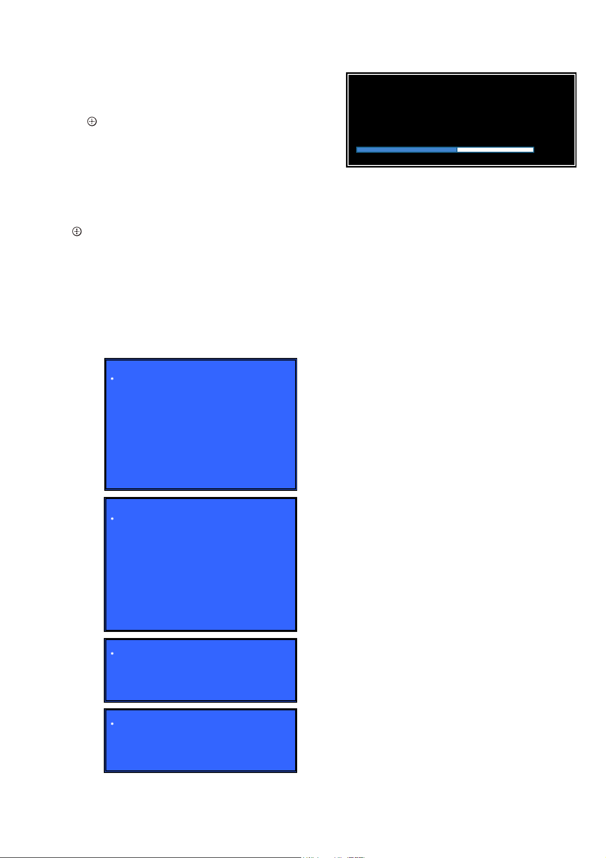
16. Version Up Test (Disc Update)
This screen performs version update test.
Operation:
]/[ ] Activate the selected category.
[
m
[RETURN] Return to Service Top Menu.
Screen 1: Select to Start Update
Operation:
[ENT] Start Update
[RETURN] Return to Top Menu
Screen 2: Insert Update Disc
Operation:
] Tray Close and Check start
[
[RETURN] Cancel
Screen 3/ Screen 4
Operation:
Mounting and checking the disc
If disc OK, upgrading will start
Screen 5
Operation:
Wait until the display bar show 100%.
(Screen 1)
Version Update
[ENT] Start Update
[RET] Return to Top Menu
HELP: [ENT][RET]
(Screen 2)
Version Update
Insert Update Disc
[ENT] Tray Close and Check start
[RET] Cancel
HELP: [ENT][RET]
(Screen 3)
Version Update
Now, mounting and checking…
(Screen 5)
Software Update
Software update has started.
Never turn off while performing update.
When the update is complete, the unit will automatically turn off.
17. System Information (System Information Display)
This screen displays system information.
Screen 1: Basic Information
Operation:
[,] Drive information (delta IOP of a drive is measured)
and wireless device information (not used) displayed
(go to Screen 2)
[RETURN] Returns to the top menu of the service mode
Screen 2: Drive and Wireless Information Menu
Operation:
[<] Basic Information displayed (go to Screen 1)
[RETURN] Returns to the top menu of the service mode
When delta IOP is measured, it becomes impossible to use the Version Up function.
Contents List:
Main LSIname
Model
Destination
Sequence Number
MAC
IP
IFCON IFCON Version
Bootloader Bootloader Version
Host Main Host Main Version
MicroBE MicroBE Version
Host Sub Host Sub Version
Middleware Middleware Version
ADSP ADSP Version
ADSP Coeff ADSP Coeff Version
IF Model
IF Dest
WLAN module Serial
WLAN module hw Version
WLAN module MAC Address
Drive Firm Revision
CD DIOP Delta IOP
DVD DIOP Delta IOP
BD DIOP Delta IOP
CD LD TIME LD Time
DVD LD TIME LD Time
Bluetooth Device Address
55%
(Screen 4)
Version Update
Upgrading, do not shut down the power!
29
Page 30
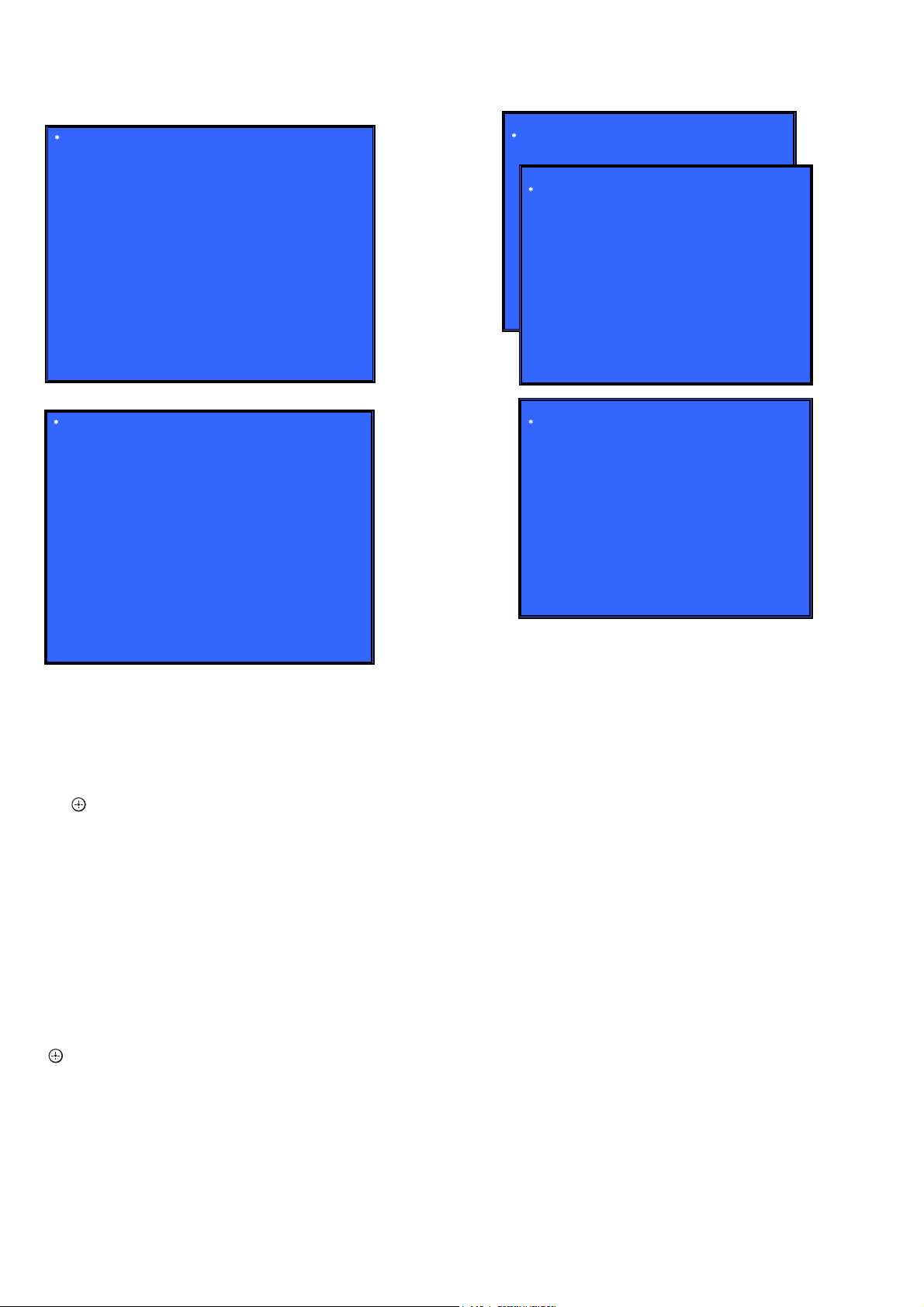
HBD-E2100/E3100/E3200/E4100/E6100
Ver. 1.5
(Screen 1)
System Information
Main LSIname:
Model:
Destination:
Sequence Number:
MAC:
IP:
IF-con Block0 Version:
Bootloader Version:
Host Main Version:
MicroBE Version:
Host Sub Version:
Middleware Version:
ADSP Version:
ADSP Coeff Version:
(Screen 1)
Drive
[1] Drive OP data Write
Drive OP data Write
Insert USB StorageDevice ...
Remove DISC and Close tray.
Disc : Load
Mode: 1
[ENT] Start
HELP : [RET] [RIGHT]
(Screen 2)
System Information
IF_MODEL:
IF_DEST:
WLAN module Serial:
WLAN module hw version:
WLAN module MAC Address:
Drive Firm Revision:
CD DIOP:
DVD DIOP:
BD DIOP:
CD LD TIME:
DVD LD TIME:
Bluetooth Device Address:
HELP : [RET] [LEFT]
18. Drive
This menu is used to operate the drive using drive-related diagnostic and tools.
Screen 1: Selecting items under *Drive
Operation:
[
]/[m] Selects the category
M
[m]/[ ] Activate the selected category
[RETURN] Returns to the top menu of the service mode
[1] Drive OP data Write
[2] Servo Parameter Check Menu
[3] Servo Signal Check Menu
[4] S-Curve Check Menu
[5] Readability Check Menu
[6] OP Position Check Menu
[7] OP Check Menu
[8] Load Eject Aging
[9] Spindle Control Check Menu
[10] FA Test Mode
(Screen 2)
(Screen 3)
HELP: [ENT] [RET]
Drive OP data Write
Insert USB StorageDevice ...
Remove DISC and Close tray.
[ENT] Start
NG - USB is not find
OK - OP data write
HELP: [ENT] [RET]
Screen 2: To start OP data Write
Operation:
] Starts
[
Screen 3: Show OP data Write result
Operation:
NG - USB is not fi nd
OK - OP data write
• Drive Test
For drive operating check. Service is only use Drive OP data write
to rewrite OP data after change of new CPU.
30
Page 31
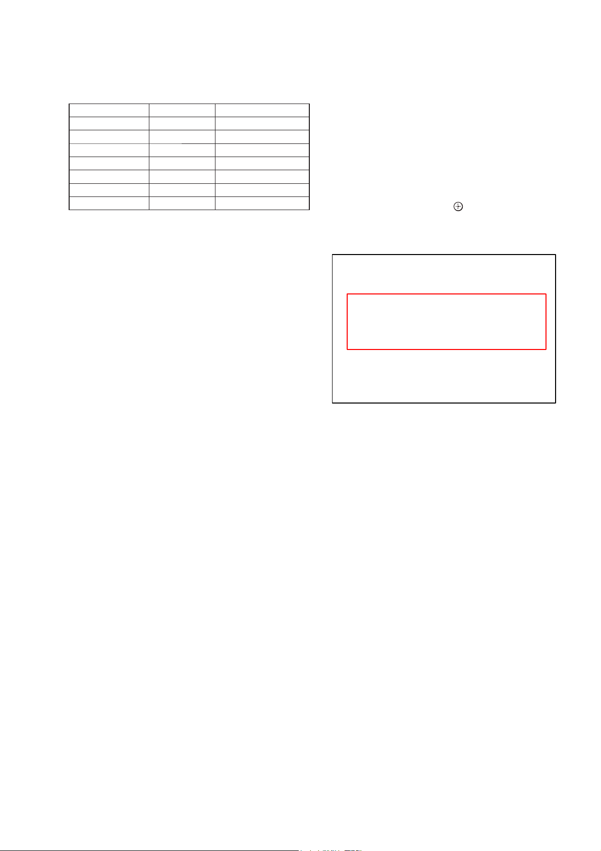
HBD-E2100/E3100/E3200/E4100/E6100
Ver. 1.5
CONFIRMATION ITEM
1. Playback Operation Confi rmation
1-1. Test Disc
Part No. Description Layer
J-6090-199-A BLX-104 Single Layer
J-6090-200-A BLX-204 Dual Layer
J-2501-307-A CD (HLX-A1)
J-2501-305-A HLX-513 Single Layer (NTSC)
J-2501-306-A HLX-514 Dual Layer (NTSC)
J-6090-077-A HLX-506 Single Layer (PAL)
J-6090-078-A HLX-507 Dual Layer (PAL)
Note: Refer to the service manual of BDP-BX1/S350 (Part No. 9-883-
989-1[]) (page 1-3 to 1-14E) for the use of BLX-104/204.
Operation and Display:
1. BLX-104
Procedure:
1. Select 23.976Hz/1080p.
2. Play “4.Motion picture”.
3. Check whether player can play back or not.
4. Check each outputs.
Video:
Composite/S Video/component/HDMI.
Audio:
Speaker out.
* When 1080/24p monitor is nothing, 1080i (59.94Hz or 50Hz)
can use instead of 1080/24p.
However this is temporary correspondence.
* When the output of HDMI is 1080p, the signal of Composite/S
Video/Component are not output.
It is necessary to lower the output of HDMI to 1080i or less.
2. Networking Confi rmation
Confi rm it according to the following procedure when you confi rm
the connection of the network.
Note: Do not execute “Network Connection Diagnostics” of “Network
Settings” of the home menu with only the router connected.
Procedure:
1. Connect the router with the unit with LAN cable.
2. Turn on the power of the unit and the router.
3. Press the [HOME] button on the remote commander, and the
home menu is displayed.
4. Select “Setup” “Network Settings” “Network Connec-
tion Status”, and press the [
] button on the remote com-
mander.
5. Confi rm IP address are displayed in “IP Address”, “Subnet
Mask” and “Default Gateway”.
Physical Connection: XXXX
Internet Access: XXXX
IP Address Setting: XXXX
IP Address: XXX.XXX.XXX.XXX
Subnet Mask: XXX.XXX.XXX.XXX
Default Gateway: XXX.XXX.XXX.XXX
DNS Settings: XXXX
Primary DNS: XXX.XXX.XXX.XXX
Secondary DNS: XXX.XXX.XXX.XXX
MAC Address: XXX.XXX.XXX.XXX
2. BLX-204
Procedure:
1. Select 1080i (59.94Hz or 50Hz).
2. Play “4.Motion picture”.
3. Check whether player can play back or not.
(Check the picture and sound output)
3. CD (HLX-A1)
Procedure:
Check whether player can play back or not.
(Check the sound output)
4. HLX-513/514 (NTSC), HLX-506/507 (PAL)
Procedure:
1. After displayed Main Menu, select “1.Video Signal”.
2. Play “1.Color bar 100%”.
(Check the picture and sound output)
3. Return to Menu.
4. Play “Demonstration 4:3” or “Demonstration 16:9”.
(Check the picture and sound output)
1-2. Playback operation confi rmation
Confi rm operation in each signal/output mode of test disc (BLX-
104/204) according to the content of the repair.
Note: “AV Sync.” doesn’t operate.
31
Page 32
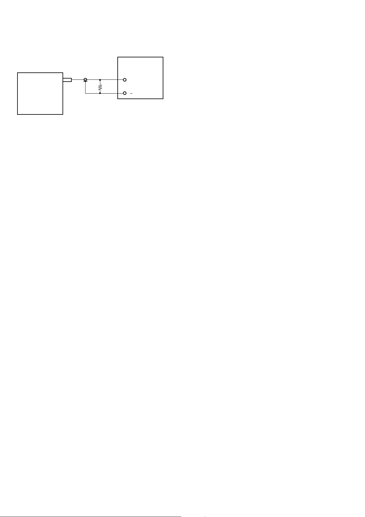
HBD-E2100/E3100/E3200/E4100/E6100
Ver. 1.5
SECTION 4
ELECTRICAL CHECK
FM AUTO STOP CHECK
generator
SET
+
75 :
Procedure:
1. Turn the power on.
2. Input the following signal from Signal Generator to FM antenna input directly.
Carrier frequency : A = 87.5 MHz, B = 98 MHz, C = 108 MHz
Deviation : 75 kHz
Modulation : 1 kHz
ANT input : 35 dBu (EMF)
Note: Please use 75 ohm “coaxial cable” to connect SG and the set. You
cannot use video cable for checking.
Please use SG whose output impedance is 75 ohm.
3. Set to FM tuner function and scan the input FM signal with
automatic scanning.
4. Confi rm that input Frequency of A, B and C detected and auto-
matic scanning stops.
The stop of automatic scanning means “The station signal is received in good condition”.
32
Page 33
HBD-E2100/E3100/E3200/E4100/E6100
SECTION 5
TROUBLESHOOTING
Ver. 1.5
Check that harness is inserted normally at CN301 and
CN202. When harness is inserted normally, exchange the
switching regulator (SWR1).
No
Check that the output voltages of the switching regulator
(SWR1) are the following value.
CN301 pin 1: 12 V (FEUNSW12V)
CN301 pin 2: 12 V (ICUNSW12V)
CN301 pin 3: 12 V (UNSW12V)
No
Exchange the damaged fuse or thermistor. Exchange the
complete MB1002 board, when the power is not turned on,
even if you exchange fuses.
No
Yes
Yes
Check that the following fuses and thermistor are not damaged.
TH802/F802/F201/F202/F203
Exchange the complete MB1002 board.
No
Check the following power control signal in the power on state.
(Normally voltage: +3.3 V)
MB1002 board IC801 pin 36 to 38
(PCONT1 to PCONT3)
Power supply IC is damaged. Exchange the power supply IC.
No
Check each voltage with reference to the schematic diagrams,
and check that there is no problem in them.
Yes
Check the related IC on the MB1002 board.
Yes
Pin 25 (PCONT_FL)
Insert normally the harness and power ON again.
No
Check that harness is inserted normally at CN101
Yes
Switching supply board damage. Exchange the complete
switching supply board.
No
Yes
Remove harness of CN101, CN4, FFC CN3505.
Yes
Measure switching supply board CN101 pin4 <-> pin1,
(normal voltage > 30V)
AMP board damage.
Exchange the complete AMP board.
Yes
The power is turned on.
Power Check Flow (1/2)
No
Protect mode happened “PROTECT”
display appears on fluorescent tube.
A
33
Page 34
HBD-E2100/E3100/E3200/E4100/E6100
Ver. 1.5
Refer to the “HDMI Check Flow” on page 35.
No
Check that a picture is outputted normally.
No
No
Perform and check [Audio Settings] -
[Speaker Settings] - [Test Tone] in the menu
screen, or reinsert the speaker cables.
Change FFC.
Insert to AMP CN3505
No
Check that each speaker is connected normally.
Refer to the “2-1. Flow of drive section check” on page
Optimize the speaker settings.
7 on original service manual.
No
Refer to the “Power Check Flow (1/2)” on page 33.
No
Front/Center/Surround/Subwoofer
No
No
Yes
Check that the signal is input to AMP board IC3001.
Pin 22, 23, 24, 25, 27
Yes
Exchange the IC3001.
Part No. 6-718-103-01
Description IC TAS5538DGGR
No
Check that the PWM signal is outputted from the
following pins.
AMP board IC3001 pin 39, 40, 48, 49, 42, 43, 54, 55
Exchange the IC3102.
Part No. 6-719-138-01
Description IC STA516BF13TR-A
No
Yes
Check that the signal is outputted from the following
pins.
AMP board IC3102
pin 10, 11 (SP FRONT R)
pin 16, 17 (SP FRONT L)
Yes
Pin 2, 3, 8, 9 (SP SUBWOOFER)
Exchange the IC3302.
Part No. 6-719-138-01
Description IC STA516BF13TR-A
No
Check that the signal is outputted from the following
pins.
AMP board IC3302
pin 10, 11, 16, 17 (SP CENTER)
pin 2, 3 (SP SUR R)
Pin 8, 9 (SP SUR L)
A
Power Check Flow (2/2)
Yes
Check that a sound is outputted normally.
34
Yes
Check that [Audio Settings]-[Audio output] in the menu
screen is “Speaker”.
Check that the drive is operating normally.
Yes
Check that each power supply is supplied to the audio
block.
Yes
Check that a sound is normally outputted from each
speaker.
Page 35
HBD-E2100/E3100/E3200/E4100/E6100
Ver. 1.5
Refer to the “2-1. Flow of drive section check” on page 7
No
on original service manual.
Refer to the “Power Check Flow (1/2)” on page 33.
No
No
Check the settings on the menu screen.
No
Refer to the “Power Check Flow (1/2)” on page 33.
Refer to the “Power Check Flow (1/2)” on page 33 to
No
Check that the input voltage of the following pin is 3.3V.
No
check on power control signal for PCONT_3
MB1002 board IC408 pin 1 (CONT)
Yes
Exchange the IC408.
Part No. 6-718-999-01
Description IC MM1839A50NRE
No
Check that the input voltage of the following pin is 3.3V.
No
Yes
Exchange the Q204.
MB1002 board Q204 pin 4 (CONT)
Part No. 6-553-007-01
Description TR PMG85XP
Exchange the CN401
Note: When CN401 is exchanged, be careful of the
quality of soldering enough.
Part No. 1-821-398-41
No
Description HDMI CONNECTOR (HDMI OUT ARC)
Yes
HDMI Check Flow
Check that the drive is operating normally.
Check that each power supply is supplied.
Yes
Check that only the digital output (HDMI) is affected.
Yes
Yes
Check that the input voltage of the following pin is 5.5 V.
MB1002 board IC408 pin 5 (VIN)
Check that the output voltage of the following pin is 5 V.
Yes
MB1002 board IC408 pin 4 (VOUT)
Check that the output voltage of the following pin is 3.3V.
Yes
MB1002 board Q204 pin 6
Check that there are no abnormalities in CN401.
Yes
Perform other analyses.
35
Page 36
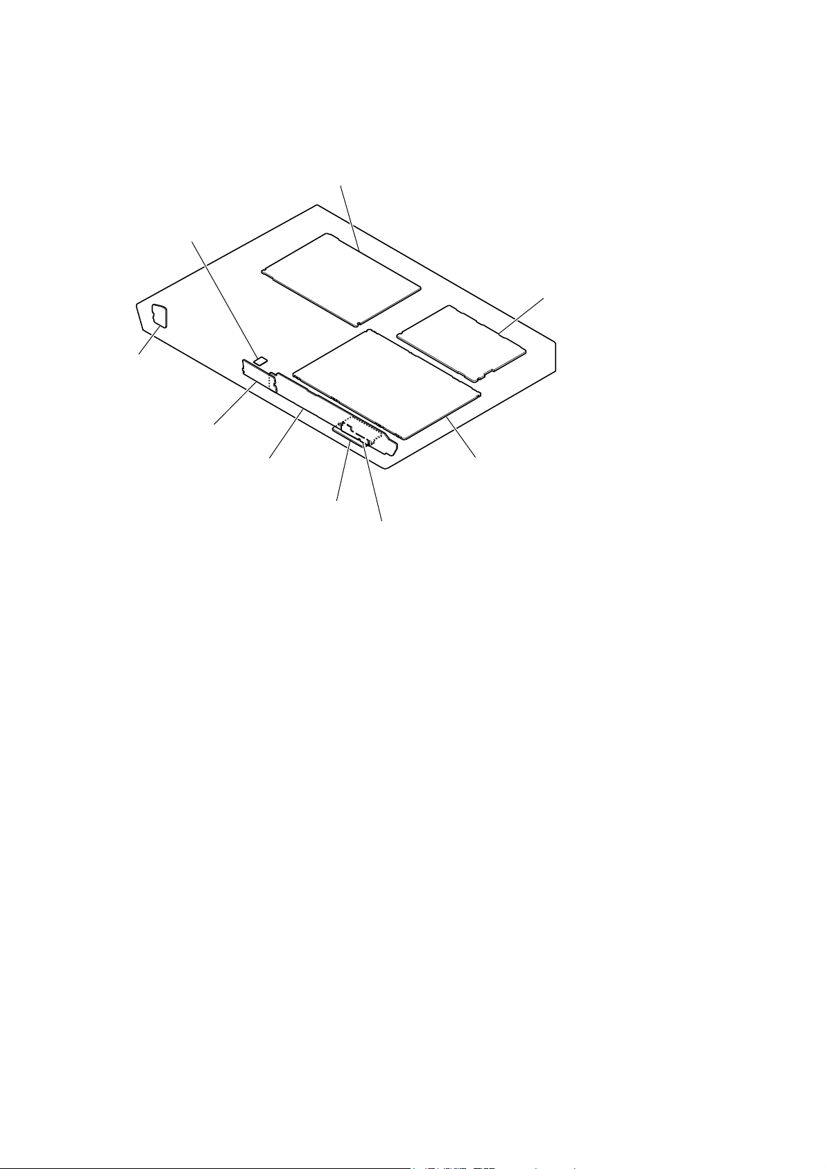
HBD-E2100/E3100/E3200/E4100/E6100
Ver. 1.7
SECTION 6
DIAGRAMS
• Circuit Boards Location
MB1002 board
RC-S801/A (WW)
POWER KEY board
card, WLAN/BT COMBO
AMP board
PANEL board
KARAOKE board (SP, RU)
NON-KARAOKE board (EXCEPT SP, RU)
switching regulator (SWR1)
(3L392W-1) (US, CND, AEP, UK, SAF, SP, TW, AUS,
TH, CH)
(3L392W) (E3, E51, PX, EA, E12, E32, RU, MX6, AR)
• Abbreviation
AR : Argentina model
AUS : Australian model
CH : Chinese model
CND : Canadian model
E3 : 240 V AC area in E model
E12 : 220 – 240 V AC area in E model
E32 : 110 – 240 V AC area in E model
E51 : Chilean and Peruvian models
EA : Saudi Arabia model
MX6 : Latin-American model
PX : PX model
RU : Russian model
SAF : South African model
SP : Singapore model
TH : Thai model
TW : Taiwan model
36
Page 37
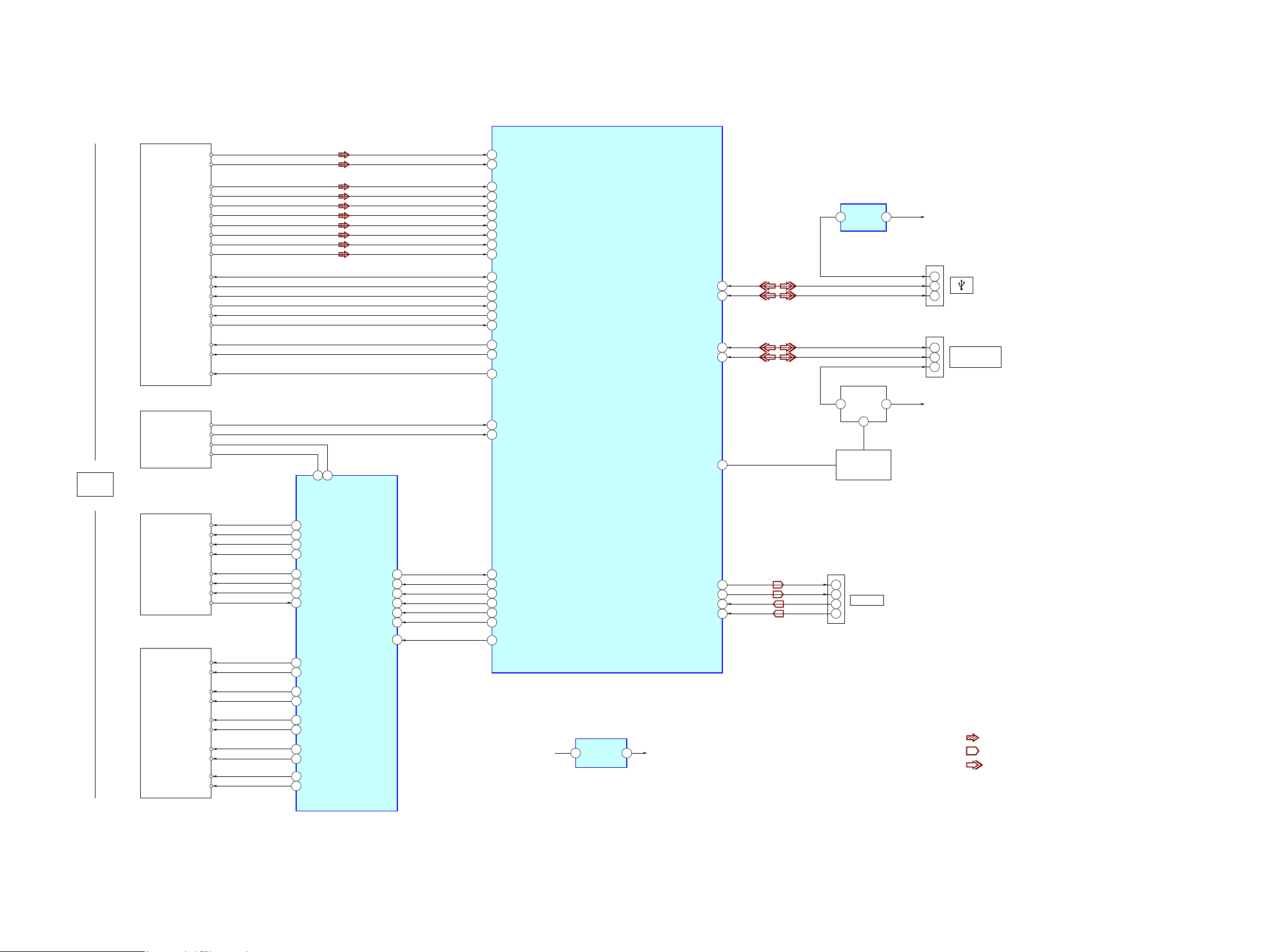
6-1. BLOCK DIAGRAM - SERVO Section -
CN501 (1/2)
RF+
RF-
P18
P19
RFIP
RFIN
BD DECODER
IC101 (1/3)
HBD-E2100/E3100/E3200/E4100/E6100
Ver. 1.5
BD DRIVE
(BPX-7)
CN670
TRAY-OUT
CN660
CN501 (2/2)
SDIO
SCLK
SEN_LDD
TEST_V
THERMO
MODE_A
MODE_B
LDEN
TRAY-IN
LOAD-
LOAD+
COMMON
INAP6B
INBP5A
INCP8D
INDP7C
INE
G
H
F
COIL/MOTOR
DRIVER
LOAD_N
IC601
SCLK
SIMO
SOMI
XRSTIN 19
XFG
RDY
SSZ
12
13
14
15
16
17
27
26
LOAD_P
B
/B
A
/A
W
V
U
1
2
4
5
47
49
SLED1_P
SLED1_N
SLED2_P
SLED2_N
U43
V45
W
MCOM
P12
INF
P11
INGP9E
INH
P10
FECFREQ
P30
FEOSCEN
P28
FECMOD
P31
FPDODVD
P256
HAVCP3VC_PD
AUX1
P14
FEGAINSW1
P32
FEGIO5
P45
FEGIO7
P47
FETRAYIN_
P53
FEGAINSW2
P33
P41
FEFG
P29
FEGAINSW3
P49
FEGIO4
P39
FETRAYPWM
FEFMO
P34
FEFMO2
P35
FEGIO0
P43
USB_DP_P1
USB_DM_P1
USB_DP_P2
USB_DM_P2
CEC
TXVN_0
TXVP_0
TXVP_1
TXVN_1
P56
P55
P205
P204
P201
P213
P214
P212
P211
FRONT USB VBUS
IC406
1 5VOUT IN
WIFI PWR
CONTROL
1
Q405
WIFI PWR
CONTROL DRIVER
Q404
CN380
4
3
LAN (100)
5
6
DCDC5V
CN52
1
3
2
CN404
2
WLAN/BT COMBO
3
4
4
3
DCDC5V
CARD
SA_B+
SA_B-
SA_A+
SA_A-
HBD-E2100/E3100/E4100/E6100
FD1
FR1
FD2
FR2
TR
TD
38
40
35
30
TRK_P37
TRK_N
FCS_P39
FCS_N
TLT_P36
TLT_N
STP1_P33
STP1_N32
STP2_P31
STP2_N
+8V REG
IC520
VCC VO_S
8
6LJQDOSDWK
: DISC PLAY
8.0V12V
2
: LAN
: USB
3737
Page 38
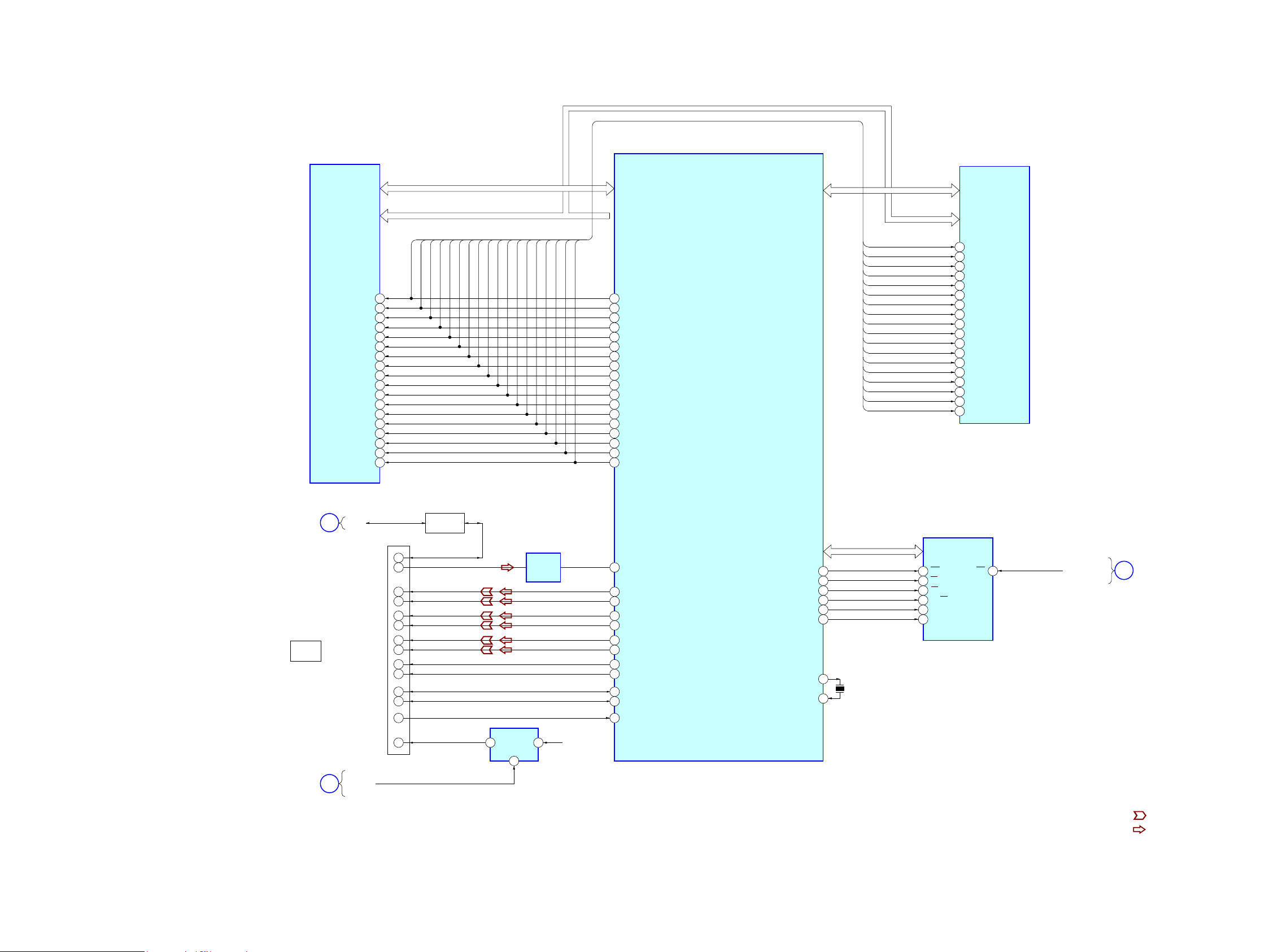
HBD-E2100/E3100/E3200/E4100/E6100
Ver. 1.5
6-2. BLOCK DIAGRAM - MEMORY/HDMI Section -
SD-RAM
IC102
BD DECODER
IC101 (2/3)
SD-RAM
IC103
DQL0 - DQL7,
DQU0 - DQU7
A0 - A13
BA0
BA1
BA2
/WE
/CS
/CAS
/RAS
ODT
CKE
CK
/CK
DMU
DQSU
/DQSU
DML
DQSL
/DQSL
/RESET
M2
N8
M3
L3
L2
K3
J3
K1
K9
J7
K7
D3
C7
B7
E7
F3
G3
T2
D0A0 - D0A13
BA1
BA0
BA2
/WE
/CS
/CAS
/RAS
ODT
CKE
RDQ0 - RDQ15
RA0 - RA13
CK
/CK
DMU
DQSU
/DQSU
DML
DQSL
/DQSL
/RESET
P140
P118
P139
P130
P128
P127
P126
P141
P116
P98
P97
P91
P100
P101
P99
P94
P95
P134
RBA0
RBA1
RBA2
RWE_
RCS_
RCAS_
RRAS_
RODT
RCKE
RCLK0
RCLK0_
RDQM1
RDQS1
RDQS1_
RDQM0
RDQS0
RDQS0_
RRESET
RDQ16 - RDQ31
D0A0 - D0A13
BA0
BA1
BA2
/WE
/CS
/CAS
/RAS
ODT
CKE
CK
/CK
DMU
DQSU
/DQSU
DML
DQSL
/DQSL
/RESET
DQL0 - DQL7,
DQU0 - DQU7
A0 - A13
BA0
M2
BA1
N8
BA2
M3
/WE
L3
/CS
L2
/CAS
K3
/RAS
J3
ODT
K1
CKE
K9
CK
J7
/CK
K7
DMU
D3
DQSU
C7
/DQSU
B7
DML
E7
DQSL
F3
/DQSL
G3
/RESET
T2
MAIN
SECTION
(Page 39)
HDMI
OUT ARC
MAIN
SECTION
(Page 39)
CEC
A
RESERVED (ARC)
TMDS DATA0 +
TMDS DATA0 –
TMDS DATA1 +
TMDS DATA1 –
TMDS DATA2 +
TMDS DATA2 –
TMDS CLOCK +
TMDS CLOCK –
+5V POWER
PCONT3
B
CEC
SDA
SCL
HPD
CN401
13
14
7
9
4
6
1
3
10
12
16
15
19
18
CEC DRIVER
Q401
4
+5V REG
IC408
1
WAVE
SHAPER
IC403
5
UNSW +5.5V
P64
P221
P220
P223
P222
P225
P224
P219
P218
P199
P200
P197
SPDIF_IN1
CH0_P
CH0_M
CH1_P
CH1_M
CH2_P
CH2_M
CLK_P
CLK_M
HDMISD
HDMISCK
HTPLG
NFD0 - NFD7
NFWEN
NFREN
NFCEN
NFRBN
NFALE
NFCLE
NS_XTALI
NS_XTALO
P79
P75
P76
P74
P78
P77
P229
P230
X301
27MHz
IO1 - IO8
18
8
9
7
17
16
NAND FLASH
IC1001
WE
RE
CE
RY/BY
ALE
CLE
WP
19
NAND_RESET
C
SECTION
(Page 39)
6LJQDOSDWK
: VIDEO
: AUDIO
MAIN
HBD-E2100/E3100/E4100/E6100
3838
Page 39
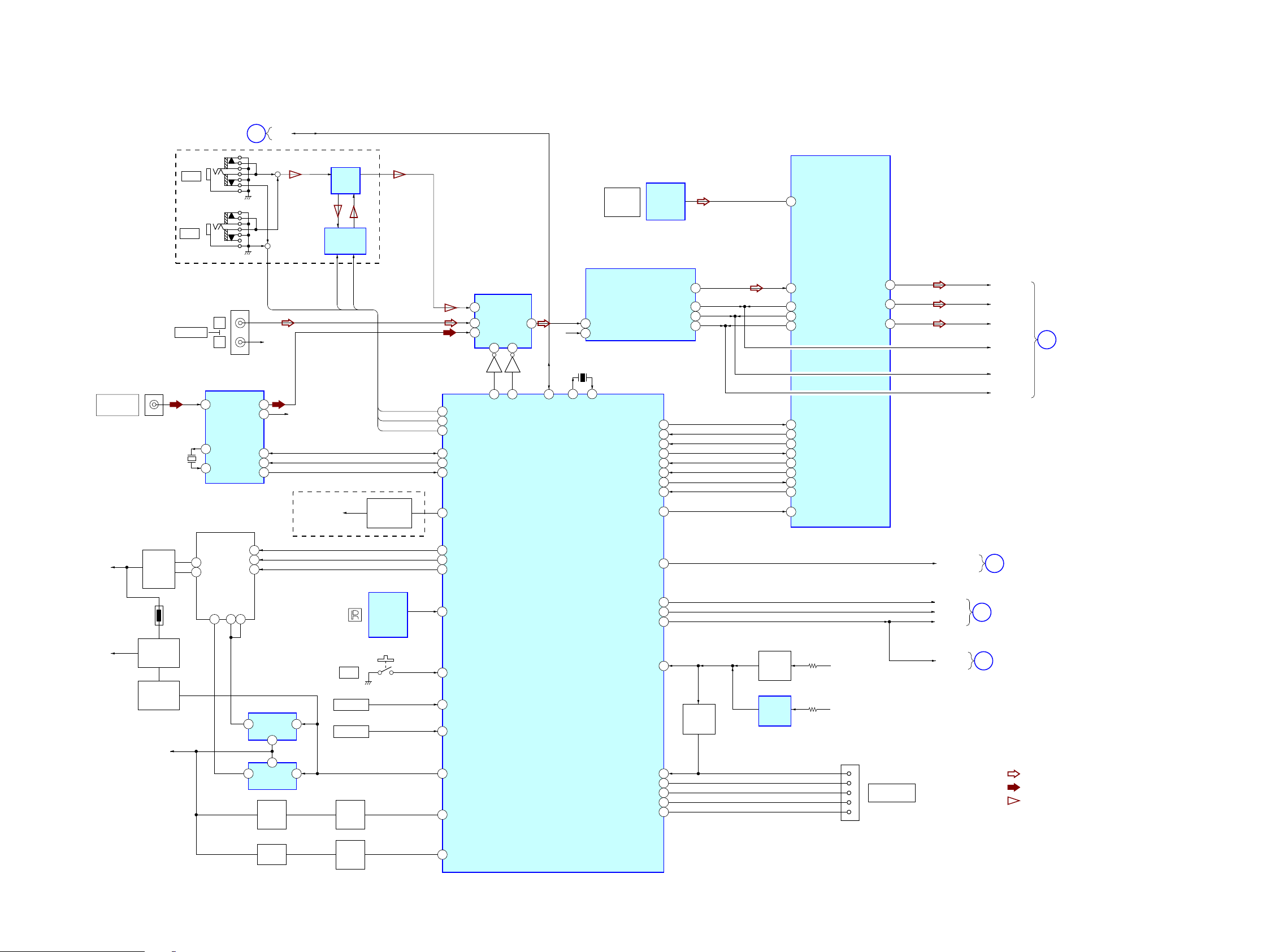
6-3. BLOCK DIAGRAM - MAIN Section -
MEMORY/HDMI
ANTENNA
FM
CN706
J71
MIC 1
J72
MIC 2
SP, RU
AUDIO IN
X701
12MHz
VACUUM FLUORESCENT
SECTION
(Page 38)
L
R
FM DRIVER
(FM RECEIVER)
1FRF1
X2
17
X1
16
ND01
DISPLAY
J702
IC706
CEC
A
+
PLUG_DET
R-CH
13L OUT
12R OUT
11DA
8CK
6IIC/RDSI
+
R-CH
SP, RU
A5V (KARAOKE)
MIC
AMP
IC71
ELECTRICAL
VOLUME
IC72
MIC_CLK
MIC_DATA
MIC_CLK
MIC_DATA
PLUG_DET
OVERLOAD
DETECTION
Q701, Q702
AUDIO SELECT
DRIVER
Q703
MIC CLK
57
58
MIC_DATA
63
PLUG_DET/MIC IN
ST_SDA
45
46
ST_SCL
73
ST_RDS_INT
61
NJU72341_POWER
AUDIO SELECT
2Y2
5Y1
Y0
1
A
10
69
IC703
ASEL0
B
9
70
ASEL1
3Y
R-CH
15
CEC_ TX_RX
DIGITAL IN
OPTICAL
13
VinL
14
VinR
X801
8MHz
11 13
XIN
XOUT
BD_SDI(IF_SDO)(IF_SDO)
BD_SDO(IF_SDI)(IF_SDI)
IC704
BD_CLK
BD_CS
JIG_MODE1
OPWRSB
FE_EJECT
UPG_STATUS
BD_RESET
OPTICAL
RECEIVER
TV
A/D CONVERTER
JACK
IC701
75
76
77
78
82
83
84
85
81
DOUT
SCKI
LRCK
BCK
HBD-E2100/E3100/E3200/E4100/E6100
Ver. 1.5
BD DECODER
IC101 (3/3)
AOSDATA3
P246
P243
9
6
7
8
SPDIF_IN0
P241
AL0
P237
AOLRCK
P242
AR0
P239
P191
P188
P189
P187
P203
P178
P196
P193
VDATA
GPIO0
VCLK
GPIO1
LED0
OPWRSB
TRINAP2
AMUTE
RESET_
AOSDATA0
AOSDATA1
AOSDATA2
P244
P245
AMP_D1
AMP_D2
AMP_D3
AMP_MCK
AMP_LRCK
AMP_BCK
E
AMP
SECTION
(Page 40)
PANEL 12V
FE_SW12V
DISPLAY
DRIVER
TH802
OVERLOAD
DETECTION
OVERLOAD
DETECTION
PANEL 5.5V
SW
Q01
Q803
Q804
21 SW
23 VH
VDD
27 2815
18DIN
19CLK
STB
20
F+
F+
+3.3V REG
3
+3.3V REG
3 1
WHITE_
BT_LED
IC03
IC02
LED
D06
D05
3 FL_DOUT
5 FL_CLK
68 FL_CS
REMOTE
CONTROL
SIGNAL
RECEIVER
IC01
S41
\/1
KEY1
S05 ~ S08
1
4
4
KEY2
S01 ~ S04
LED
DRIVER
Q02
LED
DRIVER
Q03
1
89
88
87
SIRCS_IN
KEY0(EJ)
KEY1_EJ
KEY2_EJ
PCONT_FL25
WHITE_LED24
BT_LED(EJ)26
SYSTEM CONTROLLER
IC801
(1/3)
NAND_RESET
PCONT1
PCONT2 37 PCONT2
PCONT3 38 PCONT3
AC_CUT
RESET
RXD1
ON CHIP DEBUG/CLK1
NO USE/RTS1
TXD1
74
36
AC CUT
18
RESET
DRIVER
Q801
10
30
31
32
29
DRIVER
Q209
VOLTAGE
DETECT
IC803
RESET
RXD1
CLK1
RTS1
TXD1
DCDC +5V
UNSW +12V
CN802
2
4
5
7
8
FLASH
PROGRAMMING
NAND_RESET
PCONT1
PCONT3
MEMORY/HDMI
C
POWER SUPPLY
SECTION
D
(Page 41)
MEMORY/HDMI
SECTION
B
(Page 38)
6LJQDOSDWK
SECTION
(Page 38)
: AUDIO
: TUNER
: MIC
HBD-E2100/E3100/E4100/E6100
3939
Page 40
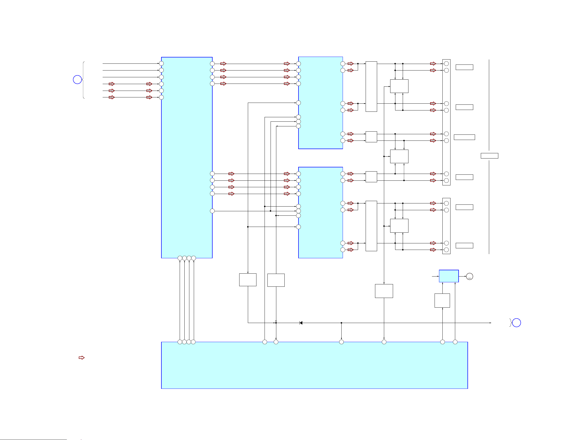
HBD-E2100/E3100/E3200/E4100/E6100
Y
Ver. 1.5
6-4. BLOCK DIAGRAM - AMP Section -
AMP_MCK
E
AMP_LRCK
AMP_BCK
AMP_D1
AMP_D2
AMP_D3
MAIN
SECTION
(Page 39)
11 MCLK
22 LRCK
23 SCLK
SDIN1
24
25
SDIN2
27 SDIN4
STREAM PROCESSOR
IC3001
PWM_P_1
PWM_M_2
PWM_M_8
PWM_P_8
POWER AMP
IC3102
39
40
48
49
29 1N1A OUT1A3016
31
32
23
25
26
27
IN1B
IN2A
1N2B
VL
xPWRDN
xTRISTATE
xFAULT
OUT1A
OUT1B
OUT1B
OUT2B
17
L3101
10
11
3
8OUT2A
L3103
OVERLOAD
DETECTION
Q3101
TB3451
+
+
+
FRONT L
FRONT R
SUBWOOFER
XRESET
XMUTE
19
20 2116
SDA
PWM_M_3
PWM_P_3
PWM_P_5
PWM_M_6
SCL
VAL ID
OVERLOAD
DETECTION
DC
Q3553
Q3202
OVERLOAD
DETECTION
Q3302
FE_UNSW +12V
TB3401
DC FAN
DRIVER
Q208
+
+
+
DC FAN
DRIVER
IC201
CENTER
SUR L
SUR R
POWER AMP
IC3302
42
43
54
55
37
OVERLOAD
DETECTION
Q3552
FAULT
DETECTION
Q3555
29 1N1A
IN1B
30
IN2A
31
1N2B
32
25
xPWRDN
26
xTRISTATE
xFAULT
27
23
VL
OUT1B
OUT1A
OUT2A
OUT2A
OUT2B
OUT2B
11
16
8
9
2
3
L3303
L3301
DETECTION
SPEAKERS
M1
MM
(FAN)
6LJQDOSDWK
HBD-E2100/E3100/E4100/E6100
: AUDIO
51
52
33
TAS5538_XRST
TAS5538_XMUTE
34
TAS5538_SCL
TAS5538_SDA
50
STA516_XPDN
65
D804
SYSTEM CONTROLLER
IC801 (2/3)
DRIVER_SD/POWER_DET
4040
EN_POWER
40
PCONT STA516
35
DC_DET
2 42
FAN_CONT
FAN_ ON
F
SECTION
(Page 41)
POWER SUPPL
Page 41
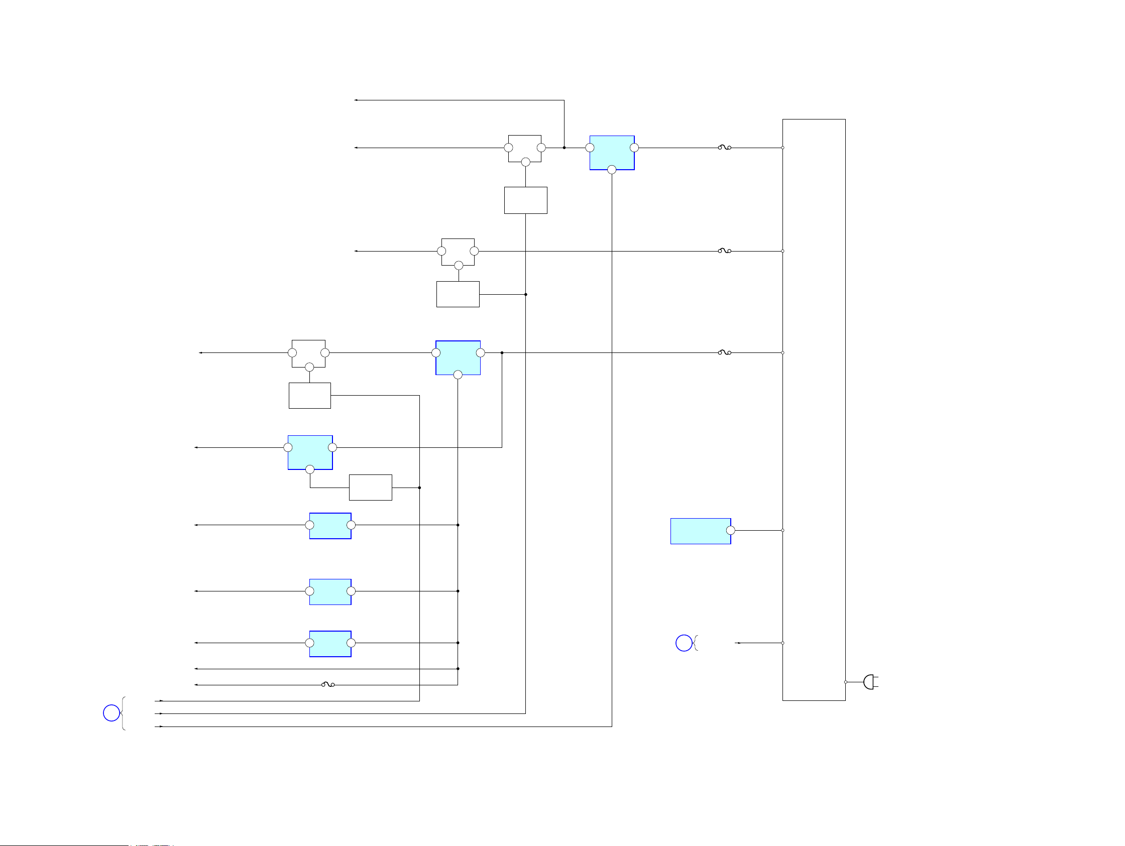
6-5. BLOCK DIAGRAM - POWER SUPPLY Section -
HBD-E2100/E3100/E3200/E4100/E6100
Ver. 1.5
3.3V
3.3V VOLTAGE
CONTROL
Q204
3
OVERLOAD
DETECTION
Q203
DCDC5V
FE_SW5V
FE_SW12V
45
12V VOLTAGE
CONTROL
Q205
45
3
OVERLOAD
DETECTION
Q202
DC-DC CONVERTER
IC203
SW1
VIN1
3
SW2
14
SWR1
SWITCHING
5V VOLTAGE
CONTROL
Q206
45
3
OVERLOAD
DETECTION
Q207
1
DC-DC CONVERTER
IC205
SWENVIN
3
7
2
F202
F203
F201
REGULATOR
UNSW12V
FEUNSW12V
ICUNSW12V
MAIN
SECTION
(Page 39)
D
PCONT3
PCONT2
PCONT1
1.2V
+5V REG
+3.3V REG
+3.3V REG
UNSW 5.5V
PANEL 5.5V
DC-DC CONVERTER
IC204
SW1
VIN1
3
EN2
12
+5V REG
3
IC710
+3.3V REG
4
IC805
+3.3V REG
4
IC804
F802
1
OVERLOAD
DETECTION
Q201
SYSTEM CONTROLLER
IC801 (3/3)
4
5
PVDD_VOL_SEL(EJ)
99
PVDD_CONT
AMP
5
SECTION
(Page 40)
F
EN_POWER
EN_POWER
(AC IN)
HBD-E2100/E3100/E4100/E6100
4141
Page 42
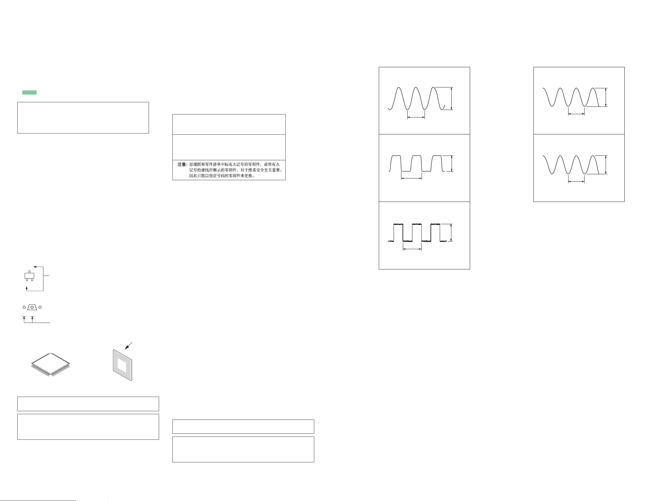
HBD-E2100/E3100/E3200/E4100/E6100
Ver. 1.7
THIS NOTE IS COMMON FOR PRINTED WIRING BOARDS AND SCHEMATIC DIAGRAMS.
(In addition to this, the necessary note is printed in each block.)
For Printed Wiring Boards.
Note:
• X : Parts extracted from the component side.
• Y : Parts extracted from the conductor side.
• f : Internal component.
• : Pattern from the side which enables seeing.
(The other layers' patterns are not indicated.)
Caution:
Pattern face side:
(Conductor Side)
Parts face side:
(Component Side)
• MB1002 board is multi-layer printed board. However, the
patterns of intermediate-layers have not been included in
this diagrams.
• Abbreviation
AR : Argentina model
AUS : Australian model
CH : Chinese model
CND : Canadian model
E3 : 240 V AC area in E model
E12 : 220 – 240 V AC area in E model
E32 : 110 – 240 V AC area in E model
E51 : Chilean and Peruvian models
EA : Saudi Arabia model
MX6 : Latin-American model
PX : PX model
RU : Russian model
SAF : South African model
SP : Singapore model
TH : Thai model
TW : Taiwan model
• Indication of transistor.
C
Q
B
E
Q
B
CE
• Lead layouts
* Replacement of IC102 and IC103 on the MB1002 board used
in this unit requires a special tool.
Note: When the AMP board is replaced, spread the compound
referring to “NOTE OF REPLACING THE IC3102 AND
IC3302 ON THE AMP BOARD AND THE COMPLETE
AMP BOARD” on servicing notes (page 10).
Parts on the pattern face side seen
from the pattern face are indicated.
Parts on the parts face side seen from
the parts face are indicated.
These are omitted.
These are omitted.
surface
CSP (Chip Size Package) Lead layout of conventional IC
For Schematic Diagrams.
Note:
• All capacitors are in μF unless otherwise noted. (p: pF) 50
WV or less are not indicated except for electrolytics and
tantalums.
• All resistors are in Ω and 1/4 W or less unless otherwise
specifi ed.
• f : internal component.
• C : panel designation.
Note: The components identifi ed by mark 0 or
dotted line with mark 0 are critical for safety.
Replace only with part number specifi ed.
Note: Les composants identifi és par une marque
0 sont critiques pour la sécurité.
Ne les remplacer que par une piéce portant
le numéro spécifi é.
• A
• B : B– Line.
• Voltages and waveforms are dc with respect to ground
* : Impossible to measure
• Voltages are taken with VOM (Input impedance 10 M).
Voltage variations may be noted due to normal production
• Waveforms are taken with a oscilloscope.
Voltage variations may be noted due to normal production
• Circled numbers refer to waveforms.
• Signal path.
F : AUDIO
f : TUNER
L : USB
E : VIDEO
d : LAN
J : DISC PLAY
N : MIC
• Abbreviation
AR : Argentina model
AUS : Australian model
CH : Chinese model
CND : Canadian model
E3 : 240 V AC area in E model
E12 : 220 – 240 V AC area in E model
E32 : 110 – 240 V AC area in E model
E51 : Chilean and Peruvian models
EA : Saudi Arabia model
MX6 : Latin-American model
PX : PX model
RU : Russian model
SAF : South African model
SP : Singapore model
TH : Thai model
TW : Taiwan model
• The voltage and waveform of CSP (chip size package)
: B+ Line.
under no-signal conditions.
no mark : TUNER
tolerances.
tolerances.
cannot be measured, because its lead layout is different
from that of conventional IC.
* Replacement of IC102 and IC103 on the MB1002 board used
in this unit requires a special tool.
Note: When the AMP board is replaced, spread the compound
referring to “NOTE OF REPLACING THE IC3102 AND
IC3302 ON THE AMP BOARD AND THE COMPLETE
AMP BOARD” on servicing notes (page 10).
• Waveforms
– MB1002 Board –
1 IC704 6 (SCKI)
40.8 ns
1 V/DIV, 20 ns/DIV
2 IC704 8 (BCK)
20.8 Ps
1 V/DIV, 10 Ps/DIV
3 IC704 7 (LRCK)
40.7 ns
1 V/DIV, 25 ns/DIV
3.3 Vp-p
3.3 Vp-p
3.4 Vp-p
4 IC801 qa (XOUT)
1.7 Vp-p
125 ns
1 V/DIV, 50 ns/DIV
5 IC706 qj (X2)
0.4 Vp-p
83.33 ns
1 V/DIV, 50 ns/DIV
HBD-E2100/E3100/E4100/E6100
4242
Page 43
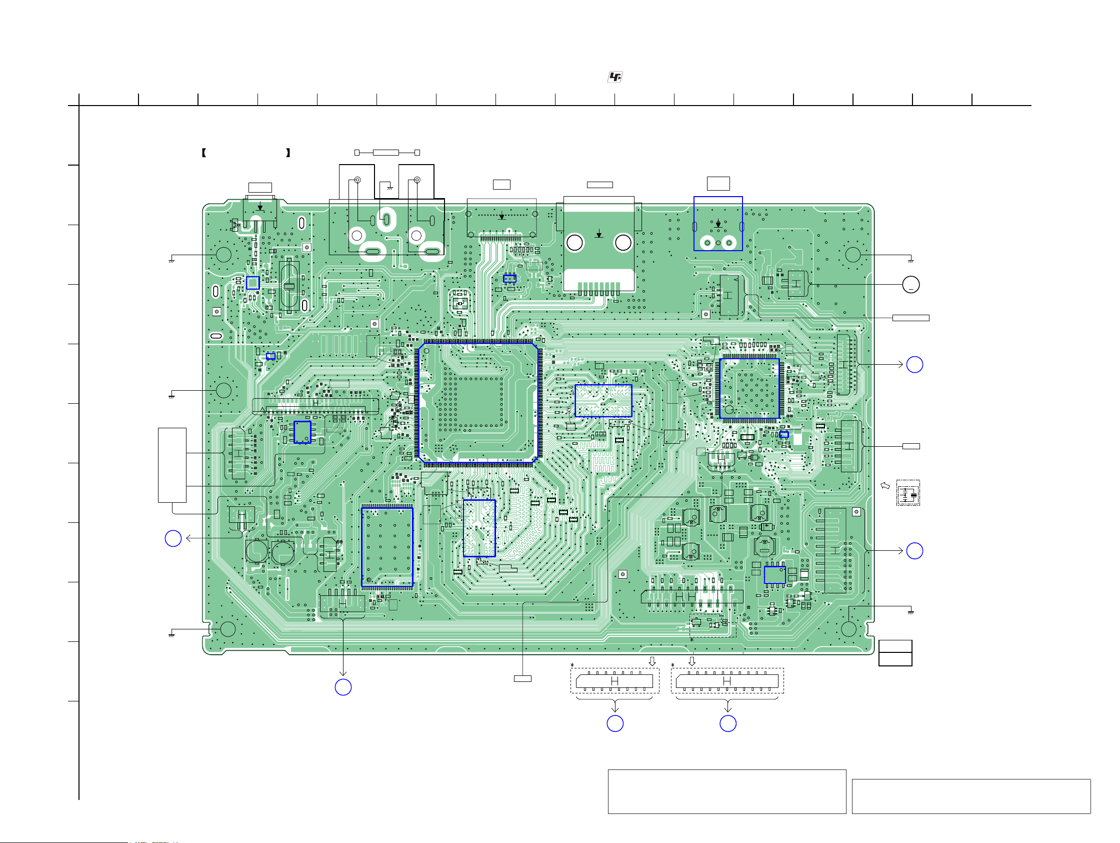
6-6. PRINTED WIRING BOARD - MB1002 Board (Component Side) - • See page 36 for Circuit Boards Location. • : Uses unleaded solder.
HBD-E2100/E3100/E3200/E4100/E6100
Ver. 1.5
1
2 3 4 5 6 7 8 9 10 11 12 13 14 15 16
A
J702
LR
MB1002 BOARD
AUDIO IN
(COMPONENT SIDE)
C350
C172
JL112
C191
C330
IC101
CN401
HDMI
OUT ARC
191
R424
C401
R402
R422
R425
R419
R411
R423
C415
R410
IC408
C414
C408
C353
C352
R365
JL135
JL136
C178
C177
C179
JL198
JL1102
RB101
JL172
JL173
JL114
JL140
JL141
JL175
C190
JL107
JL174
R108
JL196
JL194
JL176
JL177
JL109
JL178
JL108
JL181
JL111
JL110
JL113
JL179
JL180
JL183
JL182
JL184
NFC
SG
Q401
C303
R319
P193P256
P192
JL318
JL319
C186
JL133
JL134
JL120
JL1106
JL121
JL147
C185
C184
JL154
JL131
C183
JL1104
C182
P129
P128
C180
JL142
JL143
RB103
RB104
RB102
R117
CN706
ANTENNA
B
FM
D702
21
R789
L703
L702
CL715
C
(CHASSIS) (CHASSIS)
D
E
(CHASSIS)
F
BD DRIVE
BPX-7
G
A
H
POWER KEY
BOARD
TP41
(Page 58)
C743
L704
C747
C742
C740
CN660
C744
15
6
20
16
10
15
11
CL706
C739
C738
R787
C717
IC710
C718
CL701
C690
CL661
28
CL662
CL663
CL664
CL666
CL667
CL668
CL669
X701
C741
IC706
C751
L707
C737
CL532
CL527
244
1
CL526
CL530
CL531
C6212
C680
C745
R725
R724
C746
R726
R727
R7014
CL703
C721
R575
C575
C577
R522
C523
C521
C643
C646
C647
C603
C601
C600
FB600
C6205
CL536
CL538
CL534
CL537
CL540
CL541
CL539
CL535
R521
R533
R585
C583
C586
C524
C618
C622
C628
CL677
CL678
15
CN670
24
CL675
C426
C428
CN402
CL533
C516
CN501
R531
IC520
C610
C642
C631
R785
R786
R788
19
CN804
I
(CHASSIS)
(CHASSIS)
C730
R581
JL502
JL501
JL504
JL503
JL506
JL508
CL542
CL544
CL546
45
CL616
CL612
CL547
CL543
CL545
JL527
CL614
JL526
C1003
48 25
IC1001
1
15
C1001
R306
JL1009
R1001
C760
C331
C332
C759
R331
X301
R332
CL318
CL509
JL316
C580
C549
CL510
CL548
JL320
R353
JL514
JL512
P1
JL519
P64
P65
C314
JL169
JL167
JL105
JL106
JL1001
JL168
JL164
JL116
JL163
JL162
JL161
JL1014
JL1013
JL1012
R305
C359
JL1101
JL199
JL104
JL103
JL102
C176
JL171
JL101
JL170
JL117
JL166
JL165
A1 A2 A3 A7 A8 A9
B1 B2 B3 B7 B8 B9
C1 C2 C3 C7 C8 C9
D1 D2 D3 D7 D8 D9
JL115
E1 E2 B3 E7 E8 E9
F1 F2 F3 F7 F8 F9
R113
C168
JL139
G1 G2 G3 G7 G8 G9
H1 H2 B3 H7 H8 H9
J1 J2 J3 J7 J8 J9
R111
IC102
K1 K2 K3 K7 K8 K9
L1 L2 L3 L7 L8 L9
JL195
M1 M2 M3 M7 M8 M9
N1 N2 N3 N7 N8 N9
JL138
P1 P2 P3 P7 P8 P9
JL193
R1 R2 R3 R7 R8 R9
T1 T2 T3 T7 T8 T9
JL185
JL197
JL187
RB106
JL186
JL515
CL549
JL518
JL524
R582
JL511
C563
C503
C504
C505
JL507
JL505
C518
C519
C506
C320
JL513
JL522
C533
C311
CL615
C321
C312
JL525
C553
CL673
JL554
R395
C313
C390
C384
JL1007
JL1005
JL1003
JL1006
JL1008
JL1004
JL1002
24
C1002
JL1011
JL1010
J
B
PANEL BOARD
CN51
(Page 56)
K
CN380
LAN (100)
18
C382
JL1105
JL145
JL146
A9
B9
A8
B8
A7
B7
JL119
A3
B3
A2
B2
A1
B1
JL148
JL118
JL1103
JL123
JL149
JL122
R118
RB105
EXCEPT SP, RU SP, RU
C383
C170
R109
R114
JL124
C192
JL144
JL160
C9
D9
E9
G9
F9
H9
J9
K9
C8
D8
E8
G8
F8
H8
J8
K8
C7
D7
E7
G7
F7
H7
J7
K7
IC103
C3
D3
E3
G3
F3
H3
J3
K3
C2
D2
E2
G2
F2
H2
J2
K2
C1
D1
E1
G1
F1
H1
J1
K1
JL125
JL132
JL130
R110
C159
C130
R105
2
CN805
115
R112
C115
JL159
JL157
L9
M9
N9
P9
R9
T9
P8
R8
T8
JL155
P7
R7
T7
JL156
JL191
P3
R3
T3
JL126
P2
R2
T2
JL127
P1
R1
T1
JL153
C193
JL189
JL188
14
JL158
R888
2
12115
L8
M8
N8
L7
M7
N7
L3
M3
N3
L2
M2
N2
L1
M1
N1
JL128
RB112
C
PANEL BOARD
CN02
(Page 56)
TV
DIGITAL IN
OPTICAL
IC701
VCCVOUT GND
C242
JL218
JL219
CN201
JL215
CL854
L207
R211
R840
R847
D220
20
R841
R246
IC205
Q206
CL855
R871
C816
CL844
12
CL843
CL846
CL847
CL845
CL885
CL884
5175
50
CL861
R913
R856
R860
R862
R864
R861
R865
26
CL883
CL878
C812
CL857
IC803
R880
JL826
R886
C269
R275
C244
C245
C251
R215 R216
Q205
C212
C214
1
C430
C427
5
R814
R816
R803
R903
R907
R818
R817
R904
R813
R820
R920
R911
R908
R825
E
Q701
SP, RU
76
CL821
100
125
CL890
CL889
R910
17
CN806
2
L208
L204
R896
R898
R734
R733
Q702 S G
R894
R815
CL808
R819
CL813
R821
R822
R823
CL886
JL192
JL129
JL151
JL152
JL150
JL190
L201
R204
R228
C201
C208
C206
C207
C238
L202
R231
R824
R887
R889
CN805
2
121
L205
CN404
R804
C240
R831
R838
R827
R830
R828
IC801
CL849
C806
C226
C227
R868
CL888
X801
R837
R909
R872
R869
KA
E
D803
Q801
8
R870
C809
R245
C221
C220
L209
L203
C252
C253
R260
2014
CN803
R258 R259
JL221
C818
C719
CN803
D
PANEL BOARD
CN01
(Page 56)
R877
R867
R318
R217
CL865
R761
R760
CL867
R769
R768
R863
C810
L206
E
Q202
R218
FB701
R773
R771
R858
R766
R767
R770
R772
RB301
R307
R308
R386
R387
C811
18
1-886-840-
23
1
CN202
WLAN/BT COMBO CARD
24
CN707
2
CN301
61
13, 21
(13, 21)
M
M1 (FAN)
F
(NC)
X801
E
(CHASSIS)
AMP
BOARD
CN3505
(Page 51)
SWR1
SWITCHING
REGULATOR
(Page 51)
HBD-E2100/E3100/E4100/E6100
Note 1: IC101, IC102, IC103, IC706, IC801 and IC1001 on the
MB1002 board cannot exchange with single. When
these parts on the MB1002 board are damaged, exchange the entire mounted board.
4343
Note 2: When replacing the WLAN/BT COMBO card, refer to
“CHECKING METHOD OF NETWORK OPERATION”
(page 11).
Page 44
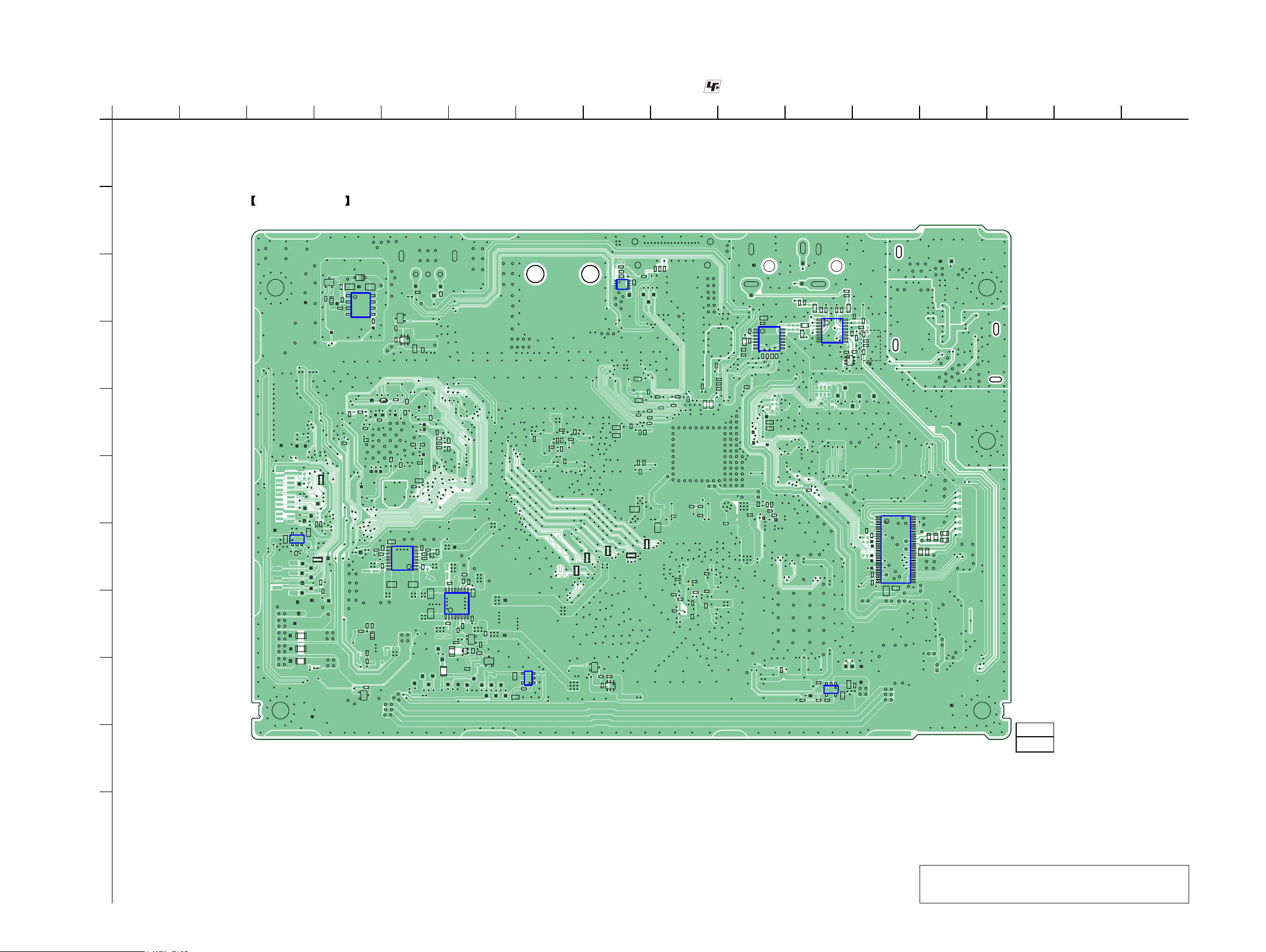
HBD-E2100/E3100/E3200/E4100/E6100
Ver. 1.5
6-7. PRINTED WIRING BOARD - MB1002 Board (Conductor Side) - • See page 36 for Circuit Boards Location. • : Uses unleaded solder.
1
2 3 4 5 6 7 8 9 10 11 12 13 14 15 16
A
MB1002 BOARD
B
C
D
E
F
G
H
I
(CONDUCTOR SIDE)
Q208
R249
E
C241
CL705
JL226
CL704
JL301
JL304
JL315
JL306
JL302
C823
IC805
R918
JL815
JL817
JL819
JL821
JL814
JL208
JL207
F202
JL205
F201
JL204
F203
JL206
R276
R248
R256
R252
JL220
JL216
R850
R855
JL740
RB302
CL856
JL303
R304
R316
C824
JL211
RB802
JL816
JL818
R873
JL820
R874
JL210
JL209
C249
JL225
C410
R455
D202
KA
JL214
C243
IC201
JL217
JL825
R848
R914
CL842
R853
R854
CL853
R244
JL213
C264
C250
C254
C247
R264
R212
Q207
E
CL852
R263
JL718
JL719
C706
CL719
R709
E
Q404
R247
R444
Q405
R443
C431
R445
CL887
R876
R859
D804
CL839
CL882
C807
CL851
C235
R243
C236
C217
R892
R835
R926
IC203
JL827
R810 R811
C804
C822
C216
CL811
R928
CL827
C801
R807
C802
R808
R809
CL879
C803
R927
R219
R268
JL212
R269
C263
R226
C223
R274
C817
JL801
IC204
F802
JL808
R229
C261
C204
JL202
R230
C262
R209
R203
TH802
C805
JL807
JL806
JL201
E
Q201
R210
GS
R901
R900
Q803
E
Q804
JL809
JL810
C813
JL812
JL811
C815
JL886JL887
C205
C257
C259
C237
JL802
JL804
JL885
JL883
JL884
C152
C140
C135
C133
C136
C157
C149
R107
C148
RB111
IC804
R884
R412
R406
IC403
C328
RB110
RB109
Q203
E
C234
R237
R236
Q204
R416
R415
C409
C407
JL403
JL402
CL401
JL401
C360
C361
R385
C380
R780
C326
C327
C188
C141
RB108
C381
R779
R777
R778
R782
R781
C323
C175
R103
C174
C173
C163
RB107
C108
R116
R115
C142
C351
C316
C315
C317
C324
C356
C357
C358
R101
C167
C187
C118
C120
C109
R106
C122
C121
C123
JL715
JL717
C729
C728
C758
R751
C731
R752
R754
C325
JL516
C513
C514
JL520
JL523
JL521
C318
C322
C169
CL317
JL714
JL716
R707
R457
IC704
R749
C440
R456
JL317
C723
C726
R750
R553
C441
R1010
R459
C727
R753
CL402
R708
C713
C714
C715
R716
R717
R718
R719
C716
R739
C722
R738
IC703
C712
C711
R740
R741
R743
R713
R744
R712
SP, RU
Q703
JL592
JL593
JL408
IC406
R434
C423
R431
JL591
CL596
CL597
128
C607
C662
CL601
CL613
CL617
IC601
CL619
CL1200
C629
C630
JL409
JL411
C429
R437
JL410
C424
29 56
C634
C609
CL713
CL714
CL702
R646
R648
R647
R645
R643
R644
JL224
J
K
HBD-E2100/E3100/E4100/E6100
13, 21
1-886-840-
Note: IC203, IC204 and IC601 on the MB1002 board cannot
exchange with single. When these parts on the MB1002
board are damaged, exchange the entire mounted board.
(13, 21)
4444
Page 45
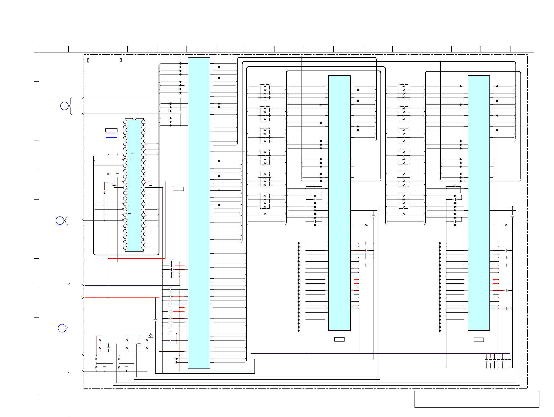
6-8. SCHEMATIC DIAGRAM - MB1002 Board (1/6) - • See page 59 for IC Block Diagrams. • See page 64 for IC Pin Function Descriptions.
HBD-E2100/E3100/E3200/E4100/E6100
Ver. 1.5
A
B
C
D
E
F
G
H
I
J
K
MB1002
BOARD
(3/6)
(Page 47)
MB1002
BOARD
(6/6)
(Page 50)
MB1002
BOARD
(2/6)
(Page 46)
1
1
2
3
2 3 4 5 6 7 8 9 10 11 12 13 14 15 16 17
NFCEN
NFWEN
NAND_RESET
CORE_1.2V
3.3V
DDR_1.5V
GND
MB1002 BOARD (1/6)
C1001
0.001
C1002
C115
1
2
3
4
5
6
3.3
7
3.3
8
3.3
9
10
11
3.3
12
13
0.1
14
15
3.3
16
3.3
17
3.3
18
0.6
19
20
21
22
23
24
0.1
R111
1k
R113
1k
H27U2G8F2CTR-BCR
NFRBN
NFREN
NFCEN
R1001
3.3k
R1010
10k
NFCLE
NFALE
NFWEN
R112
1k
R114
1k
R105
1k
R110
1k
IC1001
IC1001
IC B/D
NAND FLASH
C130
0.1
NC
NC
NC
NC
NC
NC
Y/BY
R
RE
CE
NC
NC
Vcc
Vss
NC
NC
CLE
ALE
WE
WP
NC
NC
NC
NC
NC25NC
15
R1
1k
R116
1k
C168
0.1
NFD7
NFD6
NFD5
NFD4
NFD3
NFD2
NFD1
NFD0
NFRBN
NFREN
NFCEN
NFCLE
NC
48
NC
47
NC
46
NC
45
IO8
44
IO7
43
IO6
42
41IO5
40NC
39
NC
38
NC
37
Vcc
36
Vss
35
NC
34
NC
33
NC
32
IO4
31
IO3
30
IO2
29
IO1
28
NC
27
NC
26
NC
C167
0.1
NFALE
NFWEN
NFD7
1.5
NFD6
1.5
NFD5
3.3
NFD4
3.3
C1003
3.3
0.1
NFD3
3.3
NFD2
3.3
NFD1
3.3
NFD0
3.3
C169 0.1
C172 0.1
C173 0.1
C174 0.1
C175 0.1
C176 0.1
C177 0.1
C178 0.1
C179 0.1
C180 0.1
C182 0.1
C183 0.1
C163
R101
R103
C184 0.1
C185
10
C186 0.1
C187 0.1
C188 0.1
1k
1k
JL1001
JL1002
JL1003
JL1004
JL1005
JL1006
JL1007
JL1008
JL1009
JL1010
JL1011
JL1012
JL1013
JL1014
IC101 (1/3)
CXD90019R-BA
IC101
BD DECODER
0.1
JL135
JL136
P112
P154
P174
P102
P108
P123
P129
P143
P147
P156
P161
P170
P155
P113
P114
P115
P73
P71
P70
P69
P68
P67
P66
P65
P74
P75
P76
P77
P78
P79
P81
P92
P85
P96
P93
NFD7
NFD6
NFD5
NFD4
NFD3
NFD2
NFD1
NFD0
NFRBN
NFREN
NFCEN
NFCLE
NF
ALE
NFWEN
DDRVCCK_1
DDRVCCK_2
DDRVCCK_3
DDRVCCK_4
DDRVCCK_5
DDRVCCIO_1
DDRVCCIO_2
DDRVCCIO_3
DDRVCCIO_4
DDRVCCIO_5
DDRVCCIO_6
DDRVCCIO_7
DDRVCCIO_8
DDRVCCIO_9
DDRVCCIO_A
DDRVCCIO_B
DDRVREF
DDRVREF
AVDD33_MEMPLL
TP_MEMPLL
TN_MEMPLL
RDQ0
RDQ1
RDQ2
RDQ3
RDQ4
RDQ5
RDQ6
RDQ7
RDQ8
RDQ9
RDQ10
RDQ11
RDQ12
RDQ13
RDQ14
RDQ15
RDQM0
RDQS0
RDQS0_
RDQM1
RDQS1
RDQS1_
RCLK0_
RCLK0
RDQ16
RDQ17
RDQ18
RDQ19
RDQ20
RDQ21
RDQ22
RDQ23
RDQ24
RDQ25
RDQ26
RDQ27
RDQ28
RDQ29
RDQ30
RDQ31
RDQM2
RDQS2
RDQS2_
RDQM3
RDQS3
RDQS3_
RCLK1
RCLK1_
RA10
RA11
RA12
RA13
RBA0
RBA1
RBA2
RCKE
RCS_
RCAS_
RRAS_
RWE_
RODT
RRESET
RCSX_
P86
P107
P84
P109
P82
P111
P83
P110
P106
P88
P105
P87
P103
P89
P104
P90
P99
P94
P95
P91
P100
P101
P97
P98
P148
P169
P146
P171
P144
P173
P145
P172
P168
P150
P167
P149
P165
P151
P166
P152
P162
P157
P158
P153
P163
P164
P160
P159
P131
RA0
P120
RA1
P136
RA2
P138
RA3
P1
19
RA4
P137
RA5
P121
RA6
P135
RA7
P122
RA8
P133
RA9
P117
P124
P125
P132
P140
P118
P139
P116
P128
P127
P126
P130
P141
P134
P142
JL198
JL199
JL1101
JL1102
JL1103
JL1104
JL1105
JL1106
D0DQ0
D0DQ1
D0DQ2
D0DQ3
D0DQ4
D0DQ5
D0DQ6
D0DQ7
D0DQ8
D0DQ9
D0DQ10
D0DQ11
D0DQ12
D0DQ13
D0DQ14
D0DQ15
D0DM0
D0DQS0
D0DQS0B
D0DM1
D0DQS1
D0DQS1B
D0DQS2B
D0DQS3B
D0CK0B
D0CK0
D0DQ16
D0DQ17
D0DQ18
D0DQ19
D0DQ20
D0DQ21
D0DQ22
D0DQ23
D0DQ24
D0DQ25
D0DQ26
D0DQ27
D0DQ28
D0DQ29
D0DQ30
D0DQ31
D0DM2
D0DQS2
D0DM3
D0DQS3
D0RRESET
RB101
47
D0CKE_2G
D0A0_2G
D0A10_2G
D0A10
D0BA1
D0A4
RB102
RB103
RB104
RB105
47
RB106
100
47
47
47
D0RRESET_2G
22R117
D0A1
D0A6
D0A8
D0A11
D0A12
D0RAS
D0ODT
D0CAS
D0WE
D0A0
D0A3
D0A13
D0A9
D0RRESET
D0A7
D0A2
D0A5
D0BA2
D0BA0
D0CS
D0CK0
D0CK0B D0CK1B
D0CK1
D0CK1B
D0A0
D0A1
D0A2
D0A3
D0A4
D0A5
D0A6
D0A7
D0A8
D0A9
D0A10
D0A11
D0A12
D0A13
D0BA0
D0BA1
D0BA2
D0CKE
D0CS
D0CAS
D0RAS
D0WE
D0ODT
D0CSX
D0BA1_2G
D0A4_2G
D0A1_2G
D0A6_2G
D0A8_2G
D0A11_2G
D0A12_2G
D0RAS_2G
D0ODT_2G
D0CAS_2G
D0WE_2G
D0A0_2G
D0A3_2G
D0A13_2G
D0A9_2G
D0A7_2G
D0A2_2G
D0A5_2G
D0BA2_2G
D0BA0_2G
D0CS_2G
D0A1_2G
D0A2_2G
D0A3_2G
D0A4_2G
D0A5_2G
D0A6_2G
D0A7_2G
D0A8_2G
D0A9_2G
D0A10_2G
D0A11_2G
D0A12_2G
D0BA0_2G
D0BA1_2G
D0BA2_2G
D0CK0
D0CK0B
D0CKE_2G
D0CS_2G
D0RAS_2G
D0CAS_2G
D0WE_2G
D0RRESET_2G
D0ODT_2G
JL138
JL139
JL140
JL141
JL142
JL143
JL144
JL145
JL146
JL147
JL148
JL149
JL150
JL151
JL152
JL153
JL154
JL155
JL156
JL157
JL158
JL159
JL160
JL161
JL162
D0DM1
D0DQS1
D0DQS1B
D0DM0
D0DQS0
D0DQS0B
JL107
C190
JL108
JL109
JL110
JL111
JL112
C191 100p
JL113
JL197
JL196
JL195
JL194
JL193
JL101
JL102
JL103
JL104
JL105
JL106
N3
A0
P7
A1
P3
A2
N2
A3
P8
A4
P2
A5
R8
A6
R2
A7
T8
A8
R3
A9
L7
A10
R7
A11
N7
A12
M2
BA0
N8
BA1
M3
BA2
D3
DMU
C7
DQSU
B7
/DQSU
E7
DML
F3
DQSL
G3
/DQSL
100R106
J7
CK
K7
/CK
K9
CKE
100p
L2
/CS
J3
/RAS
K3
/CAS
L3
/WE
T2
/RESET
K1
ODT
A9
VSS
B3
VSS
E1
VSS
G8
VSS
J2
VSS
J8
VSS
M1
VSS
M9
VSS
P1
VSS
P9
VSS
T1
VSS
T9
VSS
B1
VSSQ
B9
VSSQ
D1
VSSQ
D8
VSSQ
E2
VSSQ
E8
VSSQ
F9
VSSQ
G1
VSSQ
G9
VSSQ
K4B2G1646Q-BCMA
IC102
SD-RAM
(Chip Size Package)
IC102
*CSP
DQL0
DQL1
DQL2
DQL3
DQL4
DQL5
DQL6
DQL7
DQU0
DQU1
DQU2
DQU3
DQU4
DQU5
DQU6
DQU7
VREFDQ
VREFCA
VDDQ
VDDQ
VDDQ
VDDQ
VDDQ
VDDQ
VDDQ
VDDQ
VDDQ
E3
F7
F2
F8
H3
H8
G2
H7
D7
C3
C8
C2
A7
A2
B8
A3
J1
NC
J9
NC
L1
NC
L9
NC
M7
NC
T7
NC
T3
A13
H1
M8
L8
ZQ
B2
VDD
D9
VDD
G7
VDD
K2
VDD
K8
VDD
N1
VDD
N9
VDD
R1
VDD
R9
VDD
A1
A8
C1
C9
D2
E9
F1
H2
H9
JL114
JL115
JL116
JL117
C118 0.1
C120 0.1
C121 0.1
C122 0.1
C123 0.01
D0DQ0
D0DQ1
D0DQ2
D0DQ3
D0DQ4
D0DQ5
D0DQ6
D0DQ7
D0DQ8
D0DQ9
D0DQ10
D0DQ11
D0DQ12
D0DQ13
D0DQ14
D0DQ15
D0A13_2G
C142
0.1
240R108
D0CKE
D0A10
D0BA1
D0A4
D0A1
D0A6
D0A8
D0A11
D0RAS
D0ODT
D0CAS
D0WE
D0A0
D0A3
D0A13
D0A9
D0RRESET
D0A7
D0A2
D0A5
D0BA2
D0BA0
D0CSX
D0CK1
R118
RB107
RB108
RB109
RB110
RB111
RB112
100
47
47
47
47
47
22
D0CKE_1G
D0A10_1G
D0BA1_1G
D0A4_1G
D0A1_1G
D0A6_1G
D0A8_1G
D0A11_1G
D0A12_1GD0A12
D0RAS_1G
D0ODT_1G
D0CAS_1G
D0WE_1G
D0A0_1G
D0A3_1G
D0A13_1G
D0A9_1G
D0RRESET_1G
D0A7_1G
D0A2_1G
D0A5_1G
D0BA2_1G
D0BA0_1G
D0CSX_1G
D0A0_1GD0CKE
D0A1_1G
D0A2_1G
D0A3_1G
D0A4_1G
D0A5_1G
D0A6_1G
D0A7_1G
D0A8_1G
D0A9_1G
D0A10_1G
D0A11_1G
D0A12_1G
D0BA0_1G
D0BA1_1G
D0BA2_1G
D0CK1
D0CK1B
D0CKE_1G
D0CSX_1G
D0RAS_1G
D0CAS_1G
D0WE_1G
D0RRESET_1G
D0ODT_1G
JL163
JL164
JL165
JL166
JL167
JL168
JL169
JL170
JL171
JL172
JL173
JL174
JL175
JL176
JL177
JL178
JL179
JL180
JL181
JL182
JL183
JL184
JL185
JL186
JL187
D0DM3
D0DQS3
D0DQS3B
D0DM2
D0DQS2
D0DQS2B
JL188
JL189
JL190
JL191
JL192
JL118
JL119
JL120
JL121
JL122
JL123
JL124
C192 100p
JL125
JL126
JL127
JL128
JL129
C193 100p
JL130
100R107
N3
A0
P7
A1
P3
A2
N2
A3
P8
A4
P2
A5
R8
A6
R2
A7
T8
A8
R3
A9
L7
A10
R7
A11
N7
A12
M2
BA0
N8
BA1
M3
BA2
D3
DMU
C7
DQSU
B7
/DQSU
E7
DML
F3
DQSL
G3
/DQSL
J7
CK
K7
/CK
K9
CKE
L2
/CS
J3
/RAS
K3
/CAS
L3
/WE
T2
/RESET
K1
ODT
A9
VSS
B3
VSS
E1
VSS
G8
VSS
J2
VSS
J8
VSS
M1
VSS
M9
VSS
P1
VSS
P9
VSS
T1
VSS
T9
VSS
B1
VSSQ
B9
VSSQ
D1
VSSQ
D8
VSSQ
E2
VSSQ
E8
VSSQ
F9
VSSQ
G1
VSSQ
G9
VSSQ
K4B2G1646Q-BCMA
(Chip Size Package)
IC103
IC103
SD-RAM
*CSP
DQL0
DQL1
DQL2
DQL3
DQL4
DQL5
DQL6
DQL7
DQU0
DQU1
DQU2
DQU3
DQU4
DQU5
DQU6
DQU7
VREFDQ
VREFCA
VDDQ
VDDQ
VDDQ
VDDQ
VDDQ
VDDQ
VDDQ
VDDQ
VDDQ
E3
F7
F2
F8
H3
H8
G2
H7
D7
C3
C8
C2
A7
A2
B8
A3
J1
NC
J9
NC
L1
NC
L9
NC
M7
NC
T7
NC
T3
A13
H1
M8
L8
ZQ
B2
VDD
D9
VDD
G7
VDD
K2
VDD
K8
VDD
N1
VDD
N9
VDD
R1
VDD
R9
VDD
A1
A8
C1
C9
D2
E9
F1
H2
H9
C108 0.1
C157 0.1
C109 0.1
C170 10
JL131
JL132
JL133
JL134
C159
C133 0.01
C135 0.1
C136 0.1
C140 0.1
C141 10
C152 1
C149 1
D0DQ16
D0DQ17
D0DQ18
D0DQ19
D0DQ20
D0DQ21
D0DQ22
D0DQ23
D0DQ24
D0DQ25
D0DQ26
D0DQ27
D0DQ28
D0DQ29
D0DQ30
D0DQ31
D0A13_1G
0.1
240R109
C148 1
HBD-E2100/E3100/E4100/E6100
Note: IC101, IC102, IC103 and IC1001 on the MB1002 board cannot
exchange with single. When these parts on the MB1002 board
4545
are damaged, exchange the entire mounted board.
Page 46
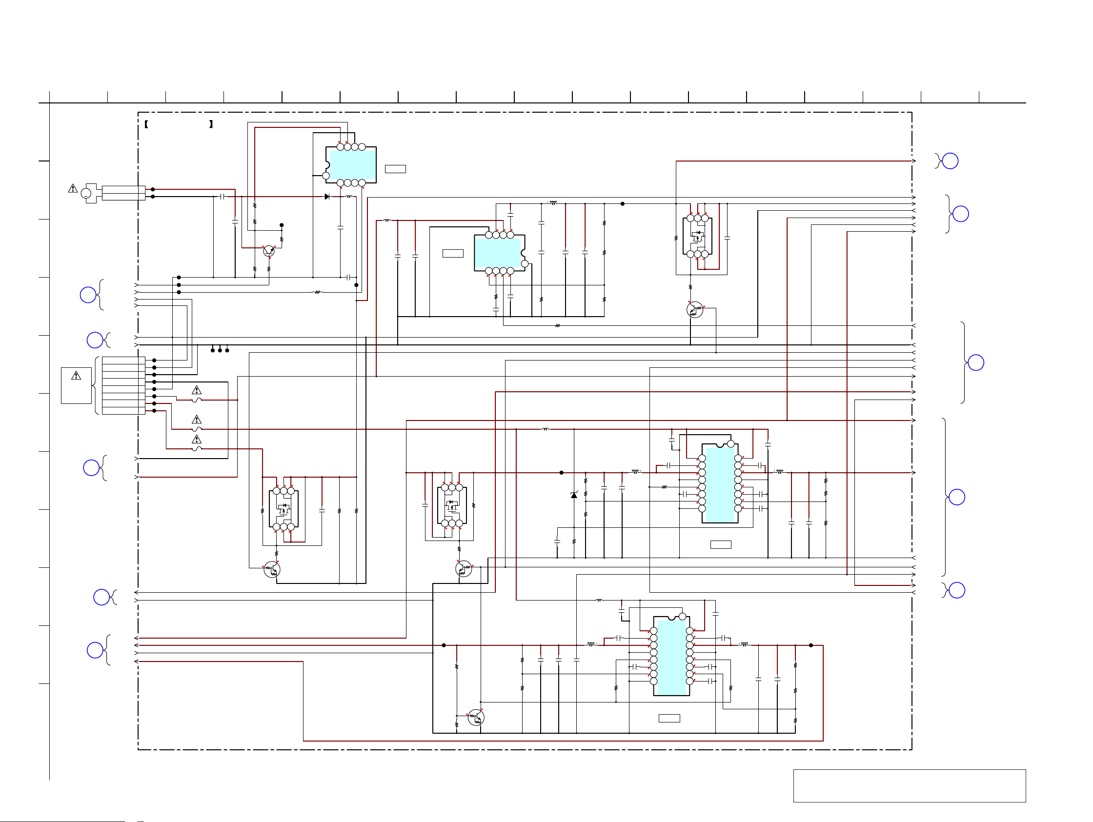
HBD-E2100/E3100/E3200/E4100/E6100
Ver. 1.5
6-9. SCHEMATIC DIAGRAM - MB1002 Board (2/6) -
A
B
C
D
E
F
G
H
I
J
K
M1
(FAN)
MB1002
BOARD
(6/6)
(Page 50)
MB1002
BOARD
(4/6)
(Page 48)
SWR1
SWITCHING
REGULATOR
MB1002
BOARD
(6/6)
(Page 50)
MB1002
BOARD
(5/6)
(Page 49)
MB1002
BOARD
(1/6)
(Page 45)
1
2 3 4 5 6 7 8 9 10 11 12 13 14 15 16 17
MB1002 BOARD (2/6)
5.3
0.8
1234
FB
GND
9
FIN(GND)
N.C
N.C
D202
DA2J10100L
C243
1k
R217
2.2k
VCC VOUT
8765
12
10
JL215
22uH
C240
L205
R218
0.1
2.2k
CN201
2P
2
1
1
2
3
4
5
6
7
8
CN202
8P
JL218
JL219
JL211
JL210
JL209
JL208
JL207
JL205
JL204
JL206
JL214
JL216
JL217
F202 3.15A 32V
3.15A
F201
F203
3.15A
32V
32V
JL226
C242
0.1
C241
JL225
R249
5.6k
R276
R215
JL220
100
R256
1.8k
2.4
5.3
R252
470
33k
2.9
LSCR523UBFS8TL
3
R248
1k
Q205
PMG85XP
12V VOLTAGE
CONTROL
SD D
G
R216
33k
Q208
DC FAN DRIVER
1212
654
DD
123
1261212
0
Q202
LTC014EUBFS8TL
OVERLOAD
DETECTION
R247
C214
0.01
10
JL224
5
3
PVDD_VOL_SEL
ICUNSW12V
7
DC-FAN +
DC-FAN -
FAN_CONT
FAN_O N
EN_POWER
FE_GND_M
GND
EN_POWER
PVDD_CONT
DGND
AGND
FE_GND
UNSW12V
ICUNSW12V
FEUNSW12V
A_GND
3.3VA
GND
3.3V
CORE_1.2V
GND
DDR_1.5V
M
4
(1/3)
6
N.C
EN
3.3
IC201
BD00GA3WEFJ-E2
IC201
DC FAN DRIVER
L206
2.2uH
C244
10
C245
10
C234
0.01
LTC014EUBFS8TL
RT7256ALZSP
IC205
DC-DC CONVERTER
PMG85XP
3.3V VOLTAGE
CONTROL
3.3 3.3
3.3
654
DD
123
3.3
Q203
OVERLOAD
DETECTION
JL201
R210
2.2k
IC205
Q204
3.3 1.4
0
SDD
G
R209
1.5k
R237
0.7
DCDC5V
FE_SW12V
FE_SW5V
FE_GND_M
3.3V
GND
CORE_1.2V
PCONT_WOL_STANDBY
GND
PCONT2
PCONT3
PCONT1
UNSW12V
3.3VA
UNSW5.5V
3.3V
UNSW5.5V
GND
PCONT3
CORE_1.2V
UNSW5.5V
PCONT1
9
R231
4.7k
R230
L207
10uH
C250
0.001
C254
C252
0.001
22
R263
3.3
1kR275
L203
2.2uH
JL212
D220
BZT52H-C6V2
R246
C269
33k
1
L202
2.2uH
C207
C206
22
8.2k
C238
0.01
22
C249
0.1
10
5.5
1234
SW
VIN
GNDFB
BOOT
COMPSSEN
8765
3.6123.3
01
12k
Q201
LTC014EUBFS8TL
OVERLOAD
DETECTION
C251
0.01
R264
C247
2200p
R236
47k
33k
2.9
2.9
C253
R269
R268
R219
JL221
R258
8.2k
R259
47k
22
R260
10k
68k
C226
22
5.6k
22k
L204
C259
2.2uH
10
C237 0.1
R203
1k
C262
0.01
C227
2.2uH
22
L208
Q206
PMG85XP
5V VOLTAGE
CONTROL
1
12
2
5.3
3
1.2
4
5
0
6
0
7
0
8
DC-DC CONVER
R211
33k
Q207
LTC014EUBFS8TL
OVERLOAD
DETECTION
C216
10
C223
R226
1k
C263
0.01
VIN1
VBST1
SW1
PGND1
EN1
SS1
VFB1
GND
IC204
TPS54295PWPR
IC204
0.1
VBST2
PGND2
VREG5
VIN2
VFB2
17
SW2
EN2
SS2
TER
5555
SD D
G
5
R212
33k
0
1
12
2
5.3
3
3.3
4
5
0
6
0
7
0
8
12
16
5.3
15
1.5
14
13
0
12
0
11
0
10
5.6
9
654
DD
123
2.9
17
VIN1
VIN2
VBST1
VBST2
SW1
SW2
PGND1
PGND2
EN1
EN2
SS1
SS2
VFB1
VFB2
GND
VREG5
IC203
TPS54295PWPR
IC203
DC-DC CONVERTER
C257
10
C205
0.1
C261
0.01
C204
1
C212
0.01
GND
R274
C217
10
12
C236
16
0.1
5.3
15
5.5
14
13
0
12
0
11
0
10
5.6
9
L201
2.2uH
1k
C264
C235
L209
2.2uH
0.01
1
C201
22
C208
C220
22
R228
18k
22
R204
3.3k
R229
22k
JL202
C221
JL213
R245
56k
R244
82k
R243
22k
22
MB1002 BOARD
8
(Page 47)
MB1002
BOARD
9
(Page 48)
10
MB1002
BOARD
11
(3/6)
(Page 47)
MB1002 BOARD
12
(3/6)
(4/6)
MB1002
BOARD
(6/6)
(Page 50)
(5/6)
(Page 49)
HBD-E2100/E3100/E4100/E6100
Note: IC203 and IC204 on the MB1002 board cannot exchange
with single. When these parts on the MB1002 board are
4646
damaged, exchange the entire mounted board.
Page 47
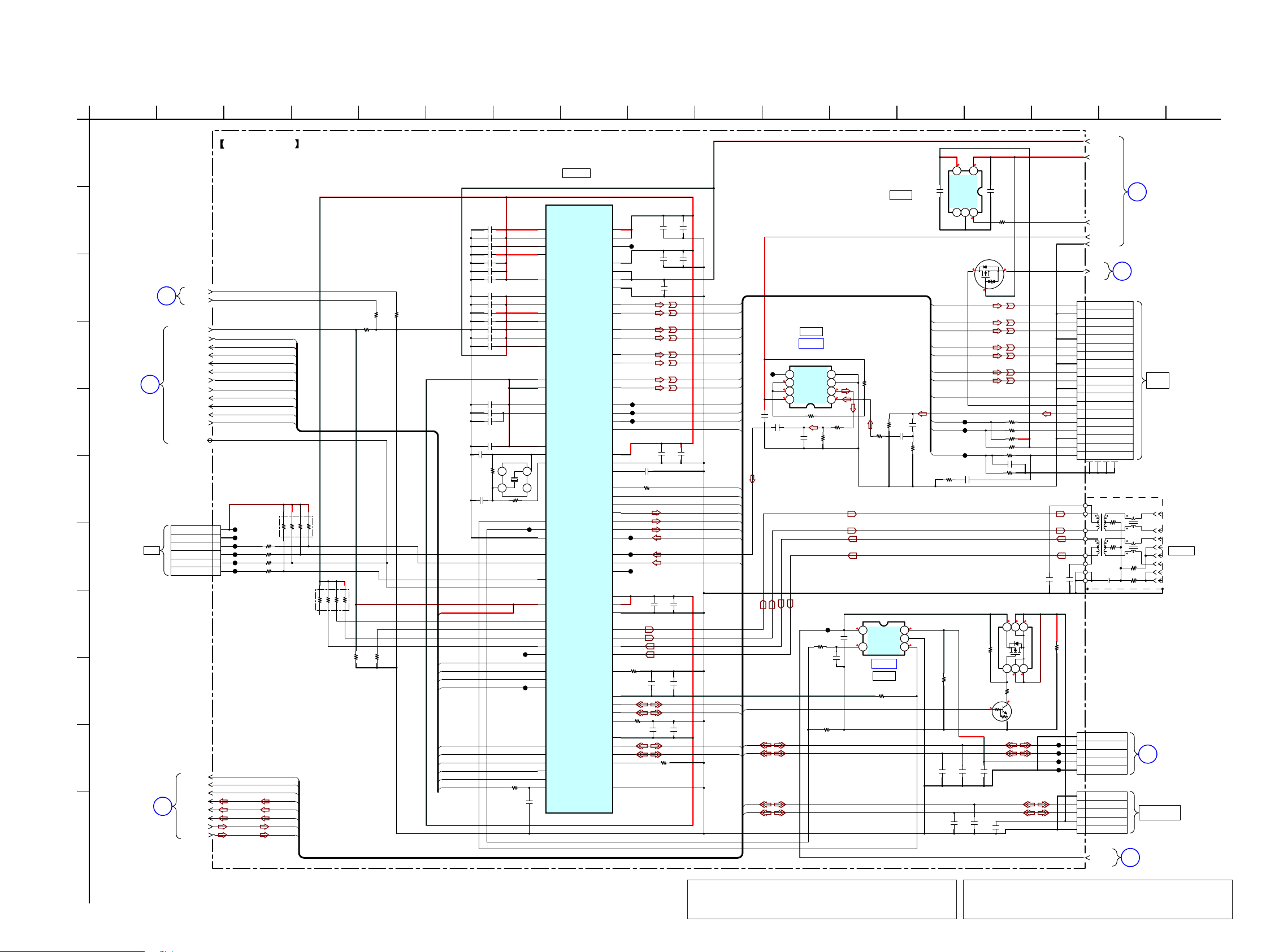
6-10. SCHEMATIC DIAGRAM - MB1002 Board (3/6) - • See page 59 for IC Block Diagrams. • See page 64 for IC Pin Function Descriptions.
HBD-E2100/E3100/E3200/E4100/E6100
Ver. 1.5
A
B
MB1002 BOARD
C
D
MB1002
BOARD
(Page 50)
E
F
G
H
I
J
K
1
(1/6)
(Page 45)
(6/6)
MB1002
BOARD
(5/6)
(Page 49)
13
(NC)
2 3 4 5 6 7 8 9 10 11 12 13 14 15 16 17
CN380
8P
CN402
CN404
5P
5P
CORE_1.2V
UNSW5.5V
PCONT3
3.3V
GND
CEC
1
TMDS DATA2 +
2
TMDS DATA2 SHIELD
3
TMDS DATA2 -
4
TMDS DATA1 +
5
TMDS DATA1 SHIELD
6
TMDS DATA1 -
7
TMDS DATA0 +
8
TMDS DATA0 SHIELD
9
TMDS DATA0 -
10
TMDS CLOCK +
11
TMDS CLOCK SHELD
12
TMDS CLOCK -
13
CEC
14
RESERVED (ARC)
15
SCL
16
SDA
17
DDC/CEC GND
18
+5V POWER
19
HPD
2
3
4
5
6
7
8
1
GND
1
DP
2
DM
3
VBUS
4
SHIELD GND
5
GND
1
DP
2
DM
3
VBUS
4
GND
5
DCDC5V
11
MB1002 BOARD
15
CN401
19P
8
1
14
NFCEN
NFWEN
UNSW3.3V_MTK
SIRCS
UPG_STATUS
WOL_INT
START_BIT
XIF_CS
IF_SDI
OPWRSB
IF_SCK
SYS_REQ
IF_SDO
CPU_XRST
JIG_MODE1
JIG_MODE1
JIG_MODE0
AOMCLK
AOBCLK
AOLRCK
AOSDATA0
AOSDATA1
AOSDATA2
SPDIF_IN
MICIN
MB1002 BOARD (3/6)
CN301
6P
JL301
1
JL302
2
3
4
5
6
JL303
JL304
JL305
JL306
R307
R308
R386
R387
GND
3.3V
RXD
TXD
SIRCS
UPG_STATUS
WOL_INT
START_BIT
XIF_CS
IF_SDI
OPWRSB
IF_SCK
SYS_REQ
IF_SDO
CPU_XRST
100
100
100
100
AOMCLK
AOBCLK
AOLRCK
AOSDATA0
AOSDATA1
AOSDATA2
SPDIF_IN
MICIN
RB301
IC101 (2/3)
CXD90019R-BA
IC101
BD DECODER
DVCC33_IO_1
DVCC33_IO_2
DVCC33_IO_3
DVCC33_IO_4
AVDD12_HDMI_C
DVCC33_IO_7
DVCC12_K_1
DVCC12_K_2
DVCC12_K_3
DVCC12_K_4
DVCC12_K_5
DVCC12_K_6
DVCC12_K_7
DVCC33_IO_STB_1
DVCC33_IO_STB_2
AVDD33_LDO
AVDD12_LDO
A
VDD33_PLLGP
NS_XTALI
NS_XTALO
SCL
SDA
EFPWRQ
UATXD
UARXD
LED1
LED0
AMUTE
GPIO8
GPIO7
GPIO6
GPIO5
GPIO4
GPIO3
GPIO2
GPIO1
GPIO0
AVDD33_USB_P1
AVDD33_USB_P2
OPWRSB
VCLK
VSTB
VDATA
IR
RESET_
AVDD33_VDAC
AVDD33_VDAC
VDACX_OUT
AVDD33_HDMI
AVDD12_HDMI
AVSS12_HDMI
CH2_P
CH2_M
CH1_P
CH1_M
CH0_P
CH0_M
CLK_P
CLK_M
HDMISCK
HDMISD
HTPLG
AVDD33_DAC
AVSS33_DAC
VMID_PWMDAC
AOLRCK
AOSDATA0
AOSDATA1
AOSDATA2
AOSDATA3
SPDIF_IN1
SPDIF_IN0
SPDIF
AVDD33_COM
AVDD33_LD
AVSS33_BG
TXVP_0
TXVN_0
TXVP_1
TXVN_1
REXT
USB_DM_P1
USB_DP_P1
USB_VRT_P1
USB_DM_P2
USB_DP_P2
USB_VRT_P2
EPAD
P232
_BG
P233
_X
P234
CL318
P217
P226
P227
_D
P228
P225
P224
P223
P222
P221
P220
P219
P218
JL401
P200
JL402
P199
JL403
P197
P201
CEC
P236
P238
P235
P237
R353
AL0
P239
AR0
P242
P243
P244
P245
JL320
P246
P64
JL317
P241
P247
JL316
P210
P215
P208
P214
P213
P212
P211
R385
24k
P209
P58
P55
P56
P57
R395
5.1k
P207
P204
P205
P206
P257
X301
27MHz
R332
JL319
1.8k
JL318
CL317
C303
0.001
P36
P46
P61
P72
P240
P27
P42
P60
P80
P175
P216
P248
P184
P198
P176
P177
P231
P229
P230
1
42
P62
P63
P59
P194
P195
P202
P203
P196
P179
P180
P181
P182
P183
P185
P186
P187
P188
P178
P189
P190
P191
P192
P193
100R319
1
0.1C31
0.1C312
0.1C313
0.1C314
0.1C315
0.1C316
0.1C317
0.1C320
0.1C321
C331
C327
C328
C332
0.1C318
0.1C322
0.1C323
0.1C324
0.1C325
0.1C326
1
1
0.1C330
100kR331
10p
3
12p
R306
R305
10k
10k
R304
10k
10k
RB302
10k
R318
R316
10k
100k
UPG_STATUS
WOL_INT
START_BIT
XIF_CS
IF_SDI
OPWRSB
IF_SCK
SYS_REQ
IF_SDO
SIRCS
CPU_XRST
C381
0.1
C351
0.1
C353
0.1
C356
0.1
C358
1
1C359
100
C39010C384
0.1
C361
R365
C380
C350
10
C352
0.1
CH2_P
CH2_N
CH1_P
CH1_N
CH0_P
CH0_N
CLK_P
CLK_N
HDMISCK
HDMISD
HTPLG
WIFI_PCONT
C357
10
AOMCLK
AOBCLK
AOLRCK
AOSDATA0
AOSDATA1
AOSDATA2
SPDIF_IN
MICIN
10
DM1
DP1
C360
0.1
10
5.1k
DM2
DP2
C407
0.1
WIFI_PCONT
DP1
DM1
DP2
DM2
CL401
C441
IC403
TC7WHU04FK
IC403
IC B/D
WAVE SHAPER
2Y
6
7
8
C440
12p
3A
1Y
VCC
GND54
2A
3
1.61.5
3Y
2
1.6
1A
1
10kR406
R457
R456
220
100
CL402
R431
C424
1k
10
C423
0.1
R459
4.7k
3.3
1.5
3.3
0.01
IC408
MM1839A50NRE
IC408
R412
220k
R415
47k
R455
470
IC406
TPS2065CDBVR
51
IN
VOUT
GND
4
FaultEN
+5V REG
C410
C409
0.01
C408
1
LSK3541FS8T2L
CEC DRIVER
CH2_P
CH2_N
CH1_P
CH1_N
CH0_P
CH0_N
CLK_P
CLK_N
HDMISCK
HDMISD
1
R416
68
HTPLG
3.35
2
5.3
3
IC B/D
C426
R437
10k
7p
IC406
FRONT USB VBUS
R434
100k
C427
10p
5
45
Vout
NC
Q401
C415
R425
68
C42810C429
7p
C430
10p
GND
5.2
1
JL401
JL402
JL403
123
5.5
Vin
Cont
R443
5.5
33k
3.2
C431
10
C414
1
R419
1k
3.33.3
22R422
22R423
1.8kR410
1.8kR411
1kR424
0.1C401
47kR402
Q405
PMG85XP
WIFI PWR CONTROL
55
456
S
DDDDG
123
5
5
R444
33k
0
LTC014EUBFS8TL
WIFI PWR
CONTROL DRIVER
DP
DM
VBUS
GND
DP
DM
VBUS
GND
5
Q404
C382
C383
0.1
0.1
R445
10k
JL408
JL409
JL410
JL411
MB1002
BOARD
(2/6)
(Page 46)
(6/6)
(Page 50)
HDMI
OUT ARC
LAN (100)
PANEL
BOARD
A
CN51
(Page 57)
WLAN/BT COMBO
CARD
MB1002 BOARD
(2/6)
(Page 46)
HBD-E2100/E3100/E4100/E6100
Note 1:
4747
IC101 on the MB1002 board cannot exchange with
single. When this part on the MB1002 board is damaged,
exchange the entire mounted board.
Note 2: When replacing the WLAN/BT COMBO card, refer to
“CHECKING METHOD OF NETWORK OPERATION”
(page 11).
Page 48
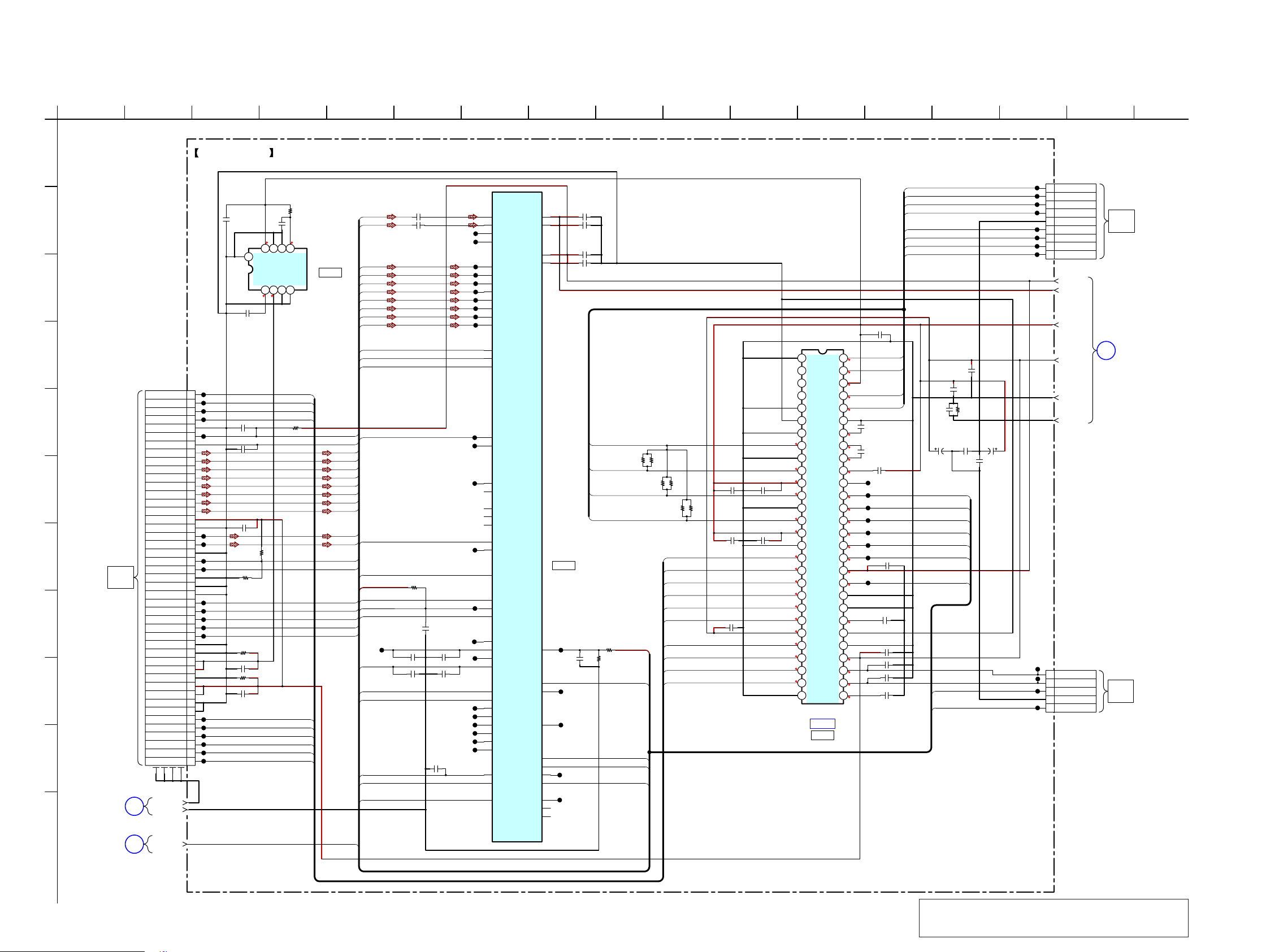
HBD-E2100/E3100/E3200/E4100/E6100
Ver. 1.5
6-11. SCHEMATIC DIAGRAM - MB1002 Board (4/6) - • See page 59 for IC Block Diagrams. • See page 64 for IC Pin Function Descriptions.
A
B
C
D
E
F
G
H
I
J
MB1002 BOARD
K
MB1002 BOARD
1
(2/6)
(Page 46)
(6/6)
(Page 50)
BD DRIVE
BPX-7
(1/3)
2 3 4 5 6 7 8 9 10 11 12 13 14 15 16 17
MB1002 BOARD (4/6)
CN660
CL661
CL662
CL663
CL664
CL666
CL667
CL668
CL669
CL677
CL678
CL673
CL675
9P
CN670
5P
1
2
3
4
5
6
7
8
9
1
2
3
4
5
/A
A
/B
B
FGND
U
V
W
COMMON
3.3V
CORE_1.2V
FE_SW12V
FE_SW5V
FE_GND_M
GND
LOAD-
LOAD+
TRAY-IN
GND
TRAY-OUT
9
5
16
SA_A+
SA_B+
THERMO
VC_PD
5V_PD
MODE_A
MODE_B
SEN_LDD
TEST_V
FE_GND_M
GND
FAST_EJECT
SA_A-
SA_B-
GND
GND
GND
GND
GND
SDIO
SCLK
LDEN
GND
GND
8.0V
8.0V
GND
5.0V
5.0V
GND
GND
FE_SLED_A-
FE_SLED_A+
FE_SLED_B-
1C603
FE_SLED_B+
FE_SLED_B-
FE_SLED_A+
FE_SLED_A-
0.1C610
0.1C622
1C618
1C631
0.01C629
0.01
0.1C628
FE_SLED_B+
FE_SPDL_W
FE_SPDL_V
FE_SPDL_U
FE_SPDL_COM
FG
RDY
SSZ
SCLK
SIMO
SOMI
C600
0.01
C6205
47 16V
FE_GAINSW3
FE_GIO4
FE_TYPWM
FE_FMO
FE_FMO2
FE_MUTE1
FE_TRAYIN
FE_TRAYOUT
C609
C601
FE_FG
10
10
FB600
C690
2.2
C6212
47 16V
0.1
C680
0.1
R522
C521
1
9
FIN
C524
1
CN501
45P
CL526
1
CL527
2
CL530
3
CL531
4
5
6
7
8
E
9
B
10
D
11
F
12
H
13
C
14
A
15
G
16
17
18
RF+
19
RF-
20
21
22
23
NC
24
25
26
27
28
29
30
31
32
33
34
35
36
37
38
39
40
FD1
41
FR1
42
TR
43
TD
44
FD2
45
FR2
CL532
CL533
CL534
CL535
CL536
CL537
CL538
CL539
CL540
CL541
CL542
CL543
CL544
CL545
CL546
CL547
C575 0.1
C577 0.1
C516 0.1
C583 0.1
C586 0.1
R521
47k
33kR531
2.2kR533
4.7kR585
C523
0.1
6NC7NC8
VCC
VOUT2VO_S3GND4NC
1
8128
10k
12
5
EN
FE_CO_A-
FE_CO_A+
FE_CO_B-
FE_CO_B+
10kR575
FE_FR+
FE_FR-
FE_TR+
FE_TR-
FE_TILT+
FE_TILT-
IC520
BD80GA3WEFJ-E2
IC520
+8V REG
FE_GAINSW
FE_LDD_SDIO
FE_LDD_CLK
FE_LDD_SEN
FE_FPDODVD
FAST_EJECT
FE_AUX1
FE_VHAVC
FE_IN_G
FE_IN_A
FE_IN_C
FE_IN_H
FE_IN_F
FE_IN_D
FE_IN_B
FE_IN_E
FE_RFO+
FE_RFO-
FE_GIO5
FE_GIO7
FE_RFO+
FE_RFO-
FE_IN_A
FE_IN_B
FE_IN_C
FE_IN_D
FE_IN_E
FE_IN_F
FE_IN_G
FE_IN_H
FE_LDD_SDIO
FE_LDD_SEN
FE_LDD_CLK
FAST_EJECT
FE_FPDODVD
FE_AUX1
FE_3.3V_D
FE_GAINSW
FE_TRAYOUT
FE_GAINSW3
JL516
FE_VHAVC
FE_FMO
FE_FMO2
FE_TRAYIN
FE_TYPWM
FE_FG
C518
C519 0.1
C514 1
C563 1
C533
0.01
0.1
47kR553
C513 1
C503 0.01
C553
0.01
CL548
CL549
JL501
JL502
CL509
CL510
JL511
JL512
JL515
JL518
JL519
JL520
JL521
JL522
JL523
JL503
JL504
JL505
JL506
JL507
JL508
JL513
JL514
P252
P253
P256
P255
P251
P254
P18
P19
P20
P21
P12
P11
P10
P30
P31
P28
P15
P16
P17
P14
P32
P33
P29
P13
P34
P35
P37
P38
P24
P25
P40
P26
P53
P39
P41
RFIP
RFIN
RFIP2
RFIN2
P6
INA
P5
INB
P8
INC
P7
IND
INE
INF
P9
ING
INH
FECFREQ
FECMOD
FEOSCEN
P2
TRINA
P1
TRINB
VWDC2O
VWDC3O
MPXOUT1
MPXOUT2
MPXOUT3
FPDODVD
FPDOCD
AUX1
FEGAINSW1
FEGAINSW2
FEGAINSW3
VDAC0
V14
FVREF
P3
HAVC
FEFMO
FEFMO2
FEFMO3
FEFMO4
FOO
TRO
FEDMO
TLO
FETRAYIN_
FETRAYPWM
FEFG
AVDD12_1
AVDD12_2
AVDD33_1
AVDD33_3
FEGIO0
FEGIO1
FEGIO3
FEGIO4
FEGIO5
FEGIO6
FEGIO7
FEGIO9
FEGIO10
FEGIO11
RSTI
P249
P22
P4
P23
IC101 (3/3)
CXD90019R-BA
IC101
BD DECODER
P250
MUTE1
P43
P44
P54
P49
P45
P48
P47
P50
P51
P52
C549
C506 0.01
C504 0.01
C505 0.01
JL524
C580
0.1
JL527
JL554
JL525
JL526
0.01
FE_SPDL_COM
FE_SPDL_W
FE_SPDL_V
FE_SPDL_U
R582
5.1k
R581
SLED1_P
56
(N.C)
55
LINFB
54
LIN9VG
53
TEST
52
(N.C)
51
AGND
50
(N.C)
0 (5.2)
49
R648
R647
2.2k
2.2k
R646
R645
2.2k
2.2k
R644
R643
2.2k
2.2k
FE_FR-
FE_FR+
FE_TR-
FE_TR+
FE_TILT+
FE_TILT-
4.7k
FE_3.3V_D
FE_MUTE1
FE_CO_B+
FE_CO_B-
FE_CO_A+
FE_CO_A-
0.001C646
1C647
0.001C642
1C643
1C634
0 (5.2)
12
0 (5.2)
0 (5.2)
12
0
0
0
0
0
0
5.3
0
0
0
0
MCOM
48
PGND_SPM2
47
W
46
P12V_SPM2
45
V
44
PGND_SPM1
43
U
42
P12V_SPM1
41
PGND_1
40
FCS_N
39
FCS_P
38
TRK_N
37
TRK_P
36
TLT_P
35
TL
34
P5V
33
STP1_P
32
STP1_N
31
STP2_P
30
STP2_N
29
(N.C)
TPIC2060ADFDRG4
SLED1_N
P12V_SLD
SLED2_P
SLED2_N
PGND_2
C10V
GPOUT
SCLK
SIMO
SOMI
SIOV
XRSTIN
(N.C)
(N.C)
CV3P3
T_N
AGND/DGND
(N.C)
P5V12L
LOAD_N
LOAD_P
CA5V
IC601
1
0
2
0
3
12
4
0
5
0
6
C607
0.1
7
*1
*1 4.5(10) (SP)
CP1
CP2
CP3
XFG
RDY
SSZ
10 (EXCEPT SP)
8
0
C662
0.1
9
12
10
12 (18.8)
CL601
11
CL612
12
3.3 (1.8)
CL613
13
3.3
CL614
14
3.3 (1.4)
CL615
15
0 (0.8)
CL616
16
0 (0.8)
CL617
17
0
18
3.3
CL619
19
3.3
20
21
22
3.3
23
24
25
5.3
26
0
C630
27
0
28
5.3
IC B/D
IC601
FE_GIO4
FE_GIO5
FE_GIO7
COIL/MOTOR DRIVER
BD DRIVE
BPX-7
(2/3)
MB1002
BOARD
(2/6)
(Page 46)
BD DRIVE
BPX-7
(3/3)
HBD-E2100/E3100/E4100/E6100
Note: IC101 and IC601 on the MB1002 board cannot exchange
with single. When these parts on the MB1002 board are
4848
damaged, exchange the entire mounted board.
Page 49
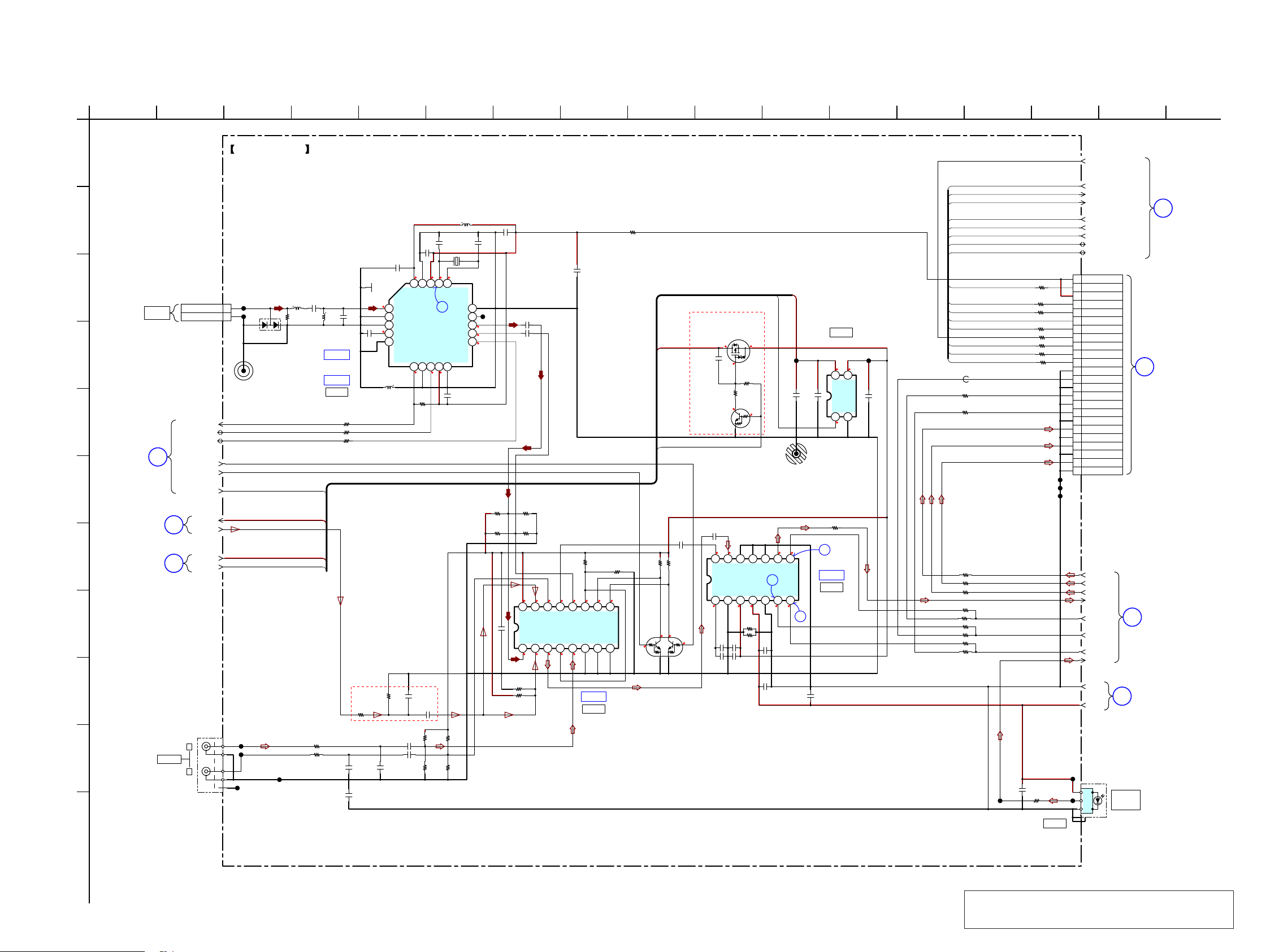
6-12. SCHEMATIC DIAGRAM - MB1002 Board (5/6) - • See page 42 for Waveforms. • See page 59 for IC Block Diagrams.
HBD-E2100/E3100/E3200/E4100/E6100
Ver. 1.5
A
B
C
D
E
F
G
H
I
J
K
1
ANTENNA
MB1002
BOARD
(Page 50)
MB1002 BOARD
(Page 50)
MB1002 BOARD
(Page 46)
(6/6)
(6/6)
(2/6)
17
2 3 4 5 6 7 8 9 10 11 12 13 14 15 16 17
FM
AUDIO IN
I2C_CLK_TUNER
I2C_DATA_TUNER
NJU72341_POWER
18
12
ST_RDS_INT
KA5V_OUT
MIC_SIG
UNSW5.5V
PCONT1
L
WHT
R
RED
MB1002 BOARD (5/6)
CN706
2P
CL713
RF
2
CL714
1
CL715
J702
2P
JL716
1
JL717
2
3
4
G
5
JL714
ASEL1
ASEL0
GND
D702
BAV99-215
L703
47nH
R789
100
NJU72341_POWER
KA5V_OUT
UNSW5.5V
PCONT1
JL715
C743
68p
RN5B701-0001
(EXCEPT AEP, UK)
IC B/D
RN5B701-0002
IC B/D
FM DRIVER
(FM RECEIVER)
22kR707
22kR708
L704
47nH
IC706
(AEP, U K)
IC706
C713
47p
C742
47p
100R786
22R788
22R787
SP, RU
R712
C760
0.1
L707
22nH
C745
C741
3p
2200p
C744
10p
3.3
19
20
GND
L702
22nH
1
2
3
4
5
FRF1
FRF2
GNDRF
CP2
GNDRF
C711
100p
C715 10
C716 10
VDDRF
IIC/RDSI
6
R785
7LA8
10k
C712
0.47
0
0
C747
0.047
R713
4.7k
12k
C714
47p
3.3 0 0
18
VDD
CK
R716
18k
R717
18k
X701
16X117
X2
5
VDD
910
3.33.33.3
KA5V_IN
GND
R718
R719
L OUT
R OUT
18k
18k
CP1
IISD
C740
2200p
12MHz
DA
C751
C746
10
3p
C737
1
15
14
CL706
13
1.5
12
1.5
11
3.3
C738
1
C739
1
R724
R725
47k
47k
R727
R726
47k
47k
5 2.5 2.5 2.5 2.5 2.5 0
14X115
16
X2
VDD
0.1
Y02Y23Y4Y35Y16INH7VEE8VSS
C722
1
2.5 2.5
R738
47k
R739
47k
R740
47k
13
X
IC703
SN74LV4052APWR
2.5 2.5 2.5
11
X312X0
IC B/D
IC703
AUDIO SELECT
R7014
0
SP, RU
KA5V_OUT
LTC014EUBFS8TL
NJU72341_POWER
C726
10
R743
R741
47k
5
9
10
B
A
47k
0
AUDIO SELECT
0
Q703
RN1902
DRIVER
R744
5
47k
3.3
Q702
RTM001P02T2L
OVERLOAD
DETECTION
5
C719
0.01
2.5
R733
R734
33k
0
Q701
OVERLOAD
DETECTION
C723
10
2.5 2.5 1.5 1.6
VinL
FMT
VinR
AGND
AVcc
Vref
2.5 5 3.3 1.6 1.6
C728
C727
0.1
0.1
C729
10
C730
10
PCONT1
UNSW5.5V
5
S
33k
3
MOD1
DVdd
R751
0
C731
R752
0.1
0
C758
10
MOD0
1
DGND
C717
DOUT
SCKI
CL701
10
CL702
891011121314
LRCK BCK
7654321
3
C718
1
A/D CONVERTER
C759
MM3411A50URE
IC710
+5V REG
12
2
IC704
PCM1808PWR
IC B/D
IC704
0.1
IC710
VIN
CE
5.5 5
3.3
100R749
34
VOUT
GND
CL703
C721
1
STA516_TH_WARN
TAS5538_XPDN
DRIVER_SD/PVDD_DETECT
DC_DET
TAS5538_XRST
STA516_XPDN
TAS5538_XMUTE
TAS5538_SCL
TAS5538_SDA
TAS5538_SCL
TAS5538_SDA
TAS5538_XPDN
DRIVER_SD/PVDD_DETECT
DC_DET
TAS5538_XRST
STA516_XPDN
TAS5538_XMUTE
FB701 120ohm
100R760
100R761
100R780
100R781
100R782
22R750
22R777
22R753
22R778
22R754
22R779
CL719
C706
0.1
R766
22
R767
22
R768
100
R769
100
R770
100
R771
100
R772
100
R773
100
JL740
CL704
CL705
R709
100
IC701
OPTICAL RECEIVER
JACK
JL718
JL719
CN707
24P
1
2
3
4
5
6
7
8
9
10
11
12
13
14
15
16
17
18
19
20
21
22
23
24
STA516_TH_WARN
TAS5538_XPDN
DRIVER_SD/PVDD_DETECT
DC_DET
TAS5538_XRST
STA516_XPDN
TAS5538_XMUTE
TAS5538_SCL
TAS5538_SDA
3.3VA
TAS5538_SCL
3.3VA
TASS5538_SDA
TASS5538_XPDN
DRIVE_SD
DC_DET
STA516_TH_WARN
TASS_XRST
STA516_XPDN
TASS5538_XMUTE
DGND
AMP_MCK
DGND
AMP_BCK
DGND
AMP_LRCK
DGND
AMP_D1(FL/FR)
DGND
AMP_D3(C/SW)
DGND
AMP_D2(SL/SR)
DGND
AOSDATA0
AOSDATA1
AOSDATA2
MICIN
AOBCLK
AOMCLK
AOLRCK
SPDIF_IN
GND
3.3VA
1
VCC
2
VOUT
3
GND
4
5
IC701
3P
14
7
TV
DIGITAL IN
OPTICAL
MB1002
BOARD
19
(Page 50)
AMP BOARD
(1/3)
B
CN3505
(Page 53)
MB1002
BOARD
(3/6)
(Page 47)
MB1002 BOARD
(2/6)
(Page 46)
(6/6)
HBD-E2100/E3100/E4100/E6100
Note: IC706 on the MB1002 board cannot exchange with single.
When this part on the MB1002 board is damaged, ex-
4949
change the entire mounted board.
Page 50
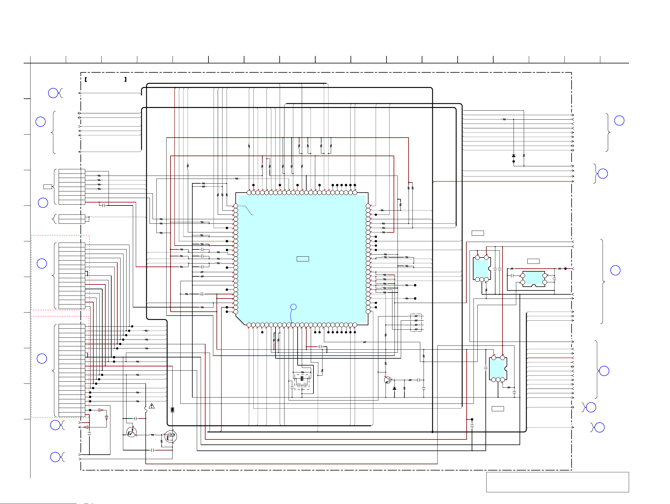
HBD-E2100/E3100/E3200/E4100/E6100
Ver. 1.5
6-13. SCHEMATIC DIAGRAM - MB1002 Board (6/6) - • See page 42 for Waveforms. • See page 64 for IC Pin Function Descriptions.
A
MB1002
BOARD
(1/6)
(Page 45)
B
MB1002
BOARD
(5/6)
(Page 49)
C
D
POWER KEY
BOARD
E
(Page 58)
F
PANEL
BOARD
(Page 57)
G
H
I
PANEL
BOARD
(Page 57)
J
MB1002
BOARD
(5/6)
K
(Page 49)
MB1002
BOARD
(2/6)
(Page 46)
17
C
TP41
D
CN02
E
CN01
1
NFC
2
I2C_DATA_TUNER
I2C_CLK_TUNER
NJU72341_POWER
18
6
NAND_RESET
ST_RDS_INT
ASEL0
ASEL1
RFDET
DATA
SPICLK(clock)
VDD 3.3V
KEY0
KEY0
EXCEPT SP, RU
BT_LED
FL_DOUT
WHITE_LED
FL_CLK
UNSW3.3V
FL_CS
FL_GND
FL_GND
SIRCS_IN
Panel 12V
PCONT_FL
KEY2
Panel 5.5V
KEY1
SP, RU
BT_LED
FL_DOUT
WHITE_LED
FL_CLK
UNSW3.3V
FL_CS
FL_GND
FL_GND
SIRCS_IN
Panel 12V
PCONT_FL
KEY2
Panel 5.5V
KEY1
MIC_DEC
AGND
MIC_SIG
KA5V_OUT
MIC_SIG
A_GND
ICUNSW12V
2 3 4 5 6 7 8 9 10 11 12 13 14 15 16 17
MB1002 BOARD (6/6)
GND
GND
GND
SDA
NAND_RESET
OPWRSB
JIG_MODE1
FAST_EJECT
UPG_STATUS
I2C_DATA_TUNER
I2C_CLK_TUNER
ST_RDS_INT
ASEL0
ASEL1
NJU72341_POWER
CN806
8P
8
7
SW
6
IRQ
5
SEL
4
3
2
1
CN804
2
1
CN805
15P
1
2
3
4
5
6
7
8
9
10
11
12
13
14
15
CN803
21P
1
2
3
4
5
6
7
8
9
10
11
12
13
14
15
16
17
SCL
18
19
20
A5V
21
100R908
R909
100
100R910
R911
100
C822
JL883
JL884
JL885
JL827
C818
0.1
JL802
JL804
JL801
10
JL807
2P
JL808
JL806
JL809
NFC_RFDET
JL811 100R888
JL887
JL810
Q804
LTC014EUBFS8TL
OVERLOAD
DETECTION
C805
JL886
0.1
3.2
NFC_SW
NFC IRQ
NFC SEL
KEY0
100R824
100R825
100R896
100R898
0
KEY2
KEY1
KEY0
NFC SEL
100R889JL812
100R887
F802
1A 50V
R901
10k
C817
0.1
R903
100
R904
100
R803
10k
BT_LED
FL_DOUT
WHITE_LED
FL_CLK
FL_CS
SIRCS_IN
PCONT_FL
KEY2
KEY1
MIC_DATA
PLUG_DET
MIC_CLK
R900
47k
2.1
S
TH802
12
RSM002P03T2L
OVERLOAD
DETECTION
12
10kR807
10kR808
10kR809
R920
Q803
R813
100
10kR894
10kR814
100k
R928
10kR819
10kR820
C801 0.1
C802 0.1
C803 0.1
1kR810
1kR811
10k
C804 0.1
100kR927
SIRCS
XIF_CS
CPU_XRST
100R815
CL886
CL879
CL821
IF_SDI
IF_SCK
100R816
100R817
0
3.3
0
0
CL808
3.3
3.3
3.3
CL811
0
3.3
CL813
3.3
100R821
0
3.3
100R822
3.3
100R823
3.3
0
0
3.3
3.3
3.3
0
3.3
0
CL890
PVDD_VOL_SEL
IF_SDO
NAND_RESET
ST_RDS_INT
100R818
R804
100
CL887
0 3.3 3.3 3.3 0 0 3.3 3.3 3.3 3.3 3.3 0 0 3.3 3.3 3.3 0 0
73
74
75
BD_SDI
(IF_SDO)
(IF_SDO)
76
77
BD_CLK
78
BD_CS
79
NFC DATA
80
NFC SPICLK
81
BD_RESET
82
JIG_MODE1
83
OPWRSB
84
FE_EJECT
85
UPG_STATUS
86
S_AIR_RST (NJ)
87
KEY2_EJ
88
KEY1_EJ
89
KEY0(EJ)
90
DESTINATION(NJ)
91
MODEL
92
DESTINATION(EJ)
93
PCONT_WOL_STANDBY(EJ)
94
AVSS
95
KEY0(NJ)
96
VREF
97
AVCC
98
NFC SEL
99
PVDD_VOL_SEL(EJ)
100
NO USE
ST_RDS_INT
NAND_RESET
BD_SDO(IF_SDI)
(IF_SDI)
SIRCS_IN2FAN_CONT3FL_DOUT4PCONT_TS5FL_CLK6BYTE7CNVSS8NFC_SW9NFC IRQ10RESET11XOUT12VSS13XIN14VCC115CEC_TX_RX16TS INT17KEY INT
1
3.3 3.3 3.3 3.3 3.3 0 1.5 3.3 1.8 1.7 3.3 3.3 3.3 0
SIRCS_IN
FL_DOUT
WOL_INT
10k
R907
71
72
NFC_RFDET
CL889
FL_CLK
ASEL1
ASEL0
1k
R892
69
WOL_WLAN
100kR835
CL827
68
ASEL070ASEL1
100kR926
FL_CS
100k
R827
FL_CS
NFC_SW
STA516_TH_WARN
DRIVER_SD/PVDD_DET
100k
R828
CL882
65
66
67
BD_TEMP(EJ)
STA516_TH_WARN
DRIVER_SD/POWER_DET
R5F3650KCDFB
SYSTEM CONTROLLER
4
X801
C806 0.1
8MHz
NFC IRQ
PLUG_DET
2.2kR831
100R830
63
64
BT_LED(NJ)
PLUG_DET/MIC IN
IC801
IC801
NJU72341_POWER
10kR838
60
61
62
VSS
NJU72341_POWER
C807 0.1
1MR837
MIC_DATA
4.7kR840
CL839
58
59
VCC2
Front_End_Reset
18
CL888
CL849
CEC
MIC_DATA
AC_CUT
R847
27k
MIC_CLK
TAS5538_XMUTE
4.7kR841
CL843
CL842
CL846
CL845
CL844
52
53
54
55
56
57
TS_SCL
NO USE
TS_SDA
MIC CLK
XWAMUTE
BD_IF_REQ(EJ)
TAS5538_XPDN
BD_IF_START(EJ)
PCONT STA516
ON CHIP DEBUG/CLK1
BD_IF_START(NJ)20LED PWM321TS RST22SPK_LED_PWM
CL852
CL853
CL854
23
CL855
BD_IF_REQ (NJ)
24
CL856
WHITE_LED
19
CL851
TAS5538_XRST
CL847
51
_XRST
_XMUTE
TAS5538
TAS5538
STA516
_XPDN
ST_SCL
ST_SDA
NO USE
FAN_O N
NO USE
EPM
PCONT3
PCONT2
PCONT1
DC_DET
TAS5538_SCL
TAS5538_SDA
NO USE/RTS1
RXD1
TXD1
WS_SDA
WS_SCL
BT_LED(EJ)
WHITE_LED25PCONT
_FL
3.3
CL857
PCONT_FL
CE
R868
PCONT_STA516
TAS5538_XPDN
DRIVER_SD/PVDD_DET
FAN_O N
DC_DET
DC_DET
STA516_TH_WARN
TAS5538_XRST
STA516_XPDN
TAS5538_XMUTE
TAS5538_SCL
TAS5538_SDA
FAN_CONT
FAN_O N
IC805
MM1839A33NRE
IC805
+3.3V REG
3.3 5.5
VoutNC
321
JL819
C811
0.1
GND
1.3
54
Vin
Cont
C813 1
STA516_XPDN
TAS5538_XPDN
PVDD_VOL_SEL
R858
R859
4.7k
4.7k
100R848
100R913
100R914
10kR853
10kR854
10kR860
2.2kR861
2.2kR862
47kR863
10kR864
R865
47k
R869
10k
Q801
LSCR523UBFS8TL
RESET DRIVER
0
R850
100k
R873
D803
DA2J10100L
R872
100k
R870
SYS_REQ
START_BIT
I2C_CLK_TUNER
I2C_DATA_TUNER
PCONT_STA516
100kR856
PCONT3
PCONT2
10kR867
PCONT1
TAS5538_SCL
100
JL820
100R874
JL821
RB802
100
R871
10k
47k
C809
0.22
C810
0.01
TAS5538_SDA
FAN_CONT
3.3
50
0.5
49
3.3
CL861
48
0.6
47
3.3
46
3.3
45
3.3
44
CL885
43
3.3
CL865
42
CL884
41
3.3
CL867
40
0
39
R855 3.3k
3.3
38
3.3
37
3.3
36
3.3
35
2.6
34
2.6
33
0
32
0
31
3.3
30
3.3
29
CL883
28
27
CL878
0
26
47k
3.3
BT_LED
RB751S40, 115
1
C8231C824
R918
1k
3.3 5.5
Vout
GND
NC
1.3
IC804
MM1839A33NRE
IC804
+3.3V REG
D804
100R876
R877
1k
JL825
IC803
PST8429UL
VOLTAGE DETECT
3
1.8
4
3.3
IC803
CD
OUT
PCONT1
PCONT2
PCONT3
OPWRSB
XIF_CS
UPG_STATUS
WOL_INT
JIG_MODE1
IF_SCK
IF_SDI
IF_SDO
CPU_XRST
SYS_REQ
START_BIT
SIRCS
CEC
FAST_EJECT
VDD
GND
12
2
1
R880
12k
C812
0.022
54
Vin
Cont
123
R884
1k
C815
1
R886
C816
0.01
33k
JL826
TAS5538_XPDN
DRIVER_SD/PVDD_DETECT
DC_DET
STA516_TH_WARN
TAS5538_XRST
STA516_XPDN
TAS5538_XMUTE
TAS5538_SCL
TAS5538_SDA
EN_POWER
FAN_CONT
FAN_O N
PVDD_VOL_SEL
3.3VA
UNSW5.5V
UNSW12V
GND
PCONT_WOL_STANDBY
PCONT1
PCONT2
PCONT3
UNSW3.3V_MTK
OPWRSB
XIF_CS
UPG_STATUS
WOL_INT
JIG_MODE1
IF_SCK
IF_SDI
IF_SDO
CPU_XRST
SYS_REQ
START_BIT
SIRCS
CEC
FAST_EJECT
MB1002 BOARD
15
16
4
13
19
MB1002
BOARD
(5/6)
(Page 49)
MB1002
BOARD
(2/6)
(Page 46)
10
MB1002
BOARD
(2/6)
(Page 46)
MB1002
BOARD
(3/6)
(Page 47)
(3/6)
(Page 47)
MB1002
BOARD
(4/6)
(Page 48)
HBD-E2100/E3100/E4100/E6100
Note: IC801 on the MB1002 board cannot exchange with single.
When this part on the MB1002 board is damaged, ex-
5050
change the entire mounted board.
Page 51
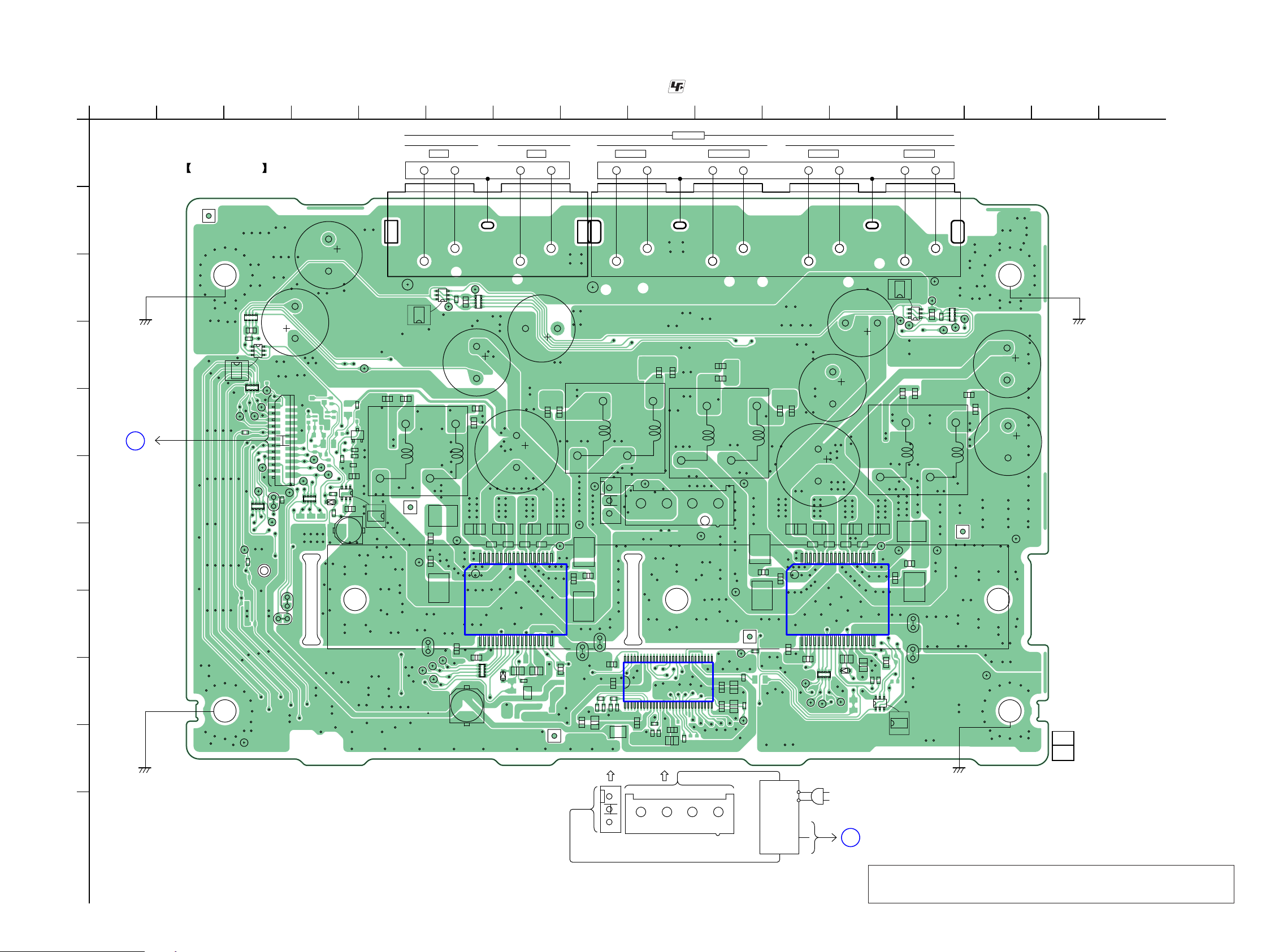
6-14. PRINTED WIRING BOARD - AMP Board (Component Side) - • See page 36 for Circuit Boards Location. • : Uses unleaded solder.
HBD-E2100/E3100/E3200/E4100/E6100
Ver. 1.5
1
A
2 3 4 5 6 7 8 9 10 11 12 13 14 15 16
SPEAKERS
–
+
TB3451
–
–
+
–
+
AMP BOARD
SUR L SUR R
+
TB3401
–
CENTER FRONT L FRONT RSUBWOOFER
–
+
+
(COMPONENT SIDE)
B
C3351
C3136
R3162
C1 B2 E2
C3271
C1 B2 E2
B1E1 C2
TP3104
JL3110
C3117
R3272
C3272
SL3008
SL3010
B1E1 C2
CL3467
Q3101
C3115
R3271
JL3 111
C3127
R3109
TP3105TP3106
TP3102
(CHASSIS)(CHASSIS)
RB3303
TP3103
TP3101
C3122
C3120
EB3008
1-887-311-
(CHASSIS)
C3154
C3152
EB3007
12
(12)
TP3301
R3557
Q3552
CL3410
Q3202
JL3212
B1E1 C2
C1 B2 E2
C3315 C3317
L3301
E
B1 E1C2
C1B2E2
TP3306
TP3046
SL3011
TP3230
TP3045
C3371
R3371
TP3305
C3372
R3372
C
RB3305
SL3000
224
TP3010
SL3001
123
CN3505
R3062
SL3002
C3353
TP3007
TP3001
RB3001
TP3008
R3555
D3503
TP3004
R3556
R3558
TP3002
Q3553
R3560
C3557
R3559
C3555
C3554
C3552
(CHASSIS)
D
E
TP3018
C3328
R3312
B1 E1C2
RB3003
R3073
C1B2E2
TP3020
Q3302
TP3022
TP3019
F
MB1002
BOARD
CN707
F
(Page 43)
G
H
RB3002
TP3015
TP3009
TP3011
R3072
LP3003
I
EB3003
JL3213
R3212
C3228
RB3304
C3352
C3354
C3322
C3320
C3308 C3309 C3118 C3119C3318 C3319
C3356
C3357
118
C3253
C3306 C3307
C3338
JL3303
C3340
IC3302
36 19
C3335
C3050
C3334
RB3302
D3351
C3333
R3032
C3331
R3361
C3336
TP3231
TP3308
SL3009
C3032
L3303
TP3307
C3382
C3381
CL3469
R3382
R3381
C3022
C3339
CN3502
SL3007
C3041
C3341
TP3053
13
C3138
C3140
L3103
CN3001
TP3054
TP3108
2956
IC3001
C3042
C3027 C3028
128
R3024
C3026
R3023
L3051
C3029
C3025
R3041
R3022
R3021
C3033
C3023
R3059
C3031
C3014
C3153
C3251
C3156 C3157
C3151
C3108 C3109
C3106 C3107
L3101
JL3103
C3141
C3139
TP3107
14
R3281
C3281
118
C3282
IC3102
R3282
36 19
RB3102
TP3043
D3151
TP3042
C3133
C3131
R3161
Q3555
C3021
C3013
TP3006
R3033
R3060
R3061
TP3025
C3135
TP3052
C3134
TP3051
J
13
K
CN3502
CN3001
14
SWR1
SWITCHING
REGULATOR
~ AC IN
E
MB1002
BOARD
CN202
(Page 43)
HBD-E2100/E3100/E4100/E6100
Note: When the AMP board is replaced, spread the compound referring to “NOTE OF
REPLACING THE IC3102 AND IC3302 ON THE AMP BOARD AND THE
COMPLETE AMP BOARD” on servicing notes (page 10).
5151
Page 52
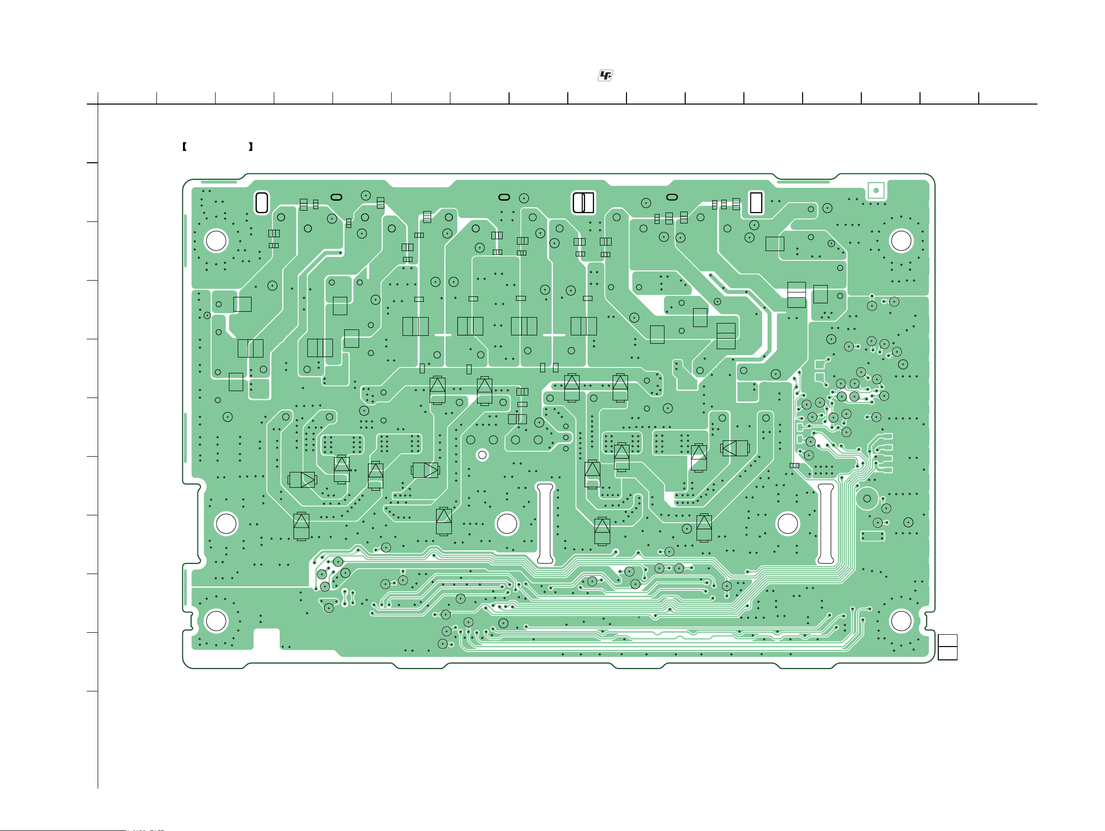
HBD-E2100/E3100/E3200/E4100/E6100
Ver. 1.5
6-15. PRINTED WIRING BOARD - AMP Board (Conductor Side) - • See page 36 for Circuit Boards Location. • : Uses unleaded solder.
1
2 3 4 5 6 7 8 9 10 11 12 13 14 15 16
A
AMP BOARD
(CONDUCTOR SIDE)
JL3470
JL3463
R3153
JL3464
C3452
C3456
C3458
C3457
R3906
C3455
JL3461
TP3201 TP3202
R3902
D3105
JL3462
R3907 R3908 R3909
C3123C3124
R3903
D3106
B
C3460
C
D
EB3001
C3462
JL3465
R3156
C3951 C3952
C3464
C3466
JL3466
C3454
R3155
E
R3154
JL3487
JL3488
F
D3103
D3108
D3102
D3101
G
C3451
C3453
C3099
JL3469
C3463
C3465
C3051
R3051
JL3459
JL3053
TP3203
R3904
JL3460
R3905
TP3204
C3459
C3461
D3305
JL3412
C3401
C3407
C3408
C3405
JL3405
JL3408
C3406
D3306
D3302
JL3406
R3356
R3354
JL3489
D3301
C3323C3324
D3304
C3402
TP3302
C3404
D3307
C3403
TP3304
C3950
JL3407
R3353
TP3303
C3570
C3949
JL3499
JL3501
JL3500
JL3002
JL3004
JL3411
R3355
JL3008
EB3002
JL3026
JL3022
JL3012
JL3013
JL3503
JL3017
JL3313
JL3009JL3010
JL3007
JL3020
JL3015
JL3001
JL3312
JL3019
JL3018
JL3486
JL3011
JL3521
JL3520
JL3485
1-887-311-
12
(12)
D3308
JL3409
JL3481
JL3510
D3104
JL3507
JL3508
D3303
JL3518
JL3476
JL3505
JL3484
D3107
H
I
JL3477
JL3480
JL3479
JL3473
JL3474
JL3506
JL3478
JL3482
JL3504
JL3054
JL3471JL3472
JL3519
J
K
HBD-E2100/E3100/E4100/E6100
5252
Page 53
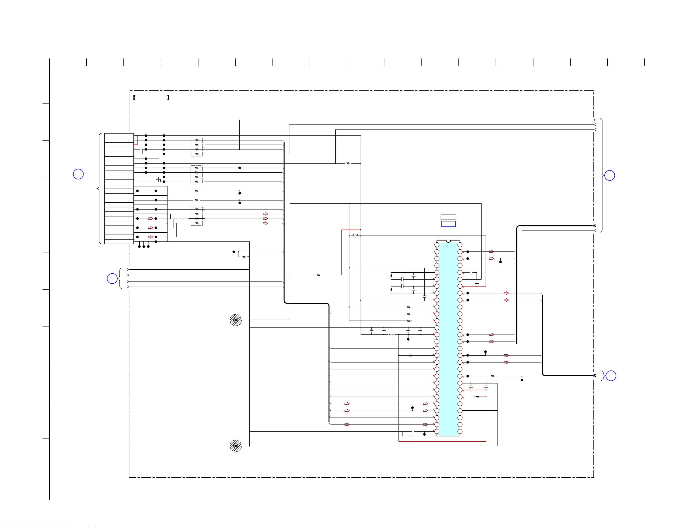
6-16. SCHEMATIC DIAGRAM - AMP Board (1/3) - • See page 59 for IC Block Diagrams.
HBD-E2100/E3100/E3200/E4100/E6100
Ver. 1.5
1
2 3 4 5 6 7 8 9 10 11 12 13 14 15 16 17
A
AMP BOARD (1/3)
5
6
7
AMP BOARD
(2/3)
2
(Page 54)
8
9
AMP BOARD
10
3
(3/3)
(Page 55)
AMP_BCK
AMP_D1
AMP_D3
AMP_D2
AMP_D4
DRIVE_SD
R3032
0
DC_DET
R3062
AMP_MCK
TAS5538_XRST
TAS5538_XPDN
TAS5538_XMUTE
TAS5538_SDA
TAS5538_SCL
AMP_LRCK
AMP_BCK
AMP_D1
AMP_D2
AMP_D4
AMP_D3
10k
IC3001
TAS5538DGGR
IC3001
IC B/D
STREAM
PROCESSOR
C3050
100
6.3V
C3022
R3023
C3028 0.047
470
C3026 0.047
R3024
470
C3032
0.1
10
L3051
10uH
C3023
10
15kR3022
47R3041
18kR3021
C3033
0.1
JL3510
10kR3059
C3014 0.1
C3013
C3029
4700p
C3027
4700p
C3025
JL3508
10
0.1
JL3481
0.6
1.1
1.8
3.3
0.2
1.6
1.1
3.3
3.3
3.3
3.3
3.3
3.3
1.7
1.7
1.8
3
0
0
0
0
PWM_HPM_L
1
PWM_HPP_L
2
PWM_HPM_R
3
PWM_HPP_R
4
AVSS
5
PLL_FLTM
6
PLL_FLTP
7
VR_ANA
8
AVDD
9
ASEL_VACS2
10
MCLK
11
OSC_RES
12
DVSS2_CORE
13
DVDD2_CORE
14
VACS _1
15
XRESET
16
XHP_SEL
17
XPDN
18
XMUTE
19
SDA
20
SCL
21
DVSS1_CORE
LRCK
22
DVDD1_CORE
SCLK
23
SDIN1
24
SDIN2
25
SDIN3
26
SDIN4
27
VR_DIG
28
PWM_P_6
PWM_M_6
PWM_P_5
PWM_M_5
VR_PWM
AVSS_PWM
A
VDD_PWM
PWM_P_8
PWM_M_8
PWM_P_7
PWM_M_7
PWM_P_4
PWM_M_4
PWM_P_3
PWM_M_3
PWM_P_2
PWM_M_2
PWM_P_1
PWM_M_1
VALID
XBKND_ERR
PSVC
TEST
LRCLKO
SCLKO
SDOUT
56
TP3231
55
0
TP3230
54
0
53
C3041
0.1
52
1.8
51
C3042
0.1
50
3.3
TP3052
49
1.6
TP3051
48
1.6
47
46
45
44
TP3046
43
1.6
TP3045
42
1.6
41
40
39
38
37
36
35
34
33
32
31
30
29
JL3507
TP3043
1.6
TP3042
1.6
TP3006
3.3
C3031
0.1
3.3
10kR3060
3.3
R3033
C3021
SR Right +
SR Left -
JL3505
SW -
SW +
Center -
Center +
Right +
Left -
10k
10
JL3519
B
TAS5538_XPDN
C
STA516_TH_WARN
B
MB1002 BOARD
TAS5538 XRST
STA516_XPDN
TAS5538 XMUTE
(5/6)
D
CN707
(Page 49)
AMP_D1(FL/FR)
AMP_D3(C/SW)
E
F
AMP BOARD
(2/3)
(Page 54)
AMP_D2(SL/SR)
1
G
D3.3V
TAS5538_SCL
D3.3V
TAS5538_SDA
DRIVE_SD
DC_DET
DGND
AMP_MCK
DGND
AMP_BCK
DGND
AMP_LRCK
DGND
DGND
DGND
DGND
CN3505
24P
24
23
22
21
20
19
18
17
16
15
14
13
TP3015
12
11
10
9
TP3018
8
7
TP3019
6
5
TP3020
4
3
TP3022
2
1
JL3486
JL3484
1
2
3
4
TP3001
TP3002
TP3004
TP3007
TP3008
TP3009
TP3010
TP3011
JL3485
JL3015
JL3017
JL3018
JL3019
JL3020
JL3022
JL3026
JL3001
JL3002
JL3004
JL3007
JL3008
JL3009
JL3010
JL3011
JL3012
JL3013
RB3001
100
RB3002
100
RB3003
47
TAS5538_SCL
TAS5538_SDA
TAS5538_XPDN
JL3409
47R3072
47R3073
JL3520
JL3521
TP3025
R3061
EB3003
STA516_TH_WARN
TAS5538_XRST
TAS5538_XMUTE
STA516_XPDN
AMP_MCK
AMP_LRCK
10k
STA516_TH_WARN
STA516_XPDN
H
I
J
EB3008
K
HBD-E2100/E3100/E4100/E6100
5353
Page 54
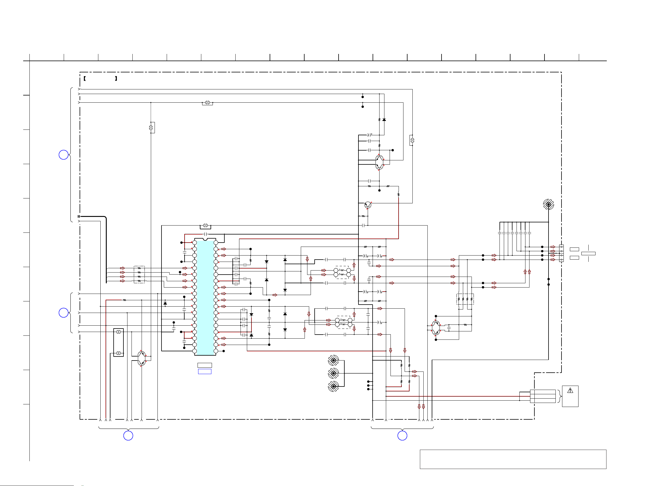
HBD-E2100/E3100/E3200/E4100/E6100
Ver. 1.5
6-17. SCHEMATIC DIAGRAM - AMP Board (2/3) - • See page 59 for IC Block Diagrams.
1
A
2 3 4 5 6 7 8 9 10 11 12 13 14 15 16 17
AMP BOARD (2/3)
7
5
6
SL3001
JL3501
JL3503
DC_DET
PVDD_DET
B
R3555
47k
SL3002
C
AMP
BOARD
(1/3)
2
C3552
47 4V
C3570 1
C3554 0.01
(Page 53)
D
E
F
G
AMP
BOARD
H
(1/3)
(Page 53)
I
J
8
9
JL3471
C3334
0.1
RB3302
SR Right +
SR Left -
Center -
Center +
3
4
1
2
1
SL3009
SL3011
47
10kR3361
3.3
0
0
Q3555
3.3
HN1A01FU
FAULT
DETECTION
JL3472
JL3504
D3351
RB751S40, 115
JL3474
C3331
10
JL3473
C3333
C3336
0.1
JL3476
10
JL3518
SL3007
C3335
54
VCC_SIGN
36
GND_SUB
54
VCC_SIGN
35
VSS
34
VSS
33
1.6
1N2B
32
1.6
IN2A
31
1.6
IN1B
30
1.6
1N1A
29
3.3
TH_WARN
28
3.3
xFAULT
27
3.3
xTRISTATE
26
3.3
xPWRDN
25
CONFIG
24
3.3
VL
23
5
VDD
22
5
VDD
21
GND_REG
20
GND_CLEAN
19 18
IC3302
STA516BF13TR-A
IC3302
IC B/D
POWER AMP
0.1
OUT2B
OUT2B
VCC2B
GND2B
GND2A
VCC2A
OUT2A
OUT2A
OUT1B
OUT1B
VCC1B
GND1B
GND1A
VCC1A
OUT1A
OUT1A
1
2
0
3
C3356
27
0.1
4
32.5
C3308
2.2
5
6
C3309
2.2
7
C3357
32.5
0.1
8
27
9
27
10
27
11
27
12
32.5
13
14
15
32.5
16
27
17
27
N.C
JL3303
C3306
C3318
C3319
2.2
C3307
TP3305
R3371
C3371
330p
22
C3372
330p
R3372
22
TP3306
0.1
2.2
0.1
STPS1H100A
STPS1H100A
D3305
D3306
STPS1H100A
STPS1H100A
TP3307
R3381
C3381
C3382
R3382
TP3308
D3301
D3302
22
330p
330p
22
D3307
STPS1H100A
D3308
STPS1H100A
D3303
STPS1H100A
D3304
STPS1H100A
C3315
C3320
C3338
C3339
EB3002
EB3007
EB3001
C3317
1000p
0.1
3214
L3301
20uH
C3322
0.1
1000p
C3340
1000p
0.1
L3303
20uH
3
C3341
0.1
1000p
C3555 0.1
1kR3559
JL3499
3.3
LSCR523UBFS8TL
0
DC DETECTION
R3560
100k
C3557
0.01
R3353
4.7k
C3351
560 35V
C3949
0.47
C3950
0.47
C3352
560 35V
R3354
4.7k
C3323
0.47
21
4
C3324
0.47
JL3487
JL3488
JL3489
RB751S40, 115
R3556
22k
0
1.2
3.3
0
OVERLOAD DETECTION
R3558
10k
Q3553
R3355
4.7k
C3353
560 35V
C3354
560 35V
R3356
4.7k
C3253
270 63V
D3503
JL3500
Q3552
XP4501
Center -
R3908
33k
R3904
33k
R3557
47k
Center +
SL3000
HN1A01FU
OVERLOAD
DETECTION
R3909
33k
R3905
33k
Q3302
0
0
JL3313
27
27
JL3312
SR Left -
SR Left +
SR Right -
SR Right +
27
27
C3328
CL3410
C3402 1000p
SL +
TP3304
SL -
TP3303
SR +
TP3302
SR -
TP3301
RB3305
100k
R3312
100k
2.2
CN3502
3P
1
2
3
JL3405
JL3406
JL3407
JL3408
JL3412
JL3411
MON GND
MON PVDD
MON GND
C3407 0.01
C3408 1000p
C3405 0.01
C3406 1000p
C3403 0.01
C3404 1000p
C3401 0.01
TB3401
2P
1
+
SUR R
2
3
4
-
+
SUR L
-
SWR1
SWITCHING
REGULATOR
(2/3)
SPEAKERS
5
K
HBD-E2100/E3100/E4100/E6100
11 18 19 20 21 22 2312 13 14 15 16 17
4
AMP BOARD
(3/3)
(Page 55)
C +
C -
5
AMP BOARD
(3/3)
(Page 55)
5454
Note: When the AMP board is replaced, spread the compound referring to “NOTE OF
REPLACING THE IC3102 AND IC3302 ON THE AMP BOARD AND THE
COMPLETE AMP BOARD” on servicing notes (page 10).
Page 55
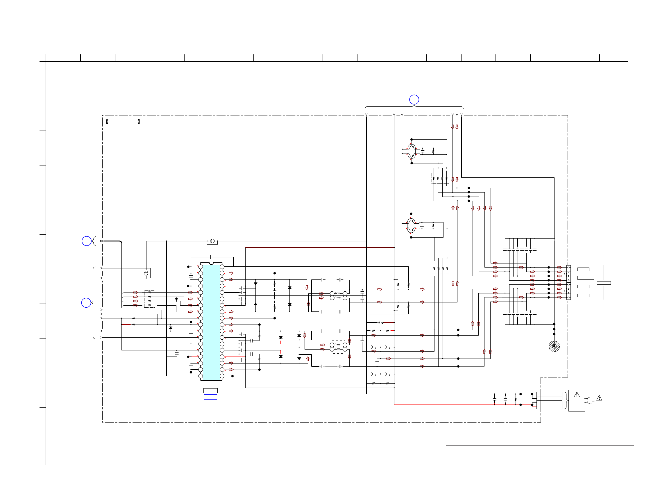
6-18. SCHEMATIC DIAGRAM - AMP Board (3/3) - • See page 59 for IC Block Diagrams.
HBD-E2100/E3100/E3200/E4100/E6100
Ver. 1.5
A
B
C
D
E
F
G
H
I
J
1
AMP BOARD
(1/3)
(Page 53)
AMP BOARD
(2/3)
(Page 54)
2 3 4 5 6 7 8 9 10 11 12 13 14 15 16 17
AMP BOARD
(2/3)
(Page 54)
5
18 19 20 2122 23
C +
R3212
100k
R3109
100k
C -
TP3104
TP3103
TP3101
TP3102
SW +
SW -
TP3204
TP3203
TP3202
TP3201
FL +
FL -
FR -
FR +
SW -
SW +
C -
C +
C3463 0.01
C3465 1000p
C3459 0.01
C3461 1000p
C3455 0.01
C3457 1000p
C3451 0.01
C3099
2.2
C3051
0.01
C3453 1000p
C3454 1000p
C3452 0.01
R3051
100k
C3458 1000p
C3456 0.01
JL3054
JL3053
C3462 1000p
C3460 0.01
TP3054
TP3053
C3466 1000p
CN3001
JL3459
JL3460
JL3461
10
JL3462
JL3463
JL3464
JL3465
9
JL3466
C3464 0.01
CL3467
4P
1
P-GND
2
P-GND
3
+32.5V
4
+32.5V
CL3469
JL3469
JL3470
8
7
6
5
4
3
2
1
TB3451
4P
-
+
-
+
-
+
FRONT R
+
SWR1
SWITCHING
REGULATOR
(3/3)
CENTER
SUBWOOFER
FRONT L
AMP BOARD (3/3)
Q3202
HN1A01FU
OVERLOAD
JL3213
DETECTION
27
0
27
C3228
10
27
0
27
JL3212
RB3304
100k
JL3110
27
0
27
C3127
2.2
27
0
Q3101
HN1A01FU
OVERLOAD
DETECTION
R3903
33k
R3902
33k
Left -
Left +
Right -
Right +
27
JL3 111
R3907
33k
R3906
33k
RB3303
100k
SW +
SW -
C3135 0.1
54
VCC_SIGN
36
54
VCC_SIGN
35
VSS
34
VSS
33
1.6
1N2B
32
1.6
IN2A
31
1.6
IN1B
30
1.6
1N1A
29
3.3
TH_WARN
28
3.3
xFAULT
27
3.3
xTRISTATE
26
3.3
xPWRDN
25
CONFIG
24
3.3
VL
23
5
VDD
22
5
VDD
21
GND_REG
20
GND_CLEAN
19 18
IC3102
STA516BF13TR-A
SL3008
GND_SUB
OUT2B
OUT2B
VCC2B
GND2B
GND2A
VCC2A
OUT2A
OUT2A
OUT1B
OUT1B
VCC1B
GND1B
GND1A
VCC1A
OUT1A
OUT1A
1
D3105
D3106
TP3105
R3271
R3272
TP3106
22
22
D3101
STPS1H100A
D3102
STPS1H100A
TP3107
R3281
22
C3281
330p
C3282
330p
R3282
22
TP3108
STPS1H100A
STPS1H100A
D3107
STPS1H100A
D3108
STPS1H100A
D3103
D3104
C3138
0.1
C3139
0.1
C3115
0.1
C3122
C3140
1000p
L3103
20uH
C3123
0.47
C3141
1000p
C3117
1000p
C3120
1000p
C3124
0.47
C3952
0.47
R3153
4.7k
C3151
560 35V
C3951
0.47
C3152
560 35V
R3154
4.7k
C3251
270 63V
R3155
4.7k
C3153
560 35V
C3154
560 35V
R3156
4.7k
3214
L3101
20uH
3214
0.1
2
0
3
27
4
C3156
32.5
0.1
5
6
C3157
0.1
7
32.5
8
27
9
27
10
27
11
C3106
27
0.1
12
32.5
C3108
1
2.2
13
14
C3109
2.2
15
32.5
C3107
0.1
16
27
17
27
N.C
JL3103
C3118
C3119
2.2
2.2
C3271
C3272
STPS1H100A
STPS1H100A
330p
330p
10
3
JL3506
C3131
10
JL3482
JL3478
D3151
RB751S40, 1
C3134
0.1
JL3479
C3133
C3136
0.1
JL3477
15
10
JL3480
15
13
4
17
16
12
11
14
SW -
SW +
Right +
Left -
SL3010
10kR3162
10kR3161
RB3102
47
IC3102
IC B/D
POWER AMP
SPEAKERS
(AC IN)
K
HBD-E2100/E3100/E4100/E6100
Note: When the AMP board is replaced, spread the compound referring to “NOTE OF
REPLACING THE IC3102 AND IC3302 ON THE AMP BOARD AND THE
COMPLETE AMP BOARD” on servicing notes (page 10).
5555
Page 56
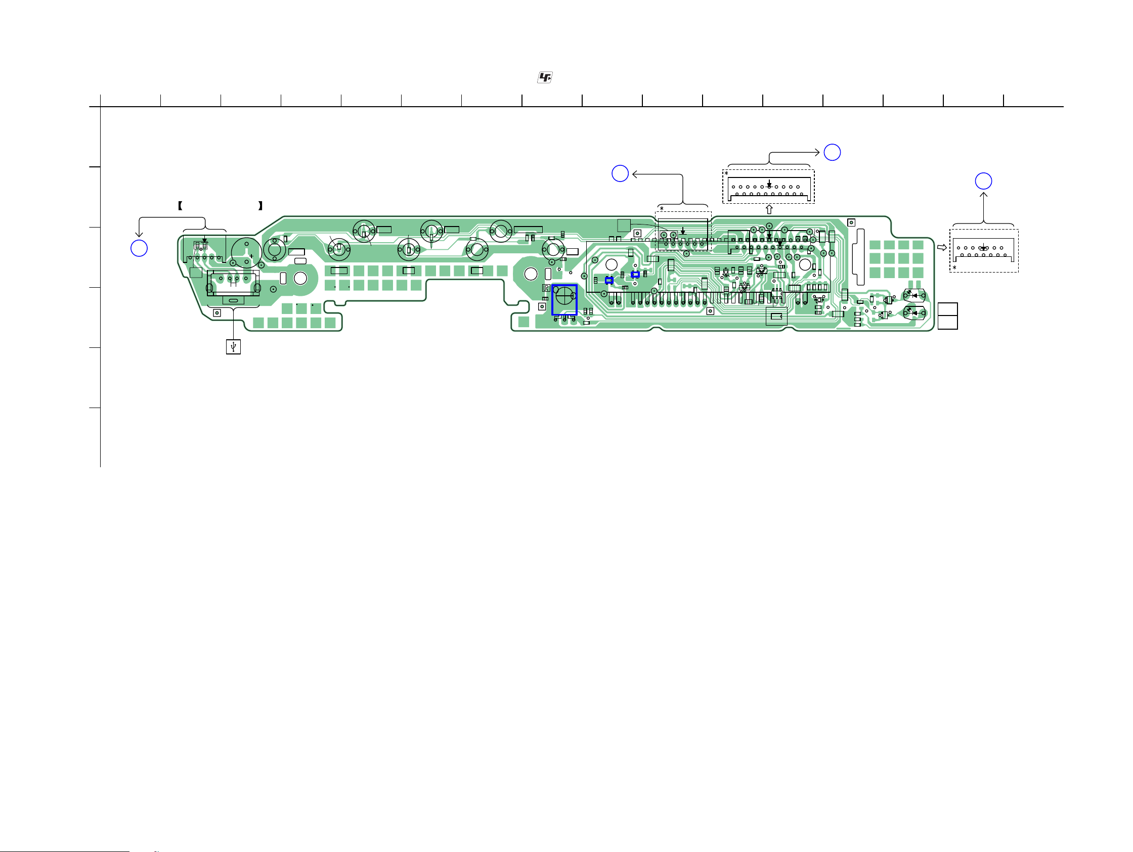
HBD-E2100/E3100/E3200/E4100/E6100
Ver. 1.5
6-19. PRINTED WIRING BOARD - PANEL Board - • See page 36 for Circuit Boards Location. • : Uses unleaded solder.
1
A
B
C
B
MB1002
BOARD
CN402
(Page 43)
D
2 3 4 5 6 7 8 9 10 11 12 13 14 15 16
MB1002
BOARD
CN805
(Page 43)
C
CN02
115
214
EXCEPT SP, RU
11
PANEL BOARD
CN51
15
C54
C53
JL53
CN52
C51
14
567
JL54
CL51
R07
VOL +
S07
R06
S06
VOL –
R08
S08
S02
MB1002
BOARD
D
CL03
R11
R17
JR05
JR
R12
D01
JR04
JR
CL05
R18
JR03
CN803
(Page 43)
CL07
JR11
JR
R26
JR
R29
R30
R24
R28
BE
Q02
1-887-134-
Q03
BE
D05
D06
(11)
KARAOKE
BOARD
CN71
(Page 58)
S03S04
FUNCTION
R01
R04
.>
R03
S01
N
R02
x
C01
CL15
R05
C21
C02
S05
Z
CL12
IC01
C26
OVS
R09
C04
CL17
CL16
G
CL71
CL72
JR
JR07
C05
C23
1
1
C22
IC03
C03
2528 1215
VACUUM FLUORESCENT DISPLAY
SP, RU
CN03
16
JR09
IC02
JR
C06
ND01
CL18
R21
CL73
JR
JR08
R13
21 1
20 2
21
20
C24
D04
JR10
R20
JR
C16
CN01
R19
C15
C14
CL13
15
14
C13
D03
R22
D02
CL11
C12
CN01SP, RU
CL10
CL09
C10
CL08
Q01
B1C2 E1
B2E2 C1
JR
JR06
CL06
CN02
CL04
JR02
CL14
1
CL01
2
CL02
R10
R15
R16
JR
R14
C11
E
F
HBD-E2100/E3100/E4100/E6100
5656
Page 57
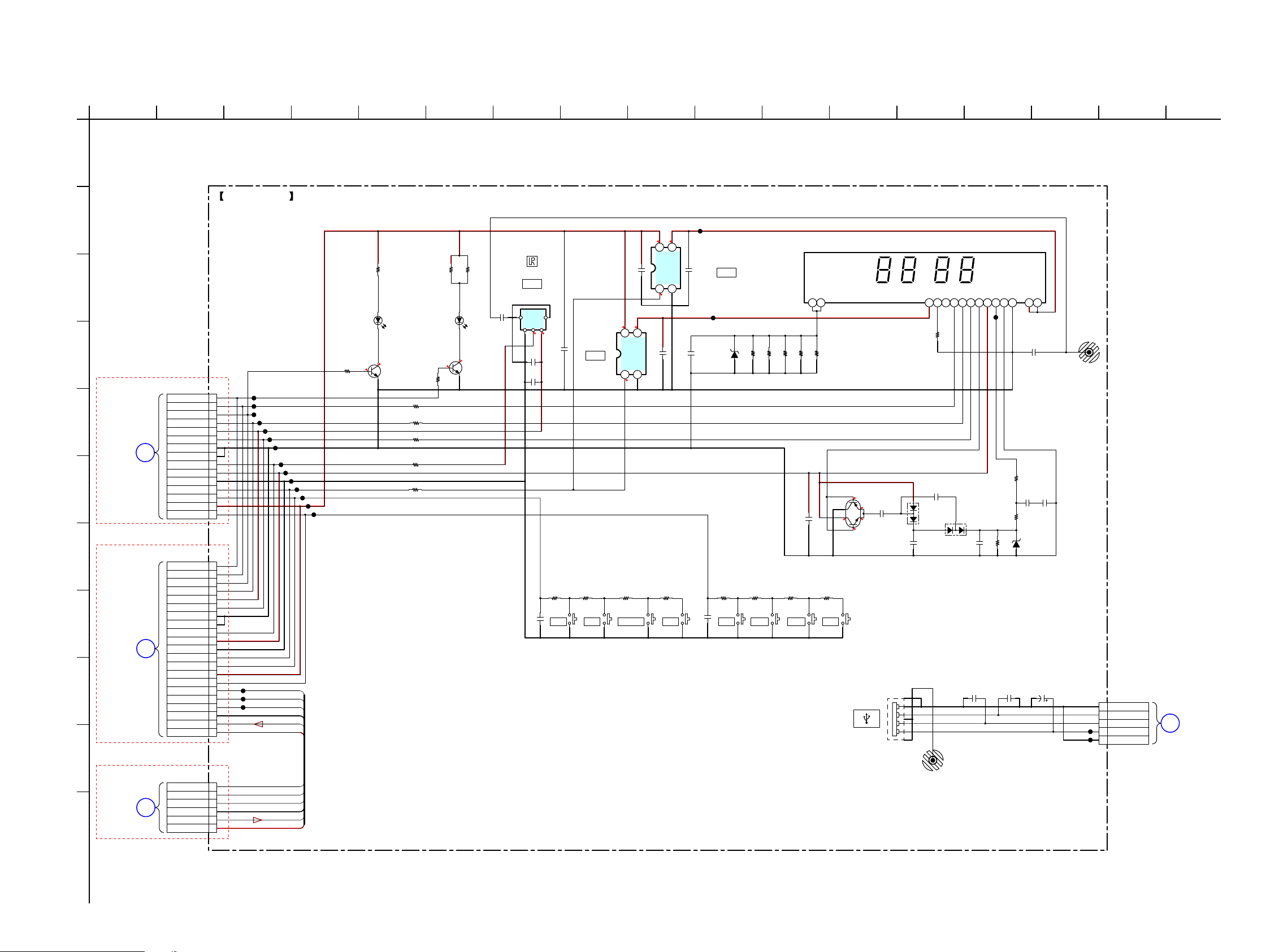
6-20. SCHEMATIC DIAGRAM - PANEL Board -
HBD-E2100/E3100/E3200/E4100/E6100
Ver. 1.5
A
B
C
D
E
F
G
H
I
J
K
1
MB1002
BOARD
(6/6)
CN805
(Page 50)
MB1002
BOARD
(6/6)
CN803
(Page 50)
KARAOKE
BOARD
CN71
(Page 58)
D
E
F
2 3 4 5 6 7 8 9 10 11 12 13 14 15 16 17
PANEL BOARD
CL16
EXCEPT SP, RU
BT_LED
FL_DOUT
WHITE_LED
FL_CLK
UNSW3.3V
FL_CS
FL_GND
FL_GND
SIRCS_IN
PANEL12V
GND
PCONT_FL
KEY2
PANEL5.5V
KEY1
SP, RU
BT_LED
FL_DOUT
WHITE_LED
FL_CLK
UNSW3.3V
FL_CS
FL_GND
FL_GND
SIRCS_IN
PANEL12V
GND
PCONT_FL
KEY2
PANEL5.5V
KEY1
MIC_DET
AGND
MIC_SIG
SP, RU
SDA
MIC_DET
SCL
AGND
MIC_SIG
A5V
3.35.5
3
4
Vin
R26
220
Q02
R12
R11
R10
D05
1L0353B14E0MKT01
BT LED
R28
10k
220
220
220
47R09
1kR22
D06
1L0353W34A0MKT01
WHITE LED
R24
10k
CN02
15P
1
2
3
4
5
6
7
8
9
10
11
12
13
14
15
CN01
21P
1
2
3
4
5
6
7
8
9
10
11
12
13
14
15
16
SDA
17
18
SCL
19
20
21
A5V
CN03
6P
1
2
3
4
5
6
CL71
CL72
CL73
CL03
CL01
CL14
CL02
CL05
CL04
CL06
CL07
MIC_DET
MIC_SIG
MIC_DET
MIC_SIG
CL08
AGND
AGND
CL09
CL10
CL11
CL12
CL13
SDA
SCL
A5V
SDA
SCL
A5V
0
0
LSCR523UBFS8TL
LED DRIVER
R29
220
0
R30
220
0
Q03
LSCR523UBFS8TL
LED DRIVER
REMOTE CONTROL
SIGNAL RECEIVER
C26
470p
IC01
GP1UE27XK0VF
IC01
GND
OUT
3.3 3.3
C03
0.01
C04
4.7
C01
0.1
C22
1
VS
C05
1
R01
100
S01
N
IC02
MM3411A33URE
IC02
+3.3V REG
R02
1k
S02
x
3.35.5
4
Vin
CE2GND
1
3.3
R03
2.2k
S03
FUNCTION
3
Vout
Vout
GND
1CE2
3.3
C06
C11
1
1
R04
2.2k
S04
.
MM3411Z41URE
C23
1
CL17
D01
UDZVTE-172.0B
C02
0.1
IC03
IC03
+3.3V REG
R05
100
S05
Z
R14
R15
100
100
R06
1k
S06
VOL –
F-
1
R1775R18
R16
75
100
6
C12
6
6
Q01
BC817DPN
1
6
C10
0.1
R07
2.2k
S07
VOL +
DISPLAY SW DRIVER
R08
2.2k
S08
>
12
ND01
VACUUM FLUORESCENT DISPLAY
OSC
VDD
1516171819202122232425 27282
R13
33k
C14 1
D02
BAV99-215
CN52
C13
1
4P
4
3
2
1
BAV99-215
CL51
DOUT
F+
LGND
PGND
VH
VIN
SW
STB
CLK
DIN
CL18
C21
470p
CL15
R21
10
C16
C24
0.22
0.22
R20
10
C15
D03
R19
1
C54
10p
D04
33k
DZ2J300M0L
C51
C53
220
10p
10V
JL53
JL54
CN51
5P
1GND
2DP
3DM
4 VBUS
5 SHIELD GND
A
MB1002
BOARD
(3/6)
CN402
(Page 47)
HBD-E2100/E3100/E4100/E6100
5757
Page 58
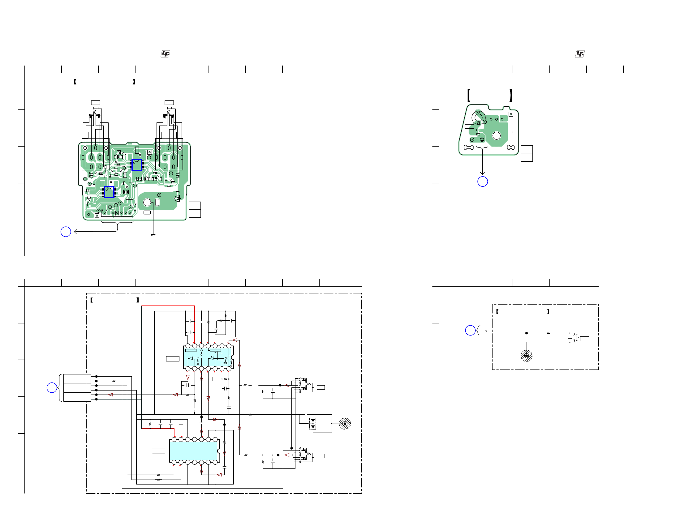
HBD-E2100/E3100/E3200/E4100/E6100
Ver. 1.5
6-21. PRINTED WIRING BOARD – KARAOKE Board (SP, RU) –
• See page 36 for Circuit Boards Location.
1
2 3 4 5 6 7 8
•
: Uses unleaded solder.
KARAOKE BOARD
G
(SP, RU)
J71 J72
MIC 1 MIC 2
C95
C94
R76
R75
C85
CL84
R82
C74
IC72
173
CN71
R72
CL72
C86
C82
CL73
R80
R81
JW52
JR
C87
C88
JW53
CL74
JR
CL75
C84
CL83
CL77
R71
C73
C93
R85
R84
CL71
R86
CL80
IC71
C78
C79
C81
C80
R79
C77
R78
CL76
C89
CL81
R88
1-887-377-
(CHASSIS)
R77
CL79
R73
C75
R74
C76
R87
C71
D71
11
(11)
A
B
C
D
PANEL
BOARD
E
CN03
(Page 56)
6-23. PRINTED WIRING BOARD – POWER KEY Board –
A
• See page 36 for Circuit Boards Location.
1
2 3 4 56
POWER KEY
•
: Uses unleaded solder.
BOARD
S41
CL42
CL41
&/1
TP41
C41
R41
B
11
1-887-135-
(11)
C
A
MB1002
BOARD
D
E
CN804
(Page 43)
6-22. SCHEMATIC DIAGRAM - KARAOKE Board (SP, RU) - 6-24. SCHEMATIC DIAGRAM - POWER KEY Board -
A
B
C
D
E
1
PANEL
BOARD
CN03
(Page 57)
F
2 3 4 5 6 7 89
KARAOKE BOARD
(SP, RU)
OUT1
IN1
R78
1M
27k
R77
C77
10k
C78
R79
4.7
C85
1
NC
NC
1
141312111098
1234567
C74
R72
R76
47k
C94
270p
R75
1k
C95
2.2
CL83
R82
0
NC
NC
12
C93
2.2
0.22
1k
R86
0
C76
R74
0.22
1k
CL77
C73
R71
1000p
100k
CL80
CL79
C75
R73
1000p
100k
C71
1000p
J71
MIC 1
D71
BAV99-215
J72
MIC 2
CL81
MIC_DET
AGND
MIC_SIG
C80
10
10
C81
C79
0.1
2.55 0.9 2.5 2.5
Bias Detector
IC71
NJM2783V (TE2)
IC71
C89
0.1
IC72
NJU72341V (TE2)
IC72
ELECTRICAL
VOLUME
100R84
100R85
MIC AMP
C88
C87
10
10
5 2.5 2.5
891011
VREF
SDA
SCL V+
7
3.3 3.3 2.5
2.5 2.5 2.5 2.5 2.5 2.5 2.5
C82
1000p
R80
R81
15k
8.2k
C84
0.1
CL84
C86
2.2
121314
GND
OUT2
IN2
MUTE
3
56
4
CN71
7P
SDA
SCL
A5V
CL71
1
CL72
CL73
CL74
CL75
CL76
100R87
R88
470
SCL
SDA
3
4
5
6
7
A
B
1
MB1002
BOARD
(6/6)
CN804
(Page 50)
C
2 34
POWER KEY BOARD
TP41
CL42
CL41
R41
100
C41
0.1
"/1
S41
HBD-E2100/E3100/E4100/E6100
5858
Page 59
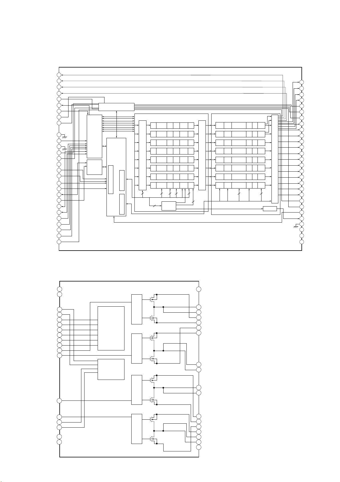
• IC Block Diagrams
IC3001 TAS5538DGGR (AMP BOARD (1/3))
1PWM_HPM_L
2PWM_HPP_L
3PWM_HPM_R
4PWM_HPP_R
5AVSS
6PLL_FLTM
7PLL_FLTP
8VR_ANA
9AVD D
10ASEL_VACS2
11MCLK
12OSC_RES
13DVSS2_CORE
14DVDD2_CORE
15VA CS_ 1
16XRESET
17XHP_SEL
18XPDN
19XMUTE
20SDA
21SCL
22LRCK
23SCLK
24SDIN1
25SDIN2
26SDIN3
27SDIN4
28VR_DIG
Serial
Control
Power Supply
Clock, PLL, and Serial Data I/F
Device
Control
2
I
C
System Control
I/F
PWM ControlDAP Control
HBD-E2100/E3100/E3200/E4100/E6100
Digital Audio Processor PWM Section
Soft
Soft
Tone
Soft
Tone
Soft
Tone
Soft
Tone
Soft
Tone
Soft
Tone
Soft
Tone
Soft
Tone
Volume
Control
Loud
DRC
Vol
Comp
Soft
Loud
DRC
Vol
Comp
Soft
Loud
DRC
Vol
Comp
Soft
Loud
DRC
Vol
Comp
Soft
Loud
DRC
Vol
Comp
Soft
Loud
DRC
Vol
Comp
Soft
Loud
DRC
Vol
Comp
Soft
Loud
DRC
Vol
Comp
2
7
0
Biquads
Det
7
0
Biquads
Det
7
0
Biquads
Det
8.8 Crossbar Mixer
7
0
Biquads
Det
7
0
Biquads
Det
7
0
Biquads
Det
7
0
Biquads
Det
7
0
Biquads
Det
88842
9
Block
Block
Block
8.2 Crossbar Mixer
Block
Block
Block
Block
Block
Ver. 1.5
56 PWM_P_6
55 PWM_M_6
54 PWM_P_5
53 PWM_M_5
52 VR_PWM
51 AVSS_PWM
50 AVDD_PWM
De
DC
Interpolate
Emph
De
DC
Interpolate
Emph
De
DC
Interpolate
Emph
De
DC
Interpolate
Emph
De
DC
Interpolate
Emph
De
DC
Interpolate
Emph
De
DC
Interpolate
Emph
De
DC
Interpolate
Emph
NS PWM
SRC
NS PWM
SRC
NS PWM
SRC
NS PWM
SRC
NS PWM
SRC
NS PWM
SRC
NS PWM
SRC
NS PWM
SRC
8
Output Control
8
PSVC
49 PWM_P_8
48 PWM_M_8
47 PWM_P_7
46 PWM_M_7
45 PWM_P_4
44 PWM_M_4
43 PWM_P_3
42 PWM_M_3
41 PWM_P_1
40 PWM_M_2
39 PWM_P_1
38 PWM_M_1
37 VALID
36 DVSS1_CORE
35 DVDD1_CORE
34 XBKND_ERR
33 PSVC
32 TEST
31 LRCLKO
30 SCLKO
29 SDOUT
IC3102 ST
A516BF13TR-A (AMP BOARD (3/3))
IC3302 STA516BF13TR-A (AMP BOARD (2/3))
19GND_CLEAN
20GND_REG
21VDD
22VDD
23VL
24CONFIG
25xPWRDN
26xTRISTATE
PROTECTIONS
&
LOGIC
27xFAULT
28TH_WARN
29IN1A
30IN1B
REGULATORS
31IN2A
32IN2B
33VSS
34VSS
35VCC_SIGN
36VCC_SIGN
M3
M2
M5
M4
M17
M15
M16
M14
18 NC
17 OUT1A
16 OUT1A
15 VCC1A
14 GND1A
13 GND1B
12 VCC1B
11 OUT1B
10 OUT1B
9OUT2A
8OUT2A
7 VCC2A
6 GND2A
5 GND2B
4 VCC2B
3OUT2B
2OUT2B
1 GND_SUB
59
Page 60
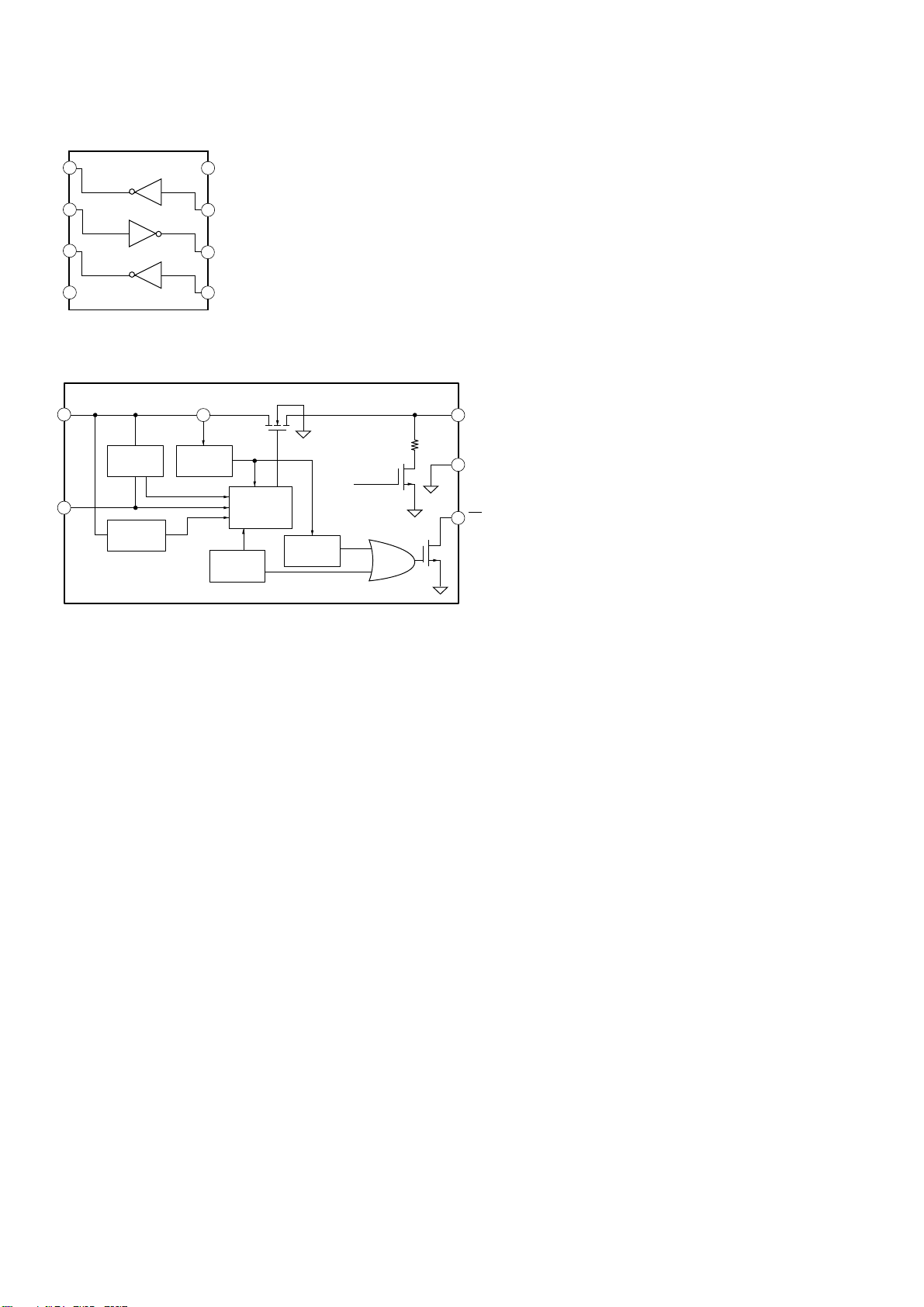
HBD-E2100/E3100/E3200/E4100/E6100
Ver. 1.5
IC403 TC7WHU04FK (MB1002 BOARD (3/6))
52Y
63A
71Y
8VCC
4GND
32A
23Y
11A
IC406 TPS2065CDBVR (MB1002 BOARD (3/6))
Current
Charge
Pump
UVLO
Sense
CS
Current
Limit
OTSD
Thermal
Sense
Driver
9-ms
Deglitch
5IN
4EN
(Disabled+
UVLO)
1OUT
2GND
FLT
3
3
60
Page 61
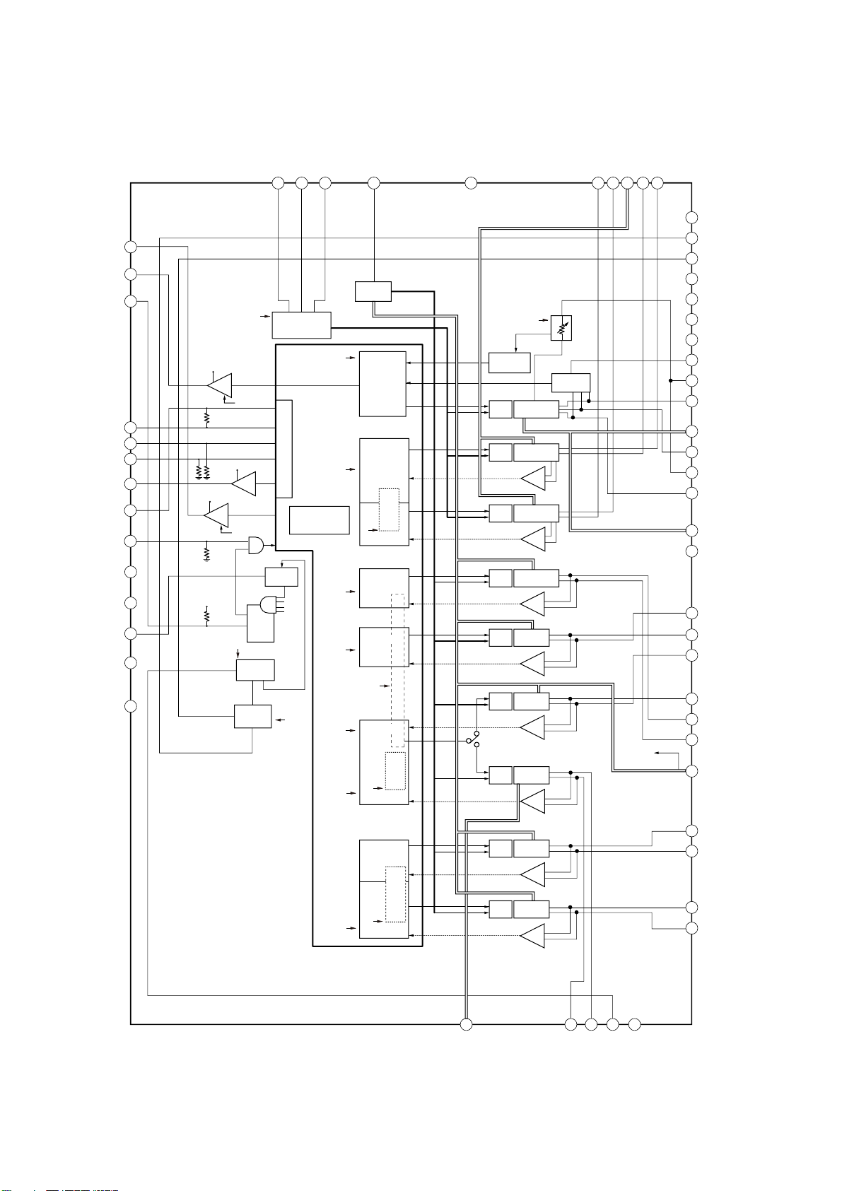
IC601 TPIC2060ADFDRG4 (MB1002 BOARD (4/6))
HBD-E2100/E3100/E3200/E4100/E6100
Ver. 1.5
CP39CP28CP1
10
11GPOUT
12XFG
13RDY
SIOV
Power
monitor
int 3.3V
Regulator
P5V
SIOV
P12V
LIN9V_DIS
Charge
pump
SPI I/F
thermometer
SPM_ENA
Digital core
SLD_ENA
On chip
TLT_ENA
FCS_ENA
TRK_ENA
XSLEEP
SIOV
XSLEEP
SIOV
SIOV
200k
200k200k
33k
GPOUTENA
P5V
5V Analog
LDO
control
14SSZ
15SCLK
16SIMO
17SOMI
18SIOV
19XRSTIN
20NC
21NC
22CV3P3
23AGND
24NC
7
int 10V
Regulator
19V
SPM Logic
DAC PWM
DAC PWM
SLD_E_ENA
DAC PWM
DAC PWM
ACTTEMPTH>0
DAC PWM
C10V
det
SLED END
ACTTEMP
PGND_2
6
SPM_RCOM
SPM
Current limit
pre
-driver
pre
-driver
I-F/B
pre
-driver
I-F/B
pre
-driver
F/B
pre
-driver
F/B
pre
-driver
F/B
pwr FET
pwr FET
pwr FET
pwr FET
pwr FET
pwr FET
BEMF
detector
SLED2_N4SLED2_P3P12V_SLD2SLED1_N1SLED1_P
5
analog
56 NC
55 LIN FB
54 LIN 9VG
53 TEST
52 NC
51 AGND
50 NC
49 MCOM
48 PGND_SPM2
47 W
46 P12V_SPM2
45 V
44 PGND_SPM1
43 U
42 P12V_SPM1
41 PGND_1
40 FCS_N
39 FCS_P
38 TRK_N
37 TRK_P
36 TLT_P
35 TLT_N
LOAD_ENA
TRAY_E_ENA
DAC PWM
det
TRAY xxx
pre
-driver
F/B
pre
-driver
pwr FET
pwr FET
34 P5V
33 STP1_P
32 STP1_N
det
STP_ENA
STEP END
STEP_E_ENA
F/B
pre
-driver
F/B
pwr FET
31 STP2_P
30 STP2_N
TPIC2060A
27
25
P5V12L
26
LOAD_N
28
LOAD_P
CA5V
29
NC
61
Page 62
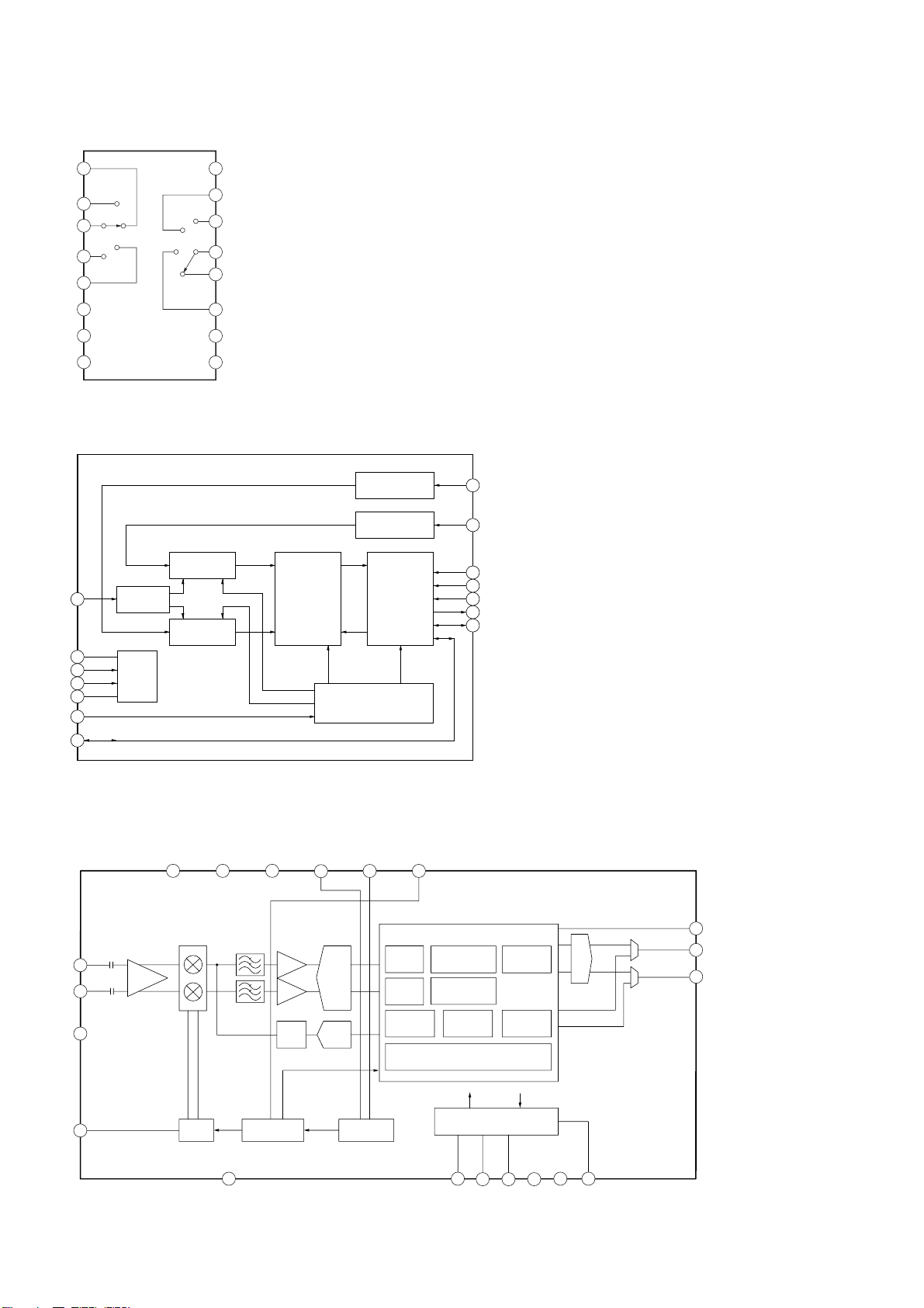
HBD-E2100/E3100/E3200/E4100/E6100
Ver. 1.5
IC703 SN74LV4052APWR (MB1002 BOARD (5/6))
16
1
2Y0
2Y2
2
3
2-COM
2Y3
4
5
2Y1
6
INH
7
GND
GND
8
IC704 PCM1808PWR (MB1002 BOARD (5/6))
VCC
15
1Y2
1Y1
14
1-COM
13
12
1Y0
11
1Y3
A
10
9
B
VREF 1
AGND
VCC
VDD
DGND
SCKI
LRCK
ANTIALIAS
LOW-PASS FILTER
ANTIALIAS
LOW-PASS FILTER
DELTA-SIGMA
MODULATOR
REFERENCE
DELTA-SIGMA
MODULATOR
2
3
4
5
6
7
POWER
SUPPLY
u1/64
DECIMATION
FILTER
WITH
HIGH-PASS
FILTER
CLOCK & TIMING CONTROL
SERIAL
INTERFACE
&
MODE/FORMAT
CONTROL
VINR
14
VINL
13
FMT12
MD111
MD010
DOUT9
BCK8
IC706 RN5B701-0001 (MB1002 BOARD (5/6)) (except AEP and UK models)
FRF1
FRF2
GNDRF
AGC
AMP
AGC
AMP
AGC
DET
X2
17
VDDRF
20
1
FM LNA
2
3
GND
19
VDD
18
Filter
ADC
ADC
X1
16
15
Digital Signal Processing
Digital
MixerFMDemodulator
Digital
AGC
Image
Control
CP1
RSSI
Calculation
Station
Detector
Digital Filters
Stereo
Decoder
IIS
Generator
IISD
LRCK
BCLK
DAC
LOUT
ROUT
IISD14
LRCK/LOUT
13
BCLK/ROUT
12
62
CP2
Serial Interface/Registers
6
7CK8
LA
IIC/RDSI
11
10
9
GND
DA
VDD
5
GNDRF
Clock
Generator
XOSC
4
LOSC
Page 63
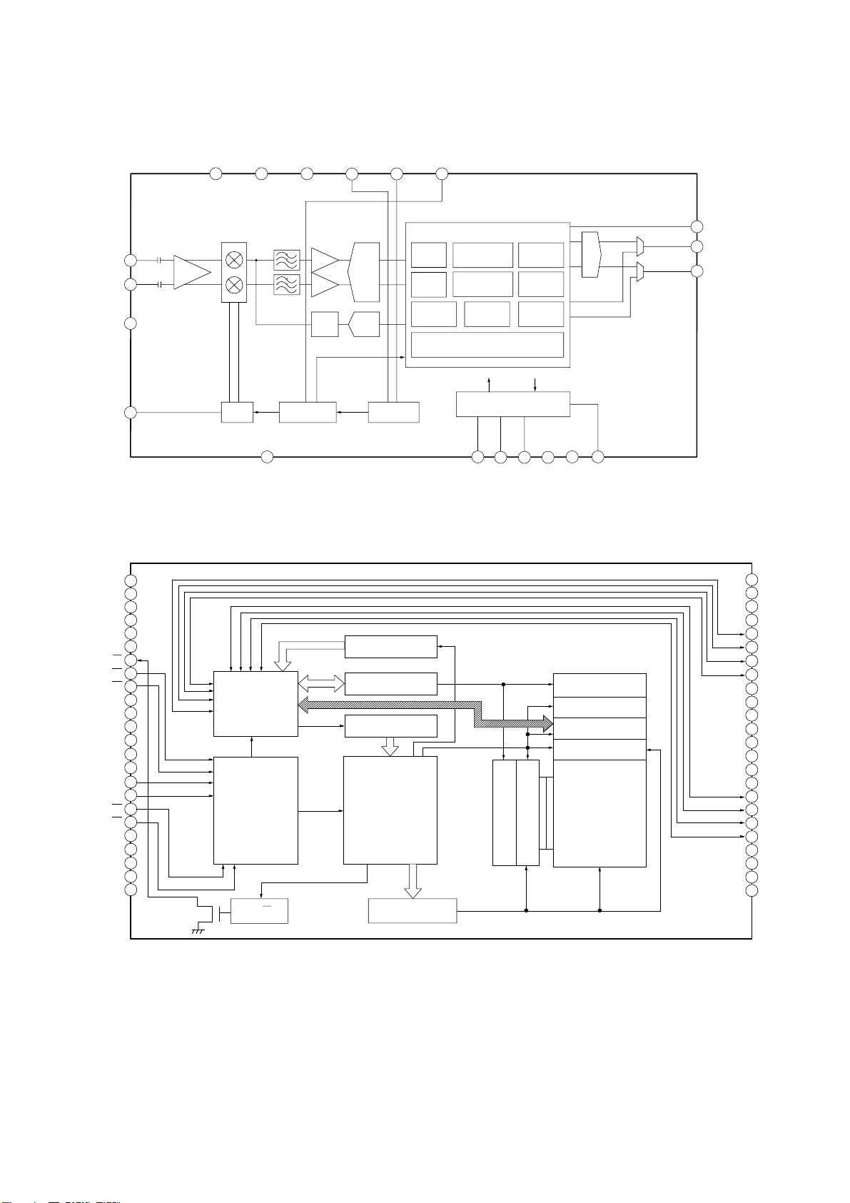
HBD-E2100/E3100/E3200/E4100/E6100
IC706 RN5B701-0002 (MB1002 BOARD (5/6)) (AEP and UK models)
Ver. 1.5
FRF1
FRF2
GNDRF
CP2
AGC
AMP
AGC
AMP
AGC
DET
X2
17
Filter
GNDRF
VDD
18
Clock
Generator
VDDRF
20
1
FM LNA
2
3
4
GND
19
LOSC
5
X1
16
ADC
ADC
XOSC
IC1001 H27U2G8F2CTR-BCR (MB1002 BOARD (1/6))
CP1
15
Digital Signal Processing
Digital
MixerFMDemodulator
Digital
AGC
Image
Control
RSSI
Calculation
Detector
Digital Filters
Serial Interface/Registers
6
Station
IIC/RDSI
7CK8
LA
Stereo
Decoder
RDS
Decoder
IIS
Generator
9
VDD
10
IISD
LRCK
BCLK
GND
DAC
11
LOUT
ROUT
DA
IISD14
LRCK/LOUT
13
BCLK/ROUT
12
1NC
2NC
3NC
4NC
5NC
6NC
7RY / BY
8RE
9CE
10NC
11NC
12VCC
13VSS
14NC
15NC
16CLE
17ALE
18WE
19WP
20NC
21NC
22NC
23NC
24NC
I/O
Control circuit
Logic control
RY/BY
Status register
Address register
Command register
Control circuit Memory cell array
Row address decoder
Row address buffer decoder
HV generator
Column buffer
Column decoder
Data register
Sense amp
48 NC
47 NC
46 NC
45 NC
44 IO8
43 IO7
42 IO6
41 IO5
40 NC
39 NC
38 NC
37 VCC
36 VSS
35 NC
34 NC
33 NC
32 IO4
31 IO3
30 IO2
29 IO1
28 NC
27 NC
26 NC
25 NC
63
Page 64

HBD-E2100/E3100/E3200/E4100/E6100
Ver. 1.5
• IC Pin Function Descriptions
MB1002 BOARD (1/6), (3/6), (4/6) IC101 CXD90019R-BA (BD DECODER)
Pin No. Pin Name I/O Description
P1 TRINB I Input of Tracking Signal (B)
P2 TRINA I Input of Tracking Signal (A)
P3 HAVC O Decoupling Pin for Reference Voltage of Main and Sub Beams
P4 AVDD33_1 - 3.3 V Power Pin
P5 INB I Input of Main Beam Signal (B)
P6 INA I Input of Main Beam Signal (A)
P7 IND I Input of Main Beam Signal (D)
P8 INC I Input of Main Beam Signal (C)
P9 ING I Input of Main Beam Signal (G)
P10 INH I Input of Main Beam Signal (H)
P11 INF I Input of Main Beam Signal (F)
P12 INE I Input of Main Beam Signal (E)
P13 V14 O Output of Voltage Reference (1.4 V)
P14 AUX1 I/O
P15 MPXOUT1 O
P16 MPXOUT2 O
P17 MPXOUT3 O
P18 RFIP I Differential Input of AC Coupling RF SUM Signal (Positive)
P19 RFIN I Differential Input of AC Coupling RF SUM Signal (Negative)
P20 RFIP2 I Differential Input of AC Coupling RF SUM Signal (Positive)
P21 RFIN2 I Differential Input of AC Coupling RF SUM Signal (Negative)
P22 AVDD12_2 - 1.2 V Power Pin
P23 AVDD33_3 - 3.3 V Power Pin
P24 FOO O Focus servo output. PDM output of focus servo compensator.
P25 TRO O Tracking servo output. PDM output of tracking servo compensator.
P26 TLO O Tilt servo output
P27 DVCC12_K_1 - 1.2V Digital Power
P28 FEOSCEN I/O
P29 FEGAINSW3 O Read gain switch 3.
P30 FECFREQ I/O
P31 FECMOD I/O
P32 FEGAINSW1 O Read gain switch 1.
P33 FEGAINSW2 O Read gain switch 2.
P34 FEFMO I/O
P35 FEFMO2 O Feed motor 2 control. DAC output.
P36 DVCC33_IO_1 - 3.3V Digital IO Power
P37 FEFMO3 I/O
P38 FEFMO4 I/O
P39 FETRAYPWM O Tray DAC / PWM control input. Controlled by uP.
P40 FEDMO O Disk motor control output. DAC output.
P41 FEFG I Motor Hall sensor input.
P42 DVCC12_K_2 - 1.2V Digital Power
Auxiliary Input
Alternative function: Signal Monitoring
Multiplexer Output 1 for Signal Monitoring. The pin is not allowed to pull-up in circuit layout.
Alternative function: Internal monitored signal output / General output.
Multiplexer Output 2 for Signal Monitoring. The pin is not allowed to pull-up in circuit layout.
Alternative function: Internal monitored signal output / General output.
Multiplexer Output 3 for Signal Monitoring. The pin is not allowed to pull-up in circuit layout.
Alternative function: Internal monitored signal output / General output.
High frequency modulation enable signal output, or LDD serial interface CLK or I2C SCL.
The pin is spike-free at power-on stage.
Frequency selection signal output, or LDD serial interface data or I2C SDA.
The pin is spike-free at power-on stage.
High frequency modulation mode selection signal output, or LDD serial interface command
enable.
The pin is spike-free at power-on stage.
Feed motor 4 control. DAC output.
Alternative function: Auxiliary servo input
Feed motor 3 control. DAC output.
Alternative function: Auxiliary servo input
Feed motor 4 control. DAC output.
Alternative function: Auxiliary servo input
64
Page 65

HBD-E2100/E3100/E3200/E4100/E6100
Pin No. Pin Name I/O Description
P43 FEGIO0 I/O
P44 FEGIO1 I/O PC RS232 serial receive data. The pin is spike-free at power-on stage.
P45 FEGIO5 O General IO
P46 DVCC33_IO_2 - 3.3V Digital IO Power
P47 FEGIO7 I/O
P48 FEGIO6 O
P49 FEGIO4 O
P50 FEGIO9 I/O
P51 FEGIO10 I/O PC RS232 serial receive data. The pin is spike-free at power-on stage.
P52 FEGIO11 I/O PC RS232 serial transmit data. The pin is spike-free at power-on stage.
P53 FETRAYIN_ I A logical Low indicates the Tray is IN
P54 FEGIO3 I/O
P55 USB_DM_P1 I/O USB port1 differential serial data bus (minus)
P56 USB_DP_P1 I/O USB port1 differential serial data bus (plus)
P57 USB_VRT_P1 - USB port1 reference resistor
P58 AVDD33_USB_P1 - 3.3V Analog power for USB port1
P59 EFPWRQ - 2.5 V power for E-fuse programming
P60 DVCC12_K_3 - 1.2V Digital Power
P61 DVCC33_IO_3 - 3.3V Digital IO Power
P62 SCL I USB over current Protection indication
P63 SDA I USB PCONT
P64 SPDIF_IN1 I HDMI ARC SPDIF input
P65 NFD0 I/O NAND Flash Data input/output bit0
P66 NFD1 I/O NAND Flash Data input/output bit1
P67 NFD2 I/O NAND Flash Data input/output bit2
P68 NFD3 I/O NAND Flash Data input/output bit3
P69 NFD4 I/O NAND Flash Data input/output bit4
P70 NFD5 I/O NAND Flash Data input/output bit5
P71 NFD6 I/O NAND Flash Data input/output bit6
P72 DVCC33_IO_4 - 3.3V Digital IO Power
P73 NFD7 I/O NAND Flash Data input/output bit7
P74 NFRBN I/O NAND Flash ready / busy
P75 NFREN I/O NAND Flash read enable
P76 NFCEN I/O NAND Flash chip enable
P77 NFCLE I/O NAND Flash command latch enable
P78 NFALE I/O NAND Flash address latch enable
P79 NFWEN I/O NAND Flash write enable
P80 DVCC12_K_4 - 1.2V Digital Power
P81 DDRVCCK_1 - 1.2V Digital Power
P82 RDQ4 I/O Memory data bit 4
P83 RDQ6 I/O Memory data bit 6
P84 RDQ2 I/O Memory data bit 2
P85 DDRVCCIO_1 - 1.5V Digital IO Power
P86 RDQ0 I/O Memory data bit 0
P87 RDQ11 I/O Memory data bit 11
P88 RDQ9 I/O Memory data bit 9
P89 RDQ13 I/O Memory data bit 13
P90 RDQ15 I/O Memory data bit 15
LDD serial interface data. The pin is spike-free at power-on stage.
The pin is not allowed to pull-up in circuit layout.
General IO
General IO. The pin is spike-free at power-on stage. The pin is not allowed to pull-up in
circuit layout.
Read gain switch 6. The pin is not allowed to pull-up in circuit layout.
General IO
Read gain switch 4
General IO
General IO. The pin is spike-free at power-on stage.
General IO
LED Control Output. Initial 0 Output. The pin is spike-free at power-on stage.
General IO
Ver. 1.5
65
Page 66

HBD-E2100/E3100/E3200/E4100/E6100
Ver. 1.5
Pin No. Pin Name I/O Description
P91 RDQM1 O Memory data mask bit 1
P92 DDRVCCK_2 - 1.2V Digital Power
P93 DDRVREF I Memory VREF
P94 RDQS0 I/O Memory positive data strobe bit 0
P95 RDQS0_ I/O Memory negative data strobe bit 0
P96 DDRVCCIO_2 - 1.5V Digital IO power
P97 RCLK0_ O Memory clock 0 negative
P98 RCLK0 O Memory clock 0 positive
P99 RDQM0 O Memory data mask bit 0
P100 RDQS1 I/O Memory positive data strobe bit 1
P101 RDQS1_ I/O Memory negative data strobe bit 1
P102 DDRVCCIO_3 - 1.5V Digital IO power
P103 RDQ12 I/O Memory data bit 12
P104 RDQ14 I/O Memory data bit 14
P105 RDQ10 I/O Memory data bit 10
P106 RDQ8 I/O Memory data bit 8
P107 RDQ1 I/O Memory data bit 1
P108 DDRVCCIO_4 - 1.5V Digital IO Power
P109 RDQ3 I/O Memory data bit 3
P110 RDQ7 I/O Memory data bit 7
P111 RDQ5 I/O Memory data bit 5
P112 DDRVCCK_3 - 1.2V Digital Power
P113 AVDD33_MEMPLL - 3.3 V Analog Power for MEMPLL
P114 TP_MEMPLL - Test Pin
P115 TN_MEMPLL - Test Pin
P116 RCKE O Memory clock enable
P117 RA10 O Memory address bit 10
P118 RBA1 O Memory bank address bit 1
P119 RA4 O Memory address bit 4
P120 RA1 O Memory address bit 1
P121 RA6 O Memory address bit 6
P122 RA8 O Memory address bit 8
P123 DDRVCCIO_5 - 1.5V Digital IO Power
P124 RA11 O Memory address bit 11
P125 RA12 O Memory address bit 12
P126 RRAS_ O Memory row address strobe
P127 RCAS_ O Memory column address strobe
P128 RCS_ O Memory chip select
P129 DDRVCCIO_6 - 1.5V Digital IO Power
P130 RWE_ O Memory write enable
P131 RA0 O Memory address bit 0
P132 RA13 O Memory address bit 13
P133 RA9 O Memory address bit 9
P134 RRESET O Memory reset
P135 RA7 O Memory address bit 7
P136 RA2 O Memory address bit 2
P137 RA5 O Memory address bit 5
P138 RA3 O Memory address bit 3
P139 RBA2 O Memory bank address bit 2
P140 RBA0 O RBA0
P141 RODT O Memory on die termination enable
P142 RCSX_ O Memory chip select
P143 DDRVCCIO_7 - 1.5V Digital IO Power
66
Page 67

HBD-E2100/E3100/E3200/E4100/E6100
Pin No. Pin Name I/O Description
P144 RDQ20 I/O Memory data bit 20
P145 RDQ22 I/O Memory data bit 22
P146 RDQ18 I/O Memory data bit 18
P147 DDRVCCIO_8 - 1.5V Digital IO power
P148 RDQ16 I/O Memory data bit 16
P149 RDQ27 I/O Memory data bit 27
P150 RDQ25 I/O Memory data bit 25
P151 RDQ29 I/O Memory data bit 29
P152 RDQ31 I/O Memory data bit 31
P153 RDQM3 O Memory data mask bit 3
P154 DDRVCCK_4 - 1.2V Digital Power
P155 DDRVREF I Memory VREF
P156 DDRVCCIO_9 - 1.5V Digital IO Power
P157 RDQS2 I/O Memory positive data strobe bit 2
P158 RDQS2_ I/O Memory negative data strobe bit 2
P159 RCLK1_ O Memory clock 1 negative
P160 RCLK1 O Memory clock 1 positive
P161 DDRVCCIO_A - 1.5V Digital IO Power
P162 RDQM2 O Memory data mask bit 2
P163 RDQS3 I/O Memory positive data strobe bit 3
P164 RDQS3_ I/O Memory negative data strobe bit 3
P165 RDQ28 I/O Memory data bit 28
P166 RDQ30 I/O Memory data bit 30
P167 RDQ26 I/O Memory data bit 26
P168 RDQ24 I/O Memory data bit 24
P169 RDQ17 I/O Memory data bit 17
P170 DDRVCCIO_B - 1.5V Digital IO power
P171 RDQ19 I/O Memory data bit 19
P172 RDQ23 I/O Memory data bit 23
P173 RDQ21 I/O Memory data bit 21
P174 DDRVCCK_5 - 1.2V Digital Power
P175 DVCC12_K_5 - 1.2V Digital Power
P176 AVDD33_LDO - Line driver 3.3V analog power
P177 AVDD12_LDO - 1.2 V standby power
P178 OPWRSB I/O Power Control
P179 GPIO8 I/O ICE1_TDO
P180 GPIO7 I/O ICE1_TCK
P181 GPIO6 I/O ICE1_TMS
P182 GPIO5 I/O ICE1_TDI
P183 GPIO4 - Not used
P184 DVCC33_IO_STB_1 - 3.3V Digital IO Power for Stand-By Module
P185 GPIO3 I/O WOL_INT
P186 GPIO2 I/O START_BIT
P187 GPIO1 I/O XIF_CS
P188 GPIO0 I IF_SDI
P189 VCLK - IF_SCK
P190 VSTB I SYS_REQ
P191 VDATA O IF_SDO
P192 IR I SIRCS
P193 RESET_ I Power on reset
P194 UATXD I/O
Reserved for debug-only Uart pins.
(1) 1st RS232 TX
(2) T8032 RS232 TX
Ver. 1.5
67
Page 68

HBD-E2100/E3100/E3200/E4100/E6100
Ver. 1.5
Pin No. Pin Name I/O Description
P195 UARXD I/O
P196 AMUTE I UPG_STATUS
P197 HTPLG I/O HDMI Hot Plug
P198 DVCC33_IO_STB_2 - 3.3V Digital IO Power for Stand-By Module
P199 HDMISD I/O HDMI I2C data
P200 HDMISCK I/O HDMI I2C clock
P201 CEC I/O HDMI CEC
P202 LED1 I JIG_MODE0
P203 LED0 I JIG_MODE1
P204 USB_DM_P2 I/O USB port2 differential serial data bus (minus)
P205 USB_DP_P2 I/O USB port2 differential serial data bus (plus)
P206 USB_VRT_P2 - USB port2 reference resistor
P207 AVDD33_USB_P2 - 3.3V Analog Power for USB port2
P208 AVSS33_BG - BG Analog Ground
P209 REXT O External reference resistor
P210 AVDD33_COM - PLL / BG 3.3 V Analog Power
P211 TXVN_1 I/O Ethernet RD -
P212 TXVP_1 I/O Ethernet RD +
P213 TXVN_0 I/O Ethernet TD -
P214 TXVP_0 I/O Ethernet TD +
P215 AVDD33_LD - 3.3 V power for standby
P216 DVCC12_K_6 - 1.2V Digital Power
P217 AVDD33_HDMI - 3.3 V Analog Power
P218 CLK_M O HDMI TX clock differential pair (M)
P219 CLK_P O HDMI TX clock differential pair (P)
P220 CH0_M O HDMI TX data 0 differential pair (M)
P221 CH0_P O HDMI TX data 0 differential pair (P)
P222 CH1_M O HDMI TX data 1 differential pair (M)
P223 CH1_P O HDMI TX data 1 differential pair (P)
P224 CH2_M O HDMI TX data 2 differential pair (M)
P225 CH2_P O HDMI TX data 2 differential pair (P)
P226 AVDD12_HDMI_C - 1.2 V Analog Power
P227 AVDD12_HDMI_D - 1.2 V Analog Power
P228 AVSS12_HDMI - 1.2V Analog Ground
P229 NS_XTALI - 3.3V power for standby
P230 NS_XTALO I 27MHz Crystal In
P231 AVDD33_PLLGP - 3.3 V Analog Power for PLL Group
P232 AVDD33_VDAC_BG - 3.3V Analog Power
P233 AVDD33_VDAC_X - 3.3V Analog Power
P234 VDACX_OUT O DAC output
P235 VMID_PWMDAC - PWMDAC internal LDO reference
P236 AVDD33_DAC - 3.3 V Analog Power
P237 AL0 I I2S Master Clock line
P238 AVSS33_DAC - Analog Ground
P239 AR0 I I2S Bit Clock line
P240 DVCC33_IO_7 - 3.3V Digital IO power
P241 SPDIF_IN0 I Microphone signal input
P242 AOLRCK I/O Audio output left-right clock
P243 AOSDATA0 I/O Audio output serial data 0
P244 AOSDATA1 I/O Audio output serial data 1
P245 AOSDATA2 I/O Audio output serial data 2
P246 AOSDATA3 I/O Audio output serial data 3
Reserved for debug-only Uart pins.
(1) 1st RS232 RX
(2) T8032 RS232 RX
68
Page 69

HBD-E2100/E3100/E3200/E4100/E6100
Pin No. Pin Name I/O Description
P247 SPDIF I/O SPDIF digital audio output
P248 DVCC12_K_7 - 1.2V Digital Power
P249 AVDD12_1 - 1.2 V Power Pin
P250 RSTI I Front-End Power on reset
P251 VDAC0 O Output of General DAC
P252 VWDC2O O Output Voltage 2 of Laser Diode Control in APC
P253 VWDC3O O Output Voltage 3 of Laser Diode Control in APC
P254 FVREF O Output of Voltage Reference
P255 FPDOCD I Laser Power Monitor Input for CD APC / Differential negative input
P256 FPDODVD I Laser Power Monitor Input for DVD APC / Differential positive input
P257 EPAD - DGND
Ver. 1.5
69
Page 70
HBD-E2100/E3100/E3200/E4100/E6100
Ver. 1.5
MB1002 BOARD (1/6) IC102, IC103 K4B2G1646Q-BCMA (SD-RAM)
Pin No. Pin Name I/O Description
A1 VDDQ - DQ Power Supply: 1.5V +/-0.075V
A2 DQU5 I/O Data Input/output: Bi-directional data bus.
A3 DQU7 I/O Data Input/output: Bi-directional data bus.
A4 NO_USE - Not used
A5 NO_USE - Not used
A6 NO_USE - Not used
A7 DQU4 I/O Data Input/output: Bi-directional data bus.
A8 VDDQ - DQ Power Supply: 1.5V +/-0.075V
A9 VSS - Ground
B1 VSSQ - DQ Ground
B2 VDD - Power Supply: 1.5V +/-0.075
B3 VSS - Ground
B4 NO_USE - Not used
B5 NO_USE - Not used
B6 NO_USE - Not used
Data Strobe: Output with read data, input with write data. Edge-aligned with read data, centered in write data. For the x16, DQSL: corresponds to the data on DQL0-DQL7; DQSU corre-
B7
B8 DQU6 I/O Data Input/output: Bi-directional data bus.
B9 VSSQ - DQ Ground
C1 VDDQ - DQ Power Supply: 1.5V +/-0.075V
C2 DQU3 I/O Data Input/output: Bi-directional data bus.
C3 DQU1 I/O Data Input/output: Bi-directional data bus.
C4 NO_USE - Not used
C5 NO_USE - Not used
C6 NO_USE - Not used
C7 DQSU I/O
C8 DQU2 I/O Data Input/output: Bi-directional data bus.
C9 VDDQ - DQ Power Supply: 1.5V +/-0.075V
D1 VSSQ - DQ Ground
D2 VDDQ - DQ Power Supply: 1.5V +/-0.075V
D3 DMU I
D4 NO_USE - Not used
D5 NO_USE - Not used
D6 NO_USE - Not used
D7 DQU0 I/O Data Input/output: Bi-directional data bus.
D8 VSSQ - DQ Ground
D9 VDD - Power Supply: 1.5V +/-0.075
E1 VSS - Ground
E2 VSSQ - DQ Ground
E3 DQL0 I/O Data Input/output: Bi-directional data bus.
E4 NO_USE - Not used
E5 NO_USE - Not used
E6 NO_USE - Not used
DQSU I/O
sponds to the data on DQU0-DQU7. The data strobe DQS, DQSL and DQSU are paired with
differential signals DQS, DQSL and DQSU, respectively, to provide differential pair signaling
to the system during reads and writes. DDR3 SDRAM supports differential data strobe only
and does not support single-ended.
Data Strobe: Output with read data, input with write data. Edge-aligned with read data, centered in write data. For the x16, DQSL: corresponds to the data on DQL0-DQL7; DQSU corresponds to the data on DQU0-DQU7. The data strobe DQS, DQSL and DQSU are paired with
differential signals DQS, DQSL and DQSU, respectively, to provide differential pair signaling
to the system during reads and writes. DDR3 SDRAM supports differential data strobe only
and does not support single-ended.
Input Data Mask: DM is an input mask signal for write data. Input data is masked when DM
is sampled HIGH coincident with that input data during a Write access. DM is sampled on
both edges of DQS. For x8 device, the function of DM or TDQS/ TDQS is enabled by Mode
Register A11 setting in MR1.
70
Page 71
HBD-E2100/E3100/E3200/E4100/E6100
Pin No. Pin Name I/O Description
Input Data Mask: DM is an input mask signal for write data. Input data is masked when DM
E7 DML I
E8 VSSQ - DQ Ground
E9 VDDQ - DQ Power Supply: 1.5V +/-0.075V
F1 VDDQ - DQ Power Supply: 1.5V +/-0.075V
F2 DQL2 I/O Data Input/output: Bi-directional data bus.
F3 DQSL I/O
F4 NO_USE - Not used
F5 NO_USE - Not used
F6 NO_USE - Not used
F7 DQL1 I/O Data Input/output: Bi-directional data bus.
F8 DQL3 I/O Data Input/output: Bi-directional data bus.
F9 VSSQ - DQ Ground
G1 VSSQ - DQ Ground
G2 DQL6 I/O Data Input/output: Bi-directional data bus.
G3
G4 NO_USE - Not used
G5 NO_USE - Not used
G6 NO_USE - Not used
G7 VDD - Power Supply: 1.5V +/-0.075
G8 VSS - Ground
G9 VSSQ - DQ Ground
H1 VREFDQ - Reference voltage for DQ
H2 VDDQ - DQ Power Supply: 1.5V +/-0.075V
H3 DQL4 I/O Data Input/output: Bi-directional data bus.
H4 NO_USE - Not used
H5 NO_USE - Not used
H6 NO_USE - Not used
H7 DQL7 I/O Data Input/output: Bi-directional data bus.
H8 DQL5 I/O Data Input/output: Bi-directional data bus.
H9 VDDQ - DQ Power Supply: 1.5V +/-0.075V
J1 NC - No Connect: No internal electrical connection is present.
J2 VSS - Ground
J3
J4 NO_USE - Not used
J5 NO_USE - Not used
J6 NO_USE - Not used
J7 CK I
J8 VSS - Ground
J9 NC - No Connect: No internal electrical connection is present.
K1 ODT I
K2 VDD - Power Supply: 1.5V +/-0.075
DQSL I/O
RAS I Command Input: RAS (along with CS) defi ne the command being entered.
is sampled HIGH coincident with that input data during a Write access. DM is sampled on
both edges of DQS. For x8 device, the function of DM or TDQS/ TDQS is enabled by Mode
Register A11 setting in MR1.
Data Strobe: Output with read data, input with write data. Edge-aligned with read data, centered in write data. For the x16, DQSL: corresponds to the data on DQL0-DQL7; DQSU corresponds to the data on DQU0-DQU7. The data strobe DQS, DQSL and DQSU are paired with
differential signals DQS, DQSL and DQSU, respectively, to provide differential pair signaling
to the system during reads and writes. DDR3 SDRAM supports differential data strobe only
and does not support single-ended.
Data Strobe: Output with read data, input with write data. Edge-aligned with read data, centered in write data. For the x16, DQSL: corresponds to the data on DQL0-DQL7; DQSU corresponds to the data on DQU0-DQU7. The data strobe DQS, DQSL and DQSU are paired with
differential signals DQS, DQSL and DQSU, respectively, to provide differential pair signaling
to the system during reads and writes. DDR3 SDRAM supports differential data strobe only
and does not support single-ended.
Clock: CK is differential clock input. All address and control input signals are sampled on the
crossing of the positive edge of CK. Output (read) data is referenced to the crossing of CK.
On Die Termination: ODT (registered HIGH) enables termination resistance internal to the
DDR3 SDRAM. When enabled, ODT is only applied to each DQ, DQS, DQS and DM/TDQS,
NU/TDQS (When TDQS is enabled via Mode Register A11=1 in MR1) signal for x8 confi gura-
tions. The ODT pin will be ignored if the Mode Register (MR1) is programmed to disable ODT.
Ver. 1.5
71
Page 72
HBD-E2100/E3100/E3200/E4100/E6100
Ver. 1.5
Pin No. Pin Name I/O Description
K3
K4 NO_USE - Not used
K5 NO_USE - Not used
K6 NO_USE - Not used
K7
K8 VDD - Power Supply: 1.5V +/-0.075
K9 CKE I
L1 NC - No Connect: No internal electrical connection is present.
CAS I Command Input: CAS (along with CS) defi ne the command being entered.
CK I
Clock: CK is differential clock input. All address and control input signals are sampled on the
crossing of the negative edge of CK. Output (read) data is referenced to the crossing of CK.
Clock Enable: CKE HIGH activates, and CKE LOW deactivates, internal clock signal and device input buffers and output drivers. Talking CKE LOW provides Precharge Power-Down and
Self Refresh operation (all banks idle), or Active Power-Down (Row Active in any bank). CKE
is asynchronous for self refresh exit. After V
initialization sequence, it must be maintained during all operations (including Self-Refresh).
CKE must be maintained high throughout read and write accesses. Input buffers, excluding
CK, CK, ODT and CKE are disabled during power-down. Input buffers, excluding CKE, are
disabled during Self-Refresh.
REFCA
has become stable during the power on and
L2
L3
L4 NO_USE - Not used
L5 NO_USE - Not used
L6 NO_USE - Not used
L7 A10 I
L8 ZQ - Reference Pin for ZQ calibration
L9 NC - No Connect: No internal electrical connection is present.
M1 VSS - Ground
M2 BA0 I
M3 BA2 I
M4 NO_USE - Not used
M5 NO_USE - Not used
M6 NO_USE - Not used
M7 NC - No Connect: No internal electrical connection is present.
M8 VREFCA - Reference voltage for CA
M9 VSS - Ground
N1 VDD - Power Supply: 1.5V +/-0.075
N2 A3 I
N3 A0 I
N4 NO_USE - Not used
N5 NO_USE - Not used
N6 NO_USE - Not used
N7 A12 I
CS I
WE I Command Input: WE (along with CS) defi ne the command being entered.
Chip Select: All commands are masked when CS is registered HIGH. CS provides for external
Rank selection on system with multiple Ranks. CS is considered part of the command code.
Address inputs: Provided the row address for active commands and the column address for
Read/Write commands to select one location out of the memory array in the respective bank.
The address inputs also provide the op-code during Mode Register Set commands.
Autoprecharge: A10 is sampled during Read/Write commands to determine whether Autoprecharge should be performed to the accessed bank after the Read/Write operation. (HIGH:
Autoprecharge; LOW: No Autoprecharge)
A10 is sampled during a Precharge command to determine the Percharge applies to one bank
(A10 LOW) or all banks (A10 HIGH). If only one bank is to be precharged, the bank is selected
by bank adresses.
Bank Address Inputs: BA0 defi ne to which bank an Active, Read, Write or Precharge com-
mand is being applied. Bank address also determines if the mode register or extended mode
register is to be accessed during a MRS cycle.
Bank Address Inputs: BA2 defi ne to which bank an Active, Read, Write or Precharge com-
mand is being applied. Bank address also determines if the mode register or extended mode
register is to be accessed during a MRS cycle.
Address inputs: Provided the row address for active commands and the column address for
Read/Write commands to select one location out of the memory array in the respective bank.
The address inputs also provide the op-code during Mode Register Set commands.
Address inputs: Provided the row address for active commands and the column address for
Read/Write commands to select one location out of the memory array in the respective bank.
The address inputs also provide the op-code during Mode Register Set commands.
Address inputs: Provided the row address for active commands and the column address
for Read/Write commands to select one location out of the memory array in the respective
bank. The address inputs also provide the op-code during Mode Register Set commands.
Burst Chop: A12 is sampled during Read and Write commands to determine if burst chop (onthe-fl y) will be performed. (HIGH: no burst chop, LOW: burst chopped).
72
Page 73
HBD-E2100/E3100/E3200/E4100/E6100
Pin No. Pin Name I/O Description
N8 BA1 I
N9 VDD - Power Supply: 1.5V +/-0.075
P1 VSS - Ground
P2 A5 I
P3 A2 I
P4 NO_USE - Not used
P5 NO_USE - Not used
P6 NO_USE - Not used
P7 A1 I
P8 A4 I
P9 VSS - Ground
R1 VDD - Power Supply: 1.5V +/-0.075
R2 A7 I
R3 A9 I
R4 NO_USE - Not used
R5 NO_USE - Not used
R6 NO_USE - Not used
R7 A11 I
R8 A6 I
R9 VDD - Power Supply: 1.5V +/-0.075
T1 VSS - Ground
T2
T3 A13 I
T4 NO_USE - Not used
T5 NO_USE - Not used
T6 NO_USE - Not used
T7 NC - No Connect: No internal electrical connection is present.
T8 A8 I
T9 VSS - Ground
RESET I
Bank Address Inputs: BA1 defi ne to which bank an Active, Read, Write or Precharge com-
mand is being applied. Bank address also determines if the mode register or extended mode
register is to be accessed during a MRS cycle.
Address inputs: Provided the row address for active commands and the column address for
Read/Write commands to select one location out of the memory array in the respective bank.
The address inputs also provide the op-code during Mode Register Set commands.
Address inputs: Provided the row address for active commands and the column address for
Read/Write commands to select one location out of the memory array in the respective bank.
The address inputs also provide the op-code during Mode Register Set commands.
Address inputs: Provided the row address for active commands and the column address for
Read/Write commands to select one location out of the memory array in the respective bank.
The address inputs also provide the op-code during Mode Register Set commands.
Address inputs: Provided the row address for active commands and the column address for
Read/Write commands to select one location out of the memory array in the respective bank.
The address inputs also provide the op-code during Mode Register Set commands.
Address inputs: Provided the row address for active commands and the column address for
Read/Write commands to select one location out of the memory array in the respective bank.
The address inputs also provide the op-code during Mode Register Set commands.
Address inputs: Provided the row address for active commands and the column address for
Read/Write commands to select one location out of the memory array in the respective bank.
The address inputs also provide the op-code during Mode Register Set commands.
Address inputs: Provided the row address for active commands and the column address for
Read/Write commands to select one location out of the memory array in the respective bank.
The address inputs also provide the op-code during Mode Register Set commands.
Address inputs: Provided the row address for active commands and the column address for
Read/Write commands to select one location out of the memory array in the respective bank.
The address inputs also provide the op-code during Mode Register Set commands.
Active Low Asynchronous Reset: Reset is active when RESET is LOW, and inactive when
RESET is HIGH. RESET must be HIGH during normal operation. RESET is CMOS rail to rail
signal with DC high and low at 80% and 20% of VDD, example, 1.20V for DC high and 0.30V
for DC low.
Address inputs: Provided the row address for active commands and the column address for
Read/Write commands to select one location out of the memory array in the respective bank.
The address inputs also provide the op-code during Mode Register Set commands.
Address inputs: Provided the row address for active commands and the column address for
Read/Write commands to select one location out of the memory array in the respective bank.
The address inputs also provide the op-code during Mode Register Set commands.
Ver. 1.5
73
Page 74
HBD-E2100/E3100/E3200/E4100/E6100
Ver. 1.5
MB1002 BOARD (6/6) IC801 R5F3650KCDFB (SYSTEM CONTROLLER)
Pin No. Pin Name I/O Description
1 SIRCS_IN I SIRCS signal input from the remote control receiver
2 FAN_CONT O
3 FL_DOUT O Serial data output to the fl uorescent indicator tube driver
4 NO_USE - No used
5 FL_CLK O Serial data transfer clock signal output to the fl uorescent indicator tube driver
6 BYTE I External data bus width selection signal input terminal
7 CNVSS I Processor mode selection signal input terminal
8 NFC_SW O Stand-by control signal output to the NFC module
9 NFC_IRQ I Wireless data reception signal input from NFC module
10 RESET I
11 XOUT O System clock output terminal (8MHz)
12 VSS - Ground terminal
13 XIN I System clock input terminal (5MHz)
14 VCC1 - Power supply terminal (+3.3V)
15 CEC_TX_RX I/O CEC serial data input/output with the HDMI connector
16 NO_USE - No used
17 NO_USE - No used
18 AC_CUT I AC cut detection signal input terminal "L": AC cut
19 NO_USE - No used
20 NO_USE - No used
21 NO_USE - No used
22 NO_USE - No used
23 NO_USE - No used
24 WHITE_LED O Front panel LED drive signal output terminal “H”: on
25 PCONT_FL O
26 BT_LED O Bluetooth LED drive signal output terminal “H”: on
27 NO_USE - No used
28 NO_USE - No used
29 TXD1 O TXD1 (for debug) / fl ash write TXD1
30 RXD1 I RXD2 (for debug) / fl ash write RXD1
31 ON CHIP DEBUG / CLK1 I On chip debuger / fl ash write CLK1
32 NO_USE / RTS1 O No used
33 TAS5538_SDA I/O Two-way data bus with the DAMP processor
34 TAS5538_SCL I/O Serial data transfer clock signal output to the DAMP processor
35 DC_DET I Speaker DC detection signal input terminal "L": speaker DC is detected
36 PCONT1 O Power supply on/off control signal output terminal "H": power on
37 PCONT2 O Power supply on/off control signal output terminal “H”: power on
38 PCONT3 O Power supply on/off control signal output terminal "H": power on
39 EPM O EPM for update used
40 PCONT_STA516 O STA516 IC Power Control, "H": power on
41 NO_USE - No used
42 FAN_ON O Power supply on/off control signal output terminal for fan motor "H": power on
43 NO_USE - No used
44 CE I Chip enable signal input terminal
45 ST_SDA I/O Two-way data bus with the FM receiver
46 ST_SCL I/O Serial data transfer clock signal output to the FM receiver
47 BD_IF_START O Ready signal output to the BD decoder "H": ready
48 TAS5538_XPDN O Power down signal output to the power amplifi er "L": power down
49 BD_IF_REQ I Request signal input from the BD decoder “H”: request
Fan motor speed control signal output terminal control by DA converter
Port output higher, speed slower
System reset signal input from the reset signal generator and reset switch "L": reset
For several hundreds msec. After the power supply rises, "L" is input, then it change to
"H"
Power supply on/off control signal output terminal for fl uorescent indicator tube driver
"H": power on
74
Page 75

HBD-E2100/E3100/E3200/E4100/E6100
Pin No. Pin Name I/O Description
50 STA516_XPDN O DAMP Driver Standby Control
51 TAS5538_XRST O Reset signal output to the DAMP processor "L": reset
52 TAS5538_XMUTE O Muting on/off control signal output to DAMP processor "L": muting on
53 NO_USE - No used
54 NO_USE - No used
55 NO_USE - No used
56 NO_USE - No used
57 MIC_CLK I/O Clock signal output terminal
58 MIC_DATA I/O Serial data output terminal
59 NO_USE - No used
60 VCC2 - Power supply terminal (+3.3V)
61 NJU72341_POWER O Power control for MIC IC
62 VSS - Ground terminal
63 PLUG_DET / MIC_IN I Microphone plug insert detection signal input terminal "H": Microphone plug insert.
64 NO_USE - No used
65
66 BD_TEMP I Temperature detection signal input terminal
67 STA516_TH_WARN I Thermal warning for temperature of the IC STA516 more than 130 °C
68 FL_CS O Chip select signal output to the fl uorescent indicator tube driver
69 ASEL0 O Audio selection signal output terminal
70 ASEL1 O Audio selection signal output terminal
71 WOL_WLAN I WOL wake up detect port input from BD decoder “H”: detect
72 NFC_RFDET I RF signal input from the NFC module “H”: detect
73 ST_RDS_INT I RDS interrupt signal input from the FM receiver
74 NAND_RESET O Reset signal output to the NAND fl ash "L": reset
75 BD_SDI (IF_SDO) O Serial data output to the BD decoder
76 BD_SDO (IF_SDI) I Serial data input from the BD decoder
77 BD_SCLK I Serial data transfer clock signal input from the BD decoder
78 BD_CS O Chip select signal output to the BD decoder
79 NFC_DATA I/O Serial DATA input / output with the NFC module
80 NFC_SPICLK O Serial interface clock output to the NFC module
81 BD_RESET O
82 JIG MODE1 I/O Jig mode selection signal input from the BD decoder
83 OPWRSB I Power control signal input from the BD decoder
84 FE_EJECT O Eject key input detection signal output to the BD decoder
85 UPG_STATUS I UPG status signal input from the BD decoder
86 NO_USE - No used
87 KEY2_EJ I Key input terminal
88 KEY1_EJ I Key input terminal
89 KEY0 I Power key input terminal
90 NO_USE - No used
91 MODEL I Model setting terminal Fixed at "L" in this unit
92 DESTINATION I Destination setting
93 PCONT_WOL_STANDBY O Power Control for WOL / WOW function
94 AVSS - Ground terminal
95 NO_USE - No used
96 VREF I Reference voltage (+3.3V) input terminal
97 AVCC - Power supply terminal (+3.3V)
98 NFC_SEL O
99 PVDD_VOL_SEL O No used
100 NO_USE - No used
DRIVE_SD / POWER_
DET
I Shut down signal input from the power amplifi er "L": detect
Reset signal output to the BD decoder and EEPROM "L": reset
Data transfer direction and data transfer completion notifi cation signal output to the NFC
module
Ver. 1.5
75
Page 76
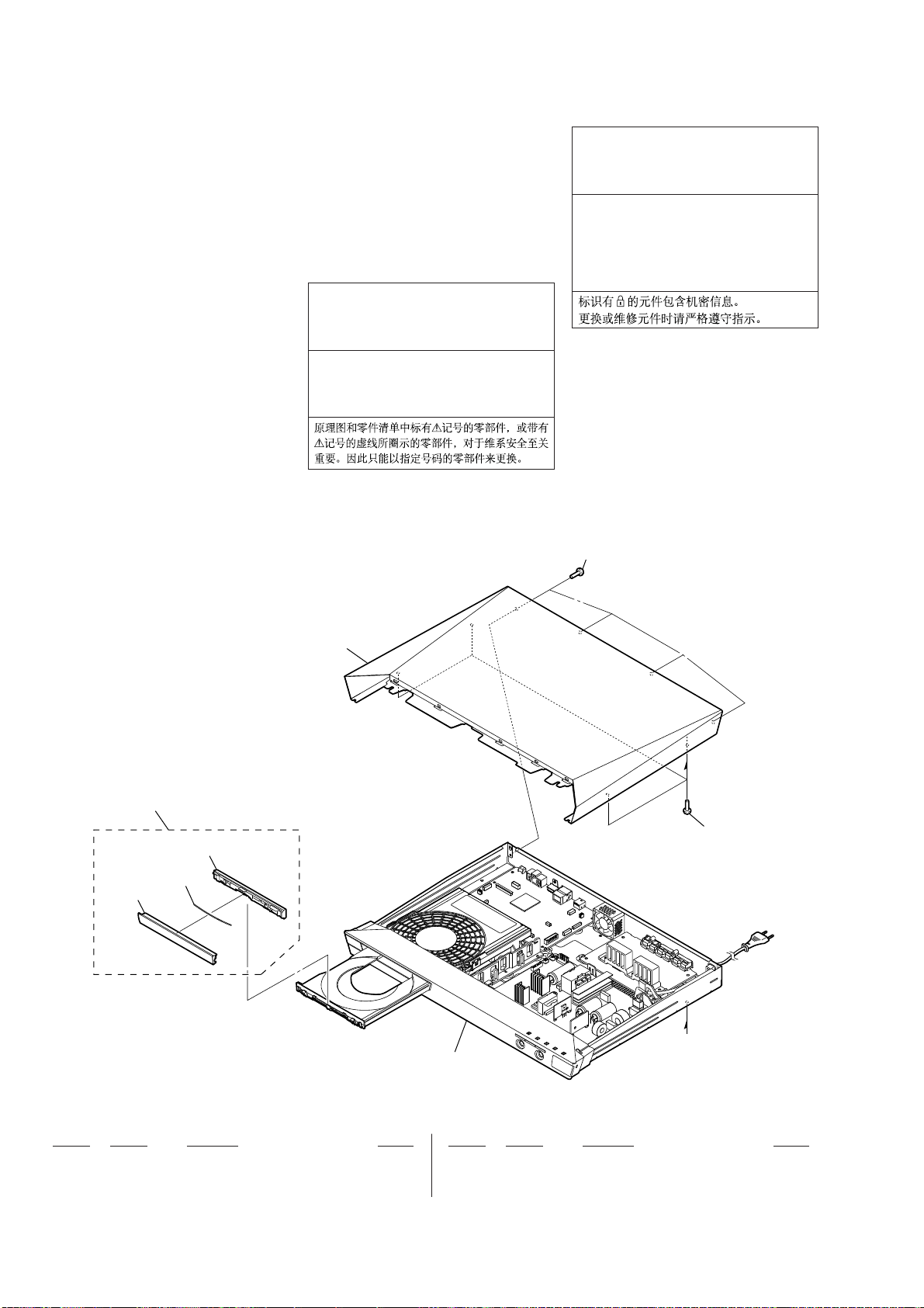
HBD-E2100/E3100/E3200/E4100/E6100
Ver. 1.7
SECTION 7
EXPLODED VIEWS
Note:
• -XX and -X mean standardized parts, so
they may have some difference from the
original one.
• Items marked “*” are not stocked since
they are seldom required for routine service. Some delay should be anticipated
when ordering these items.
• The mechanical parts with no reference
number in the exploded views are not supplied.
• Color Indication of Appearance Parts Example:
KNOB, BALANCE (WHITE) . . . (RED)
• Abbreviation
AR : Argentina model
AUS : Australian model
CH : Chinese model
CND : Canadian model
E3 : 240 V AC area in E model
E12 : 220 – 240 V AC area in E model
Parts Color Cabinet’s Color
E32 : 110 – 240 V AC area in E model
E51 : Chilean and Peruvian models
EA : Saudi Arabia model
MX6 : Latin-American model
PX : PX model
RU : Russian model
SAF : South African model
SP : Singapore model
TH : Thai model
TW : Taiwan model
The components identifi ed by mark 0
or dotted line with mark 0 are critical for
safety.
Replace only with part number specifi ed.
Les composants identifi és par une marque
0 sont critiques pour la sécurité.
Ne les remplacer que par une pièce portant le numéro spécifi é.
The components identifi ed by mark 9 con-
tain confi dential information.
Strictly follow the instructions whenever the
components are repaired and/or replaced.
Les composants identifi és par la marque
9 contiennent des informations confi den-
tielles.
Suivre scrupuleusement les instructions
chaque fois qu’un composant est remplacé
et / ou réparé.
7-1. CASE SECTION
3
not supplied
not supplied
4
1
2
A
1
A
front panel section
Ref. No. Part No. Description Remark Ref. No. Part No. Description Remark
1 3-077-331-71 +BV3 (3-CR)
2 4-438-897-02 CASE (US)
2 4-438-897-12 CASE (EXCEPT US)
3 X-2585-804-1 PANEL LOADING ASSY
4 4-295-431-01 SPRING, LOADING
76
Page 77
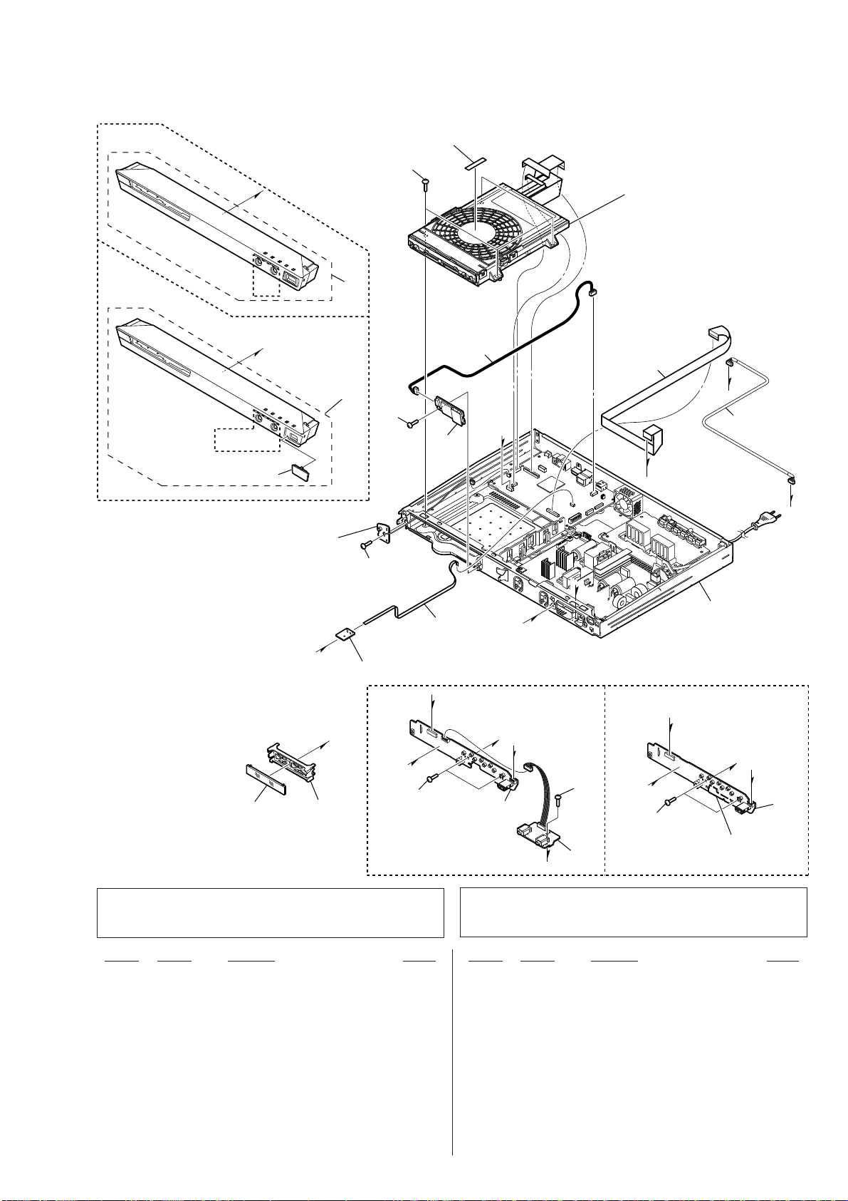
7-2. FRONT PANEL SECTION
HBD-E2100/E3100/E3200/E4100/E6100
Ver. 1.7
(E2100)
B
(SP)
(E3100/E4100/E6100)
B
(SP, RU)
not supplied
not supplied
(POWER KEY board)
51
51
not supplied
54
54
56
55
C
BD drive section
(BPX-7)
57
D
C
58
E
54
B
52
G
F
chassis bottom section
53
ND01
(SP, RU ) (EXCEPT SP, RU)
H
not supplied
H
54
D
F
59
E
54
H
D
F
E
59
54
not supplied
60
G
Note 1: When replacing the WLAN/BT COMBO card, refer to
“CHECKING METHOD OF NETWORK OPERATION”
(page 11).
Ref. No. Part No. Description Remark Ref. No. Part No. Description Remark
51 X-2585-795-2 FRONT PANEL ASSY (EJ1) (E2100: EXCEPT SP)
51 X-2585-796-2 FRONT PANEL ASSY (EJ1K) (E2100: SP)
51 X-2585-797-2 FRONT PANEL ASSY (EJ2)
(E3100: EXCEPT SP, RU)
51 X-2585-798-2 FRONT PANEL ASSY (EJ2K) (E3100: SP, RU)
51 X-2585-799-2 FRONT PANEL ASSY (EJ4)
(E4100: EXCEPT SP, RU)
51 X-2585-800-2 FRONT PANEL ASSY (EJ4K) (E4100: SP, RU)
51 X-2585-801-2 FRONT PANEL ASSY (EJ8)
(E6100: EXCEPT SP, RU)
51 X-2585-802-2 FRONT PANEL ASSY (EJ8K) (E6100: SP, RU)
51 X-2589-165-1 FRONT PANEL ASSY (EJ2) MK2 (E3200)
52 1-846-378-51 WIRE (FLAT TYPE) (8 CORE)
Note 2: Wires (fl at type) for service is all straight.
Please bend it referring go “HOW TO BEND FFC” on
page 14 when you install it in the unit.
53 8-989-470-05 RC-S801/A5 (WW)
54 3-077-331-71 +BV3 (3-CR)
55 1-968-687-12 HARNESS (USB)
56 1-458-601-11 CARD, WLAN/BT COMBO
57 1-846-376-61 WIRE (FLAT TYPE) (21 CORE) (SP, RU)
57 1-846-377-61 WIRE (FLAT TYPE) (15 CORE) (EXCEPT SP, RU)
58 1-969-958-11 HARNESS (USB)
59 A-1901-384-A PANEL BOARD, COMPLETE (EXCEPT SP, RU)
59 A-1901-496-A PANEL BOARD, COMPLETE (SP, RU)
60 A-1901-498-A KARAOKE BOARD, COMPLETE (SP, RU)
ND01 1-483-460-11 VACUUM FLUORESCENT DISPLAY
(NON-KARAOKE board)
77
Page 78
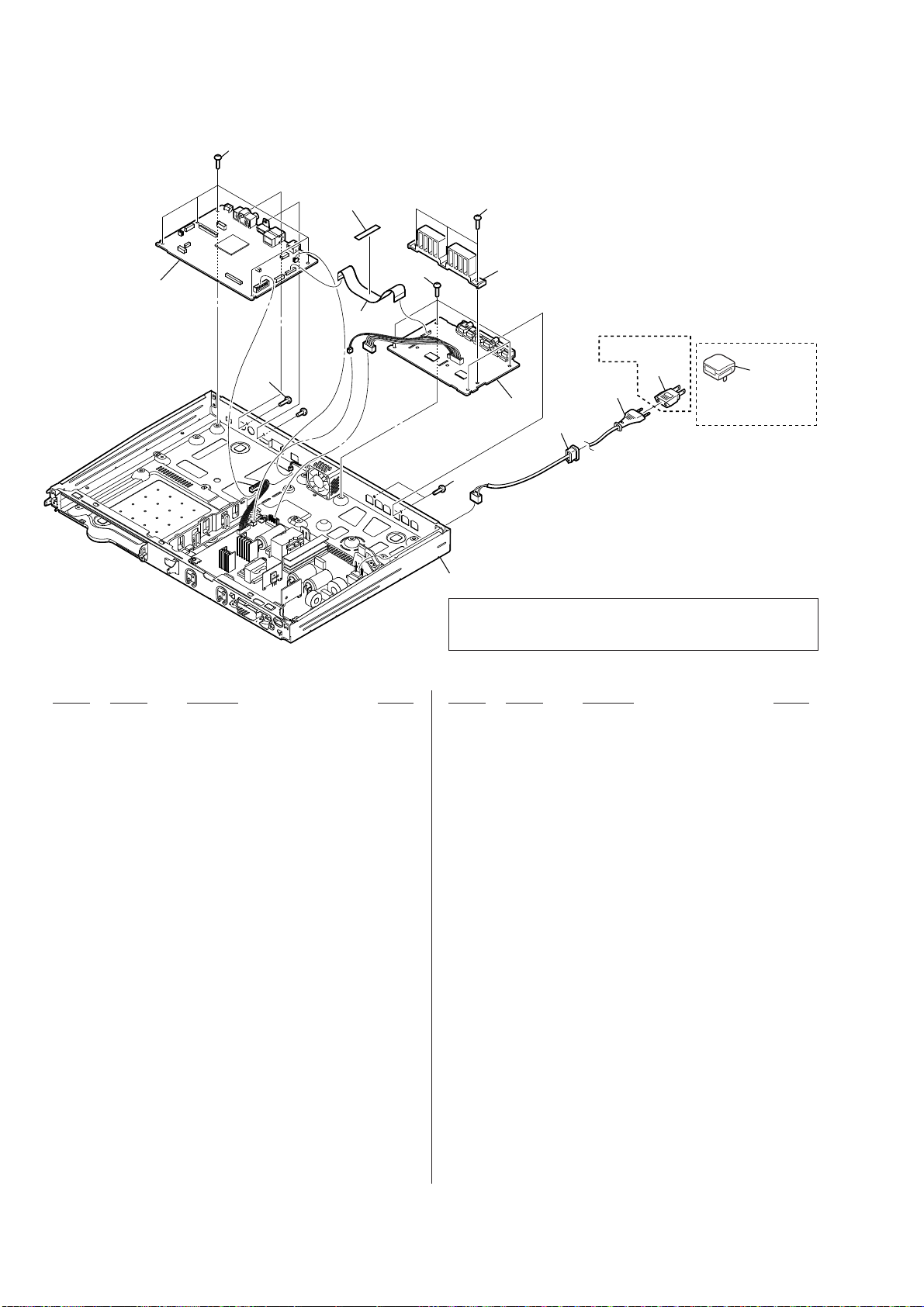
HBD-E2100/E3100/E3200/E4100/E6100
Ver. 1.7
7-3. CHASSIS BOTTOM SECTION
101
102
101
104
101
101
not supplied
105
(PX, MX6, E32)
108
#1
103
107
(E2100: SP for
Hong Kong model)
109
106
101
chassis section
Note: Wires (fl at type) for service is all straight.
Please bend it referring go “HOW TO BEND FFC” on page
14 when you install it in the unit.
Ref. No. Part No. Description Remark Ref. No. Part No. Description Remark
101 3-077-331-71 +BV3 (3-CR)
9 102 A-1901-414-A MB1002 BOARD, COMPLETE (for SERVICE)
(E2100: US)
9 102 A-1901-461-A MB1002 BOARD, COMPLETE (for SERVICE)
(E2100: CND)
9 102 A-1901-480-A MB1002 BOARD, COMPLETE (for SERVICE)
(E2100: AEP)
9 102 A-1901-487-A MB1002 BOARD, COMPLETE (for SERVICE)
(E2100: UK)
9 102 A-1901-506-A MB1002 BOARD, COMPLETE (for SERVICE)
(E2100: SAF)
9 102 A-1901-513-A MB1002 BOARD, COMPLETE (for SERVICE)
(E2100: SP)
9 102 A-1901-526-A MB1002 BOARD, COMPLETE (for SERVICE)
(E2100: AUS)
9 102 A-1901-532-A MB1002 BOARD, COMPLETE (for SERVICE)
(E2100: TW)
9 102 A-1901-538-A MB1002 BOARD, COMPLETE (for SERVICE)
(E2100: E51, MX6)
9 102 A-1901-565-A MB1002 BOARD, COMPLETE (for SERVICE)
(E3100: US)
9 102 A-1901-575-A MB1002 BOARD, COMPLETE (for SERVICE)
(E3100: CND)
9 102 A-1901-651-A MB1002 BOARD, COMPLETE (for SERVICE)
(E3100: E3)
9 102 A-1901-657-A MB1002 BOARD, COMPLETE (for SERVICE)
(E3100: SAF)
9 102 A-1901-689-A MB1002 BOARD, COMPLETE (for SERVICE)
(E3100: EA)
9 102 A-1901-764-A MB1002 BOARD, COMPLETE (for SERVICE)
(E3100: SP)
9 102 A-1901-794-A MB1002 BOARD, COMPLETE (for SERVICE)
(E3100: TH)
9 102 A-1901-800-A MB1002 BOARD, COMPLETE (for SERVICE)
(E3100: E32)
9 102 A-1902-052-A MB1002 BOARD, COMPLETE (for SERVICE)
(E4100: CND)
9 102 A-1902-058-A MB1002 BOARD, COMPLETE (for SERVICE)
(E4100: AEP)
9 102 A-1902-064-A MB1002 BOARD, COMPLETE (for SERVICE)
(E4100: UK)
9 102 A-1902-110-A MB1002 BOARD, COMPLETE (for SERVICE)
(E4100: RU)
9 102 A-1902-120-A MB1002 BOARD, COMPLETE (for SERVICE)
(E4100: E12)
9 102 A-1902-140-A MB1002 BOARD, COMPLETE (for SERVICE)
(E4100: E3)
9 102 A-1902-170-A MB1002 BOARD, COMPLETE (for SERVICE)
(E4100: EA)
9 102 A-1902-180-A MB1002 BOARD, COMPLETE (for SERVICE)
(E4100: SP)
9 102 A-1902-234-A MB1002 BOARD, COMPLETE (for SERVICE)
(E4100: CH)
9 102 A-1902-240-A MB1002 BOARD, COMPLETE (for SERVICE)
(E4100: TH)
9 102 A-1902-248-A MB1002 BOARD, COMPLETE (for SERVICE)
(E4100: TW)
9 102 A-1902-254-A MB1002 BOARD, COMPLETE (for SERVICE)
(E4100: E51, MX6)
78
– Continued on next page –
Page 79

Ref. No. Part No. Description Remark
9 102 A-1902-260-A MB1002 BOARD, COMPLETE (for SERVICE)
(E6100: CND)
9 102 A-1902-269-A MB1002 BOARD, COMPLETE (for SERVICE)
(E6100: AEP)
9 102 A-1902-276-A MB1002 BOARD, COMPLETE (for SERVICE)
(E6100: RU)
9 102 A-1902-311-A MB1002 BOARD, COMPLETE (for SERVICE)
(E6100: E3)
9 102 A-1902-325-A MB1002 BOARD, COMPLETE (for SERVICE)
(E6100: SAF)
HBD-E2100/E3100/E3200/E4100/E6100
Ver. 1.7
9 102 A-1902-337-A MB1002 BOARD, COMPLETE (for SERVICE)
(E6100: EA)
9 102 A-1902-343-A MB1002 BOARD, COMPLETE (for SERVICE)
(E6100: SP)
9 102 A-1902-351-A MB1002 BOARD, COMPLETE (for SERVICE)
(E6100: AUS)
9 102 A-1902-357-A MB1002 BOARD, COMPLETE (for SERVICE)
(E6100: TH)
9 102 A-1918-063-A MB1002 BOARD, COMPLETE (for SERVICE)
(E3100: UK)
9 102 A-1918-079-A MB1002 BOARD, COMPLETE (for SERVICE)
(E6100: TW)
9 102 A-1921-463-A MB1002 BOARD, COMPLETE (for SERVICE)
(E2100: PX)
9 102 A-1943-338-A MB1002 BOARD, COMPLETE (for SERVICE)
(E2100: E3)
9 102 A-1964-709-A MB1002 BOARD, COMPLETE (for SERVICE)
(E4100: AR)
9 102 A-1972-053-A MB1002 BOARD, COMPLETE (for SERVICE)
(E6100: CH)
9 102 A-1994-882-A MB1002 BOARD, COMPLETE (for SERVICE)
(E2100: AR)
9 102 A-2009-289-A MB1002 BOARD, COMPLETE (for SERVICE)
9 102 A-2045-555-A MB1002 BOARD, COMPLETE (for SERVICE)
(E3100: RU)
9 102 A-2060-242-A MB1002 BOARD, COMPLETE (for SERVICE)
(E4100: E51)
9 102 A-2060-250-A MB1002 BOARD, COMPLETE (for SERVICE)
(E2100: E51)
(E3200)
0 103 A-1901-382-A AMP BOARD, COMPLETE (EXCEPT US)
0 103 A-1924-824-A AMP BOARD, COMPLETE (US)
104 4-214-276-01 TAPE
105 1-846-375-51 WIRE (FLAT TYPE) (24 CORE)
0 106 4-966-267-12 BUSHING (FBS001), CORD
0 107 1-834-966-41 POWER-SUPPLY CORD
0 107 1-835-068-21 CORD, POWER (AUS)
0 107 1-837-308-11 CORD, POWER-SUPPLY (US, CND)
0 107 1-837-312-11 CORD, POWER-SUPPLY (AR)
0 107 1-837-345-11 CORD, POWER-SUPPLY (TW)
0 107 1-837-822-21 CORD, POWER-SUPPLY (CH)
0 107 1-839-012-11 CORD, POWER-SUPPLY (E12)
0 107 1-839-940-21 POWER-SUPPLY CORD (TH)
0 107 1-839-999-21 POWER-SUPPLY CORD (UK, EA)
0 108 1-785-504-21 ADAPTOR, CONVERSION (E51, PX, E32, MX6)
0 109 1-770-019-71 ADAPTOR, CONVERSION PLUG 3P
#1 7-682-546-09 SCREW +B 3X5
(AEP, E3, E51, SAF, SP, E32, RU, MX6, PX)
(E2100: SP for Hong Kong model)
79
Page 80
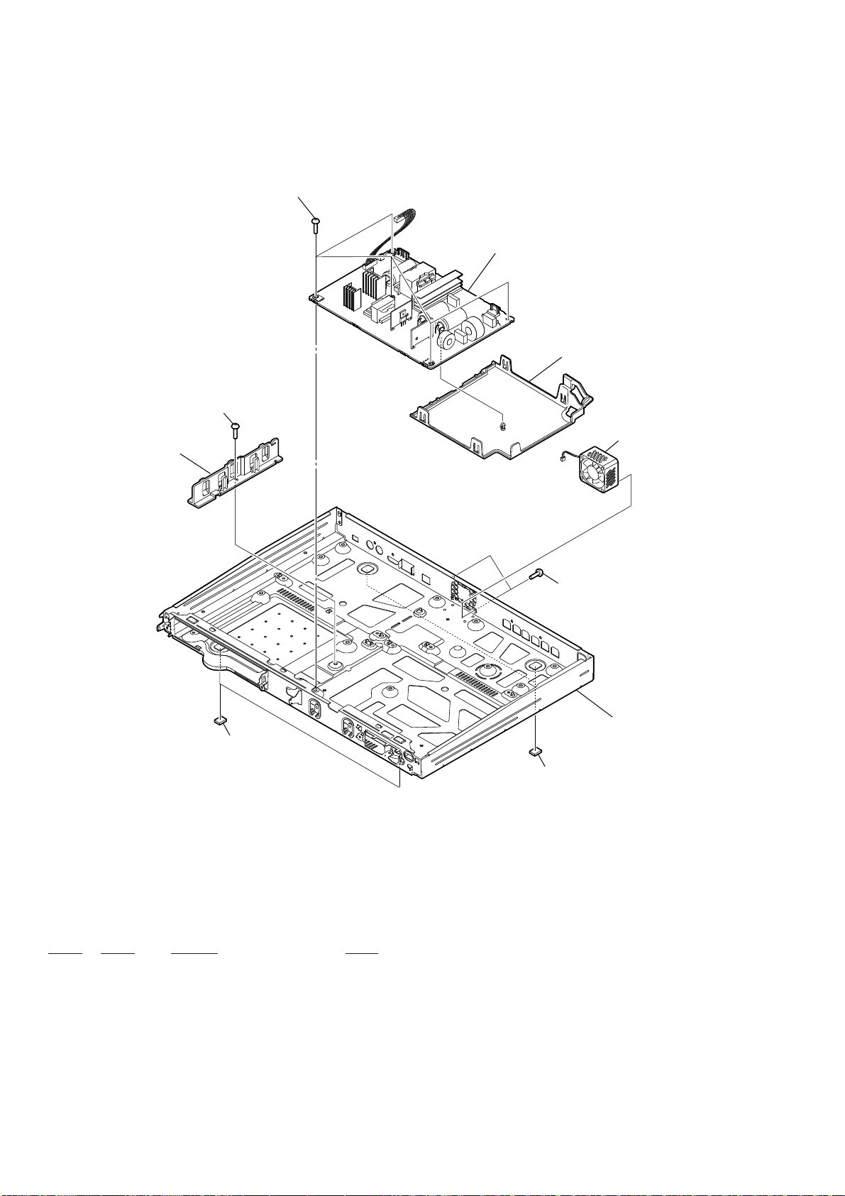
HBD-E2100/E3100/E3200/E4100/E6100
Ver. 1.7
7-4. CHASSIS SECTION
151
151
SWR1
not supplied
not supplied
M1
151
not supplied
152
152
Ref. No. Part No. Description Remark
151 3-077-331-71 +BV3 (3-CR)
152 4-295-590-01 FOOT
0 M1 1-855-244-11 DC FAN
0 SWR1 1-798-453-11 SWITCHING REGULATOR (3L392W-1)
0 SWR1 1-798-453-21 SWITCHING REGULATOR (3L392W)
(US, CND, AEP, UK, SAF, SP, TW, AUS, TH, CH)
(E3, E51, PX, EA, E12, E32, RU, MX6, AR)
80
Page 81
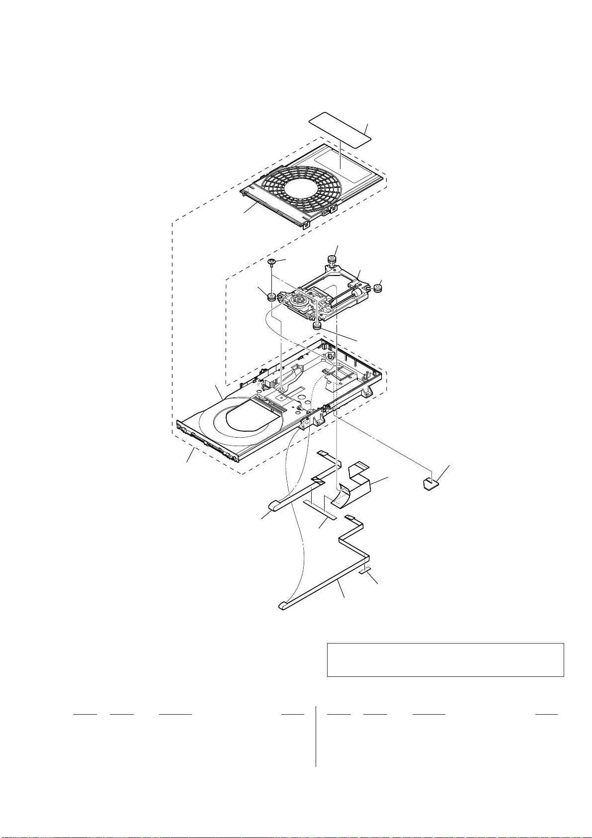
7-5. BD DRIVE SECTION (BPX-7)
not supplied
HBD-E2100/E3100/E3200/E4100/E6100
Ver. 1.5
not supplied
204
not supplied
202
204
206
203
205
204
204
201
207
not
supplied
not supplied
208
Note: Wires (fl at type) for service is all straight.
Please bend it referring go “HOW TO BEND FFC” on page
14 when you install it in the unit.
Ref. No. Part No. Description Remark Ref. No. Part No. Description Remark
201 4-295-426-01 COVER, DRIVE
202 A-1850-153-D LOADING FOR SERVICE (BPX-7)
203 2-345-115-01 SCREW (S), FLOAT
204 4-175-937-31 INSULATOR
0 205 8-820-452-07 DEVICE, OPTICAL KEM480AAA/C2RP2
206 1-846-349-61 WIRE (FLAT TYPE) (9 CORE)
207 1-846-347-11 FLEXIBLE FLAT CABLE (45 CORE)
208 1-846-348-61 WIRE (FLAT TYPE) (5 CORE)
81
Page 82
HBD-E2100/E3100/E3200/E4100/E6100
Ver. 1.7
AMP
Note:
• Due to standardization, replacements in
the parts list may be different from the
parts specifi ed in the diagrams or the com-
ponents used on the set.
• -XX and -X mean standardized parts, so
they may have some difference from the
original one.
• Items marked “*” are not stocked since
they are seldom required for routine service. Some delay should be anticipated
when ordering these items.
• RESISTORS
All resistors are in ohms.
METAL: Metal-fi lm resistor.
METAL OXIDE: Metal oxide-fi lm resistor.
F: nonfl ammable
• CAPACITORS
uF: μF
• COILS
uH: μH
ELECTRICAL PARTS LIST
• SEMICONDUCTORS
In each case, u: μ, for example:
uA. . : μA. . , uPA. . , μPA. . ,
uPB. . : μPB. . , uPC. . , μPC. . ,
uPD. . : μPD. .
• Abbreviation
AR : Argentina model
AUS : Australian model
CH : Chinese model
CND : Canadian model
E3 : 240 V AC area in E model
E12 : 220 – 240 V AC area in E model
E32 : 110 – 240 V AC area in E model
E51 : Chilean and Peruvian models
EA : Saudi Arabia model
MX6 : Latin-American model
PX : PX model
RU : Russian model
SAF : South African model
SP : Singapore model
TH : Thai model
TW : Taiwan model
When indicating parts by reference number, please include the board name.
SECTION 8
The components identifi ed by mark 0
or dotted line with mark 0 are critical for
safety.
Replace only with part number specifi ed.
Les composants identifi és par une marque
0 sont critiques pour la sécurité.
Ne les remplacer que par une pièce portant le numéro spécifi é.
The components identifi ed by mark 9 con-
tain confi dential information.
Strictly follow the instructions whenever the
components are repaired and/or replaced.
Les composants identifi és par la marque
9 contiennent des informations confi den-
tielles.
Suivre scrupuleusement les instructions
chaque fois qu’un composant est remplacé
et / ou réparé.
Ref. No. Part No. Description Remark Ref. No. Part No. Description Remark
0 A-1901-382-A AMP BOARD, COMPLETE (EXCEPT US)
0 A-1924-824-A AMP BOARD, COMPLETE (US)
********************
< CAPACITOR >
C3013 1-116-717-11 CERAMIC CHIP 10uF 20% 10V
C3014 1-118-668-11 CERAMIC CHIP 0.1uF 10% 50V
C3021 1-116-717-11 CERAMIC CHIP 10uF 20% 10V
C3022 1-116-717-11 CERAMIC CHIP 10uF 20% 10V
C3023 1-116-717-11 CERAMIC CHIP 10uF 20% 10V
C3025 1-118-668-11 CERAMIC CHIP 0.1uF 10% 50V
C3026 1-118-388-11 CERAMIC CHIP 0.047uF 10% 25V
C3027 1-118-689-81 CERAMIC CHIP 0.0047uF 5% 10V
C3028 1-118-388-11 CERAMIC CHIP 0.047uF 10% 25V
C3029 1-118-689-81 CERAMIC CHIP 0.0047uF 5% 10V
C3031 1-118-668-11 CERAMIC CHIP 0.1uF 10% 50V
C3032 1-118-668-11 CERAMIC CHIP 0.1uF 10% 50V
C3033 1-118-668-11 CERAMIC CHIP 0.1uF 10% 50V
C3041 1-118-668-11 CERAMIC CHIP 0.1uF 10% 50V
C3042 1-118-668-11 CERAMIC CHIP 0.1uF 10% 50V
C3050 1-165-979-21 ELECT CHIP 100uF 20% 6.3V
C3051 1-164-232-91 CERAMIC CHIP 0.01uF 10% 100V
C3099 1-118-691-11 CERAMIC CHIP 2.2uF 10% 100V
C3106 1-118-698-11 CERAMIC CHIP 0.1uF 10% 100V
C3107 1-118-698-11 CERAMIC CHIP 0.1uF 10% 100V
C3133 1-116-717-11 CERAMIC CHIP 10uF 20% 10V
C3134 1-118-698-11 CERAMIC CHIP 0.1uF 10% 100V
C3135 1-118-698-11 CERAMIC CHIP 0.1uF 10% 100V
C3136 1-118-668-11 CERAMIC CHIP 0.1uF 10% 50V
C3138 1-118-668-11 CERAMIC CHIP 0.1uF 10% 50V
C3139 1-118-668-11 CERAMIC CHIP 0.1uF 10% 50V
C3140 1-100-158-91 CERAMIC CHIP 1000PF 5% 100V
C3141 1-100-158-91 CERAMIC CHIP 1000PF 5% 100V
C3151 1-118-470-31 ELECT 560uF 20% 35V
C3152 1-118-470-31 ELECT 560uF 20% 35V
C3153 1-118-470-31 ELECT 560uF 20% 35V
C3154 1-118-470-31 ELECT 560uF 20% 35V
C3156 1-118-698-11 CERAMIC CHIP 0.1uF 10% 100V
C3157 1-118-698-11 CERAMIC CHIP 0.1uF 10% 100V
* C3228 1-116-720-11 CERAMIC CHIP 10uF 20% 6.3V
C3251 1-118-122-11 ELECT 270uF 20% 63V (US)
C3251 1-118-453-31 ELECT 270uF 20% 63V
(EXCEPT US)
C3253 1-118-122-11 ELECT 270uF 20% 63V (US)
C3253 1-118-453-31 ELECT 270uF 20% 63V
(EXCEPT US)
C3271 1-100-154-91 CERAMIC CHIP 330PF 5% 100V
C3272 1-100-154-91 CERAMIC CHIP 330PF 5% 100V
C3281 1-100-154-91 CERAMIC CHIP 330PF 5% 100V
C3282 1-100-154-91 CERAMIC CHIP 330PF 5% 100V
C3108 1-118-691-11 CERAMIC CHIP 2.2uF 10% 100V
C3109 1-118-691-11 CERAMIC CHIP 2.2uF 10% 100V
C3115 1-118-668-11 CERAMIC CHIP 0.1uF 10% 50V
C3117 1-100-158-91 CERAMIC CHIP 1000PF 5% 100V
C3118 1-118-691-11 CERAMIC CHIP 2.2uF 10% 100V
C3119 1-118-691-11 CERAMIC CHIP 2.2uF 10% 100V
C3120 1-100-158-91 CERAMIC CHIP 1000PF 5% 100V
C3122 1-118-668-11 CERAMIC CHIP 0.1uF 10% 50V
C3123 1-114-920-21 CERAMIC CHIP 0.47uF 10% 250V
C3124 1-114-920-21 CERAMIC CHIP 0.47uF 10% 250V
C3127 1-116-731-11 CERAMIC CHIP 2.2uF 20% 6.3V
C3131 1-116-717-11 CERAMIC CHIP 10uF 20% 10V
Note: When the AMP board is replaced, spread the compound referring to “NOTE OF
REPLACING THE IC3102 AND IC3302 ON THE AMP BOARD AND THE
COMPLETE AMP BOARD” on servicing notes (page 10).
C3306 1-118-698-11 CERAMIC CHIP 0.1uF 10% 100V
C3307 1-118-698-11 CERAMIC CHIP 0.1uF 10% 100V
C3308 1-118-691-11 CERAMIC CHIP 2.2uF 10% 100V
C3309 1-118-691-11 CERAMIC CHIP 2.2uF 10% 100V
C3315 1-118-668-11 CERAMIC CHIP 0.1uF 10% 50V
C3317 1-100-158-91 CERAMIC CHIP 1000PF 5% 100V
C3318 1-118-691-11 CERAMIC CHIP 2.2uF 10% 100V
C3319 1-118-691-11 CERAMIC CHIP 2.2uF 10% 100V
C3320 1-118-668-11 CERAMIC CHIP 0.1uF 10% 50V
C3322 1-100-158-91 CERAMIC CHIP 1000PF 5% 100V
C3323 1-114-920-21 CERAMIC CHIP 0.47uF 10% 250V
C3324 1-114-920-21 CERAMIC CHIP 0.47uF 10% 250V
82
Page 83
HBD-E2100/E3100/E3200/E4100/E6100
Ver. 1.5
AMP
Ref. No. Part No. Description Remark Ref. No. Part No. Description Remark
C3328 1-116-731-11 CERAMIC CHIP 2.2uF 20% 6.3V
C3331 1-116-717-11 CERAMIC CHIP 10uF 20% 10V
C3333 1-116-717-11 CERAMIC CHIP 10uF 20% 10V
D3103 6-503-967-01 DI STPS1H100A
D3104 6-503-967-01 DI STPS1H100A
D3105 6-503-967-01 DI STPS1H100A
C3334 1-118-698-11 CERAMIC CHIP 0.1uF 10% 100V
C3335 1-118-698-11 CERAMIC CHIP 0.1uF 10% 100V
C3336 1-118-668-11 CERAMIC CHIP 0.1uF 10% 50V
C3338 1-118-668-11 CERAMIC CHIP 0.1uF 10% 50V
C3339 1-118-668-11 CERAMIC CHIP 0.1uF 10% 50V
C3340 1-100-158-91 CERAMIC CHIP 1000PF 5% 100V
C3341 1-100-158-91 CERAMIC CHIP 1000PF 5% 100V
C3351 1-118-470-31 ELECT 560uF 20% 35V
C3352 1-118-470-31 ELECT 560uF 20% 35V
C3353 1-118-470-31 ELECT 560uF 20% 35V
C3354 1-118-470-31 ELECT 560uF 20% 35V
C3356 1-118-698-11 CERAMIC CHIP 0.1uF 10% 100V
C3357 1-118-698-11 CERAMIC CHIP 0.1uF 10% 100V
C3371 1-100-154-91 CERAMIC CHIP 330PF 5% 100V
C3372 1-100-154-91 CERAMIC CHIP 330PF 5% 100V
C3381 1-100-154-91 CERAMIC CHIP 330PF 5% 100V
C3382 1-100-154-91 CERAMIC CHIP 330PF 5% 100V
C3401 1-164-232-91 CERAMIC CHIP 0.01uF 10% 100V
C3402 1-100-158-91 CERAMIC CHIP 1000PF 5% 100V
C3403 1-164-232-91 CERAMIC CHIP 0.01uF 10% 100V
C3404 1-100-158-91 CERAMIC CHIP 1000PF 5% 100V
C3405 1-164-232-91 CERAMIC CHIP 0.01uF 10% 100V
C3406 1-100-158-91 CERAMIC CHIP 1000PF 5% 100V
C3407 1-164-232-91 CERAMIC CHIP 0.01uF 10% 100V
C3408 1-100-158-91 CERAMIC CHIP 1000PF 5% 100V
C3451 1-164-232-91 CERAMIC CHIP 0.01uF 10% 100V
C3452 1-164-232-91 CERAMIC CHIP 0.01uF 10% 100V
C3453 1-100-158-91 CERAMIC CHIP 1000PF 5% 100V
C3454 1-100-158-91 CERAMIC CHIP 1000PF 5% 100V
C3455 1-164-232-91 CERAMIC CHIP 0.01uF 10% 100V
C3456 1-164-232-91 CERAMIC CHIP 0.01uF 10% 100V
C3457 1-100-158-91 CERAMIC CHIP 1000PF 5% 100V
C3458 1-100-158-91 CERAMIC CHIP 1000PF 5% 100V
C3459 1-164-232-91 CERAMIC CHIP 0.01uF 10% 100V
C3460 1-164-232-91 CERAMIC CHIP 0.01uF 10% 100V
C3461 1-100-158-91 CERAMIC CHIP 1000PF 5% 100V
C3462 1-100-158-91 CERAMIC CHIP 1000PF 5% 100V
C3463 1-164-232-91 CERAMIC CHIP 0.01uF 10% 100V
C3464 1-164-232-91 CERAMIC CHIP 0.01uF 10% 100V
C3465 1-100-158-91 CERAMIC CHIP 1000PF 5% 100V
C3466 1-100-158-91 CERAMIC CHIP 1000PF 5% 100V
C3552 1-126-208-21 ELECT CHIP 47uF 20% 4V
C3554 1-116-405-11 CERAMIC CHIP 0.01uF 10% 100V
C3555 1-118-668-11 CERAMIC CHIP 0.1uF 10% 50V
C3557 1-112-777-11 CERAMIC CHIP 0.01uF 10% 25V
C3570 1-100-908-11 CERAMIC CHIP 1uF 10% 6.3V
C3949 1-114-920-21 CERAMIC CHIP 0.47uF 10% 250V
C3950 1-114-920-21 CERAMIC CHIP 0.47uF 10% 250V
C3951 1-114-920-21 CERAMIC CHIP 0.47uF 10% 250V
C3952 1-114-920-21 CERAMIC CHIP 0.47uF 10% 250V
< CONNECTOR >
CN3505 1-815-763-32 CONNECTOR, FFC/FPC 24P
< DIODE >
D3101 6-503-967-01 DI STPS1H100A
D3102 6-503-967-01 DI STPS1H100A
Note: When the IC3102 and IC3302 on the AMP board are replaced, spread the
compound referring to “NOTE OF REPLACING THE IC3102 and IC3302 ON THE
AMP BOARD AND THE COMPLETE AMP BOARD” on servicing notes (page 10).
D3106 6-503-967-01 DI STPS1H100A
D3107 6-503-967-01 DI STPS1H100A
D3108 6-503-967-01 DI STPS1H100A
D3151 6-503-761-01 DI RB751S40, 115
D3301 6-503-967-01 DI STPS1H100A
D3302 6-503-967-01 DI STPS1H100A
D3303 6-503-967-01 DI STPS1H100A
D3304 6-503-967-01 DI STPS1H100A
D3305 6-503-967-01 DI STPS1H100A
D3306 6-503-967-01 DI STPS1H100A
D3307 6-503-967-01 DI STPS1H100A
D3308 6-503-967-01 DI STPS1H100A
D3351 6-503-761-01 DI RB751S40, 115
D3503 6-503-761-01 DI RB751S40, 115
< IC >
IC3001 6-718-103-01 IC TAS5538DGGR
IC3102 6-719-138-01 IC STA516BF13TR-A
IC3302 6-719-138-01 IC STA516BF13TR-A
< COIL >
L3051 1-400-791-21 INDUCTOR 10uH
L3101 1-482-176-11 INDUCTOR 20uH
L3103 1-482-176-11 INDUCTOR 20uH
L3301 1-482-176-11 INDUCTOR 20uH
L3303 1-482-176-11 INDUCTOR 20uH
< TRANSISTOR >
Q3101 8-729-013-22 TR HN1A01FU
Q3202 8-729-013-22 TR HN1A01FU
Q3302 8-729-013-22 TR HN1A01FU
Q3552 8-729-427-72 TRANSISTOR XP4501
Q3553 6-552-892-01 TR LSCR523UBFS8TL
Q3555 8-729-013-22 TR HN1A01FU
< RESISTOR >
R3021 1-218-968-11 METAL CHIP 18K 5% 1/16W
R3022 1-218-967-11 METAL CHIP 15K 5% 1/16W
R3023 1-218-949-11 METAL CHIP 470 5% 1/16W
R3024 1-218-949-11 METAL CHIP 470 5% 1/16W
R3032 1-216-295-91 SHORT CHIP 0
R3033 1-218-965-11 METAL CHIP 10K 5% 1/16W
R3041 1-218-937-11 METAL CHIP 47 5% 1/16W
R3051 1-216-845-11 METAL CHIP 100K 5% 1/10W
R3059 1-218-965-11 METAL CHIP 10K 5% 1/16W
R3060 1-218-965-11 METAL CHIP 10K 5% 1/16W
R3061 1-218-965-11 METAL CHIP 10K 5% 1/16W
R3062 1-218-965-11 METAL CHIP 10K 5% 1/16W
R3072 1-218-937-11 METAL CHIP 47 5% 1/16W
R3073 1-218-937-11 METAL CHIP 47 5% 1/16W
R3109 1-218-977-11 METAL CHIP 100K 5% 1/16W
R3153 1-220-281-11 METAL CHIP 4.7K 5% 1/4W
R3154 1-220-281-11 METAL CHIP 4.7K 5% 1/4W
R3155 1-220-281-11 METAL CHIP 4.7K 5% 1/4W
R3156 1-220-281-11 METAL CHIP 4.7K 5% 1/4W
R3161 1-218-965-11 METAL CHIP 10K 5% 1/16W
R3162 1-218-965-11 METAL CHIP 10K 5% 1/16W
83
Page 84

HBD-E2100/E3100/E3200/E4100/E6100
Ver. 1.5
AMP
Ref. No. Part No. Description Remark Ref. No. Part No. Description Remark
R3212 1-218-977-11 METAL CHIP 100K 5% 1/16W
R3271 1-218-282-11 METAL CHIP 22 5% 1/2W
R3272 1-218-282-11 METAL CHIP 22 5% 1/2W
R3281 1-218-282-11 METAL CHIP 22 5% 1/2W
R3282 1-218-282-11 METAL CHIP 22 5% 1/2W
R3312 1-218-977-11 METAL CHIP 100K 5% 1/16W
R3353 1-220-281-11 METAL CHIP 4.7K 5% 1/4W
R3354 1-220-281-11 METAL CHIP 4.7K 5% 1/4W
R3355 1-220-281-11 METAL CHIP 4.7K 5% 1/4W
R3356 1-220-281-11 METAL CHIP 4.7K 5% 1/4W
R3361 1-218-965-11 METAL CHIP 10K 5% 1/16W
R3371 1-218-282-11 METAL CHIP 22 5% 1/2W
R3372 1-218-282-11 METAL CHIP 22 5% 1/2W
R3381 1-218-282-11 METAL CHIP 22 5% 1/2W
R3382 1-218-282-11 METAL CHIP 22 5% 1/2W
R3555 1-218-973-11 METAL CHIP 47K 5% 1/16W
R3556 1-218-969-11 METAL CHIP 22K 5% 1/16W
R3557 1-208-927-11 METAL CHIP 47K 0.5% 1/16W
R3558 1-208-911-11 METAL CHIP 10K 0.5% 1/16W
KARAOKE MB1002
C82 1-118-290-11 CERAMIC CHIP 0.001uF 10% 50V
* C84 1-118-360-11 CERAMIC CHIP 0.1uF 10% 25V
C85 1-116-734-11 CERAMIC CHIP 1uF 20% 16V
C86 1-118-040-11 CERAMIC CHIP 2.2uF 10% 16V
* C87 1-116-720-11 CERAMIC CHIP 10uF 20% 6.3V
* C88 1-116-720-11 CERAMIC CHIP 10uF 20% 6.3V
* C89 1-118-360-11 CERAMIC CHIP 0.1uF 10% 25V
C93 1-118-040-11 CERAMIC CHIP 2.2uF 10% 16V
C94 1-164-388-91 CERAMIC CHIP 270PF 5% 50V
C95 1-118-040-11 CERAMIC CHIP 2.2uF 10% 16V
< DIODE >
D71 6-500-400-01 DIODE BAV99-215
< IC >
IC71 6-713-989-01 IC NJM2783V (TE2)
IC72 6-718-174-01 IC NJU72341V (TE2)
< JACK >
R3559 1-208-683-11 METAL CHIP 1K 0.5% 1/16W
R3560 1-218-977-11 METAL CHIP 100K 5% 1/16W
R3902 1-216-839-11 METAL CHIP 33K 5% 1/10W
R3903 1-216-839-11 METAL CHIP 33K 5% 1/10W
R3904 1-216-839-11 METAL CHIP 33K 5% 1/10W
R3905 1-216-839-11 METAL CHIP 33K 5% 1/10W
R3906 1-216-839-11 METAL CHIP 33K 5% 1/10W
R3907 1-216-839-11 METAL CHIP 33K 5% 1/10W
R3908 1-216-839-11 METAL CHIP 33K 5% 1/10W
R3909 1-216-839-11 METAL CHIP 33K 5% 1/10W
< COMPOSITION CIRCUIT BLOCK >
RB3001 1-234-372-11 RES, NETWORK 100 (1005X4)
RB3002 1-234-372-11 RES, NETWORK 100 (1005X4)
RB3003 1-234-371-11 RES, NETWORK 47 (1005X4)
RB3102 1-234-371-11 RES, NETWORK 47 (1005X4)
RB3302 1-234-371-11 RES, NETWORK 47 (1005X4)
RB3303 1-234-381-11 RES, NETWORK 100K (1005X4)
RB3304 1-234-381-11 RES, NETWORK 100K (1005X4)
RB3305 1-234-381-11 RES, NETWORK 100K (1005X4)
< TERMINAL >
TB3401 1-780-452-11 TERMINAL BOARD (SPEAKER) 2P
(SPEAKERS SUR R/SUR L)
TB3451 1-780-951-11 TERMINAL BOARD (SPEAKER) 4P
(SPEAKERS FRONT R/FRONT L/SUBWOOFER/
CENTER)
************************************************************
A-1901-498-A KARAOKE BOARD, COMPLETE (SP, RU)
************************
< CAPACITOR >
C71 1-118-290-11 CERAMIC CHIP 0.001uF 10% 50V
C73 1-118-290-11 CERAMIC CHIP 0.001uF 10% 50V
C74 1-116-743-11 CERAMIC CHIP 0.22uF 10% 16V
C75 1-118-290-11 CERAMIC CHIP 0.001uF 10% 50V
C76 1-116-743-11 CERAMIC CHIP 0.22uF 10% 16V
C77 1-116-734-11 CERAMIC CHIP 1uF 20% 16V
C78 1-116-724-11 CERAMIC CHIP 4.7uF 20% 6.3V
* C79 1-116-720-11 CERAMIC CHIP 10uF 20% 6.3V
* C80 1-116-720-11 CERAMIC CHIP 10uF 20% 6.3V
* C81 1-118-360-11 CERAMIC CHIP 0.1uF 10% 25V
J71 1-794-702-11 JACK, HEADPHONE (MIC 1)
J72 1-794-702-11 JACK, HEADPHONE (MIC 2)
< JUMPER WIRE >
JW52 1-216-295-91 SHORT CHIP 0
JW53 1-216-296-11 SHORT CHIP 0
< RESISTOR >
R71 1-216-845-11 METAL CHIP 100K 5% 1/10W
R72 1-216-821-11 METAL CHIP 1K 5% 1/10W
R73 1-216-845-11 METAL CHIP 100K 5% 1/10W
R74 1-216-821-11 METAL CHIP 1K 5% 1/10W
R75 1-216-821-11 METAL CHIP 1K 5% 1/10W
R76 1-216-841-11 METAL CHIP 47K 5% 1/10W
R77 1-216-833-11 METAL CHIP 10K 5% 1/10W
R78 1-216-857-11 METAL CHIP 1M 5% 1/10W
R79 1-216-838-11 METAL CHIP 27K 5% 1/10W
R80 1-216-835-11 METAL CHIP 15K 5% 1/10W
R81 1-216-832-11 METAL CHIP 8.2K 5% 1/10W
R82 1-216-864-11 SHORT CHIP 0
R84 1-216-809-11 METAL CHIP 100 5% 1/10W
R85 1-216-809-11 METAL CHIP 100 5% 1/10W
R86 1-216-296-11 SHORT CHIP 0
R87 1-216-809-11 METAL CHIP 100 5% 1/10W
R88 1-216-817-11 METAL CHIP 470 5% 1/10W
************************************************************
9 A-1901-414-A MB1002 BOARD, COMPLETE (for SERVICE)
(E2100: US)
9 A-1901-461-A MB1002 BOARD, COMPLETE (for SERVICE)
(E2100: CND)
9 A-1901-480-A MB1002 BOARD, COMPLETE (for SERVICE)
(E2100: AEP)
9 A-1901-487-A MB1002 BOARD, COMPLETE (for SERVICE)
(E2100: UK)
9 A-1901-506-A MB1002 BOARD, COMPLETE (for SERVICE)
(E2100: SAF)
9 A-1901-513-A MB1002 BOARD, COMPLETE (for SERVICE)
(E2100: SP)
9 A-1901-526-A MB1002 BOARD, COMPLETE (for SERVICE)
(E2100: AUS)
9 A-1901-532-A MB1002 BOARD, COMPLETE (for SERVICE)
(E2100: TW)
84
Page 85

HBD-E2100/E3100/E3200/E4100/E6100
Ver. 1.7
MB1002
Ref. No. Part No. Description Remark Ref. No. Part No. Description Remark
9 A-1901-538-A MB1002 BOARD, COMPLETE (for SERVICE)
(E2100: E51, MX6)
9 A-1901-565-A MB1002 BOARD, COMPLETE (for SERVICE)
(E3100: US)
9 A-1901-575-A MB1002 BOARD, COMPLETE (for SERVICE)
(E3100: CND)
9 A-1901-651-A MB1002 BOARD, COMPLETE (for SERVICE)
(E3100: E3)
9 A-1901-657-A MB1002 BOARD, COMPLETE (for SERVICE)
(E3100: SAF)
9 A-1901-689-A MB1002 BOARD, COMPLETE (for SERVICE)
(E3100: EA)
9 A-1901-764-A MB1002 BOARD, COMPLETE (for SERVICE)
(E3100: SP)
9 A-1901-794-A MB1002 BOARD, COMPLETE (for SERVICE)
(E3100: TH)
9 A-1901-800-A MB1002 BOARD, COMPLETE (for SERVICE)
(E3100: E32)
9 A-1902-052-A MB1002 BOARD, COMPLETE (for SERVICE)
(E4100: CND)
9 A-1902-058-A MB1002 BOARD, COMPLETE (for SERVICE)
(E4100: AEP)
9 A-1902-064-A MB1002 BOARD, COMPLETE (for SERVICE)
(E4100: UK)
9 A-1902-110-A MB1002 BOARD, COMPLETE (for SERVICE)
(E4100: RU)
9 A-1902-120-A MB1002 BOARD, COMPLETE (for SERVICE)
(E4100: E12)
9 A-1902-140-A MB1002 BOARD, COMPLETE (for SERVICE)
(E4100: E3)
9 A-1902-170-A MB1002 BOARD, COMPLETE (for SERVICE)
(E4100: EA)
9 A-1902-180-A MB1002 BOARD, COMPLETE (for SERVICE)
(E4100: SP)
9 A-1902-234-A MB1002 BOARD, COMPLETE (for SERVICE)
(E4100: CH)
9 A-1902-240-A MB1002 BOARD, COMPLETE (for SERVICE)
(E4100: TH)
9 A-1902-248-A MB1002 BOARD, COMPLETE (for SERVICE)
(E4100: TW)
9 A-1902-254-A MB1002 BOARD, COMPLETE (for SERVICE)
(E4100: E51, MX6)
9 A-1902-260-A MB1002 BOARD, COMPLETE (for SERVICE)
(E6100: CND)
9 A-1902-269-A MB1002 BOARD, COMPLETE (for SERVICE)
(E6100: AEP)
9 A-1902-276-A MB1002 BOARD, COMPLETE (for SERVICE)
(E6100: RU)
9 A-1902-311-A MB1002 BOARD, COMPLETE (for SERVICE)
(E6100: E3)
9 A-1902-325-A MB1002 BOARD, COMPLETE (for SERVICE)
(E6100: SAF)
9 A-1902-337-A MB1002 BOARD, COMPLETE (for SERVICE)
(E6100: EA)
9 A-1902-343-A MB1002 BOARD, COMPLETE (for SERVICE)
(E6100: SP)
9 A-1902-351-A MB1002 BOARD, COMPLETE (for SERVICE)
(E6100: AUS)
9 A-1902-357-A MB1002 BOARD, COMPLETE (for SERVICE)
(E6100: TH)
9 A-1918-063-A MB1002 BOARD, COMPLETE (for SERVICE)
(E3100: UK)
9 A-1918-079-A MB1002 BOARD, COMPLETE (for SERVICE)
(E6100: TW)
9 A-1921-463-A MB1002 BOARD, COMPLETE (for SERVICE)
9 A-1943-338-A MB1002 BOARD, COMPLETE (for SERVICE)
A-1964-709-A MB1002 BOARD, COMPLETE (for SERVICE)
9
9 A-1972-053-A MB1002 BOARD, COMPLETE (for SERVICE)
9 A-1994-882-A MB1002 BOARD, COMPLETE (for SERVICE)
9 A-2009-289-A MB1002 BOARD, COMPLETE (for SERVICE)
9 A-2045-555-A MB1002 BOARD, COMPLETE (for SERVICE)
9 A-2060-242-A MB1002 BOARD, COMPLETE (for SERVICE)
9 A-2060-250-A MB1002 BOARD, COMPLETE (for SERVICE)
****************************
< CAPACITOR >
C108 1-118-386-11 CERAMIC CHIP 0.1uF 10% 16V
C109 1-118-386-11 CERAMIC CHIP 0.1uF 10% 16V
C115 1-118-386-11 CERAMIC CHIP 0.1uF 10% 16V
C118 1-118-386-11 CERAMIC CHIP 0.1uF 10% 16V
C120 1-118-386-11 CERAMIC CHIP 0.1uF 10% 16V
C121 1-118-386-11 CERAMIC CHIP 0.1uF 10% 16V
C122 1-118-386-11 CERAMIC CHIP 0.1uF 10% 16V
C123 1-112-777-11 CERAMIC CHIP 0.01uF 10% 25V
C130 1-118-386-11 CERAMIC CHIP 0.1uF 10% 16V
C133 1-112-777-11 CERAMIC CHIP 0.01uF 10% 25V
C135 1-118-386-11 CERAMIC CHIP 0.1uF 10% 16V
C136 1-118-386-11 CERAMIC CHIP 0.1uF 10% 16V
C140 1-118-386-11 CERAMIC CHIP 0.1uF 10% 16V
C141 1-100-909-11 CERAMIC CHIP 10uF 10% 6.3V
C142 1-118-386-11 CERAMIC CHIP 0.1uF 10% 16V
* C148 1-116-738-11 CERAMIC CHIP 1uF 10% 6.3V
* C149 1-116-738-11 CERAMIC CHIP 1uF 10% 6.3V
* C152 1-116-738-11 CERAMIC CHIP 1uF 10% 6.3V
C157 1-118-386-11 CERAMIC CHIP 0.1uF 10% 16V
C159 1-118-386-11 CERAMIC CHIP 0.1uF 10% 16V
C163 1-100-909-11 CERAMIC CHIP 10uF 10% 6.3V
C167 1-118-386-11 CERAMIC CHIP 0.1uF 10% 16V
C168 1-118-386-11 CERAMIC CHIP 0.1uF 10% 16V
C169 1-118-386-11 CERAMIC CHIP 0.1uF 10% 16V
C170 1-100-909-11 CERAMIC CHIP 10uF 10% 6.3V
C172 1-118-386-11 CERAMIC CHIP 0.1uF 10% 16V
C173 1-118-386-11 CERAMIC CHIP 0.1uF 10% 16V
C174 1-118-386-11 CERAMIC CHIP 0.1uF 10% 16V
C175 1-118-386-11 CERAMIC CHIP 0.1uF 10% 16V
C176 1-118-386-11 CERAMIC CHIP 0.1uF 10% 16V
C177 1-118-386-11 CERAMIC CHIP 0.1uF 10% 16V
C178 1-118-386-11 CERAMIC CHIP 0.1uF 10% 16V
C179 1-118-386-11 CERAMIC CHIP 0.1uF 10% 16V
C180 1-118-386-11 CERAMIC CHIP 0.1uF 10% 16V
C182 1-118-386-11 CERAMIC CHIP 0.1uF 10% 16V
C183 1-118-386-11 CERAMIC CHIP 0.1uF 10% 16V
C184 1-118-386-11 CERAMIC CHIP 0.1uF 10% 16V
C185 1-118-386-11 CERAMIC CHIP 0.1uF 10% 16V
C186 1-118-386-11 CERAMIC CHIP 0.1uF 10% 16V
C187 1-118-386-11 CERAMIC CHIP 0.1uF 10% 16V
(E2100: PX)
(E2100: E3)
(E4100: AR)
(E6100: CH)
(E2100: AR)
(E3100: RU)
(E4100: E51)
(E2100: E51)
(E3200)
C188 1-118-386-11 CERAMIC CHIP 0.1uF 10% 16V
85
Page 86

HBD-E2100/E3100/E3200/E4100/E6100
Ver. 1.7
MB1002
Ref. No. Part No. Description Remark Ref. No. Part No. Description Remark
C190 1-164-874-11 CERAMIC CHIP 100PF 5% 50V
C191 1-164-874-11 CERAMIC CHIP 100PF 5% 50V
C192 1-164-874-11 CERAMIC CHIP 100PF 5% 50V
C193 1-164-874-11 CERAMIC CHIP 100PF 5% 50V
C327 1-165-908-11 CERAMIC CHIP 1uF 10% 10V
C328 1-165-908-11 CERAMIC CHIP 1uF 10% 10V
C330 1-118-386-11 CERAMIC CHIP 0.1uF 10% 16V
C331 1-164-850-11 CERAMIC CHIP 10PF 0.5PF 50V
* C201 1-116-714-11 CERAMIC CHIP 22uF 20% 6.3V
C204 1-116-734-11 CERAMIC CHIP 1uF 20% 16V
C205 1-118-386-11 CERAMIC CHIP 0.1uF 10% 16V
* C206 1-116-714-11 CERAMIC CHIP 22uF 20% 6.3V
* C207 1-116-714-11 CERAMIC CHIP 22uF 20% 6.3V
* C208 1-116-714-11 CERAMIC CHIP 22uF 20% 6.3V
C212 1-112-777-11 CERAMIC CHIP 0.01uF 10% 25V
C214 1-112-777-11 CERAMIC CHIP 0.01uF 10% 25V
C216 1-116-716-11 CERAMIC CHIP 10uF 10% 16V
C217 1-116-716-11 CERAMIC CHIP 10uF 10% 16V
C220 1-116-713-11 CERAMIC CHIP 22uF 20% 10V
C221 1-116-713-11 CERAMIC CHIP 22uF 20% 10V
C223 1-118-386-11 CERAMIC CHIP 0.1uF 10% 16V
C226 1-116-713-11 CERAMIC CHIP 22uF 20% 10V
C227 1-116-713-11 CERAMIC CHIP 22uF 20% 10V
C234 1-112-777-11 CERAMIC CHIP 0.01uF 10% 25V
C235 1-116-734-11 CERAMIC CHIP 1uF 20% 16V
C236 1-118-386-11 CERAMIC CHIP 0.1uF 10% 16V
C237 1-118-386-11 CERAMIC CHIP 0.1uF 10% 16V
C238 1-112-777-11 CERAMIC CHIP 0.01uF 10% 25V
C240 1-118-386-11 CERAMIC CHIP 0.1uF 10% 16V
C241 1-116-716-11 CERAMIC CHIP 10uF 10% 16V
C242 1-118-386-11 CERAMIC CHIP 0.1uF 10% 16V
C243 1-116-716-11 CERAMIC CHIP 10uF 10% 16V
C244 1-116-716-11 CERAMIC CHIP 10uF 10% 16V
C245 1-116-716-11 CERAMIC CHIP 10uF 10% 16V
C247 1-118-399-11 CERAMIC CHIP 0.0022uF 10% 50V
C249 1-118-386-11 CERAMIC CHIP 0.1uF 10% 16V
C250 1-100-905-11 CERAMIC CHIP 0.001uF 10% 50V
C251 1-112-777-11 CERAMIC CHIP 0.01uF 10% 25V
C332 1-164-852-11 CERAMIC CHIP 12PF 5% 50V
* C350 1-116-720-11 CERAMIC CHIP 10uF 20% 6.3V
C351 1-118-386-11 CERAMIC CHIP 0.1uF 10% 16V
C352 1-118-386-11 CERAMIC CHIP 0.1uF 10% 16V
C353 1-118-386-11 CERAMIC CHIP 0.1uF 10% 16V
C356 1-118-386-11 CERAMIC CHIP 0.1uF 10% 16V
* C357 1-116-720-11 CERAMIC CHIP 10uF 20% 6.3V
C358 1-165-908-11 CERAMIC CHIP 1uF 10% 10V
C359 1-165-908-11 CERAMIC CHIP 1uF 10% 10V
* C360 1-116-720-11 CERAMIC CHIP 10uF 20% 6.3V
C361 1-118-386-11 CERAMIC CHIP 0.1uF 10% 16V
* C380 1-116-720-11 CERAMIC CHIP 10uF 20% 6.3V
C381 1-118-386-11 CERAMIC CHIP 0.1uF 10% 16V
C382 1-118-386-11 CERAMIC CHIP 0.1uF 10% 16V
C383 1-118-386-11 CERAMIC CHIP 0.1uF 10% 16V
* C384 1-116-720-11 CERAMIC CHIP 10uF 20% 6.3V
C390 1-118-386-11 CERAMIC CHIP 0.1uF 10% 16V
C401 1-118-386-11 CERAMIC CHIP 0.1uF 10% 16V
C407 1-118-386-11 CERAMIC CHIP 0.1uF 10% 16V
C408 1-116-734-11 CERAMIC CHIP 1uF 20% 16V
C409 1-112-777-11 CERAMIC CHIP 0.01uF 10% 25V
* C410 1-116-738-11 CERAMIC CHIP 1uF 10% 6.3V
C414 1-116-734-11 CERAMIC CHIP 1uF 20% 16V
* C415 1-116-738-11 CERAMIC CHIP 1uF 10% 6.3V
C423 1-118-386-11 CERAMIC CHIP 0.1uF 10% 16V
* C424 1-116-720-11 CERAMIC CHIP 10uF 20% 6.3V
C426 1-164-847-11 CERAMIC CHIP 7PF 0.5PF 50V
C427 1-164-850-11 CERAMIC CHIP 10PF 0.5PF 50V
C428 1-164-847-11 CERAMIC CHIP 7PF 0.5PF 50V
* C429 1-116-720-11 CERAMIC CHIP 10uF 20% 6.3V
C252 1-116-713-11 CERAMIC CHIP 22uF 20% 10V
C253 1-116-713-11 CERAMIC CHIP 22uF 20% 10V
C254 1-100-905-11 CERAMIC CHIP 0.001uF 10% 50V
C257 1-116-716-11 CERAMIC CHIP 10uF 10% 16V
C259 1-116-716-11 CERAMIC CHIP 10uF 10% 16V
C261 1-112-777-11 CERAMIC CHIP 0.01uF 10% 25V
C262 1-112-777-11 CERAMIC CHIP 0.01uF 10% 25V
C263 1-112-777-11 CERAMIC CHIP 0.01uF 10% 25V
C264 1-112-777-11 CERAMIC CHIP 0.01uF 10% 25V
C269 1-116-734-11 CERAMIC CHIP 1uF 20% 16V
C303 1-100-905-11 CERAMIC CHIP 0.001uF 10% 50V
C311 1-118-386-11 CERAMIC CHIP 0.1uF 10% 16V
C312 1-118-386-11 CERAMIC CHIP 0.1uF 10% 16V
C313 1-118-386-11 CERAMIC CHIP 0.1uF 10% 16V
C314 1-118-386-11 CERAMIC CHIP 0.1uF 10% 16V
C315 1-118-386-11 CERAMIC CHIP 0.1uF 10% 16V
C316 1-118-386-11 CERAMIC CHIP 0.1uF 10% 16V
C317 1-118-386-11 CERAMIC CHIP 0.1uF 10% 16V
C318 1-118-386-11 CERAMIC CHIP 0.1uF 10% 16V
C320 1-118-386-11 CERAMIC CHIP 0.1uF 10% 16V
C321 1-118-386-11 CERAMIC CHIP 0.1uF 10% 16V
C322 1-118-386-11 CERAMIC CHIP 0.1uF 10% 16V
C323 1-118-386-11 CERAMIC CHIP 0.1uF 10% 16V
C324 1-118-386-11 CERAMIC CHIP 0.1uF 10% 16V
C325 1-118-386-11 CERAMIC CHIP 0.1uF 10% 16V
C326 1-118-386-11 CERAMIC CHIP 0.1uF 10% 16V
C430 1-164-850-11 CERAMIC CHIP 10PF 0.5PF 50V
* C431 1-116-720-11 CERAMIC CHIP 10uF 20% 6.3V
C440 1-164-852-11 CERAMIC CHIP 12PF 5% 50V
C441 1-112-777-11 CERAMIC CHIP 0.01uF 10% 25V
C503 1-112-777-11 CERAMIC CHIP 0.01uF 10% 25V
C504 1-112-777-11 CERAMIC CHIP 0.01uF 10% 25V
C505 1-112-777-11 CERAMIC CHIP 0.01uF 10% 25V
C506 1-112-777-11 CERAMIC CHIP 0.01uF 10% 25V
C513 1-116-734-11 CERAMIC CHIP 1uF 20% 16V
C514 1-116-734-11 CERAMIC CHIP 1uF 20% 16V
C516 1-118-386-11 CERAMIC CHIP 0.1uF 10% 16V
C518 1-118-386-11 CERAMIC CHIP 0.1uF 10% 16V
C519 1-118-386-11 CERAMIC CHIP 0.1uF 10% 16V
C521 1-116-734-11 CERAMIC CHIP 1uF 20% 16V
C523 1-118-386-11 CERAMIC CHIP 0.1uF 10% 16V
C524 1-116-734-11 CERAMIC CHIP 1uF 20% 16V
C533 1-112-777-11 CERAMIC CHIP 0.01uF 10% 25V
C549 1-112-777-11 CERAMIC CHIP 0.01uF 10% 25V
C553 1-112-777-11 CERAMIC CHIP 0.01uF 10% 25V
C563 1-116-734-11 CERAMIC CHIP 1uF 20% 16V
C575 1-118-386-11 CERAMIC CHIP 0.1uF 10% 16V
C577 1-118-386-11 CERAMIC CHIP 0.1uF 10% 16V
C580 1-118-386-11 CERAMIC CHIP 0.1uF 10% 16V
C583 1-118-386-11 CERAMIC CHIP 0.1uF 10% 16V
C586 1-118-386-11 CERAMIC CHIP 0.1uF 10% 16V
C600 1-112-777-11 CERAMIC CHIP 0.01uF 10% 25V
86
Page 87
HBD-E2100/E3100/E3200/E4100/E6100
Ver. 1.7
MB1002
Ref. No. Part No. Description Remark Ref. No. Part No. Description Remark
C601 1-116-716-11 CERAMIC CHIP 10uF 10% 16V
C603 1-116-734-11 CERAMIC CHIP 1uF 20% 16V
C607 1-118-386-11 CERAMIC CHIP 0.1uF 10% 16V
C609 1-116-716-11 CERAMIC CHIP 10uF 10% 16V
C610 1-118-386-11 CERAMIC CHIP 0.1uF 10% 16V
C618 1-116-734-11 CERAMIC CHIP 1uF 20% 16V
C622 1-118-386-11 CERAMIC CHIP 0.1uF 10% 16V
C628 1-118-386-11 CERAMIC CHIP 0.1uF 10% 16V
C629 1-112-777-11 CERAMIC CHIP 0.01uF 10% 25V
C630 1-112-777-11 CERAMIC CHIP 0.01uF 10% 25V
C631 1-116-734-11 CERAMIC CHIP 1uF 20% 16V
C634 1-116-734-11 CERAMIC CHIP 1uF 20% 16V
C642 1-100-905-11 CERAMIC CHIP 0.001uF 10% 50V
C643 1-116-734-11 CERAMIC CHIP 1uF 20% 16V
C646 1-100-905-11 CERAMIC CHIP 0.001uF 10% 50V
C647 1-116-734-11 CERAMIC CHIP 1uF 20% 16V
C662 1-118-386-11 CERAMIC CHIP 0.1uF 10% 16V
C680 1-118-386-11 CERAMIC CHIP 0.1uF 10% 16V
C690 1-118-386-11 CERAMIC CHIP 0.1uF 10% 16V
C706 1-118-386-11 CERAMIC CHIP 0.1uF 10% 16V
C711 1-164-874-11 CERAMIC CHIP 100PF 5% 50V
(SP, RU)
C712 1-100-415-91 CERAMIC CHIP 0.47uF 10% 6.3V
(SP, RU)
C713 1-164-866-11 CERAMIC CHIP 47PF 5% 50V
C714 1-164-866-11 CERAMIC CHIP 47PF 5% 50V
* C715 1-116-720-11 CERAMIC CHIP 10uF 20% 6.3V
* C716 1-116-720-11 CERAMIC CHIP 10uF 20% 6.3V
* C717 1-116-720-11 CERAMIC CHIP 10uF 20% 6.3V
C718 1-116-734-11 CERAMIC CHIP 1uF 20% 16V
C719 1-112-777-11 CERAMIC CHIP 0.01uF 10% 25V
(SP, RU)
C806 1-118-386-11 CERAMIC CHIP 0.1uF 10% 16V
C807 1-118-386-11 CERAMIC CHIP 0.1uF 10% 16V
C809 1-116-743-11 CERAMIC CHIP 0.22uF 10% 16V
C810 1-112-777-11 CERAMIC CHIP 0.01uF 10% 25V
C811 1-118-386-11 CERAMIC CHIP 0.1uF 10% 16V
C812 1-107-819-11 CERAMIC CHIP 0.022uF 10% 16V
C813 1-116-734-11 CERAMIC CHIP 1uF 20% 16V
C815 1-116-734-11 CERAMIC CHIP 1uF 20% 16V
C816 1-112-777-11 CERAMIC CHIP 0.01uF 10% 25V
C817 1-118-386-11 CERAMIC CHIP 0.1uF 10% 16V
C818 1-118-386-11 CERAMIC CHIP 0.1uF 10% 16V
* C822 1-116-720-11 CERAMIC CHIP 10uF 20% 6.3V
C823 1-116-734-11 CERAMIC CHIP 1uF 20% 16V
C824 1-116-734-11 CERAMIC CHIP 1uF 20% 16V
C1001 1-100-905-11 CERAMIC CHIP 0.001uF 10% 50V
C1002 1-118-386-11 CERAMIC CHIP 0.1uF 10% 16V
C1003 1-118-386-11 CERAMIC CHIP 0.1uF 10% 16V
C6205 1-137-765-21 ELECT CHIP 47uF 20% 16V
C6212 1-137-765-21 ELECT CHIP 47uF 20% 16V
< CONNECTOR/JACK >
* CN201 1-695-320-21 PIN, CONNECTOR (1.5MM) (SMD) 2P
CN202 1-779-992-11 PIN, CONNECTOR (PWB) 8P
CN301 1-573-806-21 PIN, CONNECTOR (1.5MM) (SMD) 6P
CN380 1-843-693-21 ETHERNET CONNECTOR (LAN (100))
CN401 1-821-398-41 HDMI CONNECTOR (HDMI OUT ARC)
CN402 1-573-768-21 PIN, CONNECTOR (1.5MM) (SMD) 5P
* CN404 1-819-333-11 HEADER ASSEMBLY FOR PWB 5P
CN501 1-843-036-11 FFC/FPC CONNECTOR 45P
CN660 1-820-112-51 CONNECTOR, FFC/FPC 9P
CN670 1-794-362-51 CONNECTOR, FFC/FPC 5P
C721 1-116-734-11 CERAMIC CHIP 1uF 20% 16V
C722 1-118-386-11 CERAMIC CHIP 0.1uF 10% 16V
* C723 1-116-720-11 CERAMIC CHIP 10uF 20% 6.3V
* C726 1-116-720-11 CERAMIC CHIP 10uF 20% 6.3V
C727 1-118-386-11 CERAMIC CHIP 0.1uF 10% 16V
C728 1-118-386-11 CERAMIC CHIP 0.1uF 10% 16V
* C729 1-116-720-11 CERAMIC CHIP 10uF 20% 6.3V
* C730 1-116-720-11 CERAMIC CHIP 10uF 20% 6.3V
C731 1-118-386-11 CERAMIC CHIP 0.1uF 10% 16V
* C737 1-116-738-11 CERAMIC CHIP 1uF 10% 6.3V
* C738 1-116-738-11 CERAMIC CHIP 1uF 10% 6.3V
* C739 1-116-738-11 CERAMIC CHIP 1uF 10% 6.3V
C740 1-118-399-11 CERAMIC CHIP 0.0022uF 10% 50V
C741 1-118-399-11 CERAMIC CHIP 0.0022uF 10% 50V
C742 1-164-866-11 CERAMIC CHIP 47PF 5% 50V
C743 1-164-870-11 CERAMIC CHIP 68PF 5% 50V
C744 1-164-850-11 CERAMIC CHIP 10PF 0.5PF 50V
C745 1-164-843-11 CERAMIC CHIP 3PF 0.25PF 50V
C746 1-164-843-11 CERAMIC CHIP 3PF 0.25PF 50V
C747 1-119-923-11 CERAMIC CHIP 0.047uF 10% 10V
* C751 1-116-720-11 CERAMIC CHIP 10uF 20% 6.3V
* C758 1-116-720-11 CERAMIC CHIP 10uF 20% 6.3V
C759 1-118-386-11 CERAMIC CHIP 0.1uF 10% 16V
C760 1-118-386-11 CERAMIC CHIP 0.1uF 10% 16V
C801 1-118-386-11 CERAMIC CHIP 0.1uF 10% 16V
C802 1-118-386-11 CERAMIC CHIP 0.1uF 10% 16V
C803 1-118-386-11 CERAMIC CHIP 0.1uF 10% 16V
C804 1-118-386-11 CERAMIC CHIP 0.1uF 10% 16V
C805 1-118-386-11 CERAMIC CHIP 0.1uF 10% 16V
@ Replacement of IC102 and IC103 on the MB1002 board used
in this unit requires a special tool.
CN706 1-770-160-21 PIN, CONNECTOR (PC BOARD) 2P
CN707 1-815-763-32 CONNECTOR, FFC/FPC 24P
CN803 1-820-119-51 CONNECTOR, FFC/FPC 21P (SP, RU)
* CN804 1-695-320-21 PIN, CONNECTOR (1.5MM) (SMD) 2P
CN805 1-820-115-51 CONNECTOR, FFC/FPC 15P (EXCEPT SP, RU)
CN806 1-820-384-31 CONNECTOR, FFC/FPC (LIF) 8P
< DIODE >
D202 6-502-961-01 DI DA2J10100L
D220 6-503-752-01 DI BZT52H-C6V2
D702 6-500-400-01 DIODE BAV99-215
D803 6-502-961-01 DI DA2J10100L
D804 6-503-761-01 DI RB751S40, 115
< FUSE >
0 F201 1-523-135-31 FUSE (3.15A/32V)
0 F202 1-523-135-31 FUSE (3.15A/32V)
0 F203 1-523-135-31 FUSE (3.15A/32V)
0 F802 1-523-132-31 FUSE (1A/50V)
< RESISTOR/FERRITE BEAD >
FB600 1-244-161-81 METAL CHIP 2.2 5% 1/16W
FB701 1-400-462-21 FERRITE, EMI (SMD) (1005)
< IC >
IC101 (Not supplied) IC CXD90019R-BA
@
IC102 (Not supplied) IC K4B2G1646Q-BCMA
@
IC103 (Not supplied) IC K4B2G1646Q-BCMA
Note: IC101, IC102 and IC103 on the MB1002 board cannot
exchange with single. When these parts on the MB1002
board are damaged, exchange the entire mounted board.
(ANTENNA FM)
87
Page 88
HBD-E2100/E3100/E3200/E4100/E6100
Ver. 1.7
MB1002
Ref. No. Part No. Description Remark Ref. No. Part No. Description Remark
IC201 6-716-462-01 IC BD00GA3WEFJ-E2
IC203 (Not supplied) IC TPS54295PWPR
IC204 (Not supplied) IC TPS54295PWPR
IC205 6-719-190-01 IC RT7256ALZSP
IC403 6-709-888-01 IC TC7WHU04FK
IC406 6-720-030-01 IC TPS2065CDBVR
IC408 6-718-999-01 IC MM1839A50NRE
IC520 6-718-188-01 IC BD80GA3WEFJ-E2
IC601 (Not supplied) IC TPIC2060ADFDRG4
IC701 1-843-541-11 OPTICAL RECEIVER JACK
(TV DIGITAL IN OPTICAL)
IC703 8-759-596-39 IC SN74LV4052APWR
IC704 6-710-554-01 IC PCM1808PWR
IC706 (Not supplied) IC RN5B701-0001 (EXCEPT AEP, UK)
IC706 (Not supplied) IC RN5B701-0002 (AEP, UK)
IC710 6-719-070-01 IC MM3411A50URE
IC801 (Not supplied) IC R5F3650KCDFB
IC803 6-713-333-01 IC PST8429UL
IC804 6-719-061-01 IC MM1839A33NRE
IC805 6-719-061-01 IC MM1839A33NRE
IC1001 (Not supplied) IC H27U2G8F2CTR-BCR
< RESISTOR >
0 R101 1-208-683-11 METAL CHIP 1K 0.5% 1/16W
R103 1-208-683-11 METAL CHIP 1K 0.5% 1/16W
R105 1-208-683-11 METAL CHIP 1K 0.5% 1/16W
R106 1-218-941-11 METAL CHIP 100 5% 1/16W
R107 1-218-941-11 METAL CHIP 100 5% 1/16W
R108 1-208-668-11 METAL CHIP 240 0.5% 1/16W
R109 1-208-668-11 METAL CHIP 240 0.5% 1/16W
R110 1-208-683-11 METAL CHIP 1K 0.5% 1/16W
R111 1-208-683-11 METAL CHIP 1K 0.5% 1/16W
R112 1-208-683-11 METAL CHIP 1K 0.5% 1/16W
R113 1-208-683-11 METAL CHIP 1K 0.5% 1/16W
R114 1-208-683-11 METAL CHIP 1K 0.5% 1/16W
R115 1-208-683-11 METAL CHIP 1K 0.5% 1/16W
R116 1-208-683-11 METAL CHIP 1K 0.5% 1/16W
R117 1-218-933-11 METAL CHIP 22 5% 1/16W
R118 1-218-933-11 METAL CHIP 22 5% 1/16W
R203 1-218-953-11 METAL CHIP 1K 5% 1/16W
R204 1-208-695-11 METAL CHIP 3.3K 0.5% 1/16W
* R209 1-250-499-11 METAL CHIP 1.5K 1% 1/16W
R210 1-218-957-11 METAL CHIP 2.2K 5% 1/16W
< JACK >
J702 1-854-005-11 JACK, PIN (2P) (AUDIO IN L/R)
< COIL >
L201 1-460-358-11 INDUCTOR 2.2uH
L202 1-460-358-11 INDUCTOR 2.2uH
L203 1-400-789-21 INDUCTOR 2.2uH
L204 1-400-789-21 INDUCTOR 2.2uH
L205 1-400-792-21 INDUCTOR 22uH
L206 1-400-789-21 INDUCTOR 2.2uH
L207 1-457-874-11 INDUCTOR 10uH
L208 1-460-358-11 INDUCTOR 2.2uH
L209 1-460-358-11 INDUCTOR 2.2uH
L702 1-414-467-31 INDUCTOR 22nH
L703 1-414-851-21 INDUCTOR 47nH
L704 1-414-851-21 INDUCTOR 47nH
L707 1-414-467-31 INDUCTOR 22nH
< TRANSISTOR >
Q201 6-552-936-01 TR LTC014EUBFS8TL
Q202 6-552-936-01 TR LTC014EUBFS8TL
Q203 6-552-936-01 TR LTC014EUBFS8TL
Q204 6-553-007-01 TR PMG85XP
Q205 6-553-007-01 TR PMG85XP
Q206 6-553-007-01 TR PMG85XP
Q207 6-552-936-01 TR LTC014EUBFS8TL
Q208 6-552-892-01 TR LSCR523UBFS8TL
Q401 6-551-346-01 TRANSISTOR LSK3541FS8T2L
Q404 6-552-936-01 TR LTC014EUBFS8TL
R211 1-218-971-81 METAL CHIP 33K 5% 1/16W
R212 1-218-971-81 METAL CHIP 33K 5% 1/16W
R215 1-218-971-81 METAL CHIP 33K 5% 1/16W
R216 1-218-971-81 METAL CHIP 33K 5% 1/16W
R217 1-216-825-11 METAL CHIP 2.2K 5% 1/10W
R218 1-216-825-11 METAL CHIP 2.2K 5% 1/10W
R219 1-208-715-11 METAL CHIP 22K 0.5% 1/16W
R226 1-218-953-11 METAL CHIP 1K 5% 1/16W
R228 1-208-713-11 METAL CHIP 18K 0.5% 1/16W
R229 1-208-715-11 METAL CHIP 22K 0.5% 1/16W
R230 1-208-909-11 METAL CHIP 8.2K 0.5% 1/16W
R231 1-208-699-11 METAL CHIP 4.7K 0.5% 1/16W
R236 1-218-973-11 METAL CHIP 47K 5% 1/16W
R237 1-218-971-81 METAL CHIP 33K 5% 1/16W
R243 1-208-715-11 METAL CHIP 22K 0.5% 1/16W
R244 1-208-933-11 METAL CHIP 82K 0.5% 1/16W
R245 1-218-974-11 METAL CHIP 56K 5% 1/16W
R246 1-208-923-11 METAL CHIP 33K 0.5% 1/16W
R247 1-218-953-11 METAL CHIP 1K 5% 1/16W
R248 1-218-953-11 METAL CHIP 1K 5% 1/16W
R249 1-208-905-11 METAL CHIP 5.6K 0.5% 1/16W
R252 1-208-675-11 METAL CHIP 470 0.5% 1/16W
R256 1-218-853-11 METAL CHIP 1.8K 0.5% 1/10W
R258 1-208-909-11 METAL CHIP 8.2K 0.5% 1/16W
R259 1-208-927-11 METAL CHIP 47K 0.5% 1/16W
R260 1-208-911-11 METAL CHIP 10K 0.5% 1/16W
R263 1-216-791-11 METAL CHIP 3.3 5% 1/10W
R264 1-218-966-11 METAL CHIP 12K 5% 1/16W
R268 1-208-905-11 METAL CHIP 5.6K 0.5% 1/16W
R269 1-208-931-11 METAL CHIP 68K 0.5% 1/16W
Q405 6-553-007-01 TR PMG85XP
Q701 6-552-936-01 TR LTC014EUBFS8TL (SP, RU)
Q702 6-552-217-01 TR RTM001P02T2L (SP, RU)
Q703 6-550-978-01 TR RN1902
Q801 6-552-892-01 TR LSCR523UBFS8TL
Q803 6-553-296-01 TR RSM002P03T2L
Q804 6-552-936-01 TR LTC014EUBFS8TL
Note: IC203, IC204, IC601, IC706, IC801 and IC1001 on the
MB1002 board cannot exchange with single. When these
parts on the MB1002 board are damaged, exchange the
entire mounted board.
88
R274 1-218-953-11 METAL CHIP 1K 5% 1/16W
R275 1-218-953-11 METAL CHIP 1K 5% 1/16W
R276 1-218-941-11 METAL CHIP 100 5% 1/16W
R304 1-218-965-11 METAL CHIP 10K 5% 1/16W
R305 1-218-965-11 METAL CHIP 10K 5% 1/16W
R306 1-218-965-11 METAL CHIP 10K 5% 1/16W
R307 1-218-941-81 METAL CHIP 100 5% 1/16W
R308 1-218-941-81 METAL CHIP 100 5% 1/16W
R316 1-218-977-11 METAL CHIP 100K 5% 1/16W
Page 89

HBD-E2100/E3100/E3200/E4100/E6100
Ver. 1.7
MB1002
Ref. No. Part No. Description Remark Ref. No. Part No. Description Remark
R318 1-218-965-11 METAL CHIP 10K 5% 1/16W
R319 1-218-941-81 METAL CHIP 100 5% 1/16W
R331 1-218-977-11 METAL CHIP 100K 5% 1/16W
R332 1-218-956-11 METAL CHIP 1.8K 5% 1/16W
R353 1-218-941-11 METAL CHIP 100 5% 1/16W
R365 1-218-864-11 METAL CHIP 5.1K 0.5% 1/10W
R385 1-208-920-81 METAL CHIP 24K 0.5% 1/16W
R386 1-218-941-81 METAL CHIP 100 5% 1/16W
R387 1-218-941-81 METAL CHIP 100 5% 1/16W
R395 1-218-864-11 METAL CHIP 5.1K 0.5% 1/10W
R402 1-218-973-11 METAL CHIP 47K 5% 1/16W
R406 1-218-965-11 METAL CHIP 10K 5% 1/16W
R410 1-218-956-11 METAL CHIP 1.8K 5% 1/16W
R411 1-218-956-11 METAL CHIP 1.8K 5% 1/16W
R412 1-218-981-81 METAL CHIP 220K 5% 1/16W
R415 1-218-973-11 METAL CHIP 47K 5% 1/16W
R416 1-208-859-81 METAL CHIP 68 0.5% 1/16W
R419 1-218-953-11 METAL CHIP 1K 5% 1/16W
R422 1-218-933-11 METAL CHIP 22 5% 1/16W
R423 1-218-933-11 METAL CHIP 22 5% 1/16W
R424 1-218-953-11 METAL CHIP 1K 5% 1/16W
R425 1-208-859-81 METAL CHIP 68 0.5% 1/16W
R431 1-218-953-11 METAL CHIP 1K 5% 1/16W
R434 1-218-977-11 METAL CHIP 100K 5% 1/16W
R437 1-218-965-11 METAL CHIP 10K 5% 1/16W
R443 1-218-971-81 METAL CHIP 33K 5% 1/16W
R444 1-218-971-81 METAL CHIP 33K 5% 1/16W
R445 1-218-965-11 METAL CHIP 10K 5% 1/16W
R455 1-218-949-11 METAL CHIP 470 5% 1/16W
R456 1-218-941-81 METAL CHIP 100 5% 1/16W
R457 1-218-945-11 METAL CHIP 220 5% 1/16W
R459 1-218-961-11 METAL CHIP 4.7K 5% 1/16W
R521 1-250-535-11 METAL CHIP 47K 1% 1/16W
R522 1-218-965-11 METAL CHIP 10K 5% 1/16W
R531 1-250-531-11 METAL CHIP 33K 1% 1/16W
R533 1-218-957-11 METAL CHIP 2.2K 5% 1/16W
R553 1-218-973-11 METAL CHIP 47K 5% 1/16W
R575 1-208-911-11 METAL CHIP 10K 0.5% 1/16W
R581 1-208-699-11 METAL CHIP 4.7K 0.5% 1/16W
R582 1-218-864-11 METAL CHIP 5.1K 0.5% 1/10W
R585 1-218-961-11 METAL CHIP 4.7K 5% 1/16W
R643 1-216-825-11 METAL CHIP 2.2K 5% 1/10W
R644 1-216-825-11 METAL CHIP 2.2K 5% 1/10W
R645 1-216-825-11 METAL CHIP 2.2K 5% 1/10W
R646 1-216-825-11 METAL CHIP 2.2K 5% 1/10W
R647 1-216-825-11 METAL CHIP 2.2K 5% 1/10W
R648 1-216-825-11 METAL CHIP 2.2K 5% 1/10W
R707 1-218-969-11 METAL CHIP 22K 5% 1/16W
R708 1-218-969-11 METAL CHIP 22K 5% 1/16W
R709 1-218-941-81 METAL CHIP 100 5% 1/16W
R712 1-218-966-11 METAL CHIP 12K 5% 1/16W
(SP, RU)
R713 1-218-961-11 METAL CHIP 4.7K 5% 1/16W
(SP, RU)
R716 1-218-968-11 METAL CHIP 18K 5% 1/16W
R717 1-218-968-11 METAL CHIP 18K 5% 1/16W
R718 1-218-968-11 METAL CHIP 18K 5% 1/16W
R719 1-218-968-11 METAL CHIP 18K 5% 1/16W
R724 1-218-973-11 METAL CHIP 47K 5% 1/16W
R725 1-218-973-11 METAL CHIP 47K 5% 1/16W
R726 1-218-973-11 METAL CHIP 47K 5% 1/16W
R727 1-218-973-11 METAL CHIP 47K 5% 1/16W
R733 1-218-971-81 METAL CHIP 33K 5% 1/16W
(SP, RU)
R734 1-218-971-81 METAL CHIP 33K 5% 1/16W
(SP, RU)
R738 1-218-973-11 METAL CHIP 47K 5% 1/16W
R739 1-218-973-11 METAL CHIP 47K 5% 1/16W
R740 1-218-973-11 METAL CHIP 47K 5% 1/16W
R741 1-218-973-11 METAL CHIP 47K 5% 1/16W
R743 1-218-973-11 METAL CHIP 47K 5% 1/16W
R744 1-218-973-11 METAL CHIP 47K 5% 1/16W
R749 1-218-941-81 METAL CHIP 100 5% 1/16W
R750 1-218-933-11 METAL CHIP 22 5% 1/16W
R751 1-218-990-81 SHORT CHIP 0
R752 1-218-990-81 SHORT CHIP 0
R753 1-218-933-11 METAL CHIP 22 5% 1/16W
R754 1-218-933-11 METAL CHIP 22 5% 1/16W
R760 1-218-941-81 METAL CHIP 100 5% 1/16W
R761 1-218-941-81 METAL CHIP 100 5% 1/16W
R766 1-218-933-11 METAL CHIP 22 5% 1/16W
R767 1-218-933-11 METAL CHIP 22 5% 1/16W
R768 1-218-941-81 METAL CHIP 100 5% 1/16W
R769 1-218-941-81 METAL CHIP 100 5% 1/16W
R770 1-218-941-81 METAL CHIP 100 5% 1/16W
R771 1-218-941-81 METAL CHIP 100 5% 1/16W
R772 1-218-941-81 METAL CHIP 100 5% 1/16W
R773 1-218-941-81 METAL CHIP 100 5% 1/16W
R777 1-218-933-11 METAL CHIP 22 5% 1/16W
R778 1-218-933-11 METAL CHIP 22 5% 1/16W
R779 1-218-933-11 METAL CHIP 22 5% 1/16W
R780 1-218-941-81 METAL CHIP 100 5% 1/16W
R781 1-218-941-81 METAL CHIP 100 5% 1/16W
R782 1-218-941-81 METAL CHIP 100 5% 1/16W
R785 1-218-965-11 METAL CHIP 10K 5% 1/16W
R786 1-218-941-81 METAL CHIP 100 5% 1/16W
R787 1-218-933-11 METAL CHIP 22 5% 1/16W
R788 1-218-933-11 METAL CHIP 22 5% 1/16W
R789 1-218-941-81 METAL CHIP 100 5% 1/16W
R803 1-218-965-11 METAL CHIP 10K 5% 1/16W
R804 1-218-941-81 METAL CHIP 100 5% 1/16W
R807 1-218-965-11 METAL CHIP 10K 5% 1/16W
R808 1-218-965-11 METAL CHIP 10K 5% 1/16W
R809 1-218-965-11 METAL CHIP 10K 5% 1/16W
R810 1-218-953-11 METAL CHIP 1K 5% 1/16W
R811 1-218-953-11 METAL CHIP 1K 5% 1/16W
R813 1-218-941-81 METAL CHIP 100 5% 1/16W
R814 1-218-965-11 METAL CHIP 10K 5% 1/16W
R815 1-218-941-81 METAL CHIP 100 5% 1/16W
R816 1-218-941-81 METAL CHIP 100 5% 1/16W
R817 1-218-941-81 METAL CHIP 100 5% 1/16W
R818 1-218-941-81 METAL CHIP 100 5% 1/16W
R819 1-218-965-11 METAL CHIP 10K 5% 1/16W
R820 1-218-965-11 METAL CHIP 10K 5% 1/16W
R821 1-218-941-81 METAL CHIP 100 5% 1/16W
R822 1-218-941-81 METAL CHIP 100 5% 1/16W
R823 1-218-941-81 METAL CHIP 100 5% 1/16W
R824 1-218-941-81 METAL CHIP 100 5% 1/16W
R825 1-218-941-81 METAL CHIP 100 5% 1/16W
R827 1-218-977-11 METAL CHIP 100K 5% 1/16W
89
Page 90

HBD-E2100/E3100/E3200/E4100/E6100
Ver. 1.7
PANELMB1002
Ref. No. Part No. Description Remark Ref. No. Part No. Description Remark
R828 1-218-977-11 METAL CHIP 100K 5% 1/16W
R830 1-218-941-81 METAL CHIP 100 5% 1/16W
R831 1-218-957-11 METAL CHIP 2.2K 5% 1/16W
R835 1-218-977-11 METAL CHIP 100K 5% 1/16W
R837 1-218-989-11 METAL CHIP 1M 5% 1/16W
R838 1-218-965-11 METAL CHIP 10K 5% 1/16W
R840 1-218-961-11 METAL CHIP 4.7K 5% 1/16W
R841 1-218-961-11 METAL CHIP 4.7K 5% 1/16W
R847 1-218-970-81 METAL CHIP 27K 5% 1/16W
R848 1-218-941-81 METAL CHIP 100 5% 1/16W
R850 1-218-977-11 METAL CHIP 100K 5% 1/16W
R853 1-218-965-11 METAL CHIP 10K 5% 1/16W
R854 1-218-965-11 METAL CHIP 10K 5% 1/16W
R855 1-218-959-11 METAL CHIP 3.3K 5% 1/16W
R856 1-218-977-11 METAL CHIP 100K 5% 1/16W
R858 1-218-961-11 METAL CHIP 4.7K 5% 1/16W
R859 1-218-961-11 METAL CHIP 4.7K 5% 1/16W
R860 1-218-965-11 METAL CHIP 10K 5% 1/16W
R861 1-218-957-11 METAL CHIP 2.2K 5% 1/16W
R862 1-218-957-11 METAL CHIP 2.2K 5% 1/16W
R863 1-218-973-11 METAL CHIP 47K 5% 1/16W
R864 1-218-965-11 METAL CHIP 10K 5% 1/16W
R865 1-218-973-11 METAL CHIP 47K 5% 1/16W
R867 1-218-965-11 METAL CHIP 10K 5% 1/16W
R868 1-218-973-11 METAL CHIP 47K 5% 1/16W
R869 1-218-965-11 METAL CHIP 10K 5% 1/16W
R870 1-218-973-11 METAL CHIP 47K 5% 1/16W
R871 1-218-965-11 METAL CHIP 10K 5% 1/16W
R872 1-218-977-11 METAL CHIP 100K 5% 1/16W
R873 1-218-941-81 METAL CHIP 100 5% 1/16W
R874 1-218-941-81 METAL CHIP 100 5% 1/16W
R876 1-218-941-81 METAL CHIP 100 5% 1/16W
R877 1-218-953-11 METAL CHIP 1K 5% 1/16W
R880 1-208-709-11 METAL CHIP 12K 0.5% 1/16W
R884 1-218-953-11 METAL CHIP 1K 5% 1/16W
R886 1-208-923-11 METAL CHIP 33K 0.5% 1/16W
R887 1-218-941-81 METAL CHIP 100 5% 1/16W
R888 1-218-941-81 METAL CHIP 100 5% 1/16W
R889 1-218-941-81 METAL CHIP 100 5% 1/16W
R892 1-218-953-11 METAL CHIP 1K 5% 1/16W
R894 1-218-965-11 METAL CHIP 10K 5% 1/16W
R896 1-218-941-81 METAL CHIP 100 5% 1/16W
R898 1-218-941-81 METAL CHIP 100 5% 1/16W
R900 1-218-973-11 METAL CHIP 47K 5% 1/16W
R901 1-218-965-11 METAL CHIP 10K 5% 1/16W
R903 1-218-941-81 METAL CHIP 100 5% 1/16W
R904 1-218-941-81 METAL CHIP 100 5% 1/16W
R907 1-218-965-11 METAL CHIP 10K 5% 1/16W
R908 1-218-941-81 METAL CHIP 100 5% 1/16W
R909 1-218-941-81 METAL CHIP 100 5% 1/16W
R910 1-218-941-81 METAL CHIP 100 5% 1/16W
R911 1-218-941-81 METAL CHIP 100 5% 1/16W
R913 1-218-941-81 METAL CHIP 100 5% 1/16W
R914 1-218-941-81 METAL CHIP 100 5% 1/16W
R918 1-218-953-11 METAL CHIP 1K 5% 1/16W
R1010 1-218-965-11 METAL CHIP 10K 5% 1/16W
R7014 1-218-990-81 SHORT CHIP 0
< COMPOSITION CIRCUIT BLOCK >
RB101 1-234-371-11 RES, NETWORK 47 (1005X4)
RB102 1-234-371-11 RES, NETWORK 47 (1005X4)
RB103 1-234-371-11 RES, NETWORK 47 (1005X4)
RB104 1-234-371-11 RES, NETWORK 47 (1005X4)
RB105 1-234-371-11 RES, NETWORK 47 (1005X4)
RB106 1-234-372-11 RES, NETWORK 100 (1005X4)
RB107 1-234-371-11 RES, NETWORK 47 (1005X4)
RB108 1-234-371-11 RES, NETWORK 47 (1005X4)
RB109 1-234-371-11 RES, NETWORK 47 (1005X4)
RB110 1-234-371-11 RES, NETWORK 47 (1005X4)
RB111 1-234-371-11 RES, NETWORK 47 (1005X4)
RB112 1-234-372-11 RES, NETWORK 100 (1005X4)
RB301 1-234-378-21 RES, NETWORK 10K (1005X4)
RB302 1-234-378-21 RES, NETWORK 10K (1005X4)
RB802 1-234-372-11 RES, NETWORK 100 (1005X4)
< THERMISTOR >
TH802 1-811-765-21 THERMISTOR, POSITIVE (SMD)
< VIBRATOR >
X301 1-814-278-11 VIBRATOR, CRYSTAL (27MHz)
X701 1-814-365-11 QUARTZ CRYSTAL UNITS (12MHz)
X801 1-795-313-21 VIBRATOR, CERAMIC (8MHz)
************************************************************
A-1901-384-A PANEL BOARD, COMPLETE (EXCEPT SP, RU)
A-1901-496-A PANEL BOARD, COMPLETE (SP, RU)
**********************
< CAPACITOR >
* C01 1-118-360-11 CERAMIC CHIP 0.1uF 10% 25V
* C02 1-118-360-11 CERAMIC CHIP 0.1uF 10% 25V
C03 1-118-373-11 CERAMIC CHIP 0.01uF 10% 50V
C04 1-116-724-11 CERAMIC CHIP 4.7uF 20% 6.3V
C05 1-116-734-11 CERAMIC CHIP 1uF 20% 16V
C06 1-116-734-11 CERAMIC CHIP 1uF 20% 16V
* C10 1-118-360-11 CERAMIC CHIP 0.1uF 10% 25V
C11 1-116-734-11 CERAMIC CHIP 1uF 20% 16V
C12 1-116-078-11 CERAMIC CHIP 1uF 10% 50V
C13 1-116-078-11 CERAMIC CHIP 1uF 10% 50V
C14 1-116-078-11 CERAMIC CHIP 1uF 10% 50V
C15 1-116-078-11 CERAMIC CHIP 1uF 10% 50V
C16 1-118-042-11 CERAMIC CHIP 0.22uF 10% 50V
C21 1-164-315-91 CERAMIC CHIP 470PF 5% 50V
C22 1-116-734-11 CERAMIC CHIP 1uF 20% 16V
C23 1-116-734-11 CERAMIC CHIP 1uF 20% 16V
C24 1-118-042-11 CERAMIC CHIP 0.22uF 10% 50V
C26 1-164-315-91 CERAMIC CHIP 470PF 5% 50V
C51 1-126-176-11 ELECT 220uF 20% 10V
C53 1-118-434-11 CERAMIC CHIP 10PF 50V
C54 1-118-434-11 CERAMIC CHIP 10PF 50V
R920 1-218-965-11 METAL CHIP 10K 5% 1/16W
R926 1-218-977-11 METAL CHIP 100K 5% 1/16W
R927 1-218-977-11 METAL CHIP 100K 5% 1/16W
R928 1-218-977-11 METAL CHIP 100K 5% 1/16W
R1001 1-208-695-11 METAL CHIP 3.3K 0.5% 1/16W
90
< CONNECTOR >
CN01 1-779-558-11 CONNECTOR, FFC (LIF (NON-ZIF)) 21P (SP, RU)
CN02 1-779-552-21 CONNECTOR, FFC (LIF (NON-ZIF)) 15P
(EXCEPT SP, RU)
CN03 1-785-332-11 PIN, CONNECTOR (LIGHT ANGLE) 6P (SP, RU)
Page 91
HBD-E2100/E3100/E3200/E4100/E6100
Ver. 1.7
PANEL POWER KEY
Ref. No. Part No. Description Remark Ref. No. Part No. Description Remark
CN51 1-564-721-11 PIN, CONNECTOR (SMALL TYPE) 5P
CN52 1-819-866-11 USB CONNECTOR (A) (
)
R26 1-216-813-11 METAL CHIP 220 5% 1/10W
R28 1-216-833-11 METAL CHIP 10K 5% 1/10W
< DIODE >
D01 6-503-605-01 DI UDZVTE-172.0B
D02 6-500-400-01 DIODE BAV99-215
D03 6-500-400-01 DIODE BAV99-215
D04 6-503-040-01 DI DZ2J300M0L
D05 6-503-891-01 DI 1L0353B14E0MKT01
D06 6-503-890-01 DI 1L0353W34A0MKT01
< IC >
IC01 6-600-665-01 IC GP1UE27XK0VF
IC02 6-719-198-01 IC MM3411A33URE
IC03 6-719-197-01 IC MM3411Z41URE
< JUMPER RESISTOR >
JR02
JR03 1-216-296-11 SHORT CHIP 0
JR04 1-216-296-11 SHORT CHIP 0
JR05 1-216-296-11 SHORT CHIP 0
JR06 1-216-296-11 SHORT CHIP 0
JR07 1-216-295-91 SHORT CHIP 0
JR08 1-216-296-11 SHORT CHIP 0
JR09 1-216-296-11 SHORT CHIP 0
JR10 1-216-296-11 SHORT CHIP 0
JR11 1-216-296-11 SHORT CHIP 0
< FLUORESCENT INDICATOR TUBE >
1-216-296-11 SHORT CHIP 0
R29 1-216-813-11 METAL CHIP 220 5% 1/10W
R30 1-216-813-11 METAL CHIP 220 5% 1/10W
< SWITCH >
S01 1-762-875-21 SWITCH, TACTILE (N)
S02 1-762-875-21 SWITCH, TACTILE (x)
S03 1-762-875-21 SWITCH, TACTILE (FUNCTION)
S04 1-762-875-21 SWITCH, TACTILE (.)
S05 1-762-875-21 SWITCH, TACTILE (Z)
S06 1-762-875-21 SWITCH, TACTILE (VOL –)
S07 1-762-875-21 SWITCH, TACTILE (VOL +)
S08 1-762-875-21 SWITCH, TACTILE (>)
************************************************************
POWER KEY BOARD
****************
< CAPACITOR >
* C41 1-118-360-11 CERAMIC CHIP 0.1uF 10% 25V
< RESISTOR >
R41 1-216-809-11 METAL CHIP 100 5% 1/10W
< SWITCH >
S41 1-762-875-21 SWITCH, TACTILE (\/1)
************************************************************
ND01 1-483-460-11 VACUUM FLUORESCENT DISPLAY
< TRANSISTOR >
Q01 6-553-291-01 TR BC817DPN
Q02 6-552-892-01 TR LSCR523UBFS8TL
Q03 6-552-892-01 TR LSCR523UBFS8TL
< RESISTOR >
R01 1-216-809-11 METAL CHIP 100 5% 1/10W
R02 1-216-821-11 METAL CHIP 1K 5% 1/10W
R03 1-216-825-11 METAL CHIP 2.2K 5% 1/10W
R04 1-216-825-11 METAL CHIP 2.2K 5% 1/10W
R05 1-216-809-11 METAL CHIP 100 5% 1/10W
R06 1-216-821-11 METAL CHIP 1K 5% 1/10W
R07 1-216-825-11 METAL CHIP 2.2K 5% 1/10W
R08 1-216-825-11 METAL CHIP 2.2K 5% 1/10W
R09 1-216-805-11 METAL CHIP 47 5% 1/10W
R10 1-216-813-11 METAL CHIP 220 5% 1/10W
R11 1-216-813-11 METAL CHIP 220 5% 1/10W
R12 1-216-813-11 METAL CHIP 220 5% 1/10W
R13 1-216-839-11 METAL CHIP 33K 5% 1/10W
R14 1-216-809-11 METAL CHIP 100 5% 1/10W
R15 1-216-809-11 METAL CHIP 100 5% 1/10W
R16 1-216-809-11 METAL CHIP 100 5% 1/10W
R17 1-218-285-11 METAL CHIP 75 5% 1/10W
R18 1-218-285-11 METAL CHIP 75 5% 1/10W
R19 1-216-839-11 METAL CHIP 33K 5% 1/10W
R20 1-216-797-11 METAL CHIP 10 5% 1/10W
R21 1-216-797-11 METAL CHIP 10 5% 1/10W
R22 1-216-821-11 METAL CHIP 1K 5% 1/10W
R24 1-216-833-11 METAL CHIP 10K 5% 1/10W
Note 1: When replacing the WLAN/BT COMBO card, refer to
“CHECKING METHOD OF NETWORK OPERATION”
(page 11).
MISCELLANEOUS
**************
52 1-846-378-51 WIRE (FLAT TYPE) (8 CORE)
55 1-968-687-12 HARNESS (USB)
56 1-458-601-11 CARD, WLAN/BT COMBO
57 1-846-376-61 WIRE (FLAT TYPE) (21 CORE) (SP, RU)
57 1-846-377-61 WIRE (FLAT TYPE) (15 CORE) (EXCEPT SP, RU)
58 1-969-958-11 HARNESS (USB)
105 1-846-375-51 WIRE (FLAT TYPE) (24 CORE)
0 107 1-834-966-41 POWER-SUPPLY CORD
(AEP, E3, E51, SAF, SP, E32, RU, MX6, PX)
0 107 1-835-068-21 CORD, POWER (AUS)
0 107 1-837-308-11 CORD, POWER-SUPPLY (US, CND)
0 107 1-837-312-11 CORD, POWER-SUPPLY (AR)
0 107 1-837-345-11 CORD, POWER-SUPPLY (TW)
0 107 1-837-822-21 CORD, POWER-SUPPLY (CH)
0 107 1-839-012-11 CORD, POWER-SUPPLY (E12)
0 107 1-839-940-21 POWER-SUPPLY CORD (TH)
0 107 1-839-999-21 POWER-SUPPLY CORD (UK, EA)
0 108 1-785-504-21 ADAPTOR, CONVERSION (E51, PX, E32, MX6)
0 109 1-770-019-71 ADAPTOR, CONVERSION PLUG 3P
(E2100: SP for Hong Kong model)
202 A-1850-153-D LOADING FOR SERVICE (BPX-7)
0 205 8-820-452-07 DEVICE, OPTICAL KEM480AAA/C2RP2
206 1-846-349-61 WIRE (FLAT TYPE) (9 CORE)
207 1-846-347-11 FLEXIBLE FLAT CABLE (45 CORE)
208 1-846-348-61 WIRE (FLAT TYPE) (5 CORE)
0 M1 1-855-244-11 DC FAN
0 SWR1 1-798-453-11 SWITCHING REGULATOR (3L392W-1)
(US, CND, AEP, UK, SAF, SP, TW, AUS, TH, CH)
Note 2: Wires (fl at type) for service is all straight.
Please bend it referring go “HOW TO BEND FFC” on
page 14 when you install it in the unit.
91
Page 92

HBD-E2100/E3100/E3200/E4100/E6100
Ver. 1.7
Ref. No. Part No. Description Remark
0 SWR1 1-798-453-21 SWITCHING REGULATOR (3L392W)
(E3, E51, PX, EA, E12, E32, RU, MX6, AR)
92
Page 93
HBD-E2100/E3100/E3200/E4100/E6100
REVISION HISTORY
Clicking the version allows you to jump to the revised page.
Also, clicking the version at the top of the revised page allows you to jump to the next revised page.
Ver. Date Description of Revision
1.0 2012.12 New
1.1 2013.04 Addition of E3, Latin-American and Taiwan models. (HBD-E2100)
Addition of
Addition of Russian, E12, E3, Saudi Arabia, Singapore, Chinese, Thai, Taiwan and Latin-American
models. (HBD-E4100)
Addition of Russian, E3, South African, Saudi Arabia, Singapore, Australian, Thai and Taiwan models.
(HBD-E6100)
Change of MB1002 board (Suffi x 12).
Change P/N for Ref. No. 58 in Page 77.
Change P/N and description for Q3101, Q3202, Q3302 and Q3555 in AMP board.
Delete Servicing Notes for IC102 and IC103 in MB1002 board.
Change description for J702 in MB1002 board.
Add safety mark for DC, FAN.
Delete IC707, C732, C736, R784 and R7015 in MB1002 board.
Add R7014 in MB1002 board.
Change P/N and description for D3101, D3102, D3103, D3104, D3105, D3106, D3107, D3108,
D3301, D3302, D3303, D3304, D3305, D3306, D3307 and D3308 in AMP board.
Change P/N for Ref. No. 108 in page 78 and 90.
1.2 2013.07 Addition of Chinese model. (HBD-E6100)
Change of MB1002 board (Suffi
Change of AMP board (Suffi x 12).
Change of P/N and description for C3027, C3029, C3117, C3120, C3140, C3141, C3317, C3322, C3340
and C3341 in AMP board.
Change of P/N for C3014, C3025, C3031, C3032, C3033, C3041, C3042, C3051, C3115, C3122, C3136,
C3138, C3139, C3315, C3320, C3336, C3338, C3339, C3401, C3403, C3405, C3407, C3451, C3452,
C3455, C3456, C3459, C3460, C3463, C3464 and C3555 in AMP board.
Delete R3157, R3158, R3283, R3284, R3357, R3358, R3383 and R3384 in AMP board.
Change P/N and description for R246 and D220 in MB1002 board.
Add R307, R308, R386 and R387 in MB1002 board.
Delete C425, C705, CN802, D701, Q209 and R265 in MB1002 board.
Delete Servicing Notes for IC205 and IC406 in MB1002 board.
Service code change for C745 and C746 in MB1002 board.
Change P/N and description for Ref. No. 107 for PX model in Page 78 and Page 90.
1.3 2013.09 Add servicing notes in page 9.
Change P/N for Ref No.58 in page 77 and 90.
Thai and E32 models. (HBD-E3100)
x 13, 21).
Page 94
HBD-E2100/E3100/E3200/E4100/E6100
Ver. Date Description of Revision
1.4 2013.12 Addition of Argentina model. (HBD-E2100 and HBD-E4100)
Change of P/N and description for C3099, C3108, C3109, C31
C3319 in AMP board.
Service code change for C3228 in AMP board.
Service code change for C79, C80, C87 and C88 in KARAOKE board.
Service code change for C350, C357, C360, C380, C384, C424, C429, C431, C715, C716, C717, C723,
C726, 729, C730, C751, C758 and C822 in MB1002 board.
Change of P/N for R847 in MB1002 board.
Change of P/N and description for Ref. No. 53 in page 77.
Change of P/N and description for IC102 and IC103 in MB1002 board.
Change of P/N for C3106, C3107, C3134, C3135, C3156, C3157, C3306, C3307, C3334, C3335, C3356
and C3357 in AMP board.
1.5 2014.03 Additional of BDV-E3200 model.
Change of P/N for CN380, R21
MB1002 board.
Change of P/N for LOADING FOR SERVICE (BPX-7) in page 80 and page 90.
Change of P/N for L3101, L3103, L3301 and L3303 in AMP board.
1.6 2014.04 Add P/N and description for ADAPTOR, CONVERSION PLUG 3P (E2100 : SP for Hong Kong model)
in page 79 and 91.
1.7 2014.06 Additional of E51 model (HBD-E2100 and HBD-E4100) and Russian model (HBD-E3100).
1, R212, R215, R216, R237, R412, R443, R444, R733 and R734 in
18, C3119, C3308, C3309, C3318 and
 Loading...