

Sony Handycam DCR-HC51E, Handycam DCR-HC52, Handycam DCR-HC52E, Handycam DCR-HC53E, Handycam DCR-HC54 Service Manual
...
Revision History
Revision History
Sony EMCS Co.
SERVICE MANUAL
LEVEL 2
Link
SERVICE NOTE
MODEL INFORMATION TABLE
SPECIFICATIONS
FRAME SCHEMATIC DIAGRAM
BLOCK DIAGRAMS
DISASSEMBLY
PRINTED WIRING BOARDS
REPAIR PARTS LIST
SCHEMATIC DIAGRAMS
Link
DCR-HC51E/HC52/HC52E/HC53E/HC54/HC54E_L2
Ver. 1.1 2008.04
DIGITAL VIDEO CAMERA RECORDER
2008D0800-1
© 2008.04
Published by Kohda TEC
9-852-224-31
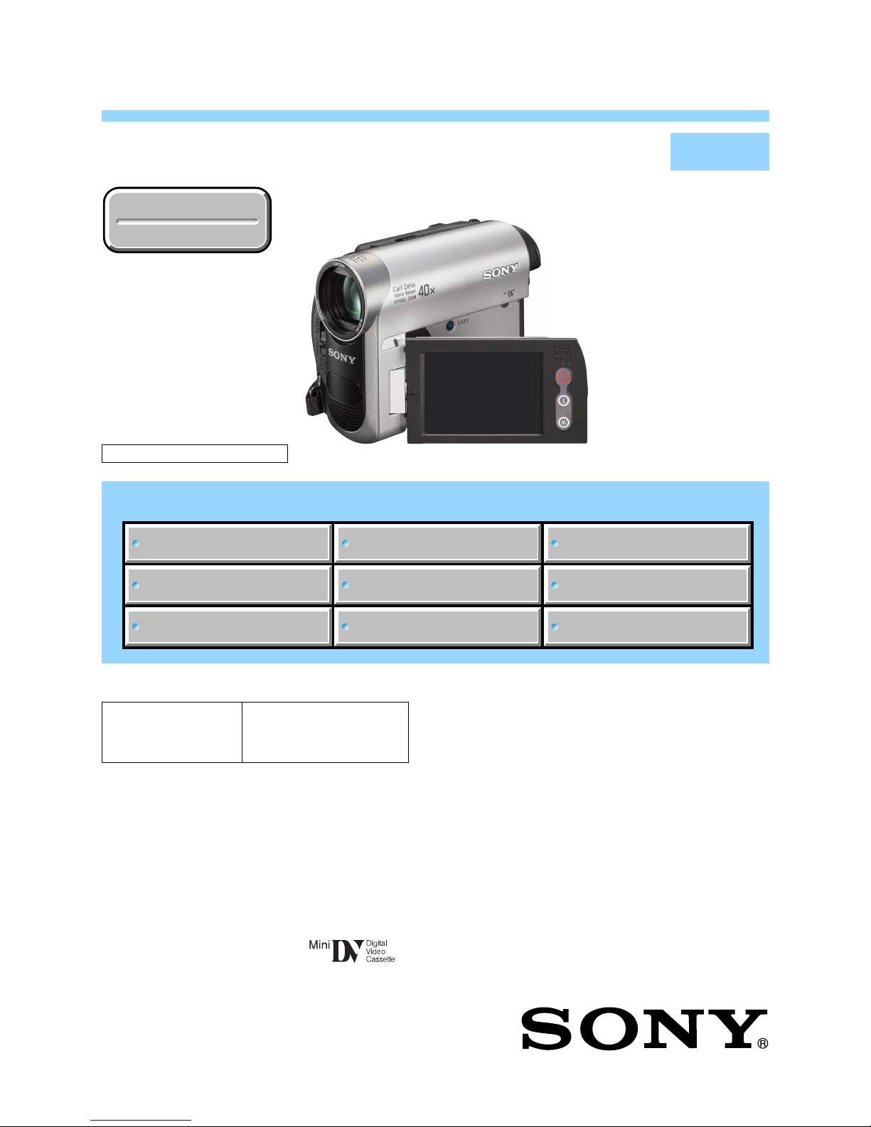
Photo: DCR-HC52
The components identified by
mark 0 or dotted line with
mark 0 are critical for safety.
Replace only with part number specified.
Les composants identifiés par une
marque 0 sont critiques pour la
sécurité.
Ne les remplacer que par une pièce
portant le numéro spécifié.
• Precaution on Replacing the VC-537 Board
N MECHANISM (MDX-N220)
US Model
Canadian Model
AEP Model
UK Model
East European Model
North European Model
E Model
Argentine Model
Australian Model
Chinese Model
Korea Model
Brazillian Model
Mexican Model
Thai Model
DCR-HC51E/HC52/HC52E/HC53E/
HC54/HC54E

— 2 —
DCR-HC51E/HC52/HC52E/HC53E/HC54/HC54E_L2
SPECIFICATIONS
These specifications are extracted from instruction
manual of DCR-HC51E/HC52E/HC53E/HC54E.
System
Video recording system
2 rotary heads, Helical scanning system
Audio recording system
Rotary heads, PCM system
Quantization: 12 bits (Fs 32 kHz, stereo
1, stereo 2), 16 bits (Fs 48 kHz, stereo)
Video signal
PAL color, CCIR standards
Usable cassette
Mini DV cassette with the mark
printed
Tape speed
SP: Approx. 18.81 mm/s
LP: Approx. 12.56 mm/s
Recording/playback time
SP: 60 min (using a DVM60 cassette)
LP: 90 min (using a DVM60 cassette)
Fast forward/rewind time
Approx. 2 min 40 s (using a DVM60
cassette and rechargeable battery pack)
Approx. 1 min 45 s (using a DVM60
cassette and AC Adaptor)
Viewfinder
Electric viewfinder (color)
Image device
3.0 mm (1/6 type) CCD (Charge
Coupled Device)
Gross: Approx. 800 000 pixels
Effective (movie): Approx. 400 000
pixels
Lens
Carl Zeiss Vario-Tessar
40
× (Optical), 2 000 × (Digital)
Focal length
f=1.9 ~ 76 mm (3/32 ~ 3 in.)
When converted to a 35 mm still
camera
In CAMERA: 36 ~ 1 440 mm (1 7/16 ~
56 3/4 in.)
F1.8 ~ 4.1
Filter diameter: 30 mm (1 3/16 in.)
Color temperature
[AUTO], [ONE PUSH], [INDOOR]
(3 200 K), [OUTDOOR] (5 800 K)
Minimum illumination
11 lx (lux) (F 1.8)
0 lx (lux) (during NightShot plus
function)
General
Power requirements
DC 6.8 V/7.2 V (battery pack)
DC 8.4 V (AC Adaptor)
Average power consumption
During camera recording using the
viewfinder 1.8 W
During camera recording using the
LCD 2.1 W
Operating temperature
0 ˚C to 40 ˚ C (32 ˚F to 104 ˚F)
Storage temperature
-20 ˚C to + 60 ˚C (-4 ˚F to + 140 ˚F)
Dimensions (approx.)
63
× 85 × 114 mm
(2 1/2
× 33/8 × 4 1/2 in.) (w/h/d)
including the projecting parts
63
× 85 × 115 mm
(2 1/2
× 33/8 × 4 5/8 in.) (w/h/d)
including the projecting parts with
supplied battery pack NP-FH30
attached
Mass (approx.)
380g(13oz) main unit only
440g(15oz) including the NP-FH30
rechargeable battery pack and DVM60
cassette.
Supplied accessories
AC Adaptor AC-L200/L200B
Power requirements
AC 100 V - 240 V, 50/60 Hz
Current consumption
0.35 - 0.18 A
Power consumption
18 W
Output voltage
DC 8.4 V*
Operating temperature
0 ˚C to 40 ˚ C (32 ˚F to 104 ˚F)
Storage temperature
-20 ˚C to + 60 ˚C (-4 ˚F to + 140 ˚F)
Dimensions (approx.)
48
× 29 × 81 mm (1 15/16 × 13/16 ×
31/4 in.) (w/h/d) excluding the
projecting parts
Mass (approx.)
170 g (6.0 oz) exclud ing the power cord
(mains lead)
*
See the label on the AC Adap tor for
other specifications.
Rechargeable battery pack (NP-FH30)
Maximum output voltage
DC 8.4 V
Output voltage
DC 7.2 V
Capacity
3.6 Wh (500 mAh)
Dimensions (approx.)
31.8
× 18.5 × 45.0 mm
(1 5/16
× 3/4 × 1 13/16 in) (w/h/d)
Mass (approx.)
40 g (1.5 oz)
Operating temperature
0 ˚C to 40 ˚C (32 ˚F to 104 ˚ F)
Type
Lithium ion
Design and specifications are subject to change
without notice.
Input/Output connectors
A/V Remote Connector
10-pin connector
Video signal: 1 Vp-p, 75
Ω (ohms)
Luminance signal: 1 Vp-p, 75
Ω (ohms)
Chrominance signal: 0.3 Vp-p, 75
Ω
(ohms)
Audio signal: 327 mV (at load
impedance 47 k
Ω (kilohms)), Output
impedance with less than 2.2 k
Ω
(kilohms)
USB jack (DCR-HC53E/HC54E)
mini-B
DV input/output jack (DCR-HC52E/
HC54E)
i.LINK Interface (IEEE1394, 4-pin
connector S100)
DV output jack (DCR-HC51E/HC53E)
i.LINK Interface (IEEE1394, 4-pin
connector S100)
LCD screen
Picture
6.2 cm (2.5 type)
Total dot number
123 200 (560
× 220)
AC Adaptor (1)
Power c ord (Mains lead) (1)
A/V connec ting c able (1 )
USB cable (1)
(DCR-HC53E/HC54E)
Rec harge able ba ttery pac k NP-FH30 (1)
CD-ROM “Ha ndycam Application
Software ” (1) (DCR-HC53E/54E )
Operating Gu ide (1)

— 3 —
DCR-HC51E/HC52/HC52E/HC53E/HC54/HC54E_L2
SPECIFICATIONS
These specifications are extracted from instruction
manual of DCR-HC52/HC54.
System
Video recording system
2 rotary heads, Helical scanning system
Audio recording system
Rotary heads, PCM system
Quantization: 12 bits (Fs 32 kHz, stereo
1, stereo 2), 16 bits (Fs 48 kHz, stereo)
Video signal
NTSC color, EIA standards
Usable cassette
Mini DV cassette with the mark
printed
Tape speed
SP: Approx. 18.81 mm/s
LP: Approx. 12.56 mm/s
Recording/playback time
SP: 60 min (using a DVM60 cassette)
LP: 90 min (using a DVM60 cassette)
Fast forward/rewind time
Approx. 2 min 40 s (using a DVM60
cassette and rechargeable battery pack)
Approx. 1 min 45 s (using a DVM60
cassette and AC Adaptor)
Viewfinder
Electric viewfinder (color)
Image device
3.0 mm (1/6 type) CCD (Charge
Coupled Device)
Gross: Approx. 680 000 pixels
Effective (movie): Approx. 340 000
pixels
Lens
Carl Zeiss Vario-Tessar
40
× (Optical), 2 000 × (Digital)
Focal length
f=1.9 ~ 76 mm (3/32 ~ 3 in.)
When converted to a 35 mm still
camera
In CAMERA: 36 ~ 1 440 mm (1 7/16 ~
56 3/4 in.)
F1.8 ~ 4.1
Filter diameter: 30 mm (1 3/16 in.)
Input/Output connectors
A/V Remote Connector
10-pin connector
Video signal: 1 Vp-p, 75
Ω (ohms)
Luminance signal: 1 Vp-p, 75
Ω (ohms)
Chrominance signal: 0.286 Vp-p, 75
Ω
(ohms)
Audio signal: 327 mV (at load
impedance 47 k
Ω (kilohms)), Output
impedance with less than 2.2 k
Ω
(kilohms)
USB jack (DCR-HC54)
mini-B
DV input/output jack
i.LINK Interface (IEEE1394, 4-pin
connector S100)
LCD screen
Picture
6.2 cm (2.5 type)
Total dot number
123 200 (560
× 2 20)
General
Power requirements
DC 6.8 V/7.2 V (battery pack)
DC 8.4 V (AC Adaptor)
Average power consumption
During camera recording using the
viewfinder 1.8 W
During camera recording using the
LCD 2.1 W
Operating temperature
0 ˚C to 40 ˚C (32 ˚F to 104 ˚ F)
AC Adaptor AC-L200/L200B
Power requirements
AC 100 V - 240 V, 50/60 Hz
Current consumption
0.35 - 0.18 A
Power consumption
18 W
Output voltage
DC 8.4 V*
Operating temperature
0 ˚C to 40 ˚ C (32 ˚F to 104 ˚F)
Storage temperature
-20 ˚C to + 60 ˚C (-4 ˚F to + 140 ˚F)
Dimensions (approx.)
48
× 29 × 81 m m (1 15/16 × 13/16 ×
31/4 in.) (w/h/d) excluding the
projecting parts
Mass (approx.)
170 g (6.0 oz) excludi ng the power cord
(mains lead)
*
See the label on the AC Adaptor for
other specifications.
Rechargeable battery pack (NP-FH30)
Maximum output voltage
DC 8.4 V
Output voltage
DC 7.2 V
Capacity
3.6 Wh (500 mAh)
Dimensions (approx.)
31.8
× 18.5 × 45.0 mm
(1 5/16
× 3/4 × 1 13/16 in) (w/h/d)
Mass (approx.)
40 g (1.5 oz)
Operating temperature
0 ˚C to 40 ˚C (32 ˚ F to 104 ˚F)
Type
Lithium ion
Design and specifications are subject to change
without notice.
Color temperature
[AUTO], [ONE PUSH], [INDOOR]
(3 200 K), [OUTDOOR] (5 800 K)
Minimum illumination
11 lx (lux) (F 1.8)
0 lx (lux) (during NightShot plus
function)
Storage temperature
-20 ˚C to + 60 ˚C (-4 ˚F to + 140 ˚F)
Dimensions (approx.)
63
× 85 × 114 mm
(2 1/2
× 33/8 × 4 1/2 in.) (w/h/d)
including the projecting parts
63
× 85 × 115 mm
(2 1/2
× 33/8 × 4 5/8 in.) (w/h/d)
including the projecting parts with
supplied battery pack NP-FH30
attached
Mass (approx.)
380g(13oz) main unit only
440g(15oz) including the NP-FH30
rechargeable battery pack and DVM60
cassette.
Supplied accessories
AC Adaptor (1)
Power c ord (Mains lead) (1)
A/V connec ting c able (1 )
USB cable (1)
(DCR-HC54)
Rec harge able ba ttery pac k NP-FH30 (1)
CD-ROM “Ha ndycam Application
Software ” (1) (DCR-HC54)
Operating Gu ide (1)

— 4 —
DCR-HC51E/HC52/HC52E/HC53E/HC54/HC54E_L2
•Abbreviation
AR : Argentine model
AUS: Australian model
BR : Brazilian model
CH : Chinese model
CND : Canadian model
EE : East European model
KR : Korea model
MX : Mexican model
NE : North European model
Model information table
HC51E
AEP, UK, NE, EE
PAL
OUT
Model
Destination
Color system
DV i.LINK Interface
USB jack
HC53E
AEP, UK, NE, EE
PAL
OUT
HC52
NTSC
IN/OUT
HC52E
NE, AUS, CH, E
US, CND, MX, BR,
AR, KR, E
PAL
IN/OUT
HC54
CND, AR, E
NTSC
IN/OUT
HC54E
NE, CH, E
PAL
IN/OUT

— 5 —
DCR-HC51E/HC52/HC52E/HC53E/HC54/HC54E_L2
SAFETY-RELATED COMPONENT WARNING!!
COMPONENTS IDENTIFIED BY MARK 0 OR DOTTED LINE WITH
MARK 0 ON THE SCHEMATIC DIAGRAMS AND IN THE PARTS
LIST ARE CRITICAL TO SAFE OPERATION. REPLACE THESE
COMPONENTS WITH SONY PARTS WHOSE PART NUMBERS
APPEAR AS SHOWN IN THIS MANUAL OR IN SUPPLEMENTS
PUBLISHED BY SONY.
1. Check the area of your repair for unsoldered or poorly-soldered
connections. Check the entire board surface for solder splashes
and bridges.
2. Check the interboard wiring to ensure that no wires are
"pinched" or contact high-wattage resistors.
3. Look for unauthorized replacement parts, particularly
transistors, that were installed during a previous repair. Point
them out to the customer and recommend their replacement.
4. Look for parts which, through functioning, show obvious signs
of deterioration. Point them out to the customer and
recommend their replacement.
5. Check the B+ voltage to see it is at the values specified.
6. Flexible Circuit Board Repairing
•Keep the temperature of the soldering iron around 270˚C
during repairing.
• Do not touch the soldering iron on the same conductor of the
circuit board (within 3 times).
• Be careful not to apply force on the conductor when soldering
or unsoldering.
SAFETY CHECK-OUT
After correcting the original service problem, perform the following
safety checks before releasing the set to the customer.
ATTENTION AU COMPOSANT AYANT RAPPORT
À LA SÉCURITÉ!
LES COMPOSANTS IDENTIFÉS PAR UNE MARQUE 0 SUR LES
DIAGRAMMES SCHÉMATIQUES ET LA LISTE DES PIÈCES SONT
CRITIQUES POUR LA SÉCURITÉ DE FONCTIONNEMENT. NE
REMPLACER CES COMPOSANTS QUE PAR DES PIÈSES SONY
DONT LES NUMÉROS SONT DONNÉS DANS CE MANUEL OU
DANS LES SUPPÉMENTS PUBLIÉS PAR SONY.
Unleaded solder
Boards requiring use of unleaded solder are printed with the leadfree mark (LF) indicating the solder contains no lead.
(Caution: Some printed circuit boards may not come printed with
the lead free mark due to their particular size.)
: LEAD FREE MARK
Unleaded solder has the following characteristics.
• Unleaded solder melts at a temperature about 40°C higher than
ordinary solder.
Ordinary soldering irons can be used but the iron tip has to be
applied to the solder joint for a slightly longer time.
Soldering irons using a temperature regulator should be set to
about 350°C.
Caution: The printed pattern (copper foil) may peel away if the
heated tip is applied for too long, so be careful!
• Strong viscosity
Unleaded solder is more viscous (sticky, less prone to flow) than
ordinary solder so use caution not to let solder bridges occur such
as on IC pins, etc.
•Usable with ordinary solder
It is best to use only unleaded solder but unleaded solder may
also be added to ordinary solder.
CAUTION
Danger of explosion if battery is incorrectly replaced.
Replace only with the same or equivalent type.
1-1
DCR-HC51E/HC52/HC52E/HC53E/HC54/HC54E_L2
1. SERVICE NOTE
1-1. POWER SUPPLY DURING REPAIRS
In this unit, about 10 seconds after power is supplied to the battery terminal using the regulated power supply (8.4V), the power is shut off so
that the unit cannot operate.
These following method is available to prevent this.
Method:
Use the AC power adaptor (AC-L200/L200B).
1-2. TO TAKE OUT A CASSETTE WHEN NOT EJECT (FORCE EJECT)
1 Refer to “2. DISASSEMBLY” to remove the mechanism deck block.
2 Supply +4.5V from the DC power supply to the loading motor and unload with a pressing the cassette compartment.
Loading motor
DC power suppl
y
(+ 4.5Vdc)
1-3. SETTING THE “FORCED POWER ON” MODE
It is possible to turn on power by adjustment remote commander (RM-95 or NEW LANC JIG).
Operate the VTR function using the adjustment remote commander.
1-3-1. Setting the “Forced Camera Power ON” Mode
1) Select page: 0, address: 01, and set data:01.
2) Select page: A, address: 10, set data:01 and press the “PAUSE (Write)” button of the adjustment remote commander.
1-3-2. Setting the “Forced VTR Power ON” Mode
1) Select page: 0, address: 01, and set data:01.
2) Select page: A, address: 10, set data:02 and press the “PAUSE (Write)” button of the adjustment remote commander.
1-3-3. Exiting the “Forced Power ON” Mode
1) Select page: 0, address: 01, and set data:01.
2) Select page: A, address: 10, set data:00 and press the “PAUSE (Write)” button of the adjustment remote commander.
3) Select page: 0, address: 01, and set data: 00.
1-2
DCR-HC51E/HC52/HC52E/HC53E/HC54/HC54E_L2
1-5. SELF-DIAGNOSIS FUNCTION
1-5-1. Self-diagnosis Function
When problems occur while the unit is operating, the self-diagnosis
function starts working, and displays on the viewfinder or LCD
screen what to do.
Details of the self-diagnosis functions are provided in the Instruction
manual.
1-5-2. Self-diagnosis Display
When problems occur while the unit is operating, the counter of the
viewfinder or LCD screen shows a 4-digit display consisting of an
alphabet and numbers, which blinks at 3.2 Hz. This 5-character
display indicates the “repaired by:”, “block” in which the problem
occurred, and “detailed code” of the problem.
1 1
3 1C
Repaired by:
Refer to “1-5-3. Self-diagnosis Code Table”.
Indicates the appropriate
step to be taken.
E.g.
31 ....Reload the tape.
32 ....Turn on power again.
Block
Detailed Code
Blinks at 3.2Hz
C : Corrected by customer
H : Corrected by dealer
E : Corrected by service
engineer
Viewfinder or LCD screen
C : 3 1 : 1 1
18
CN1014
VC-537 BOARD
(SIDE A)
1
8
CPC-15
(J-6082-564-A)
I/F unit for LANC control
(J-6082-521-A)
1-4. USING SERVICE JIG
Connect the CPC-15 jig connector (J-6082-564-A) and I/F unit for LANC control (J-6082-521-A) to the CN1014 of VC-537 board.
1-3
DCR-HC51E/HC52/HC52E/HC53E/HC54/HC54E_L2
1-5-3. Self-diagnosis Code Table
C
C
C
C
C
C
C
C
C
C
C
C
C
C
C
C
C
C
C
C
C
C
C
C
C
C
C
C
C
Block
Function
04
21
22
31
31
31
31
31
31
31
31
31
31
31
31
31
32
32
32
32
32
32
32
32
32
32
32
32
32
Detailed
Code
00
00
00
10
11
20
21
22
23
30
31
40
41
42
43
44
10
11
20
21
22
23
30
31
40
41
42
43
44
Symptom/State
Non-standard battery is used.
Condensation.
Video head is dirty.
LOAD direction. Loading does not
complete within specified time
UNLOAD direction. Loading does not
complete within specified time
T reel side tape slacking when unloading
.
S reel
side tape slacking when unloading
.
T reel fault.
S reel fault.
FG fault when starting capstan.
FG fault during normal capstan operations.
FG fault when starting drum.
PG fault when starting drum.
FG fault during normal drum operations.
PG fault during normal drum operations.
Phase fault during normal drum operations.
LOAD direction loading motor timeout.
UNLOAD direction loading motor
time-out.
T reel side tape slacking when
unloading.
S reel side tape slacking when
unloading.
T reel fault.
S reel fault.
FG fault when starting capstan.
FG fault during normal capstan
operations.
FG fault when starting drum.
PG fault when starting drum.
FG fault during normal drum
operations.
PG fault during normal drum
operations.
Phase fault during normal drum
operations.
Repaired by:
Correction
Use the InfoLITHIUM battery.
Remove the cassette, and insert it again after one hour.
Clean with the optional cleaning cassette.
Load the tape again, and perform operations from the beginning.
Load the tape again, and perform operations from the beginning.
Load the tape again, and perform operations from the beginning.
Load the tape again, and perform operations from the beginning.
Load the tape again, and perform operations from the beginning.
Load the tape again, and perform operations from the beginning.
Load the tape again, and perform operations from the beginning.
Load the tape again, and perform operations from the beginning.
Load the tape again, and perform operations from the beginning.
Load the tape again, and perform operations from the beginning.
Load the tape again, and perform operations from the beginning.
Load the tape again, and perform operations from the beginning.
Load the tape again, and perform operations from the beginning.
Remove the battery or power cable, connect, and perform
operations from the beginning.
Remove the battery or power cable, connect, and perform
operations from the beginning.
Remove the battery or power cable, connect, and perform
operations from the beginning.
Remove the battery or power cable, connect, and perform
operations from the beginning.
Remove the battery or power cable, connect, and perform
operations from the beginning.
Remove the battery or power cable, connect, and perform
operations from the beginning.
Remove the battery or power cable, connect, and perform
operations from the beginning.
Remove the battery or power cable, connect, and perform
operations from the beginning.
Remove the battery or power cable, connect, and perform
operations from the beginning.
Remove the battery or power cable, connect, and perform
operations from the beginning.
Remove the battery or power cable, connect, and perform
operations from the beginning.
Remove the battery or power cable, connect, and perform
operations from the beginning.
Remove the battery or power cable, connect, and perform
operations from the beginning.
Self-diagnosis Code
1-4E
DCR-HC51E/HC52/HC52E/HC53E/HC54/HC54E_L2
E
E
E
Block
Function
61
61
61
Detailed
Code
00
10
11
Symptom/State
Difficult to adjust focus
(Cannot initialize focus.)
Zoom operations fault
(Cannot initialize zoom lens.)
Focus lens initializing failure and zoom
lens initializing failure occur simultaneously.
Self-diagnosis Code
Repaired by:
Correction
Inspect the lens block focus reset sensor (Pin 7, of CN3101 of VC537 board) when focusing is performed when the touch panel is
operated in the focus manual mode and the focus motor drive circuit
(IC3101 of VC-537 board) when the focusing is not performed.
Inspect the lens block zoom reset sensor (Pin qa, of CN3101 of
VC-537 board) when zooming is performed when the zoom switch
is operated and the zoom motor drive circuit (IC3101 of VC-537
board) when zooming is not performed.
Inspect the flexible board for breakage or loose connection.
If not faulty, inspect the focus and zoom motor drive circuit (IC3101
of VC-537 board).
1-6. PRECAUTION ON REPLACING THE VC-537 BOARD
Exif Model Data Check
When you replace to the repairing board, the written data of repairing board also might be changed to original setting.
When the data has changed because of board replaceing etc, check the data setting (Exif Model Data) is right. If not, rewrite to the right value.
Exif Model Data
Page
C
C
C
Data
DCR-HC51E
35
31
45
DCR-HC52
35
32
00
Address
D2
D3
D4
DCR-HC52E
35
32
45
DCR-HC53E
35
33
45
DCR-HC54
35
34
00
DCR-HC54E
35
34
45
Writing Method:
1) Select page: 0, address: 01 and set data: 01.
2) Select page: C, address: D2 to D4, and set the Exif Model Data.
Note: To write in the non-volatile memory (EEPROM), press the PAUSE (Write) button each time to set the data.
3) Select page: 0, address: 01, and set data: 00.
2-1
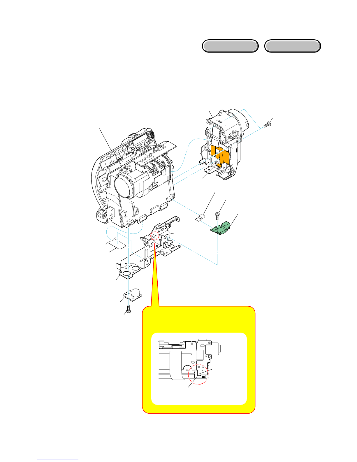
2. DISASSEMBLY
DCR-HC51E/HC52/HC52E/HC53E/HC54/HC54E_L2
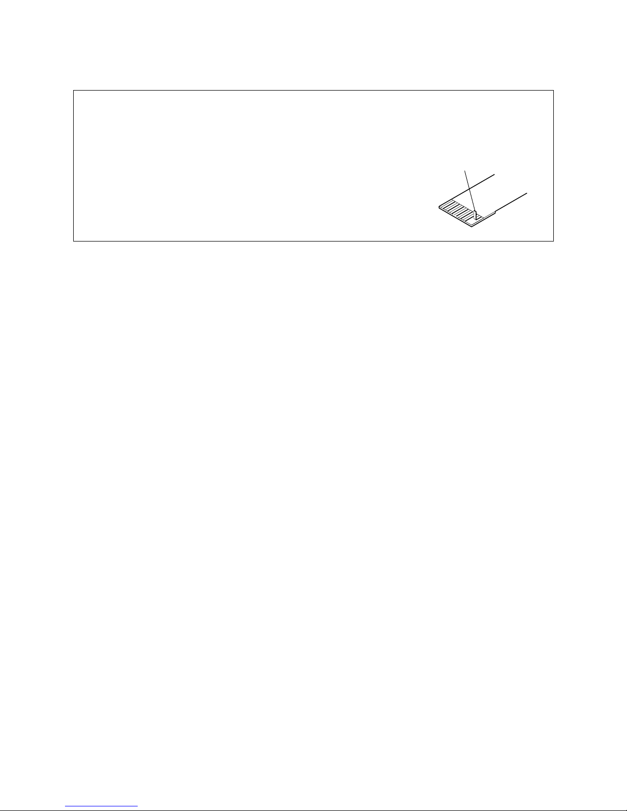
NOTE FOR REPAIR
• Make sure that the flat cable and flexible board are not cracked of bent at the terminal.
Do not insert the cable insufficiently nor crookedly.
• When remove a connector, don’t pull at wire of connector. It is possible that a wire is snapped.
• When installing a connector, don’t press down at wire of connector.
It is possible that a wire is snapped.
Cut and remove the part of gilt
which comes off at the point.
(Be careful or some
pieces of gilt may be left inside)
2-2
DCR-HC51E/HC52/HC52E/HC53E/HC54/HC54E_L2
2-1. IDENTIFYING PARTS
2-2-1. OVERALL SECTION
- Front Cabinet Block
- Microphome Unit
- Cabinet (L)
- Cabinet (Upper (2122))
2-2-2. BOTTOM FRAME SECTION
- JK-367 Board
- Bottom Frame
- BT-EVF Section
2-2-3. CABINT (L) SECTION
- VC-537 Board
- CD-735 Board
- Lens Device LSV-1171A
- Mechanism Deck
- Control Key Block (SS21200)
2-2-4. CABINET (R) SECTION
- Loud Speaker
- CF-111 Board
- LCD Panel Block
BT-EVF Section
⋅ LB-137 Board
⋅
AV-125 Board
⋅
FP-626 Flexible Board
Cabinet (L) Section
⋅ VC-537 Board
⋅
CD-735 Board
Cabinet (R) Section
⋅ CF-111 Board
⋅
PD-358 Board
⋅
FP-386 Flexible Board
⋅
FP-625 Flexible Board
Front Cabinet Block
Bottom Frame
- DISASSEMBLY FLOW -
Cabinet (Upper (2122))
Cabinet (L)
JK-367 Board
2-3
DCR-HC51E/HC52/HC52E/HC53E/HC54/HC54E_L2
2-2. DISASSEMBLY
2-2-1. OVERALL SECTION
Follow the disassembly in the numerical order given.
1 Cabinet (R) Section (1-1 to 1-14)
2 Front Cabinet Block (2-1 to 2-6)
HELP
HELP
EXPLODED VIEW
HARDWARE LIST
1 Cabinet (R)
Section
(See Page 2-6)
1-1
(Open)
1-2 (#2)
1-3
1-4
1-5
2-1 (#2)
2-3
2-4 (#1)
2-5 (#1)
2-6
2-2 (#2)
Note: On installation of the NS knob,
adjust the position of the NS
switch and the NS knob.
1-12
(Boss)
1-11
(Boss)
1-6
(#2)
1-7
(#2)
1-14
1-13
1-9
(#2)
1-8
(Open)
2 Front Cabinet
Block
1-10
(Claw)
Bottom Frame
Section
(See Page 2-4)
2-4
DCR-HC51E/HC52/HC52E/HC53E/HC54/HC54E_L2
2-2-2. BOTTOM FRAME SECTION
Follow the disassembly in the numerical order given.
1 BT-EVF Section (1-1 to 1-3)
2 JK-367 Board (2-1 to 2-7)
EXPLODED VIEW
HARDWARE LIST
Cabinet (L) Section
(See Page 2-5)
1 BT-EVF Section
1-2
1-3
1-1 (#2)
2-4
2-6
2-2
2-3 (#1)
2-1
2-5 (Claw)
2 JK-367 Board
2-7 (#3)
Note:On installation of the bottom frame,
insert the claw of the bottom frame
to the hole of the MD frame.
Claw
(Bottom Frame)
Hole
(MD Frame)
2-5
DCR-HC51E/HC52/HC52E/HC53E/HC54/HC54E_L2
2-2-3. CABINET (L) SECTION
Follow the disassembly in the numerical order given.
1 Lens Block (1-1 to 1-3)
2 VC-537 Board (2-1 to 2-8)
3 Mechanism Deck (3-1 to 3-3)
EXPLODED VIEW
HARDWARE LIST
2 VC-537
Board
3 Mechanism Deck
1-1
1-3
1-2 (#12)
2-1
2-2
2-8
2-3
2-7
3-3 (#15)
3-2
2-4 (#3)
2-5 (Claw)
3-1 (Claw)
VC-537
2-6
(Claw)
1 Lens Block
HELP01
2-6E
DCR-HC51E/HC52/HC52E/HC53E/HC54/HC54E_L2
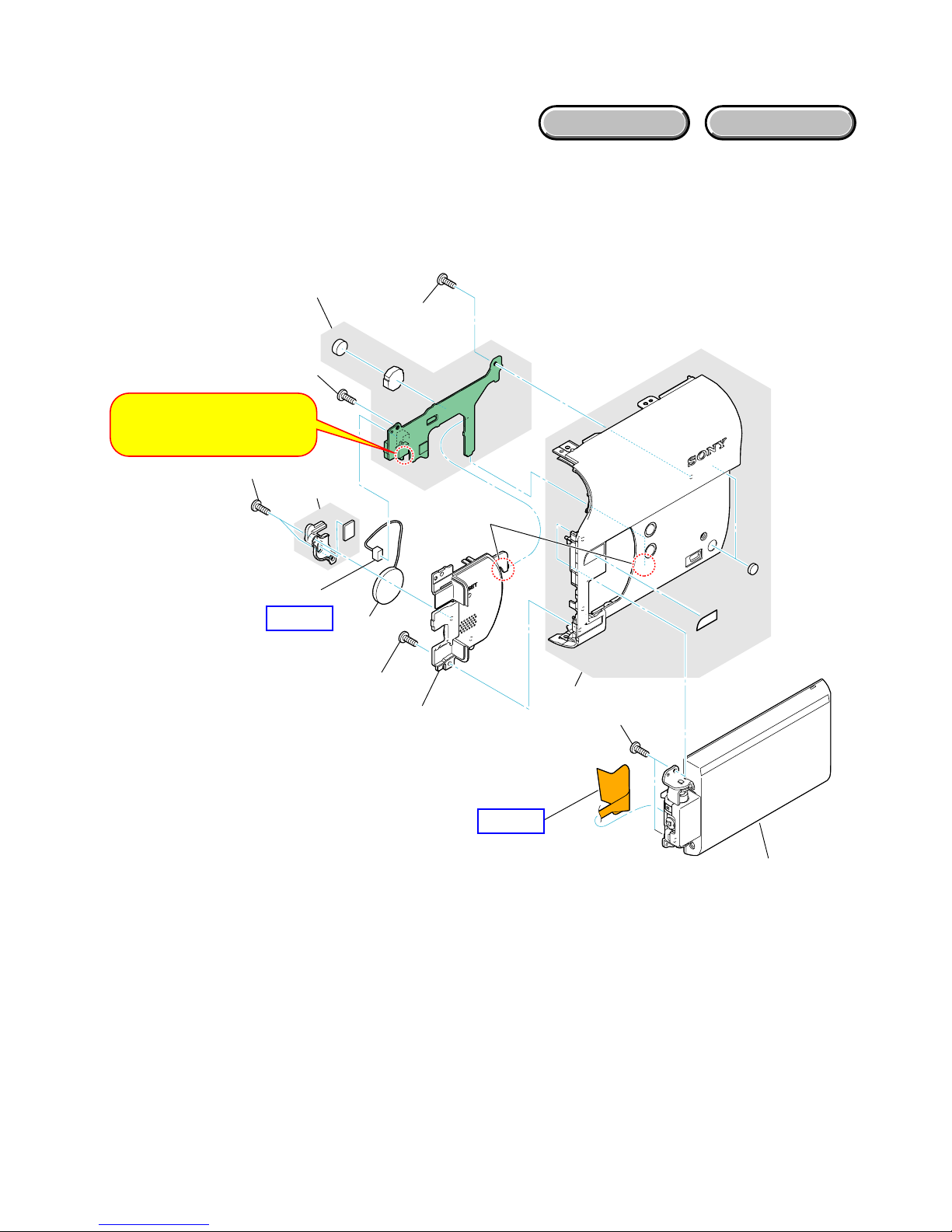
2-2-4. CABINET (R) SECTION
Follow the disassembly in the numerical order given.
1 CF-111 Board (1-1 to 1-7)
2 LCD Panel Block (2-1 to 2-4)
EXPLODED VIEW
HARDWARE LIST
1 CF-111 Board
1-1
1-4
1-5 (#12)
2-2
2-1 (#12)
2-3 (#12)
1-7
(Claw)
2 LCD Panel
Block
1-2 (#12)
1-6 (#12)
Note:On installation of the CF-111
board, adjust the position of
the Panel Open/Close switch.
1-3
2-4
HELP02
HELP03
HELP
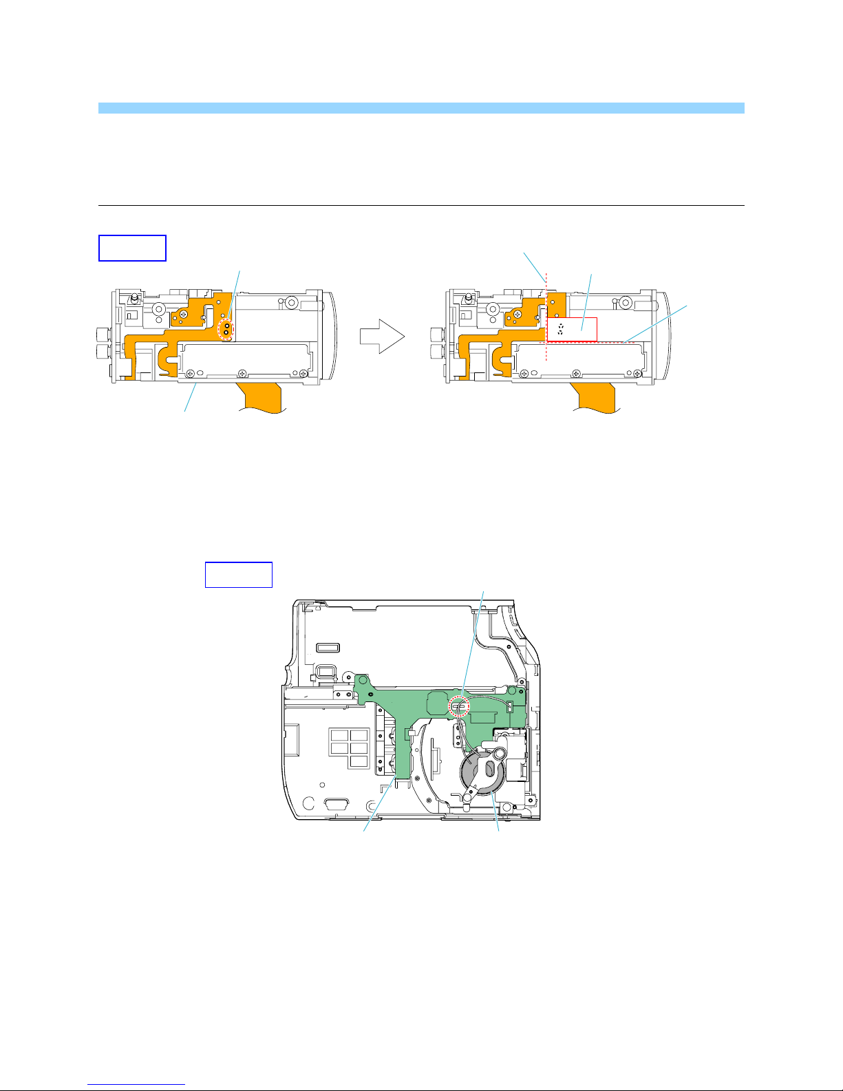
DCR-HC51E/HC52/HC52E/HC53E/HC54/HC54E_L2
HELP
Sheet attachment positions and procedures of processing the flexible boards/harnesses are shown.
Harness arrangement
Plating Lead
Lens Device
(LSV-1171A)
Loud SpeakerCF-111 Board
F Insulating Sheet
Sticking Standard
Sticking
Standard
HELP01
HELP02
HELP
DCR-HC51E/HC52/HC52E/HC53E/HC54/HC54E_L2
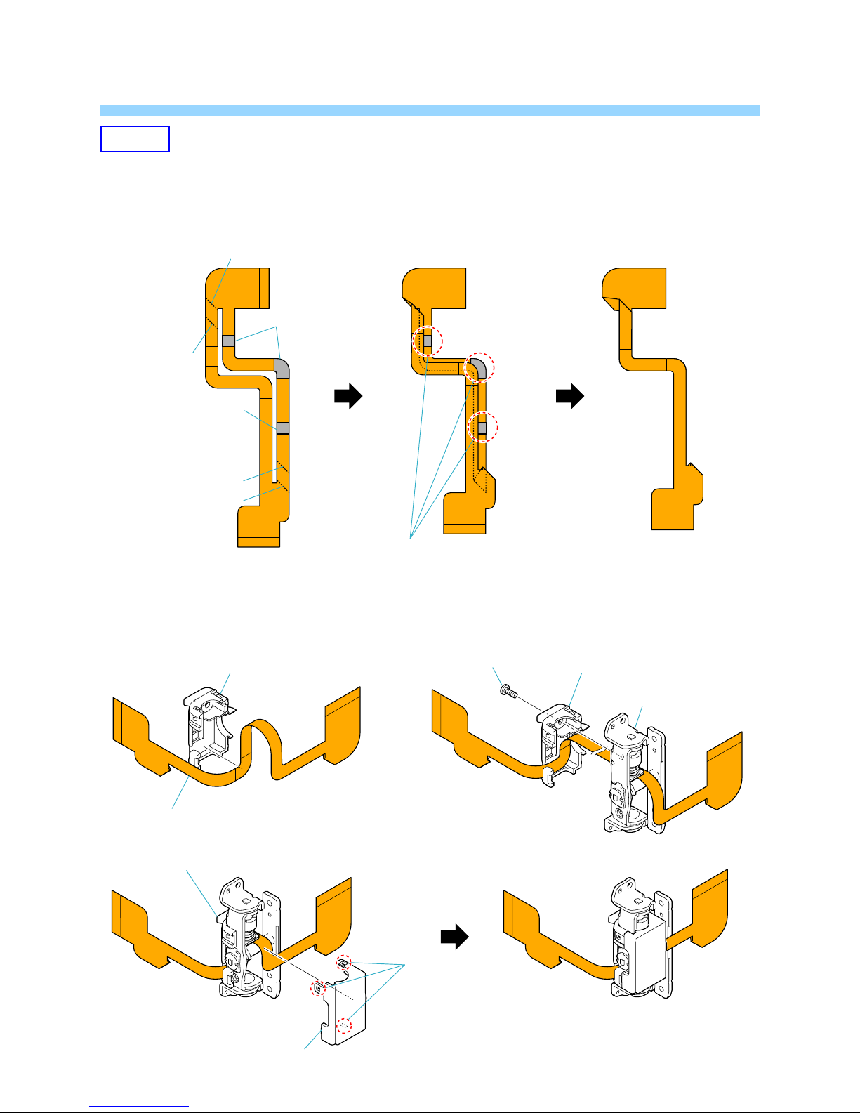
4 Install the hinge cover (C) in the hinge cover (M).
Hinge cover (M)
Hinge cover (C)
Claw
Panel hinge assy (M)
2 Put the FP-625 flexible board on the
hinge cover (M).
3 Fix hinge cover (M) and the panel hinge assy (M)
with the screw.
Screw
Hinge cover (M)
FP-625 flexible board
Hinge cover (M)
1 Fold dotted line parts of the FP-625 flexible board
as shown in figure.
Valley fold
Mountain
fold
Stick it together in the adhesive tape
while bending the FP-625 flexible board.
Mountain
fold
Valley fold
Adhesive tape
Adhesive tape
THE METHOD OF ATTACHMENT OF FP-625 FLEXIBLE BOARD
HELP03
DCR-HC51E/HC52/HC52E/HC53E/HC54/HC54E_L2
Link
Link
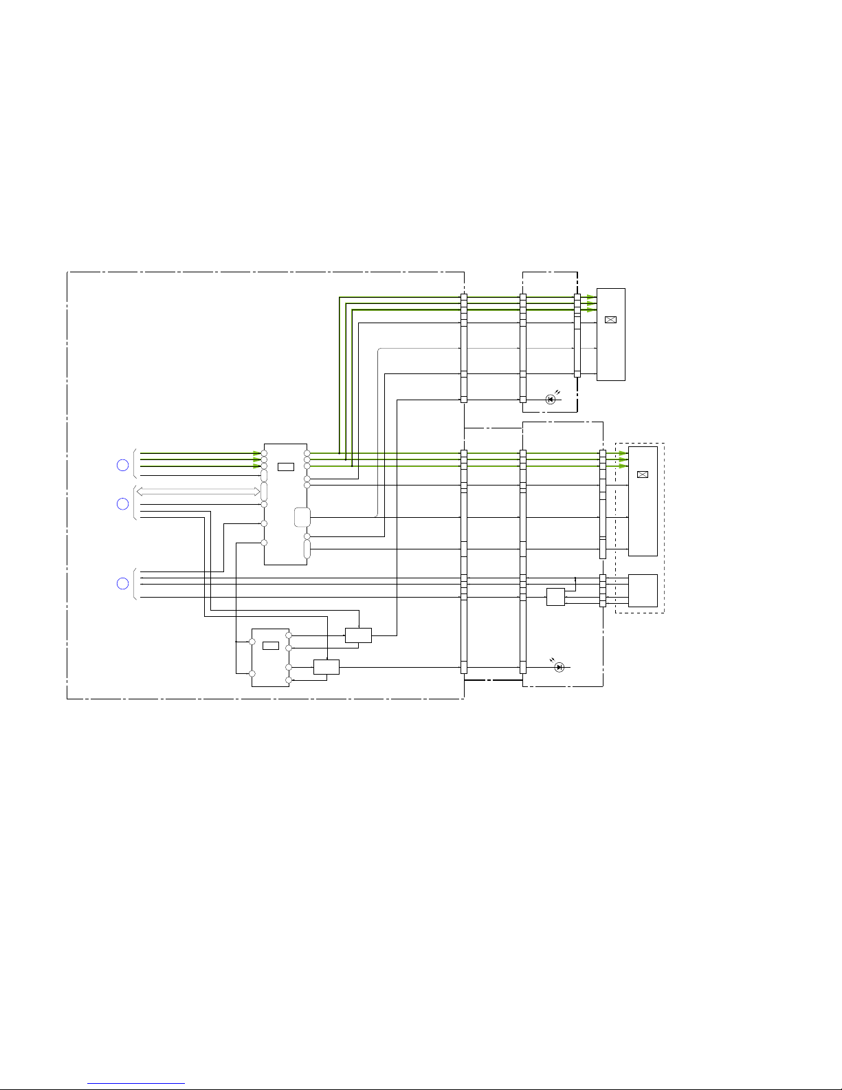
3. BLOCK DIAGRAMS
OVERALL BLOCK DIAGRAM (4/5)
OVERALL BLOCK DIAGRAM (3/5)
OVERALL BLOCK DIAGRAM (2/5)
OVERALL BLOCK DIAGRAM (1/5)
POWER BLOCK DIAGRAM (3/3)
POWER BLOCK DIAGRAM (2/3)
POWER BLOCK DIAGRAM (1/3)
OVERALL BLOCK DIAGRAM (5/5)
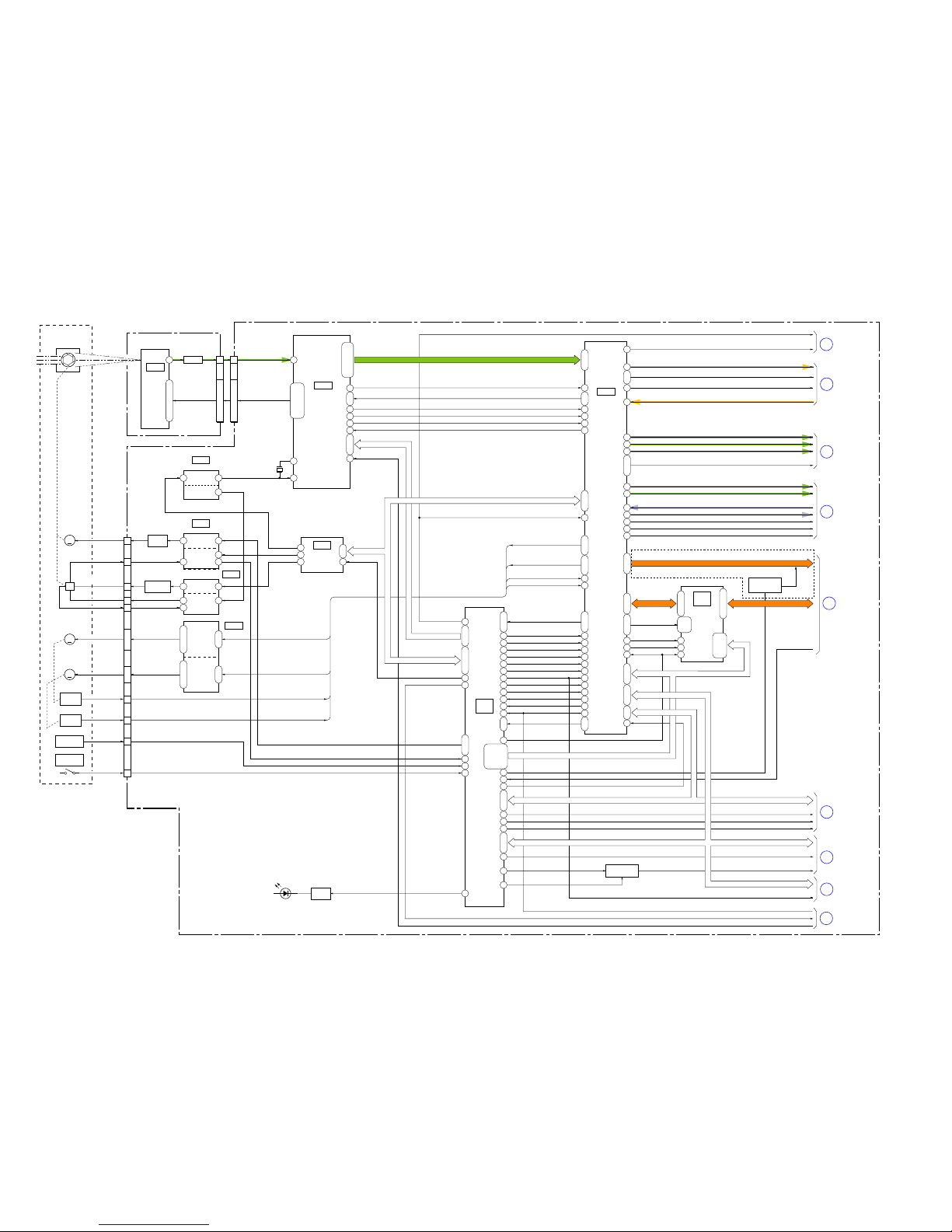
3-1
DCR-HC51E/HC52/HC52E/HC53E/HC54/HC54E_L2
3. BLOCK DIAGRAMS
3-1. OVERALL BLOCK DIAGRAM (1/5) ( ) : Number in parenthesis ( ) indicates the division number of schematic diagram where the component is located.
A10
S/H, AGC,
A/D CONVERTER,
TIMING
GENERATOR
(4/13)
IC3001
P6
N3
P2
P3
F14
N5
N2
X3001
36MHz
P5
CN7101
CD-735 BOARD
VC-537 BOARD (1/5)
V1 - V4, RG,
VSHT, H1, H2
7
CCD
IMAGER
IRIS
(SHUTTER)
H
M
IRIS
METER
M
FOCUS
SENSOR
ZOOM
SENSOR
FOCUS
MOTOR
ZOOM
MOTOR
M
LENS BLOCK
CCD_ OUT
CN3101
13
17
18
7
LENS TEMP
SENSOR
IC7101
BUFFER
Q7101
IRIS
DRIVE
Q3101
HALL GAIN
CONTROL
Q3103
LED
DRIVE
Q1001
8
NIGHTSHOT
PLUS
(5/13)
IRIS DRIVE
I_DRIVE (-)
I_BIAS (-)
15
I_BIAS (+)
I_HALL (-)
16
I_HALL (+)
FC_A, FC_XA,
FC_B, FC_XB
ZM_A, ZM_XA,
ZM_B, ZM_XB
FC_SENS_OUT
11
ZM_SENS_OUT
6
THERMO_OUT
19
NightShot_Vcc
FC_RST
ZM_RST
HALL AMP
IC3103
(5/13)
IC3102
(5/13)
IC3101
FOCUS
MOTOR
DRIVE
ZOOM
MOTOR
DRIVE
SPCK
CAMERA/
MECHA
CONTROL
(10/13)
OVERALL (5/5)
(PAGE 3-5)
9
OVERALL (2/5)
(PAGE 3-2)
1
216
214
215
212
213
190
LD_EN0, LD_DIR0A, LD_DIR0B
LD_EN1, LD_DIR1A, LD_DIR1B
FC_RST
ZM_RST
LD_EN0, LD_DIR0A, LD_DIR0B
LD_EN1, LD_DIR1A, LD_DIR1B
14
15
DV SIGNAL
PROCESS
(6/13)
IC6001
IR_ON
B6
A13
R22
P20
D17
Y18
Y5
CN3001
7
VCK
XRST_VTR
XSYS_RST
XRST_VTR
TG_AHD, TG_AVD
TG_ZSG1
TG_ZV1
TG_ID
TG_VGAT
CH_SO, CH_SCK, XCS_TG
CH_SO, CH_SCK, XCS_TG
CAM_SO, CAM_SCK
XTAL AMP
HALL REG
IC3104
(5/13)
IC9201
EVR
(D/A CONVERTER)
(12/13)
FREQ_AMPOUT
FREQ_TUNE
75
1
1
2
3
8
1
7
HALL GAIN
5 7
HALL_OFFSET
5
HALL_GAIN
6
3
HALL BIAS
1 3
2
TRCKO
143
DV INTERFACE
(6/13)
19
LCKO
XACC, XENA, DIR,
FCLR, FRL
159
62
78
177
XCS_IC_6002
XCS_OSD
XCS_IC_6002
LBUS0 - LBUS3
USB_D+, USB_D- USB_D+, USB_D-
USB_D+
USB_DET
D24A00 - D31A07, DXXA08, DXXA09, ALE, WRX, RDX
D24A00 - D31A07, DXXA08, DXXA09, ALE, WRX, RDX
78
77
96
OVERALL (2/5)
(PAGE 3-2)
2
OVERALL (4/5)
(PAGE 3-4)
4
OVERALL (3/5)
(PAGE 3-3)
3
OVERALL (4/5)
(PAGE 3-4)
5
OVERALL (3/5)
(PAGE 3-3)
6
OVERALL (4/5)
(PAGE 3-4)
7
OVERALL (2/5)
(PAGE 3-2)
8
RECDT
RECA1, RECA2
RECCK
RFIN
DATA_TO_SFD
SFD_BCK
DATA_FROM_SFD
SFD_FCK
SFD_LRCK
IC_6001_C_OUT
IC_6001_Y_OUT
63
68
64
69
67
110
113
121
123
119
141
PANEL_R
PANEL_G
PANEL_B
PANEL_HD, PANEL_VD
OSD_V
OSD_V
CAM_DD_ON
VFO_VD, VFO_OE
USB_DET
XUSB_ON
XCS_OSD
MELODY_ENV
MELODY_CARR
XUSB_EN
VREF
LINE_OUT_VD
189
XCS_IC_6001
FRRV, TRRV, TRRT
193
XCS_IC_6001_1
197
XIRQ_IC_8601
192
181
182
129
SWP
161
DRP
162
XCS_SFD
187
XCS_VFD
188
Y17
C22
D6
B3
W20
N20
B7
J2
B8
N22
A21
163
ATF_LATCH
B22
B21
E23
B2
VD_SO, VD_SCK
VD_SI, VD_SO, VD_SCK
VD_SI, VD_SO, VD_SCK
VSP_SO, XVSP_SCK
VSP_SO, XVSP_SCK
VSP_SI, VSP_SO, XVSP_SCK
VSP_SI, VSP_SO, XVSP_SCK
SWP
XSYS_RST
U1
XCS_EVF
V1
EVF_BL_ON
AB9
PANEL_BL_ON
U2
XCS_AU1
AC18
BEEP
D8
D1026
(NIGHTSHOT)
TPA+, TPA-, TPB+, TPB-
AD0 - AD9
A : VIDEO SIGNAL
A : AUDIO SIGNAL
A : VIDEO/AUDIO SIGNAL
A : VIDEO/AUDIO/SERVO SIGNAL
3 - 6, 14, 13 11,10
21 - 241 - 4
1, 2, 4, 5, 9 - 12
N1, M2
199 - 208196 - 194180 - 178
157 - 154145 - 149164 - 176184 - 186
24, 26 - 28
52, 51, 48, 47
N4, P8, P9, P11,
P12, N10, P7, N6
1 - 4, 9, 10, 12, 13
2, 23, 4, 215, 19, 17, 7
6, 7
9 - 1213 - 16
4, 311, 5, 612, 8, 9
L2, D15, A16
Y11, AB11, AB10
AA2, Y2, W4,
W2, Y1, V4,
V2, W1, P2,
P1, K4, L1, L4
Y16, AC17
42, 43
75, 76131, 130126, 127
2 - 4, 6 - 9
11, 75 - 77
12 - 15
17
A7, Y8
Q8601, Q8602
MODULATOR
A2 - A4
AC9, Y9, K1
DA_STRB
DA_STRB
HALL_AD
LENS_TEMP_AD
XNS_SW
CAM_DD_ON
CAM_SI, CAM_SO, CAM_SCK
IRIS_PWM, IRIS_COM
19
18, 20
Y12, AC12, Y13
AC8, AB8, AC7
AC5
C1, D2, D1, E2, E1,
F2, F1, G1, G2, H1
XRST_VTR
CAM_SI, CAM_SO, CAM_SCK
IC8601
(1/2)
IC6002
(1/2)
USB
PULL UP
Q6003
HC53E/HC54/HC54E
3-2
DCR-HC51E/HC52/HC52E/HC53E/HC54/HC54E_L2
3-2. OVERALL BLOCK DIAGRAM (2/5)
( ) : Number in parenthesis ( ) indicates the division number of schematic diagram where the component is located.
A : VIDEO/AUDIO/SERVO SIGNAL
A : SERVO SIGNAL
IC8601
(2/2)
VC-537 BOARD (2/5)
IC9001
(3/3)
IC2201
(1/2)
CAP_PWM
DRUM_ERROR
CAP_ERROR
DRUM
MOTOR
DRIVE
FG AMP
PG AMP
535052
49
21 20
18
MECHA
CONTROL
(10/13)
Q2208
CN1009
DRUM FG
M901
DRUM MOTOR
DRUM_VS
LOADING
MOTOR
DRIVE
TAPE END
DETECT
43
45
LPF
Q2207
10
CAPSTAN
MOTOR
DRIVE
FG AMP
4
DRUM_U, V, W
LM_
LOAD, UNLOAD
TAPE_END_C
DRUM_FG
DRUM_PG
CAP_VS
CAP_FWD, CAP_ON
CAP_FWD, CAP_ON
CAP_FG
DRUM_FG
DRUM_PG
DEW_AD
MODE_SW_A - MODE_SW_C
MODE_SW_A - MODE_SW_C
LOAD, UNLOAD
TAPE_END
TAPE_LED_ON
TAPE_END
CAP_FG
8
7
9
28
16
25
11
18
TAPE_TOP_C
TAPE TOP
DETECT
T REEL
FG AMP
S REEL
FG AMP
DEW_AD
CAP_U, V, W
CN1007
6
M
DRUM PG
M903
CAPSTAN MOTOR
M
HU, HV, HW
DEW SENSOR
MODE SWITCH
S903
Q9002
M902
LOADING MOTOR
Q901
TAPE END
SENSOR
D901
TAPE LED
M
FG1, FG2
CAPSTAN FG
Q902
TAPE TOP
SENSOR
H902
T REEL
SENSOR
H901
MIC902
S901
CC DOWN
S902
REC PROOF
S REEL
SENSOR
4PIN
CONNECTOR
(11/13)
IC9001
(1/3)
(11/13)
IC9001
(2/3)
(11/13)
DRUM/
CAPSTAN
PWM DRIVE
(3/13)
21
7
24
8
DRUM_FG_SENS
59
DRUM_COM
51
FG_PG_COM
DRUM_PG_SENS
LED
DRIVE
TAPE_LED_K
1
IC8602
EEPROM
(10/13)
D1
C1
X8601
20MHz
XCS_EEP
F1
SERIAL
INTERFACE
38, 36
77, 78
64, 67
63, 65, 6874, 76, 78
75, 771, 80
10 - 157, 8
75, 76
37
XCS_IC_9001_1
34
XRST_VTR
OVERALL (1/5)
(PAGE 3-1)
1
OVERALL (1/5)
(PAGE 3-1)
8
F2
XSYS_RST
F4
LM_LIM_DET LM_LIM_DET
41
35
SPCKSPCK
EEP_SI, EEP_SO, EEP_SCK
OVERALL (1/5)
(PAGE 3-1)
2
OVERALL (5/5)
(PAGE 3-5)
10
REC_PROOF
CHIME_SDA, CHIME_SCK
XRST_VTR
IC_8001_SI, IC_8001_SO, IC_8001_SCK, XCS_IC_8001
VIDEO HEAD
CN1008
RF_MON
ODD
XODD, YODD
XEVEN, YEVEN
SWP
CN1014
EVEN
SWP
IC6501
REC/PB AMP
(7/13)
XCS_EEP
2
4
7 - 5
1
30
44
35
46
38
CPC
(FOR CHECK)
CONT1, SW_PS, ALL_PSCONT1, SW_PS, ALL_PS
RECDT
RECA1, RECA2
RECCK
RFIN
RF_MON
N MECHANISM DECK
(MDX-N220)
VSP_SO, XVSP_SCKVSP_SO, XVSP_SCK
SWITCH
SWITCH
31
AC15
N4
B9
A9
D10, B10,
W23, V20
D19, B20
D11
V23
H4
L22
19
N2
TAPE_TOP
TAPE_TOP
29
B11
TREEL_FG
TREEL_FG
A11
25
SREEL_FG
SREEL_FG
REC_PROOF
CHIME_SDA, CHIME_SCK
XCC_DOWNXCC_DOWN
B15
B5
SWP
EEP_SI, EEP_SO, EEP_SCK
ZOOM_VR_AD
SYS_V
D14
M22
2, 5, 6
A18, N1, M4Y7, AB7, AB6, AC6
AB14, AC14, AB13
H2, G4
32, 33
40, 42
10, 93, 4
39, 37, 45
69, 7226, 2722, 23
AB20
-
AB22
XFFREW_UP
Q9004
AC13
1 - 6
CN1010
UHE ,
VHE ,
WHE
9 - 202 - 77 - 91 - 420, 1922, 2313, 14 27, 24
5, 62, 3
DV INTERFACE
(6/13)
OFR
16
D9
IC_6002_SLEEP
39
A6
XRST_LINK
80
A4
XDVCN
41
M2
XRST_PHY
43
E20
LPS
42
D22
IC6002
(2/2)
DRUM_PWM
44
Y14
T_RELL_
S_RELL_
3-3
DCR-HC51E/HC52/HC52E/HC53E/HC54/HC54E_L2
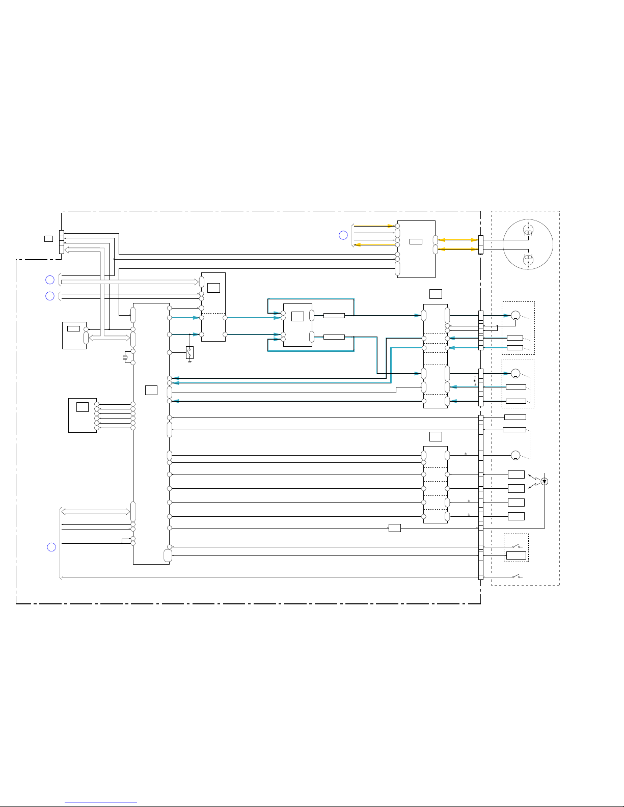
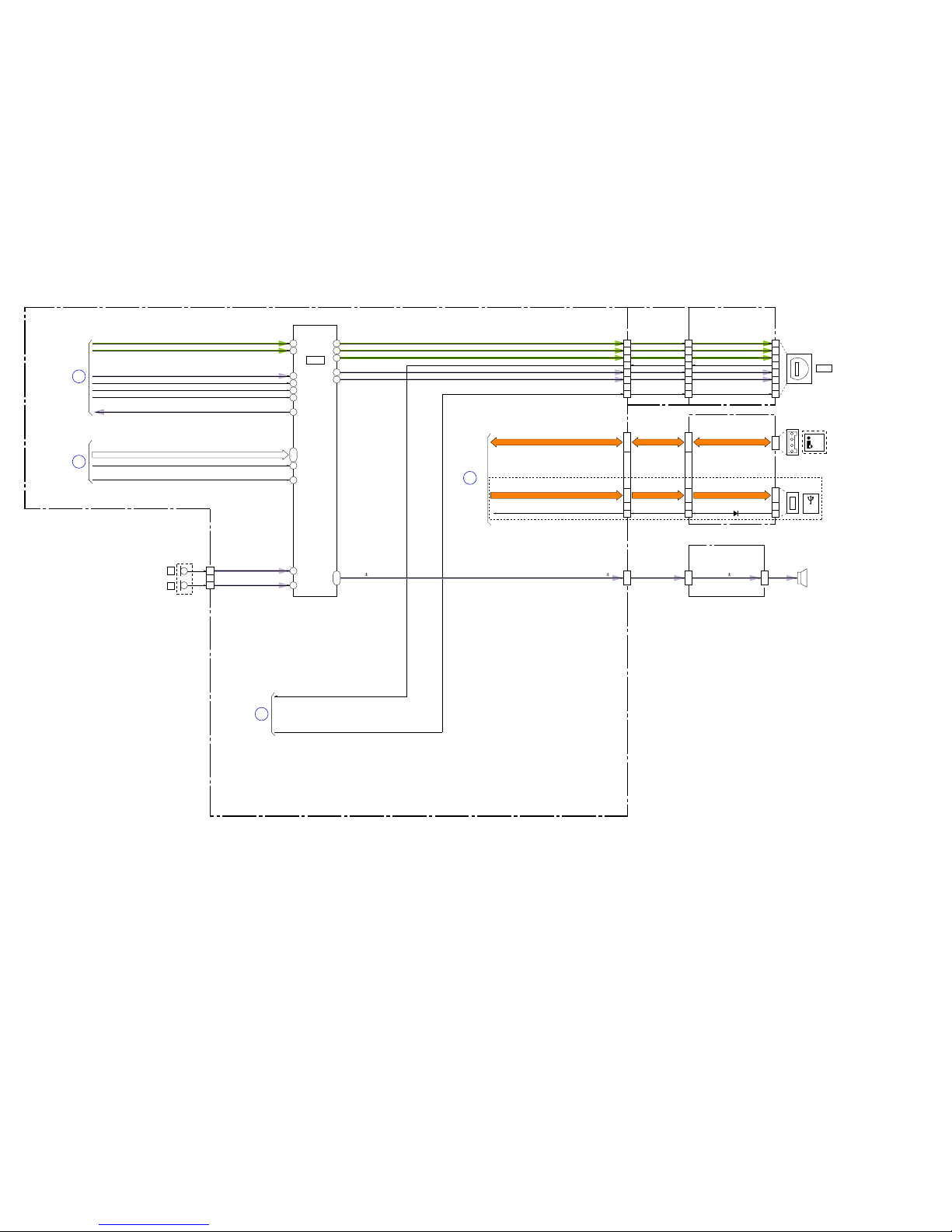
3-3. OVERALL BLOCK DIAGRAM (3/5)
( ) : Number in parenthesis ( ) indicates the division number of schematic diagram where the component is located.
VC-537 BOARD (3/5)
OVERALL (1/5)
(PAGE 3-1)
6
OVERALL (5/5)
(PAGE 3-5)
11
OVERALL (1/5)
(PAGE 3-1)
3
A : VIDEO SIGNAL
PANEL_R
PANEL_G
PANEL_B
TP_Y
TP_SEL1
TP_X
XCS_EVF
EVF_BL_ON
PANEL_BL_ON
PANEL_HD, PANEL_VD
LB-137 BOARD
COLOR
EVF
UNIT
PD-358 BOARD (1/2)
FP-625 FLEXIBLE
BOARD (1/2)
EVF
LED_K
BACKLIGHT
DRIVE
Q9306
CN6404
5
2
6
3
TP_L
TP_R
TP_BOT
TP_TOP
TOUCH
PANEL
TOUCH
PANEL
I/F
Q6401, Q6402
2.5 inch
COLOR
LCD
UNIT
34
21
22
26
10
28
20
42, 45, 44
5, 11, 18
48, 1
R
G
B
COM, CS
COM_P
EVF_COM_CS
EVF_STBY
EVF_STB STB
LED_K
COM
RGT_P, DWN_P, XSTBY_P RGT, DWN, XSTBY RGT, DWN, XSTBY
CN6405
HCK1, HCK2, HST,
PCG, EN, VCK, VST,
WIDE, PSIG, REF
33
32
6 - 9, 12,
14, 16, 17,
24, 30
LCD901
31
5
3
7
6
1
2
43
3
LCD
BACKLIGHT
DRIVE
Q9312 - Q9315
XSYS_RST
VR
VG
VB
COM, CS
18
16
17
CN302
D302
(BACKLIGHT)
D6403 - D6405
(BACKLIGHT)
EVF_VR
EVF_VG
EVF_VB
EVF_COM_CS
14
13
17
15
CN9301
EVF_HCK1, EVF_HCK2,
EVF_HST, EVF_PCG,
EVF_EN, EVF_VCK, EVF_VST,
WIDE, EVF_VP, EVF_REF
HCK1, HCK2, HST,
PCG, EN, VCK, VST,
WIDE, PSIG, REF
HCK1, HCK2, HST,
PCG, EN, VCK, VST,
BLK, PSIG, REF
EVF_HCK1, EVF_HCK2, EVF_HST,
EVF_PCG, EVF_EN, EVF_VCK, EVF_VST,
WIDE, EVF_VP, EVF_REF
LCD/EVF
DRIVE
(13/13)
IC9301
LCD/EVF
BACKLIGHT
CONTROL
(13/13)
IC9302
LCD902
20
7
8
4
6
CN301
1
7
14 11
VD_SI, VD_SO, VD_SCK
CN9302
(1/2)
1
2
3
30
14
16
15
PANEL_VR
PANEL_VG
PANEL_VB
EVF_VR
EVF_VG
EVF_VB
TP_Y
TP_SEL1
BL_H1 - BL_H3
TP_X
TP_Y
TP_SEL1
BL_H1 - BL_H3
TP_X
CN6401
(1/2)
30
29
28
17
15
16
19 - 23, 29, 28, 7, 24, 17 3 - 6, 8 - 12, 16
21, 19
18 - 15, 13 - 9, 5
5 - 7, 9, 10, 12 - 15, 20
5
3
4
24, 23
6 - 9, 11 - 13, 20 - 222, 19, 14
27 - 25
1
12 - 8, 2, 3, 24, 7, 144 - 6
11 - 9
20 - 22
3-4
DCR-HC51E/HC52/HC52E/HC53E/HC54/HC54E_L2
3-4. OVERALL BLOCK DIAGRAM (4/5)
( ) : Number in parenthesis ( ) indicates the division number of schematic diagram where the component is located.
SP
L
R
MIC901
MICROPHONE
VC-537 BOARD (4/5)
CN1001
1
3
INT_MIC_L
INT_MIC_R
VIDEO OUT,
AUDIO I/O
(8/13)
IC6701
33
44
32
18
21
20
24
22
23
16
42
14
12
11
CN2001
(1/2)
26, 27
2, 4
VSP_SO, XVSP_SCKVSP_SO, XVSP_SCK
OVERALL (1/5)
(PAGE 3-1)
4
OVERALL (1/5)
(PAGE 3-1)
7
OVERALL (5/5)
(PAGE 3-5)
12
DATA_TO_SFD
SFD_BCK
DATA_FROM_SFD
SFD_FCK
SFD_LRCK
28
47
BEEP
XCS_AU1
IC_6001_C_OUT
IC_6001_Y_OUT
CN402
VIDEO_I/O
MULTI_JACK_IN
AUDIO_L_I/O
AUDIO_R_I/O
S_C_I/O
S_Y_I/O
MULTI_JACK_IN
VIDEO_OUT
AUDIO_L_I/O
AUDIO_R_I/O
S_C_OUT
S_Y_OUT
VIDEO_IN/OUT
S-C
S-Y
JACK_AD
AUDIO_R
AUDIO_L
AV-125 BOARDFP-626 FLEXIBLE
BOARD (1/2)
26
27
29
28
24
23
LANC_SIG
10
5
9
1
6
7
A/V R
CN401
4
LANC_SIG
LANC_SIG
21
2
11
8
9
3
5
6
A : VIDEO SIGNAL
A : AUDIO SIGNAL
A : VIDEO/AUDIO SIGNAL
SP SP
SP901
SPEAKER
CF-111 BOARD (1/3)
CN1016 CN101
CN1002
(1/3)
9, 10
CN801
1, 2
CN802
(1/3)
2, 1
OVERALL (1/5)
(PAGE 3-1)
5
(USB)
CN103
1
CN104
TPA, NTPA, TPB, NTPB
D+, D-
VCCUSB_DETUSB_DET
D101
9
6 - 94, 3
2 - 5
4 - 1
7, 8
3, 2
2
JK-367 BOARD
USB_DET
DV
TPA+, TPA-, TPB+, TPB- TPA+, TPA-, TPB+, TPB-
USB_D+, USB_D-USB_D+, USB_D-
HC53E/HC54/HC54E
 Loading...