

Sony Handycam DCR-HC16E, Handycam DCR-HC18E, Handycam DCR-HC20E, Handycam DCR-HC20 Service Manual
SERVICE MANUAL
LEVEL 2
• For ADJUSTMENTS (SECTION 6), refer to SERVICE MANUAL, ADJ (987670451.pdf).
• For INSTRUCTION MANUAL, refer to SERVICE MANUAL, LEVEL 1 (987670441.pdf).
• For MECHANISM ADJUSTMENTS, refer to the “DV MECHANICAL ADJUSTMENT MANUAL
Z (Z200) MECHANISM ” (9-876-724-11).
• Reference number search on printed wiring boards is available.
• Table for differences of function of each model.
Link
SERVICE NOTE
DISASSEMBLY
BLOCK DIAGRAMS
FRAME SCHEMATIC DIAGRAMS
SCHEMATIC DIAGRAMS
PRINTED WIRING BOARDS
REPAIR PARTS LIST
SPECIFICATIONS
SERVICE NOTE
DISASSEMBLY
BLOCK DIAGRAMS
FRAME SCHEMATIC DIAGRAMS
SCHEMATIC DIAGRAMS
PRINTED WIRING BOARDS
REPAIR PARTS LIST
SPECIFICATIONS
Link
Revision History
Revision History
On the VC-350 board
This service manual provides the information that is premised the circuit board replacement service and not intended repair
inside the VC-350 board.
Therefore, schematic diagram, printed wiring board, waveforms, mounted parts location and electrical parts list of the VC-350
board are not shown.
The following pages are not shown.
Mounted parts location .............................
Pages 4-67 to 4-68
Electrical parts list ................................... Pages 5-16 to 5-21
How to use
Acrobat Reader
How to use
Acrobat Reader
Schematic diagram .............................Pages 4-19 to 4-44
Printed wiring board ............................Pages 4-59 to 4-62
Ver 1.2 2004. 07
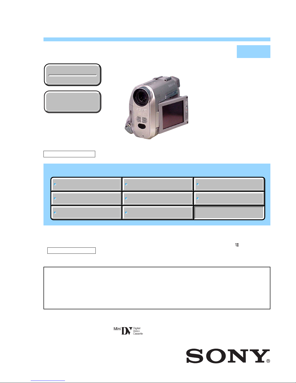
DIGITAL VIDEO CAMERA RECORDER
Photo : DCR-HC20E
DCR-HC16E/HC18E/
HC20/HC20E
RMT-830
DCR-HC20
US Model
Canadian Model
Korea Model
DCR-HC16E/
HC18E/HC20E
AEP Model
East European Model
North European Model
DCR-HC18E/HC20E
UK Model
DCR-HC20/HC20E
E Model
Tourist Model
DCR-HC20E
Australian Model
Chinese Model
Hong Kong Model
Z (Z200) MECHANISM

— 2 —
DCR-HC16E/HC18E/HC20/HC20E
SPECIFICATIONS
System
Video recording s ystem
2 rotary heads, Helical scann ing system
Audio recordin g s y s tem
Rotary heads, PCM system
Quantization: 12 bits (Fs 32 kHz, stereo 1,
stereo 2), 16 bits (Fs 48 kHz, stereo)
Video signal
DCR-HC20 :
PAL color, CCIR standards
DCR-HC16E/HC18E/HC20E :
Usable cassette
Mini DV cassette with the mark
printed
Tape speed
SP: Approx. 18.81 mm/s
LP: Approx. 12.56 mm/s
Recording/playback time (using a DVM60
cassette)
SP: 60 min
LP: 90 min
Fast forward/rewind time (using a DVM60
cassette)
Approx. 2 min 40 sec.
Viewfinder
Electric viewfinder (black and white)
Image device
3 mm (1/6 type) CCD (Charge Co upl ed
Device)
Gross: Approx. 800 000 pixels
Effective (movie ): A pprox. 400 000 pixels
Lens
Carl Zeiss Vario Tessar
Combined power zoom lens
Filter diameter: 25 mm (1 in.)
10
× (Optical),
10
× (Optical),
100
× (Digital)
120
× (Digital)
F = 1.7 ~ 2.3
Focal length
2.3 - 23 mm (3/32 - 29/32 in.)
When converted to a 35 mm still camera
In CAMERA:
43 - 430 mm (1 3/4 - 17 in.)
[ AUTO], [ONE PUSH], [INDOOR] (3
200 K), [OUTDOOR] (5 800 K)
Minimum illumination
5 lx (lux) (F 1.7)
0 lx (lux) (during the NightShot plu s
function)*
* Objects unable to be seen due to the dark can be
shot with infrared lighting.
Input/Output connectors
Audio/Video output
10-pin connector
Video signal: 1 Vp- p , 75
Ω (ohms),
unbalanced
Luminance signal: 1 Vp-p, 75
Ω (ohms),
unbalanced
Chrominance signal: 0.3 Vp-p, 75
Ω (ohms),
unbalanced
Audio signal: 327 mV (at outp ut i mp edance
more than 47 k
Ω (kilohms)), Output
impedance with less than 2.2 k
Ω (kilohms)
DV input (For DCR-HC20/HC20E)/output
4-pin connector
LANC jack
Stereo mini-minijack (ø 2.5 mm)
USB jack
mini-B
MIC jack
Minijack, 0.38 8 mV lo w impedance with DC
2.5 to 3.0 V, output impedance 6.8 k
Ω
(kilohms) (ø 3.5 mm), Stereo type
LCD screen
Picture
6.2 cm (2.5 type)
Total dot number
123 200 (560
× 220)
General
Power requirements
DC 7.2 V (battery pack )
DC 8.4 V (AC Adaptor)
Average power consumption (when using the
battery pack)
During camera re cor di ng usi n g the v iewf i nder
2.2 W
During camera recording using the LCD
2.5 W
Operating temperature
0°C to 40°C (32°F to 104°F)
Storage temperature
-20°C to + 60°C (-4°F to + 140° F)
Dimensions (approx.)
50
× 86 × 112 mm (2 × 3 1/2 ×4 1/2 in.)
(w/h/
d)
Mass (approx.)
380 g (13 oz) main unit only
440 g (15 oz) including the NP-FP50
rechargeable battery pack and DVM60
cassette.
Supplied accessories
See page 5-12.
AC Adaptor AC-L25A/L25B
Power requirements
AC 100 - 240 V, 50/60 Hz
Current consumption
0.35 - 0.18 A
Power consumption
18 W
Output voltage
DC 8.4 V, 1.5 A
Operating temperature
0°C to 40° C (32° F to 104°F)
Storage temperature
-20°C to + 60°C (-4°F to + 140°F)
Dimensions (approx.)
56
× 31 × 100 mm (2 1/4 × 11/4 × 4 in.)
(w/h/d) exclud ing the projecting parts
Mass (approx.)
190 g (6.7 oz) excluding the mains lead
Rechargeable battery pack (NP-FP50)
Maximum output voltage
DC 8.4 V
Output voltage
DC 7.2 V
Capacity
4.9 Wh (680 mAh)
Dimensions (approx.)
31.8
× 18.5 × 45.0 mm
(1 5/16
× 3/4 × 1 13/16 in.) (w/h/d)
Mass (approx.)
40 g (1.5 oz)
Operating temperature
0°C to 40° C (32° F to 104°F)
Type
Lithium ion
Design and specifications are subject to change
without notice.
NTSC color, EIA standards
Video camera recorder
DCR-HC20 :
DCR-HC16E :
DCR-HC18E/HC20/HC20E :
DCR-HC16E/HC18E/HC20E :
Gross: Approx. 680 000 pixels
Effective (movie): Approx. 340 000 pixels
Color temper ature
DCR-HC20 :
DCR-HC16E/HC18E/HC20E :
Chrominance signal: 0.286 Vp-p, 75 Ω
(ohms), unbalanced
— 3 —
DCR-HC16E/HC18E/HC20/HC20E
1. Check the area of your repair for unsoldered or poorly-soldered
connections. Check the entire board surface for solder splashes
and bridges.
2. Check the interboard wiring to ensure that no wires are
"pinched" or contact high-wattage resistors.
3. Look for unauthorized replacement parts, particularly
transistors, that were installed during a previous repair . Point
them out to the customer and recommend their replacement.
4. Look for parts which, through functioning, show obvious signs
of deterioration. Point them out to the customer and
recommend their replacement.
5. Check the B+ voltage to see it is at the values specified.
6. Flexible Circuit Board Repairing
• Keep the temperature of the soldering iron around 270˚C
during repairing.
• Do not touch the soldering iron on the same conductor of the
circuit board (within 3 times).
• Be careful not to apply force on the conductor when soldering
or unsoldering.
Unleaded solder
Boards requiring use of unleaded solder are printed with the leadfree mark (LF) indicating the solder contains no lead.
(Caution: Some printed circuit boards may not come printed with
the lead free mark due to their particular size.)
: LEAD FREE MARK
Unleaded solder has the following characteristics.
• Unleaded solder melts at a temperature about 40°C higher than
ordinary solder.
Ordinary soldering irons can be used but the iron tip has to be
applied to the solder joint for a slightly longer time.
Soldering irons using a temperature regulator should be set to
about 350°C.
Caution: The printed pattern (copper foil) may peel away if the
heated tip is applied for too long, so be careful!
• Strong viscosity
Unleaded solder is more viscous (sticky , less prone to flo w) than
ordinary solder so use caution not to let solder bridges occur such
as on IC pins, etc.
• Usable with ordinary solder
It is best to use only unleaded solder but unleaded solder may
also be added to ordinary solder.
SAFETY CHECK-OUT
After correcting the original service problem, perform the following
safety checks before releasing the set to the customer.
SAFETY-RELATED COMPONENT WARNING!!
COMPONENTS IDENTIFIED BY MARK 0 OR DOTTED LINE WITH
MARK 0 ON THE SCHEMATIC DIAGRAMS AND IN THE PARTS
LIST ARE CRITICAL TO SAFE OPERATION. REPLACE THESE
COMPONENTS WITH SONY PARTS WHOSE PART NUMBERS
APPEAR AS SHOWN IN THIS MANUAL OR IN SUPPLEMENTS
PUBLISHED BY SONY .
ATTENTION AU COMPOSANT AYANT RAPPORT
À LA SÉCURITÉ!
LES COMPOSANTS IDENTIFÉS P AR UNE MARQUE 0 SUR LES
DIAGRAMMES SCHÉMA TIQUES ET LA LISTE DES PIÈCES SONT
CRITIQUES POUR LA SÉCURITÉ DE FONCTIONNEMENT. NE
REMPLACER CES COMPOSANTS QUE PAR DES PIÈSES SONY
DONT LES NUMÉROS SONT DONNÉS DANS CE MANUEL OU
DANS LES SUPPÉMENTS PUBLIÉS PAR SONY.
CAUTION :
Danger of explosion if battery is incorrectly replaced.
Replace only with the same or equivalent type.
PAL
960H-P
✕
DCR-HC16E
AEP, NE, EE
✕
100 ×
DCR-
HC18E
AEP, UK, NE, EE
DCR-
HC20E
AEP, UK, NE, EE,
E, CH, AUS, HK, JE
PAL
960H-P
Table for difference of function
Model
Destination
Color System
Remote Commander
Lens
Optical
Digital
CCD Imager
DV Input
DCR-
HC20
US, CND, E
,
KR, JE
NTSC
a
120 ×
960H
a
10 ×
• Abbreviation
CND : Canadian model
EE : East European model
NE : North European model
AUS : Australian model
HK : Hong Kong model
CH : Chinese model
KR : Korea model
JE : Tourist model

— 4 —
DCR-HC16E/HC18E/HC20/HC20E
TABLE OF CONTENTS
1. SERVICE NOTE
1-1. SERVICE NOTE ·····························································1-1
1. NOTE FOR REPAIR ······················································· 1-1
2. POWER SUPPLY DURING REPAIRS ··························1-2
3. TO TAKE OUT A CASSETTE WHEN NOT EJECT
(FORCE EJECT) ·····························································1-2
2. DISASSEMBLY
2-1. DISASSEMBLY······························································2-1
2-2. SERVICE POSITION ····················································· 2-3
2-3. CIRCUIT BOARDS LOCATION ···································2-6
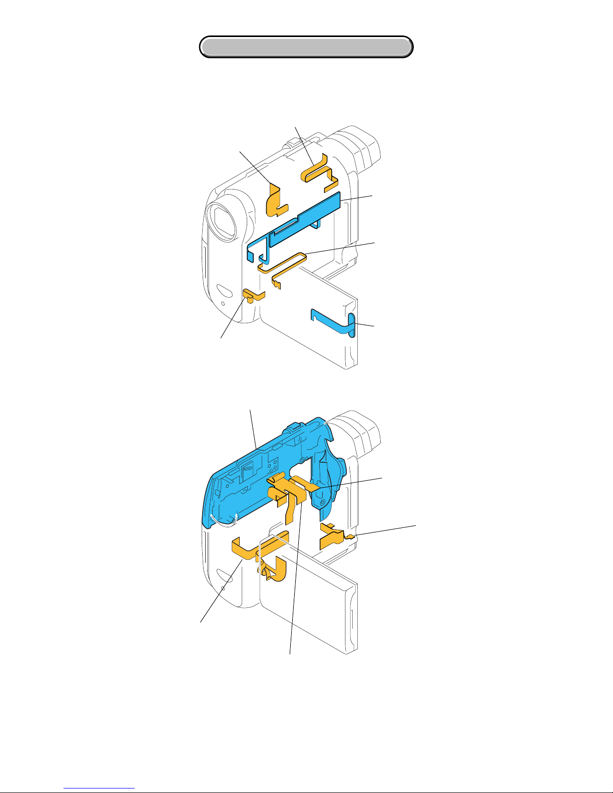
2-4. FLEXIBLE BOARDS LOCATION ································2-7
HELP (List of caution points is shown here.)
3. BLOCK DIAGRAMS
3-1. OVERALL BLOCK DIAGRAM (1/4) ···························3-1
3-2. OVERALL BLOCK DIAGRAM (2/4) ···························3-3
3-3. OVERALL BLOCK DIAGRAM (3/4) ···························3-5
3-4. OVERALL BLOCK DIAGRAM (4/4) ···························3-7
3-5. POWER BLOCK DIAGRAM (1/3)································3-9
3-6. POWER BLOCK DIAGRAM (2/3)······························3-11
4. PRINTED WIRING BOARDS AND
SCHEMATIC DIAGRAMS
4-1. FRAME SCHEMATIC DIAGRAM (1/2)······················· 4-1
FRAME SCHEMATIC DIAGRAM (2/2)·······················4-3
4-2. SCHEMATIC DIAGRAMS
• CD-489 (CCD IMAGER)
SCHEMATIC DIAGRAM ······························4-7
• PD-213 (LCD RGB DRIVE, BACKLIGHT)
SCHEMATIC DIAGRAM ······························4-9
• CONTROL KEY BLOCK (SB6300)
SCHEMATIC DIAGRAM ······························4-9
• LB-095 (EVF RELAY)
SCHEMATIC DIAGRAM ····························4-11
• SE-141 (PITCH/YAW SENSOR AMP)
SCHEMATIC DIAGRAM ····························4-12
• JK-260 (JACK)
SCHEMATIC DIAGRAM ····························4-13
• FP-830 FLEXIBLE (BAT/DC IN)
SCHEMATIC DIAGRAM ····························4-14
• IR-051 (REMOTE COMMANDER RECEIVER,
MIC IN)
SCHEMATIC DIAGRAM ····························4-15
• MS-200 (INDICATOR)
SCHEMATIC DIAGRAM ····························4-15
• CONTROL KEY BLOCK (SS6300, CF6300)
SCHEMATIC DIAGRAM ····························4-17
• FP-836 (PANEL REVERSE)
SCHEMATIC DIAGRAM ····························4-18
Shematic diagram of the VC-350 board is not sho wn.
Pages from 4-19 to 4-44 are not shown.
• FP-228/467/826 FLEXIBLE (S/T REEL SENSOR,
TAPE SENSOR)
SCHEMATIC DIAGRAM ····························4-45
4-3. PRINTED WIRING BOARDS ·····································4-49
• CD-489 (CCD IMAGER)
PRINTED WIRING BOARD ·······················4-49
• IR-051 (REMOTE COMMANDER RECEIVER,
MIC IN)
PRINTED WIRING BOARD ·······················4-49
• JK-260 (JACK)
PRINTED WIRING BOARD ·······················4-51
• LB-095 (EVF RELAY)
PRINTED WIRING BOARD ·······················4-53
• SE-141 (PITCH/YAW SENSOR AMP)
PRINTED WIRING BOARD ·······················4-53
• PD-213 (LCD RGB DRIVE, BACKLIGHT)
PRINTED WIRING BOARD ·······················4-55
• MS-200 (INDICATOR)
PRINTED WIRING BOARD ·······················4-57
Printed wiring board of the VC-350 board is not shown.
Pages from 4-59 to 4-62 are not shown.
• FP-228/467/826 FLEXIBLE BOARD
(S/T REEL SENSOR, TAPE SENSOR) ·······4-63
4-4. MOUNTED PARTS LOCATION ·································4-65
Mounted parts location of the VC-350 board is not sho wn.
Pages from 4-67 to 4-68 are not shown.
5. REPAIR PARTS LIST
5-1. EXPLODED VIEWS ······················································ 5-3
5-1-1.OVERALL SECTION····················································· 5-3
5-1-2.CABINET (R) SECTION ···············································5-4
5-1-3.LCD SECTION ·······························································5-5
5-1-4.BAT. EVF SECTION ······················································5-6
5-1-5.LENS SECTION ·····························································5-7
5-1-6.CABINET (L) SECTION················································5-8
5-1-7.OVERALL (MECHANISM DECK-Z200)·····················5-9
5-1-8.LS CHASSIS BLOCK ASSEMBLY·····························5-10
5-1-9.MECHANICAL CHASSIS BLOCK ASSEMBLY·······5-11
Checking supplied accessories ················································5-12
5-2. ELECTRICAL PARTS LIST ········································5-13
Electrical parts list of the VC-351 board is not shown.
Pages from 5-16 to 5-21 are not shown.
1-1
SECTION 1
SERVICE NOTE
DCR-HC16E/HC18E/HC20/HC20E
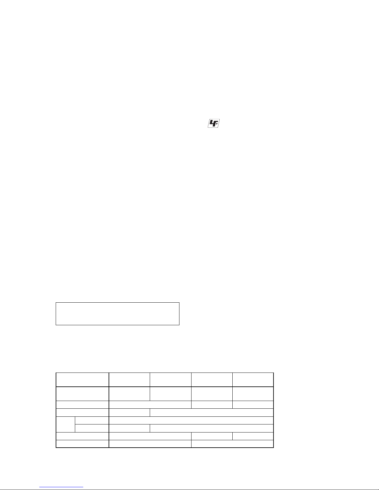
Make sure that the flat cable and flexible board are not cracked of
bent at the terminal.
Do not insert the cable insufficiently nor crookedly.
Cut and remove the part of gilt
which comes off at the point.
(Take care that there are
some pieces of gilt left inside)
When remove a connector, don't pull at wire of connector.
Be in danger of the snapping of a wire.
When installing a connector, don't press down at wire of connector.
Be in danger of the snapping of a wire.
1-1. SERVICE NOTE
1. NOTE FOR REPAIR
1-2E
DCR-HC16E/HC18E/HC20/HC20E
2. POWER SUPPLY DURING REPAIRS
In this unit, about 10 seconds after power is supplied to the battery terminal using the regulated power supply (8.4V), the po wer is shut of f so
that the unit cannot operate.
This following two methods are available to prevent this. Take note of which to use during repairs.
Method 1.
Use the AC power adaptor.
Method 2.
Connect the servicing remote commander RM-95 (J-6082-053-B) to the LANC jack, and set the commander switch to the “ADJ” side.
3. TO TAKE OUT A CASSETTE WHEN NOT EJECT (FORCE EJECT)
1 Remove the cabinet (R) section.
2 Remove the front panel block assembly.
3 Remove the BAT, EVF block assembly.
4 Remove the lens block assembly.
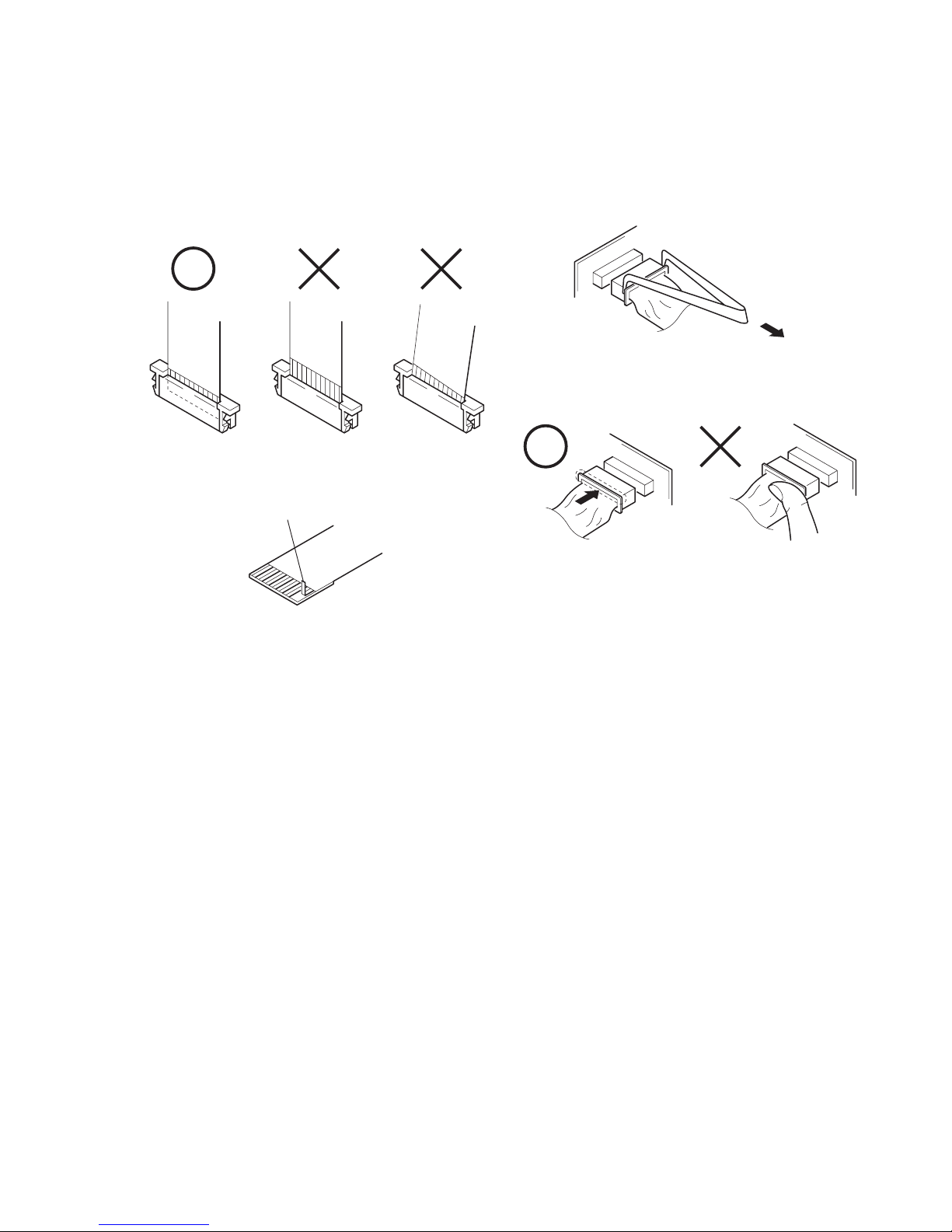
5 Remove the mechanism deck and the VC-350 board.
6 Open the VC-350 board.
7 Disconnect CN9002 (27P, 0.3mm) of VC-350 board.
8 Supply +4.5V from the DC power supply to the loading motor and unload with pressing the cassette compartment.
VC-350
CN9002
VC-350 board
DC power supply (+4.5Vdc)
Loading motor
Disconnect the flexible board from
CN9002 of VC-350 board.
DCR-HC16E/HC18E/HC20/HC20E
2-1 2-2
2-1. DISASSEMBLY
The following flow chart shows the disassembly procedure.
VC
-350
V
C
-350
V
C
-350
VC
-350
VC
-350
VC
-350
3
2
3
2
6
qs
4
2
3
5
6
1
4
7
1
8
5
4
3
1
2
7
0
9
4
4
5
6
7
8
0
9
qa
3
8
6
7
2
4
5
3
3
5
2
3
1
2
1
1
2
3
1
9
4
6
1
Shoe cover
2
Two special screws (M2x2.8) silver
3
Cold shoe
1
Two screws (M1.7x3) silver
2
Five tapping screws (M1.7x4) black
3
Screw (M1.7x3) silver
4
Open the G cabinet (64) assembly.
5
Two claws
1
Two tapping screws (M1.7x6) black
2
Hinge blind
3
LCD section
4
Cabinet (R) section
1
Two screws (M1.7x3) silver
2
Two tapping screws (M1.7x5) black
3
P cabinet (C) assembly
4
Tape (A)
5
FP-835 flexible board (22P)
6
Hinge section
1
Screw (M1.7 × 2.5) black
2
Four claws
3
Hinge cover (M),
FP-836 flexible boar
d
4
Hinge cover (C)
5
FP-835 flexible board, Hinge section
1
Two tapes (W)
2
Screw (M1.7x2.5) black
3
From lens flexible board (23P)
4
SS6300 control key block (18P)
5
to qa (CN1005 (20P), CN1008 (39P), CN6501 (10P), CN9001 (10P), CN9002 (27P),
CN9003 (27P), CN3001 (14P)) of VC-350 board
qs
VC-350 board
1
Two tapes (W)
2
From lens flexible board (23P)
3
FP-833 flexible board (6P)
4
FP-827 flexible board (14P)
5
Two screws (M1.7x2.5) black
6
Lens block assembly
1
Screw (M1.7x3) silver
2
BAT section
3
EVF section
1
Two tapping screws (M1.7x5) black
2
Two screws (M1.7x3) silver
3
P cabinet (C) assembly
qa
qs
7
SB6300 control key block (6P)
8
Tapping screw (M1.7x5) black
9
Two claws
0
Panel cushion
qa
P cabinet (M) assembly
qs
PD-213 board, LCD unit (ACX528AKN-J),
Light guide plate block
7
FP-836 flexible board (6P)
8
FP-835 flexible board (22P)
9
Cabinet (R) section
5
FP-830 flexible board (26P)
6
FP-831 flexible board (20P)
7
BAT, EVF block assembly
HELP 01
1
2
5
3
4
2
1
1
3
4
7
3
1
2
5
6
1
FP-833 flexible board (39P)
2
FP-832 flexible board (20P)
3
SS6300 control key block (18P)
4
Screw (M1.7x2.5) black
5
Two screws (M1.7x2.5) black
6
Open the G cabinet (64) assembly.
7
VC-350 board, Mechanism deck, MD frame assembly
FFC-036 flexible board
2
1
Screw (M1.7x4) black
2
Screw (M1.7x2.5) black
3
Screw (M1.7x4) black
4
Two tapes (A)
7
6
2
4
3
1
1
Open the G cabinet (64) assembly.
2
Screw (M1.7x2.5) black
3
Eject knob
4
Six tapping screws (M1.7x4) silver
5
Two screws (M1.7x2.5) black
6
FP-832 flexible board
7
G cabinet (64) assembly, MS-200 board,
FP-832 flexible board
HELP 03
5
5
1
2
3
1
Shoe cover
2
Tapping screw (M1.7x5) black
3
EYE cup assembly
1
1
Three screws (M1.7x3) silver
2
FFC-036 flexible flat cable (16P)
3
Claw
4
F panel block assembly
5
Cushion (F2)
6
CF6300 control key block (8P)
HELP 02
(disassembly of the EVF section)
SECTION 2
DISASSEMBLY
2. DISASSEMBLY
2. DISASSEMBLY
DCR-HC16E/HC18E/HC20/HC20E
2-3 2-4
2-2. SERVICE POSITION
VC
-350
VC
-350
VC-350
VC-350
VC-350
JK-260
VC-350
AC power
adaptor
AC IN
1
8
[SERVICE POSITION TO CHECK THE VTR SECTION]
Connection to Check the VTR Section
To check the VTR section, set the VTR to the "Forced VTR power ON" mode.
Operate the VTR functions using the touch panel or the adjustment remote commander (HOLD switch: OFF position).
Setting the "Forced VTR Power ON" mode
1) Select page: 0, address: 01, and set data: 01.
2) Select page: 0, address: 10, and set data: 00.
3) Select page: D, address: 10, set data: 02, and press the
PAUSE button of the adjustment remote commander.
To eject a cassette, connect the
control key block (SS6300)
Exiting the "Forced VTR Power ON" mode
1) Select page: 0, address: 01, and set data: 01.
2) Select page: 0, address: 10, and set data: 00.
3) Select page: D, address: 10, set data: 00, and press the
PAUSE button of the adjustment remote commander.
4) Select page: 0, address: 01, and set data: 00.
Adjustment remote
commander (RM-95)
Cabinet (R) section
FP-835 Flexible
board (22P)
FP-833 Flexible
board (39P)
FP-830 Flexible
board (26P)
JK-260 board
CN1006
CN9003
CN9002
CN9001
CN6501
CN1008
CN1001
CN1007
CN2001
VC-350 board
Mechanism deck
SS6300 Control key block (18P)
BAT section
LANC
DC-IN
CPC-15
(J-6082-564-A)
I/F unit for LANC control
(J-6082-521-A)
2
1
3
4
3
5
2
1
8
6
7
2
4
5
3
1
9
3
5
6
4
7
1
2
3
2
1
3
2
6
4
5
1
4
7
3
1
2
5
6
7
6
2
4
3
1
5
2-5
DCR-HC16E/HC18E/HC20/HC20E
P
D
-2
1
3
[PD-213 BOARD SERVICE POSITION]
1
3
2
PD-213 board
AC power
adaptor
AC IN
Adjustment remote
commander (RM-95)
LANC
2. DISASSEMBLY
2. DISASSEMBLY
2-6
DCR-HC16E/HC18E/HC20/HC20E
2. DISASSEMBLY
2. DISASSEMBLY
2-3. CIRCUIT BOARDS LOCATION
VC-350
SE-141
LB-095
CD-489
MS-200
IR-051
PD-213
JK-260
CD-489
IR-051
JK-260
LB-095
MS-200
PD-213
SE-141
NAME
FUNCTION
VC-350
CCD IMAGER
REMOTE COMMANDER RECEIVER, MIC IN
JACK
EVF RELAY
INDICATOR
LCD RGB DRIVE, BACKLIGHT
PITCH/YAW SENSOR AMP
TIMING GENERATOR, S/H, AGC, ADC., LENS DRIVE, CAMERA/DV SIGNAL/AUDIO PROCESSOR,
DV INTERFACE, VIDEO OUT, REC/PB AMP, DRUM/CAPSTAN/LOADING MOTOR DRIVE,
CAMERA/MECHA CONTROL, HI CONTROL, RGB DRIDE, D/A-A/D CONV., MIC AMP,
AUDIO OUT, POWER IN, CHARGE, DC/DC CONVERTER, CONNECTOR-1, CONNECTOR-2
2-7E
DCR-HC16E/HC18E/HC20/HC20E
2. DISASSEMBLY
2. DISASSEMBLY
2-4. FLEXIBLE BOARDS LOCATION
The flexible boards contained in the lens block is not shown.
FP-831
FP-836
FFC-036
CONTROL KEY BLOC
K
(CF6300)
CONTROL KEY BLOC
K
(SB6300)
FP-827
FP-830
FP-835
FP-833
CONTROL KEY BLOCK
(SS6300)
FP-832
DCR-HC16E/HC18E/HC20/HC20E
HELP
HELP
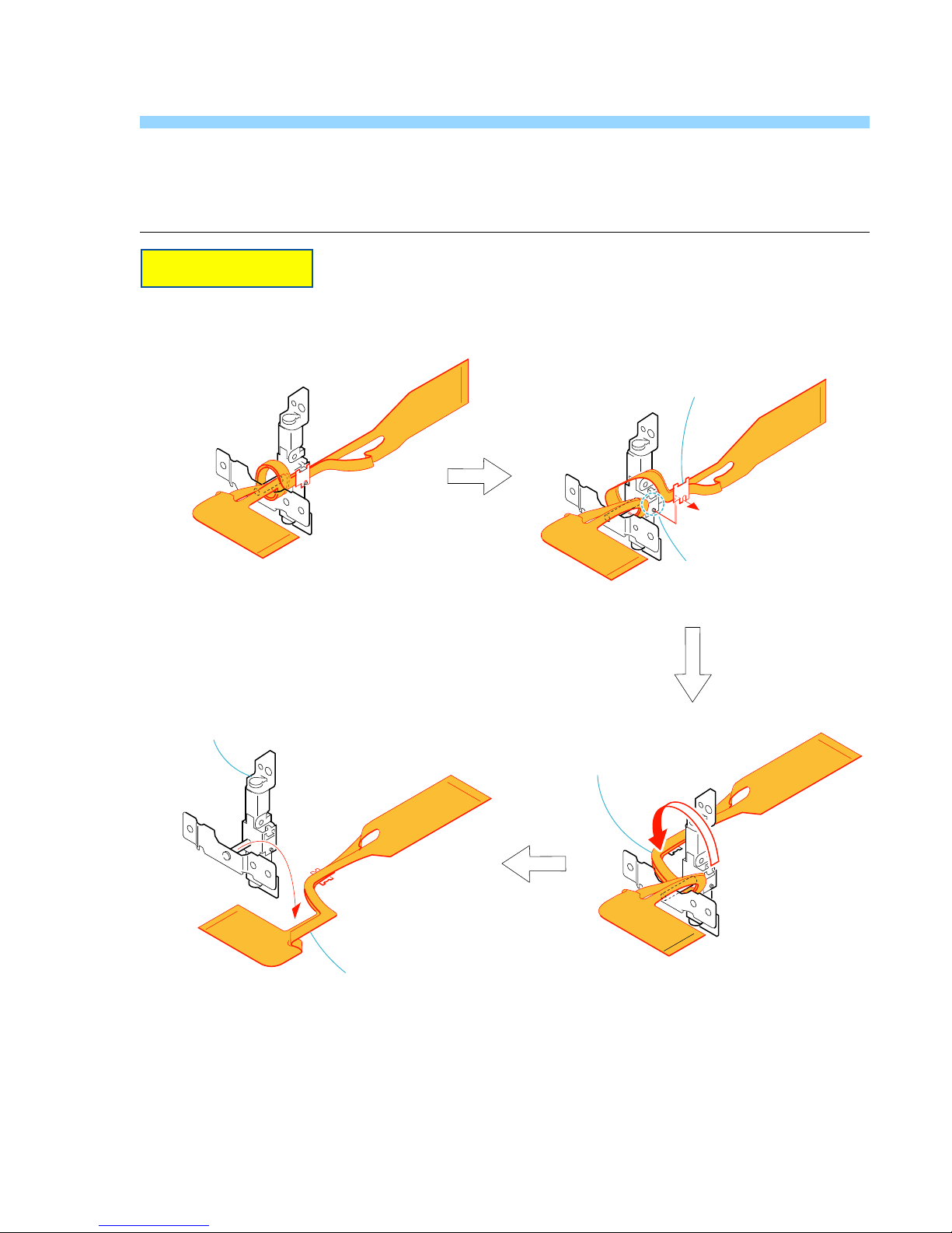
Sheet attachment positions and procedures of processing the flexible boards/harnesses are shown.
HELP 01
(disassembly of the Hinge section)
2
Unwind the FP-835 flexible
board wide open.
4
FP-835 flexible board
3
Hinge (63) assembly
1
Peel off the adhesive surface.
Adhesive surface
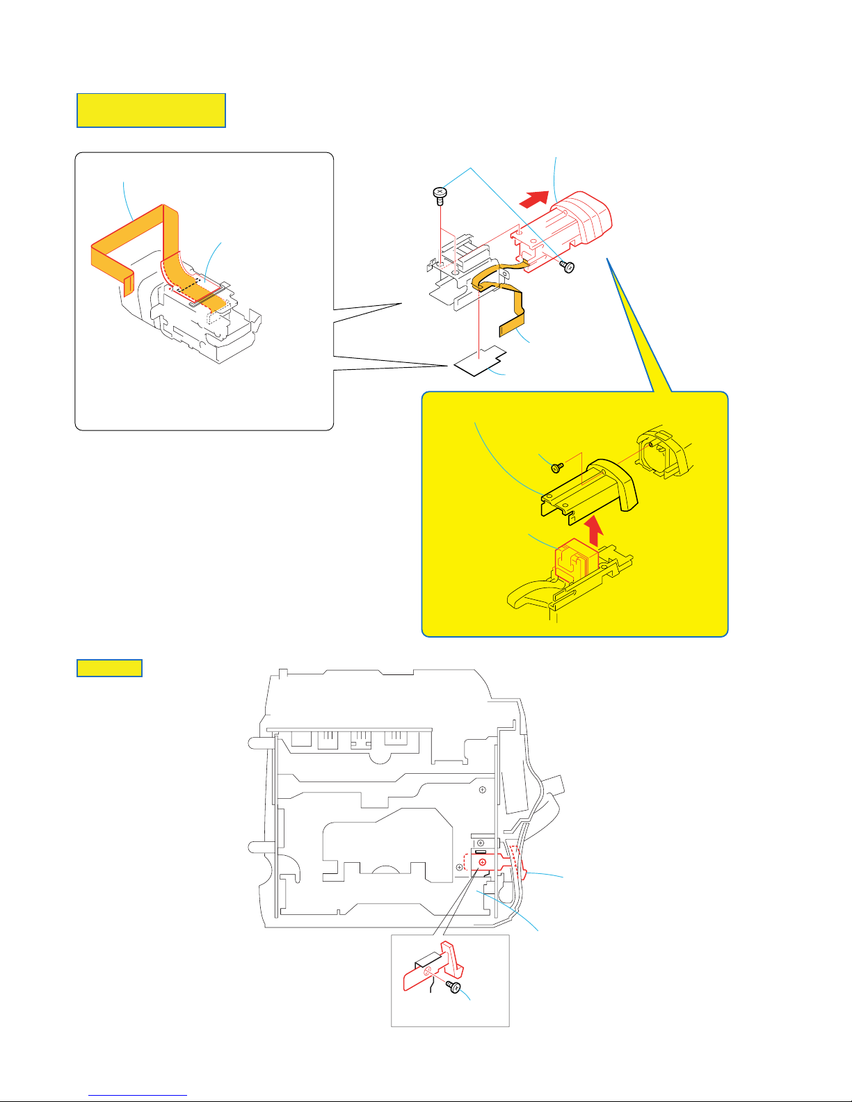
DCR-HC16E/HC18E/HC20/HC20E
HELP
HELP 02
(disassembly of the EVF section)
1
VF flexible fixfed sheet
4
Tapping screw
(M1.7
×
5), block
3
Slide the VF cabinet upper assembly,
etc, direction of the arrow.
FP-831 flexible board
VF flexible fixfed sheet
FP-831 flexible board
2
Three screws
(M1.7
×
3),
silver
Illuminator, Prism sheet
and other parts
Remove the VF cabinet upper assembly
in the direction of the arrow.
Eject knob
CS frame assembly
HELP 03
Screw (M1.7 × 2.5)
silver
DCR-HC16E/HC18E/HC20/HC20E
Link
Link
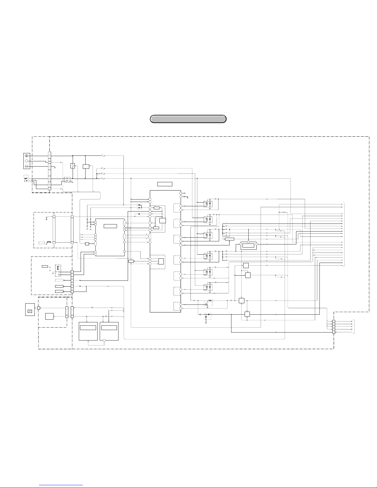
3. BLOCK DIAGRAMS
OVERALL BLOCK DIAGRAM (4/4)
POWER BLOCK DIAGRAM (1/2)
OVERALL BLOCK DIAGRAM (3/4)
OVERALL BLOCK DIAGRAM (2/4) POWER BLOCK DIAGRAM (2/2)
OVERALL BLOCK DIAGRAM (1/4)
OVERALL BLOCK DIAGRAM (4/4)
POWER BLOCK DIAGRAM (1/2)
OVERALL BLOCK DIAGRAM (3/4)
OVERALL BLOCK DIAGRAM (2/4) POWER BLOCK DIAGRAM (2/2)
OVERALL BLOCK DIAGRAM (1/4)
DCR-HC16E/HC18E/HC20/HC20E
3. BLOCK DIAGRAMS
3. BLOCK DIAGRAMS
3-1. OVERALL BLOCK DIAGRAM (1/4)
3-1 3-2
( ) : Number in parenthesis ( ) indicates the division number of schematic diagram where the component is located.
SECTION 3
BLOCK DIAGRAMS
JK-260
BOARD(2/4)
IC7302
D/A CONV.
A/D CONV.
IC7301
AUDIO
OUT
MIC
AMP
IC7001
VIDEO
OUT
Y
C
V
IC6002
DV
INTERFACE
29 37
23
X8601
20MHz
IC3002
CH SO,SCK
CAM SO,SI,SCK
16
TPA
NTPA
TPB
NTPB
ZOOM MOTOR
DRIVE
HALL AD
DV Interface
AD0-AD9 AD0-AD9
IRIS PWM
EN1,
DIR1 A,B
EN0,
DIR0 A,B
EN0,DIR0 A,DIR0 B
EN1,DIR1 A,DIR1 B
FC RST
ZM RST
IC3001
I DRIVE (–)
135
I HALL (–)
78
71
73
75
FC RST
ZM RST
128
77
CN1008
LCK0
TRCK0
TIMING
GENERATOR
CN704
FOCUS MOTOR
DRIVE
IC3102
94
CD-489 BOARD
IC3101
IRIS HALL AMP
IRIS DRIVE
VC-350 BOARD(1/4)
HALL AD
IRIS PWM
2
12
IC401
LENS ASSY
M
IC8601
18
PITCH AD
YAW/PITCH
8
H
IRIS
(SHUTTER)
SENSOR
YAW AD
AMP
129
YAW SENSOR
PITCH SENSOR
SE402
7
SE401
M
(1/2)
FOCUS
MOTOR
SE-141
BOARD
CAMERA CONTROL
ZOOM
MOTOR
ZOOM
RESET
SENSOR
M
CN3101
CCD
IMAGER
NIGHT SHOT
IRIS
METER
TO
OVERALL
BLOCK DIAGRAM
(3/4)
ZOOM VR AD
CN703
130
3
CN101
CN3001
1
187
TO
OVERALL
BLOCK DIAGRAM
(4/4)
(PAGE 3-8)
S/H,AGC
A/D CONV.
IC101
12
38
35
37
44
45
25
31
18
21
22
X3001
36MHz
4
5
VCK
CAM SO,SI,SCKCAM SO,SI,SCK
VCK
HD,VD
XSHD
XSHP
PBLK
CLPDM
|
2
11
CLPOB
HD,VD
CH SO,SCK
XNS SW
(2/13)
(2/13)
(1/13)
(1/13)
FC A,B
FC XA,XB
ZM A,B
ZM XA,XB
(6/13)
CN401 CN1008
47 48
1
16
15
2
23 19
FOCUS
RESET
SENSOR
30
1
(PAGE 3-5)
2
DV OUT Interface
JK-260
BOARD(1/4)
CN702
(USB)
CN704
CN1008
USB D+,D-
212423
175719
3
5
195
196
194
199
|
208
42
|
45
6
|
9
4
3
14
15
12
|
5
154
|
157
176
|
167
209
159
143
77
78
96
141
216
13
16
9
12
DO-D15
3
2
USB D+,D-
USB D+,D-
CAMERA
PROCESS
RF
SIGNAL
PROCESS
CHARACTER
GENERATOR
DV
SIGNAL
PROCESS
AUDIO
SIGNAL
PROCESS
USB
I/F
126
127
131
130
116
68
64
63
9
113
110
1
14
121
123
119
9
7
79
47
8
12
15
16
3
2
62
64
56
58
11
5
6
IC6001
27
26
VD,SO,SCK
MC BUSMC BUS
SPCK SPCK
RF INRF IN
REC CKREC CK
REC DTREC DT
SWP
FRRV
TRRT
TRRV
SWP
FRRV
TRRT
TRRV
SFD BCK
BW Y
EVF HD
EVF VD
PANEL HD
PANEL VD
CN1008
AUDIO R I/O
AUDIO L I/O
VIDEO I/O
LDATA FROM SFD
DATA FROM SFD
DATA TO SFD
DATA TO SFD
SFD BCK
R
L
R
L
R
PANEL R
PANEL G
PANEL B
BW Y
PANEL HD
PANEL VD
IC6001 Y OUT
PANEL R
PANEL G
PANEL B
TO
OVERALL
BLOCK DIAGRAM
(2/4)
(PAGE 3-3)
3
(3/13)
(3/13)
(9/13)
(9/13)
LBUS0-LBUS3
AUDIO SIGNAL
VIDEO SIGNAL
VIDEO/AUDIO SIGNAL
10
7
5
IC6001 C OUT
162
178
180
179
184
185
186
18
20
VSP SO,SI,SCKVSP SO,SI,SCK
(DCR-HC20/HC20E)
(DCR-HC16E/HC18E)
(3/13)
CCD OUT
V1-V4
RG,H1,H2
CN3001CN101
13
FP-827
(FLEXIBLE)
4-1 9 12 13
8-10
7-4
7-5
8-11
2
8
7
6
5
37
35
8
19
23
20
4
1
15
12
13
6
FP-833
(FLEXIBLE) (1/4)
25
26
42
46
39
49
SP+
SP-
SP+
SP-
INT MIC L
INT MIC R
EXT MIC L
EXT MIC R
INT MIC L
INT MIC R
EXT MIC L
EXT MIC R
TO
OVERALL
BLOCK DIAGRAM
(2/4)
(PAGE 3-3)
4
14
16
11
18
19
13
11
16
S.Y I/O
CN704
S.C I/O
AV IN/OUT
J701
JK-260
BOARD(3/4)
FP-833
(FLEXIBLE)(3/4)
9
7
6
1
9
5
10
FP-833
(FLEXIBLE)
(2/4)
19
20
22
23
VSP SO, SI, SCK
DCR-HC16E/HC18E/HC20/HC20E
3. BLOCK DIAGRAMS
3. BLOCK DIAGRAMS
3-3 3-4
3-2. OVERALL BLOCK DIAGRAM (2/4)
( ) : Number in parenthesis ( ) indicates the division number of schematic diagram where the component is located.
INT MIC L
INT MIC R
EXT MIC L
EXT MIC R
INT MIC L
INT MIC R
EXT MIC L
EXT MIC R
PD-213 BOARD(1/2)
VC-350 BOARD(2/4)
RGB
DRIVE
COM
VR,VG,VB
COM
BL ON EXTDA
BL ON EXTDA
CS
2.5 INCH
COLOR
LCD UNIT
LCD901(1/2)
CN605
CN606 ND901
IC602
34
33
32
26
20
21
22
TIMING
GENERATOR
1
45
42
44
CN301
CN501
PANEL R,G B
HD
VD
SP901
SPEAKER
TIMING
GENERATOR
EVF
UNIT
17
16
18
LB-095 BOARD
MS-200 BOARD (1/2)
8
4
9
6
18
7
1
BACKLIGHT
DRIVE
D303
BACK
LIGHT
R,G,B
EN, VST, REF, PCG, VCK, XSTBY,BLK,HCK1/2, HST
SP+, SP-
COM
Q9303
IC9302
CN302
CN502
LCD902
20
CN9301
CN1006 CN601
13
17
14
15
3
12
IC9301
RGB
DRIVE
BW Y
EVF HD
EVF VD
(8/13)
(8/13)
BL H
BL L
BL -15.5V
20
21
22
45
42
44
26
18
1
17
10
6
CN1005
FP-831 (FLEXIBLE)
FP-832 (FLEXIBLE)
(1/2)
FFC-036 (FLEXIBLE)
(1/2)
FP-835 (FLEXIBLE)
(1/2)
IR-051 BOARD (1/2)
CN601 CN1004CN602
MIC901
MIC
L
MIC
R
J601
16
TO
OVER ALL
BLOCK DIAGRAM (3/4)
(PAGE 3-5)
5
TO
OVER ALL
BLOCK DIAGRAM (1/4)
(PAGE 3-2)
3
TO
OVER ALL
BLOCK DIAGRAM (1/4)
(PAGE 3-2)
4
3
1
16
14
5
3
1
3
12
14
19
18
13
12
2
1
EVF HD
EVF VD
BW Y
PANEL HD
PANEL VD
PANEL R
PANEL G
PANEL B
SP+
SP-
15
5
1
2
12
13
3
1
2
12
13
3
AUDIO SIGNAL
VIDEO SIGNAL
MIC
(PLUG IN POWER)
VD,SO,SI,SCK
48
31
20
5
PSIG
16
24
22
19
21
22
19
21
23
24
4
5
3
22
19
14
2
17
5
BACK LIGHT
BACK LIGHT
DRIVE
Q604-607
IC601
18 31
19
21
3
1
48
33
DCR-HC16E/HC18E/HC20/HC20E
3. BLOCK DIAGRAMS
3. BLOCK DIAGRAMS
3-5 3-6
3-3. OVERALL BLOCK DIAGRAM (3/4)
( ) : Number in parenthesis ( ) indicates the division number of schematic diagram where the component is located.
X8601
20MHz
16
MODE SW A - MODE SW C
CONTROL
SREEL FG
CAP ON,CAP FWD
DRUM PWM
FRRV
TRRT
TRRV
TAPE LED ON
13
CAP PWM
|
LOAD,UNLOAD
DRUM PG
15
DEW AD
66
63
65
36
38
1
80
77
75
67
64
33
32
72
69
63
68
65
74
78
76
69
67
70
23
179
178
52
32
33
45
CAP FG
TAPE END
TAPE TOP
106
DRUM FG
TREEL FG
MECHA
108
|
EEPROM
VD SO, SCK
VD SO, SI, SCK
EEP SO, SI, SCK
VSP SO,SI,SCK
VSP SO,SI,SCK
SWP, FRRV, TRRT, TRRV
SWP
MC BUS
HI SO,SI,SCK
REC PROOF
CHIME SDA
CHIME SCK
CHIME AD0
CHIME AD1
CHIME AD2
XCC DOWN
CAP ERROR
DRUM ERROR
9
6
IC2203
PWM
61
62
SWITCHING
SWITCHING
Q2206
Q2207
26
SENSOR
MOTOR
Z MECHA DECK
(MDX-Z200)
DRUM FG AMP
S902
1
|
LOADING
DRIVE MOTOR
H902
H901
C. C. DOWN
S903
CN9002
D901
6
17
CONNECTOR
TAPE TOP SENSOR
Q901
DRUM FG
CAPSTAN
MODE
22
SENSOR
12
S REEL
SWITCH
XCC DOWN
S REEL +, –
T REEL +, –
LM +, –
15
MOTOR
CN9003
25
TAPE END DETECT
4PIN
T REEL
|
TAPE TOP DETECT
7
LOADING MOTOR
TAPE LED
M
REEL FG AMP
M902
(REC PROOF)
9
13
SENSOR
DRUM
TAPE END SENSOR
|
20
1
5
CAPSTAN
DRUM PG
23
|
10
M
18
DRUM PG AMP
11
CAP VS
DEW
17
4
25
DRUM VS
FG
M903
9
DRUM
Q902
MIC902
|
M901
20
22
TO
OVERALL
BLOCK DIAGRAM
(4/4)
21
SWP
CN1007
FOR ADJUSTMENTS
REC/PB
6
CN6501
EVEN 3
ODD
2
5
VSP SO, SCK
REC CK
REC DT
TO
OVERALL
BLOCK DIAGRAM
(1/4)
(PAGE 3-2)
VC-350 BOARD(3/4)
166
165
FG AMP
(6/13)
(6/13)
(5/13)
(5/13)
(4/13)
(11/13)
164
172
190
89
88
197
198
192
193
31
30
119
180
1
3
4
35
53 52
49
50
29
25
21
19
20
18
IC6501
44
46
RF IN
SPCK
RF IN
35
RF MON
30
RF SWP
39
SWP
38
REC CK
REC DT
RF MON
IC9001
MOTOR
DRIVE
MOTOR
DRIVE
CAPSTAN
DRIVE
IC9001
LPF
4
|
1
11
14
|
M
CN9001
IC8602
IC8601
AMP
CAPSTAN
DRUM
41
44
43
45
26 27
7 8
22 23
DEW AD
DRUM U,V,W
CAP U,V,W
FG 1,2
(1/2)
2
TO
OVERALL
BLOCK DIAGRAM
(1/4)
(PAGE 3-3)
5
(PAGE 3-8)
6
10
3
9
4
LPF
CPC
DIGITAL VIDEO/AUDIO SIGNAL
82
80
83
86
84
87
6
5
7
562
CN1007
FOR ADJUSTMENTS
CPC
XEASY MODE LED
LED DRIVE
Q8607
169
IR ON
194
XSUTTER OPEN
205
CAM DD ON
173
110
195
196
114
115
116
(2/2)
(2/2)
DCR-HC16E/HC18E/HC20/HC20E
3. BLOCK DIAGRAMS
3. BLOCK DIAGRAMS
3-7 3-8
3-4. OVERALL BLOCK DIAGRAM (4/4)
( ) : Number in parenthesis ( ) indicates the division number of schematic diagram where the component is located.
C
BT901
BATTERY
TERMINAL
Q2001,
Q2002
10MHz
X8002
X8001
32.768KHz
DC IN
J901
IC2203
DC/DC
CONVERTER
RESET
LANC I/O
USB 3.1V
MT 5V
I/F
42
43
74
4
41
14
53
62
73
VCC
XRESET
XRESET
VOUT
45
SIRCS PWM
10
F TALLY LED
IB SI
IB SO
BATT/XEXT
IC8001
HI CONTROL
28
29
52
51
5
35
37
XCC DOWN
ZOOM VR AD
XCC DOWN
XSHUTTER OPEN
XEASY MODE LED
CAM DD ON
IR ON
SO
SIRCS SIG
VTR DD ON
CN1005
CN1001
CN602
Q1001, 1002
LED DRIVE
LANC I/O
RESET
3V REG
38
CN2001
4
XEJECT SW
25
24
23SI
X 0A
X 1A
X TAL
X TAL
SI, SO, SCK SI, SO, SCK
HI EVER SO,SCK
SCK
40
39
LANC IN
LANC IN
LANC OUT
LANC OUT
FAST CHARGE
BATT/XEXT
VTR DD ON
CAM DD ON
FAST CHARGE
BATT SIG
Q8001
BATT SIG
IR ON
XSHUTTER OPEN
LI 3V
LANC SIG
HI EVER SO
HI EVER SCK
16
EVER 3.0V
CAM 15V
CAM -7.5V
BATT UNREG
VTR UNREG
(7/13)
(11/13)
TO
OVERALL
BLOCK DIAGRAM(3/4)
(PAGE 3-5)
50
48
D601
(NIGHT SHOT LED)
IC601
REMOTE
COMMANDER
D602
(TALLY)
RECEIVER
6
TO
OVERALL
BLOCK DIAGRAM(1/4)
(PAGE 3-1)
1
KEY AD3
KEY AD1
KEY AD4 66
65
60
.
.
51
39
45
42
41
43
.
27
28
.
.
XMODE SW
XPOWER SW
1
2
.
.
.
.
20
21
.
.
.
CN1004
5
9
7
15
12
8
10
2
D 1.5V
AU 2.8V
RP 2.8V
A 2.8V
D 2.8V
NS 2.8V
EP 2.8V
D 1.9V
A 4.6V
AU 4.6V
EP 4.6V
RP 4.6V
EP 8.5V
13.5V
BL -15.5V
EASY SW
BACK LIGHT SW
PANEL OPEN/CLOSE SW
D002 (EASY)
DSPL/BATT INFO SW
PANEL REVERSE SW
S101
S004, S002, S001
TOUCH
PANEL
I/F
TOUCH
PANEL
Q601, Q602
S003
TOUCH
PANEL
I/F
Q8002
REC START/STOP SW
LCD BACKLIGHT SW
LCD901(2/2)
LANC
J701
S001, S002
1
2
.
PD-213
BOARD(2/2)
VC-350 BOARD(4/4)
JK-260 BOARD
(4/4)
FP-835
(FLEXIBLE) (2/2)
FP-836 BOARD
FP-833
(FLEXIBLE)
(4/4)
3
6
2
6
18
16
17
.
.
6
18
16
17
.
.
3
4
.
2
5
.
4
.
1
.
KEY AD1
KEY AD3
KEY AD4
LANC SIG
TPX
TPY
TP SEL1
TP L
TP R
TP TOP
TP BOT
CN1002
CN1006
CN1011
CN1008 CN704
CN601
CN602
CN603
3
4 3
3
4
CONTROL KEY
BLOCK(SB-6300)
CONTROL KEY
BLOCK(CF6300)
24 2
XBATT INFO SW 3
TP SEL1
TP Y
TP SEL2
TP X
48
34
71
.
.
70
.
CN501
MS-200 BOARD (2/3)
IR-051 BOARD (2/2)
OPEN/EJECT SW
S004
S501
LI 3V
BT501
LITHIUM
BATTERY
(SECONDARY)
RESET
CONTROL KEY
BLOCK (SS6300)
FP-832
(FLEXIBLE)
(3/3)
FFC-036
(FLEXIBLE)
(2/2)
FP-830
(FLEXIBLE)
T/W VRRV001
REC STRAT/STOP SW
PHOTO REC SW
PHOTO FREEZE SW
S001-003
59
KEY AD0
D004 (CHG)
D002 (PLAY/EDIT)
D001 (CAMERA TAPE)
POWER SW
LENS COVER
OPEN/CLOSE
S601
10
11
16
17
14
4
.
2
18
10
8
7
16
17
.
XCHARGE LED
XVTR LED
XCAM LED
12
9
11
.
.
1
7
2
14
9
15
26
22
20
16
2
3
DCR-HC16E/HC18E/HC20/HC20E
3. BLOCK DIAGRAMS
3. BLOCK DIAGRAMS
3-9 3-10
3-5. POWER BLOCK DIAGRAM (1/2)
( ) : Number in parenthesis ( ) indicates the division number of schematic diagram where the component is located.
CN1005
CN501
S501
BT501
LITHIUM
BATTERY
(SECONDARY)
RESET
MS-200
BOARD
XRESET
LI 3V
FP-832
(FLEXIBLE)
L2212
L2213
L2214
F003
F001
F002
F004
L2210
L2202
L2211
L2217
L2218
L2215
L2216
VCC0
IC2203
DC/DC CONVERTER
RESET,LANC I/O
37
30
VREF
RT
OUT1
58
OUT2
IN1
21
IN2
MT 5V
D 1.5V
BL CONT
CAP VS
DRUM VS
CAP ERROR
Q2001,
2002
CHARGE
SWITCH
Q2003,
2004
LF2001
DRUM ERROR
Q2202
SWITCHING
BATT FET ON
INIT CHARGE ON
D 1.5V
USB 3.1V
D 1.9V
D 2.8V
MT 5V
A 4.6V
CAP VS
CAP ERROR
DRUM VS
DRUM ERROR
CAM DD ON
CAM 15V
CAM -7.5V
EP 13.5VEP 13.5V
EP 8.5V
AU 4.6V
AU 2.8V
RP 4.6V
RP 2.8V
A 2.8V
BATT UNREG
TO
POWER
BLOCK
DIAGRAM
(2/2)
(PAGE 3-11)
CAM 15V
CAM -7.5V
CAM DD ON
LANC DC
LANC DC
NS 2.8VNS 2.8V
PR 2.8V
A 2.8V
D 2.8V
AU 2.8V
EP 2.8V
D 1.9V
USB 3.1V
A 4.6V
AU 4.6V
EP 4.6V
RP 4.6V
1.9V REG
Q2217, 2218
VTR UNREG
Q2112,
2113
15V
REG
13.5V
REG
Q2209-2211
C/D UNREG
MT/15.5/BL UNREG
VTR UNREG VTR UNREG VTR UNREG
1
XLANC PWR ON
BATT IN
HI EVER SO
HI EVER SCK
XCS DD
VCC
VOUT
8
XRESET
ACV SENS
VTR DD ON
HI CONTROL
IC8001
55
54
BATT SENS
35
14
62
53
20
49
21
D2202
D2201
3V REG
31
73
RESET
DIN
CLK
LD
CTL1
V CONT
LANC DC
BATTERY
IN
DETECT
LANC
I/O
REG
Q2201
Q2203
SWITCHING
L2203
59
OUT3
22
IN3
34
VR
L2205
Q2204
SWITCHING
60
OUT4
23
IN4
L2204
Q2205
SWITCHING
61
OUT5
9
+INE5
L2206
Q2206
SWITCHING
62
OUT6
6
+INE6
L2207
L2208
Q2216
8.5V
REG
Q2214,2215
L2201
Q2207
SWITCHING
63
OUT7
2
IN7
Q2208
SWITCHING
D2203
RECT
3.1V REG
IC2202
1
45
57
20
(7/13)
(11/13)
(11/13)
10
11
BATT/XEXT
BATT UNREG
ACV UNREG
C
BATT SIG
DC IN
J001
VC-350 BOARD (1/2)
BT901
BATTERY
TERMINAL
BATT/XEXT
FAST CHARGE
INIT CHARGE ON
37
74
38
42
43
I/F
Q8001
BATT SIG
IB SI
IB SO
FP-830
(FLEXIBLE)
COLOR
EVF
UNIT
BACK
LIGHT
LED
20
IC9302 IC9301
TIMING
GENERATOR
RGB
DRIVE
BACK LIGHT
DRIVE
CN9301
BL ON
CN301
D303
CN302
LCD902
EP 8.5V
D 2.8V
EP 2.8V
EP 4.6V
16
LB-095 BOARD
2
21
CN1001
R1002
D001-002
D004
RV001
19
18
L9303
L9302
EVER_3.0V
CONTROL
KEY
BLOCK
(SS6300)
CHG LED
POWER
1
2
XMODE SW
XPOWER SW
XPOWER SW
XMODE SW
OFF
ON
MODE
(8/13) (8/13)
R1005
FP-831
(FLEXIBLE)
17
16
11
6
3
MODE LED
T/W VR
16
17
CN2001
26
16
15
7
2
9
1
14
22
20
56
VCC155
45
38
52
54
49
44
42
43
41
40
39
27
26
28
BL-15.5V
EP 4.6V
EP 8.5V
EP 2.8V
NS 2.8V
BL-15.5V
CN1006
TO
POWER
BLOCK
DIAGRAM
(2/2)
(FP-835)
(PAGE 3-12)
2
8
10
11
7
9
-7.5V
REG
 Loading...