

Sony Handycam DCR-DVD201, Handycam DCR-DVD201E Service Manual
SERVICE MANUAL
LEVEL 2
• For ADJUSTMENTS (SECTION 6), refer to SERVICE MANUAL, ADJ (987671551.pdf).
• For INSTRUCTION MANUAL, refer to SERVICE MANUAL, LEVEL 1 (987671541.pdf). (EXCEPT J MODEL)
• Since a service is provided only for the MD BLOCK ASSY (A-7113-371-A) and not for the single MD-104
board, complete.
• TO TAKE OUT A CASSETTE WHEN NOT EJECT (FORCE EJECT)
• Reference number search on printed wiring boards is available.
Link
SERVICE NOTE
DISASSEMBLY
BLOCK DIAGRAMS
FRAME SCHEMATIC DIAGRAMS
SCHEMATIC DIAGRAMS
PRINTED WIRING BOARDS
REPAIR PARTS LIST
SPECIFICATIONS
SERVICE NOTE
DISASSEMBLY
BLOCK DIAGRAMS
FRAME SCHEMATIC DIAGRAMS
SCHEMATIC DIAGRAMS
PRINTED WIRING BOARDS
REPAIR PARTS LIST
SPECIFICATIONS
Link
Revision History
Revision History
How to use
Acrobat Reader
How to use
Acrobat Reader
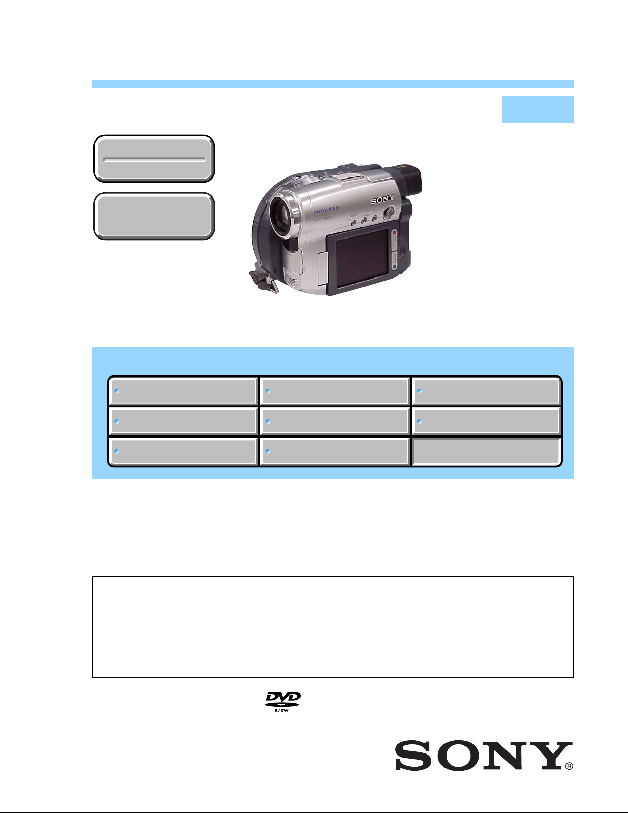
DCR-DVD201/DVD201E
RMT-835
DCR-DVD201
US Model
Canadian Model
Korea Model
Japanese Model
DCR-DVD201E
AEP Model
UK Model
East European Model
Australian Model
Chinese Model
Hong Kong Model
DCR-DVD201
DVD201E
E Model
Tourist Model
Ver 1.0 2004. 02
DIGITAL VIDEO CAMERA RECORDER
Photo : DCR-DVD201
On the MD-104 board and VC-354 board
This service manual provides the information that is premised the circuit board replacement service and not intended repair
inside the MD-104 board and VC-354 board.
Therefore, schematic diagram, printed wiring board, waveforms, mounted parts location and electrical parts list of the
MD-104
board and VC-354
board are not shown.
The following pages are not shown.
Disassembly...................................... Page 2-10
Schematic diagram ........................... Pages 4-31 to 4-82
Printed wiring board.......................... Pages 4-97 to 4-104
Mounted parts location .........................
Pages 4-106 to 4-108
Exploded views....................................Pages 5-10 to 5-11
Electrical parts list................................Pages 5-17 to 5-30

— 2 —
DCR-DVD201/DVD201E
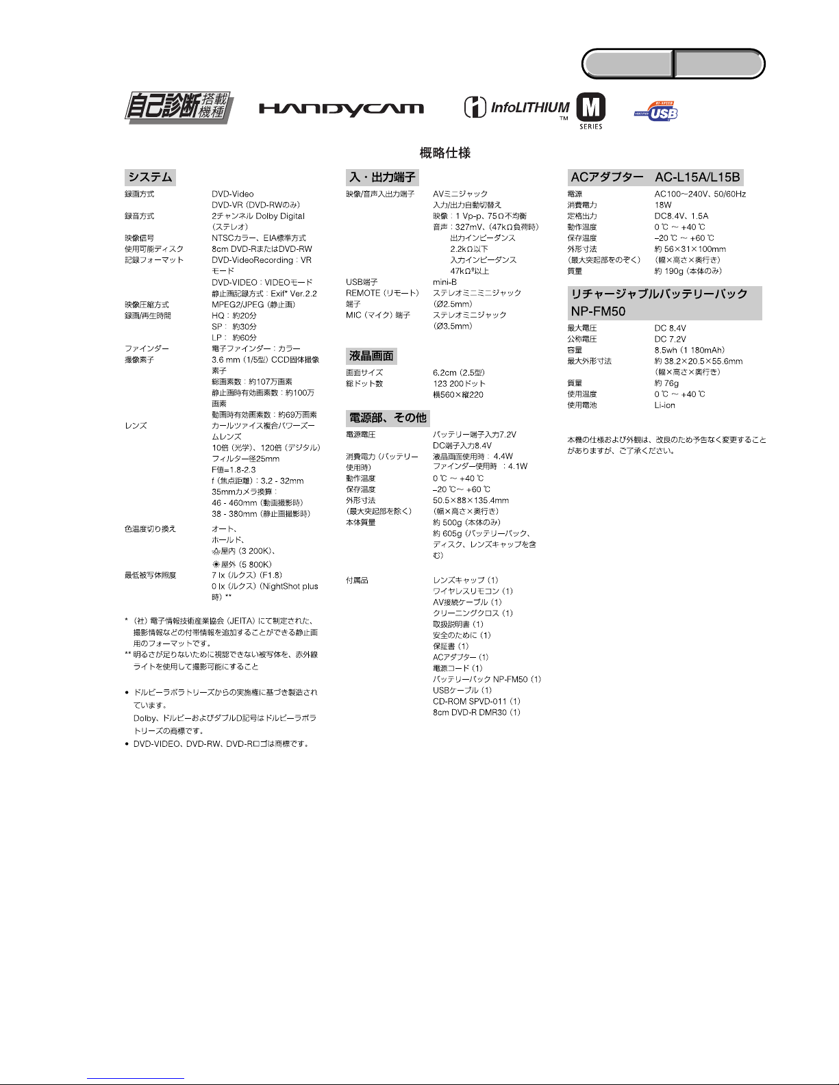
SPECIFICATIONS
ENGLISH JAPANESE
ENGLISH JAPANESE
Video camera
recorder
System
Video recording format
DVD-Video
DVD-VR (DVD-RW only)
Audio recording system
2ch Dolby* Digital
Video signal
Usable discs
8 cm DVD-R and DVD-RW
Video compression format
MPEG2/JPEG (Still images)
Recording/playback time
HQ: Approx. 20 minutes
SP: Approx. 30 minutes
LP: Approx. 60 minutes
Viewfinder
Electric viewfinder (color)
Image device
3.6 mm (1/5 type) CCD (Charge
Coupled Device)
Number of Pixels
Gross: Approx. 1 070 000 pixels
Effective (for still images ):
Approx. 1 000 000 pixels
Effective (for movies):
Approx. 690 000 pixels
Lens
Carl Zeiss
Combined power zoom lens
Filter diameter:
25 mm (1 in.)
10× (Optical), 120× (Digital)
F = 1.8 – 2.3
Focal length
3.2 – 32 mm (5/32 – 1 5/16 in.)
When converted to a 35 mm still
camera
For movies:
46 – 460 mm (1 7/8 – 18 1/8 in.)
For still images:
38 – 380 mm (1 1/2 – 15 in.)
Color temperature
Auto, HOLD (Hold), nIndoor
(3 200 K),
Outdoor (5 800 K)
Minimum illumination
7 lx (lux) (F 1.8)
0 lx (lux) (in the NightShot Plus
mode)*
* Objects unable to be seen due to
the dark can be shot with
infrared lighting.
Input/Output connectors
AUDIO/VIDEO input/output
AV MINI JACK,
input/output autoswitch
Video : 1 Vp-p, 75 Ω (ohms),
unbalanced
Audio : 327 mV, (at output
impedance of more than 47 kΩ
(kilohms))
Output impedance of less than
2.2 kΩ (kilohms)
Input impedance of more than
47 kΩ (kilohms)
USB jack
mini-B
REMOTE jack
Stereo mini-minijack (ø 2.5 mm)
MIC jack
Stereo minijack (ø 3.5 mm)
LCD display
Picture
6.2 cm (2.5 type)
Total number of pixels
123 200 (560 × 220)
General
Power requirements
7.2 V (battery pack)
8.4 V (AC adaptor)
Average power consumption
(when using the battery pack)
During camera recording using
LCD : 4.4 W
Viewfinder : 4.1 W
Operating temperature
0°C to 40°C (32°F to 104°F)
Storage temperature
–20°C to + 60°C
(–4°F to + 140°F)
Dimensions (Approx.)
50.5 × 88 × 135.4 mm
(2 1/4 × 3 1/2 × 5 3/8 in.)
(w/h/d)
Mass (approx.)
DCR-DVD201:
DCR-DVD201E:
605 g (15 oz)
including the battery pack,
disc and lens cap
Supplied accessories
See page 4.
* Manufactured under license
from Dolby Laboratories.
“Dolby” and the double-D
symbol are trademarks of Dolby
Laboratories.
AC adaptor
AC-L15A/L15B
Power requirements
100 – 240 V AC, 50/60 Hz
Current consumption
0.35 – 0.18 A
Power consumption
18 W
Output voltage
DC OUT: 8.4 V, 1.5 A in the
operating mode
Operating temperature
0°C to 40°C (32°F to 104°F)
Storage temperature
–20°C to + 60°C (–4°F to + 140°F)
Dimensions (approx.)
56 × 31 × 100 mm
4 in.) (w/h/d)
excluding projecting parts
Mass (approx.)
190 g (6.7 oz)
excluding power cord
Rechargeable
battery pack
NP-FM50
Maximum output voltage
DC 8.4 V
Output voltage
DC 7.2 V
Capacity
8.5 Wh (1 180 mAh)
Dimensions (approx.)
38.2 × 20.5 × 55.6 mm
(1 9/16 × 13/16 × 2 1/4 in.)
(w/h/d)
Mass (approx.)
76 g (2.7 oz)
Operating temperature
0°C to 40°C (32°F to 104°F)
Type
Lithium ion
Design and specifications are
subject to change without notice.
NTSC color, EIA standards
DCR-DVD201:
PAL color, CCIR standards
DCR-DVD201E:
50.5 × 88 × 136 mm
(w/h/d)
500 g
main unit only
(2 1/4 × 1 1/4 ×
— 3 —
DCR-DVD201/DVD201E
ENGLISH JAPANESE
ENGLISH JAPANESE
— 4 —
DCR-DVD201/DVD201E
1. Check the area of your repair for unsoldered or poorly-soldered
connections. Check the entire board surface for solder splashes
and bridges.
2. Check the interboard wiring to ensure that no wires are
"pinched" or contact high-wattage resistors.
3. Look for unauthorized replacement parts, particularly
transistors, that were installed during a previous repair . Point
them out to the customer and recommend their replacement.
4. Look for parts which, through functioning, show obvious signs
of deterioration. Point them out to the customer and
recommend their replacement.
5. Check the B+ voltage to see it is at the values specified.
6. Flexible Circuit Board Repairing
• Keep the temperature of the soldering iron around 270˚C
during repairing.
• Do not touch the soldering iron on the same conductor of the
circuit board (within 3 times).
• Be careful not to apply force on the conductor when soldering
or unsoldering.
Unleaded solder
Boards requiring use of unleaded solder are printed with the leadfree mark (LF) indicating the solder contains no lead.
(Caution: Some printed circuit boards may not come printed with
the lead free mark due to their particular size.)
: LEAD FREE MARK
Unleaded solder has the following characteristics.
• Unleaded solder melts at a temperature about 40°C higher than
ordinary solder.
Ordinary soldering irons can be used but the iron tip has to be
applied to the solder joint for a slightly longer time.
Soldering irons using a temperature regulator should be set to
about 350°C.
Caution: The printed pattern (copper foil) may peel away if the
heated tip is applied for too long, so be careful!
• Strong viscosity
Unleaded solder is more viscous (sticky , less pr one to flo w) than
ordinary solder so use caution not to let solder bridges occur such
as on IC pins, etc.
• Usable with ordinary solder
It is best to use only unleaded solder but unleaded solder may
also be added to ordinary solder.
SAFETY CHECK-OUT
After correcting the original service problem, perform the following
safety checks before releasing the set to the customer.
SAFETY-RELATED COMPONENT WARNING!!
COMPONENTS IDENTIFIED BY MARK 0 OR DOTTED LINE WITH
MARK 0 ON THE SCHEMATIC DIAGRAMS AND IN THE PARTS
LIST ARE CRITICAL TO SAFE OPERATION. REPLACE THESE
COMPONENTS WITH SONY PARTS WHOSE PART NUMBERS
APPEAR AS SHOWN IN THIS MANUAL OR IN SUPPLEMENTS
PUBLISHED BY SONY .
ATTENTION AU COMPOSANT AYANT RAPPORT
À LA SÉCURITÉ!
LES COMPOSANTS IDENTIFÉS P AR UNE MARQUE 0 SUR LES
DIAGRAMMES SCHÉMA TIQUES ET LA LISTE DES PIÈCES SONT
CRITIQUES POUR LA SÉCURITÉ DE FONCTIONNEMENT. NE
REMPLACER CES COMPOSANTS QUE PAR DES PIÈSES SONY
DONT LES NUMÉROS SONT DONNÉS DANS CE MANUEL OU
DANS LES SUPPÉMENTS PUBLIÉS PAR SONY.
CAUTION :
Danger of explosion if battery is incorrectly replaced.
Replace only with the same or equivalent type.
ENGLISH JAPANESE
ENGLISH JAPANESE
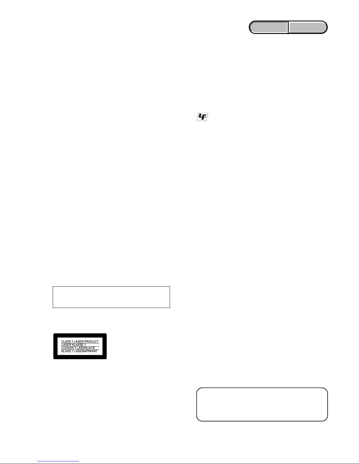
WARNING!!
WHEN SERVICING, DO NOT APPRO ACH THE LASER
EXIT WITH THE EYE TOO CLOSELY. IN CASE IT IS
NECESSARY TO CONFIRM LASER BEAM EMISSION,
BE SURE TO OBSER VE FROM A DISTANCE OF MORE
THAN 30 cm FROM THE SURFACE OF THE
OBJECTIVE LENS ON THE OPTICAL PICK-UP BLOCK.
CAUTION:
The use of optical instrument with this product will increase eye
hazard.
CAUTION
Use of controls or adjustments or performance
procedures other than those specified herein may
result in hazardous radiation exposure.

— 5 —
DCR-DVD201/DVD201E
ENGLISH JAPANESE
ENGLISH JAPANESE

— 6 —
DCR-DVD201/DVD201E
TABLE OF CONTENTS
1. SERVICE NOTE
1-1. SERVICE NOTE ·····························································1-1
1. NOTE FOR REPAIR ·······················································1-1
2. POWER SUPPLY DURING REPAIRS ·························· 1-2
3. TO TAKE OUT A CASSETTE WHEN NOT EJECT
(FORCE EJECT) ·····························································1-2
4. NOTES ON HANDLING THE OPTICAL PICK-UP ····1-2
5. PRECAUTION FOR CHECKING EMISSION
OF LASER DIODE························································· 1-2
1-2. SELF-DIAGNOSIS FUNCTION····································1-3
1. SELF-DIAGNOSIS FUNCTION····································1-3
2. SELF-DIAGNOSIS DISPLAY ······································· 1-3
3. SELF-DIAGNOSIS CODE TABLE································1-3
2. DISASSEMBLY
2-1. DISASSEMBLY······························································2-1
2-2. SERVICE POSITION ····················································· 2-5
2-3. CIRCUIT BOARDS LOCATION ···································2-8
2-4. FLEXIBLE BOARDS LOCATION ································2-9
Disassembling procedure of MD block assembly is
not shown. Page 2-10 is not shown.
HELP (List of caution points is shown here.)
3. BLOCK DIAGRAMS
3-1. OVERALL BLOCK DIAGRAM (1/4) ··························· 3-1
3-2. OVERALL BLOCK DIAGRAM (2/4) ··························· 3-3
3-3. OVERALL BLOCK DIAGRAM (3/4) ··························· 3-5
3-4. OVERALL BLOCK DIAGRAM (4/4) ··························· 3-7
3-5. POWER BLOCK DIAGRAM (1/3)································3-9
3-6. POWER BLOCK DIAGRAM (2/3)······························3-11
3-7. POWER BLOCK DIAGRAM (3/3)······························3-13
4. PRINTED WIRING BOARDS AND
SCHEMATIC DIAGRAMS
4-1. FRAME SCHEMATIC DIAGRAM (1/3)······················· 4-1
FRAME SCHEMATIC DIAGRAM (2/3)·······················4-3
FRAME SCHEMATIC DIAGRAM (3/3)·······················4-5
4-2. SCHEMATIC DIAGRAMS
• CD-504 (CCD IMAGER)
SCHEMATIC DIAGRAM ····························4-11
• FP-884 (LITHIUM BATTERY, SW)
SCHEMATIC DIAGRAM ····························4-13
• FP-887 (USB JACK) FLEXIBLE
SCHEMATIC DIAGRAM ····························4-15
• FP-890 (PANEL REV SW) FLEXIBLE
SCHEMATIC DIAGRAM ····························4-15
• FP-891 (EJECT MOTOR, SW) FLEXIBLE
SCHEMATIC DIAGRAM ····························4-17
• LB-107 (EVF I/F, BACK LIGHT)
SCHEMATIC DIAGRAM ····························4-17
• JS-030 (KEY I/F)
SCHEMATIC DIAGRAM ····························4-19
• MA-429 (MIC, REMOTE SENSOR, MULTI AV JACK)
SCHEMATIC DIAGRAM ····························4-21
• SE-143 (PITCH/YAW SENSOR)
SCHEMATIC DIAGRAM ····························4-23
• PD-220 (LCD DRIVE)
SCHEMATIC DIAGRAM ····························4-25
• CONTROL SWITCH BLOCK (BL8700, PS8700)
SCHEMATIC DIAGRAM ····························4-27
• CONTROL SWITCH BLOCK (SH8700)
SCHEMATIC DIAGRAM ····························4-29
Shematic diagram of the MD-104 board and VC-354
are not shown.
Pages from 4-31 to 4-82 are not shown.
4-3. PRINTED WIRING BOARDS
• CD-504 (CCD IMAGER)
PRINTED WIRING BOARD ·······················4-85
• FP-890 (PANEL REV SW)
PRINTED WIRING BOARD ·······················4-87
• FP-884 (LITHIUM BATTERY, SW) FLEXIBLE
PRINTED WIRING BOARD ·······················4-88
• JS-030 (KEY I/F)
PRINTED WIRING BOARD ·······················4-89
• MA-429 (MIC, REMOTE SENSOR, MULTI AV JACK)
PRINTED WIRING BOARD ·······················4-91
• PD-220 (LCD DRIVE)
PRINTED WIRING BOARD ·······················4-93
• LB-107 (EVF I/F, BACK LIGHT)
PRINTED WIRING BOARD ·······················4-95
• SE-143 (PITCH/YAW SENSOR)
PRINTED WIRING BOARD ·······················4-95
Printed wiring board of the MD-104 board and VC-354
are not shown.
Pages from 4-97 to 4-104 are not shown.
4-4. MOUNTED PARTS LOCATION ······························· 4-105
Mounted parts location of the MD-104 board and
VC-354 are not shown.
Pages from 4-106 to 4-108 are not shown.
5. REPAIR PARTS LIST
5-1. EXPLODED VIEWS ······················································ 5-3
5-1-1.OVERALL SECTION·····················································5-3
5-1-2.CABINET (R) SECTION ··············································· 5-4
5-1-3.LCD SECTION ······························································· 5-5
5-1-4.EVF SECTION································································5-6
5-1-5.LENS SECTION ····························································· 5-7
5-1-6.CABINET (L) SECTION················································5-8
5-1-7.D LID SECTION·····························································5-9
Exploded view and parts list of MD BLOCK are not
shown. Pages 5-10 and 5-11 are not shown.
Checking supplied accessories. ····································· 5-12
5-2. ELECTRICAL PARTS LIST ········································5-14
Electrical parts list of the MD-104 board and
VC-354 board are not shown.
Pages from 5-17 to 5-30 are not shown.
1-1
SECTION 1
SERVICE NOTE
DCR-DVD201/DVD201E
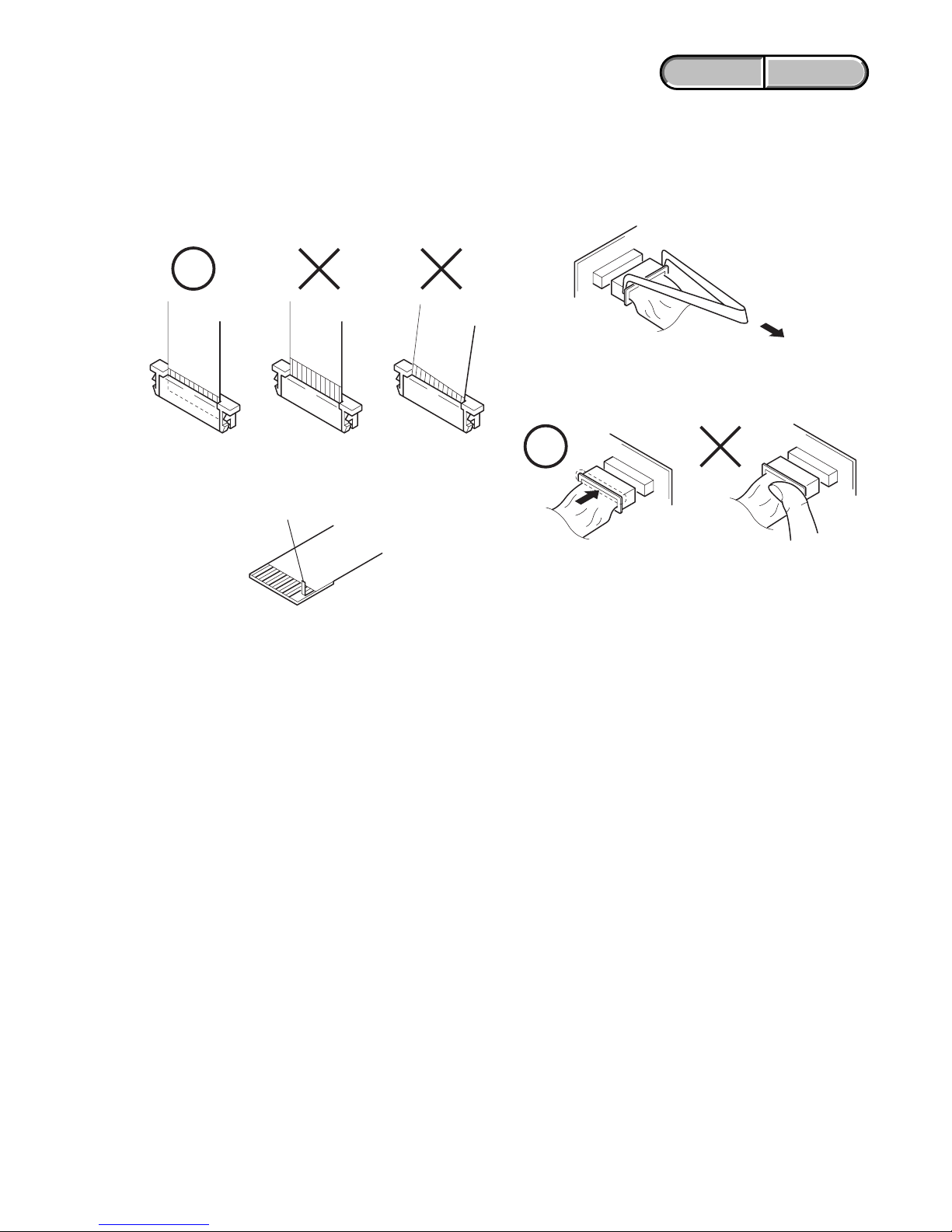
Make sure that the flat cable and flexible board are not cracked of
bent at the terminal.
Do not insert the cable insufficiently nor crookedly.
Cut and remove the part of gilt
which comes off at the point.
(Take care that there are
some pieces of gilt left inside)
When remove a connector, don't pull at wire of connector.
Be in danger of the snapping of a wire.
When installing a connector, don't press down at wire of connector.
Be in danger of the snapping of a wire.
1-1. SERVICE NOTE
1. NOTE FOR REPAIR
ENGLISH JAPANESE
ENGLISH JAPANESE
1-2
DCR-DVD201/DVD201E
2. POWER SUPPLY DURING REPAIRS
In this unit, about 10 seconds after power is supplied to the battery terminal using the regulated power supply (8.4V), the po wer is shut off so
that the unit cannot operate.
This following two methods are available to prevent this. Take note of which to use during repairs.
Method 1.
Use the AC power adaptor.
Method 2.
Connect the servicing remote commander RM-95 (J-6082-053-B) to the LANC jack, and set the commander switch to the “ADJ” side.
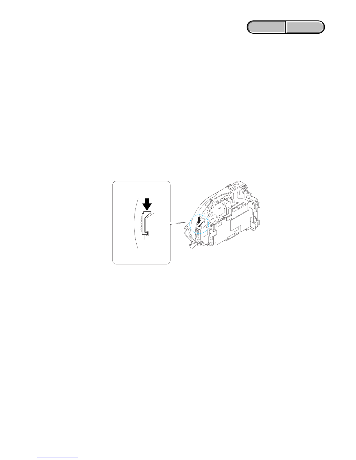
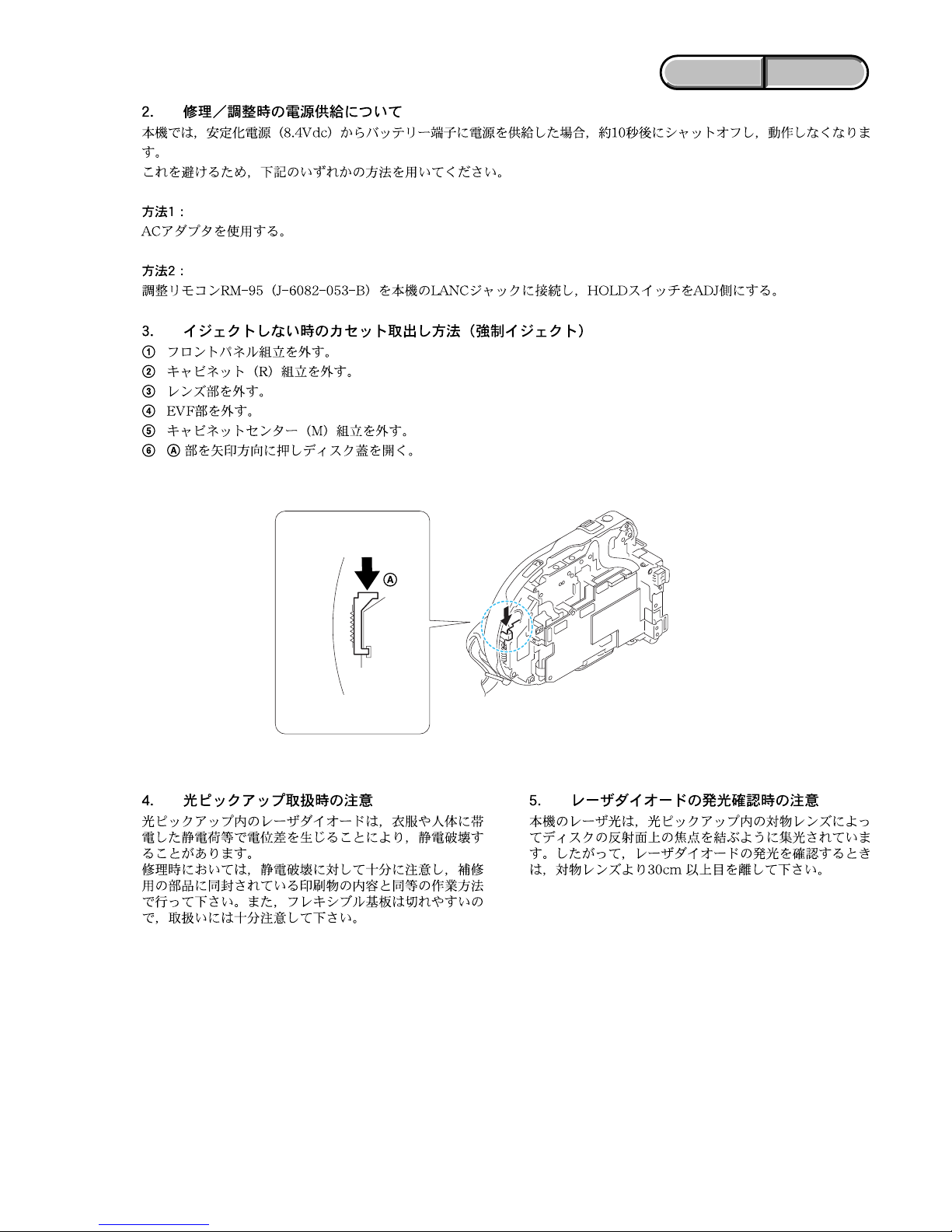
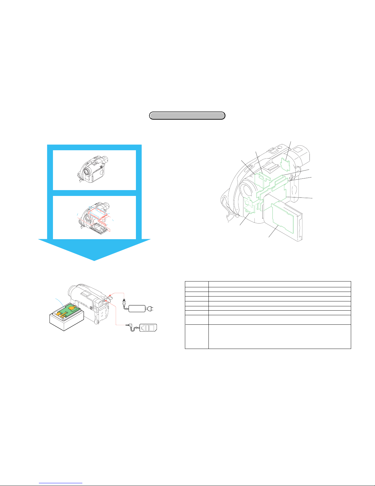
3. TO TAKE OUT A CASSETTE WHEN NOT EJECT (FORCE EJECT)
1 Remove the front panel assembly.
2 Remove the cabinet (R) assembly.
3 Remove the lens block.
4 Remove the EVF block.
5 Remove the cabinet center (M) assembly.
6 Push the portion A in the direction of the arrow and open the disc cover.
ENGLISH JAPANESE
ENGLISH JAPANESE
A
4.
NOTES ON HANDLING THE OPTICAL PICK-UP
The laser diode may suffer electrostatic breakdown because of the
potential difference generated by the charged electrostatic load, etc.
on clothing and the human body.
During repair, pay attention to electrostatic breakdown and also use
the procedure in the printed matter which is included in the repair
parts.
The flexible board is easily damaged and should be handled with
care.
5. PRECAUTION FOR CHECKING EMISSION OF
LASER DIODE
Laser light of the equipment is focused by the object lens in the
optical pick-up so that the light focuses on the reflection surface of
the disc. Therefore, be sure to keep your eyes more then 30 cm
apart from the object lens when you check the emission of laser
diode.
1-3
DCR-DVD201/DVD201E
ENGLISH JAPANESE
ENGLISH JAPANESE
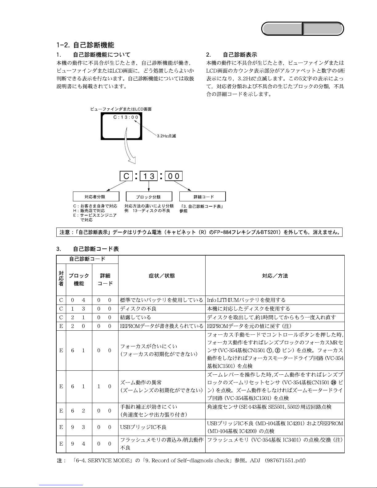
1-2. SELF-DIAGNOSIS FUNCTION
1. SELF-DIAGNOSIS FUNCTION
When problems occur while the unit is operating, the self-diagnosis
function starts working, and displays on the viewfinder, or LCD
screen what to do. This function consists of two display; selfdiagnosis display and service mode display.
Details of the self-diagnosis functions are provided in the Instruction
manual.
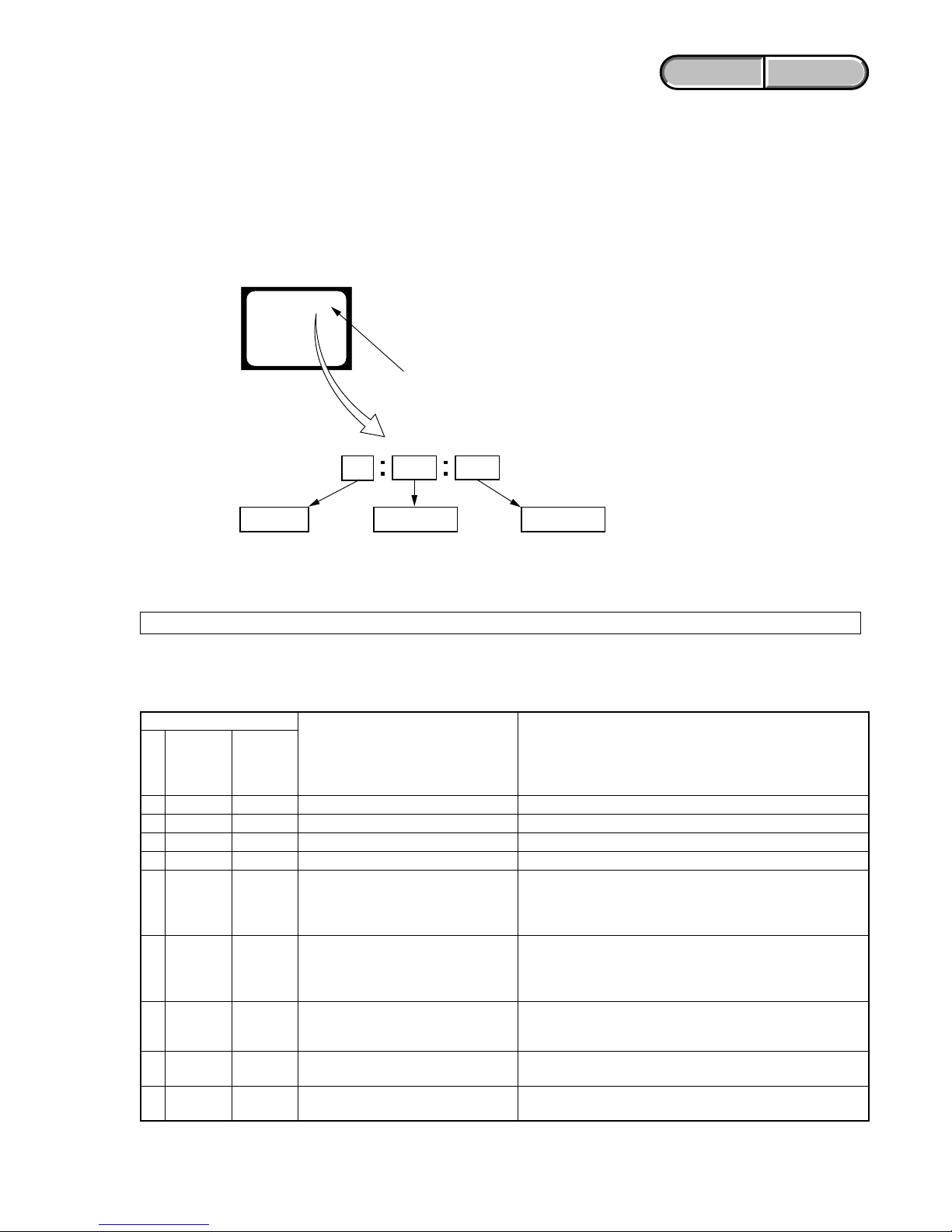
2. SELF-DIAGNOSIS DISPLAY
When problems occur while the unit is operating, the counter of the
viewfinder or LCD screen consists of an alphabet and 4-digit number ,
which blinks at 3.2Hz. This 5-character display indicates the
“repaired by:”, “block” in which the problem occurred, and “detailed
code” of the problem.
Note: The “self-diagnosis display” data will be kept even if the lithium battery (FP-884 flexible board BT5201 of the cabinet (R) assembly) is removed.
0 0
1 3C
Repaired by:
Self-diagnosis Code Table.
Indicates the appropriate
step to be taken.
E.g.
13....Faulty disc is used.
Block
Detailed Code
Blinks at 3.2Hz
C : Corrected by customer
H : Corrected by dealer
E : Corrected by service
engineer
Viewfinder or LCD screen
C : 1 3 : 0 0
3. SELF-DIAGNOSIS CODE TABLE
C
C
C
E
E
E
E
E
E
Block
Function
04
13
21
20
61
61
62
93
94
Detailed
Code
00
00
00
00
00
10
00
00
01
Symptom/State
Non-standard battery is used.
Faulty disc is used.
Condensation.
EEPROM data are rewritten.
Difficult to adjust focus
(Cannot initialize focus.)
Zoom operations fault
(Cannot initialize zoom lens.)
Handshake correction function does not
work well. (With pitch angular velocity
sensor output stopped.)
USB bridge IC fault
Fault of writing to or erasing the flash
memory
Self-diagnosis Code
Repaired by:
Correction
Use the InfoLITHIUM battery.
Use a compatible disc with the camcorder.
Remove the disc, and insert it again after one hour.
Make EEPROM data correct value. (Note)
Inspect the lens block focus MR sensor (Pin 1, 2 of CN1501 of
VC-354 board) when focusing is performed when the control button
is pressed in the focus manual mode and inspect the focus motor drive
circuit (IC1501 of VC-354 board) when the focusing is not perf ormed.
Inspect the lens block zoom reset sensor (Pin wh of CN1501 of
VC-354 board) when zooming is performed when the zoom switch
is pressed and inspect the zoom motor drive circuit (IC1501 of
VC-354 board) when the zooming is not performed.
Inspect angular velocity sensors (SE5501, 5502 of SE-143
board) peripheral circuits.
Inspect the USB bridge IC (MD-104 board IC4201) and EEPROM
(MD-104 board IC4200)
Inspect the flash memory (VC-354 board IC3401) (Note)
Note: Refer to “9. Record of Self-diagnosis check” of “6-3. SERVICE
MODE”, ADJ (987671551.pdf).
1-4
DCR-DVD201/DVD201E
ENGLISH JAPANESE
ENGLISH JAPANESE
SECTION 1
SERVICE NOTE
1-5
DCR-DVD201/DVD201E
ENGLISH JAPANESE
ENGLISH JAPANESE
1-6E
DCR-DVD201/DVD201E
ENGLISH JAPANESE
ENGLISH JAPANESE
DCR-DVD201/DVD201E
2-1 2-2
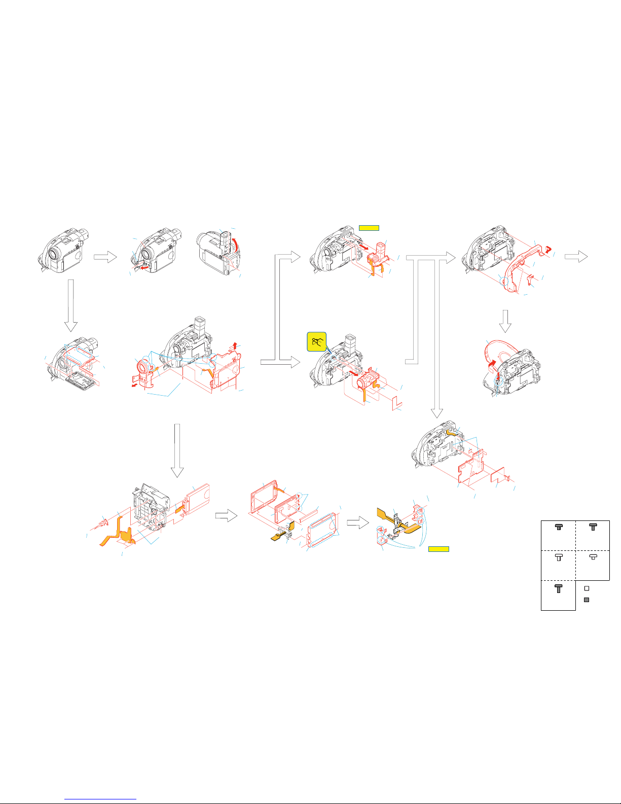
2-1. DISASSEMBLY
The following flow chart shows the disassembly procedure.
VC-354
1
2
4
3
2
1
3
5
6
7
9
5
1
Two grip screws (M1.7x3) black
2
Two grip screws (M1.7x3) black
3
Six claws
4
P cabinet (C) assembly
5
Sheet (MY)
1
Open the jack cover
2
EG grip Screw (M1.7x4) black
3
EG grip Screw (M1.7x4) black
4
Turn over the EVF section in the
direction of the arrow.
5
EG grip Screw (M1.7x4) black
6
Two EG grip Screws (M1.7x4) black
7
Three EG grip Screws (M1.7x4) black
8
Two EG grip Screws (M1.7x4) black
9
Five claws
0
Remove the cabinet (R) section
in the direction of the arrow.
qa
MA-429 board (27P)
qs
F panel section
qd
FP-884 flexible board (33P)
qf
Cabinet (R) section
1
Two grip screws (M1.7x3) black
2
Two grip screws (M1.7x3) black
3
Six claws
4
P cabinet (C) assembly
5
FP-890 board (22P)
6
Hinge (87) assembly, Hinge cover (O),
Hinge cover (U), FP-890 board
1
Tape (0915)
2
Three screws (M1.7x2.5) silver
3
FP-892 flexible board (39P)
4
From lens flexible board (29P)
5
Lens section
1
Screw (M1.7x2.5) silver
2
VC heat sink, VC radiation sheet,
VC insulating sheet
3
Three screws (M1.7x2.5) silver
4
Control switch block (PS8700) (20P)
5
Board to board (CN1007, CN4901) (100P)
6
Radiation sheet (135)
7
VC-354 board
1
Screw (M1.7x2.5) silver
2
EG grip screw (M1.7x4) black
3
FP-883 flexible board (10P)
4
FP-889 flexible board (20P)
5
EVF section
1
Grip screw (M1.7x3) black
2
Four claws
3
Hinge cover (O)
4
Hinge cover (U)
5
Hinge (87) assembly, FP-890 board
7
Sheet (MY)
8
Screw (M1.7x5) black
9
Control switch block (BL8700) (6P)
0
Two claws
qa
P cabinet (M) assembly
qs
PD-220 board, Insulating sheet,
Light guide plate block
qa
qf
qd
0
4
qs
A
A
B
B
B
B
B
B
B
B
2
1
D
3
7
D
1
4
5
2
5
8
5
4
3
1
7
9
qa
2
0
6
qs
HELP 02
HELP 01
2
3
1
A
A
E
A
4
5
D
3
4
4
3
1
2
5
D
8
See page
2-3.
Screw
M1.7x3
3-084-817-21
Screw
M1.7x2.5
3-078-889-11
Silver
Black
Screw
M1.7x4
3-087-376-01
Tapping screw
M1.7x3.5
3-078-890-01
Tapping screw
M1.7x5
3-081-204-21
A
C
B
D
E
6
1
2
1
Screw (M1.7x2.5) silver
2
Front fixed plate
3
EG grip screw (M1.7x4) black
4
Screw (M1.7x2.5) silver
5
Two tapping screws (M1.7x5) black
6
Claw
7
Remove the cabinet center (M)
assembly in the direction of the arrow.
1
Push this portion with a finger
in the direction of the arrow a.
2
Open the D lid assembly
in the direction of the arrow b.
3
4
5
2
6
B
1
7
D
E
D
1
5
4
2
3
6
1
Two tapping screws (M1.7x3.5) silver
2
Speaker retainer plate assembly
3
Three tapping screws (M1.7x3.5) silver
4
FP-890 board (20P)
5
FP-884 flexible board (8P)
6
Three EG grip screws (M1.7x4) black
7
LCD section
C
C
B
B
7
a
b
SECTION 2
DISASSEMBLY
2. DISASSEMBLY
2. DISASSEMBLY
DCR-DVD201/DVD201E
2-3 2-4
VC-354
VC-354
MD-104
MD-104
1
Screw (M1.7x2.5) silver
2
VC heat sink, VC radiation sheet,
VC insulating sheet
3
Screw (M1.7x2.5) silver
4
Claw
5
Screw (M1.7x2.5) silver
Screw
M1.7x3
3-084-817-21
Screw
M1.7x2.5
3-078-889-11
Silver
Black
Screw
M1.7x4
3-087-376-01
Tapping screw
M1.7x3.5
3-078-890-01
Tapping screw
M1.7x5
3-081-204-21
A
E
E
D
D
C
7
2
56
3
1
8
1
E
1
2
C
2
3
1
4
C
2
1
3
4
2
4
B
B
8
6
qa
5
3
0
4
D
D
D
1
C
B
D
E
7
3
HELP 03
9
2
1
Three screws (M1.7x2.5) silver
2
Board to board (CN1007,CN4901) (100P)
3
Radiation sheet (135)
4
VC-354 board
1
Screw (M1.7x2.5) silver
2
VM heat sink, VM radiation sheet, VM insulating sheet
3
Tripod large
4
Sheet radiation (2345)
1
Two screws (M1.7x2.5) silver
2
Screw (M1.7x2.5) silver
3
Three tapping screws (M1.7x5) black
4
Tapping screw (M1.7x3.5) silver
1
Two tapping screws (M1.7x5) black
2
D blind plate assembly
1
Two tapping screws (M1.7x5) black
2
Tapping screw (M1.7x3.5) silver
3
Control switch block (PS8700)
1
Remove the grip belt
in the direction of the arrow.
2
Two tapping screw (M1.7x3.5) silver
3
Grip belt sheet metal (Rear)
4
Grip belt
1
Open the jack cover (DC) in the directions of the arrows a and b.
2
DC-IN connector inlet
3
Harness (DM-144), FP-228 flexible board (Dew senser)
4
Control switch block (PS8700)
D
1
D
1
3
4
4
3
2
3
1
Remove the grip belt
in the direction of the arrow a.
2
Push this portion with a finger
in the direction of the arrow b.
3
Open the D lid assembly
in the direction of the arrow c.
5
DC-IN connector inlet (3P)
6
Harness (DM-144) (2P) (Dew sensor)
7
FP-891 flexible board (10P)
8
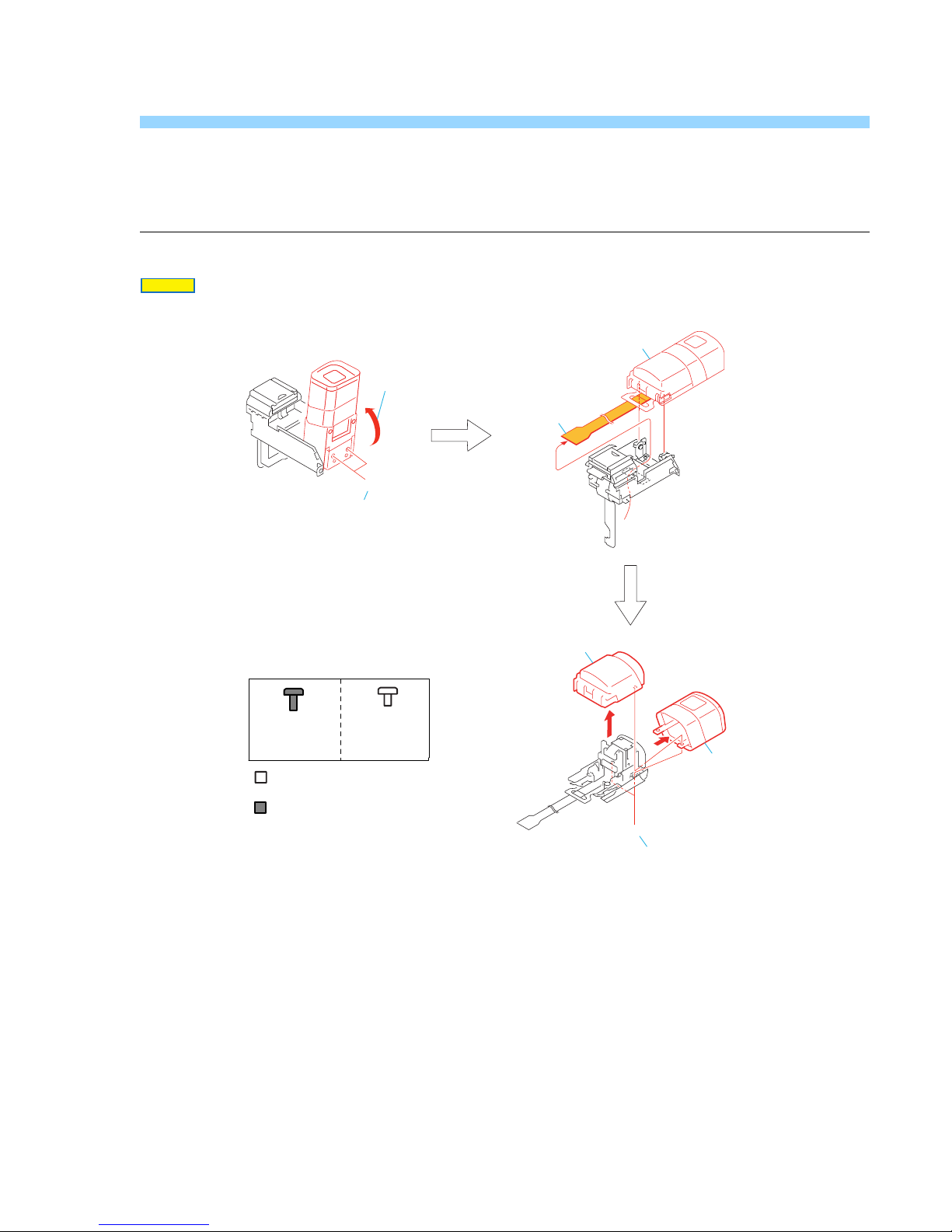
Remove the MD block assembly in the
direction of the arrow.
6
Two EG grip screws (M1.7x4) black
7
Control switch block (PS8700) (20P)
8
Battery terminal board (3P)
9
Battery terminal board
0
FP-887 flexible board (8P)
qa
Square type connector (USB 5P),
FP-887 flexible board
2
a
c
b
2
1
E
1
2
1
Two tapping screws (M1.7x5) black
2
Remove the D lid assembly
in the direction of the arrow.
Optical pickup
Caution
Precautions during handling
Refer to level 3
Disassembling procedure of
MD block assembly.
Be sure to place the DVD drive with its
optical pickup facing upward.
Do not touch the optical pickup surface.
(J-2501-162-A)
Use the adjustable wrist strap (J-2501-162-A) as the
preventive measure for static electricity when the
removing and installing the MD black assembly because
the MD black assembly of this mechanism beck is easily
affected by the static electricity.
ab
DCR-DVD201/DVD201E
2. DISASSEMBLY
2. DISASSEMBLY
2-5 2-6
2-2. SERVICE POSITION
VC-354
VC-354
Control switch block
(PS8700) (20P)
Monitor TV
Extension cable (100P)
(J-6082-352-A)
AC power
adaptor
AC IN
Adjustment remote
commander (RM-95)
LANC
DC-IN
CN1006
CN1007
CN1001
CN4901
VC-354 board
MD-104 board
MA-429 board
MD-104
VC-354
[SERVICE POSITION TO CHECK THE DVD DRIVE SECTION]
Connection to Check the DVD drive section
To check the DVD drive section, set the DVD drive to PLAY mode. (Set the mode dial to PLAY position,
or set forced PLAY mode by using the adjustment remote commander.)
Operate the DVD drive using the adjustment remote commander (with the HOLD switch set in the OFF position).
Note: Removing the control switch block (PS8700) means removing the LID OPEN switch. Therefore the DVD
drive section will not move even if the forced PLAY mode is set up.
Setting the forced PLAY mode
1) Select page: 0, address: 01, and set data: 01.
2) Select page: 0, address: 10, and set data: 00.
3) Select page: D, address: 10, set data: 02, and press the
PAUSE button of the adjustment remote commander.
Exiting the forced PLAY mode
1) Select page: 0, address: 01, and set data: 01.
2) Select page: 0, address: 10, and set data: 00.
3)
Select page: D, address: 10, set data: 00, and press the
PAUSE button of the adjustment remote commander.
4) Select page: 0, address: 01, and set data: 00.
CN4902
AUDIO/
VIDEO jack
2
1
3
B
B
5
6
4
B
B
3
4
5
2
6
B
1
7
D
E
D
D
1
4
3
2
B
2
1
5
D
3
4
4
3
1
2
5
D
CPC-8 jig
(J-6082-388-A)
7
9
qa
qf
qd
0
qs
B
B
B
8
B
B
8
6
qa
5
3
0
4
D
D
D
1
7
9
2
2. DISASSEMBLY
2. DISASSEMBLY
DCR-DVD201/DVD201E
2-7 2-8
PD-220
PD-220 board
AC power
adaptor
AC I
N
Adjustment remote
commander (RM-95)
[PD-220 BOARD SERVICE POSITION]
LANC
1
2
4
3
5
A
A
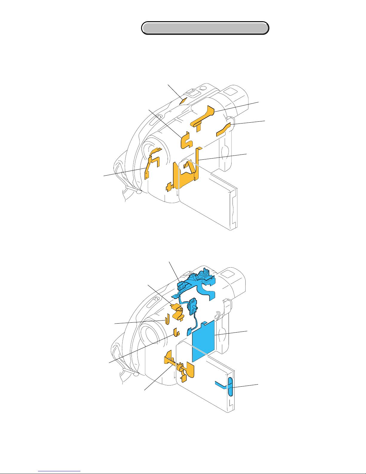
2-3. CIRCUIT BOARDS LOCATION
VC-354
JS-030
MD-104
SE-143
CD-504
MA-429
PD-220
LB-107
CD-504
JS-030
PD-220
LB-107
MA-429
SE-143
MD-104
NAME
FUNCTION
VC-354
CCD IMAGER
KEY I/F
LCD DRIVE
EVF I/F, BACKLIGHT
MIC, REMOTE SENSOR, MULTI AV JACK
PITCH/YAW SENSOR
RF PROCESS, DVD DSP, MECHA DRIVE, MICRO COMPUTER, FLASH, LATCH, USB I/F,
SHOCK SENSOR, CONNECTOR, DC/DC CONVERTER
A/D CONV., TIMING GENERATOR, CAMERA PROCESS, LENS DRIVE,
DVD SYSTEM CONTROL, 128M SDRAM, 16M FCRAM, DVD CODEC,
64M SDRAM, VIDEO IN/OUT, VIDEO A/D CONVERTER, EVF DRIVE, CAMERA CONTROL,
HI CONTROL, HI/ DIGITAL STILL CONTROL, 32M FLASH MEMORY, AUDIO I/O, MIC AMP,
PITCH/YAW SENSOR AMP, CONNECTOR, DD CONNECTOR
2-9E
DCR-DVD201/DV201E
2. DISASSEMBLY
2. DISASSEMBLY
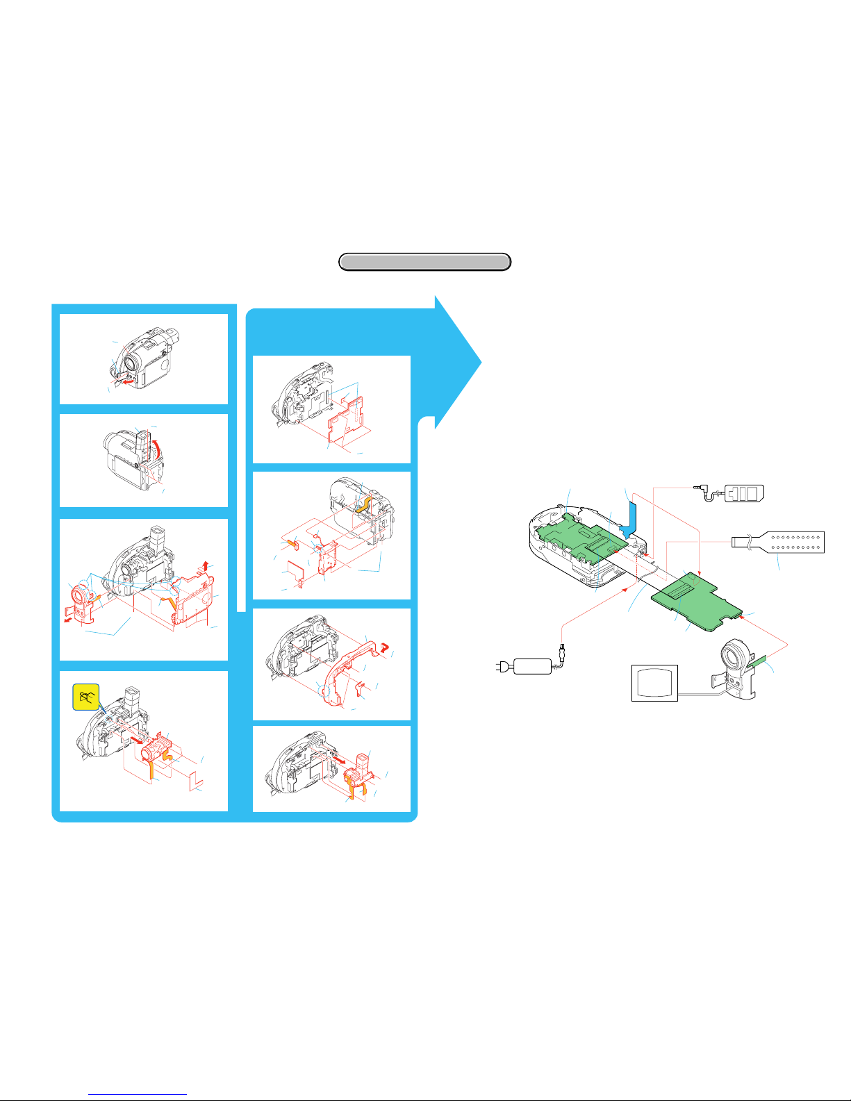
2-4. FLEXIBLE BOARDS LOCATION
The flexible boards contained in the lens block is not shown.
FP-887
FP-884
CONTROL SWTICH BLOCK (PS8700)
CONTROL SWTICH
BLOCK (SH8700)
CONTROL SWTICH
BLOCK (BL8700)
FP-889
FP-892
FP-228
FP-891
FP-888
FP-890
FP-883
FP-629

Disassembling procedure of MD bloc k
assembly are not shown.
Page 2-10 is not shown.
DCR-DVD201/DVD201E
HELP
HELP
Sheet attachment positions and procedures of processing the flexible boards/harnesses are shown.
2
1
6
C
D
A
B
5
7
3
4
E
F
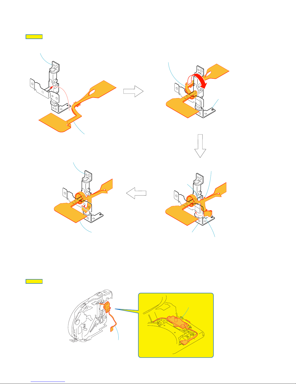
HELP 01
1
Turn over the EVF seiction
in the direction of the arrow
A
.
2
Two screws (M1.7x5) black
3
EVF seiction
4
Remove the FP-889 flexible board
in the direction of the arrow
B
.
5
Two screws (M1.7x5) black
6
Remove the VF lens assembly in the direction of the arrow C.
7
Remove the VF cabinet (Upper) in the direction of the arrow D.
Silver
Black
Screw
M1.4x2.5
3-084-681-01
F
Tapping screw
M1.7x5
3-081-204-21
E
DCR-DVD201/DVD201E
HELP
Control switch block
(PS8700)
Control switch block
(PS8700)
HELP 02
HELP 03
1
FP-890 board
2
Hinge (87) assembly
Hinge (87) assembly
FP-890 board
3
Twist the FP-890
flexible board.
Hinge (87) assembly
Hinge (87) assembly
5
Attach the adhesive surface.
Adhesive surface
4
When installing FP-890
flexible board insert it in
the groove.

DCR-DVD201/DVD201E
Link
Link
3. BLOCK DIAGRAMS
POWER BLOCK DIAGRAM (1/3)
POWER BLOCK DIAGRAM (2/3)
POWER BLOCK DIAGRAM (3/3)
OVERALL BLOCK DIAGRAM (4/4)
OVERALL BLOCK DIAGRAM (3/4)
OVERALL BLOCK DIAGRAM (2/4)
OVERALL BLOCK DIAGRAM (1/4)
POWER BLOCK DIAGRAM (1/3)
POWER BLOCK DIAGRAM (2/3)
POWER BLOCK DIAGRAM (3/3)
OVERALL BLOCK DIAGRAM (4/4)
OVERALL BLOCK DIAGRAM (3/4)
OVERALL BLOCK DIAGRAM (2/4)
OVERALL BLOCK DIAGRAM (1/4)
DCR-DVD201/DVD201E
3. BLOCK DIAGRAMS
3. BLOCK DIAGRAMS
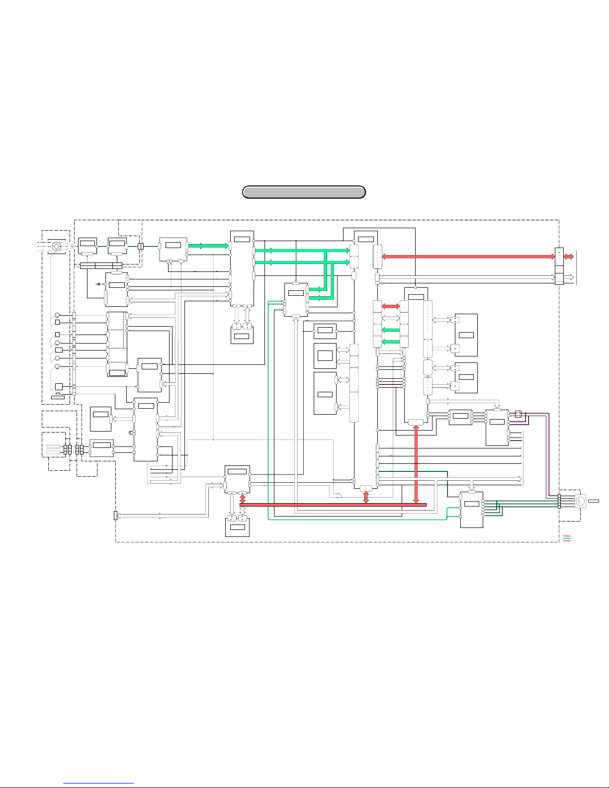
3-1. OVERALL BLOCK DIAGRAM (1/4)
3-1 3-2
SECTION 3
BLOCK DIAGRAMS
( ) : Number in parenthesis ( ) indicates the division number of schematic diagram where the component is located.
49
46
8
10
IC3203(1/2)
DIGITAL
STILL
CONTROL
IC3401
FLASH MEMORY
32M bit
10
25 163829 36
45
62 92 60 39
X3002
20MHz
IC1603
CH SO,SCK
16
20
ZOOM MOTOR
DRIVE
XRST
18
IC1601
I DRIVE
+,-
I HALL
+,-
135
11
ND HALL
+,-
ND DRIVE
+,-
CCD OUT
+,-
V1-V4
RG,H2
71
23
73
10
FMR A,B
ZMRST SENS
78
75
77
65
63
66
70
67
69
TIMING
GENERATOR
FOCUS MOTOR
DRIVE
ZOOM
MOTOR
PRE
DRIVE
183
9
18
22
CD-504 BOARD(1/2) FP-892
FLEXIBLE
(1/2)
21
EXT STROBO
EXT STROBO
25
IC1501
ND
FILTER
DRIVE
IRIS DRIVE
VC-354 BOARD(1/3)
2
12
IC1101
LENS ASSY
M
IC3001
18
PITCH AD
YAW/PITCH
8
H
H
MR
IRIS
(SHUTTER)
SENSOR
YAW AD
AMP
129
YAW SENSOR
PITCH SENSOR
SE5501
11
SE5502
M
M
FOCUS
MOTOR
1-4 14 • 18
SE-143
BOARD
CD-504
BOARD(2/2)
FP-888
FLEXIBLE
FP-892
FLEXIBLE
(2/2)
CAMERA CONTROL
ZOOM
MOTOR
M
CN1501
CCD
IMAGER
NIGHT SHOT
ZOOM
RESET
SENSOR
ND FILTER
METER
ZOOM VR AD
130
3
CN1601CN5101
CN5101
CN1601
37363
4
1
54
187
TO
OVERALL
BLOCK DIAGRAM
(4/4)
(PAGE 3-8)
AGC
A/D CONV.
IC5100
53
5
2
1
5
6
4
22
23
20
9
10
12
72
67
32
17
25
X1601
66MHz(DVD201)
54MHz(DVD201E)
CAM SO,SI,SCK
XSYS RST
XSYS RST
CHCK CHCK
SPCK
SPCK
HD,VD,FLD HD,VD,FLD
47
48
12
1
CLPOBCLPOB
CH SO,SCK
XNS SW
(1/18)
(1/18)
FOCUS +,-
ZOOM +,-
ZOOM A,XA
ZOOM B,XB
DIR1B
EN1
DIR1A
(3/18)
(3/18)
(2/18)
(13/18)
(11/18)
IC3004
EEPROM
(11/18)
IC1502
(16/18)
CN1601CN5206
CN5100
CN5101
4
2
352
3
44 45
92
91
90
1
16
CN1008
FOR
ADJUSTMENTS
•
XSHD,XSHP,CLPDM
5
4
S/H
IMAGER
IC5101
•
30
31
•
••
38
37
XLK RST
XSYS RST
IC1804
64Mbit
SDRAM
(5/18)
IC3603
16Mbit
FCRAM
(4/18)
IC3502
AUDIO
PLL
(15/18)
IC2302
D/A CONV.
A/D CONV.
(7/18)
IC3803
64Mbit
SFRAM(1)
(7/18)
IC3801
64Mbit
SDRAM(0)
(15/18)
IC2301
AUDIO
I/O
(5/18)
IC3601
MS BS
MS DIO
MS SCLK
XLK RST
IFI HD
IFI VD
IFI OE
Y OUT
C OUT
XRST VTR
IFI HD
IFI VD
IFI OE
71
|
56
128
140
42
213
53
213
|
215
29
20 26
35
1
2
13
12
15
17
9
6
26
C5
B6
C10
B11
H1
J1
7
187
13
12
15
CAMERA
PROCESS
A1-A22
SCLK27
S XRST S XRST
XSYS RST
C XRST
D0-D15
195 174
D0-D15A0-A13
(14/18)
13 14 1
38 33 64
IC1803
(2/18)
DVD
SYSTEM
CONTROL
IC3501
(4/18)
DVD
CODEC
IC3701
(6/18)
77
43 109
B27
137
102
8
K12
H11
161 148
AD0-AD13
CAM SO,SI,SCK
AD0-AD13
AD0-AD13
16-19 29 21
24-21 11 19 32 31 25
8 9 15
66
4
2
3
SO, SI, SCK
1 48
MS BS
MS DIO
MS SCLK
HI SO,SI,SCK
AF5 AG3
AD5 AF3
AG4 AD6
AF4 AD7
AG5
AG6
AD9
AF6
AD8
AG7
AC12
AF7
N23
T26
T27
M24
U26
P23
U27
R26
T1
R2
T4
T2
U4
U1
U2
V1
AC13AC14
AD11-AD18
AF9-AF19
AG10-AG20
AD19-AD21
AD23
AF20-AF23
AG21-AG24
D23
B22
B24
B26
107
42
|
27
20
|
1
D15
|
D0
A11
|
A0
SDATA31
|
SDATA0
SADRS11
|
SADRS0
SED15
|
SED0
SEA20
|
SEA1
D15
|
D0
A19
|
A0
W4 V4
Y1 U4
Y2 W5
W1 T2
W2 T4
V1 U5
V2 R2
U1 V5
IC3602
128Mbit
SDRAM
AF8
AG8
AG9
AD10
(9/18)
IC2001
VIDEO
A/D
CONV.
31 68
52
|
59
42
|
49
34
115
199
208
|
6
|
9
11
12
13
A3-A7
B5-B9
D6-D9
E10E9
E13
D19
A21
B21
J24
H27
B23
N26
D7
A2
L2
K1
A5
D8
9
12
8
A4
R5
15
3
16
2
19
25
17
23
D4
B2
E4
AB2
AA2
AB1
H4
G4
E1
G27
F26
H24
AF2
AE2
AC2
AD2
AD1
J5
G2
VC0-VC7
B25
D27
F24
E27
F26
E24
P27
E26
H4
D1
G2
E1
F2
K4
E2
H2
VDIN0-VDIN7
G24
F27
P26
G26
H24
G27
H26
K26
F1
J4
G1
L4
H1
K2
J1
M4
VDIO0-VDIO7
L26
J27
K24
K27
M23
L27
M26
M27
M2
J2
N4
M1
N2
N1
P4
P2
SD0-SD7
SO 0, SI 0, XSCK 0
HD
ADCK
S VDCK0
SAD0
BCK
C ADIO
PANEL R
PANEL G
PANEL B
C VDCK0
XSYS RST
C XRST
C ADO
VSP SO X,XVSP SCK X
L
R
L
R
L
R
R
L
C ADIO
BCK
AE27
51
33
34
37 44
AF1-AF6
AG2-AG4
W1
W4
Y1
Y2
Y4
AA1
AA2
AA4
AB1
AB2
AC1
AC2
AC4
AD1
AD2
AD4
AD5
AD7
AD9
AE1
AG6
AG7
62
129
90
62
129
90
AD6
AG5
AG8
AD10
AF7
AC8
AF8
AD11
AG10
AG9
AF9
51
33
34
37 44
AG24
AF24
AF25
AD22
AG25
AD23
AB24
AF27
AE26
AF26
AA23
AD13-AD21
AF12-AF23
AG14-AG23
AF13
AG26
G26
J24
DATA0 31
|
DATA0 0
D31
|
D0
A10
|
A0
D31
|
D0
A10
|
A0
ADRSO 10
|
ADRSO 0
DATA1 31
|
DATA1 0
ADRS1 10
|
ADRS1 0
15 14
55
54
53
51
(8/18)
IC2101
VIDEO
IN/OUT
AGC
ACC
PANEL R
PANEL G
PANEL B
SP+
SP-
MIC L
MIC R
EVF R
EVF G
EVF B
Y OUT
C OUT
Y OUT
PANEL XHD
PANEL XVD
46
7
34
18
14
22
39
48
42
36
910
VIDEO/AUDIO
CN5501
MA-429
BOARD(1/3)
13
11
9
15
18
9
5
10
1
6
41
76
21
37
36
38
IFI HD
IFI VD
IFI OE
AFCK
SCLK27
CLK24
IFI C0-IFI C7
IFI Y0-IFI Y7
IFI Y0-IFI Y7
IFI C0-C3
IFI Y0-IFI Y7
SPCK
IFI C0-IFI C7
64 6366
6
2
C OUT
Y
C
V
Y
C
V
V27
P24
W26
T23
W27
R24
Y26
U23
Y27
AA26
T24
AA27
AB26
V23
AB27
U24
HD0-HD15
V27
P24
W26
T23
W27
R24
Y26
U23
Y27
AA26
T24
AA27
AB26
V23
AB27
U24
HA0-HA2
XATA REST
HD0-HD15
HA0-HA2
XATA REST
V24
AD26
W24
73
84 86
88
90
92
94
96
75 82
95
97
98
61
TO
OVERALL
BLOCK DIAGRAM
(3/4)
(MD-104)
2
(PAGE 3-5)
TO
OVERALL
BLOCK DIAGRAM
(2/4)
(PAGE 3-3)
3
11
47
9
L2 L1
K1 M5
K2 M4
T5 U2
R4 T1
R1 R5
P2 P1
N2 P4
N1 N4
M1 M2
PANEL XHD
PANEL XVD
EVF R
EVF G
EVF B
YOUT
COUT
XRST VTR XRST VTR
DO LK-D15 LK DO LK-D15 LK
VD SO,SI,SCK VD SO,SI,SCK
VD SO,SI,SCK
F4
E4
D1
CN1007
CN1006
A23-A26
C27
D21-D27 F24
B23-B26
D0 LK-D15 LK
AUDIO SIGNAL
VIDEO SIGNAL
VIDEO/AUDIO SIGNAL
|
K2
L2
B1
C4
F3
E3
G3
F1
K6
L4
M9
J9
K9
L9
H12
J11
K11
16
17
15
 Loading...