

Page 1
Page 2
B4W~
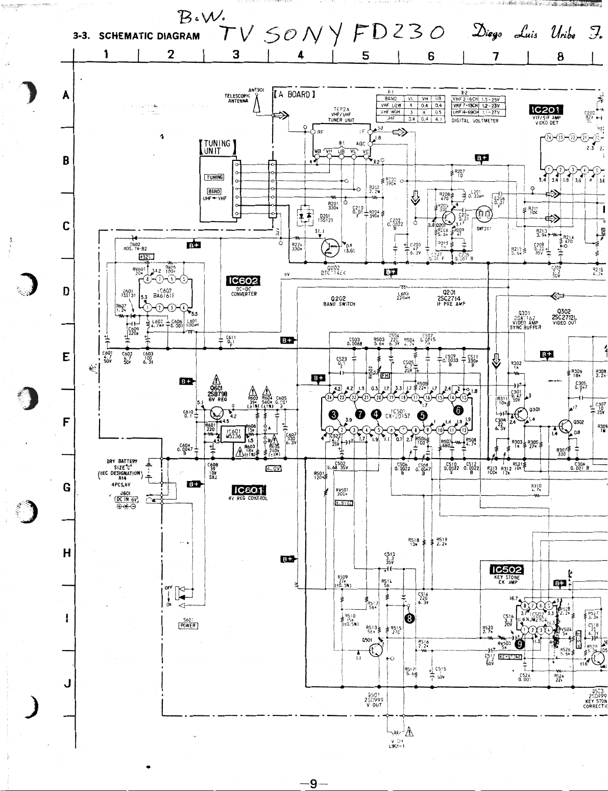
3-3. SCHEMATIC DIAGRAM
T V 5 [) N YFD 2 3 O
J.
"1 A
1
,.).
..
..
".'.
..
"'
( ..
~
B
e
o
E
F
1 2 3 I 4 I 5 I 6
..
~
1
I
TUN1NGI
~
UHf"-VHI='
o-I-----t<+.
r------------,
I
i
ROS
" -
B2
i
I
I
c'601
C602
4. ,
SO,
C603
100
6.3V
4. ,
SOY
.-
":":
I
I
.
Eh
• I
¡ 6n602
nAA·~'"
oc-oc
CONVfRTER
I
C611
0.1
,
J
~
!
:-5V
___
Q202
~:..<.
____~_______
Q202
BANO SWITCH
T.'--------------l--
r
L_
.
_______
Q201
25C2714
IF PRE
_
A¡;'P
8
+
_______
......
:
it-,!'
-----<C~----
c.pJl
,_0V
_____
LL
0302
2SC2712L
VtOEO
~21S
'_·._,
OuT
R306
1ek
J30:',
1
¡,F~I'}~:
I
·_
.
RlOe
2.2.(
A30~
1111
:
:
)
G
H
J
Qó
L
Ol
2S0999
V
OUT
7~3~~9
KEY
STON
CORREC
TI(
---------------¡-:r:----------------
l
~.,
c
&
l/ i) 1
L~Ol-
,
•
-9--
Page 3

•
AII
capacitors
50WV
and
tantalums.
•
Al!
reslstors
specified.
• % indicares
• c::::J:
Power
•
supply
Voltage
•
under
no
mark:
•
Voltages
VolTage variatlons
tion
tolerances.
• Waveforms are
Voltage
tion
toleranees.
•
Crded
• Slgnal
~
Q>
Or
less are
are
adjustment
voltage
from
external
and
no-signal
TV
are
taken
variations
nl,imbers
path.
:AUDIO
:VIDEO
are
is
waveforms are
taken
in
)lF unless
not
ind.cated
in
íl
and
J
..
> W
tolerance.
for
repair.
dc
6V
and
fed
power
voltage
be
noted
be
noted
10
waveforP1s.
de
conditions.
with a VOM I1npvt I
may
with a oseilloscopl
may
reter
otherwl
exce~
or
les
with
jacI
with
due
due
I
1"-----
..
• I I I
ckr
FLEXIBLE]
[
I
BOARD
.
I
Note:
The
eomponents
by
mark
fied
ted
line
are
critical
Replaee
number
specifieQ.
TUNING
StE~
5101-2
with
for
only
identl-
&.
or
mark
safety.
with
UNIT
.
II
SIOl
ISANul
VHF
. "
UHF
ThIS
(
os 1he
T801 FLYBACK TRANSFORMER
RIOI
¡-
'--(
~YIOI
...
0102
.r:;.·c>::il
L.::.:.:-"
RIOl
unl!
15
oS.8Mb
SCHEMATIC OIAGRAM
Note:
Les
dot-
une
&.
pOllr
Ne les
part
piece
fié.
0101
RI02
RIO.
.,
RIOS
~
~
suppllad
lad b loc.k
composar
marque,
la
séeur;'
rempl¡
portant
Wll
VH
\lB
,.....
'f1..
ve
32V
Gl/D
)
•.
r
H"'''P
+36 V
9---4t--
----¡-
 Loading...