

Page 1
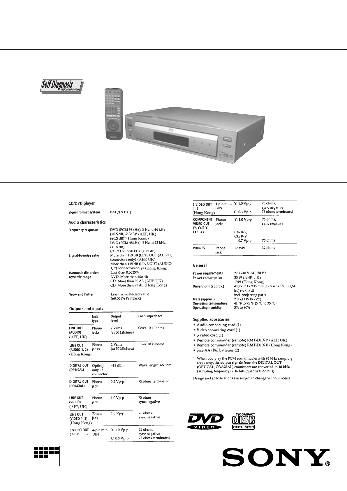
DVP-S7700
RMT-D107E/D107P
SERVICE MANUAL
SPECIFICATIONS
AEP Model
Hong K ong Model
UK Model
MICROFILM
CD/DVD PLAYER
Page 2
SAFETY CHECK-OUT
WARNING!!
WHEN SERVICING, DO NO T APPR O A CH THE LASER
EXIT WITH THE EYE TOO CLOSELY. IN CASE IT IS
NECESSARY TO CONFIRM LASER BEAM EMISSION,
BE SURE TO OBSERVE FROM A DISTANCE OF
MORE THAN 25 cm FROM THE SURFACE OF THE
OBJECTIVE LENS ON THE OPTICAL PICK-UP BLOCK.
CAUTION:
The use of optical instrument with this product will increase eye
hazard.
CAUTION
Use of controls or adjustments or performance of procedures
other than those specified herein may result in hazardous radiation exposure.
CLASS 3B LASER
LUOKAN 3B LASER
LASERKLASS 3B
SAFETY CHECK-OUT
After correcting the original service problem, perform the following
safety checks before releasing the set to the customer:
1. Check the area of your repair for unsoldered or poorly-soldered connections. Check the entire board surface for solder
splashes and bridges.
2. Check the interboard wiring to ensure that no wires are
“pinched” or contact high-wattage resistors.
3. Look for unauthorized replacement parts, particularly transistors, that were installed during a previous repair. Point them
out to the customer and recommend their replacement.
SAFETY-RELATED COMPONENT WARNING!!
COMPONENTS IDENTIFIED BY MARK ! OR DOTTED
LINE WITH MARK ! ON THE SCHEMA TIC DIAGRAMS
AND IN THE PARTS LIST ARE CRITICAL TO SAFE
OPERATION. REPLACE THESE COMPONENTS WITH
SONY PARTS WHOSE PART NUMBERS APPEAR AS
SHOWN IN THIS MANUAL OR IN SUPPLEMENTS PUBLISHED BY SONY.
4. Look for parts which, though functioning, show obvious signs
of deterioration. Point them out to the customer and recommend their replacement.
5. Check the B+ voltage to see it is at the values specified.
– 2 –
Page 3

TABLE OF CONTENTS
Section Title Page Section Title Page
Service Note ............................................................................ 4
1. GENERAL
This Player Can Play the Following Discs .................... 1-1
Getting Started .............................................................. 1-1
Basic Operations ........................................................... 1-2
Playing Discs in Various Modes .................................... 1-4
Setting and Adjustments ............................................... 1-9
Additional Information ................................................... 1-10
2. DISASSEMBLY
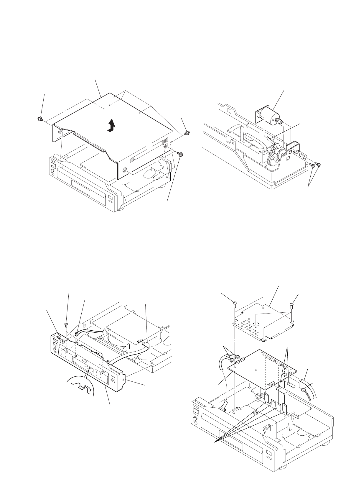
2-1. Upper Case Removal.................................................... 2-1
2-2. Front Panel Removal .................................................... 2-1
2-3. Door Open/Close Motor Removal................................. 2-1
2-4. MB-84 Board Removal.................................................. 2-1
2-5. AU-218 Board Removal ................................................ 2-2
2-6. MD Block Ass’y Removal .............................................. 2-2
2-7. TK-47 Board Removal................................................... 2-2
2-8. Tray Removal ................................................................ 2-2
2-9. Skew Motor (M903) Removal ....................................... 2-3
2-10. Sled Motor (M501) Removal ......................................... 2-3
2-11. Spindle Motor (M901) Removal .................................... 2-3
2-12. Optical Pick-up Removal............................................... 2-3
2-13. Internal Views ................................................................ 2-4
2-14. Circuit Boards Location ................................................. 2-5
3. BLOCK DIAGRAMS
3-1. Overall Block Diagram .................................................. 3 -1
3-2. RF/Servo Block Diagram .............................................. 3-3
3-3. Signal Process Block Diagram ..................................... 3-5
3-4. Video Block Diagram..................................................... 3-7
3-5. System Control Block Diagram ..................................... 3-9
3-6. Audio Block Diagram..................................................... 3-11
3-7. Mode Control Block Diagram ........................................ 3-13
3-8. Power Block Diagram.................................................... 3-15
4. PRINTED WIRING BOARDS AND SCHEMATIC
DIAGRAMS
4-1. Frame Schematic Diagram ........................................... 4-3
4-2. Printed Wiring Boards and Schematic Diagrams ......... 4-7
TK-47 Printed Wiring Board .......................................... 4-7
TK-47 (RF, Servo 1) Schematic Diagram ..................... 4-11
TK-47 (RF, Servo 2) Schematic Diagram ..................... 4-13
MB-84, FG-43 Printed Wiring Boards........................... 4-15
MB-84 (AV Decoder) Schematic Diagram .................... 4-19
MB-84 (Clock Generator) Schematic Diagram............. 4-21
MB-84 (DNR) Schematic Diagram................................ 4-23
MB-84 (Video Encoder) Schematic Diagram................ 4-25
MB-84 (Drive 1) Schematic Diagram ............................ 4-27
MB-84 (Drive 2), FG-43 Schematic Diagrams.............. 4-29
MB-84 (DSP 1) Schematic Diagram ............................. 4-31
MB-84 (DSP 2) Schematic Diagram ............................. 4-33
MB-84 (Bias) Schematic Diagram ................................ 4-35
MB-84 (IF µ-com) Schematic Diagram ......................... 4-37
MB-84 (L Gate Array) Schematic Diagram ................... 4-39
MB-84 (ARP, Decrypt) Schematic Diagram .................. 4-41
MB-84 (System µ-com) Schematic Diagram ................ 4-43
MB-84 (S Gate Array) Schematic Diagram .................. 4-45
AU-218 Printed Wiring Board ....................................... 4-47
AU-218 (Audio 1) Schematic Diagram ......................... 4-51
AU-218 (Audio 2) Schematic Diagram ......................... 4-53
AU-218 (Video Buffer) Schematic Diagram.................. 4-55
YS-19 Printed Wiring Board and
Schematic Diagram ....................................................... 4-57
ER-8 Printed Wiring Board............................................ 4-59
ER-8 (EURO AV 1) Schematic Diagram ....................... 4-63
ER-8 (EURO AV 2) Schematic Diagram ....................... 4-65
ER-8 (EURO AV 3) Schematic Diagram ....................... 4-67
HP-120 Printed Wiring Board and
Schematic Diagram ....................................................... 4-69
FP-75 Printed Wiring Board .......................................... 4-71
FP-75 Schematic Diagram............................................ 4-73
CN-113, DR-88, FL-108, FR-160, PW-120
Printed Wiring Boards ................................................... 4-75
CN-113, DR-88, FL-108, FR-160, PW-120
Schematic Diagrams ..................................................... 4-77
PS-421 Printed Wiring Board........................................ 4-79
PS-421 Schematic Diagram.......................................... 4-81
POWER BLOCK (HS-930SH) Printed Wiring Board.... 4-83
POWER BLOCK (HS-930SH) Schematic Diagram...... 4-85
5. IC PIN FUNCTION DESCRIPTION
5-1. Interface Control Pin Function (MB-84 Board IC604) .. 5-1
5-2 System Control Pin Function (MB-84 Board IC805) .... 5-2
6. TEST MODE
6-1. Starting up Test Mode ................................................... 6-1
6-2. Selection of Check Item ................................................ 6-1
6-2-1. Selected Item Check ................................................ 6-1
6-2-2. All Items Check ........................................................ 6-1
6-3. Error Display.................................................................. 6-2
6-4. General Description of Checking Method..................... 6-2
6-5. Drive Auto Adjustment .................................................. 6-8
6-6. Drive Manual Operation ................................................ 6-12
6-6-1. Drive Manual Operation Menu Screen .................... 6-12
6-6-2. Disc T ype.................................................................. 6-12
6-6-3. Manual Control 1...................................................... 6-12
6-6-4. Manual Control 2...................................................... 6-13
6-6-5. Manual Control 3...................................................... 6-13
6-6-6. Manual Adjust 1 ....................................................... 6-13
6-6-7. Manual Adjust 2 ....................................................... 6-14
6-6-8. Auto Adjust ............................................................... 6-14
6-6-9. Check ....................................................................... 6-14
6-6-10. EEPROM Data Screen Display................................ 6-15
6-7. Other Operation............................................................. 6-15
6-8. Emergency History ........................................................ 6-16
6-9. Error Code ..................................................................... 6-18
7. ELECTRICAL ADJUSTMENT
7-1. Power Supply Check ..................................................... 7-1
1. HS-930SH Board........................................................... 7-1
7-2. Adjustment of System Control ...................................... 7-2
1. System Clock 27 MHz Adjustment ................................ 7-2
7-3. Adjustment of Video System......................................... 7-2
1. Video Level Adjustment ................................................ 7-2
2. S-terminal Output Check............................................... 7-2
3. Checking Component Video Output B-Y...................... 7-2
4. Checking Component Video Output R-Y...................... 7-3
5. Checking Component Video Output Y .......................... 7-3
6. Checking RGB Output R............................................... 7-3
7. Checking RGB Output G ............................................... 7-3
8. Checking RGB Output B............................................... 7-4
9. Checking S Video Output S-C ...................................... 7-4
10. Checking S Video Output DC Level.............................. 7-4
7-4. Adjustment Related Parts Arrangement ....................... 7-6
8. REPAIR PARTS LIST
8-1. Exploded Views ............................................................. 8-1
8-1-1. Case Assembly ........................................................ 8-1
8-1-2. Front Panel Assembly .............................................. 8-2
8-1-3. Chassis Assembly.................................................... 8-3
8-1-4. DVD Mechanism Chassis Assembly (1) .................. 8-5
8-1-5. DVD Mechanism Chassis Assembly (2) .................. 8-6
8-2. Electrical Parts List........................................................ 8-7
– 3 –
Page 4
SERVICE NOTE
1. DISASSEMBLY
• This set can be disassembled in the order shown below.
Set
Upper Case
(Page 2-1)
MB-84
Board
(Page 2-1)
MD Block
Ass’y
(Page 2-2)
Tray
(Page 2-2)
Optical
Pick-up
(Page 2-3)
Front Panel
Section
(Page 2-1)
Door Open/
Close Motor
(Page 2-1)
TK-47
Board
(Page 2-2)
Skew
Motor
(Page 2-3)
Spindle
Base
(Page 2-3)
Spindle
Motor
(Page 2-3)
AU-218
Board
(Page 2-2)
Sled
Motor
(Page 2-3)
– 4 –
Page 5
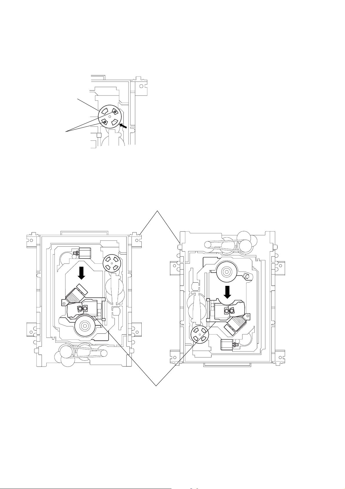
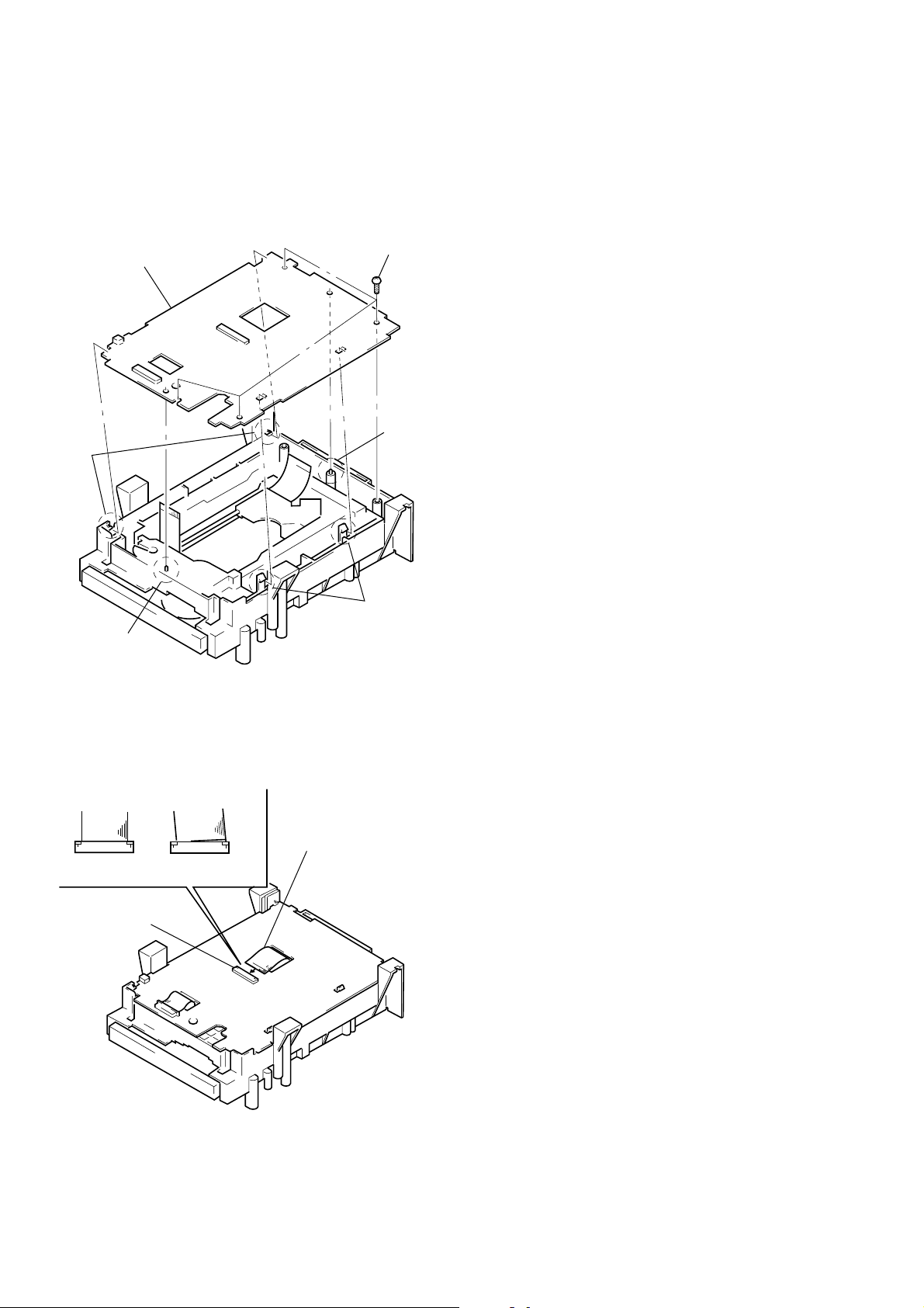
2. DISK REMOVAL PROCEDURE
(at POWER OFF)
2-1. How to Open the Door
1) With the top case removed, rotate the gear (D) 1 in direction
A to open the door. (See Fig. 1)
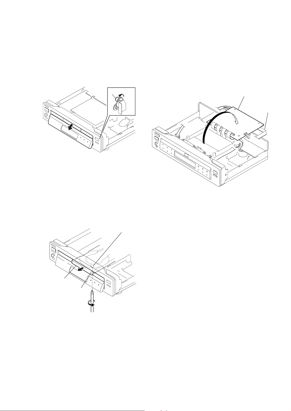
3. HOW TO SER VICE MB-84 (SIDE B) BO ARD
1) Remove the case from the set. (Refer to 2-1)
2) Remove the cover (upper). (Refer to 2-3)
3) Set the MB-84 board as shown in Fig. 3.
Note 1: Do not disconnect wiring.
Note 2: Spread a insulating material under the MB-84 board
and through down lest you should short.
4) Mount the extention cable (J-6090-079-A).
(MB-84 (CN601) ↔ FL-107 (CN153))
1 Gear (D)
A
Fig. 1
2-2. How to Draw out Tray
1) Insert a cross-tip screwdriver into a hole at the bottom, and
rotate the cam gear 2 in direction B. (See Fig. 2)
Note: To prevent a damage of cam g ear, rotate it in direction
B by 1/4 turn.
2) Draw out the tray 3 in direction C by hand, and remove a
disk. (See Fig. 2)
2 Cam gear
MB-84 board
Extention Cable
(J-6090-079-A)
Fig. 3
3 Tray
C
Hole
B
Fig. 2
– 5 –
Page 6
4. NOTE ON MOUNTEING SLED MOTOR
1) Push the sled motor ass’y 1 toward direction A. (See Fig. 4)
2) Tighten two screws 2 (M1.7 × 2.5).
1 Sled motor ass’y
A
2 Two screws (M1.7 × 2.5)
Fig. 4
3) Raising the MD block ass’y 3 90 º with the side down.
confirm that the optical pick-up 4 falls by self weight.
(See Fig. 5)
4) Further, with the front side of MD block ass’y 3 up, confirm
that the optical pick-up falls by self weight.
3 MD block ass’y
Upper
Lower Front side
4 Optical pick-up
Upper
Lower
Front side
Fig. 5
– 6 –
Page 7
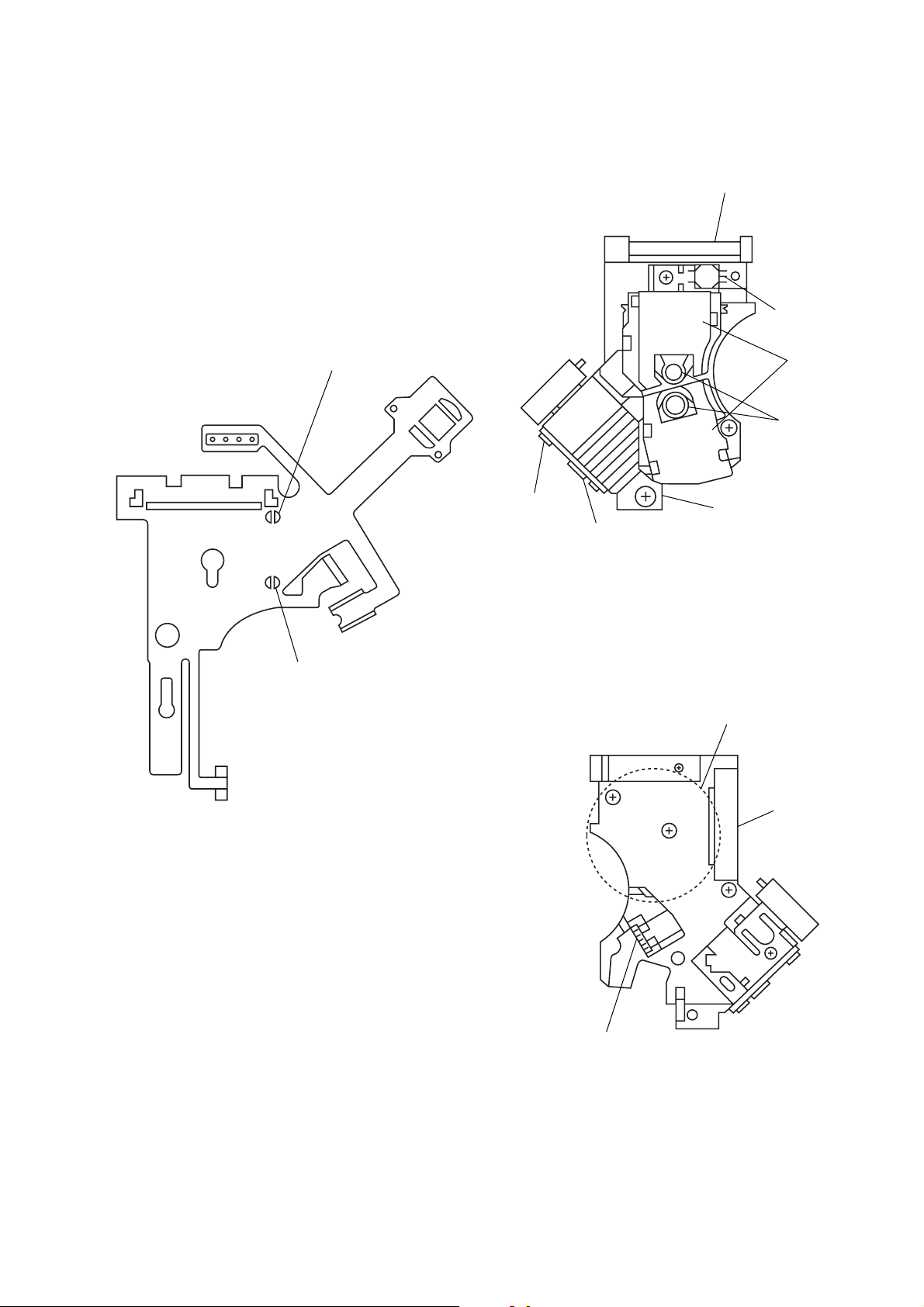
5. REPLACING OPTICAL PICK-UP
Slide base bearing
Skew sensor
Lens actuator
covers
Objective lenses
U-shaped guide
OEIC
Laser holder
5-1. Handling
1) A red laser diode for DVD requires more attention to static
electricity than general infrared laser diodes for CD.
Because its durability to static electricity is far weaker than
that of infrared laser diodes, always use an earth band when
handling the optical pick-up block as service parts.
2) As for the flexible board KHS-180A (RP) packed as service
parts, the short lands have been soldered to protect from static
electricity. Accordingly, remove solders when replacing optical pick-up. (See Fig. 6)
DVD short land
CD short land
3) In handling the KHS-180A (RP), do not touch inhibited parts
shown in Fig. 7, but grip the slide base bearing and U-shaped
guide.
Touch inhibited parts
• Objective lens
• Skew sensor
• Laser holder
• Laser coupler
• Flexible board
• OEIC
• Lens actuator covers
Fig. 6 Flexible board
Flexible board
Connector
Laser coupler
Fig. 7 KHS-180A (RP)
– 7 –
Page 8
6. NOTE ON ASSEMBLING MECHANICAL DECK
6-1. Application of Grease
1) Grease must be applied if the following parts were replaced.
(See Fig. 8)
Note 1: Recommended grease is Foil KG-70MP.
Note 2: In applying grease, take care not to allow grease to
stick to other parts (particularly, rubber belt, spindle
motor, and optical pick-up)
Base unit holder
2 bosses
Slide base Skew cam
Tray 3 grooves
Note:Add grease if tray
moves slowly.
Cam gear
Loading pulley shaft
Note:Add grease if tray
generates noise
periodically.
Fig. 8
– 8 –
Page 9
6-2. Cleaning Spindle Motor Turntable
1) Remove the tray. (Refer to 2-7)
2) Clean the spindle motor turntable if disc antiskid rubber (black)
is dirty. (See Fig. 9)
6-4. Deformation of Insulator
1) Assemble the spindle base into the base unit.
2) Loc k with 4 shoulder screws. (See Fig. 11)
3) Chec k if 4 insulators deformed. (See Fig. 11)
Spindle motor
Turntable
Fig. 9
6-3. Aligning Phase of Cam Gear and
Drive Gear
1) Align triangle marks when assembling the cam gear and drive
gear. (See Fig. 10)
Four step screws
Two insulators
Insulator
Two insulators
Good NG
Fig. 11
6-5. Note on Mounting FG-43 Board
1) Align two bosses. (See Fig. 12)
2) Fix the board securely with screws (PTPWH2 × 5). (The sen-
sor will not function normally if the board floats up.)
Drive gear Cam gear
Align triangle marks.
Screw
(PTPWH2 × 5)
FG-43 board
Two bosses
Fig. 10
Fig. 12
– 9 –
Page 10
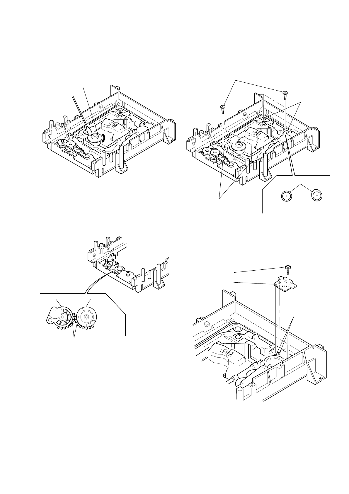
6-6. Note on Mounting TK-47 Board
1) Align two bosses. (See Fig. 13)
2) Align four tabs. (See Fig. 13)
3) Fix the board securely with 3 screws (BV3 × 10). (The sensor
will not function normally if the board floats up.)
Three screws
TK-47 board
Two claws
(BV3 × 10)
Boss
Two claws
Boss
Fig. 13
6-7. Note on connecting OPT Harness
1) The optical pick-up could be destroyed unless the OPT harness is connected normally to the connector. (See Fig. 14)
OPT harness
Good NG
Connector
Fig. 14
– 10 –
Page 11
SECTION 1
GENERAL
DVP-S7700
This section is extracted from AEP, UK model
instruction manual (3-864-941-31).
1-1
Page 12
1-2
Page 13
1-3
Page 14
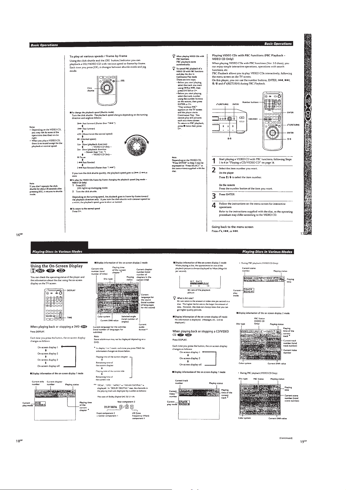
1-4
Page 15
1-5
Page 16
1-6
Page 17
1-7
Page 18
1-8
Page 19
1-9
Page 20
1-10
Page 21
1-11 E
1-11
Page 22
SECTION 2
DISASSEMBLY
Note: Follow the disassembly procedure in the numerical order given.
2-1. UPPER CASE REMOVAL 2-3. DOOR OPEN/CLOSE MOTOR
REMOVAL
DVP-S7700
1 Two tapping
screws
4 Upper case
3 Door open/close motor
CN-112 board
2 Four tapping
screws
1 Flat cable
(CN451)
2 Two screws
(PS3 × 4)
3 Two tapping
screws
2-2. FRONT PANEL REMOVAL
3 Three screws
(B3)
2 Connector
4 claw
5 Claw
(CN002)
7 Front panel
1 Font cable
(CN601)
6 Claw
2-4. MB-84 BOARD REMOVAL
7 Cover (upper)
5 Two screws
(B3)
1 Two connectors
(CN001, 002)
8 MB-84
board
2 Two flat cables
(CN301, 601)
6 Three screws
(B3)
3 Flat cable
(CN251)
4 Connector
(CN361)
9 Four flat cables
(CN101, 252, 302, 452)
2-1
Page 23
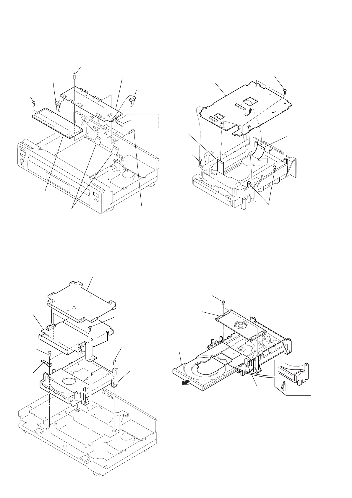
2-5. AU-218 BOARD REMOVAL
7 Two screws
3 Connector
(CN205)
1 Two screws
(B3)
(B3)
8 AU-218 board
4 Connector
(CN204)
2-7. TK-47 BOARD REMOVAL
4 Four screws
(BVTP3 × 10)
6 TK-47 board
2 Copper leaf plate
9 Two flat cables
(CN201, 203)
AEP, UK
5 Flat cable
(CN202)
6 Four screws
(BV/RING)
2 Flat cable
(spindle
motor)
(CN002)
1 Connector
(CN004)
2-6. MD BLOCK ASS’Y REMOVAL 2-8. TRAY REMOVAL
1 Cover (lower)
3 OP-15
flexible
board
(CN001)
5 Two claws
3 Chassis
bracket (B)
5 Two screws
(B3)
6 Clamp
2 Two screws
(B3)
4 Two screws
(B3)
7 MD block
ass’y
1 Two screws
(BVTP3 × 10)
2 Press pully bracket
4 Pull the tray.
6 Remove the
tray.
A
5 Claw
3 Rotate the cam gear
in direction A.
2-2
Page 24
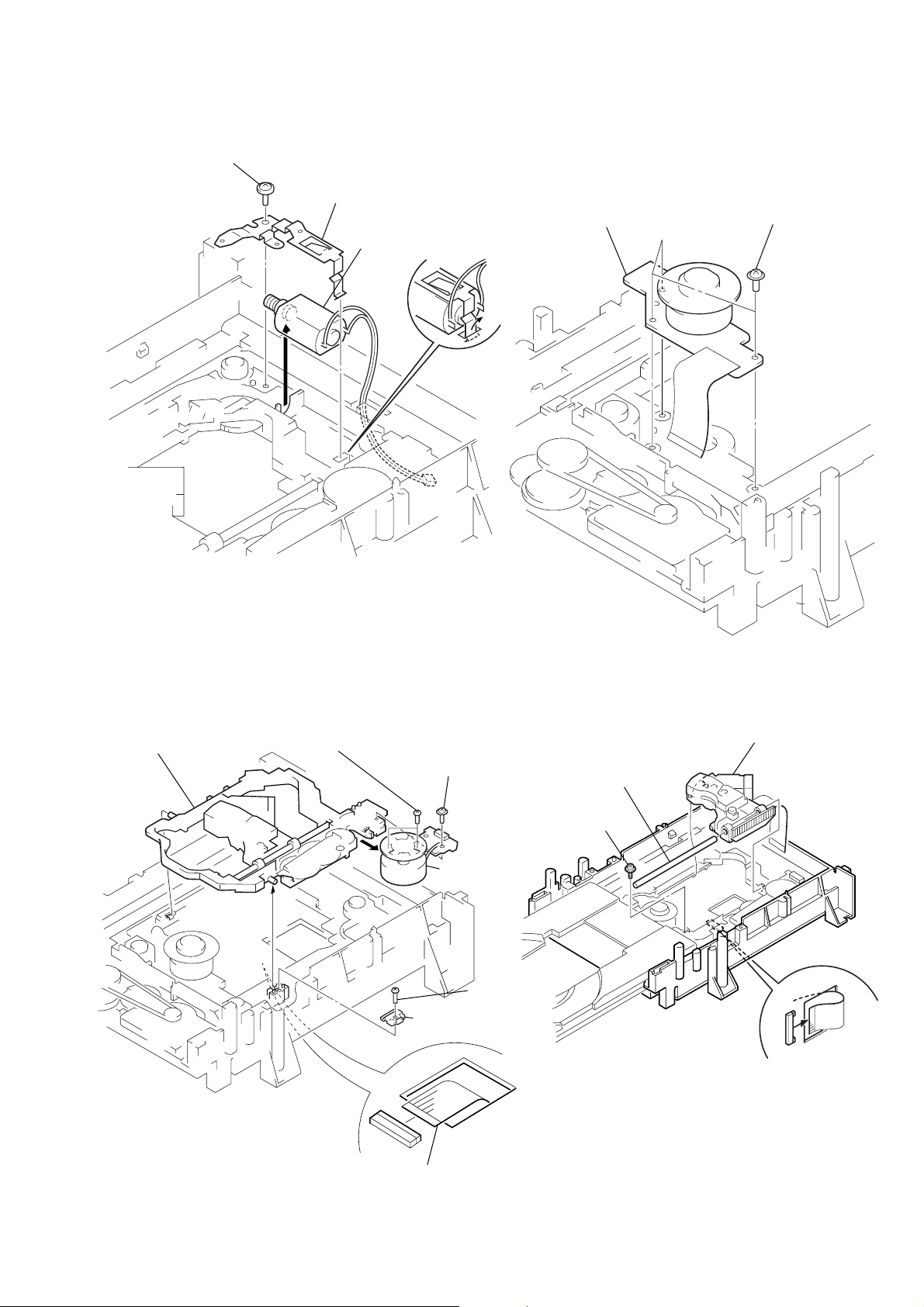
2-9. SKEW MOTOR (M903) REMOVAL
1 Three screws
(PTTWH2 × 5)
2 Spindle motor
(M901)
1 Screw
(PT WH2 × 5)
3 Skew gear retainer
4 Skew motor
(M903)
2-11. SPINDLE MOTOR (M901) REMOVAL
2 Claw
2-10. SLED MOTOR (M501) REMOVAL 2-12. OPTICAL PICK-UP REMOVAL
4 Spindle base
6 Two screws
(P1.7 × 2.5)
5 Screw
(PTTWH2 × 5)
3 Skew shaft
4 Optical pick-up
3 Main shaft
2 Screw
(PTTWH2 × 5)
7 Sled motor
(M501)
2 Screw
(P2 × 8)
stopper
1 OP-15 flexible board
(CN001)
1 OP-15 flexible
board
(CN001)
2-3
Page 25
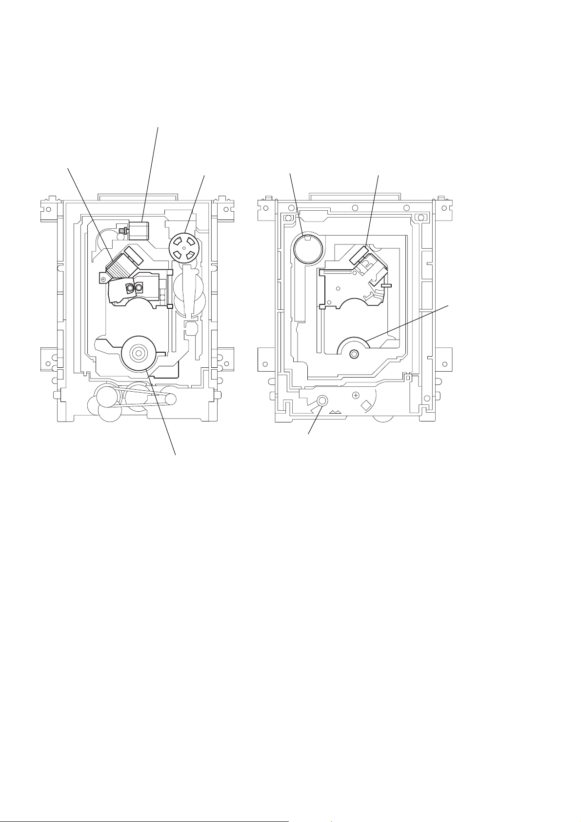
2-13. INTERNAL VIEWS
Skew motor ass’y (tilt)
X-3947-138-1
Optical pick-up
(KHS-180A/J1N)
8-820-005-02
Sled motor ass’y
X-3947-137-1
Sled motor ass’y
X-3947-137-1
Optical pick-up
(KHS-180A/J1N)
8-820-005-02
DC motor
(spindle)
1-698-944-11
DC motor (spindle)
1-698-944-11
Motor (loading)
1-698-942-21
2-4
Page 26
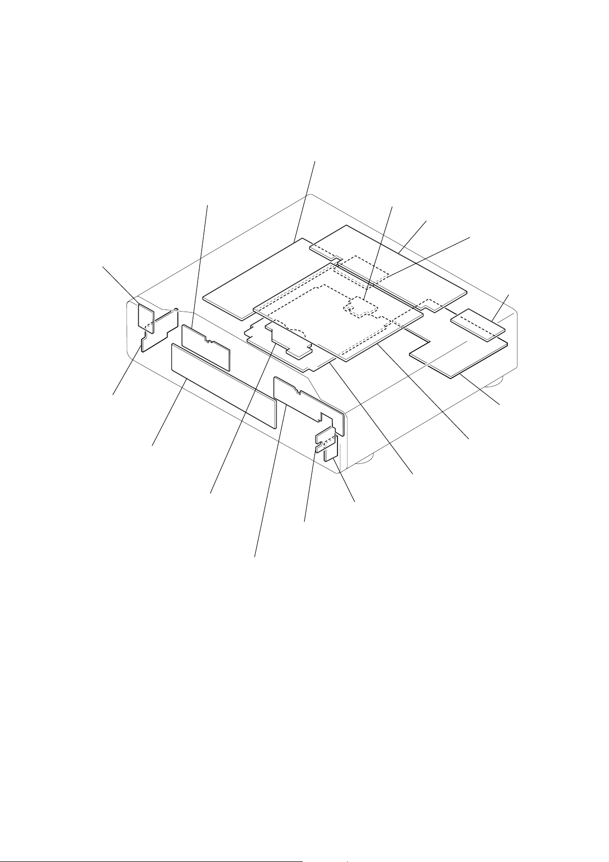
2-14. CIRCUIT BOARDS LOCATION
POWER BLOCK
(HS-930SH)
(SWITCHING REGULATOR)
FR-160
(FUNCTION SWITCH)
PW-120
(IR/POWER SWITCH)
HP-120
(HEAD PHONE)
FP-75
(FL DRIVER)
DC MOTOR
(SPINDLE)
DR-88
(DOOR SENSOR)
FL-108
(FUNCTION SWITCH)
FG-43
(SLED)
AU-218
(AUDIO)
TK-47
(RF/SERVO)
CN-113
(DOOR MOTOR)
PS-421
(AUDIO POWER)
YS-19
(COMPONENT
VIDEO)
ER-8 (AEP, UK)
(EURO AV)
MB-84
(SIGNAL PROCESS/
SERVO)
2-52-5 E
Page 27
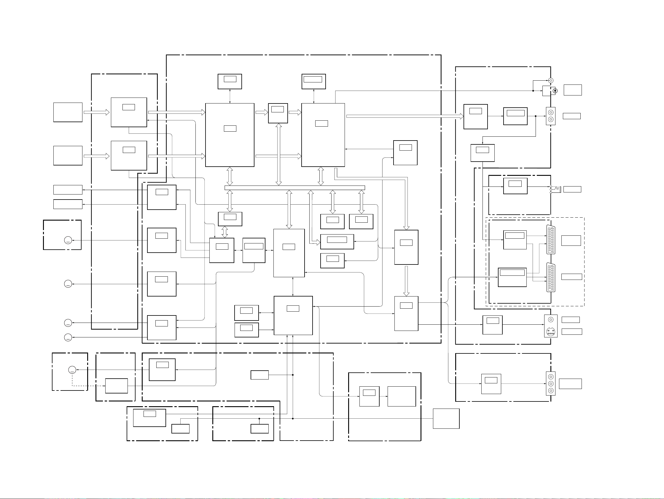
3-1. OVERALL BLOCK DIAGRAM
TK-47 BOARD
(SEE PAGE 4-11~4-14)
SECTION 3
BLOCK DIAGRAMS
MB-84 BOARD
(SEE PAGE 4-19~4-46)
IC810
16M DRAM
IC201, 202
16M SRAM
SPDIF
AU-218 BOARD
(SEE PAGE 4-51~4-56)
DIGITAL
OUT
DVP-S7700
DVD OPT
CD OPT
FOCUS COIL
TRACKING COIL
FG-43 BOARD
(SEE PAGE 4-30)
M503
M
SLED
MOTOR
M901
MOTOR
M902
MOTOR
M903
TILT
MOTOR
M
M
M
SPINDLE
LOADING
IC006
DVD RF AMP,
SERVO
IC005
CD RF AMP,
SERVO
IC363
FOCUS/TRACKING
COIL DRIVE
IC302
SLED MOTOR
DRIVE
IC303
SPINDLE MOTOR
DRIVE
IC361
TILT/LOADING
MOTOR DRIVE
DVD RF
CD RF
S GATE ARRAY
IC506
SERVO DSP
IC806
ARP
IC807
HA0-21, HD0-15
IC804 (1/2)
LGATE
ARRAY
IC603
ROM
IC605
RESET
SD0-7
CD_BCK,
CD_LRCK,
CD_DATA,
SPDIF
IC811
DECRYPT
SYSTEM µ-COM
DCRSD
IC851
IC604
IF µ-COM
0-7
IC203
AV DECODER
IC802
1M SRAM
IC804 (2/2)
L GATE ARRAY
IC801
EEPROM
AV_DATA, AV_BLK, AV_LRCK
YC0-7
IC803
8M ROM
IC207
OSD
IC251
DNR
IC252
VIDEO
ENCODER
Y0-7
C0-7
IC204
AUDIO 2CH
DAC
IC208
BUFFER
HP-120 BOARD
(SEE PAGE 4-70)
IC601-603, 607
SW, BUFFER
ER-8 BOARD
(SEE PAGE 4-63~4-68)
IC209
VIDEO
BUFFER
IC206, 207
FILTER AMP
BUFFER
IC001
HP AMP
IC604, 608
BUFFER
AUDIO
PHONE
AEP,UK
EURO AV1
(RGB)-TV
EURO AV2
VIDEO
S VIDEO
05
CN-113 BOARD
(SEE PAGE 4-77)
M451
M
DOOR
MOTOR
DR-88 BOARD
(SEE PAGE 4-77)
PH101, 102
DOOR
SWITCH
DOOR MOTOR
FL-108 BOARD
(SEE PAGE 4-77)
IC301
REMOTE CONTROL
RECEIVER
PW-120 BOARD
(SEE PAGE 4-78)
IC151
DRIVE
YS-19 BOARD
(SEE PAGE 4-57)
SWITCH
SWITCH
FR-160 BOARD
(SEE PAGE 4-78)
SWITCH
IC201
FL DRIVER
FP-75 BOARD
(SEE PAGE 4-73 )
ND201
FLUORESCENT
INDICATOR TUBE
TOUCH
SWITCH
BLOCK
3-1 3-2
IC851
VIDEO
DRIVER
COMPONENT
VIDEO
Page 28
DVP-S7700
3-2. RF/SERVO BLOCK DIAGRAM
OPTICAL DEVICE
SPINDLE
MOTOR
LOADING
MOTOR
CN-113 BOARD
(SEE PAGE 4-77)
M451
DOOR
MOTOR
CN451
M
IC006 ^£ – ^¢ (DVD play)
DVD PD IC
DVD LD
MODULE
SKEW
SENSOR
CD LASER
COUPLER
CD FOCUS
TRACKING
COIL
DVD FOCUS
TRACKING
COIL
M901
M
M902
M
D_MTR
1
3
800 mVp-p (V)
9
10
6
13
14
18
5
3
4
2
41
42
38
28
29
19
27
20
23
26
25
30
ı
33
34
ı
37
1
ı
8
9
ı
11
LDMT
DR-88 BOARD
(SEE PAGE 4-77)
CN101
1
3
RFP
RFN
A-D
VR
DVD LD
PD
VLD
SKEW IN
SKEW OUT
LED
PD1
PD2
AL
CD_E
CD_F
CD_LD
MON
VR
CD FCS,
CD TRK
DVD FCS,
DVD TRK
U IN,
V IN,
W IN,
SPVH
U OUT,
V OUT,
W OUT
PH101, 102
DOOR
SWITCH
TK-47 BOARD
(SEE PAGE 4-11~4-14)
CN001
9
10
6
13
14
18
5
3
SWITCH
4
2
SWITCH
41
42
38
28
29
19
27
20
23
SWITCH
26
25
30
ı
33
34
ı
37
CN002
1
ı
8
9
ı
11
CN004
1
2
CN102
D_MTR
4
5
D_SW1
2
D_SW2
1
Q004
Q005
Q001
LD ON
Q007
IC005 @™ (CD play)
500 mV/DIV 1 µs/DIV
FL-108 BOARD (1/2)
(SEE PAGE 4-77)
CN151
4
5
2
1
Q009, IC004
RF DET
IC006
DVD RF AMP, SERVO
63
RFP
HOLD1
64
RFN
10
A
ı
ı
7
D
1
A2
ı
ı
4
D2
SDATA
18
LD
17
PD
16
XLDON
FDCHG
20
TI-A
21
TI-B
3
PD1
4
PD2
5
E
6
F
1
LD
2
PD
APC_ON
IC005
CD RF AMP, SERVO
IC005 !£ (CD play)
500 mV/DIV 1 ms/DIV
IC151
DOOR MOTOR DRIVE
7
OUT1,2
9
SIGO
SCLK
ADEN
TIOFS
MIRR
MIRR
RF02
RF01
TE_C
IN1
IN2
RFO
MB-84 BOARD (1/6)
(SEE PAGE 4-27~4-34)
IC508
FILTER
2 1 6 7
CN005
CN008
CN501
26
9
23
10
11
3
19
18
17
4
20
22
27
16
21
13
14
15
12
2
1
16
ı
23
3
ı
10
11
ı
13
14
15
DVD_RF+
DFCTS
DVD_PI
TI-ERR
SCKG3
DVD_FE
DVD LDON
CDRFDC
CD LDON
TEATT
DVDFCS,
DVDTRK
CDFCS,
CDTRK
LDMT
TIMT
1
2
3
ı
8
TTLT/H
SSSD
SDEN
TIOFS
MIRR
CD TE
CD FE
57
47
37
PI
26
TIE
TII
23
TI–
24
43
44
45
19
33
TE
FE
30
19
21
22
13
TE
15
FE
32
25
12
VC
16
CN153
2
4
IC011
19
18
5
6
VC
DFWD
DRVS
DSW1
DSW2
SWITCH
SWITCH
338
139
13
12
FG-43 BOARD
(SEE PAGE 4-30)
Q008
10
9 11
IC005 !∞ (CD play)
500 mV/DIV 10 ms/DIV
VC
4
15
14
M903
TILT MOTOR
M501
SLED MOTOR
Q009
VC
M
M
IC501
IC502
HOLE SENSOR
TIE
DPD
CDRF
SVC
U IN,
V IN,
W IN,
SPVH
U OUT,
V OUT,
W OUT
SLDMT
HA, HB,
SLVH
2
19
18
17
25
9
10
11
24
8
6
1
12
7
15
14
13
16
26
27
12
5
25
18
17
15
13
14
1
2
7
8
1
6
19
18
5
ı
ı
ı
ı
5
6
CN452
CN302
CN361
CN301
CN601
IC502 (1/2)
3 1
TILT/LOADING
MOTOR DRIVE
8
DOUT2
9
5
DOUT1
6
DFWD
DRVS
DSW1
DSW2
DVD LDON
CD LDON
TILT/H
SSSD
SCKG3
SDEN
IC361
MUTE2
IN2–
IN1+
MUTE1
SYSTEM CONTROL
(SEE PAGE 3-9)
SYSTEM
CONTROL
(SEE PAGE 3-9)
VC
TRAY_FREE
13
OPN/CLS
17
21
S12VOFF
2
DVD RF
CD RF
TI_ERR
SIGNAL PROCESS
(SEE PAGE 3-5)
TIE
Q452
SWITCH
IC452
13
12
1
2
3
5
IC455
COMP
1
7
OUT
3
IN
5
TI_ERR
14
15
4
109 11
CD TRK
CDFCS
DVDFCS
DVDTRK
TIE
IN OUT
3 1
6 7
10 8
12 14
IC363
IC363
FOCUS/TRACKING
COIL DRIVER
11
DO2
12
13
DO1 MUTE2
14
15
DO4
16
17
DO3
18
SPINDLE MOTOR DRIVER
30
U IN
31
32
V IN
33
34
W IN
1
28
VH
29
23
U OUT
22
V OUT
19
W OUT
SLED MOTOR DRIVER
2
SLDMT
5
33
HA
34
29
HB
30
22
SLVH
23
MUTE1
IC303
Z1, Z2
SPCTRL1
SPCTRL0
SPGC2
SPGC1
IC302
IC503
IN2–
IN3–
IN1–
IN4–
HFG
NS+
DV–
DVI
DVO
TKC
CTRL
A+
IC501
COMP
IN2 OUT2
3 1
IN1 OUT1
IC502 (2/2)
5
10
12 14
Q371
9
MUTE
Q372
20
MUTE
6
23
3
26
14
15
27
7
8
9
10
11
8
12
13
18
25
32
PISW
7
8
IC301
19
20
–
671 2
+
CD/DVD
HFG
NST
SPCTRL1
SPCTRL0
SPGC2
SPGC1
TRAY_FREE
OPN/CLS
S12VOFF
89
TRIN
7
DFCTA
21
AIN5
AIN2
24
26
AIN0
GIO3
11
GIO2
12
8
GIO8
73
PWM2
99
TRREF
88
AIN6, 7
AIN8
18
2
GIO11
1
GIO12
49
AOUT0
AOUT1
46
IC506
SERVO DSP
HCK/HLDB
HDO-7
CLKIN
GIO10
MRST
GIO15
GIO13
HFD/HWR
HR/HRD
AOUT3
AOUT2
PWM1
PWM0
5
SYSTEM CONTROL
(SEE PAGE 3-9, 10)
TCK
IRS
GIO9
VTOP
VBTM
GIO0
MDS0
MDP0
72
56
ı
63
65
79
3
84
94
98
4
100
71
70
28
37
42
45
50
36
43
44
51
38
41
74
14
75
SIGNAL
PROCESS
(SEE PAGE 3-5)
HYCNTR
SDCNT
SOUT
SLOFS
TKC
HYCNTR
HYDET
SDCNT
SOUT
SLOFS
TKC
HYDET
IA1
IDO-7
27M_DSP
ACK
SYSTEM CONTROL
(SEE PAGE 3-9, 10)
SDPRST
ERROR
BUSY2
FON
SDSPWR
SDSPRD
IC507
POWER SUPPLY
7
OUT2
3
IN
5
OUT1
1
IC506 ^∞
3.6 Vp-p 27 MHz
IC303 !ª, @™, @£ (DVD play)
5.2 Vp-p 160Hz
IC303 !ª, @™, @£ (CD play)
1.84 Vp-p 45Hz
VC
05
3-3 3-4
Page 29
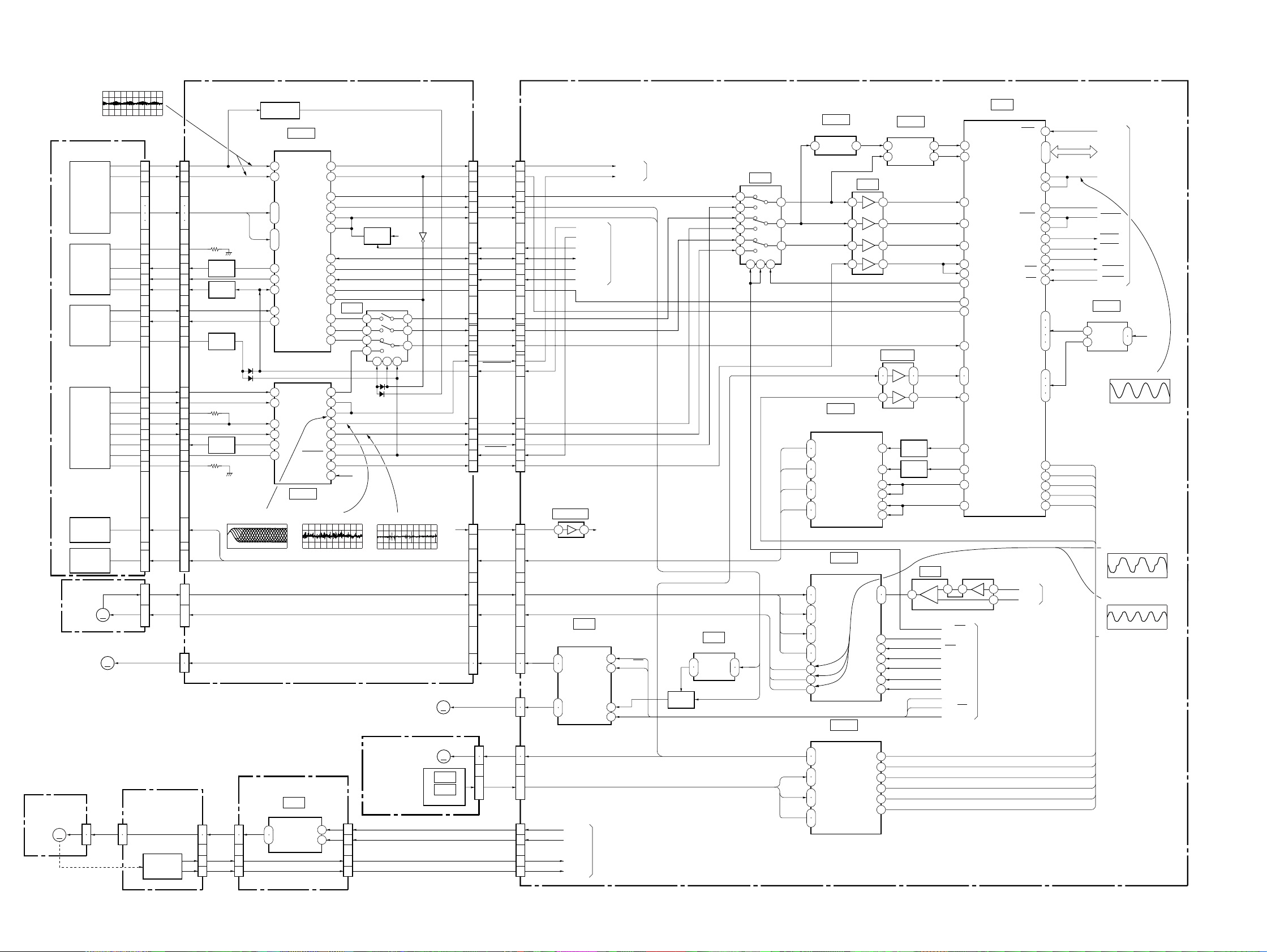
3-3. SIGNAL PROCESS BLOCK DIAGRAM
MB-84 BOARD (2/6)
(SEE PAGE 4-19, 4-41)
IC806 0
1.5 Vp-p
RF IN1DVD RF
10
RF IN2CD RF
RF/SERVO
(SEE PAGE 3-3, 4)
12
MDS0MDS0
43
MDP0MDP0
48
MA0-9
IC810
16M DRAM
MD00-15
IC806
ARP
XMWR, XCAS,
XRAS, XOE
SYSTEM CONTROL
(SEE PAGE 3-9, 10)
96
ı
99
SD0-7
101
ı
106
SDCK, XSHD,
106
XSRO, XSAK, SDEF
ı
109
IC207
OSD
SCLK
SO
SCLKO
CGCSO
OH SYNC
1
SD0-7 DCRSD0-7
3
74
77
DTI0-7
ı
79
80
4
ı
8
43-47 26-31 34-41
24
SIN
25
CS
26
EVEN
11
H SYVC
12
V SYNC
13
IC811
DECRYPT
XRST
54 51
SHA0-5
SHD0-7
R OUT
G OUT
B OUT
I OUT
DTO0-7
MCK
20
19
18
17
62
64
ı
66
68
ı
74
56
59
ı
61
AREQ, ALALID,
ERROR, TOS
VS
69
HS
70
88
ı
EX_OSD_0-3
91
12
ı
CH-DATA0-7
19
21
24
26
30
DCK
28
16M SDRAM
AVA0-11
AVID
IC201
0-15
SDQM, WE, CAS, RAS, CS1, CS2, SDQM, SDCLK
IC203
AV DECODER
IC202
16M SDRAM
PD0-7
DVP-S7700
73
74
76
ı
78
82
ı
84
FID
V SYNC
YC0-7
VIDEO
(SEE PAGE 3-7)
MUTE
MD2
DFCT
NORF
LOCK
FWON
ARPINT
ARPCS
ARPWT
SYSTEM CONTROL
(SEE PAGE 3-9, 10)
05
XWR
XRD
DCRCS
DCRINT
DCRWT
AVDRQ
AVCS
AVINT
AVWT
XRST
MRST
IA0-8
ID0-7
MUTE
110
MD2
112
DFCT
50
NORF
51
LOCK
53
FWON
55
XINT
80
XCS
81
83
XWAT
IC806 `⁄¤¤
3.4 Vp-p 27 MHz
XRST
84 122
XWR, XRD
XRST
MCKI
SCKI
124
33M
27M_DSP
70-73 75-7856 57
IA0-7
IC806 `⁄¤›
3.0 Vp-p 33 MHz
A0-7
56-62 64-67
ID0-7
D0-7
CD_LRCK, CD_BCK,
CD_DATA, SPDIF
106
ı
109
XRST
XWR, XRD,
DCRCS, DCRINT, DCRWT
IA0-5
ID0-7
27M_DNR
IC811 %¡
3.4 Vp-p 27 MHz
98
99
101
102
58 59 63-65 68 94-96 100 34-39 43-45 47-54
XWR, XRD,
AVDRQ, AVCS,
AVINT, AVWT
KESET_B
57
MRST
384FS
IA0-8
A_0-8
SPDIF_OUT
BCLK
LRCLK
ASDATA
D_0-7
ID0-7
111
105
106
107
SPDIF
AV_BCK
AV_LRCK
AV_DATA
384FS
27M_DNR
27M_DSP
33M
AUDIO
(SEE PAGE 3-11)
SYSTEM CONTROL
(SEE PAGE 3-10)
3-5 3-6
Page 30
DVP-S7700
3-4. VIDEO BLOCK DIAGRAM
MB-84 BOARD (3/6)
(SEE PAGE 4-23~4-26)
SIGNAL
PROCESS
(SEE PAGE 3-6)
SYSTEM
CONTROL
(SEE PAGE 3-9, 10)
MODE
CONTROL
(SEE PAGE 3-13)
05
YC0-7
FID
V SYNC
OHSYNC
27M_DNR
DCS
SCKG3
SOG3
AVCNT
E_V/RGB
YUV_RGB
AEP,UK
H SYNC
V SYNC
27M_VE
MRST
13.5M
VCS
AVCK
SOG2
VSI
VS
V SYNC
V MUTE
E_V/Y
EURO_V/Y
AV_CONT
E_V/RGR
YUY_RGB
OHSYNC
27M_DNR
DCS
SCKG3
SOG3
11
ı
GI 0-7
18
98 H SYNCI
9 BIO (27MHz)
29 XCS
30 XSCLK
31 SDI
IC251
DNR
XRST
DCLKI (13.5MHz)
93 100 97
MRST
13.5M
V SYNCI
G00-07
R00-07
AEP,UK:RGB output mode
IC252 &¢
0.7 Vp-p (H)
0.7 Vp-p (H)
IC252
VIDEO ENCODER
19
60
ı
67
51
ı
58
ı
22
PD0-7
24
ı
27
33
ı
36
PD8-15
38
ı
41
FID
14
V SYNC
15
16
H SYNC
PDCLK
XCS/SA
SCK/SCL
SI/SDASOVREF
XRST
SYSCLK
27M_VE
MRST
13.5M
4847 55454411108
VCS
AVCK
SOG2
VSI
IC252 %§
1.0 Vp-p
B-Y/R OUT
Y/G OUT
R-Y/B OUT
CPOUT
YOUT
COUT
RV251
VIDEO
LEVEL
ADJ
IC252 &™
74
72
66
56
64
58
IC252 ^¢
0.7 Vp-p (H)
IC252 ^§
0.7 Vp-p (H)
IC252 ^§IC252 &™IC252 &¢
0.7 Vp-p (H)1.0 Vp-p (H)
AV_CONT
Q638
VIDEO_B
EURO_V/Y
Hong Kong
VIDEO_R
VIDEO_G
6
Q601, 621, 624
AV CONT
Q639
BUFFER
Y
B-Y
R-Y
V MUTE
4
6
28
Q642
AV CONT L
AV CONT H
4
6
8
Hong Kong
V MUTE
2
EURO_V/Y
2
AV_CONT
3
E_V/RGB
9
YUV_RGB
1
AEP,UK
CN252 CN201
14
10
12
V MUTE
8
7
IC252 %•
0.7 Vp-p1.0 Vp-p
AEP,UK
E_V/RGB
YUV_RGB
178249
ER-8 BOARD (1/2)
(SEE PAGE 4-63~4-68)
CN603 CN604
B-Y
R-Y
V MUTE
VIDEO_V
VIDEO Y
VIDEO C
V MUTE
Q641
Y
VS
YS-19 BOARD
(SEE PAGE 4-57)
CN851CN251
4
6
8
2
12
16
14
18
19
14 15 5 3 1
VS
2 1 11 13 15
IC602
SWITCH
Q630
Q627
VIDEO C
V_MUTE
1
3
Q643,644
SWITCH
CONTROL
VIDEO Y
IC601
SWITCH
2
SWITCH
VIDEO V
CN602 (1/2)
AV CONT H
AV CONT L
Q632
IC851
VIDEO BUFFER
4 13
7
2
1
AU-218 BOARD (1/2)
(SEE PAGE 4-55)
Q218
BIFFER
CN202 (1/2)
3
1
2
7 4
7
4
AUDIO
(SEE PAGE 3-11)
Q215
INVERTER
5
IC851 !£
10
15
VIDEO BUFFER
2 15
4 13
7 10
1
VIDEO BUFFER
4 13
1
0.7 Vp-p (H)
IC209
VIDEO BUFFER
2 15
4
7
1
IC209 !£
1.0 Vp-p (H)
IC603
MUTE
IC607
107
MUTE
IC851 0
13
10
1.0 Vp-p (H)
Q214
VS
RY601
7
6
RY602
7
6
IC851 !∞
CB/B-Y
Y
CR/R-Y
IC209 0
8
5 1
RELAY DRIVE
58
RELAY DRIVE
0.7 Vp-p (H)
0.7 Vp-p (H)
Q628
1
Q629
J851
COMPONENT
VIDEO OUT
Y
C
Y
C
10
3
10
3
VIDEO 1
VIDEO 2
Hong Kong
S VIDEO 1
S VIDEO 2
Hong Kong
IC209 !∞
J202 (1/2)
LINE OUT
1.1 Vp-p (H)
Q602, 636
SWITCH
Q635, 637
SWITCH
20
19
15
11
7
16
8
20
19
15
11
7
16
8
V/Y IN
V/Y OUT
R/C
CNJ602 (1/2)
G
B
I
AV CONT OUT
V/Y IN
V/Y OUT
R/C
G
CNJ601 (1/2)
B
I
AV CONT IN
EURO AV1
(RGB)-TV
EURO AV2
3-7 3-8
Page 31

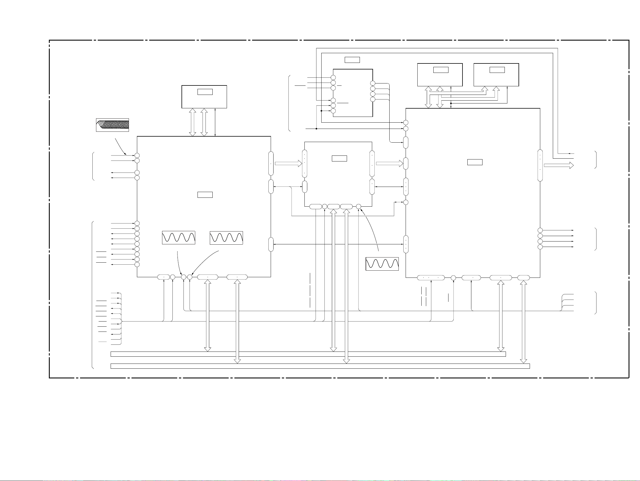
3-5. SYSTEM CONTROL BLOCK DIAGRAM
DVP-S7700
MB-84 BOARD (4/6)
(SEE PAGE 4-21, 4-39, 4-43,4-45)
AUDIO
(SEE PAGE 3-11)
RF/SERVO
(SEE PAGE 3-3, 4)
POWER
(SEE PAGE 3-16)
SIGNAL
PROCESS
(SEE PAGE 3-5)
MODE
CONTROL
(SEE PAGE 3-13)
SCKG3
SOG3
D2LT
DVDLDON
CDLDON
TILT/H
SSSD
SCKG3
SDEN
CD/DVD
NST
SPCTRL1
SPCTRL0
SPGC2
SPGC1
S12VOFF
TRAY_FREE
OPN/CLS
DFWD
DRVS
DSW1
DSW2
ERROR
BUSY2
FON
SDSPWR
SDSPRD
S12VOFF
MUTE
MD2
DFCT
NORF
LOCK
FWON
ARPINT
ARPCS
ARPWT
XRD
XWR
DCRCS
DCRINT
DCRWT
AVCS
AVWT
OHSYNC
XIFBSY
IFSI
IFSO
DIAG
XSHINT
IC801
EEPROM
SCKG3
SOG3
MLT
OHSYNC
EBSY, ECS,
EESI, EWC
46
47
117
50
2
3
13
52
48
4
7
8
9
10
22
19
18
5
112
142
111
12
15
14
17
77
58
104
103
105
106
16
102
60
59
61
56
57
62
63
64
65
66
140
132
44
109
125
133
SCKG3
SOG3
D2LT
MLT
DVDLDON
CDLDON
TILT/H
SSSD
SDEN
CD/DVD
NST
SPCTRL1
SPCTRL0
SPGC2
SPGC1
S12VOFF
TRAY_FREE
OPN/CLS
DFWD
DRVS
DSW1
DSW2
ERROR
BUSY2
FON
SDSPWR
SDSPRD
MUTE
MD2
DFCT
NORF
LOCK
FWON
ARPINT
ARPCS
ARPWT
IRD
IWR
DCRCS
DCRINT
DCRWT
AVCS
AVWT
OHSYNC
XIFBSY
IFSI
IFSO
DIAGN
XSHINT
IC804
L GATE ARRAY
HA0-7, 19-21
HD0-7
MRST
27M_VE
SCKG2
DOUTCTL
DCS
AVCNT
E_V/RGB
YUV_RGB
HSYNC
PDCLK
VCS
AVCK
VSI
IC807
1
ı
3
5
ı
8
ı
CGCS
SCLK
SI
SCKG1
SRST
HA0-8
HD0-7
CSI
SCKI
SDI
S GATE ARRAY
MODE
CONTROL
(SEE PAGE 3-13)
IC206 8
3.28 Vp-p 27 MHz
44
ı
50
IA0-8 IA1
52
53
33
ı
36
ID0-7
38
ı
41
57
SCO
56
SCKO
SDO
55
61
CK
384FS
33M
27M_DNR
27M_DSP
384FS_2CH
27M_DSP
IC204
716 2
SIGNAL
PROCESS
(SEE PAGE 3-6)
AUDIO
(SEE PAGE 3-11)
RF/SERVO
(SEE PAGE 3-4)
27M_DNR
27M_VE
ID0-7
IA0-8
ID0-7
CGCSO
SCLKO
SO
RF/SERVO
(SEE PAGE 3-4)
SIGNAL
PROCESS
(SEE PAGE 3-5)
VIDEO
(SEE PAGE 3-7)
IC802
1M SRAM
75
HA0-7, 19-21
76
83
ı
91
HD0-7
92
ı
99
HA0-21
23-30 32-39 41 42 44-47 4-11 13 14 16-21
RD, WR, CS0, CS1
RD, WR
73
74
XIRQ3, XIRQ7,
67
XCS6, XWAIT
68
71
72
SIG1, 2
69
70
108
123
115
113
158
49
150
149
151
148
127
118
36
114
37
152
VS
SOG1
48
49
57
59
2
55
56
69
107
109
108
54
MRST
SCK1
TXD1
PA11
112 110
65
PA0/CS4
53 64
A0-11
SYSTEM µ-COM
IC805 &£
PA10
IC804 `⁄⁄fi
3.3 Vp-p 27 MHz
IC805
4.4 Vp-p 20 MHz
A MUTE
MA MUTE
DOUTCTL
OHSYNC
SCKG3
SOG3
SOG3
DCS
E_V/YE_V/Y
AVCNT
E_V/
YUV_RGB
HSYNC
13.5M
VCS
AVCK
SOG2
VSI
VS
RGB
IC803
8M FLASH
HD0-15
AD0-15
AIDIO
(SEE PAGE 3-11)
AEP,UK
VIDEO
(SEE PAGE 3-7)
PB0
PB14/IRQ9
PA9
IRQ2
IRQ1
IRQ0
PB1
EXTAL
XTAL
SCK0
RES
HA0-8
HD0-7
97
1
63
68
67
66
98
73
74
111
79
MLT
SCKG3
SOG3
X201
27MHz
SYSCLK
(27MHz)
20MHz
CT201
ADJ
IC804 `⁄⁄°
X801
7
8
9
1
24
HFG
RF/SERVO
ACK
(SEE PAGE 3-4)
SDPRST
VIDEO
VSYNC
(SEE PAGE 3-7)
AVDRQ
SIGNAL
PROCESS
AVINT
(SEE PAGE 3-5)
XRST
SIGNAL PROCESS,
MRST
VIDEO, AUDIO
(SEE PAGE 3-5, 7, 11)
IC209
PLL
RSTB 384FS
ML
MC
MD
XT1
XT2
IC209 1
1.4 Vp-p 27 MHz
33M
27M
2010
21
63
64
11
14
16
19
23
24
25
IC205
BUFFER
5 6
2 3
12 11
IC206
BUFFER
24 3
5 6
12 11
9 8
225 mVp-p 13.5 MHz
05
3-9 3-10
Page 32

DVP-S7700
3-6. AUDIO BLOCK DIAGRAM
MODE CONTROL
(SEE PAGE 3-13)
SYSTEM CONTROL
(SEE PAGE 3-9)
SIGNAL PROCESS
(SEE PAGE 3-6)
SYSTEM CONTROL
(SEE PAGE 3-9,10)
MB-84 BOARD (5/6)
(SEE PAGE 4-21,4-23)
05
PMUTE
AUDIO MUTE
MA MUTE
AMUTE
SCKG3
D2LT
SOG3
SPDIF
AV_LRCK
AV_BCK
AV_DATA
DOUTCTL
384FS-2CH
MRST
CN252 (2/2)
IC208
CN101
20
AUDIO MUTE
17
19
18
16
5
4
5
3
1
8
MAMUTE
SCKG3
D2LT
SOG3
SPDIF OUT
DAC LRCK
DAC BCK
DAC DATA
384FS-2CH
MRST
AU-218 BOARD (2/2)
(SEE PAGE 4-51~4-56)
CN201 (2/2)
6
9
7
8
10
21
CN203
22
21
23
25
18
POWER
(SEE PAGE 3-15)
1
3
2
26
28
5
22
LRCIN
BCLK IN
D IN
ı
XTI
RSTB
PFAIL
FILTER SWITCH
IC204
AUDIO 2CH DAC
V_OUT L
ZEROR
V_OUT R
Q209
DRIVE
ZERO
HP_L
HP_R
COAXIAL
L
R
L
R
2
4
6
J201
OPTICAL
AUDIO1
AUDIO2
Hong Kong
PHONE
CN002
HP-120 BOARD
(SEE PAGE 4-70)
RV001
LEVEL
DIGITAL
OUT
J202 (2/2)
LINE
OUT
IC001
HP AMP
5 7
3 1
Q001, 002
MUTE
J001
PHONES
Q216
BUFFER
IC210
1
DIN
IC207
BUFFER
16
21
17
IC206
BUFFER
13
Q203
FILTER SWITCH
Q204
FILTER SWITCH
2 16 7
6 72 1
Q211
MUTE
Q210
MUTE DRIVE
Q217
MUTE DRIVE
Q212
MUTE
Q205
MUTE
IC208
HEAD PHONE AMP
3 1
5 7
CN205
5
3
PMUTE
1
AEP,UK
ER-8 BOARD (2/2)
(SEE PAGE 4-63,4-67)
VIDEO
(SEE PAGE 3-8)
AV CONT L
AV CONT H
CN202 (2/2)
CN602 (2/2)
MUTE_CTL
Q606, 640, 612
MUTE CTL
11 913
AU_R (X)
AU_L (X)
573
Q622, 623
MUTE
Q604, 605
MUTE
IC608
BUFFER
3 1
5 7
Q625, 626
MUTE
IC604
BUFFER
3 1
5 7
Q633, 634
MUTE
Q614, 615
MUTE
3
A (L) OUT
1
A (R) OUT
6
A (L) IN
2
A (R) IN
3
A (L) OUT
1
A (R) OUT
6
A (L) IN
CNJ602 (2/2)
EURO AV1
(RGB)-TV
CNJ601 (2/2)
EURO AV2
Q607, 608
MUTE
3-11 3-12
2
A (R) IN
Page 33

3-7. MODE CONTROL BLOCK DIAGRAM
MB-84 BOARD (6/6)
(SEE PAGE 4-37)
IC604
I/F µ-COM
VIDEO
SEE PAGE
3-7
POWER
SEE PAGE
3-16
AUDIO
SEE PAGE
3-11
SYSTEM
CONTROL
SEE PAGE
3-9, 10
VSYNC
VMUTE
P_CONT
IC605
RESET
PMUTE
AUDIO MUTE
XIFBSY
SCKGI
IFSI
IFSO
CGCS
SI
SCLK
DIAG
XSHINT
3OUT
SI
SCLK
53
REFV
27
VIDEO MUTE
33
P CONT
77
RESET IN
26
AUDIO MUTE
31 RESETSRST
16
INTMS
20
SCK
19
TX
18
RX
28
CGCS
32
PPG6
54 IFCS
SCLK
FLCS
AD6
AD4
AD3
X IN
X OUT
55
SO
22
24
30
25BZ
45
43
41
59IR
83
82
X601
4MHz
SI
SCLK
IC604 *™
5.6 Vp-p 4 MHz
ST-BY CONT 1 OUT1 IN1
A00–019 AD00–07
ALE, OE, WE
IC606
COMP
DVP-S7700
FP-75 BOARD
(SEE PAGE 4-73)
3
CN601
SI
10
SCKL
11
FLCS
12
BZ
13
AD6
17
AD4
16
IR
8
AD3
15
FL-108 BOARD (2/2)
(SEE PAGE 4-77)
CN153
10
11
12
13
17
16
8
15
Q151
BUFFER
DRIVE
RETURN
DVD
MENU
CN152
6
7
8
3
CN154
6
S155 S401
2
4
CN202
SI
6
SCLK
7
FLCS
8
D201
DTS
AD6
3
CN401
AD4
1
S404 S403 S402S159 S157
IR IR
5
AD3
3
FR-160 BOARD
(SEE PAGE 4-78)
IC 201
FL DRIVER
6
SI
8
SCLK
9
FLCS
dts
48
44
ı
G1–7 G1–7
38
15
ı
32
S1–19
•
35
49
PAUSE
50
PLAY
SEP UP
DNRPREVNEXTTITLE
CN402
4
2
ND201
FLUORESCENT
INDICATOR TUBE
5
ı
11
43
S1–19
ı
25
AD3
PAUSE_LED
PLAY_LED
PW-120 BOARD
(SEE PAGE 4-78)
CN301
2
EVER
5V
REG5V
4
CN201
2
6
AD6
3
IC301
REMOTE CONTROL
RECEIVER
1
Q301
LED
DRIVER
TOUCH
SWITCH
BLOCK
IC601
LATCH
05
IC603
ROM
S160
OPEN/
CLOSE
S158
PANEL
S156
ENTER
S154
RIGHT
S153UPS152 S151
DOWN
LEFT
S301
POWER
D303
ON/STANDBY
3-13 3-14
Page 34

DVP-S7700
3-8. POWER BLOCK DIAGRAM
AC IN
HS-930SH BOARD
(SEE PAGE 4-85)
CN101
F101
1
•
2
CN902
1
•
2
CN901
1
•
3
CN903
1
•
2
CN904
1
•
4
PS-421 BOARD
(SEE PAGE 4-81)
F901
D901, 902,
904, 905
D903
L101
LFT
RY901
CONT
Q951, 952
SWITCH
A+12V
AU–12V
P.FAIL
AU+12V
TK-47 BOARD
(SEE PAGE 4-11~4-14)
24
•
25
F004
F003
F002
F001
SYSTEM CONTROL
(SEE PAGE 3-9)
IC302
IC303
IC361
IC363
IC004 IC005
IC006 IC011
CN001
VCC
22
OPTICAL
DEVICE
D101
LF901
LFT
Q101–103
SWITCH
PC101
PHOTO
COUPLER
T101
CN202
3 1
Q311
5.2V REG
IC611
3.3V REG
Q211
12V REG
Q511
-12V REG
AEP,UK
P311
P312
P211
Q312
POWER
CONTROL
P511
Q512
-12V SWITCH
CN201 CN001
1
REG+5.2V
•
2
EVER+5.3V
6
REG+3.3V
4
P-CONT
8
AU+12V
9
M+12V
14
AU-12V
11
–12V
12
MB-84 BOARD
(SEE PAGE 4-19~4-46)
F006
7
F005
•
8
FL002
3
5
FL006
1
CN002
7
2
5
4
FL004
P_CONT
FL008
FL005
FL001
FL007
FL003
EVER+5.3V
MODE CONTROL
(SEE PAGE 3-13)
DP+5V
A+5V
AU+5V
S+5V
D+5V
EVER+5V
D+3.3V
IC301 IC452 IC455
IC501 IC502 IC503
IC506 IC507 IC508
CN302 CN008
3
•
4
IC802
IC801 IC803
IC804 IC805
IC807 IC811
Q001, 002
SWITCH
S12V OFF
IC812
LPF
S+5V
IC806
ER-8 BOARD (SEE PAGE 4-63~4-68)
IC202
+5V REG
Q213
+5V REG
CN601
1
IC604
IC608
3
CN602
CN202
IC204
IC206 IC207
IC208
IC602
IC601
IC607
IC603
CN604
9
8
A+5V
EVER 5V
78
E 12V
CN905
A+12V
1
Q202
+9V REG
Q201
–9V REG
P.FAIL
HP-120 BOARD
(SEE PAGE 4-70)
IC001
CN002
51
AU–9V
26
CN205
AUDIO
(SEE PAGE 3-11)
AU–12V
4
P.FAIL
5
AU+12V
7
CN204
Q206-208
1
SWITCH
4
5
7
AU-218 BOARD
05
(SEE PAGE 4-51~4-56)
E-12V
AU+9V
9
A+5V
IC209
IC210
Q205, 209
210, 211
YS-19 BOARD
(SEE PAGE 4-57)
IC851
CN851
1
CN201
11
17
22
5
1
HongKong
A+5V
EVER 5V
A+5V
D+5V
AU+12V
AU+5V
CN251
1
CN252
15
9
4
21
25
CN601
IC201 IC202 IC203
IC208 IC810
IC251
IC252
IC204 IC205 IC206
IC207 IC209
IC601 IC602 IC603
IC604 IC605 IC606
EVER+5V
1
D+5V
2
–10V
4
FL-108 BOARD
(SEE PAGE 4-77)
CN153
1
2
4
F151
DR-88 BOARD
(SEE PAGE 4-77)
PH101, 102
CN102
6
6
CN151
IC151
FR-160 BOARD
(SEE PAGE 4-78)
EVER 5V
D+5V
D+5V
–10V
CN401 CN402
1
5
FP-75 BOARD
(SEE PAGE 4-73)
CN202
2
4
IC201
Q202 ,203
DC-DC
CONVERTER
1
5
+F, -F
EVER 5V
D+5V
ND201
1
5
CN154 CN301
1
5
CN152
2
4
PW-120 BOARD
(SEE PAGE 4-78)
IC301
Q301
3-15 3-16 E
Page 35

SECTION 4
PRINTED WIRING BOARDS AND SCHEMATIC DIAGRAMS
DVP-S7700
THIS NOTE IS COMMON FOR PRINTED WIRING
BOARDS AND SCHEMATIC DIAGRAMS.
(In addition to this, the necessary mote is printed
in each block.)
For printed wiring boards:
• X : indicates a lead wire mounted on the component
side.
• x : indicates a lead wire mounted on the printed side.
• ® : Through hole.
• p : Parts mounted on the conductor side.
• b : Pattern from the side which enables seeing.
(The other layers’ patterns are not indicated.)
Caution:
Pattern face side: Parts on the pattern face side seen from
(Side B) the pattern face are indicated.
Parts face side: Parts on the parts face side seen from
(Side A) the parts face are indicated.
For schematic Diagram:
• Caution when replacing chip parts.
New parts must be attached after removal of chip.
Be careful not to heat the minus side of tantalum capacitor,
because it is damaged by the heat.
• All resistors are in ohms, 1/
unless otherwise specified.
kΩ : 1000Ω, MW : 1000kΩ.
• All capacitors are in µF unless otherwise noted. pF : µµF
50V or less are not indicated except for electrolytics and
tantalums.
• All variable and adjustable resistors have characteristic curve
B, unless otherwise noted.
• 2 : nonflammable resistor.
• 5 : fusible resistor.
• C : panel designation.
• ¢ : internal component.
• C : adjustment for repair.
• U : B+ Line.
• V : B– Line.
• Circled numbers refer to waveforms.
• Voltages are dc betw een measurement point.
• Readings are taken with a color-bar signals on DVD reference disc and when playing CD reference disc.
• Readings are taken with a digital multimeter (DC 10MW).
• Voltage variations may be noted due to normal production
tolerances.
Note: The components identified by mark ! or dotted line
with mark ! are critical for safety.
Replace only with part number specified.
4
W (Chip resistors : 1/
10
W)
When indicating parts by reference
number, please include the board
name.
4-1
Page 36

DVP-S7700
4-1. FRAME SCHEMATIC DIAGRAM (1/2)
FRAME (1/2)
4-3 4-4
Page 37

FRAME SCHEMATIC DIAGRAM (2/2)
DVP-S7700
4-5 4-6
FRAME (2/2)
Page 38

DVP-S7700
1-669-298-
05
(13)
13
TK-47
BOARD(SIDE A)
A
B
C
D
E
F
G
H
123456
48
33
32
17
16
1
64
49
48
25
32
1
8
9
16
17
24
4-2. PRINTED WIRING BOARDS AND SCHEMATIC DIAGRAMS
TK-47 (RF, SERVO) PRINTED WIRING BOARD
– Ref. No.: TK-47 board; 3,000 series –
TK-47 BOARD (SIDE A)
CN001 D-3
CN002 H-2
CN004 G-1
CN005 B-4
CN008 B-3
D003 C-4
D004 E-2
D006 F-5
IC004 C-4
IC005 D-4
IC006 F-3
IC011 E-5
Q001 E-2
Q004 E-2
Q005 E-2
Q007 D-4
Q008 F-3
Q009 F-3
Q010 D-3
There are few cases that the part isn't mounted in this model is printed on this diagram.
POWER BLOCK
(HS-930SH)
(SWITCHING REGULATOR)
PW-120
(IR/POWER SWITCH)
FR-160
(FUNCTION SWITCH)
FG-43
(SLED)
AU-218
(AUDIO)
PS-421
(AUDIO POWER)
YS-19
(COMPONENT
VIDEO)
HP-120
(HEAD PHONE)
FP-75
(FL DRIVER)
DC MOTOR
(SPINDLE)
DR-88
(DOOR SENSOR)
FL-108
(FUNCTION SWITCH)
TK-47
(RF/SERVO)
CN-113
(DOOR MOTOR)
ER-8 (AEP, UK)
(EURO A V)
MB-84
(SIGNAL PROCESS/
SERVO)
RF/SERVO
TK-47
4-7 4-8
Page 39

A
B
TK-47
BOARD(SIDE B)
DVP-S7700
DVP-S7700
C
D
E
F
G
H
05
123456
1-669-298-
13
(13)
RF/SERVO
4-9
TK-47
Page 40

DVP-S7700
• Waveforms
TK-47 (RF, SERVO 1) SCHEMATIC DIAGRAM
– Ref. No.: TK-47 board; 3,000 series –
1 IC006 %¡ – %™ (DVD play)
270 mVp-p (V)
2 IC006 ^¡ – ^™ (DVD play)
1.2 Vp-p (V)
3 IC006 ^£ – ^¢ (DVD play)
4 IC005 !£ (CD play)
500 mV/DIV 1 ms/DIV
5 IC005 !∞ (CD play)
500 mV/DIV 10 ms/DIV
6 IC005 @™ (CD play)
800 mVp-p (V)
500 mV/DIV 1 µs/DIV
Note:The components identified by mark ! or dotted line
with mark ! are critical for safety.
Replace only with part number specified.
DVD_FE
R018
22k
D006
MA151WA-TX
RF, SERVO 1
TK-47 (1/2)
4-11 4-12
Page 41

TK-47 (RF, SERVO 2) SCHEMATIC DIAGRAM
– Ref. No.: TK-47 board; 3,000 series –
DVP-S7700
4-13 4-14
RF, SERVO 2
TK-47 (2/2)
Page 42

DVP-S7700
IC803
1-671-899-
05
11
MB-84 BOARD(SIDE A)
A
B
C
1
2
3
4
5
6
7
8
D
E
F
1
7
18
R830
FG-43 BOARD
MB-84 BOARD (SIDE A)
CN001 F-1
CN002 E-1
CN251 A-8
CN303 A-5
CN361 B-8
CN451 A-3
CN601 E-8
CN801 F-5
D102 A-3
D801 F-6
IC203 D-2
IC205 C-6
IC206 D-6
IC251 B-2
IC252 A-2
IC301 A-6
IC303 A-6
IC455 C-3
IC501 A-5
IC506 C-4
IC508 B-5
IC603 F-6
IC604 E-7
IC803 F-4
IC804 E-6
IC805 E-3
IC806 B-4
Q371 C-3
Q372 C-4
Q501 A-5
MB-84 (SIGNAL PROCESS), FG-43 (SLED) PRINTED WIRING BOARDS
– Ref. No.: MB-84 board; 2,000 series, FG-43 board; 1,000 series –
There are few cases that the part isn't mounted in this model is printed on this diagram.
PW-120
(IR/POWER SWITCH)
HP-120
(HEAD PHONE)
FP-75
(FL DRIVER)
FR-160
(FUNCTION SWITCH)
DC MOTOR
(SPINDLE)
FL-108
(FUNCTION SWITCH)
POWER BLOCK
(HS-930SH)
(SWITCHING REGULATOR)
FG-43
(SLED)
CN-113
DR-88
(DOOR SENSOR)
(DOOR MOTOR)
AU-218
(AUDIO)
TK-47
(RF/SERVO)
PS-421
(AUDIO POWER)
YS-19
(COMPONENT
VIDEO)
ER-8 (AEP, UK)
(EURO A V)
MB-84
(SIGNAL PROCESS/
SERVO)
SIGNAL PROCESS, SLED
MB-84, FG-43
4-15 4-16
Page 43

1
24
25
40
41
64
65
80
1-671-899-
05
11
MB-84
BOARD(SIDE B)
A
B
C
1
2
3
4
5
6
7
8
D
E
F
1
7
18
R834
13
1
14
25
R911
1
2
2
1
DVP-S7700
MB-84 BOARD (SIDE B)
CN101 A-2
CN252 A-6
CN301 B-1
CN302 A-4
CN452 A-5
D002 E-8
D101 D-6
D103 D-6
D502 C-4
D503 C-4
D802 F-4
D803 F-2
IC201 C-7
IC202 D-8
IC204 B-6
IC207 B-7
IC208 C-7
IC209 D-2
IC302 B-2
IC361 C-2
IC363 C-5
IC452 A-4
IC502 B-4
IC503 B-4
IC507 C-4
IC601 F-2
IC602 F-3
IC605 E-2
IC606 F-1
IC801 E-3
IC802 F-4
IC807 F-6
IC810 B-5
IC811 D-7
IC812 B-6
Q001 E-7
Q002 E-7
Q452 C-5
4-17 4-18
SIGNAL PROCESS
MB-84
Page 44

DVP-S7700
MB-84 (AV DECODER) SCHEMATIC DIAGRAM • See page 4-15 to 4-18 for printed wiring board.
– Ref. No.: MB-84 board; 2,000 series –
AV DECODER
MB-84 (1/14)
4-19 4-20
Page 45

MB-84 (CLOCK GENERATOR) SCHEMATIC DIAGRAM • See page 4-15 to 4-18 for printed wiring board.
– Ref. No.: MB-84 board; 2,000 series –
DVP-S7700
• Waveforms
1 IC206 8
3.28 Vp-p 27 MHz
2 IC209 1
1.4 Vp-p 27 MHz
4-21 4-22
CLOCK GENERATOR
MB-84 (2/14)
Page 46

DVP-S7700
MB-84 (DNR) SCHEMATIC DIAGRAM • See page 4-15 to 4-18 for printed wiring board.
– Ref. No.: MB-84 board; 2,000 series –
DNR
MB-84 (3/14)
4-23 4-24
Page 47

DVP-S7700
MB-84 (VIDEO ENCODER) SCHEMATIC DIAGRAM • See page 4-15 to 4-18 for printed wiring board.
– Ref. No.: MB-84 board; 2,000 series –
• Wavef orms
1 IC252 &¢
0.7 Vp-p (H)
1 IC252 &¢
(AEP, UK model: RGB output mode)
0.7 Vp-p (H)
3 IC252 ^§
(AEP, UK model: RGB output mode)
0.7 Vp-p (H)
4 IC252 ^¢
1.0 Vp-p (H)
2 IC252 &™
1.0 Vp-p (H)
2 IC252 &™
(AEP, UK model: RGB output mode)
0.7 Vp-p (H)
3 IC252 ^§
5 IC252 %•
0.7 Vp-p (H)
6 IC252 %§
1.1 Vp-p (H)
0.7 Vp-p (H)
4-25 4-26
VIDEO ENCODER
MB-84 (4/14)
Page 48

DVP-S7700
• Wavef orms
1 IC303 !ª, @™, @£ (DVD play)
5.2 Vp-p 160 Hz
2 IC303 !ª, @™, @£ (CD play)
MB-84 (DRIVE 1) SCHEMATIC DIAGRAM • See page 4-15 to 4-18 for printed wiring board.
– Ref. No.: MB-84 board; 2,000 series –
1.84 Vp-p 45 Hz
DRIVE 1
MB-84 (5/14)
4-27 4-28
Page 49

MB-84 (DRIVE 2), FG-43 (SLED) SCHEMATIC DIAGRAMS • See page 4-15 to 4-18 for printed wiring boards.
– Ref. No.: MB-84 board; 2,000 series, FG-43 board; 1,000 series –
DVP-S7700
4-29 4-30
DRIVE 2, SLED
MB-84 (6/14), FG-43
Page 50

DVP-S7700
MB-84 (DSP 1) SCHEMATIC DIAGRAM • See page 4-15 to 4-18 for printed wiring board.
– Ref. No.: MB-84 board; 2,000 series –
DSP 1
MB-84 (7/14)
4-31 4-32
Page 51

MB-84 (DSP 2) SCHEMATIC DIAGRAM • See page 4-15 to 4-18 for printed wiring board.
– Ref. No.: MB-84 board; 2,000 series –
DVP-S7700
• Wavef orm
1 IC506 ^∞
3.6 Vp-p 27 MHz
4-33 4-34
DSP 2
MB-84 (8/14)
Page 52

DVP-S7700
MB-84 (BIAS) SCHEMATIC DIAGRAM • See page 4-15 to 4-18 for printed wiring board.
– Ref. No.: MB-84 boards; 2,000 series –
BIAS
MB-84 (9/14)
Note:The components identified by mark ! or dotted line
with mark ! are critical for safety.
Replace only with part number specified.
4-35 4-36
Page 53

MB-84 (IF µ-COM) SCHEMATIC DIAGRAM • See page 4-15 to 4-18 for printed wiring board.
– Ref. No.: MB-84 board; 2,000 series –
DVP-S7700
• Wavef orm
1 IC604 *™
5.6 Vp-p 4 MHz
4-37 4-38
IF µ-COM
MB-84 (10/14)
Page 54

DVP-S7700
• Wavef orms
MB-84 (L GATE ARRAY) SCHEMATIC DIAGRAM • See page 4-15 to 4-18 for printed wiring board.
– Ref. No.: MB-84 board; 2,000 series –
1 IC804 `⁄⁄°
225 mVp-p 13.5 MHz
2 IC804 `⁄⁄fi
3.3 Vp-p 27 MHz
3 IC806 0
4 IC806 `⁄¤›
3.0 Vp-p 33 MHz
5 IC806 `⁄¤¤
3.4 Vp-p 27 MHz
6 IC811 %¡
1.5 Vp-p
3.4 Vp-p 27 MHz
L GATE ARRAY
MB-84 (11/14)
4-39 4-40
Page 55

MB-84 (ARP, DECRYPT) SCHEMATIC DIAGRAM • See page 4-15 to 4-18 for printed wiring board.
– Ref. No.: MB-84 board; 2,000 series –
DVP-S7700
4-41 4-42
ARP, DECRYPT
MB-84 (12/14)
Page 56

DVP-S7700
MB-84 (SYSTEM µ-COM) SCHEMATIC DIAGRAM • See page 4-15 to 4-18 for printed wiring board.
– Ref. No.: MB-84 board; 2,000 series –
SYSTEM µ-COM
MB-84 (13/14)
4-43 4-44
Page 57

MB-84 (S GATE ARRAY) SCHEMATIC DIAGRAM • See page 4-15 to 4-18 for printed wiring board.
– Ref. No.: MB-84 board; 2,000 series –
DVP-S7700
• Waveform
1 IC805 &£
4.4 Vp-p 20 MHz
4-45 4-46
S GATE ARRAY
MB-84 (14/14)
Page 58

DVP-S7700
AU-218 (AUDIO) PRINTED WIRING BOARD
– Ref. No.: AU-218 board; 3,000 series –
AU-218 BOARD(SIDE A)
There are few cases that the part isn't mounted in this model is printed on this diagram.
11
05
POWER BLOCK
(HS-930SH)
(SWITCHING REGULATOR)
FR-160
(FUNCTION SWITCH)
PW-120
(IR/POWER SWITCH)
HP-120
(HEAD PHONE)
FP-75
(FL DRIVER)
DC MOTOR
(SPINDLE)
DR-88
(DOOR SENSOR)
FL-108
(FUNCTION SWITCH)
FG-43
AU-218
(SLED)
(AUDIO)
TK-47
CN-113
(DOOR MOTOR)
(RF/SERVO)
1-671-910-
PS-421
(AUDIO POWER)
YS-19
(COMPONENT
VIDEO)
ER-8 (AEP, UK)
(EURO A V)
MB-84
(SIGNAL PROCESS/
SERVO)
(11)
AUDIO
AU-218
4-47 4-48
Page 59

DVP-S7700
AU-218
BOARD(SIDE B)
COAXIAL
DIGITAL OUT
OPTICAL
S VIDEO OUT
VIDEO
LINE OUT
L
AUDIO
R
A
B
C
1-671-910-
05
1
2
3 4
AU-218 BOARD (SIDE B)
CN201 C-4
CN202 B-9
CN203 C-8
CN204 B-9
CN205 C-1
D201 C-8
D202 A-9
D203 A-9
D204 A-3
D205 A-3
D206 C-8
D207 A-3
D208 A-4
D209 C-8
D210 B-8
D211 B-8
D214 A-9
D216 A-7
IC202 B-8
IC204 C-6
IC205 A-8
IC206 B-7
IC207 B-4
IC208 B-1
IC209 B-2
IC210 A-2
Q201 B-8
Q202 A-9
Q203 B-5
Q204 B-6
Q205 B-8
Q206 A-10
Q207 A-10
Q208 A-10
Q209 B-7
Q210 B-7
Q211 B-5
Q212 B-6
Q213 A-7
Q214 B-3
Q215 B-3
Q216 A-1
Q217 B-7
Q218 C-4
5 6 7 8 9
11
(11)
4-49 4-50
AUDIO
AU-218
Page 60

DVP-S7700
AU-218 (AUDIO 1) SCHEMATIC DIAGRAM • See page 4-47 to 4-50 for printed wiring board.
– Ref. No.: AU-218 board; 3,000 series –
AUDIO 1
AU-218(1/3)
4-51 4-52
Page 61

AU-218 (AUDIO 2) SCHEMATIC DIAGRAM • See page 4-47 to 4-50 for printed wiring board.
– Ref. No.: AU-218 board; 3,000 series –
DVP-S7700
4-53 4-54
AUDIO 2
AU-218 (2/3)
Page 62

DVP-S7700
AU-218 (VIDEO BUFFER) SCHEMATIC DIAGRAM • See page 4-47 to 4-50 for printed wiring board.
– Ref. No.: AU-218 board; 3,000 series –
• Wavef orms
1 IC209 !∞
1.1 Vp-p (H)
2 IC209 !£
3 IC209 0
1.0 Vp-p (H)
0.7 Vp-p (H)
VIDEO BUFFER
AU-218 (3/3)
4-55 4-56
Page 63

DVP-S7700
YS-19 (COMPONENT VIDEO) PRINTED WIRING BOARD AND SCHEMATIC DIAGRAM
– Ref. No.: YS-19 board; 1,000 series –
YS-19
05
BOARD(SIDE A)
1-671-915-
There are few cases that the part isn't mounted in this model is printed on this diagram.
(11)
YS-19
11
05
BOARD(SIDE B)
POWER BLOCK
(HS-930SH)
(SWITCHING REGULATOR)
FR-160
COMPONENT VIDEO OUT
Y
B
/B-Y
C
CR/R-Y
1-671-915-
PW-120
(IR/POWER SWITCH)
HP-120
(HEAD PHONE)
11
(11)
(FUNCTION SWITCH)
FP-75
(FL DRIVER)
DC MOTOR
(SPINDLE)
DR-88
(DOOR SENSOR)
FL-108
(FUNCTION SWITCH)
FG-43
AU-218
(SLED)
(AUDIO)
TK-47
(RF/SERVO)
CN-113
(DOOR MOTOR)
PS-421
(AUDIO POWER)
YS-19
(COMPONENT
VIDEO)
ER-8 (AEP, UK)
(EURO A V)
MB-84
(SIGNAL PROCESS/
SERVO)
• Waveforms
1 IC851 !∞
2 IC851 !£
3 IC851 0
0.7 Vp-p (H)
0.7 Vp-p (H)
4-57 4-58
1.0 Vp-p (H)
COMPONENT VIDEO
YS-19
Page 64

DVP-S7700
ER-8 (EURO AV) PRINTED WIRING BOARD
– Ref. No.: ER-8 board; 1,000 series –
– AEP, UK –
There are few cases that the part isn't mounted in this model is printed on this diagram.
ER-8 BOARD (SIDE A)
D601 B-4
D607 A-5
D608 A-5
D609 A-6
D610 A-6
D616 A-2
D617 A-3
D618 A-3
D619 A-3
D620 A-4
D622 A-2
D623 A-2
D625 C-4
D626 C-2
D627 C-5
D628 B-2
D633 C-3
D634 C-3
IC603 B-2
IC604 B-4
IC607 B-3
IC608 B-5
Q601 C-4
Q602 C-6
Q604 B-4
Q605 B-4
Q607 A-4
Q608 B-4
Q612 C-5
Q614 A-5
Q615 B-5
Q622 B-5
Q623 B-5
Q625 A-5
Q626 B-5
Q633 A-6
Q634 B-6
Q635 C-5
Q636 A-4
Q637 C-5
Q638 C-4
Q639 C-4
Q643 C-3
Q644 C-3
A
B
C
ER-8
BOARD(SIDE A)
1-671-916-
11
(11)
FR-160
(FUNCTION SWITCH)
PW-120
(IR/POWER SWITCH)
HP-120
(HEAD PHONE)
FP-75
(FL DRIVER)
DC MOTOR
(SPINDLE)
POWER BLOCK
(HS-930SH)
(SWITCHING REGULATOR)
DR-88
(DOOR SENSOR)
FL-108
(FUNCTION SWITCH)
FG-43
AU-218
(SLED)
(AUDIO)
TK-47
CN-113
(DOOR MOTOR)
(RF/SERVO)
PS-421
(AUDIO POWER)
YS-19
(COMPONENT
VIDEO)
ER-8 (AEP, UK)
(EURO A V)
MB-84
(SIGNAL PROCESS/
SERVO)
D
05
1
2
3 4
5 6
EURO AV
ER-8
4-59 4-60
Page 65

ER-8
BOARD(SIDE B)
EURO AV2
DVP-S7700
EURO AV1
(RGB)-TV
A
B
C
1
2
2
9
21
20
1
1
2
21
20
ER-8 BOARD (SIDE B)
CN601 C-1
CN602 D-4
CN603 C-2
CN604 D-5
D602 A-3
D603 A-3
D604 A-2
D605 A-2
D606 A-1
D611 A-6
D612 A-6
D613 A-5
D614 A-5
D615 A-4
D621 A-2
D624 A-3
D631 B-5
D632 B-4
D635 D-5
D636 D-5
IC601 C-5
IC602 B-4
Q606 C-1
Q621 C-3
Q624 C-3
Q627 C-2
Q628 B-5
Q629 B-4
Q630 C-2
Q632 C-2
Q640 C-2
Q641 C-1
Q642 D-5
D
2
9
05
1
2
3 4
5
1
1-671-916-
6
11
(11)
4-61 4-62
EURO AV
ER-8
Page 66

DVP-S7700
ER-8 (EURO AV 1) SCHEMATIC DIAGRAM • See page 4-59 to 4-62 for printed wiring board.
– Ref. No.: ER-8 board; 1,000 series –
– AEP, UK –
EURO AV 1
ER-8 (1/3)
4-63 4-64
Page 67

ER-8 (EURO AV 2) SCHEMATIC DIAGRAM • See page 4-59 to 4-62 for printed wiring board.
– Ref. No.: ER-8 board; 1,000 series –
– AEP, UK –
DVP-S7700
4-65 4-66
EURO AV 2
ER-8 (2/3)
Page 68

DVP-S7700
ER-8 (EURO AV 3) SCHEMATIC DIAGRAM • See page 4-59 to 4-62 for printed wiring board.
– Ref. No.: ER-8 board; 1,000 series –
– AEP, UK –
EURO AV 3
ER-8 (3/3)
4-67 4-68
Page 69

HP-120 (HEAD PHONE) PRINTED WIRING BOARD AND SCHEMATIC DIAGRAM
1-671-918-
(12)
12
HP-120 BOARD(SIDE A)
05
– Ref. No.: HP-120 board; 1,000 series –
There are few cases that the part isn't mounted in this model is printed on this diagram.
DVP-S7700
HP-120
05
PHONES
BOARD(SIDE B)
PHONE
LEVEL
12
(12)
1-671-918-
FR-160
(FUNCTION SWITCH)
PW-120
(IR/POWER SWITCH)
HP-120
(HEAD PHONE)
FP-75
(FL DRIVER)
DC MOTOR
(SPINDLE)
POWER BLOCK
(HS-930SH)
(SWITCHING REGULATOR)
DR-88
(DOOR SENSOR)
FL-108
(FUNCTION SWITCH)
FG-43
AU-218
(SLED)
(AUDIO)
TK-47
(RF/SERVO)
CN-113
(DOOR MOTOR)
PS-421
(AUDIO POWER)
YS-19
(COMPONENT
VIDEO)
ER-8 (AEP, UK)
(EURO A V)
MB-84
(SIGNAL PROCESS/
SERVO)
HEAD PHONE
4-69 4-70
HP-120
Page 70

DVP-S7700
FP-75 (FL DRIVER) PRINTED WIRING BOARD
– Ref. No.: FP-75 board; 1,000 series –
There are few cases that the part isn't mounted in this model is printed on this diagram.
FP-75 BOARD (SIDEA)
CN201 A-10
D205 A-1
D206 A-1
Q202 A-1
FP-75 BOARD (SIDEB)
CN202 B-9
D201 B-3
D204 A-2
D209 B-1
IC201 A-5
Q203 B-1
FP-75 BOARD(SIDE A)
A
B
05
FP-75
1
BOARD(SIDE B)
A
1-671-913-
2
DTS
3 4
5 6 7 8 9 10
11
(11)
11
B
05
1
PW-120
(IR/POWER SWITCH)
HP-120
(HEAD PHONE)
FP-75
(FL DRIVER)
2
POWER BLOCK
(HS-930SH)
(SWITCHING REGULATOR)
FR-160
(FUNCTION SWITCH)
DC MOTOR
(SPINDLE)
FL-108
(FUNCTION SWITCH)
3 4
CN-113
DR-88
(DOOR SENSOR)
(DOOR MOTOR)
FG-43
(SLED)
AU-218
(AUDIO)
TK-47
(RF/SERVO)
5 6 7 8 9 10
PS-421
(AUDIO POWER)
YS-19
(COMPONENT
VIDEO)
ER-8 (AEP, UK)
(EURO A V)
MB-84
(SIGNAL PROCESS/
SERVO)
1-671-913-
(11)
FL DRIVER
FP-75
4-71 4-72
Page 71

FP-75 (FL DRIVER) SCHEMATIC DIAGRAM
– Ref. No.: FP-75 board; 1,000 series –
DVP-S7700
4-73 4-74
FL DRIVER
FP-75
Page 72

DVP-S7700
1-671-920-
05
(11)
11
DR-88
BOARD(SIDE A)
1-671-920-
05
(11)
11
DR-88
BOARD(SIDE B)
3
1
1
2
6
CN-113 (DOOR MOTOR), DR-88 (DOOR SENSOR), FL-108 (FUNCTION SWITCH), FR-160 (FUNCTION SWITCH), PW-120 (IR/POWER SWITCH) PRINTED WIRING BOARDS
– Ref. No.: CN-113 board, DR-88 board, FL-108 board, FR-160 board, PW-120 board; 1,000 series –
There are few cases that the part isn't mounted in this model is printed on this diagram.
FR-160 BOARD(SIDE A)
05
FR-160 BOARD(SIDE B)
SET UP
DNR PREV
NEXT
1-671-912-
11
(11)
FL-108 BOARD (SIDE A)
CN153 A-3
IC151 A-4
FL-108 BOARD (SIDE B)
CN151 A-4
CN152 A-1
CN154 B-1
Q151 B-5
FL-108
BOARD(SIDE A)
A
B
05
1
FL-108 BOARD(SIDE B)
1
2
TITLE
A
DVD
MENU
8
RETURN
1-671-911-
2
DOWN
LEFT
UP
3 4
RIGHT
62
1
ENTER
5
PANEL
OPEN/
CLOSE
11
(11)
05
PW-120
05
FUNCTION SWITCH, DOOR MOTOR
BOARD(SIDE A)
ON/
STANDBY
11
1-671-914-
CN-113, DR-88, FL-108, FR-160, PW-120
(11)
PW-120
05
BOARD(SIDE B)
1-671-912-
1
2
6
11
(11)
B
05
1
62
1
2
3 4
POWER BLOCK
(HS-930SH)
(SWITCHING REGULATOR)
FR-160
(FUNCTION SWITCH)
PW-120
(IR/POWER SWITCH)
FG-43
(SLED)
AU-218
(AUDIO)
PS-421
(AUDIO POWER)
YS-19
(COMPONENT
VIDEO)
POWER
1-671-914-
11
(11)
HP-120
(HEAD PHONE)
FP-75
(FL DRIVER)
DC MOTOR
(SPINDLE)
DR-88
TK-47
(RF/SERVO)
CN-113
(DOOR MOTOR)
ER-8 (AEP, UK)
(EURO A V)
MB-84
(SIGNAL PROCESS/
SERVO)
(DOOR SENSOR)
FL-108
(FUNCTION SWITCH)
4-75 4-76
CN-113
05
3
1
5
BOARD
1-671-919-
1-671-911-
11
(11)
11
(11)
Page 73

CN-113 (DOOR MOTOR), DR-88 (DOOR SENSOR), FL-108 (FUNCTION SWITCH), FR-160 (FUNCTION SWITCH), PW-120 (IR/POWER SWITCH) SCHEMATIC DIAGRAMS
– Ref. No.: CN-113 board, DR-88 board, FL-108 board, FR-160 board, PW-120 board; 1,000 series –
DVP-S7700
Note:The components identified by mark ! or dotted line
with mark ! are critical for safety.
Replace only with part number specified.
4-77 4-78
FUNCTION SWITCH, DOOR MOTOR
CN-113, DR-88, FL-108, FR-160, PW-120
Page 74

DVP-S7700
PS-421 (AUDIO POWER) PRINTED WIRING BOARD
– Ref. No.: PS-421 board; 1,000 series –
There are few cases that the part isn't mounted in this model is printed on this diagram.
PS-421 BOARD(SIDE A)
05
1-671-917-
11
(11)
PS-421
05
BOARD(SIDE B)
1-671-917-
11
(11)
FR-160
(FUNCTION SWITCH)
PW-120
(IR/POWER SWITCH)
HP-120
(HEAD PHONE)
FP-75
(FL DRIVER)
DC MOTOR
(SPINDLE)
POWER BLOCK
(HS-930SH)
(SWITCHING REGULATOR)
DR-88
(DOOR SENSOR)
FL-108
(FUNCTION SWITCH)
FG-43
AU-218
(SLED)
(AUDIO)
TK-47
CN-113
(DOOR MOTOR)
(RF/SERVO)
PS-421
(AUDIO POWER)
YS-19
(COMPONENT
VIDEO)
ER-8 (AEP, UK)
(EURO A V)
MB-84
(SIGNAL PROCESS/
SERVO)
AUDIO POWER
PS-421
4-79 4-80
Page 75

PS-421 (AUDIO POWER) SCHEMATIC DIAGRAM
– Ref. No.: PS-421 board; 1,000 series –
DVP-S7700
Note:The components identified by mark ! or dotted line
with mark ! are critical for safety.
Replace only with part number specified.
4-81 4-82
AUDIO POWER
PS-421
Page 76

DVP-S7700
POWER BLOCK (HS-930SH) (SWITCHING REGULATOR) PRINTED WIRING BOARD
– Ref. No.: HS-930SH board; 4,000 series –
There are few cases that the part isn't mounted in this model is printed on this diagram.
SWITCHING REGULATOR
POWER BLOCK (HS-930SH)
POWER BLOCK
(HS-930SH)
(SWITCHING REGULATOR)
FR-160
(FUNCTION SWITCH)
PW-120
(IR/POWER SWITCH)
HP-120
(HEAD PHONE)
FP-75
(FL DRIVER)
DC MOTOR
(SPINDLE)
FL-108
(FUNCTION SWITCH)
DR-88
(DOOR SENSOR)
4-83 4-84
FG-43
AU-218
(SLED)
(AUDIO)
TK-47
(RF/SERVO)
CN-113
(DOOR MOTOR)
PS-421
(AUDIO POWER)
YS-19
(COMPONENT
VIDEO)
ER-8 (AEP, UK)
(EURO A V)
MB-84
(SIGNAL PROCESS/
SERVO)
Page 77

POWER BLOCK (HS-930SH) (SWITCHING REGULATOR) SCHEMATIC DIAGRAM
– Ref. No.: HS-930SH board; 4,000 series –
12345678910
T101
A
HS-930SH BOARD
C112
0.047µF
630V
C113
470pF
2KV
D109
D1N60
436
337
Q103
2SK2563
SWITCH
R152
C114
+
1µF
400V
0.22
L150
45
!
D211
S2L20U
DVP-S7700
C213
47µF
B+
B+
B+
35V
B+
L211
10µH
2.6A
C211
+
330µF
35V
C212
47µF
+
35V
R211
11.8
10K
R212
11.8
Q211
2SJ488
REG
6.0
10K
!
P211
60V
750mA
C214
47µF
35V
++
B
C110
+
120µF
400V
C
D
2P
PS-421 BOARD
CN902
(SEE PAGE 4-81)
CN101
F101
1
250V
2
E
R104
470K
1/2W
2SK2563
SWITCH
R105
470K
1/2W
!
2A
Q101
!
C101
0.1µF
250V
337
R120
R106
R115
100K
100K
1/2W
1/2W
2.8
C117
0.0033µF
15K
R101
470K
1/2W
50V
D102
18V
1W
C102
!
0.1µF
L101
250V
18mH
0.5A
!!
C103
330pF
250V
Q102
2SC3377
SWITCH
D106
D1N60
C104
330pF
250V
L102
18mH
0.5A
2.8
0
C115
0.033µF
50V
!
C107
330pF
250V
D104
2.4V
R113
680
C116
0.01µF
50V
D101
S1NB60
!
C108
330pF
250V
R112
R116
220
2W
3.3K
R110
3.3K
R114
2.2K
D105
1SS270A
PC101B
TLP721F
PC101A
!
TLP721F
4.5
IC301
IC301
AN1431T
SHUNT REG
D311
D3S4M
D611
D3S4M
D511
S2L20U
R301
68
R303
1K
C301
+
1µF
50V
2.5
B+
C311
330µF
++
35V
D212
C511
1000µF
25V
B–
B+
L311
10µH
2.6A
C312
+
L511
10µH
2.6A
C611
560µF
35V
R304
1.5K
R305
330
R306
1.5K
C512
47µF
35V
330µF
35V
24V
1W
IC611
3.3V REG
IC611
PQ3RD13
4.2
I
O
G CT
3.1
+
C313
47µF
35V
+ +
3.3
Q312
2SC1740S
POWER
CONTROL
R314
10K
D312
0.2
1SS270A
R317
10K
R512
10K
–11.8
2SK2279
–12V REG
Q511
R311
1/2W
P312
60V
750mA
!
2SA1679
5.2V REG
–11.8
Q311
!
5.4
R514
P311
10K
60V
2.0A
5.3
4.7
Q512
2SA933S
–12 SWITCH
5.4
R312
1K
+
C411
R513
+ +
47µF
10K
35V
D313
2.7V
C315
10µF
+
C612
47µF
35V
C314
100µF
35V
50V
R511
10K
C513
+
47µF
35V
B–
!
P511
60V
750mA
B–
5.5
4.8
82
0.8
–3.2
B+
CN201 15P
1
REG +5.2V
2
REG +5.2V
3
GND (D)
4
REG +3.3V
5
GND (D)
6
EVER +5.3V
7
GND (D)
8
P-CONT
9
AU +12V
10
GND (AU)
11
AU –12V
12
REG
13
GND (D)
14
M +12V
15
GND (MTR)
B+
B–
CN202
B+
1
E+12V
2
GND
3
E–12V
B–
–10V
MB-84 BOARD (9/14)
CN001
(SEE PAGE 4-35)
MB-84 BOARD (9/14)
CN002
(SEE PAGE 4-35)
ER-8 BOARD(2/3)
CN601
(SEE PAGE 4-65)
05
F
NO MARK : E-E MODE
Note:The components identified by mark ! or dotted line
with mark ! are critical for safety.
Replace only with part number specified.
4-85 4-86 E
SWITCHING REGULATOR
POWER BLOCK (HS-930SH)
Page 78

SECTION 5
40, 41 AD2, 3 I Input of AD
42 GND – GND
43-46 AD4-7 I Input of AD
47 SDA – Not used
48 SCL – Not used
49-51 GND – GND
52 HSTX – Not used
53 REF V I Input of V SYNC
54 IFCS I Input of SH interrupt signal
55 ST-BY CONT I Input of ST-BY control signal
56 INT3 – Not used
57 CW – Not used
58 CCW – Not used
59 IR I Input of SIRCS
60 A1 IN – Not used
61 A1 OUT – Not used
62 DOT I – Not used
63 AC-3 OUT – Not used
64 STATUS – Not used
65-70 MODEL0-5 I/O Model select1-6
71 1C – Not used
72 1D – Not used
73, 74 MIC IN 1, 2 – Not used
75, 76 SW2, 3 – Not used
77 RESET IN I EXT RESET request
78-80 RCODE0 I/O REGION set1-3
81 GND – GND
82 X OUT O Output of X’tal(4MHz)
83 X IN I Input of X’tal(4MHz)
84 EVER 5V – Analog power supply
85-92 AD0-7 I/O Address and data set
93-100 A8-15 I/O Set address
5-1. INTERFACE CONTROL PIN FUNCTION (IC604 on MB-84 Board (10/14))
Pin No. Pin Name I/O Function
Pin No. Pin Name I/O Function
1-4 A16-19 I/O Set Address
5, 6 TIN0, 1 – Not used
7, 8 TOT0, 1 – Not used
9 ALE O Output of address latch inable signal
10 OE O Output of output inable signal
11 GND – GND
12 WRL O Output of write inable signal
13 WRH – Not used
14 HRQ – Not used
15 HAK – Not used
16 INTMS I Input of ready signal
17 CLK – Not used
18 RX I Input of serialbus0
19 TX O Output of serialbus0
20 SCK I/O Serialbus0
21 SI – Not used
22 SO O Output of serialbus1
23 EVER 5V – Digital power supply
24 SCLK I/O Serialbus1
25 BZ O Output of buzzer
26
AUDIO MUTE
O Output of audio mute signal
27
VIDEO MUTE
O Output of video mute signal
28 CGCS O Output of charactor generator chipselect
29 FL2CS – Not used
30 FLCS O Output of FLCS
31 RESET O RESET
32 PPG6 I Input DIAG
33 P.CONT O Output of POWER CONT signal
34, 35 EVER 5V – Analog power supply
36, 37 GND – GND
38 MIC CONT – Not used
39 ECHO CONT – Not used
IC PIN FUNCTION DESCRIPTION
DVP-S7700
5-1
Page 79

1 PB14/IRQ6 I Input of interrupt fromIC506
2 PB15/IRQ7 I Input of interrupt fromIC804
3 VSS – Digital ground
4-11 AD0-7 I/O Data bus AD0-7
12 VSS – Digital ground
13, 14 AD8, 9 I/O Data bus AD8,9
15 VCC – Digital power supply
16-21 AD10-15 I/O Data bus AD10-15
22 VSS – Digital ground
23-30 A0-7 O Addres bus A0-7
31 VSS – Digital ground
32-39 A8-15 O Addres bus A8-15
40 VSS – Digital ground
41, 42 A16, 17 O Addres bus A16,17
43 VCC – Digital power supply
44-47 A18-21 O Addres bus A18-21
48 CS0 O Chip select signal for external ROM(ICS803)
49 CS1 O Chip select signal for external ROM(IC802)
50 CS2 – Not used
51 CS3 – Not used
52 VSS – Digital ground
53 PA0/CS4 O Reset signal for IC101,209
54 PA1/CS5 O Output of reset signal
55 PA2/CS6 O Output of chip select signal to IC804
56 WAIT I Input of wait signal
57 WRL/WR O Output of write signal
58 WRH/LBS – Not used
59 RD O Output of read signal
60 PA7/BACK O Output of reset signal to IC508
61 VSS – Digital ground
62 PA8/BREQ O Output of reset signal to IC101
63 PA9 O Output of reset signal to IC506
64 PA10 O Output of A mute signal
65 PA11 O Output of MA mute signal
66 IRQ0 I Input of interrupt fromIC203
67 IRQ1 I Input of DMA request from IC203
68 IRQ2 I Input of V SYNC(FID) interrupt signal
69 IRQ3 I Input of interrupt from IC804
70 VCC – Digital power supply
71 CK O Output of internal clock
72 VSS – Digital ground
73 EXTAL – 20MHz crystal connection pin
74 XTAL – 20MHz crystal connection pin
75 VCC – Digital power supply
76 NMI I/O Hyper terminal pin
77 VCC (Vpp) – Digital power supply
78 WDTOVF – Not used
79 RES I Input of reset signal
80 MD0 I Input of mode select0 (fixed to 1)
81 MD1 I Input of mode select1 (fixed to 0)
82 MD2 I Input of mode select2 (fixed to 0)
83, 84 VCC – Digital power supply
85 AVCC – Analog power supply
86 AVREF – Reference power supply
87 PC0/AN0 I/O Set of mode 1
88 PC1/AN1 I/O Set of mode 2
89 PC2/AN2 I/O Set of mode 3
90 PC3/AN3 I/O Set of mode 4
91 AVSS – Analog ground
92 PC4/AN4 I/O Set of mode 5
93 PC5/AN5 I/O Set of mode 6
94 PC6/AN6 – Not used
95 PC7/AN7 – Not used
96 VSS – Digital ground
97 PB0 – HFG
98 PB1 O Output of reset signal for IC806
99 VCC – Digital power supply
100 PB2 – Not used
5-2. SYSTEM CONTROL PIN FUNCTION (IC805 on MB-84 Board (13/14))
Pin No. Pin Name I/O Function
Pin No. Pin Name I/O Function
5-2
Page 80

101 PB3 – Not used
102 PB4 – Not used
103 PB5 – Not used
104 PB6 – Not used
105 PB7 – Not used
106 VSS – Digital ground
107 RxD0 I Input of serial data
108 TxD0 O Output of serial data
109 RxD1 I Input of serial data
110 TxD1 O Output of serial data
111 SCK0 O Output of serial clock
112 SCK1 O Output of serial clock
Pin No. Pin Name I/O Function
5-3
5-3 E
Page 81

SECTION 6
TEST MODE
DVP-S7700
6-1. Starting up Test Mode
With the DVP-S7700 turned off, press [TITLE], [CLEAR], and
[POWER] keys on the Remocon in this order, and the Test mode
will start up and the Test Mode Menu as shown in Figure 1 will
appear on the video display.
Test Mode Menu
0. Syscon Diagnosis
1. Drive Auto Adjustment
2. Drive Manual Operation
3. Mecha Aging
4. Emergency History
5. Other Checks
Exit: POWER key
Figure 1
In the Test mode, use all keys on the Remocon or operation panel
when performing necessary operation. In any menu except during
test with the Syscon Diagnosis menu, press the [POWER] key to
exit from the Test mode, and return to the power off status.
Pressing [0] key on the Remocon during display of this initial menu
activates the Diagnosis mode and the screen as shown in Figure 2
appears.
Syscon Diagnosis
IF con Ver. →IFcon version (checksum)
SYScon Ver. →Syscon version (checksum)
(checksum of Syscon is
initially 0000)
Model No. DPX1178?? →Model code
** Press Remocon Key **
SIRCS:FF KEY:FF
Figure 2
6-2. Selection of Check Item
A check item can be selected when Model No. is displayed. Press
numeric keys to check the selected item, or any key other than
numeric keys to check all items.
Syscon Diagnosis
IF con Ver. 0.620 (9315)
SYScon Ver. 0.400 (0000)
Select Sub No. ; 02 - →Enter item No.[02]
** Press Remocon Key **
SIRCS:FF KEY:FF
Figure 4
Syscon Diagnosis
IF con Ver. 0.620 (9315)
SYScon Ver. 0.400 (0000)
Select Sub No. ; 02 - 0 →Enter item No.[02-0]
** Press Remocon Key **
SIRCS:FF KEY:FF
Figure 5
Syscon Diagnosis
IF con Ver. 0.620 (9315)
SYScon Ver. 0.400 (0000)
Press Enter ; 02 - 02 →Enter item No.[02-02]
** Press Remocon Key **
SIRCS:FF KEY:FF
Figure 6
Up to here, the [CLEAR] key can be used. Pressing [CLEAR] key
clears the selected number, and selection can be retried from the
beginning. If [ENTER] key is pressed, the diagnosis of only the
selected number is executed, and the result is displayed.
If any key is pressed while the result display is blinking, the screen
returns to the initial Test Mode Menu screen. Where visual check
is necessary such as a still picture check, or when an error occurred, use [PREV] key for repeated checking. To go to the next
step, press [NEXT] key.
If the diagnosis of selected number does not exist, the initial screen
is restored when [ENTER] key is pressed.
6-2-1. Selected Item Check
As the menu is not displayed, select the number from the list, and
enter 2-digit main item No. and 2-digit sub item No. using numeric keys on the Remocon. When the first one digit is entered,
the item selection screen is displayed. Then, enter remaining three
digits and press [ENTER] key.
When an item is selected, the detail check is executed where in
the case of RAM check, all addresses are checked twice by changing the data.
<Example> Select 2-2 ROM Check.
As item No. is <2-2>, enter “0202”.
Syscon Diagnosis
IF con Ver. 0.620 (9315)
SYScon Ver. 0.400 (0000)
Select Diag No. ; 0 - →Enter item No.[0]
** Press Remocon Key **
SIRCS:FF KEY:FF
Figure 3
6-2-2. All Items Check
Press any key other than numeric keys when Model No. is displayed to activate the all items check mode. In the all items check
mode, RAM check is simplified. In concrete, only the skipped
blocks such as 0-ff, 500-5ff, a00-aff, f00-fff, 1400-14ff, ... (addresses) are checked. Check is executed from the top item of the
diagnosis check items list sequentially. In a checking where visual
check is not necessary, check progresses to the next item automatically unless an error occurs.
In case of an error or visual check is necessary, press [PREV] ke y,
and the item concerned is repeatedly checked. To go to the next
item, press [NEXT] key.
6-1
Page 82

6-3. Error Display
(3) Destination Setting
In case of an error, the error code and information are displayed as
shown in Figure 7.
Syscon Diagnosis
IF con Ver. 0.620 (9315)
SYScon Ver. 0.400 (62ED)
RAM Check →Check item name
Error Code: 05 →Error code
Address : 01001D87 →Address where error occurred
Write Data: 20 →Written data (2 – 8 digits)
Read Data: FF →Read data (2 – 8 digits)
SIRCS:FF KEY:FF
Figure 7
When the Error Code is other than “05” (write/read data mismatch
error), the Address and Data become “0”.
“Diag OK” or “Diag Error End” message blinks, when the check
is all finished or stopped. Press a key here, and the screen returns
to the initial Test Mode Menu screen.
6-4. General Description of Checking Method
This section describes briefly a checking method of each diagnosis item, following the order of menu.
The number in ( ) in each item indicates a diagnosis item number.
(2) Memory
(2-2) Syscon ROM (IC803) Check
Checksum calculation
Error:Not detected
At addresses from 0x00000 to 0xfffff of Syscon ROM (IC803),
checksum is calculated by adding 8-bit data, and the result is displayed with 4-digit number in hexadecimal notation. As the error
is not detected, compare the displayed result with original ROM
checksum.
(2-3) Syscon RAM (IC802) Check (DMA used)
Syscon ROM (IC803) → Syscon RAM (IC802) matching check
Error 05: Write/read data mismatch error
External RAM (IC802) of IC805 (Syscon) is saved in the stack by
256 bytes each, and ROM data are transferred to the DMA. Then,
the data are compared with ROM (IC803) data ever y byte. In detail check, the bit inverted data are further written, and rec hecked.
During checking, all interruptions are stopped. Also, variables use
only the stacks including save area and bit inverted buffer. As a
processing is executed in the closed circuits within this function,
the data transfer to stack area also uses the DMA. In the detail
check, all areas of external RAM (IC802) are checked twice by
inverting the data, but in the simple check, one block is checked,
then the subsequent 4 blocks are skipped, and also a check of inverted data is not executed.
If write/read mismatch error occurred, checking can be repeated.
(3-2) Destination setting Check
I/O port read
Error:Not detected
The destination setting port (I/O) is read, and displayed with hex.
number.
Error is not detected.
(4) Gate Array (62000CFh: Peripheral Access Control)
(4-2) Register
Write data → Read data matching check
Error 05: Write/read data mismatch error
Register at adrs=62000CFh (Peripheral Access Control)
Whether written data and read data are matched is checked.
If write/read mismatch error occurred, checking can be repeated.
(4-3) Reset Line
Write → Hard reset → Read
Error 02: Reset error
0xff is written to the register (Peripheral Access Control) at
adrs=62000CFh, and whether it is initialized to “0x00” by the reset pulse is checked.
(5) Drive
(5-2) EEPROM (serial) (IC801)
Data write → Read matching check
Error 05: Write/read data mismatch error
11: Serial transfer error
12: EEPROM not ready
16-bit data is written to the address 0 of EEPROM (IC801), and it
is read to check for matching. Before checking, the content of address 0 is read for saving, but if it cannot be read, the error is
displayed and operation is terminated, and data writing is not executed.
In this diagnosis, 16-bit data is checked. 16 kinds of patterns are
written by shifting 1 bit each from 0x0001 toward the left.
If write/read mismatch error occurred, checking can be repeated.
Even if an error occurs after write/read check started, the saved
data are written when this diagnosis is quitted, but whether data
are written correctly is not guaranteed.
(5-3) SSI (Serial)
Serial register write → Register read matching check
Error 05: Write/read data mismatch error
33: SSI serial transfer error
0x00 – 0xff data are written to the FCCR register for SSI, then
they are read to check for matching.
If write/read mismatch error occurred, checking can be repeated.
6-2
Page 83

(5-5) Servo DSP Register
Data write → Read matching check
Error 04: Data read error
05: Write/read data mismatch error
13: DSP (IC506) data not ready
14: DSP (IC506) download error
The content of address 200h of DSP (IC506) is read for saving,
then checking starts. In this check, 16 kinds of patterns are written
to the address 200h by shifting 1 bit each from 0x0001 toward the
left, then they are read.
If write/read mismatch error occurred, checking can be repeated.
ROM (IC803) patterns are copied to all areas to be checked. Each
time 256 bytes are copied, the addresses of copy source (ROM)
are returned by 254 bytes. In detail check, all areas are checked to
verify all bits in DRAM (IC810), then the inverted data are further
checked in the same manner. The b us width of ARP (IC806) is 16
bits. This check program displays addresses in 16 bits.
Overwriting by the shadow can be detected, as the data are written
to all areas, then read. In the detail check, all areas of RAM (IC802)
are checked twice by inverting the data, while in the simple check
one block is checked, then subsequent 4 blocks are skipped, and
also inverted data are not checked.
If write/read mismatch error occurred, checking can be repeated.
(6-5) Interrupt Line in ARP (IC806)
(5-6) Servo DSP (IC506) Reset Line
Register write → Hard reset → Register read
Error 02: Reset error
13: DSP (IC506) data not ready
14: DSP (IC506) download error
The content of address 200h of DSP (IC506) is read, and after
hardware reset, the data is read again for comparison.
The check results in OK, if the register cannot be read, or data are
not matched even if it can be read. The reset error occurs if read
data are same as that before hardware reset.
In the case of ROM, whether the version No. is initialized by the
reset is checked. First, the version No. is read, then its complement is written.
After hardware reset, the data is read again and if it matches the
written data, the reset error occurs.
(6) Data Source
(6-2) Register in ARP (IC806)
Register write → Register read matching check
Error 05: Write/read data mismatch error
Data from “0x00” up to “0xff” are written to 12 registers where all
bits can be written and read, then read to check for matching.
If write/read mismatch error occurred, checking can be repeated.
(6-3) Reset Line in ARP (IC806)
Data transfer request → Data transfer stop interruption from ARP
(IC806)
Error 21: ARP (IC806) interruption is not detected
AC-3 audio data stored in ROM (IC803) are transferred to the
ARP (IC806), then the designated sector data output stop interruption from ARP (IC806) is detected.
To discriminate the Decrypt (IC811) interruption which is also
sent in the same line, the Decrypt (IC811) interruption is all masked.
(6-6) Register in Decrypt IC (IC811)
Register write → Register read matching check
Error 05: Write/read data mismatch error
0x00 – 0xfc data (lower 2 bits are masked) are written to the interrupt register, then read to check for matching.
If write/read mismatch error occurred, checking can be repeated.
(6-7) Reset of Decrypt IC (IC811)
Register write → Hard reset → Register read
Error 02: Reset error
05: Write/read data mismatch error
After “0xfc” is written to the interrupt register, whether it is initialized to “0x00” by the reset pulse signal is checked.
To make sure, the written data is read to check for matching before reset is executed.
Register write → Hard reset → Register read
Error 02: Reset error
05: Write/read data mismatch error
After “0xfe” is written to the INTEN3 register, whether it is initialized to “0x00” by the reset pulse signal is checked.
To make sure, the written data is read to check for matching before reset is executed.
(6-4) DRAM (IC810) in ARP
ROM data → ARP (IC806) → DRAM (IC810) → ARP (IC806)
read matching check
Error 03: Data write error (ARP (IC806) is not enabled for data
writing)
04: Data read error (ARP (IC806) is not enabled for data
reading)
05: Write/read data mismatch error
(6-8) Interrupt Line in Decrypt IC (IC811)
ROM (IC803) → ARP (IC806) → Decrypt (IC811)
Error 22: Decrypt (IC811) interruption is not detected
AC-3 audio data stored in ROM (IC803) are transferred to the
Decrypt via ARP (IC806), then the reserved data interruption fr om
Decrypt (IC811) is detected.
To discr iminate the ARP (IC806) interruption which is also sent in
the same line, the ARP (IC806) interruption is allmasked.
6-3
Page 84

(6-9) Reserved Data Head Byte Reading
(7-5) DRAM in AV Decoder (IC203)
ROM (IC803) → ARP (IC806) → Decrypt (IC811) reserved data
head byte read matching check
Error 05: Write/read data mismatch error
22: Decrypt (IC811) interruption is not detected
AC-3 audio data stored in ROM (IC803) are transferred to the
Decrypt via ARP (IC806), then the reserved data head bytes are
read from Decrypt (IC811) register.
As this audio data consists of 5 sectors, 0, 1, 2, 3, 4 data are written at the head of reserved data of respective sectors.
Whether these data are matched is checked through every sector
interruption.
If write/read mismatch error occurred, checking can be repeated.
(7) AV Decoder (IC203)
(7-2) Register in AV Decoder (IC203)
Register write → Register read matching check
Error 05: Write/read data mismatch error
“0x00” – “0xff” data are written to 51 registers where all bits can
be written/read, then they are read to check for matching.
If write/read mismatch error occurred, checking can be repeated.
ROM data → AV Decoder (IC203) → DRAM (IC810) → AV Decoder (IC203) read matching check
Error 03: Data write error
04: Data read error
05: Write/read data mismatch error
06: DMA transfer DREQ error
07: DMA transfer address error
ROM (IC803) patterns are copied to all areas to be checked. Because of large DRAM (IC810) capacity, each time 256 bytes are
copied, the addresses of copy source (ROM) are returned by 255
bytes. In detail check, to verify all bits in DRAM (IC810), the bit
patterns are checked again after inversion. DMA is used when
writing/reading the data. Though the bus width of AV Decoder
(IC203) is 64 bits, the display is given in 8 bits. Namely, actual
address is 1/8 of displayed data, and lower 3 bits indicate the byte
position.
Overwriting by the shadow can be detected, as the data are written
to all areas, then read. In the detail check, all areas of RAM are
checked twice by inverting the data, while in the simple c heck one
block is checked, then subsequent 4 blocks are skipped, and also
inverted data are not checked.
If write/read mismatch error occurred, checking can be repeated.
(7-6) Connection from ARP (IC806) to AV Decoder (IC203)
(7-3) Reset Line in AV Decoder (IC203)
Register write → Hard reset → Register read matching check
Error 02: Reset error
05: Write/read data mismatch error
After “0xff” is written to the Capture/Compare Control Register
0, whether it is initialized to “0x00” by the reset pulse signal is
checked.
To make sure, the written data is read to check for matching before reset is executed.
(7-4) DREQ Signal Line in AV Decoder (IC203)
AV Decoder (IC203) DMA check
Error 03: Data write error
04: Data read error
05: Write/read data mismatch error
06: DMA transfer DREQ error
07: DMA transfer address error
The connection of DREQ signal line to the AV Decoder (IC203)
is checked through DMA transfer.
If no error is found in DMA transfer, the transferred data are compared with the DRAM (IC810) data read from the register.
ROM data → ARP (IC806) → Decrypt (IC811) → AV Decoder
(IC203)
Error 04: Data read error
05: Write/read data mismatch error
06: DMA transfer DREQ error
07: DMA transfer address error
10: Chip-to-chip data transfer error
AC-3 audio data stored in ROM (IC803) are written to the ARP
(IC806), then whether they are transferred to the AV Decoder
(IC203) is checked. If transfer error is not detected, the address of
AV Decoder (IC203) to which data are transferred is displayed on
the terminal.
A part of data transferred to the AV Decoder (IC203) is read into
Syscon RAM (IC802) through DMA, and compared with ROM
(IC803) data.
(7-7) Interrupt Line in AV Decoder (IC203)
DRAM data of AV Decoder (IC203) → (DMA COPY) DRAM in
AV Decoder (IC203) another area
Error 31: AV Decoder (IC203) interruption is not detected
Data transfer stop interruption which is generated through
DMA copy of DRAM data in AV Decoder (IC203) to another area
is detected.
6-4
Page 85

(8) Video Consumption Concerned
(8-6) Still Picture Output (via ARP (IC806))
(8-2) Video Encoder (Serial) (IC252)
Color bar output (color bar enable command) from V ideo Encoder
(IC252)
Error 11: Serial transfer error
Using the Vsync interruption, serial communication to the Video
Encoder (IC252) starts, and the color bar enable command is transferred to the Video Encoder (IC252).
The Vsync interruption and internal serial 1 interruption are used.
If no error is found, the message is displayed to prompt for key
entry.
Check the color bar output.
(8-3) Video Encoder (IC252) Read
ID read → Existing data matching check
Error 40: Video Encoder (IC252) ID error
The Video Encoder (IC252) device ID is read.
Error if the read value is not “1914 (hex)”.
(8-4) Video Encoder (IC252) Vsync
CPU measures the Video Encoder (IC252) Vsync interrupt cycle.
ROM picture data → ARP (IC806) → AV Decoder (IC203) →
Video Out
Error 10: Chip-to-chip data transfer error
ROM (IC803) data are transferred to the AV Decoder (IC203) via
ARP (IC806), and the displayed picture is checked.
If no error is found, the message is displayed to prompt for key
entry.
The output picture is same as the start-up picture.
(8-7) DNR (Serial) (IC251)
ROM picture data → ARP (IC806) → AV Decoder (IC203) →
DNR (IC251) → Video Out (outline)
Error 10: Chip-to-chip data transfer error
Using special diagnostic command, the output still picture is transferred to the DNR (IC251) for checking.
If no error is found, the message is displayed to prompt for key
entry.
This checking is made only for the players with DNR (IC251).
The output picture used is same as that in (8-6) Still Picture Output.
The colors will vary extremely, if DNR (IC251) is effective.
For the players without DNR (IC251), the error code 0 is returned.
Error 41: Vsync interruption is not detected
42: Vsync interrupt cycle error
The number of interruption for 200 msec is counted, and if it is 11
to 13 times, this check is OK. It should be 12 times exactly , but ±1
errors are allowable.
(8-5) Still Picture Output (SDRAM (IC201, 202) direct write)
Pattern data → AV Decoder (IC203) → Video Out
Error 31: A V Decoder (IC203) interruption (DMA transfer) is not
detected
The pattern is directly written to the SDRAM (IC201, 202) of AV
Decoder (IC203), then its picture display is checked.
First, the brightness signal data are written by the amount of one
screen while changing every pixel.
For the color difference signals, both Cr and Cb are set to 80h for
monochromic pictures, and the display is turned on.
Then, color difference signal data are written while changing the
data every column.
As both brightness signal data and color difference signal data
take regular patterns, the processing speed is increased through
DMA transfer of the repeated sections.
Further, in detail check the color difference signal data written to
the out of display area are copied through DAM transfer to change
display colors successively.
If no error is found, the message is displayed to prompt for key
entry.
Check the pattern output.
(8-8) S Terminal DC Check
Color bar output by NTSC Encoder in Video Encoder (IC252)
Error 11: Serial transfer error
The color bars are output in the same manner as in (8-2).
After VS signal is turned on/off repeatedly two times, the color
bar output is turned off.
(8-9) EURO-AV Output Check (AEP, UK model)
Color bar output by video encoder (IC252)
ROM audio data → ARP (IC806) → AV Decoder (IC203) → 2ch
DAC (IC215) → Analog Audio Out
Error 11: Serial transfer error
10: ARP (IC806) n AV decoder (IC203) transfer error
35: 2ch DAC (IC215) serial transfer interruption is not de-
tected
37: PLL DAC (IC209) serial transfer interruption is not de-
tected
With AV-CONT : “H”, E-V/Y: “H”, E-V/RGB: “H”, video and audio signals are output.
For the video signals, the color bars are output same as in (8-2).
For the audio signals, MPEG audio signals of ROM (IC803) data
are output same as in (9-7).
6-5
Page 86

(8-10) Y/C Output Check (AEP, UK model)
(9-3) Sampling Frequency 48kHz
Color bar output by video encoder
Error 11: Serial transfer error
With AV-CONT: “H”, E-V/Y: “L”, E-V/RGB: “H”, video signals
areoutput.
For the video signals, the color bars are output same as in (8-2).
(8-11) RGB Output Check (AEP, UK model)
Color bar output by video encoder
Error 11: Serial transfer error
With AV-CONT: “H”, E-V/Y: “H”, E-V/RGB: “L”, video signals
areoutput.
For the video signals, the color bars are output same as in (8-2).
(8-12) AV CONT Wide Mode Check (AEP, UK model)
Color bar output by video encoder
Error 11: Serial transfer error
With AV-CONT: “H”, VS: “H”, video signals are output.
For the video signals, the color bars are output same as in (8-2).
18.4320MHz oscillation
Error 37: PLL DAC (IC209) serial transfer interruption is not de-
tected
Sampling frequency 48kHz is set to the PLL DAC (IC209).
If no error is found, the message is displayed to prompt for key
entry.
Observe the output waveform of IC209 (CXD8696R) SCK02 pin.
(9-4) Sampling Frequency 96kHz
36.8640MHz oscillation
Error 37: PLL DAC (IC209) serial transfer interruption is not de-
tected
Sampling frequency 96kHz is set to the PLL DAC (IC209).
If no error is found, the message is displayed to prompt for key
entry.
Observe the output waveform of IC209 (CXD8696R) SCK02 pin.
(9-5) Audio Digital Output
ROM audio data → ARP (IC806) → AV Decoder (IC203) → Digi-
tal audio I/F output
(8-13) AV CONT Through Check (AEP, UK model)
Color bar output by video encoder
Error 11: Serial transfer error
Input picture is sent as it is from EURO AV2 (CNJ601) to the AV1
(CNJ602).
The color bars are output from the player, same as in (8-2).
As AV-CONT output signal is turned on/off repeatedly tw o times,
confirm that the picture output is switched between through and
color bar alternately.
(8-14) Component Output Check
Color bar output by NTSC Encoder in Video Encoder (IC252)
Error 11: Serial transfer error
With AV-CONT : “H”, Component output “ON”, video signals are
output.
The color bars are output from the player, same as in (8-2).
(9) Audio Concerned
(9-2) Sampling Frequency 44.1kHz
16.9344MHz oscillation
Error 37: PLL DAC (IC209) serial transfer interruption is not de-
tected
Sampling frequency 44.1kHz is set to the PLL DAC (IC209).
If no error is found, the message is displayed to prompt for key
entry.
Observe the output waveform of IC209 (CXD8696R) SCK02 pin.
Error 10: ARP (IC806) → AV Decoder (IC203) data transfer er-
ror
37: PLL DAC (IC209) serial transfer interruption is not de-
tected
AC-3-audio bit stream data stored in R OM (IC803) are transferred
to the AV Decoder (IC203) via ARP (IC806), and output to the
digital audio interface.
If no error is found, the message is displayed to prompt for key
entry.
Analog outputs are muted.
(9-6) Audio Digital Mute
ROM audio data → ARP (IC806) → AV Decoder (IC203) → Digi-
tal Audio I/F output
Error 10: ARP (IC806) → AV Decoder (IC203) data transfer er-
ror
37: PLL DAC (IC209) serial transfer interruption is not de-
tected
AC-3-audio bit stream data stored in R OM (IC803) are transferred
to the AV Decoder (IC203) via ARP (IC806), and output to the
Digital Audio Interface. In such a case, the mute signal is turned
on/off alternately while the data are output 4 times.
1st time : Mute off Audible
2nd time: Mute on Not audible
3rd time : Mute off Audible
4th time : Mute on Not audible
If no error is found, the message is displayed to prompt for key
entry.
6-6
Page 87

(9-7) MPEG Audio Analog Output
g Error Codes in Diagnostic Test
ROM audio data → ARP (IC806) → AV Decoder (IC203) → 2ch
DAC (IC215) → Analog audio output
Error 10: ARP (IC806) → AV Decoder (IC203) data transfer er-
ror
35: 2ch DAC (IC215) serial transfer interruption is not de-
tected
37: PLL DAC (IC209) serial transfer interruption is not de-
tected
MPEG-audio bit stream data stored in ROM (IC803) are transferred to the AV Decoder (IC203) via ARP (IC806), and analog
audio data are output from 2ch DAC (IC215).
If no error is found, the message is displayed to prompt for key
entry.
(9-8) Dual DAC (Serial)
ROM audio data → ARP (IC806) → AV Decoder (IC203) → 2ch
DAC (IC215) → Analog audio output (Attenuation)
Error 10: ARP (IC806) → AV Decoder (IC203) data transfer er-
ror
35: 2ch DAC (IC215) serial transfer interruption is not de-
tected
37: PLL DAC (IC209) serial transfer interruption is not de-
tected
MPEG-audio bit stream data stored in ROM (IC803) are transferred to the AV Decoder (IC203) via ARP (IC806), and they are
attenuated by 12dB (-12dB) in the 2ch DA C (IC215), then analog
audio data are output.
If no error is found, the message is displayed to prompt for key
entry.
(9-9) Audio Mute Line
01: Mode not supported is selected
02: Reset error
03: Data write error
04: Data read error
05: Write/read data mismatch error
06: DMA transfer DREQ error
07: DMA transfer address error
10: Chip-to-chip data transfer error
11: Serial transfer error
12: EEPROM (IC801) is not ready
13: DSP (IC506) data is not ready
14: DSP (IC506) download error
21: ARP (IC806) interruption is not detected
22: Decrypt (IC811) interruption is not detected
31: AV Decoder (IC203) interruption is not detected
32: Servo DSP interruption is not detected
33: SSI interruption is not detected
34: DNR (IC251) interruption is not detected
35: 2ch DAC (IC215) interruption is not detected
36: EEPROM (IC801) interruption is not detected
37: PLL DAC (IC209) interruption is not detected
40: Video Encoder (IC252) ID error
41: Vsync interruption is not detected
42: Vsync interrupt cycle error
53: Video Encoder (IC252) interruption is not detected
90: Judged as error by inspector
91: Check of this item is quitted by key entry
92: Check of all items is quitted by key entry
93: Interruption by time over
99: Other errors
ROM audio data → ARP (IC806) → AV Decoder (IC203) → Analog audio output (Mute)
Error 10: ARP (IC806) → AV Decoder (IC203) data transfer er-
ror
35: 2ch DAC (IC215) serial transfer interruption is not de-
tected
37: PLL DAC (IC209) serial transfer interruption is not de-
tected
MPEG-audio bit stream data stored in ROM (IC803) are transferred to the AV Decoder (IC203) via ARP (IC806), and analog
audio data are output from 2ch DAC (IC215).
In such a case, first the mute by I/O of SH (IC805), then the mute
by setting AV Decoder (IC203), and by setting DAC are turned on
respectively to output low frequency tones.
Finally, the mute is turned off to output high frequency tones.
Checking is finished when high frequency tones are heard.
Low tones will be heard before this checking finished, if the mute
is not effective.
To make sure which mute is not effective, the check should be
repeated while paying attention to the message.
If no error is found, the message is displayed to prompt for key
entry.
6-7
Page 88

6-5. Drive Auto Adjustment
T-SKEW adjusting screw
The drive can be automatically adjusted, except disc change and
tangential skew adjustment. For a disc, use the disc for adjustment.
In case of abnormality, press the [STOP] key to stop adjustment.
If the drive does not stop, prev ent secondary failure by taking proper
action such as disconnection of the power cable. This adjustment
should be made after repair is finished and no trouble is present in
the drive.
A trouble, if present, causes NG and the adjustment to be aborted.
As the secondary failure could occur, perform automatic adjustment after the drive is completely repaired.
With the initial menu displayed, press [1] on standard commander ,
and the screen as shown in Figure 8 will appear.
Drive Auto Adjustment
SA.00000 SI.00 EMG.OO
Select No. ←Blinking
0: All 3: CD
2: DVD SL 4: DVD-DL
STOP: Press STOP Key
The tray opens after the [ENTER] key is pressed and the initialization is finished. Then, place the DVD_SL disc for adjustment.
Press the [ENTER] key to start adjustment. During adjustment,
the tangential skew adjustment screen is displayed. Make this adjustment only when the pickup was replaced.
As for adjustment, rotate the T-SKEW adjusting screw on the
pickup so that the displayed jitter becomes minimum (CCW makes
jitter smaller). Avoid extreme rotation or interference of screwdriver with the disc. After adjustment, a message to apply a screw
locking agent will be displayed if jitter value is within the specification. Then, apply a drip of locking agent to the recess of screw.
Hence, change discs following the given messages on OSD, and
the adjustment is finished if there is no problem.
Note that if “All” is selected, the data of previous adjustment are
erased and initial values are set.
Figure 8
If “All” is selected, the screen shown in Figure 9 is displayed.
Drive Auto Adjustment
SA.00000 SI.00 EMG.OO
0: Adjustment ALL
0: All 2: CD
2: DVD SL 3: DVD-DL
START: Press ENTER Key ←Blinking
STOP: Press STOP Key
Figure 9
Figure 10
6-8
Page 89

Drive Automatic Adjustment Flowchart
Loading
DVD_SL
adjustment
1
Adj. disc selection
Select “ALL”
EEPROM Default Set
Hydet Init
Sled Init
Go To Home Position
Select “ALL” or “SL”
DVD_SL
adjustment
Place DVD_SL
disc for adj.
Eject
YES
YES
NO
NO
FOK Check
OK
Tracking ON
Sled ON
AGC ON
CLVA
Lock Check
OK
Auto Loop Filter Offset
Auto Focus Offset
Auto Tilt Offset
Auto Focus Offset
servo stop
Go To Home Position
LD ON
Spindle start
Tilt ON
Focus ON
NG
NG
STOP
STOP
Loading
Disc T ype Check
OK
LD ON
Spindle start
Tilt ON
Focus ON
FOK Check
OK
sled move
Auto Tracking Offset
1
NG
NG
STOP
FOK Check
OK
Tan-Position
FOK Check
OK
Tracking ON
Sled ON
AGC ON
CLVA
Lock Check
OK
Tangential skew
adjustment
2
10k tj (rev)
NG
NG
NG
STOP
STOP
6-9
3
4
Page 90

DVD_SL
adjustment
CD
3
4 2
adjustment
5
6
Auto Loop Filter Offset
Auto Focus Offset
Auto Tilt Offset
Auto Focus Offset
Auto Focus Gain
Auto Tracking Gain
Auto EQ.
Auto Loop Filter Offset
Pull in Memory
Jitter Check
OK
Servo STOP
Search Check
OK
Eject
Lock screw
NG
NG
NG
STOP
FOK Check
OK
Auto Tracking Offset
FOK Check
OK
Tracking ON
Sled ON
CLVA
Lock Check
OK
Auto Loop Filter Offset
Auto Focus Offset
Auto Focus Gain
Auto Tracking Gain
Auto Loop Filter Offset
Pull in Memory
NG
NG
NG
STOP
STOP
STOP
CD
adjustment
Select “ALL” or “CD”
Disc change
DVD_SL n CD
Go To Home Position
Disc Type Check
Spindle start
YES
Eject
Loading
OK
LD ON
Tilt ON
Focus ON
NO
NG
Jitter Check
Servo STOP
Search Check
DVD_DL
adjustment
Select “ALL” or
Disc change
CD n DVD_DL
Go To Home Position
OK
OK
“DVD_DL”
YES
Eject
Loading
NG
STOP
NO
5
6
7
8 9
6-10
Page 91

DVD_DL
adjustment
7 10
8
adjustment
DVD_DL
9
Disc T ype Check
OK
LD ON
Spindle start
Tilt ON
Focus ON
FOK Check
OK
sled move
Auto Tracking Offset
FOK Check
OK
Tracking ON
Sled ON
AGC ON
CLVA
NG
NG
NG
STOP
STOP
FOK Check
OK
Tracking ON
Sled ON
CLVA
Lock Check
Layer Check
OK
Auto Focus Offset
Auto Tilt Offset
Auto Focus Offset
Auto Focus Gain
Auto Tracking Gain
Auto EQ.
Pull in Memory
Jitter Check
OK
NG
NG
NG
STOP
STOP
STOP
Lock Check
OK
Auto Focus Offset
Auto Tilt Offset
Auto Focus Offset
Auto Focus Gain
Auto Tracking Gain
Auto EQ.
Layer Check
OK
Jitter Check
OK
Focus Jump (L0 n L1)
10
NG
NG
NG
STOP
STOP
STOP
Servo Stop
Search Check
OK
Eject
Remove disc
Loading
End
NG
STOP
6-11
Page 92

6-6. Drive Manual Operation
6-6-3. Manual Control 1
In performing manual operation, observe the following points:
Select correct disc type on the Disc Type screen.
First, select “0. Disc Type” and execute “7. Hydet init” and “8.
Sled init”. (See Figure 12)
In case of abnormality, press [STOP] immediately to stop operation and turn off the power.
Do not execute Auto Adjust while executing FG Pause.
Also, as these commands are not protected, take care not to press
wrong key.
When PLL is locked, the sector address (or time code) is displayed
on the right side of SA.
6-6-1. Drive Manual Operation Menu Screen
Drive Manual Operation
SA.000000 SI.00 EMG.00
0. Disc Type
1. Manual Control 1
2. Manual Control 2
3. Manual Control 3
4. Manual Adjust 1
5. Manual Adjust 2
6. Auto Adjust
7. Check
Manual Control 1
SA.000000 SI.00 EMG.00
0. LD off 7. CLVA
1. SP off 8. CAV
2. Tilt off 9. Home
3. Focus off →. Sled FWD
4. Track off ←. Sled RVS
5. Sled off ↑ . Tilt Up
6. AGC off ↓ . Tilt Down
DVD SL 12cm
Figure 13
On this screen, turn on/off servo operation items necessary for
playing.
Normally, turn on the items from 0 sequentially, and normal trace
is executed at CLVA. In the tracking status, the sector address (or
time code (at CD)) is displayed.
If not displayed, the spindle is not locked, which means a failure.
In case of spindle system failure or no RF , the spindle system may
run, overriding the control.
In this case, do not press the CLVA.
Figure 11
This screen provides a menu for manual operation, and you can go
directly to each screen from here. To return to this screen from
each screen, press the RETURN key.
If [SET UP] button is pressed, the screen returns to the Test Mode
menu.
For switching between respective screens, use the [CLEAR] key.
6-6-2. Disc Type
Disk type
SA.000000 SI.00 EMG.00
0. DVD SL 12cm 9. Home
1. CD 12cm
2. DVD DL 12cm
3. DVD SL 8cm
4. CD 8cm
5. DVD DL 8cm
6. Disc type check
7. Hydet init
8. Sled init.
DVD SL 12cm
Figure 12
0. LD : Turn on/off the laser diode.
1. SP : Turn on/off the spindle.
At SP ON, the spindle runs in constant velocity mode.
2. TILT : Turn on/off the tilt servo.
3. Focus : Focus searching is executed and focus is turned on.
Operation is terminated if focus is not turned on after
focus search is retried about 3 times.
4. Track : Turn on/off the tracking servo.
5. Sled : Turn on/off the sled servo.
6. AGC : Turns on/off the focus error auto g ain control by PULL
IN level. (DVD only)
7. CLVA: Spindle normal servo.
8. CAV : Spindle in constant velocity mode
9. Home : Return to home position.
→. Sled FWD: Move the sled system outside.
Perform this with the tracking turned off.
←. Sled RVS : Move the sled system inside.
Perform this with the tracking turned off.
↑ . Tilt Up : Move the tilt system up.
↓ . Tilt Down : Move the tilt system down.
On this screen, select the type of disc used.
“6. Disc type check” judges the disc loaded. Confirm that judgment result meets the loaded disc type.
Judgment may fail if adjustment is not made yet immediately after EEPROM (IC801) Default Set. The CD which is not cut up to
the CD detection sensor position is judged as DVD. The optical
system will be damaged if other disc is loaded after selecting DVD
DL.
Be sure to set the disc type.
6-12
Page 93

6-6-4. Manual Control 2
Manual Control 2
SA.000000 SI.00 EMG.00
on.
9. LJ1→0 : After layer jump L1→L0, tracking loop turns
on.
→. FWD 1TJ : Jump one track forward.
←. RVS 1TJ : Jump one track reversely.
0. Pause off 4. Eject
1. FCS. Srch off 5. Load
6. Open
3. Tilt_H off 7. Close
DVD SL 12cm
Figure 14
Eject/Load are not used usually, because they can be done with
the [EJECT] button.
0. Pause : Pause is made by executing track jump once per
revolution.
1. FCS.Srch : The focus drive system is checked by applying
same voltage to the focus drive as that in focus
search.
3. Tilt H : Increase tilt gain.
4. Eject : Eject
5. Load : Loading
6. Open : Front door open
7. Close : Front door close
6-6-5. Manual Control 3
Manual Control 3
SA.000000 SI.00 EMG.00
0. FWD 32TJ 6. FT0→1
1. RVS 32TJ 7. FJ1→0
2. FWD 500TJ 8. LJ0→1
3. RVS 500TJ 9. LJ1→0
4. FWD 10KTJ →. FWD 1TJ
5. RVS 10KTJ ←. RVS 1TJ
DVD SL 12cm
Figure 15
On this screen, track jump, etc. are executed.
Confirm the sector information (SI) to check the DVD_DL layer
jump direction. Even SI means layer 0, or odd SI means layer 1.
When 1TJ or 32TJ is executed, the tracking is turned on, but the
sled becomes just like initialization.
Also, after executing each jump except 1TJ (and FJ1, 2), the CLV A
mode is set.
The optical system will be damaged if make a jump in
wrong direction FJ0, FJ1, LJ0 and LJ1.
6-6-6. Manual Adjust 1
Manual Adjust 1
SA.000000 SI.CD EMG.00
0. TRK. Off set xx
1. TRK. Off set 2 (DVD)
2. TRK. Gain 2 (CD)
3. Focus Gain
4. TRK. Gain
CD 12cm
Figure 16
On this screen, manual adjustment can be made where jitter measurement is not executed.
0. TRK. Offset
1. TRK. Offset 2 (DVD) : Adjust DVD tracking offset (TO TK-
2. TRK. Gain 2 (CD) : Adjust simple AGC of CD tracking.
3. Focus Gain : Adjust focus gain.
4. TRK. Gain
1
TRK. Offset : In the tracking offset adjustment for DVD, based
2
TRK. Gain :In the tracking gain adjustment for CD, based on
1
: Adjust tracking offset.
47 board, IC006). Adjusting range is
(A1 – AF) with
A1 – A7: +25 to +175 mV,
A8 – AF: 0 to –175mV.
Adjusting range is (88 – C8) with lower
4 bits fixed.
2
: Adjust tracking gain.
on the peak and bottom data measured by DSP
(IC506), the SSL33P3720A cansels the offset
roughly, then the DSP (IC506) adjusts it finely.
Here, finely adjusted value is set. As adjustment is
made by DSP (IC506) only.
DC component of tracking traverse does not change.
For the CD, only this set value changes.
the peak and bottom data measured by DSP (IC506),
the CXA2556 on the sets simple A GC to 5 ste ps of
–3.2, –1.6, 0, +1.6, +3.2 dB (Auto Tracking Offset), then the DSP (IC506) makes setting (Auto
Tracking Gain). Here, DSP (IC506) setting can be
made. In the case of DVD, only DSP (IC506) setting is executed.
0. FWD 32TJ : Jump 32 track forward (N track jump).
1. RVS 32TJ : Jump 32 track reversely (N track jump).
2. FWD 500TJ : Jump 500 tracks forward (fine search).
3. RVS 500TJ : Jump 500 tracks reversely (fine search).
4. FWD 10KTJ : Jump 10k tracks forward (direct search).
5. RVS 10KTJ : Jump 10k tracks reversely (direct search).
6. FJ0→1 : After layer jump L0→L1, tracking loop does not
turn on.
7. FJ1→0 : After layer jump L1→L0, tracking loop does not
turn on.
8. LJ0→1 : After layer jump L0→L1, tracking loop turns
6-13
Page 94

6-6-7. Manual Adjust 2
Manual Adjust 2
SA.000000 SI.00 EMG.00
0. Jitter on
1. Focus Offset xx
2. Tilt Offset
3. L.F. Offset
0204060
DVD_SL 12cm
Figure 17
On this screen, manual adjustment can be made where jitter measurement is executed.
0. Jitter : Turn on/off jitter measurement. Jitter will not
be measured unless the drive runs at CLV.
1. Focus Offset : Adjust focus offset.
2. Tilt Offset : Adjust tilt offset.
3. L.F. Offset : Adjust electrical offset in ARP (IC806).
3. Auto Focus Gain : Adjust focus gain automatically. Adjusted
result is reflected on the EEPROM (IC801).
Execute this with CLVA turned on if possible. If NG, the system will be defective,
and repair it.
4. Auto TRK gain : Adjust tracking gain automatically. Adjusted result is reflected on the EEPROM
(IC801). Execute this with CL VA turned on
if possible. If NG, the system will be defective, and repair it.
5. Auto EQ : Adjust RF equalizer properly. Adjusted result is not reflected on the EEPROM
(IC801). Execute this with CL VA turned on.
6. Auto L.F. Offset : Adjusts electrical offset in ARP (IC806).
The adjusted value is applied to the
EEPROM (IC801). During adjustment, lock
the CLV.
7. Memorize Pullin : Sets the pull-in level to the EEPROM
(IC801).
6-6-9. Check
check
SA.000000 SI.00 EMG.00
6-6-8. Auto Adjust
Auto Adjust
SA.000000 SI.00 EMG.00
0. Auto TRK. Offset xx xx
1. Auto Tilt Offset
2. Auto Focus Offset
3. Auto Focus Gain
4. Auto TRK. Gain
5. Auto EQ
6. Auto L.F. Offset
7. Memorize Pullin
DVD_SL 12cm
Figure 18
On this screen, each item can be automaticallyadjusted individually.
Note, however, that there are some restriction.
0. Auto TRK Offset : Adjust tracking offset automatically. Adjusted result is reflected on the EEPROM
(IC801). Turn off tracking with the Focus
turned on. Do not execute this at outside
track because pickup moves outside. In the
case of CD, tracking simple AGC is also
adjusted here.
1. Auto Tilt Offset : Adjust tilt offset automatically. Adjusted
result is reflected on the EEPROM (IC801).
Execute this with CLVA turned on. If NG,
retry this after focus offset and tangential
skew are adjusted.
2. Auto Focus Offset: Adjust focus offset automatically . Adjusted
result is reflected on the EEPROM (IC801).
Execute this with CLVA turned on. If NG,
retry this after tilt offset and tangential ske w
are adjusted.
1. EEPROM Default set (set)
6. EEPROM Data
DVD_SL 12cm
Figure 19
On this screen, various checking can be made. Note, howe ver , that
some items such as EEPROM (IC801) Default set are not reco verable.
1. EEPROM Default set : Use this to set EEPROM (IC801) set
values to default values. Before executing this, it is recommended to record
current values.
6. EEPROM data : Display EEPROM (IC801) set values
list.
Display is made with HEX numbers
“00” – “FF”.
6-14
Page 95

6-6-10. EEPROM Data Screen Display
EEPROM data
ID No. 00 SL L0 L1
Focus Offset 80 80 80 80
Focus Gain 30 18 30 30
TRK Offset 80 80 80 80
TRK. CONT. ?? ?? ?? ??
TRK Gain 30 30 30 30
Tilt Offset 80 80 80 80
Pullin Level 9e 9f ab ab
EQ. Boost ?? ?? ?? ??
L.F.O ?? ?? ?? ??
SD. ?? HY. ??
CD DVD
Figure 20
This screen displays various set values including adjusted results
stored in the EEPROM (IC801).
ID No. : Nothing is displayed (00 is displayed)
Focus Offset : 00 – FF 80 center (DVD_SL)
Focus Gain : 00 – 7F 20 center (DVD_SL)
TRK. Offset : 00 – FF 80 center (DVD_SL)
TRK. CONT. : Refer to Manual adjust 1 Tracking offset 2 and
Tracking gain.
TRK. Gain : 00 – 7F 20 center (DVD_SL)
Tilt Offset : 00 – FF 80 center (DVD_SL)
Pullin Level : 80 – FF D0 center (DVD_SL)
EQ. Boost : Fixed according to the disc type.
L.F.O : Only lower 5 bits are effective.
SD. : About 50 – E0
HY. : About 60 – A0
6-7. Other Operation
For manual operation of the drive, the following oper ations are
available, besides the operations given on the menu scr een. (Common to front panel and remote commander)
Eject/Loading
Clear CLEAR button
Stop STOP button Servo stop
Retrun RETURN button
Set up SET UP button STOP, then return to test
Cursol key →↑ keys
Cursol key ←↓ keys
Power POWER button Power OFF
OPEN/CLOSE
button
Stop+Ejection, and Loading
Movement throughout the
menu
Return to drive manual operation
mode menu
Increase manually adjusted
value
Decrease manually adjusted
value
6-15
Page 96

6-8. Emergency History
EMG Hist Page 4
With the initial menu displayed, press [4] key on the remote commander (RMT -D107E/D107P), and the information on emergenc y
history of Drvcon and Syscon will be displayed. This information
is given over four pages, which can be changed over with [↑] and
[↓] keys. To return to the initial menu, press [RETURN] key.
EMG Hist Page 1
CD 000000 Hour
1 00 00 00 00 00 00
00 00 00 00 00 00
2 00 00 00 00 00 00
00 00 00 00 00 00
Page Down: ↓ Exit: Return
N Page
N CD laser ON hours
N Emergency history
(latest)
N Emergency history (2)
Figure 21
EMG Hist Page 2
DVD 000000 Hour
3 00 00 00 00 00 00
00 00 00 00 00 00
4 00 00 00 00 00 00
00 00 00 00 00 00
Page UP : ↑
Page Down: ↓ Exit: Return
N DVD laser ON hours
N Emergency history (3)
N Emergency history (4)
DVD 000000 Hour
7 00 00 00 00 00 00
00 00 00 00 00 00
8 00 00 00 00 00 00
00 00 00 00 00 00
Page UP: ↑
Exit: Return
N Emergency history (7)
N Emergency history (8)
Figure 24
The following hidden commands are available. Data clear can be
confirmed from the fact that the screen display changes.
Clearing laser ON hours
Press [DISPLAY] and [CLEAR] keys on the remote commander
(RMT-D107E/D107P) in this order.
Clearing emergency history
Press [TITLE] and [CLEAR] keys on the remote commander
(RMT-D107E/D107P) in this order.
After repair is finished, always clear emergency history data.
Clearing Syscon preset
Press [DVD MENU] and [CLEAR] keys on the remote commander
(RMT-D107E/D107P) in this order.
For EMG code, Mech mode, and Disc information of history display, see “Emer gency code list”, “Mech mode list”, and “Disc type
list”.
Figure 22
EMG Hist Page 3
CD 000000 Hour
5 00 00 00 00 00 00
00 00 00 00 00 00
6 00 00 00 00 00 00
00 00 00 00 00 00
Page UP : ↑
Page Down : ↓ Exit: Return
Figure 23
N Emergency history (5)
N Emergency history (6)
6-16
Page 97

How to see Emergency History
1 2 3
Etc
90: Fail in servo recovery when starting up the disc.
91: Took more than 30 seconds when starting up the
disc.
92: The number of the times of servo error at re-
covery is over regulation.
96: Auto Sequence Time Out
97: Auto Sequence Fail
1 EMG CODE
2 MECHA MODE
3 DISC TYPE (Mecha Mode: 6π)
1 EMG CODE (Emergency code list)
Digital Pass
01: EEPROM (IC801) Write NG
02: EEPROM (IC801) Read NG
03: EEPROM (IC801) Busy Time Out
04: Emergency History Pointer NG
06: IFCON SYSCON Communication NG
07: IFCON V-sync NG
Electrical Adjustment
10: EEPROM (IC801) Check NG
16: DSP (IC506) Check NG
Mecha
20: Home Position Time Out
21: Sled Driver NG
22: Sled NG
26: Tray NG
28: Door NG
Tilt/Adaptation
30: Hy Det Level NG
31: Sled Offset Cancel NG
32: Focus Gain NG
33: Tracking Offset NG
34: Tracking Gain NG
35: Jitter NG
Focus
40: Focus Servo Lock NG
41: Focus Jump NG
Spindle
60: Miss Chuck
61: Spindle Lock Time Out
62: Spindle Reckless
63: CLV Lock NG
64: CLV Lock Time Out
65: CAV Speed NG
66: Spindle Speed × 1 NG
Seek System
70: Req Address NG
71: Req Time Code NG
72: Req Track No. NG
73: Seek NG
Data Relation
80: Address Continuity NG
81: Address Read NG
82: TOC Read Time Out
83 – 87: Physical Information Read Error
88: Layer No. NG
89: CD Text Data Read Error
Syscon
A0: Stop request from drive controller was received
A1: At the mode change command, the mode could
not be changed within specified time and the
drive stopped.
A2: Retry due to supply error failed and the drive
stopped.
A3: Disc directory configuration and information file
are illegal and the drive stopped.
A4: The drive stopped as a DVD-R disc was used.
A5: Coded data could not be decoded and the drive
stopped.
A6: At slow R, the destination of reverse search is
illegal and the drive stopped.
A7: Supply error and stopped.
B0: SYSCON error was due to supply system.
B1: SYSCON error was due to VIDEO hung up
B2: DMX error
B3: At slow R, data supply time out
B4: At slow R, wrong Navi Pack sector address
B5: At slow R, VIDEO hung up
B6: At slow R, Gttgt end time out
B7: At FF/FR, data supply time out
B8: At FF/FR, VIDEO hung up
IFcon
C0: IFCON ROM destination is wrong
C1: IFCON UART1 communication port NG
Power system
D0: The power turned off because of power off re-
quest from drive controller.
D1: The mode change to Stop mode failed and the
power turned off.
Drvcon
E0: DRVCON system error
E1: DRVCON system error
2 MECHA MODE (Mecha mode list)
00: Power ON Ready
10: Stop
20: Trace (data supply mode)
30: Pause
40: Drvcon Initialize
50: Mecha Initialize
6π: Spin Up
61: Adaptation (Tracking Offset)
62: Adaptation (Jitter/Gain)
63: TOC/Control Data Read
60: Etc
70: Spin Down
80: Seek
90: Error Recovery
6-17
Page 98

3 Disc Type (Mecha Mode: 6π)
6
6-9. Error Code
(A) (B)
The self-diagnosis function works to prevent the player from malfunctioning, a five-digit service number (combination of a letter
and figures) flashes on the screen and front panel display.
1. Each user needs to manage the error........................ “C” code
(A) Last result of disc type judgment.
(B) Initial result of disc type judgment.
Disc type list
FF: Unknown
00: No Disc
01: CD 12 cm
11: CD 8 cm
02: Single DVD 12 cm
12: Single DVD 8 cm
03: Dual DVD 12 cm
13: Dual DVD 8 cm
04: CDR 12 cm
14: CDR 8 cm
05: DVDR 12 cm
15: DVDR 8 cm
C : 13 : ππ • The disc is dirty.
→ Clean the disc with a cleaning cloth.
C : 31 : ππ • The disc is not inserted correctly.
→ Open the disc tray and insert the disc
correctly.
MECHA MODE is shown in ππ position.
Code Description
00 Power ON Ready
10 Stop
20 Trace (data supply mode)
30 Pause
40 Drvcon Initialize
50 Mecha Initialize
6π Spin Up
61 Adaptation (Tracking Offset)
62 Adaptation (Jitter/Gain)
63 TOC/Control Data Read
60 Etc
70 Spin Down
80 Seek
90 Error Recovery
6-18
Page 99

2. Each user needs to contact
with the service section ............................................ “E” code
E : :
12
1 EMG CODE
2 DISC TYPE
1 EMG CODE
Code Description
01 EEPROM (IC801) Write NG
02 EEPROM (IC801) Read NG
03 EEPROM (IC801) Busy Time Out
04 Emergency History Pointer NG
06 IFCON SYSCON Communication NG
07 IFCON V-sync NG
10 EEPROM (IC801) Check NG
16 DSP (IC506) Check NG
20 Home Position Time Out
21 Sled Driver NG
22 Sled HG
26 Tray NG
28 Door NG
30 Hy Det Level NG
31 Sled Offset Cancel NG
32 Focus Gain NG
33 Tracking Offset NG
34 Tracking Gain NG
35 Jitter NG
40 Focus Servo Lock NG
41 Focus Jump NG
60 Miss Chuck
61 Spindle Lock Time Out
62 Spindle Reckless
63 CLV Lock NG
64 CLV Lock Time Out
65 CAV Speed NG
66 Spindle Speed × 1 NG
70 Req Address NG
71 Req Time Code NG
72 Req Track No. NG
73 Seek NG
80 Address Continuity NG
81 Address Read NG
82 TOC Read Time Out
83 – 87 Physical Information Read Error
88 Layer No. NG
89 CD Text Data Read Error
90 Fail in servo recovery when starting up the disc.
91
Took more than 30 seconds when starting up the
disc.
Code Description
92
96 Auto Sequence Time Out
97 Auto Sequence Fail
A0 Stop request from drive controller was received
A1
A2
A3
A4 The drive stopped as a DVD-R disc was used.
A5
A6
A7
B0 SYSCON error was due to supply system.
B1 SYSCON error was due to VIDEO hung up
B2 DMX error
B3 At slow R, data supply time out
B4 At slow R, wrong Navi Pack sector address
B5 At slow R, VIDEO hung up
B6 At slow R, Gttgt end time out
B7 At FF/FR, data supply time out
B8 At FF/FR, VIDEO hung up
C0 IFCON ROM destination is wrong
C1 IFCON UART1 communication port NG
D0
D1
E0 DRVCON system error
E1 DRVCON system error
2 DISC TYPE
Code Description
FF Unknown
00 No Disc
01 CD 12 cm
11 CD 8 cm
02 Single DVD 12 cm
12 Single DVD 8 cm
03 Dual DVD 12 cm
13 Dual DVD 8 cm
04 CDR 12 cm
14 CDR 8 cm
05 DVDR 12 cm
15 DVDR 8 cm
The number of the times of servo error at
recovery is over regulation.
At the mode change command, the mode could
not be changed within specified time and the
drive stopped.
Retry due to supply error failed and the drive
stopped.
Disc directory configuration and information
file are illegal and the drive stopped.
Coded data could not be decoded and the drive
stopped.
At slow R, the destination of reverse search is
illegal and the drive stopped.
Information file reading failed and the drive
stopped.
The power turned off because of power off
request from drive controller.
The mode change to Stop mode failed and the
power turned off.
6-19
6-19 E
Page 100

SECTION 7
ELECTRICAL ADJUSTMENT
DVP-S7700
In making adjustment, refer to 7-4. Adjustment
Related Parts Arrangement.
Note: During diagnostic check, the characters and color bars can
be seen only with the NTSC monitor. T herefore, for diagnostic check, use the monitor that supports both NTSC
and P AL modes.
Use the reference disc for PAL for check, and use the reference disc for NTSC for adjustment.
This section describes procedures and instructions necessary for
adjusting electrical circuits in this set.
Instruments required:
1) Color monitor TV
2) Oscilloscope 1 or 2 phenomena, band width over 100 MHz,
with delay mode
3) Frequency counter (over 8 digits)
4) Digital voltmeter
5) Standard commander (RMT-D107E/D107P)
6) DVD reference disc
HLX-501 (J-6090-071-A) (dual layer) (NTSC)
HLX-503 (J-6090-069-A) (single layer) (NTSC)
HLX-507 (J-6090-078-A)(dual layer) (PAL)
HLX-506 (J-6090-077-A) (single layer) (PAL)
7) Extension cable (J-6090-079-A)
MB-84 (CN601) ↔ FL-107 (CN153)
7-1. Power Supply Check
1. HS-930SH Board
Mode E-E
Instrument Digital voltmeter
+5.2V Check
Test point CN201 1 pin
Specification 5.2 V ± 0.2 V
+3.3V Check
Test point CN201 4 pin
Specification 3.3 V ± 0.2 V
EVER+5V Check
Test point CN201 6 pin
Specification 5.4 V ± 0.2 V
P_CONT Check
Test point CN201 8 pin
Specification 4 V – 5 V
AU +12V Check
Test point CN201 9 pin
Specification 12 V V
AU –12V Check
Test point CN201 !¡ pin
Specification –12 V V
–12V Check
Test point CN201 !™ pin
Specification –12 V V
MTR +12V Check
Test point CN201 !¢ pin
Specification 12 V V
+1.0
–2.0
+1.0
–2.0
+2.0
–1.0
+2.0
–1.0
Checking method:
1) Confirm that each voltage satisfies the specification.
7-1
 Loading...