

Page 1
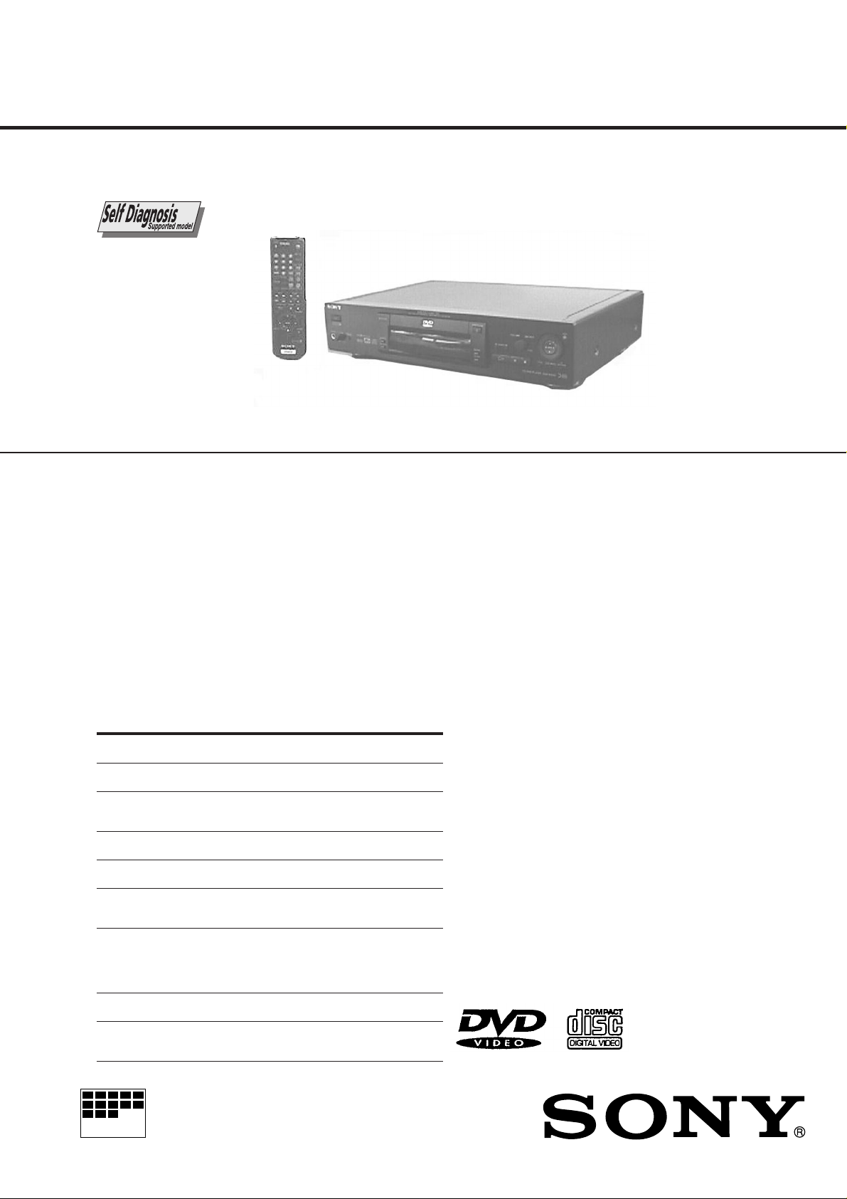
DVP-S533D
RMT-D108A
SERVICE MANUAL
SPECIFICATIONS
CD/DVD player
Laser Semiconductor laser
Signal format system NTSC
Audio characteristics
Frequency response DVD (PCM 96 kHz): 2 Hz to 44 kHz
(±1 dB)*
DVD (PCM 48 kHz): 2 Hz to 22 kHz
(±0.5 dB)
CD: 2 Hz to 20 kHz (±0.5 dB)
Signal-to-noise ratio More than 115 dB (LINE OUT (AUDIO 1,
2) connectors only)
Harmonic distortion Less than 0.0025%
Dynamic range More than 100 dB (DVD)
More than 97 dB (CD)
Wow and flutter Less than detected value
(±0.001% W PEAK)
Outputs and inputs
Jack Output Load impedance
type level
LINE OUT Phono 2 Vrms Over 10 kilohms
(AUDIO 1, 2) jacks (at 50 kilohms)
DIGITAL OUT Optical –18 dBm Wave length: 660 nm
(OPTICAL) output
connector
DIGITAL OUT Phono 0.5 Vp-p 75 ohms terminated
(COAXIAL) jack
LINE OUT Phono 1.0 Vp-p 75 ohms,
(VIDEO 1, 2) jacks sync negative
S VIDEO OUT 4-pin Y: 1.0 Vp-p 75 ohms,
(1, 2) mini DIN sync negative
C: 0.286 Vp-p 75 ohms terminated
COMPONENT phono Y: 1.0 Vp-p 75 ohms,
VIDEO OUT jacks sync negative
(Y, PB/B-Y, PB/B-Y,
PR/R-Y) PR/R-Y:
0.7 Vp-p 75 ohms
PHONES Phone 12 mW 32 ohms
jack
5.1CH Phono 2 Vrms Over 10 kilohms
OUTPUT jacks (at 50 kilohms)
PX Model
General
Power requirements 110 to 240 V AC, 50/60 Hz
Power consumption 16 W
Dimensions (approx.) 430 × 95 × 305 mm
(17 × 33/4 × 12 in.) (w/h/d)
incl. projecting parts
Mass (approx.) 3.4 kg (7 lb 8 oz)
Operating temperature 41°F to 95°F (5°C to 35°C)
Operating humidity 5% to 90%
Supplied accessories
• Audio/Video/S-link connecting cord (1)
• S video cable (1)
• Plug adaptor (1)
• Remote commander (remote) RMT-D108A (1)
• Size AA (R6) batteries (2)
* The signals from LINE OUT (AUDIO 1, 2) connectors and 5.1 ch L, R
connectors are measured. When you play the PCM sound tracks with
96 kHz sampling frequency, the output signals from the DIGITAL OUT
(OPTICAL, COAXIAL) are converted to 48 kHz (sampling frequency).
Design and specifications are subject to change without notice.
CD/DVD PLAYER
MICROFILM
Page 2
SAFETY CHECK-OUT
After correcting the original service problem, perform the following
safety checks before releasing the set to the customer:
1. Check the area of your repair for unsoldered or poorly-soldered connections. Check the entire board surface for solder
splashes and bridges.
2. Check the interboard wiring to ensure that no wires are
“pinched” or contact high-wattage resistors.
3. Look for unauthorized replacement parts, particularly transistors, that were installed during a previous repair. Point them
out to the customer and recommend their replacement.
4. Look for parts which, though functioning, show obvious signs
of deterioration. Point them out to the customer and recommend their replacement.
5. Check the line cord for cracks and abrasion. Recommend the
replacement of any such line cord to the customer.
6. Check the B+ voltage to see it is at the values specified.
7. Check the antenna terminals, metal trim, “metallized” knobs,
screws, and all other exposed metal parts for AC leakage.
Check leakage as described below.
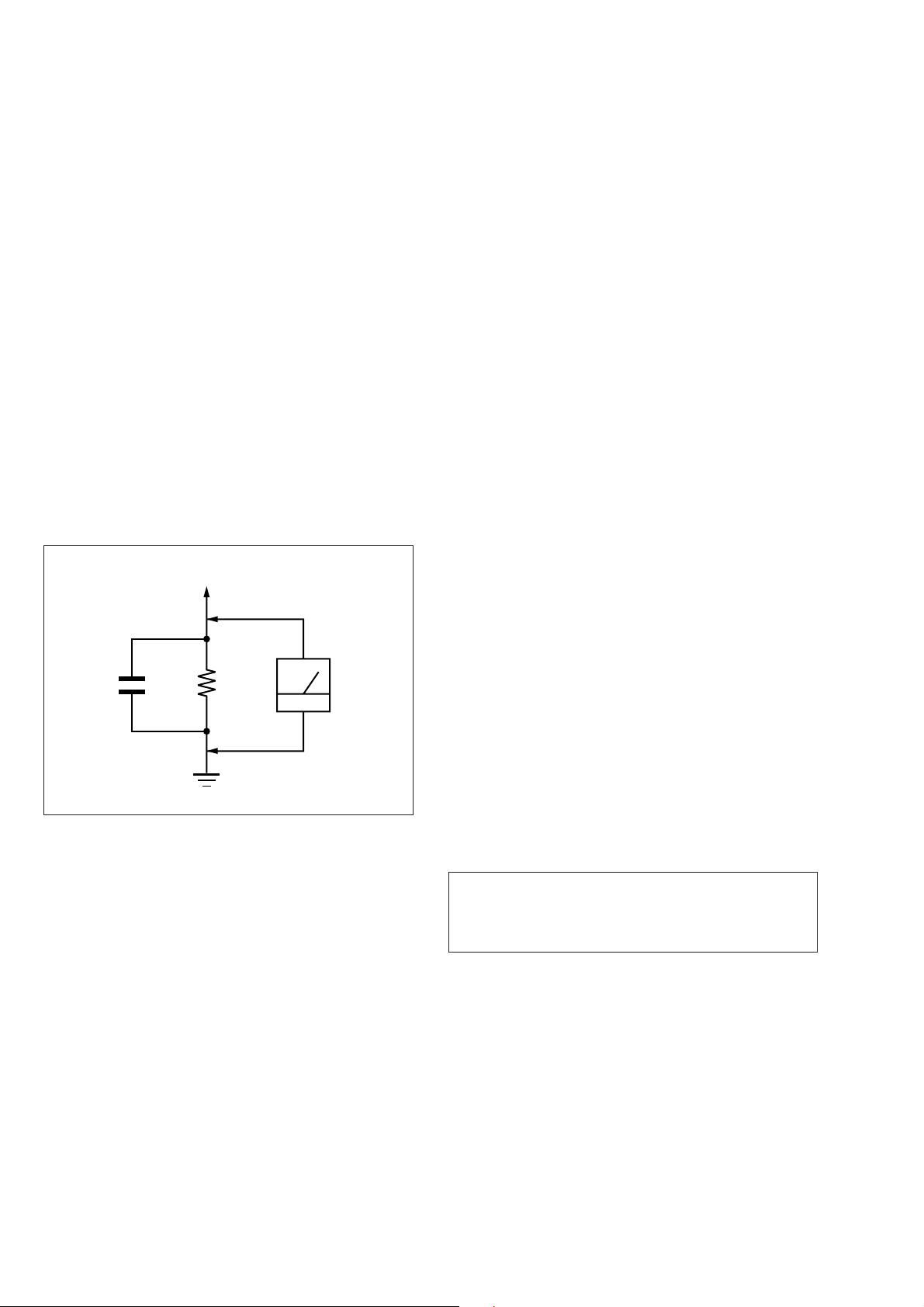
To Exposed Metal
Parts on Set
LEAKAGE TEST
The AC leakage from any exposed metal part to earth ground
and from all exposed metal parts to any exposed metal part having
a return to chassis, must not exceed 0.5 mA (500 microamperes).
Leakage current can be measured by any one of three methods.
1. A commercial leakage tester, such as the Simpson 229 or RCA
WT -540A. Follow the manufacturers' instructions to use these
instruments.
2. A battery-operated A C milliammeter. The Data Precision 245
digital multimeter is suitable for this job.
3. Measuring the voltage drop across a resistor by means of a
VOM or battery-operated AC voltmeter. The “limit” indica-
tion is 0.75V, so analog meters must have an accurate low-
voltage scale. The Simpson 250 and Sanwa SH-63T rd are e x-
amples of a passive VOM that is suitable. Nearly all battery
operated digital multimeters that have a 2V A C range ar e suit-
able. (See Fig. A)
AC
0.15 µF
1.5 k
Ω
Earth Ground
Voltmeter
(0.75 V)
Fig. A Using AC voltmeter to check AC leakage
WARNING!!
WHEN SERVICING, DO NO T APPR O A CH THE LASER
EXIT WITH THE EYE TOO CLOSELY. IN CASE IT IS
NECESSARY TO CONFIRM LASER BEAM EMISSION,
BE SURE TO OBSERVE FROM A DISTANCE OF
MORE THAN 25 cm FROM THE SURFACE OF THE
OBJECTIVE LENS ON THE OPTICAL PICK-UP BLOCK.
CAUTION:
The use of optical instrument with this product will increase eye
hazard.
CAUTION
Use of controls or adjustments or performance of procedures
other than those specified herein may result in hazardous radiation exposure.
SAFETY-RELATED COMPONENT WARNING!!
COMPONENTS IDENTIFIED BY MARK ! OR DOTTED
LINE WITH MARK ! ON THE SCHEMA TIC DIAGRAMS
AND IN THE PARTS LIST ARE CRITICAL TO SAFE
OPERATION. REPLACE THESE COMPONENTS WITH
SONY PARTS WHOSE PART NUMBERS APPEAR AS
SHOWN IN THIS MANUAL OR IN SUPPLEMENTS PUBLISHED BY SONY.
– 2 –
Page 3

TABLE OF CONTENTS
Section Title Page Section Title Page
Service Note ............................................................................ 4
1. GENERAL
This Player Can Play the Following Discs.................... 1-1
Getting Started .............................................................. 1-1
Playing Discs................................................................. 1-3
Using Various Functions with the Control Menu........... 1-5
Settings and Adjustments ............................................. 1-10
Additional Information ................................................... 1-13
SW-317 (SURROUND SWITCH), FR-150
(IR/POWER SWITCH) Printed Wiring Boards.............. 4-52
SW-317 (SURROUND SWITCH), FR-150
(IR/POWER SWITCH) Schematic Diagram ................. 4-53
HS-030SF (SWITCHING REGULATOR)
Printed Wiring Board ..................................................... 4-55
HS-030SF (SWITCHING REGULATOR)
Schematic Diagram....................................................... 4-57
5. IC PIN FUNCTION DESCRIPTION
2. DISASSEMBLY
2-1. Case Removal ............................................................... 2-1
2-2. MB-85 Board Removal .................................................. 2-1
2-3. Power Block Removal ................................................... 2-1
2-4. AU-212 Board Removal ................................................ 2-1
2-5. Tray Cover Removal ..................................................... 2-2
2-6. Front Panel Removal .................................................... 2-2
2-7. Mechanism Deck Removal ........................................... 2-2
2-8. Tray Removal ................................................................ 2-2
2-9. Optical Pick-up Removal............................................... 2-3
2-10. Belt, Loading Motor (M001),
MS-46, TK-51 Board Removal...................................... 2-3
2-11. Internal View.................................................................. 2-4
2-12. Circuit Boards Location................................................. 2-5
3. BLOCK DIAGRAMS
3-1. Overall Block Diagram .................................................. 3-1
3-2. RF/Servo Block Diagram .............................................. 3-3
3-3. Signal Process/Video Block Diagram ........................... 3-5
3-4. System Control Block Diagram ..................................... 3-7
3-5. Audio (1) Block Diagram ............................................... 3-9
3-6. Audio (2) Block Diagram ............................................... 3-11
3-7. Interface Control Block Diagram................................... 3-13
3-8. Power Block Diagram.................................................... 3-15
4. PRINTED WIRING BOARDS AND SCHEMATIC
DIAGRAMS
4-1. Frame Schematic Diagram ........................................... 4-3
4-2. Printed Wiring Boards and Schematic Diagrams ......... 4-7
TK-51 (RF/SERVO) Printed Wiring Board.................... 4-7
TK-51 (RF/SERVO) Schematic Diagram...................... 4-11
MS-46 (LOADING) Printed Wiring Board and
Schematic Diagram....................................................... 4-13
MB-85 (SIGNAL PROCESS/SERVO)
Printed Wiring Board ..................................................... 4-15
MB-85 (AV DECODER) Schematic Diagram................ 4-19
MB-85 (SDRAM) Schematic Diagram .......................... 4-21
MB-85 (SERVO DSP) Schematic Diagram .................. 4-23
MB-85 (DRIVE) Schematic Diagram ............................ 4-25
MB-85 (ARP) Schematic Diagram ................................ 4-27
MB-85 (SYSTEM CONTROL) Schematic Diagram...... 4-29
MB-85 (HGA) Schematic Diagram................................ 4-31
MB-85 (CLOCK GENERATOR, AUDIO DSP)
Schematic Diagram....................................................... 4-33
MB-85 (DAC) Schematic Diagram ................................ 4-35
MB-85 (BIAS) Schematic Diagram ............................... 4-37
AU-212 (AUDIO, VIDEO BUFFER)
Printed Wiring Board ..................................................... 4-39
AU-212 (AUDIO) Schematic Diagram .......................... 4-41
AU-212 (VIDEO BUFFER) Schematic Diagram........... 4-43
FL-101 (FUNCTION SWITCH, IF CON)
Printed Wiring Board ..................................................... 4-45
FL-101 (FUNCTION SWITCH) Schematic Diagram .... 4-47
FL-101 (IF CON) Schematic Diagram .......................... 4-49
HP-111 (HEADPHONE) Printed Wiring Board
and Schematic Diagram................................................ 4-51
5-1. System Control Pin Function
(MB-85 Board IC202) .................................................... 5-1
6. TEST MODE
6-1. General Description ...................................................... 6-1
6-2. Starting Test Mode ........................................................ 6-1
6-3. Syscon Diagnosis.......................................................... 6-1
6-4. Drive Auto Adjustment................................................... 6-5
6-5. Drive Manual Operation ................................................ 6-7
6-6. Mecha Aging.................................................................. 6-9
6-7. Emergency History ........................................................ 6-9
6-8. Version Information ....................................................... 6-10
6-9. Video Level Adjustment................................................. 6-10
7. ELECTRICAL ADJUSTMENTS
7-1. Power Supply Adjustment ............................................. 7-1
1. Power Supply Check (HS-030SF BOARD) .................. 7-1
7-2. Adjustment of Video System......................................... 7 - 2
1. Video Level Adjustment (MB-85 BOARD) .................... 7-2
2. S-terminal Output Check (MB-85 BOARD) .................. 7-2
3. Checking Component Video Output B-Y
(MB-85 BOARD)............................................................ 7-2
4. Checking Component Video Output R-Y
(MB-85 BOARD)............................................................ 7-2
5. Checking Component Video Output Y
(MB-85 BOARD)............................................................ 7-3
6. Checking S Video Output S-C (MB-85 BOARD) .......... 7-3
7-3. Adjustment Related Parts Arrangement ....................... 7-4
8. REPAIR PARTS LIST
8-1. Exploded Views ............................................................. 8-1
8-1-1. Case Assembly......................................................... 8-1
8-1-2. Front Panel Assembly .............................................. 8-2
8-1-3. Chassis Assembly .................................................... 8-3
8-1-4. Mechanism Deck Assembly..................................... 8-4
8-2. Electrical Parts List........................................................ 8-5
– 3 –
Page 4
SERVICE NOTE
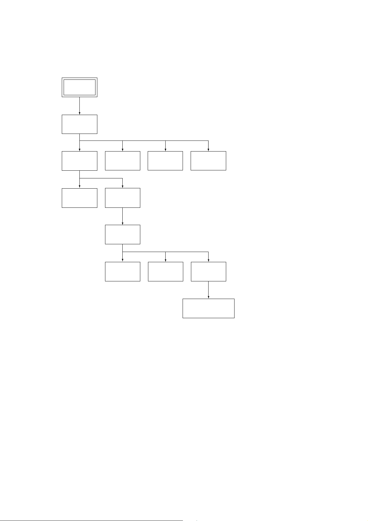
1. DISASSEMBLY
• This set can be disassembled in the order shown below.
Set
Case
(Page 2-1)
Tray Cover
(Page 2-2)
Front Panel
(Page 2-2)
MB-85 Board
(Page 2-1)
Mechanism
Deck
(Page 2-2)
Tray
(Page 2-2)
Optical Pick-up
(Page 2-3)
AU-212 Board
(Page 2-1)
TK-51 Board
(Page 2-3)
Power
Block
(Page 2-1)
Belt
(Page 2-3)
Loading Motor (M001),
MS-46 Board
(Page 2-3)
– 4 –
Page 5
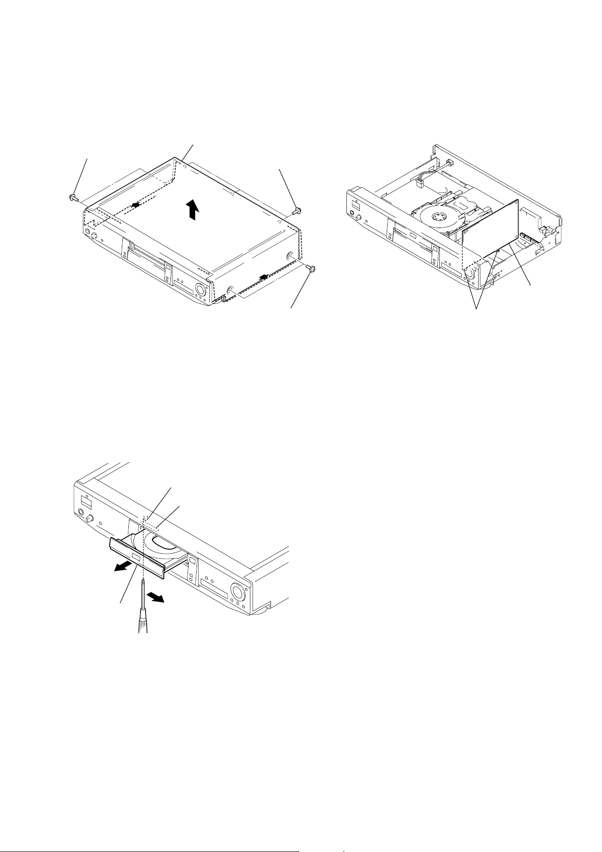
2. NOTE ON REMOVE THE CASE
1) Remove seven screws. (See Fig. 1)
2) Open the side of case. (See Fig. 1)
3) Remove the case as lift straight. (See Fig. 1)
Case
Two screws
Three screws
4. HOW TO SERVICE MB-85 BOARD
1) Remove the case from the set. (Refer to 2-1)
2) Remove the MB-85 board. (Refer to 2-2)
3) Set the MB-85 board as shown in Fig. 3.
Note: Do not disconnect wiring, except FMA-7/8/9.
MB-85 board
Two screws
Fig. 1
3. DISC REMOVAL PROCEDURE
(at POWER OFF)
1) Insert a tapering driver into the aperture of the unit bottom,
and move the lever of chuck cam in the direction of the arrow
A. (See Fig. 2)
2) Draw out the tray in the direction of the arrow B, and remove
a disc. (See Fig. 2)
Lever of chuck cam
Aperture
B
A
Tray
grooves
Fig. 3
Fig. 2
– 5 –
Page 6
SECTION 1
GENERAL
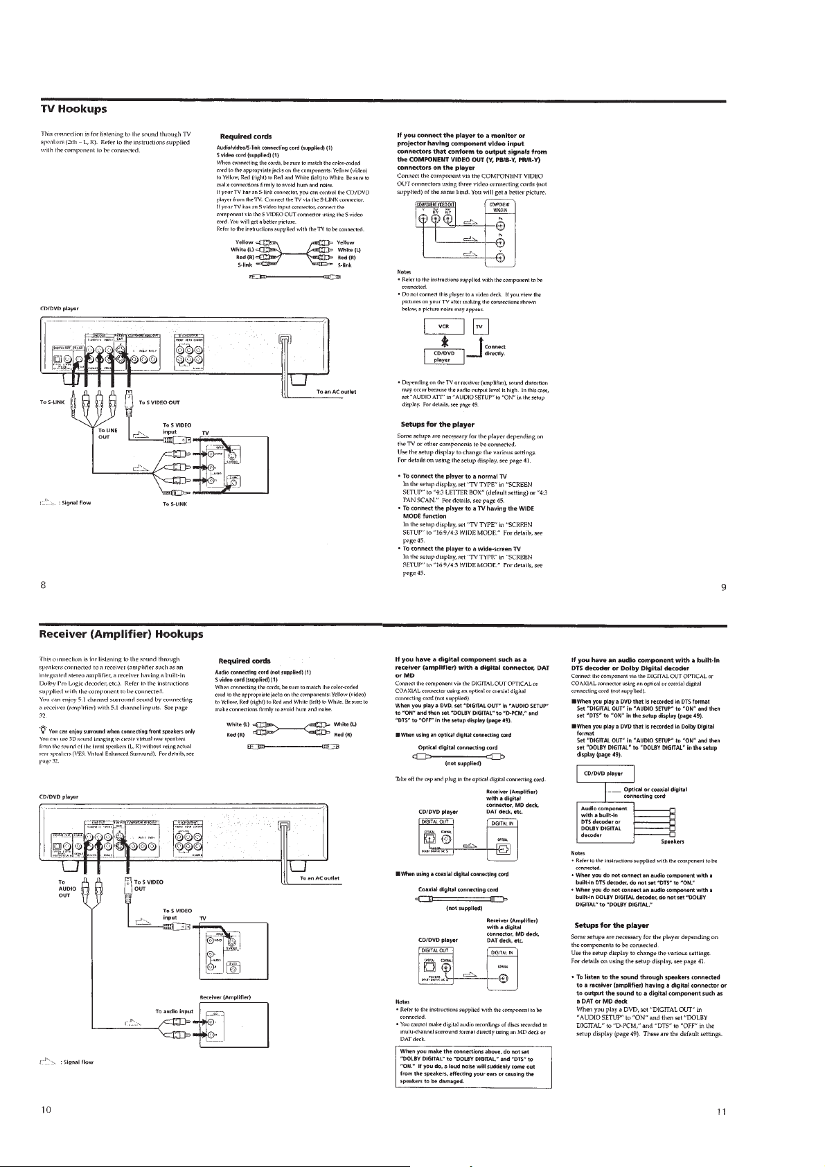
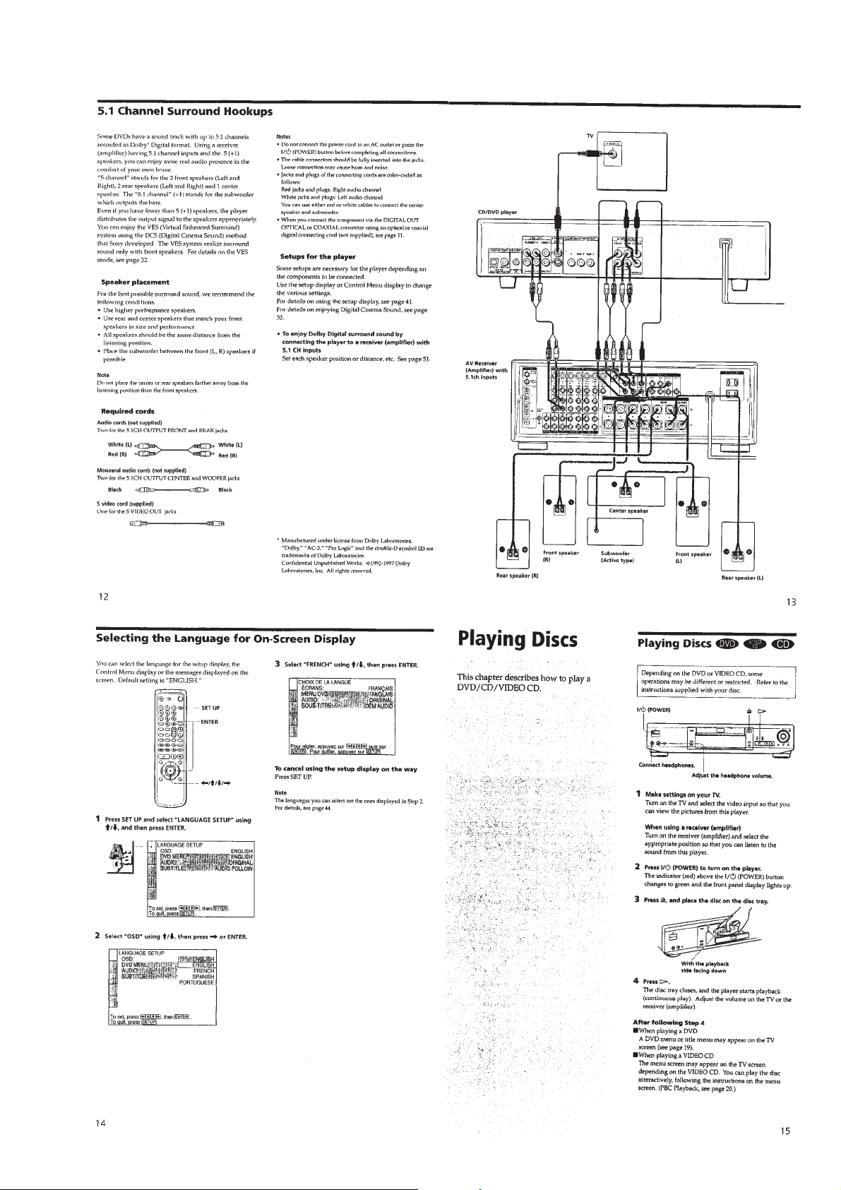
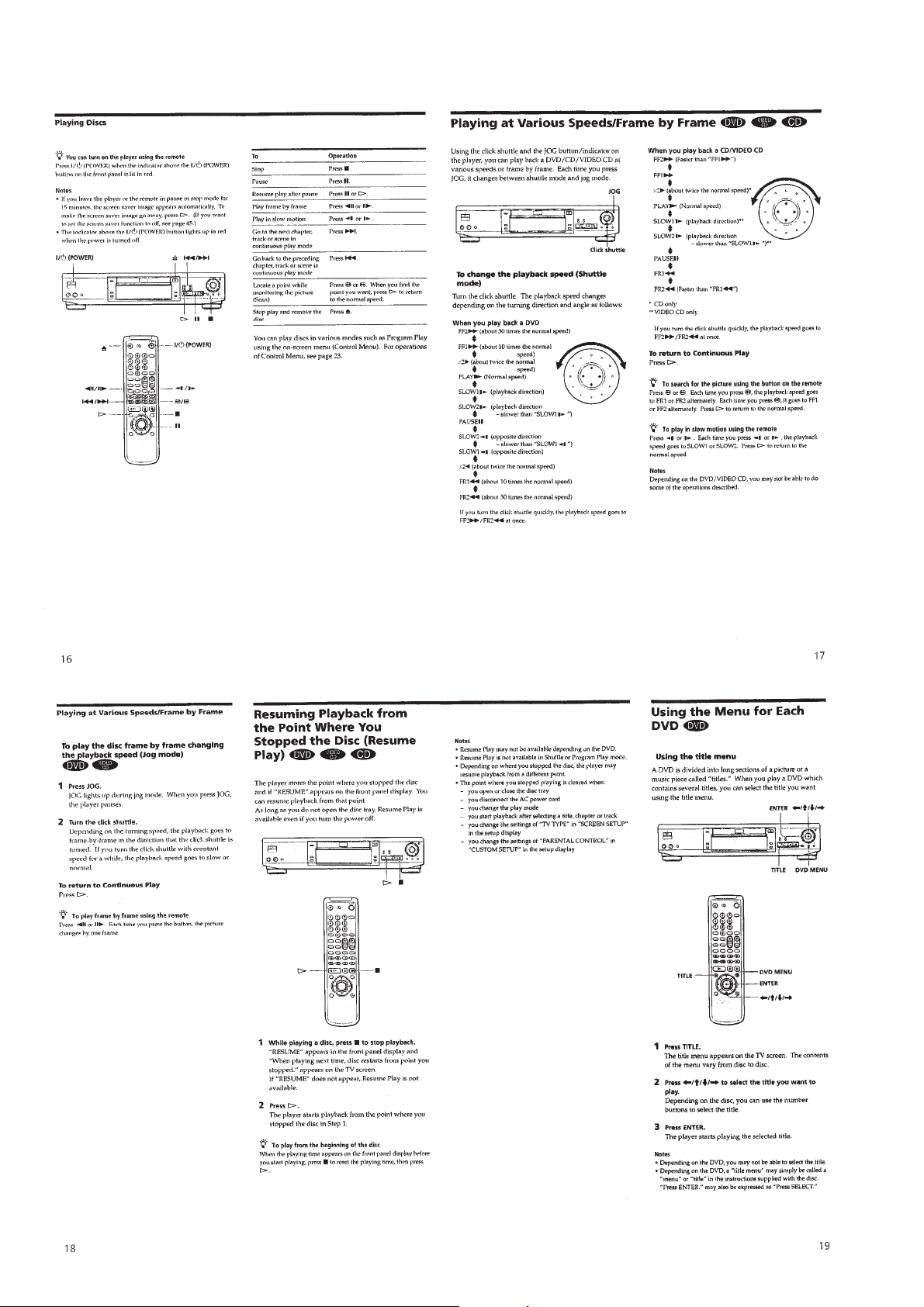
DVP-S533D
This section is extracted from instruction manual (3-867-038-11).
1-1
Page 7
1-2
Page 8
1-3
Page 9
1-4
Page 10
1-5
Page 11
1-6
Page 12
1-7
Page 13
1-8
Page 14
1-9
Page 15
1-10
Page 16
1-11
Page 17
1-12
Page 18
1-13
Page 19
1-14 E
1-14
Page 20
SECTION 2
1 Connector
(CN101)
2 Three connectors
(CN201, 202, 203)
3 Four screws
(B3)
4 Power block
DISASSEMBLY
Note: Follow the disassembly procedure in the numerical order given.
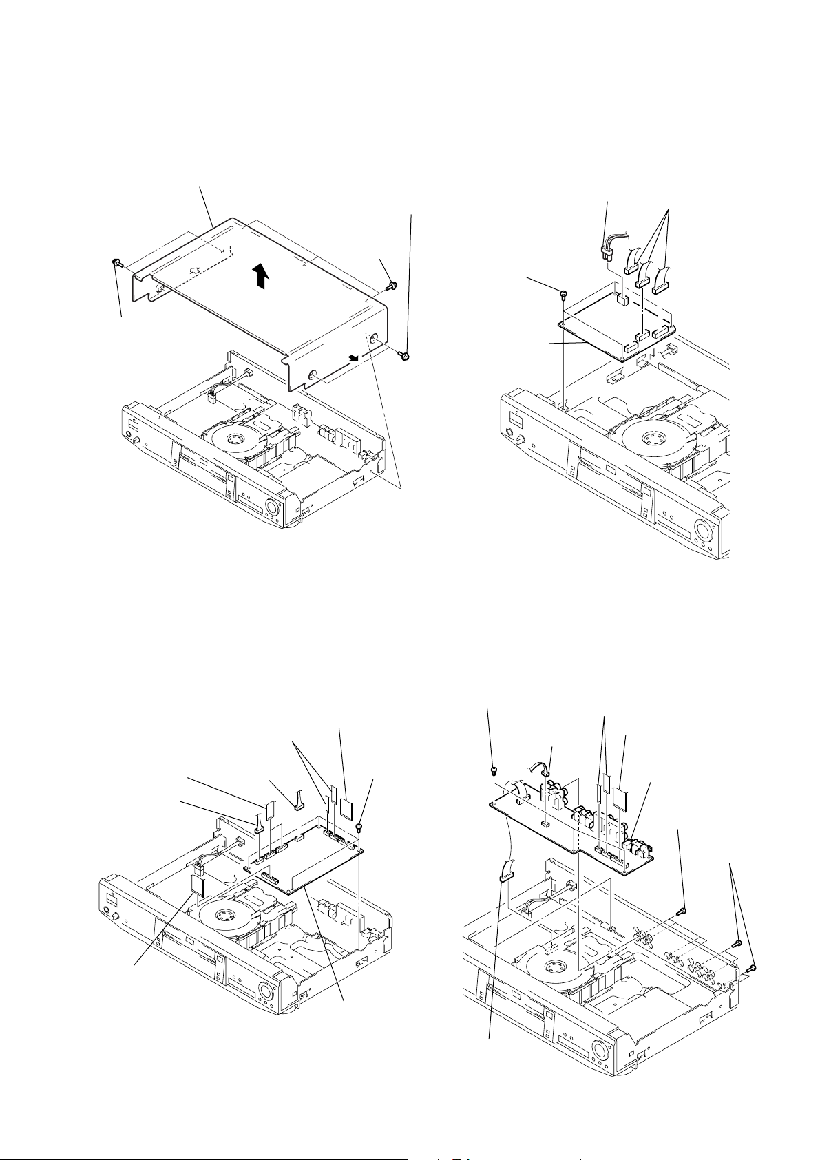
2-1. CASE REMOVAL 2-3. POWER BLOCK REMOVAL
4 Case
2 Two screws
1 Three screws
3 Two screws
DVP-S533D
2-2. MB-85 BOARD REMOVAL
5 Flat cable
2 Two flat cables
(CN002, 003)
1 Connector
(CN011)
6 Flat cable
(CN006)
4 Two flat cables
(CN004, 007)
3 Connector
(CN001)
(CN005)
7 Four screws
(B3)
8 MB-85 board
2-4. AU-212 BOARD REMOVAL
7 Three screws
(B3)
2 Connector
1 Connector
(CN201)
3 Two flat cables
(CN302, 303)
(CN401)
4 Flat cable
(CN301)
8 AU-212 board
5 Four screws
(B3)
6 Four screws
(B3)
2-1
Page 21
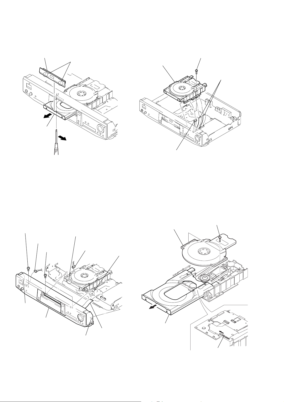
2-5. TRAY COVER REMOVAL 2-7. MECHANISM DECK REMOVAL
4 Tray cover
3 Two claws
B
2 Pull the tray in the
direction of the
arrow B.
A
1 Insert a tapering driver into the aperture of the
unit bottom, and move the lever of chuck cam
in the direction of the arrow A.
4 Mechanism deck
1 Connector
(CN001)
3 Screw
(B3)
2 Two flat cables
(CN003, 004)
2-6. FRONT PANEL REMOVAL
4 Screw
(B3)
2 Connector
(CN701)
5 Two screws
(B3)
9 Claw
!º Front panel
6 Boss
1 Connector
8 Claw
(CN203)
3 Flat cable
(CN006)
7 Boss
2-8. TRAY REMOVAL
2 Chuck ass’y
B
4 Remove the tray in
the direction of the
arrow B.
1 Two screws
(BTP2.6 × 12)
A
2-2
3 Move the lever of chuck cam
in the direction of the arrow A.
Page 22
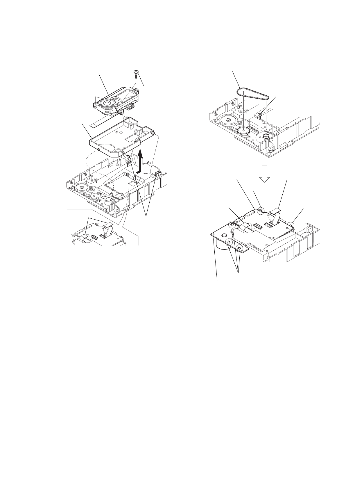
2-9. OPTICAL PICK-UP REMOVAL 2-10. BELT, LO ADING MOTOR (M001),
MS-46, TK-51 BOARD REMOVAL
5 Optical pick-up
3 Remove the base
unit holder in the
direction of the
arrow A.
1 Two flexible board
(CN001, 002)
4 Three step
screws
A
2 Two claws
1 Belt
9 TK-51 board
5 Flexible board
(CN002)
2 Two screws
(B2.6 × 4)
6 Flexible board
(CN001)
8 Claw
7 Claw
3 Three claws
4 Loading motor (M001),
MS-46 board
2-3
Page 23
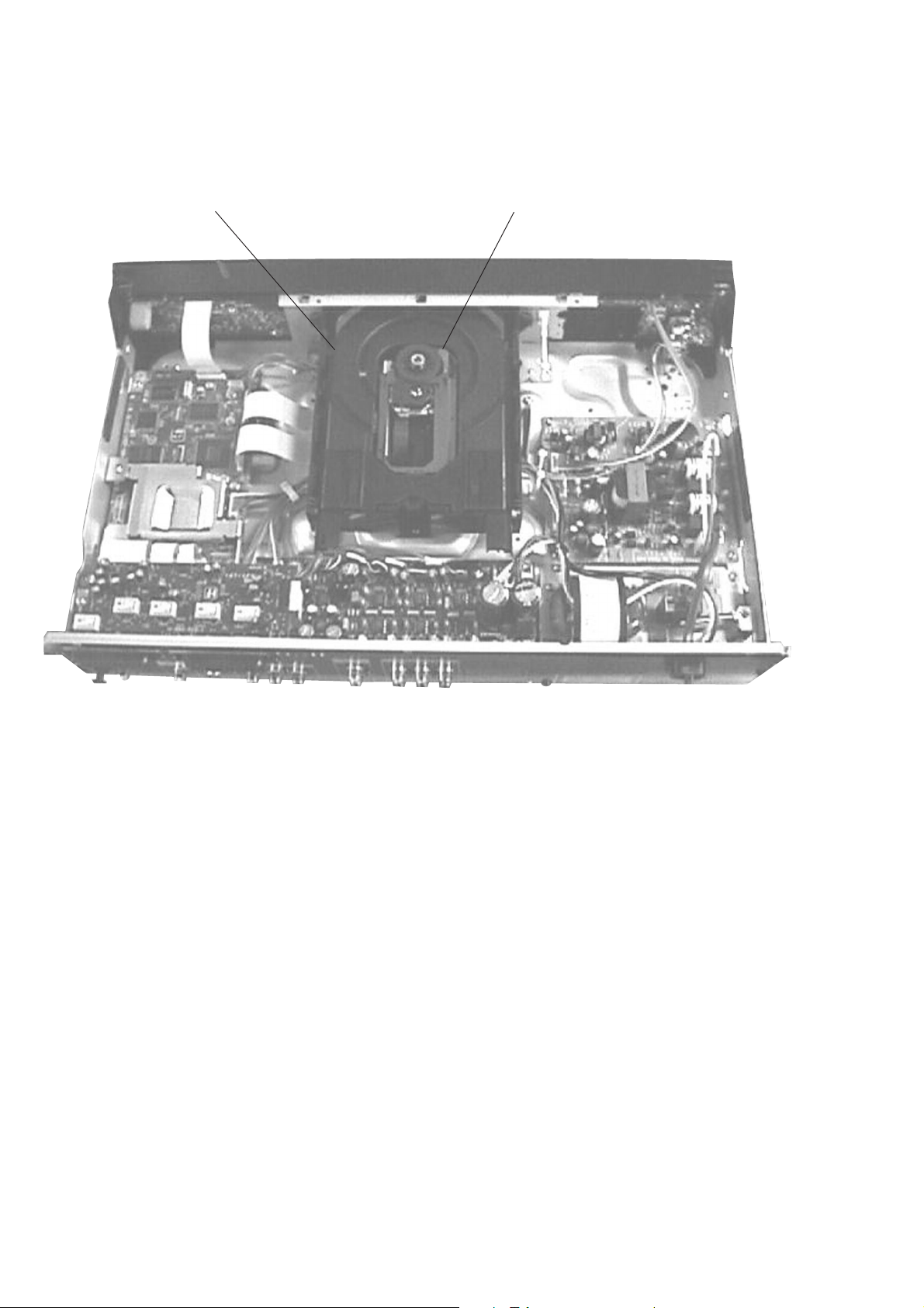
2-11. INTERNAL VIEW
DC motor (loading)
1-541-632-11
Optical pick-up (KHM-220AAA/J1RP)
8-820-081-03
2-4
Page 24
2-12. CIRCUIT BOARDS LOCATION
Power Block (HS-030SF)
(SWITCHING REGULATOR)
FR-150
(IR/POWER SWITCH)
HP-111
(HEADPHONE)
SW-317
(SURROUND SWITCH)
MS-46
(LOADING)
TK-51
(RF/SERVO)
FL-101
(FUNCTION SWITCH)
AU-212
(AUDIO)
MB-85
(SIGNAL PROCESS/SERVO)
2-52-5 E
Page 25
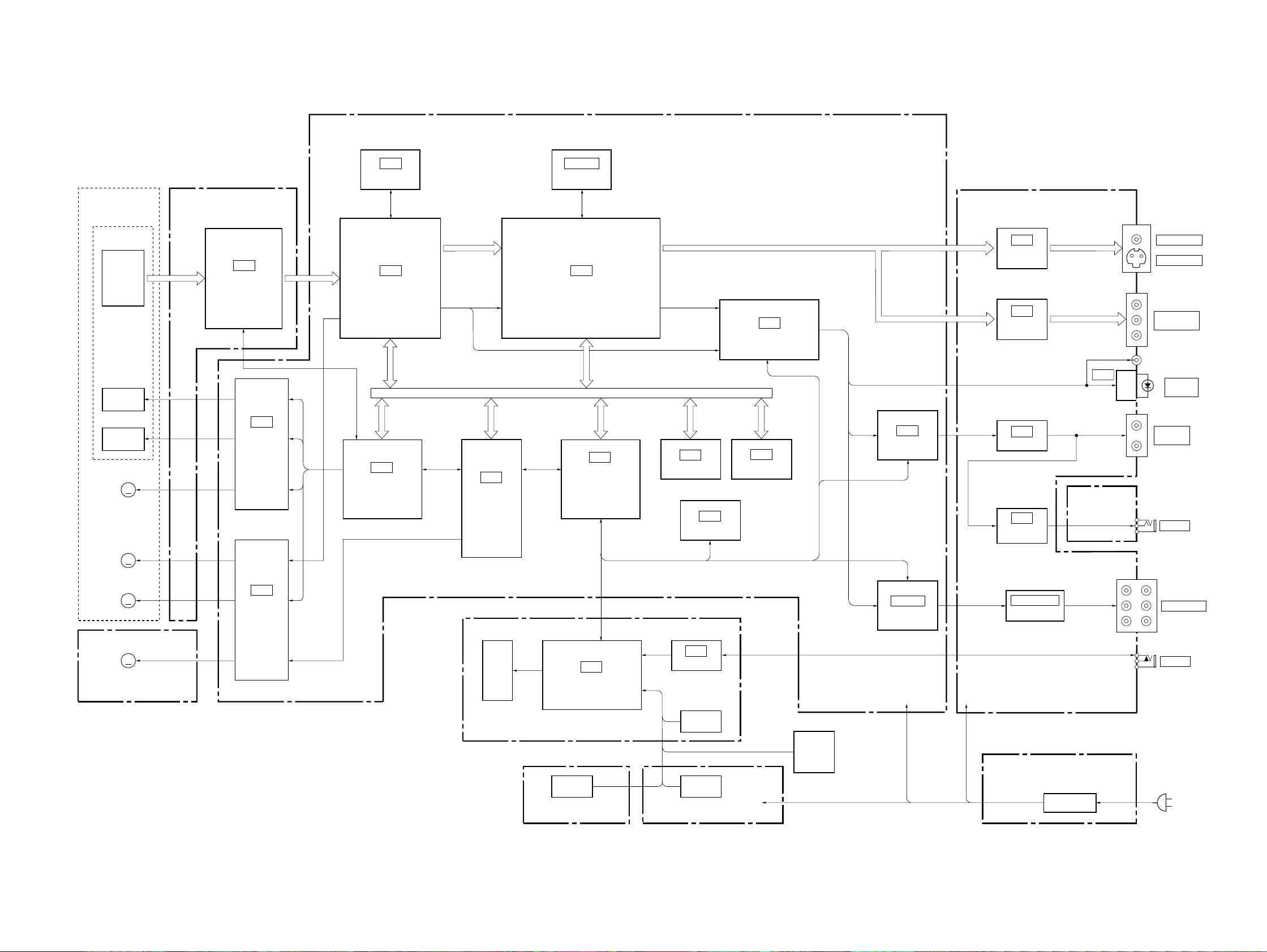
3-1. OVERALL BLOCK DIAGRAM
SECTION 3
BLOCK DIAGRAMS
MB-85 BOARD
(SEE PAGE 4-19 to 37)
DVP-S533D
BASE UNIT
KHM-220AAA
OPTICAL DEVICE
DVD/CD
FOCUS
TRACKING
TILT
MOTOR
SPINDLE
MOTOR
PDIC
COIL
COIL
IC304
16M DRAM
TK-51 BOARD
(SEE PAGE 4-11)
SD 0-7
RF
IC001
DVD/CD RF AMP
DIGITAL SERVO
IC801
FOCUS COIL/
TRACKING COIL/
TILT MOTOR
DRIVE
M
DVD RF,
CD RF
IC303
ARP2
IC701
SERVO DSP
CDDOUT, CDDATA,
CDBCK, CDLRCK
IC601
HGA
M
IC402, 403
16M SDRAM
IC401
AV DECODER
IC202
SYSTEM CONTROL
Parallel BUS
Serial BUS
ACH12,
ACH34, ACH56,
BCK, LRCK
IC204
1M SRAM
4K EEP ROM
IC201
IC501
AUDIO DSP
IC206
16M FLASH
VIDEO V,
VIDEO Y,
VIDEO C
VIDEO G/Y,
VIDEO R/B-Y,
VIDEO B/R-Y
SPDIF
IC902
AUDIO 2CH DAC
AU-212 BOARD
(SEE PAGE 4-41, 43)
AUDIO LT,
AUDIO RT
HEADPHONE
IC321
VIDEO
BUFFER
IC303
VIDEO
BUFFER
IC431
LPF
IC401
AMP
IC505
HP-111 BOARD
(SEE PAGE 4-51)
VIDEO 1, 2
S VIDEO 1, 2
COMPONENT
VIDEO
DIGITAL
OUT
AUDIO
OUT1, 2
PHONES
SLED
M
MOTOR
M001
LOADING
05
M
MOTOR
MS-46 BOARD
(SEE PAGE 4-14)
IC802
SPINDLE/SLED/
LOADING
MOTOR DRIVE
ND201
FL-101 BOARD
(SEE PAGE 4-47, 49)
SW-317 BOARD
(SEE PAGE 4-53)
IC203
IC201
IF CON
SWITCH SWITCH
S-LINK
SWITCH
FR-150 BOARD
(SEE PAGE 4-53)
–12V
EVER5V
JOG UNIT
IC905-907
AUDIO 5.1CH DAC
+3.3V
+5V
A+12V
M+12V
AUDIO L, R
AUDIO LS, RS
AUDIO C, LFE
+3.3V
+5V
+12V
–12V
EVER5V
HS-030SF BOARD
(SEE PAGE 4-57)
IC502, 541, 571
LPF
5.1CH OUTPUT
S-LINK
SW REG
3-1 3-2
Page 26
DVP-S533D
3-2. RF/SERVO BLOCK DIAGRAM
BASE UNIT
KHM-220AAA
OPTICAL DEVICE
DVD/CD
PDIC
DVD/CD
LD MODULE
COIL
TRACKING
COIL
TILT
M
MOTOR
INLIMIT
SENSOR
RF
A-D
E-H
VC
PD
LD
VR
FCSFOCUS
TRK
TIA, TIB
INLIM
TK-51 BOARD
IC0011(DVD play)
200mV/DIV 100ns/DIV
536mVp-p
IC0011(CD play)
500mV/DIV 500ns/DIV
880mVp-p
CN001
7
9
10
16
17
8
11
15
18
13
4
2
5
19
20
21
22
CN002
10
ı
13
2
Q001
LD DRIVE
(SEE PAGE 4-11)
IC001
DVD/CD RF AMP
DIGITAL SERVO
RF IP
1 54
9
ı
A-D
12
5
ı
A2-D2
8
13
E-H
ı
16
VC
17
19
PD
20
LD
IC001@ª(DVD play)
200mV/DIV 500ms/DIV
592mVp-p
IC001%¢(DVD play)
500mV/DIV 100ns/DIV
1.5Vp-p
IC001%¢(CD play)
500mV/DIV 500ns/DIV
1.5Vp-p
SIGO
40
FE
39
TE
29
PI
26
MIRR
32
TZC
33
VCI
SCLK
43
SWD
ı
SRD
46
SDEN
27
FDCHG
42
HOLD2
31
DFT
IC001@ª(CD play)
200mV/DIV 20ms/DIV
448mVp-p
Q002
CN004
17
9
8
7
3
5
6
11
ı
14
15
4
6
7
4
5
15
ı
18
8
RF+
FE
TE
PI
MIRR
TZC
2VC
SSCK, SSWD,
SSRD, SSCS
SSDFCT
SSDFCTI
FCS
TRK
TIA, TIB
INLIM
MB-85 BOARD(1/6)
IC001$º(DVD play)
100mV/DIV 50ms/DIV
180mVp-p
500mV/DIV 50ms/DIV
CN002CN003
2
10
11
12
16
14
2VC
13
5
ı
8
4
15
CN003
12
13
14
15
1
ı
4
11
(SEE PAGE 4-23, 25)
500mV/DIV 50ms/DIV
IC001#ª(DVD play)
1.3Vp-p
IC001$º(CD play)
860mVp-p
IC001#ª(CD play)
500mV/DIV 200ms/DIV
13
14
TRACKING
11
12
15
ı
18
1.7Vp-p
IC801
FOCUS
COIL
DRIVE
COIL
DRIVE
TILT
MOTOR
DRIVE
IC802
20
23
26
2
3
9
5
6
7
FCD
TRD
TLTA, TLTB
Q801
IC702 (1/2)
3 1
IC803 (1/2)
12
13
IC701^ª(DVD play)
500mV/DIV 50ms/DIV
1.4Vp-p
IC701^ª(CD play)
500mV/DIV 200ms/DIV
1.7Vp-p
14
IC701^•(DVD play)
100mV/DIV 5ms/DIV
IC701^•(CD play)
500mV/DIV 50ms/DIV
FCD
TRD
TLTA,TLTB
SLDA, SLDB,
STVC
TILT MUTE
FGMODE
180mVp-p
860mVp-p
68
ADC1
69
ADC0
67
ADC2
66
ADC3
65
ADC4
21
TRIN
20
TRREF
23
FGIN
41
GIO 5-8
ı
44
38
GIO 11
28
DFCTI
80
DAB 2,3
85
92
DAB 0, 1
97
48
GIO 1, 2
49
7
PWM 0-2
ı
9
46
GIO 4
50
GIO 0
IC701
SERVO DSP
RS
26 108
X2/CLKIN
FG REF
VRBA,
VRB 0-3
GIO 10
HINT
HRD
HWR
HCS
EA 0, 1
HD 0-7
DVD RF
CD RF
SIGNAL PROCESS,
22
74
81
84
93
96
39
128
1
2
3
4
5
117
ı
120
122
ı
125
IC702 (2/2)
7 5
LOCK
MDS0
MDP0
+3.3V
FCSON
XSDPIT
XSDPRD
XSDPWR
XSDPCS
HA0, 1
HD8-15
N27MSDP
XSDPRST
X3VRST
VIDEO
(SEE PAGE 3-5)
SYSTEM
CONTROL
(SEE PAGE 3-7,8)
SPINDLE
8
SPINDLE
M
MOTOR
SLED
M
MOTOR
05
SPM
SLA, SLB
9
4
ı
7
MS-46 BOARD
(SEE PAGE 4-14)
M001
LOADING
M
MOTOR
S001
TRAY SENSOR
S002
CHUCK SENSOR
CN001
13
14
12
9
ı
1
2
4
6
3
SPM
SLA, SLB
LDM
OCSW 1, 2
CKSW1
5
6
7
ı
10
1
2
4
6
3
CN011
OCSW 1, 2
CKSW1
15
MOTOR
16
DRIVE
SLED
11
ı
MOTOR
14
DRIVE
LOADING
17
MOTOR
18
DRIVE
26
20
2
3
5
6
9
23
SLDA, SLDB,
STVC
+3.3V
+5V
IC803 (2/2)
5 7
10
3 1
2.5VC
8
2VC
1.6VC
Q802, 803
GAIN
CONTROL
SPDLSTOP
SPGAIN
XDRV MUTE
LDMM/DMM
LDMP/DMP
OCSW1
OCSW2
CKSW1
3-3 3-4
Page 27
3-3. SIGNAL PROCESS/VIDEO BLOCK DIAGRAM
MB-85 BOARD(2/6)
(SEE PAGE 4-19, 21, 27, 35)
IC303!¶(DVD play)
500mV/DIV 200ns/DIV
RF, SERVO
(SEE PAGE 3-4)
SYSTEM
CONTROL
(SEE PAGE 3-7,8)
IC303!ª(CD play)
1.6Vp-p
DVD RF
CD RF
MDS0
MDP0
LOCK
DFCT
NORF
LOCK
FWON
MD2
MUTE
XARPWR
XARPRD
XARPIT
XARPCS
XARPWT
XCS2
XCS3
XRD
XWRH
XAVDIT
XAVDWT
DACK0
DREQ0
DACK1
DREQ1
500mV/DIV 100ns/DIV
1.6Vp-p
136-139
141-144
RFIN1
RFIN2
MDS0
MDP0
DFCT
NORF
LOCK
FWON
MD2
MUTE
XWR
XRD
XINT
XCS
XWAT
XRST
87
121
XARPRST
33MARP
146 147
MCKI
123
17
19
49
52
55
56
58
59
113
111
60
61
83
84
86
MA 0-9
SCKI
IC304
16M DRAM
MD 00-15
154-157
159-162
164-167
169-172
IC303
ARP2
A 0-7
73-76 79-82
XRAS, XOE
XMWR, XCAS,
148
150-152
63-68 70 71
SD 0-7
D 0-7
97
SD 0-7
98
100
ı
105
SDCK, SDEF,
91
XSHD, XSAK, XSRQ
93
ı
96
CDDOUT, CDDATA,
107
CDBCK, CDLRCK
ı
110
DVP-S533D
IC402, 403
16M SDRAM
IC401%•
DDT 0-15
DAD 0-11
105-108
110-113
38
ı
43
DT 0-7 I
45
46
47
ı
51
29
ı
32
166
167
193
194
196
198
ı
202
RSTIN
ACLKI
103 19 36
256FS30
XAVDRST
115-118
CRPCLKI
SCLKIN
CLKI
168-170 172-178 180-187 189-192 2-5 7-10 12-15 205-208
160 163
27M30
33M30
134 135
137 138
140 141
143 144
146 147
149 150
152 153
155 156
CLK, CKE,
DQML, DQMU,
120-123
125 127
129-132
AV DECODER
IC401^¡
1,1Vp-p(H)
HAD 0-21 I
CS, WE, CAS, RAS
IC401
IC401^™
816mVp-p(H)
IC401%¶
728mVp-p(H)
IC401^∞
1.2Vp-p(H)
HD 0-15
G/Y OUT
R/B-Y OUT
B/R-Y OUT
COMP OUT
Y OUT
C OUT
ACH12O
ACH34O
ACH56O
LRCKO
BCKO
VREFI
70
58
54
57
65
61
62
21
22
23
25
26
RV401
VIDEO
LEVEL
ADJ
1.0Vp-p(H)
IC401%¢
720mVp-p(H)
CN004
CN005
VIDEO G/Y
4
VIDEO R/B-Y
2
VIDEO B/R-Y
6
1
3
5
8
6
VIDEO V
VIDEO Y
VIDEO C
V MUTE
VS
AU-212 BOARD(1/3)
(SEE PAGE 4-41, 43)
CN303
4
6
2
IC3214
1.2Vp-p(H)
IC3212
1.1Vp-p(H)
CN301
28
26
24
21
23
VIDEO BUFFER
2 15
4
7 10
1
VIDEO BUFFER
4 13
2
7 10
1
Q321, 322
DC ON/OFF
IC303
IC321
J303
Y
COMPONENT
J505
Y
C
Y
C
PB/B-Y
PR/R-Y
VIDEO OUT1
VIDEO OUT2
S VIDEO OUT1
S VIDEO OUT2
VIDEO OUT
13
IC321!£
2.4 Vp-p(H)
15
INTERFACE
CONTROL
(SEE PAGE 3-14)
05
XARPRST
XAVDRST
33MARP
256FS30
33M30
27M30
VS
HA 0-21
HD 0-15
V MUTE
HA 0-7
IC3217
CDDOUT, CDDATA, CDBCK, CDLRCK
860mVp-p(H)
HD 8-15
HA 0-21
HD 0-15
ACH12
ACH34
ACH56
LRCK
BCK
CDDOUT
CDDATA
CDBCK
CDLRCK
AUDIO 1
(SEE PAGE 3-9)
3-5 3-6
IC3210
1.8mVp-p(H)
IC321!∞
2.0Vp-p(H)
Page 28
DVP-S533D
3-4. SYSTEM CONTROL BLOCK DIAGRAM
MB-85 BOARD(3/6)
(SEE PAGE 4-29, 31, 33)
IC204
1M SRAM
IC206
16M FLASH
SIGNAL PROCESS,
VIDEO
(SEE PAGE 3-5)
RF, SERVO
(SEE PAGE 3-4)
AUDIO 2
(SEE PAGE 3-11)
05
HA 0-21
HD 0-15
HA 0, 1
HD 8-15
X3VRST
GAIN2
IC202(™
2.4Vp-p(12.5MHz)
X201
12.5MHz
X001
27MHz
IC0016
4.2Vp-p(27.0MHz)
HA 0-21
HD 0-15
42 44-64
25-39 41
A 01-15
D 16-31
SYSTEM CONTROL
3
PB7
91
X1
92
X0
P66
PB4
66 100 99 98
CKSEL
DVD/CD
DVD:5.8Vp-p(36.5MHz)
CD:5.1Vp-p(33.8MHz)
4.6Vp-p(33.8MHz)
19
1
6
IC001!™
IC001!¢(DVD play)
4.2Vp-p(25.3MHz)
4.7Vp-p(22.5MHz)
IC001!¶
IC001
PLL
MD
ML
XT1
IC001!¢(CDplay)
SCKO3
17
14
SCKO2
12
SCKO1
SI1
SIO
SC0
SO1
SI1
SC0
SO1
IC2025
4Vp-p(25.3MHz)
PB2
PB3
1
3 5
IC004
5
2
7
SC1
SC1
IC003
IC0042,5,7
4.2Vp-p(26.9MHz)
SO0
76 77 78 79 80 89 14 97
SI0
SO0
IC202
3
6
1
CS0L
XFRRST
RST
7
PB1
WR0
WR1
RDY
INT1
INT3
INT0
DACK1
DACK0
DREQ1
DREQ0
CS0
CS1
CS4
PF7
CLK
CS2
CS3
11
10
7
22
RD
23
24
19
94
88
83
5
9
8
95
84
85
86
87
HA 1-16
IC207
POWER ON
4 5
RESET
IC0035,7
DVD:6.2Vp-p(37.0MHz)
CD:5Vp-p(33.6MHz)
XDACS0
XDACS1
384FSDA
384FS01
27M01
256FS30
33MARP
33M30
27M30
N27MSDP
HD 0-15
+3.3V
CE
WE
CS
XRD
XWRH
XCS2
XCS3
SIGNAL PROCESS,
XAVDIT
VIDEO
DACK1
(SEE PAGE 3-5)
DACK0
DREQ1
DREQ0
AUDIO 1
(SEE PAGE 3-9)
SIGNAL PROCESS,
VIDEO
(SEE PAGE 3-5)
RF, SERVO
(SEE PAGE 3-4)
CS, WE,
OE, UB, LB
SIGNAL PROCESS,
VIDEO
(SEE PAGE 3-5)
HA 1-20
SC0
SO0
SI0
WE, RY/BY,
HD 0-15
IC201
4K EEPROM
4 3
5 8
6 1
SK
DI
DO
XARPRST
XARPIT
XARPWT
XARPWR
XARPRD
XARPCS
XAVDWT
XAVDRST
CS
WC
R/B
MUTE
MD2
NORF
DFCT
FWON
LOCK
VS
N27MHGA
OE, CE
WE, UB, LB,
RY/BY, OE
23
24
25
112
113
124
125
141
142
145
144
143
157
156
155
135
98
99
102
103
104
105
106
107
108
109
110
111
72
71
53
59
4
3
XECS
XEWC
XEBSY
CS1
CS4
HRD
HWRH
HWRL
WAIT
HINT1
HINT3
RST
CPUCK
MUTE
MD2
NORF
DFCT
FWON
LOCK
ARPRST
ARPINT
ARPWT
ARPWR
ARPRD
ARPCS
AVDWT
AVDRST
VS
MCK
HA 0-5, 17-19
HA 0-5, 17-19
IC601
HGA
HD 8-15
126-133146-154
HD 0-7
XIFINT
FCSON
SDPRST
SDPIT
SDPWR
SDPRD
SDPCS
SPDLSTOP
SPGAIN
XDRVMUTE
LDMP/DMP
LDMM/DMM
OCSW1
OCSW2
CKSW1
01IT0
01IT1
01CS
XDACS2
XDACS3
01RST
DACRST
MA MUTE
SC1
SO1
SI1
IC203
BUFFER
CS0L
12
SC0
4 6
SO0
1 3
SI0
XFRRST
22
54
114
115
116
117
118
57
94
93
92
91
64
63
88
29
30
28
96
97
31
26
49
FCSON
XSDPRST
XSDPIT
XSDPWR
XSDPRD
XSDPCS
SPDLSTOP
SPGAIN
XDRVMUTE
LDMP/DMP
LDMM/DMM
OCSW1
OCSW2
CKSW1
X01INT0
X01INT1
X01CS
XDACS2
XDACS3
X01RST
XDACRST
MA MUTE
4A
4Y
2A
2Y
1A
1Y
RF, SERVO
(SEE PAGE 3-4)
AUDIO 1
(SEE PAGE 3-9)
AUDIO 2
(SEE PAGE 3-11)
11
SC1
SO1
SI1
XVIFCS
IFSC0
IFSO0
IFSI0
XFRRST
XIFINT
AUDIO 1
(SEE PAGE 3-9)
INTERFACE
CONTROL
(SEE PAGE 3-14)
3-7 3-8
Page 29

3-5. AUDIO (1) BLOCK DIAGRAM
MB-85 BOARD(4/6)
(SEE PAGE 4-33, 35)
DVP-S533D
SIGNAL PROCESS,
VIDEO
(SEE PAGE 3-6)
SYSTEM CONTROL
(SEE PAGE 3-7, 8)
BCK
LRCK
ACH12
ACH34
ACH56
CDDOUT
CDDATA
CDBCK
CDLRCK
X01INT0
X01INT1
X01CS
SI1
SO1
SC1
XDACS0
XDACS1
XDACS2
XDACS3
X01RST
XDACRST
SO1
SC1
CS0
CS1
CS2
CS3
IC501
AUDIO DSP
47 9
BCKI
49 10
LRCKI
52 11
CH12I
51 15
CH34I
50 14
CH56I
25
CDDOBYP
26
CDSOBYP
27
CDBKCKI
28
CDLRCKI
55
CPU INT0
56
61
62
63
66
CPU INT1
SI
CS
SO
SCK
RST
33 7 68
SO1
SC1
ACKI
CLK
BCKO
LRCKO
CH78O
CH12O
CH34O
CH56O
DO
16
3
1
SO1
SC1
12
CH12O
CH34O
CS0
SO1
SC1
CS1
SO1
SC1
CS2
2
26
27
28
3
1
2
26
27
28
3
1
2
26
27
28
AUDIO 2CH DAC
BCLKIN
LRCIN
D IN
MD
MC
ML
FRONT L/R DAC
BCLKIN
LRCIN
D IN
MD
MC
ML
REAR L/R DAC
BCLKIN
LRCIN
D IN
MD
MC
ML
IC902
RSTB
IC905
RSTB
IC906
RSTB
V OUT L
16
V OUT R
13
21
ZERO
17
ZEROR
XTI
522
V OUT L
16
V OUT R
13
21
ZERO
17
ZEROR
XTI
522
V OUT L
16
V OUT R
13
21
ZERO
17
ZEROR
XTI
522
SPDIF
AUDIOLT
AUDIORT
ZFLT
ZFRT
AUDIOL
AUDIOR
ZFL
ZFR
AUDIOLS
AUDIORS
ZFLS
ZFRS
AUDIO 2
(SEE PAGE 3-11)
384FS01
27M01
384FSDA
CH56O
SO1
SC1
CS3
05
3
1
2
26
27
28
IC907
CENTER/WOOFER DAC
BCLKIN
LRCIN
D IN
MD
MC
ML
RSTB
XTI
522
V OUT L
V OUT R
ZERO
ZEROR
16
13
21
17
AUDIOC
AUDIOLFE
ZFC
ZFLFE
3-9 3-10
Page 30

DVP-S533D
3-6. AUDIO (2) BLOCK DIAGRAM
MB-85 BOARD(5/6)
(SEE PAGE 4-35)
INTERFACE
CONTROL
(SEE PAGE 3-14)
SYSTEM CONTROL
(SEE PAGE 3-7,8)
AUDIO 1
(SEE PAGE 3-10)
A MUTE
MA MUTE
GAIN2
SPDIF
AUDIOLT
AUDIORT
ZFLT
ZFRT
AUDIOL
AUDIOR
ZFL
ZFR
CN005
IC505
1
D IN
CN401
J502
J505
J508
COAXIAL
DIGITAL
OUT
OPTICAL
L
AUDIO OUT1
R
L
AUDIO OUT2
R
HP-111 BOARD
(SEE PAGE 4-51)
HPL
1
HPR
3
CN701
1
3
RV701
LEVEL
L
FRONT
R
J701
PHONES
AU-212 BOARD(2/3)
(SEE PAGE 4-41, 43)
IC431
LPF +6dB
3 1
5
IC502
LPF +6dB
3 1
5
Q431,432
GAIN
7
7
CONTROL
Q435, 436
MUTE
Q503, 504
MUTE
IC401
HEAD PHONE AMP
3
5
14
18
16
19
10
20
22
8
6
9
2
CN301
Q301
Q305
Q314, 315
LEVEL SHIFT
Q306
Q307
SPDIF
15
AUDIOLT
11
AUDIORT
13
ZFLT
10
ZFRT
19
A MUTE
9
MA MUTE
7
AUDIOL
21
AUDIOR
23
ZFL
20
ZFR
27
Q341
BUFFER
1
7
Q401, 402
MUTE
CN007
AUDIOLS
AUDIORS
ZFLS
ZFRS
AUDIOC
AUDIOLFE
ZFC
ZFLFE
05
13
12
1
3
5
2
7
9
6
GAIN2
AUDIOLS
AUDIORS
ZFLS
ZFRS
AUDIOC
AUDIOLFE
ZFC
ZFLFE
13
11
9
12
1
7
5
8
2
CN302
Q311
Q308
Q310
Q309
Q303, 304
MUTE CONTROL
IC541
LPF +12dB
3 1
5
IC571
LPF +12dB, +16dB
3 1
5
Q543, 544
7
7
MUTE
Q573, 574
MUTE
L
R
CENTER
WOOFER
REAR
5.1CH OUTPUT
3-11 3-12
Page 31

3-7. INTERFACE CONTROL BLOCK DIAGRAM
DVP-S533D
SW-317 BOARD
(SEE PAGE 4-53)
D098
VES
Q098
LED DRIVE
S098
VES
FR-150 BOARD
(SEE PAGE 4-53)
CN099 CN003
LVES
3
2
BT25
3
2
IC051
REMOTE
COMMANDER
RECEIVER
OUT
D071
ON/STANDBY
1
S071
JOG UNIT
CN002
ENTER
AU-212 BOARD(3/3)
(SEE PAGE 4-41, 43)
CN301
J501
S-LINK
FL-101 BOARD
(SEE PAGE 4-47, 49)
IC203
S-LINK
70
STATUS INCONTROL
SIRCS IN
S223
PROGRAM
S213
LEFT
6
IC202
POWER-ON RESET
S222
CLEAR
S212
OPEN/CLOSE
CN201
IR
4
6
7
1
2
3
POWER
STBY
LVES
BT25
BT11
4
6
7
1
2
3
CN203
1
JOG CCW, JOG CW
2
LEFT, RIGHT,
4
UP, DOWN, ENTER
6
I
9
S218
NEXT
S208
JOG
S217
PREV
RIGHT
S216
RETURN
S224
SHUFFLE
S215
S214
DVD
ENTER
TITLE
DOWN
MENU
UP
411
4
V OUT
S221
REPEAT
S202 S201
7
9
31
32
10
27
4
5
17
18
6
STATUS<N>
IR
L POWER
L STBY
RESET <N>
L VES
AN2
AN1
JOG CCW,
JOG CW
AN0
IC201
IF CON
IC201!¢
3.9Vp-p(4MHz)
SCLK1
SOUT1
SIN1
SBUSY1
SRDY1
P CHECK<N>
FRRST <N>
V MUTE
A MUTE <N>
X IN
X OUT
L JOG
L MULTI
71
72
76
78
77
8
11
12
14
15
29
30
33
ı
37
41
ı
48
39
40
49
56
58
64
X201
4MHz
D203
DOLBY
DIGITAL
31
DIG1-13
SEG1-17
ı
ı
ı
38
49
ı
53
8
ı
14
19
ı
26
44
45
ND201
VACUUM
FLUORECENT
DISPLAY
CN202
D204
JOG
SLINK
13 16
SLINK
10
SC0
6
SI0
4
SO0
5
XIFCS
3
XIFBUSY
2
+3.3V
15 15
XFRRST
1
V MUTE
8
A MUTE
9
MB-85 BOARD(6/6)
(SEE PAGE 4-29, 35)
CN005
CN006
10
6
4
5
3
2
1
8
9
+5V
+3.3V
IFSC0
IFSI0
IFSO0
SYSTEM CONTROL
XVIFCS
(SEE PAGE 3-8)
XIFINT
XFRRST
SIGNAL PROCESS, VIDEO
V MUTE
(SEE PAGE 3-5)
AUDIO 2
A MUTE
(SEE PAGE 3-11)
05
3-13 3-14
Page 32

DVP-S533D
3-8. POWER BLOCK DIAGRAM
HS-030SF BOARD
(SEE PAGE 4-57)
CN101
F101
1
2
L101, 102
FL-101 BOARD
(SEE PAGE 4-47, 49)
IC201
PCONT
LINE
FILTER
D101
ND201
Q201
–30V REG
IC202
IC203
Q101-103
Q181-183
+3.3V
SWITCH
SWITCH
CN201
CN202
8
9
10
5
12
15
T101
PC101
PHOTO
COUPLER
T102
PC102
PHOTO
COUPLER
F1
F2
VEE
EVER5V
PCONT
+12V
+5V
+3.3V
–12V
PC103, Q131
POWER
CONTROL
EVER5V
FR-150 BOARD
(SEE PAGE 4-53)
CN002
8
9
10
5
12
P211
P311
P611
P511
Q001, 002
T001
DC-DC
CONVERTER
IC051
CN003
AU-212 BOARD
(SEE PAGE 4-41, 43)
B301
+12V
CN201
CN001
1
CN202
CN203
5
2
4
2
1
6
7
2
1
5
6
7
1
3
5
2
1
+12V
+5V
+3.3V
–12V
EVER5V
M+12V
A+12V
+5V
+3.3V
PCONT
+5V
–12V
EVER5V
–12V
EVER5V
PCONT
+5V
+3.3V
A+12V
M+12V
CN001
5
6
7
1
2
4
–12V
6
+5V
2
EVER5V
7
+3.3V
1
MB-85 BOARD
(SEE PAGE 4-19 to 37)
+5V
+3.3V
V3.3V
A+12V
S12V
CN006
15
+3.3V
IC301
+9V REG
IC302
–9V REG
IC303
IC321
IC505
EVER5V
+3.3V
IC404
+3.3 REG
IC904
A+5V REG
IC801
IC802
A+5V
IC401
IC902
IC905
IC906
IC907
IC401
IC431
IC502
IC541
IC571
IC302
+3.3 REG
+3.3 REG
IC005
IC303
IC001
IC003
IC004
IC203
IC702
IC803
IC201
IC202
IC204
IC206
IC207
IC304
IC402
IC403
IC501
IC601
IC701
CN002
+5V
18
+3.3V
910
TK-51 BOARD
(SEE PAGE 4-11)
CN003
1
IC001
CN001
14
VCC (5V)
OPTICAL
DEVICE
SW-317 BOARD
05
(SEE PAGE 4-53)
CN099
EVER5V
EVER5V
1
3-15 3-16 E
Page 33

SECTION 4
PRINTED WIRING BOARDS AND SCHEMATIC DIAGRAMS
DVP-S533D
THIS NOTE IS COMMON FOR PRINTED WIRING
BOARDS AND SCHEMATIC DIAGRAMS.
(In addition to this, the necessary mote is printed
in each block.)
For printed wiring boards:
• X : indicates a lead wire mounted on the component
side.
• x : indicates a lead wire mounted on the printed side.
• ® : Through hole.
• b : Pattern from the side which enables seeing.
(The other layers’ patterns are not indicated.)
Caution:
Pattern face side: Parts on the pattern face side seen from
(Side B) the pattern face are indicated.
Parts face side: Parts on the parts face side seen from
(Side A) the parts face are indicated.
For schematic Diagram:
• Caution when replacing chip parts.
New parts must be attached after removal of chip.
Be careful not to heat the minus side of tantalum capacitor,
because it is damaged by the heat.
• All resistors are in ohms, 1/
unless otherwise specified.
kΩ : 1000 Ω, MΩ : 1000 kΩ.
• All capacitors are in µF unless otherwise noted. pF : µµF
50V or less are not indicated except for electrolytics and
tantalums.
• All variable and adjustable resistors have characteristic curve
B, unless otherwise noted.
• 2 : nonflammable resistor.
• 5 : fusible resistor.
• C : panel designation.
• ¢ : internal component.
• C : adjustment for repair.
• U : B+ Line.
• V : B– Line.
• Circled numbers refer to waveforms.
• Voltages are dc between measurement point.
• Readings are taken with a color-bar signals on DVD reference disc and when playing CD reference disc.
• Readings are taken with a digital multimeter (DC 10 MΩ).
• Voltage variations may be noted due to normal production
tolerances.
Note: The components identified by mark ! or dotted line
with mark ! are critical for safety.
Replace only with part number specified.
4
W (Chip resistors : 1/
10
W)
When indicating parts by reference
number, please include the board
name.
4-1
Page 34

DVP-S533D
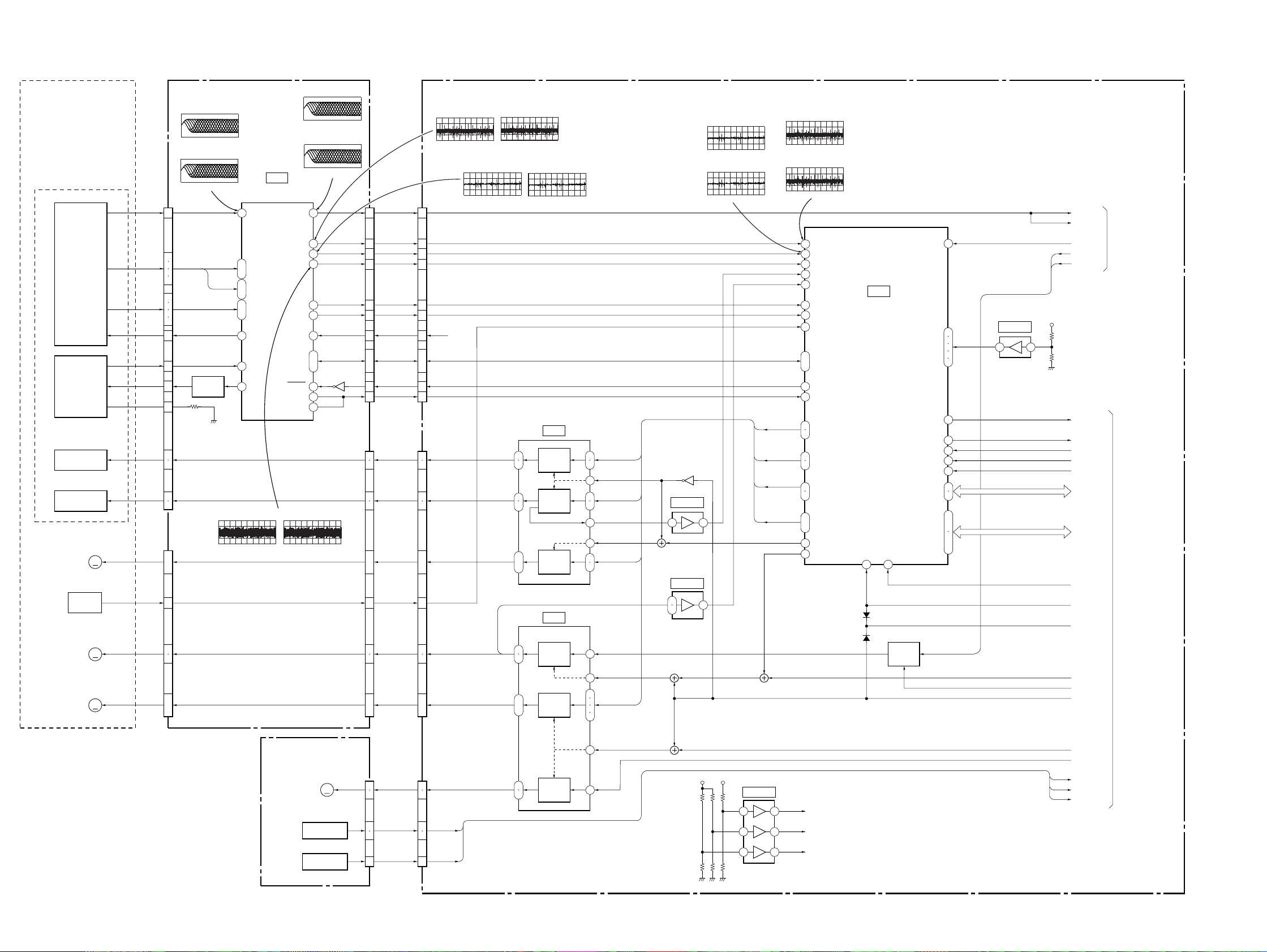
4-1. FRAME SCHEMATIC DIAGRAM
FRAME (1) SCHEMATIC DIAGRAM
FRAME (1/2)
4-3 4-4
Page 35

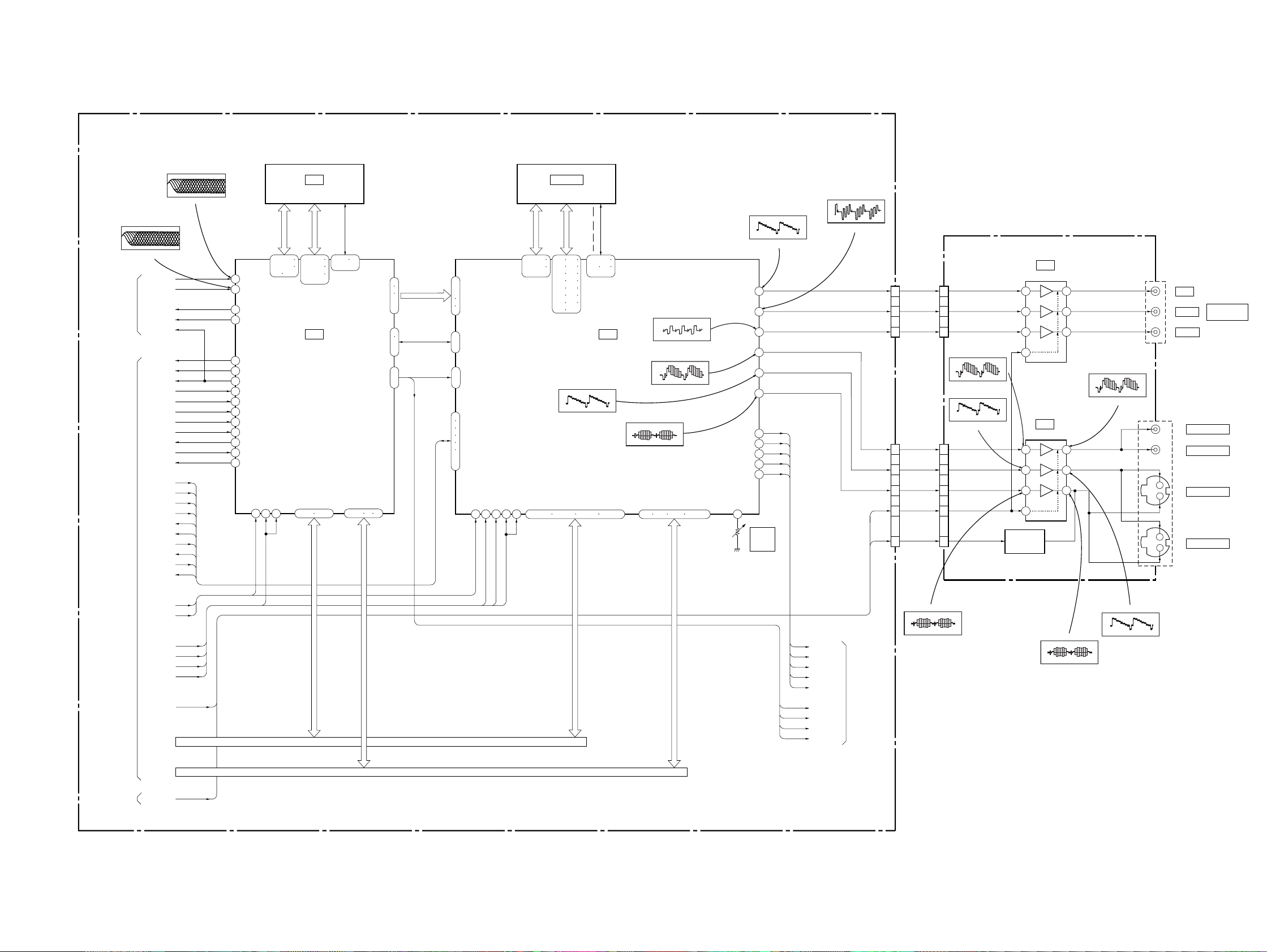
FRAME (2) SCHEMATIC DIAGRAM
DVP-S533D
4-5 4-6
FRAME (2/2)
Page 36

DVP-S533D
4-2. PRINTED WIRING BOARDS AND SCHEMATIC DIAGRAMS
There are few cases that the part isn't mounted in this model is printed on this diagram.
TK-51 (RF/SERVO) PRINTED WIRING BOARD
– Ref. No.: TK-51 board; 2,000 series –
TK-51 BOARD (SIDE A)
CN001 B-2
CN002 C-2
CN003 D-2
CN004 D-3
D003 B-2
IC001 C-1
Q001 A-2
Q002 D-1
TK-51
A
B
BOARD(SIDE A)
E
C
B
Power Block (HS-030SF)
(SWITCHING REGULATOR)
FR-150
(IR/POWER SWITCH)
HP-111
(HEADPHONE)
SW-317
(SURROUND SWITCH)
MS-46
(LOADING)
TK-51
(RF/SERVO)
FL-101
(FUNCTION SWITCH)
AU-212
(AUDIO)
MB-85
(SIGNAL PROCESS/SERVO)
C
D
E
C
B
CN003
12
1-672-677-
(12)
RF/SERVO
TK-51
05
4-7 4-8
1 2 3
Page 37

TK-51
BOARD(SIDE B)
• Wavef orms
1 IC001 1 (DVD play)
200 mV/DIV 100 ns/DIV
DVP-S533D
6 IC001 #ª (CD play)
500 mV/DIV 200 ms/DIV
536 mVp-p
2 IC001 1 (CD play)
500 mV/DIV 500 ns/DIV
880 mVp-p
3 IC001 @ª (DVD play)
200 mV/DIV 500 ms/DIV
592 mVp-p
1.7 Vp-p
7 IC001 $º (DVD play)
100 mV/DIV 50 ms/DIV
180 mVp-p
8 IC001 $º (CD play)
500 mV/DIV 50 ms/DIV
860 mVp-p
05
1-672-677-
12
(12)
4 IC001 @ª (CD play)
200 mV/DIV 20 ms/DIV
448 mVp-p
5 IC001 #ª (DVD play)
500 mV/DIV 50 ms/DIV
1.3 Vp-p
9 IC001 %¢ (DVD play)
500 mV/DIV 100 ns/DIV
1.5 Vp-p
!º IC001 %¢ (CD play)
500 mV/DIV 500 ns/DIV
1.5 Vp-p
4-9 4-10
RF/SERVO
TK-51
Page 38

DVP-S533D
TK-51 (RF/SERVO) SCHEMATIC DIAGRAM • See page 4-7 for printed wiring board and page 4-10 for waveforms.
– Ref. No.: TK-51 board; 2,000 series –
RF/SERVO
TK-51
Note:The components identified by mark ! or dotted line
with mark ! are critical for safety.
Replace only with part number specified.
4-11 4-12
Page 39

MS-46 (LOADING) PRINTED WIRING BOARD AND SCHEMATIC DIAGRAM
– Ref. No.: MS-46 board; 3,000 series –
There are few cases that the part isn't mounted in this model is printed on this diagram.
MS-46 BOARD
S001
(TRAY SENSOR)
S001
CN001
DVP-S533D
LOADING
MOTOR
(CHUCK SENSOR)
11
05
Power Block (HS-030SF)
(SWITCHING REGULATOR)
FR-150
(IR/POWER SWITCH)
TK-51
(RF/SERVO)
AU-212
(AUDIO)
1-675-146-
(11)
HP-111
(HEADPHONE)
SW-317
(SURROUND SWITCH)
MS-46
(LOADING)
MB-85
FL-101
(FUNCTION SWITCH)
(SIGNAL PROCESS/SERVO)
4-13 4-14
LOADING
MS-46
Page 40

DVP-S533D
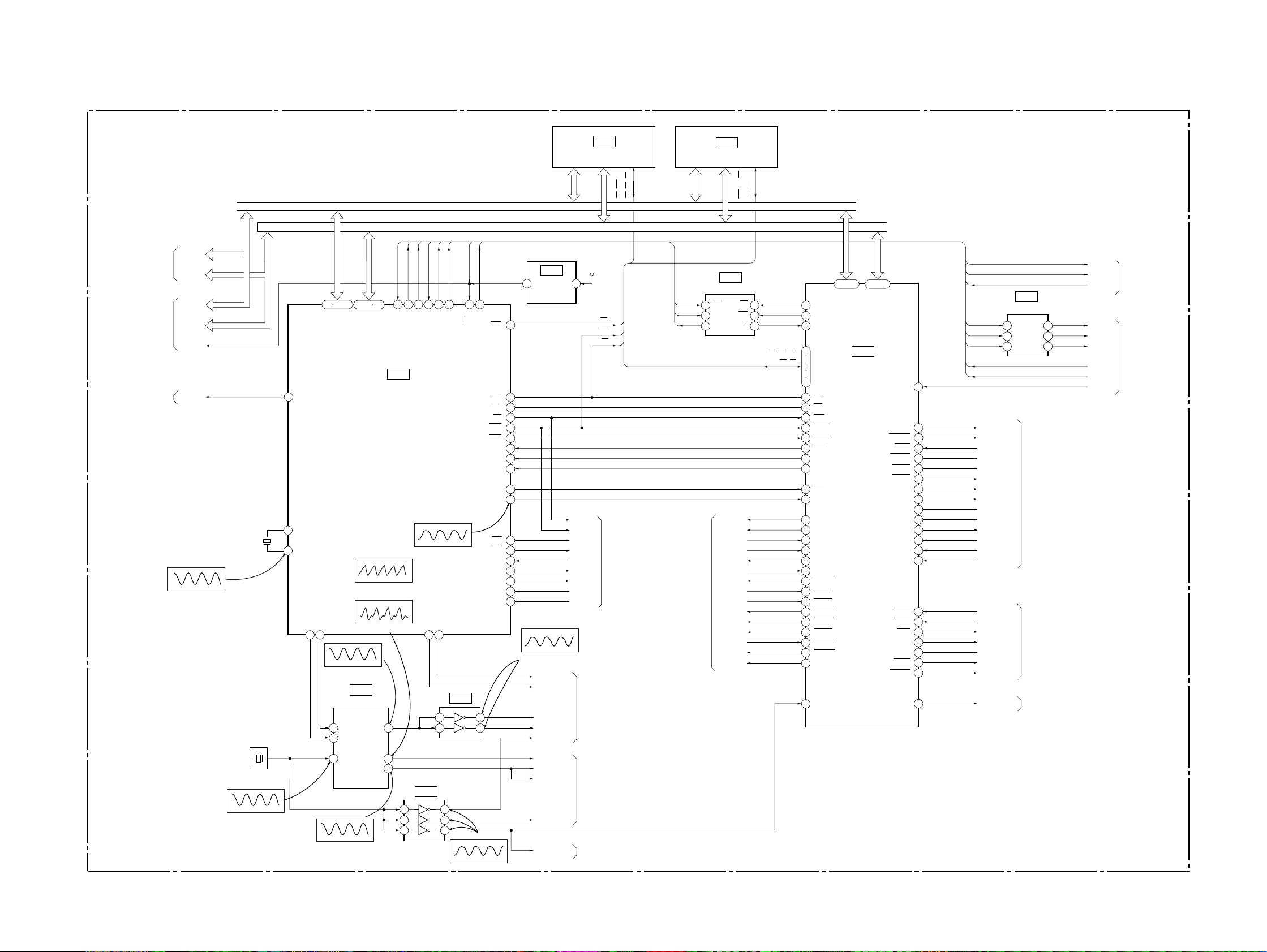
MB-85 (SIGNAL PROCESS/SERVO) PRINTED WIRING BOARD
– Ref. No.: MB-85 board; 1,000 series –
MB-85 BOARD (SIDE A)
CN001 D-2
CN002 D-4
CN003 D-5
CN004 C-1
CN005 B-1
CN006 C-7
CN007 C-1
CN010 B-6
CN011 D-6
CN012 D-6
D801 C-6
D802 C-6
D803 C-6
D804 C-6
D805 C-5
D807 C-5
IC001 A-2
IC003 A-3
IC004 B-3
IC202 A-5
IC206 B-6
IC302 D-3
IC303 C-4
IC401 C-2
IC501 A-2
IC601 A-4
IC701 C-5
IC904 A-1
Q801 C-5
Q802 C-6
Q803 C-6
There are few cases that the part isn't mounted in this model is printed on this diagram.
Power Block (HS-030SF)
(SWITCHING REGULATOR)
FR-150
(IR/POWER SWITCH)
TK-51
(RF/SERVO)
AU-212
(AUDIO)
HP-111
(HEADPHONE)
MS-46
(LOADING)
SW-317
(SURROUND SWITCH)
FL-101
MB-85
(SIGNAL PROCESS/SERVO)
(FUNCTION SWITCH)
SIGNAL PROCESS/SERVO
MB-85
4-15 4-16
Page 41

MB-85 BOARD (SIDE B)
D701 C-2
D806 C-2
IC005 A-6
IC201 A-3
IC203 A-3
IC204 B-2
IC207 A-2
IC304 C-3
IC402 C-5
IC403 C-5
IC404 D-5
IC702 B-1
IC801 C-2
IC802 C-1
IC803 C-1
IC902 A-6
IC905 B-6
IC906 B-6
IC907 C-6
DVP-S533D
4-17 4-18
SIGNAL PROCESS/SERVO
MB-85
Page 42

DVP-S533D
MB-85 (AV DECODER) SCHEMATIC DIAGRAM • See page 4-15 for printed wiring board.
– Ref. No.: MB-85 board; 1,000 series –
AV DECODER
MB-85 (1/10)
4-19 4-20
Page 43

MB-85 (SDRAM) SCHEMATIC DIAGRAM • See pag e 4-15 for printed wiring board.
– Ref. No.: MB-85 board; 1,000 series –
DVP-S533D
• Wavef orms
1 IC401 %¢
720 mVp-p (H)
2 IC401 %¶
728 mVp-p (H)
3 IC401 %•
5 IC401 ^™
816 mVp-p (H)
6 IC401 ^∞
1.2 Vp-p (H)
4 IC401 ^¡
1.0 Vp-p (H)
1.1 Vp-p (H)
SDRAM
4-224-21
MB-85 (2/10)
Page 44

DVP-S533D
1 IC701 ^ª (DVD play)
500 mV/DIV 50 ms/DIV
1.4 Vp-p
2 IC701 ^ª (CD play)
500 mV/DIV 200 mV/DIV
1.7 Vp-p
3 IC701 ^• (DVD play)
100 mV/DIV 5 ms/DIV
180 mVp-p
4IC701^• (CD play)
500 mV/DIV 50 ms/DIV
860 mVp-p
MB-85 (SERVO DSP) SCHEMATIC DIAGRAM • See page 4-15 for printed wiring board.
– Ref. No.: MB-85 board; 1,000 series –
• Wavef orms
SERVO DSP
MB-85 (3/10)
4-23 4-24
Page 45

MB-85 (DRIVE) SCHEMATIC DIAGRAM • See pag e 4-15 for printed wiring board.
– Ref. No.: MB-85 board; 1,000 series –
DVP-S533D
4-25 4-26
DRIVE
MB-85 (4/10)
Page 46

DVP-S533D
MB-85 (ARP) SCHEMATIC DIAGRAM • See page 4-15 for printed wiring board.
– Ref. No.: MB-85 board; 1,000 series –
• Wavef orms
1 IC303 !¶ (DVD play)
500 mV/DIV 100 ns/DIV
1.6 Vp-p
2 IC303 !ª (CD play)
500 mV/DIV 200 ns/DIV
1.6 Vp-p
ARP
MB-85 (5/10)
4-27 4-28
Page 47

MB-85 (SYSTEM CONTROL) SCHEMATIC DIAGRAM • See page 4-15 for printed wiring board.
– Ref. No.: MB-85 board; 1,000 series –
DVP-S533D
• Waveforms
1 IC202 (™
2.4 Vp-p (12.5 MHz)
2 IC202 5
4 Vp-p (25.3 MHz)
4-29 4-30
SYSTEM CONTROL
MB-85 (6/10)
Page 48

DVP-S533D
MB-85 (HGA) SCHEMATIC DIAGRAM • See pag e 4-15 for printed wiring board.
– Ref. No.: MB-85 board; 1,000 series –
HGA
MB-85 (7/10)
4-31 4-32
Page 49

MB-85 (CLOCK GENERATOR, AUDIO DSP) SCHEMATIC DIAGRAM • See page 4-15 for printed wiring board.
– Ref. No.: MB-85 board; 1,000 series –
DVP-S533D
• Wavef orms
1 IC004 2, 5, 7
4.2 Vp-p (26.9 MHz)
2 IC003 5, 7
DVD: 6.2 Vp-p (37.0 MHz)
CD : 5 Vp-p (33.6 MHz)
3 IC001 6
6IC001 !¢ (DVD play)
4.2 Vp-p (25.3 MHz)
7 IC001 !¢ (CD play)
4.7 Vp-p (22.5 MHz)
4.2 Vp-p (27.0 MHz)
4 IC001 !™
4.6 Vp-p (33.8 MHz)
5 IC001 !¶
DVD: 5.8 Vp-p (36.5 MHz)
CD : 5.1 Vp-p (33.8 MHz)
4-33 4-34
CLOCK GENERATOR, AUDIO DSP
MB-85 (8/10)
Page 50

DVP-S533D
MB-85 (DAC) SCHEMATIC DIAGRAM • See page 4-15 for printed wiring board.
– Ref. No.: MB-85 board; 1,000 series –
DAC
MB-85 (9/10)
4-35 4-36
Page 51

MB-85 (BIAS) SCHEMATIC DIAGRAM • See pag e 4-15 for printed wiring board.
– Ref. No.: MB-85 board; 1,000 series –
DVP-S533D
4-37 4-38
BIAS
MB-85 (10/10)
Page 52

DVP-S533D
AU-212 (AUDIO, VIDEO BUFFER) PRINTED WIRING BOARD
– Ref. No.: AU-212 board; 2,000 series –
AU-212 BOARD
CN301 B-2
CN302 B-3
CN303 B-3
CN401 C-7
D301 A-11
D304 A-5
D305 A-5
D306 A-5
D307 A-4
D308 B-2
D431 A-8
D432 A-8
D525 A-9
D526 A-8
D551 A-10
D552 A-9
D561 A-2
D591 A-11
D592 A-11
IC301 C-11
IC302 A-11
IC303 B-6
IC321 B-3
IC401 B-5
IC431 B-7
IC502 B-8
IC505 A-1
IC541 B-9
IC571 B-10
Q301 B-4
Q303 A-11
Q304 C-2
Q305 C-6
Q306 C-9
Q307 C-7
Q308 C-9
Q309 C-10
Q310 C-10
Q311 C-10
Q314 B-3
Q315 B-3
Q321 B-3
Q322 A-3
Q341 A-1
Q401 B-6
Q402 B-6
Q431 B-7
Q432 C-7
Q435 C-6
Q436 A-8
Q503 B-9
Q504 A-8
Q543 B-10
Q544 A-9
Q573 B-11
Q574 A-10
There are few cases that the part isn't mounted in this model is printed on this diagram.
Power Block (HS-030SF)
(SWITCHING REGULATOR)
FR-150
(IR/POWER SWITCH)
TK-51
(RF/SERVO)
AU-212
(AUDIO)
AUDIO, VIDEO BUFFER
AU-212
HP-111
(HEADPHONE)
MS-46
(LOADING)
SW-317
(SURROUND SWITCH)
4-39 4-40
FL-101
(FUNCTION SWITCH)
MB-85
(SIGNAL PROCESS/SERVO)
Page 53

AU-212 (AUDIO) SCHEMATIC DIAGRAM
– Ref. No.: AU-212 board; 2,000 series –
DVP-S533D
4-41 4-42
AUDIO
AU-212 (1/2)
Page 54

DVP-S533D
AU-212 (VIDEO BUFFER) SCHEMATIC DIAGRAM • See page 4-39 for printed wiring board.
– Ref. No.: AU-212 board; 2,000 series –
• Wavef orms
1 IC321 2
1.1 Vp-p (H)
2 IC321 4
1.2 Vp-p (H)
3 IC321 7
6 IC321 !∞
2.0 Vp-p (H)
860 mVp-p (H)
4 IC321 !º
5 IC321 !£
1.8 Vp-p(H)
2.4 Vp-p (H)
VIDEO BUFFER
AU-212 (2/2)
4-43 4-44
Page 55

DVP-S533D
FL-101 (FUNCTION SWITCH, IF CON) PRINTED WIRING BOARD
– Ref. No.: FL-101 board; 2,000 series –
FL-101 BOARD
CN201 C-1
CN202 C-10
CN203 C-12
D202 A-10
D203 C-1
D204 C-13
D205 B-12
D206 B-1
D207 B-1
IC201 B-9
IC202 A-10
IC203 B-12
Q201 B-1
FL-101
A
B
C
05
BOARD
PROGRAM
SHUFFLE
D203
DOLBY DIGITAL
1 2 3 4 5 6 7 8 9 10 11 12 13
FLUORESCENT INDICATOR TUBE
There are few cases that the part isn't mounted in this model is printed on this diagram.
CLEAR
REPEAT
OPEN/CLOSE
TITLE
1
3
5
4
PREV
NEXT
17
1
DVD MENU
9
1
RETURN
D204,S208
JOG
1-672-238-
12
(12)
Power Block (HS-030SF)
(SWITCHING REGULATOR)
FR-150
(IR/POWER SWITCH)
HP-111
(HEADPHONE)
SW-317
(SURROUND SWITCH)
MS-46
(LOADING)
TK-51
(RF/SERVO)
FL-101
(FUNCTION SWITCH)
AU-212
(AUDIO)
MB-85
(SIGNAL PROCESS/SERVO)
4-45 4-46
FUNCTION SWITCH, IF CON
FL-101
Page 56

DVP-S533D
FL-101 (FUNCTION SWITCH) SCHEMATIC DIAGRAM • See pages 4-45 for printed wiring board.
– Ref. No.: FL-101 board; 2,000 series –
FUNCTION SWITCH
FL-101 (1/2)
4-47 4-48
Page 57

FL-101 (IF CON) SCHEMATIC DIAGRAM • See pag es 4-45 for printed wiring board.
– Ref. No.: FL-101 board; 2,000 series –
DVP-S533D
4-49 4-50
• Waveform
1 IC201 !¢
3.9 Vp-p (4 MHz)
IF CON
FL-101 (2/2)
Page 58

DVP-S533D
05
1-672-239-
12
FR-150
BOARD
(12)
(ON/STANDBY)
3
2
1
A
B
1 2 3 4
Power Block (HS-030SF)
(SWITCHING REGULATOR)
TK-51
(RF/SERVO)
AU-212
(AUDIO)
MB-85
(SIGNAL PROCESS/SERVO)
FL-101
(FUNCTION SWITCH)
MS-46
(LOADING)
SW-317
(SURROUND SWITCH)
HP-111
(HEADPHONE)
FR-150
(IR/POWER SWITCH)
HP-111 (HEADPHONE) PRINTED WIRING BOARD AND SCHEMATIC DIAGRAM
– Ref. No.: HP-111 board; 2,000 series –
There are few cases that the part isn't mounted in this model is printed on this diagram.
HP-111
K
K
BOARD
K
K
A
A
12
1-672-241-
(12)
SW-317 (SURROUND SWITCH), FR-150 (IR/POWER SWITCH) PRINTED WIRING BOARDS
– Ref. No.: SW-317 board and FR-150 board; 4,000 series –
FR-150 BOARD
CN001 B-3
CN002 A-5
CN003 A-2
D001 A-4
D002 A-4
D003 B-4
D004 A-4
D071 A-1
IC051 A-1
Q001 A-3
Q002 A-3
05
PHONES
LEVEL
MIN MAX
SW-317
05
BOARD
1-672-240-
D098,S098
VES
12
(12)
HEADPHONE, SURROND SWITCH, IR/POWER SWITCH
HP-111, SW-317, FR-150
4-51
4-52
Page 59

SW-317 (SURROUND SWITCH), FR-150 (IR/POWER SWITCH) SCHEMATIC DIAGRAM
– Ref. No.: SW-317 board and FR-150 board; 4,000 series –
DVP-S533D
4-53 4-54
SURROUND SWITCH, IR/POWER SWITCH
SW-317, FR-150
Page 60

DVP-S533D
HS-030SF (SWITCHING REGULATOR) PRINTED WIRING BOARD
– Ref. No.: HS-030SF board; 6,000 series –
HS-030SF BOARD
CN101 A-3
CN102 C-4
CN201 A-1
CN202 B-1
CN203 B-1
D101 C-4
D102 A-3
D104 A-3
D105 A-2
D131 A-2
D132 A-2
D133 A-3
D135 A-3
D182 C-2
D183 C-2
D184 C-2
D185 C-3
D211 B-1
D212 B-2
D311 A-2
D401 C-1
D402 C-1
D511 B-2
D611 B-2
IC301 A-2
IC401 C-1
Q101 B-3
Q102 A-3
Q103 B-3
Q131 A-2
Q181 C-2
Q182 C-3
Q183 C-2
There are few cases that the part isn't mounted in this model is printed on this diagram.
Power Block (HS-030SF)
(SWITCHING REGULATOR)
FR-150
(IR/POWER SWITCH)
HP-111
(HEADPHONE)
MS-46
(LOADING)
SW-317
(SURROUND SWITCH)
SWITCHING REGULATOR
HS-030SF
TK-51
(RF/SERVO)
FL-101
(FUNCTION SWITCH)
4-55 4-56
AU-212
(AUDIO)
MB-85
(SIGNAL PROCESS/SERVO)
Page 61

HS-030SF (SWITCHING REGULATOR) SCHEMATIC DIAGRAM
– Ref. No.: HS-030SF board; 6,000 series –
12345678
DVP-S533D
A
B
C
D
HS-030SF BOARD
C112
0.047uF
C110
220uF
400V
630V
C113
47pF
2kV
R104
+
3.3M
1/2W
Q101
2SK2333
SWITCH
435
314
314
Q103
2SK2333
SWITCH
S
S
C117
0.0033uF
Q181
2SK2663
SWITCH
314
3.1
R115
314
C131
27k
10uF
50V
+
RD18FB2
S
D102
(SHORT)
C183
0.0022uF
1.2
R186
R181
27k
R152
0.22
9.0
+
D1N60
CONTROL
C186
1uF
400V
R187
180k
1/2W
R188
180k
1/2W
D184
R131
2.2k
D135
1SS270A
RD2.7ESB2
0
Q131
2SC3377
POWER
D133
448
314
R135
2.7k
R132
22k
R134
10k
Q183
2SK2663
SWITCH
C181
2200pF
S
D185
RD18
FB2
1kV
R133
1k
C132
1uF
50V
D132
1SS270A
314
R189
L182
RS204
2SC3377
1.2
SWITCH
C184
0.0047uF
D131
1SS270A
+
0.01uF
15k
0.0033uF
Q182
-0.3
C185
C182
L150
45
R182
RD2.7ESB2
R184
5.6K
3.1
Q102
2SC3377
SWITCH
330
2W
D182
-0.1
C115
0.033uF
C116
0.01uF
D104 RD3.0ESB2
50V
R113 680
R183
2.2k
R185
10K
R116
1SS270A
220
2W
R112
10K
R110 2.2K
D183
R114
2.2k
D105
1SS270A
!
PC103
TLP721F
!
PC101
TLP721F
!
!
T101
T102
D211
S2L20U
C211
330uF
35V
D311
21DQ04
D611
D3S4M
D511
S2L20U
4
AN1431T
D401
11EQS04
C401
100uF
35V
R401
B+
!
P211
500mA 60V
L311 10uH
L611 39uH
L511
10uH
R713
1k
+
R304
1.5k
R305
(SHORT)
R306
1.5k
!
C313
47uF
35V
+
P311
2.0A 60V
C512
47uF
35V
750mA 60V
!
P511
P611
!
1.5A 60V
C613
+
47uF
35V
L211
10uH
B+
C213
+
25V
47uF
C611
560uF
35V
+
35V
+
C311
+
330uF
35V
D212
RD24FB2
+
B+ B+
R301
C511
68
1000uF
B-
R303
1k
IC301
SHUNT REG
2.5
IC301
+
68
C301
+
1uF
50V
D402
RD7.5ESB1
B+
CN201 8P
1
+3.3V
2
+5V
3
B+
GND
4
+12V
5
GND
6
-12V
7
E+5V
8
GND
CN202 7P
7
+3.3V
6
+3.3V
5
+5V
4
GND
3
GND
2
M+12V
1
A+12V
CN203 6P
1
P-CONT
2
E+5V
3
+5V
4
GND
5
-12V
6
GND
AU-212 BOARD B301
(SEE PAGE 4-41)
MB-85 BOARD
CN001
(SEE PAGE 4-37)
FR-150 BOARD
CN001
(SEE PAGE 4-53)
B+
B-
R211
10
2W
B-
B+
B-
B+
E
!
CN101 2P
F101
1
1.6A
!
AC IN
05
250V
0.1µF
2
!
C101
250V
!
L101
18mH
R101
1M
1/2W
!
C103
330pF
250V
!
C102
0.1µF
250V
!
L102
18mH
!
C104
330pF
250V
!
C107
330pF
250V
D101
S1WBAO60
SHUNT REG
IC401
!
PC102
TLP721F
IC401
AN1431T
R402
C402
3.9
1uF
50V
2.5
R403
1.2k
1k
R404
+
270
R405
1.5k
Note:The components identified by mark ! or dotted line
with mark ! are critical for safety.
Replace only with part number specified.
SWITCHING REGULATOR
4-57 4-58 E
HS-030SF
Page 62

SECTION 5
Pin No. Pin name I/O Function
68 EOP0 I Not used
69 AVCC - Power supply
70 AVRH - Reference power supply (+3.3V)
71 AGND - Ground
72 AN0 I Set of mode 0
73 AN1 I Set of mode 1
74 AN2 I Set of mode 2
75 AN3 I Set of mode 3 (fixed at “H”)
76 SI0 I Serial data input from IF CON and EEPROM
77 SO0 O Serial data output to IF CON and EEPROM
78 SC0 O Serial clock output to IF CON and EEPROM
79 SI1 I Serial bus 1 (for data input)
80 SO1 O Serial bus 1 (for data output)
81 SI2 I Serial bus 2 (for data input)
82 SO2 O Serial bus 2 (for data output)
83 PF7 O Reset signal output
84 DACK1 O Output of DMA-ACK 0 to AV DEC
85 DACK0 O Output of DMA-ACK 1 to AV DEC
86 DREQ1 I Input of DMA-REQ 0 from AV DEC
87 DREQ0 I Input of DMA-REQ 1 from AV DEC
88 INT3 I Input of interrupt from HGA
89 SC1 O Serial clock output
90 GND - Ground
91 X1 O Clock output (12.5MHz)
92 X0 I Clock input (12.5MHz)
93 VCC5 - Power supply
94 INT1 I Input of interrupt ARP and SERVO DSP
95 INT0 I Input of interrupt from AV DEC
96 PB0 I Rear panel lime input select (“H”: DISC “L”: EXT)
97 PB1 O Chip select signal to IF CON
98 PB2 O Chip select signal to DAC (Lt and Rt)
99 PB3 O Chip select signal to DAC (L and R)
100 PB4 O DVD/CD select (“H”: 44.1kHz “L”: 48kHz)
5-1. SYSTEM CONTROL PIN FUNCTION (MB-85 BOARD IC202)
Pin No. Pin name I/O Function
1 PB5 O Analog filter gain control
2 PB6 O VES gain control “H”: VES
3 PB7 O Rear CH boost control “H”: rear boost
4 VCC3 - Power supply
5 CLK O CPU clock out (25 MHz)
6 CS5 O Not used
7 CS4 O Chip select signal for ARP, SERVO DSP and HGA
8 CS3 O Chip select signal for SDRAM and AV DEC
9 CS2 O Chip select signal for REG and AV DEC
10 CS1 O Chip select signal for external SRAM
11 CS0 O Chip select signal for external FLASH ROM
12 NMI I Not used (fixed at “H”)
13 HST I Not used (fixed at “H”)
14 RST I Reset signal input from IF CON
15 GND - Ground
16 MD0 I Input of mode select 0 (fixed at “1”)
17 MD1 I Input of mode select 1 (fixed at “0”)
18 MD2 I Input of mode select 2 (fixed at “0”)
19 RDY I Wait signal input
20 P81 I Test terminal (fixed at “H”)
21 P82 I Test terminal (fixed at “L”)
22 RD O Read enable signal output
23 WR0 O High byte write enable signal output (16 bit and 8 bit)
24 WR1 O Low byte write enable signal output (16 bit only)
25-32 D16-D23 I/O Data bus D0-D7 (16 bit)
33-39 D24-D30 I/O Data bus D8-D14 (16 bit), D0-D6 (8 bit)
40 GND - Ground
41 D31 I/O Data bus D15 (16 bit), D7 (8 bit)
42 A00 O Address bus A0
43 VCC5 - Power supply
44-64 A01-A21 O Address bus A1-A21
65 GND - Ground
66 P66 O PLL IC control output “H”: DOUBLE
67 P67 I DIAG mode signal input “L”: DIAG
INTERFACE, IC PIN FUNCTION DESCRIPTION
DVP-S533D
5-1
5-1 E
Page 63

SECTION 6
TEST MODE
DVP-S533D
6-1. GENERAL DESCRIPTION
The T est Mode allows you to make diagnosis and adjustment easily using the remote commander and monitor TV. The instructions,
diagnostic results, etc. are given on the on-screen display (OSD).
6-2. STARTING TEST MODE
Press [TITLE], [CLEAR], [POWER] buttons on the remote commander in this order with the power of main unit in OFF status,
and the T est Mode starts, then the menu shown below will be displayed on the TV screen. At the bottom of menu screen, the model
name and revision number are displayed.
To execute each function, select the desired menu and press its
number on the remote commander.
To exit from the Test Mode, press the POWER button.
Test Mode Menu
0. Syscon Diagnosis
1. Drive Auto Adjustment
2. Drive Manual Operation
3. Mecha Aging
4. Emergency History
5. Version Information
6. Video Level Adjustment
Exit: Power Key
_
Model : DPX12xxxx
Revision : 1.xxxx
6-3. SYSCON DIAGNOSIS
The same contents as board detail check by serial interface can be
checked from the remote commander.
On the T est Mode Menu screen, press [0] k e y on the remote commander, and the following check menu will be displayed.
### Syscon Diagnosis ###
Diag All Check
No. 2 Version
2-3. ROM Check Sum
Check Sum = xxxx
Press NEXT Key to Continue
Press PREV Key to Repeat
_
For the ROM Check, the check sum calculated by the Syscon is
output, and therefore you must compare it with the specified value
for confirmation.
Following the message, press [NEXT] key to go to the next item,
or [PREV] ke y to repeat the same check again. To quit the diagnosis and return to the Check Menu screen, press [STOP] or
[ENTER] key. If an err or occurred, the diagnosis is suspended
and the error code is displayed as shown below.
### Syscon Diagnosis ###
3-3. EEPROM Check
Error 03: EEPROM Write/Reed N
Address : 00000001
Write Data : 2492
Read Data : 2490
Press NEXT Key to Continue
Press PREV Key to Repeat
_
Press [STOP] key to quit the diagnosis, or [PREV] key to repeat
the same item where an error occurred, or [NEXT] key to continue
the check from the item next to faulty item.
### Syscon Diagnosis ###
Check Menu
0. Quit
1. All
2. Version
3. Peripheral
4. Servo
5. Supply
6. AV Decoder
7. Video
8. Audio
_
0. Quit
Quit the Syscon Diagnosis and return to the Test Mode Menu.
1. All
All items continuous check
This menu checks all diagnostic items continuously . Normally , all
items are checked successively one after another automatically
unless an error is found, but at a certain item that requires judgment through a visual check to the result, the following screen is
displayed for the key entry.
Submenu
Selecting 2 and subsequent items calls the submenu screen of each
item.
For example, if “5. Supply” is selected, the following submenu
will be displayed.
### Syscon Diagnosis ###
Check Menu
No. 5 Supply
0. Quit
1. All
2. ARP Register Check
3. ARP to RAM Data Bus
4. ARP to RAM Address Bus
5. ARP RAM Check
_
0. Quit
Quit the submenu and return to the main menu.
1. All
All submenu items continuous check
This menu checks 2 and subsequent items successively. At the
item where visual check is required for judgment or an error occurred, the checking is suspended and the message is output for
key entry. Nor mally, all items are checked successively one after
another automatically unless an error is found.
6-1
Page 64

Selecting 2 and subsequent items executes respective menus and
outputs the results.
For the contents of each submenu, see “Check Items List”.
General Description of Checking Method
2. Version
(2-2) Revision
ROM revision number is displayed.
Error: Not detected.
The revision number defined in the source file of ROM
(IC206) is displayed with four digits.
4. Servo
(4-2) Servo DSP Check
Data write → read, and accord check
Error 12: Read data discord
Data 0x9249, 0x2942, 0x4294 are written to the address
0x602 of RAM in the Servo DSP (IC701), then read and
checked.
(4-3) DSP Driver Test
Test signal data → DSP Driver
Error: Not detected.
(2-3) ROM Check Sum
Check sum is calculated.
Error: Not detected.
The 8-bit data are added at addresses 0x000F0000 ~
0x002EFFFF of ROM (IC206) and the result is displayed
with 4-digit hexadecimal number. Error is not detected.
Compare the result with the specified value.
(2-4) Model Type
Model code is displayed.
Error: Not detected.
The model code read from EEPROM (IC201) is displayed
with 2-digit hexadecimal number.
DVP-S533D (PX) 2 0
(2-5) Region
Region code is displayed.
Error: Not detected.
The region code determined from the model code is displayed.
3. Peripheral
(3-2) Gate Array Check
Data write → read, and accord check
Error 02: Gate array write/read discord
Data 0x00~0xFF are written to the address 0xF of GA
(IC601), then read and checked if they accord.
(3-3) EEPROM Check
Data write → read, and accord check
Error 03: EEPROM write/read discord
Data 0x9249, 0x2942, 0x4294 are written to addresses
0x00~0xFF of EEPROM (IC201), then read and checked.
Before writing, the data are saved, then after checking, they
are written to restore the contents of EEPROM.
Model Type
Caution: Do not conduct this test with a mechanical deck
connected.
The maximum voltage is applied to the Servo Driver IC
(IC801, IC802). If mechanical deck is connected, the motor and optics could be damaged. Disconnect mechanical
deck following the output message, then enter specified 4or 5-digit number from the remote commander, and press
the [ENTER]. The test is conducted only when the input
data accord. Check the output level, then press the [NEXT]
to finish the test.
This test is skipped if “All” is selected.
Supplement: How to disconnect mechanical deck
Disconnect flat cables connected to the CN002
and CN003 of MB-85 board. Also, disconnect
harness from the CN011.
5. Supply
Caution: Do not conduct this check with a mechanical deck con-
nected.
An access is made to the stream supply and servo control IC (IC303) and external RAM (IC304) using check
data. If mechanical deck is connected, the motor and
optics could be damaged. This check is also executed by
the “All” menu item.
Supplement: How to disconnect mechanical deck
Disconnect flat cables connected to the CN002 and
CN003 of MB-85 board. Also, disconnect harness
from the CN011.
(5-2) ARP Register Check
Data write → read, and accord check
Error 08: ARP register write, and read data discord
Data 0x00 to 0xFF are written to the TMAX register (address 0xC6) in ARP (IC303), then they are r ead and checked.
(5-3) ARP to RAM Data Bus
Data write → read, and accord check
Error 09: ARP ←→ RAM data bus error
Data 0x0001 to 0x8000 where one bit each is set to 1 are
written to the address 0 of RAM (IC304) connected to the
ARP (IC303) through the bus, then they are read and
checked. In case of discord, written bit pattern and read
data are displayed. If data where multiple bits are 1 are
read, the bits concerned may touch each other. Further, if
data where certain bit is always 1 or 0 regardless of written
data, the line could be disconnected or shorted.
6-2
Page 65

(5-4) ARP to RAM Address Bus
Data write → other address read discord check
Error 10: ARP → RAM address bus error
Caution: Address and data display in case of an error is
different from the display of other diagnosis (de-
scribed later).
Before starting the test, all addresses of RAM (IC304) are
cleared to 0x0000.
First, 0xA55A is written to the address 0x00000, and the
address data are read and checked from addresses 0x00001
to 0x80000 while shifting 1 bit each. Next, the data at that
address is cleared, and it is written to the address 0x00001,
and read and checked in the same manner. This check is
repeated up to the address 0x80000 while shifting the address data by 1 bit each.
If data other than 0 is read at the addresses except written
address, an error is given because all addresses were already cleared to 0. In this check, the error display pattern is
different from that of other diagnosis; read data, written
address, and read address are displayed in this order. Ho wever , the message uses same template, and accordingly e xchange Address and Data when reading. The following display, for example,
### Syscon Diagnosis ###
5-4. ARP to RAM Address Bus
Error 10: ARP - RAM Address B
Address : 0000A55A
Write Data : 00000000
Read Data : 00080000
Press NEXT Key to Continue
Press PREV Key to Repeat
_
6. AV Decoder
(6-2) 1930 RAM
Data write → read, and accord check
Error 13: AVD RAM read data discord
The program code data stored in ROM (IC206) are copied
to all areas of RAM (IC402, IC403) connected to the AVD
(IC401) through the bus, then they are read and checked if
they accord. Further, the same test is conducted once again
with the data where all bits are inverted between 1 and 0. If
discord is detected, faulty address, written data, and read
data are displayed following the error code 13, and the test
is suspended.
(6-3) 1930 SP
ROM → AVD RAM → Video OUT
Error: Not detected.
The data including sub picture streams in ROM (IC206)
are transferred to the RAM (IC402, IC403) in AVD (IC401),
and output as video signals from the AVD (IC401).
They are output from all video terminals (Composite, Y/C,
Component) except EURO AV terminal.
7. Video
(7-2) Color Bar
AVD color bar command write → Video OUT
Error: Not detected.
The command is transferred to the AVD, and the color bar
signals are output from video terminals.
They are output from all video terminals (Composite, Y/C,
Component) except EURO AV terminal.
8. Audio
(8-2) ARP → 1930
Error 14: ARP → 1930 video NG
15: ARP → 1930 audio NG
shows the data 0xA55A was read from address 0x00080000
though it was written to the address 0x00000000. This implies that these addresses are in the form of shadow. Also,
if the read data is not 0xA55A, another error will be present.
(5-5) ARP RAM Check
Data write → read, and accord check
Error 11: ARP RAM read data discord
The program code data stored in ROM are copied to all
areas of RAM (IC304) connected to the ARP (IC303)
through the bus, then they are read and checked if they accord. If the detail check was selected initially, the data are
written to all areas and read, then the same test is conducted
once again with the data where all bits are inverted between
1 and 0. If discord is detected, faulty address, written data,
and read data are displayed following the error code 11,
and the test is suspended.
(8-3) Test Tone
A pink noise signal is output from the AVD (IC401) through
optical coaxial digital terminal and analog audio terminal.
Error: Not detected.
All channels → 2ch Left → 2ch Right → Front Left →
Front Right → Rear Left → Rear Right → Center → Sub
Woofer are checked in this order.
Caution: Sub Woofer is checked only for low-frequency
components, and no sound will be heard unless a
proper super woofer is connected.
6-3
Page 66

Check Items List
2) Version
(2-2) Revision
(2-3) ROM Check Sum
(2-4) Model Type
(2-5) Region
3) Peripheral
(3-2) Gate Array Check
(3-3) EEPROM Check
4) Servo
(4-2) Servo DSP Check
(4-3) DSP Driver Test
5) Supply
(5-2) ARP Register Check
(5-3) ARP to RAM Data Bus
(5-4) ARP to RAM Address Bus
(5-5) ARP RAM Check
6) AV Decoder
(6-2) 1930 RAM
(6-3) 1930 SP
7) Video
(7-2) Color Bar
Error Codes List
00: Error not detected
01: RAM write/read data discord
02: Gate array NG
03: EEPROM NG
08: ARP register read data discord
09: ARP ←→ RAM data bus error
10: ARP ←→ RAM address bus error
11: ARP RAM read data discord
12: Servo DSP NG
13: 1930 SDRAM NG
14: ARP → 1930 video NG
15: ARP → 1930 audio NG
16: 1910 UCODE download NG
17: System call error (function not supported)
18: System call error (parameter error)
19: System call error (illegal ID number)
20: System call error (time out)
90: Error occurred
91: User verification NG
92: Diagnosis cancelled
8) Audio
(8-2) ARP → 1930
(8-3) Test Tone
6-4
Page 67

6-4. DRIVE AUTO ADJUSTMENT
On the T est Mode Menu screen, press [1] k e y on the remote commander, and the drive auto adjustment menu will be displayed.
1. DVD-SL (single layer)
Select [1], insert DVD single layer disc, and press [ENTER] key,
and the adjustment will be made through the following steps, then
adjusted values will be written to the EEPROM.
## Drive Auto Adjustment ##
Adjustment Menu
0. ALL
1. DVD-SL
2. CD
3. DVD-DL
4. SACD
Exit: RETURN
Normally, [0] is selected to adjust DVD (single layer), CD, DVD
(dual layer), and SACD in this order. But, individual items can be
adjusted for the case where adjustment is suspended due to an
error. In this mode, the adjustment can be made easily through the
operation following the message displayed on the screen.
The disc used for adjustment must be the one specified for adjustment. However, for SACD disc, use the player with initial data if
the disc is not available.
0. ALL
Select [0] and press [ENTER] key, and the servo set data in
EEPROM will be initialized. Then, 1. DVD-SL disc, 2. CD disc,
3. DVD-DL disc, and 4. SACD disc are adjusted in this order.
Each time one disc was adjusted, it is ejected. Replace it with the
specified disc following the message. Though the message to confirm whether discs other than SACD disc are adjusted is not displayed, you can finish the adjustment if pressing the
ton. During adjustment of each disc, the measurement for disc
type judgment is made. As automatic adjustment does not judge
the disc type unlike conventional models, take care not to insert
wrong type discs. Also, do not give a shock during adjustment.
[STOP] but-
DVD Single Layer Disc Adjustment Steps
1. SLED TIL T Reset
2. Disc Check Memory SL
3. Wait 300 msec
4. Set Disc Type SL
5. LD ON
6. Spdl Start
7. Wait 1 sec
8. Focus Servo ON 0
9. Auto Track Offset Adjust
10. CLVA ON
11. Wait 500 msec
12. Tracking ON
13. Wait 1 sec
14. Sled ON
15. Check CLV Lock
16. Auto LFO Adjust
17. Auto Focus Offset Adjust
18. Auto Tilt Position Adjust
19. Auto Focus Gain Adjust
20. Auto Focus Offset Adjust
21. EQ Boost Adjust
22. Auto LFO Adjust
23. Auto Track Gain Adjust
Search Check
24. 32Tj Fwd
25. 32Tj Rev
26. 500Tj Fwd
27. 500Tj Rev
28. All Servo Stop
29. Eep Copy Loop Filter Offset
6-5
Page 68

2. CD
Select [2], insert CD disc, and press [ENTER] key, and the adjustment will be made through the following steps, then adjusted values will be written to the EEPROM.
3. DVD-DL (dual layer)
Select [3], insert DVD dual layer disc, and press [ENTER] key,
and the adjustment will be made through the following steps, then
adjusted values will be written to the EEPROM.
CD Adjustment Steps
1. Sled Tilt Rest
2. Disc Check Memory CD
3. Wait 500 msec
4. Set Disc Type CD
5. LD ON
6. Spdl Start
7. Wait 500 msec
8. Focus Servo ON 0
9. Auto Track Offset Adjust
10. CLVA ON
11. Wait 500 msec
12. Tracking ON
13. (TC Display Start)
14. Wait 1 sec
15. Jitter Display Start
16. Sled ON
17. Check CLV ON
18. Auto LFO Adjust
19. Auto Focus Offset Adjust
20.
21. Auto Focus Gain Adjust
22. Auto Focus Offset Adjust
23. Eq Boost Adjust
24. Auto LFO Adjust
25. Auto Track Gain Adjust
Search Check
26. 32Tj Fwd
27. 32Tj Rev
28. 500Tj Fwd
29. 500Tj Rev
30. All Servo Stop
DVD Dual Layer Disc Adjustment Steps
1. Sled Tilt Reset
2. Disc Check Memory DL
3. Wait 500 msec
4. Set Disc Type DL
5. LD ON
6. Spdl Start
7. Wait 1 sec
Layer 1 Adjust
8. Focus Servo ON 0
9. Auto Track Offset Adjust
10. Clva ON
11. Wait 500 msec
12. Tracking ON
13. Wait 500 msec
14. Sled ON
15. Check CLV Lock
16. Auto Loop Filter Offset Auto Focus Adjust
17.
18. Auto Focus Gain Adjust
19. Auto Focus Offset Adjust
20. Eq Boost Adjust
21. Auto Loop Filter Offset
22. Auto Track Gain Adjust
Search Check
23. 32Tj Fwd
24. 32Tj Rev
25. 500Tj Fwd
26. 500Tj Rev
Layer 0 Adjust
27. Fj (L1 -> L0)
28. Auto Track Offset Adjust L0
29. Clva ON
30. Wait 500 msec
31. Tracking ON
32. Wait 500 msec
33. Sled ON
34. Check CLV Lock
35. Auto Focus Filter Offset
36. Auto Focus Adjust
37.
38. Auto Focus Gain Adjust
39. Auto Focus Offset Adjust
40. Eq Boost Adjust
41. Auto Loop Filter Offset
42. Auto Track Gain Adjust
Search Check
43. 32Tj Fwd
44. 32Tj Rev
45. 500Tj fwd
46. 500Tj Rev
Layer Jump Check
47. Lj (L0 -> L1)
48. Lj (L1 -> L0)
49. All Servo Stop
6-6
Page 69

4. SACD
Select [4], insert SACD disc, and press [ENTER] key, and the
adjustment will be made through the following steps, then adjusted
values will be written to the EEPROM. However, if SACD disc is
not available, use the player with initial data, skipping the SACD
adjustment. In this case, you can finish the adjustment if pressing
the [STOP] button.
6-5. DRIVE MANUAL OPERATION
On the T est Mode Menu screen, select [2], and the manual operation menu will be displayed. For the manual operation, each servo
on/off control and adjustment can be executed manually.
## Drive Manual Operation ##
SACD Adjustment Steps
1. Sled Tilt Reset
2. Set Disc Type CD
3. LD ON
4. Spdl Start
5. Wait 500 msec
6. Focus Servo ON 0
7. Auto track Offset Adjust
8.
9. CL VA ON
10. Wait 500 msec
11. Tracking ON
12. Wait 1 sec
13. Sled ON
14. Check CLV ON
15. Auto Focus Offset Adjust
17.
18. Auto Focus Gain Adjust
19. Auto Focus Offset Adjust
20. Eq Boost Adjust
21. Auto LFO Adjust
22. Auto Track Gain Adjust
23. 32Tj Fwd
24. 32Tj Rev
25. 500Tj Fwd
26. 500Tj Rev
27. All Servo Stop
1. Disc type
Operation Menu
2. Servo Control
3. Track/Layer Jump
4. Manual Adjustment
5. Auto Adjustment
6. Memory Check
0. Disc Check Memory
Exit: Return
In using the manual operation menu, take care of the following
points. These commands do not provide protection, thus requiring
correct operation. The sector address or time code field is displayed when a disc is loaded.
1. Set correctly the disc type to be used on the Disc Type
screen.
The disc type must be set after a disc was loaded.
The set disc type is cleared when the tray is opened.
2. After power ON, if the Drive Manual Operation was selected, first perform “Reset SLED TILT” by opening 1.
Disc Type screen.
3. In case of an alarm, immediately press the [STOP] button to stop the servo operation, and turn the power OFF.
Basic operation (controllable from front panel or remote commander)
[POWER] Power OFF
[STOP] Servo stop
[OPEN/CLOSE] Stop+Eject/Loading
[RETURN] Return to Operation Menu or Test Mode
Menu
[NEXT], [PREV] Transition between sub modes of menu
[1] to [9], [0] Selection of menu items
Cursor UP/DOWN Increase/Decrease in manually adjusted
value
6-7
Page 70

0. Disc Check Memory
Disc Check
1. SL Disc Check
2. CD Disc Check
3. DL Disc Check
0. Reset SLED TILT
1. Disc Type Auto Check
Disc Type
2. DVD SL 12 cm
3. DVD DL 12 cm
4. CD 12cm
5. SACD 12 cm
6. DVD SL 8 cm
7. DVD DL 8 cm
8. CD 8 cm
9. SACD 8 cm
0. Reset SLED TILT
TC. : : EMG. 00
CD 12 cm
Display when CD 12cm disc was selected
On this screen, the mirror time is measured to judge the disc and it
is written to the EEPROM. First load DVD SL disc and press [1],
next load CD disc and press [2], and finally load DVD DL disc
and press [3].
The adjustment must be executed more than once after default
data were written. External vibration or shock to the player must
not be given. Reference value for DVD is from 10 to 20, and for
CD, from 28 to 4F.
Check that the value of CD is larger than that of DVD.
When those values are beyond a range perform this adjustment
again.
From this screen, you can go to another mode by pressing [NEXT]
or [PREV] key , but you cannot enter this mode from another mode.
You can enter this mode from the Operation Menu screen only.
1. Disc T ype
Disc Type
1. Disc Type Auto Check
2. DVD SL 12 cm
3. DVD DL 12 cm
4. CD 12cm
5. SACD 12 cm
6. DVD SL 8 cm
7. DVD DL 8 cm
8. CD 8 cm
9. SACD 8 cm
0. Reset SLED TILT
EMG. 00
[0] Reset SLED TILT Reset the Sled and Tilt to initial posi-
tion.
[1] Disk Type Check Judge automatically the loaded disc. As
the judged result is displayed at the bottom of screen, make sure that it is correct.
If Disc Check Memory menu has not
been executed after EEPROM default
setting, the disc type cannot be judged.
In this case, return to the initial menu
and make a check for three types of
discs (SL, DL, CD).
[2] to [9] Select the loaded disc. The adjusted
value is written to the address of selected disc. No further entry is necessary if [1] was selected.
2. Servo Control
Servo Control
1. LD Off R.Sled FWD
2. SP Off L.Sled REV
3. Focus Off
4. TRK. Off
5. Sled Off
6. CLVA Off
7. FCS. Srch Off
On this screen, select the disc type. To select the disc type, press
the number of the loaded disc. The selected disc type is displayed
at the bottom. Selecting [1] automatically selects and displays the
disc type. In case of wrong display, retry “Disc Check Memory”.
Also, opening the tray causes the set disc type to be cleared. In
this case, set the disc type again after loading.
In performing manual operation, the disc type must be set.
Once the disc type has been selected, the sector address or time
code display field will appear as shown below. T hese values are
displayed when PLL is locked.
Disc Type
1. Disc Type Auto Check
2. DVD SL 12 cm
3. DVD DL 12 cm
4. CD 12cm
5. SACD 12 cm
6. DVD SL 8 cm
7. DVD DL 8 cm
8. CD 8 cm
9. SACD 8 cm
0. Reset SLED TILT
SA. SI. EMG. 00
DVD SL 12 cm
Display when DVD SL 12cm disc was selected
0. Reset SLED TILT
SA. SI. EMG. 00
DVD SL 12 cm
On this screen, the servo on/off control necessary for replay is
executed. Normally, turn on each servo from 1 sequentially and
when CLV A is turned on, the usual trace mode becomes acti ve . In
the trace mode, DVD sector address or CD time code is displayed.
This is not displayed where the spindle is not locked.
The spindle could run overriding the control if the spindle system
is faulty or RF is not present. In such a case, do not operate CLV A.
6-8
Page 71

[0] Reset SLED TILT Reset the Sled and Tilt to initial posi-
tion.
[1] LD Turn ON/OFF the laser.
[2] SP Turn ON/OFF the spindle.
6-6. MECHA AGING
### Mecha Aging ###
[3] Focus Search the focus and turn on the focus.
[4] TRK Turn ON/OFF the tracking servo.
[5] Sled Turn ON/OFF the sled servo.
[6] CLVA Turn ON/OFF normal servo of spindle
servo.
[7] FCS. Srch Apply same voltage as that of focus
search to the focus drive to check the
focus drive system.
→ Sled FWD Move the sled outward. Perform this
operation with the tracking servo turned
off.
← Sled REV Move the sled inward. Perform this op-
eration with the tracking servo turned
off.
↑ Tilt UP Move the tilt upward.
↓ Tilt DOWN Move the tilt downward.
The following menus are normally not used.
3. Track/Layer Jump
Press OPEN key
Abort: STOP key
On the Test Mode Menu screen, selecting [3] executes the aging
of mechanism. First, open the tray and load a disc. Press the [PLAY]
key , and the aging will start. When the tray is closed, the disc type
and size are judged and displayed. During aging, the repeat cycle
is displayed. Aging can be aborted at any time by pressing the
[STOP] key. After the operation has stopped, unload the disc and
press again the [STOP] key or the [RETURN] ke y to return to the
Test Mode Menu.
6-7. EMERGENCY HISTORY
### MEG. History ###
Laser Hours CD xxxxxxxh
DVD xxxxxxxh
1. 00 00 00 00 00 00 00 00
00 00 00 00 00 00 00 00
2. 00 00 00 00 00 00 00 00
00 00 00 00 00 00 00 00
4. Manual Adjustment
5. Auto Adjustment
The persons who do not know well about these menus should not
use them.
6. Memory Check
EEPROM DATA
CD – DVD –
ID No. 00 SACD SL L0 L1
Focus Gain xx xx xx xx xx
TRK. Gain xx xx xx xx xx
Focus Offset xx xx xx xx xx
TRK. Offset xx xx xx xx xx
L. F. Offset xx xx xx xx xx
EQ Boost xx xx xx xx xx
Jitter xx xx xx xx xx
Mirror Time xx xx xx xx xx
_
CLEAR: Default Set
This screen displays current servo adjusted data stored in the
EEPROM. Though adjusted data can be initialized with the
[CLEAR] key, they cannot be restored after initialization.
So, before clearing, make a note of the adjusted data.
For reference, the drive has been designed so that the gain center
value is 20 and offset value is 80. Other values will be in a range
of 10 to 80. If extreme value such as 00 or FF is set, adjustment
will be faulty. In such a case, check for disc scratch or cable disconnection, then perform adjustment again.
Select: 1 – 9 Scroll: UP/DOWN
(1: Last EMG.) Exit: Return
On the Test Mode Menu screen, selecting [4] displays the information such as servo emergency history. The history information
from last 1 up to 10 can be scrolled with ↑key or↓key . Also,
specific information can be displayed by directly entering that
number with ten keys.
The upper two lines display the laser ON total hours. Data below
minutes are omitted.
Clearing History Information
Clearing laser hours
Press [DISPLAY] and [CLEAR] keys in this order.
Both CD and DVD data are cleared.
Clearing emergency history
Press [TITLE] and [CLEAR] keys in this order.
Initializing set up data
Press [DVD] and [CLEAR] keys in this order.
The data have been initialized when “Set Up Initialized” message is displayed. The EMG. History screen will be restored
soon.
6-9
Page 72

How to see Emergency History
6-8. VERSION INFORMATION
31.12
2
1 : Emergency Code
2 : Don’t Care
These codes are used for verification of software designing.
3 : Historical order 1 to 9
Emergency Codes List
10: Communication to IC001 (TK-51 board) failed.
11: Each servo for focus, tracking, and spindle is unlocked.
12: Communication to EEPROM, IC201 (MB-85 board) failed.
13: Writing of hours meter data to EEPROM, IC201 (MB-85
board) failed.
14: Communication to Servo DSP IC701 (MB-85 board) failed,
or Servo DSP is faulty.
20: Initialization of tilt servo and sled servo failed. They are not
placed in the initial position.
21: Tilt servo operation error
22: Syscon made a request to move the tilt servo to wrong posi-
tion.
23: Sled servo operation error
24: Syscon made a request to move the sled servo to wrong posi-
tion.
30: Tracking balance adjustment error
31: Tracking gain adjustment error
32: Focus balance adjustment error
33: Focus bias adjustment error
34: Focus gain adjustment error
35: Tilt servo adjustment error
36: RF equalizer adjustment error
37: RF group delay adjustment error
38: Jitter value after adaptive servo operation is too large.
40: Focus servo does not operate.
41: With a dual layer (DL) disc, focus jump failed.50: CLV
(spindle) servo does not operate.
51: Spindle does not stop.
60: With a DVD disc, Syscon made a request to seek nonexistent
address.
61: With a CD disc, Syscon made a request to seek nonexistent
address.
62: With a CD disc, Syscon made a request to seek nonexistent
track No. and index No.
63: With a DVD disc, seeking of target address failed.
64: With a CD disc, seeking of target address failed.
65: With a CD disc, seeking of target index failed.
70: With a DVD disc, physical information data could not be read.
71: With a CD disc, TOC data could not be read.
80: Disc type judgment failed.
81: As disc type judgment failed, retry was repeated.
82: As disc type judgment failed, a measurement error occurred.
83: Disc type could not be judged within the specified time.
84: Illegal command code was received from Syscon.
85: Illegal command was received from Syscon.
## Version Information ##
IF con. Ver. x. xxx (xxxx)
Group 00
SYScon. Ver. x. xxx (xxxx)
Model xx
Region 0x
SW1 ??
SW2 ??
Exit: RETURN
On the Test Mode Menu screen, selecting [5] displays the ROM
version and region code.
The parenthesized hexadecimal number in version field is
checksum value of ROM.
6-9. VIDEO LEVEL ADJUSTMENT
On the Test Mode Men u screen, selecting [6] displays color bars
for video level adjustment. During display of color bars, OSD disappears but the menu screen will be restored if pressing any key.
Measurement point : LINE OUT VIDEO
(75 Ω terminating resistance)
Measuring instrument: Oscilloscope
Adjustment device : RV401 on MB-85 board
Specified value : 1.0 ± 0.02 Vpp
1.0 ± 0.02 Vp-p
6-10
6-10 E
Page 73

SECTION 7
ELECTRICAL ADJUSTMENTS
DVP-S533D
In making adjustment, refer to 7-3. Adjustment
Related Parts Arrangement.
Note: During diagnostic check, the characters and color bars can
be seen only with the NTSC monitor. Therefore, for diagnostic check, use the monitor that supports both NTSC and
P AL modes
This section describes procedures and instructions necessary for
adjusting electrical circuits in this set.
Instruments required:
1) Color monitor TV
2) Oscilloscope 1 or 2 phenomena, band width over 100 MHz,
with delay mode
3) Frequency counter (over 8 digits)
4) Digital voltmeter
5) Standard commander
(RMT-D108A)
6) DVD reference disc
HLX-501 (J-6090-071-A) (dual layer)
HLX-503 (J-6090-069-A) (single layer)
HLX-504 (J-6090-088-A) (single layer)
HLX-505 (J-6090-089-A) (dual layer)
7) SACD reference disc
HLXA-509 (J-6090-090-A)
7-1. POWER SUPPLY ADJUSTMENT
1. Power Supply Check (HS-030SF BOARD)
Mode E-E
Instrument Digital voltmeter
+5 V Check
Test point CN202 pin 5
Specification 5.0 ± 0.2 Vdc
+3.3 V Check
Test point CN202 pin 7
Specification 3.3 ± 0.2 Vdc
EVER+5 V Check
Test point CN203 pin 2
Specification 5.0 ± 0.2 Vdc
P_CONT Check
Test point CN203 pin 1
Specification 4V – 5 Vdc
A +12 V Check
Test point CN202 pin 1
Specification 9.5 Vdc
–12 V Check
Test point CN203 pin 5
Specification –12.0 ± 1.0 Vdc
M +12 V Check
Test point CN202 pin 2
Specification 12.0 ± 1.0 Vdc
+1.5
–0.5
Checking method:
1) Confirm that each voltage satisfies the specification.
7-1
Page 74

7-2. ADJUSTMENT OF VIDEO SYSTEM
1. Video Level Adjustment (MB-85 BOARD)
<Purpose>
This adjustment is made to satisfy the NTSC standard, and if not
adjusted correctly, the brightness will be too large or small.
3. Checking Component Video Output B-Y
(MB-85 BOARD)
<Purpose>
This checks component video output B-Y. If it is incorrect, correct colors will not be displayed when connected to, for instance,
projector.
Mode Video level adjustment in test mode
Signal Color bars
Test point
LINE OUT (VIDEO) connector
(75 Ω terminated)
Instrument Oscilloscope
Adjusting element RV401
Specification 1.0 ± 0.02 Vp-p
Adjusting method:
1) In the test mode initial menu “6” Video Level Adjustment, set
so that color bars are generated.
2) Adjust the RV401 to a ttain 1.0 ± 0.02 Vp-p.
1.0 ± 0.02 Vp-p
Figure 7-1
2. S-terminal Output Check (MB-85 BOARD)
<Purpose>
Check S-terminal video output. If it is incorrect, pictures will not
be displayed correctly in spite of connection to the TV with a Sterminal cable.
Mode Video level adjustment in test mode
Signal Color bars
Test point
S VIDEO OUT (S-Y) connector
(75 Ω terminated)
Instrument Oscilloscope
Specification 1.0 ± 0.1 Vp-p
Checking method:
1) In the test mode initial menu “6” Video Level Adjustment, set
so that color bars are generated.
2) Confirm that the S-Y level is 1.0 ± 0.1 Vp-p.
Mode Video level adjustment in test mode
Signal Color bars
Test point
COMPONENT VIDEO OUT (B-Y)
connector (75 Ω terminated)
Instrument Oscilloscope
Specification 700 ± 70 mVp-p
Checking method:
1) Confirm that the B-Y level is 700 ± 70 mVp-p.
700 ± 70 mVp-p
Figure 7-3
4. Checking Component Video Output R-Y
(MB-85 BOARD)
<Purpose>
This checks component video output R-Y. If it is incorrect, correct colors will not be displayed when connected to, for instance,
projector.
Mode Video level adjustment in test mode
Signal Color bars
Test point
COMPONENT VIDEO OUT (R-Y)
connector (75 Ω terminated)
Instrument Oscilloscope
Specification 700 ± 70 mVp-p
Checking method:
1) Confirm that the R-Y level is 700 ± 70 mVp-p.
Figure 7-2
700 ± 70 mVp-p
1.0 ± 0.1 Vp-p
Figure 7-4
7-2
Page 75

5. Checking Component Video Output Y
12
2728
CN005
RV401
VIDEO LEVEL ADJ
1
1
7
6
CN202
CN203
(MB-85 BOARD)
<Purpose>
This checks component video output Y. If it is incorrect, correct
brightness will not be attained when connected to, for instance,
projector.
Mode Video level adjustment in test mode
Signal Color bars
Test point
COMPONENT VIDEO OUT (Y)
connector (75 Ω terminated)
Instrument Oscilloscope
Specification 1.0 ± 0.1 Vp-p
Checking method:
1) Confirm that the Y level is 1.0 ± 0.1 Vp-p.
1.0 ± 0.1 Vp-p
Figure 7-5
7-3. ADJUSTMENT RELATED PARTS ARRANGEMENT
MB-85 BOARD (SIDE A)
6. Checking S Video Output S-C (MB-85 BOARD)
<Purpose>
This checks whether the S-C satisfies the NTSC Standard. If it is
not correct, the colors will be too dark or light.
Mode Video level adjustment in test mode
HS-030SF BOARD (SIDE A)
Signal Color bars
Test point CN005 pin 5
Instrument Oscilloscope
Specification 286 ± 50 mVp-p
Connection:
5
4
CN005
Oscilloscope
100µF
+
75Ω
±1%
100k
±1%
Checking method:
1) Confirm that the S-C burst is 286 ± 50 mVp-p.
286 ± 50 mVp-p
Figure 7-6
7-3 7-4 E
Page 76

8-1. EXPLODED VIEWS
NOTE:
• -XX and -X mean standardized parts, so they may
have some difference from the original one.
• Items marked “*” are not stocked since they are
seldom required for routine service. Some delay
should be anticipated when ordering these items.
8-1-1. CASE ASSEMBLY
SECTION 8
REPAIR PARTS LIST
• The mechanical parts with no reference number in
the exploded views are not supplied.
• Accessories and packing materials are given in the
last of the electrical parts list.
5
DVP-S533D
The components identified by mark
! or dotted line with mark ! are critical for safety.
Replace only with part number specified.
7
4
4
8
4
3
3
2
1
1 3-975-726-71 EMBLEM, DVD
2 3-053-498-31 COVER (BK), TRAY
3 3-970-608-01 SUMITITE (B3), +BV
4 3-710-901-41 SCREW, TAPPING
6
Front panel section
Ref. No. Part No. Description RemarkRef. No. Part No. Description Remark
5 3-055-503-01 CASE (M), TOP
6 3-973-973-01 FOOT (S)
7 1-418-320-21 COMMANDER, STANDARD (RMT-D108A)
8 3-053-633-01 COVER, BATTERY (for RMT-D108A)
8-1
Page 77

8-1-2. FRONT PANEL ASSEMBLY
116
121
not supplied
124
not
supplied
116
116
not
supplied
104
103
110
101
119
112
111
120
105
106
102
122
107
108
110
109
123
113
116
115
114
117
116
118
116
116
not
supplied
101 X-3949-908-1 PANEL ASSY, FRONT
102 3-054-221-01 WINDOW (FL)
103 3-974-997-31 WINDOW, REMOTE CONTROL
104 4-963-404-21 EMBLEM (5-A), SONY
105 3-053-954-01 BUTTON, POWER
106 X-3949-836-1 BUTTON (VES) ASSY
107 3-054-219-21 BUTTON (PROG)
108 3-054-651-01 BUTTON (OPEN)
109 3-054-220-01 BUTTON (PLAY)
110 3-053-504-11 CUSHION
111 3-053-955-01 INDICATOR, POWER
112 X-3949-779-1 RING ASSY, SHUTTLE
Ref. No. Part No. Description RemarkRef. No. Part No. Description Remark
113 3-054-218-01 BUTTON, JOG
114 3-054-224-31 STICK, CURSOR
115 1-418-097-11 ENCODER, ROTARY
116 4-951-620-01 SCREW (2.6X8), +BVTP
117 1-790-167-11 CABLE, FLEXIBLE FLAT (FMF-35)
* 118 A-6065-316-A FL-101 BOARD, COMPLETE
119 3-054-217-31 KNOB, VOLUME
120 2-118-268-01 NUT (M9), HEXAGON
* 121 3-684-436-01 PLATE, MOUNT
* 122 A-6065-315-A HP-111 BOARD, COMPLETE
* 123 A-6065-317-A SW-317 BOARD, COMPLETE
* 124 A-6065-314-A FR-150 BOARD, COMPLETE
8-2
Page 78

8-1-3. CHASSIS ASSEMBLY
152
not
supplied
not
supplied
152
not
supplied
Mechanism deck
159
not
supplied
163
161
152
158
163
162
160
not
supplied
163
156
163
163
163
155
154
not
supplied
not
supplied
not
supplied
166
B
167
* 151 A-6065-318-A MB-85 BOARD, COMPLETE
152 3-970-608-01 SUMITITE (B3), +BV
153 1-790-166-11 CABLE, FLEXIBLE FLAT (FMT-25)
154 1-790-163-11 CABLE, FLEXIBLE FLAT (FMA-7)
155 1-790-164-11 CABLE, FLEXIBLE FLAT (FMA-8)
156 1-790-165-11 CABLE, FLEXIBLE FLAT (FMA-9)
* 158 A-6065-319-A AU-212 BOARD, COMPLETE
* 159 1-468-359-21 POWER BLOCK (HS-030SF)
165
A
165
153
B
165
165
Ref. No. Part No. Description RemarkRef. No. Part No. Description Remark
160 3-053-508-61 PANEL, REAR
! 161 1-769-744-91 CORD, POWER
162 4-966-267-11 BUSHING (FBS001), CORD
163 3-970-608-51 SUMITITE (B3), +BV
165 3-055-791-01 SUMITITE (B3) (RING), +BV
166 3-055-418-01 COVER, EJECT
167 3-054-650-01 SPRING, EMC
151
The components identified by mark
! or dotted line with mark ! are critical for safety.
Replace only with part number specified.
A
8-3
Page 79

8-1-4. MECHANISM DECK ASSEMBLY
216
215
214
217
218
219
202
207
206
220
218
210
205
204
219
218
219
211
209
208
203
* 201 A-6065-275-A TK-51 BOARD, COMPLETE
202 7-685-136-19 SCREW +BTP 2.6X12 TYPE2 N-S
203 3-053-837-11 TRAY
204 3-053-841-11 PULLEY GEAR
205 3-053-840-11 CAM DRIVING GEAR
213
222
223
212
M001
221
201
The components identified by mark
! or dotted line with mark ! are critical for safety.
Replace only with part number specified.
Ref. No. Part No. Description RemarkRef. No. Part No. Description Remark
* 213 A-6066-013-A MS-46 BOARD, COMPLETE
214 3-053-845-11 CHUCK PLATE
215 3-053-844-11 YOKE
216 3-053-846-11 CHUCK HOLDER
217 3-053-848-11 YOKE HOLDER
206 3-053-839-01 TRAY DRIVING GEAR
207 4-974-711-01 SCREW (2X5) (P TYIGHT), (+) PTTWH
208 3-053-842-01 BELT
209 3-053-849-01 SPRING, TENSION
210 3-053-838-11 CHUCK CAM
211 3-053-836-11 BASE UNIT HOLDER
212 3-053-835-11 BASE, LOADING
218 3-053-847-01 INSULATOR
219 4-981-923-01 SCREW (M), STEP
! 220 8-820-081-03 OPTICAL PICK-UP KHM-220AAA/J1RP
221 3-053-843-11 MOTOR PULLEY
222 3-055-097-01 SEAL,DUST TRAY
223 7-621-775-10 SCREW +B 2.6X4
M001 1-541-632-11 MOTOR, DC (LOADING)
8-4
Page 80

8-2. ELECTRICAL PARTS LIST
AU-212
NOTE:
• Due to standardization, replacements in the
parts list may be different from the parts specified in the diagrams or the components used
on the set.
• -XX and -X mean standardized parts, so they
may have some difference from the original
one.
• RESISTORS
All resistors are in ohms.
METAL: Metal-film resistor.
METAL OXIDE: Metal oxide-film resistor.
F: nonflammable
Ref. No. Part No. Description Remark Ref. No. Part No. Description Remark
* A-6065-319-A AU-212 BOARD, COMPLETE
***********************************
< CAPACITOR >
C302 1-126-926-11 ELECT 1000uF 20% 10V
C303 1-163-021-91 CERAMIC CHIP 0.01uF 10% 50V
C304 1-163-021-91 CERAMIC CHIP 0.01uF 10% 50V
C305 1-163-239-11 CERAMIC CHIP 33PF 5% 50V
C306 1-163-239-11 CERAMIC CHIP 33PF 5% 50V
C307 1-163-239-11 CERAMIC CHIP 33PF 5% 50V
C312 1-163-239-11 CERAMIC CHIP 33PF 5% 50V
C313 1-163-239-11 CERAMIC CHIP 33PF 5% 50V
C314 1-163-239-11 CERAMIC CHIP 33PF 5% 50V
C315 1-126-935-11 ELECT 470uF 20% 6.3V
C316 1-104-665-11 ELECT 100uF 20% 10V
C317 1-126-935-11 ELECT 470uF 20% 6.3V
C318 1-104-665-11 ELECT 100uF 20% 10V
C319 1-126-935-11 ELECT 470uF 20% 6.3V
C320 1-104-665-11 ELECT 100uF 20% 10V
C321 1-104-665-11 ELECT 100uF 20% 10V
C322 1-104-665-11 ELECT 100uF 20% 10V
C323 1-164-004-11 CERAMIC CHIP 0.1uF 10% 25V
C324 1-126-935-11 ELECT 470uF 20% 6.3V
C325 1-126-935-11 ELECT 470uF 20% 6.3V
C326 1-104-664-11 ELECT 47uF 20% 16V
C327 1-163-021-91 CERAMIC CHIP 0.01uF 10% 50V
C328 1-104-664-11 ELECT 47uF 20% 16V
C329 1-163-021-91 CERAMIC CHIP 0.01uF 10% 50V
C343 1-163-259-91 CERAMIC CHIP 220PF 5% 50V
C344 1-126-960-11 ELECT 1uF 20% 50V
C345 1-163-021-91 CERAMIC CHIP 0.01uF 10% 50V
C350 1-163-233-11 CERAMIC CHIP 18PF 5% 50V
C351 1-163-233-11 CERAMIC CHIP 18PF 5% 50V
C353 1-163-233-11 CERAMIC CHIP 18PF 5% 50V
C354 1-163-233-11 CERAMIC CHIP 18PF 5% 50V
C355 1-163-233-11 CERAMIC CHIP 18PF 5% 50V
C361 1-164-346-11 CERAMIC CHIP 1uF 16V
C362 1-164-346-11 CERAMIC CHIP 1uF 16V
C363 1-164-346-11 CERAMIC CHIP 1uF 16V
C364 1-164-346-11 CERAMIC CHIP 1uF 16V
C365 1-164-346-11 CERAMIC CHIP 1uF 16V
C366 1-164-346-11 CERAMIC CHIP 1uF 16V
• Items marked “*” are not stocked since they
are seldom required for routine service.
Some delay should be anticipated when ordering these items.
• SEMICONDUCTORS
In each case, u: µ, for example:
uA. . : µA. . uPA. . : µPA. .
uPB. . : µPB. . uPC. . : µPC. .
uPD. . : µPD. .
• CAPACITORS
uF: µF
• COILS
uH: µH
• Not all of the parts for POWER BLOCK (HS030SF) are listed.
C367 1-164-346-11 CERAMIC CHIP 1uF 16V
C368 1-164-346-11 CERAMIC CHIP 1uF 16V
(Ref.No. 2,000 Series)
C401 1-104-665-11 ELECT 100uF 20% 10V
C404 1-104-665-11 ELECT 100uF 20% 10V
C431 1-104-664-11 ELECT 47uF 20% 16V
C432 1-104-664-11 ELECT 47uF 20% 16V
C433 1-104-665-11 ELECT 100uF 20% 10V
C434 1-163-021-91 CERAMIC CHIP 0.01uF 10% 50V
C435 1-104-665-11 ELECT 100uF 20% 10V
C436 1-163-131-00 CERAMIC CHIP 390PF 5% 50V
C437 1-163-021-91 CERAMIC CHIP 0.01uF 10% 50V
C438 1-163-131-00 CERAMIC CHIP 390PF 5% 50V
C439 1-163-133-00 CERAMIC CHIP 470PF 5% 50V
C440 1-163-021-91 CERAMIC CHIP 0.01uF 10% 50V
C442 1-163-133-00 CERAMIC CHIP 470PF 5% 50V
C443 1-163-021-91 CERAMIC CHIP 0.01uF 10% 50V
C447 1-136-850-11 FILM 0.1uF 5% 63V
C448 1-104-664-11 ELECT 47uF 20% 16V
C449 1-104-664-11 ELECT 47uF 20% 16V
C450 1-136-850-11 FILM 0.1uF 5% 63V
C501 1-104-664-11 ELECT 47uF 20% 16V
C502 1-104-664-11 ELECT 47uF 20% 16V
C503 1-163-021-91 CERAMIC CHIP 0.01uF 10% 50V
C504 1-163-131-00 CERAMIC CHIP 390PF 5% 50V
C505 1-163-131-00 CERAMIC CHIP 390PF 5% 50V
C506 1-163-021-91 CERAMIC CHIP 0.01uF 10% 50V
C507 1-163-133-00 CERAMIC CHIP 470PF 5% 50V
C508 1-163-133-00 CERAMIC CHIP 470PF 5% 50V
C509 1-136-850-11 FILM 0.1uF 5% 63V
C512 1-136-850-11 FILM 0.1uF 5% 63V
C513 1-104-664-11 ELECT 47uF 20% 16V
C514 1-104-664-11 ELECT 47uF 20% 16V
C541 1-104-664-11 ELECT 47uF 20% 16V
C542 1-104-664-11 ELECT 47uF 20% 16V
C543 1-163-130-00 CERAMIC CHIP 360PF 5% 50V
C544 1-163-275-11 CERAMIC CHIP 0.001uF 5% 50V
C545 1-163-021-91 CERAMIC CHIP 0.01uF 10% 50V
C546 1-163-130-00 CERAMIC CHIP 360PF 5% 50V
C547 1-163-275-11 CERAMIC CHIP 0.001uF 5% 50V
C548 1-163-021-91 CERAMIC CHIP 0.01uF 10% 50V
C549 1-104-664-11 ELECT 47uF 20% 16V
C550 1-104-664-11 ELECT 47uF 20% 16V
The components identified by
mark ! or dotted line with mark
! are critical for safety.
Replace only with part number
specified.
When indicating parts by reference
number, please include the board.
8-5
Page 81

AU-212
Ref. No. Part No. Description Remark Ref. No. Part No. Description Remark
C571 1-104-664-11 ELECT 47uF 20% 16V
C572 1-104-664-11 ELECT 47uF 20% 16V
C573 1-163-130-00 CERAMIC CHIP 360PF 5% 50V
C574 1-163-020-00 CERAMIC CHIP 0.0082uF 10% 50V
C575 1-163-021-91 CERAMIC CHIP 0.01uF 10% 50V
C576 1-163-145-00 CERAMIC CHIP 0.0015uF 5% 50V
C577 1-163-275-11 CERAMIC CHIP 0.001uF 5% 50V
C578 1-163-021-91 CERAMIC CHIP 0.01uF 10% 50V
C579 1-104-664-11 ELECT 47uF 20% 16V
C580 1-104-664-11 ELECT 47uF 20% 16V
< CONNECTOR >
CN301 1-785-698-11 CONNECTOR, FFC/FPC 28P
CN302 1-785-695-11 CONNECTOR, FFC/FPC 13P
CN303 1-785-694-11 CONNECTOR, FFC/FPC 7P
CN401 1-564-002-11 PIN, CONNECTOR 3P
FB403 1-414-553-11 FERRITE 0UH
FB404 1-414-553-11 FERRITE 0UH
FB405 1-414-553-11 FERRITE 0UH
FB406 1-414-553-11 FERRITE 0UH
FB407 1-414-553-11 FERRITE 0UH
FB408 1-414-553-11 FERRITE 0UH
FB409 1-414-553-11 FERRITE 0UH
FB561 1-414-553-11 FERRITE 0UH
FB562 1-414-553-11 FERRITE 0UH
< IC >
IC301 8-759-701-58 IC NJM78M08FA
IC302 8-759-982-54 IC RC79M09FA
IC303 8-759-563-79 IC BA7660F-E2
IC321 8-759-563-79 IC BA7660F-E2
IC401 8-759-909-71 IC BA4558F
< DIODE >
D301 8-719-988-61 DIODE 1SS355TE-17
D304 8-719-071-15 DIODE HZM6.8ZWA1TL
D305 8-719-071-15 DIODE HZM6.8ZWA1TL
D306 8-719-071-15 DIODE HZM6.8ZWA1TL
D307 8-719-071-15 DIODE HZM6.8ZWA1TL
D308 8-719-988-61 DIODE 1SS355TE-17
D431 8-719-988-61 DIODE 1SS355TE-17
D432 8-719-988-61 DIODE 1SS355TE-17
D525 8-719-988-61 DIODE 1SS355TE-17
D526 8-719-988-61 DIODE 1SS355TE-17
D551 8-719-988-61 DIODE 1SS355TE-17
D552 8-719-988-61 DIODE 1SS355TE-17
D561 8-719-071-15 DIODE HZM6.8ZWA1TL
D591 8-719-988-61 DIODE 1SS355TE-17
D592 8-719-988-61 DIODE 1SS355TE-17
< EARTH TERMINAL>
* ET301 1-537-738-21 TERMINAL, EARTH
* ET302 1-537-738-21 TERMINAL, EARTH
* ET303 1-537-738-21 TERMINAL, EARTH
< FERRITE BEAD >
FB305 1-414-553-11 FERRITE 0UH
FB306 1-414-553-11 FERRITE 0UH
FB307 1-414-553-11 FERRITE 0UH
FB308 1-414-553-11 FERRITE 0UH
FB310 1-414-553-11 FERRITE 0UH
IC431 8-759-909-71 IC BA4558F
IC502 8-759-909-71 IC BA4558F
IC505 8-749-921-12 IC GP1F32T
IC541 8-759-909-71 IC BA4558F
IC571 8-759-909-71 IC BA4558F
< JACK >
J303 1-784-675-21 JACK, PIN 3P (COMPONENT VIDEO OUT)
J501 1-764-188-21 JACK (SMALL TYPE) (DIA. 3.5) (S-LINK)
J502 1-779-382-11 JACK, PIN 1P (COAXIAL)
J505 1-785-535-11 JACK BLOCK, PIN (LINE OUT/S VIDEO OUT)
J508 1-785-536-11 JACK, PIN (6P) (5.1CH OUTPUT)
< JUMPER RESISTOR >
JR400 1-216-295-91 SHORT 0
JR401 1-216-295-91 SHORT 0
JR402 1-216-295-91 SHORT 0
JR403 1-216-295-91 SHORT 0
JR404 1-216-295-91 SHORT 0
JR405 1-216-296-91 SHORT 0
JR406 1-216-295-91 SHORT 0
JR407 1-216-296-91 SHORT 0
JR408 1-216-295-91 SHORT 0
JR409 1-216-295-91 SHORT 0
JR410 1-216-296-91 SHORT 0
JR411 1-216-296-91 SHORT 0
JR412 1-216-296-91 SHORT 0
JR413 1-216-296-91 SHORT 0
JR414 1-216-296-91 SHORT 0
FB311 1-414-553-11 FERRITE 0UH
FB312 1-414-553-11 FERRITE 0UH
FB313 1-414-553-11 FERRITE 0UH
FB314 1-414-553-11 FERRITE 0UH
FB315 1-414-553-11 FERRITE 0UH
FB316 1-414-553-11 FERRITE 0UH
FB317 1-414-553-11 FERRITE 0UH
FB318 1-414-553-11 FERRITE 0UH
FB319 1-414-553-11 FERRITE 0UH
FB320 1-414-553-11 FERRITE 0UH
FB321 1-414-553-11 FERRITE 0UH
FB322 1-414-553-11 FERRITE 0UH
FB341 1-414-135-11 FERRITE 0UH
FB342 1-414-553-11 FERRITE 0UH
FB401 1-414-553-11 FERRITE 0UH
FB402 1-414-553-11 FERRITE 0UH
JR415 1-216-295-91 SHORT 0
JR416 1-216-296-91 SHORT 0
JR417 1-216-295-91 SHORT 0
JR418 1-216-296-91 SHORT 0
JR419 1-216-296-91 SHORT 0
JR420 1-216-295-91 SHORT 0
JR421 1-216-296-91 SHORT 0
JR422 1-216-296-91 SHORT 0
JR423 1-216-295-91 SHORT 0
JR424 1-216-296-91 SHORT 0
JR425 1-216-295-91 SHORT 0
JR426 1-216-295-91 SHORT 0
JR427 1-216-295-91 SHORT 0
JR428 1-216-295-91 SHORT 0
JR429 1-216-296-91 SHORT 0
JR430 1-216-296-91 SHORT 0
8-6
Page 82

AU-212
Ref. No. Part No. Description Remark Ref. No. Part No. Description Remark
JR431 1-216-295-91 SHORT 0
JR432 1-216-295-91 SHORT 0
JR433 1-216-295-91 SHORT 0
JR434 1-216-295-91 SHORT 0
< COIL >
L301 1-412-953-11 INDUCTOR 15uH
L302 1-412-953-11 INDUCTOR 15uH
L303 1-412-953-11 INDUCTOR 15uH
L304 1-412-953-11 INDUCTOR 15uH
L305 1-412-953-11 INDUCTOR 15uH
L306 1-412-953-11 INDUCTOR 15uH
L307 1-412-963-11 INDUCTOR 100uH
L321 1-412-963-11 INDUCTOR 100uH
< TRANSISTOR >
Q301 8-729-424-08 TRANSISTOR UN2111
Q303 8-729-216-22 TRANSISTOR 2SA1162
Q304 8-729-421-19 TRANSISTOR UN2213
Q305 8-729-424-08 TRANSISTOR UN2111
Q306 8-729-424-08 TRANSISTOR UN2111
Q307 8-729-424-08 TRANSISTOR UN2111
Q308 8-729-424-08 TRANSISTOR UN2111
Q309 8-729-424-08 TRANSISTOR UN2111
Q310 8-729-424-08 TRANSISTOR UN2111
Q311 8-729-424-08 TRANSISTOR UN2111
Q314 8-729-424-08 TRANSISTOR UN2111
Q315 8-729-421-19 TRANSISTOR UN2213
Q321 8-729-421-19 TRANSISTOR UN2213
Q322 8-729-424-08 TRANSISTOR UN2111
Q341 8-729-120-28 TRANSISTOR 2SC1623-L5L6
Q401 8-729-046-97 TRANSISTOR 2SD1938 (F)-T (TX).SO
Q402 8-729-046-97 TRANSISTOR 2SD1938 (F)-T (TX).SO
Q431 8-729-046-97 TRANSISTOR 2SD1938 (F)-T (TX).SO
Q432 8-729-046-97 TRANSISTOR 2SD1938 (F)-T (TX).SO
Q435 8-729-046-97 TRANSISTOR 2SD1938 (F)-T (TX).SO
Q436 8-729-046-97 TRANSISTOR 2SD1938 (F)-T (TX).SO
Q503 8-729-046-97 TRANSISTOR 2SD1938 (F)-T (TX).SO
Q504 8-729-046-97 TRANSISTOR 2SD1938 (F)-T (TX).SO
Q543 8-729-046-97 TRANSISTOR 2SD1938 (F)-T (TX).SO
Q544 8-729-046-97 TRANSISTOR 2SD1938 (F)-T (TX).SO
Q573 8-729-046-97 TRANSISTOR 2SD1938 (F)-T (TX).SO
Q574 8-729-046-97 TRANSISTOR 2SD1938 (F)-T (TX).SO
< RESISTOR >
R316 1-216-097-91 RES, CHIP 100K 5% 1/10W
R317 1-216-073-00 METAL CHIP 10K 5% 1/10W
R318 1-216-097-91 RES, CHIP 100K 5% 1/10W
R319 1-216-097-91 RES, CHIP 100K 5% 1/10W
R320 1-216-097-91 RES, CHIP 100K 5% 1/10W
R321 1-216-073-00 METAL CHIP 10K 5% 1/10W
R322 1-216-073-00 METAL CHIP 10K 5% 1/10W
R323 1-216-021-00 METAL CHIP 68 5% 1/10W
R324 1-216-021-00 METAL CHIP 68 5% 1/10W
R325 1-216-021-00 METAL CHIP 68 5% 1/10W
R326 1-216-021-00 METAL CHIP 68 5% 1/10W
R327 1-216-021-00 METAL CHIP 68 5% 1/10W
R328 1-216-021-00 METAL CHIP 68 5% 1/10W
R330 1-216-073-00 METAL CHIP 10K 5% 1/10W
R333 1-216-049-91 RES, CHIP 1K 5% 1/10W
R334 1-216-097-91 RES, CHIP 100K 5% 1/10W
R341 1-216-057-00 METAL CHIP 2.2K 5% 1/10W
R342 1-216-063-91 RES, CHIP 3.9K 5% 1/10W
R343 1-216-055-00 METAL CHIP 1.8K 5% 1/10W
R344 1-216-033-00 METAL CHIP 220 5% 1/10W
R345 1-216-021-00 METAL CHIP 68 5% 1/10W
R346 1-216-025-91 RES, CHIP 100 5% 1/10W
R347 1-216-295-91 SHORT 0
R348 1-216-097-91 RES, CHIP 100K 5% 1/10W
R401 1-216-085-00 METAL CHIP 33K 5% 1/10W
R402 1-216-085-00 METAL CHIP 33K 5% 1/10W
R403 1-216-085-00 METAL CHIP 33K 5% 1/10W
R404 1-216-085-00 METAL CHIP 33K 5% 1/10W
R405 1-216-085-00 METAL CHIP 33K 5% 1/10W
R406 1-216-077-00 METAL CHIP 15K 5% 1/10W
R407 1-216-077-00 METAL CHIP 15K 5% 1/10W
R408 1-216-085-00 METAL CHIP 33K 5% 1/10W
R409 1-216-025-91 RES, CHIP 100 5% 1/10W
R410 1-216-025-91 RES, CHIP 100 5% 1/10W
R411 1-216-049-91 RES, CHIP 1K 5% 1/10W
R412 1-216-049-91 RES, CHIP 1K 5% 1/10W
R431 1-216-089-91 RES, CHIP 47K 5% 1/10W
R432 1-216-069-00 METAL CHIP 6.8K 5% 1/10W
R433 1-216-069-00 METAL CHIP 6.8K 5% 1/10W
R434 1-216-089-91 RES, CHIP 47K 5% 1/10W
R435 1-216-069-00 METAL CHIP 6.8K 5% 1/10W
R436 1-216-069-00 METAL CHIP 6.8K 5% 1/10W
R437 1-216-071-00 METAL CHIP 8.2K 5% 1/10W
R438 1-216-071-00 METAL CHIP 8.2K 5% 1/10W
R439 1-216-069-00 METAL CHIP 6.8K 5% 1/10W
R301 1-216-042-00 METAL CHIP 510 5% 1/10W
R302 1-216-042-00 METAL CHIP 510 5% 1/10W
R303 1-216-042-00 METAL CHIP 510 5% 1/10W
R304 1-216-021-00 METAL CHIP 68 5% 1/10W
R305 1-216-073-00 METAL CHIP 10K 5% 1/10W
R306 1-216-021-00 METAL CHIP 68 5% 1/10W
R307 1-216-073-00 METAL CHIP 10K 5% 1/10W
R308 1-216-021-00 METAL CHIP 68 5% 1/10W
R309 1-216-097-91 RES, CHIP 100K 5% 1/10W
R310 1-216-042-00 METAL CHIP 510 5% 1/10W
R311 1-216-042-00 METAL CHIP 510 5% 1/10W
R312 1-216-042-00 METAL CHIP 510 5% 1/10W
R313 1-216-097-91 RES, CHIP 100K 5% 1/10W
R314 1-216-097-91 RES, CHIP 100K 5% 1/10W
R315 1-216-097-91 RES, CHIP 100K 5% 1/10W
R440 1-216-295-91 SHORT 0
R441 1-216-069-00 METAL CHIP 6.8K 5% 1/10W
R443 1-216-057-00 METAL CHIP 2.2K 5% 1/10W
R444 1-216-057-00 METAL CHIP 2.2K 5% 1/10W
R445 1-216-049-91 RES, CHIP 1K 5% 1/10W
R446 1-216-047-91 RES, CHIP 820 5% 1/10W
R447 1-216-049-91 RES, CHIP 1K 5% 1/10W
R448 1-216-047-91 RES, CHIP 820 5% 1/10W
R449 1-216-109-00 METAL CHIP 330K 5% 1/10W
R450 1-216-109-00 METAL CHIP 330K 5% 1/10W
R451 1-216-041-00 METAL CHIP 470 5% 1/10W
R452 1-216-041-00 METAL CHIP 470 5% 1/10W
R455 1-216-097-91 RES, CHIP 100K 5% 1/10W
R456 1-216-049-91 RES, CHIP 1K 5% 1/10W
R457 1-216-049-91 RES, CHIP 1K 5% 1/10W
8-7
Page 83

AU-212 FL-101
Ref. No. Part No. Description Remark Ref. No. Part No. Description Remark
R458 1-216-041-00 METAL CHIP 470 5% 1/10W
R459 1-216-041-00 METAL CHIP 470 5% 1/10W
R460 1-216-041-00 METAL CHIP 470 5% 1/10W
R461 1-216-041-00 METAL CHIP 470 5% 1/10W
R501 1-216-089-91 RES, CHIP 47K 5% 1/10W
R502 1-216-069-91 METAL CHIP 6.8K 5% 1/10W
R503 1-216-089-91 RES, CHIP 47K 5% 1/10W
R504 1-216-069-00 METAL CHIP 6.8K 5% 1/10W
R510 1-216-069-00 METAL CHIP 6.8K 5% 1/10W
R511 1-216-069-00 METAL CHIP 6.8K 5% 1/10W
R512 1-216-071-00 METAL CHIP 8.2K 5% 1/10W
R513 1-216-069-00 METAL CHIP 6.8K 5% 1/10W
R514 1-216-071-00 METAL CHIP 8.2K 5% 1/10W
R517 1-216-057-00 METAL CHIP 2.2K 5% 1/10W
R519 1-216-057-00 METAL CHIP 2.2K 5% 1/10W
R520 1-216-069-00 METAL CHIP 6.8K 5% 1/10W
R521 1-216-109-00 METAL CHIP 330K 5% 1/10W
R522 1-216-109-00 METAL CHIP 330K 5% 1/10W
R523 1-216-041-00 METAL CHIP 470 5% 1/10W
R524 1-216-041-00 METAL CHIP 470 5% 1/10W
R525 1-216-049-91 RES, CHIP 1K 5% 1/10W
R526 1-216-025-91 RES, CHIP 100 5% 1/10W
R527 1-216-025-91 RES, CHIP 100 5% 1/10W
R528 1-216-049-91 RES, CHIP 1K 5% 1/10W
R541 1-216-089-91 RES, CHIP 47K 5% 1/10W
R542 1-216-069-00 METAL CHIP 6.8K 5% 1/10W
R543 1-216-089-91 RES, CHIP 47K 5% 1/10W
R544 1-216-069-00 METAL CHIP 6.8K 5% 1/10W
R545 1-216-069-00 METAL CHIP 6.8K 5% 1/10W
R546 1-216-069-00 METAL CHIP 6.8K 5% 1/10W
R547 1-216-069-00 METAL CHIP 6.8K 5% 1/10W
R548 1-216-069-00 METAL CHIP 6.8K 5% 1/10W
R549 1-216-057-00 METAL CHIP 2.2K 5% 1/10W
R553 1-216-057-00 METAL CHIP 2.2K 5% 1/10W
R555 1-216-109-00 METAL CHIP 330K 5% 1/10W
R556 1-216-109-00 METAL CHIP 330K 5% 1/10W
R557 1-216-041-00 METAL CHIP 470 5% 1/10W
R558 1-216-041-00 METAL CHIP 470 5% 1/10W
R559 1-216-049-91 RES, CHIP 1K 5% 1/10W
R560 1-216-025-91 RES, CHIP 100 5% 1/10W
R590 1-216-025-91 RES, CHIP 100 5% 1/10W
R591 1-216-025-91 RES, CHIP 100 5% 1/10W
R592 1-216-049-91 RES, CHIP 1K 5% 1/10W
R593 1-216-295-91 SHORT 0
R598 1-216-295-91 SHORT 0
* A-6065-316-A FL-101 BOARD, COMPLETE
***********************************
(Ref.No. 2,000 Series)
3-053-487-11 HOLDER, FL TUBE
< CAPACITOR >
C201 1-124-259-11 ELECT 4.7uF 20% 16V
C203 1-164-004-11 CERAMIC CHIP 0.1uF 10% 25V
C204 1-164-004-11 CERAMIC CHIP 0.1uF 10% 25V
C205 1-164-004-11 CERAMIC CHIP 0.1uF 10% 25V
C206 1-164-004-11 CERAMIC CHIP 0.1uF 10% 25V
C207 1-163-009-11 CERAMIC CHIP 0.001uF 10% 50V
C208 1-163-009-11 CERAMIC CHIP 0.001uF 10% 50V
C211 1-164-004-11 CERAMIC CHIP 0.1uF 10% 25V
C212 1-163-021-91 CERAMIC CHIP 0.01uF 10% 50V
C213 1-163-021-91 CERAMIC CHIP 0.01uF 10% 50V
C214 1-163-021-91 CERAMIC CHIP 0.01uF 10% 50V
C215 1-163-021-91 CERAMIC CHIP 0.01uF 10% 50V
C216 1-163-021-91 CERAMIC CHIP 0.01uF 10% 50V
C219 1-115-339-11 CERAMIC CHIP 0.1uF 10% 50V
C220 1-115-339-11 CERAMIC CHIP 0.1uF 10% 50V
C221 1-164-004-11 CERAMIC CHIP 0.1uF 10% 25V
C222 1-164-004-11 CERAMIC CHIP 0.1uF 10% 25V
C223 1-128-131-11 ELECT 22uF 20% 50V
C235 1-163-259-91 CERAMIC CHIP 220PF 5% 50V
C236 1-163-259-91 CERAMIC CHIP 220PF 5% 50V
C237 1-163-259-91 CERAMIC CHIP 220PF 5% 50V
C238 1-163-259-91 CERAMIC CHIP 220PF 5% 50V
C239 1-163-259-91 CERAMIC CHIP 220PF 5% 50V
C240 1-163-259-91 CERAMIC CHIP 220PF 5% 50V
C241 1-163-259-91 CERAMIC CHIP 220PF 5% 50V
C242 1-163-259-91 CERAMIC CHIP 220PF 5% 50V
C243 1-163-259-91 CERAMIC CHIP 220PF 5% 50V
R561 1-216-025-91 RES, CHIP 100 5% 1/10W
R562 1-216-049-91 RES, CHIP 1K 5% 1/10W
R563 1-216-049-91 RES, CHIP 1K 5% 1/10W
R564 1-216-295-91 SHORT 0
R569 1-216-295-91 SHORT 0
R571 1-216-089-91 RES, CHIP 47K 5% 1/10W
R572 1-216-089-91 RES, CHIP 47K 5% 1/10W
R573 1-216-069-00 METAL CHIP 6.8K 5% 1/10W
R574 1-216-077-00 METAL CHIP 15K 5% 1/10W
R575 1-216-069-00 METAL CHIP 6.8K 5% 1/10W
R576 1-216-077-00 METAL CHIP 15K 5% 1/10W
R577 1-216-057-00 METAL CHIP 2.2K 5% 1/10W
R578 1-216-061-00 METAL CHIP 3.3K 5% 1/10W
R579 1-216-069-00 METAL CHIP 6.8K 5% 1/10W
R580 1-216-079-00 METAL CHIP 18K 5% 1/10W
R585 1-216-109-00 METAL CHIP 330K 5% 1/10W
R586 1-216-109-00 METAL CHIP 330K 5% 1/10W
R587 1-216-041-00 METAL CHIP 470 5% 1/10W
R588 1-216-041-00 METAL CHIP 470 5% 1/10W
R589 1-216-049-91 RES, CHIP 1K 5% 1/10W
< CONNECTOR >
CN201 1-568-666-21 CONNECTOR, BOARD TO BOARD 12P
CN202 1-785-731-21 CONNECTOR, FFC/FPC 17P
CN203 1-785-730-21 CONNECTOR, FFC/FPC 9P
< DIODE >
D202 8-719-988-61 DIODE 1SS355TE-17
D203 8-719-069-45 DIODE SELU5E23C-TP15 (DOLBY DIGITAL)
D204 8-719-056-06 DIODE SLR-342DCT31 (JOG)
D205 8-719-073-03 DIODE MA8082-(K8).S0
D206 8-719-018-12 DIODE MA8330-L-TX
D207 8-719-422-67 DIODE MA8062-H-TX
< FERRITE BEAD >
FB201 1-414-135-11 FERRITE 0UH
< IC >
IC201 8-759-574-86 IC M38B57MCH-E206FP
IC202 8-759-326-78 IC PST9140NL
8-8
Page 84

FL-101
Ref. No. Part No. Description Remark Ref. No. Part No. Description Remark
IC203 8-759-356-27 IC NJM2129M-TE2
< JUMPER RESISTOR >
R222 1-216-053-00 METAL CHIP 1.5K 5% 1/10W
R223 1-216-055-00 METAL CHIP 1.8K 5% 1/10W
R224 1-216-059-00 METAL CHIP 2.7K 5% 1/10W
JR201 1-216-295-91 SHORT 0
JR202 1-216-295-91 SHORT 0
JR203 1-216-295-91 SHORT 0
JR204 1-216-295-91 SHORT 0
JR205 1-216-296-91 SHORT 0
JR206 1-216-295-91 SHORT 0
JR207 1-216-296-91 SHORT 0
JR208 1-216-295-91 SHORT 0
JR209 1-216-296-91 SHORT 0
JR210 1-216-296-91 SHORT 0
JR211 1-216-295-91 SHORT 0
JR212 1-216-296-91 SHORT 0
JR214 1-216-296-91 SHORT 0
JR216 1-216-296-91 SHORT 0
JR217 1-216-296-91 SHORT 0
JR218 1-216-295-91 SHORT 0
JR219 1-216-295-91 SHORT 0
JR220 1-216-295-91 SHORT 0
JR224 1-216-296-91 SHORT 0
JR226 1-216-295-91 SHORT 0
JR229 1-216-296-91 SHORT 0
JR230 1-216-296-91 SHORT 0
JR231 1-216-295-91 SHORT 0
JR233 1-216-296-91 SHORT 0
JR234 1-216-295-91 SHORT 0
R225 1-216-061-00 METAL CHIP 3.3K 5% 1/10W
R226 1-216-025-91 RES, CHIP 100 5% 1/10W
R227 1-216-025-91 RES, CHIP 100 5% 1/10W
R229 1-216-063-91 RES, CHIP 3.9K 5% 1/10W
R230 1-216-073-00 METAL CHIP 10K 5% 1/10W
R231 1-216-025-91 RES, CHIP 100 5% 1/10W
R232 1-216-025-91 RES, CHIP 100 5% 1/10W
R241 1-216-073-00 METAL CHIP 10K 5% 1/10W
R243 1-216-073-00 METAL CHIP 10K 5% 1/10W
R244 1-216-073-00 METAL CHIP 10K 5% 1/10W
R247 1-216-073-00 METAL CHIP 10K 5% 1/10W
R248 1-216-073-00 METAL CHIP 10K 5% 1/10W
R249 1-216-073-00 METAL CHIP 10K 5% 1/10W
R250 1-216-073-00 METAL CHIP 10K 5% 1/10W
R251 1-216-049-91 RES, CHIP 1K 5% 1/10W
R252 1-216-049-91 RES, CHIP 1K 5% 1/10W
R253 1-216-073-00 METAL CHIP 10K 5% 1/10W
R254 1-216-073-00 METAL CHIP 10K 5% 1/10W
R255 1-216-073-00 METAL CHIP 10K 5% 1/10W
R256 1-216-073-00 METAL CHIP 10K 5% 1/10W
R257 1-216-025-91 RES, CHIP 100 5% 1/10W
R258 1-216-025-91 RES, CHIP 100 5% 1/10W
R259 1-216-025-91 RES, CHIP 100 5% 1/10W
R260 1-216-025-91 RES, CHIP 100 5% 1/10W
R261 1-216-025-91 RES, CHIP 100 5% 1/10W
JR235 1-216-295-91 SHORT 0
JR236 1-216-295-91 SHORT 0
JR237 1-216-295-91 SHORT 0
JR238 1-216-296-91 SHORT 0
JR244 1-216-295-91 SHORT 0
JR249 1-216-296-91 SHORT 0
< FLUORECENT INDICATOR >
ND201 1-517-886-11 INDICATOR TUBE, FLUORESCENT
< TRANSISTOR >
Q201 8-729-804-41 TRANSISTOR 2SB1122-S
< RESISTOR >
R201 1-208-806-11 RES, CHIP 10K 0.50% 1/10W
R202 1-216-053-00 METAL CHIP 1.5K 5% 1/10W
R203 1-216-055-00 METAL CHIP 1.8K 5% 1/10W
R204 1-216-059-00 METAL CHIP 2.7K 5% 1/10W
R205 1-216-061-00 METAL CHIP 3.3K 5% 1/10W
R206 1-216-065-91 RES, CHIP 4.7K 5% 1/10W
R207 1-216-071-00 METAL CHIP 8.2K 5% 1/10W
R208 1-216-077-00 METAL CHIP 15K 5% 1/10W
R211 1-208-806-11 RES, CHIP 10K 0.50% 1/10W
R212 1-216-053-00 METAL CHIP 1.5K 5% 1/10W
R213 1-216-055-00 METAL CHIP 1.8K 5% 1/10W
R214 1-216-059-00 METAL CHIP 2.7K 5% 1/10W
R215 1-216-061-00 METAL CHIP 3.3K 5% 1/10W
R216 1-216-065-91 RES, CHIP 4.7K 5% 1/10W
R217 1-216-071-00 METAL CHIP 8.2K 5% 1/10W
R218 1-216-077-00 METAL CHIP 15K 5% 1/10W
R221 1-208-806-11 RES, CHIP 10K 0.50% 1/10W
R262 1-216-025-91 RES, CHIP 100 5% 1/10W
R263 1-216-073-00 METAL CHIP 10K 5% 1/10W
R264 1-216-073-00 METAL CHIP 10K 5% 1/10W
R267 1-216-049-91 RES, CHIP 1K 5% 1/10W
R268 1-216-089-91 RES, CHIP 47K 5% 1/10W
R270 1-216-073-00 METAL CHIP 10K 5% 1/10W
R271 1-216-073-00 METAL CHIP 10K 5% 1/10W
R272 1-216-065-91 RES, CHIP 4.7K 5% 1/10W
R273 1-216-025-91 RES, CHIP 100 5% 1/10W
R274 1-216-097-91 RES, CHIP 100K 5% 1/10W
R275 1-216-073-00 METAL CHIP 10K 5% 1/10W
R276 1-216-073-00 METAL CHIP 10K 5% 1/10W
R277 1-216-073-00 METAL CHIP 10K 5% 1/10W
R278 1-216-073-00 METAL CHIP 10K 5% 1/10W
R279 1-216-073-00 METAL CHIP 10K 5% 1/10W
R281 1-216-049-91 RES, CHIP 1K 5% 1/10W
R282 1-216-049-91 RES, CHIP 1K 5% 1/10W
R283 1-216-295-91 SHORT 0
R284 1-216-073-00 METAL CHIP 10K 5% 1/10W
R285 1-216-045-00 METAL CHIP 680 5% 1/10W
R286 1-216-073-00 METAL CHIP 10K 5% 1/10W
R287 1-216-037-00 METAL CHIP 330 5% 1/10W
R288 1-216-073-00 METAL CHIP 10K 5% 1/10W
R289 1-216-073-00 METAL CHIP 10K 5% 1/10W
< SWITCH >
S201 1-771-349-21 SWITCH, KEYBOARD (p)
S202 1-771-349-21 SWITCH, KEYBOARD (P)
S208 1-771-349-21 SWITCH, KEYBOARD (JOG)
S212 1-771-349-21 SWITCH, KEYBOARD (§ OPEN/CLOSE)
S213 1-771-349-21 SWITCH, KEYBOARD (·)
S214 1-771-349-21 SWITCH, KEYBOARD (TITLE)
8-9
Page 85

FL-101 FR-150 HP-111 MB-85
Ref. No. Part No. Description Remark Ref. No. Part No. Description Remark
S215 1-771-349-21 SWITCH, KEYBOARD (DVD MENU)
S216 1-771-349-21 SWITCH, KEYBOARD (RETURN)
S217 1-771-349-21 SWITCH, KEYBOARD (PREV =)
S218 1-771-349-21 SWITCH, KEYBOARD (+ NEXT)
S221 1-771-349-21 SWITCH, KEYBOARD (REPEAT)
S222 1-771-349-21 SWITCH, KEYBOARD (CLEAR)
S223 1-771-349-21 SWITCH, KEYBOARD (PROGRAM)
S224 1-771-349-21 SWITCH, KEYBOARD (SHUFFLE)
T001 1-433-748-11 TRANSFORMER, DC-DC CONVERTER
* A-6065-315-A HP-111 BOARD, COMPLETE
< TRANSFORMER >
**********************
(Ref.No. 3,000 Series)
< VIBRATOR >
X201 1-577-358-21 VIBRATOR, CERAMIC (4MHz)
* A-6065-314-A FR-150 BOARD, COMPLETE
***********************
(Ref.No. 4,000 Series)
< CAPACITOR >
C001 1-124-234-00 ELECT 22uF 20% 16V
C002 1-137-150-11 FILM 0.01uF 5% 100V
C003 1-115-339-11 CERAMIC CHIP 0.1uF 10% 50V
C004 1-115-339-11 CERAMIC CHIP 0.1uF 10% 50V
C005 1-128-131-11 ELECT 22uF 20% 50V
C051 1-164-004-11 CERAMIC CHIP 0.1uF 10% 25V
< CONNECTOR >
CN001 1-506-485-11 PIN, CONNECTOR 6P
CN002 1-568-672-11 CONNECTOR, BOARD TO BOARD 12P
CN003 1-785-712-11 CONNECTOR, BOARD TO BOARD 4P
< DIODE >
D001 8-719-041-97 DIODE MA113-(TX)
D002 8-719-041-97 DIODE MA113-(TX)
D003 8-719-041-97 DIODE MA113-(TX)
D004 8-719-041-97 DIODE MA113-(TX)
D071 8-719-064-11 DIODE SPR-325MVW (ON/STANDBY)
< FERRITE BEAD >
FB001 1-414-135-11 FERRITE 0UH
FB002 1-414-135-11 FERRITE 0UH
FB004 1-469-324-21 FERRITE 0UH
< IC >
IC051 8-749-011-22 IC GP1U27X
< COIL >
L001 1-408-978-21 INDUCTOR 47uH
< TRANSISTOR >
Q001 8-729-808-41 TRANSISTOR 2SD1624-S
Q002 8-729-808-41 TRANSISTOR 2SD1624-S
< CONNECTOR >
* CN701 1-564-013-11 PIN, CONNECTOR 3P
< DIODE >
D701 8-719-071-15 DIODE HZM6.8ZWA1TL
D702 8-719-071-15 DIODE HZM6.8ZWA1TL
< FERRITE BEAD >
FB701 1-414-135-11 FERRITE 0UH
FB702 1-414-135-11 FERRITE 0UH
FB703 1-414-135-11 FERRITE 0UH
< JACK >
J701 1-785-505-31 JACK, LARGE TYPE (PHONES)
< JUMPER RESISTOR >
JR701 1-216-295-91 SHORT 0
< VARIABLE RESISTOR >
RV701 1-225-738-21 RES, VAR, CARBON 500/500 (LEVEL)
* A-6065-318-A MB-85 BOARD, COMPLETE
**********************
(Ref.No. 1,000 Series)
< CAPACITOR >
C001 1-162-970-11 CERAMIC CHIP 0.01uF 10% 25V
C002 1-164-227-11 CERAMIC CHIP 0.022uF 10% 25V
C003 1-126-246-11 ELECT CHIP 220uF 20% 4V
C004 1-126-204-11 ELECT CHIP 47uF 20% 16V
C005 1-126-206-11 ELECT CHIP 100uF 20% 6.3V
C007 1-162-970-11 CERAMIC CHIP 0.01uF 10% 25V
C008 1-162-970-11 CERAMIC CHIP 0.01uF 10% 25V
C010 1-162-970-11 CERAMIC CHIP 0.01uF 10% 25V
C011 1-125-822-11 TANTALUM 10uF 20% 10V
C012 1-162-970-11 CERAMIC CHIP 0.01uF 10% 25V
C013 1-162-970-11 CERAMIC CHIP 0.01uF 10% 25V
C015 1-126-246-11 ELECT CHIP 220uF 20% 4V
C016 1-125-822-11 TANTALUM 10uF 20% 10V
C017 1-162-970-11 CERAMIC CHIP 0.01uF 10% 25V
C018 1-125-822-11 TANTALUM 10uF 20% 10V
< RESISTOR >
R002 1-216-073-00 METAL CHIP 10K 5% 1/10W
R003 1-216-073-00 METAL CHIP 10K 5% 1/10W
R071 1-216-047-91 RES, CHIP 820 5% 1/10W
R072 1-216-037-00 METAL CHIP 330 5% 1/10W
< SWITCH >
S071 1-771-349-21 SWITCH, KEYBOARD (1/u)
C019 1-162-970-11 CERAMIC CHIP 0.01uF 10% 25V
C201 1-162-919-11 CERAMIC CHIP 22PF 5% 50V
C202 1-162-919-11 CERAMIC CHIP 22PF 5% 50V
C203 1-125-822-11 TANTALUM 10uF 20% 10V
C204 1-162-970-11 CERAMIC CHIP 0.01uF 10% 25V
C206 1-162-970-11 CERAMIC CHIP 0.01uF 10% 25V
C209 1-162-970-11 CERAMIC CHIP 0.01uF 10% 25V
C210 1-162-970-11 CERAMIC CHIP 0.01uF 10% 25V
C211 1-162-970-11 CERAMIC CHIP 0.01uF 10% 25V
8-10
Page 86

MB-85
Ref. No. Part No. Description Remark Ref. No. Part No. Description Remark
C212 1-162-970-11 CERAMIC CHIP 0.01uF 10% 25V
C443 1-162-970-11 CERAMIC CHIP 0.01uF 10% 25V
C213 1-162-970-11 CERAMIC CHIP 0.01uF 10% 25V
C304 1-110-563-11 CERAMIC CHIP 0.068uF 10% 16V
C307 1-125-822-11 TANTALUM 10uF 20% 10V
C309 1-107-826-91 CERAMIC CHIP 0.1uF 10% 16V
C310 1-162-970-11 CERAMIC CHIP 0.01uF 10% 25V
C312 1-162-970-11 CERAMIC CHIP 0.01uF 10% 25V
C313 1-162-970-11 CERAMIC CHIP 0.01uF 10% 25V
C314 1-162-970-11 CERAMIC CHIP 0.01uF 10% 25V
C315 1-162-970-11 CERAMIC CHIP 0.01uF 10% 25V
C316 1-162-970-11 CERAMIC CHIP 0.01uF 10% 25V
C317 1-162-970-11 CERAMIC CHIP 0.01uF 10% 25V
C318 1-162-970-11 CERAMIC CHIP 0.01uF 10% 25V
C319 1-125-822-11 TANTALUM 10uF 20% 10V
C320 1-162-970-11 CERAMIC CHIP 0.01uF 10% 25V
C321 1-126-206-11 ELECT CHIP 100uF 20% 6.3V
C322 1-162-970-11 CERAMIC CHIP 0.01uF 10% 25V
C323 1-162-970-11 CERAMIC CHIP 0.01uF 10% 25V
C324 1-162-970-11 CERAMIC CHIP 0.01uF 10% 25V
C325 1-107-826-91 CERAMIC CHIP 0.1uF 10% 16V
C327 1-162-970-11 CERAMIC CHIP 0.01uF 10% 25V
C328 1-162-970-11 CERAMIC CHIP 0.01uF 10% 25V
C329 1-162-970-11 CERAMIC CHIP 0.01uF 10% 25V
C331 1-162-970-11 CERAMIC CHIP 0.01uF 10% 25V
C333 1-162-970-11 CERAMIC CHIP 0.01uF 10% 25V
C334 1-162-970-11 CERAMIC CHIP 0.01uF 10% 25V
C505 1-162-970-11 CERAMIC CHIP 0.01uF 10% 25V
C506 1-162-970-11 CERAMIC CHIP 0.01uF 10% 25V
C508 1-162-970-11 CERAMIC CHIP 0.01uF 10% 25V
C510 1-162-970-11 CERAMIC CHIP 0.01uF 10% 25V
C512 1-162-970-11 CERAMIC CHIP 0.01uF 10% 25V
C601 1-125-822-11 TANTALUM 10uF 20% 10V
C602 1-162-970-11 CERAMIC CHIP 0.01uF 10% 25V
C603 1-162-970-11 CERAMIC CHIP 0.01uF 10% 25V
C604 1-162-970-11 CERAMIC CHIP 0.01uF 10% 25V
C605 1-162-970-11 CERAMIC CHIP 0.01uF 10% 25V
C606 1-162-970-11 CERAMIC CHIP 0.01uF 10% 25V
C607 1-162-970-11 CERAMIC CHIP 0.01uF 10% 25V
C608 1-162-970-11 CERAMIC CHIP 0.01uF 10% 25V
C701 1-162-970-11 CERAMIC CHIP 0.01uF 10% 25V
C702 1-162-970-11 CERAMIC CHIP 0.01uF 10% 25V
C703 1-107-826-91 CERAMIC CHIP 0.1uF 10% 16V
C704 1-107-826-91 CERAMIC CHIP 0.1uF 10% 16V
C705 1-165-176-11 CERAMIC CHIP 0.047uF 10% 16V
C706 1-165-176-11 CERAMIC CHIP 0.047uF 10% 16V
C707 1-162-970-11 CERAMIC CHIP 0.01uF 10% 25V
C708 1-107-826-91 CERAMIC CHIP 0.1uF 10% 16V
C709 1-115-467-11 CERAMIC CHIP 0.22uF 10% 10V
C710 1-162-970-11 CERAMIC CHIP 0.01uF 10% 25V
C711 1-107-826-91 CERAMIC CHIP 0.1uF 10% 16V
C712 1-162-968-11 CERAMIC CHIP 0.0047uF 10% 50V
C337 1-162-970-11 CERAMIC CHIP 0.01uF 10% 25V
C338 1-162-970-11 CERAMIC CHIP 0.01uF 10% 25V
C339 1-162-970-11 CERAMIC CHIP 0.01uF 10% 25V
C341 1-162-970-11 CERAMIC CHIP 0.01uF 10% 25V
C343 1-162-970-11 CERAMIC CHIP 0.01uF 10% 25V
C344 1-162-927-11 CERAMIC CHIP 100PF 5% 50V
C401 1-125-822-11 TANTALUM 10uF 20% 10V
C402 1-126-209-11 ELECT CHIP 100uF 20% 4V
C403 1-107-826-91 CERAMIC CHIP 0.1uF 10% 16V
C404 1-107-826-91 CERAMIC CHIP 0.1uF 10% 16V
C405 1-162-970-11 CERAMIC CHIP 0.01uF 10% 25V
C406 1-162-970-11 CERAMIC CHIP 0.01uF 10% 25V
C408 1-162-970-11 CERAMIC CHIP 0.01uF 10% 25V
C410 1-162-970-11 CERAMIC CHIP 0.01uF 10% 25V
C411 1-162-970-11 CERAMIC CHIP 0.01uF 10% 25V
C413 1-162-970-11 CERAMIC CHIP 0.01uF 10% 25V
C414 1-125-822-11 TANTALUM 10uF 20% 10V
C415 1-162-970-11 CERAMIC CHIP 0.01uF 10% 25V
C416 1-162-970-11 CERAMIC CHIP 0.01uF 10% 25V
C418 1-162-970-11 CERAMIC CHIP 0.01uF 10% 25V
C420 1-162-970-11 CERAMIC CHIP 0.01uF 10% 25V
C422 1-162-970-11 CERAMIC CHIP 0.01uF 10% 25V
C425 1-162-970-11 CERAMIC CHIP 0.01uF 10% 25V
C426 1-162-970-11 CERAMIC CHIP 0.01uF 10% 25V
C428 1-162-970-11 CERAMIC CHIP 0.01uF 10% 25V
C713 1-162-968-11 CERAMIC CHIP 0.0047uF 10% 50V
C714 1-162-968-11 CERAMIC CHIP 0.0047uF 10% 50V
C715 1-162-968-11 CERAMIC CHIP 0.0047uF 10% 50V
C717 1-162-970-11 CERAMIC CHIP 0.01uF 10% 25V
C801 1-126-204-11 ELECT CHIP 47uF 20% 16V
C802 1-107-826-91 CERAMIC CHIP 0.1uF 10% 16V
C803 1-107-826-91 CERAMIC CHIP 0.1uF 10% 16V
C805 1-162-923-11 CERAMIC CHIP 47PF 5% 50V
C806 1-162-923-11 CERAMIC CHIP 47PF 5% 50V
C807 1-162-927-11 CERAMIC CHIP 100PF 5% 50V
C808 1-162-927-11 CERAMIC CHIP 100PF 5% 50V
C809 1-110-563-11 CERAMIC CHIP 0.068uF 10% 16V
C810 1-110-563-11 CERAMIC CHIP 0.068uF 10% 16V
C811 1-165-176-11 CERAMIC CHIP 0.047uF 10% 16V
C812 1-162-967-11 CERAMIC CHIP 0.0033uF 10% 50V
C813 1-162-967-11 CERAMIC CHIP 0.0033uF 10% 50V
C814 1-165-176-11 CERAMIC CHIP 0.047uF 10% 16V
C815 1-110-666-11 ELECT CHIP 22uF 20% 6.3V
C816 1-104-601-11 ELECT CHIP 10uF 20% 10V
C817 1-115-467-11 CERAMIC CHIP 0.22uF 10% 10V
C818 1-107-826-91 CERAMIC CHIP 0.1uF 10% 16V
C819 1-107-826-91 CERAMIC CHIP 0.1uF 10% 16V
C820 1-164-230-11 CERAMIC CHIP 220PF 5% 50V
C821 1-164-230-11 CERAMIC CHIP 220PF 5% 50V
C822 1-126-204-11 ELECT CHIP 47uF 20% 16V
C431 1-162-970-11 CERAMIC CHIP 0.01uF 10% 25V
C432 1-162-970-11 CERAMIC CHIP 0.01uF 10% 25V
C433 1-162-970-11 CERAMIC CHIP 0.01uF 10% 25V
C434 1-162-970-11 CERAMIC CHIP 0.01uF 10% 25V
C436 1-162-970-11 CERAMIC CHIP 0.01uF 10% 25V
C438 1-162-970-11 CERAMIC CHIP 0.01uF 10% 25V
C439 1-125-822-11 TANTALUM 10uF 20% 10V
C440 1-125-822-11 TANTALUM 10uF 20% 10V
C441 1-126-209-11 ELECT CHIP 100uF 20% 4V
C823 1-162-970-11 CERAMIC CHIP 0.01uF 10% 25V
C824 1-162-970-11 CERAMIC CHIP 0.01uF 10% 25V
C825 1-162-970-11 CERAMIC CHIP 0.01uF 10% 25V
C830 1-107-826-91 CERAMIC CHIP 0.1uF 10% 16V
C831 1-107-826-91 CERAMIC CHIP 0.1uF 10% 16V
C832 1-107-826-91 CERAMIC CHIP 0.1uF 10% 16V
C833 1-164-677-11 CERAMIC CHIP 0.033uF 10% 16V
C834 1-164-677-11 CERAMIC CHIP 0.033uF 10% 16V
C835 1-107-826-91 CERAMIC CHIP 0.1uF 10% 16V
8-11
Page 87

MB-85
Ref. No. Part No. Description Remark Ref. No. Part No. Description Remark
C836 1-115-467-11 CERAMIC CHIP 0.22uF 10% 10V
C837 1-115-467-11 CERAMIC CHIP 0.22uF 10% 10V
C904 1-163-021-91 CERAMIC CHIP 0.01uF 10% 50V
C905 1-163-021-91 CERAMIC CHIP 0.01uF 10% 50V
C906 1-164-004-11 CERAMIC CHIP 0.1uF 10% 25V
C907 1-125-822-11 TANTALUM 10uF 20% 10V
C908 1-128-391-11 ELECT CHIP 330uF 20% 6.3V
C909 1-164-004-11 CERAMIC CHIP 0.1uF 10% 25V
C910 1-125-822-11 TANTALUM 10uF 20% 10V
C911 1-163-021-91 CERAMIC CHIP 0.01uF 10% 50V
C913 1-164-004-11 CERAMIC CHIP 0.1uF 10% 25V
C914 1-125-822-11 TANTALUM 10uF 20% 10V
C916 1-163-021-91 CERAMIC CHIP 0.01uF 10% 50V
C922 1-164-004-11 CERAMIC CHIP 0.1uF 10% 25V
C923 1-107-826-91 CERAMIC CHIP 0.1uF 10% 16V
C924 1-125-822-11 TANTALUM 10uF 20% 10V
C925 1-162-970-11 CERAMIC CHIP 0.01uF 10% 25V
C926 1-107-826-91 CERAMIC CHIP 0.1uF 10% 16V
C927 1-125-822-11 TANTALUM 10uF 20% 10V
C928 1-128-391-11 ELECT CHIP 330uF 20% 6.3V
C929 1-162-970-11 CERAMIC CHIP 0.01uF 10% 25V
C931 1-107-826-91 CERAMIC CHIP 0.1uF 10% 16V
C932 1-125-822-11 TANTALUM 10uF 20% 10V
C933 1-162-970-11 CERAMIC CHIP 0.01uF 10% 25V
C934 1-107-826-91 CERAMIC CHIP 0.1uF 10% 16V
C935 1-125-822-11 TANTALUM 10uF 20% 10V
C937 1-162-970-11 CERAMIC CHIP 0.01uF 10% 25V
C939 1-107-826-91 CERAMIC CHIP 0.1uF 10% 16V
C940 1-125-822-11 TANTALUM 10uF 20% 10V
< CONNECTOR >
CN001 1-785-728-21 PIN (PC BOARD) , CONNECTOR 7P
CN002 1-779-936-11 CONNECTOR, FFC/FPC 18P
CN003 1-779-936-11 CONNECTOR, FFC/FPC 18P
CN004 1-778-772-11 CONNECTOR, FFC/FPC 7P
CN005 1-784-327-11 CONNECTOR, FFC/FPC 28P
CN006 1-774-768-11 CONNECTOR, FFC/FPC 17P
CN007 1-778-274-11 CONNECTOR, FFC/FPC 13P
CN010 1-573-806-21 PIN, CONNECTOR (1.5MM) (SMD) 6P
CN011 1-573-806-21 PIN, CONNECTOR (1.5MM) (SMD) 6P
* CN012 1-573-768-21 PIN, CONNECTOR (1.5MM) (SMD) 5P
< DIODE >
FB008 1-469-324-21 FERRITE 0UH
FB010 1-469-116-21 FERRITE 0UH
FB011 1-469-116-21 FERRITE 0UH
FB012 1-469-116-21 FERRITE 0UH
FB014 1-469-116-21 FERRITE 0UH
FB015 1-469-116-21 FERRITE 0UH
FB016 1-216-801-11 METAL CHIP 22 5% 1/16W
FB017 1-469-116-21 FERRITE 0UH
FB018 1-469-116-21 FERRITE 0UH
FB019 1-469-116-21 FERRITE 0UH
FB020 1-469-116-21 FERRITE 0UH
FB021 1-469-116-21 FERRITE 0UH
FB022 1-216-829-11 METAL CHIP 4.7K 5% 1/16W
FB024 1-469-116-21 FERRITE 0UH
FB026 1-216-829-11 METAL CHIP 4.7K 5% 1/16W
FB028 1-469-116-21 FERRITE 0UH
FB029 1-469-324-21 FERRITE 0UH
FB030 1-469-116-21 FERRITE 0UH
FB031 1-469-116-21 FERRITE 0UH
FB032 1-469-116-21 FERRITE 0UH
FB033 1-469-116-21 FERRITE 0UH
FB035 1-216-829-11 METAL CHIP 4.7K 5% 1/16W
FB037 1-216-829-11 METAL CHIP 4.7K 5% 1/16W
FB040 1-469-116-21 FERRITE 0UH
FB043 1-500-283-11 INDUCTOR CHIP 0UH
FB047 1-469-116-21 FERRITE 0UH
FB049 1-469-116-21 FERRITE 0UH
FB051 1-469-116-21 FERRITE 0UH
FB052 1-500-283-11 INDUCTOR CHIP 0UH
FB053 1-500-283-11 INDUCTOR CHIP 0UH
FB054 1-500-283-11 INDUCTOR CHIP 0UH
FB055 1-500-283-11 INDUCTOR CHIP 0UH
FB056 1-500-283-11 INDUCTOR CHIP 0UH
FB058 1-500-283-11 INDUCTOR CHIP 0UH
FB060 1-500-283-11 INDUCTOR CHIP 0UH
FB061 1-469-116-21 FERRITE 0UH
FB063 1-216-829-11 METAL CHIP 4.7K 5% 1/16W
FB065 1-469-116-21 FERRITE 0UH
FB067 1-216-829-11 METAL CHIP 4.7K 5% 1/16W
FB069 1-469-116-21 FERRITE 0UH
FB071 1-216-829-11 METAL CHIP 4.7K 5% 1/16W
FB073 1-469-116-21 FERRITE 0UH
FB075 1-216-829-11 METAL CHIP 4.7K 5% 1/16W
D701 8-719-988-61 DIODE 1SS355TE-17
D801 8-719-941-09 DIODE DAP202U
D802 8-719-988-61 DIODE 1SS355TE-17
D803 8-719-941-09 DIODE DAP202U
D804 8-719-941-86 DIODE DAN202U
D805 8-719-941-86 DIODE DAN202U
D806 8-719-988-61 DIODE 1SS355TE-17
D807 8-719-988-61 DIODE 1SS355TE-17
< FERRITE BEAD >
FB001 1-469-324-21 FERRITE 0UH
FB002 1-469-324-21 FERRITE 0UH
FB003 1-469-324-21 FERRITE 0UH
FB004 1-469-324-21 FERRITE 0UH
FB005 1-469-324-21 FERRITE 0UH
FB006 1-469-324-21 FERRITE 0UH
FB007 1-469-324-21 FERRITE 0UH
FB077 1-469-116-21 FERRITE 0UH
FB078 1-216-801-11 METAL CHIP 22 5% 1/16W
FB080 1-216-801-11 METAL CHIP 22 5% 1/16W
FB081 1-216-801-11 METAL CHIP 22 5% 1/16W
FB083 1-216-801-11 METAL CHIP 22 5% 1/16W
FB084 1-216-801-11 METAL CHIP 22 5% 1/16W
FB085 1-216-801-11 METAL CHIP 22 5% 1/16W
FB087 1-216-801-11 METAL CHIP 22 5% 1/16W
FB088 1-216-801-11 METAL CHIP 22 5% 1/16W
FB105 1-469-324-21 FERRITE 0UH
FB106 1-469-324-21 FERRITE 0UH
< FILTER >
FL001 1-234-177-21 FILTER, CHIP EMI
FL002 1-234-177-21 FILTER, CHIP EMI
FL003 1-233-893-21 FILTER, CHIP EMI
FL004 1-233-893-21 FILTER, CHIP EMI
8-12
Page 88

MB-85
Ref. No. Part No. Description Remark Ref. No. Part No. Description Remark
FL005 1-234-177-21 FILTER, CHIP EMI
< TRANSISTOR >
FL006 1-234-177-21 FILTER, CHIP EMI
FL008 1-234-177-21 FILTER, CHIP EMI
FL009 1-234-177-21 FILTER, CHIP EMI
FL010 1-234-177-21 FILTER, CHIP EMI
FL014 1-234-177-21 FILTER, CHIP EMI
FL015 1-234-177-21 FILTER, CHIP EMI
FL016 1-234-177-21 FILTER, CHIP EMI
FL202 1-234-177-21 FILTER, CHIP EMI
FL203 1-234-177-21 FILTER, CHIP EMI
FL204 1-234-177-21 FILTER, CHIP EMI
FL205 1-234-177-21 FILTER, CHIP EMI
FL301 1-234-177-21 FILTER, CHIP EMI
FL302 1-234-177-21 FILTER, CHIP EMI
FL303 1-234-177-21 FILTER, CHIP EMI
FL401 1-234-177-21 FILTER, CHIP EMI
FL402 1-234-177-21 FILTER, CHIP EMI
FL403 1-234-177-21 FILTER, CHIP EMI
FL404 1-234-177-21 FILTER, CHIP EMI
FL405 1-234-177-21 FILTER, CHIP EMI
FL502 1-234-177-21 FILTER, CHIP EMI
FL601 1-234-177-21 FILTER, CHIP EMI
FL701 1-234-177-21 FILTER, CHIP EMI
FL904 1-234-177-21 FILTER, CHIP EMI
< IC >
Q801 8-729-015-74 TRANSISTOR UN5111-TX
Q802 8-729-230-63 TRANSISTOR 2SC4116-YG
Q803 8-729-230-63 TRANSISTOR 2SC4116-YG
< RESISTOR >
R001 1-216-833-11 METAL CHIP 10K 5% 1/16W
R002 1-216-833-11 METAL CHIP 10K 5% 1/16W
R003 1-216-833-11 METAL CHIP 10K 5% 1/16W
R004 1-216-821-11 METAL CHIP 1K 5% 1/16W
R005 1-216-821-11 METAL CHIP 1K 5% 1/16W
R006 1-216-821-11 METAL CHIP 1K 5% 1/16W
R007 1-216-864-11 METAL CHIP 0 5% 1/16W
R009 1-216-864-11 METAL CHIP 0 5% 1/16W
R010 1-216-801-11 METAL CHIP 22 5% 1/16W
R014 1-216-801-11 METAL CHIP 22 5% 1/16W
R036 1-216-821-11 METAL CHIP 1K 5% 1/16W
R037 1-216-825-11 METAL CHIP 2.2K 5% 1/16W
R040 1-216-864-11 METAL CHIP 0 5% 1/16W
R044 1-216-829-11 METAL CHIP 4.7K 5% 1/16W
R045 1-216-833-11 METAL CHIP 10K 5% 1/16W
R053 1-216-833-11 METAL CHIP 10K 5% 1/16W
R202 1-216-801-11 METAL CHIP 22 5% 1/16W
R203 1-216-833-11 METAL CHIP 10K 5% 1/16W
R204 1-216-833-11 METAL CHIP 10K 5% 1/16W
R205 1-216-845-11 METAL CHIP 100K 5% 1/16W
IC001 8-759-567-31 IC PLL1700E/2K
IC003 8-759-531-92 IC TC7WH04FU (TE12R)
IC004 8-759-531-92 IC TC7WH04FU (TE12R)
IC005 8-759-486-55 IC NJM2370U33-TE2
IC201 8-759-469-25 IC AK6440AF-E2
IC202 8-759-599-39 IC MB91101APFV-G-BND
IC203 8-759-580-60 IC SN74AHCT08PWR
IC204 8-759-573-65 IC IDT71V016S20PHAU-TL
IC206 8-759-640-64 IC MR27V1602D-19MAZ060
IC207 8-759-427-92 IC PST9126NL
IC302 8-759-486-55 IC NJM2370U33-TE2
IC303 8-759-567-27 IC CXD8784R
IC304 8-759-567-35 IC KM416V1200CT-L6T
IC401 8-752-398-60 IC CXD1930BQ
IC402 8-759-567-34 IC KM416S1020CT-G10T
IC403 8-759-567-34 IC KM416S1020CT-G10T
IC404 8-759-486-55 IC NJM2370U33-TE2
IC501 8-752-400-43 IC CXD1901AR
IC601 8-759-567-30 IC CXD8788Q
IC701 8-759-598-87 IC CXD8791AQ
IC702 8-759-337-40 IC NJM2904V (TE2)
IC801 8-759-522-13 IC BA5981FP-E2
IC802 8-759-567-26 IC BA5983FP-E2
IC803 8-759-338-78 IC BA10324AFV-E2
IC902 8-759-572-26 IC CXD8799N-T2
R206 1-216-845-11 METAL CHIP 100K 5% 1/16W
R207 1-216-833-11 METAL CHIP 10K 5% 1/16W
R212 1-216-813-11 METAL CHIP 220 5% 1/16W
R213 1-216-801-11 METAL CHIP 22 5% 1/16W
R217 1-216-833-11 METAL CHIP 10K 5% 1/16W
R222 1-216-833-11 METAL CHIP 10K 5% 1/16W
R223 1-216-833-11 METAL CHIP 10K 5% 1/16W
R225 1-216-833-11 METAL CHIP 10K 5% 1/16W
R226 1-216-833-11 METAL CHIP 10K 5% 1/16W
R227 1-216-813-11 METAL CHIP 220 5% 1/16W
R228 1-216-813-11 METAL CHIP 220 5% 1/16W
R229 1-216-813-11 METAL CHIP 220 5% 1/16W
R230 1-216-813-11 METAL CHIP 220 5% 1/16W
R231 1-216-813-11 METAL CHIP 220 5% 1/16W
R232 1-216-813-11 METAL CHIP 220 5% 1/16W
R235 1-216-864-11 METAL CHIP 0 5% 1/16W
R238 1-216-238-91 RES, CHIP 47K 5% 1/8W
R241 1-216-238-91 RES, CHIP 47K 5% 1/8W
R305 1-218-879-11 RES, CHIP 22K 0.50% 1/16W
R306 1-218-831-11 RES, CHIP 220 0.50% 1/16W
R307 1-218-883-11 RES, CHIP 33K 0.50% 1/16W
R308 1-216-825-11 METAL CHIP 2.2K 5% 1/16W
R309 1-216-838-11 METAL CHIP 27K 5% 1/16W
R310 1-216-825-11 METAL CHIP 2.2K 5% 1/16W
R313 1-216-833-11 METAL CHIP 10K 5% 1/16W
IC904 8-759-052-52 IC L78M05T-FA
IC905 8-759-572-26 IC CXD8799N-T2
IC906 8-759-572-26 IC CXD8799N-T2
IC907 8-759-572-26 IC CXD8799N-T2
< COIL >
L001 1-414-754-11 INDUCTOR 10uH
L402 1-414-754-11 INDUCTOR 10uH
R314 1-216-833-11 METAL CHIP 10K 5% 1/16W
R315 1-216-833-11 METAL CHIP 10K 5% 1/16W
R316 1-218-855-11 RES, CHIP 2.2K 0.50% 1/16W
R317 1-218-871-11 RES, CHIP 10K 0.50% 1/16W
R318 1-216-849-11 METAL CHIP 220K 5% 1/16W
R319 1-216-831-11 METAL CHIP 6.8K 5% 1/16W
R320 1-218-853-11 RES, CHIP 1.8K 0.50% 1/16W
R321 1-218-847-11 RES, CHIP 1K 0.50% 1/16W
R322 1-218-871-11 RES, CHIP 10K 0.50% 1/16W
8-13
Page 89

MB-85
Ref. No. Part No. Description Remark Ref. No. Part No. Description Remark
R323 1-216-833-11 METAL CHIP 10K 5% 1/16W
R324 1-216-833-11 METAL CHIP 10K 5% 1/16W
R325 1-216-833-11 METAL CHIP 10K 5% 1/16W
R326 1-216-833-11 METAL CHIP 10K 5% 1/16W
R327 1-216-833-11 METAL CHIP 10K 5% 1/16W
R328 1-216-833-11 METAL CHIP 10K 5% 1/16W
R329 1-216-833-11 METAL CHIP 10K 5% 1/16W
R330 1-216-833-11 METAL CHIP 10K 5% 1/16W
R331 1-216-833-11 METAL CHIP 10K 5% 1/16W
R332 1-216-833-11 METAL CHIP 10K 5% 1/16W
R337 1-216-809-11 METAL CHIP 100 5% 1/16W
R338 1-216-833-11 METAL CHIP 10K 5% 1/16W
R339 1-216-833-11 METAL CHIP 10K 5% 1/16W
R340 1-216-833-11 METAL CHIP 10K 5% 1/16W
R341 1-216-809-11 METAL CHIP 100 5% 1/16W
R403 1-216-833-11 METAL CHIP 10K 5% 1/16W
R404 1-216-864-11 METAL CHIP 0 5% 1/16W
R405 1-216-827-11 METAL CHIP 3.3K 5% 1/16W
R406 1-216-822-11 METAL CHIP 1.2K 5% 1/16W
R407 1-216-833-11 METAL CHIP 10K 5% 1/16W
R409 1-216-864-11 METAL CHIP 0 5% 1/16W
R410 1-216-821-11 METAL CHIP 1K 5% 1/16W
R411 1-216-833-11 METAL CHIP 10K 5% 1/16W
R412 1-216-809-11 METAL CHIP 100 5% 1/16W
R426 1-216-813-11 METAL CHIP 220 5% 1/16W
R427 1-216-813-11 METAL CHIP 220 5% 1/16W
R428 1-216-813-11 METAL CHIP 220 5% 1/16W
R429 1-216-813-11 METAL CHIP 220 5% 1/16W
R430 1-216-813-11 METAL CHIP 220 5% 1/16W
R431 1-216-813-11 METAL CHIP 220 5% 1/16W
R519 1-216-809-11 METAL CHIP 100 5% 1/16W
R520 1-216-833-11 METAL CHIP 10K 5% 1/16W
R521 1-216-833-11 METAL CHIP 10K 5% 1/16W
R522 1-216-833-11 METAL CHIP 10K 5% 1/16W
R527 1-216-833-11 METAL CHIP 10K 5% 1/16W
R528 1-216-833-11 METAL CHIP 10K 5% 1/16W
R530 1-216-864-11 METAL CHIP 0 5% 1/16W
R701 1-216-805-11 METAL CHIP 47 5% 1/16W
R702 1-216-817-11 METAL CHIP 470 5% 1/16W
R703 1-216-817-11 METAL CHIP 470 5% 1/16W
R704 1-216-817-11 METAL CHIP 470 5% 1/16W
R705 1-216-817-11 METAL CHIP 470 5% 1/16W
R706 1-216-821-11 METAL CHIP 1K 5% 1/16W
R707 1-216-844-11 METAL CHIP 82K 5% 1/16W
R708 1-216-844-11 METAL CHIP 82K 5% 1/16W
R709 1-216-844-11 METAL CHIP 82K 5% 1/16W
R710 1-216-844-11 METAL CHIP 82K 5% 1/16W
R711 1-216-833-11 METAL CHIP 10K 5% 1/16W
R712 1-216-839-11 METAL CHIP 33K 5% 1/16W
R720 1-216-821-11 METAL CHIP 1K 5% 1/16W
R721 1-216-821-11 METAL CHIP 1K 5% 1/16W
R722 1-216-801-11 METAL CHIP 22 5% 1/16W
R748 1-216-833-11 METAL CHIP 10K 5% 1/16W
R751 1-216-821-11 METAL CHIP 1K 5% 1/16W
R752 1-216-821-11 METAL CHIP 1K 5% 1/16W
R755 1-216-830-11 METAL CHIP 5.6K 5% 1/16W
R757 1-216-864-11 METAL CHIP 0 5% 1/16W
R758 1-216-864-11 METAL CHIP 0 5% 1/16W
R801 1-216-841-11 METAL CHIP 47K 5% 1/16W
R802 1-216-841-11 METAL CHIP 47K 5% 1/16W
R803 1-216-841-11 METAL CHIP 47K 5% 1/16W
R804 1-216-841-11 METAL CHIP 47K 5% 1/16W
R805 1-216-840-11 METAL CHIP 39K 5% 1/16W
R806 1-216-840-11 METAL CHIP 39K 5% 1/16W
R807 1-216-835-11 METAL CHIP 15K 5% 1/16W
R808 1-216-835-11 METAL CHIP 15K 5% 1/16W
R809 1-216-844-11 METAL CHIP 82K 5% 1/16W
R810 1-216-844-11 METAL CHIP 82K 5% 1/16W
R811 1-218-907-11 RES, CHIP 330K 0.50% 1/16W
R812 1-218-895-11 RES, CHIP 100K 0.50% 1/16W
R813 1-218-895-11 RES, CHIP 100K 0.50% 1/16W
R814 1-218-907-11 RES, CHIP 330K 0.50% 1/16W
R815 1-216-836-11 METAL CHIP 18K 5% 1/16W
R816 1-216-845-11 METAL CHIP 100K 5% 1/16W
R537 1-216-806-11 RES, CHIP 56 5% 1/16W
R539 1-216-864-11 METAL CHIP 0 5% 1/16W
R540 1-216-864-11 METAL CHIP 0 5% 1/16W
R541 1-216-864-11 METAL CHIP 0 5% 1/16W
R543 1-216-864-11 METAL CHIP 0 5% 1/16W
R544 1-216-864-11 METAL CHIP 0 5% 1/16W
R605 1-216-833-11 METAL CHIP 10K 5% 1/16W
R606 1-216-833-11 METAL CHIP 10K 5% 1/16W
R630 1-216-833-11 METAL CHIP 10K 5% 1/16W
R631 1-216-833-11 METAL CHIP 10K 5% 1/16W
R632 1-216-833-11 METAL CHIP 10K 5% 1/16W
R633 1-216-833-11 METAL CHIP 10K 5% 1/16W
R634 1-216-833-11 METAL CHIP 10K 5% 1/16W
R635 1-216-833-11 METAL CHIP 10K 5% 1/16W
R636 1-216-815-11 METAL CHIP 330 5% 1/16W
R637 1-216-809-11 METAL CHIP 100 5% 1/16W
R638 1-216-809-11 METAL CHIP 100 5% 1/16W
R639 1-216-809-11 METAL CHIP 100 5% 1/16W
R640 1-216-809-11 METAL CHIP 100 5% 1/16W
R641 1-216-809-11 METAL CHIP 100 5% 1/16W
R642 1-216-809-11 METAL CHIP 100 5% 1/16W
R643 1-216-815-11 METAL CHIP 330 5% 1/16W
R647 1-216-833-11 METAL CHIP 10K 5% 1/16W
R817 1-216-852-11 METAL CHIP 390K 5% 1/16W
R818 1-216-852-11 METAL CHIP 390K 5% 1/16W
R819 1-216-849-11 METAL CHIP 220K 5% 1/16W
R820 1-216-851-11 METAL CHIP 330K 5% 1/16W
R821 1-216-840-11 METAL CHIP 39K 5% 1/16W
R822 1-216-845-11 METAL CHIP 100K 5% 1/16W
R823 1-216-833-11 METAL CHIP 10K 5% 1/16W
R824 1-216-833-11 METAL CHIP 10K 5% 1/16W
R825 1-216-830-11 METAL CHIP 5.6K 5% 1/16W
R826 1-216-830-11 METAL CHIP 5.6K 5% 1/16W
R827 1-216-851-11 METAL CHIP 330K 5% 1/16W
R828 1-216-837-11 METAL CHIP 22K 5% 1/16W
R829 1-216-837-11 METAL CHIP 22K 5% 1/16W
R831 1-216-833-11 METAL CHIP 10K 5% 1/16W
R832 1-216-833-11 METAL CHIP 10K 5% 1/16W
R834 1-216-847-11 METAL CHIP 150K 5% 1/16W
R835 1-216-847-11 METAL CHIP 150K 5% 1/16W
R836 1-216-847-11 METAL CHIP 150K 5% 1/16W
R837 1-216-844-11 METAL CHIP 82K 5% 1/16W
R838 1-216-848-11 METAL CHIP 180K 5% 1/16W
R839 1-216-848-11 METAL CHIP 180K 5% 1/16W
R840 1-216-848-11 METAL CHIP 180K 5% 1/16W
R841 1-216-843-11 METAL CHIP 68K 5% 1/16W
8-14
Page 90

MB-85 MS-46 POWER BLOCK
Ref. No. Part No. Description Remark Ref. No. Part No. Description Remark
R842 1-216-844-11 METAL CHIP 82K 5% 1/16W
R843 1-216-844-11 METAL CHIP 82K 5% 1/16W
S002 1-762-386-11 SWITCH, PUSH (CHUCK SENSOR)
R844 1-216-843-11 METAL CHIP 68K 5% 1/16W
R845 1-216-843-11 METAL CHIP 68K 5% 1/16W
R846 1-216-841-11 METAL CHIP 47K 5% 1/16W
R847 1-216-296-91 SHORT 0
R851 1-216-833-11 METAL CHIP 10K 5% 1/16W
R852 1-216-833-11 METAL CHIP 10K 5% 1/16W
R853 1-216-833-11 METAL CHIP 10K 5% 1/16W
R854 1-216-833-11 METAL CHIP 10K 5% 1/16W
R855 1-216-834-11 METAL CHIP 12K 5% 1/16W
R856 1-216-836-11 METAL CHIP 18K 5% 1/16W
R857 1-218-899-11 RES, CHIP 150K 0.50% 1/16W
R858 1-218-899-11 RES, CHIP 150K 0.50% 1/16W
R859 1-218-889-11 RES, CHIP 56K 0.50% 1/16W
R860 1-218-889-11 RES, CHIP 56K 0.50% 1/16W
R861 1-216-296-91 SHORT 0
R864 1-216-138-00 METAL CHIP 3.3 5% 1/8W
R865 1-216-833-11 METAL CHIP 10K 5% 1/16W
R866 1-216-833-11 METAL CHIP 10K 5% 1/16W
R867 1-216-833-11 METAL CHIP 10K 5% 1/16W
R868 1-216-833-11 METAL CHIP 10K 5% 1/16W
R869 1-216-833-11 METAL CHIP 10K 5% 1/16W
R870 1-216-815-11 METAL CHIP 330 5% 1/16W
R871 1-216-817-11 METAL CHIP 470 5% 1/16W
R872 1-216-815-11 METAL CHIP 330 5% 1/16W
R873 1-216-821-11 METAL CHIP 1K 5% 1/16W
R909 1-216-809-11 METAL CHIP 100 5% 1/16W
R912 1-216-809-11 METAL CHIP 100 5% 1/16W
R915 1-216-809-11 METAL CHIP 100 5% 1/16W
R918 1-216-809-11 METAL CHIP 100 5% 1/16W
< CONPOSITION CIRCUIT BLOCK >
* RB201 1-233-270-11 NETWORK, RES (8 GANG) 10K
* RB202 1-233-270-11 NETWORK, RES (8 GANG) 10K
* RB203 1-233-270-11 NETWORK, RES (8 GANG) 10K
* RB204 1-233-270-11 NETWORK, RES (8 GANG) 10K
* RB402 1-233-270-11 NETWORK, RES (8 GANG) 10K
* RB601 1-233-270-11 NETWORK, RES (8 GANG) 10K
< VARIABLE RESISTOR >
RV401 1-223-583-11 RES, ADJ, CARBON 1K
* 1-468-359-21 POWER BLOCK (HS-030SF)
**********************
(Ref.No. 6,000 Series)
< CAPACITOR >
C110 9-884-093-01 ELECT 220uF 400V
C131 1-126-964-11 ELECT 10uF 50V
C132 1-126-960-11 ELECT 1uF 50V
C186 1-107-967-11 ELECT 1uF 400V
C211 1-111-087-11 ELECT 330uF 35V
C213 1-126-947-11 ELECT 47uF 35V
C301 1-126-960-11 ELECT 1uF 50V
C311 1-111-087-11 ELECT 330uF 35V
C313 1-126-947-11 ELECT 47uF 35V
C401 1-126-948-11 ELECT 100uF 35V
C402 1-126-960-11 ELECT 1uF 50V
C511 1-126-942-11 ELECT 1000uF 25V
C512 1-126-947-11 ELECT 47uF 35V
C611 1-111-090-11 ELECT 560uF 35V
C613 1-126-947-11 ELECT 47uF 35V
< DIODE >
D101 9-884-089-01 DIODE S1WBA60
D102 8-719-160-68 DIODE RD18FB2
D104 8-719-109-63 DIODE RD3.0ESB2
D105 9-980-073-01 DIODE 1SS270A
D131 9-980-073-01 DIODE 1SS270A
D132 9-980-073-01 DIODE 1SS270A
D133 8-719-109-60 DIODE RD2.7ESB2
D135 9-980-073-01 DIODE 1SS270A
D182 8-719-109-60 DIODE RD2.7ESB2
D183 9-980-073-01 DIODE 1SS270A
D184 9-880-435-01 DIODE D1N60
D185 8-719-160-68 DIODE RD18FB2
D211 8-719-027-43 DIODE S2L20U
D212 8-719-160-78 DIODE RD24FB2
D311 8-719-200-59 DIODE 21DQ04
D401 8-719-210-21 DIODE 11EQS04
D402 8-719-110-02 DIODE RD7.5ESB1
D511 8-719-027-43 DIODE S2L20U
D611 8-719-500-50 DIODE D3S4M
< VIBRATOR >
X001 1-781-188-21 OSCILLATOR, CRYSTAL (27MHz)
X201 1-781-185-21 VIBRATOR, CERAMIC (12.5MHz)
* A-6066-013-A MS-46 BOARD, COMPLETE
**********************
(Ref.No. 3,000 Series)
< CONNECTOR >
CN001 1-564-722-11 PIN, CONNECTOR (SMALL TYPE) 6P
< SWITCH >
S001 1-771-562-11 SWITCH, LEVER (TRAY SENSOR)
< FUSE >
! F101 1-532-503-31 FUSE (1.6A/250V)
< IC >
IC301 8-759-420-19 IC AN1431T
IC401 8-759-420-19 IC AN1431T
< IC LINK >
! P211 1-533-588-11 IC LINK 500mA
! P311 1-533-593-11 IC LINK 2A
! P511 1-533-589-11 IC LINK 750mA
! P611 9-884-090-01 IC LINK 1.5A
8-15
The components identified by mark
! or dotted line with mark ! are critical for safety.
Replace only with part number specified.
Page 91

POWER BLOCK SW-317 TK-51
Ref. No. Part No. Description Remark Ref. No. Part No. Description Remark
< PHOTO COUPLER >
C018 1-164-739-11 CERAMIC CHIP 560PF 5% 50V
! PC101 8-749-010-59 PHOTO COUPLER TLP721F
! PC102 8-749-010-59 PHOTO COUPLER TLP721F
! PC103 8-749-010-59 PHOTO COUPLER TLP721F
< TRANSISTOR >
Q101 9-880-450-01 TRANSISTOR 2SK2333
Q102 8-729-023-98 TRANSISTOR 2SC3377
Q103 9-880-450-01 TRANSISTOR 2SK2333
Q131 8-729-023-98 TRANSISTOR 2SC3377
Q181 8-729-046-40 TRANSISTOR 2SK2663
Q182 8-729-023-98 TRANSISTOR 2SC3377
Q183 8-729-046-40 TRANSISTOR 2SK2663
< RESISTOR >
R152 1-219-121-21 FUSIBLE 0.22 1/4W F
* A-6065-317-A SW-317 BOARD, COMPLETE
***********************
(Ref.No. 4,000 Series)
< CONNECTOR >
CN099 1-785-539-21 CONNECTOR, BOARD TO BOARD 4P
< DIODE >
C019 1-164-172-11 CERAMIC CHIP 0.0056uF 10% 25V
C020 1-107-826-91 CERAMIC CHIP 0.1uF 10% 16V
C021 1-107-826-91 CERAMIC CHIP 0.1uF 10% 16V
C022 1-107-826-91 CERAMIC CHIP 0.1uF 10% 16V
C023 1-165-176-11 CERAMIC CHIP 0.047uF 10% 16V
C024 1-164-730-11 CERAMIC CHIP 0.0012uF 10% 50V
C025 1-165-176-11 CERAMIC CHIP 0.047uF 10% 16V
C026 1-162-964-11 CERAMIC CHIP 0.001uF 10% 50V
C027 1-164-217-11 CERAMIC CHIP 150PF 5% 50V
C028 1-162-970-11 CERAMIC CHIP 0.01uF 10% 25V
C029 1-107-826-91 CERAMIC CHIP 0.1uF 10% 16V
C030 1-107-826-91 CERAMIC CHIP 0.1uF 10% 16V
C031 1-124-779-00 ELECT CHIP 10uF 20% 16V
C032 1-107-826-91 CERAMIC CHIP 0.1uF 10% 16V
C033 1-107-826-91 CERAMIC CHIP 0.1uF 10% 16V
C034 1-107-826-91 CERAMIC CHIP 0.1uF 10% 16V
C035 1-107-826-91 CERAMIC CHIP 0.1uF 10% 16V
C036 1-165-176-11 CERAMIC CHIP 0.047uF 10% 16V
C037 1-164-739-11 CERAMIC CHIP 560PF 5% 50V
C038 1-107-826-91 CERAMIC CHIP 0.1uF 10% 16V
C039 1-107-826-91 CERAMIC CHIP 0.1uF 10% 16V
C040 1-162-969-11 CERAMIC CHIP 0.0068uF 10% 25V
C041 1-162-966-11 CERAMIC CHIP 0.0022uF 10% 50V
< CONNECTOR >
D098 8-719-056-06 DIODE SLR-342DCT31 (VES)
< TRANSISTOR >
Q098 8-729-421-22 TRANSISTOR UN2211
< RESISTOR >
R098 1-216-041-00 METAL CHIP 470 5% 1/10W
< SWITCH >
S098 1-771-349-21 SWITCH, KEYBOARD (VES)
* A-6065-275-A TK-51 BOARD, COMPLETE
*********************
(Ref.No. 2,000 Series)
< CAPACITOR >
C004 1-107-826-91 CERAMIC CHIP 0.1uF 10% 16V
C005 1-162-966-11 CERAMIC CHIP 0.0022uF 10% 50V
C006 1-124-779-00 ELECT CHIP 10uF 20% 16V
C007 1-162-966-11 CERAMIC CHIP 0.0022uF 10% 50V
C008 1-162-966-11 CERAMIC CHIP 0.0022uF 10% 50V
C009 1-162-966-11 CERAMIC CHIP 0.0022uF 10% 50V
C010 1-107-826-91 CERAMIC CHIP 0.1uF 10% 16V
C011 1-162-919-11 CERAMIC CHIP 22PF 5% 50V
C012 1-124-779-00 ELECT CHIP 10uF 20% 16V
C013 1-162-919-11 CERAMIC CHIP 22PF 5% 50V
C014 1-162-919-11 CERAMIC CHIP 22PF 5% 50V
C015 1-162-919-11 CERAMIC CHIP 22PF 5% 50V
C016 1-162-970-11 CERAMIC CHIP 0.01uF 10% 25V
C017 1-164-172-11 CERAMIC CHIP 0.0056uF 10% 25V
CN001 1-785-700-21 CONNECTOR, FFC/FPC (ZIF) 23P
CN002 1-566-529-11 CONNECTOR, FPC (ZIF) 13P
CN003 1-785-699-21 CONNECTOR, FFC/FPC 18P
CN004 1-785-699-21 CONNECTOR, FFC/FPC 18P
< DIODE >
D003 8-719-988-61 DIODE 1SS355TE-17
< IC >
IC001 8-759-567-24 IC SSI33P3722
< COIL >
L001 1-412-031-11 INDUCTOR CHIP 47uH
< TRANSISTOR >
Q001 8-729-903-46 TRANSISTOR 2SB1132-T100-QR
Q002 8-729-015-76 TRANSISTOR UN5211-TX
< RESISTOR >
R001 1-216-815-11 METAL CHIP 330 5% 1/16W
R002 1-216-809-11 METAL CHIP 100 5% 1/16W
R003 1-216-809-11 METAL CHIP 100 5% 1/16W
R004 1-216-837-11 METAL CHIP 22K 5% 1/16W
R005 1-216-013-00 METAL CHIP 33 5% 1/10W
R006 1-216-013-00 METAL CHIP 33 5% 1/10W
R007 1-216-841-11 METAL CHIP 47K 5% 1/16W
R008 1-216-797-11 METAL CHIP 10 5% 1/16W
R009 1-216-834-11 METAL CHIP 12K 5% 1/16W
R010 1-216-833-11 METAL CHIP 10K 5% 1/16W
R012 1-216-864-11 METAL CHIP 0 5% 1/16W
The components identified by mark
! or dotted line with mark ! are critical for safety.
Replace only with part number speci-
8-16
fied.
Page 92

TK-51
Ref. No. Part No. Description Remark Ref. No. Part No. Description Remark
R014 1-216-864-11 METAL CHIP 0 5% 1/16W
R015 1-216-833-11 METAL CHIP 10K 5% 1/16W
R016 1-216-833-11 METAL CHIP 10K 5% 1/16W
R017 1-216-829-11 METAL CHIP 4.7K 5% 1/16W
R018 1-216-833-11 METAL CHIP 10K 5% 1/16W
R022 1-216-811-11 METAL CHIP 150 5% 1/16W
R023 1-216-820-11 METAL CHIP 820 5% 1/16W
R025 1-216-813-11 METAL CHIP 220 5% 1/16W
R026 1-216-864-11 METAL CHIP 0 5% 1/16W
R029 1-216-861-11 METAL CHIP 2.2M 5% 1/16W
MISCELLANEOUS
***************
115 1-418-097-11 ENCODER, ROTARY
117 1-790-167-11 CABLE, FLEXIBLE FLAT (FMF-35)
153 1-790-166-11 CABLE, FLEXIBLE FLAT (FMT-25)
154 1-790-163-11 CABLE, FLEXIBLE FLAT (FMA-7)
155 1-790-164-11 CABLE, FLEXIBLE FLAT (FMA-8)
156 1-790-165-11 CABLE, FLEXIBLE FLAT (FMA-9)
! 161 1-769-744-91 CORD, POWER
! 220 8-820-081-03 OPTICAL PICK-UP KHM-220AAA/J1RP
M001 1-541-632-11 MOTOR, DC (LOADING)
ACCESSORIES & PACKING MATERIALS
********************************
! 1-569-008-21 ADAPTOR, CONVERSION 2P
1-418-320-21 COMMANDER, STANDARD (RMT-D108A)
1-575-335-21 CORD, CONNECTION (S-VIDEO CABLE 1.5m)
1-776-258-11 CORD, AVC CONNECTION
(STEREO AV S-LINK CABLE 1.5m)
3-053-633-01 COVER, BATTERY (for RMT-D108A)
3-867-038-11 MANUAL, INSTRUCTION (ENGLISH)
8-17
8-17 E
The components identified by mark
! or dotted line with mark ! are critical for safety.
Replace only with part number specified.
Page 93

DVP-S533D
Sony Corporation
Home Video Company9-921-727-11
– 138 –
Printed in Japan © 1999. 7
99G05009-1D
Published by Quality Assurance Dept.
 Loading...