

Page 1
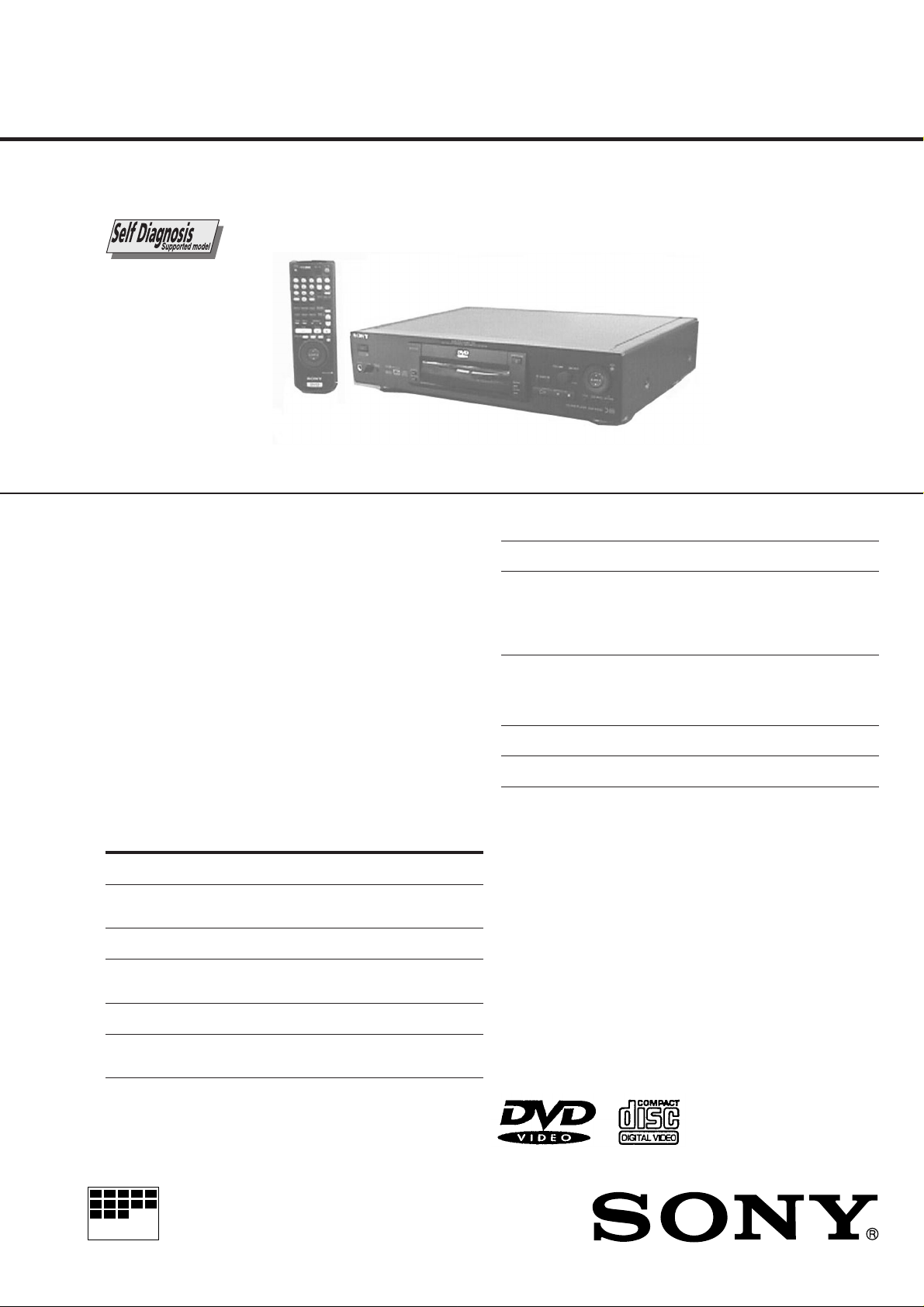
DVP-S525D
/
S725D
RMT-D108P/D111P
SERVICE MANUAL
Photo: DVP-S725D
SPECIFICATIONS
CD/DVD player
Laser Semiconductor laser
Signal format system PAL/(NTSC)
Audio characteristics
Frequency response DVD (PCM 96 kHz): 2 Hz to 44 kHz
(±1 dB)* (S525D)
DVD (PCM 96 kHz): 2 Hz to 44 kHz
(±0.5 dB)* (S725D)
DVD (PCM 48 kHz): 2 Hz to 22 kHz
(±0.5 dB)
CD: 2 Hz to 20 kHz (±0.5 dB)
Signal-to-noise ratio More than 110 dB (LINE OUT (AUDIO)
connectors only) (S525D)
More than 110 dB (AUDIO OUT
connector only) (S725D)
Harmonic distortion Less than 0.0025%
Dynamic range More than 100 dB (DVD)
More than 98 dB (CD)
Wow and flutter Less than detected value
(±0.001% W PEAK)
Outputs and inputs
Jack Output Load impedance
type level
LINE OUT Phono 2 Vrms Over 10 kilohms
(AUDIO) jacks (at 50 kilohms)
(S525D)
AUIO OUT Phono 2 Vrms Over 10 kilohms
(S725D) jacks (at 50 kilohms)
DIGITAL OUT Optical –18 dBm Wave length: 660 nm
(OPTICAL) output
connector
DIGITAL OUT Phono 0.5 Vp-p 75 ohms terminated
(COAXIAL) jack
LINE OUT Phono 1.0 Vp-p 75 ohms,
(VIDEO) jacks sync negative
(S525D)
South African Model
Middle and Near East Model
VIDEO OUT Phono 1.0 Vp-p 75 ohms,
(1, 2) (S725D) jacks sync negative
S VIDEO OUT 4-pin Y: 1.0 Vp-p 75 ohms,
(S525D) mini DIN sync negative
S VIDEO OUT C: 0.3 Vp-p 75 ohms terminated
(1, 2) (S725D) (PAL)
C: 0.286 Vp-p
(NTSC)
COMPONENT phono Y: 1.0 Vp-p 75 ohms,
VIDEO OUT jacks sync negative
(Y, CB/B-Y, CB/B-Y,
CR/R-Y) CR/R-Y:
(S725D) 0.7 Vp-p 75 ohms
PHONES Phone 12 mW 32 ohms
jack
5.1CH Phono 2 Vrms Over 10 kilohms
OUTPUT jacks (at 50 kilohms)
General
Power requirements 220 – 240 V AC, 50/60 Hz
Power consumption 17 W (S525D)
22 W (S725D)
Dimensions (approx.) 430 × 95 × 305 mm (w/h/d)
incl. projecting parts
Mass (approx.) 3.4 kg (S525D)
4.0 kg (S725D)
Operating temperature 5°C to 35°C
Operating humidity 5% to 90%
– Continued on next page –
MICROFILM
CD/DVD PLAYER
Page 2
Supplied accessories
• Audio/Video connecting cord (1)
• S video cable (1)
• Remote commander (remote) RMT-D108P (1)
(S525D)
• Remote commander (remote) RMT -D111P (1)
(S725D)
• Size AA (R6) batteries (2)
DVP-S525D:
* The signals from LINE OUT (AUDIO) connectors and 5.1 ch L, R
connectors are measured. When you play the PCM sound tracks with
96 kHz sampling frequency, the output signals from the DIGITAL OUT
(OPTICAL, COAXIAL) are converted to 48 kHz (sampling frequency).
DVP-S725D:
* The signals from AUDIO OUT connectors and 5.1 ch L, R connectors
are measured. When you play the PCM sound tracks with 96 kHz
sampling frequency, the output signals from the DIGITAL OUT
(OPTICAL, COAXIAL) are converted to 48 kHz (sampling frequency).
Design and specifications are subject to change without notice.
WARNING!!
WHEN SERVICING, DO NO T APPR O A CH THE LASER
EXIT WITH THE EYE TOO CLOSELY. IN CASE IT IS
NECESSARY TO CONFIRM LASER BEAM EMISSION,
BE SURE TO OBSERVE FROM A DISTANCE OF
MORE THAN 25 cm FROM THE SURFACE OF THE
OBJECTIVE LENS ON THE OPTICAL PICK-UP BLOCK.
CAUTION:
The use of optical instrument with this product will increase eye
hazard.
CAUTION
Use of controls or adjustments or performance of procedures
other than those specified herein may result in hazardous radiation exposure.
SAFETY CHECK-OUT
After correcting the original service problem, perform the following
safety checks before releasing the set to the customer:
1. Check the area of your repair for unsoldered or poorly-sol-
dered connections. Check the entire board surface for solder
splashes and bridges.
2. Check the interboard wiring to ensure that no wires are
“pinched” or contact high-wattage resistors.
3. Look for unauthorized replacement parts, particularly transis-
tors, that were installed during a previous repair. Point them
out to the customer and recommend their replacement.
CLASS 3B LASER
LUOKAN 3B LASER
LASERKLASS 3B
4. Look for parts which, though functioning, show obvious signs
of deterioration. Point them out to the customer and recommend their replacement.
5. Check the B+ voltage to see it is at the values specified.
SAFETY-RELATED COMPONENT WARNING!!
COMPONENTS IDENTIFIED BY MARK ! OR DOTTED
LINE WITH MARK ! ON THE SCHEMATIC DIAGRAMS
AND IN THE PARTS LIST ARE CRITICAL TO SAFE
OPERATION. REPLACE THESE COMPONENTS WITH
SONY PARTS WHOSE PART NUMBERS APPEAR AS
SHOWN IN THIS MANUAL OR IN SUPPLEMENTS PUBLISHED BY SONY.
– 2 –
Page 3

TABLE OF CONTENTS
Section Title Page Section Title Page
Service Note ............................................................................ 4
1. GENERAL
Getting Started .............................................................. 1-1
Playing Discs................................................................. 1-4
Using Various Functions with the Control Menu........... 1-6
Settings and Adjustments ............................................. 1-12
2. DISASSEMBLY
2-1. Case Removal ............................................................... 2-1
2-2. MB-85 Board Removal.................................................. 2-1
2-3. Power Block Removal ................................................... 2-1
2-4. ER-4/5 Board Removal ................................................. 2-1
2-5. AU-209 Board Removal (S525D) ................................. 2-2
2-6. AU-211 Board Removal (S725D) .................................. 2-2
2-7. Tray Cover Removal ..................................................... 2-2
2-8. Front Panel Removal .................................................... 2-2
2-9. Mechanism Deck Removal ........................................... 2-3
2-10. Tray Removal ................................................................ 2 -3
2-11. Optical Pick-up Removal ............................................... 2-3
2-12. Belt, Loading Motor (M001),
MS-29/TK-54 Board Removal....................................... 2-3
2-13. Internal View.................................................................. 2-4
2-14. Circuit Boards Location................................................. 2-5
3. BLOCK DIAGRAMS
3-1. Overall Block Diagram .................................................. 3-1
3-2. RF/Servo Block Diagram .............................................. 3-3
3-3. Signal Process Block Diagram ..................................... 3-5
3-4. Video Block Diagram..................................................... 3-7
3-5. System Control Block Diagram ..................................... 3-9
3-6. Audio (1) Block Diagram ............................................... 3-11
3-7. Audio (2) Block Diagram ............................................... 3-13
3-8. Audio (3) Block Diagram ............................................... 3-15
3-9. Interface Control Block Diagram................................... 3-17
3-10. Power Block Diagram.................................................... 3-19
4. PRINTED WIRING BOARDS AND SCHEMATIC
DIAGRAMS
4-1. Frame Schematic Diagrams.......................................... 4-3
FRAME (1) Schematic Diagram.................................... 4-3
FRAME (2) Schematic Diagram.................................... 4-5
FRAME (3) Schematic Diagram.................................... 4-7
4-2. Printed Wiring Boards and Schematic Diagrams ......... 4-9
TK-54 Printed Wiring Board .......................................... 4-9
TK-54 Schematic Diagram ............................................ 4-13
MS-29 Printed Wiring Board and
Schematic Diagram ....................................................... 4-15
MB-85 Printed Wiring Board ......................................... 4-17
MB-85 (AV DECODER) Schematic Diagram................ 4-21
MB-85 (SDRAM) Schematic Diagram .......................... 4-23
MB-85 (SERVO DSP) Schematic Diagram .................. 4-25
MB-85 (DRIVE) Schematic Diagram ............................ 4-27
MB-85 (ARP) Schematic Diagram ................................ 4-29
MB-85 (SYSTEM CONTROL)
Schematic Diagram ....................................................... 4-31
MB-85 (HGA) Schematic Diagram................................ 4-33
MB-85 (CLOCK GENERATOR, AUDIO DSP,
V EQ/NR) Schematic Diagram...................................... 4-35
MB-85 (DAC) Schematic Diagram ................................ 4-37
MB-85 (BIAS) Schematic Diagram ............................... 4-39
AU-211 Printed Wiring Board........................................ 4-41
AU-211 (AUDIO) Schematic Diagram........................... 4-45
AU-211 (VIDEO BUFFER) Schematic Diagram ........... 4-47
AU-209 Printed Wiring Board ....................................... 4-49
AU-209 (AUDIO) Schematic Diagram .......................... 4-51
AU-209 (VIDEO BUFFER) Schematic Diagram........... 4-53
ER-4 Printed Wiring Board............................................ 4-55
ER-4 (EURO AV1) Schematic Diagram ........................ 4-57
ER-4 (EURO AV2) Schematic Diagram ........................ 4-59
ER-5 Printed Wiring Board............................................ 4-61
ER-5 (EURO AV1) Schematic Diagram ........................ 4-65
ER-5 (EURO AV2) Schematic Diagram ........................ 4-67
FL-100 Printed Wiring Board ........................................ 4-69
FL-98 Printed Wiring Board .......................................... 4-73
FL-98/100 (FUNCTION SWITCH)
Schematic Diagram....................................................... 4-75
FL-98/100 (IF CON) Schematic Diagram ..................... 4-77
SW-314/316 Printed Wiring Boards.............................. 4-79
FR-147/149 Printed Wiring Boards............................... 4-80
SW-314/316, FR-147/149 Schematic Diagram............ 4-81
HP-108/110 Printed Wiring Boards and
Schematic Diagram....................................................... 4-83
RY-12 Printed Wiring Board and
Schematic Diagram....................................................... 4-85
HS-030SH Printed Wiring Board .................................. 4-87
HS-030SH Schematic Diagram .................................... 4-89
5. IC PIN FUNCTION DESCRIPTION
5-1. System Control Pin Function
(MB-85 Board IC202) .................................................... 5-1
6. TEST MODE
6-1. General Description ...................................................... 6-1
6-2. Starting Test Mode ........................................................ 6-1
6-3. Syscon Diagnosis.......................................................... 6-1
6-4. Drive Auto Adjustment .................................................. 6-5
6-5. Drive Manual Operation ................................................ 6-7
6-6. Mecha Aging ................................................................. 6-9
6-7. Emergency History ........................................................ 6-9
6-8. Version Information ....................................................... 6-10
6-9. Video Level Adjustment ................................................ 6-10
6-10. If Con Self Diagnostic Function .................................... 6-11
7. ELECTRICAL ADJUSTMENT
7-1. Power Supply Adjustment ............................................. 7-1
1. HS030SH Board............................................................ 7-1
7-2. Adjustment of Video System......................................... 7-2
1. Video Level Adjustment................................................. 7-2
2. S-terminal Output Check............................................... 7-2
3. Checking Component Video Output B-Y...................... 7-2
4. Checking Component Video Output R-Y...................... 7-2
5. Checking Component Video Output Y.......................... 7-3
6. Checking RGB Output R ............................................... 7-3
7. Checking RGB Output G............................................... 7-3
8. Checking RGB Output B ............................................... 7-3
9. Checking S Video output S-C ....................................... 7-4
7-3. Adjustment Related Parts Arrangement ....................... 7-6
8. REPAIR PARTS LIST
8-1. Exploded Views............................................................. 8-1
8-1-1. Case Assembly (S525D).......................................... 8-1
8-1-2. Case Assembly (S725D).......................................... 8-2
8-1-3. Front Panel Assembly .............................................. 8-3
8-1-4. Chassis Assembly .................................................... 8-4
8-1-5. Mechanism Deck Assembly..................................... 8-6
8-2. Electrical Parts List........................................................ 8-7
– 3 –
Page 4
SERVICE NOTE
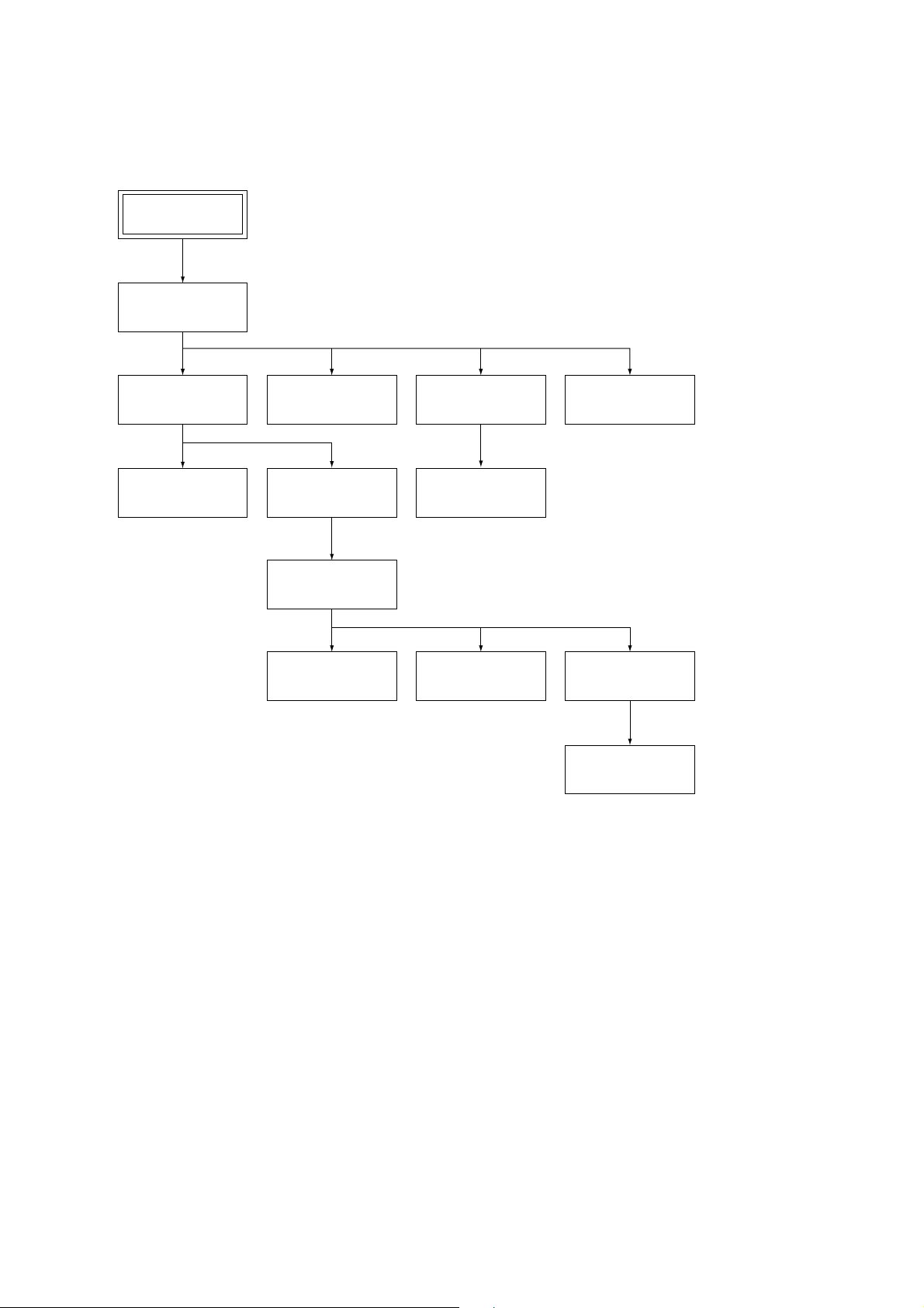
1. DISASSEMBLY
• This set can be disassembled in the order shown below.
Set
Case
(Page 2-1)
Tray Cover
(Page 2-2)
Front Panel
(Page 2-2)
MB-85 Board
(Page 2-1)
Mechanism Deck
(Page 2-3)
Tray
(Page 2-3)
Optical Pick-up
(Page 2-3)
ER-4/5 Board
(Page 2-1)
AU-209/211 Board
(Page 2-2)
TK-54 Board
(Page 2-3)
Power Block
(Page 2-1)
Belt
(Page 2-3)
Loading Motor (M001),
MS-29 Board
(Page 2-3)
– 4 –
Page 5
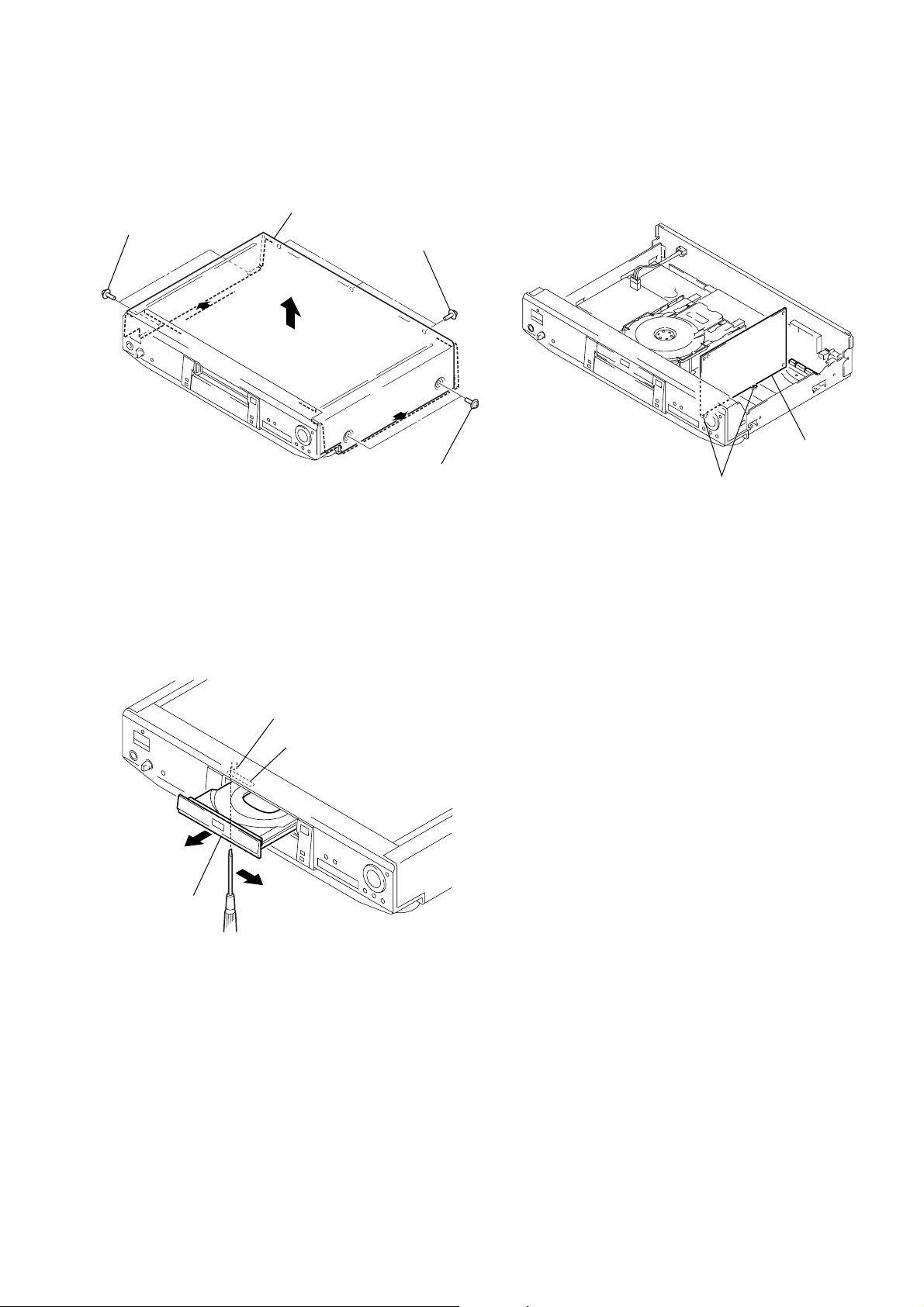
2. NOTE ON REMOVE THE CASE
1) Remove seven screws. (See Fig. 1)
2) Open the side of case. (See Fig. 1)
3) Remove the case as lift straight. (See Fig. 1)
Case
Two screws
Three screws
Two screws
Fig. 1
3. DISC REMOVAL PROCEDURE
(at POWER OFF)
1) Insert a tapering driver into the aperture of the unit bottom,
and move the lever of chuck cam in the direction of the arrow
A. (See Fig. 2)
2) Draw out the tray in the direction of the arrow B, and remove
a disc. (See Fig. 2)
4. HOW TO SERVICE MB-85 BOARD
1) Remove the case from the set. (Refer to 2-1)
2) Remove the MB-85 board. (Refer to 2-2)
3) Set the MB-85 board as shown in Fig. 3.
Note: Do not disconnect wiring, except FMA-7/8/9.
MB-85 board
grooves
Fig. 3
B
Lever of chuck cam
Aperture
A
Tray
Fig. 2
– 5 –
Page 6
SECTION 1
GENERAL
DVP-S525D/S725D
This section is extracted from DVP-S725D
instruction manual (3-866-153-21).
1-1
Page 7
1-2
Page 8
1-3
Page 9
1-4
Page 10
1-5
Page 11
1-6
Page 12
1-7
Page 13
1-8
Page 14
1-9
Page 15
1-10
Page 16
1-11
Page 17
1-12
Page 18
1-13
Page 19
1-14
Page 20
1-15
Page 21
1-16
Page 22

1-17 E
1-17
Page 23
SECTION 2
2 Connector
(CN101)
3 Three connectors
(CN201, 202, 203)
1 Connector
(CN102)
(S725D)
4 Four screws
(B3)
5 Power block
2 Four screws
(B3)
1 Two flat cables
(CN901, 902)
3 ER-4 board (S525D)
ER-5 board (S725D)
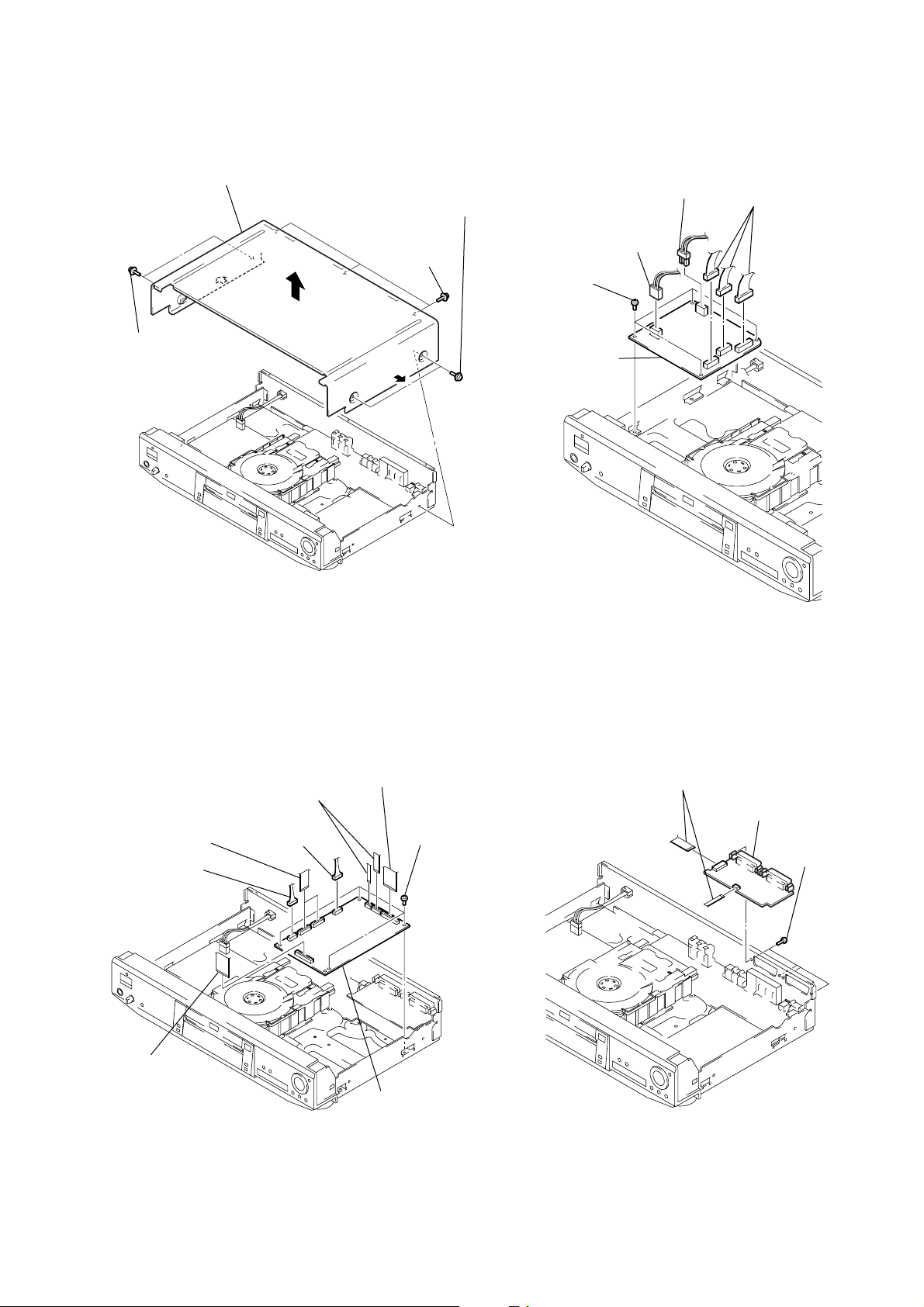
DISASSEMBLY
Note: Follow the disassembly procedure in the numerical order given.
2-1. CASE REMOVAL
4 Case
2 Two screws
1 Three screws
3 Two screws
DVP-S525D/S725D
2-3. POWER BLOCK REMOVAL
2-2. MB-85 BOARD REMOVAL
4 Two flat cables
(CN004, 007)
2 Two flat cables
(CN002, 003)
1 Connector
6 Flat cable
(CN006)
(CN011)
3 Connector
(CN001)
2-4. ER-4/5 BOARD REMOVAL
5 Flat cable
(CN005)
7 Four screws
(B3)
8 MB-85 board
2-1
Page 24
2-5. AU-209 BOARD REMOVAL
(S525D)
2-7. TRAY COVER REMOVAL
7 Three screws
(B3)
2 Connector
(CN401)
1 Connector
(CN201)
4 Flat cable
(CN302)
3 Flat cable
(CN301)
8 AU-209 board
5 Five screws
(B3)
6 Two screws
(B3)
4 Tray cover
B
2 Pull the tray in the
direction of the
arrow B.
1 Insert a tapering driver into the aperture of the
unit bottom, and move the lever of chuck cam
in the direction of the arrow A.
3 Two claws
A
2-6. AU-211 BOARD REMOVAL
(S725D)
6 Three screws
(B3)
2 Connector
(CN401)
3 Two connectors
(CN301, 404)
4 Three flat cables
(CN402, 403, 405)
7 AU-211 board
5 Nine screws
(B3)
2-8. FRONT PANEL REMOVAL
4 Screw
(B3)
2 Connector
(CN701)
5 Two screws
(B3)
9 Claw
0 Front panel
6 Boss
1 Connector
(CN203)
8 Claw
7 Boss
3 Flat cable
(CN006)
1 Connector
(CN407)
2-2
Page 25
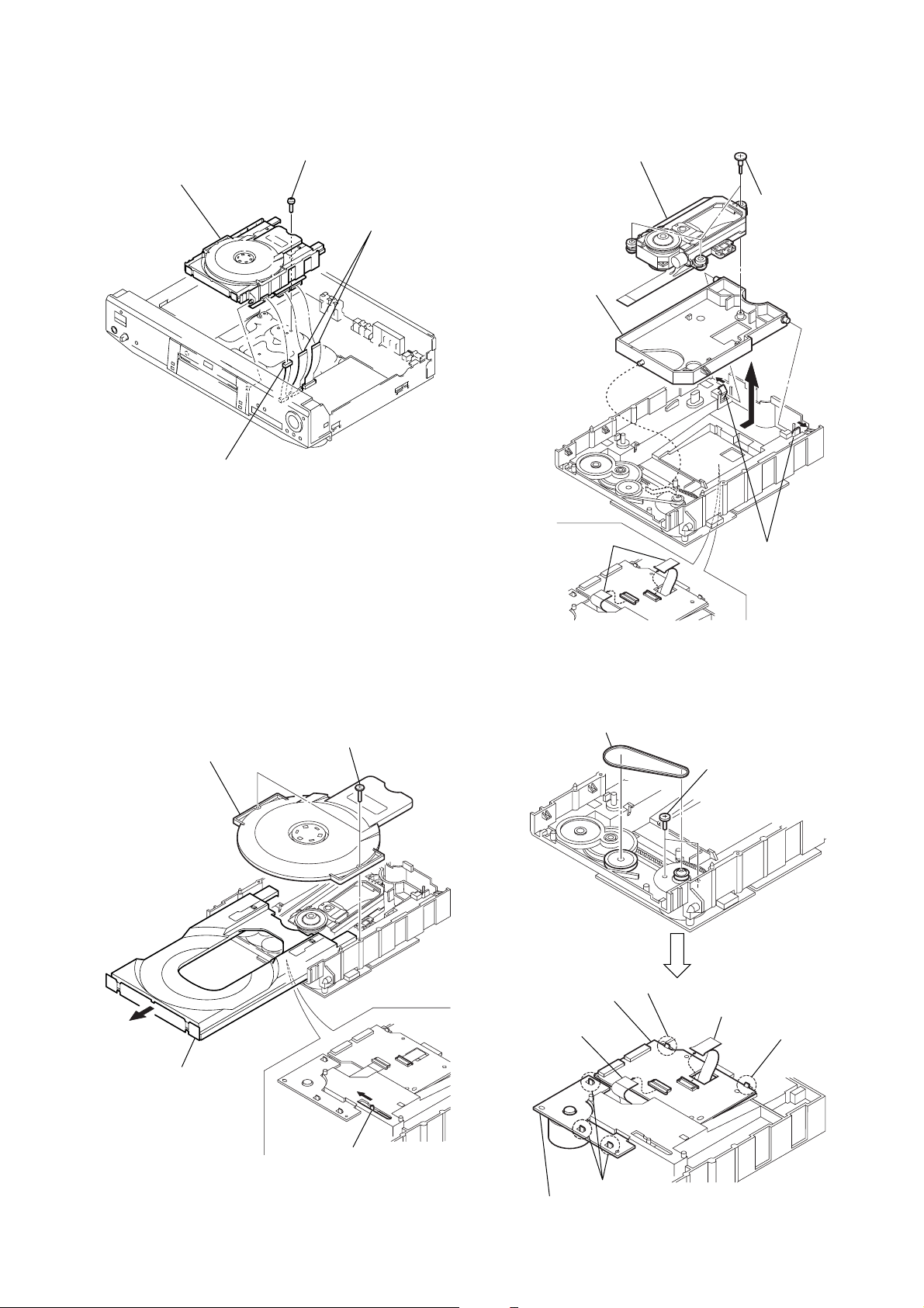
2-9. MECHANISM DECK REMOVAL
2-11. OPTICAL PICK-UP REMOVAL
4 Mechanism deck
1 Connector
(CN001)
3 Screw
(B3)
2 Two flat cables
(CN003, 004)
5 Optical pick-up
3 Remove the base
unit holder in the
direction of the
arrow A.
1 Two flexible board
(CN001, 002)
4 Three step
screws
A
2 Two claws
2-10. TRAY REMOVAL
2 Chuck ass’y
B
4 Remove the tray in
the direction of the
arrow B.
1 Two screws
(BTP2.6 × 12)
A
2-12. BELT, LOADING MOTOR (M001),
MS-29/TK-54 BOARD REMOVAL
1 Belt
2 Two screws
(B2.6 × 4)
9 TK-54 board
5 Flexible board
(CN002)
8 Claw
6 Flexible board
(CN001)
7 Claw
3 Move the lever of chuck cam
in the direction of the arrow A.
3 Three claws
4 Loading motor (M001),
MS-29 board
2-3
Page 26
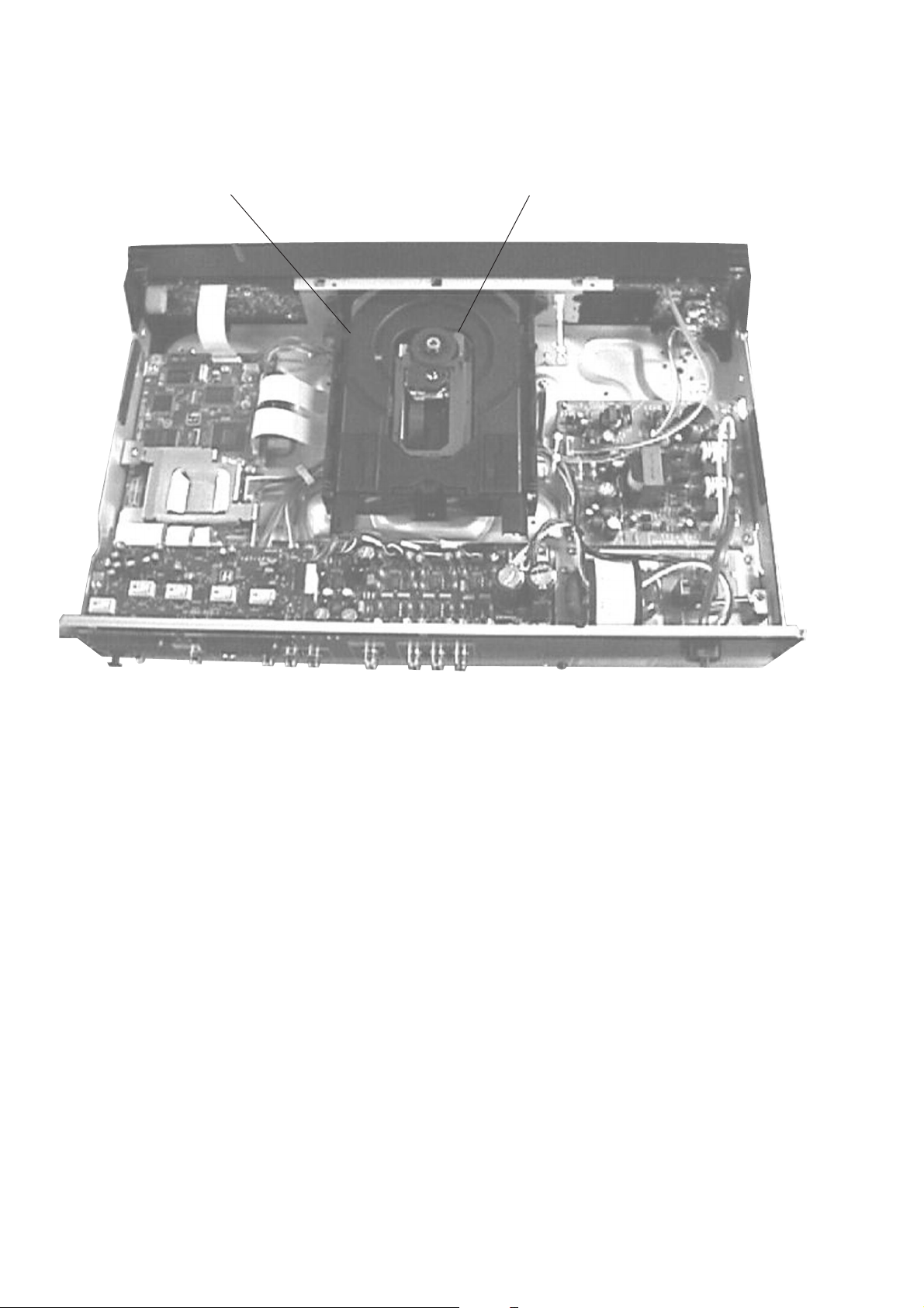
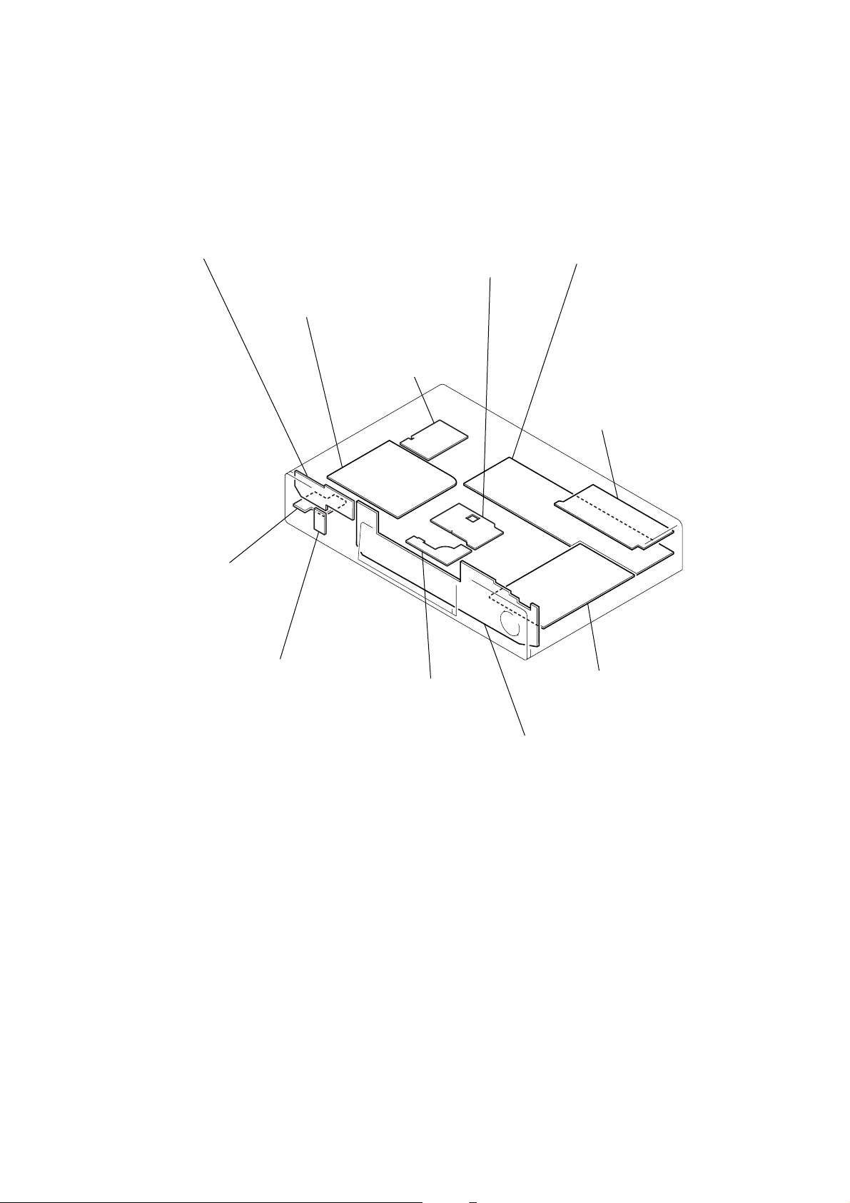
2-13. INTERNAL VIEW
DC motor (loading)
1-541-632-11
Optical pick-up (KHM-220AAA/J1RP)
8-820-081-03
2-4
Page 27
2-14. CIRCUIT BOARDS LOCATION
FR-147 (S525D)
FR-149 (S725D)
(IR/POWER SWITCH)
Power Block (HS-030SH)
(SWITCHING REGULATOR)
HP-108 (S525D)
HP-110 (S725D)
(HEADPHONE)
TK-54
(RF/SERVO)
RY-12 (S725D)
(RELAY)
AU-209 (S525D)
AU-211 (S725D)
(AUDIO)
ER-4 (S525D)
ER-5 (S725D)
(EURO AV)
SW-314 (S525D)
SW-316 (S725D)
(SURROUND SWITCH)
MS-29
(LOADING)
MB-85
(SIGNAL PROCESS/SERVO)
FL-98 (S525D)
FL-100 (S725D)
(FUNCTION SWITCH)
2-5 E
2-5
Page 28
3-1. OVERALL BLOCK DIAGRAM
DVP-S525D/S725D
SECTION 3
BLOCK DIAGRAMS
BASE UNIT
KHM-220AAA
OPTICAL DEVICE
DVD/CD
FOCUS
TRACKING
TILT
MOTOR
PDIC
COIL
COIL
MB-85 BOARD
(SEE PAGE 4-21 to 39)
IC304
16M DRAM
TK-54 BOARD
(SEE PAGE 4-13)
SD 0-7
RF
IC001
DVD/CD RF AMP
DIGITAL SERVO
IC801
FOCUS COIL/
TRACKING COIL/
TILT MOTOR
DRIVE
M
DVD RF,
CD RF
IC303
ARP2
IC701
SERVO DSP
CDDOUT, CDDATA,
CDBCK, CDLRCK
IC601
HGA
IC402, 403
16M SDRAM
S725D
IC401
AV DECODER
IC202
SYSTEM CONTROL
V EQ/NR
PDO 0-7
IC502
Parallel BUS
PDI 0-7
SPDIF, ACH12,
ACH34, ACH56,
BCK, LRCK
IC204
1M SRAM
IC201
4K EEP ROM
IC501
AUDIO DSP
IC206
16M FLASH
VIDEO Y,
VIDEO B-Y,
VIDEO R-Y
VIDEO V,
VIDEO Y,
VIDEO C
VIDEO R,
VIDEO G,
VIDEO B
SPDIF
IC902
AUDIO 2CH DAC
AU-209/211 BOARD
(SEE PAGE 4-45, 47, 51, 53)
VIDEO
BUFFER
VIDEO
BUFFER
ER-4/5 BOARD
(SEE PAGE 4-57, 59, 65, 67)
AUDIO LT,
AUDIO RT
LPF,
GAIN CONTROL
IC901-903
RY901-903
SW, BUFFER
RY904, 905
SW
COMPONENT
VIDEO
VIDEO
S VIDEO
EURO AV1
(RGB)-TV
EURO AV2
DIGITAL
OUT
AUDIO
OUT
SPINDLE
MOTOR
SLED
MOTOR
M001
LOADING
MOTOR
MS-29 BOARD
(SEE PAGE 4-16)
05
IC201
IF CON
Serial BUS
SWITCH
FR-147/149 BOARD
(SEE PAGE 4-81)
–12V
EVER5V
JOG UNIT
IC905-907
AUDIO 5.1CH DAC
+3.3V
+5V
A+12V
M+12V
AUDIO L, R
AUDIO LS, RS
AUDIO C, LFE
+3.3V
+5V
+12V
–12V
EVER5V
HS-030SH BOARD
(SEE PAGE 4-89)
HEADPHONE
AMP
LPF
S725D
HP-108/110
BOARD
(SEE PAGE 4-84)
RY-12 BOARD
(SEE PAGE 4-86)
SW REG
PHONES
5.1CH OUTPUT
AC10V
T901
M
M
IC802
SPINDLE/SLED/
LOADING
MOTOR DRIVE
S725D
IC602
16M NAND-F
M
ND201
FL-98/100 BOARD
(SEE PAGE 4-75, 77)
SWITCH SWITCH
SW-314/316 BOARD
(SEE PAGE 4-81)
3-1 3-2
Page 29
DVP-S525D/S725D
3-2. RF/SERVO BLOCK DIAGRAM
IC0011(DVD play)
200mV/DIV 100ns/DIV
536mVp-p
BASE UNIT
KHM-220AAA
OPTICAL DEVICE
DVD/CD
PDIC
DVD/CD
LD MODULE
COIL
TRACKING
COIL
TILT
M
MOTOR
INLIMIT
SENSOR
IC0011(CD play)
500mV/DIV 500ns/DIV
880mVp-p
RF
7
9
A-D
10
16
17
8
E-H
11
15
18
VC
13
PD
4
LD
2
VR
5
FCSFOCUS
19
20
TRK
21
22
10
TIA, TIB
ı
13
INLIM
2
TK-54 BOARD
(SEE PAGE 4-13)
CN001
Q001
LD DRIVE
CN002
IC001%¢(DVD play)
500mV/DIV 100ns/DIV
1.5Vp-p
IC001
DVD/CD RF AMP
DIGITAL SERVO
RF IP
1
9
ı
A-D
12
5
ı
A2-D2
8
13
E-H
ı
16
VC
17
19
PD
20
LD
IC001@ª(DVD play)
200mV/DIV 500ms/DIV
592mVp-p
IC001%¢(CD play)
500mV/DIV 500ns/DIV
1.5Vp-p
54
SIGO
40
FE
39
TE
29
PI
26
MIRR
32
TZC
33
VCI
SCLK
43
SWD
ı
SRD
46
SDEN
27
FDCHG
42
HOLD2
31
DFT
IC001@ª(CD play)
200mV/DIV 20ms/DIV
448mVp-p
Q002
CN004
17
9
8
7
3
5
6
SSCK, SSWD,
11
SSRD, SSCS
ı
14
15
4
6
7
4
5
15
ı
18
8
RF+
FE
TE
PI
MIRR
TZC
2VC
SSDFCT
SSDFCTI
FCS
TRK
TIA, TIB
INLIM
IC001$º(DVD play)
100mV/DIV 50ms/DIV
180mVp-p
MB-85 BOARD (1/7)
(SEE PAGE 4-25, 27)
CN002CN003
2
10
11
12
500mV/DIV 50ms/DIV
16
14
13
5
8
4
15
12
13
14
15
1
4
11
2VC
ı
CN003
ı
500mV/DIV 50ms/DIV
IC001#ª(DVD play)
1.3Vp-p
IC001$º(CD play)
860mVp-p
IC001#ª(CD play)
500mV/DIV 200ms/DIV
1.7Vp-p
IC801
FOCUS
13
14
DRIVE
TRACKING
11
12
DRIVE
15
ı
MOTOR
18
DRIVE
IC802
COIL
COIL
TILT
23
26
2
3
9
5
6
7
20
TLTA, TLTB
IC701^ª(DVD play)
500mV/DIV 50ms/DIV
1.4Vp-p
FCD
TRD
IC701^ª(CD play)
500mV/DIV 200ms/DIV
1.7Vp-p
Q801
IC702 (1/2)
3 1
IC803 (1/2)
12
13
14
FCD
TRD
TLTA, TLTB
SLDA, SLDB,
STVC
TILT MUTE
FGMODE
IC701^•(CD play)
500mV/DIV 50ms/DIV
860mVp-p
68
ADC1
69
ADC0
67
ADC2
66
ADC3
65
ADC4
21
TRIN
20
TRREF
23
FGIN
41
GIO 5-8
ı
44
38
GIO 11
28
DFCTI
80
DAB 2, 3
85
92
DAB 0, 1
97
48
GIO 1, 2
49
7
PWM 0-2
ı
9
46
GIO 4
50
GIO 0
IC701^•(DVD play)
100mV/DIV 5ms/DIV
IC701
SERVO DSP
RS
26 108
180mVp-p
X2/CLKIN
FG REF
VRBA,
DAB 0-3
GIO 10
HINT
HRD
HWR
HCS
EA 0, 1
HD 0-7
DVD RF
CD RF
SIGNAL
22
74
81
84
93
96
39
128
1
2
3
4
5
117
ı
120
122
125
IC702 (2/2)
7 5
LOCK
MDS0
MDP0
FCSON
XSDPIT
XSDPRD
XSDPWR
XSDPCS
HA0, 1
HD8-15
N27MSDP
XSDPRST
X3VRST
PROCESS
(SEE PAGE 3-5)
+3.3V
SYSTEM
CONTROL
(SEE PAGE 3-9, 10)
SPINDLE
5
6
7
ı
10
1
2
4
6
3
CN011
OCSW 1, 2
CKSW1
CN001
13
14
9
ı
12
1
2
4
6
3
SPM
SLA, SLB
LDM
OCSW 1, 2
CKSW1
8
SPINDLE
05
MOTOR
SLED
MOTOR
M
M
SPM
SLA, SLB
9
4
ı
7
MS-29 BOARD
(SEE PAGE 4-16)
M001
LOADING
MOTOR
TRAY SENSOR
CHUCK SENSOR
M
S001
S002
15
MOTOR
16
DRIVE
11
14
17
18
SLED
ı
MOTOR
DRIVE
LOADING
MOTOR
DRIVE
26
20
2
3
5
6
9
23
SLDA, SLDB,
STVC
+3.3V
+5V
IC803 (2/2)
5 7
10
3 1
2.5VC
8
2VC
1.6VC
Q802, 803
GAIN
CONTROL
SPDLSTOP
SPGAIN
XDRVMUTE
LDMM/DMM
LDMP/DMP
OCSW1
OCSW2
CKSW1
3-3 3-4
Page 30
3-3. SIGNAL PROCESS BLOCK DIAGRAM
DVP-S525D/S725D
MB-85 BOARD (2/7)
(SEE PAGE 4-21, 23, 29, 35)
IC303!ª(CD play)
500mV/DIV 200ns/DIV
RF, SERVO
(SEE PAGE 3-4)
SYSTEM
CONTROL
(SEE PAGE 3-9, 10)
1.6Vp-p
DVD RF
CD RF
MDS0
MDP0
LOCK
DFCT
NORF
LOCK
FWON
MD2
MUTE
XARPWR
XARPRD
XARPIT
XARPCS
XARPWT
XCS2
XCS3
XRD
XWRH
XAVDIT
XAVDWT
DACK0
DREQ0
DACK1
DREQ1
IC303!¶(DVD play)
500mV/DIV 100ns/DIV
1.6Vp-p
S725D
IC502
V EQ/NR
IC304
16M DRAM
MA 0-9
MD 00-15
154-157
136-139
159-162
141-144
164-167
RFIN1
RFIN2
MDS0
MDP0
DFCT
NORF
LOCK
FWON
MD2
MUTE
XWR
XRD
XINT
XCS
XWAT
XRST
87
121
XARPRST
33MARP
146 147
MCKI
123
169-172
IC303
ARP2
SCKI
73-76 79-82
17
19
49
52
55
56
58
59
113
111
60
61
83
84
86
A 0-7
XRAS, XOE
XMWR, XCAS,
148
150-152
63-68 70 71
SD 0-7
D 0-7
97
SD 0-7
98
100
ı
105
SDCK, SDEF,
91
XSHD, XSAK, XSRQ
93
ı
96
CDDOUT, CDDATA,
107
CDBCK, CDLRCK
ı
110
38
ı
43
45
46
47
ı
51
29
ı
32
166
167
193
194
196
198
ı
202
DAD 0-11
105-108
110-113
115-118
DT 0-7 I
103 19 36
XAVDRST
RSTIN
256FS30
ACLKIN
IC402, 403
16M SDRAM
DDT 0-15
134 135
137 138
140 141
143 144
146 147
149 150
152 153
155 156
CRPCLKIN
CLKI
160 163
27M30
33M30
YI 0-7
CLK, CKE,
DQML, DQMU,
CS, WE, CAS, RAS
120-123
125 127
129-132
SCLKIN
168-170 172-178 180-187 189-192 2-5 7-10 12-15 205-208
PDO 0-7
PDO 0-7
IC401%
728mVp-p(H)
IC401
AV DECODER
HAD 0-21 I
YO 0-7
60-6711-18
PDI 0-7
75-78 80-8386-89 91-94
PDI 0-7
IC401%¶(RGB output)
728mVp-p(H)
IC401^∞
1.2Vp-p(H)
IC401^¡
1.1Vp-p(H)
IC401^™
816mVp-p(H)
HSYNC
FLD
SDI
97 98
31 29
FLDO
SDOUT
HSYNCO
72 73 98 99
FLDO
HSYNCON
NR-SDOUT
HD 0-15
CLK
RST
CS
SENO
NR-SENO
100
93
G/Y OUT
R/B-Y OUT
B/R-Y OUT
COMP OUT
ACH12O
ACH34O
ACH56O
IC401%•(RGB output)
58
54
57
65
61
Y OUT
62
C OUT
21
22
23
25
LRCKO
26
BCKO
VREFI
70
RV401
VIDEO
LEVEL
1.0Vp-p(H)
IC401%•
1.0Vp-p(H)
ADJ
X57RST
27M57
IC401%¢(RGB output)
720mVp-p(H)
IC401%¢
720mVp-p(H)
VIDEO G/Y
VIDEO R/B-Y
VIDEO B/R-Y
VIDEO V
VIDEO Y
VIDEO C
VIDEO
(SEE PAGE 3-7)
XARPRST
XAVDRST
X57RST
S725D
33MARP
256FS30
33M30
27M30
27M57
S725D
HA 0-7
HA 0-21
HD 0-15
05
HD 8-15
CDDOUT, CDDATA, CDBCK, CDLRCK
HA 0-21
HD 0-15
ACH12
ACH34
ACH56
LRCK
BCK
CDDOUT
CDDATA
CDBCK
CDLRCK
AUDIO 1
(SEE PAGE 3-11)
3-5 3-6
Page 31

DVP-S525D/S725D
3-4. VIDEO BLOCK DIAGRAM
MB-85 BOARD (3/7)
(SEE PAGE 4-21, 37)
SIGNAL
PROCESS
(SEE PAGE 3-6)
INTERFACE
CONTROL
(SEE PAGE 3-18)
SYSTEM
CONTROL
(SEE PAGE 3-9, 10)
05
VIDEO G/Y
VIDEO R/B-Y
VIDEO B/R-Y
VIDEO V
VIDEO Y
VIDEO C
V MUTE
DISC/EXT
RGB
EURO V/Y
AU-209/211 BOARD (1/2)
S725D
CN004
4
2
6
7
1
CN005
1
3
5
8
VS
6 23
18
VIDEO G/Y
VIDEO R/B-Y
VIDEO B/R-Y
RGB
EURO V/Y
EURO V/Y
YUV
VIDEO B
VIDEO R
VIDEO G
VIDEO V
VIDEO Y
VIDEO C
V MUTE
VS
DISC/EXT
(SEE PAGE 4-45, 47, 51, 53)
CN405
4
6
2
1
7
1
7
6
2
4
CN406
IC301,3212
1.1Vp-p(H)
28
26
24
21
11
CN402: S725D
CN301: S525D
Q439, 440
RGB/YUV SW
Q301, 302
BUFFER
IC301,3217
860mVp-p(H)
IC301,321!∞
2.0Vp-p(H)
VIDEO R
VIDEO G
VIDEO B
EURO V/Y
YUV
IC301,3214
1.2Vp-p(H)
VIDEO BUFFER
2
7 10
1
Q301, 302: S725D
Q321, 322: S525D
IC301,3210
1.8mVp-p(H)
CN901
2
4
6
1
7
ER-4/5 BOARD (1/2)
(SEE PAGE 4-57, 59, 65, 67)
IC301
IC321
DC ON/OFF
AUDIO 2
(SEE PAGE 3-14)
AUDIO 3
(SEE PAGE 3-16)
IC302
VIDEO BUFFER
2 15
4
7 10
1
IC301,321!£
2.4 Vp-p(H)
: S725D
: S525D
134
15
CN302: S725D
CN305: S525D
: S525D
: S725D
13
RELAY DRIVE CONT
17
15
13
3
4
6
VIDEO V
VIDEO Y
VIDEO C
V MUTE
VS
DISC/EXT
J302
J309: S725D
J506: S525D
VIDEO OUT
J308: S725D
J507: S525D
Y
C
CN902
17
15
13
3
4
6
Y
B/B-Y
C
C
R/R-Y
S VIDEO OUT
COMPONENT
VIDEO OUT
3
1
IC903
SWITCH
SWITCH
1
3
Q917
S725D
IC902
2
2
Q918
MUTE CONT
7
7
VIDEO BUFFER
2 15
4 13
7 10
1
Q909, 910
RELAY DRIVE
CONT
Q906-908
AV CONT GEN
Q901-903
I SIG GEN
IC901
MUTE
RY903
RY901
RY902
7
4
7
4
7
4
9
2 1
Q914
RELAY DRIVE
29
1
Q912
RELAY DRIVE
9
2 1
Q913
RELAY DRIVE
V/Y IN
20
V/Y OUT
19
R/C OUT
15
8
3
8
3
8
3
AV CONT OUT
Q904, 905
I SIG SW
AV CONT IN
G OUT
B OUT
I OUT
V IN
V OUT
R IN
G IN
B IN
I IN
CN904
11
EURO AV1
(RGB)-TV
7
8
16
20
19
15
11
CN903
EURO AV2
7
16
8
3-7 3-8
Page 32

3-5. SYSTEM CONTROL BLOCK DIAGRAM
DVP-S525D/S725D
MB-85 BOARD (4/7)
(SEE PAGE 4-31, 33, 35)
SIGNAL
PROCESS
(SEE PAGE 3-5)
RF, SERVO
(SEE PAGE 3-4)
AUDIO 2
: S525D
(SEE PAGE 3-13)
AUDIO 3
: S725D
(SEE PAGE 3-15)
IC202(™
2.4Vp-p(12.5MHz)
05
HA 0-21
HD 0-15
HA 0, 1
HD 8-15
X3VRST
GAIN2
GAIN2
X201
12.5MHz
X001
27MHz
IC0016
4.2Vp-p(27.0MHz)
HA 0-21
42 44-64
3
PB7/DW1
91
X1
92
X0
A22/P66
RAS1/PB4
66 100 99 98
CKSEL
DVD/CD
DVD:5.8Vp-p(36.5MHz)
19
1
6
4.6Vp-p(33.8MHz)
A 01-15
IC001!
CD:5.1Vp-p
MD
ML
XT1
IC001!™
HD 0-15
25-39 41
D 16-31
SYSTEM CONTROL
IC001!¢(DVD play)
4.2Vp-p(25.3MHz)
IC001!¢(CDplay)
4.7Vp-p(22.5MHz)
IC001
PLL
SCKO3
17
14
SCKO2
12
SCKO1
SI1
SIO
SC0
SO0
76 77 78 79 80 89 14 97
SI0
SO0
IC202
3 5
6 2
1 7
SO1
SI1
SC0
SO1
IC2025
4Vp-p(25.3MHz)
DW0/PB3
CS0H/PB2
1
3
IC004
SC1
SC1
PF7/OCPA0/ATG
DVD:6.2Vp-p(37.0MHz)
CD:5Vp-p(33.6MHz)
IC003
IC0042,5,7
4.2Vp-p(26.9MHz)
HA 1-16
CS0L
XFRRST
RST
CS0L
11
CS0
10
CS1
7
CS4
22
RD
23
WR0
24
WR1
19
RDY
94
INT1
88
INT3
83
5
CLK
9
CS2
8
CS3
95
INT0
84
DACK1
85
DACK0
86
DREQ1
87
DREQ0
RAS0/PB0 DISC/EXT
IC0035,7
85
7
5
IC207
POWER ON
4 5
RESET
XDACS0
XDACS1
384FSDA
384FS01
27M01
256FS30
33MARP
33M30
S725D
27M57
27M30
N27MSDP
XRD
XWRH
XCS2
XCS3
XAVDIT
DACK1
DACK0
DREQ1
DREQ0
AUDIO 1
(SEE PAGE 3-11)
SIGNAL PROCESS
(SEE PAGE 3-5)
RF, SERVO
(SEE PAGE 3-4)
IC204
1M SRAM
HD 0-15
+3.3V
CE
WE
CS
SIGNAL PROCESS
(SEE PAGE 3-5)
VIDEO
(SEE PAGE 3-7)
CS, WE,
OE, UB, LB
SIGNAL PROCESS
(SEE PAGE 3-5)
HA 1-20
SC0
SO0
SI0
VIDEO
(SEE PAGE 3-7)
IC206
16M FLASH
WE,
HD 0-15
IC201
4K EEPROM
4 3
5 8
6 1
SK
DI
DO
FWON
XARPRST
XARPIT
XARPWT
XARPWR
XARPRD
XARPCS
XAVDWT
XAVDRST
X57RST
S725D
EURO V/Y
CS
WC
R/B
MUTE
MD2
NORF
DFCT
LOCK
VS
RGB
N27MHGA
OE, CE
WE, UB, LB, OE
23
24
25
112
113
124
125
141
142
145
144
143
157
156
155
3
135
98
99
102
103
104
105
106
107
108
109
110
111
72
71
27
53
52
51
59
XECS
XEWC
XEBSY
CS1
CS4
HRD
HWRH
HWRL
WAIT
XINT1
XINT3
RST
CPUCK
MUTE
MD2
NORF
DFCT
FWON
LOCK
ARPRST
ARPINT
ARPWT
ARPWR
ARPRD
ARPCS
AVDWT
AVDRST
57RST
VS
RGB SEL
EURO V/Y
MCK
HA 0-5, 17-19
HA 0-5, 17-19
IC601
HGA
HD 8-15
126-133146-154
HD 0-7
LDMM/DMM
NFD 0-7
XIFINT
FCSON
SDPRST
SDPIT
SDPWR
SDPRD
SDPCS
SPDLSTOP
SPGAIN
XDRVMUTE
LDMP/DMP
OCSW1
OCSW2
CKSW1
01IT0
01IT1
01CS
XDACS2
01RST
DACRST
MA MUTE
S725D
12
ı
19
TEST, CLE, ALE,
XWE, XWP,
5
XCE, XRE, R/B
ı
11
56
22
54
114
115
116
117
118
57
94
93
92
91
64
63
88
29
30
28
96
97
31
26
49
FD 0-7
IC602
16M NAND-F
18
ı
21
I/O 0-7
24
ı
27
2
ı
5
40
ı
43
FCSON
XSDPRST
XSDPIT
XSDPWR
XSDPRD
XSDPCS
SPDLSTOP
SPGAIN
XDRVMUTE
LDMP/DMP
LDMM/DMM
OCSW1
OCSW2
CKSW1
X01INT0
X01INT1
X01CS
XDACS2
XDACS3
X01RST
XDACRST
MA MUTE
SC1
SO1
SI1
CS0L
SC0
SO0
SI0
XFRRST
RF, SERVO
(SEE PAGE 3-4)
AUDIO 1
(SEE PAGE 3-11)
AUDIO 2
:S525D
(SEE PAGE 3-13)
AUDIO 3
:S725D
(SEE PAGE 3-15)
IC203
BUFFER
12
4A
4Y
2A
2Y
4 6
1A
1Y
1 3
SC1
AUDIO 1
SO1
(SEE PAGE 3-11)
SI1
11
XVIFCS
IFSC0
IFSO0
INTERFACE
CONTROL
(SEE PAGE 3-18)
IFSI0
XFRRST
XIFINT
3-9 3-10
Page 33

DVP-S525D/S725D
3-6. AUDIO (1) BLOCK DIAGRAM
MB-85 BOARD (5/7)
(SEE PAGE 4-35, 37)
BCK
LRCK
ACH12
SIGNAL PROCESS
(SEE PAGE 3-6)
ACH34
ACH56
CDDOUT
CDDATA
CDBCK
CDLRCK
X01INT0
X01INT1
X01CS
SI1
47 9
BCKI
49 10
LRCKI
52 11
CH12I
51 15
CH34I
50 14
CH56I
25
CDDOBYP
26
CDSOBYP
27
CDBKCKI
28
CDLRCKI
55
CPU INT0
56
61
62
63
66
CPU INT1
SI
CS
SO
SCK
SO1
SC1
IC501
AUDIO DSP
RST
33 7 68
ACKI
CLK
BCKO
LRCKO
CH78O
CH12O
CH34O
CH56O
SPDIF
IC902
3
1
2
26
27
28
3
1
2
26
27
28
AUDIO 2CH DAC
BCLKIN
LRCIN
D IN
MD
MC
ML
FRONT L/R DAC
BCLKIN
LRCIN
D IN
MD
MC
ML
RSTB
522
IC905
RSTB
522
XTI
XTI
V OUT L
V OUT R
ZERO
ZEROR
V OUT L
V OUT R
ZERO
ZEROR
16
13
21
17
16
13
21
17
AUDIOLT
AUDIORT
ZFLT
ZFRT
AUDIOL
AUDIOR
ZFL
ZFR
AUDIO 2
: S525D
(SEE PAGE 3-13)
AUDIO 3
: S725D
(SEE PAGE 3-15)
DO
16
SO1
SC1
12
CH12O
CS0
SO1
SC1
CS1
SO1
SC1
SYSTEM CONTROL
(SEE PAGE 3-9, 10)
05
XDACS0
XDACS1
XDACS2
XDACS3
X01RST
XDACRST
384FS01
27M01
384FSDA
SO1
SC1
CS0
CS1
CS2
CS3
CH34O
CH56O
SO1
SC1
CS2
SO1
SC1
CS3
REAR L/R DAC
BCLKIN
3
LRCIN
1
2
D IN
26
MD
27
MC
28
ML
CENTER/WOOFER DAC
BCLKIN
3
LRCIN
1
2
D IN
26
MD
27
MC
28
ML
IC906
RSTB
522
IC907
RSTB
522
XTI
XTI
V OUT L
V OUT R
ZERO
ZEROR
V OUT L
V OUT R
ZERO
ZEROR
16
13
21
17
16
13
21
17
AUDIOLS
AUDIORS
ZFLS
ZFRS
AUDIOC
AUDIOLFE
ZFC
ZFLFE
3-11 3-12
Page 34

3-7. AUDIO (2) BLOCK DIAGRAM
– DVP-S525D –
DVP-S525D/S725D
MB-85 BOARD (6/7)
(SEE PAGE 4-37)
INTERFACE
CONTROL
(SEE PAGE 3-18)
SYSTEM
CONTROL
(SEE PAGE 3-9, 10)
AUDIO 1
(SEE PAGE 3-12)
05
A MUTE
MA MUTE
GAIN2
SPDIF
AUDIOLT
AUDIORT
ZFLT
ZFRT
AUDIOL
AUDIOR
ZFL
ZFR
AUDIOLS
AUDIORS
ZFRS
AUDIOC
AUDIOLFE
ZFLFE
ZFLS
ZFC
CN005
CN007
15
11
13
10
19
21
23
20
27
13
12
9
7
1
3
5
2
7
9
6
SPDIF
AUDIOLT
AUDIORT
ZFLT
ZFRT
A MUTE
MA MUTE
AUDIOL
AUDIOR
ZFL
ZFR
GAIN2
AUDIOLS
AUDIORS
ZFLS
ZFRS
AUDIOC
AUDIOLFE
ZFC
ZFLFE
AU-209 BOARD (2/2)
(SEE PAGE 4-51, 53)
CN301
14
18
16
19
10
20
22
8
6
9
2
13
11
9
12
1
7
5
8
2
CN302
Q301
Q305
Q314, 315
LEVEL SHIFT
Q306
Q307
Q311
Q308
Q310
Q309
Q303, 304
MUTE CONTROL
IC431
LPF +6dB
3 1
5
IC502
LPF +6dB
3 1
5
IC541
LPF +12dB
3 1
5
IC571
LPF +12dB, +16dB
3 1
5
7
7
7
7
Q431, 432
GAIN
CONTROL
ER-4 BOARD (2/2)
(SEE PAGE 4-57, 59)
VIDEO
(SEE PAGE 3-7)
RELAY DRIVE CONT
Q435, 436
MUTE
Q503, 504
MUTE
Q543, 544
MUTE
Q573, 574
MUTE
CN902
79
ERAUDIOR
ERAUDIOL
79
CN305
IC401
HEAD PHONE AMP
3
5
RY904
4
2
7
9
RELAY DRIVE
1
Q915
J502
Q341
BUFFER
1
7
3
8
Q361, 362
MUTE
Q401, 402
MUTE
IC505
1
D IN
J506
CN401
1
3
J508
A (L) OUT
A (L) IN
A (R) OUT
A (R) IN
L
R
HPL
HPR
L
R
L
R
CENTER
WOOFER
COAXIAL
OPTICAL
AUDIO OUT
FRONT
REAR
3
6
1
2
HP-108 BOARD
(SEE PAGE 4-84)
CN701
1
3
RV701
LEVEL
5.1CH OUTPUT
CN904
EURO AV1
(RGB)-TV
DIGITAL
OUT
J701
PHONES
RY905
4
2
7
9
Q916
RELAY DRIVE
3
8
1
3-13 3-14
A (L) OUT
A (L) IN
A (R) OUT
A (R) IN
3
6
CN903
EURO AV2
1
2
Page 35

DVP-S525D/S725D
3-8. AUDIO (3) BLOCK DIAGRAM
– DVP-S725D –
MB-85 BOARD (6/7)
(SEE PAGE 4-37)
INTERFACE
CONTROL
(SEE PAGE 3-18)
SYSTEM
CONTROL
(SEE PAGE 3-9, 10)
05
AUDIO 1
(SEE PAGE 3-12)
A MUTE
MA MUTE
GAIN2
SPDIF
AUDIOLT
AUDIORT
ZFLT
ZFRT
AUDIOL
AUDIOR
ZFL
ZFR
AUDIOLS
AUDIORS
ZFLS
ZFRS
AUDIOC
AUDIOLFE
ZFC
ZFLFE
CN005
CN007
15
11
13
10
19
21
23
20
27
13
12
9
7
1
3
5
2
7
9
6
SPDIF
AUDIOLT
AUDIORT
ZFLT
ZFRT
A MUTE
MA MUTE
AUDIOL
AUDIOR
ZFL
ZFR
GAIN2
AUDIOLS
AUDIORS
ZFLS
ZFRS
AUDIOC
AUDIOLFE
ZFC
ZFLFE
AU-211 BOARD (2/2)
(SEE PAGE 4-45, 47)
CN402
14
18
16
19
10
20
22
8
6
9
2
13
11
9
12
1
7
5
8
2
CN403
Q431
Q401
Q437, 438
LEVEL SHIFT
Q402
Q403
Q404
Q432
Q433
Q434
Q405, 435
MUTE CONTROL
B401 (1/2)
6
4
B401 (2/2)
3
1
B402 (1/2)
6
4
B402 (2/2)
3
1
J301
Q303
BUFFER
IC403, 407
B403
LT
3
RT
1
B404
L
3
R
1
B405
LS
3
RS
1
B406
C
3
W
1
IC401
GAIN
CONTROL
2 1
6
2 1
6
2 1
6
2 1
6
LPF +6dB
2 1
6
7
IC404, 408
LPF +6dB
2 1
6
7
IC405, 409
LPF +12dB
2 1
6
7
IC406, 410
LPF +12dB, +16dB
2 1
6
7
ER-5 BOARD (2/2)
(SEE PAGE 4-65, 67)
VIDEO
(SEE PAGE 3-7)
7
7
7
7
RELAY DRIVE CONT
Q410, 411
MUTE
Q412, 413
MUTE
Q414, 415
MUTE
Q416, 417
MUTE
CN902
79
ERAUDIOR
ERAUDIOL
79
3
5
CN302
IC411
HEADPHONE AMP
RY904
4
2
7
9
RELAY DRIVE
1
7
3
8
1
Q915
Q418, 419
MUTE
IC303
1
D IN
J307
CN301
1
3
J303
A (L) OUT
A (L) IN
A (R) OUT
A (R) IN
L
R
HPL
HPR
L
R
L
R
CENTER
WOOFER
COAXIAL
OPTICAL
AUDIO OUT
HP-110 BOARD
(SEE PAGE 4-84)
CN701
1
3
FRONT
REAR
3
6
1
2
RV701
LEVEL
5.1CH OUTPUT
CN904
EURO AV1
(RGB)-TV
DIGITAL
OUT
J701
PHONES
RY905
4
2
7
9
1
Q916
RELAY DRIVE
3-15 3-16
A (L) OUT
3
8
A (L) IN
A (R) OUT
A (R) IN
3
6
CN903
EURO AV2
1
2
Page 36

3-9. INTERFACE CONTROL BLOCK DIAGRAM
DVP-S525D/S725D
SW-314/316 BOARD
(SEE PAGE 4-81)
D098
VES : S525D
VIRTUAL 3D
SURROUND
LED DRIVE
VIRTUAL 3D
SURROUND
05
Q098
S098
VES
: S725D
CN099 CN003
: S525D
: S725D
FL-98/100 BOARD
FR-147/149 BOARD
(SEE PAGE 4-81)
IC051
REMOTE
COMMANDER
RECEIVER
LVES
3
2
BT25
3
2
1
OUT
D071
ON/STANDBY
S071
JOG UNIT
CN002
ENTER
IR
4
POWER
6
STBY
7
LVES
1
BT25
2
BT11
3
(SEE PAGE 4-75, 77)
CN201
4
6
7
1
2
3
CN203
1
JOG CCW, JOG CW
2
LEFT, RIGHT,
4
UP, DOWN, ENTER
6
I
9
S230
S725D
DCS CCW, DCS CW
PREV NEXT
PUSH
S725D
S217, 218
SEARCH
ACS
ENTER
S218
NEXT
S525D
S208
JOG
S217
PREV
RIGHT
S216
RETURN
UP
S215
DVD
MENU
ENTER
S224
SHUFFLE
S214
TITLE
DOWN
POWER-ON RESET
S223
PROGRAM
S213
LEFT
IC202
V OUT
S222
CLEAR
S212
OPEN/CLOSE
S202 S201
4
S221
REPEAT
9
31
32
10
27
4
5
17
18
25
26
6
IR
L POWER
L STBY
RESET <N>
L VES
AN2
3.9Vp-p(4MHz)
AN1
JOG CCW,
JOG CW
DCS CCW,
DCS CW
AN0
IC201!¢
IC201
IF CON
SCLK1
SOUT1
SIN1
SBUSY1<N>
SRDY1<N>
P CHECK
FRRST <N>
V MUTE
A MUTE <N>
X IN
X OUT
L JOG
L MULTI
70
71
72
76
78
77
8
11
12
14
15
29
30
33
ı
37
41
ı
48
39
40
49
ı
56
58
ı
64
CHANNEL
DIG1-13
SEG1-17
X201
4MHz
D203
MULTI
31
ı
38
49
ı
53
8
ı
14
19
ı
26
44
45
D204
JOG
ND201
VACUUM
FLUORECENT
DISPLAY
SC0
6
SI0
4
SO0
5
XIFCS
3
XIFBUSY
2
+3.3V
15 15
XFRRST
1
V MUTE
8
A MUTE
9
MB-85 BOARD (7/7)
(SEE PAGE 4-31)
CN006CN202
6
4
5
3
2
1
8
9
+5V
+3.3V
IFSC0
IFSI0
IFSO0
XVIFCS
XIFINT
XFRRST
V MUTE
A MUTE
SYSTEM
CONTROL
(SEE PAGE 3-10)
VIDEO
(SEE PAGE 3-7)
AUDIO 2
: S525D
(SEE PAGE 3-13)
AUDIO 3
: S725D
(SEE PAGE 3-15)
3-17 3-18
Page 37

DVP-S525D/S725D
3-10. POWER BLOCK DIAGRAM
HS-030SH BOARD
(SEE PAGE 4-89)
CN101
F101
1
2
FL-98/100 BOARD
(SEE PAGE 4-75, 77)
IC201
PCONT
05
L101, 102
LINE
FILTER
D101
ND201
Q201
–30V REG
IC202
+3.3V
Q101-103
SWITCH
Q181-183
SWITCH
CN201
CN202
8
9
10
5
12
15
+12V
T101
+5V
+3.3V
–12V
PC101
PHOTO
COUPLER
EVER5V
T102
PC102
PHOTO
COUPLER
F1
8
F2
9
VEE
10
EVER5V
5
PCONT
12
SW-314/316 BOARD
(SEE PAGE 4-81)
P211
P311
P611
P511
PC103, Q131
POWER
CONTROL
FR-147/149 BOARD
(SEE PAGE 4-81)
CN002
EVER5V
Q001, 002
DC-DC
CONVERTER
IC051
CN099
T001
CN003
1
1
EVER5V
S725D
CN102
CN201
CN202
CN203
CN001
1
2
4
2
1
6
7
2
1
5
6
7
1
3
5
2
5
2
1
ACOUT L, N
+12V
+5V
+3.3V
–12V
EVER5V
M+12V
A+12V
+5V
+3.3V
PCONT
+5V
–12V
EVER5V
–12V
EVER5V
PCONT
+5V
+3.3V
A+12V
CN101
RY101
1
3
RY-12 BOARD
(SEE PAGE 4-86)
S525D
+5V
EVER5V
+3.3V
MB-85 BOARD
(SEE PAGE 4-21 to 39)
CN001
+5V
5
+3.3V
6
7
V3.3V
A+12V
1
–12V
+12V
CN201
1
3
CN202
1
AU-209 BOARD
(SEE PAGE 4-51, 53)
B301
6
4
2
7
1
IC404
+3.3 REG
IC904
A+5V REG
ACOUT L, N
+12V
A+5V
IC401
T901
RCORE
TRANS
–9V REG
+9V REG
EVER5V
+3.3V
IC902
IC302
IC301
IC303
IC321
IC505
AC10V
+12V
+5V
EVER5V
+3.3 REG
IC302
IC203
IC702
IC803
+3.3 REG
1
4
1
4
2
7
IC005
D401-404
CN401
CN407
CN404
AU-211 BOARD
(SEE PAGE 4-45, 47)
IC431
IC401
IC502
IC541
IC571
CN305
IC303
Q422-424
SWITCH
EVER5V
18
10
11
IC001
+12V
+5V
EVER5V
IC412,
Q420, 421
+9V, –9V
REG
IC201
IC202
IC204
IC207
IC304
IC402
IC403
IC601
IC701
IC206
+5V REG
IC401 IC402 IC403 IC404
IC405 IC406 IC407 IC408
IC409 IC410 IC411 IC413
IC414
IC301
IC302
11 18 10
+5V
+12V
EVER5V
S725D
IC415
CN302
IC502
IC602
IC501
IC303
CN902
+5V
10
EVER5V
11
+12V
18
ER-4/5 BOARD
(SEE PAGE 4-57, 65)
CN002
+5V
18
+3.3V
910
IC901
IC902
IC903
EVER5V
+12V
TK-54 BOARD
(SEE PAGE 4-13)
CN003
1
IC001
CN001
14
VCC (5V)
OPTICAL
DEVICE
M+12V
+3.3V
S12V
2
CN006
15
IC801
IC802
IC905
IC906
IC907
IC003
IC004
3-19 3-20 E
Page 38

DVP-S525D/S725D
SECTION 4
PRINTED WIRING BOARDS AND SCHEMATIC DIAGRAMS
THIS NOTE IS COMMON FOR PRINTED WIRING
BOARDS AND SCHEMATIC DIAGRAMS.
(In addition to this, the necessary note is printed
in each block)
For printed wiring boards:
• X : indicates a lead wire mounted on the component
side.
• x : indicates a lead wire mounted on the printed side.
• ® : Through hole.
• b : Pattern from the side which enables seeing.
(The other layers’ patterns are not indicated)
Caution:
Pattern face side: Parts on the pattern f ace side seen from
(Side B) the pattern face are indicated.
Parts face side: Parts on the parts face side seen from
(Side A) the parts face are indicated.
For schematic Diagram:
• Caution when replacing chip parts.
New parts must be attached after removal of chip.
Be careful not to heat the minus side of tantalum capacitor,
because it is damaged by the heat.
• All resistors are in ohms, 1/
less otherwise specified.
kΩ : 1000 Ω, M Ω : 1000 kΩ.
• All capacitors are in µF unless otherwise noted. pF : µµF
50V or less are not indicated except for electrolytics and
tantalums.
• All variable and adjustable resistors hav e characteristic curve
B, unless otherwise noted.
• 2 : nonflammable resistor.
• 5 : fusible resistor.
• C : panel designation.
• ¢ : internal component.
• C : adjustment for repair.
• U : B+ Line.
• V : B– Line.
• Circled numbers refer to wa veforms.
• V oltages are dc between measurement point.
• Readings are taken with a color-bar signals on DVD reference disc and when playing CD reference disc.
• Readings are taken with a digital multimeter (DC 10MΩ).
• Voltage variations may be noted due to normal production
tolerances.
Note: The components identified by mark ! or dotted line
with mark ! are critical for safety.
Replace only with part number specified.
4
W (Chip resistors : 1/
10
W) un-
When indicating parts by reference
number, please include the board
name.
4-1
Page 39

4-1. FRAME SCHEMATIC DIAGRAMS
FRAME (1) SCHEMATIC DIAGRAM
DVP-S525D/S725D
4-3 4-4
FRAME (1/3)
Page 40

DVP-S525D/S725D
FRAME (2) SCHEMATIC DIAGRAM
– DVP-S525D –
FRAME (2/3)
4-5 4-6
Page 41

FRAME (3) SCHEMATIC DIAGRAM
– DVP-S725D –
DVP-S525D/S725D
4-7 4-8
FRAME (3/3)
Page 42

DVP-S525D/S725D
4-2. PRINTED WIRING BOARDS AND SCHEMATIC DIAGRAMS
TK-54 (RF/SERVO) PRINTED WIRING BOARD
– Ref. No.: TK-54 board; 2,000 series –
TK-54 BOARD (SIDE A)
CN001 B-2
CN002 C-2
CN003 D-2
CN004 D-3
D003 B-2
IC001 C-1
Q001 A-2
Q002 D-1
There are few cases that the part isn't mounted in this model is printed on this diagram.
TK-54
BOARD(SIDE A)
A
E
C
B
FR-147 (S525D)
FR-149 (S725D)
(IR/POWER SWITCH)
Power Block (HS-030SH)
(SWITCHING REGULATOR)
HP-108 (S525D)
HP-110 (S725D)
(HEADPHONE)
SW-314 (S525D)
SW-316 (S725D)
(SURROUND SWITCH)
RY-12 (S725D)
(RELAY)
MS-29
(LOADING)
TK-54
(RF/SERVO)
FL-98 (S525D)
FL-100 (S725D)
(FUNCTION SWITCH)
B
AU-209 (S525D)
AU-211 (S725D)
(AUDIO)
ER-4 (S525D)
ER-5 (S725D)
(EURO A V)
C
MB-85
(SIGNAL PROCESS/SERVO)
RF/SERVO
TK-54
4-9
D
05
E
C
B
CN003
1 2 3
4-10
12
1-673-437-
(12)
Page 43

• Wavef orms
1 IC001 1 (DVD play)
200 mV/DIV 100 ns/DIV
DVP-S525D/S725D
6 IC001 el (CD play)
500 mV/DIV 200 ms/DIV
TK-54
BOARD(SIDE B)
536 mVp-p
2 IC001 1 (CD play)
500 mV/DIV 500 ns/DIV
3 IC001 wl (DVD play)
200 mV/DIV 500 ms/DIV
880 mVp-p
1.7 Vp-p
7 IC001 r; (DVD play)
100 mV/DIV 50 ms/DIV
180 mVp-p
8 IC001 r; (CD play)
500 mV/DIV 50 ms/DIV
05
1-673-437-
12
(12)
592 mVp-p
4 IC001 wl (CD play)
200 mV/DIV 20 ms/DIV
5 IC001 el (DVD play)
500 mV/DIV 50 ms/DIV
448 mVp-p
1.3 Vp-p
860 mVp-p
9 IC001 tf (DVD play)
500 mV/DIV 100 ns/DIV
1.5 Vp-p
0 IC001 tf (CD play)
500 mV/DIV 500 ns/DIV
1.5 Vp-p
4-11 4-12
RF/SER VO
TK-54
Page 44

DVP-S525D/S725D
TK-54 (RF/SERVO) SCHEMATIC DIAGRAM • See page 4-9 for printed wiring board and page 4-12 for waveforms.
– Ref. No.: TK-54 board; 2,000 series –
RF/SERVO
TK-54
Note:The components identified by mark 0 or dotted line
with mark 0 are critical for safety.
Replace only with part number specified.
4-13 4-14
Page 45

MS-29 (LOADING) PRINTED WIRING BOARD AND SCHEMATIC DIAGRAM
– Ref. No.: MS-29 board; 3,000 series –
There are few cases that the part isn't mounted in this model is printed on this diagram.
MS-29 BOARD
S001
(TRAY SENSOR)
S001
CN001
DVP-S525D/S725D
LOADING
MOTOR
(CHUCK SENSOR)
11
05
FR-147 (S525D)
FR-149 (S725D)
(IR/POWER SWITCH)
Power Block (HS-030SH)
(SWITCHING REGULATOR)
TK-54
(RF/SERVO)
RY-12 (S725D)
(RELAY)
AU-209 (S525D)
AU-211 (S725D)
(AUDIO)
ER-4 (S525D)
ER-5 (S725D)
(EURO A V)
1-672-678-
(11)
HP-108 (S525D)
HP-110 (S725D)
(HEADPHONE)
SW-314 (S525D)
SW-316 (S725D)
(SURROUND SWITCH)
MS-29
(LOADING)
FL-98 (S525D)
FL-100 (S725D)
(FUNCTION SWITCH)
MB-85
(SIGNAL PROCESS/SERVO)
4-15 4-16
LOADING
MS-29
Page 46

DVP-S525D/S725D
MB-85
BOARD(SIDE A)
1-672-751-
MB-85 (SIGNAL PROCESS/SERVO) PRINTED WIRING BOARD
– Ref. No.: MB-85 board; 1,000 series –
MB-85 BOARD (SIDE A)
CN001 D-2
CN002 D-4
CN003 D-5
CN004 C-1
CN005 B-1
CN006 C-7
CN007 C-1
CN010 B-6
CN011 D-6
CN012 D-6
D801 C-6
D802 C-6
D803 C-6
D804 C-6
D805 C-5
D807 C-5
IC001 A-2
IC003 A-3
IC004 B-3
IC202 A-5
IC206 A-6
IC302 D-3
IC303 C-4
IC401 C-2
IC501 A-2
IC601 A-4
IC701 C-5
IC904 A-1
Q801 C-5
Q802 C-6
Q803 C-6
There are few cases that the part isn't mounted in this model is printed on this diagram.
FR-147 (S525D)
FR-149 (S725D)
(IR/POWER SWITCH)
Power Block (HS-030SH)
(SWITCHING REGULATOR)
HP-108 (S525D)
HP-110 (S725D)
(HEADPHONE)
SW-314 (S525D)
SW-316 (S725D)
(SURROUND SWITCH)
TK-54
(RF/SERVO)
RY-12 (S725D)
(RELAY)
MS-29
(LOADING)
AU-209 (S525D)
AU-211 (S725D)
(AUDIO)
ER-4 (S525D)
ER-5 (S725D)
(EURO A V)
MB-85
(SIGNAL PROCESS/SERVO)
FL-98 (S525D)
FL-100 (S725D)
(FUNCTION SWITCH)
SIGNAL PROCESS/SERVO
MB-85
4-17 4-18
Page 47

MB-85 BOARD (SIDE B)
MB-85
BOARD(SIDE B)
1-672-751-
D701 C-2
D806 C-2
IC005 A-6
IC201 A-3
IC203 A-3
IC204 B-2
IC207 A-2
IC304 C-3
IC402 C-5
IC403 C-5
IC404 D-5
IC502 C-6
IC602 A-4
IC702 B-1
IC801 C-2
IC802 C-1
IC803 C-1
IC902 A-6
IC905 B-6
IC906 B-6
IC907 C-6
DVP-S525D/S725D
4-19 4-20
SIGNAL PROCESS/SERVO
MB-85
Page 48

DVP-S525D/S725D
MB-85 (AV DECODER) SCHEMATIC DIAGRAM • See page 4-17 for printed wiring board.
– Ref. No.: MB-85 board; 1,000 series –
AV DECODER
MB-85 (1/10)
4-21 4-22
Page 49

MB-85 (SDRAM) SCHEMATIC DIAGRAM • See page 4-17 for printed wiring board.
1 IC401 tf
720 mVp-p (H)
1 IC401 tf (RGB output)
720 mVp-p (H)
2 IC401 tj
728 mVp-p (H)
2 IC401 tj (RGB output)
728 mVp-p (H)
3 IC401 tk
1.0 Vp-p (H)
3 IC401 tk (RGB output)
1.0 Vp-p (H)
4 IC401 ya
1.1 Vp-p (H)
5 IC401 ys
816 mVp-p (H)
6 IC401 yg
1.2 Vp-p (H)
– Ref. No.: MB-85 board; 1,000 series –
DVP-S525D/S725D
• Wavef orms
4-23 4-24
SDRAM
MB-85 (2/10)
Page 50

DVP-S525D/S725D
• Wavef orms
1 IC701 yl (DVD play)
500 mV/DIV 50 ms/DIV
1.4 Vp-p
MB-85 (SERVO DSP) SCHEMATIC DIAGRAM • See page 4-17 for printed wiring board.
– Ref. No.: MB-85 board; 1,000 series –
2 IC701 yl (CD play)
500 mV/DIV 200 mV/DIV
3 IC701 yk (DVD play)
100 mV/DIV 5 ms/DIV
4 IC701 yk (CD play)
500 mV/DIV 50 ms/DIV
1.7 Vp-p
180 mVp-p
860 mVp-p
SERVO DSP
MB-85 (3/10)
4-25 4-26
Page 51

MB-85 (DRIVE) SCHEMATIC DIAGRAM • See page 4-17 for printed wiring board.
– Ref. No.: MB-85 board; 1,000 series –
DVP-S525D/S725D
4-27 4-28
DRIVE
MB-85 (4/10)
Page 52

DVP-S525D/S725D
MB-85 (ARP) SCHEMATIC DIAGRAM • See page 4-17 for printed wiring board.
– Ref. No.: MB-85 board; 1,000 series –
• Wavef orms
IC303 qj (DVD play)
1
500 mV/DIV 100 ns/DIV
2
500 mV/DIV 200 ns/DIV
1.6 Vp-p
IC303 ql (CD play)
1.6 Vp-p
ARP
MB-85 (5/10)
4-29 4-30
Page 53

MB-85 (SYSTEM CONTROL) SCHEMATIC DIAGRAM • See page 4-17 for printed wiring board.
– Ref. No.: MB-85 board; 1,000 series –
DVP-S525D/S725D
• Wavef orms
1 IC202 os
4-31 4-32
2.4 Vp-p (12.5 MHz)
2 IC202 5
4 Vp-p (25.3 MHz)
SYSTEM CONTROL
MB-85 (6/10)
Page 54

DVP-S525D/S725D
MB-85 (HGA) SCHEMATIC DIAGRAM • See page 4-17 for printed wiring board.
– Ref. No.: MB-85 board; 1,000 series –
HGA
MB-85 (7/10)
4-33 4-34
Page 55

MB-85 (CLOCK GENERATOR, AUDIO DSP, V EQ/NR) SCHEMATIC DIAGRAM • See page 4-17 for printed wiring board and page 4-40 for waveforms.
– Ref. No.: MB-85 board; 1,000 series –
DVP-S525D/S725D
4-35
4-36
CLOCK GENERATOR, AUDIO DSP, V EQ/NR
MB-85 (8/10)
Page 56

DVP-S525D/S725D
MB-85 (DAC) SCHEMATIC DIAGRAM • See page 4-17 for printed wiring board.
– Ref. No.: MB-85 board; 1,000 series –
DAC
MB-85 (9/10)
4-37 4-38
Page 57

DVP-S525D/S725D
MB-85 (BIAS) SCHEMATIC DIAGRAM • See page 4-17 for printed wiring board.
– Ref. No.: MB-85 board; 1,000 series –
• Wavef orms
1 IC004 2, 5, 7
4.2 Vp-p (26.9 MHz)
2 IC003 5, 7
DVD: 6.2 Vp-p (37.0 MHz)
CD : 5 Vp-p (33.6 MHz)
6 IC001 qf (DVD play)
7 IC001 qf (CD play)
4.2 Vp-p (25.3 MHz)
4.7 Vp-p (22.5 MHz)
3 IC001 6
4.2 Vp-p (27.0 MHz)
4 IC001 qs
4.6 Vp-p (33.8 MHz)
5 IC001 qj
DVD: 5.8 Vp-p (36.5 MHz)
CD : 5.1 Vp-p (33.8 MHz)
4-39 4-40
BIAS
MB-85 (10/10)
Page 58

DVP-S525D/S725D
AU-211 (AUDIO, VIDEO BUFFER) PRINTED WIRING BOARD
– Ref. No.: AU-211 board; 3,000 series –
– DVP-S725D –
There are few cases that the part isn't mounted in this model is printed on this diagram.
FR-147 (S525D)
FR-149 (S725D)
(IR/POWER SWITCH)
Power Block (HS-030SH)
(SWITCHING REGULATOR)
HP-108 (S525D)
HP-110 (S725D)
(HEADPHONE)
SW-314 (S525D)
SW-316 (S725D)
(SURROUND SWITCH)
RY-12 (S725D)
(RELAY)
MS-29
(LOADING)
TK-54
(RF/SERVO)
FL-98 (S525D)
FL-100 (S725D)
(FUNCTION SWITCH)
AU-209 (S525D)
AU-211 (S725D)
(AUDIO)
ER-4 (S525D)
ER-5 (S725D)
(EURO A V)
MB-85
(SIGNAL PROCESS/SERVO)
AUDIO, VIDEO BUFFER
AU-211
4-41 4-42
Page 59

DVP-S525D/S725D
14
28
12
13
18
17
271
1
17
71
1
2
2
2
A
KK
A
KK
AU-211 BOARD (SIDE B)
CN301 C-5
CN302 B-4
CN401 C-11
CN402 C-2
CN403 C-3
CN404 C-4
CN405 C-3
CN406 B-3
CN407 C-5
D301 A-4
D303 A-4
D401 C-11
D402 C-11
D403 C-11
D404 C-11
D405 C-4
D406 B-4
D407 B-4
D408 B-4
D409 B-4
D410 A-11
D411 A-11
D421 B-5
D422 B-5
D423 B-5
D424 B-5
D425 C-4
D426 B-2
D427 B-2
IC301 B-1
IC302 B-3
IC303 A-1
IC401 C-7
IC403 B-7
IC404 C-8
IC405 C-9
IC406 C-10
IC407 B-7
IC408 B-8
IC409 B-9
IC410 B-10
IC411 B-5
IC412 B-11
IC415 C-5
Q301 B-2
Q302 B-2
Q303 A-1
Q401 B-4
Q402 B-4
Q403 B-4
Q404 B-4
Q405 B-4
Q410 A-7
Q411 A-6
Q412 A-8
Q413 A-8
Q414 A-9
Q415 A-9
Q416 A-10
Q417 A-10
Q418 B-5
Q419 B-5
Q420 B-12
Q421 B-11
Q422 A-11
Q423 A-11
Q424 A-11
Q425 B-3
Q426 B-3
Q427 B-3
Q431 B-4
Q432 B-5
Q433 B-5
Q434 B-5
Q435 C-5
Q437 C-7
Q438 C-8
Q439 B-3
Q440 B-3
4-43
4-44
AUDIO, VIDEO BUFFER
AU-211
Page 60

DVP-S525D/S725D
AU-211 (AUDIO) SCHEMATIC DIAGRAM • See page 4-41 for printed wiring board.
– Ref. No.: AU-211 board; 3,000 series –
– DVP-S725D –
AUDIO
AU-211 (1/2)
4-45 4-46
Page 61

AU-211 (VIDEO BUFFER) SCHEMATIC DIAGRAM • See pag e 4-41 for printed wiring board.
– Ref. No.: AU-211 board; 3,000 series –
– DVP-S725D –
DVP-S525D/S725D
• Wavef orms
1 IC301 2
2 IC301 4
3 IC301 7
1.1 Vp-p (H)
1.2 Vp-p (H)
6 IC301 qg
2.0 Vp-p (H)
860 mVp-p (H)
4 IC301 0
5 IC301 qd
1.8 Vp-p (H)
2.4 Vp-p (H)
4-47 4-48
VIDEO BUFFER
AU-211 (2/2)
Page 62

DVP-S525D/S725D
AU-209 (AUDIO, VIDEO BUFFER) PRINTED WIRING BOARD
– Ref. No.: AU-209 board; 2,000 series –
– DVP-S525D –
AU-209 BOARD
CN301 B-2
CN302 B-3
CN305 B-6
CN401 C-7
D301 A-11
D304 A-5
D306 A-5
D308 B-6
D431 A-8
D432 A-8
D525 A-9
D526 A-8
D551 A-10
D552 A-9
D591 A-11
D592 A-11
IC301 C-11
IC302 A-11
IC321 B-3
IC401 A-6
IC431 B-7
IC502 B-8
IC505 A-1
IC541 B-9
IC571 B-10
Q301 B-5
Q303 A-11
Q304 B-6
Q305 C-3
Q306 C-9
Q307 C-7
Q308 C-10
Q309 C-10
Q310 C-11
Q311 C-10
Q314 B-2
Q315 B-3
Q321 B-4
Q322 B-4
Q341 A-1
Q361 A-3
Q362 A-4
Q401 A-6
Q402 A-6
Q431 B-7
Q432 B-7
Q435 C-6
Q436 A-8
Q503 B-9
Q504 A-8
Q543 B-10
Q544 A-9
Q573 B-11
Q574 A-10
FR-147 (S525D)
FR-149 (S725D)
(IR/POWER SWITCH)
Power Block (HS-030SH)
(SWITCHING REGULATOR)
TK-54
(RF/SERVO)
AU-209 (S525D)
AU-211 (S725D)
(AUDIO)
There are few cases that the part isn't mounted in this model is printed on this diagram.
HP-108 (S525D)
HP-110 (S725D)
(HEADPHONE)
SW-314 (S525D)
SW-316 (S725D)
(SURROUND SWITCH)
AUDIO, VIDEO BUFFER
AU-209
RY-12 (S725D)
(RELAY)
MS-29
(LOADING)
ER-4 (S525D)
ER-5 (S725D)
(EURO A V)
MB-85
(SIGNAL PROCESS/SERVO)
FL-98 (S525D)
FL-100 (S725D)
(FUNCTION SWITCH)
4-49 4-50
Page 63

AU-209 (AUDIO) SCHEMATIC DIAGRAM
– Ref. No.: AU-209 board; 2,000 series –
– DVP-S525D –
DVP-S525D/S725D
4-51
4-52
AUDIO
AU-209 (1/2)
Page 64

DVP-S525D/S725D
AU-209 (VIDEO BUFFER) SCHEMATIC DIAGRAM • See page 4-49 for printed wiring board.
– Ref. No.: AU-209 board; 2,000 series –
– DVP-S525D –
• Waveforms
1 IC321 2
6 IC321 qg
2 IC321 4
3 IC321 7
860 mVp-p (H)
1.1 Vp-p (H)
1.2 Vp-p (H)
2.0 Vp-p (H)
4 IC321 0
5 IC321 qd
1.8 Vp-p (H)
2.4 Vp-p (H)
VIDEO BUFFER
AU-209 (2/2)
4-53 4-54
Page 65

DVP-S525D/S725D
ER-4 (EURO AV) PRINTED WIRING BOARD
– Ref. No.: ER-4 board; 2,000 series –
– DVP-S525D –
There are few cases that the part isn't mounted in this model is printed on this diagram.
ER-4 BOARD
CN901 C-3
CN902 B-6
CN903 A-5
CN904 A-2
D901 B-5
D902 A-1
D903 B-2
D904 B-3
D905 B-4
D906 B-5
D908 A-4
D915 A-5
D917 A-1
D918 A-2
D919 A-2
D920 A-2
D921 A-2
D922 A-2
D923 A-3
D924 A-3
D926 A-4
D927 A-3
D929 A-1
D930 A-1
IC901 C-2
IC902 B-2
IC903 B-4
Q901 C-4
Q902 C-4
Q903 B-5
Q904 C-5
Q905 B-5
Q906 C-5
Q907 C-5
Q908 B-5
Q909 B-5
Q910 B-4
Q912 A-1
Q913 B-2
Q914 B-3
Q915 A-4
26
7
1
Q916 B-5
FR-147 (S525D)
FR-149 (S725D)
(IR/POWER SWITCH)
Power Block (HS-030SH)
(SWITCHING REGULATOR)
HP-108 (S525D)
HP-110 (S725D)
(HEADPHONE)
SW-314 (S525D)
SW-316 (S725D)
(SURROUND SWITCH)
RY-12 (S725D)
(RELAY)
MS-29
(LOADING)
TK-54
(RF/SERVO)
FL-98 (S525D)
FL-100 (S725D)
(FUNCTION SWITCH)
AU-209 (S525D)
AU-211 (S725D)
(AUDIO)
ER-4 (S525D)
ER-5 (S725D)
(EURO A V)
MB-85
(SIGNAL PROCESS/SERVO)
4-55 4-56
EURO AV
ER-4
Page 66

DVP-S525D/S725D
ER-4 (EURO AV1) SCHEMATIC DIAGRAM • See page 4-55 for printed wiring board.
– Ref. No.: ER-4 board; 2,000 series –
– DVP-S525D –
EURO AV1
ER-4 (1/2)
4-57 4-58
Page 67

ER-4 (EURO AV2) SCHEMATIC DIAGRAM • See page 4-55 for printed wiring board.
– Ref. No.: ER-4 board; 2,000 series –
– DVP-S525D –
DVP-S525D/S725D
4-59 4-60
EURO AV2
ER-4 (2/2)
Page 68

DVP-S525D/S725D
ER-5 (EURO AV) PRINTED WIRING BOARD
– Ref. No.: ER-5 board; 2,000 series –
– DVP-S725D –
There are few cases that the part isn't mounted in this model is printed on this diagram.
ER-5 BOARD(SIDE A)
FR-147 (S525D)
FR-149 (S725D)
(IR/POWER SWITCH)
Power Block (HS-030SH)
(SWITCHING REGULATOR)
HP-108 (S525D)
HP-110 (S725D)
(HEADPHONE)
SW-314 (S525D)
SW-316 (S725D)
(SURROUND SWITCH)
RY-12 (S725D)
(RELAY)
MS-29
(LOADING)
TK-54
(RF/SERVO)
FL-98 (S525D)
FL-100 (S725D)
(FUNCTION SWITCH)
AU-209 (S525D)
AU-211 (S725D)
(AUDIO)
ER-4 (S525D)
ER-5 (S725D)
(EURO A V)
MB-85
(SIGNAL PROCESS/SERVO)
12
05
1-672-258-
(12)
EURO AV
ER-5
4-61 4-62
Page 69

DVP-S525D/S725D
ER-5 BOARD(SIDE B)
A
B
C
05
1 2 3 4 5 6
K
K
EURO AV2
ER-5 BOARD (SIDE B)
CN901 C-3
CN902 B-6
CN903 A-5
CN904 A-2
D901 B-4
D902 A-1
D903 B-2
D904 B-3
K
K
A
1
2
17
18
12
1-672-258-
(12)
D905 B-4
D906 B-5
D907 B-4
D908 A-4
D910 B-3
D915 A-5
D917 A-1
D918 A-2
D919 A-2
D920 A-2
D921 A-2
D922 A-2
D923 A-3
D924 A-3
D926 A-4
D927 A-3
D929 A-1
D930 A-1
IC901 C-2
IC902 B-2
IC903 B-4
Q901 C-4
Q902 C-4
Q903 C-4
Q904 C-5
Q905 B-5
Q906 C-5
Q907 C-5
Q908 B-5
Q909 B-5
Q910 B-4
Q912 A-1
Q913 B-2
Q914 B-3
Q915 A-4
Q916 B-5
Q917 B-3
Q918 B-3
EURO AV1 (RGB) - TV
K
K
K
K
A
A
K
K
K
K
A
A
K
K
K
K
A
A
K
K
K
K
A
A
1
7
A
4-63 4-64
EURO AV
ER-5
Page 70

DVP-S525D/S725D
ER-5 (EURO AV1) SCHEMATIC DIAGRAM • See page 4-61 for printed wiring board.
– Ref. No.: ER-5 board; 2,000 series –
– DVP-S725D –
EURO AV1
ER-5 (1/2)
4-65 4-66
Page 71

ER-5 (EURO AV2) SCHEMATIC DIAGRAM • See page 4-61 for printed wiring board.
– Ref. No.: ER-5 board; 2,000 series –
– DVP-S725D –
DVP-S525D/S725D
4-67 4-68
EURO AV2
ER-5 (2/2)
Page 72

DVP-S525D/S725D
FL-100 (FUNCTION SWITCH, IF CON) PRINTED WIRING BOARD
– Ref. No.: FL-100 board; 2,000 series –
– DVP-S725D –
FL-100
05
BOARD(SIDE A)
There are few cases that the part isn't mounted in this model is printed on this diagram.
1-672-254-
12
(12)
FR-147 (S525D)
FR-149 (S725D)
(IR/POWER SWITCH)
Power Block (HS-030SH)
(SWITCHING REGULATOR)
HP-108 (S525D)
HP-110 (S725D)
(HEADPHONE)
SW-314 (S525D)
SW-316 (S725D)
(SURROUND SWITCH)
RY-12 (S725D)
(RELAY)
MS-29
(LOADING)
TK-54
(RF/SERVO)
FL-98 (S525D)
FL-100 (S725D)
(FUNCTION SWITCH)
AU-209 (S525D)
AU-211 (S725D)
(AUDIO)
ER-4 (S525D)
ER-5 (S725D)
(EURO A V)
MB-85
(SIGNAL PROCESS/SERVO)
FUNCTION SWITCH, IF CON
FL-100
4-69 4-70
Page 73

FL-100
A
B
BOARD(SIDE B)
PROGRAM
SHUFFLE
FLUORESCENT INDICATOR TUBE
CLEAR
REPEAT
OPEN/CLOSE
SEARCH
3
4
SEARCH
DVP-S525D/S725D
FL-100 BOARD (SIDE B)
CN201 C-1
CN202 C-10
CN203 C-12
D202 A-10
D203 C-1
D204 C-13
D206 B-1
D207 B-1
IC201 B-9
IC202 A-10
Q201 B-1
1
RETURN
D204,S208
JOG
TITLE
1
5
DVD MENU
9
D203
C
05
MULTI CANNEL
1 2 3 4 5 6 7 8 9 10 11 12 13
17
S230
PREV
PUSH
1
1-672-254-
NEXT
12
(12)
4-71 4-72
FUNCTION SWITCH, IF CON
FL-100
Page 74

DVP-S525D/S725D
FL-98 (FUNCTION SWITCH, IF CON) PRINTED WIRING BOARD
– Ref. No.: FL-98 board; 2,000 series –
– DVP-S525D –
FL-98 BOARD
CN201 C-1
CN202 C-10
CN203 C-12
D202 A-10
D203 C-1
D204 C-13
D206 B-1
D207 B-1
IC201 B-9
IC202 A-10
Q201 B-1
FL-98
A
BOARD
SHUFFLE
PROGRAM
B
D203
C
05
MULTI CANNEL
1 2 3 4 5 6 7 8 9 10 11 12 13
FLUORESCENT INDICATOR TUBE
There are few cases that the part isn't mounted in this model is printed on this diagram.
CLEAR
REPEAT
OPEN/CLOSE
TITLE
1
3
5
4
NEXT
PREV
17
1
DVD MENU
9
1
RETURN
D204,S208
JOG
1-672-265-
13
(13)
FR-147 (S525D)
FR-149 (S725D)
(IR/POWER SWITCH)
Power Block (HS-030SH)
(SWITCHING REGULATOR)
HP-108 (S525D)
HP-110 (S725D)
(HEADPHONE)
SW-314 (S525D)
SW-316 (S725D)
(SURROUND SWITCH)
RY-12 (S725D)
(RELAY)
MS-29
(LOADING)
TK-54
(RF/SERVO)
FL-98 (S525D)
FL-100 (S725D)
(FUNCTION SWITCH)
AU-209 (S525D)
AU-211 (S725D)
(AUDIO)
ER-4 (S525D)
ER-5 (S725D)
(EURO A V)
MB-85
(SIGNAL PROCESS/SERVO)
FUNCTION SWITCH, IF CON
FL-98
4-73 4-74
Page 75

FL-98/100 (FUNCTION SWITCH) SCHEMATIC DIAGRAM • See page 4-69 for printed wiring board.
– Ref. No.: FL-98/100 board; 2,000 series –
DVP-S525D/S725D
4-75 4-76
FUNCTION SWITCH
FL-98/100 (1/2)
Page 76

DVP-S525D/S725D
FL-98/100 (IF CON) SCHEMATIC DIAGRAM • See pages 4-69 and 4-73 for printed wiring board.
– Ref. No.: FL-98/100 board; 2,000 series –
IF CON
FL-98/100 (2/2)
• Wavef orm
1 IC201 qf
3.9 Vp-p (4 MHz)
4-77 4-78
Page 77

SW-314/316 (SURROUND SWITCH) PRINTED WIRING BOARDS
– Ref. No.: SW-314/316 board; 4,000 series –
There are few cases that the part isn't mounted in this model is printed on this diagram.
DVP-S525D/S725D
– DVP-S525D –
SW-314
05
BOARD
D098,S098
VES
13
1-672-267-
(13)
– DVP-S725D –
SW-316
(SIDE A)
05
BOARD
1-672-256-
12
(12)
SW-316
(SIDE B)
05
BOARD
D098,S098
VIRTUAL 3D
SURROUND
12
1-672-256-
(12)
FR-147 (S525D)
FR-149 (S725D)
(IR/POWER SWITCH)
Power Block (HS-030SH)
(SWITCHING REGULATOR)
HP-108 (S525D)
HP-110 (S725D)
(HEADPHONE)
SW-314 (S525D)
SW-316 (S725D)
(SURROUND SWITCH)
RY-12 (S725D)
(RELAY)
MS-29
(LOADING)
TK-54
(RF/SERVO)
FL-98 (S525D)
FL-100 (S725D)
(FUNCTION SWITCH)
AU-209 (S525D)
AU-211 (S725D)
(AUDIO)
ER-4 (S525D)
ER-5 (S725D)
(EURO A V)
MB-85
(SIGNAL PROCESS/SERVO)
4-79
4-79
SURROUND SWITCH
SW-314/316
Page 78

DVP-S525D/S725D
FL-147/149 (IR/POWER SWITCH) PRINTED WIRING BOARDS
– Ref. No.: FL-147/149 board; 4,000 series –
There are few cases that the part isn't mounted in this model is printed on this diagram.
– DVP-S525D –
FR-147 BOARD
CN001 B-3
CN002 A-5
CN003 A-2
D001 A-4
D002 A-4
D003 B-4
D004 A-4
D071 A-1
IC051 A-1
Q001 A-3
Q002 A-3
FR-147
BOARD
A
B
05
– DVP-S725D –
1 2 3 4
FR-149
(ON/STANDBY)
BOARD(SIDE A)
1
2
3
13
1-672-266-
(13)
FR-149 BOARD (SIDE B)
CN001 B-3
CN002 A-5
CN003 A-2
D001 A-4
D002 A-4
D003 B-4
D004 A-4
D071 A-1
IC051 A-1
Q001 A-3
Q002 A-3
05
FR-149
A
B
05
BOARD(SIDE B)
1
2
3
(ON/STANDBY)
1 2 3 4
1-672-255-
1-672-255-
12
(12)
12
(12)
IR/POWER SWITCH
FR-147/149
4-80
Page 79

SW-314/316 (SURROUND SWITCH), FR-147/149 (IR/POWER SWITCH) SCHEMATIC DIAGRAM • See pages 4-79 for printed wiring board.
– Ref. No.: SW-314/316 board and FR-147/149 board; 4,000 series –
DVP-S525D/S725D
FR-147 (S525D)
FR-149 (S725D)
(IR/POWER SWITCH)
Power Block (HS-030SH)
(SWITCHING REGULATOR)
HP-108 (S525D)
HP-110 (S725D)
(HEADPHONE)
SW-314 (S525D)
SW-316 (S725D)
(SURROUND SWITCH)
RY-12 (S725D)
(RELAY)
MS-29
(LOADING)
TK-54
(RF/SERVO)
FL-98 (S525D)
FL-100 (S725D)
(FUNCTION SWITCH)
AU-209 (S525D)
AU-211 (S725D)
(AUDIO)
ER-4 (S525D)
ER-5 (S725D)
(EURO A V)
MB-85
(SIGNAL PROCESS/SERVO)
4-81
4-82
SURROUND SWITCH, IR/POWER SWITCH
SW-314/316, FR-147/149
Page 80

DVP-S525D/S725D
HP-108/110 (HEADPHONE) PRINTED WIRING BOARDS AND SCHEMATIC DIAGRAM
– Ref. No.: HP-108/110 board; 2,000 series –
There are few cases that the part isn't mounted in this model is printed on this diagram.
– DVP-S525D –
HP-108
K
K
BOARD
K
K
A
A
13
1-672-268-
(13)
– DVP-S725D –
HP-110
05
BOARD(SIDE A)
1-672-257-
05
PHONES
12
(12)
LEVEL
MIN MAX
HP-110
K
K
BOARD(SIDE B)
K
K
A
A
12
1-672-257-
(12)
FR-147 (S525D)
FR-149 (S725D)
(IR/POWER SWITCH)
Power Block (HS-030SH)
(SWITCHING REGULATOR)
HP-108 (S525D)
HP-110 (S725D)
(HEADPHONE)
RY-12 (S725D)
(RELAY)
TK-54
(RF/SERVO)
AU-209 (S525D)
AU-211 (S725D)
(AUDIO)
ER-4 (S525D)
ER-5 (S725D)
(EURO A V)
HEADPHONE
HP-108/110
05
PHONES
LEVEL
MIN MAX
SW-314 (S525D)
SW-316 (S725D)
(SURROUND SWITCH)
MS-29
(LOADING)
MB-85
(SIGNAL PROCESS/SERVO)
FL-98 (S525D)
FL-100 (S725D)
(FUNCTION SWITCH)
4-83 4-84
Page 81

RY-12 (RELAY) PRINTED WIRING BOARD AND SCHEMATIC DIAGRAM
– Ref. No.: RY-12 board; 2,000 series –
There are few cases that the part isn't mounted in this model is printed on this diagram.
DVP-S525D/S725D
– DVP-S725D –
RY-12
BOARD
– DVP-S725D –
31
12
11
05
FR-147 (S525D)
FR-149 (S725D)
(IR/POWER SWITCH)
HP-108 (S525D)
HP-110 (S725D)
(HEADPHONE)
1-672-888-
Power Block (HS-030SH)
(SWITCHING REGULATOR)
SW-314 (S525D)
SW-316 (S725D)
(SURROUND SWITCH)
(11)
RY-12 (S725D)
(RELAY)
MS-29
(LOADING)
TK-54
(RF/SERVO)
FL-98 (S525D)
FL-100 (S725D)
(FUNCTION SWITCH)
AU-209 (S525D)
AU-211 (S725D)
(AUDIO)
ER-4 (S525D)
ER-5 (S725D)
(EURO A V)
MB-85
(SIGNAL PROCESS/SERVO)
Note:The components identified by mark ! or dotted line
with mark ! are critical for safety.
Replace only with part number specified.
4-85 4-86
RELAY
RY-12
Page 82

DVP-S525D/S725D
HS-030SH (SWITCHING REGULATOR) PRINTED WIRING BOARD
– Ref. No.: HS-030SH board; 6,000 series –
HS-030SH BOARD
CN101 A-3
CN102 C-4
CN201 A-1
CN202 B-1
CN203 B-1
D101 C-4
D102 A-3
D104 A-3
D105 A-2
D131 A-2
D132 A-2
D133 A-3
D135 A-3
D182 C-2
D183 C-2
D184 C-2
D185 C-3
D211 B-1
D212 B-2
D311 A-2
D401 C-1
D402 C-1
D511 B-2
D611 B-2
IC301 A-2
IC401 C-1
Q101 B-3
Q102 A-3
Q103 B-3
Q131 A-2
Q181 C-2
Q182 C-3
Q183 C-2
There are few cases that the part isn't mounted in this model is printed on this diagram.
FR-147 (S525D)
FR-149 (S725D)
(IR/POWER SWITCH)
Power Block (HS-030SH)
(SWITCHING REGULATOR)
HP-108 (S525D)
HP-110 (S725D)
(HEADPHONE)
SW-314 (S525D)
SW-316 (S725D)
(SURROUND SWITCH)
RY-12 (S725D)
(RELAY)
MS-29
(LOADING)
TK-54
(RF/SERVO)
FL-98 (S525D)
FL-100 (S725D)
(FUNCTION SWITCH)
AU-209 (S525D)
AU-211 (S725D)
(AUDIO)
ER-4 (S525D)
ER-5 (S725D)
(EURO A V)
MB-85
(SIGNAL PROCESS/SERVO)
SWITCHING REGULATOR
HS-030SH
4-87 4-88
Page 83

HS-030SH (SWITCHING REGULATOR) SCHEMATIC DIAGRAM
– Ref. No.: HS-030SH board; 6,000 series –
12345678
DVP-S525D/S725D
A
B
C
D
HS-030SH BOARD
C112
0.047uF
630V
Q103
C110
56uF
400V
2SK2333
435
Q101
314
314
SWITCH
S
S
C117
0.0033uF
Q181
2SK2663
SWITCH
314
3.1
R115
314
27k
C131
10uF
50V
S
C113
47pF
2kV
R104
+
3.3M
1/2W
2SK2333
SWITCH
+
D102
RD18FB2
(SHORT)
C183
0.0022uF
1.2
R186
R181
27k
R152
0.22
9.0
+
D1N60
2SC3377
POWER
CONTROL
C186
1uF
400V
R187
180k
1/2W
R188
180k
1/2W
D184
R131
2.2k
D135
1SS270A
RD2.7ESB2
0
Q131
448
314
R135
2.7k
R132
22k
D133
R134
Q183
2SK2663
SWITCH
S
D185
RD18
10k
C181
2200pF
FB2
1kV
R133
1k
C132
1uF
50V
D132
1SS270A
314
R189
L182
RS204
2SC3377
1.2
SWITCH
C184
0.0047uF
D131
1SS270A
+
C185
0.01uF
15k
0.0033uF
Q182
-0.3
C182
L150
45
RD2.7ESB2
R184
3.3k
3.1
Q102
2SC3377
SWITCH
R182
330
1/2W
D182
-0.1
C115
0.033uF
C116
0.01uF
50V
D104 2.4V
R113 680
R183
2.2k
R185
5.6k
R116
220
1/2W
R112
R110 3.9k
D183
1SS270A
4.7k
R114
2.2k
D105
1SS270A
!
PC103
TLP721F
!
PC101
TLP721F
!
!
T101
T102
D211
S2L20U
C211
330uF
D311
21DQ04
D611
D3S4M
D511
S2L20U
AN1431T
D401
11EQS04
C401
100uF
35V
R401
B+
!
P211
500mA 60V
L311 10uH
L611 39uH
L511
10uH
R713
1k
+
R304
1.5k
R305
(SHORT)
R306
1.5k
!
C313
47uF
+
35V
P311
2.0A 60V
C512
47uF
35V
+
!
P511
750mA 60V
!
C613
47uF
35V
P611
1.5A 60V
L211
10uH
B+
C213
+
25V
C611
560uF
35V
+
47uF
35V
+
C311
+
330uF
35V
D212
RD24FB2
+
35V
B+ B+
R301
C511
68
1000uF
B-
R303
1k
4
IC301
68
+
2.5
+
C301
1uF
50V
D402
RD7.5ESB1
IC301
SHUNT REG
B+
CN201 8P
1
+3.3V
2
+5V
3
B+
GND
4
+12V
5
GND
6
-12V
7
E+5V
8
GND
CN202 7P
7
+3.3V
6
+3.3V
5
+5V
4
GND
3
GND
2
M+12V
1
A+12V
CN203 6P
1
P-CONT
2
E+5V
3
+5V
4
GND
5
-12V
6
GND
B+
B-
R211
10
2W
B-
B+
B-
AU-209 BOARD B301
:S525D
(SEE PAGE 4-51)
AU-211 BOARD CN404
:S725D
(SEE PAGE 4-45)
MB-85 BOARD
CN001
(SEE PAGE 4-39)
FR-147/149 BOARD
CN001
(SEE PAGE 4-81)
B+
E
!
AC IN
RY-12 BOARD
CN101
(SEE PAGE 4-86)
05
CN101 2P
1
2
CN102 2P
1
2
!
F101
1.6A
250V
!
C101
0.1µF
250V
!
L101
18mH
R101
1M
1/2W
!
C103
330pF
250V
!
C102
0.1µF
250V
R403
1.2k
1k
R404
+
270
R405
1.5k
!
L102
18mH
!
C104
330pF
250V
!
C107
330pF
250V
D101
S1WBAO60
IC401
SHUNT REG
!
PC102
TLP721F
IC401
AN1431T
R402
C402
3.9
1uF
50V
2.5
4-89 4-90 E
Note:The components identified by mark ! or dotted line
with mark ! are critical for safety.
Replace only with part number specified.
SWITCHING REGULATOR
HS-030SH
Page 84

SECTION 5
Pin No. Pin name I/O Function
68 EOP0 I Not used
69 AVCC - Power supply
70 A VRH - Reference power supply (+3.3V)
71 AGND - Ground
72 AN0 I Set of mode 0
73 AN1 I Set of mode 1
74 AN2 I Set of mode 2
75 AN3 I Set of mode 3 (fixed at “H”)
76 SI0 I Serial data input from IF CON and EEPROM
77 SO0 O Serial data output to IF CON and EEPROM
78 SC0 O Serial clock output to IF CON and EEPROM
79 SI1 I Serial bus 1 (for data input)
80 SO1 O Serial bus 1 (for data output)
81 SI2 I Serial bus 2 (for data input)
82 SO2 O Serial bus 2 (for data output)
83 PF7 O Reset signal output
84 DACK1 O Output of DMA-ACK 0 to AV DEC
85 DACK0 O Output of DMA-ACK 1 to AV DEC
86 DREQ1 I Input of DMA-REQ 0 from AV DEC
87 DREQ0 I Input of DMA-REQ 1 from AV DEC
88 INT3 I Input of interrupt from HGA
89 SC1 O Serial clock output
90 GND - Ground
91 X1 O Clock output (12.5MHz)
92 X0 I Clock input (12.5MHz)
93 VCC5 - Power supply
94 INT1 I Input of interrupt ARP and SERVO DSP
95 INT0 I Input of interrupt from AV DEC
96 PB0 I Rear panel lime input select (“H”: DISC “L”: EXT)
97 PB1 O Chip select signal to IF CON
98 PB2 O Chip select signal to DAC (Lt and Rt)
99 PB3 O Chip select signal to DAC (L and R)
100 PB4 O DVD/CD select (“H”: 44.1kHz “L”: 48kHz)
5-1. SYSTEM CONTROL PIN FUNCTION (MB-85 BOARD IC202)
Pin No. Pin name I/O Function
1 PB5 O Analog filter gain control
2 PB6 O VES gain control “H”: VES
3 PB7 O Rear CH boost control “H”: rear boost
4 VCC3 - Power supply
5 CLK O CPU clock out (25 MHz)
6 CS5 O Not used
7 CS4 O Chip select signal for ARP, SERVO DSP and HGA
8 CS3 O Chip select signal for SDRAM and AV DEC
9 CS2 O Chip select signal for REG and AV DEC
10 CS1 O Chip select signal for external SRAM
11 CS0 O Chip select signal for external FLASH ROM
12 NMI I Not used (fixed at “H”)
13 HST I Not used (fixed at “H”)
14 RST I Reset signal input from IF CON
15 GND - Ground
16 MD0 I Input of mode select 0 (fixed at “1”)
17 MD1 I Input of mode select 1 (fixed at “0”)
18 MD2 I Input of mode select 2 (fixed at “0”)
19 RDY I Wait signal input
20 P81 I Test terminal (fixed at “H”)
21 P82 I Test terminal (fixed at “L”)
22 RD O Read enable signal output
23 WR0 O High byte write enable signal output (16 bit and 8 bit)
24 WR1 O Low byte write enable signal output (16 bit only)
25-32 D16-D23 I/O Data bus D0-D7 (16 bit)
33-39 D24-D30 I/O Data bus D8-D14 (16 bit), D0-D6 (8 bit)
40 GND - Ground
41 D31 I/O Data bus D15 (16 bit), D7 (8 bit)
42 A00 O Address bus A0
43 VCC5 - Power supply
44-64 A01-A21 O Address bus A1-A21
65 GND - Ground
66 P66 O PLL IC control output “H”: DOUBLE
67 P67 I DIAG mode signal input “L”: DIAG
IC PIN FUNCTION DESCRIPTION
DVP-S525D/S725D
5-1 E
Page 85

SECTION 6
TEST MODE
DVP-S525D/S725D
6-1. GENERAL DESCRIPTION
The T est Mode allows you to make diagnosis and adjustment easily using the remote commander and monitor TV. The instructions,
diagnostic results, etc. are given on the on-screen display (OSD).
6-2. STARTING TEST MODE
Press [TITLE], [CLEAR], [POWER] buttons on the remote commander in this order with the power of main unit in OFF status,
and the T est Mode starts, then the menu shown below will be displayed on the TV screen. At the bottom of menu screen, the model
name and revision number are displayed.
To execute each function, select the desired menu and press its
number on the remote commander.
To exit from the Test Mode, press the POWER button.
Test Mode Menu
0. Syscon Diagnosis
1. Drive Auto Adjustment
2. Drive Manual Operation
3. Mecha Aging
4. Emergency History
5. Version Information
6. Video Level Adjustment
Exit: Power Key
_
Model : DPX12xxxx
Revision : 1.xxxx
6-3. SYSCON DIAGNOSIS
The same contents as board detail check by serial interface can be
checked from the remote commander.
On the T est Mode Menu screen, press [0] k e y on the remote commander, and the following check menu will be displayed.
### Syscon Diagnosis ###
Diag All Check
No. 2 Version
2-3. ROM Check Sum
Check Sum = xxxx
Press NEXT Key to Continue
Press PREV Key to Repeat
_
For the ROM Check, the check sum calculated by the Syscon is
output, and therefore you must compare it with the specified value
for confirmation.
Following the message, press [NEXT] key to go to the next item,
or [PREV] ke y to repeat the same check again. To quit the diagnosis and return to the Check Menu screen, press [STOP] or
[ENTER] key. If an err or occurred, the diagnosis is suspended
and the error code is displayed as shown below.
### Syscon Diagnosis ###
3-3. EEPROM Check
Error 03: EEPROM Write/Reed N
Address : 00000001
Write Data : 2492
Read Data : 2490
Press NEXT Key to Continue
Press PREV Key to Repeat
_
Press [STOP] key to quit the diagnosis, or [PREV] key to repeat
the same item where an error occurred, or [NEXT] key to continue
the check from the item next to faulty item.
### Syscon Diagnosis ###
Check Menu
0. Quit
1. All
2. Version
3. Peripheral
4. Servo
5. Supply
6. AV Decoder
7. Video
8. Audio
_
0. Quit
Quit the Syscon Diagnosis and return to the Test Mode Menu.
1. All
All items continuous check
This menu checks all diagnostic items continuously . Normally , all
items are checked successively one after another automatically
unless an error is found, but at a certain item that requires judgment through a visual check to the result, the following screen is
displayed for the key entry.
Subnemu
Selecting 2 and subsequent items calls the submenu screen of each
item.
For example, if “5. Supply” is selected, the following submenu
will be displayed.
### Syscon Diagnosis ###
Check Menu
No. 5 Supply
0. Quit
1. All
2. ARP Register Check
3. ARP to RAM Data Bus
4. ARP to RAM Address Bus
5. ARP RAM Check
_
0. Quit
Quit the submenu and return to the main menu.
1. All
All submenu items continuous check
This menu checks 2 and subsequent items successively . At the item
where visual check is required for judgment or an error occurred,
the checking is suspended and the message is output for key entry .
6-1
Page 86

Normally, all items are checked successiv ely one after another automatically unless an error is found.
Selecting 2 and subsequent items executes respective menus and
outputs the results.
For the contents of each submenu, see “Check Items List”.
General Description of Checking Method
4. Servo
(4-2) Servo DSP Check
Data write → read, and accord check
Error 12: Read data discord
Data 0x9249, 0x2942, 0x4294 are written to the address
0x602 of RAM in the Servo DSP (IC701), then read and
checked.
2. V ersion
(2-2) Revision
ROM revision number is displayed.
Error: Not detected.
The revision number defined in the source file of ROM
(IC206) is displayed with four digits.
(2-3) ROM Check Sum
Check sum is calculated.
Error: Not detected.
The 8-bit data are added at addresses 0x000F0000 ~
0x002EFFFF of ROM (IC206) and the result is displayed
with 4-digit hexadecimal number. Error is not detected.
Compare the result with the specified value.
(2-4) Model Type
Model code is displayed.
Error: Not detected.
The model code read from EEPROM (IC201) is displayed
with 2-digit hexadecimal number.
Model Type
DVP-S525D 2 3
DVP-S725D 4 3
(2-5) Region
Region code is displayed.
Error: Not detected.
The region code determined from the model code is displayed.
3. Peripheral
(3-2) Gate Array Check
Data write → read, and accord check
Error 02: Gate array write/read discord
Data 0x00~0xFF are written to the address 0xF of GA
(IC601), then read and checked if they accord.
(3-3) EEPROM Check
Data write → read, and accord check
Error 03: EEPROM write/read discord
Data 0x9249, 0x2942, 0x4294 are written to addresses
0x00~0xFF of EEPROM (IC201), then read and checked.
Before writing, the data are saved, then after checking, they
are written to restore the contents of EEPROM.
(3-4) NAND Flash Check
Data clear → write → read, and accord check
This check is conducted to the DVP-S725D only.
Error 04: Clear error
05: Write error
06: Read data discord
21: Faulty blocks exceed 10
The data clear, write, read, and check are executed to the
block 0 of Flash memory (IC602).
In case of a faulty block, its address is displayed.
An error is output if faulty blocks exceed 10.
(4-3) DSP Driver Test
Test signal data → DSP Driver
Error: Not detected.
Caution: Do not conduct this test with a mechanical deck
connected.
The maximum voltage is applied to the Servo Driver IC
(IC801, IC802). If mechanical deck is connected, the motor and optics could be damaged. Disconnect mechanical
deck following the output message, then enter specified 4or 5-digit number from the remote commander, and press
the [ENTER]. The test is conducted only when the input
data accord. Check the output level, then press the [NEXT]
to finish the test.
This test is skipped if “All” is selected.
Supplement: How to disconnect mechanical deck
Disconnect flat cables connected to the CN002
and CN003 of MB-85 board. Also, disconnect
harness from the CN011.
5. Supply
Caution: Do not conduct this check with a mechanical deck con-
nected.
An access is made to the stream supply and servo control IC (IC303) and external RAM (IC304) using check
data. If mechanical deck is connected, the motor and
optics could be damaged. This check is also executed by
the “All” menu item.
Supplement: How to disconnect mechanical deck
Disconnect flat cables connected to the CN002 and
CN003 of MB-85 board. Also, disconnect harness
from the CN011.
(5-2) ARP Register Check
Data write → read, and accord check
Error 08: ARP register write, and read data discord
Data 0x00 to 0xFF are written to the TMAX register (address 0xC6) in ARP (IC303), then they are r ead and checked.
(5-3) ARP to RAM Data Bus
Data write → read, and accord check
Error 09: ARP ←→ RAM data bus error
Data 0x0001 to 0x8000 where one bit each is set to 1 are
written to the address 0 of RAM (IC304) connected to the
ARP (IC303) through the bus, then they are read and
checked. In case of discord, written bit pattern and read
data are displayed. If data where multiple bits are 1 are
read, the bits concerned may touch each other. Further, if
data where certain bit is always 1 or 0 regardless of written
data, the line could be disconnected or shorted.
6-2
Page 87

(5-4) ARP to RAM Address Bus
Data write → other address read discord check
Error 10: ARP → RAM address bus error
Caution: Address and data display in case of an error is
different from the display of other diagnosis (de-
scribed later).
Before starting the test, all addresses of RAM (IC304) are
cleared to 0x0000.
First, 0xA55A is written to the address 0x00000, and the
address data are read and checked from addresses 0x00001
to 0x80000 while shifting 1 bit each. Next, the data at that
address is cleared, and it is written to the address 0x00001,
and read and checked in the same manner. This check is
repeated up to the address 0x80000 while shifting the address data by 1 bit each.
If data other than 0 is read at the addresses except written
address, an error is given because all addresses were already cleared to 0. In this check, the error display pattern is
different from that of other diagnosis; read data, written
address, and read address are displayed in this order. Ho wever , the message uses same template, and accordingly e xchange Address and Data when reading. The following display, for example,
### Syscon Diagnosis ###
5-4. ARP to RAM Address Bus
Error 10: ARP - RAM Address B
Address : 0000A55A
Write Data : 00000000
Read Data : 00080000
Press NEXT Key to Continue
Press PREV Key to Repeat
_
shows the data 0xA55A was read from address 0x00080000
though it was written to the address 0x00000000. This implies that these addresses are in the form of shadow. Also,
if the read data is not 0xA55A, another error will be present.
(5-5) ARP RAM Check
Data write → read, and accord check
Error 11: ARP RAM read data discord
The program code data stored in ROM are copied to all
areas of RAM (IC304) connected to the ARP (IC303)
through the bus, then they are read and checked if the y accord. If the detail check was selected initially, the data are
written to all areas and read, then the same test is conducted
once again with the data where all bits are inverted between
1 and 0. If discord is detected, faulty address, written data,
and read data are displayed following the error code 11,
and the test is suspended.
6. AV Decoder
(6-2) 1930 RAM
Data write → read, and accord check
Error 13: AVD RAM read data discord
The program code data stored in ROM (IC206) are copied
to all areas of RAM (IC402, IC403) connected to the AVD
(IC401) through the bus, then they are read and checked if
they accord. Further, the same test is conducted once again
with the data where all bits are inverted between 1 and 0. If
discord is detected, faulty address, written data, and read
data are displayed following the error code 13, and the test
is suspended.
(6-3) 1930 SP
ROM → AVD RAM → Video OUT
Error: Not detected.
The data including sub picture streams in ROM (IC206)
are transferred to the RAM (IC402, IC403) in AVD (IC401),
and output as video signals from the AVD (IC401).
They are output from all video terminals (Composite, Y/C,
Component) except EURO AV terminal.
7. Video
(7-2) Color Bar
AVD color bar command write → Video OUT
Error: Not detected.
The command is transferred to the AVD, and the color bar
signals are output from video terminals.
They are output from all video terminals (Composite, Y/C,
Component) except EURO AV terminal.
(7-3) Composite Out
EURO-AV Composite video output check
AVD color bar command write → V ideo (EURO-AV Composite) OUT
Error: Not detected.
With the Component of video output turned off, the color
bar signals are output from the EURO-AV terminal.
(7-4) Y/C Out
EURO-AV Y/C video output check
AVD color bar command write → Video (EURO-AV Y/C)
OUT
Error: Not detected.
With the Y/C of video output turned on, the color bar signals are output from the EURO-AV terminal.
(7-5) RGB Out
EURO-AV RGB video output check
AVD color bar command write → V ideo (EURO-AV RGB)
OUT
Error: Not detected.
With the RGB of video output turned on, the color bar signals are output from the EURO-AV terminal.
(7-6) Component Out
EURO-AV Component video output check
AVD color bar command write → V ideo (EURO-AV Component) OUT
Error: Not detected.
With the Component of video output turned on, the color
bar signals are output from the EURO-AV terminal.
(7-7) Euro AV Through
Euro-AV2 input check.
Check video and audio signal pass through from Euro-AV2
to Euro-AV1.
Error: Not detected.
6-3
Page 88

8. Audio
(8-2) ARP → 1930
Error14 : ARP → 1930 video NG
15 : ARP → 1930 audio NG
(8-3) T est Tone
A pink noise signal is output from the AVD (IC401) through
optical coaxial digital terminal and analog audio terminal.
Error: Not detected.
All channels → 2ch Left → 2ch Right → Front Left →
Front Right → Rear Left → Rear Right → Center → Sub
Woofer are checked in this order.
Caution: Sub Woofer is checked only for low-frequency
components, and no sound will be heard unless a
proper super woofer is connected.
Check Items List
2) Version
(2-2) Revision
(2-3) ROM Check Sum
(2-4) Model Type
(2-5) Region
3) Peripheral
(3-2) Gate Array Check
(3-3) EEPROM Check
(3-4) NAND Flash Check
(DVP-S725D)
Error Codes List
00: Error not detected
01: RAM write/read data discord
02: Gate array NG
03: EEPROM NG
04: Flash memory clear error
05: Flash memory write error
06: Flash memory read data discord
08: ARP register read data discord
09: ARP ←→ RAM data bus error
10: ARP ←→ RAM address bus error
11: ARP RAM read data discord
12: Servo DSP NG
13: 1930 SDRAM NG
14: ARP → 1930 video NG
15: ARP → 1930 audio NG
16: 1910 UCODE download NG
17: System call error (function not supported)
18: System call error (parameter error)
19: System call error (illegal ID number)
20: System call error (time out)
21: NAND Flash faulty blocks exceed 10
90: Error occurred
91: User verification NG
92: Diagnosis cancelled
4) Servo
(4-2) Servo DSP Check
(4-3) DSP Driver Test
5) Supply
(5-2) ARP Register Check
(5-3) ARP to RAM Data Bus
(5-4) ARP to RAM Address Bus
(5-5) ARP RAM Check
6) AV Decoder
(6-2) 1930 RAM
(6-3) 1930 SP
7) Video
(7-2) Color Bar
(7-3) Composite Out
(7-4) Y/C Out
(7-5) RGB Out
(7-6) Component Out
8) Audio
(8-2) ARP → 1930
(8-3) Test Tone
6-4
Page 89

6-4. DRIVE AUTO ADJUSTMENT
On the T est Mode Menu screen, press [1] k e y on the remote commander, and the drive auto adjustment menu will be displayed.
1. DVD-SL (single layer)
Select [1], insert DVD single layer disc, and press [ENTER] key,
and the adjustment will be made through the following steps, then
adjusted values will be written to the EEPROM.
## Drive Auto Adjustment ##
Adjustment Menu
0. ALL
1. DVD-SL
2. CD
3. DVD-DL
4. SACD
Exit: RETURN
Normally, [0] is selected to adjust DVD (single layer), CD, DVD
(dual layer), and SACD in this order. But, individual items can be
adjusted for the case where adjustment is suspended due to an
error. In this mode, the adjustment can be made easily through the
operation following the message displayed on the screen.
The disc used for adjustment must be the one specified for adjustment. However, for SACD disc, use the player with initial data if
the disc is not available.
0. ALL
Select [0] and press [ENTER] key, and the servo set data in
EEPROM will be initialized. Then, 1. DVD-SL disc, 2. CD disc,
3. DVD-DL disc, and 4. SACD disc are adjusted in this order.
Each time one disc was adjusted, it is ejected. Replace it with the
specified disc following the message. Though the message to confirm whether discs other than SACD disc are adjusted is not displayed, you can finish the adjustment if pressing the
[STOP] but-
ton. During adjustment of each disc, the measurement for disc
type judgment is made. As automatic adjustment does not judge
the disc type unlike conventional models, take care not to insert
wrong type discs. Also, do not give a shock during adjustment.
DVD Single Layer Disc Adjustment Steps
1. SLED TILT Reset
2. Disc Check Memory SL
3. Wait 300 msec
4. Set Disc Type SL
5. LD ON
6. Spdl Start
7. Wait 1 sec
8. Focus Servo ON 0
9. Auto Track Offset Adjust
10. CLVA ON
11. Wait 500 msec
12. Tracking ON
13. Wait 1 sec
14. Sled ON
15. Check CLV Lock
16. Auto LFO Adjust
17. Auto Focus Offset Adjust
18. Auto Tilt Position Adjust
19. Auto Focus Gain Adjust
20. Auto Focus Offset Adjust
21. EQ Boost Adjust
22. Auto LFO Adjust
23. Auto Track Gain Adjust
Search Check
24. 32Tj Fwd
25. 32Tj Rev
26. 500Tj Fwd
27. 500Tj Rev
28. All Servo Stop
29. Eep Copy Loop Filter Offset
6-5
Page 90

2. CD
Select [2], insert CD disc, and press [ENTER] key, and the adjustment will be made through the following steps, then adjusted values will be written to the EEPROM.
3. DVD-DL (dual layer)
Select [3], insert DVD dual layer disc, and press [ENTER] key,
and the adjustment will be made through the following steps, then
adjusted values will be written to the EEPROM.
CD Adjustment Steps
1. Sled Tilt Rest
2. Disc Check Memory CD
3. Wait 500 msec
4. Set Disc Type CD
5. LD ON
6. Spdl Start
7. Wait 500 msec
8. Focus Servo ON 0
9. Auto Track Offset Adjust
10. CLVA ON
11. Wait 500 msec
12. Tracking ON
13. (TC Display Start)
14. Wait 1 sec
15. Jitter Display Start
16. Sled ON
17. Check CLV ON
18. Auto LFO Adjust
19. Auto Focus Offset Adjust
20.
21. Auto Focus Gain Adjust
22. Auto Focus Offset Adjust
23. Eq Boost Adjust
24. Auto LFO Adjust
25. Auto Track Gain Adjust
Search Check
26. 32Tj Fwd
27. 32Tj Rev
28. 500Tj Fwd
29. 500Tj Rev
30. All Servo Stop
DVD Dual Layer Disc Adjustment Steps
1. Sled Tilt Reset
2. Disc Check Memory DL
3. Wait 500 msec
4. Set Disc Type DL
5. LD ON
6. Spdl Start
7. Wait 1 sec
Layer 1 Adjust
8. Focus Servo ON 1
9. Auto Track Offset Adjust
10. Clva ON
11. Wait 500 msec
12. Tracking ON
13. Wait 500 msec
14. Sled ON
15. Check CLV Lock
16. Auto Loop Filter Offset Auto Focus Adjust
17.
18. Auto Focus Gain Adjust
19. Auto Focus Offset Adjust
20. Eq Boost Adjust
21. Auto Loop Filter Offset
22. Auto Track Gain Adjust
Search Check
23. 32Tj Fwd
24. 32Tj Rev
25. 500Tj Fwd
26. 500Tj Rev
Layer 0 Adjust
27. Fj (L1 → L0)
28. Auto Track Offset Adjust L0
29. Clva ON
30. Wait 500 msec
31. Tracking ON
32. Wait 500 msec
33. Sled ON
34. Check CLV Lock
35. Auto Focus Filter Offset
36. Auto Focus Adjust
37.
38. Auto Focus Gain Adjust
39. Auto Focus Offset Adjust
40. Eq Boost Adjust
41. Auto Loop Filter Offset
42. Auto Track Gain Adjust
Search Check
43. 32Tj Fwd
44. 32Tj Rev
45. 500Tj fwd
46. 500Tj Rev
Layer Jump Check
47. Lj (L0 → L1)
48. Lj (L1 → L0)
49. All Servo Stop
6-6
Page 91

4. SACD
Select [4], insert SACD disc, and press [ENTER] key, and the
adjustment will be made through the following steps, then adjusted
values will be written to the EEPROM. However, if SACD disc is
not available, use the player with initial data, skipping the SACD
adjustment. In this case, you can finish the adjustment if pressing
the [STOP] button.
6-5. DRIVE MANUAL OPERATION
On the T est Mode Menu screen, select [2], and the manual operation menu will be displayed. For the manual operation, each servo
on/off control and adjustment can be executed manually.
## Drive Manual Operation ##
SACD Adjustment Steps
1. Sled Tilt Reset
2. Set Disc Type CD
3. LD ON
4. Spdl Start
5. Wait 500 msec
6. Focus Servo ON 0
7. Auto track Offset Adjust
8.
9. CL VA ON
10. Wait 500 msec
11. Tracking ON
12. Wait 1 sec
13. Sled ON
14. Check CLV ON
15. Auto Focus Offset Adjust
17.
18. Auto Focus Gain Adjust
19. Auto Focus Offset Adjust
20. Eq Boost Adjust
21. Auto LFO Adjust
22. Auto Track Gain Adjust
23. 32Tj Fwd
24. 32Tj Rev
25. 500Tj Fwd
26. 500Tj Rev
27. All Servo Stop
1. Disc type
Operation Menu
2. Servo Control
3. Track/Layer Jump
4. Manual Adjustment
5. Auto Adjustment
6. Memory Check
0. Disc Check Memory
Exit: Return
In using the manual operation menu, take care of the following
points. These commands do not provide protection, thus requiring
correct operation. The sector address or time code field is displayed when a disc is loaded.
1. Set correctly the disc type to be used on the Disc Type
screen.
The disc type must be set after a disc was loaded.
The set disc type is cleared when the tray is opened.
2. After power ON, if the Drive Manual Operation was selected, first perform “Reset SLED TILT” by opening 1.
Disc Type screen.
3. In case of an alarm, immediately press the [STOP] button to stop the servo operation, and turn the power OFF.
Basic operation (controllable from front panel or remote commander)
[POWER] Power OFF
[STOP] Servo stop
[OPEN/CLOSE] Stop+Eject/Loading
[RETURN] Return to Operation Menu or Test Mode
Menu
[NEXT], [PREV] Transition between sub modes of menu
[1] to [9], [0] Selection of menu items
Cursor UP/DOWN Increase/Decrease in manually adjusted
value
6-7
Page 92

0. Disc Check Memory
Disc Check
1. SL Disc Check
2. CD Disc Check
3. DL Disc Check
0. Reset SLED TILT
1. Disc Type Auto Check
Disc Type
2. DVD SL 12 cm
3. DVD DL 12 cm
4. CD 12cm
5. SACD 12 cm
6. DVD SL 8 cm
7. DVD DL 8 cm
8. CD 8 cm
9. SACD 8 cm
0. Reset SLED TILT
TC. : : EMG. 00
CD 12 cm
Display when CD 12cm disc was selected
On this screen, the mirror time is measured to judge the disc and it
is written to the EEPROM. First load DVD SL disc and press [1],
next load CD disc and press [2], and finally load DVD DL disc
and press [3].
The adjustment must be executed more than once after default
data were written. External vibration or shock to the player must
not be given. Reference value for DVD is from 10 to 20, and for
CD, from 28 to 4F.
Check that the value of CD is larger than that of DVD.
When those values are beyond a range perform this adjustment
again.
From this screen, you can go to another mode by pressing [NEXT]
or [PREV] key , but you cannot enter this mode from another mode.
You can enter this mode from the Operation Menu screen only.
1. Disc Type
Disc Type
1. Disc Type Auto Check
2. DVD SL 12 cm
3. DVD DL 12 cm
4. CD 12cm
5. SACD 12 cm
6. DVD SL 8 cm
7. DVD DL 8 cm
8. CD 8 cm
9. SACD 8 cm
0. Reset SLED TILT
EMG. 00
[0] Reset SLED TILT Reset the Sled and Tilt to initial posi-
tion.
[1] Disk Type Check Judge automatically the loaded disc. As
the judged result is displayed at the bottom of screen, make sure that it is correct.
If Disc Check Memory menu has not
been executed after EEPROM default
setting, the disc type cannot be judged.
In this case, return to the initial menu
and make a check for three types of
discs (SL, DL, CD).
[2] to [9] Select the loaded disc. The adjusted
value is written to the address of selected disc. No further entry is necessary if [1] was selected.
2. Servo Control
Servo Control
1. LD Off R.Sled FWD
2. SP Off L.Sled REV
3. Focus Off
4. TRK. Off
5. Sled Off
6. CLVA Off
7. FCS. Srch Off
On this screen, select the disc type. To select the disc type, press
the number of the loaded disc. The selected disc type is displayed
at the bottom. Selecting [1] automatically selects and displays the
disc type. In case of wrong display, retry “Disc Check Memory”.
Also, opening the tray causes the set disc type to be cleared. In
this case, set the disc type again after loading.
In performing manual operation, the disc type must be set.
Once the disc type has been selected, the sector address or time
code display field will appear as shown below. T hese values are
displayed when PLL is locked.
Disc Type
1. Disc Type Auto Check
2. DVD SL 12 cm
3. DVD DL 12 cm
4. CD 12cm
5. SACD 12 cm
6. DVD SL 8 cm
7. DVD DL 8 cm
8. CD 8 cm
9. SACD 8 cm
0. Reset SLED TILT
SA. SI. EMG. 00
DVD SL 12 cm
Display when DVD SL 12cm disc was selected
0. Reset SLED TILT
SA. SI. EMG. 00
DVD SL 12 cm
On this screen, the servo on/off control necessary for replay is
executed. Normally, turn on each servo from 1 sequentially and
when CLV A is turned on, the usual trace mode becomes acti ve . In
the trace mode, DVD sector address or CD time code is displayed.
This is not displayed where the spindle is not locked.
The spindle could run overriding the control if the spindle system
is faulty or RF is not present. In such a case, do not operate CLV A.
6-8
Page 93

[0] Reset SLED TILT Reset the Sled and Tilt to initial posi-
tion.
[1] LD Turn ON/OFF the laser.
[2] SP Turn ON/OFF the spindle.
6-6. MECHA AGING
### Mecha Aging ###
[3] Focus Search the focus and turn on the focus.
[4] TRK Turn ON/OFF the tracking servo.
[5] Sled Turn ON/OFF the sled servo.
[6] CLVA Turn ON/OFF normal servo of spindle
servo.
[7] FCS. Srch Apply same voltage as that of focus
search to the focus drive to check the
focus drive system.
→ Sled FWD Move the sled outward. Perform this
operation with the tracking servo turned
off.
← Sled REV Move the sled inward. Perform this op-
eration with the tracking servo turned
off.
↑ Tilt UP Move the tilt upward.
↓ Tilt DOWN Move the tilt downward.
The following menus are normally not used.
3. Track/Layer Jump
4. Manual Adjustment
5. Auto Adjustment
Press OPEN key
Abort: STOP key
On the Test Mode Menu screen, selecting [3] executes the aging
of mechanism. First, open the tray and load a disc. Press the [PLAY]
key , and the aging will start. When the tray is closed, the disc type
and size are judged and displayed. During aging, the repeat cycle
is displayed. Aging can be aborted at any time by pressing the
[STOP] key. After the operation has stopped, unload the disc and
press again the [STOP] key or the [RETURN] key to return to the
Test Mode Menu.
6-7. EMERGENCY HISTORY
### MEG. History ###
Laser Hours CD xxxxxxxh
DVD xxxxxxxh
1. 00 00 00 00 00 00 00 00
00 00 00 00 00 00 00 00
2. 00 00 00 00 00 00 00 00
00 00 00 00 00 00 00 00
Select: 1 – 9 Scroll: UP/DOWN
(1: Last EMG.) Exit: Return
The persons who do not know well about these menus should not
use them.
6. Memory Check
EEPROM DATA
CD – DVD –
ID No. 00 SACD SL L0 L1
Focus Gain xx xx xx xx xx
TRK. Gain xx xx xx xx xx
Focus Offset xx xx xx xx xx
TRK. Offset xx xx xx xx xx
L. F. Offset xx xx xx xx xx
EQ Boost xx xx xx xx xx
Jitter xx xx xx xx xx
Mirror Time xx xx xx xx xx
_
CLEAR: Default Set
This screen displays current servo adjusted data stored in the
EEPROM. Though adjusted data can be initialized with the
[CLEAR] key, they cannot be restored after initialization.
So, before clearing, make a note of the adjusted data.
For reference, the drive has been designed so that the gain center
value is 20 and offset value is 80. Other values will be in a range
of 10 to 80. If extreme value such as 00 or FF is set, adjustment
will be faulty. In such a case, check for disc scratch or cable disconnection, then perform adjustment again.
On the Test Mode Menu screen, selecting [4] displays the information such as servo emergency history. The history information
from last 1 up to 10 can be scrolled with ↑ key or ↓ key. Also,
specific information can be displayed by directly entering that
number with ten keys.
The upper two lines display the laser ON total hours. Data below
minutes are omitted.
Clearing History Information
Clearing laser hours
Press [DISPLAY] and [CLEAR] keys in this order.
Both CD and DVD data are cleared.
Clearing emergency history
Press [TITLE] and [CLEAR] keys in this order.
Initializing set up data
Press [DVD] and [CLEAR] keys in this order.
The data have been initialized when “Set Up Initialized” message is displayed. The EMG. History screen will be restored
soon.
6-9
Page 94

How to see Emergency History
1
3
1.
2
6-8. VERSION INFORMATION
## Version Information ##
IF con. Ver. x. xxx (xxxx)
Group 00
1: Emergency Code
2
2: Don't Care
These codes are used for verification of software designing.
3: Historical order 1 to 9
Emergency Codes List
10: Communication to IC001 (TK-54 board) failed.
11: Each servo for focus, tracking, and spindle is unlocked.
12: Communication to EEPROM, IC201 (MB-85 board) failed.
13: Writing of hours meter data to EEPROM, IC201 (MB-85
board) failed.
14: Communication to Servo DSP IC701 (MB-85 board) failed,
or Servo DSP is faulty.
20: Initialization of tilt servo and sled servo failed. They are not
placed in the initial position.
21: Tilt servo operation error
22: Syscon made a request to move the tilt servo to wrong posi-
tion.
23: Sled servo operation error
24: Syscon made a request to move the sled servo to wrong posi-
tion.
30: Tracking balance adjustment error
31: Tracking gain adjustment error
32: Focus balance adjustment error
33: Focus bias adjustment error
34: Focus gain adjustment error
35: Tilt servo adjustment error
36: RF equalizer adjustment error
37: RF group delay adjustment error
38: Jitter value after adaptive servo operation is too large.
40: Focus servo does not operate.
41: With a dual layer (DL) disc, focus jump failed.50: CLV
(spindle) servo does not operate.
51: Spindle does not stop.
60: With a DVD disc, Syscon made a request to seek nonexistent
address.
61: With a CD disc, Syscon made a request to seek nonexistent
address.
62: With a CD disc, Syscon made a request to seek nonexistent
track No. and index No.
63: With a DVD disc, seeking of target address failed.
64: With a CD disc, seeking of target address failed.
65: With a CD disc, seeking of target index failed.
70: With a DVD disc, physical information data could not be read.
71: With a CD disc, TOC data could not be read.
80: Disc type judgment failed.
81: As disc type judgment failed, retry was repeated.
82: As disc type judgment failed, a measurement error occurred.
83: Disc type could not be judged within the specified time.
84: Illegal command code was received from Syscon.
85: Illegal command was received from Syscon.
SYScon. Ver. x. xxx (xxxx)
Model xx
Region 0x
SW1 ??
SW2 ??
Exit: RETURN
On the Test Mode Menu screen, selecting [5] displays the ROM
version and region code.
The parenthesized hexadecimal number in version field is
checksum value of ROM.
6-9. VIDEO LEVEL ADJUSTMENT
On the Test Mode Men u screen, selecting [6] displays color bars
for video level adjustment. During display of color bars, OSD disappears but the menu screen will be restored if pressing any key.
Measurement point :LINE OUT VIDEO
(75 Ω terminating resistance)
Measuring instrument: Oscilloscope
Adjustment device : RV401 on MB-85 board
Specified value : 1.0 ± 0.02 Vp-p
1.0 ± 0.02 Vp-p
6-10
Page 95

6-10. IF CON SELF DIAGNOSTIC FUNCTION
1. FRONT BOARD TEST MODE
The front board test mode is the IF CON self diagnostic mode.
The IF CON can diagnose the functions of the front panel boards
that the IF CON controls. Normally, the IF CON makes a serial
communication with the SYSTEM CONTROL and operates following thecommands from the SYSTEM CONTROL, but in the
Test mode, the IF CON operates independently from the SYSTEM CONTROL.
In the Test mode, the following functions can be checked.
1. Button function
2. Remocon receiving function
3. SYSTEM CONTROL-IF CON serial communication
4. Direct search dial function
5. Click shuttle function
6. Fluorescent display tube lighting check
Grid check
Anode check
7. LED control function
In the Test mode, the set operates same as usual, except voltage
monitoring, communication monitoring, display of fluorescent
display tube, and LED control.
1. The routine that monitors +3.3 V (PCONT) of MB-85 board is
not provided.
2. The monitoring timer for serial communication with the SYSTEM CONTROL is not provided. The set is not placed in the
Standby mode, even if the communication with SYSTEM
CONTROL is normal.
3. Display of fluorescent display tube (normally, display is made
following the commands from SYSTEM CONTROL)
4. LED control (normally, control is made following the commands from SYSTEM CONTROL)
2. HOW TO ENTER THE TEST MODE
The set must be placed in the Standby mode (red LED lights up).
In the Standby mode, press the [SET UP] key on the Remocon
while pressing simultaneously the [RETRUN] button and [STOP]
button on the set, so that the set enters the Test mode.
When the Test mode becomes active, the automatic display sequence of the FL display tube starts.
1. LEDs and FL display tube all light up for about 5 seconds.
2. Then, the prototypical model name is displayed.
(This model name is a typical name of the series. As the button arrangement varies depending on the model, make sure
the difference.)
Display Model
DPX-1230 DVP-S525D
DPX-1226 DVP-S725D
3. Last updating date of the program is displayed.
Example: 981211
4. Following the “GRID TEST” display , odd grids and e ven grids
are blinking alternately (3 times).
5. Following the “ANODE TEST” display, ev en anodes and odd
anodes are blinking alternately (3 times). For the FL display
tube type A, e ven and odd numeric parts of music calendar are
blinking alternately (3 times).
6. All light-up mode restores.
Steps 1 through 6 are repeated. (Refer to “FLD Auto Test Operation” on page 6-12)
3. HOW TO EXIT FROM THE TEST MODE
Press the [POWER] buttons on the set and Remocon, and the FL
display tube turns off and the Standby mode is restored where
only the red POWER LED lights up. This is the case where the
SYSTEM CONTROL and IF CON are communicating normally.
To forcibly activate the Standby mode, press the [POWER] button together with the [STOP] button.
6-11
Page 96

FLD Auto Test Operation
The auto test starts when the [STOP] and [RETURN] buttons on the set and the [SET UP] key on the Remocon are pressed at the power
off.
1 FLD all light up (5 sec)
VIDEO CD
D V D
C D
Digital
MPEG DTS
PBC ANGLE
REPEAT 1
PGM A- B
S
H U F F L
DISC
TITLE
CHAPTER
NTSC
TRACK
E
INDEX
123456789101112131415
HOUR MIN SEC
2 TEST START display (2 sec) This is not displayed after second and subsequent tests.
VIDEO CD
D V D
C D
Digital
MPEG DTS
PBC ANGLE
REPEAT 1
PGM A- B
S
H U F F L
DISC
TITLE
CHAPTER
NTSC
TRACK
TEST START
E
INDEX
123456789101112131415
HOUR MIN SEC
3 Model display (2 sec)
VIDEO CD
D V D
C D
Digital
MPEG DTS
PBC ANGLE
REPEAT 1
PGM A- B
S
H U F F L
DISC
TITLE
CHAPTER
NTSC
TRACK
DPX- 1226
E
INDEX
123456789101112131415
HOUR MIN SEC
Note: Prototypical model name of the series is displayed.
4 Date display (2 sec) Program updating date is displayed.
VIDEO CD
D V D
C D
Digital
MPEG DTS
PBC ANGLE
REPEAT 1
PGM A- B
S
H U F F L
DISC
TITLE
CHAPTER
NTSC
TRACK
981211
E
INDEX
5 GRID TEST start display (1 sec)
VIDEO CD
D V D
C D
Digital
MPEG DTS
PBC ANGLE
REPEAT 1
PGM A- B
S
H U F F L
DISC
TITLE
CHAPTER
NTSC
TRACK
GRID TEST
E
INDEX
123456789101112131415
HOUR MIN SEC
123456789101112131415
HOUR MIN SEC
6-12
Page 97

6 FLD odd grids light up (0.7 sec)
VIDEO CD
D V D
C D
Digital
MPEG DTS
PBC ANGLE
REPEAT 1
PGM A- B
S
H U F F L E
DISC
NTSC
TITLE
TRACK
7 FLD even grids light up (0.7 sec)
VIDEO CD
D V D
C D
Digital
MPEG DTS
PBC ANGLE
REPEAT 1
PGM A- B
S
H U F F L E
DISC
NTSC
TITLE
TRACK
8 FLD ANODE TEST display No.1 (1 sec)
VIDEO CD
D V D
C D
Digital
MPEG DTS
PBC ANGLE
REPEAT 1
PGM A- B
S
H U F F L E
DISC
TITLE
NTSC
TRACK
ANODE T EST
CHAPTER
INDEX
CHAPTER
INDEX
CHAPTER
INDEX
123456789101112131415
HOUR MIN SEC
123456789101112131415
HOUR MIN SEC
Note: Displays of 6 and 7 are repeated three times.
123456789101112131415
HOUR MIN SEC
9 FLD even anodes light up (0.7 sec)
VIDEO CD
D V D
C D
Digital
MPEG DTS
PBC ANGLE
REPEAT 1
PGM A- B
S
H U F F L E
DISC
NTSC
0 FLD odd anodes light up (0.7 sec)
VIDEO CD
D V D
C D
Digital
MPEG DTS
PBC ANGLE
REPEAT 1
PGM A- B
S
H U F F L E
DISC
NTSC
Hence, the operations of 1 through 0 arerepeated.
However, 2 is not displayed after the second and subsequent tests.
TITLE
TRACK
TITLE
TRACK
CHAPTER
INDEX
CHAPTER
INDEX
123456789101112131415
HOUR MIN SEC
Note: Also, even anodes of alphanumeric section light up.
123456789101112131415
HOUR MIN SEC
Note: Also, odd anodes of alphanumeric section light up.
Note: Displays of 9 and 0 are repeated three times.
6-13
Page 98

4. DESCRIPTION OF IF CON FUNCTION CHECK
MODE
1. Button Function
In the Test mode, press any button (except [POWER] button) on
the set. This operation terminates the automatic display test mode
of the FL display tube. During the time that the button is pressed,
the function name of the pressed button is displayed on the FL
display tube, and “NOTHING” is displayed if releasing the button. For the button names displayed, refer to the following table.
For the illuminated button (LED built in), it turns on and of f alter nately each time it is pressed. For the multi-channel LED (blue
LED), it blinks when the “RETURN” button is pressed because
its dedicated button is not provided.
DVP-S525D:
Input
Voltage [V]
1 0 STOP POWER REPEAT
2 0.65 PAUSE OPEN/CLOSE CLEAR
3 1.24 ← PLAY PROGRAM
4 1.88 ↓ TITLE SHUFFLE
5 2.41 ENTER DVD MENU SURROUND
6 2.92 ↑ RETURN
7 3.45 → PREVIOUS
8 3.94 JOG NEXT
DVP-S725D:
Input
Voltage [V]
1 0 STOP POWER REPEAT
2 0.65 PAUSE OPEN/CLOSE CLEAR
3 1.24 ← PLAY PROGRAM
4 1.88 ↓ TITLE SHUFFLE
5 2.41 ENTER DVD MENU SURROUND
6 2.92 ↑ RETURN
7 3.45 → SEARCH-REV
8 3.94 JOG SEARCH-FWD
9 4.52 ACS ENTER
Pin 6 (AN0) Pin 5 (AN1) Pin 4 (AN2)
Pin 6 (AN0) Pin 5 (AN1) Pin 4 (AN2)
IC201: Pin No. (Signal)
IC201: Pin No. (Signal)
2. Remocon Receiving Function
Upon reception of a code from the Remocon when “NOTHING”
is displayed, the function name of Remocon code is displayed on
the FL display tube. The codes that can be received are DVD category codes only. The “DISPLAY” on Remocon functions to
change over the function name display and the code display. In
the code display mode, “REM NO xx” is displayed. A xx part is
the received code in Hex notation. It is FF when a Remocon code
is not received.
3. SYSTEM CONTROL-IF CON Serial Communication
Normally, two-way communication at 24ms interval is made between IF CON and SYSTEM CONTROL. Whether this communication is carried out normally can be checked easily. When
“NOTHING” is displayed, OFF display of “VIDEO CD”, “DVD”,
and “CD” characters on the left side of FL display tube indicates
that a serial communication with the SYSTEM CONTROL is car ried out normally. ON display of these characters indicates that
the communication with the SYSTEM CONTROL is not made.
However, the communication is not made for several seconds after the Test mode became active (until MB-85 board is initialized), and these characters may turn on. This status is normal.
4. Direct Search Dial
The grid X part displays images that rotate. At the same time, the
numbers on music calendar shift toward the direction in which the
direct search dial was rotated.
(Though this is displayed on the models which do not have the
dial, it does not function because of no dial.)
5. Click Shuttle
Whether the IF CON can judge the rotation of click shuttle is
checked.In the following grid check and anode check, if the part
that lights up is shifted as the click shuttle rotates, the function is
normal.
6. Display of Fluorescent Display Tube
Use this mode when checking the FL display tube precisely, though
the FL display tube is roughly checked in the auto display mode.
Press simultaneously the
so that the FL display tube can all be lighted up.
[STOP] and [PLAY] buttons on the set,
The direction buttons are used to enter special modes.
: FL display tube grid check
↑
: LED check
↓
← : Direct search dial check
→ : FL display tube anode check
The buttons are all checked with the voltage at the A/D port. The
reference voltage of A/D port is e ver 5V. The voltage is calculated
at 10bit accuracy and evaluated whether same voltage can be obtained in two-time operations to eliminate the chattering.
For the button check by the IF CON, a dead zone is provided, and
if voltage in the dead zone is entered, “IGNORE” is displayed.
6-14
Page 99

1G 2G
a
3G 4G 13G
Dp Dp
5G 6G 7G 8G 9G 10G 11G 12G
f
h
g
r
e
d
ANODE CONNECTION
P1
P2
P3
P4
P5
P6
P7
P8
P9
(Anode)
P10
P11
P12
P13
P14
P15
P16
P17
j
b
k
s
m
n
p
c
( 2G~12G )
(Grid)
13G12G11G10G9G8G7G6G5G4G3G2G1G
aaaaaaaaaaa
hhhhhhhhhhh
jjjjjjjjjjj
kkkkkkkkkkk
bbbbbbbbbbb
fffffffffff
mmmmmmmmmmm
sssssssssss
ggggggggggg
ccccccccccc
eeeeeeeeeee
nnnnnnnnnnn
ppppppppppp
rrrrrrrrrrr
ddddddddddd
--Dp-Dp---
-------
6-15
Page 100

7. Grid Check (↑ button: Grid Check Mode)
In this mode, arbitrary one grid of FL display tube lights up. (The
anodes of the grid concerned all light up.) To shift the grids, use
the click shuttle on the set. For the models not having the click
shuttle, the DVD Remocon having the click shuttle can be used
instead.
Staring from G1, rotate the click shuttle clockwise, and the grids
shift such as G2, G3 .... G16. The grids return to G1 following
G16.
During this mode, any one grid always lights up.
8. Anode Check (→ button: Anode Check Mode)
In this mode, arbitrary one anode of FL display tube lights up.
(All grids of the anode concerned all light up.)
Staring from P1, rotate the click shuttle clockwise, and the anodes
shift such as P2, P3 .... The anodes return to P1 following the last
anode. During this mode, one anode of all grids always lights up.
For the models not having the click shuttle, the DVD Remocon
having the click shuttle can be used instead.
9. LED Control
In this mode, LEDs, one by one, light up by pressing the ↓ button.
Rotating the click shuttle causes the LED that lights up to be shifted.
For the illuminated buttons, the built-in LEDs turn on and of f each
time the buttons are pressed, independently from this mode.
5. TROUBLESHOO TING
1. Test Mode is not activated
With the set assembled in the front panel, the Test mode does not
become active if any button was pressed by any reason.Under this
condition, the power is not turned on even in the normal status.
(The set is kept in Standby status = Red LED is kept on) Not only
the buttons are inactive, but also a signal from Remocon is not
accepted. To check this condition, with the self check port (pin yl
of IF CON) kept in “Low” status, supply the A C po wer , so that the
Test mode is f orcibly activated. On the board, short the lands where
SELF is printed. The IF CON checks the self check port only after
the power on reset (only when AC is supplied; not in Standby
status). If any button was pressed, the button name should be displayed on the FL display tube. Though no button is pressed this
time, display of other than NOTHING implies that the button was
pressed. However, the set will go in Standby status immediately
unless the FFC(pin qj) connected to the MB-85 board is disconnected in advance.
2. Power is not turned on
1 Red (STANDBY) LED does not light up when AC was sup-
plied. The power (EVER 5V) is not supplied.
X201 is oscillating.
Loose connection of the connector between FL board and FR
board.
2 Red (STANDBY) LED is ke pt on though PO WER b utton was
pressed. Any button is kept pressed.
PCHECK (IF CON pin uj) is over 0.1V.
3 Green LED lights up when POWER button was pressed, but
red LED lights up again after several seconds. PCHECK (IF
CON pin uj) is abnormal. (Slow rise time from 0.1V to 1.5V.
Voltage must be less than 1.5V)
SYSTEM CONTROL does not operate normally.
6-16 E
6-16
 Loading...