

Page 1
DVP-S350
RMT-D116A
SERVICE MANUAL
SPECIFICATIONS
US Model
CD/DVD PLAYER
Page 2
SAFETY CHECK-OUT
After correcting the original service problem, perform the following
safety checks before releasing the set to the customer:
1. Check the area of your repair for unsoldered or poorly-soldered connections. Check the entire board surface for solder
splashes and bridges.
2. Check the interboard wiring to ensure that no wires are
“pinched” or contact high-wattage resistors.
3. Look for unauthorized replacement parts, particularly transistors, that were installed during a previous repair. Point them
out to the customer and recommend their replacement.
4. Look for parts which, though functioning, show obvious signs
of deterioration. Point them out to the customer and recommend their replacement.
5. Check the line cord for cracks and abrasion. Recommend the
replacement of any such line cord to the customer.
6. Check the B+ voltage to see it is at the values specified.
7. Check the antenna terminals, metal trim, “metallized” knobs,
screws, and all other exposed metal parts for AC leakage.
Check leakage as described below.
To Exposed Metal
Parts on Set
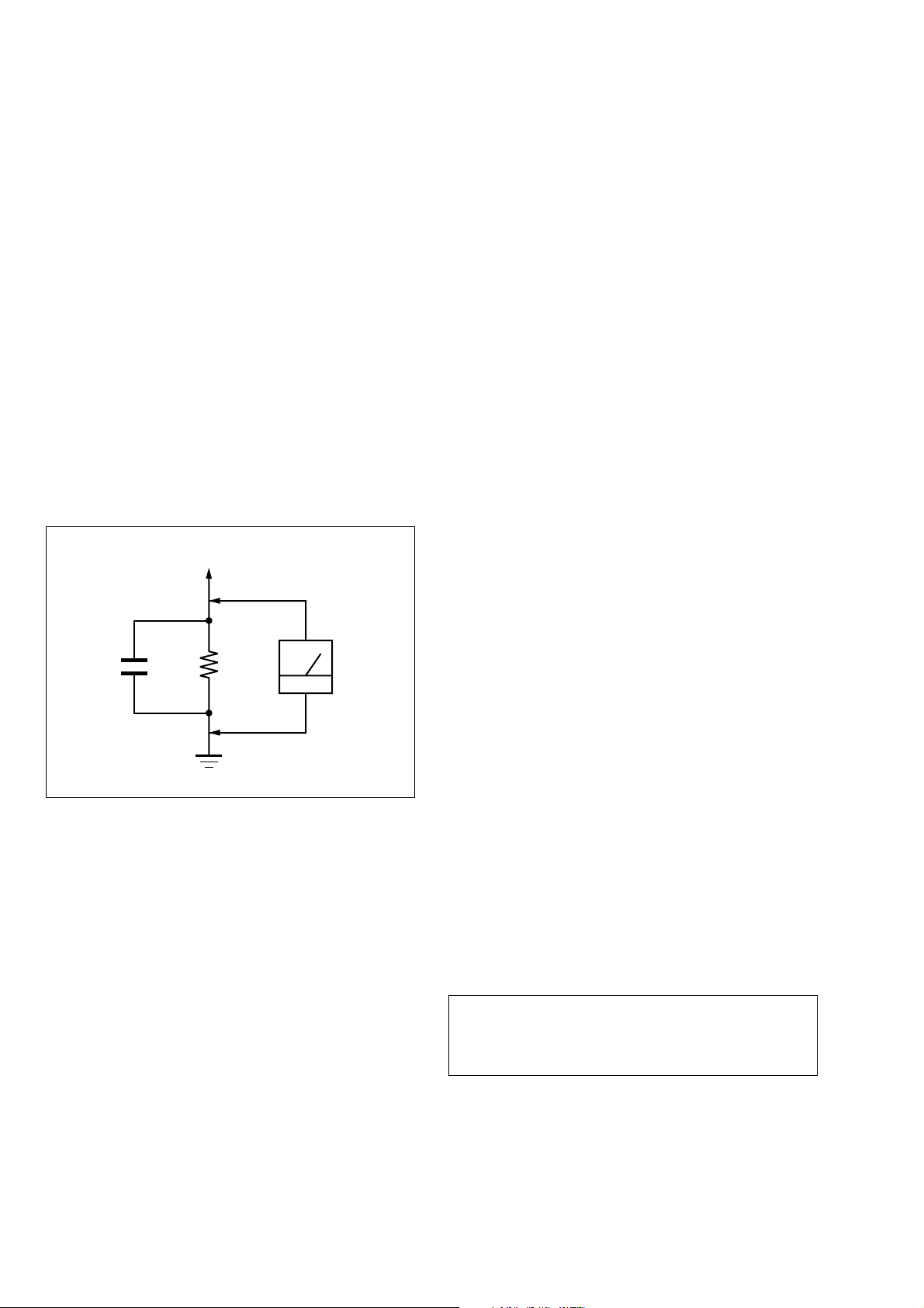
LEAKA GE TEST
The AC leakage from any exposed metal part to earth ground
and from all exposed metal parts to any e xposed metal part having
a return to chassis, must not exceed 0.5 mA (500 microamperes).
Leakage current can be measured by any one of three methods.
1. A commercial leakage tester, such as the Simpson 229 or RCA
WT-540A. F ollow the man ufacturers' instructions to use these
instruments.
2. A battery-operated AC milliammeter. The Data Precision 245
digital multimeter is suitable for this job.
3. Measuring the voltage drop across a resistor by means of a
VOM or battery-operated AC voltmeter. The “limit” indica-
tion is 0.75V, so analog meters must have an accurate low-
voltage scale. The Simpson 250 and Sanwa SH-63T r d are ex-
amples of a passive VOM that is suitable. Nearly all battery
operated digital multimeters that have a 2V AC range are suit-
able. (See Fig. A)
1.5 k
0.15 µF
Fig. A. Using an AC voltmeter to check AC leakage.
Ω
Earth Ground
AC
voltmeter
(0.75 V)
WARNING!!
WHEN SERVICING, DO NOT APPR OA CH THE LASER
EXIT WITH THE EYE TOO CLOSELY. IN CASE IT IS
NECESSARY TO CONFIRM LASER BEAM EMISSION,
BE SURE TO OBSERVE FROM A DISTANCE OF
MORE THAN 25 cm FROM THE SURFACE OF THE
OBJECTIVE LENS ON THE OPTICAL PICK-UP BLOCK.
CAUTION:
The use of optical instrument with this product will increase eye
hazard.
CAUTION
Use of controls or adjustments or performance of procedures
other than those specified herein may result in hazardous radiation exposure.
SAFETY-RELATED COMPONENT WARNING!!
COMPONENTS IDENTIFIED BY MARK 0 OR DOTTED
LINE WITH MARK 0 ON THE SCHEMATIC DIA GRAMS
AND IN THE PARTS LIST ARE CRITICAL TO SAFE
OPERATION. REPLACE THESE COMPONENTS WITH
SONY PARTS WHOSE PART NUMBERS APPEAR AS
SHOWN IN THIS MANUAL OR IN SUPPLEMENTS PUBLISHED BY SONY.
– 2 –
Page 3

TABLE OF CONTENTS
Section Title Page Section Title Page
Service Note ............................................................................ 4
1. GENERAL
Getting Started .............................................................. 1-1
Playing Discs................................................................. 1-4
Using Various Functions with the Control Menu........... 1-6
Settings and Adjustments ............................................. 1-10
2. DISASSEMBLY
2-1. Case Removal ............................................................... 2-1
2-2. Rear Panel Removal ..................................................... 2-1
2-3. Tray Cover Removal ...................................................... 2-1
2-4. Front Panel Removal..................................................... 2-1
2-5. Power Block Removal ................................................... 2-2
2-6. Mechanism Deck Removal ............................................ 2-2
2-7. Tray Removal................................................................. 2-2
2-8. Optical Pick-up Removal............................................... 2-2
2-9. Belt, MB-86 Board, Loading Motor (M001),
MS-48 Board Removal .................................................. 2-3
2-10. AI-022 Board Removal.................................................. 2-3
2-11. Internal Views ................................................................ 2-4
2-12. Circuit Boards Location................................................. 2-5
3. BLOCK DIAGRAMS
6. TEST MODE
6-1. General Description ...................................................... 6-1
6-2. Starting Test Mode ........................................................ 6-1
6-3. Syscon Diagnosis.......................................................... 6-1
6-4. Drive Auto Adjustment .................................................. 6-5
6-5. Drive Manual Operation ................................................ 6-7
6-6. Mecha Aging ................................................................. 6-9
6-7. Emergency History........................................................ 6-9
6-8. Version Information ....................................................... 6-1 0
6-9. Video Level Adjustment ................................................ 6-10
6-10. If Con Self Diagnostic Function .................................... 6-11
7. ELECTRICAL ADJUSTMENT
7-1. Power Supply Adjustment............................................. 7-1
1. Power Supply Check ..................................................... 7-1
7-2. Adjustment of Video System......................................... 7-2
1. Video Level Adjustment ................................................ 7-2
2. S-terminal Output Check............................................... 7-2
3. Checking Component Video Output B-Y ...................... 7-2
4. Checking Component Video Output R-Y ...................... 7-2
5. Checking Component Video Output Y .......................... 7-3
6. Checking S Video Output S-C....................................... 7-3
7-3. Adjustment Related Parts Arrangement ....................... 7-4
3-1. Overall Block Diagram................................................... 3-1
3-2. RF/Servo Block Diagram............................................... 3-3
3-3. Signal Processor Block Diagram .................................. 3-5
3-4. Video/Audio Block Diagram .......................................... 3-7
3-5. System Control Block Diagram ..................................... 3-9
3-6. Interface Control Block Diagram ................................... 3-11
3-7. Power Block Diagram .................................................... 3-13
4. PRINTED WIRING BOARDS AND SCHEMATIC
DIAGRAMS
4-1. Frame Schematic Diagram ............................................ 4-3
4-2. Printed Wiring Boards and Schematic Diagrams ......... 4-5
MS-48 Printed Wiring Board and
Schematic Diagram....................................................... 4-5
MB-86 Printed Wiring Board ......................................... 4-7
MB-86 (RF AMP, SERVO) Schematic Diagram ............ 4-11
MB-86 (ARP) Schematic Diagram ................................ 4-13
MB-86 (AV DECODER) Schematic Diagram................ 4-15
MB-86 (SDRAM) Schematic Diagram .......................... 4-17
MB-86 (DRIVE) Schematic Diagram ............................ 4-19
MB-86 (SERVO DSP) Schematic Diag ram................... 4-21
MB-86 (SYSTEM CONTROL)
Schematic Diagram....................................................... 4-23
MB-86 (MEMORY, CLOCK GENERATOR)
Schematic Diagram....................................................... 4-25
AI-022 Printed Wiring Board ......................................... 4-27
AI-022 (VIDEO BUFFER) Schematic Diagram ............. 4-29
AI-022 (D/A CONVERTER, DSP)
Schematic Diagram....................................................... 4-31
AI-022 (POWER SUPPLY) Schematic Diagram ........... 4-33
AI-022 (IF CON) Schematic Diagram ........................... 4-35
FR-177, FL-118 Printed Wiring Boards and
Schematic Diagrams ..................................................... 4-37
HS16S9U Printed Wiring Board.................................... 4-39
HS16S9U Schematic Diagram...................................... 4-41
8. REPAIR PARTS LIST
8-1. Exploded Views ............................................................. 8-1
8-1-1. Case Assembly ........................................................ 8-1
8-1-2. Chassis Assembly.................................................... 8-2
8-1-3. Mechanism Deck Section ........................................ 8-3
8-2. Electrical Parts List ....................................................... 8-4
5. IC PIN FUNCTION DESCRIPTION
5-1. System Control Pin Function
(MB-86 Board IC102) .................................................... 5-1
– 3 –
Page 4
SERVICE NOTE
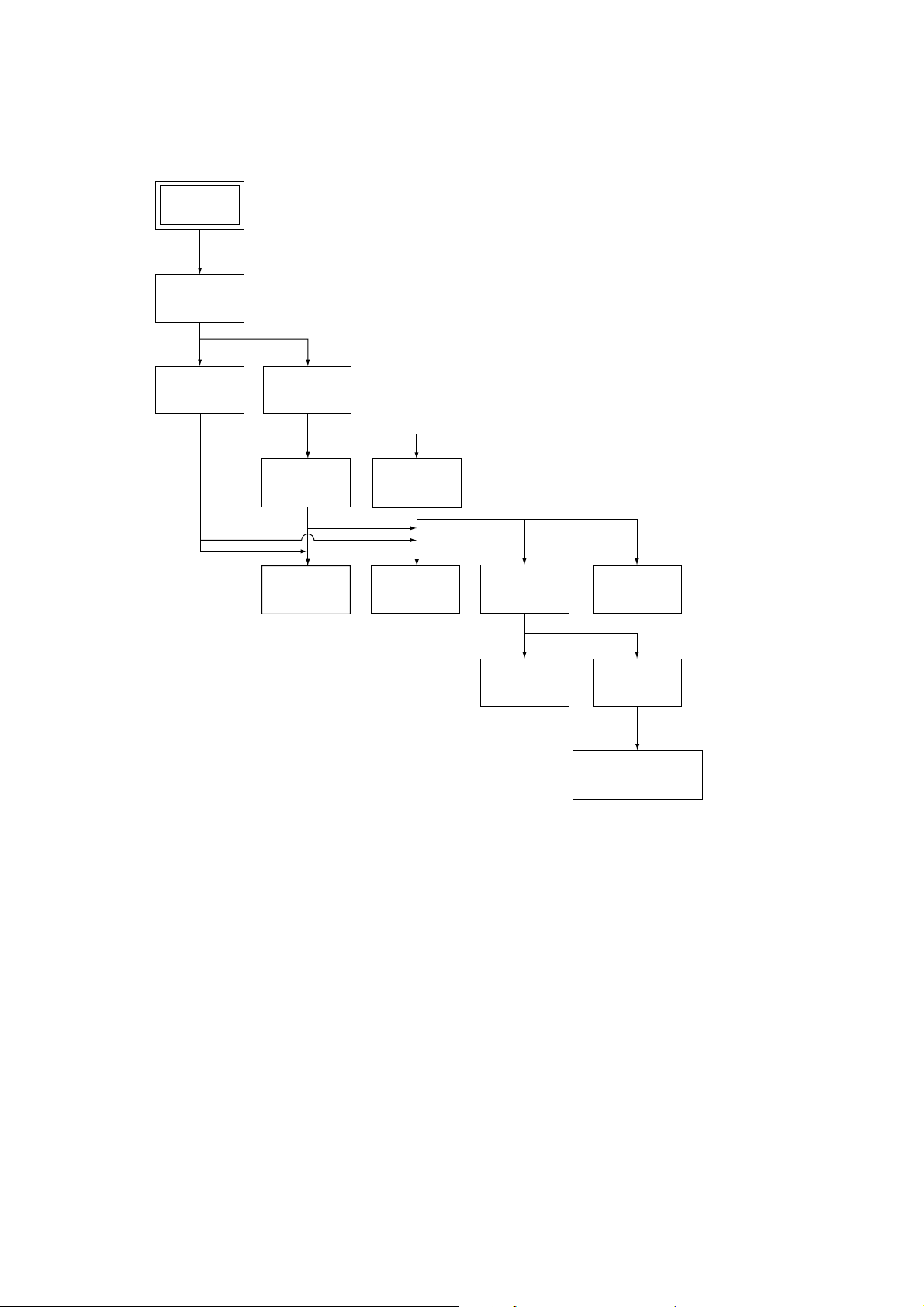
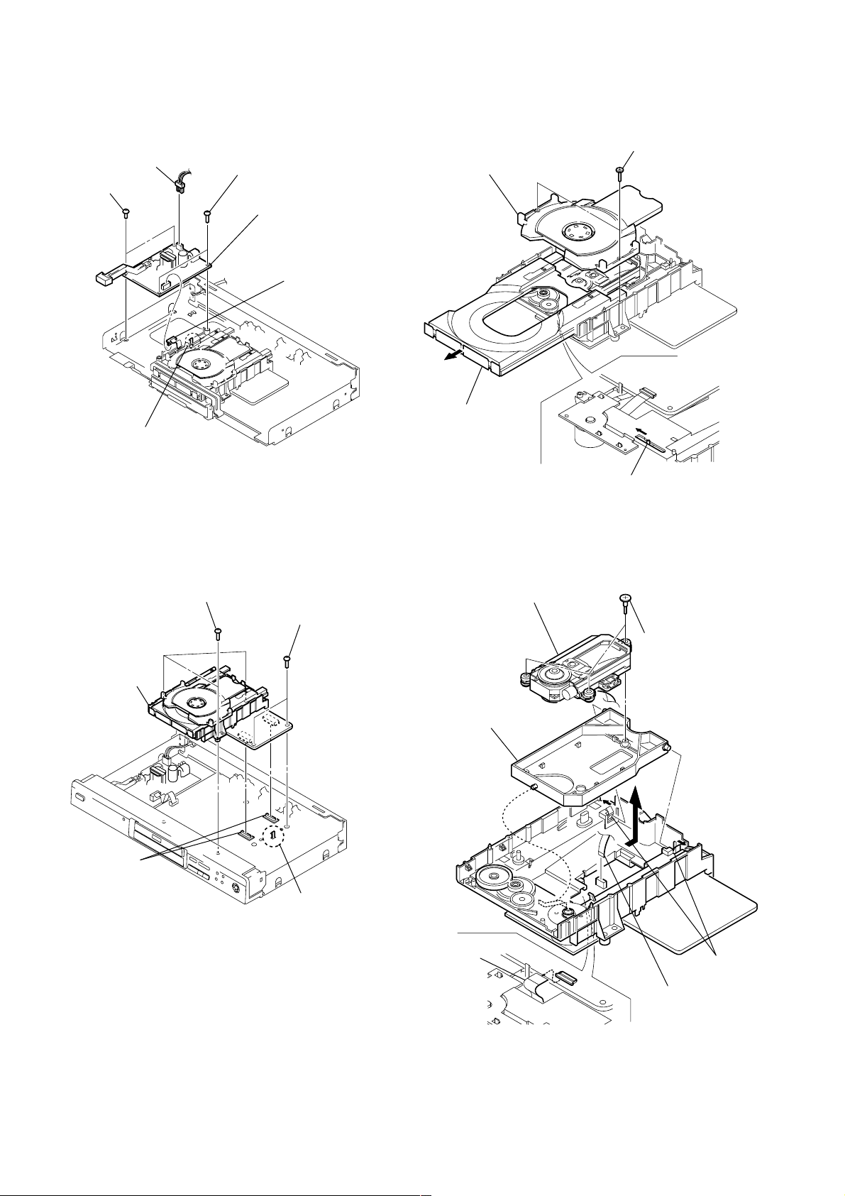
1. DISASSEMBLY
• This set can be disassembled in the order shown below.
Set
Case
(Page 2-1)
Rear Panel
(Page 2-1)
Tray Cover
(Page 2-1)
Front Panel
(Page 2-1)
Power
Block
(Page 2-2)
Mechanism
Deck
(Page 2-2)
AI-022 Board
(Page 2-3)
Tray
(Page 2-2)
Optical Pick-up
(Page 2-2)
MB-86 Board
(Page 2-3)
Belt
(Page 2-3)
Loading Motor (M001),
MS-48 Board
(Page 2-3)
– 4 –
Page 5
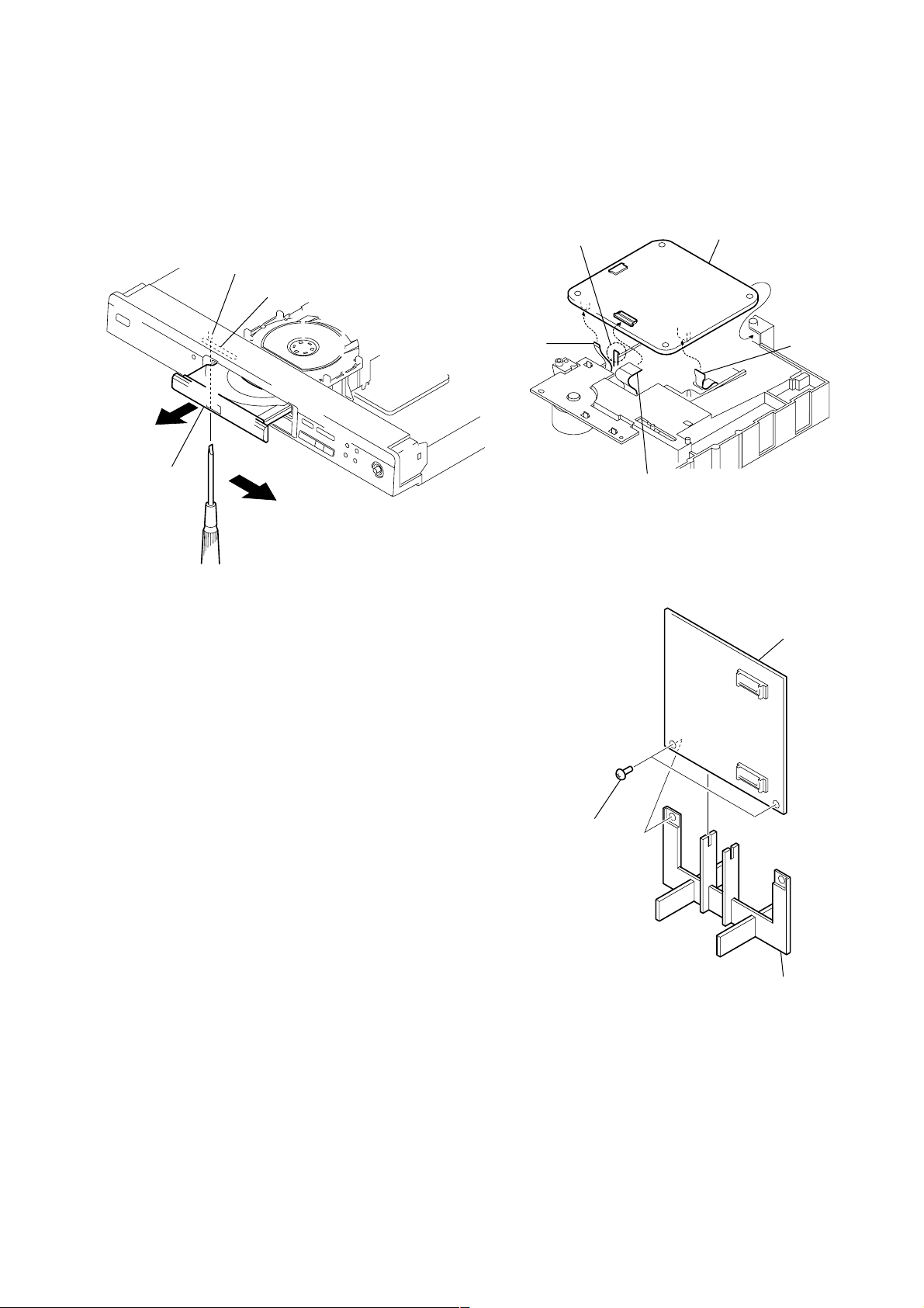
2. DISC REMOVAL PROCEDURE
(at POWER OFF)
1) Insert a tapering driver into the aperture of the unit bottom,
and move the lever of chuck cam in the direction of the arrow
A. (See Fig. 1)
2) Draw out the tray in the direction of the arrow B, and remove
a disc. (See Fig. 1)
Lever of chuck cam
Aperture
B
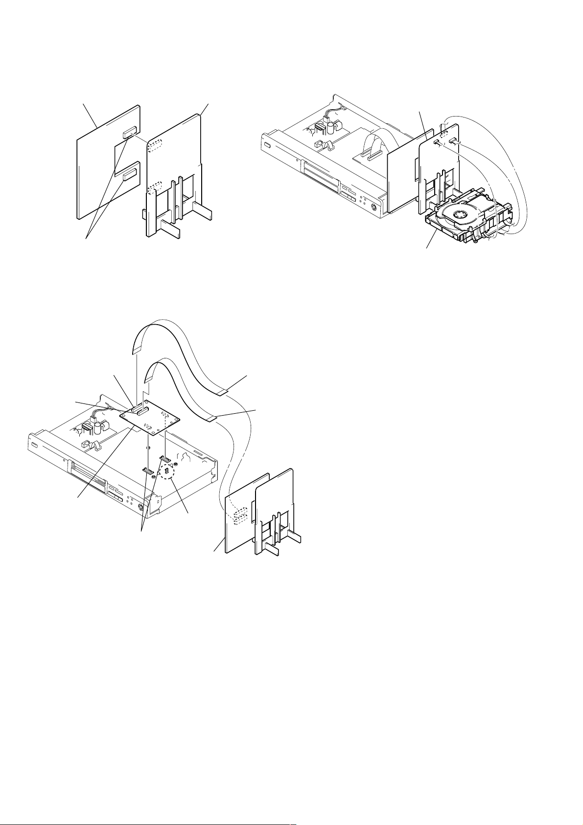
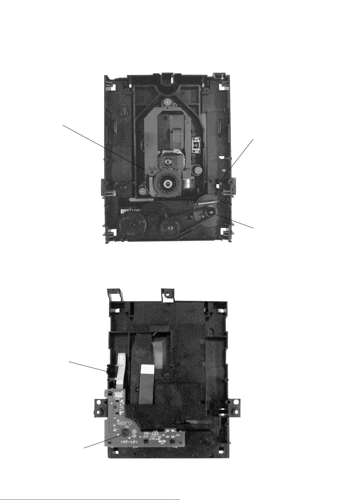
3. HOW TO SERVICE MB-86 BOARD
1) Remove the case from the set. (Refer to 2-1)
2) Remove the mechanism deck. (Refer to 2-2)
3) Remove the MB-86 board. (Refer to 2-3)
4) Set the CK-MD board as shown in Fig. 2.
4 Claw
1 Flexible board
(CN005)
5 CK-MD board
2 Flexible board
(CN001)
Tray
A
Fig. 1
3 Flexible board
(CN002)
Fig. 2
5) Set the MB-86 board as shown in Fig. 3.
1 MB-86 board
3 Two ground point
screws
– 5 –
2 Stand
Fig. 3
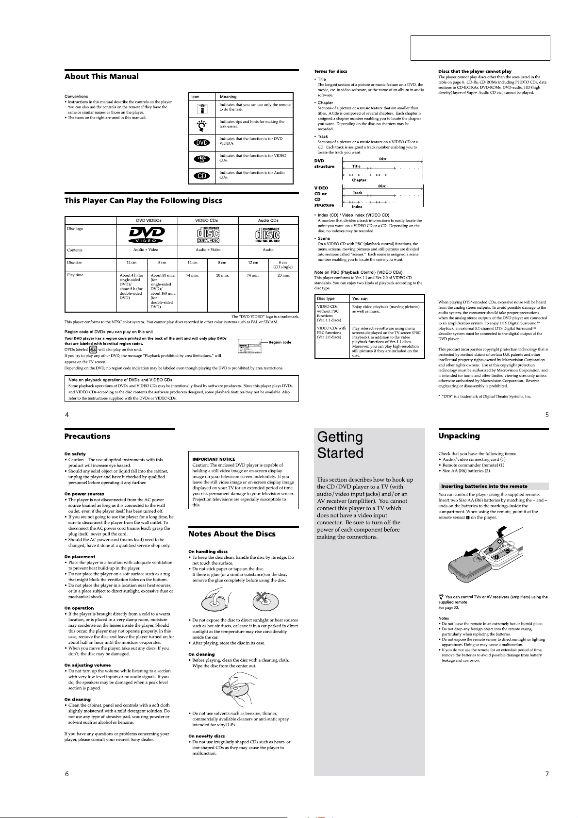
Page 6
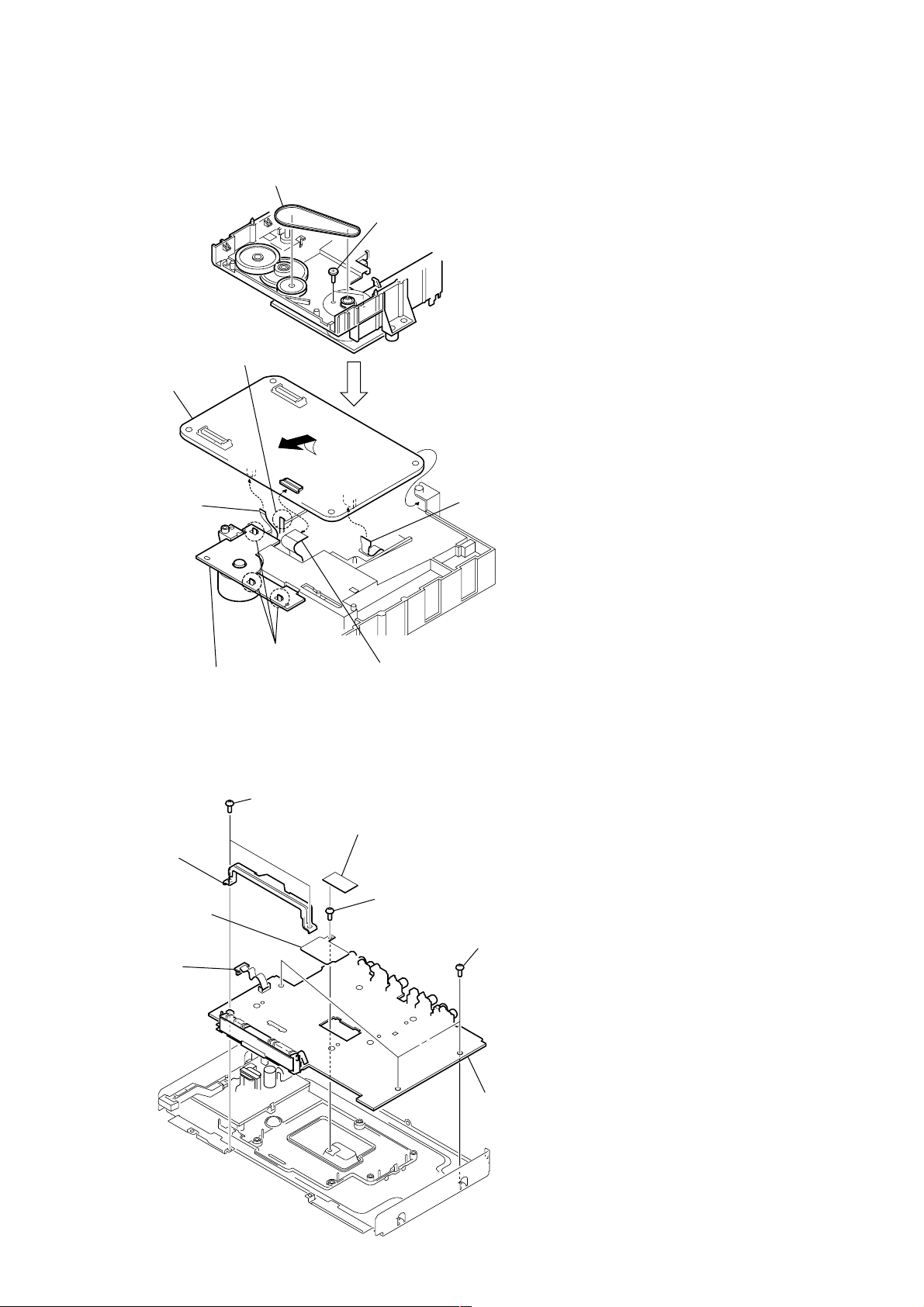
6) Set the CK-MB board as shown in Fig. 4.
8) Set the mechanism deck as shown in Fig. 6.
3 CK-MB board
2 Two connectors
(CN101, 102)
Fig. 4
7) Set the CK-AI board as shown in Fig. 5.
5 Connector
(CN103)
4 Connector
(CN104)
1 MB-86 board
MB-86 board
Mechanism deck
Fig. 6
7 Flexible board
(CN104)
6 Flexible board
(CN103)
3 CK-AI board
2 Claw
1 Two connectors
(CN101, 102)
CK-MB board
Fig. 5
– 6 –
Page 7
SECTION 1
GENERAL
DVP-S350
This section is extr acted from instruction manual (3-062-657-11).
1-1
Page 8

1-2
Page 9
1-3
Page 10
1-4
Page 11
1-5
Page 12
1-6
Page 13
1-7
Page 14
1-8
Page 15
1-9
Page 16
1-10
Page 17
1-11
Page 18
1-12
Page 19
1-13
Page 20
1-14 E
1-14
Page 21

SECTION 2
7 Claw
6 Claw
1 Flat cable
(CN405)
8 Front panel
5 Two claws
2 Two connectors
(CN412, 413)
3 Screws (B3)
4 Harness
DISASSEMBLY
Note: Follow the disassembly procedure in the numerical order given.
2-1. CASE REMOVAL 2-3. TRAY COVER REMOVAL
DVP-S350
1 Two screws
(Case 3 TP 2)
4 Case
3 Screw
(Case 3 TP 2)
2 Two screws
(Case 3 TP 2)
B
2 Pull the tray in the
direction of arrow B.
3 Two claws
4 Tray cover
A
1 Insert a tapering driver
into the aperture of the unit
bottom, and move the lever
of chuck cam in the direction
of arrow A.
2-2. REAR PANEL REMOVAL 2-4. FRONT PANEL REMOVAL
6 Rear panel
1 Connector
(CN101)
5 Claw
2 Five screws (B3)
3 Five screws (B3)
4 Claw
2-1
Page 22
2-5. POWER BLOCK REMOVAL 2-7. TRAY REMOVAL
1 Connector
(CN101)
3 Two screws (B3)
5 Claw
4 Two ground point
screws
6 Power block
2 Connector
(CN201)
2 Chuck ass’y
B
4 Remove the tray
in the direction of
arrow B.
1 Two screws
(BTP2.6 × 12)
A
3 Move the lever of chuck cam
in the direction of arrow A.
2-6. MECHANISM DECK REMOVAL 2-8. OPTICAL PICK-UP REMOVAL
2 Three ground point screws
1 Two ground point screws
5 Mechanism deck
4 Remove the base
3 Two connectors
(CN101, 201)
4 Claw
6 Optical pick-up
5 Three step
screws
unit holder in the
direction of arrow A.
A
1 Flexible board
(CN202)
3 Two claws
2-2
2 Flexible board
(CN201)
Page 23
2-9. BELT, MB-86 BOARD, LOADING MOTOR (M001),
MS-48 BOARD REMOVAL
1 Belt
2 Two screws
(B2.6 × 4)
4 Claw
7 MB-86 board
6 Flexible board
(CN401)
8 Three claws
9 Loading motor (M001),
MS-48 board
2-10. AI-022 BOARD REMOVAL
2 Two screws (B3)
3 Multi pillar
7 Shield (BU)
1 Connector
(CN201)
5 Flexible board
(CN201)
3 Flexible board
(CN202)
5 Cushion (D)
6 Screw (B3)
4 Three screws
(B3)
8 AI-022 board
2-3
Page 24
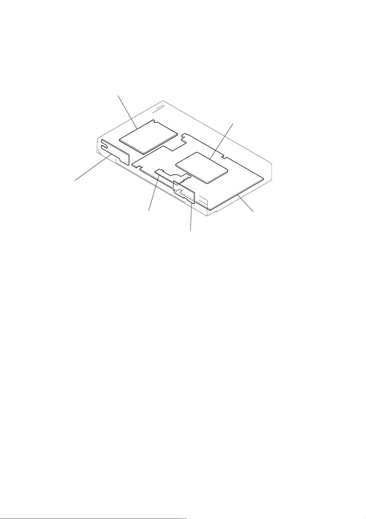
2-11. INTERNAL VIEWS
Optical pick-up
(KHM-220AAA)
A-6062-397-A
Lever switch
1-771-562-11
Flexible flat cable
1-792-457-11
DC motor (loading)
1-541-632-11
DC motor (loading)
1-541-632-11
2-4
Page 25
2-12. CIRCUIT BOARDS LOCATION
Power Block
(HS16S9U)
(SWITCHING REGULATOR)
FL-118
(IR/SURROUND SWITCH)
MB-86
(SIGNAL PROCESS, SERVO)
MS-48
(LOADING)
AI-022
(AUDIO, VIDEO BUFFER)
FR-177
(FUNCTION SWITCH)
2-5
2-5 E
Page 26
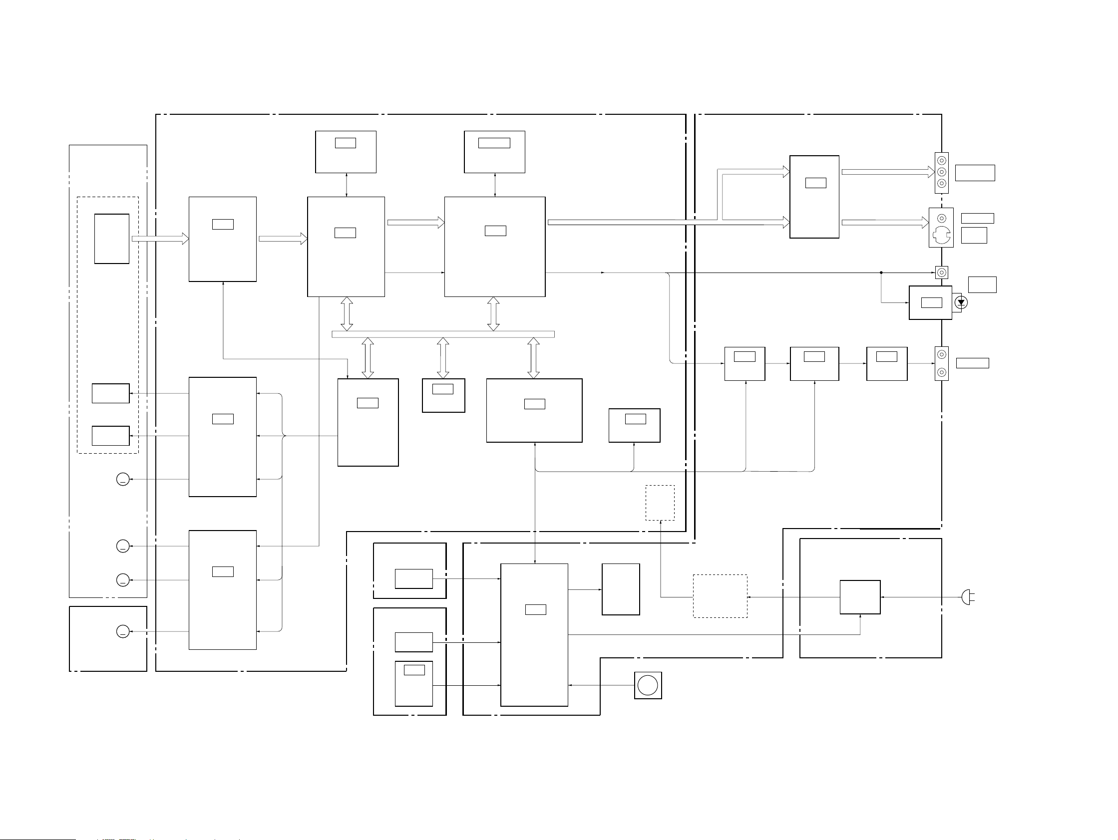
3-1. OVERALL BLOCK DIAGRAM
DVP-S350
SECTION 3
BLOCK DIAGRAMS
BASE UNIT
KHM-220AAA/J1N2
OPTICAL DEVICE
DVD/CD
PD IC
FOCUS
COIL
TRACKING
COIL
TILT
MOTOR
MB-86 BOARD
(SEE PAGE 4-11 to 4-26)
RF
DVD/CD RF AMP
FOCUS/TRACKING
TILT MOTOR
IC201
IC401
COIL
DRIVE,
DRIVE
DVD/CD RF
IC303
16M DRAM
IC302
ARP
IC404
SERVO
DSP
SD0 – 7
CD DOUT, CD DATA,
CD BCK, CD LRCK
PARALLEL BUS
IC106
OTP
IC504, 505
16M SDRAM
IC502
AV
DECODER
IC102
SYSTEM
CONTROL
SPDIF, ACH12,
ACH34, ACH56,
BCK, LRCK
SERIAL BUS
IC101
EEPROM
AI-022 BOARD
(SEE PAGE 4-29 to 4-36)
VIDEO Y,
VIDEO B – Y,
VIDEO R –Y
VIDEO V,
VIDEO Y,
VIDEO C
SPDIF
IC205
VES
DSP
IC101
VIDEO
BUFFER
IC201
AUDIO
D/A CONVERTER
IC208
AMP
LPF
IC306
COMPONENT
VIDEO OUT
VIDEO OUT
S VIDEO
OUT
DIGITAL
OUT
AUDIO OUT
MM
+10V
+5V
+1.8V
+3.3V
SPINDLE
MOTOR
SLED
MOTOR
M001
LOADING
MOTOR
MS-48 BOARD
(SEE PAGE 4-6)
05
MM
MM
IC402
SPINDLE/SLED/
LOADING
MOTOR DRIVE
MM
FR-177 BOARD
(SEE PAGE 4-38)
SWITCH
FL-118 BOARD
(SEE PAGE 4-38)
SWITCH
IC401
REMOTE
COMMANDER
RECEIVER
IC404
IF CON
P CON
ND401
ENTER
CURSOR KEY
EVER +3.8V
SW +3.3V
EVER +5.6V
SW +10V
SW –10V
HS16S9U BOARD (SEE PAGE 4-41)
SWITCHING
REGULATOR
AC IN
3-1 3-2
Page 27

DVP-S350
3-2. RF/SERVO BLOCK DIAGRAM
BASE UNIT
KHM-220AAA/J1N2
LD MODULE
DVD/CD
PD IC
DVD/CD
IC201 1 (DVD play)
200 mV/DIV 100 ns/DIV
536 mVp-p
MB-86 BOARD (1/5)
(SEE PAGE 4-11, 19, 21)
CN201
RF
7
9
A – D
10
16
17
8
E – H
11
15
18
VC
13
PD
4
LD
2
VR
5
IC201 1 (CD play)
500 mV/DIV 500 ns/DIV
880 mVp-p
1
9
ı
12
5
ı
8
13
ı
16
17
19
Q201
LD DRIVE
20
IC201 tf (DVD play)
500 mV/DIV 100 ns/DIV
IC201
DVD/CD RF AMP
DIGITAL SERVO
RF IP
A – D
A2 – D2
E – H
VC
PD
LD
LDON
25
1.5 Vp-p
SIGO
FE
TE
PI
MIRR
TZC
SCLK
SWD
SRD
SDEN
FDCHG
DFT
HOLD2
IC201 tf (CD play)
500 mV/DIV 500 ns/DIV
54
33VCI
40
39
29
26
32
43
ı
46
27
31
42
IC201 wl (DVD play)
200 mV/DIV 500 ms/DIV
1.5 Vp-p
IC201 r; (DVD play)
100 mV/DIV 50 ms/DIV
IC201 el (DVD play)
500 mV/DIV 50 ms/DIV
FE
TE
PI
SSDFCT
SSDFCTI
IC201 wl (CD play)
200 mV/DIV 20 ms/DIV
180 mVp-p
1.3 Vp-p
22
23
21
27
26
45
ı
48
41
34
ADC1
ADC0
ADC2
MIRR
TZC
GIO5 – 8
GIO11
DFCTI
IC201 r; (CD play)
500 mV/DIV 50 ms/DIV
860 mVp-p
IC201 el (CD play)
500 mV/DIV 200 ms/DIV
1.7 Vp-p
IC404 wd (DVD play)
500 mV/DIV 50 ms/DIV
1.4 Vp-p
IC404 wd (CD play)
500 mV/DIV 200 mV/DIV
1.7 Vp-p
IC404 ws (DVD play)
100 mV/DIV 50 ms/DIV
180 mVp-p
ADC4
19
ADC5
18
FGREF
31
9 8 12VRTA
VRBA
13
IC404 ws (CD play)
500 mV/DIV 50 ms/DIV
14
1
860 mVp-p
IC403 (2/2)
REFERENCE
VOLTAGE
GENERATOR
RF+
(DVD/CD) RF
MDS0
MDP0
LOCK
+3.3V
SIGNAL PROCESSOR
(SEE PAGE 3-5)
FOCUS
COIL
TRACKING
COIL
TILT
MM
MOTOR
INLIMIT
SENSOR
SPINDLE
MM
MOTOR
SLED
MM
MOTOR
MS-48 BOARD (SEE PAGE 4-6)
M001
LOADING
MM
MOTOR
CHUCK
S001
SENSOR
FCS
TRK
TIA, TIB
INLIM
SPM
SLA, SLB
1
2
3
5
PWM2
IC404
SERVO DSP
GIO0
72 73
PWM0, 1
GIO13
GIO14
HA 0, 1
HD 0 – 7
HINT
HCS
HWR
HRD
CLKIN
80
81
82
ı
84
86
ı
90
76
77
78
79
95
RS
68
HA 0, 1
HD 8 – 15
HA 0, 1
HD 8 – 15
SDSPINT
XSDSPCS
WRH
RD
27MSDP
XRST
XDRVMUTE
OCSW1
OCSW2
SYSTEM CONTROL
(SEE PAGE 3-9, 10)
5
6
448 mVp-p
IC403 (1/2)
TILT A1, B1
TILT MUTE1
SLDA1, B1
SPDL1
SPCNT1
LDMD1
LDFREE
7 17
1
3
5
7
53
54
49
32
ADC6
PDM 2, 3
PDM 0, 1
ADC3
GIO1, 2
GIO4
FGIN
71 55 39 38
Q203
IC401
FOCUS
COIL
DRIVE
TRACKING
COIL
DRIVE
TILT
MOTOR
DRIVE
SPINDLE
MOTOR
DRIVE
SLED
MOTOR
DRIVE
LOADING
MOTOR
DRIVE
14
15
20
28
29
12
13
11 20
22
25
30
15
29
22
25
20
30
12
28
IC402
2
3
4
5
32
ı
35
2
3
32
ı
35
4
5
19
20
21
22
CN202
10
ı
13
2
8
9
4
ı
7
CN401CN001
5
6
2
4
592 mVp-p
TRAY
S002
05
SENSOR
3
4
CKSW1
3-3 3-4
Page 28

3-3. SIGNAL PROCESSOR BLOCK DIAGRAM
MB-86 BOARD (2/5)
(SEE PAGE 4-13 to 4-18)
IC303
16M DRAM
DVP-S350
IC504, 505
16M SDRAM
RF/SERVO
(SEE PAGE 3-4)
SYSTEM CONTROL
(SEE PAGE 3-9, 10)
IC302 qj (DVD play)
500 mV/DIV 100 ns/DIV
RF+
(DVD/CD) RF
MDSO
MDPO
LOCK
ARINT
XARPCS
ARPWT
ARPRST
33MARP
WRH
RD
HA 0 – 21
1.6 Vp-p
HA 0 – 21
CS, WE,
CAS, RAS
MA 0 – 9
136 – 139
141 – 144
146 147
IC302 ql (CD play)
17
RFIN1
19
RFIN2
49
MDSO
52
MDPO
58
LOCK
83
XINT
84
XCS
86
XWAT
87
XRST
121
MCKI
123
SCKI
60
XWR
61
XRD
500 mV/DIV 200 ns/DIV
MD 0 – 15
154 – 157
159 – 162
164 – 167
169 – 172
1.6 Vp-p
IC302
ARP
UCAS, LCAS
WE, RAS, OE,
148
150 – 152
SD 0 – 7
A 0 – 7 HA 0 – 7
97
98
SDI 0 – 7 DTI 0 – 7
100
ı
105
ı
ı
ı
ı
ı
HD 8 – 15
SDCK, XSHD,
XSRQ, XSAK, SDEF
CD DATA, CD BCK,
CD LRCK, CD DOUT
HD 0 – 15D 0 – 7
91
93
96
107
110
73
76
79
82
63
68
70
71
RD
WRH
31
ı
34
36
ı
39
41
43
ı
46
22
23
25
26
192 193
195 – 198
200 – 203
205 – 208
210 – 213
215 – 218
2 – 5
7 – 10
232 – 235
237 – 240
HCSB
220
221
HRWB
SDAD 0 – 11
124 125 127 128
130 131 133 134
136 137 139 140
IC502 i;
1.2 Vp-p (H)
HAD 0 – 21HA 0 – 21
HD 0 – 15
SDDT 0 – 15
157 – 160 162 – 165
167 168 170 171
173 174 176 177
IC502 yd
720 mVp-p (H)
IC502 yh
728 mVp-p (H)
IC502 uf
1.1 Vp-p (H)
IC502 uj
520 mVp-p (H)
IC502
AV DECODER
CLK, CKE,
DQML, DQMU,
143 144 146
147 149 151
152 154 155
G OUT/Y
R OUT/B-Y
B OUT/R-Y
COMPOUT
Y OUT
C OUT
VREFI
ACH12
ACH34
ACH56
LRCKO
BCKO
IC502 yl
1.0 Vp-p (H)
69
63
66
80
74
77
84
14
15
16
18
19
20
DO
VIDEO Y
VIDEO B-Y
VIDEO R-Y
VIDEO V
VIDEO Y
VIDEO C
RV501
VIDEO
LEVEL
ADJ
Y/G
CB/R
CR/B
VIDEO V
VIDEO Y
VIDEO C
6CH FRONT
6CH REAR
6CH C/SW
LRCK
BCK
SPDIF
VIDEO/AUDIO
(SEE PAGE 3-7)
HD 0 – 15
XAVDCS2
XAVDCS3
512FSAVD
33MAVD
27MAVD
XRST
XV3RST
AVINT
AVWT
DACK0
DREQ0
DACK1
DREQ1
05
HD 0 – 15
190
191
12
29
180
182
231
HAD23
HAD22
ACLK
CRPCLKI
CLKI
SCLKIN
RSTB
223 224 226 – 229
TDO
TCK
TMS
TRST
118TDI
119
120
121
122
LAND
(FOR J TAG)
3-5 3-6
Page 29

DVP-S350
3-4. VIDEO/AUDIO BLOCK DIAGRAM
MB-86 BOARD (3/5)
(SEE PAGE 4-15)
SIGNAL
PROCESSOR
(SEE PAGE 3-6)
6CH FRONT
CB/R
CR/B
VIDEO V
VIDEO Y
VIDEO C
SPDIF
6CH REAR
6CH C/SW
BCK
LRCK
Y/G
CN501
CN701 (1/2)
30
25
29
10
18
14
26
34
14
16
18
20
Y/G
CB/R
CR/B
VIDEO V
VIDEO Y
VIDEO C
WIDE
SPDIF
6CH FRONT
6CH REAR
6CH C/SW
BCK
AI-022 BOARD (1/2)
(SEE PAGE 4-29 to 4-32)
CN101 (1/2)
5
10
6
25
17
21
9
INTERFACE
CONTROL
(SEE PAGE 3-11)
CN201 (1/2)
1
21
19
17
15
VMUTE
A MUTE
IC101 wg
IC101
VIDEO BUFFER
Y/G
CB/R
CR/B
VIDEO V
VIDEO Y
VIDEO C
Q106, 107
IC205
VES DSP
6
SDIO
7
SDI1
8
SDI2
9
BCKI
5
LRCKI
WIDE
SWITCH
SDO0
11
14
17
13
20
1
7
4
3
30
Y IN
CB IN
CR IN
MUTE
MUTE
VIDEO IN
Y IN
C IN
MUTE
MUTE
37
IC101 eg
2.4 Vp-p (H)
IC101 ea
2.1 Vp-p (H)
IC101 ed
520 mVp-p (H)
3
4
5
D/A CONVERTER
SDATA
SCLK
LRCK
Y OUT
CB OUT
CR OUT
VIDEO
OUT
Y OUT
C OUT
IC201
AUDIO
25
23
21
35
31
33
AOUT B+
AOUT B–
AOUT A+
AOUT A–
15
14
18
19
1.0 Vp-p (H)
IC101 wa
728 mVp-p (H)
IC101 wd
720 mVp-p (H)
IC208
AMP/LPF
5
6
3
2
J103
7
1
J101
J102
Y
C
Y
PB/B-Y
PR/R-Y
VIDEO OUT
S VIDEO
OUT
COMPONENT
VIDEO OUT
Q313
MUTE
Q203
MUTE
Q204
J303
COAXIAL
1
D IN
J201
OPTICAL
L
AUDIO OUT
R
IC306
DIGITAL
OUT
SYSTEM
CONTROL
(SEE PAGE 3-10)
05
WIDE
6CH/VES CS
XRST
512FS2CH/VES
SI1
SO1
SC1
AURST
2CH CS
MA MUTE
6CH/VES CS
3
6CH REAR/XRST
9
BCK
4
LRCK
6
512FS2CH/VES
10
22
26
SCK1
24
AURST
1
2CH CS
28
MA MUTE
30
6
MCLK
SDA
SCL
RST
9 8 1 10
CS
AMUTE C
20
MUTE DRIVE
Q205
SI1
SO1
3
MCLK
32
26
31
29
25
13
9
11
34
7
5
11 XCS
48
XRST
SCK
SI
SO
1413
17
3-7 3-8
MUTE DRIVE
Q206, 207
Page 30

3-5. SYSTEM CONTROL BLOCK DIAGRAM
MB-86 BOARD (4/5)
(SEE PAGE 4-23 to 4-26)
DVP-S350
IC106
OTP
SIGNAL PROCESSOR
(SEE PAGE 3-5)
RF/SERVO
(SEE PAGE 3-4)
SIGNAL PROCESSOR
(SEE PAGE 3-5)
HA 0 – 21
HD 0 – 15
HA 0, 1
HD 8 – 15
XDRVMUTE
SDSPINT
XSDSPCS
CKSW1
OCSW1
OCSW2
WRH
WRH
ARPRST
ARINT
XARPCS
ARPWT
AVWT
DREQ0
DACK0
DREQ1
DACK1
XAVDCS2
XAVDCS3
AVINT
HA 0 – 21
HD 0 – 15
IC105 8,9
HD0 – 15 HD0 – 15
85 – 100
INT3
ECS
EWC
SI0
SO0
SC0
IFCS
INT4
FRRST IN
WIDE
AURST
DACCS1
DACCS0
MAMUTE
SC1
SO1
SI1
44.1/48k
28
49
48
33
35
36
45
29
74
63
51
60
59
62
39
38
37
16XRST
DVD: 4.3 Vp-p (29.5 MHz)
CD: 4.3 Vp-p (22.58 MHz)
61
1
3
8
IC105 qh
IC1054
R/B
CS
X102
27MHz
IC101
EEPROM
SKWCDI
4
5
6
23
8
9
DO
44.1/48k
IN
OUT
SI0
SO0
SC0
XIFCS
IFBSY
XFRRST
IC103
4
RESET
IC105
PLL
512FS2
15
16
512FS1
27M2
12
33M
27M3
24
IC105 wf
B+
5
(3.3V)
IC105 qg
DVD: 3.4 Vp-p (29.5 MHz)
CD: 3.4 Vp-p (22.58 MHz)
4
WIDE
AURST
6CH/VES CS
2CH CS
MA MUTE
SC1
SO1
SI1
512FS2CH/VES
XRST
XV3RST
XRST
512FSAVD
27MAVD
33MAVD
33MARP
XRST
27MSDP
IC105 qs
INTERFACE
CONTROL
(SEE PAGE 3-11)
VIDEO/AUDIO
(SEE PAGE 3-7)
SIGNAL PROCESSOR
(SEE PAGE 3-5)
RF/SERVO
(SEE PAGE 3-4)
HA 0, 1
HD 8 – 15
23
32
18
56
57
58
RD
RD
82
83
22
26
69
79
43
44
46
47
67
68
25
DRV MUTE
INT7
CS6
CKSW1
OCSW1
OCSW2
RD
WRH
ARPRST
INT1
CS4X
XWAIT
DREQ0
DACK0
DREQ1
DACK1
CS2X
CS3X
INTO
65
1 – 5 102 – 109 111 – 118 120
CSOX
IC102 tf
2.4 Vp-p (12.5 MHz)
X1
53 54
HA0 – 21 HA1 – 21
IC102
SYSTEM
CONTROL
X0
X101
12.5MHz
2.5 Vp-p (27 MHz)
5.2 Vp-p (27 MHz)
05
4.9 Vp-p (27.2 MHz)
4.9 Vp-p (33.8688 MHz)
3-9 3-10
Page 31

DVP-S350
3-6. INTERFACE CONTROL BLOCK DIAGRAM
MB-86 BOARD (5/5)
(SEE PAGE 4-15)
SYSTEM CONTROL
(SEE PAGE 3-10)
SC0
SI0
SO0
IFBSY
XIFCS
XFRRST
CN701(2/2)
AI-022 BOARD (2/2)
(SEE PAGE 4-33 to 4-36)
CN413 CN414
9
IR
CN201 (2/2)
SC0
SI0
SO0
IFBSY
XIFCS
XFRRST
2
6
4
10
8
12
POWER
(SEE PAGE 3-14)
VIDEO/AUDIO
(SEE PAGE 3-7)
P DET
P CONT
A MUTE
VMUTE
33
29
31
25
27
23
SC0
SI0
SO0
XIFBUSY
XIFCS
XFRRST
70
71
72
69
76
21
66
11
12
7
SC
SO
SI
BUSY
CS
FRRST
P DET
P CONT
AMUTE
VMUTE
IC404
IF CON
V3D/VES
AN7
AN4
AN3
62
79
CN412 CN411
2
3
SIRCS
3
LED V3D/VES
4
V3D/VES
5
AN4
5
AN3
4 4
FL-118 BOARD
(SEE PAGE 4-38)
3
4
5
FR-177 BOARD
(SEE PAGE 4-38)
5
IC401
REMOTE
1
COMMANDER
RECEIVER
D413
VES
S403
VES
S413 S410
TITLE DVD MENU
S414 S411 S408 S405
S407
NEXT
DISPLAY RETURN
S418
PREV
PLAY
4
PLAY
5
O/C
ND401
FLUORESCENT
INDICATOR TUBE
41 – 585 – 16
31
ı
SEG 1 – 18
48
49
ı
DIG 1 – 12
60
05
IC404 qg
3.2 Vp-p (2 MHz)
X1 X0
14
15
X401
2MHz
COMINT
AN5
RST
22
1
310
V OUT
IC403
RESET
3
OPEN/CLOSE
2
3
S415
2
S417
OPEN/CLOSE
LEFT
DOWN
ENTER
UP
RIGHT
CN405
2
1
3
4
6
CURSOR KEY
ENTER
3-11 3-12
Page 32

3-7. POWER BLOCK DIAGRAM
DVP-S350
AC IN
HS16S9U BOARD
(SEE PAGE 4-41)
SW101
F101
1
•
2
05
CN101
EVER +3.3V
LINE
FILTER
D101
Q101, 102
SWITCH
T101
PC101
PHOTO
COUPLER
P611
Q611
Q211
P612
Q312, 711
SWITCH
Q511
CN201
1
4
2
3
7
8
12
11
13
EVER +3.8V
EVER +5.6V
SW +3.3V
SW +3.3V
SW +10V
SW +10V
P CON
SW –10V
P DET
+10V
+5V
+1.8V
+3.3V
AI-022 BOARD
CN401
1
4
2
3
7
8
12
11
13
CN101
20
22
13
14
2
4
26
28
(SEE PAGE 4-29 to 4-36)
EVER +3.3V
IC407
+3.3V REG
IC406
+5V REG
PS402
PS401
IC102
+1.8V REG
SW +5V
SW +3.3V
EVER +3.3V
SW +3.3V
+10V
–10V
SW +5V
IC403
IC205 IC201
+5V
INTERFACE
CONTROL
(SEE PAGE 3-11)
–5V
P CONT
P DET
IC206
+5V REG
IC307
+8V REG
Q311
–8V REG
IC103
–5V REG
IC208
IC101
IC306
PCHK
Q401, 402
T401
DC/DC
CONVERTER
VEE
F1
F2
IC404
ND401
Q908, 909
LED DRIVE
CN413
EVER +5V
1 1
STANDBY LED
6 6
POWER LED
FL-118 BOARD
(SEE PAGE 4-38)
CN414
(ON/STANDBY)
77
IC401
D925
+3.3V
+1.8V
+5V
+10V
MB-86 BOARD
CN501
7
9
31
33
21
22
13
15
(SEE PAGE 4-11 to 4-26)
+5V
IC301
REG
IC503
REG
IC401
IC402
IC504
IC505
+3.3V
+1.8V
IC506
REG
+5V
IC101
IC102
IC502IC302IC303
IC103
IC105
IC106
IC404
IC403IC201
CN201
+5V
3-13 3-14 E
6
14
OPTICAL
DEVICE
Page 33

SECTION 4
PRINTED WIRING BOARDS AND SCHEMATIC DIAGRAMS
DVP-S350
THIS NOTE IS COMMON FOR PRINTED WIRING
BOARDS AND SCHEMATIC DIAGRAMS.
(In addition to this, the necessary note is printed
in each block.)
For printed wiring boards:
• X : indicates a lead wire mounted on the component
• x : indicates a lead wire mounted on the printed side.
•
• b : Pattern from the side which enables seeing.
(The other layers’ patterns are not indicated.)
Caution:
Pattern face side: Parts o n the pattern f ace side seen from
(Side B) the pattern face are indicated.
Parts face side: Parts on the parts face side seen from
(Side A) the parts face are indicated.
a
side.
: Through hole.
For schematic Diagram:
• Caution when replacing chip parts.
New parts must be attached after removal of chip.
Be careful not to heat the minus side of tantalum capacitor,
because it is damaged by the heat.
• All resistors are in ohms, 1/4 W (Chip resistors : 1/10 W) unless otherwise specified.
kΩ : 1000Ω, MΩ : 1000kΩ.
• All capacitors are in µF unless otherwise noted. pF : µµF
50V or less are not indicated except for electrolytics and
tantalums.
• All variable and adjustable resistors have characteristic curve
B, unless otherwise noted.
• 2 : nonflammable resistor.
• 5 : fusible resistor.
• C : panel designation.
f
•
• C : adjustment for repair.
• U : B+ Line.
• V : B– Line.
• Circled numbers refer to waveforms.
• Voltages are dc between measurement point.
• Readings are taken with a color-bar signals on DVD reference disc and when playing CD reference disc.
• Readings are taken with a digital multimeter (DC 10MΩ).
• Voltage variations may be noted due to normal production
tolerances.
Note:The components identified by mark 0 or dotted line
: internal component.
with mark 0 are critical for safety.
Replace only with part number specified.
When indicating parts by reference
number, please include the board
name.
4-1
Page 34

DVP-S350
4-1. FRAME SCHEMATIC DIAGRAM
1
6
7
8 17
91516
10 1253 14
1324 11
A
CN201
2P
1 AC_IN(L)
2 AC_IN(N)
CN101
B
POWER BLOCK
(HS16S9U)
C
13P
1EVER+3.8V
2SW+3.3V
3SW+3.3V
4EVER+5.6V
5D_GND
6D_GND
7SW+10V
BtoB
8SW+10V
9M_GND
10M_GND
11SW-10V
12P-CONT
13P-DET
EVER+3.8V1
SW+3.3V2
SW+3.3V3
EVER+5.6V4
D_GND5
D_GND6
SW+10V7
SW+10V8
M_GND9
M_GND10
SW-10V11
P-CONT12
P-DET13
D
E
CN401
13P
AI-022 BOARD
CN101
CLAPSW1/YUVRGB
33
RGBSEL/GAIN
31
EUROVY/CLAPBSY
29
D_GND
27
VIDEOV
25
VV_GND
23
VIDEOC
21
VYC_GND
19
VIDEOY
17
D_GND
15
5V
13
D_GND
11
WIDE
9
VS_GND
7
Y_or_G
5
D_GND
3
D_GND
1
CLAPSW0/DISCEXT
OTASUKE
DACMUTE/FS
VR_GND
Cb_or_R
VB_GND
Cr_or_B
M_GND
M_GND
34
32
30
3.3V
28
3.3V
26
GND
24
10V
22
10V
20
18
16
5V
14
12
10
8
6
1.8V
4
1.8V
2
CN201
33
31
29
27
25
23
21
19
17
15
13
11
9
7
5
3
1
34P34P
2CH_DATA
BCK
LRCK
D_GND
512FS2CH/VES
D_GND
6CH_FRONT
6CH_REAR
6CH_C/SW
BCK
SI1
SCK1
SO1
2CH_CS
MAMUTE
D_GND
SPDIF
DOWN LOAD(JIG)
CN403
11P
3.3VIN
IFRST
AURST
6CH/VES_CS
6CH_LRCK
KCS/6CH_C/SW
6CH_REAR/XRST
6CH_FRONT
D_GND
512/384FS6CH
D_GND
6CH_BCK
D_GND
XFRRST
IFBSY
XIFCS
1XFRRST
2XIFBUSY
3XIFCS
SOO
4
SIO
5
6SCO
7GND
8PCONT
9GND
10
11
34
32
30
28
26
24
22
20
18
16
14
12
10
8
SI0
6
SO0
4
SC0
2
5PCN412
AN4
5
4
AN3
PLAY
OPEN/CLOSE
DGND
7PCN413
EVER+5V
DGND
SIRCS
LED V3D/VES
V3D/VES
STANDBY LED
POWER LED POWER LED
7PCN405
FA-113
3
2
1
1
2
3
4
FA-112
5
6
7
7COMMON
6RIGHT
5GND
4UP
3ENTER
2LEFT
1DOWN
5
4
3
2
1
1
2
3
4
5
6
7
AN4
AN3
PLAY
OPEN/CLOSE
DGND
EVER+5V
DGND
SIRCS
LED V3D/VES
V3D/VES
STANDBY LED
CURSOR KEY
5PCN411
FR-177
BOARD
7PCN414
FL-118
BOARD
ENTER
F
G
H
I
J
K
BASE UNIT
KHM-220AAA/J1N2
OPTICAL
DEVICE
INLIMIT
SWITCH
SLED
M
MOTOR
SPINDLE
M
MOTOR
TILT
M
MOTOR
BtoB BtoB
2
23P
21P
13P
LED 1
INLIM 2
GND 3
SLB-(4) 4
SLA+(2) 5
SLB+(3) 6
SLA-(1) 7
SPM+ 8
SPM- 9
TIB-(4) 10
TIB+(3) 11
TIA-(1) 12
TIA+(2) 13
1LD
2GND
3PD
4VR
5VLD
6RF
7F
8C
9D
10H
11GND
FPC
12VC(2.5V)
13VCC(5V)
14G
15A
16B
17E
18FCS+
19FCS-
20TRK+
21TRK-
FPC
CN201
N.C.1
LD2
GND3
PD4
VR5
VLD6
RF7
F8
C9
D10
H11
GND12
VC(2.5V)13
VCC(5V)14
G15
A16
B17
E18
FCS+19
FCS-20
TRK+21
TRK-22
N.C.23
CN202
LED1
INLIM2
GND3
SLB-(4)4
SLA+(2)5
SLB+(3)6
SLA-(1)7
SPM+8
SPM-9
TIB-(4)10
TIB+(3)11
TIA-(1)12
TIA+(2)13
13P
CLAPSW1/YUVRGB
4
RGBSEL/GAIN
6
EUROVY/CLAPBSY
D_GND
8
10
VIDEOV
12
VV_GND
14
VIDEOC
16
VYC_GND
18
VIDEOY
20
D_GND
22
5V
24
D_GND
26
WIDE
28
VS_GND
30
Y_or_G
32
D_GND
34
CLAPSW0/DISCEXT
OTASUKE
DACMUTE/FS
3.3V
3.3V
GND
10V
10V
M_GND
M_GND
5V
VR_GND
Cb_or_R
VB_GND
Cr_or_B
1.8V
1.8VD_GND
MB-86 BOARD
1
3
5
7
9
11
13
15
17
19
21
23
25
27
29
31
33
2
4
6
8
10
12
14
16
18
20
22
24
26
28
30
32
34
CN701 34PCN501 34P
2CH_DATA
BCK
LRCK
D_GND
512FS2CH/VES
D_GND
6CH_FRONT
6CH_REAR
6CH_C/SW
BCK
SI1
SCK1
SO1
2CH_CS
MAMUTE
D_GND
SPDIF
6CH/VES_CS
6CH_LRCK
KCS/6CH_C/SW
6CH_REAR/XRST
6CH_FRONT
512/384FS6CH
6CH_BCK
XFRRST
AURST
D_GND
D_GND
D_GND
IFBSY
XIFCS
1
3
5
7
9
11
13
15
17
19
21
23
25
27
SI0
29
SO0
31
SC0
33
FRAME
L
6P
M001
LOADING
MOTOR
M
MS-48
BOARD
05
CN001
M
LDM+ 1
LDM- 2
OCSW1 3
CKSW1 4
OCSW2 5
GND 6
FMM-33
CN401
LDM+6
LDM-5
OCSW14
CKSW13
OCSW22
GND1
6P
DIAG(JIG)
CN102
4P
1TXD
2RXD
3GND
4+3.3V
RF(JIG)
CN402
5P
RF 1
GND 2
FE 3
TE 4
PI 5
4-3 4-4
Page 35

4-2. PRINTED WIRING BOARDS AND SCHEMATIC DIAGRAMS
MS-48 (LOADING) PRINTED WIRING BOARD AND SCHEMATIC DIAGRAM
– Ref. No.: MS-48 board; 2,000 series –
There are few cases that the part isn't mounted in this model is printed on this diagram.
DVP-S350
1
2
34 5
MS-48 BOARD
A
B
MS-48 BOARD
MB-86 BOARD (5/8)
CN401
(SEE PAGE 4-19)
05
CN001
LDM+ 1
LDM-
OCSW1
CKSW1
OCSW2 5
GND
M001
LOADING
MOTOR
6P
2
3
4
6
JL002
JL001
JL004
JL003
JL006
JL005
JL007
JL008
JL009
JL010
S002
TRAY
SENSOR
C
S001
CHUCK
SENSOR
D
Power Block
(HS16S9U)
(SWITCHING REGULATOR)
FL-118
(IR/SURROUND SWITCH)
MS-48
(LOADING)
MB-86
(SIGNAL PROCESS, SERVO)
FR-177
(FUNCTION SWITCH)
AI-022
(AUDIO, VIDEO BUFFER)
4-5 4-6
LOADING
MS-48
Page 36

DVP-S350
MB-86 (SIGNAL PROCESS, SERVO) PRINTED WIRING BOARD
– Ref. No.: MB-86 board; 1,000 series –
MB-86 BOARD (SIDE A)
CN102 B-1
CN201 B-5
CN401 A-3
CN402 D-4
D201 B-5
IC101 B-2
IC102 C-1
IC201 B-5
IC302 C-4
IC404 B-4
IC502 C-2
IC503 D-3
IC506 B-3
There are few cases that the part isn't mounted in this model is printed on this diagram.
Power Block
(HS16S9U)
(SWITCHING REGULATOR)
MB-86
(SIGNAL PROCESS, SERVO)
FL-118
(IR/SURROUND SWITCH)
MS-48
(LOADING)
FR-177
(FUNCTION SWITCH)
AI-022
(AUDIO, VIDEO BUFFER)
SIGNAL PROCESS, SERVO
MB-86
4-7
4-8
Page 37

• Wavef orms
1 IC201 1 (DVD play)
200 mV/DIV 100 ns/DIV
DVP-S350
3 IC201 el (CD play)
500 mV/DIV 200 ms/DIV
536 mVp-p
1 IC201 1 (CD play)
500 mV/DIV 500 ns/DIV
880 mVp-p
2 IC201 wl (DVD play)
200 mV/DIV 500 ms/DIV
592 mVp-p
1.7 Vp-p
4 IC201 r; (DVD play)
100 mV/DIV 50 ms/DIV
180 mVp-p
4 IC201 r; (CD play)
500 mV/DIV 50 ms/DIV
860 mVp-p
MB-86 BOARD (SIDE B)
CN202 A-2
CN501 D-4
CN701 A-4
D101 C-5
IC103 C-5
IC105 B-2
IC106 B-4
IC301 D-1
IC303 C-1
IC401 A-2
IC402 A-3
IC403 B-2
IC504 C-3
IC505 C-2
Q201 B-1
Q203 B-1
2 IC201 wl (CD play)
200 mV/DIV 20 ms/DIV
448 mVp-p
3 IC201 el (DVD play)
500 mV/DIV 50 ms/DIV
1.3 Vp-p
5 IC201 tf (DVD play)
500 mV/DIV 100 ns/DIV
1.5 Vp-p
5 IC201 tf (CD play)
500 mV/DIV 500 ns/DIV
1.5 Vp-p
4-9 4-10
SIGNAL PROCESS, SERVO
MB-86
Page 38

DVP-S350
MB-86 (RF AMP , SER VO) SCHEMATIC DIA GRAM • See page 4-7 for printed wiring board and page 4-10 for waveforms.
– Ref. No.: MB-86 board; 1,000 series –
1
MB-86 BOARD (1/8)
A
DVD/CD
B
C
D
LD MODULE
DVD/CD
PD IC
FOCUS
COIL
TRACKING
COIL
OPTICAL
DEVICE
E
F
BASE UNIT
KHM-220AAA/J1N2
G
H
INLIMIT
SENSOR
I
J
SLED
M
MOTOR
SPINDLE
M
MOTOR
TILT
M
MOTOR
05
CN201 23P
CN202 13P
3 1110
N.C. 1
LD 2
GND 3
PD 4
VR 5
VLD 6
RF 7
F8
C9
D10
H11
GND 12
VC(2.5V) 13
VCC(5V) 14
G15
A16
B17
E18
FCS+ 19
FCS- 20
TRK+ 21
TRK- 22
N.C. 23
LED 1
INLIM 2
GND 3
SLB-(4) 4
SLA+(2) 5
SLB+(3) 6
SLA-(1) 7
SPM+ 8
SPM- 9
TIB-(4) 10
TIB+(3) 11
TIA-(1) 12
TIA+(2) 13
JL222
JL201
JL202
JL203
JL204
JL205
JL206
JL207
JL208
JL209
JL210
JL211
JL212
JL213
JL214
JL215
JL216
JL217
JL218
JL219
JL220
JL221
JL223
JL224
JL225
JL226
JL227
JL228
JL229
JL230
JL231
JL232
JL233
R202
100
C201
0.1u
FCS+
FCS-
TRK+
TRK-
R201
330
INLIM
SLB-
SLA+
SLB+
SLA-
SPM+
SPM-
TIB-
TIB+
TIA-
TIA+
LD
B+
PD
FL201
F
C
D
H
G
A
B
E
R203
100
E
F
G
H
PD
LD
64 12 15132
C
D
A
B
1SS355TE-17
2SB1121-T-TD
D201
R204
22k
7 14 178
C207
0.1u
22p
22p
22p
C210
C209
C208
C202
2200p
C203
2200p
C204
2200p
C205
2200p
R207
R206
33
33
R208
3.9
Q201
LD DRIVE
47k
3.3
2.3
L201
47uH
C206
10u
16V
C214
5600p
22p
C211
C215
560p
C212
10u
16V
R209
10
C213
0.01u
9 19
R211
150
R210
820
C216
5600p
3.4
3.4
3.4
3.4
2.5
2.5
2.5
2.5
2.7
2.7
2.7
*
*
*
2.7
2.7
1
1
RFIP
2
RFIN
3
CP
4
CN
5
A2
6
B2
7
C2
8
D2
9
D
10
C
11
B
12
A
13
E
14
F
15
G
16
H
B+B+B+
64
17
3.7
VC
165
B+ B+ B+
C228
0.1u
12k
0.1u
0.1u
C218
3.7
3.4
62
ATON63ATOP
C224
0.001u
0.01u
1200p
C226
R214
C222
C219
3.4
2.9
0.7
4.9
VPA60AIP61AIN
2.4
2.9
D3.2/C2.7
55RX56
58
59
ENV57CLM
SSOUT
0.1uC231
2.9
3.4
3.4
53
54
BYP
SIGO
5
IC201
DVD/CD RF AMP
DIGITAL SERVO
IC201
SSI33P3722
2
FDCHG
MIN
VPB
18PD19LD20
4.9
2.6
MLPF
VNB
LDON
21MP22MB23
24
25
*
0.2
C217
0.1u
2.4
2.4*3.3
150p
C225
C221
C223
0.047u
0.047u
B+
R215
220
TPH
MIRR
26
27
28PI29
30
0
0.1
3.3
3.3
2.3
2.5
0.1u
C230
C229
0.1u
C227
2200p
PI
MIRR
C233
10u
16V
MIRR
SSDFCTI
TZC
PI
C232
0.1u
2.2
2.3
49
FNP50DIP51DIN52VNA
FNN
0
48
HOLD1
0
47
SIGDET
0
46
SDEN
1.8
45
SRD
3.3
44
SWD
3.3
43
SCLK
0.1
42
HOLD2
4
BYP2
FE
TE
TEI2
3
TEI
TEO
TZIN
VP3
VCI
DFT
TZC
31
32
R217
0.1
2.2M
Q203
UN5213-TX
SWITCH
C234
2.5
0.1u
41
1.5
40
1.7
39
1.6
38
1.6
37
1.6
36
2.5
35
3.3
C235
34
0.047u
1.6
33
R224
4700
R222
10k
R225
10kR223
C236
560p
B+
0
3.4
SSCS
SSRD
SSWD
SSCK
FE
TE
C239
6800p
10k
C237
0.1u
C238
0.1u
B+
SSDFCTI
B+
TZC
B+B+
SSDFCT
SSDFCT
TE
FE
SSCK
SSWD
SSRD
SSCS
TRK-
TRK+
FCS-
FCS+
INLIM
SLB-
SLA+
SLB+
SLA-
SPM+
SPM-
TIB-
TIB+
TIA-
TIA+
NO MARK:DVD/CD PLAY
D:DVD PLAY
C:CD PLAY
*:IMPOSSIBLE TO MEASURE THE
VOLTAGE AT THE MARKED POINTS.
SIGNAL PATH
SPINDLE SERVO(SPEED AND PHASE)
TRACKING SERVO DVD/CD CDV
SLED SERVO DVD/CD
FOCUS SERVO
SKEW SERVO DVD/CD
18
+5V
MB-86 BOARD (3/8)
D_GND
MIRR
MB-86 BOARD (6/8)
SSDFCTI
TZC
SVC
PI
MB-86 BOARD (5/8)
TE
FE
SSCK
SSWD
MB-86 BOARD (6/8)
SSRD
SSCS
SSDFCT
MB-86 BOARD (2/8)
RF+
B+
RF_MON
TRK-
TRK+
FCS-
FCS+
INLIM
SLB-
SLA+
SLB+
SLA-
SPM+
SPM-
TIB-
TIB+
TIA-
TIA+
+3.3V
XDRVMUTE
MB-86 BOARD (3/8)
MB-86 BOARD (7/8)
MB-86 BOARD (5/8)
K
RF AMP, SERVO
MB-86 (1/8)
4-11 4-12
VIDEO SIGNAL
Y/CHROMA
AUDIO
SIGNAL
PB
The components identified by mark 0 or dotted
line with mark 0 are critical for safety.
Replace only with part number specified.
Page 39

MB-86 (ARP) SCHEMATIC DIAGRAM • See page 4-7 for printed wiring board.
– Ref. No.: MB-86 board; 1,000 series –
DVP-S350
1
MB-86 BOARD (2/8)
A
MB-86 BOARD (3/8)
B
C
D
E
F
MB-86 BOARD (1/8)
G
H
I
J
MB-86 BOARD (6/8)
K
MB-86 BOARD (8/8)
L
M
MB-86 BOARD (7/8)
05
XARPCS
6
FL302
4.7
3.3
45
D1.6/C0.6
D0.5/C1.6
JL321
D1.5/C1.2
D1.5/C1.2
D1.5/C1.2
D1.5/C1.2
3.4
0
1.5
1.7
3.4
0.7
0.7
1.6
3.3
2.8
2.8
3.4
3.4
1
0.6
3.3
2.3
1
3.3
1.6
1.6
1.6
3.3
1.8
0.4
IC301
NJM2370U33-TE2
JL320
B+
1
EAD3
2
EAD4
3
EAD5
4
EAD6
5
EAD7
6
PLDIR
7
VDD
8
PLCKI
9
PLCKO
10
VSS
11
RFD
12
VDD3V1
13
VSS3V1
14
VRB
15
VRBS
16
VSSA1
17
RFIN1
18
AIN
19
RFIN2
20
VDDA1
21
VRTS
22
VRT
23
VDD3V1
24
VSS3V2
25
VDD3V2
26
IREF
27
AOUT
28
VSSA2
29
VDDA2
30
BIAS
31
VREF
32
VDDA3
33
Y
34
FR1
35
FR2
36
FR3
37
INM
38
INP
39
VSSA3
40
VDDA4
41
R2
42
R1
43
VCO
44
VSSA4
123
B+
10k
220
JL319
B+
710 14
REG
IC301
MD11
MD10
MD09
MD15
MD14
MD13
MD12
3-3.3
3-3.3
3.1-3.3
3-3.3
169
170
171
172
173
174
175
176
VSS
EAD0
EAD1
EAD2
MD13
MD14
MD15
MD08
C321
0.01u
3.4
3.1-3.3
3.1-3.3
3-3.3
3-3.3
163
164
165
166
167
168
VDD
MD08
MD09
MD10
MD11
MD12
1
2
VDD46VCK47VSS48TESTA49MDS050MDS151MON52MDP053MDP154VDD55DFCT56NORF57JITPWM58LOCK59FWON60XWR61XRD62VSS63D064D165D266D367D468D569VDD70D671D772TEST73A074A175A276A377VSS78SCEN79A480A581A682A783XINT84XCS85VDD86XWAT87XRST88TEST0
45
1.7
3.4
JL322
3.4
1.6-2
JL324
JL323
JL325
92
MD07
MD06
MD05
MD04
MD03
MD02
MD01
MD00
C324
B+
0.01u
MA8
MA7
MA6
MA5
MA4
MA3
MA9
3-3.3
3-3.3
3-3.3
3-3.3
3.4
3-3.3
3-3.3
3-3.3
3-3.3
157
158
159
160
161
162
VSS
3.3
VDD
MD04
MD05
MD06
MD07
2.8
2.8
2.4
3.3
156
MD03
IC302
2.8
155
MD02
CXD9576R
0-0.2
152
153
154
VSS
MD00
MD01
ARP
IC302
3.4
2.4
2.6
2.6
0-0.2
0-0.2
3.1-3.3
3.1-3.3
3.4
2.9-3.3
148
149
150
151
XOE
VDD
XCAS
XRAS
0
2.9
2.3
XMWR
147
MA9
2.7
145
146
MA8
D1.3-1.6/C1-1.2
D1.9-2.2/C1.3-1.6
0-0.2
0-0.2
143
144
VSS
MA7
MA2
MA1
MA0
0-0.2
0-0.2
141
142
MA5
MA6
1-1.3
2.3-2.6
3.4
140
MA4
2-2.2
0-0.2
138
139
VDD
MA3
D2.2-2.4/C1-1.4
0-0.2
0-0.2
0-0.2
JL326
JL327
134
135
136
137
133
VSS
MA0
MA1
MA2
ESTB
MNT7
3.3
3.3
3.4
3.3
3.3
C325
0.01u
13
FL303
B+B+
C329
0.01u
MD00
SDI7
SDI6
SDI5
SDI4
SDI3
SDI2
SDI1
SDI0
SDEF
XSAK
XSRQ
XSHD
SDCK
MD01
MD02
MD03
MD04
MD05
MD06
MD07
MA0
MA1
MA2
MA3
D:DVD PLAY
C:CD PLAY
C330
0.01u
B+
MNT6
MNT5
MNT4
MNT3
MNT2
MNT1
MNT0
SQCK
SQSO
SBSO
SCOR
WFCK
MUTE
SCMD
JL328
132
JL329
131
JL330
130
3.4
VDD
129
JL331
128
JL332
127
JL333
126
JL334
125
VSS
124
1.5
SCKI
123
3.4
VDD
122
1.5
MCKI
121
VSS
120
119
JL335
118
JL336
117
EXCK
116
115
114
3.4
MD2
113
3.4
VDD
112
111
1.7
DOUT
110
1.7
LRCK
109
1.7
BCLK
108
D0/C0.8
DATA
107
VSS
106
0-0.2
SD7
105
0-0.2
SD6
104
0-0.2
SD5
103
SD4
102
3.1-3.3
SD3
101
0-0.2
SD2
100
3.4
VDD
99
D3.1-3.3/C0
SD1
98
SD0
97
3.3
SDEF
96
2.9-3.3
XSAK
95
2.9-3.3
XSRQ
94
3.3
XSHD
93
VSS
92
1.7
SDCK
91
ETST
90
89
C327
0.01u
R338
22
JL337
JL338
B+
C328
0.01u
JL339
JL340
JL341
JL342
JL343
JL344
JL345
0-0.2
JL346
JL347
JL348
JL349
0-0.2
JL350
JL351
JL352
JL353
JL354
JL355
NO MARK:DVD/CD PLAY
B+
3.1-3.3
2.9-3.3
16 208
IC303
16M DRAM
GM71V18160CT-6TR
IC303
3.3
1
VDD
3-3.3
2
I/O0
3-3.3
3
I/O1
3-3.3
4
I/O2
3-3.3
5
I/O3
3.3
6
VDD
3-3.3
7
I/O4
3-3.3
8
I/O5
3-3.3
9
I/O6
3-3.3
10
I/O7
11
N.C.
15
N.C.
16
N.C.
17
WE
18
RAS
19
NC
20
NC
0-0.2
21
A0
0-0.2
22
A1
0-0.2
23
A2
0-0.2
24
A3
3.3
25
VDD
17
GND
50
3-3.3
I/O15
49
3-3.3
I/O14
48
3.1-3.3
I/O13
47
3-3.3
I/O12
46
GND
45
3.1-3.3
I/O11
44
3-3.3
I/O10
43
3-3.3
I/O9
42
3.1-3.3
I/O8
41
N.C.
40
N.C.
36
3.1-3.3
LCAS
35
3.1-3.3
UCAS
34
0-0.2
OE
33
0-0.2
A9
32
0-0.2
A8
31
0-0.2
A7
30
0-0.2
A6
29
0-0.2
A5
28
0-0.2
A4
27
GND
26
18
MD15
MD14
MD13
MD12
MD11
MD10
MD09
MD08
SDI7
SDI6
SDI5
SDI4
SDI3
SDI2
SDI1
SDI0
MA9
MA8
MA7
MA6
MA5
MA4
• Waveforms
SIGNAL PATH
VIDEO SIGNAL
Y/CHROMA
AUDIO
SIGNAL
PB
SPINDLE SERVO(SPEED AND PHASE)
C322
0.01u
JL308
JL309
HD8
HD9
HD10
HD11
HD12
HD13
HA0
HA1
HA2
HA3
HA4
HA5
HA6
HA7
HD14
HD15
R327
100
C326
0.01u
ARPRST
ARPWT
ARINT
MB-86 BOARD (7/8)
+5V
+3.3V
D_GND
3
4 151211
5
B+
100u
C319
FL301
JL307
6.3V
JL312
C302
4.7
100u
4V
1.3
C306
0.01u
JL311
C320
100u
6.3V
C317
0.01u
B+
R310
10k
R311
100k
C307
JL301
JL302
JL303
R317
C332
0.01u
RF+
MDS0
MDP0
LOCK
HA0
HA1
HA2
HA3
HA4
HA5
HA6
HA7
HD8
HD9
HD10
HD11
HD12
HD13
HD14
HD15
WRH
RD
B
C331
4700p
B
R301
22k
C301
0.068u
HA0
HA1
HA2
HA3
HA4
HA5
HA6
HA7
HD8
HD9
HD10
HD11
HD12
HD13
HD14
HD15
10k
R318
JL304
10k
JL305
R302
220
JL306
R314
1k
C303
R303
0.01u
33k
R304
2200
R315
10k
0.01u
C308
0.01u
C309
0.01u
JL313
JL314
C310
0.01u
C311
0.01u
C312
0.01u
C313
0.01u
R319
1800
C314
R313
0.01u
2200
C315
0.1u
C316
0.01u
R305
27k
R306
2200
R307
1200
JL317
JL318
C304
0.01u
R309
100
R316
10k
R320
C318
0.01u
R321
C305
100p
19
SDI7
SDI6
SDI5
SDI4
SDI3
SDI2
SDI1
MB-86 BOARD (3/8)
SDI0
SDEF
XSAK
XSRQ
XSHD
SDCK
1 IC302 qj (DVD play)
33MARP
CDDOUT
CDLRCK
CDBCK
CDDATA
SDEF
XSAK
XSRQ
XSHD
SDCK
MB-86 BOARD (8/8)
MB-86 BOARD(3/8)
MB-86 BOARD (3/8)
500 mV/DIV 100 ns/DIV
1.6 Vp-p
2 IC302 ql (CD play)
500 mV/DIV 200 ns/DIV
4-13 4-14
1.6 Vp-p
ARP
MB-86 (2/8)
Page 40

DVP-S350
MB-86 (AV DECODER) SCHEMATIC DIAGRAM • See page 4-7 for printed wiring board.
– Ref. No.: MB-86 board; 1,000 series –
1
MB-86 BOARD (3/8)
A
MB-86 BOARD (7/8)
MB-86 BOARD (7/8)
B
C
MB-86 BOARD (8/8)
512FS2CH/VES
D
MB-86 BOARD (7/8)
E
F
G
MB-86 BOARD (7/8)
H
I
NO MARK:DVD/CD PLAY
D:DVD PLAY
C:CD PLAY
SIGNAL PATH
J
VIDEO SIGNAL
CHROMA
PB
K
MB-86 BOARD
(1/8,2/8,4/8,5/8,7/8)
L
MB-86 BOARD (7/8)
M
MB-86 BOARD
N
(1/11,2/11,5/11)
MB-86 BOARD
(1/8,2/8,4/8,5/8,6/8,7/8,8/8)
MB-86 BOARD (7/8)
O
2 123 11
XRST
6CH/VES_CS
2CH_CS
MAMUTE
AURST
SI1
SC1
SO1
XFRRST
SC0
SO0
SI0
XIFCS
IFBSY
Y/CHROMAY
R750
R771
0
AUDIO
SIGNAL
0
AI-022 BOARD (2/4)
CN201
(SEE PAGE 4-31)
CN701
R701
0
MB-86 BOARD (8/8)
MB-86 BOARD (2/8)
34P
33MAVD
SDI0
SDI1
SDI2
SDI3
SDI4
SDI5
SDI6
SDI7
SDCK
SDEF
XSHD
XSAK
XSRQ
JL875
2 2CH_DATA
JL876
4 BCK
JL877
6 LRCK
8 D_GND
JL878
10 512FS2CH/VES
12 D_GND
JL879
14 6CH_FRONT
JL880
16 6CH_REAR
JL881
18 6CH_C/SW
20 BCK
JL882
22 SI1
JL883
24 SCK1
JL884
26 SO1
JL885
28 2CH_CS
JL886
30 MAMUTE
32 D_GND
JL887
34 SPDIF
JL808
1AURST
JL809
36CH/VES_CS
56CH_LRCK
7KCS/6CH_C/SW
96CH_REAR/XRST
116CH_FRONT
13D_GND
15512/384FS6CH
17D_GND
196CH_BCK
21D_GND
23XFRRST
25IFBSY
27XIFCS
29SI0
31SO0
33SC0
R785
JL890
JL891
JL892
JL893
JL894
JL895
JL896
SDI0
SDI1
SDI2
SDI3
C540
SDI4
50V
SDI5
SDI6
SDI7
7 17
MB-86 BOARD (7/8)
MB-86 BOARD (8/8)
0
MB-86 BOARD (8/8)
0
R753
R752
0
0
R751
R755
0
R754 0
MB-86 BOARD (2/8)
IC506
REG
B+
PQ1R18IC506
1u
123
3.4
B+
B+
C501
C502
10u
10u
16V
16V
OTASUKE
DACMUTE/FS
M_GND
M_GND
VR_GND
Cb_or_R
VB_GND
Cr_or_B
B+
JL511
1
JL512
3
JL513
5
JL514
7
3.3V
9
3.3V
11
GND
13
10V
15
10V
17
19
21
5V
23
25
27
29
31
1.8V
33
1.8V
FB503
B+
FB504
JL515
B+
JL516
JL517
JL518
FB507
JL520
DACMUTE/FS
+5V
D_GND
B+
+3.3V
AI-022 BOARD (1/4)
CN101
(SEE PAGE 4-29)
CN501
JL501
CLAPSW1/YUVRGB
2
JL502
RGBSEL/GAIN
4
JL503
EUROVY/CLAPBSY
6
JL504
D_GND
8
JL505
VIDEOV
10
VV_GND
12
JL506
VIDEOC
14
VYC_GND
16
B+
C505
100u
6.3V
WIDE
05
FL505
FB501 FB502
JL507
VIDEOY
18
D_GND
20
5V
22
JL508
D_GND
24
JL509
WIDE
26
VS_GND
28
JL510
Y_or_G
30
D_GND
32
D_GND
34
B+ B+
34P
CLAPSW0/DISCEXT
8 18
RD
WRH
AVINT
AVWT
DACK0
DREQ0
DACK1
DREQ1
R501
100
HD0
HD0
HD1
HD1
HD2
HD2
HD3
HD3
HD4
HD4
HD5
HD6
HD7
HD8
HD9
HD10
HD11
HD12
HD13
HD14
HD15
512FSAVO
CDDOUT
CDDATA
CDBCK
CDLRCK
1.83.4
C541
456
10u
16V
B+
1.3
C542
0.1u
FL503
FL501
FL502
FL506
FB505
C523
220u
FL507
4V
FB506
C524
47u
16V
B+
HD5
HD6
HD7
HD8
HD9
HD10
HD11
HD12
HD13
HD14
HD15
C506
0.01u
HD8
HD9
HD10
HD11
HD12
HD13
HD14
HD15
C507
0.01u
B+
B+
R502
10k
SDI0
SDI1
SDI2
SDI3
C508
0.01u
SDI4
SDI5
SDI6
SDI7
C509
0.01u
B+
B+
B+
C504
10u
16V
B+
R503
220
10
HD7
HD6
2.6
2.5
239
B+
3.4 1.8
2.8
2.8
2.7
2.6
2.6
2.4
2.4
2.9
1.8
1.7
D0/C1.8
0
0
1.7
1.7
1.7
1.8
1.7
D0/C0.8
3.4
1.7
1.7
0
1.6
0-0.2
0-0.2
3.4
0-0.2
0-0.2
0-0.2
0-0.2
1.8
1.7
3.4
3.4
3.4
3.4
3.4
JL563
JL564
JL565
JL566
1.8
JL567
JL568
JL569
JL570
B+
R504
220
B+
240
HD6
HD7
1
IOVDD_00
2
HD8
3
HD9
4
HD10
5
HD11
6
CVS00
7
HD12
8
HD13
9
HD14
10
HD15
11
CVD00
12
ACLK
13
IOVSS_00
14
ACH12
15
ACH34
16
ACH56
17
CVS01
18
LRCKO
19
BCKO
20
DO
21
CVD01
22
CDIN2I
23
CDIN1I
24
IOVDD_01
25
CDBCKI
26
CDLRKI
27
CDEMPI
28
IOVSS_01
29
CRPCLKI
30
CVS02
31
DTI0
D3.1-3.4/C0
32
DTI1
33
DTI2
D3.1-3.4/C0
34
DTI3
35
IOVDD_02
36
DTI4
37
DTI5
38
DTI6
39
DTI7
40
CVD02
41
ICLKI
42
IOVSS_02
43
IERRI
44
ISTARTI
45
IVALI
46
IREQO
47
PWM
48
CVS03
49
IOVDD_03
50
DVO0
51
DVO1
52
DVO2
53
DVO3
54
CVD3
55
DVO4
56
DVO5
57
DVO6
58
DVO7
59
IOVSS_03
60
D1CLKO
R505
220
10V
M_GND
123 456
AVSS_0062ROUT/B-Y63AVDD_0064AVSS_0165BOUT/R-Y66AVDD_0167AVSS_0268GOUT/Y69AVDD_0270DVSS3371DVDD3372AVSS_0373YOUT74AVDD_0375AVSS_0476COUT77AVDD_0478AVSS_0579COMPOUT80AVDD_0581VGO82IOAVDD_0083VREFI84IREFI85IOVDD_0486FLDO87HSYNCO88CVS0489N.C.90N.C.(PD32FLAG)91PDI792PDI693PDI594PDI495CVD0496PDI397PDI298PDI199PDI0
IOAVSS_00
61
R508
R506
R507
220
220
220
MB-86 BOARD (5/8)
134 14659
HA0
HA1
R517
10k
C514
HD0
HD1
HD2
HD4
HD5
HD3
0.01u
2.6
2.5
2.8
2.7
2.5
2.5
237
238
HD4
HD5
3.3
D0.6/C0
C513
0.01u
236
235
IOVSS_14
D0.6/C0
3.4
231
232
233
234
HD0
HD1
HD2
HD3
RSTB
3.3
3.3
D0.6/C0
230
C515
0.01u
3.4
IOVDD_14
3.4
229
3.4
228
DM_REQ0
3.4
DM_ACK0
227
3.4
DM_REQ1
0.6
3.4
226
3.3
C516
0.01u
225
DM_ACK1
C517
0.01u
B+
2.8
0
2.5
3.3
3.3
3.3
3.3
1.8
223
224
CVD10
HIREQO
HWAITOB
3.3
D0.6/C0.2
222
HHCPU_MD
217
216
218
219
220
221
HAD1
HAD0
HCSB
HRWB
IOVSS_13
0.6
3.3
1.9
3.3
0.5
FL504
C510
10u
16V
HA2
HA3
215
HAD2
D1.3-1.6/C1-1.2
0.4
3.4
C520
0.01u
NJM2370U33-TE2
HA4
1.1-1.3
214
213
HAD3
CVS10
D1.9-2.2/C1.3-1.6
0.01u
C519
IC503
HAD4
HA5
2.2-2.5
211
212
HAD5
IC502
AV DECODER
HA6
2-2.3
HAD6
IC502
CXD1932Q
B+
HA7
B+
3.4
209
210
HAD7
IOVDD_13
D2.2-2.5/C1-1.4
123
IC503
HA8
2.3-2.5
208
REG
HA9
207
HAD9
HAD8
3.34.8
45
1.24.8
HA11
HA10
1-1.2
205
206
HAD11
HAD10
D2.7-2.9/C2.2-2.6
D0.7-0.9/C1.8-2.3
1.8
C511
0.01u
1.8
204
HA12
203
CVD09
15
HA14
HA13
1.7-2
201
202
HAD13
HAD12
D0.7-0.9/C0.7-1.3
100
C512
100u
6.3V
HA15
200
HAD15
HAD14
D1-1.3/C1.2-1.6
IOVSS_04
101
HA16
198
199
HAD16
IOVSS_12
D0.7-1.1/C1-1.4
PDO0
PDO1
102
103
HA17
1.3-1.6
196
197
HAD17
D0.4/C0.5-0.9
PDO2
PDO3
104
105
C518
0.1u
HA18
0.6-0.8
HAD18
16
HA19
194
195
CVS09
HAD19
D0.6-0.9/C0.8-1.3
IOVDD_05
PDO4
106
107
3.4
R518
1200
HA20
193
HAD20
PDO5
108
HA21
3.3
191
192
HAD22
HAD21
D0.7-1/C0.9-1.2
D2.4-2.7/C2-2.4
PDO6
PDO7
109
110
C538
0.01u
C539
0.01u
C525
0.01u
JL519
1.4
B+
1.8
1.8
184VC185
186
CPOT
SDCS1B(SDAD13_SDRAM64)
IOVSS_05
CVD05
X_SCAN_EN
115
116
117
3.4
C522
0.01u
R526
3300
RV501
VIDEO
LEVEL
ADJ
R527
0
1.8
181
182
183
SCLKIN
AVSS_06
AVDD_07
SDAD12_SDRAM64(N.C.)
TDI
TDO
TCK
120
118
119
3.4
1.8
1k
AVDD_06
CLKI
TESTI
IOVSS_11
SDDQ0
SDDQ15
CVD08
SDDQ1
SDDQ14
IOVDD_11
SDDQ2
SDDQ13
CVS08
SDDQ3
SDDQ12
IOVSS_10
SDDQ4
SDDQ11
SDDQ5
SDDQ10
IOVDD_10
SDDQ6
SDDQ9
SDDQ7
SDDQ8
IOVSS_09
SDDQM0
SDDQM1
CVD07
SDWEOB
SDCASOB
IOVDD_09
SDCLKO
IOVSS_08
SDRASOB
SDCKEO
IOVDD_08
SDCS0B
IOVSS_07
SDAD11
SDAD9
CVS07
SDAD10
SDAD8
IOVDD_07
SDAD0
SDAD7
CVD06
SDAD1
SDAD6
IOVSS_06
SDAD2
SDAD5
IOVDD_06
SDAD3
SDAD4
CVS06
TRST
TMS
R529
10k
1.8
3.4
3.3
187
188
189
190
HAD23
AVDD_08
IOVDD_12
N.C.(BUS_CLOCK)
CVS05
NRSDOUT
NRSENB
SHTDWNB
111
112
113
114
3.401.8
C521
0.01u
19
C503
0.01u
B+
180
R530
3.4
10k
179
178
D2/C2.7
177
D2.4/C2.8
176
1.8
175
D1.9/C2.7
174
D2/C2.5
173
3.4
172
D1.5/C2.7
171
D2.2/C2.6
170
169
D2/C2.7
168
D2.2/C2.6
167
166
D2.2/C3
165
D2/C2.5
164
D2.1/C3
163
D1.6/C2.6
162
3.4
161
D2.2/C2.9
160
D2/C2.6
159
2.4
158
D1.9/C2.6
157
156
0.1
155
0.1
154
1.8
153
3.1
152
D2.7/C3.1
151
3.4
150
1.7
149
148
D2.5/C3
147
3.4
146
3.4
145
3
144
3
143
142
141
1.5
140
0.1
139
138
0.1
137
0.1
136
3.4
135
0.1
134
1.8
133
1.8
132
D0.7/C0.3
131
2.3
130
129
1.3
128
D1.8/C2.9
127
3.3
126
1.5
125
1.5
124
123
3.3
122
3.3
121
JL577
JL578
JL579
R540
0
JL580
JL572
JL573
JL574
JL575
JL576
20
SDDT0
SDDT15
C528
0.01u
SDDT1
SDDT14
B+
SDDT2
SDDT13
SDDT3
SDDT12
SDDT4
SDDT11
SDDT5
SDDT10
C529
0.01u
SDDT6
SDDT9
SDDT7
SDDT8
JL538
JL539
JL540
JL541
JL542
B+
JL543
JL544
JL545
C530
0.01u
JL546
JL547
JL548
SDAD11
SDAD9
SDAD10
SDAD8
SDAD0
SDAD7
C531
0.01u
SDAD1
SDAD6
SDAD2
SDAD5
SDAD3
SDAD4
JL561
JL562
R542
0
21 22
HA0
HA1
HA2
HA3
HA4
HA5
HA6
HA7
HA8
HA9
HA10
HA11
HA12
HA13
HA14
HA15
HA16
HA17
HA18
HA19
HA20
HA21
1
2
3
4
5
6
7
8
9
10
11
XAVDCS3
XAVDCS2
27MAVD
HA0
HA1
HA2
HA3
HA4
HA5
HA6
HA7
HA8
HA9
HA10
HA11
HA12
HA13
HA14
HA15
HA16
HA17
HA18
HA19
HA20
HA21
X3VRST
MB-86 BOARD (7/8)
MB-86 BOARD (8/8)
MB-86 BOARD (8/8)
MB-86 BOARD (4/8)
(SEE PAGE 4-17)
MB-86 BOARD (7/8)
1
AV DECODER
MB-86 (3/8)
4-15 4-16
Page 41

MB-86 (SDRAM) SCHEMATIC DIAGRAM • See page 4-7 for printed wiring board.
– Ref. No.: MB-86 board; 1,000 series –
DVP-S350
1
MB-86 BOARD (4/8)
A
NO MARK:DVD/CD PLAY
D:DVD PLAY
C:CD PLAY
B
C
D
E
1
MB-86 BOARD (3/8)
(SEE PAGE 4-16)
F
G
H
I
23
1
2
3
4
5
6
7
8
9
10
11
FB508
7
84659
10
1211
IC504
16M SDRAM
B+ B+
C532
0.01u
SDDT0
SDDT1
SDDT2
SDDT3
C533
0.01u
SDDT4
SDDT5
SDDT6
SDDT7
SDAD11
SDAD10
SDAD1
SDAD2
SDAD3
B+
C534
0.01u
SDAD11
SDAD10
SDAD0
SDAD1
SDAD2
SDAD3
SDDT0
SDDT1
SDDT2
SDDT3
SDDT4
SDDT5
SDDT6
SDDT7
0.01u
C535
10
D1.9/C2.7
D1.9/C2.7
D1.5/C2.7
D2/C2.7
D2.3/C3
D2.2/C3
D2.1/C2.9
D2.7/C3.1
D2.5/C3
D0.7/C0.3
B+
D1.9/C2.7
D1.9/C2.7
D1.5/C2.7
D2/C2.7
D2.3/C3
D2.2/C3
D2.1/C2.9
D2.7/C3.1
D2.5/C3
D0.7/C0.3
3.3
3.3
2.3
3.3
0.1
3
3
1.5
0.1
0.1
1.2
1.5
3.3
IC504
1
2
3
4
5
6
7
8
9
10
11
12
13
14
15
16
17
18
19
20
21
22
23
24
25
VCC
DQ0
DQ1
VSSQ
DQ2
DQ3
VCCQ
DQ4
DQ5
VSSQ
DQ6
DQ7
VCCQ
DQML
WE
CAS
RAS
CS
A11(BA)
A10/AP
A0
A1
A2
A3
VCC
VCC
DQ0
DQ1
VSSQ
DQ2
DQ3
VCCQ
DQ4
DQ5
VSSQ
DQ6
DQ7
VCCQ
DQML
WE
CAS
RAS
CS
A11(BA)
A10/AP
A0
A1
A2
A3
VCC
IC505
16M SDRAM
MT48LC1M16A1TG-7S
MT48LC1M16A1TG-7S
DQ15
DQ14
VSSQ
DQ13
DQ12
VCCQ
DQ11
DQ10
VSSQ
VCCQ
DQMU
VSS
DQ15
DQ14
VSSQ
DQ13
DQ12
VCCQ
DQ11
DQ10
VSSQ
DQ9
DQ8
VCCQ
N.C.
DQMU
CLK
CKE
N.C.
A9
A8
A7
A6
A5
A4
VSS
VSS
50
D2.4/C2.8
49
D2.1/C2.5
48
47
D2.1/C2.6
46
D2.1/C2.6
45
3.3
44
D2.1/C2.5
43
D1.5/C2.6
42
41
D2.1/C2.6
DQ9
40
D1.9/C2.6
DQ8
39
3.3
38
N.C.
37
0.1
36
1.6
CLK
35
3.3
CKE
34
N.C.
33
0.1
A9
32
0.1
A8
31
1.8
A7
30
D2.3/C2.9
A6
29
1.7
A5
28
1.4
A4
27
VSS
26
50
D2.4/C2.8
49
D2.1/C2.5
48
47
D2.1/C2.6
46
D2.1/C2.6
45
3.3
44
D2.1/C2.5
43
D1.5/C2.6
42
41
D2.1/C2.6
40
D1.9/C2.6
39
3.3
38
37
0.1
36
1.6
35
3.3
34
33
0.1
32
0.1
31
1.8
30
D2.3/C2.9
29
1.7
28
1.4
27
26
C536
0.01u
C537
0.01u
SDDT15
SDDT14
SDDT13
SDDT12
SDDT11
SDDT10
SDDT9
SDDT8
SDDT15
SDDT14
SDDT13
SDDT12
SDDT11
SDDT10
SDDT9
SDDT8
SDAD9
SDAD8
SDAD7SDAD0
SDAD6
SDAD5
SDAD4
SDAD9
SDAD8
SDAD7
SDAD6
SDAD5
SDAD4
FL508
• Waveforms
1 IC502 yd
D_GND
MB-86 BOARD (3/8)
+3.3V
B+B+B+
720 mVp-p (H)
2 IC502 yh
728 mVp-p (H)
3 IC502 yl
4 IC502 uf
1.1 Vp-p (H)
5 IC502 uj
520 mVp-p (H)
6 IC502 i;
3.3
3.3
2.3
3.3
0.1
3
3
1.5
0.1
0.1
1.2
1.5
3.3
IC505
1
2
3
4
5
6
7
8
9
10
11
12
13
14
15
16
17
18
19
20
21
22
23
24
25
05
4-17 4-18
1.0 Vp-p (H)
1.2 Vp-p (H)
SDRAM
MB-86 (4/8)
Page 42

DVP-S350
MB-86 (DRIVE) SCHEMATIC DIAGRAM • See page 4-7 for printed wiring board.
– Ref. No.: MB-86 board; 1,000 series –
1
MB-86 BOARD (5/8)
A
NO MARK:DVD/CD PLAY
D:DVD PLAY
C:CD PLAY
B
MB-86 BOARD (1/8)
C
D
E
F
G
MS-48 BOARD
CN001
(SEE PAGE 4-6)
H
I
J
MB-86 BOARD (1/8)
K
L
M
MB-86 BOARD (3/8)
CHECK
MB-86 BOARD (3/8)
RF_MON
M_GND
INLIM
SPM+
38
4
56
B+
B+
72
9151211
1310 14
B+
B+
The components identified by mark 0 or dotted
line with mark 0 are critical for safety.
SVC
PI
TE
FE
B+
B+
+3.3V
B+
+5V
D_GND
R401
10k
6PCN401
TRK-
TRK+
FCS-
FCS+
SLB-
SLA+
SLB+
SLA-
SPM-
TIB-
TIB+
TIA-
TIA+
5PCN402
10V
GND 1
OCSW2 2
CKSW1 3
OCSW1 4
LDM- 5
LDM+ 6
RF 1
GND 2
FE 3
TE 4
PI 5
B+
05
JL401
JL402
JL403
JL404
JL405
JL406
JL407
JL408
JL409
JL410
JL411
FL402
R020
0
R402
10k
R403
10k
R404
1k
R405
1k
R406
1k
SLB+
SLB-
SLA+
SLA-
SLB-
SLA+
SLB+
SLA-
PI
TE
FE
TIA+
TIA-
TIB+
TIB-
B+
C407
0.1u
C408
0.1u
R407
10
R412
10
IC401
FOCUS/TRACKING
COIL DRIVE
TILT MOTOR DRIVE
IC401
LA6553-TE-L
4.5
35
36
N.C.
VO2-
VS2VO3+3V03-4VO4+5VO4-6N.C.7VO(OP)8VIN-(OP)9VIN+(OP)10VCC11VIN412VIN4-13VIN4+14VIN3+15VIN3-16VIN317VREF-OUT18VREF-IN
1
9.7
4.6
C416
0.1u
B+
F401
0.8A
OCSW2
CKSW1
OCSW1
LDM-
LDM+
SPM+
SPM-
TIB-
TIB+
TIA-
TIA+
FE
TE
PI
R021
0
LDM+
B+
B+
B+
B+
LDM-
C405
16V
47u
C431
0.1u
C411
0.1u
C430
0.1u
IC402
SPINDLE/SLED/
LOADING
MOTOR DRIVE
IC402
LA6553-TE-L
C465
0.1u
B+
R495
10
R452
10
R475
10
4.5
35
36
N.C.
VO2-
VS2VO3+3V03-4VO4+5VO4-6N.C.7VO(OP)8VIN-(OP)9VIN+(OP)10VCC11VIN412VIN4-13VIN4+14VIN3+15VIN3-16VIN317VREF-OUT18VREF-IN
1
9.7
1.9
C413
0.1u
R042
10
C466
0.1u
SPM-
R041
10
4.5
34
V02+
D5/C4.6
4.5
34
V02+
7.1
SPM+
TILTMUTE1
R423
R424
R417
2.8
4.5
4.5
0
31
32
33
N.C.
VO1-
VO1+
4.5
4.6
JL416
R409
10
C401
0.1u
6.8
R454
6.8
R408
C410
33p
F402
0.8A
R411
15k
SPCNT1
JL417
4.5
4.5
2.8
2.8
31
32
33
N.C.
VO1-
VO1+
4.5
4.5
JL440
28
1.7
R415
4700
C409
470p
R416
C412
0.068u
LDFREE
JL418
28
1.7
27
38
FR
S-GND
MUTE329MUTE230MUTE1
FR
37
9.7
B+
C414
0.1u
150k
C422
4700p
R427
15k
2.8
27
38
FR
S-GND
MUTE329MUTE230MUTE1
FR
37
9.7
B+
R428
C415
0.1u
R422
2200
TILTB1
TILTA1
R436
10k
82k
68k
1.6
26
VIN1
1.6
R425
10k
R443
82k
R444
68k
C417
C425
0.22u
0.22u
1.632.8
22
21
VIN2-
1.6
1.5
R445
4700
B+
9.7
19
20
VIN2
STBY
VREF-SW
1.6
JL425
C426
470p
1.7
1.6
23
25
VIN1-
VIN2+24VIN1+
1.6
1.7
1.6
33p
C418
150k
R418
15k
R419
C419
0.068u
100k
B+
SLDB1
SLDA1
2200
R446
2200
R426
C424
4700p
R447
15k
R420
15k
1.6
26
1.6
R421
18k
47k
R448
15k
C427
C420
2200p
2200p
1.6
1.6
1.6
2.8
9.7
D3/C1.6
19
22
23
25
21
20
VIN1
VIN1-
1.6
LDMD1
VIN2
STBY
VIN2-
VIN2+24VIN1+
VREF-SW
1.6
0.8
1.6
1.6
JL426
0.047u
SPDL1
JL427
R449
8.2k
R450
10k
C429
0.047u
R451
1k
C421
0.1u
C428
C423
0.047u
R429
2200
JL428
R019
470
C433
0.1u
R458
10k
R459
10k
R460
100k
B+
R463
1k
B+
Replace only with part number specified.
B+
1
B+
2
3
4
5
6
7
OCSW1
OCSW2
CKSW1
SIGNAL PATH
SPINDLE SERVO(SPEED AND PHASE)
TRACKING SERVO DVD/CD CDV
SLED SERVO DVD/CD
FOCUS SERVO
SKEW SERVO DVD/CD
8
9
10
11
12
13
14
15
16
17
XDRVMUTE
OCSW1
OCSW2
CKSW1
MB-86 BOARD (6/8)
MB-86 BOARD (7/8)
MB-86 BOARD (7/8)
2
(SEE PAGE 4-21)
DRIVE
MB-86 (5/8)
4-19 4-20
Page 43

MB-86 (SERVO DSP) SCHEMATIC DIAGRAM • See page 4-7 for printed wiring board.
– Ref. No.: MB-86 board; 1,000 series –
DVP-S350
1
MB-86 BOARD (6/8)
NO MARK:DVD/CD PLAY
A
B
C
D
E
F
G
H
I
J
K
L
M
D:DVD PLAY
C:CD PLAY
*:IMPOSSIBLE TO MEASURE THE
VOLTAGE AT THE MARKED POINTS.
MB-86 BOARD(1/8)
2
MB-86 BOARD (5/8)
(SEE PAGE 4-20)
SSDFCTI
SSDFCT
SSWD
38
4
56
72
9 16151211
1310 14
17
• Wavef orms
1 IC404 ws (DVD play)
100 mV/DIV 50 ms/DIV
MIRR
TZC
SSCK
SSRD
SSCS
1
B+
2
B+
3
4
5
6
7
8
9
10
11
12
13
14
15
16
17
05
C434
470p
C435
470p
SPFG1
C436
0.033u
R469
56k
R464
150k
R471
150k
SPFG1
MIRR
SSDFCTI
TZC
SSCK
SSWD
SSRD
SSCS
SSDFCT
JL430
B+
SEMU0
SEMU1
180 mVp-p
R012
R013
10k
C455
0.01u
B+
JL429
R476
220
100
VSS
PDM3
VDD2
PDM2
VSS2
PDM1
VDD1
PDM0
VSS1
VRTA
VCCA1
TESTA
GNDA1
VRBA
VSS3V
VDD3V
ADC7
ADC6
ADC5
ADC4
ADC3
ADC2
1
ADC1
ADC0
2
VSS
VDD
TZC27MIRR28PGREF29PGIN30VSS31FGREF32FGIN33LG34DFCTI35HEAD36VDD37GIO1538GIO1439GIO1340GIO1241GIO1142GIO1043VSS44GIO945GIO846GIO747GIO648GIO549GIO450VDD
26
*
0.1
R496
R497
1k
MIRRPITZC
IC403
SPINDLE FG AMP
REF,VOLT GEN
POWER SUPPLY
R472
1k
R473
1300
C437
0.1u
C462
R474
56k
C438
0.033u
C439
0.1u
C440
R482
0.1u
33
FE
TE
R477
1k
C441
0.1u
C443
0.047u
R479
18k
R480
1800
R481
1800
0.7
4.7
0.01u
3.2
3.1
3.6
C442
0.047u
R478
18k
R484
R483
12k
12k
IC403
0.7
BA10324AFV-E2
1234567
1.7
1.7
1.7
R485
470
R486
1.7
1.7
8 9 10 11 12 13 14
R487
2.7
1k
B+B+
R465
1k
R466
1k
R467
1k
R468
1k
R470
1300
C451
47u
16V
C452
0.01u
C453
0.01u
C446
R490
0.1u
470
R491
C447
0.1u
1k
C448
4700p
R492
470
C449
4700p
R493
470
C450
R494
4700p
470
B+
0.01u
C444
47u
6.3V
R488
1k
C445
0.1u
R489
1k
1k
1.8
1
3.3
2
1.6
3
4
1.6
5
3.3
6
1.6
7
8
2.6
9
3.3
D2.8/C2.1
10
11
12
0.7
13
14
3.3
15
1.6
16
17
1.7
18
1.6
19
1.6
20
2.3
21
1.5
22
1.7
23
24
3.3
25
B+
C454
R002
22
HD8
HD9
HD12
HD10
C456
0.1u
C457
0.22u
1.1
3.3
1.8
3.3
92LF93
94
95
96
97
VSS
VDD
CLKIN
TEST298TEST199TEST0
VCCA2
0.2
3.3
3.3
0.1
JL433
JL431
1k
JL434
JL432
C463
0.01u
R017
1k
SSDFCTI
HD11
2.5
2.7
2.8
2.7
88
91
HD289HD190HD0
GNDA2
IC404
SERVO DSP
IC404
CXD9569R
3.3
3.3
3.3
1.6
JL435
B+
R016
1k
LDFREE
LDMD1
HD15
HD14
HD13
2.2
3.3
2.5
85
86
HD487HD3
VDD
3.3
JL436
JL437
SSDFCT
RD
HA1
HA0
WRH
SDSPINT
XSDSPCS
C458
0.1u
3.3
3.3
2.5
2.9
00
2.2
82
83
HD684HD5
HD7
3.3
JL438
SSCK
79
80
HA181HA0
3.3
1.9003.3 3.3
1k
R009
SSRD
SSWD
76
77
78
HCS
HRD
HINT
HWR
VSS
75
VDD
74
D1.7/C*
PWM0
73
D1.7/C*
PWM1
72
D2.2/C*
PWM2
71
TESTB
70
TESTC
69
RS
68
VSS
67
EMU0
66
EMU1
65
VDD
64
TDO
63
TCK
62
TDI
61
TMS
60
TRST
59
VSS
58
CLKOUT1
57
VCC
56
GIO0
55
GIO1
54
GIO2
53
GIO3
52
VSS
51
TILTMUTE1
SSCS
B+B+
3.3
3.3
3.3
3.3
3.3
3.3
3.3
0
0
JL439
0.001u
SLDA1
SLDB1
SPDL1
C459
SEMU0
SEMU1
SPCNT1
TILTA1
TILTB1
C460
0.01u
10k
B+
HD8
HD9
HD10
HD11
HD12
HD13
HD14
HD15
HA0
HA1
XSDSPCS
WRH
RD
SDSPINT
SIGNAL PATH
SPINDLE SERVO(SPEED AND PHASE)
TRACKING SERVO DVD/CD CDV
SLED SERVO DVD/CD
FOCUS SERVO
SKEW SERVO DVD/CD
1 IC404 ws (CD play)
R014
47
27MSDP
MB-86 BOARD(8/8)
D_GND
MB-86 BOARD(3/8)
HD8
HD9
HD10
HD11
MB-86 BOARD(8/8)
HD12
HD13
HD14
HD15
R015
100
XRST
MB-86 BOARD(7/8)
HA0
MB-86 BOARD(8/8)
HA1
XSDSPCS
MB-86 BOARD(7/8)
WRH
RD
SDSPINT
500 mV/DIV 50 ms/DIV
860 mVp-p
2 IC404 wd (DVD play)
500 mV/DIV 50 ms/DIV
1.4 Vp-p
2 IC404 wd (CD play)
500 mV/DIV 200 mV/DIV
LOCK
MB-86 BOARD(2/8)
MDS0
MDP0
1.7 Vp-p
4-21 4-22
SERVO DSP
MB-86 (6/8)
Page 44

DVP-S350
MB-86 (SYSTEM CONTROL) SCHEMATIC DIAGRAM • See page 4-7 for printed wiring board.
– Ref. No.: MB-86 board; 1,000 series –
1
MB-86 BOARD (7/8)
A
NO MARK:DVD/CD PLAY
D:DVD PLAY
C:CD PLAY
*:IMPOSSIBLE TO MEASURE THE
VOLTAGE AT THE MARKED POINTS.
B
C
MB-86 BOARD (3/8)
MB-86 BOARD (3/8)
MB-86 BOARD (2/8)
D
E
MB-86 BOARD (6/8)
F
G
MB-86 BOARD (3/8)
MB-86 BOARD (8/8)
MB-86 BOARD (3/8)
H
MB-86 BOARD (5/8)
MB-86 BOARD (3/8)
I
J
K
L
MB-86 BOARD (8/8)
MB-86 BOARD (3/8)
MB-86 BOARD (3/8)
MB-86 BOARD (6/8)
MB-86 BOARD (3/8)
MB-86 BOARD (2/8)
MB-86 BOARD (3/8)
MB-86 BOARD (3/8)
MB-86 BOARD (2/8)
MB-86 BOARD
(2/8,3/8,6/8)
M
23
B+ B+ B+
+3.3V
D_GND
R102
10k
AVINT
ARINT
B+
R101
10k
SDSPINT
SI1
SO1
SC1
SI2
SO2
DREQ0
DACK0
DREQ1
DACK1
CKSW1
OCSW1
OCSW2
2CH_CS
6CH/VES_CS
44.1/48K
MAMUTE
WIDE
XSDSPCS
XAVDCS2
XAVDCS3
XARPCS
X3VRST
RD
WRH
AVWT
ARPWT
05
4
B+
IC101
EEPROM
IC101
BR9080F-E2
1
R/B
3.4
2
VDD
3.4
3
CS
3.4
4
SK
3.4
R104
22
SI0
SO0
R184
22
3.4
WC
8
GND
7
0.8
DO
6
0
DI
5
R191
10k
SC0
C101
22p
C102
22p
D101
RB521S-30-TE61
R164
C104
100u
4V
R174
10k
B+
C103
0.01u
1k
6 13
FL101
7511
C105
10k
R166
0.01u
98 161514
47k
R124
R126
B+ B+
B+
12.5MHz
R172
10k
R195
3300
R114
100k
R190
10k
R188
10k
R173
10k
R161
10k
X101
R175
10k
R176
10k
3.4
3.4
0.8
3.4
3.4
3.4
1.5
3.4
3.4
3.4
3.3
3.4
3.4
3.4
3.4
3.4
3.4
1.6
1.6
3.4
3.4
3.3
3.3
0
0
0
0
INT6/
CLAPBSY
31
INT7
32
SI0
33
VSS
34
SO0
35
SC0
36
SI1
37
SO1
38
SC1
39
SI2
40
SO2
41
YUVRGB/CLAPSW1
42
DREQ0
43
DACK0
44
IFCS
45
DREQ1
46
DACK1
47
EWC
48
ECS
49
KCS/39CS
50
AURST
51
VSS
52
X1
53
X0
54
VCC
55
CKSW1
56
OCSW1
57
OCSW2
58
DACCS0
59
DACCS1
60
D3.3/C0
R171
10k
10k
10k
10k
10k
R169
R170
R168
R167
3.3
3.4
3.4
3.4
3.4
3.4
3.4
3.4
3.4
29
30
CKSW2/OTASUKE/INT5
3.4
20
21
22
23
24
VCC
INT025INT126INT227INT328INT4
ARPRST
EUROV/Y
DRVMUTE
CLAPSW0/DISCEXT
JL118
3.4
18NC19
SYSTEM CONTROL
MB91107PFV-G-BND
JL130
3.4
16
OEB17CS6
XRST
IC102
IC102
3.3k
3.3k
R123
R125
R127
3.4
2.6
15
1
2
48/44.1K
61
MAMUTE
62
63C64
3.302.6
CS0X65CS1X66CS2X67CS3X68CS4X69CS5X
WIDE
0.1
3.3
C115
0.1u
JL119
3.3
3.3
3.3
FRRSTIN
NMIX72HSTX
VSS
CPUCK
70
71
R118
MD076MD177MD2
73
74
75
3.4
3.4
3.3
3.4
10k
10k
R120
C116
0.01u
R121
0
10 12
C106
47k
22k
R128
0.01u
HA21
HA20
HA19
3.3k
3.3k
R129
3.4
3.1
3.4
3.4
0
7
8
11
AN012AN113AN214AN3
AVCC9AVRH10AVSS
DACMUTE/FS
GAIN/RGBSEL
BGRNTX
80
81RD82
3.302.3
R131
10k
N.C.
BRQ
WRH
83
84
3.3
JL110
XWAIT
78
79
3.4
R130
10k
HA18
JL117
0.6-0.8
2
3
6
HA204HA215HA22
HA19
D2.5-2.8/C2-2.4
D0.7-0.9/C0.9-1.2
D0.5-0.9/C0.8-1.3
D0.7-0.9/C0.7-1.3
D2.6-2.8/C2.2-2.6
D0.7-0.9/C1.8-2.3
D1.9-2.2/C1.3-1.6 D1.3-1.7/C1-1.2
HD085HD186HD287HD388HD489HD5
2.5
2.3
2.7
2.7
2.5
HA17
1.3-1.8
90
2.4
B+
B+
HA171HA18
D0.4/C0.5-0.9
HA16
120
VSS
119
D0.8-1.1/C1-1.4
HA15
118
D1-1.2/C1.2-1.6
HA14
117
1.7-2
HA13
116
HA12
115
1-1.2
HA11
114
HA10
113
HA9
112
2.3-2.5
HA8
111
3.4
VCC
110
D2.1-2.4/C1-1.4
HA7
109
2-2.3
HA6
108
2.1-2.5
HA5
107
1.1-1.4
HA4
106
HA3
105
HA2
104
2.8
HA1
103
0
HA0
102
VSS
101
2.9
HD15
100
2.3
HD14
99
2.4
HD13
98
2.6
HD12
97
2.5
HD11
96
2.8
HD10
95
2.9
HD9
94
2.8
HD8
93
2.6
HD7
92
2.3
HD6
91
HA16
HA15
HA14
HA13
HA12
HA11
HA10
HA9
HA8
C107
0.01u
HA7
HA6
HA5
HA4
HA3
HA2
HA1
HA0
B+
HD15
HD14
HD13
HD12
HD11
HD10
HD9
HD8
HD7
HD6
SC0
SO0
SI0
MB-86 BOARD (1/8,5/8)
XDRVMUTE
DACMUTE/FS
MB-86 BOARD (3/8)
AURST
MB-86 BOARD (3/8)
ARPRST
MB-86 BOARD (2/8)
MB-86 BOARD (3/8,6/8)
XRST
1
2
3
4
5
6
SC0
SO0
SI0
XIFCS
IFBSY
XFRRST
3
MB-86 BOARD (8/8)
(SEE PAGE 4-25)
MB-86 BOARD (3/8)
• Wavef orms
1 IC102 tf
2.4 Vp-p (12.5 MHz)
2 IC102 ua
B+
HD5
HD4
HD3
HD2
HD1
HD0
RB102
RB101
123
3.43.4
45
IC103
PST9126NL
4 Vp-p (25.3 MHz)
IC103
RESET
B+
SYSTEM CONTROL
MB-86 (7/8)
4-23 4-24
Page 45

MB-86 (MEMORY, CLOCK GENERATOR) SCHEMATIC DIAGRAM • See page 4-7 for printed wiring board.
4 IC105 qg
DVD : 3.4 Vp-p (29.5 MHz)
CD : 3.4 Vp-p (22.58 MHz)
5 IC105 qh
DVD : 4.3 Vp-p (29.5 MHz)
CD : 4.3 Vp-p (22.58 MHz)
6 IC105 wf
4.9 Vp-p (27.2 MHz)
– Ref. No.: MB-86 board; 1,000 series –
DVP-S350
1
381310
4
56
72
91211
A
MB-86 BOARD (8/8)
NO MARK:DVD/CD PLAY
D:DVD PLAY
C:CD PLAY
HD15
HD14
HD13
HD12
B+
B+
HA0
HA1
HA2
HA3
HA4
HA5
HA6
HA7
HA8
HA9
HA10
HA11
HA12
HA13
HA14
HA15
HA16
HA17
HA18
HA19
HA20
HA21
HD0
HD7
HD1
HD2
HD6
HD3
HD4
HD5
HD5
HD6
HD4
HD7
HD8
HD9
HD10
HD11
HD12
HD13
HD14
HD15
HA0
HA1
HA2
HA3
HA4
HA5
HA6
HA7
HA8
HA9
HA10
HA11
HA12
HA13
HA14
HA15
HA16
HA17
HA18
HA19
HA20
HA21
HD0
HD1
HD2
HD3
HD4
HD5
HD6
HD7
HD8
HD9
HD10
HD11
HD12
HD13
HD14
HD15
MB-86 BOARD
(2/8,3/8,6/8)
MB-86 BOARD
(2/8,3/8)
MB-86 BOARD
(2/8,3/8)
MB-86 BOARD(3/8)
MB-86 BOARD(3/8)
MB-86 BOARD(3/8)
MB-86 BOARD(3/8)
MB-86 BOARD
(2/8,3/8,6/8)
FL103
C108
0.1u
C109
12p
C110
12p
B+
R105
10
IC105
IC105
VDD1
VSS1
27M1
27M2
AVDD
AVDD
AVSS
XTALIN
XTALOUT
VSS
VDD
33M
PLL
CXD9572N-E2
1
2
3
B+ B+
C117
C111
100u
0.1u
JL112
4V
JL113
X102
27MHz
R154
0
C118
0.1u
B+
JL114
JL115
R138
3.3
1
2
3
1.7
4
3.3
5
3.3
6
7
1.6
8
1.5
9
10
3.3
11
1.6
10
12
27M3
44.1/48K
768FS
384FS
DVDD
DVSS
DVSS
512FS1
512FS2
VDD2
VSS2
FB104
FB102
R139
10
6
C112
C120
0.1u
10p
FB105
R140
10
R158
10
FB107
5
JL111
JL131
1.7
24
D3.3/C0
23
JL108
22
N.C.
JL116
21
20
3.3
19
18
17
1.7
16
1.6
15
3.3
14
13
C119
0.1u
27MAVD
27MSDP
44.1/48K
512FSAVD
512FS2CH/VES
MB-86 BOARD(3/8)
MB-86 BOARD(6/8)
MB-86 BOARD(7/8)
MB-86 BOARD(3/8)
MB-86 BOARD(3/8)
4
FB109
FB110
B+
JL103
R159
JL104
1k
JL105
JL107
B+B+
CN102
1 TXD
2 RXD
3 GND
4 +3.3V
33MARP
33MAVD
SI2
SO2
4P
D_GND
MB-86 BOARD(2/8)
MB-86 BOARD(3/8)
MB-86 BOARD(7/8)
CHECK
MB-86 BOARD(3/8)
B
C
D
E
F
G
3
MB-86 BOARD (7/8)
(SEE PAGE 4-24)
B+
B+
FL102
B+
1
HA19
HA18
2
3
4
5
6
HA8
HA7
HA6
HA5
HA4
HA3
HA2
HA1
HD0
HD8
HD1
HD9
HD2
HD10
HD3
HD11
05
IC106
MR27V1602D-C8TPZ060
1
N.C.
2
A18
3
A17
4
A7
5
A6
6
A5
7
A4
8
A3
9
A2
10
A1
11
A0
12
CE
13
VSS
14
OE
15
D0
16
D8
17
D1
18
D9
19
D2
20
D10
21
D3
22
D11
IC106
OTP
R136
10k
HA21
HA20
HA9
HA10
HA11
HA12
HA13
HA14
HA15
HA16
HA17
R183
10k
B+
HA21
BYTE
D15/A-1
44
A19
43
A8
42
A9
41
A10
40
A11
39
A12
38
A13
37
A14
36
A15
35
A16
34
33
VSS
32
31
D7
30
D14
29
D6
28
D13
27
D5
26
D12
25
D4
24
VCC
23
• Wavef orms
1 IC105 4
5.2 Vp-p (27 MHz)
2 IC105 8, 9
2.5 Vp-p (27 MHz)
4-25
3 IC105 qs
4.9 Vp-p (33.8688 MHz)
4-26
MEMORY, CLOCK GENERATOR
MB-86 (8/8)
Page 46

DVP-S350
Power Block
(HS16S9U)
(SWITCHING REGULATOR)
MB-86
(SIGNAL PROCESS, SERVO)
AI-022
(AUDIO, VIDEO BUFFER)
FR-177
(FUNCTION SWITCH)
FL-118
(IR/SURROUND SWITCH)
MS-48
(LOADING)
AI-022 (AUDIO, VIDEO BUFFER) PRINTED WIRING BOARD
– Ref. No.: AI-022 board; 2,000 series –
AUDIO OUT COAXIAL OPTICAL VIDEO OUT COMPONENT VIDEO OUT
AI-022 BOARD
R L
J201 J303 IC306 J102 J103 J101
There are few cases that the part isn't mounted in this model is printed on this diagram.
DIGITAL OUT
S VIDEO OUT Y PB/B-Y PR/R-Y
A
C348
B
C
D
C321
C318
E
F
G
H
I
05
C353
CN101
CN201
C368
CN205
C356
X401
C126
C357
C129
C124
C128
C127
C114
C160
C121
L160
C161
C130
1
CN102
C123
85
14
58
C269
C164
C268
C270
C266
C265
C430
51
21
14
L401
C420
C406
C414
C405
T401
C435
C403
C404
C450
CN413
C493
C411
C422
CN401
C407
C421
CN404
22
C313
C363
C327
C312
C324
C359
C347
41
85
85
C323
C358
CN405
C330
C360
C391
41
C320
C247
4
C248
C212
C208
C331
C332
C333
C329
C316
C214
1
85
C206
85
C207
C334
C335
C242
C261
C243
C238
C343
C262
C263
41
C228
610
15
C222
C221
C264
C216
C244
C258
C309
C216
C271
C217
C206
C370
C239
CN412
C205
CN403
C260
C241
C302
C348
C384
C354
C352
C392
C218
C381
C383
C346
C254
C255
C233
C230
C252
C303
3
C306
1
(22)
12345678910111213
AI-022 BOARD
CN101 C-5
CN201 F-5
CN401 F-13
CN403 H-4
CN405 H-2
CN412 I-3
CN413 I-12
D103 A-9
D104 A-9
D202 D-9
D203 B-2
D205 B-3
D306 A-4
D407 I-11
D408 I-11
D409 I-11
D410 I-11
D411 G-11
D415 I-12
D416 G-6
D417 F-12
D430 G-13
IC101 B-8
IC102 C-10
IC103 B-10
IC201 E-3
IC205 D-5
IC206 D-4
IC208 D-3
IC306 A-5
IC307 A-4
IC403 G-11
IC404 G-7
IC406 F-11
IC407 F-12
Q106 C-9
Q107 C-9
Q203 B-3
Q204 B-3
Q205 B-2
Q206 C-2
Q207 B-2
Q311 B-4
Q313 A-6
Q401 H-11
Q402 H-11
Q908 I-12
Q909 I-12
AUDIO, VIDEO BUFFER
AI-022
4-27 4-28
Page 47

AI-022 (VIDEO BUFFER) SCHEMATIC DIAGRAM
– Ref. No.: AI-022 board; 2,000 series –
DVP-S350
1
AI-022 BOARD (1/4)
A
NO MARK:DVD/CD PLAY
AI-022 BOARD (4/4)
VMUTE
B
C
D
E
AI-022 BOARD (3/4)
SW+5V
2 13
MB-86 BOARD (3/8)
CN501
(SEE PAGE 4-15)
34P
CN101
R122
0
JL125
JL111
JL112
JL113
JL114
B+
JL116
JL117
RGBSEL/GAIN
31
EUROVY/CLAPBSY
29
D_GND
27
VIDEOV
25
VV_GND
23
VIDEOC
21
VYC_GND
19
VIDEOY
17
D_GND
15
5V
13
D_GND
11
WIDE
9
VS_GND
7
Y_or_G
5
D_GND
3
D_GND
1
CLAPSW1/YUVRGB
33
CLAPSW0/DISCEXT
OTASUKE
DACMUTE/FS
VR_GND
Cb_or_R
VB_GND
Cr_or_B
M_GND
M_GND
3.3V
3.3V
GND
10V
10V
5V
1.8V
1.8V
JL109
34
JL107
32
JL123
JL122
JL121
JL120
JL118
JL119
JL137
JL138
B+
30
28
26
24
22
20
18
16
B+
14
12
10
8
6
4
2
7
B+
B-
B+
B+
B+
8541014
C124
22u
25V
C125
0.1u
C126
22u
25V
C127
R147
R148
22u
25V
C128
22u
25V
C129
22u
25V
R149
47k
47k
47k
R150
R151
R152
47k
47k
47k
C120
0.01u
96
IC101
VIDEO BUFFER
IC101
1
2
3
4
5
6
7
8
9
10
11
12
13
14
15
16
17
18
VIDEO_IN
GND
MUTE
C_IN
GND
-5V
Y_IN
GND
N.C.
N.C
Y_IN
GND
MUTE
Cb_IN
GND
-5V
Cr_IN
GND
LA7109-TLM
5
4
2
1
VIDEO_OUT
DRIVE_CTL2
3
DRIVE_CTL1
C_OUT
Y_OUT
Y_OUT
Cb_OUT
Cr_OUT
MUTE
MUTE
+5V
36
35
GND
34
33
32
31
30
-5V
29
N.C
28
N.C
27
+5V
26
25
GND
24
23
22
21
20
-5V
19
-0.1
3.3
-0.1
-5
-0.1
-0.1
3.3
0.1
B-
-5
-0.1
B-
6
5
-0.3
-0.3
-0.3
3.3
-5
B-
4.9
-0.3
-0.3
-0.3
3.3
-5
B-
12
R101
0
B+
R115
C110
0.1u
68
R117
68
R119
68
B+
SIGNAL PATH
FB101
FB102
FB103
VIDEO SIGNAL
CHROMA Y/CHROMA
PB
J102
VIDEO-OUT
JL101
JL102
JL103
153 11
Y
G
YC
G
J103
S VIDEO OUT
F
G
H
I
AI-022 BOARD (3/4)
AI-022 BOARD (3/4)
M_GND
SW+10V
SW+3.3V
SW-10V
D_GND
• Wavef orms
1 IC101 wa
1.8
6
IC102
+1.8V REG
IC102
5
B+
L79M05TLL-SONY-TL
-5
C121
100u
25V
PQ018EZ01ZP
IC103
-5V REG
IC103
B+
VIN1VC2VO3N.C4GND
1.83.4
C123
47u
C122
16V
0.33u
B+
GND1IN2OUT
3
B-
05
-10.2
C119
0.1u
2 IC101 wd
B+
B-
B-
JL136
3 IC101 wg
D103
B+
5
5
5
0
Q106
UN2213-TX
WIDE SWITCH
0
R109
10k
Q107
UN2111-TX
WIDE SWITCH
4 IC101 ea
C114
C116
47u
0.1u
25V
R110
10k
R111
68
R112
68
R113
68
5 IC101 ed
D104
HZM6.8ZWA1TL
HZM6.8ZWA1TL
J101
COMPONENT VIDEO OUT
YGND
6
FB107
FB108
FB109
JL126
JL127
JL128
BYGND
RYGND
Y
B-Y
R-Y
Y
5
4
B
P
3
2
1
/B-Y
B
P /R-Y
6 IC101 eg
728 mVp-p (H)
720 mVp-p (H)
1.0 Vp-p (H)
2.1 Vp-p (H)
520 mVp-p (H)
4-29 4-30
2.4 Vp-p (H)
VIDEO BUFFER
AI-022 (1/4)
Page 48

DVP-S350
AI-022 (D/A CONVERTER, DSP) SCHEMATIC DIAGRAM • See page 4-27 for printed wiring board.
– Ref. No.: AI-022 board; 2,000 series –
1
AI-022 BOARD (2/4)
A
NO MARK:DVD/CD PLAY
D:DVD PLAY
C:CD PLAY
B
C
D
E
AI-022 BOARD (4/4)
F
AI-022 BOARD (3/4)
H
AI-022 BOARD (3/4)
I
J
AI-022 BOARD (4/4)
K
L
2
XFRRST
XIFBUSY
XIFCS
SW+3.3V
P_GND
EVER+5V
A_MUTE
36G81310
4 17
5
7 18
B+
B+
C229
0.47u
D203
DAN202K-T-146
D0.7/C0
0.1
Q205
UN2213-TX
C235
0.01u
2SB709A-QRS-TX
R258
10k
R281
47k
R205
R206
R210
Q207
B+
R204
100
220
220
0
D7.2/C8.97.2
D6.5/C7.4
R257
10k
D0/C7.4
DTC124TKA-T146
MB-86 BOARD (3/8)
CN701
(SEE PAGE 4-15)
CN201
C230
100u
10V
34P
512FS2CH/VES
IC206
+5V REG
IC206
L78M05TLL-SONY-TL
IN1GND2OUT
C231
0.01u
2CH_DATA
6CH_FRONT
6CH_REAR
6CH_C/SW
3
510.3
C232
0.01u
LRCK
D_GND
D_GND
SCK1
2CH_CS
MAMUTE
D_GND
SPDIF
JL201
33
JL202
31
BCK
JL203
29
27
25
23
21
19
17
15
BCK
13
SI1
11
SO1
FB203
JL204
JL205
JL206
JL207
JL208
JL209
JL210
9
JL211
7
JL212
5
3
JL213
1
B+
C233
100u
10V
B+
D202
DAN202K-T-146
1SS355TE-17
D205
R256
10k
R213
4700
2.8
R270
4700
JL214
AURST
34
JL215
6CH/VES_CS
32
6CH_LRCK
30
JL216
28
KCS/6CH_C/SW
JL217
26
6CH_REAR/XRST
JL218
6CH_FRONT
24
22
D_GND
JL219
20
512/384FS6CH
18
D_GND
16
6CH_BCK
14
D_GND
JL220
XFRRST
12
JL221
10
IFBSY
JL222
8
XIFCS
JL223
6
SI0
SO0
SC0
JL224
JL225
SI0
4
SO0
2
SC0
B+
B+
+10V
B+
B+
+8V
05
911
42
43
VSS
LRCKO
IC205
VES DSP
IC205
CXD9545Q
B1518VSS
19
12345678
0
910
C202
0.01u
40
VDD39VSS
BCKO41SDOI
1/2MCLK/B14
B1321B1222B1123B10
20
IC201
AUDIO D/A CONVERTER
IC201
RST
VL
SDATA
SCLK
LRCK
MCLK
M3
M2(SCL/CCLK)
M1(SDA/CDIN)
M0(AD0/CS)
37BS38
SDO0
24
CXD9544MR
AMUTEC
AOUTA-
AOUTA+
AOUTB+
AOUTB-
BMUTEC
CMOUT
FILT+
B00
36
B01
35
B02
34
B03
33
B04
32
B05
31
B06
30
B07
29
VSS
28
VDD
27
B08
26
B09
25
2.3
2.3
5
VA
AGND
2.3
2.3
13 14 15 16 17 18 19 20
2.3
4.9
11 12
FB201
0
0
R203
R202
C201
0.01u
R201
100
1
N.C.
2
VDD
3
MCLK
4
VSS
5
LRCKI
6
SDI0
7
SDI1
8
SDI2
9
BCKI
10
VSS
11
XCS
12
N.C
FB202
C259
1u
C203
R279
0.001u
22
C204
0.001u
Q205-207
MUTE DRIVE
Q206
XX
R299
44
45
46
48
VSS
MODE
DSTP47XRST
VDD15VSS
SCK
SI
16SO17
13
14
0.01u
C267
C271
22u
50V
C272
0.01u
3.3 D4.9/C0
3.4
D0/C1.2
1.6
1.6
1.4
R568
0
3.3
3.3
15
16 191412
B+
C214
47u
R243
16V
470
B-B-
-8V
+8V
FB206
FB208
AI-022 BOARD (3/4)
2
1
4
3
J201
AUDIO OUT
R
L
B+
C225
C223
100p
100p
AUDIO
SIGNAL
PB
B-
C273
150p
R394
1.6
C275
150p
R236
1500
Q313
BUFFER
220
5
BA4558F-E2
IC208
R250
0
Q204
0
2SD2114KT146
D0.7/C-8.9
D0.7/
C-8.9
Q203
Q203,204
0
2SD2114KT146
R249
0
C219
0.01u
R233
1500
R231
1500
5678
C274
150p
R237
1500
R382
0
C369
47p
D IN
1
VCC
2
GND
3
R251
100k
R247
4700
R248
4700
MUTE
B+
C218
C221
100u
16V
R232
10k
1234
2700p
C213
47u
16V
B+
C276
150p
C217
2700p
IC208
AMP/LPF
R253
470
R255
470
B+
R238
10k
J303
COAXIAL
IC306
GP1F32T
OPTICAL
J303,IC306
DIGITAL
OUT
SIGNAL PATH
R245
47k
C222
100u
16V
C220
0.01u
C240
0.01u
R244
470
R246
47k
B+
R229
C277
8200
C256
0.01u
560p
R271
R230
8200
10k
B-
C237
0.1u
C241
C239
C236
C257
1u
1u
0.1u
B+
B+
R381
1k
B+
0.1u
50V
50V
R260
8200
R234
8200
C368
R386
10u
1k
50V
R301
1k
C353
470u
R369
6.3V
0
R391
100
R235
10k
C211
560p
B+B+
5
2.5
2SC2712-YG-TE85L
1.8
R392
68
JL301
JL302
JL303
C357
JL304
10u
50V
D/A CONVERTER, DSP
AI-022 (2/4)
4-31 4-32
Page 49

AI-022 (POWER SUPPLY) SCHEMATIC DIAGRAM • See page 4-27 for printed wiring board.
– Ref. No.: AI-022 board; 2,000 series –
DVP-S350
1
A
AI-022 BOARD (3/4)
NO MARK:DVD/CD PLAY
2
36G81310
B
13PCN401
EVER+3.8V
SW+3.3V
SW+3.3V
EVER+5.6V
C
HS16S9U BOARD
CN201
(SEE PAGE 4-42)
D
D_GND
D_GND
SW+10V
SW+10V
M_GND
M_GND
SW-10V
P-CONT
P-DET
JL405
JL406
JL407
JL408
JL409
JL410
JL411
JL412
JL413
B+
B+
B+
B+
1
2
3
4
5
6
7
8
9
10
11
12
13
4
D430
RB501V-40TE-17
C422
10u
50V
B-
5
IC406
+5V REG
IC406
PQ05DZ5U
5
6
VIN1VC2VO3NC4GND
5.1 5.2 3.3
C431
0.1u
B+
5
5
2.8
C430
47u
16V
B+
C432
0.1u
B+
B+
B+
R409
1k
C490
220p
ET401
7
VIN
GND
VOUT
123
R415
FB402
B+
B-
C491
220p
ET402 ET403
PS401
0
0.6A
IC407
AN77033SP-(E1)
B+
C403
100u
10V
C492
220p
+3.3V REG
IC407
FB405
C404
47u
16V
FB406
C433
911
12
B+B+
B+
R439
FB409 FB410
C434
1u
FB407
C406
330u
1u
6.3V
C407
47u
16V
C411
100u
R477
10V
0
39
UDZS-TE17-5.1B
R412
0
D417
PS402
0.4A
B+
B+
B-
SW+5V
B+
B+
B+
B-
B-
B-
B+
EVER+5V
EVER+3.3V
SW+3.3V
D_GND
SW+10V
+10V
SW-10V
P_GND
-8V
+8V
AI-022 BOARD (1/4)
AI-022 BOARD (2/4,4/4)
AI-022 BOARD (4/4)
AI-022 BOARD
(1/4,2/4,4/4)
AI-022 BOARD (1/4, 4/4)
AI-022 BOARD (1/4)
AI-022 BOARD (2/4)
AI-022 BOARD (1/4,4/4)
AI-022 BOARD (2/4)
AI-022 BOARD (2/4)
E
F
H
I
AI-022 BOARD (4/4)
AI-022 BOARD (1/4)
(SEE PAGE 4-38)
(SEE PAGE 4-38)
FL-118 BOARD
CN414
FR-177 BOARD
CN411
PDET
PCONT
M_GND
CN413
CN412
05
7P
LED V3D/VES
5P
OPEN/CLOSE
EVER5V
DGND
SIRCS
V3D/VES
TO R919
TO R918
PLAY
DGND
3
810.3
MA2Z748001S0
C392
100u
16V
IC307
+8V REG
IC307
UPC29M08T-E1
D306
1
2
3
4
5
6
7
8
1
AI-022 BOARD (4/4)
(SEE PAGE 4-35)
R438
0
Q909
DTC114TSA-TP
Q908
DTA143ESA-TP
1
2
3
4
5
6
7
AN4
5
AN3
4
3
2
1
B+
R919
150
R918
R405
0
C348
47u
16V
C349
47u
16V
R920
1k
R921
47k
120
-9.7
Q311
2SA1362-YG-EL
-8V REG
R384
2200
R385
220
-10.7-9.1
C381
47u
16V
B-
C382
0.1u
VIN1GND2OUT
4-33 4-34
The components identified by mark 0 or dotted
line with mark 0 are critical for safety.
Replace only with part number specified.
POWER SUPPLY
AI-022 (3/4)
Page 50

DVP-S350
1 IC404 qg
3.2 Vp-p (2 MHz)
AI-022 (IF CON) SCHEMATIC DIAGRAM • See page 4-27 for printed wiring board.
– Ref. No.: AI-022 board; 2,000 series –
1
AI-022 BOARD (4/4)
A
B
C
1
AI-022 BOARD (3/4)
D
(SEE PAGE 4-34)
E
F
AI-022 BOARD (2/4)
AI-022 BOARD (1/4)
G
AI-022 BOARD (3/4)
H
ENTER
I
CURSOR KEY
J
K
AI-022 BOARD (3/4)
L
2 13 14 17
4105
7
B+ B+
1
2
R435
A_MUTE
VMUTE
SW-10V
EVER+5V
D_GND
EVER+3.3V
05
R432
10k
3
4
5
6
7
8
PDET
7PCN405
COMMON
RIGHT
ENTER
DOWN
JL425
7
JL426
6
5
GND
JL427
4
UP
JL428
3
JL429
2
LEFT
JL430
1
R492
R491
R490
2700
R489
10k
8200
3900
R407
2700
B+
R413
33
R414
100
R417
100
R493
22k
B- B-
C421
R401
47u
120
B+
16V
C401
0.01u
R403
47k
B+
10k
R434
10k
R487
120
R444
R465
R466
10k
4700
10k
R449
100
C451
470p
X401
2MHz
B-
D411
R402
150k
B+
C416
0.01u
C413
0.01u
R450
100k
1SS355TE-17
C417
0.1u
B+
R481
10k
R480
10k
JL432
R452
10k
R469
10k
JL431
B+
R451
B+
IC403
RESET
IC403
PST7030MT
R436
0
8 1612
R453
R455
10k
10k
3.3003.103.300.7
0
3.3
1
AN5
3.3
2
AN4
3.3
3
AN3
3.3
4
PLAY
3.3
5
O/C
2.7
6
PONCHK
3.3
7
FRRST
3.2
8
SELF CHECK
3.2
9
IR
3.3
RST
10
3.3
AMUTE
11
3.3
VMUTE
12
VSS
13
1.3
X1
14
1.5
15
3.3
16
17
0
18
19
20
3.5
21
3.3
22
23
24
10k
D416
DAP202K-T-146
X0
VCC
MULTI
N.C.
AVLINKOUT
BUZ
PDET
COMINT
AVLINKIN
JOGCCW
1
JOGCW
25
26 27 28
00 0 * *****
R454
10k
R475
10k
R483
10k
96
R458
R457
10k
10k
74
75
76CS77
AN978AN879AN780AN6
VREF
AN11
IC404
M38B57M6-147FP
VEE29SEL230POWER31SEG1732SEG1833SEG134SEG235SEG336SEG437SEG538SEG639SEG740SEG8
3.3
-36.3
-21.9
JL403
JL404
R456
10k
SEG17
SEG18
B-
AVSS
IF CON
IC404
R478
10k
3.2
3.3
69
70SC71SO72SI73
BUSY
-36
-36
-33.2
SEG1
SEG2
SEG3
SEG4
R479
10k
0.3
3.3
3
66
67
65
SEL068SEL1
PCONT
STATUS
HP_V
64
JOG
63
V3D/VES
62
R2
61
DIG1
60
DIG2
59
DIG3
58
DIG4
57
DIG5
56
DIG6
55
DIG7
54
DIG8
53
DIG9
52
DIG10
51
DIG11
50
DIG12
49
SEG16
48
SEG15
47
SEG14
46
SEG13
45
SEG12
44
SEG11
43
SEG10
42
SEG9
41
R498
68k
R499
SEG5
SEG6
68k
SEG7
SEG8
B-
C405
22u
16V
B-
VCC
GND
123
VOUT
3.33.3
Q402
2SD1624-T-TD
DC/DC CONVERTER
11
*
*
-36
*
*
-0.2
-33.2
-33.2
-33.2
-33.2
-33.2
-33.2
-33.2
-33.2
-33.2
-33.2
-33.2
-33.2
-33.2
-33.2
-33.2
R424
3900
R494
68k
DC/DC CONVERTER
-10.8
-10.8
R608
0
R473
330
68k
68k
R496
R495
Q401
2SD1624-T-TD
153
11PCN403
1
XFRRST
2
XIFBUSY
3
XIFCS
4
SOO
5
SIO
6
SCO
7
0
R607
R459
100
R461
100
R460
100
R462
100
R463
100
R464
100
GND
8
PCONT
9
GND
B+
10
3.3VIN
11
IFRST
CHECK
B+
SW+3.3V
AI-022 BOARD (3/4)
PCONT
XIFCS
SO0
SI0
AI-022 BOARD (2/4)
SC0
XIFBUSY
XFRRST
• Wavef orm
DIG1
DIG2
DIG3
DIG4
DIG5
DIG6
DIG7
DIG8
DIG9
DIG10
DIG11
DIG12
SEG16
SEG15
SEG14
SEG13
SEG12
SEG11
SEG10
SEG9
R497
68k
L401
47uH
-0.4
C410
-10.7
0.01u
-0.4
JL433
R611
0
JL434
JL439
R614
0
JL440
DIG2
DIG1
T401
DC/DC CONVERTER
2
3
4
6
5
ND401
FLUORESCENT INDICATOR TUBE
41 42
161514131211109876521
DIG12
DIG11
DIG10
DIG9
DIG8
DIG7
DIG6
DIG5
DIG4
DIG3
43 44 45 46 47 48 49 50 51 52 53 54 55 56 57 58 61 62
SEG18
SEG17
SEG16
SEG15
SEG14
SEG13
SEG12
SEG11
SEG10
SEG9
SEG8
SEG7
SEG6
SEG5
SEG4
SEG3
SEG2
SEG1
B-
D407
JL401
MA113-(TX)
D410
9
1
7
8
D408
MA113-(TX)
D409
MA113-(TX)
MA113-(TX)
JL402
B-
C418
0.1u
D415
MA8062-L-TX
C420
22u
50V
R418
10k
C419
0.1u
IF CON
AI-022 (4/4)
4-35 4-36
Page 51

FR-177 (FUNCTION SWITCH), FL-118 (IR/SURROUND SWITCH) PRINTED WIRING BOARDS AND SCHEMATIC DIAGRAMS
– Ref. No.: FR-177 board, FL-118 board; 3,000 series –
DVP-S350
There are few cases that the part isn't mounted in this model is printed on this diagram.
FR-177 BOARD
OPEN/CLOSE
A
G
05
Power Block
(HS16S9U)
(SWITCHING REGULATOR)
PREV
.
X x
NEXET
>
(11)
1
2
354
FR-177 BOARD
A
R426
2700
B
11
C
AI-022 BOARD
CN412
(SEE PAGE 4-33)
CN411
05
5P
PLAY
OPEN/CLOSE
DGND
AN4
AN3
5
4
3
2
1
S413
TITLE DVD MENU
S414
S417
OPEN/CLOSE
R427
2700
S410
S411
S415
R420
3900
S407
R421
3900
S408 S405
DISPLAY
NEXT
R410
8200
R411
8200
S418
PREV
RETURN
FL-118
(IR/SURROUND SWITCH)
FL-118 BOARD
MS-48
(LOADING)
MB-86
(SIGNAL PROCESS, SERVO)
FR-177
(FUNCTION SWITCH)
AI-022
(AUDIO, VIDEO BUFFER)
11
(11)
A
D
B
C
1
FL-118 BOARD
7P
CN414
EVER+5V
AI-022 BOARD
CN413
(SEE PAGE 4-33)
LED V3D/VES
V3D/VES
STANDBY LED
POWER LED
05
2
DGND
SIRCS
3
4
IC401
D413
S403
VES
1
2
3
4
5
6
7
SLR-342DCT32
VES
B+B+
56
REMOTE
COMMANDER
RECEIVER
IC401
RPM7040-H4
D925
SPR-325MVW
OUT2GND3VCC
1
4.94.9
(ON/STANDBY)
RED GREEN
1
23
4-37
4-38
FUNCTION SWITCH, IR/SURROUND SWITCH
FR-177, FL-118
Page 52

DVP-S350
HS16S9U (SWITCHING REGULATOR) PRINTED WIRING BOARD
– Ref. No.:HS16S9U board; 5,000 series –
HS16S9U BOARD
CN101 C-4
CN201 A-1
D101 A-3
D104 A-3
D105 A-3
D211 B-2
D212 B-2
D311 B-2
D315 C-2
D511 B-2
D611 B-2
D613 C-2
D615 C-1
IC301 A-2
Q101 B-3
Q102 A-3
Q211 A-1
Q312 C-2
Q511 A-1
Q611 B-1
Q615 C-1
Q621 C-1
Q711 A-2
There are few cases that the part isn't mounted in this model is printed on this diagram.
Power Block
(HS16S9U)
(SWITCHING REGULATOR)
MB-86
(SIGNAL PROCESS, SERVO)
FL-118
(IR/SURROUND SWITCH)
MS-48
(LOADING)
FR-177
(FUNCTION SWITCH)
SWITCHING REGULATOR
HS16S9U
AI-022
(AUDIO, VIDEO BUFFER)
4-39 4-40
Page 53

HS16S9U (SWITCHING REGULATOR) SCHEMATIC DIAGRAM
B+
B+
B+
B+
B+
B+
B+
B+
B+
B+
B+
B+
B+
B–B–
B–
B–
1.7
3.5
0.2
1.7
2.4
3.9
2.8
3.5
3.6
0.7
0.1
10.2
10.2
1
3.6
3.6
3.5
3.5
2.2
2.7
2.6
1.5
–10.2
–10.2
NO MARK : E-E MODE
AC IN
CN101 2P
F101
2.0A 125V
SW101
C101
0.22uF
250V
L101
18mH
R101
470k
1/2W
C104
100pF
250V
C103
100pF
250V
D101
S1WBA60
C107
1000pF
250V
C108
1000pF
250V
+
C110
220
200V
S
C150
470
1kV
L150
160
Q101
2SK2700
SWITCH
R115
33k
R105
270k
1/2W
R106
270k
1/2W
C117
0.033uF
Q102
2SC3377
SWITCH
R113
680
R110
1k
D104
MTZJ-T-77-2.4B
C115
0.033uF
R114
470
D105
1SS270A
PC101
TLP621F
+
C301
1uF
50V
R303
1k
IC301
HA17431V
R211
10k
Q211
2SJ525
SWITCH
R212
1k
+
C213
47uF
35V
+
C211
330uF
35V
R213
47k
L211
10uH
D211 S2L20U
L311
10uH
D311 D2S4M
L611
10uH
D611 D3S4M
+
C611
330uF
35V
+
C613
100uF
35V
+
C311
330uF
35V
+
C313
47uF
35V
D212
RD33FB2
D613
1SS270A
R612
39
1/2W
Q611
2SA1679
SWITCH
R611
10k
P612 2.0A 60V
P611 2.0A 60V
Q312
2SC1740S
SWITCH
R317
47k
+
C315
47uF
35V
D315
1SS270A
R312
1.8k
R615
150
D615
SPR-325MVW
R616
120
Q711
DTA143ES
SWITCH
Q621
DTC114TS
SWITCH
Q615
DTA143ES
SWITCH
+
C513
47uF
35V
+
C511
220uF
35V
R513
47k
L511
10uH
D511
D1NS6
R301
68
T101
1
2
3
4
5
6
7
8
9
10
11
12
13
EVER +3.8V
SW +3.3V
SW +3.3V
EVER +5.6V
D_GND
D_GND
SW +10V
SW +10V
M_GND
M_GND
SW –10V
P_CONT
P_DET
CN201 13P
AI-022 BOARD(3/4)
CN401
(SEE PAGE 4-33)
R306
1.5k
R304
680
R512
10k
Q511
2SK2229
SWITCH
S
R511
1k
R621
1k
R623
47k
IC301
SHUNT REG
HS16S9U BOARD
R116
220 1/2W
C116
0.01uF
05
1
A
B
C
D
2 3 4 5 6 7 8
S
I/1
– Ref. No.: HS16S9U board; 5,000 series –
DVP-S350
The components identified by mark 0 or dotted
line with mark 0 are critical for safety.
Replace only with part number specified.
4-41 4-42 E
SWITCHING REGULATOR
HS16S9U
Page 54

SECTION 5
Pin No. Pin name I/O Function
39 SC1 O Serial clock output
40 SI2 I Serial bus 2 (for data input)
41 SO2 O Serial bus 2 (for data output)
42 YUVRGB/CLAPSW1 O
Mute signal output to video buffer and EURO C/R
select signal output
43 DREQ0 I Input of DMA-REQ 0 from A V DEC
44 DACK0 O Output of DMA-ACK 0 to AV DEC
45 IFCS O Chip select signal to IF CON
46 DREQ1 I Input of DMA-REQ 1 from A V DEC
47 DACK1 O Output of DMA-ACK 1 to AV DEC
48 EWC O Write control signal output to EEPROM
49 ECS O Chip select signal output to EEPROM
50 KCS/39CS O Chip select signal output to audio DSP
51 AURST O Reset signal output to audio DAC
52 VSS – Ground
53 X1 O Clock output (12.5 MHz)
54 X0 I Clock input (12.5 MHz)
55 VCC – Power supply
56 CKSW1 I Chuck sensor input
57 OCSW1 I Tray sensor input
58 OCSW2 I Tray sensor input
59 DACCS0 O Chip select signal output to DAC (2ch)
60 DACCS1 O Chip select signal output to DAC (6ch) and DSP
61 48/44.1K O PLL FS control signal output
62 MAMUTE O Audio mute signal output
63 WIDE O WIDE select signal output
64 C – Capacitor (0.1uF) connect between ground
65 CS0X O External ROM chip select signal output
66 CS1X – Not used
67 CS2X O Chip select signal output (for A V DEC)
68 CS3X O Chip select signal output (for A V DEC)
69 CS4X O Chip select signal output (for ARP)
70 CS5X O Chip select signal output (for FGA)
Pin No. Pin name I/O Function
1–5 HA17-HA21 O Address bus A17-A21
6 HA22 – Not used
7 GAIN/RGBSEL O Color difference signal/RGB signal select signal output
8 DACMUTE/FS O Filter control signal output
9 AVCC – Power supply
10 AVRH – Reference power supply (+3.3 V)
11 AVSS – Ground
12 AN0 I Set of mode 0
13 AN1 I Set of mode 1
14 AN2 I Set of mode 2
15 AN3 I Set of mode 3
16 XRST O System reset signal output
17 OEB – Not used
18 CS6 O Chip select signal for servo DSP
19 NC – Not used
20 EUROV/Y O EURO V/Y select signal output
21 CLAPSW0/DISCEXT O Line input select signal output (DISC: “H”, EXT: “ L”)
22 ARPRST O Reset signal output for ARP
23 DRVMUTE O Drive mute signal output
24 VCC – Power supply
25 INT0 I Input of interrupt from AV DEC
26 INT1 I Input of interrupt from ARP
27 INT2 I Input of interrupt from FGA
28 INT3 I Input of interrupt from EEPROM
29 INT4 I Input of interrupt from IF CON
30
CKSW2/OTASUKE/INT5
I Input of interrupt from audio DSP
31 CLAPBSY/INT6 I Input of interrupt from audio DSP
32 INT7 I Input of interrupt from servo DSP
33 SI0 I Serial data input from IF CON and EEPROM
34 VSS – Ground
35 SO0 O Serial data output to IF CON and EEPROM
36 SC0 O Serial clock output to IF CON and EEPROM
37 SI1 I Serial bus 1 (for data input)
38 SO1 O Serial bus 1 (for data output)
5-1. SYSTEM CONTROL PIN FUNCTION (MB-86 BOARD IC102)
IC PIN FUNCTION DESCRIPTION
DVP-S350
5-1
Page 55

Pin No. Pin name I/O Function
71 CPUCK O CPU clock signal output
72 NMIX – Not used (fixed at “H”)
73 HSTX – Not used (fixed at “H”)
74 FRRSTIN I Reset signal input from IF CON
75 VSS – Ground
76 MD0 I Input of mode select 0 (fixed at “1”)
77 MD1 – Ground
78 MD2 – Ground
79 XWAIT I Wait signal input
80 BGRNTX – Test terminal (fixed at “H”)
81 BRQ – Test terminal (fixed at “L”)
82 RD O Read enable signal output
83 WRH O High byte write enable signal output (16 bit and 8 bit)
84 NC – Not used
85–92 HD0-HD7 I/O Data bus D0-D7 (16 bit only)
93–100 HD8-HD15 I/O Data bus D8-D15 (16 bit) , D0-D7 (8 bit)
101 VSS – Ground
102–109 HA0-HA7 O Address bus A00-A07
110 VCC – Power supply
111–118 HA8-HA15 O Address bus A08-A15
119 VSS – Ground
120 HA16 O Address bus A16
5-2 E
Page 56

SECTION 6
TEST MODE
DVP-S350
6-1. GENERAL DESCRIPTION
The T est Mode allows y ou to mak e diagnosis and adjustment easily using the remote commander and monitor TV. The instructions,
diagnostic results, etc. are given on the on-screen display (OSD).
6-2. STARTING TEST MODE
Press [TITLE], [CLEAR], [POWER] buttons on the remote commander in this order with the power of main unit in OFF status,
and the Test Mode starts, then the menu shown below will be displayed on the TV screen. At the bottom of menu screen, the model
name and revision number are displayed.
To execute each function, select the desired menu and press its
number on the remote commander.
To exit from the Test Mode, press the POWER button.
Test Mode Menu
0. Syscon Diagnosis
1. Drive Auto Adjustment
2. Drive Manual Operation
3. Mecha Aging
4. Emergency History
5. Version Information
6. Video Level Adjustment
_
Model : DPX13xxxx
Revision : 1.xxxx
Exit: Power Key
6-3. SYSCON DIAGNOSIS
The same contents as board detail check by serial interface can be
checked from the remote commander.
On the Test Mode Menu screen, press
mander, and the following check menu will be displayed.
[0] key on the remote com-
### Syscon Diagnosis ###
Diag All Check
No. 2 Version
2-3. ROM Check Sum
Check Sum = xxxx
Press NEXT Key to Continue
Press PREV Key to Repeat
_
For the ROM Check, the check sum calculated by the Syscon is
output, and therefore you must compare it with the specified value
for confirmation.
Following the message, press
or
[PREV] key to repeat the same check again. T o quit the diagno-
sis and return to the Check Menu screen, press
[NEXT] key to go to the next item,
[STOP] or
[ENTER] key. If an error occurred, the diagnosis is suspended
and the error code is displayed as shown below.
### Syscon Diagnosis ###
3-2. EEPROM Check
Error 03: EEPROM Write/Reed N
Address : 00000001
Write Data : 2492
Read Data : 2490
Press NEXT Key to Continue
Press PREV Key to Repeat
_
Press [STOP] key to quit the diagnosis, or [PREV] key to repeat
the same item where an error occurred, or
the check from the item next to faulty item.
[NEXT] key to continue
### Syscon Diagnosis ###
Check Menu
0. Quit
1. All
2. Version
3. Peripheral
4. Servo
5. Supply
6. AV Decoder
7. Video
8. Audio
_
0. Quit
Quit the Syscon Diagnosis and return to the Test Mode Menu.
1. All
All items continuous check
This menu checks all diagnostic items continuously . Normally, all
items are checked successively one after another automatically
unless an error is found, but at a certain item that requires judgment through a visual check to the result, the following screen is
displayed for the key entry.
Subnemu
Selecting 2 and subsequent items calls the submenu screen of each
item.
For example, if “5. Supply” is selected, the following submenu
will be displayed.
### Syscon Diagnosis ###
Check Menu
No. 5 Supply
0. Quit
1. All
2. ARP Register Check
3. ARP to RAM Data Bus
4. ARP to RAM Address Bus
5. ARP RAM Check
_
0. Quit
Quit the submenu and return to the main menu.
6-1
Page 57

1. All
All submenu items continuous check
This menu checks 2 and subsequent items successively . At the item
where visual check is required for judgment or an error occurred,
the checking is suspended and the message is output for key entry .
Normally, all items are chec ked successivel y one after another automatically unless an error is found.
Selecting 2 and subsequent items executes respective menus and
outputs the results.
For the contents of each submenu, see “Check Items List”.
General Description of Checking Method
2. Ver sion
(2-2) Revision
ROM revision number is displayed.
Error: Not detected.
The revision number defined in the source file of ROM
(IC106) is displayed with four digits.
(2-3) ROM Check Sum
Check sum is calculated.
Error: Not detected.
The data are added of ROM (IC106) and the result is displayed with 4-digit hexadecimal number. Error is not detected. Compare the result with the specified value.
4. Servo
(4-2) Servo DSP Check
Data write → read, and accord check
Error 12: Read data discord
(4-3) DSP Driver Test
Test signal data → DSP Driver
Error: Not detected.
5. Supply
Caution: Do not conduct this check with a mechanical deck con-
nected.
An access is made to the stream supply and servo control IC (IC302) and external RAM (IC303) using check
data. If mechanical deck is connected, the motor and
optics could be damaged. This check is also executed by
the “All” menu item.
Supplement: How to disconnect mechanical deck
Disconnect flexible flat cables connected to the
CN201 and CN202 of MB-86 board. Also, disconnect flat cable from the CN401.
(5-2) ARP Register Check
Data write → read, and accord check
Error 08: ARP register write, and read data discord
(2-4) Model Type
Model code is displayed.
Error: Not detected.
The model code is displayed with 2-digit hexadecimal number.
Model Type
DVP-S350 (US) 0 0
(2-5) Region
Region code is displayed.
Error: Not detected.
The region code determined from the model code is displayed.
3. Peripheral
(3-2) EEPROM Check
Data write → read, and accord check
Error 03: EEPROM write/read discord
Before writing, the data are saved, then after checking, they
are written to restore the contents of EEPROM.
(3-3) Gate Array Check
Data write → read, and accord check
Error 02: Gate array write/read discord
(5-3) ARP to RAM Data Bus
Data write → read, and accord check
Error 09: ARP ←→ RAM data bus error
Data 0x0001 to 0x8000 where one bit each is set to 1 are
written to the address 0 of RAM (IC303) connected to the
ARP (IC302) through the bus, then they are read and
checked. In case of discord, written bit pattern and read
data are displayed. If data where multiple bits are 1 are
read, the bits concerned may touch each other. Further, if
data where certain bit is always 1 or 0 regardless of wr itten
data, the line could be disconnected or shorted.
6-2
Page 58

(5-4) ARP to RAM Address Bus
Data write → other address read discord check
Error 10: ARP → RAM address bus error
Caution: Address and data display in case of an error is
different from the display of other diagnosis (de-
scribed later).
Before starting the test, all addresses of RAM (IC303) are
cleared to 0x0000.
First, 0xA55A is written to the address 0x00000, and the
address data are read and checked from addresses 0x00001
to 0x80000 while shifting 1 bit each. Next, the data at that
address is cleared, and it is written to the address 0x00001,
and read and checked in the same manner. This check is
repeated up to the address 0x80000 while shifting the address data by 1 bit each.
If data other than 0 is read at the addresses except written
address, an error is given because all addresses were already cleared to 0. In this check, the error display pattern is
different from that of other diagnosis; read data, written
address, and read address are displayed in this order. Ho wever , the messag e uses same template, and accordingly exchange Address and Data when reading. The follo wing display, for example,
### Syscon Diagnosis ###
5-4. ARP to RAM Address Bus
Error 10: ARP - RAM Address B
Address : 0000A55A
Write Data : 00000000
Read Data : 00080000
Press NEXT Key to Continue
Press PREV Key to Repeat
_
6. AV Decoder
(6-2) 1930 RAM
Data write → read, and accord check
Error 13: AVD RAM read data discord
The program code data stored in ROM (IC106) are copied
to all areas of RAM (IC504, IC505) connected to the AVD
(IC502) through the bus, then they ar e read and checked if
they accord. Further, the same test is conducted once again
with the data where all bits are inver ted between 1 and 0. If
discord is detected, faulty address, written data, and read
data are displayed following the error code 13, and the test
is suspended.
(6-3) 1930 SP
ROM → AVD RAM → Video OUT
Error: Not detected.
The data including sub picture streams in ROM (IC106)
are transferred to the RAM (IC504, IC505) in AVD (IC502),
and output as video signals from the AVD (IC502).
They are output from all video terminals (Composite, Y/C,
Component).
7. Video
(7-2) Color Bar
AVD color bar command write → Video OUT
Error: Not detected.
The command is transferred to the AVD, and the color bar
signals are output from video terminals.
They are output from all video terminals (Composite, Y/C,
Component).
8. Audio
(8-2) ARP → 1930
Error14 : ARP → 1930 video NG
15 : ARP → 1930 audio NG
shows the data 0xA55A was read from address 0x00080000
though it was written to the address 0x00000000. This implies that these addresses are in the form of shadow. Also,
if the read data is not 0xA55A, another error will be present.
(5-5) ARP RAM Check
Data write → read, and accord check
Error 11: ARP RAM read data discord
The program code data stored in ROM are copied to all
areas of RAM (IC303) connected to the ARP (IC302)
through the bus, then they are read and checked if they accord. If the detail check was selected initially, the data are
written to all areas and read, then the same test is conducted
once again with the data where all bits are inverted between
1 and 0. If discord is detected, faulty address, written data,
and read data are displayed following the error code 11,
and the test is suspended.
(8-3) Test T one
A pink noise signal is output from the A VD (IC502) thr ough
optical coaxial digital terminal and analog audio terminal.
Error: Not detected.
All channels → 2ch Left → 2ch Right are checked in this
order.
6-3
Page 59

Check Items List
2) Version
(2-2) Revision
(2-3) ROM Check Sum
(2-4) Model Type
(2-5) Region
3) Peripheral
(3-2) EEPROM Check
(3-3) Gate Array Check
4) Servo
(4-2) Servo DSP Check
(4-3) DSP Driver Test
5) Supply
(5-2) ARP Register Check
(5-3) ARP to RAM Data Bus
(5-4) ARP to RAM Address Bus
(5-5) ARP RAM Check
6) AV Decoder
(6-2) 1930 RAM
(6-3) 1930 SP
7) Video
(7-2) Color Bar
Error Codes List
00: Error not detected
01: RAM write/read data discord
02: Gate array NG
03: EEPROM NG
08: ARP register read data discord
09: ARP ←→ RAM data bus error
10: ARP ←→ RAM address bus error
11: ARP RAM read data discord
12: Servo DSP NG
13: 1930 SDRAM NG
14: ARP → 1930 video NG
15: ARP → 1930 audio NG
16: 1939 UCODE download NG
17: System call error (function not supported)
18: System call error (parameter error)
19: System call error (illegal ID number)
20: System call error (time out)
90: Error occurred
91: User verification NG
92: Diagnosis cancelled
8) Audio
(8-2) ARP → 1930
(8-3) Test Tone
6-4
Page 60

6-4. DRIVE AUTO ADJUSTMENT
On the Test Mode Menu screen, press [1] key on the remote commander, and the drive auto adjustment menu will be displayed.
1. DVD-SL (single layer)
Select
[1], insert DVD single layer disc, and press [ENTER] key,
and the adjustment will be made through the following steps, then
adjusted values will be written to the EEPROM.
## Drive Auto Adjustment ##
Adjustment Menu
0. ALL
1. DVD-SL
2. CD
3. DVD-DL
4. SACD
Exit: RETURN
Normally, [0] is selected to adjust DVD (single layer), CD, DVD
(dual layer), and SACD in this order. But, individual items can be
adjusted for the case where adjustment is suspended due to an
error. In this mode, the adjustment can be made easily through the
operation following the message displayed on the screen.
The disc used for adjustment must be the one specified for adjustment. However, for SACD disc, use the player with initial data if
the disc is not available.
0. ALL
You will be asked if EEPROM data are initialized or not, and for
this prompt, select
[0] and press the [ENTER] key, and the servo
set data in EEPROM will be initialized. T hen, 1. DVD-SL disc, 2.
CD disc, 3. DVD-DL disc, and 4. SACD disc are adjusted in this
order. Each time one disc was adjusted, it is ejected. Replace it
with the specified disc following the message. Though the message to confirm whether discs other than SACD disc are adjusted
is not displayed, you can finish the adjustment if pressing the
[STOP] button. The S curve level, RF level, and jitter value can
be confirmed during adjustment, and if OK, press the
key and continue adjustment. (If NG, press the [STOP] button)
During adjustment of each disc, the measurement for disc type
judgment is made. As automatic adjustment does not judge the
disc type unlike conventional models, tak e care not to insert wrong
type discs. Also, do not give a shock during adjustment.
[ENTER]
DVD Single Layer Disc Adjustment Steps
1. SLED TILT Reset
2. Disc Check Memory SL
3. Wait 500 msec
4. Set Disc Type SL
5. LD ON
6. Spdl Start
7. Wait 1 sec
8. Focus Search ON
9. Focus Search OFF
10. Focus Servo ON 1
11. Auto Track Offset Adjust
12. Tracking ON
13. CLVA ON
14. Wait 1 sec
15. Sled ON
16. Check CLV Lock
17. Auto LFO Adjust
18. Auto Focus Offset Adjust
19. Auto Tilt Position Adjust
20. Auto Focus Gain Adjust
21. Auto Focus Offset Adjust
22. EQ Boost Adjust
23. Auto LFO Adjust
24. Auto Track Gain Adjust
25. All Servo Stop
26. Eep Copy Loop Filter Offset
6-5
Page 61

2. CD
Select
[2], insert CD disc, and press [ENTER] key , and the adjust-
ment will be made through the following steps, then adjusted values will be written to the EEPROM.
3. DVD-DL (dual layer)
Select [3], insert DVD dual layer disc, and press [ENTER] key,
and the adjustment will be made through the following steps, then
adjusted values will be written to the EEPROM.
CD Adjustment Steps
1. Sled Tilt Rest
2. Disc Check Memory CD
3. Wait 500 msec
4. Set Disc Type CD
5. LD ON
6. Spdl Start
7. Wait 1 sec
8. Focus Search ON
9. Focus Search OFF
10. Focus Servo ON 1
11. Auto Track Offset Adjust
12. Tracking ON
13. (TC Display Start)
14. CLVA ON
15. Wait 1 sec
16. Jitter Display Start
17. Sled ON
18. Check CLV ON
19. Auto LFO Adjust
20. Auto Focus Offset Adjust
21. Auto Focus Gain Adjust
22. Auto Focus Offset Adjust
23. Eq Boost Adjust
24. Auto LFO Adjust
25. Auto Track Gain Adjust
26. All Servo Stop
DVD Dual Layer Disc Adjustment Steps
1. Sled Tilt Reset
2. Disc Check Memory DL
3. Wait 500 msec
4. Set Disc Type DL
5. LD ON
6. Spdl Start
7. Wait 1 sec
Layer 1 Adjust
8. Focus Servo ON 1
9. Auto Track Offset Adjust
10. Tracking ON
11. Clva ON
12. Wait 1 sec
13. Sled ON
14. Check CLV Lock
15. Auto Loop Filter Offset Adjust
16. Auto Focus Offset Adjust
17. Auto Focus Gain Adjust
18. Auto Focus Offset Adjust
19. Eq Boost Adjust
20. Auto Loop Filter Offset
21. Auto Track Gain Adjust
Layer 0 Adjust
22. Fj (L1 → L0)
23. Auto Track Offset Adjust L0
24. Tracking ON
25. Clva ON
26. Wait 1 sec
27. Sled ON
28. Check CLV Lock
29. Auto Loop Filter Offset Adjust
30. Auto Focus Offset Adjust
31. Auto Focus Gain Adjust
32. Auto Focus Offset Adjust
33. Eq Boost Adjust
34. Auto Loop Filter Offset
35. Auto Track Gain Adjust
36. All Servo Stop
6-6
Page 62

4. SACD
Select
[4], insert SACD disc, and press [ENTER] key, and the
adjustment will be made through the following steps, then adjusted
values will be written to the EEPROM. However, if SACD disc is
not available, use the player with initial data, skipping the SACD
adjustment. In this case, you can finish the adjustment if pressing
the [STOP] button.
6-5. DRIVE MANUAL OPERATION
On the Test Mode Menu screen, select [2], and the manual operation menu will be displayed. For the manual operation, each servo
on/off control and adjustment can be executed manually.
## Drive Manual Operation ##
SACD Adjustment Steps
1. Sled Tilt Reset
2. Set Disc Type CD
3. LD ON
4. Spdl Start
5. Wait 1 sec
6. Focus Servo ON 0
7. Auto track Offset Adjust
8. Tracking ON
9. CLVA ON
10. Wait 1 sec
11. Sled ON
12. Check CLV ON
13. Auto LFO Adjust
14. Auto Focus Offset Adjust
15. Auto Focus Gain Adjust
16. Auto Focus Offset Adjust
17. Eq Boost Adjust
18. Auto LFO Adjust
19. Auto Track Gain Adjust
20. All Servo Stop
1. Disc type
2. Servo Control
3. Track/Layer Jump
4. Manual Adjustment
5. Auto Adjustment
6. Memory Check
0. Disc Check Memory
In using the manual operation menu, take care of the following
points. These commands do not provide protection, thus requiring
correct operation. The sector address or time code field is displayed when a disc is loaded.
1. Set correctly the disc type to be used on the Disc Type
2. After power ON, if the Drive Manual Operation was se-
3. In case of an alarm, immediately press the
Basic operation (controllable from front panel or remote commander)
Operation Menu
Exit: Return
screen.
The disc type must be set after a disc was loaded.
The set disc type is cleared when the tray is opened.
lected, first perform “Reset SLED TILT” by opening 1.
Disc Type screen.
[STOP] but-
ton to stop the servo operation, and turn the power OFF.
[POWER] Power OFF
[STOP] Servo stop
[OPEN/CLOSE] Stop+Eject/Loading
[RETURN] Return to Operation Menu or Test Mode
Menu
[NEXT], [PREV] Transition between sub modes of menu
[1] to [9], [0] Selection of menu items
Cursor UP/DOWN Increase/Decrease in manually adjusted
value
6-7
Page 63

0. Disc Check Memory
Disc Check
1. SL Disc Check
2. CD Disc Check
3. DL Disc Check
0. Reset SLED TILT
1. Disc Type Auto Check
Disc Type
2. DVD SL 12 cm
3. DVD DL 12 cm
4. CD 12cm
5. SACD 12 cm
6. DVD SL 8 cm
7. DVD DL 8 cm
8. CD 8 cm
9. SACD 8 cm
0. Reset SLED TILT
TC. : : EMG. 00
CD 12 cm
Display when CD 12cm disc was selected
On this screen, the mirror time is measured to judge the disc and it
is written to the EEPROM. First load DVD SL disc and press
next load CD disc and press
and press
[3].
[2], and finally load DVD DL disc
[1],
The adjustment must be executed more than once after default
data were written. External vibration or shock to the player must
not be given. Reference value for DVD is from 10 to 20, and for
CD, from 28 to 4F.
Check that the value of CD is larger than that of DVD.
When those values are beyond a range perform this adjustment
again.
From this screen, you can go to another mode by pressing
[NEXT]
or [PREV] k ey , b ut you cannot enter this mode from another mode.
You can enter this mode from the Operation Menu screen only.
1. Disc Type
1. Disc Type Auto Check
2. DVD SL 12 cm
3. DVD DL 12 cm
4. CD 12cm
5. SACD 12 cm
6. DVD SL 8 cm
7. DVD DL 8 cm
8. CD 8 cm
9. SACD 8 cm
0. Reset SLED TILT
Disc Type
EMG. 00
[0] Reset SLED TILT Reset the Sled and Tilt to initial posi-
tion.
[1] Disk Type Check Judge automatically the loaded disc. As
the judged result is displayed at the bottom of screen, make sure that it is correct.
If Disc Check Memory menu has not
been executed after EEPROM default
setting, the disc type cannot be judged.
In this case, return to the initial menu
and make a check for three types of
discs (SL, DL, CD).
[2] to [9] Select the loaded disc. The adjusted
value is written to the address of selected disc. No further entry is necessary if
[1] was selected.
2. Servo Control
1. LD Off R.Sled FWD
2. SP Off L.Sled REV
3. Focus Off U.Tilt Up
4. TRK. Off D.Tilt Down
5. Sled Off
6. CLVA Off
7. FCS. Srch Off
Servo Control
On this screen, select the disc type. To select the disc type, press
the number of the loaded disc. The selected disc type is displayed
at the bottom. Selecting
[1] automatically selects and displays the
disc type. In case of wrong display, retry “Disc Check Memory”.
Also, opening the tray causes the set disc type to be cleared. In
this case, set the disc type again after loading.
In performing manual operation, the disc type must be set.
Once the disc type has been selected, the sector address or time
code display field will appear as shown below. These values are
displayed when PLL is locked.
1. Disc Type Auto Check
2. DVD SL 12 cm
3. DVD DL 12 cm
4. CD 12cm
5. SACD 12 cm
6. DVD SL 8 cm
7. DVD DL 8 cm
8. CD 8 cm
9. SACD 8 cm
0. Reset SLED TILT
DVD SL 12 cm
Disc Type
SA. SI. EMG. 00
Display when DVD SL 12cm disc was selected
0. Reset SLED TILT
SA. SI. EMG. 00
DVD SL 12 cm
On this screen, the servo on/off control necessary for replay is
executed. Normally, turn on each servo from 1 sequentially and
when CLVA is turned on, the usual trace mode becomes active. In
the trace mode, DVD sector address or CD time code is displayed.
This is not displayed where the spindle is not locked.
The spindle could run overriding the control if the spindle system
is faulty or RF is not present. In such a case, do not operate CLV A.
6-8
Page 64

[0] Reset SLED TILT Reset the Sled and Tilt to initial posi-
tion.
[1] LD Turn ON/OFF the laser.
[2] SP Turn ON/OFF the spindle.
6-6. MECHA AGING
### Mecha Aging ###
[3] Focus Search the focus and turn on the focus.
[4] TRK Turn ON/OFF the tracking servo.
[5] Sled Turn ON/OFF the sled servo.
[6] CLVA Turn ON/OFF normal servo of spindle
servo.
[7] FCS. Srch Apply same voltage as that of focus
search to the focus drive to check the
focus drive system.
→ Sled FWD Move the sled outward. Perform this
operation with the tracking servo turned
off.
← Sled REV Move the sled inward. Perform this op-
eration with the tracking servo turned
off.
↑ Tilt UP Move the tilt upward.
↓ Tilt DOWN Move the tilt downward.
The following menus are normally not used.
3. Track/Layer Jump
4. Manual Adjustment
5. Auto Adjustment
Press OPEN key
Abort: STOP key
On the Test Mode Men u screen, selecting [3] executes the aging
of mechanism. First, open the tray and load a disc. Press the
[PLAY]
key , and the aging will start. When the tray is c losed, the disc type
and size are judged and displayed. During aging, the repeat cycle
is displayed. Aging can be aborted at any time by pressing the
[STOP] key. After the operation has stopped, unload the disc and
press again the
Test Mode Menu.
[STOP] key or the [RETURN] key to return to the
6-7. EMERGENCY HISTORY
### MEG. History ###
Laser Hours CD xxxxxxxh
1. 00 00 00 00 00 00 00 00
00 00 00 00 00 00 00 00
2. 00 00 00 00 00 00 00 00
00 00 00 00 00 00 00 00
Select: 1 – 9 Scroll: UP/DOWN
(1: Last EMG.) Exit: Return
DVD xxxxxxxh
The persons who do not know well about these menus should not
use them.
6. Memory Check
EEPROM DATA -– DL -–
CD SACD SL L0 L1
Focus Gain xx xx xx xx xx
TRK. Gain xx xx xx xx xx
Focus Offset xx xx xx xx xx
TRK. Offset xx xx xx xx xx
L. F. Offset xx xx xx xx xx
Analog FRSW xx xx xx xx xx
PLL DAC Gain xx xx xx xx xx
EQ Boost xx xx xx xx xx
Jitter xx xx xx xx xx
Mirror Time xx xx xx
_ CLEAR: Default Set
This screen displays current servo adjusted data stored in the
EEPROM. Though adjusted data can be initialized with the
[CLEAR] key, they cannot be restored after initialization.
So, before clearing, make a note of the adjusted data.
For reference, the drive has been designed so that the gain center
value is 20 and offset value is 80. Other values will be in a range
of 10 to 80. If extreme value such as 00 or FF is set, adjustment
will be faulty. In such a case, check for disc scratch or cable disconnection, then perform adjustment again.
On the Test Mode Menu screen, selecting [4] displays the information such as servo emergency history. The history information
from last 1 up to 10 can be scrolled with ↑ key or ↓ key. Also,
specific information can be displayed by directly entering that
number with ten keys.
The upper two lines display the laser ON total hours. Data below
minutes are omitted.
Clearing History Information
Clearing laser hours
Press
[DISPLAY] and [CLEAR] keys in this order.
Both CD and DVD data are cleared.
Clearing emergency history
[TITLE] and [CLEAR] keys in this order.
Press
Initializing set up data
Press
[DVD] and [CLEAR] keys in this order.
The data have been initialized when “Set Up Initialized” message is displayed. The EMG. History screen will be restored
soon.
6-9
Page 65

How to see Emergency History
2
1
3
1.
2
6-8. VERSION INFORMATION
## Version Information ##
IF con. Ver. x. xxx (xxxx)
Group 00
1: Emergency Code
2: Don't Care
These codes are used for verification of software designing.
3: Historical order 1 to 9
Emergency Codes List
10: Communication to IC201 (MB-86 board) failed.
11: Each servo for focus, tracking, and spindle is unlocked.
12: Communication to EEPROM, IC101 (MB-86 board) failed.
13: Wr iting of hours meter data to EEPROM, IC101 (MB-86
board) failed.
14: Communication to Servo DSP IC404 (MB-86 board) failed,
or Servo DSP is faulty.
20: Initialization of tilt servo and sled servo failed. They are not
placed in the initial position.
21: Tilt servo operation error
22: Syscon made a request to move the tilt servo to wrong posi-
tion.
23: Sled servo operation error
24: Syscon made a request to move the sled servo to wrong posi-
tion.
30: Tracking balance adjustment error
31: Tracking gain adjustment error
32: Focus balance adjustment error
33: Focus bias adjustment error
34: Focus gain adjustment error
35: Tilt servo adjustment error
36: RF equalizer adjustment error
37: RF group delay adjustment error
38: Jitter value after adaptive servo operation is too large.
40: Focus servo does not operate.
41: With a dual layer (DL) disc, focus jump failed.
50: CLV (spindle) servo does not operate.
51: Spindle does not stop.
60: With a DVD disc, Syscon made a request to seek nonexistent
address.
61: With a CD disc, Syscon made a request to seek nonexistent
address.
62: With a CD disc, Syscon made a request to seek nonexistent
track No. and index No.
63: With a DVD disc, seeking of target address failed.
64: With a CD disc, seeking of target address failed.
65: With a CD disc, seeking of target index failed.
70: With a DVD disc , physical information data could not be read.
71: With a CD disc, TOC data could not be read.
80: Disc type judgment failed.
81: As disc type judgment failed, retry was repeated.
82: As disc type judgment failed, a measurement error occurred.
83: Disc type could not be judged within the specified time.
84: Illegal command code was received from Syscon.
85: Illegal command was received from Syscon.
SYScon. Ver. x. xxx (xxxx)
Model xx
Region 0x
Servo DSP. Ver. 1. xxxx
Exit: RETURN
On the Test Mode Menu screen, selecting [5] displays the ROM
version and region code.
The parenthesized hexadecimal number in version field is
checksum value of ROM.
6-9. VIDEO LEVEL ADJUSTMENT
On the Test Mode Menu screen, selecting [6] displays color bars
for video level adjustment. During display of color bars, OSD disappears but the menu screen will be restored if pressing any key.
Measurement point : LINE OUT VIDEO
(75 Ω terminating resistance)
Measuring instrument: Oscilloscope
Adjustment device : RV501 on MB-86 board
Specified value : 1.0 ± 0.02 Vp-p
1.0 ± 0.02 Vp-p
6-10
Page 66

6-10. IF CON SELF DIAGNOSTIC FUNCTION
1. AI-22 BOARD (IF CON) TEST MODE
The AI-22 board (IF CON) test mode is the IF CON self diagnostic mode. The IF CON can diagnose the functions of the front
panel boards that the IF CON controls. Normally, the IF CON
makes a serial communication with the SYSTEM CONTROL and
operates following thecommands from the SYSTEM CONTROL,
but in the T est mode, the IF CON operates independently from the
SYSTEM CONTROL.
In the Test mode, the following functions can be checked.
1. Button function
2. Remocon receiving function
3. SYSTEM CONTROL-IF CON serial communication
4. Click shuttle function
5. Fluorescent display tube lighting check
Grid check
Anode check
6. LED control function
In the Test mode, the set operates same as usual, except voltage
monitoring, communication monitoring, display of fluorescent
display tube, and LED control.
1. The routine that monitors +3.3 V (PCONT) of MB-86 board is
not provided.
2. The monitoring timer for serial communication with the SYSTEM CONTROL is not provided. The set is not placed in the
Standby mode, even if the communication with SYSTEM
CONTROL is normal.
3. Display of fluorescent display tube (normally, display is made
following the commands from SYSTEM CONTROL)
4. LED control (normally, control is made following the commands from SYSTEM CONTROL)
2. OPERATION OF SELF CHECK MODE
The Self Check mode is the function to conduct the basic test to
the FL display and DVD panel section.
2-1. Self Check Mode Transition Processing
At the AC Power ON after IF CON was reset, the input to 8pin
(SELF CHECK) of IC404 is judged and if “Low” is entered, the
main unit transits to the Self Check mode. In this port input judgment, the result of 3-time attempts must be same (assuming that
the MB-86 board is not connected). While pressing the
on the main unit with the IF CON in STANDBY mode, enter
[STOP] key
[RETURN] → [DISPLAY] (or [SET UP]) on the remote commander,
and the unit transits to the Self Check Mode. The Self Check mode
terminates when the IF CON transits to the STANDBY mode.
6-11
Page 67

2-2. Operation of Auto Self Check
When the Self Check mode becomes active at the AC Power ON
or by key input, the test display of the following steps (1) to (4) is
repeated.
(1) FLD and LED all ON (for 5 seconds)
VIDEO CD
D V D
C D
MPEG
DTS
Digital
PGM
ANGLE
DISC
NTSC
S H U F F L E
S H U F F L E
REPEAT 1
A- B
PBC
(2) MODEL display (for 2 seconds)
VIDEO CD
D V D
C D
MPEG
DTS
Digital
PGM
ANGLE
DISC
NTSC
S H U F F L E
REPEAT 1
A- B
PBC
(3) Version display (for 2 seconds)
VIDEO CD
D V D
C D
MPEG
DTS
Digital
PGM
ANGLE
DISC
NTSC
S H U F F L E
REPEAT 1
A- B
PBC
(4) ROM creation date display (for 2 seconds)
TITLE
TITLE
TITLE
TRACK
TRACK
TRACK
CHAP
CHAP
CHAP
INDEX
INDEX
INDEX
HOUR
HOUR
HOUR
MIN SEC
MIN SEC
MIN SEC
VIDEO CD
D V D
C D
MPEG
DTS
PGM
ANGLE
Digital
DISC
NTSC
S H U F F L E
REPEAT 1
A- B
PBC
TITLE
TRACK
CHAP
INDEX
HOUR
MIN SEC
6-12
Page 68

2-3. Each Self Check Function
Each Self Check function tests the FLD display, LED display , and
key input.
Input
Voltage [V]
Pin 3 (AN3) Pin 2 (AN4) Pin 1 (AN5) Pin ul (AN7)
IC404: Pin No. (Signal)
0 STOP TITLE RIGHT VES
0.70 PAUSE DVD MENU UP
1.31 DISPLAY NEXT ENTER
1.97 RETURN PREV DOWN
2.59 LEFT
3.3
2-3-1. FLD and LED All ON
2-3-1-1. Transition Keys in Self Check Mode
•
[STOP] key and [PLAY] key on the main unit
[LEFT] key on the main unit and the remote commander
•
2-3-1-2. Operation and Display
In this mode, all LEDs except STANDBY LED and all se gments
of FLD turn ON.
Example of FLD all ON
TRACK
VIDEO CD
DISC
NTSC
TITLE
CHAP
INDEX
HOUR
MIN SEC
S H U F F L E
D V D
C D
MPEG
DTS
ANGLE
Digital
PGM
S H U F F L E
REPEAT 1
PBC
A- B
2-3-2. Main Unit Key Name Display and K ey Code Displa y
2-3-2-1. Transition Keys in Self Check Mode
• Keys on main unit except keys transited in self check
2-3-2-2. Operation and Display
When a key on the main unit is pressed in the Self Check mode,
the name of that key is displayed on the FLD. Also, the key name
display and the key code display can be switched with the
[DIS-
PLAY] key on the remote commander. “NOTHING” is displayed
when nothing is entered. Also, VIDEO CD, DVD, and CD segments turn on when a communication error occurred.
FLD display (at input of
VIDEO CD
D V D
C D
MPEG
DTS
[PLAY] key on the main unit)
DISC
NTSC
S H U F F L E
PGM
REPEAT 1
ANGLE
PBC
Digital
A- B
TITLE
TRACK
CHAP
INDEX
HOUR
MIN SEC
6-13
Page 69

Key code display (at input of [PLAY] key, Key code: 0Ah)
TRACK
VIDEO CD
D V D
C D
MPEG
DTS
PGM
ANGLE
Digital
DISC
S H U F F L E
REPEAT 1
A- B
NTSC
PBC
TITLE
At input of faulty voltage
TRACK
VIDEO CD
D V D
C D
MPEG
DTS
PGM
ANGLE
Digital
DISC
REPEAT 1
A- B
NTSC
PBC
TITLE
When two keys are pressed
TRACK
VIDEO CD
D V D
C D
MPEG
DTS
PGM
ANGLE
Digital
DISC
S H U F F L E
REPEAT 1
A- B
NTSC
PBC
TITLE
2-3-3.Remote Commander Key Name Display and Key
Code Display
2-3-3-1. Transition Keys in Self Check Mode
• Remote commander keys except keys transited in self check
CHAP
CHAP
CHAP
INDEX
INDEX
INDEX
HOUR
HOUR
HOUR
MIN SEC
MIN SEC
MIN SEC
2-3-3-2. Operation and Display
When a key on the remote commander is pressed in the Self Check
mode, the name of that key is displayed on the FLD. Also, the k ey
name display and the key code display can be switched with the
[DISPLAY] key on the remote commander. “NOTHING” is dis-
played when nothing is entered. Also, VIDEO CD, DVD, and CD
segments turn on when a communication error occurred.
Remote commander key name display (at input of
VIDEO CD
D V D
C D
MPEG
DTS
Digital
PGM
ANGLE
DISC
S H U F F L E
REPEAT 1
A- B
NTSC
PBC
Remote commander key code display (at input of [PAUSE] key,
Key code: 39h)
VIDEO CD
D V D
C D
MPEG
DTS
Digital
PGM
ANGLE
DISC
S H U F F L E
REPEAT 1
A- B
NTSC
PBC
[PAUSE] key)
TRACK
TITLE
TRACK
TITLE
CHAP
CHAP
INDEX
INDEX
HOUR
HOUR
MIN SEC
MIN SEC
6-14
Page 70

2-3-4. Communication Monitoring Display
The communication state is monitored and displayed while the
key name on the main unit and the remote commander is displayed.
When the communication to the System Controller failed, VIDEO
CD, DVD, and CD segments turn on.
Communication error display (at no key input)
TRACK
VIDEO CD
D V D
C D
MPEG
DTS
PGM
ANGLE
Digital
DISC
S H U F F L E
REPEAT 1
A- B
NTSC
PBC
TITLE
Communication error display (at code display without input of
the remote commander)
TRACK
VIDEO CD
D V D
C D
MPEG
DTS
PGM
ANGLE
Digital
DISC
S H U F F L E
REPEAT 1
A- B
NTSC
PBC
TITLE
2-3-5.FLD Anode Test Display and SHUTTLE Click
Operation Test
2-3-5-1. Transition Keys in Self Check Mode
[RIGHT] on the main unit and the remote commander
•
• SHUTTLE on the main unit and the remote commander during
Anode Test display
2-3-5-2. Operation and Display
The Self Check mode transits to this mode when [RIGHT] key is
entered. Only the first segment of each grid of FLD turns on, and
each time the SHUTTLE is entered, the segment of each grid is
switched in order. When SHUTTLE input is clockwise, the segment switches in 1 → 2 → 3 direction, or counterclockwise it
switches in 3 → 2 → 1 direction. This tests whether eac h segment
turns on individually. Also, if the main unit does not have the JOG/
SHUTTLE, use the remote commander JOG/SHUTTLE to switch
over the segment display position.
CHAP
CHAP
INDEX
INDEX
HOUR
HOUR
MIN SEC
MIN SEC
Display at the start of Anode Test
VIDEO CD
D V D
C D
VIDEO CD
D V D
C D
MPEG
DTS
Digital
MPEG
DTS
Digital
PGM
ANGLE
PGM
ANGLE
DISC
S H U F F L E
REPEAT 1
A- B
DISC
S H U F F L E
REPEAT 1
A- B
NTSC
PBC
NTSC
PBC
TITLE
TRACK
CHAP
INDEX
↓ (Input in CW direction)
TITLE
TRACK
CHAP
INDEX
6-15
HOUR
HOUR
MIN SEC
MIN SEC
Page 71

2-3-6.FLD Grid Test Display and SHUTTLE Click
Operation Test
2-3-6-1. Transition Keys in Self Check Mode
•
[UP] on the main unit and the remote commander
• SHUTTLE on the main unit and the remote commander during
Grid Test display
2-3-6-2. Operation and Display
The Self Check mode transits to this mode when [UP] key is entered. The first grid of FLD all turns on and other grids turn off.
Each time the SHUTTLE is entered, the grid is switched in order.
When SHUTTLE input is clockwise, the grid switches in 1 → 2
→ 3 direction, or counterclockwise it switches in 3 → 2 → 1 direc-
tion. This tests whether each grid turns on individually.
Display at the start of Grid Test
TRACK
VIDEO CD
D V D
C D
MPEG
DTS
PGM
ANGLE
Digital
DISC
S H U F F L E
S H U F F L E
REPEAT 1
A- B
NTSC
PBC
TITLE
↓ (Input in CW direction)
TRACK
VIDEO CD
D V D
C D
MPEG
DTS
PGM
ANGLE
Digital
DISC
NTSC
S H U F F L E
REPEAT 1
A- B
PBC
TITLE
2-3-7. LED Test Display
2-3-7-1. Transition Keys in Self Check Mode
• [DOWN] on the main unit and the remote commander
• SHUTTLE on the main unit and the remote commander during
LED Test display
2-3-7-2. Operation and Display
LED is switched in order by the input of JOG/SHUTTLE. Also,
LED ON/OFF is switched by the input of same key as the function
that turns on the LED concerned. For the MULTI LED only , there
is no key which switches that function, and therefore use the [RE-
TURN] key on the main unit.
CHAP
CHAP
INDEX
INDEX
HOUR
HOUR
MIN SEC
MIN SEC
FLD display during LED Test
TRACK
VIDEO CD
D V D
C D
MPEG
DTS
PGM
ANGLE
Digital
DISC
S H U F F L E
REPEAT 1
A- B
NTSC
PBC
TITLE
2-3-8. Beep Sound Test
2-3-8-1. Transition Keys in Self Check Mode
• Input of a key on main unit
2-3-8-2. Operation and Display
In the Self Check mode, each time a key on the main unit is entered, a beep sound of 2kHz (100ms) is generated.
CHAP
6-16
INDEX
HOUR
MIN SEC
Page 72

12G
11G
10G
9G
8G
7G 6G 5G 4G 3G 2G
1G
a
f
h
g
s
r
e
p
d
ANODE CONNECTION
P1
P2
P3
P4
P5
P6
P7
P8
P9
P10
P11
P12
P13
P14
P15
P16
P17
P18
j
b
k
col
m
n
c
Dp
( 12G~1G )
1G2G3G4G5G6G7G8G9G10G11G12G
aaaaaaaaaaa
hhhhhhhhhhh
jjjjjjjjjjj
kkkkkkkkkkk
bbbbbbbbbbb
fffffffffff
mmmmmmmmmmm
sssssssssss
ggggggggggg
e
n
p
r
c
ddddddd
DpDp DpDpDpDpDpDp Dp Dp
-
-
---
-
-
col col
---
--
eeeeeeeeee
nnnnnnnnnn
pppppppppp
rrrrrrrrrr
cccccccccc
dddd
-
-
6-17
Page 73

3. TR OUBLESHOOTING
3-1. Test Mode is not activated
With the set assembled in the front panel, the Test mode does not
become active if any b utton was pr essed by any reason.Under this
condition, the power is not turned on even in the normal status.
(The set is kept in Standby status = Red LED is kept on) Not only
the buttons are inactiv e, but also a signal from remote commander
is not accepted. To check this condition, with the self check port
(pin 8 of IF CON) kept in “Lo w” status, supply the AC power, so
that the Test mode is forcibly activated. On the board, short the
lands where SELF is printed. The IF CON checks the self check
port only after the power on reset (only when AC is supplied; not
in Standby status). If any button was pressed, the button name
should be displayed on the FL display tube. Though no button is
pressed this time, display of other than NOTHING implies that
the button was pressed.
3-2. Power is not turned on
1 Red (STANDBY) LED does not light up when AC was sup-
plied. The power (EVER 3.3 V) is not supplied.
X401 is oscillating.
2 Red (STANDBY) LED is k ept on though PO WER b utton was
pressed. Any button is kept pressed.
PONCHK (IF CON pin 6) is over 0.1 V.
3 Green LED lights up when POWER button was pressed, but
red LED lights up again after several seconds. PONCHK (IF
CON pin 6) is abnormal. (Slow rise time from 0.1 V to 1.5 V.
Voltage must be less than 1.5 V)
SYSTEM CONTROL does not operate normally.
3-3. Power is turned on and off repeatedly
EVER 3.3 V may not be supplied normaly . Check that D430 is not
broken.
6-18 E
6-18
Page 74

SECTION 7
ELECTRICAL ADJUSTMENT
DVP-S350
In making adjustment, refer to 7-3. Adjustment
Related Parts Arrangement.
Note: During diagnostic check, the characters and color bars can
be seen only with the NTSC monitor. Therefore, for diagnostic check, use the monitor that supports both NTSC and
PAL modes.
This section describes procedures and instructions necessary for
adjusting electrical circuits in this set.
Instruments required:
1) Color monitor TV
2) Oscilloscope 1 or 2 phenomena, band width over 100 MHz,
with delay mode
3) Frequency counter (over 8 digits)
4) Digital voltmeter
5) Standard commander (RMT-D116A)
6) DVD reference disc
HLX-501 (J-6090-071-A) (dual layer)
HLX-503 (J-6090-069-A) (single layer)
HLX-504 (J-6090-088-A) (single layer)
HLX-505 (J-6090-089-A) (dual layer)
7) SACD reference disc
HLXA-509 (J-6090-090-A)
8) Extension cable (J-6090-100-A)
MB-86 BOARD (CN501) y AI-17 BOARD (CN101)
MB-86 BOARD (CN701) y AI-17 BOARD (CN201)
7-1. POWER SUPPLY ADJUSTMENT
1. Power Supply Check (HS16S9U BOARD)
Mode E-E
Instrument Digital voltmeter
EVER +3 V Check
Test point CN201 pin 1
Specification 3.6 ± 0.2 Vdc
SW +3 V Check
Test point CN201 pin 2, 3
Specification 3.4 ± 0.2 Vdc
EVER+5 V Check
Test point CN201 pin 4
Specification 5.3 ± 0.3 Vdc
SW +10 V Check
Test point CN201 pin 7, 8
Specification 10.5 Vdc
SW –10 V Check
Test point CN201 pin qa
Specification –10.0 Vdc
Checking method:
1) Confirm that each voltage satisfies the specification.
+1.0
–1.5
+1.5
–1.0
7-1
Page 75

7-2. ADJUSTMENT OF VIDEO SYSTEM
1. Video Level Adjustment (MB-86 BOARD)
<Purpose>
This adjustment is made to satisfy the NTSC standard, and if not
adjusted correctly, the brightness will be too large or small.
3. Checking Component Video Output B-Y
(MB-86 BOARD)
<Purpose>
This checks component video output B-Y. If it is incorrect, correct colors will not be displayed when connected to, for instance,
projector.
Mode Video level adjustment in test mode
Signal Color bars
Test point
LINE OUT (VIDEO) connector
(75 Ω terminated)
Instrument Oscilloscope
Adjusting element RV501
Specification 1.0 ± 0.02 Vp-p
Adjusting method:
1) In the test mode initial menu “6” V ideo Level Adjustment, set
so that color bars are generated.
2) Adjust the RV501 to attain 1.0 ± 0.02 Vp-p.
1.0 ± 0.02 Vp-p
Figure 7-1
2. S-terminal Output Check (MB-86 BOARD)
<Purpose>
Check S-terminal video output. If it is incorrect, pictures will not
be displayed correctly in spite of connection to the TV with a Sterminal cable.
Mode Video level adjustment in test mode
Signal Color bars
Test point
S VIDEO OUT (S-Y) connector
(75 Ω terminated)
Instrument Oscilloscope
Specification 1.0 ± 0.1 Vp-p
Checking method:
1) In the test mode initial menu “6” V ideo Level Adjustment, set
so that color bars are generated.
2) Confirm that the S-Y level is 1.0 ± 0.1 Vp-p.
Mode Video level adjustment in test mode
Signal Color bars
Test point
COMPONENT VIDEO OUT (B-Y)
connector (75 Ω terminated)
Instrument Oscilloscope
Specification 700 ± 70 mVp-p
Checking method:
1) Confirm that the B-Y level is 700 ± 70 mVp-p.
700 ± 70 mVp-p
Figure 7-3
4. Checking Component Video Output R-Y
(MB-86 BOARD)
<Purpose>
This checks component video output R-Y. If it is incorrect, correct colors will not be displayed when connected to, for instance,
projector.
Mode Video level adjustment in test mode
Signal Color bars
Test point
COMPONENT VIDEO OUT (R-Y)
connector (75 Ω terminated)
Instrument Oscilloscope
Specification 700 ± 70 mVp-p
Checking method:
1) Confirm that the R-Y level is 700 ± 70 mVp-p.
700 ± 70 mVp-p
Figure 7-2
1.0 ± 0.1 Vp-p
Figure 7-4
7-2
Page 76

5. Checking Component Video Output Y
(MB-86 BOARD)
<Purpose>
This checks component video output Y. If it is incorrect, correct
brightness will not be attained when connected to, for instance,
projector.
7-3. ADJUSTMENT RELATED PARTS ARRANGEMENT
MB-86 BOARD (SIDE A)
Mode Video level adjustment in test mode
Signal Color bars
Test point
COMPONENT VIDEO OUT (Y)
connector (75 Ω terminated)
Instrument Oscilloscope
Specification 1.0 ± 0.1 Vp-p
Checking method:
1) Confirm that the Y level is 1.0 ± 0.1 Vp-p.
1.0 ± 0.1 Vp-p
Figure 7-5
6. Checking S Video Output S-C (MB-86 BOARD)
<Purpose>
This checks whether the S-C satisfies the NTSC Standard. If it is
not correct, the colors will be too dark or light.
Mode Video level adjustment in test mode
Signal Color bars
Test point
S VIDEO OUT (S-C) connector
(75 Ω terminated)
Instrument Oscilloscope
Specification
286 ± 50 mVp-p (NTSC)
300 ± 100 mVp-p (PAL)
Checking method:
1) In the test mode initial menu “6” V ideo Level Adjustment, set
so that color bars are generated.
2) Confirm that the S-C burst is 300 ± 100 mVp-p.
MB-86 BOARD (SIDE B)
RV501
VIDEO LEVEL ADJ
CN501
33 1
34 2
Figure 7-9
HS16S9U BOARD (SIDE A)
300 ± 100 mVp-p
13 1
CN201
7-3 7-4 E
Page 77

SECTION 8
REPAIR PARTS LIST
DVP-S350
8-1. EXPLODED VIEWS
NOTE:
• -XX and -X mean standardized parts, so they may
have some difference from the original one.
• Items marked “*” are not stocked since they are
seldom required for routine service. Some delay
should be anticipated when ordering these items.
• Color Indication of Appearance Parts
Example:
KNOB, BALANCE (WHITE) . . . (RED)
↑↑
Parts Color Cabinet's Color
8-1-1. CASE ASSEMBLY
10
12
• The mechanical parts with no reference number in
the exploded views are not supplied.
• Hardware (# mark) list and accessories and packing materials are given in the last of the electrical
parts list.
16
The components identified by mark
0 or dotted line with mark 0 are
critical for safety.
Replace only with part number specified.
10
15
not supplied
13
10
8
#1
3
#1
5
14
#1
9
4
not
supplied
7
6
1
2
1 X-3950-873-1 PANEL ASSY, FRONT
2 3-059-349-11 CUSHION, FOOT
3 4-996-698-41 EMBLEM, SONY
4 3-975-726-71 EMBLEM, DVD
5 3-061-842-01 COVER, TRAY
6 3-061-846-01 STICK, CURSOR
7 1-771-913-11 SWITCH, TACTILE
* 8 A-6065-552-A FL-118 BOARD, COMPLETE
Ref. No. Part No. Description RemarkRef. No. Part No. Description Remark
9 3-059-389-01 CUSHION (REAR), FOOT
10 4-210-291-01 SCREW (CASE 3 TP2)
12 1-418-990-11 COMMANDER, STANDARD (RMT-D116A)
13 3-053-633-01 COVER, BATTERY (for RMT-D116A)
* 14 A-6065-553-A FR-177 BOARD, COMPLETE
15 3-970-608-51 SUMITITE (B3), +BV
16 3-061-852-01 CASE
8-1
Page 78

8-1-2. CHASSIS ASSEMBLY
d
111
103
109
106
107
Mechanism deck
103
105
109
109
103
not
supplied
not supplied
110
109
112
103
115
113
114
103 3-970-608-51 SUMITITE (B3), +BV
* 105 1-468-506-21 POWER BLOCK (HS16S9U)
106 3-061-845-01 BUTTON, POWER
107 3-061-866-01 JOINT (P)
109 3-061-608-01 SCREW (B3) (3X18.5)
120
#2
not supplie
not supplied
103
#2
#2
Ref. No. Part No. Description RemarkRef. No. Part No. Description Remark
111 3-061-854-01 PILLAR, MULTI
* 112 A-6065-564-A MB-86 BOARD,COMPLETE
113 4-966-267-12 BUSHING (FBS001), CORD
0 114 1-792-211-41 CORD, POWER
* 115 A-6065-551-A AI-022 BOARD, COMPLETE
#2
The components identified by mark
0 or dotted line with mark 0 are
critical for safety.
Replace only with part number specified.
110 1-792-457-11 CABLE, FLEXIBLE FLAT (FMM-33)
120 3-061-853-01 PANEL, REAR
8-2
Page 79

8-1-3. MECHANISM DECK SECTION
216
215
217
#4
218
219
207
206
210
220
218
205
204
219
218
219
211
209
208
212
214
203
203 3-061-875-01 TRAY
204 3-061-882-01 GEAR, PULLEY
205 3-061-881-01 GEAR, CAM DRIVING
206 3-061-880-01 GEAR, TRAY DRIVING
207 4-974-711-01 SCREW (2X5) (P TYIGHT), (+) PTTWH
#3
M001
213
221
222
The components identified by mark
0 or dotted line with mark 0 are
critical for safety.
Replace only with part number specified.
Ref. No. Part No. Description RemarkRef. No. Part No. Description Remark
214 3-061-884-01 PLATE, CHUCK
215 3-061-886-01 YOKE
216 3-061-878-01 HOLDER, CHUCK
217 3-061-885-01 RETAINER, YOKE
218 3-053-847-01 INSULATOR
208 3-053-842-01 BELT
209 3-053-849-01 SPRING, TENSION
210 3-061-879-01 CAM, CHUCK
211 3-061-877-01 HOLDER, BASE UNIT
212 3-061-873-01 BASE, LOADING
* 213 A-6066-016-A MS-48 BOARD, COMPLETE
219 4-981-923-01 SCREW (M), STEP
0 220 A-6062-397-A OPTICAL PICK-UP KHM-220AAA
221 3-061-883-01 PULLEY, MOTOR
222 3-055-097-01 SEAL, TRAY DUST
M001 1-541-632-11 MOTOR, DC (LOADING)
8-3
Page 80

AI-022
8-2. ELECTRICAL PARTS LIST
NOTE:
• Due to standardization, replacements in the
parts list may be different from the parts specified in the diagrams or the components used
on the set.
• -XX and -X mean standardized parts, so they
may have some difference from the original
one.
• RESISTORS
All resistors are in ohms.
METAL: Metal-film resistor.
METAL OXIDE: Metal oxide-film resistor.
F: nonflammable
• Not all of the parts for POWER BLOCK
(HS16S9U) are listed.
Ref. No. Part No. Description Remark Ref. No. Part No. Description Remark
* A-6065-551-A AI-022 BOARD, COMPLETE
**********************
3-061-867-01 HOLDER (T), FL
3-061-869-01 HOLDER (U), FL
< CAPACITOR >
C110 1-164-004-11 CERAMIC CHIP 0.1uF 10% 25V
C114 1-104-664-11 ELECT 47uF 20% 25V
C116 1-164-004-11 CERAMIC CHIP 0.1uF 10% 25V
C119 1-164-004-11 CERAMIC CHIP 0.1uF 10% 25V
C120 1-163-021-91 CERAMIC CHIP 0.01uF 10% 50V
C121 1-104-665-11 ELECT 100uF 20% 25V
C122 1-110-501-11 CERAMIC CHIP 0.33uF 10% 16V
C123 1-124-589-11 ELECT 47uF 20% 16V
C124 1-128-551-11 ELECT 22uF 20% 25V
C125 1-164-004-11 CERAMIC CHIP 0.1uF 10% 25V
C126 1-124-248-00 ELECT 22uF 20% 35V
C127 1-128-551-11 ELECT 22uF 20% 25V
C128 1-124-248-00 ELECT 22uF 20% 35V
C129 1-124-248-00 ELECT 22uF 20% 35V
C201 1-163-021-91 CERAMIC CHIP 0.01uF 10% 50V
C202 1-163-021-91 CERAMIC CHIP 0.01uF 10% 50V
C203 1-163-009-11 CERAMIC CHIP 0.001uF 10% 50V
C204 1-163-009-11 CERAMIC CHIP 0.001uF 10% 50V
C211 1-163-135-00 CERAMIC CHIP 560PF 5% 50V
C213 1-104-664-11 ELECT 47uF 20% 16V
C214 1-104-664-11 ELECT 47uF 20% 16V
C217 1-106-353-00 MYLAR 0.0027uF 5% 50V
C218 1-106-353-00 MYLAR 0.0027uF 5% 50V
C219 1-163-021-91 CERAMIC CHIP 0.01uF 10% 50V
C220 1-163-021-91 CERAMIC CHIP 0.01uF 10% 50V
C221 1-126-933-11 ELECT 100uF 20% 16V
C222 1-126-933-11 ELECT 100uF 20% 16V
C223 1-163-251-11 CERAMIC CHIP 100PF 5% 50V
C225 1-163-251-11 CERAMIC CHIP 100PF 5% 50V
C229 1-107-823-11 CERAMIC CHIP 0.47uF 10% 16V
C230 1-124-584-00 ELECT 100uF 20% 10V
C231 1-163-021-91 CERAMIC CHIP 0.01uF 10% 50V
C232 1-163-021-91 CERAMIC CHIP 0.01uF 10% 50V
C233 1-104-665-11 ELECT 100uF 20% 10V
C235 1-163-021-91 CERAMIC CHIP 0.01uF 10% 50V
• Items marked “*” are not stocked since they
are seldom required for routine service.
Some delay should be anticipated when ordering these items.
• SEMICONDUCTORS
In each case, u: µ, for example:
uA. . : µA. . uPA. . : µPA. .
uPB. . : µPB. . uPC. . : µPC. .
uPD. . : µPD. .
• CAPACITORS
uF: µF
• COILS
uH: µH
C236 1-164-004-11 CERAMIC CHIP 0.1uF 10% 25V
C237 1-164-004-11 CERAMIC CHIP 0.1uF 10% 25V
(Ref. No. 2,000 Series)
C239 1-126-960-11 ELECT 1uF 20% 50V
C240 1-163-021-91 CERAMIC CHIP 0.01uF 10% 50V
C241 1-126-960-11 ELECT 1uF 20% 50V
C256 1-163-021-91 CERAMIC CHIP 0.01uF 10% 50V
C257 1-164-004-11 CERAMIC CHIP 0.1uF 10% 25V
C259 1-109-982-11 CERAMIC CHIP 1uF 10% 10V
C267 1-163-021-91 CERAMIC CHIP 0.01uF 10% 50V
C271 1-126-965-11 ELECT 22uF 20% 50V
C272 1-163-021-91 CERAMIC CHIP 0.01uF 10% 50V
C273 1-163-255-11 CERAMIC CHIP 150PF 5% 50V
C274 1-163-255-11 CERAMIC CHIP 150PF 5% 50V
C275 1-163-255-11 CERAMIC CHIP 150PF 5% 50V
C276 1-163-255-11 CERAMIC CHIP 150PF 5% 50V
C277 1-163-135-00 CERAMIC CHIP 560PF 5% 50V
C348 1-104-664-11 ELECT 47uF 20% 16V
C349 1-104-664-11 ELECT 47uF 20% 16V
C353 1-126-935-11 ELECT 470uF 20% 6.3V
C357 1-126-964-11 ELECT 10uF 20% 50V
C368 1-126-964-11 ELECT 10uF 20% 50V
C369 1-163-243-11 CERAMIC CHIP 47PF 5% 50V
C381 1-104-664-11 ELECT 47uF 20% 16V
C382 1-164-004-11 CERAMIC CHIP 0.1uF 10% 25V
C392 1-119-774-11 ELECT 100uF 20% 16V
C401 1-163-021-91 CERAMIC CHIP 0.01uF 10% 50V
C403 1-124-584-00 ELECT 100uF 20% 10V
C404 1-104-664-11 ELECT 47uF 20% 16V
C405 1-124-234-00 ELECT 22uF 20% 16V
C406 1-128-057-11 ELECT 330uF 20% 6.3V
C407 1-104-664-11 ELECT 47uF 20% 16V
C410 1-163-021-91 CERAMIC CHIP 0.01uF 10% 50V
C411 1-104-665-11 ELECT 100uF 20% 10V
C413 1-163-021-91 CERAMIC CHIP 0.01uF 10% 50V
C416 1-163-021-91 CERAMIC CHIP 0.01uF 10% 50V
C417 1-164-004-11 CERAMIC CHIP 0.1uF 10% 25V
C418 1-115-339-11 CERAMIC CHIP 0.1uF 10% 50V
C419 1-115-339-11 CERAMIC CHIP 0.1uF 10% 50V
C420 1-128-131-11 ELECT 22uF 20% 50V
C421 1-104-664-11 ELECT 47uF 20% 16V
C430 1-124-589-11 ELECT 47uF 20% 16V
C431 1-164-004-11 CERAMIC CHIP 0.1uF 10% 25V
C432 1-164-004-11 CERAMIC CHIP 0.1uF 10% 25V
The components identified by
mark 0 or dotted line with mark
0 are critical for safety.
Replace only with part number
specified.
When indicating parts by reference
number, please include the board.
8-4
Page 81

AI-022
Ref. No. Part No. Description Remark Ref. No. Part No. Description Remark
C433 1-109-982-11 CERAMIC CHIP 1uF 10% 10V
C434 1-109-982-11 CERAMIC CHIP 1uF 10% 10V
C451 1-163-133-00 CERAMIC CHIP 470PF 5% 50V
C490 1-163-259-91 CERAMIC CHIP 220PF 5% 50V
C491 1-163-259-91 CERAMIC CHIP 220PF 5% 50V
C492 1-163-259-91 CERAMIC CHIP 220PF 5% 50V
IC101 8-759-667-63 IC LA7109-TLM
IC102 8-759-667-18 IC PQ018EZ01ZP
IC103 8-759-667-17 IC L79M05TLL-SONY-TL
IC201 8-759-669-29 IC CXD9544MR
IC205 7-759-667-85 IC CXD9545Q
< IC >
< CONNECTOR >
CN101 1-794-325-11 CONNECTOR, BOARD TO BOARD 34P
CN201 1-794-325-11 CONNECTOR, BOARD TO BOARD 34P
CN401 1-784-777-41 CONNECTOR, FFC 16P
CN403 1-568-788-21 PIN, CONNECTOR 11P
CN405 1-785-694-11 CONNECTOR, FFC/FPC 7P
* CN412 1-564-721-11 PIN, CONNECTOR (SMALL TYPE) 5P
* CN413 1-564-723-11 PIN, CONNECTOR (SMALL TYPE) 7P
< DIODE >
D103 8-719-071-15 DIODE HZM6.8ZWA1TL
D104 8-719-071-15 DIODE HZM6.8ZWA1TL
D202 8-719-914-43 DIODE DAN202K-T-146
D203 8-719-914-43 DIODE DAN202K-T-146
D205 8-719-988-61 DIODE 1SS355TE-17
D306 8-719-072-27 DIODE MA2Z748001S0
D407 8-719-041-97 DIODE MA113- (TX)
D408 8-719-041-97 DIODE MA113- (TX)
D409 8-719-041-97 DIODE MA113- (TX)
D410 8-719-041-97 DIODE MA113- (TX)
D411 8-719-988-61 DIODE 1SS355TE-17
D415 8-719-422-62 DIODE MA8062-L-TX
D416 8-719-914-44 DIODE DAP202K-T-146
D417 8-719-069-54 DIODE UDZS-TE17-5.1B
D430 8-719-058-24 DIODE RB501V-40TE-17
IC206 8-759-052-52 IC L78M05TLL-SONY-TL
IC208 8-759-909-71 IC BA4558F-E2
IC306 8-749-921-12 IC GP1F32T
IC307 8-759-667-19 IC uPC29M08T-E1
IC403 8-759-673-34 IC PST7030MT
IC404 8-759-669-95 IC M38B57M6-147FP
IC406 8-759-521-90 IC PQ05DZ5U
IC407 8-759-671-84 IC AN77033SP- (E1)
< JACK >
J101 1-793-445-11 JACK, PIN 3P (COMPONENT VIDEO OUT)
J102 1-785-867-31 JACK, PIN 1P (VIDEO OUT)
J103 1-694-484-21 TERMINAL, S (2P.V) (S VIDEO OUT)
J201 1-793-525-21 JACK, PIN 2P (AUDIO OUT)
J303 1-793-446-21 JACK, PIN 1P (COAXIAL)
< COIL >
L401 1-408-978-21 INDUCTOR 47uH
< FLUORESCENT INDICATOR >
ND401 1-517-972-11 INDICATOR TUBE, FLUORESCENT
< IC LINK >
0 PS401 1-532-679-00 LINK, IC (0.6A)
0 PS402 1-532-605-00 LINK, IC (0.4A)
< EARTH TERMINAL >
* ET401 1-537-738-21 TERMINAL, EARTH
* ET402 1-537-738-21 TERMINAL, EARTH
* ET403 1-537-738-21 TERMINAL, EARTH
< FERRITE BEAD >
FB101 1-414-766-22 INDUCTOR CHIP 0uH
FB102 1-414-766-22 INDUCTOR CHIP 0uH
FB103 1-414-766-22 INDUCTOR CHIP 0uH
FB107 1-414-766-22 INDUCTOR CHIP 0uH
FB108 1-414-766-22 INDUCTOR CHIP 0uH
FB109 1-414-766-22 INDUCTOR CHIP 0uH
FB201 1-414-230-22 INDUCTOR CHIP 0uH
FB202 1-414-230-22 INDUCTOR CHIP 0uH
FB203 1-414-230-22 INDUCTOR CHIP 0uH
FB206 1-414-766-22 INDUCTOR CHIP 0uH
FB208 1-414-766-22 INDUCTOR CHIP 0uH
FB402 1-469-324-21 FERRITE 0uH
FB405 1-469-324-21 FERRITE 0uH
FB406 1-469-324-21 FERRITE 0uH
FB407 1-469-324-21 FERRITE 0uH
FB409 1-469-324-21 FERRITE 0uH
FB410 1-469-324-21 FERRITE 0uH
< TRANSISTOR >
Q106 8-729-421-19 TRANSISTOR UN2213-TX
Q107 8-729-424-08 TRANSISTOR UN2111-TX
Q203 8-729-023-22 TRANSISTOR 2SD2114KT146
Q204 8-729-023-22 TRANSISTOR 2SD2114KT146
Q205 8-729-421-19 TRANSISTOR UN2213-TX
Q206 8-729-027-53 TRANSISTOR DTC124TKA-T146
Q207 8-729-216-22 TRANSISTOR 2SB709A-QRS-TX
Q311 8-729-230-72 TRANSISTOR 2SA1362-YG-EL
Q313 8-729-230-49 TRANSISTOR 2SC2712-YG-TE85L
Q401 8-729-808-42 TRANSISTOR 2SD1624-T-TD
Q402 8-729-808-42 TRANSISTOR 2SD1624-T-TD
Q908 8-729-029-47 TRANSISTOR DTA143ESA-TP
Q909 8-729-029-68 TRANSISTOR DTC114TSA-TP
< RESISTOR >
R101 1-216-296-91 SHORT 0
R109 1-216-073-00 METAL CHIP 10K 5% 1/10W
R110 1-216-073-00 METAL CHIP 10K 5% 1/10W
R111 1-216-021-00 METAL CHIP 68 5% 1/10W
R112 1-216-021-00 METAL CHIP 68 5% 1/10W
R113 1-216-021-00 METAL CHIP 68 5% 1/10W
R115 1-216-021-00 METAL CHIP 68 5% 1/10W
R117 1-216-021-00 METAL CHIP 68 5% 1/10W
R119 1-216-021-00 METAL CHIP 68 5% 1/10W
The components identified by mark
0 or dotted line with mark 0 are
critical for safety.
Replace only with part number speci-
8-5
fied.
Page 82

AI-022
Ref. No. Part No. Description Remark Ref. No. Part No. Description Remark
R122 1-216-295-91 SHORT 0
R412 1-216-295-91 SHORT 0
R147 1-216-089-91 RES-CHIP 47K 5% 1/10W
R148 1-216-089-91 RES-CHIP 47K 5% 1/10W
R149 1-216-089-91 RES-CHIP 47K 5% 1/10W
R150 1-216-089-91 RES-CHIP 47K 5% 1/10W
R151 1-216-089-91 RES-CHIP 47K 5% 1/10W
R152 1-216-089-91 RES-CHIP 47K 5% 1/10W
R201 1-216-025-91 RES-CHIP 100 5% 1/10W
R202 1-216-295-91 SHORT 0
R203 1-216-295-91 SHORT 0
R204 1-216-025-91 RES-CHIP 100 5% 1/10W
R205 1-216-033-00 METAL CHIP 220 5% 1/10W
R206 1-216-033-00 METAL CHIP 220 5% 1/10W
R210 1-216-295-91 SHORT 0
R213 1-216-065-91 RES-CHIP 4.7K 5% 1/10W
R229 1-216-071-00 METAL CHIP 8.2K 5% 1/10W
R230 1-216-073-00 METAL CHIP 10K 5% 1/10W
R231 1-216-053-00 METAL CHIP 1.5K 5% 1/10W
R232 1-216-073-00 METAL CHIP 10K 5% 1/10W
R233 1-216-053-00 METAL CHIP 1.5K 5% 1/10W
R234 1-216-071-00 METAL CHIP 8.2K 5% 1/10W
R235 1-216-073-00 METAL CHIP 10K 5% 1/10W
R236 1-216-053-00 METAL CHIP 1.5K 5% 1/10W
R237 1-216-053-00 METAL CHIP 1.5K 5% 1/10W
R238 1-216-073-00 METAL CHIP 10K 5% 1/10W
R243 1-216-041-00 METAL CHIP 470 5% 1/10W
R413 1-216-013-00 METAL CHIP 33 5% 1/10W
R414 1-216-025-91 RES-CHIP 100 5% 1/10W
R415 1-216-295-91 SHORT 0
R417 1-216-025-91 RES-CHIP 100 5% 1/10W
R418 1-216-073-00 METAL CHIP 10K 5% 1/10W
R424 1-216-063-91 RES-CHIP 3.9K 5% 1/10W
R432 1-216-073-00 METAL CHIP 10K 5% 1/10W
R434 1-216-073-00 METAL CHIP 10K 5% 1/10W
R435 1-216-073-00 METAL CHIP 10K 5% 1/10W
R436 1-216-295-91 SHORT 0
R438 1-216-295-91 SHORT 0
R439 1-216-015-00 METAL CHIP 39 5% 1/10W
R444 1-216-065-91 RES-CHIP 4.7K 5% 1/10W
R449 1-216-025-91 RES-CHIP 100 5% 1/10W
R450 1-216-097-91 RES-CHIP 100K 5% 1/10W
R451 1-216-073-00 METAL CHIP 10K 5% 1/10W
R452 1-216-073-00 METAL CHIP 10K 5% 1/10W
R453 1-216-073-00 METAL CHIP 10K 5% 1/10W
R454 1-216-073-00 METAL CHIP 10K 5% 1/10W
R455 1-216-073-00 METAL CHIP 10K 5% 1/10W
R456 1-216-073-00 METAL CHIP 10K 5% 1/10W
R457 1-216-073-00 METAL CHIP 10K 5% 1/10W
R458 1-216-073-00 METAL CHIP 10K 5% 1/10W
R459 1-216-025-91 RES-CHIP 100 5% 1/10W
R460 1-216-025-91 RES-CHIP 100 5% 1/10W
R244 1-216-041-00 METAL CHIP 470 5% 1/10W
R245 1-216-089-91 RES-CHIP 47K 5% 1/10W
R246 1-216-089-91 RES-CHIP 47K 5% 1/10W
R247 1-216-065-91 RES-CHIP 4.7K 5% 1/10W
R248 1-216-065-91 RES-CHIP 4.7K 5% 1/10W
R249 1-216-295-91 SHORT 0
R250 1-216-295-91 SHORT 0
R251 1-216-097-91 RES-CHIP 100K 5% 1/10W
R253 1-216-041-00 METAL CHIP 470 5% 1/10W
R255 1-216-041-00 METAL CHIP 470 5% 1/10W
R256 1-216-073-00 METAL CHIP 10K 5% 1/10W
R257 1-216-073-00 METAL CHIP 10K 5% 1/10W
R258 1-216-073-00 METAL CHIP 10K 5% 1/10W
R260 1-216-071-00 METAL CHIP 8.2K 5% 1/10W
R270 1-216-065-91 RES-CHIP 4.7K 5% 1/10W
R271 1-216-071-00 METAL CHIP 8.2K 5% 1/10W
R279 1-216-009-91 RES-CHIP 22 5% 1/10W
R281 1-216-089-91 RES-CHIP 47K 5% 1/10W
R301 1-216-049-91 RES-CHIP 1K 5% 1/10W
R369 1-216-295-91 SHORT 0
R381 1-216-049-91 RES-CHIP 1K 5% 1/10W
R382 1-216-295-91 SHORT 0
R384 1-216-057-00 METAL CHIP 2.2K 5% 1/10W
R385 1-216-033-00 METAL CHIP 220 5% 1/10W
R386 1-216-049-91 RES-CHIP 1K 5% 1/10W
R461 1-216-025-91 RES-CHIP 100 5% 1/10W
R462 1-216-025-91 RES-CHIP 100 5% 1/10W
R463 1-216-025-91 RES-CHIP 100 5% 1/10W
R464 1-216-025-91 RES-CHIP 100 5% 1/10W
R465 1-216-073-00 METAL CHIP 10K 5% 1/10W
R466 1-216-073-00 METAL CHIP 10K 5% 1/10W
R469 1-216-073-00 METAL CHIP 10K 5% 1/10W
R473 1-216-037-00 METAL CHIP 330 5% 1/10W
R475 1-216-073-00 METAL CHIP 10K 5% 1/10W
R477 1-216-295-91 SHORT 0
R478 1-216-073-00 METAL CHIP 10K 5% 1/10W
R479 1-216-073-00 METAL CHIP 10K 5% 1/10W
R480 1-216-073-00 METAL CHIP 10K 5% 1/10W
R481 1-216-073-00 METAL CHIP 10K 5% 1/10W
R483 1-216-073-00 METAL CHIP 10K 5% 1/10W
R487 1-216-027-00 METAL CHIP 120 5% 1/10W
R489 1-216-073-00 METAL CHIP 10K 5% 1/10W
R490 1-216-059-00 METAL CHIP 2.7K 5% 1/10W
R491 1-216-063-91 RES-CHIP 3.9K 5% 1/10W
R492 1-216-071-00 METAL CHIP 8.2K 5% 1/10W
R493 1-216-081-00 METAL CHIP 22K 5% 1/10W
R494 1-216-093-91 RES-CHIP 68K 5% 1/10W
R495 1-216-093-91 RES-CHIP 68K 5% 1/10W
R496 1-216-093-91 RES-CHIP 68K 5% 1/10W
R497 1-216-093-91 RES-CHIP 68K 5% 1/10W
R391 1-216-025-91 RES-CHIP 100 5% 1/10W
R392 1-216-021-00 METAL CHIP 68 5% 1/10W
R394 1-216-033-00 METAL CHIP 220 5% 1/10W
R401 1-216-027-00 METAL CHIP 120 5% 1/10W
R402 1-216-101-00 METAL CHIP 150K 5% 1/10W
R403 1-216-089-91 RES-CHIP 47K 5% 1/10W
R405 1-216-295-91 SHORT 0
R407 1-216-059-00 METAL CHIP 2.7K 5% 1/10W
R409 1-216-295-91 SHORT 0
R498 1-216-093-91 RES-CHIP 68K 5% 1/10W
R499 1-216-093-91 RES-CHIP 68K 5% 1/10W
R568 1-216-295-91 SHORT 0
R607 1-216-295-91 SHORT 0
R608 1-216-295-91 SHORT 0
R611 1-216-295-91 SHORT 0
R614 1-216-295-91 SHORT 0
R918 1-216-027-00 METAL CHIP 120 5% 1/10W
R919 1-216-029-00 METAL CHIP 150 5% 1/10W
8-6
Page 83

AI-022 FL-118 FR-177 MB-86
Ref. No. Part No. Description Remark Ref. No. Part No. Description Remark
R920 1-216-049-91 RES-CHIP 1K 5% 1/10W
R921 1-216-089-91 RES-CHIP 47K 5% 1/10W
* A-6065-564-A MB-86 BOARD, COMPLETE
**********************
(Ref. No. 1,000 Series)
< TRANSFORMER >
T401 1-435-411-11 TRANSFORMER, DC-DC CONVERTER
< VIBRATOR >
X401 1-781-853-21 VIBRATOR, CERAMIC (2MHz)
* A-6065-552-A FL-118 BOARD, COMPLETE
**********************
(Ref. No. 3,000 Series)
< CONNECTOR >
* CN414 1-564-723-11 PIN, CONNECTOR (SMALL TYPE) 7P
< DIODE >
D413 8-719-056-06 DIODE SLR-342DCT32 (VES)
D925 8-719-064-11 DIODE SPR-325MVW (ON/STANDBY)
< IC >
IC401 8-749-018-22 IC RPM7040-H4
< SWITCH >
S403 1-771-349-21 SWITCH, KEYBOARD (VES)
* A-6065-553-A FR-177 BOARD, COMPLETE
**********************
(Ref. No. 3,000 Series)
< CONNECTOR >
* CN411 1-564-721-11 PIN, CONNECTOR (SMALL TYPE) 5P
< RESISTOR >
R410 1-249-428-11 CARBON 8.2K 5% 1/4W
R411 1-249-428-11 CARBON 8.2K 5% 1/4W
R420 1-249-424-11 CARBON 3.9K 5% 1/4W
R421 1-249-424-11 CARBON 3.9K 5% 1/4W
R426 1-249-422-11 CARBON 2.7K 5% 1/4W
R427 1-249-422-11 CARBON 2.7K 5% 1/4W
< SWITCH >
S405 1-771-349-21 SWITCH, KEYBOARD (RETURN)
S407 1-771-349-21 SWITCH, KEYBOARD (>)
S408 1-771-349-21 SWITCH, KEYBOARD (DISPLAY)
S410 1-771-349-21 SWITCH, KEYBOARD (DVD MENU)
S411 1-771-349-21 SWITCH, KEYBOARD (X)
S413 1-771-349-21 SWITCH, KEYBOARD (TITLE)
S414 1-771-349-21 SWITCH, KEYBOARD (x)
S415 1-771-349-21 SWITCH, KEYBOARD (G)
S417 1-771-349-21 SWITCH, KEYBOARD (OPEN/CLOSE A)
S418 1-771-349-21 SWITCH, KEYBOARD (.)
< CAPACITOR >
C101 1-162-919-11 CERAMIC CHIP 22PF 5% 50V
C102 1-162-919-11 CERAMIC CHIP 22PF 5% 50V
C103 1-162-970-11 CERAMIC CHIP 0.01uF 10% 25V
C104 1-126-209-11 ELECT CHIP 100uF 20% 4V
C105 1-162-970-11 CERAMIC CHIP 0.01uF 10% 25V
C106 1-162-970-11 CERAMIC CHIP 0.01uF 10% 25V
C107 1-162-970-11 CERAMIC CHIP 0.01uF 10% 25V
C108 1-107-826-91 CERAMIC CHIP 0.1uF 10% 16V
C109 1-162-916-11 CERAMIC CHIP 12PF 5% 50V
C110 1-162-916-11 CERAMIC CHIP 12PF 5% 50V
C111 1-126-209-11 ELECT CHIP 100uF 20% 4V
C112 1-162-915-11 CERAMIC CHIP 10PF 0.5PF 50V
C114 1-162-970-11 CERAMIC CHIP 0.01uF 10% 25V
C115 1-107-826-91 CERAMIC CHIP 0.1uF 10% 16V
C116 1-162-970-11 CERAMIC CHIP 0.01uF 10% 25V
C117 1-107-826-91 CERAMIC CHIP 0.1uF 10% 16V
C118 1-107-826-91 CERAMIC CHIP 0.1uF 10% 16V
C119 1-107-826-91 CERAMIC CHIP 0.1uF 10% 16V
C120 1-107-826-91 CERAMIC CHIP 0.1uF 10% 16V
C201 1-107-826-91 CERAMIC CHIP 0.1uF 10% 16V
C202 1-162-966-11 CERAMIC CHIP 0.0022uF 10% 50V
C203 1-162-966-11 CERAMIC CHIP 0.0022uF 10% 50V
C204 1-162-966-11 CERAMIC CHIP 0.0022uF 10% 50V
C205 1-162-966-11 CERAMIC CHIP 0.0022uF 10% 50V
C206 1-124-779-00 ELECT CHIP 10uF 20% 16V
C207 1-107-826-91 CERAMIC CHIP 0.1uF 10% 16V
C208 1-162-919-11 CERAMIC CHIP 22PF 5% 50V
C209 1-162-919-11 CERAMIC CHIP 22PF 5% 50V
C210 1-162-919-11 CERAMIC CHIP 22PF 5% 50V
C211 1-162-919-11 CERAMIC CHIP 22PF 5% 50V
C212 1-124-779-00 ELECT CHIP 10uF 20% 16V
C213 1-162-970-11 CERAMIC CHIP 0.01uF 10% 25V
C214 1-164-172-11 CERAMIC CHIP 0.0056uF 10% 25V
C215 1-164-739-11 CERAMIC CHIP 560PF 5% 50V
C216 1-164-172-11 CERAMIC CHIP 0.0056uF 10% 25V
C217 1-107-826-91 CERAMIC CHIP 0.1uF 10% 16V
C218 1-107-826-91 CERAMIC CHIP 0.1uF 10% 16V
C219 1-107-826-91 CERAMIC CHIP 0.1uF 10% 16V
C221 1-165-176-11 CERAMIC CHIP 0.047uF 10% 16V
C222 1-164-730-11 CERAMIC CHIP 0.0012uF 10% 50V
C223 1-165-176-11 CERAMIC CHIP 0.047uF 10% 16V
C224 1-162-964-11 CERAMIC CHIP 0.001uF 10% 50V
C225 1-164-217-11 CERAMIC CHIP 150PF 5% 50V
C226 1-162-970-11 CERAMIC CHIP 0.01uF 10% 25V
C227 1-162-966-11 CERAMIC CHIP 0.0022uF 10% 50V
C228 1-107-826-91 CERAMIC CHIP 0.1uF 10% 16V
C229 1-107-826-91 CERAMIC CHIP 0.1uF 10% 16V
C230 1-107-826-91 CERAMIC CHIP 0.1uF 10% 16V
C231 1-107-826-91 CERAMIC CHIP 0.1uF 10% 16V
C232 1-107-826-91 CERAMIC CHIP 0.1uF 10% 16V
C233 1-124-779-00 ELECT CHIP 10uF 20% 16V
C234 1-107-826-91 CERAMIC CHIP 0.1uF 10% 16V
C235 1-165-176-11 CERAMIC CHIP 0.047uF 10% 16V
C236 1-164-739-11 CERAMIC CHIP 560PF 5% 50V
C237 1-107-826-91 CERAMIC CHIP 0.1uF 10% 16V
8-7
Page 84

MB-86
Ref. No. Part No. Description Remark Ref. No. Part No. Description Remark
C238 1-107-826-91 CERAMIC CHIP 0.1uF 10% 16V
C239 1-162-969-11 CERAMIC CHIP 0.0068uF 10% 25V
C301 1-110-563-11 CERAMIC CHIP 0.068uF 10% 16V
C302 1-126-209-11 ELECT CHIP 100uF 20% 4V
C303 1-162-970-11 CERAMIC CHIP 0.01uF 10% 25V
C433 1-107-826-91 CERAMIC CHIP 0.1uF 10% 16V
C434 1-164-315-11 CERAMIC CHIP 470PF 5% 50V
C435 1-164-315-11 CERAMIC CHIP 470PF 5% 50V
C436 1-164-677-11 CERAMIC CHIP 0.033uF 10% 16V
C437 1-107-826-91 CERAMIC CHIP 0.1uF 10% 16V
C304 1-162-970-11 CERAMIC CHIP 0.01uF 10% 25V
C305 1-162-927-11 CERAMIC CHIP 100PF 5% 50V
C306 1-162-970-11 CERAMIC CHIP 0.01uF 10% 25V
C307 1-162-970-11 CERAMIC CHIP 0.01uF 10% 25V
C308 1-162-970-11 CERAMIC CHIP 0.01uF 10% 25V
C309 1-162-970-11 CERAMIC CHIP 0.01uF 10% 25V
C310 1-162-970-11 CERAMIC CHIP 0.01uF 10% 25V
C311 1-162-970-11 CERAMIC CHIP 0.01uF 10% 25V
C312 1-162-970-11 CERAMIC CHIP 0.01uF 10% 25V
C313 1-162-970-11 CERAMIC CHIP 0.01uF 10% 25V
C314 1-162-970-11 CERAMIC CHIP 0.01uF 10% 25V
C315 1-107-826-91 CERAMIC CHIP 0.1uF 10% 16V
C316 1-162-970-11 CERAMIC CHIP 0.01uF 10% 25V
C317 1-162-970-11 CERAMIC CHIP 0.01uF 10% 25V
C318 1-162-970-11 CERAMIC CHIP 0.01uF 10% 25V
C319 1-126-206-11 ELECT CHIP 100uF 20% 6.3V
C320 1-126-206-11 ELECT CHIP 100uF 20% 6.3V
C321 1-162-970-11 CERAMIC CHIP 0.01uF 10% 25V
C322 1-162-970-11 CERAMIC CHIP 0.01uF 10% 25V
C324 1-162-970-11 CERAMIC CHIP 0.01uF 10% 25V
C325 1-162-970-11 CERAMIC CHIP 0.01uF 10% 25V
C326 1-162-970-11 CERAMIC CHIP 0.01uF 10% 25V
C327 1-162-970-11 CERAMIC CHIP 0.01uF 10% 25V
C328 1-162-970-11 CERAMIC CHIP 0.01uF 10% 25V
C329 1-162-970-11 CERAMIC CHIP 0.01uF 10% 25V
C438 1-164-677-11 CERAMIC CHIP 0.033uF 10% 16V
C439 1-107-826-91 CERAMIC CHIP 0.1uF 10% 16V
C440 1-107-826-91 CERAMIC CHIP 0.1uF 10% 16V
C441 1-107-826-91 CERAMIC CHIP 0.1uF 10% 16V
C442 1-165-176-11 CERAMIC CHIP 0.047uF 10% 16V
C443 1-165-176-11 CERAMIC CHIP 0.047uF 10% 16V
C444 1-126-205-11 ELECT CHIP 47uF 20% 6.3V
C445 1-107-826-91 CERAMIC CHIP 0.1uF 10% 16V
C446 1-107-826-91 CERAMIC CHIP 0.1uF 10% 16V
C447 1-107-826-91 CERAMIC CHIP 0.1uF 10% 16V
C448 1-162-968-11 CERAMIC CHIP 0.0047uF 10% 50V
C449 1-162-968-11 CERAMIC CHIP 0.0047uF 10% 50V
C450 1-162-968-11 CERAMIC CHIP 0.0047uF 10% 50V
C451 1-126-204-11 ELECT CHIP 47uF 20% 16V
C452 1-162-970-11 CERAMIC CHIP 0.01uF 10% 25V
C453 1-162-970-11 CERAMIC CHIP 0.01uF 10% 25V
C454 1-162-970-11 CERAMIC CHIP 0.01uF 10% 25V
C455 1-162-970-11 CERAMIC CHIP 0.01uF 10% 25V
C456 1-107-826-91 CERAMIC CHIP 0.1uF 10% 16V
C457 1-115-467-11 CERAMIC CHIP 0.22uF 10% 10V
C458 1-107-826-91 CERAMIC CHIP 0.1uF 10% 16V
C459 1-162-964-11 CERAMIC CHIP 0.001uF 10% 50V
C460 1-162-970-11 CERAMIC CHIP 0.01uF 10% 25V
C462 1-162-970-11 CERAMIC CHIP 0.01uF 10% 25V
C463 1-162-970-11 CERAMIC CHIP 0.01uF 10% 25V
C330 1-162-970-11 CERAMIC CHIP 0.01uF 10% 25V
C331 1-162-968-11 CERAMIC CHIP 0.0047uF 10% 50V
C332 1-162-970-11 CERAMIC CHIP 0.01uF 10% 25V
C401 1-107-826-91 CERAMIC CHIP 0.1uF 10% 16V
C405 1-126-204-11 ELECT CHIP 47uF 20% 16V
C407 1-107-826-91 CERAMIC CHIP 0.1uF 10% 16V
C408 1-107-826-91 CERAMIC CHIP 0.1uF 10% 16V
C409 1-164-315-11 CERAMIC CHIP 470PF 5% 50V
C410 1-162-921-11 CERAMIC CHIP 33PF 5% 50V
C411 1-107-826-91 CERAMIC CHIP 0.1uF 10% 16V
C412 1-110-563-11 CERAMIC CHIP 0.068uF 10% 16V
C413 1-107-826-91 CERAMIC CHIP 0.1uF 10% 16V
C414 1-107-826-91 CERAMIC CHIP 0.1uF 10% 16V
C415 1-107-826-91 CERAMIC CHIP 0.1uF 10% 16V
C416 1-107-826-91 CERAMIC CHIP 0.1uF 10% 16V
C417 1-115-467-11 CERAMIC CHIP 0.22uF 10% 10V
C418 1-162-921-11 CERAMIC CHIP 33PF 5% 50V
C419 1-110-563-11 CERAMIC CHIP 0.068uF 10% 16V
C420 1-162-966-11 CERAMIC CHIP 0.0022uF 10% 50V
C421 1-107-826-91 CERAMIC CHIP 0.1uF 10% 16V
C422 1-162-968-11 CERAMIC CHIP 0.0047uF 10% 50V
C423 1-165-176-11 CERAMIC CHIP 0.047uF 10% 16V
C424 1-162-968-11 CERAMIC CHIP 0.0047uF 10% 50V
C425 1-115-467-11 CERAMIC CHIP 0.22uF 10% 10V
C426 1-164-315-11 CERAMIC CHIP 470PF 5% 50V
C465 1-107-826-91 CERAMIC CHIP 0.1uF 10% 16V
C466 1-107-826-91 CERAMIC CHIP 0.1uF 10% 16V
C501 1-124-779-00 ELECT CHIP 10uF 20% 16V
C502 1-124-779-00 ELECT CHIP 10uF 20% 16V
C503 1-162-970-11 CERAMIC CHIP 0.01uF 10% 25V
C504 1-124-779-00 ELECT CHIP 10uF 20% 16V
C505 1-126-206-11 ELECT CHIP 100uF 20% 6.3V
C506 1-162-970-11 CERAMIC CHIP 0.01uF 10% 25V
C507 1-162-970-11 CERAMIC CHIP 0.01uF 10% 25V
C508 1-162-970-11 CERAMIC CHIP 0.01uF 10% 25V
C509 1-162-970-11 CERAMIC CHIP 0.01uF 10% 25V
C510 1-124-779-00 ELECT CHIP 10uF 20% 16V
C511 1-162-970-11 CERAMIC CHIP 0.01uF 10% 25V
C512 1-126-206-11 ELECT CHIP 100uF 20% 6.3V
C513 1-162-970-11 CERAMIC CHIP 0.01uF 10% 25V
C514 1-162-970-11 CERAMIC CHIP 0.01uF 10% 25V
C515 1-162-970-11 CERAMIC CHIP 0.01uF 10% 25V
C516 1-162-970-11 CERAMIC CHIP 0.01uF 10% 25V
C517 1-162-970-11 CERAMIC CHIP 0.01uF 10% 25V
C518 1-107-826-91 CERAMIC CHIP 0.1uF 10% 16V
C519 1-162-970-11 CERAMIC CHIP 0.01uF 10% 25V
C520 1-162-970-11 CERAMIC CHIP 0.01uF 10% 25V
C521 1-162-970-11 CERAMIC CHIP 0.01uF 10% 25V
C522 1-162-970-11 CERAMIC CHIP 0.01uF 10% 25V
C523 1-126-246-11 ELECT CHIP 220uF 20% 4V
C427 1-162-966-11 CERAMIC CHIP 0.0022uF 10% 50V
C428 1-165-176-11 CERAMIC CHIP 0.047uF 10% 16V
C429 1-165-176-11 CERAMIC CHIP 0.047uF 10% 16V
C430 1-107-826-91 CERAMIC CHIP 0.1uF 10% 16V
C431 1-107-826-91 CERAMIC CHIP 0.1uF 10% 16V
C524 1-126-204-11 ELECT CHIP 47uF 20% 16V
C525 1-162-970-11 CERAMIC CHIP 0.01uF 10% 25V
C528 1-162-970-11 CERAMIC CHIP 0.01uF 10% 25V
C529 1-162-970-11 CERAMIC CHIP 0.01uF 10% 25V
C530 1-162-970-11 CERAMIC CHIP 0.01uF 10% 25V
8-8
Page 85

MB-86
Ref. No. Part No. Description Remark Ref. No. Part No. Description Remark
C531 1-162-970-11 CERAMIC CHIP 0.01uF 10% 25V
C532 1-162-970-11 CERAMIC CHIP 0.01uF 10% 25V
C533 1-162-970-11 CERAMIC CHIP 0.01uF 10% 25V
C534 1-162-970-11 CERAMIC CHIP 0.01uF 10% 25V
C535 1-162-970-11 CERAMIC CHIP 0.01uF 10% 25V
FL503 1-234-177-21 FILTER, CHIP EMI
FL504 1-234-177-21 FILTER, CHIP EMI
FL505 1-234-177-21 FILTER, CHIP EMI
FL506 1-234-177-21 FILTER, CHIP EMI
FL507 1-233-893-21 FILTER, CHIP EMI
C536 1-162-970-11 CERAMIC CHIP 0.01uF 10% 25V
C537 1-162-970-11 CERAMIC CHIP 0.01uF 10% 25V
C538 1-162-970-11 CERAMIC CHIP 0.01uF 10% 25V
C539 1-162-970-11 CERAMIC CHIP 0.01uF 10% 25V
C540 1-126-193-11 ELECT 1uF 20% 50V
C541 1-124-779-00 ELECT CHIP 10uF 20% 16V
C542 1-107-826-91 CERAMIC CHIP 0.1uF 10% 16V
< CONNECTOR >
* CN102 1-764-250-11 PIN, CONNECTOR (PC BOARD) 4P
CN201 1-764-530-21 CONNECTOR, FFC/FPC (ZIF) 23P
CN202 1-566-529-11 CONNECTOR, FPC (ZIF) 13P
CN401 1-794-234-11 CONNECTOR, FFC/FPC 6P
CN402 1-779-993-11 PIN, CONNECTOR (PWB) 5P
CN501 1-794-324-11 CONNECTOR, BOARD TO BOARD 34P
CN701 1-794-324-11 CONNECTOR, BOARD TO BOARD 34P
< DIODE >
D101 8-719-071-34 DIODE RB521S-30-TE61
D201 8-719-988-61 DIODE 1SS355TE-17
< FUSE >
0 F401 1-533-771-21 FUSE (SMD) (0.8A)
0 F402 1-533-771-21 FUSE (SMD) (0.8A)
FL508 1-234-177-21 FILTER, CHIP EMI
< IC >
IC101 8-759-667-20 IC BR9080F-E2
IC102 8-759-663-92 IC MB91107PFV-G-BND
IC103 8-759-427-92 IC PST9126NL
IC105 8-759-667-86 IC CXD9572N-E2
IC106 8-759-681-81 IC MR27V1602D-C8TPZ060
IC201 8-759-567-24 IC SSI33P3722
IC301 8-759-486-55 IC NJM2370U33-TE2
IC302 8-759-666-84 IC CXD9576R
IC303 8-759-643-10 IC GM71V18160CT-6TR
IC401 8-759-660-88 IC LA6553-TE-L
IC402 8-759-660-88 IC LA6553-TE-L
IC403 8-759-338-78 IC BA10324AFV-E2
IC404 8-759-660-87 IC CXD9569R
IC502 8-752-399-55 IC CXD1932Q
IC503 8-759-486-55 IC NJM2370U33-TE2
IC504 8-759-573-19 IC MT48LC1M16A1TG-7S
IC505 8-759-573-19 IC MT48LC1M16A1TG-7S
IC506 8-759-669-28 IC PQ1R18
< COIL >
L201 1-412-031-11 INDUCTOR CHIP 47uH
< FERRITE BEAD >
FB102 1-469-784-11 FERRITE 0uH
FB104 1-469-784-11 FERRITE 0uH
FB105 1-469-784-11 FERRITE 0uH
FB107 1-469-784-11 FERRITE 0uH
FB109 1-469-784-11 FERRITE 0uH
FB110 1-469-784-11 FERRITE 0uH
FB501 1-469-324-21 FERRITE 0uH
FB502 1-469-324-21 FERRITE 0uH
FB503 1-469-324-21 FERRITE 0uH
FB504 1-469-324-21 FERRITE 0uH
FB505 1-469-324-21 FERRITE 0uH
FB506 1-469-324-21 FERRITE 0uH
FB507 1-469-324-21 FERRITE 0uH
FB508 1-216-797-11 METAL CHIP 10 5% 1/16W
< FILTER >
FL101 1-234-177-21 FILTER, CHIP EMI
FL102 1-234-177-21 FILTER, CHIP EMI
FL103 1-234-177-21 FILTER, CHIP EMI
FL201 1-234-177-21 FILTER, CHIP EMI
FL301 1-234-177-21 FILTER, CHIP EMI
FL302 1-234-177-21 FILTER, CHIP EMI
FL303 1-234-177-21 FILTER, CHIP EMI
FL402 1-234-177-21 FILTER, CHIP EMI
FL501 1-234-177-21 FILTER, CHIP EMI
FL502 1-234-177-21 FILTER, CHIP EMI
< TRANSISTOR >
Q201 8-729-820-86 TRANSISTOR 2SB1121-T-TD
Q203 8-729-402-42 TRANSISTOR UN5213-TX
< RESISTOR >
R002 1-216-801-11 METAL CHIP 22 5% 1/16W
R009 1-216-821-11 METAL CHIP 1K 5% 1/16W
R012 1-216-833-91 RES-CHIP 10K 5% 1/16W
R013 1-216-833-91 RES-CHIP 10K 5% 1/16W
R014 1-216-805-11 METAL CHIP 47 5% 1/16W
R015 1-216-809-11 METAL CHIP 100 5% 1/16W
R016 1-216-821-11 METAL CHIP 1K 5% 1/16W
R017 1-216-821-11 METAL CHIP 1K 5% 1/16W
R019 1-216-817-11 METAL CHIP 470 5% 1/16W
R020 1-216-295-91 SHORT 0
R021 1-216-296-91 SHORT 0
R041 1-216-797-11 METAL CHIP 10 5% 1/16W
R042 1-216-797-11 METAL CHIP 10 5% 1/16W
R101 1-216-833-91 RES-CHIP 10K 5% 1/16W
R102 1-216-833-91 RES-CHIP 10K 5% 1/16W
R104 1-216-801-11 METAL CHIP 22 5% 1/16W
R105 1-216-797-11 METAL CHIP 10 5% 1/16W
R114 1-216-845-11 METAL CHIP 100K 5% 1/16W
R118 1-216-833-91 RES-CHIP 10K 5% 1/16W
R120 1-216-833-91 RES-CHIP 10K 5% 1/16W
R121 1-216-864-11 METAL CHIP 0 5% 1/16W
R123 1-216-827-11 METAL CHIP 3.3K 5% 1/16W
The components identified by mark
0 or dotted line with mark 0 are
critical for safety.
Replace only with part number speci-
8-9
fied.
Page 86

MB-86
Ref. No. Part No. Description Remark Ref. No. Part No. Description Remark
R125 1-216-827-11 METAL CHIP 3.3K 5% 1/16W
R127 1-216-827-11 METAL CHIP 3.3K 5% 1/16W
R129 1-216-827-11 METAL CHIP 3.3K 5% 1/16W
R315 1-218-871-11 METAL CHIP 10K 0.5% 1/16W
R316 1-218-871-11 METAL CHIP 10K 0.5% 1/16W
R317 1-216-833-91 RES-CHIP 10K 5% 1/16W
R130 1-216-833-91 RES-CHIP 10K 5% 1/16W
R131 1-216-833-91 RES-CHIP 10K 5% 1/16W
R136 1-216-833-91 RES-CHIP 10K 5% 1/16W
R138 1-216-797-11 METAL CHIP 10 5% 1/16W
R139 1-216-797-11 METAL CHIP 10 5% 1/16W
R140 1-216-797-11 METAL CHIP 10 5% 1/16W
R154 1-216-864-11 METAL CHIP 0 5% 1/16W
R158 1-216-797-11 METAL CHIP 10 5% 1/16W
R159 1-216-821-11 METAL CHIP 1K 5% 1/16W
R161 1-216-833-91 RES-CHIP 10K 5% 1/16W
R164 1-216-821-11 METAL CHIP 1K 5% 1/16W
R166 1-216-833-91 RES-CHIP 10K 5% 1/16W
R167 1-216-833-91 RES-CHIP 10K 5% 1/16W
R168 1-216-833-91 RES-CHIP 10K 5% 1/16W
R169 1-216-833-91 RES-CHIP 10K 5% 1/16W
R170 1-216-833-91 RES-CHIP 10K 5% 1/16W
R171 1-216-833-91 RES-CHIP 10K 5% 1/16W
R172 1-216-833-91 RES-CHIP 10K 5% 1/16W
R173 1-216-833-91 RES-CHIP 10K 5% 1/16W
R174 1-216-833-91 RES-CHIP 10K 5% 1/16W
R175 1-216-833-91 RES-CHIP 10K 5% 1/16W
R176 1-216-833-91 RES-CHIP 10K 5% 1/16W
R183 1-216-833-91 RES-CHIP 10K 5% 1/16W
R184 1-216-801-11 METAL CHIP 22 5% 1/16W
R188 1-216-833-91 RES-CHIP 10K 5% 1/16W
R318 1-216-833-91 RES-CHIP 10K 5% 1/16W
R319 1-218-853-11 METAL CHIP 1.8K 0.5% 1/16W
R320 1-216-833-91 RES-CHIP 10K 5% 1/16W
R321 1-216-813-11 METAL CHIP 220 5% 1/16W
R327 1-216-809-11 METAL CHIP 100 5% 1/16W
R338 1-216-801-11 METAL CHIP 22 5% 1/16W
R401 1-216-833-91 RES-CHIP 10K 5% 1/16W
R402 1-216-833-91 RES-CHIP 10K 5% 1/16W
R403 1-216-833-91 RES-CHIP 10K 5% 1/16W
R404 1-216-821-11 METAL CHIP 1K 5% 1/16W
R405 1-216-821-11 METAL CHIP 1K 5% 1/16W
R406 1-216-821-11 METAL CHIP 1K 5% 1/16W
R407 1-216-797-11 METAL CHIP 10 5% 1/16W
R408 1-216-311-00 METAL CHIP 6.8 5% 1/10W
R409 1-216-797-11 METAL CHIP 10 5% 1/16W
R411 1-216-835-11 METAL CHIP 15K 5% 1/16W
R412 1-216-797-11 METAL CHIP 10 5% 1/16W
R415 1-216-829-11 METAL CHIP 4.7K 5% 1/16W
R416 1-216-847-11 METAL CHIP 150K 5% 1/16W
R417 1-216-843-11 METAL CHIP 68K 5% 1/16W
R418 1-216-847-11 METAL CHIP 150K 5% 1/16W
R419 1-216-835-11 METAL CHIP 15K 5% 1/16W
R420 1-216-835-11 METAL CHIP 15K 5% 1/16W
R421 1-216-836-11 METAL CHIP 18K 5% 1/16W
R422 1-216-825-11 METAL CHIP 2.2K 5% 1/16W
R190 1-216-833-91 RES-CHIP 10K 5% 1/16W
R191 1-216-833-91 RES-CHIP 10K 5% 1/16W
R195 1-216-827-11 METAL CHIP 3.3K 5% 1/16W
R201 1-216-815-11 METAL CHIP 330 5% 1/16W
R202 1-216-809-11 METAL CHIP 100 5% 1/16W
R203 1-216-809-11 METAL CHIP 100 5% 1/16W
R204 1-216-837-11 METAL CHIP 22K 5% 1/16W
R206 1-216-803-11 METAL CHIP 33 5% 1/16W
R207 1-216-803-11 METAL CHIP 33 5% 1/16W
R208 1-216-841-11 METAL CHIP 47K 5% 1/16W
R209 1-216-797-11 METAL CHIP 10 5% 1/16W
R210 1-216-820-11 METAL CHIP 820 5% 1/16W
R211 1-216-811-11 METAL CHIP 150 5% 1/16W
R214 1-216-834-11 METAL CHIP 12K 5% 1/16W
R215 1-216-813-11 METAL CHIP 220 5% 1/16W
R217 1-216-861-11 METAL CHIP 2.2M 5% 1/16W
R222 1-216-833-91 RES-CHIP 10K 5% 1/16W
R223 1-216-833-91 RES-CHIP 10K 5% 1/16W
R224 1-216-829-11 METAL CHIP 4.7K 5% 1/16W
R225 1-216-833-91 RES-CHIP 10K 5% 1/16W
R301 1-218-879-11 METAL CHIP 22K 0.5% 1/16W
R302 1-218-831-11 METAL CHIP 220 0.5% 1/16W
R303 1-218-883-11 METAL CHIP 33K 0.5% 1/16W
R304 1-216-825-11 METAL CHIP 2.2K 5% 1/16W
R305 1-216-838-11 METAL CHIP 27K 5% 1/16W
R423 1-216-833-91 RES-CHIP 10K 5% 1/16W
R424 1-216-844-11 METAL CHIP 82K 5% 1/16W
R425 1-216-845-11 METAL CHIP 100K 5% 1/16W
R426 1-216-825-11 METAL CHIP 2.2K 5% 1/16W
R427 1-216-835-11 METAL CHIP 15K 5% 1/16W
R428 1-216-841-11 METAL CHIP 47K 5% 1/16W
R429 1-216-825-11 METAL CHIP 2.2K 5% 1/16W
R436 1-216-833-91 RES-CHIP 10K 5% 1/16W
R443 1-216-844-11 METAL CHIP 82K 5% 1/16W
R444 1-216-843-11 METAL CHIP 68K 5% 1/16W
R445 1-216-829-11 METAL CHIP 4.7K 5% 1/16W
R446 1-216-825-11 METAL CHIP 2.2K 5% 1/16W
R447 1-216-835-11 METAL CHIP 15K 5% 1/16W
R448 1-216-835-11 METAL CHIP 15K 5% 1/16W
R449 1-216-832-11 METAL CHIP 8.2K 5% 1/16W
R450 1-216-833-91 RES-CHIP 10K 5% 1/16W
R451 1-216-821-11 METAL CHIP 1K 5% 1/16W
R452 1-216-797-11 METAL CHIP 10 5% 1/16W
R454 1-216-311-00 METAL CHIP 6.8 5% 1/10W
R458 1-216-833-91 RES-CHIP 10K 5% 1/16W
R459 1-216-833-91 RES-CHIP 10K 5% 1/16W
R460 1-216-845-11 METAL CHIP 100K 5% 1/16W
R463 1-216-821-11 METAL CHIP 1K 5% 1/16W
R464 1-218-899-11 METAL CHIP 150K 0.5% 1/16W
R465 1-216-821-11 METAL CHIP 1K 5% 1/16W
R306 1-216-825-11 METAL CHIP 2.2K 5% 1/16W
R307 1-216-822-11 METAL CHIP 1.2K 5% 1/16W
R309 1-216-809-11 METAL CHIP 100 5% 1/16W
R310 1-216-833-91 RES-CHIP 10K 5% 1/16W
R311 1-216-845-11 METAL CHIP 100K 5% 1/16W
R313 1-218-855-11 METAL CHIP 2.2K 0.5% 1/16W
R314 1-218-847-11 METAL CHIP 1K 0.5% 1/16W
R466 1-216-821-11 METAL CHIP 1K 5% 1/16W
R467 1-216-821-11 METAL CHIP 1K 5% 1/16W
R468 1-216-821-11 METAL CHIP 1K 5% 1/16W
R469 1-218-889-11 METAL CHIP 56K 0.5% 1/16W
R470 1-218-850-11 METAL CHIP 1.3K 0.5% 1/16W
R471 1-218-899-11 METAL CHIP 150K 0.5% 1/16W
R472 1-218-847-11 METAL CHIP 1K 0.5% 1/16W
8-10
Page 87

MB-86 MS-48 POWER BLOCK
Ref. No. Part No. Description Remark Ref. No. Part No. Description Remark
R473 1-218-850-11 METAL CHIP 1.3K 0.5% 1/16W
R474 1-218-889-11 METAL CHIP 56K 0.5% 1/16W
R475 1-216-797-11 METAL CHIP 10 5% 1/16W
R476 1-216-813-11 METAL CHIP 220 5% 1/16W
R477 1-216-821-11 METAL CHIP 1K 5% 1/16W
R478 1-216-836-11 METAL CHIP 18K 5% 1/16W
R479 1-216-836-11 METAL CHIP 18K 5% 1/16W
R480 1-216-824-11 METAL CHIP 1.8K 5% 1/16W
X101 1-781-185-21 VIBRATOR, CERAMIC (12.5MHz)
X102 1-781-867-21 VIBRATOR, CRYSTAL (27MHz)
* A-6066-016-A MS-48 BOARD, COMPLETE
< VIBRATOR >
**********************
(Ref. No. 2,000 Series)
R481 1-216-824-11 METAL CHIP 1.8K 5% 1/16W
R482 1-216-803-11 METAL CHIP 33 5% 1/16W
R483 1-216-834-11 METAL CHIP 12K 5% 1/16W
R484 1-216-834-11 METAL CHIP 12K 5% 1/16W
R485 1-216-817-11 METAL CHIP 470 5% 1/16W
R486 1-218-847-11 METAL CHIP 1K 0.5% 1/16W
R487 1-218-847-11 METAL CHIP 1K 0.5% 1/16W
R488 1-218-847-11 METAL CHIP 1K 0.5% 1/16W
R489 1-218-847-11 METAL CHIP 1K 0.5% 1/16W
R490 1-216-817-11 METAL CHIP 470 5% 1/16W
R491 1-216-821-11 METAL CHIP 1K 5% 1/16W
R492 1-216-817-11 METAL CHIP 470 5% 1/16W
R493 1-216-817-11 METAL CHIP 470 5% 1/16W
R494 1-216-817-11 METAL CHIP 470 5% 1/16W
R495 1-216-797-11 METAL CHIP 10 5% 1/16W
R496 1-216-821-11 METAL CHIP 1K 5% 1/16W
R497 1-216-821-11 METAL CHIP 1K 5% 1/16W
R501 1-216-809-11 METAL CHIP 100 5% 1/16W
R502 1-216-833-91 RES-CHIP 10K 5% 1/16W
R503 1-218-831-11 METAL CHIP 220 0.5% 1/16W
R504 1-218-831-11 METAL CHIP 220 0.5% 1/16W
R505 1-218-831-11 METAL CHIP 220 0.5% 1/16W
R506 1-218-831-11 METAL CHIP 220 0.5% 1/16W
R507 1-218-831-11 METAL CHIP 220 0.5% 1/16W
R508 1-218-831-11 METAL CHIP 220 0.5% 1/16W
< CONNECTOR >
CN001 1-794-197-11 CONNECTOR, FFC/FPC 6P
< SWITCH >
S001 1-771-562-11 SWITCH, LEVER (CHUCK SENSOR)
S002 1-762-386-11 SWITCH, PUSH (TRAY SENSOR)
* 1-468-506-21 POWER BLOCK (HS16S9U)
**********************
(Ref.No. 5,000 Series)
< CAPACITOR >
C211 1-107-895-11 ELECT 330uF 35V
C213 1-126-947-11 ELECT 47uF 35V
C301 1-126-960-11 ELECT 1uF 50V
C311 1-107-895-11 ELECT 330uF 35V
C313 1-126-947-11 ELECT 47uF 35V
C315 1-126-947-11 ELECT 47uF 35V
C511 1-107-911-11 ELECT 220uF 35V
C513 1-126-947-11 ELECT 47uF 35V
C611 1-107-895-11 ELECT 330uF 35V
C613 1-126-948-11 ELECT 100uF 35V
< DIODE >
R517 1-216-833-91 RES-CHIP 10K 5% 1/16W
R518 1-216-822-11 METAL CHIP 1.2K 5% 1/16W
R526 1-216-827-11 METAL CHIP 3.3K 5% 1/16W
R527 1-216-864-11 METAL CHIP 0 5% 1/16W
R529 1-216-833-91 RES-CHIP 10K 5% 1/16W
R530 1-216-833-91 RES-CHIP 10K 5% 1/16W
R540 1-216-864-11 METAL CHIP 0 5% 1/16W
R542 1-216-864-11 METAL CHIP 0 5% 1/16W
R701 1-216-864-11 METAL CHIP 0 5% 1/16W
R750 1-216-864-11 METAL CHIP 0 5% 1/16W
R751 1-216-864-11 METAL CHIP 0 5% 1/16W
R752 1-216-864-11 METAL CHIP 0 5% 1/16W
R753 1-216-864-11 METAL CHIP 0 5% 1/16W
R754 1-216-864-11 METAL CHIP 0 5% 1/16W
R755 1-216-864-11 METAL CHIP 0 5% 1/16W
R771 1-216-864-11 METAL CHIP 0 5% 1/16W
R785 1-216-864-11 METAL CHIP 0 5% 1/16W
< COMPOSITION CIRCUIT BLOCK >
* RB101 1-233-270-11 NETWORK, RES (8 GANG) 10K
* RB102 1-233-270-11 NETWORK, RES (8 GANG) 10K
< VARIABLE RESISTOR >
RV501 1-223-583-11 RES, ADJ, CARBON 1K
D101 9-885-000-79 DIODE S1WBA60
D104 8-719-983-00 DIODE MTZJ-T-77-2.4B
D105 8-719-991-33 DIODE 1SS133T-77
D211 8-719-027-43 DIODE S2L20U
D212 8-719-160-87 DIODE RD33FB2
D311 8-719-018-83 DIODE D2S4M
D315 8-719-991-33 DIODE 1SS133T-77
D511 8-719-032-12 DIODE D1NS6
D611 8-719-500-50 DIODE D3S4M
D613 8-719-991-33 DIODE 1SS133T-77
D615 8-719-064-11 DIODE SPR-325MVW
< FUSE >
0 F101 1-532-388-31 FUSE (2.0A/125V)
< IC >
IC301 8-759-420-19 IC AN1431T
< IC LINK >
0 P611 1-532-593-11 LINK, IC (2A)
0 P612 1-532-593-11 LINK, IC (2A)
8-11
The components identified by mark
0 or dotted line with mark 0 are
critical for safety.
Replace only with part number specified.
Page 88

POWER BLOCK
Ref. No. Part No. Description Remark Ref. No. Part No. Description Remark
< PHOTO COUPLER >
0 PC101 8-749-923-91 PHOTO COUPLER PS2501
< TRANSISTOR >
Q102 8-729-024-00 TRANSISTOR 2SC3377
Q312 8-729-901-41 TRANSISTOR 2SC1740S
Q611 8-729-921-42 TRANSISTOR 2SA1679
Q615 8-729-029-46 TRANSISTOR DTA143ESA
Q621 8-729-029-68 TRANSISTOR DTC114TSA
Q711 8-729-029-46 TRANSISTOR DTA143ESA
MISCELLANEOUS
**************
7 1-771-913-11 SWITCH, TACTILE
12 1-418-990-11 COMMANDER, STANDARD (RMT-D116A)
110 1-792-457-11 CABLE, FLEXIBLE FLAT (FMM-33)
0 114 1-792-211-41 CORD, POWER
0 220 A-6062-397-A OPTICAL PICK-UP KHM-220AAA
M001 1-541-632-11 MOTOR, DC (LOADING)
**************
HARDWARE LIST
**************
#1 7-685-646-79 SCREW +BVTP 3X8 TYPE2 N-S
#2 7-685-647-79 SCREW +BVTP 3X10 TYPE2 N-S
#3 7-621-775-10 SCREW +B 2.6X4
#4 7-685-648-79 SCREW +BVTP 3X12 TYPE2 IT-3
ACCESSORIES & PACKING MATERIALS
*******************************
1-418-990-11 COMMANDER, STANDARD (RMT-D116A)
1-575-334-11 CORD, CONNECTION
(STEREO AV CABLE 1.5m)
3-053-633-01 COVER, BATTERY (for RMT-D116A)
3-062-657-11 MANUAL, INSTRUCTION (ENGLISH)
8-12 E
8-12
The components identified by mark
0 or dotted line with mark 0 are
critical for safety.
Replace only with part number specified.
Page 89

DVP-S350
Sony Corporation
Network Entertainment Group9-921-769-11
– 126 –
Printed in Japan C 2000. 6
2000F053012-1F
Published by Quality Assurance Dept.
 Loading...